© May 4, 2015 Dr. Lynn Fuller MEMS Electrical Fundamentals Page 1 ROCHESTER INSTITUTE OF TECHNOLOGY MICROELECTRONIC ENGINEERING MEMS Electrical Fundamentals Dr. Lynn Fuller webpage: http://people.rit.edu/lffeee Electrical and Microelectronic Engineering Rochester Institute of Technology 82 Lomb Memorial Drive Rochester, NY 14623-5604 email: [email protected] microE program webpage: http://www.microe.rit.edu 5-4-2015 MEMSOutline.ppt

Welcome message from author
This document is posted to help you gain knowledge. Please leave a comment to let me know what you think about it! Share it to your friends and learn new things together.
Transcript
© May 4, 2015 Dr. Lynn Fuller
MEMS Electrical Fundamentals
Page 1
ROCHESTER INSTITUTE OF TECHNOLOGY MICROELECTRONIC ENGINEERING
MEMS Electrical Fundamentals
Dr. Lynn Fuller webpage: http://people.rit.edu/lffeee
Electrical and Microelectronic Engineering Rochester Institute of Technology
82 Lomb Memorial Drive Rochester, NY 14623-5604
email: [email protected] microE program webpage: http://www.microe.rit.edu
5-4-2015 MEMSOutline.ppt

© May 4, 2015 Dr. Lynn Fuller
MEMS Electrical Fundamentals
Page 2
OUTLINE
Introduction Resistors for temperature and light Resistor as Heaters Uniform Doped pn Junction Photodiodes and LEDs Diode Temperature Sensors Capacitors Capacitors as Sensors Chemicapacitor Diaphragm Pressure Sensor Condenser Microphone Capacitors as Electrostatic Actuators Signal Conditioning
© May 4, 2015 Dr. Lynn Fuller
MEMS Electrical Fundamentals
Page 3
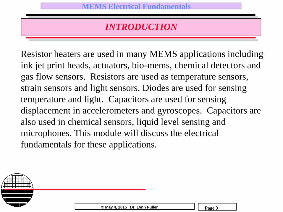
INTRODUCTION
Resistor heaters are used in many MEMS applications including
ink jet print heads, actuators, bio-mems, chemical detectors and
gas flow sensors. Resistors are used as temperature sensors,
strain sensors and light sensors. Diodes are used for sensing
temperature and light. Capacitors are used for sensing
displacement in accelerometers and gyroscopes. Capacitors are
also used in chemical sensors, liquid level sensing and
microphones. This module will discuss the electrical
fundamentals for these applications.

© May 4, 2015 Dr. Lynn Fuller
MEMS Electrical Fundamentals
Page 4
OHM’S LAW
I
V
Resistor a two terminal device that exhibits a
linear I-V characteristic that goes through the
origin. The inverse slope is the value of the
resistance.
R = V/I = 1/slope
I
V
-
+
R
© May 4, 2015 Dr. Lynn Fuller
MEMS Electrical Fundamentals
Page 5
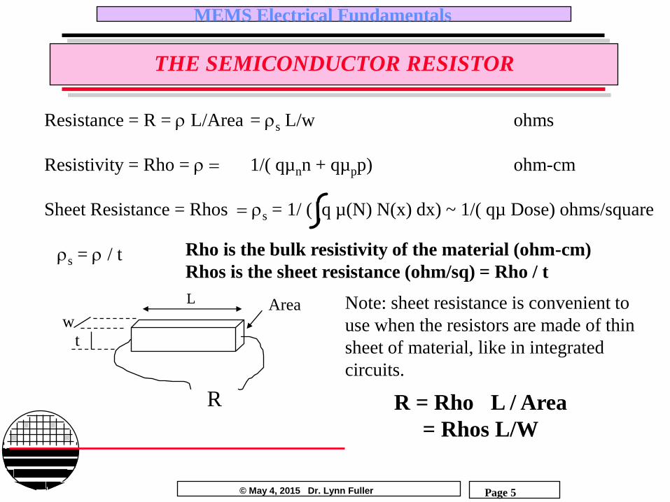
THE SEMICONDUCTOR RESISTOR
Resistance = R = L/Area = s L/w ohms
Resistivity = Rho = 1/( qµnn + qµpp) ohm-cm
Sheet Resistance = Rhos s = 1/ ( q µ(N) N(x) dx) ~ 1/( qµ Dose) ohms/square
L Area
R
w t
s = / t
Note: sheet resistance is convenient to
use when the resistors are made of thin
sheet of material, like in integrated
circuits.
R = Rho L / Area
= Rhos L/W
Rho is the bulk resistivity of the material (ohm-cm)
Rhos is the sheet resistance (ohm/sq) = Rho / t
© May 4, 2015 Dr. Lynn Fuller
MEMS Electrical Fundamentals
Page 6
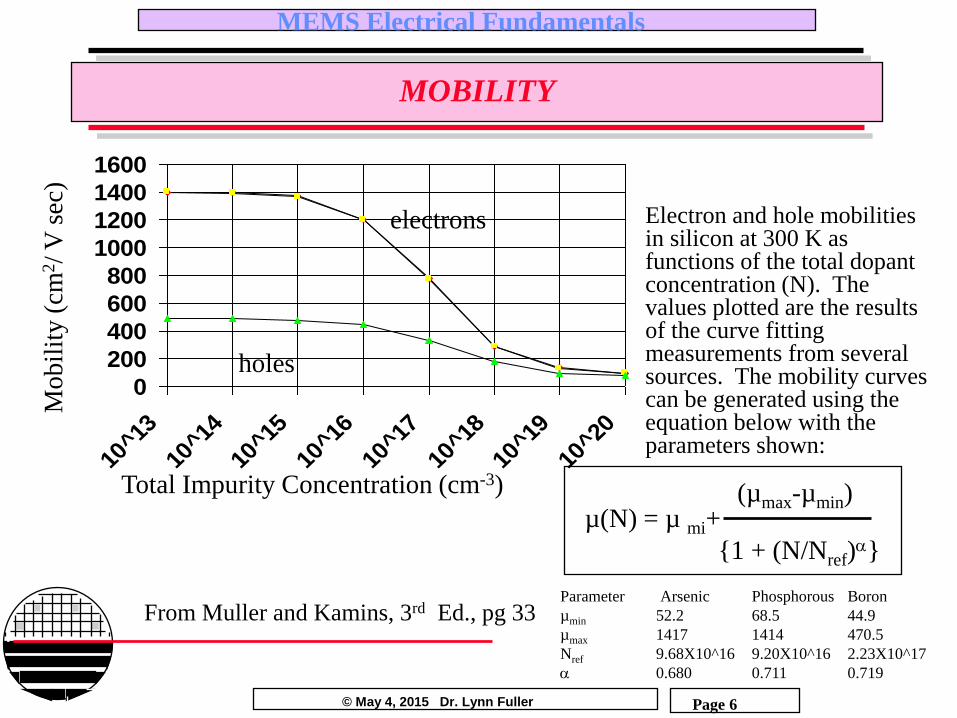
MOBILITY
Total Impurity Concentration (cm-3)
0
200
400
600
800
1000
1200
1400
1600
10^13
10^14
10^15
10^16
10^17
10^18
10^19
10^20
ArsenicBoronPhosphorus
Mo
bil
ity (
cm2/
V s
ec)
electrons
holes
Parameter Arsenic Phosphorous Boron
µmin 52.2 68.5 44.9
µmax 1417 1414 470.5
Nref 9.68X10^16 9.20X10^16 2.23X10^17
0.680 0.711 0.719
µ(N) = µ mi+ (µmax-µmin)
{1 + (N/Nref)}
Electron and hole mobilities in silicon at 300 K as functions of the total dopant concentration (N). The values plotted are the results of the curve fitting measurements from several sources. The mobility curves can be generated using the equation below with the parameters shown:
From Muller and Kamins, 3rd Ed., pg 33
© May 4, 2015 Dr. Lynn Fuller
MEMS Electrical Fundamentals
Page 7
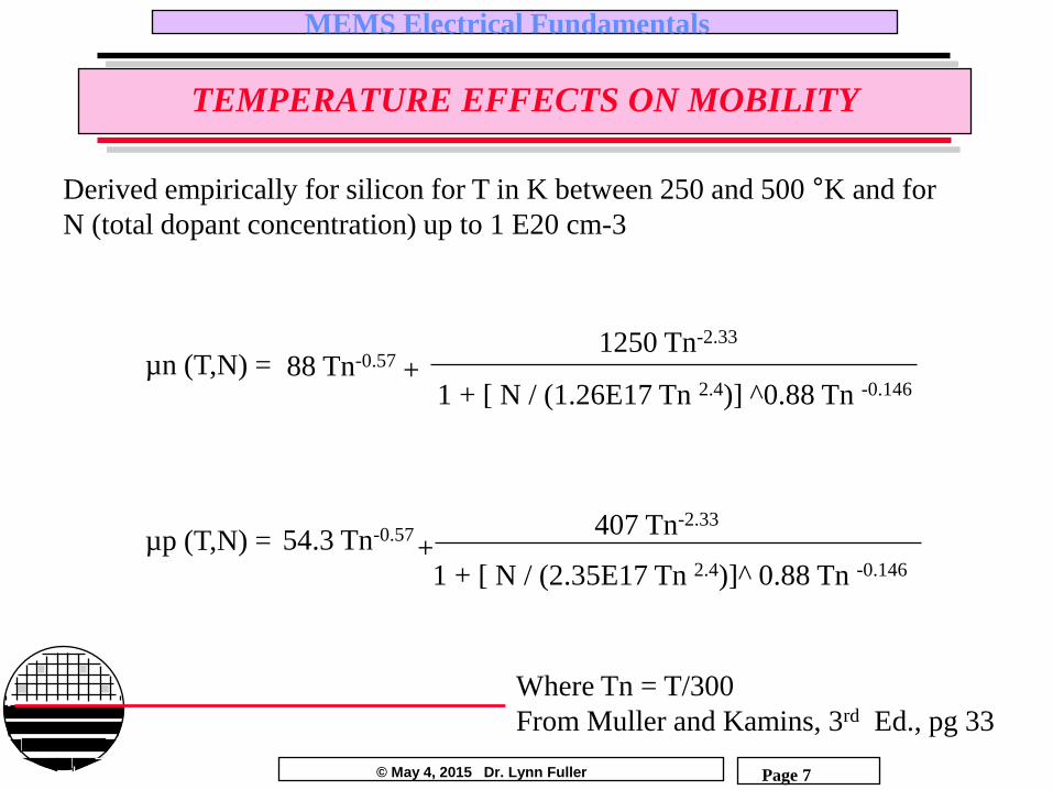
TEMPERATURE EFFECTS ON MOBILITY
Derived empirically for silicon for T in K between 250 and 500 °K and for
N (total dopant concentration) up to 1 E20 cm-3
µn (T,N) =
µp (T,N) =
88 Tn-0.57
54.3 Tn-0.57
Where Tn = T/300
From Muller and Kamins, 3rd Ed., pg 33
1250 Tn-2.33
407 Tn-2.33
1 + [ N / (1.26E17 Tn 2.4)] ^0.88 Tn -0.146
1 + [ N / (2.35E17 Tn 2.4)]^ 0.88 Tn -0.146
+
+

© May 4, 2015 Dr. Lynn Fuller
MEMS Electrical Fundamentals
Page 8
MOBILITY CALCULATIONS
This spreadsheet calculates the mobility from the equations given
by Kamins, Muller and Chan, shown on the previous two pages.

© May 4, 2015 Dr. Lynn Fuller
MEMS Electrical Fundamentals
Page 9
TEMPERATURE COEFFICIENT OF RESISTANCE
R/T for semiconductor resistors R = Rhos L/W = Rho/t L/W assume W, L, t do not change with T Rho = 1/(qµn + qµp) where µ is the mobility which is a function of temperature, n and p are the carrier concentrations which can be a function of temperature (in lightly doped semiconductors) as T increases, µ decreases, n or p may increase and the result is that R usually increases unless the decrease in µ is cancelled by the increase in n or p
© May 4, 2015 Dr. Lynn Fuller
MEMS Electrical Fundamentals
Page 10
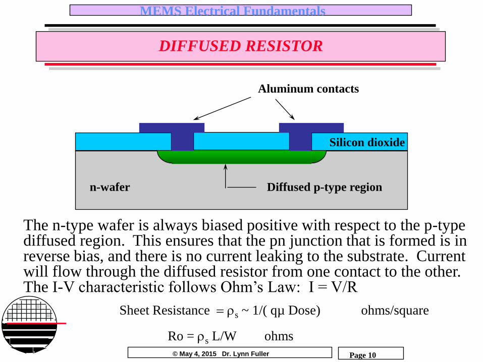
DIFFUSED RESISTOR
Aluminum contacts
The n-type wafer is always biased positive with respect to the p-type diffused region. This ensures that the pn junction that is formed is in reverse bias, and there is no current leaking to the substrate. Current will flow through the diffused resistor from one contact to the other. The I-V characteristic follows Ohm’s Law: I = V/R
n-wafer Diffused p-type region
Silicon dioxide
Sheet Resistance s ~ 1/( qµ Dose) ohms/square Ro = s L/W ohms

© May 4, 2015 Dr. Lynn Fuller
MEMS Electrical Fundamentals
Page 11
RESISTOR NETWORK
500 W 400 250 W
Desired resistor network
Layout if Rhos = 100 ohms/square
L
W

© May 4, 2015 Dr. Lynn Fuller
MEMS Electrical Fundamentals
Page 12
R AND C IN AN INTEGRATED CIRCUIT
Estimate the sheet resistance of the 4000 ohm resistor shown.
R
C
741 OpAmp

© May 4, 2015 Dr. Lynn Fuller
MEMS Electrical Fundamentals
Page 13
DIFFUSION FROM A CONSTANT SOURCE
N(x,t) = No erfc (x/2 Dptp)
Solid Solubility Limit, No
x
into wafer
Wafer Background Concentration, NBC
N(x,t)
Xj
p-type
n-type
erfc function
for erfc predeposit
Q’A (tp) = QA(tp)/Area = 2 No (Dptp) / Dose
Where Dp is the diffusion constant at the predeposit temperature and tp is the predeposit time
© May 4, 2015 Dr. Lynn Fuller
MEMS Electrical Fundamentals
Page 14
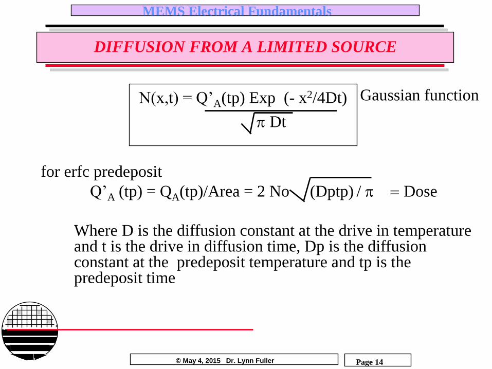
DIFFUSION FROM A LIMITED SOURCE
for erfc predeposit
Q’A (tp) = QA(tp)/Area = 2 No (Dptp) / Dose
N(x,t) = Q’A(tp) Exp (- x2/4Dt)
Dt
Where D is the diffusion constant at the drive in temperature and t is the drive in diffusion time, Dp is the diffusion constant at the predeposit temperature and tp is the predeposit time
Gaussian function
© May 4, 2015 Dr. Lynn Fuller
MEMS Electrical Fundamentals
Page 15
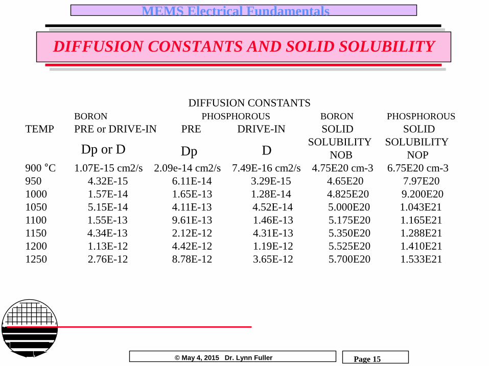
DIFFUSION CONSTANTS AND SOLID SOLUBILITY
DIFFUSION CONSTANTS
BORON PHOSPHOROUS BORON PHOSPHOROUS
TEMP PRE or DRIVE-IN PRE DRIVE-IN SOLID SOLID
SOLUBILITY SOLUBILITY
NOB NOP
900 °C 1.07E-15 cm2/s 2.09e-14 cm2/s 7.49E-16 cm2/s 4.75E20 cm-3 6.75E20 cm-3
950 4.32E-15 6.11E-14 3.29E-15 4.65E20 7.97E20
1000 1.57E-14 1.65E-13 1.28E-14 4.825E20 9.200E20
1050 5.15E-14 4.11E-13 4.52E-14 5.000E20 1.043E21
1100 1.55E-13 9.61E-13 1.46E-13 5.175E20 1.165E21
1150 4.34E-13 2.12E-12 4.31E-13 5.350E20 1.288E21
1200 1.13E-12 4.42E-12 1.19E-12 5.525E20 1.410E21
1250 2.76E-12 8.78E-12 3.65E-12 5.700E20 1.533E21
Dp Dp or D D

© May 4, 2015 Dr. Lynn Fuller
MEMS Electrical Fundamentals
Page 16
ION IMPLANTED RESISTOR
Like the diffused resistor but more accurate control over the sheet resistance. The dose is a machine parameter that is set by the user. Sheet Resistance s ~ 1/( qµ Dose) ohms/square Also the dose can be lower than in a diffused resistor resulting in higher sheet resistance than possible with the diffused resistor.
Aluminum contacts
n-wafer Ion Implanted p-type region
Silicon dioxide
© May 4, 2015 Dr. Lynn Fuller
MEMS Electrical Fundamentals
Page 17
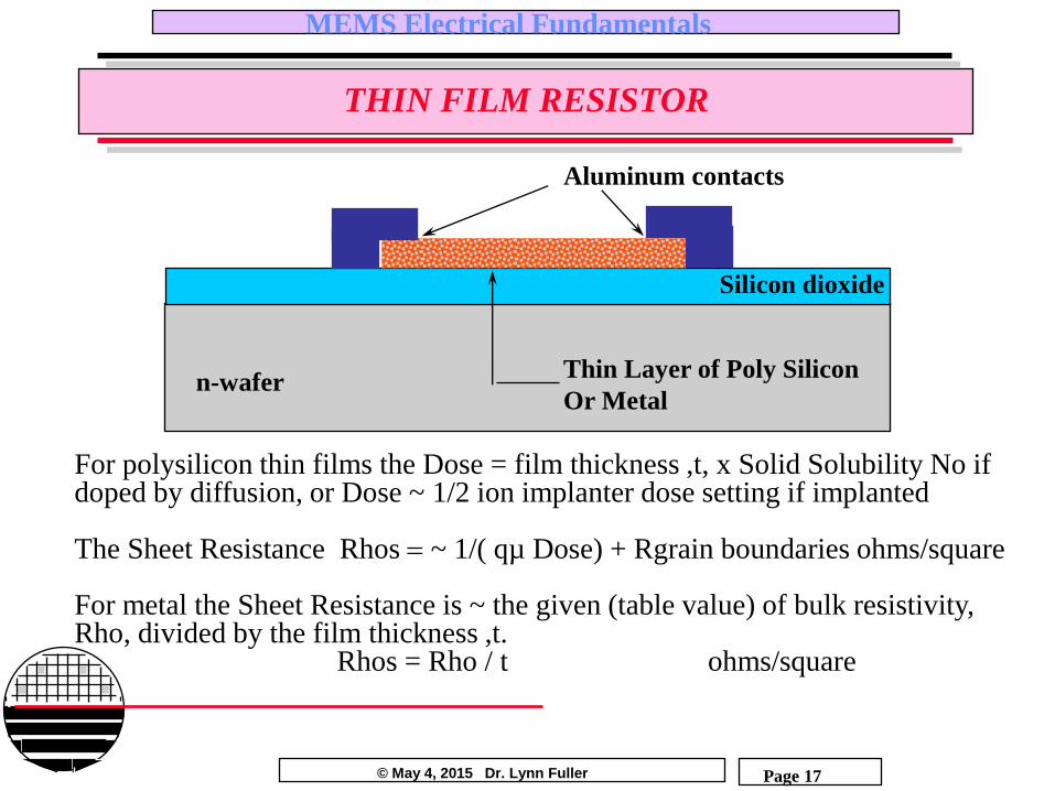
THIN FILM RESISTOR
Aluminum contacts
n-wafer Thin Layer of Poly Silicon
Or Metal
Silicon dioxide
For polysilicon thin films the Dose = film thickness ,t, x Solid Solubility No if doped by diffusion, or Dose ~ 1/2 ion implanter dose setting if implanted The Sheet Resistance Rhos ~ 1/( qµ Dose) + Rgrain boundaries ohms/square For metal the Sheet Resistance is ~ the given (table value) of bulk resistivity, Rho, divided by the film thickness ,t. Rhos = Rho / t ohms/square

© May 4, 2015 Dr. Lynn Fuller
MEMS Electrical Fundamentals
Page 18
POLY SILICON
Grain boundary take up some of the implanted dose. They also add resistance to the resistor that is less sensitive to temperature and doping concentration. We assume grain size ~ equal to ½ the film thickness (t) and the number of grains equals the path length (L) divided by grain size (t/2). Each grain boundary adds a fixed resistance which is found empirically. (example 0.9 ohms)
© May 4, 2015 Dr. Lynn Fuller
MEMS Electrical Fundamentals
Page 19
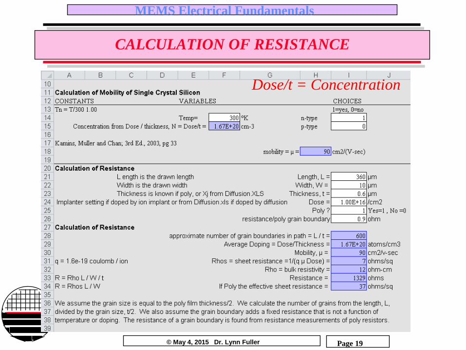
CALCULATION OF RESISTANCE
Dose/t = Concentration

© May 4, 2015 Dr. Lynn Fuller
MEMS Electrical Fundamentals
Page 20
POLY RESISTOR
Poly
R = 1/SLOPE
= 1/0.681m
= 1468 ohm
Rhos = 1468/39
=37.6 ohm/sq
Use t=0.6, L=390u, W=10u Dose =1e16cm-2, N-type poly, and 0.9 ohms per boundary

© May 4, 2015 Dr. Lynn Fuller
MEMS Electrical Fundamentals
Page 21
RESISTOR I-V CHARACTERISTICS
R= 1/1.44e-3
= 694 ohms
Use t=1.5u, L=500u, W=100u Dose =0.5e15cm-2 p-type single crystal silicon
Gives R=683 ohms

© May 4, 2015 Dr. Lynn Fuller
MEMS Electrical Fundamentals
Page 22
CLOSE UP OF RESISTORS AND THERMOCOUPLE
Red N+ Polysilicon Resistor 60 um x 20 um + 30 to contact so L/W ~ 6
Green P+ Diffused Resistor 200 um wide x 180 um long
Aluminum – N+ Poly Thermocouple
Use t=0.5, L=120, w=20 dose =1e16, n-type poly, and 0.9 ohms per boundary Rmeas = 448
Use t=1.5, L=180, w=200 dose =2e14, p-type crystalline, Rmeas = 207
© May 4, 2015 Dr. Lynn Fuller
MEMS Electrical Fundamentals
Page 23
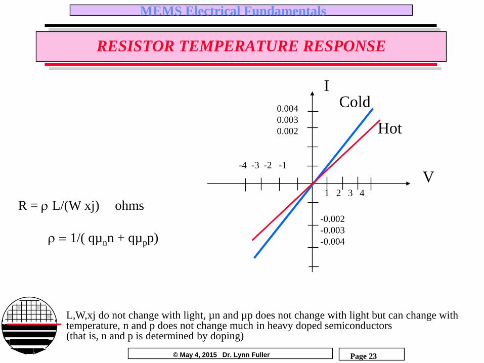
RESISTOR TEMPERATURE RESPONSE
I
V 1 2 3 4
-4 -3 -2 -1
-0.002
-0.003
-0.004
0.004
0.003
0.002
Cold
Hot
L,W,xj do not change with light, µn and µp does not change with light but can change with temperature, n and p does not change much in heavy doped semiconductors (that is, n and p is determined by doping)
R = L/(W xj) ohms
1/( qµnn + qµpp)

© May 4, 2015 Dr. Lynn Fuller
MEMS Electrical Fundamentals
Page 24
RESISTOR LIGHT RESPONSE
No light
Full light
R = L/(W xj) ohms
1/( qµnn + qµpp)
L,W,xj do not change with light, µn and µp does not change with light but can change with temperature, n and p does not change much in heavy doped semiconductors (that is, n and p is determined by doping)

© May 4, 2015 Dr. Lynn Fuller
MEMS Electrical Fundamentals
Page 25
HEATERS
P= IV = I2R watts
Final steady state temperature
depends on power density in
watts/cm2
and
the thermal resistance
from heater to ambient
I
V
-
+
R = s L/W

© May 4, 2015 Dr. Lynn Fuller
MEMS Electrical Fundamentals
Page 26
THERMAL CONDUCTIVITY
Temp ambient
Thermal Resistance, Rth
to ambient
Temp above ambient
Power input
Rth = 1/C L/Area where C=thermal conductivity L= thickness of layer between heater and ambient Area = cross sectional area of the path to ambient

© May 4, 2015 Dr. Lynn Fuller
MEMS Electrical Fundamentals
Page 27
THERMAL PROPERTIES OF SOME MATERIALS
MP Coefficient Thermal Specific °C of Thermal Conductivity Heat Expansion ppm/°C w/cmK cal/gm°C Diamond 1.0 20 Single Crystal Silicon 1412 2.33 1.5 Poly Silicon 1412 2.33 1.5 Silicon Dioxide 1700 0.55 0.014 Silicon Nitride 1900 0.8 0.185 Aluminum 660 22 2.36 0.215 Nickel 1453 13.5 0.90 0.107 Chrome 1890 5.1 0.90 0.03 Copper 1357 16.1 3.98 0.092 Gold 1062 14.2 0.032 Tungsten 3370 4.5 1.78 Titanium 1660 8.9 0.17 Tantalum 2996 6.5 0.54 Air 0.00026 0.24 Water 0 0.0061 1.00
1 watt = 0.239 cal/sec

© May 4, 2015 Dr. Lynn Fuller
MEMS Electrical Fundamentals
Page 28
HEATER EXAMPLE
Example: Poly heater 100x100µm has sheet resistance of 25 ohms/sq and 9 volts is applied. What temperature will it reach if built on 1 µm thick oxide?
Power = V2/R = 81/25 = 3.24 watt
Rthermal = 1/C L/Area = (1/0.014 watt/cm °C)(1e-4cm/(100e-4cm x100e-4cm))
= 71.4 °C/watt
Temperature = Tambient + (3.24) (71.4) = Tambient + 231 °C
© May 4, 2015 Dr. Lynn Fuller
MEMS Electrical Fundamentals
Page 29
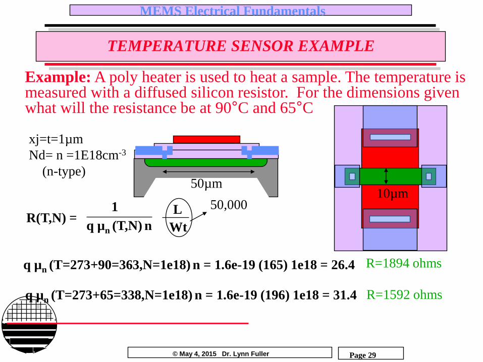
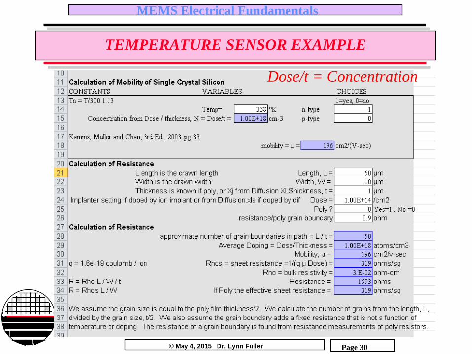
TEMPERATURE SENSOR EXAMPLE
Example: A poly heater is used to heat a sample. The temperature is measured with a diffused silicon resistor. For the dimensions given what will the resistance be at 90°C and 65°C
R(T,N) = 1
q µn (T,N) n
L
Wt
50µm 10µm
xj=t=1µm
Nd= n =1E18cm-3
(n-type)
q µn (T=273+65=338,N=1e18) n = 1.6e-19 (196) 1e18 = 31.4
q µn (T=273+90=363,N=1e18) n = 1.6e-19 (165) 1e18 = 26.4
50,000
R=1894 ohms
R=1592 ohms
© May 4, 2015 Dr. Lynn Fuller
MEMS Electrical Fundamentals
Page 30
TEMPERATURE SENSOR EXAMPLE
Dose/t = Concentration

© May 4, 2015 Dr. Lynn Fuller
MEMS Electrical Fundamentals
Page 31
DIODES AND HEATERS
Poly Heater on top of Diodes
Integrated n-well series resistor.
VDD
Vo ~ 0.6
-2.2mV/°C
I
V
T1 T2
T2>T1
I ~ (VDD-0.6)/R
R

© May 4, 2015 Dr. Lynn Fuller
MEMS Electrical Fundamentals
Page 32
UNIFORMLY DOPED PN JUNCTION
n-type
p-type
Space Charge Layer
Potential,
Electric Field,
charge density,
n = ND p = NA
+qND
-W1
W2
+VR
x
+VR
-qNA
Ionized Immobile Phosphrous donor atom
Ionized Immobile Boron acceptor atom
Phosphrous donor atom and electron P+ -
B- +
Boron acceptor atom and hole
qNA W1 =qND W2
P+
B- B- +
B- +
P+ -
P+ B-
B- B-
P+
P+ P+ P+ -
P+ -
P+ -
P+ -
© May 4, 2015 Dr. Lynn Fuller
MEMS Electrical Fundamentals
Page 33
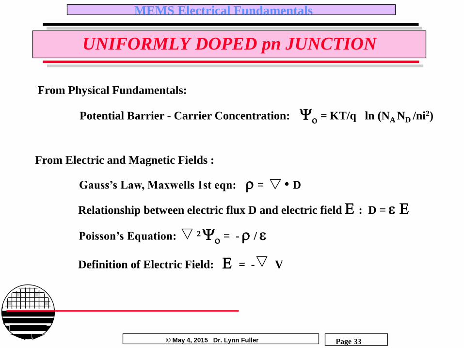
UNIFORMLY DOPED pn JUNCTION
From Physical Fundamentals:
Relationship between electric flux D and electric field : D =
Gauss’s Law, Maxwells 1st eqn: = D
Poisson’s Equation: 2 = - /
Definition of Electric Field: = - V
Potential Barrier - Carrier Concentration: = KT/q ln (NA ND /ni2)
From Electric and Magnetic Fields :

© May 4, 2015 Dr. Lynn Fuller
MEMS Electrical Fundamentals
Page 34
EXAMPLE CALCULATIONS
Width of space
charge layer depends
on the doping on
both sides and the
applied reverse bias
voltage and
temperature.

© May 4, 2015 Dr. Lynn Fuller
MEMS Electrical Fundamentals
Page 35
CURRENTS IN PN JUNCTIONS
Vbi = turn on voltage
~ 0.7 volts for Si
VD
Id
VRB = reverse
breakdown voltage
p n
Id
+ VD -
Forward Bias
Reverse Bias
Id = Is [EXP (q VD/KT) -1]
Is
Ideal diode equation

© May 4, 2015 Dr. Lynn Fuller
MEMS Electrical Fundamentals
Page 36
INTEGRATED DIODES
p-wafer
n+ p+ n-well
p+ means heavily doped p-type n+ means heavily doped n-type n-well is an n-region at slightly higher doping than the p-wafer
Note: there are actually two pn junctions, the well-wafer pn
junction should always be reverse biased
© May 4, 2015 Dr. Lynn Fuller
MEMS Electrical Fundamentals
Page 37
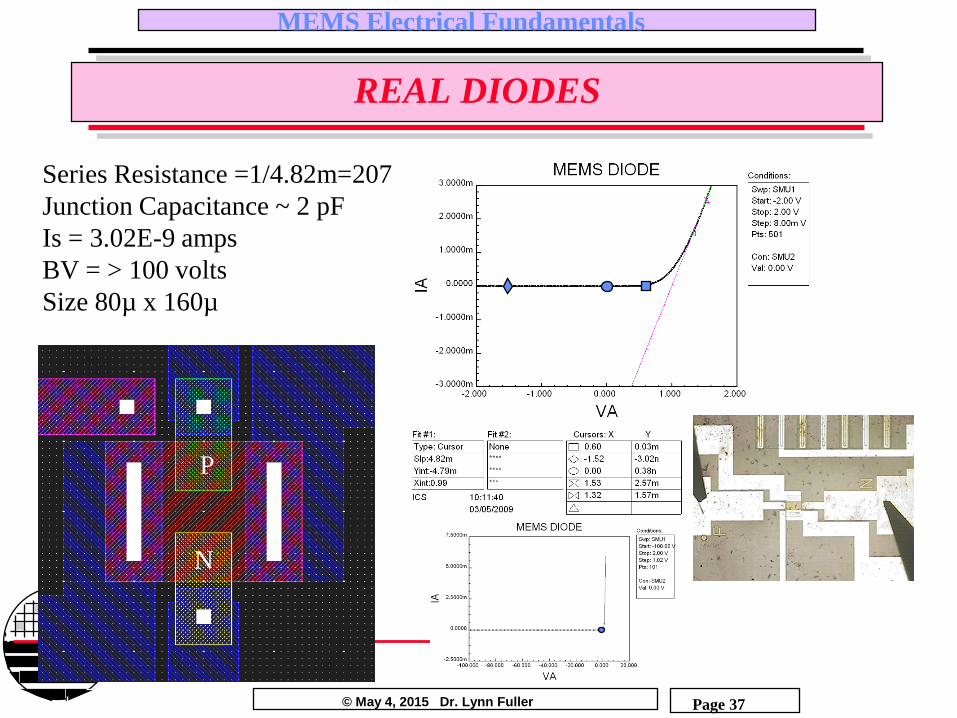
REAL DIODES
Series Resistance =1/4.82m=207
Junction Capacitance ~ 2 pF
Is = 3.02E-9 amps
BV = > 100 volts
Size 80µ x 160µ
N
P

© May 4, 2015 Dr. Lynn Fuller
MEMS Electrical Fundamentals
Page 38
DIODE SPICE MODEL
MEMS Diode
Model Parameter Default Value Extracted Value
Is reverse saturation current 1e-14 A 3.02E-9 A
N emission coefficient 1 1
RS series resistance 0 207 ohms
VJ built-in voltage 1 V 0.6
CJ0 zero bias junction capacitance 0 2pF
M grading coefficient 0.5 0.5
BV Breakdown voltage infinite 400
IBV Reverse current at breakdown 1E-10 A -
DXXX N(anode) N(cathode) Modelname
.model Modelname D Is=1e-14 Cjo=.1pF Rs=.1
.model RITMEMS D IS=3.02E-9 N=1 RS=207
+VJ=0.6 CJ0=2e-12 M-0.5 BV=400
DIODE Parameters
© May 4, 2015 Dr. Lynn Fuller
MEMS Electrical Fundamentals
Page 39
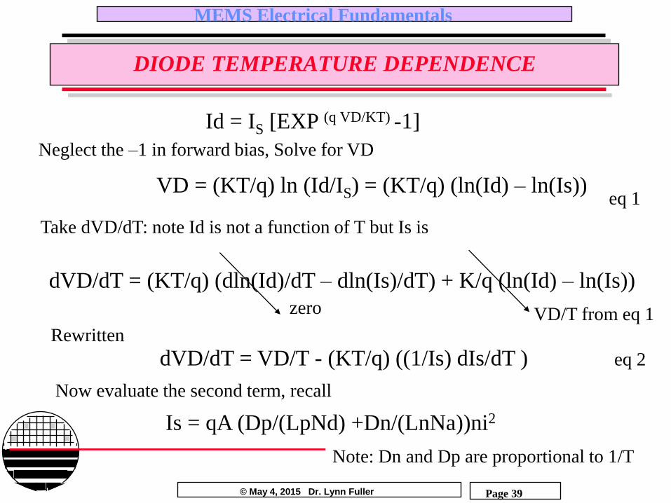
DIODE TEMPERATURE DEPENDENCE
Id = IS [EXP (q VD/KT) -1]
Neglect the –1 in forward bias, Solve for VD
VD = (KT/q) ln (Id/IS) = (KT/q) (ln(Id) – ln(Is))
Take dVD/dT: note Id is not a function of T but Is is
dVD/dT = (KT/q) (dln(Id)/dT – dln(Is)/dT) + K/q (ln(Id) – ln(Is))
zero VD/T from eq 1 Rewritten
dVD/dT = VD/T - (KT/q) ((1/Is) dIs/dT )
Now evaluate the second term, recall
Is = qA (Dp/(LpNd) +Dn/(LnNa))ni2
eq 1
eq 2
Note: Dn and Dp are proportional to 1/T
© May 4, 2015 Dr. Lynn Fuller
MEMS Electrical Fundamentals
Page 40
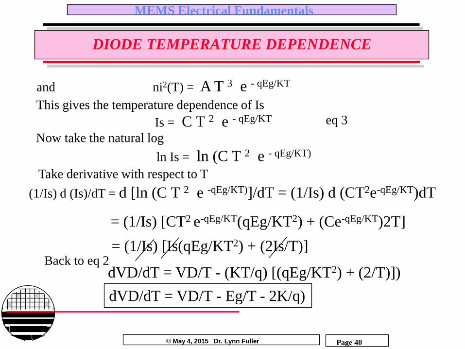
DIODE TEMPERATURE DEPENDENCE
and ni2(T) = A T 3 e - qEg/KT
This gives the temperature dependence of Is
Is = C T 2 e - qEg/KT
Now take the natural log
ln Is = ln (C T 2 e - qEg/KT)
Take derivative with respect to T
(1/Is) d (Is)/dT = d [ln (C T 2 e -qEg/KT)]/dT = (1/Is) d (CT2e-qEg/KT)dT
eq 3
= (1/Is) [CT2 e-qEg/KT(qEg/KT2) + (Ce-qEg/KT)2T]
= (1/Is) [Is(qEg/KT2) + (2Is/T)] Back to eq 2
dVD/dT = VD/T - (KT/q) [(qEg/KT2) + (2/T)])
dVD/dT = VD/T - Eg/T - 2K/q)

© May 4, 2015 Dr. Lynn Fuller
MEMS Electrical Fundamentals
Page 41
EXAMPLE: DIODE TEMPERATURE DEPENDENCE
dVD/dT = VD/T - Eg/T - 2K/q
Silicon with Eg ~ 1.2 eV, VD = 0.6 volts, T=300 °K
dVD/dT = .6/300 – 1.2/300) - (2(1.38E-23)/1.6E-19
= -2.2 mV/°
I
V
T1 T2
T1<T2
© May 4, 2015 Dr. Lynn Fuller
MEMS Electrical Fundamentals
Page 42
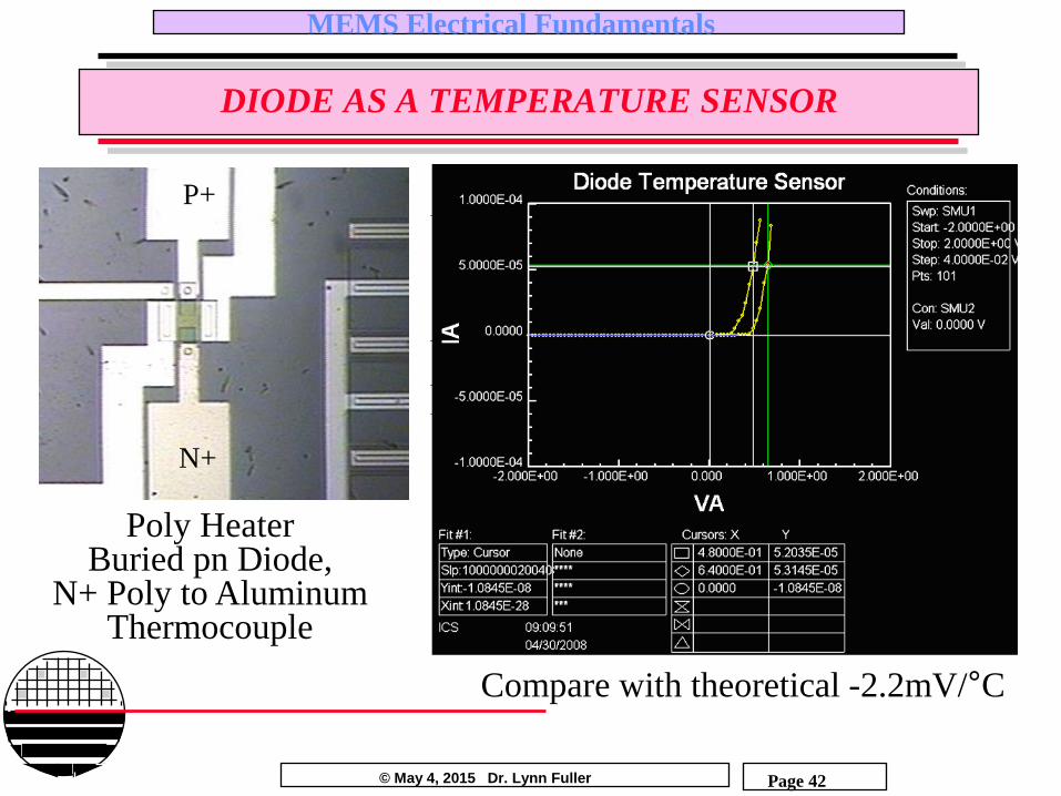
DIODE AS A TEMPERATURE SENSOR
Compare with theoretical -2.2mV/°C
Poly Heater Buried pn Diode,
N+ Poly to Aluminum Thermocouple
P+
N+

© May 4, 2015 Dr. Lynn Fuller
MEMS Electrical Fundamentals
Page 43
SPICE FOR DIODE TEMPERATURE SENSOR

© May 4, 2015 Dr. Lynn Fuller
MEMS Electrical Fundamentals
Page 44
PHOTODIODE
B -
P+ Ionized Immobile Phosphrous donor atom
Ionized Immobile Boron acceptor atom
Phosphrous donor atom and electron P+
-
B-
+ Boron acceptor atom and hole
n-type
p-type
B - P+
B - B -
B - B -
P+ P+ P+ P+
P+
P+
P+
-
B-
+
B - B -
P+
- P+
- P+
-
B-
+
- +
- +
I
electron
and hole
pair
- +
- +
space charge layer

© May 4, 2015 Dr. Lynn Fuller
MEMS Electrical Fundamentals
Page 45
CHARGE GENERATION IN SEMICONDUCTORS
E = h = hc /
What wavelengths will not
generate e-h pairs in silicon.
Thus silicon is transparent or
light of this wavelength or
longer is not adsorbed?
From: Micromachined Transducers,
Gregory T.A. Kovacs
Material Bandgap
eV @ 300°K
max
(um)
GaN 3.360 0.369
ZnO 3.350 0.370
SiC 2.996 0.414
CdS 2.420 0.512
GaP 2.260 0.549
CdSe 1.700 0.729
GaAs 1.420 0.873
InP 1.350 0.919
Si 1.120 1.107
Ge 0.660 1.879
PbS 0.410 3.024
PbTe 0.310 4.000
InSb 0.170 7.294

© May 4, 2015 Dr. Lynn Fuller
MEMS Electrical Fundamentals
Page 46
CHARGE GENERATION vs WAVELENGTH
I I
n-type
p-type
1 3 4 2
E = h = hc /
h = 6.625 e-34 j/s
= (6.625 e-34/1.6e-19) eV/s
E = 1.55 eV (red)
E = 2.50 eV (green)
E = 4.14 eV (blue) B - P+
B - B -
B - B -
P+ P+ P+ P+
P+
P+
P+
-
B-
+
B - B -
P+
- P+
- P+
-
B-
+
- + -
+ -
+
© May 4, 2015 Dr. Lynn Fuller
MEMS Electrical Fundamentals
Page 47
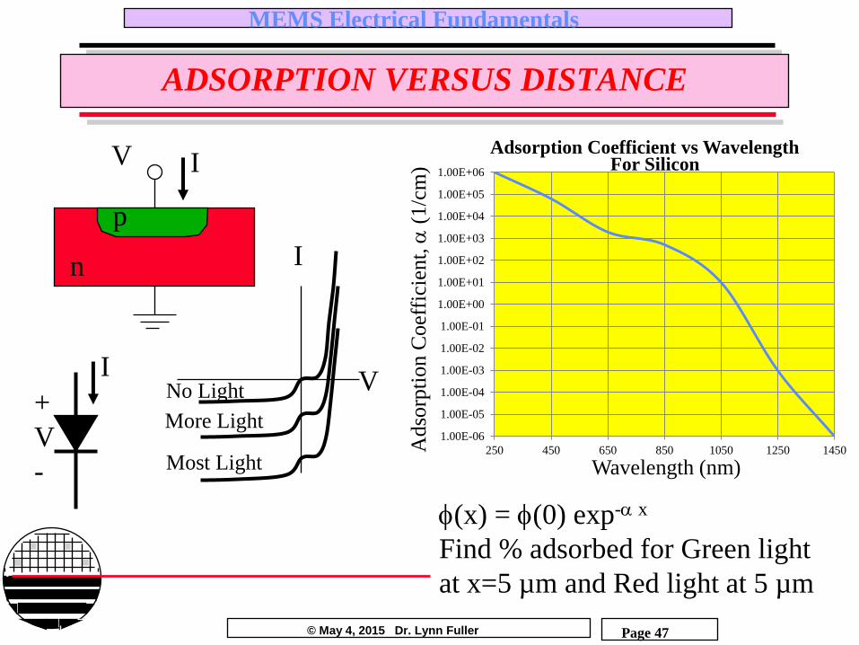
ADSORPTION VERSUS DISTANCE
I
V
n
p
I V
I
+
V
-
More Light
No Light
Most Light
f(x) = f(0) exp- x
Find % adsorbed for Green light
at x=5 µm and Red light at 5 µm
1.00E-06
1.00E-05
1.00E-04
1.00E-03
1.00E-02
1.00E-01
1.00E+00
1.00E+01
1.00E+02
1.00E+03
1.00E+04
1.00E+05
1.00E+06
250 450 650 850 1050 1250 1450
Adsorption Coefficient vs Wavelength
Wavelength (nm)
Adso
rpti
on C
oef
fici
ent,
(
1/c
m) For Silicon
© May 4, 2015 Dr. Lynn Fuller
MEMS Electrical Fundamentals
Page 48
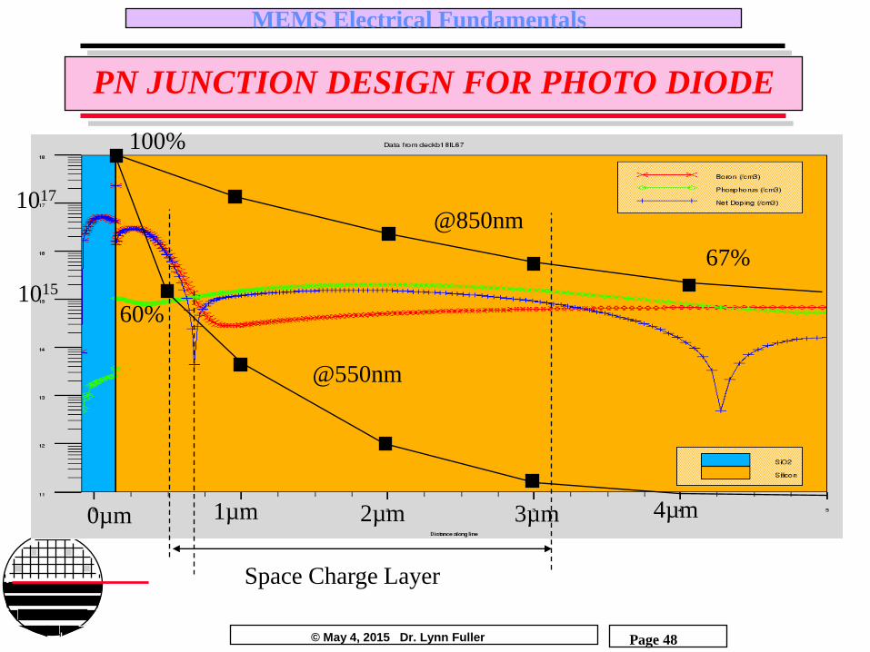
PN JUNCTION DESIGN FOR PHOTO DIODE
0µm 1µm 2µm 3µm 4µm
67%
100%
@850nm
@550nm
1017
1015
Space Charge Layer
60%
© May 4, 2015 Dr. Lynn Fuller
MEMS Electrical Fundamentals
Page 49
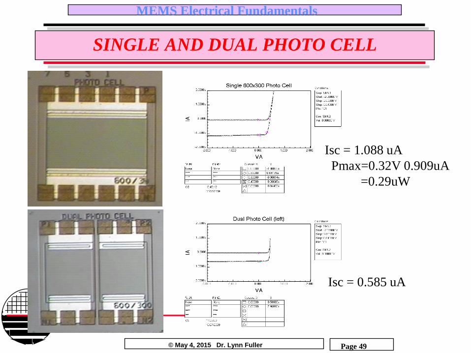
SINGLE AND DUAL PHOTO CELL
Isc = 0.585 uA
Isc = 1.088 uA
Pmax=0.32V 0.909uA
=0.29uW

© May 4, 2015 Dr. Lynn Fuller
MEMS Electrical Fundamentals
Page 50
CAPACITORS
Capacitor - a two terminal device whose current is proportional to the time rate of change of the applied voltage; I = C dV/dt a capacitor C is constructed of any two conductors separated by an insulator. The capacitance of such a structure is: C = o r Area/d where o is the permitivitty of free space r is the relative permitivitty Area is the overlap area of the two conductor separated by distance d
o = 8.85E-14 F/cm
I
C V
+
-
Area
d r air = 1 r SiO2 = 3.9
© May 4, 2015 Dr. Lynn Fuller
MEMS Electrical Fundamentals
Page 51
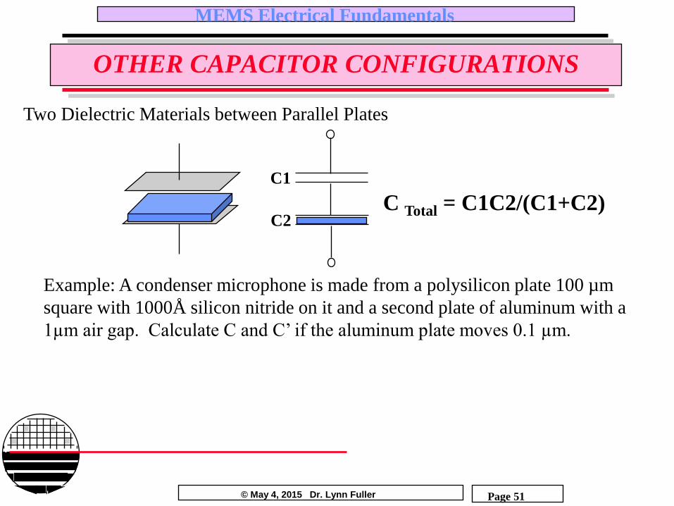
OTHER CAPACITOR CONFIGURATIONS
C2
C1
C Total = C1C2/(C1+C2)
Two Dielectric Materials between Parallel Plates
Example: A condenser microphone is made from a polysilicon plate 100 µm
square with 1000Å silicon nitride on it and a second plate of aluminum with a
1µm air gap. Calculate C and C’ if the aluminum plate moves 0.1 µm.
© May 4, 2015 Dr. Lynn Fuller
MEMS Electrical Fundamentals
Page 52
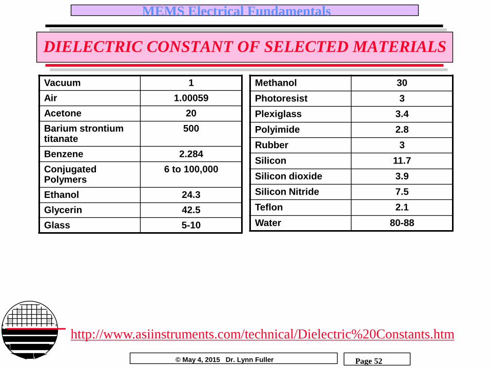
DIELECTRIC CONSTANT OF SELECTED MATERIALS
Vacuum 1
Air 1.00059
Acetone 20
Barium strontium titanate
500
Benzene 2.284
Conjugated Polymers
6 to 100,000
Ethanol 24.3
Glycerin 42.5
Glass 5-10
Methanol 30
Photoresist 3
Plexiglass 3.4
Polyimide 2.8
Rubber 3
Silicon 11.7
Silicon dioxide 3.9
Silicon Nitride 7.5
Teflon 2.1
Water 80-88
http://www.asiinstruments.com/technical/Dielectric%20Constants.htm

© May 4, 2015 Dr. Lynn Fuller
MEMS Electrical Fundamentals
Page 53
CALCULATIONS

© May 4, 2015 Dr. Lynn Fuller
MEMS Electrical Fundamentals
Page 54
OTHER CAPACITOR CONFIGURATIONS
Interdigitated Fingers with Thickness > Space between Fingers
h = height of fingers s = space between fingers N = number of fingers L = length of finger overlap
C = (N-1) or L h /s
Example:

© May 4, 2015 Dr. Lynn Fuller
MEMS Electrical Fundamentals
Page 55
OTHER CAPACITOR CONFIGURATIONS
Interdigitated Fingers with Thickness << Space between Fingers
C = LN 4 or
n=1
0 0 1
2n-1 Jo2 (2n-1)s
2(s+w)
Jo = zero order Bessel function w = width of fingers s = space between fingers N = number of fingers L = length of finger overlap
Reference:
Lvovich, Liu and Smiechowski,

© May 4, 2015 Dr. Lynn Fuller
MEMS Electrical Fundamentals
Page 56
OTHER CAPACITOR CONFIGURATIONS
Two Long Parallel Wires Surrounded by Dielectric Material
C/L = 12.1 r / (log [(h/r) + ((h/r)2-1)1/2]
h = half center to center space r = conductor radius (same units as h)
Capacitance per unit length C/L
Reference: Kraus and Carver
Example: Calculate the capacitance of a meter long connection of parallel wires.
Solution: let, h = 1 mm, r = 0.5mm, plastic er = 3 the equation above gives
C/L = 63.5 pF/m
C = 63.5 pF

© May 4, 2015 Dr. Lynn Fuller
MEMS Electrical Fundamentals
Page 57
OTHER CAPACITOR CONFIGURATIONS
Coaxial Cable
C/L = 2 r / ln(b/a)
b = inside radius of outside conductor a = radius of inside conductor
Capacitance per unit length C/L
Reference: Kraus and Carver
Example: Calculate the capacitance of a meter long coaxial cable.
Solution: let b = 5 mm, a = 0.2mm, plastic er = 3 the equation above gives
C/L = 51.8 pF/m
C = 51.8 pF

© May 4, 2015 Dr. Lynn Fuller
MEMS Electrical Fundamentals
Page 58
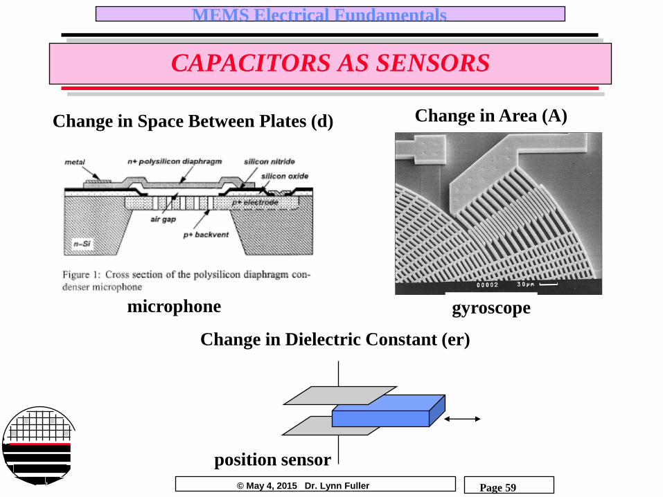
CAPACITORS AS SENSORS
C d
C1
C2
C
d
C1
d
C2
One plate moves relative to other changing gap (d)
One plate moves relative to other
changing overlap area (A)
Center plate moves relative to the two
fixed plates
© May 4, 2015 Dr. Lynn Fuller
MEMS Electrical Fundamentals
Page 59
CAPACITORS AS SENSORS
Change in Space Between Plates (d) Change in Area (A)
Change in Dielectric Constant (er)
microphone gyroscope
position sensor
© May 4, 2015 Dr. Lynn Fuller
MEMS Electrical Fundamentals
Page 60
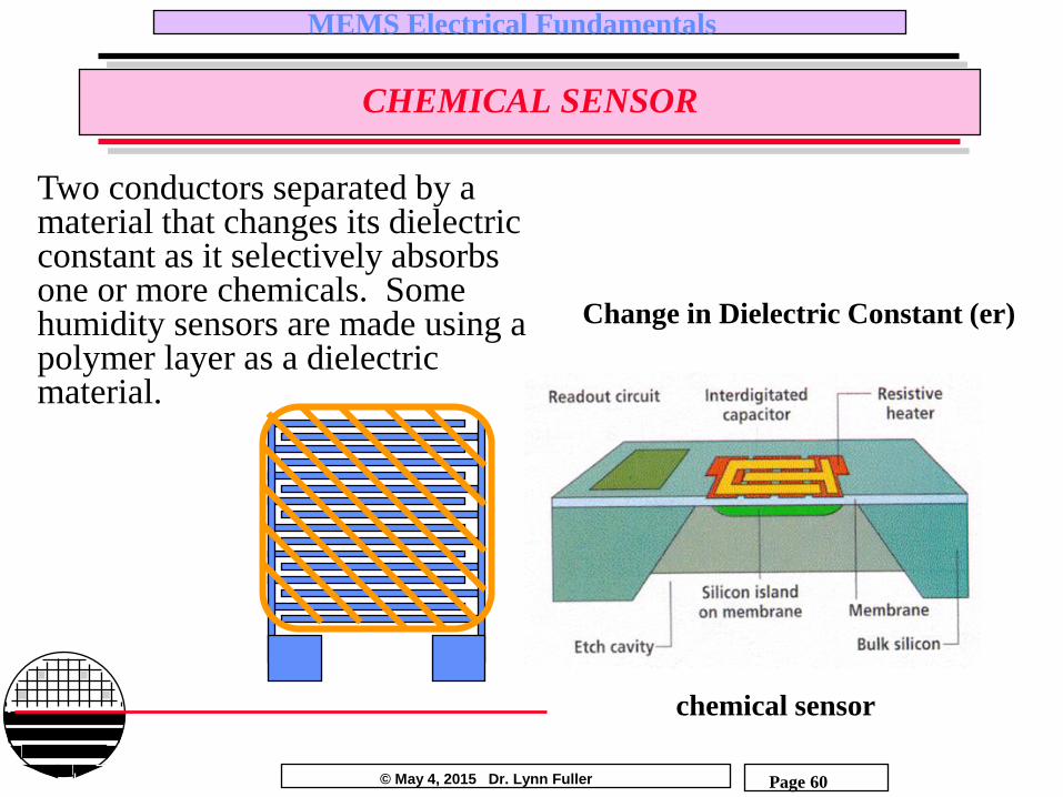
CHEMICAL SENSOR
Two conductors separated by a material that changes its dielectric constant as it selectively absorbs one or more chemicals. Some humidity sensors are made using a polymer layer as a dielectric material.
Change in Dielectric Constant (er)
chemical sensor

© May 4, 2015 Dr. Lynn Fuller
MEMS Electrical Fundamentals
Page 61
REFERENCES
1. Device Electronics for Integrated Circuits, Richard S. Muller, Theodore I. Kamins, John Wiley & Sons., 3rd edition, 2003.
2. Micromachined Transducers, Gregory T.A. Kovacs, McGraw-Hill, 1998.
3. Microsystem Design, Stephen D. Senturia, Kluwer Academic Press, 2001.
4. “Optimization and fabrication of planar interdigitated impedance sensors for highly resistive non-aqueous industrial fluids”, Lvovich, liu and Smiechowski, Sensors and Actuators B:Chemical, Volume 119, Issue 2, 7 Dec. 2006, pgs 490-496.
5. Solar Cells, Martin A. Green, Prentice-Hall
Related Documents