Micron Parallel NOR Flash Embedded Memory Top/Bottom Boot Block 5V Supply M29F200FT/B, M29F400FT/B, M29F800FT/B, M29F160FT/B Features • Supply voltage – V CC = 5V • Access time: 55ns • Program/erase controller – Embedded byte/word program algorithms • Erase suspend and resume modes • Low power consumption – Standby and automatic standby • 100,000 PROGRAM/ERASE cycles per block • Electronic signature – Manufacturer code: 0x01h • Top device codes – M29F200FT: 0x2251 – M29F400FT: 0x2223 – M29F800FT: 0x22D6 – M29F160FT: 0x22D2 • Bottom device codes – M29F200FB: 0x2257 – M29F400FB: 0x22AB – M29F800FB: 0x2258 – M29F160FB: 0x22D8 • RoHS-compliant packages – TSOP48 – SO44 (16Mb not available for this package) • Automotive device grade 3 – Temperature: –40 to +125°C • Automotive device grade 6 – Temperature: –40 to +85°C • Automotive grade certified (AEC-Q100) M29FxxxFT/B Features CCMTD-1725822587-8401 m29fxxxf/t_2mb-16mb.pdf - Rev. C 5/18 EN 1 Micron Technology, Inc. reserves the right to change products or specifications without notice. © 2013 Micron Technology, Inc. All rights reserved. Products and specifications discussed herein are subject to change by Micron without notice.

Welcome message from author
This document is posted to help you gain knowledge. Please leave a comment to let me know what you think about it! Share it to your friends and learn new things together.
Transcript

Micron Parallel NOR Flash EmbeddedMemoryTop/Bottom Boot Block 5V SupplyM29F200FT/B, M29F400FT/B, M29F800FT/B, M29F160FT/B
Features• Supply voltage
– VCC = 5V• Access time: 55ns• Program/erase controller
– Embedded byte/word program algorithms• Erase suspend and resume modes• Low power consumption
– Standby and automatic standby• 100,000 PROGRAM/ERASE cycles per block• Electronic signature
– Manufacturer code: 0x01h• Top device codes
– M29F200FT: 0x2251– M29F400FT: 0x2223– M29F800FT: 0x22D6– M29F160FT: 0x22D2
• Bottom device codes– M29F200FB: 0x2257– M29F400FB: 0x22AB– M29F800FB: 0x2258– M29F160FB: 0x22D8
• RoHS-compliant packages– TSOP48– SO44 (16Mb not available for this package)
• Automotive device grade 3– Temperature: –40 to +125°C
• Automotive device grade 6– Temperature: –40 to +85°C
• Automotive grade certified (AEC-Q100)
M29FxxxFT/BFeatures
CCMTD-1725822587-8401m29fxxxf/t_2mb-16mb.pdf - Rev. C 5/18 EN 1 Micron Technology, Inc. reserves the right to change products or specifications without notice.
© 2013 Micron Technology, Inc. All rights reserved.
Products and specifications discussed herein are subject to change by Micron without notice.
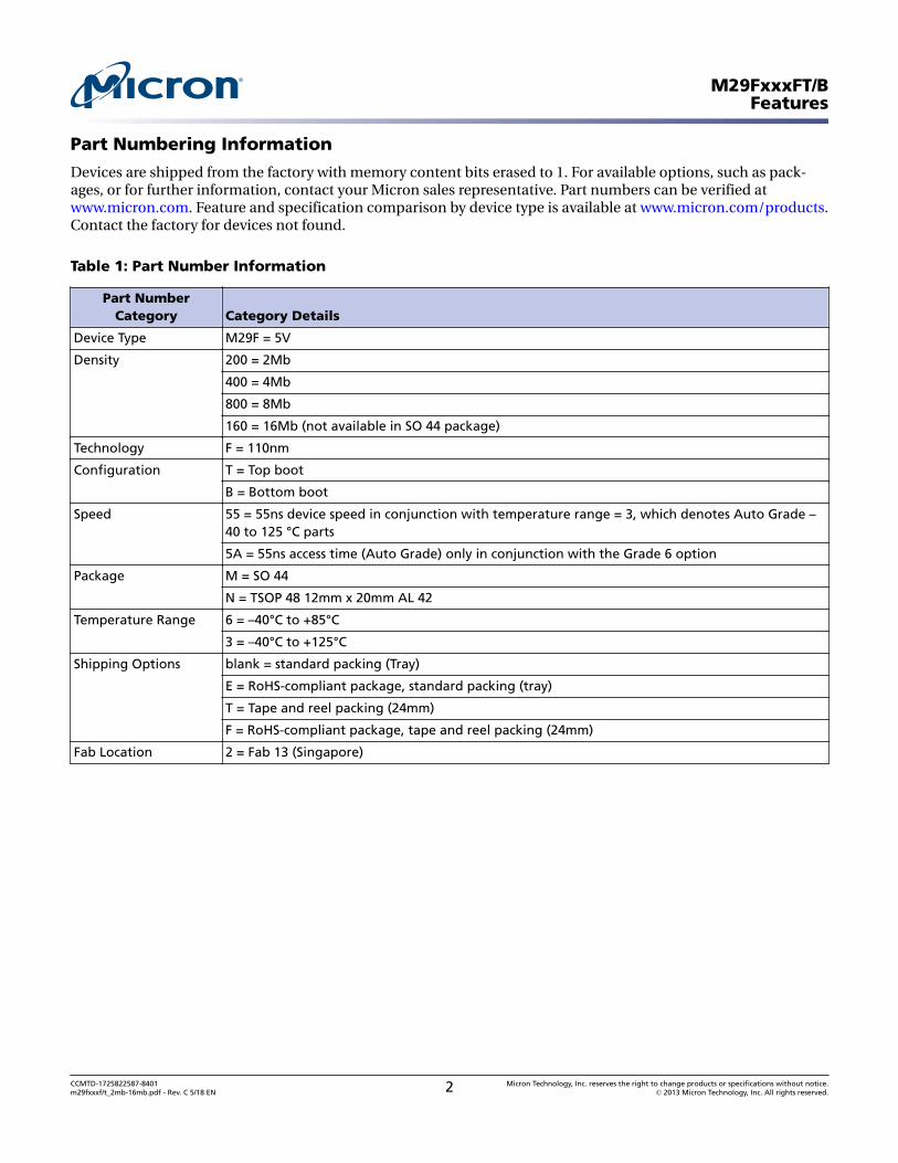
Part Numbering Information
Devices are shipped from the factory with memory content bits erased to 1. For available options, such as pack-ages, or for further information, contact your Micron sales representative. Part numbers can be verified atwww.micron.com. Feature and specification comparison by device type is available at www.micron.com/products.Contact the factory for devices not found.
Table 1: Part Number Information
Part NumberCategory Category Details
Device Type M29F = 5V
Density 200 = 2Mb
400 = 4Mb
800 = 8Mb
160 = 16Mb (not available in SO 44 package)
Technology F = 110nm
Configuration T = Top boot
B = Bottom boot
Speed 55 = 55ns device speed in conjunction with temperature range = 3, which denotes Auto Grade –40 to 125 °C parts
5A = 55ns access time (Auto Grade) only in conjunction with the Grade 6 option
Package M = SO 44
N = TSOP 48 12mm x 20mm AL 42
Temperature Range 6 = –40°C to +85°C
3 = –40°C to +125°C
Shipping Options blank = standard packing (Tray)
E = RoHS-compliant package, standard packing (tray)
T = Tape and reel packing (24mm)
F = RoHS-compliant package, tape and reel packing (24mm)
Fab Location 2 = Fab 13 (Singapore)
M29FxxxFT/BFeatures
CCMTD-1725822587-8401m29fxxxf/t_2mb-16mb.pdf - Rev. C 5/18 EN 2 Micron Technology, Inc. reserves the right to change products or specifications without notice.
© 2013 Micron Technology, Inc. All rights reserved.
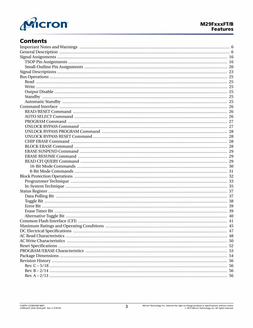
ContentsImportant Notes and Warnings ......................................................................................................................... 6General Description ......................................................................................................................................... 6Signal Assignments ......................................................................................................................................... 16
TSOP Pin Assignments ................................................................................................................................ 16Small-Outline Pin Assignments ................................................................................................................... 20
Signal Descriptions ......................................................................................................................................... 23Bus Operations ............................................................................................................................................... 25
Read .......................................................................................................................................................... 25Write .......................................................................................................................................................... 25Output Disable ........................................................................................................................................... 25Standby ..................................................................................................................................................... 25Automatic Standby ..................................................................................................................................... 25
Command Interface ....................................................................................................................................... 26READ/RESET Command ............................................................................................................................ 26AUTO SELECT Command ........................................................................................................................... 26PROGRAM Command ................................................................................................................................ 27UNLOCK BYPASS Command ...................................................................................................................... 27UNLOCK BYPASS PROGRAM Command ..................................................................................................... 28UNLOCK BYPASS RESET Command ............................................................................................................ 28CHIP ERASE Command .............................................................................................................................. 28BLOCK ERASE Command ........................................................................................................................... 28ERASE SUSPEND Command ....................................................................................................................... 29ERASE RESUME Command ........................................................................................................................ 29READ CFI QUERY Command ...................................................................................................................... 29
16-Bit Mode Commands ......................................................................................................................... 308-Bit Mode Commands ........................................................................................................................... 31
Block Protection Operations ........................................................................................................................... 32Programmer Technique .............................................................................................................................. 33In-System Technique .................................................................................................................................. 35
Status Register ................................................................................................................................................ 37Data Polling Bit .......................................................................................................................................... 37Toggle Bit ................................................................................................................................................... 38Error Bit ..................................................................................................................................................... 39Erase Timer Bit ........................................................................................................................................... 39Alternative Toggle Bit .................................................................................................................................. 40
Common Flash Interface (CFI) ........................................................................................................................ 41Maximum Ratings and Operating Conditions .................................................................................................. 45DC Electrical Specifications ............................................................................................................................ 47AC Read Characteristics .................................................................................................................................. 48AC Write Characteristics ................................................................................................................................. 50Reset Specifications ........................................................................................................................................ 52PROGRAM/ERASE Characteristics .................................................................................................................. 53Package Dimensions ....................................................................................................................................... 54Revision History ............................................................................................................................................. 56
Rev. C – 5/18 ............................................................................................................................................... 56Rev. B – 2/14 ............................................................................................................................................... 56Rev. A – 2/13 ............................................................................................................................................... 56
M29FxxxFT/BFeatures
CCMTD-1725822587-8401m29fxxxf/t_2mb-16mb.pdf - Rev. C 5/18 EN 3 Micron Technology, Inc. reserves the right to change products or specifications without notice.
© 2013 Micron Technology, Inc. All rights reserved.

List of FiguresFigure 1: Logic Diagram ................................................................................................................................... 7Figure 2: Block Addresses, M29F160 (x8) .......................................................................................................... 7Figure 3: Block Addresses, M29F160 (x16) ......................................................................................................... 9Figure 4: Block Addresses, M29F800 (x8) ........................................................................................................ 10Figure 5: Block Addresses, M29F800 (x16) ....................................................................................................... 11Figure 6: Block Addresses, M29F400 (x8) ........................................................................................................ 12Figure 7: Block Addresses, M29F400 (x16) ....................................................................................................... 13Figure 8: Block Addresses, M29F200 (x8) ........................................................................................................ 14Figure 9: Block Addresses, M29F200 (x16) ....................................................................................................... 15Figure 10: M29F160F ..................................................................................................................................... 16Figure 11: M29F800F ..................................................................................................................................... 17Figure 12: M29F400F ..................................................................................................................................... 18Figure 13: M29F200F ..................................................................................................................................... 19Figure 14: M29F800 ....................................................................................................................................... 20Figure 15: M29F400 ....................................................................................................................................... 21Figure 16: M29F200 ....................................................................................................................................... 22Figure 17: Block Protect Flowchart – Programmer Equipment ......................................................................... 33Figure 18: Chip Unprotect Flowchart – Programmer Equipment ..................................................................... 34Figure 19: Block Protect Flowchart – In-System Equipment ............................................................................. 35Figure 20: Chip Protection Flowchart – In-System Equipment ......................................................................... 36Figure 21: Data Polling Flowchart ................................................................................................................... 38Figure 22: Data Toggle Flowchart ................................................................................................................... 39Figure 23: AC Measurement I/O Waveform ..................................................................................................... 45Figure 24: AC Measurement Load Circuit ....................................................................................................... 46Figure 25: Read Mode AC Waveforms ............................................................................................................. 48Figure 26: Write AC Waveforms, Write Enable Controlled ................................................................................ 50Figure 27: Write AC Waveforms, Chip Enable Controlled ................................................................................. 51Figure 28: Reset/Block Temporary Unprotect AC Waveforms ........................................................................... 52Figure 29: 48-Lead TSOP – 12mm x 20mm ...................................................................................................... 54Figure 30: 44-Lead Small-Outline – 500 Mil ..................................................................................................... 55
M29FxxxFT/BFeatures
CCMTD-1725822587-8401m29fxxxf/t_2mb-16mb.pdf - Rev. C 5/18 EN 4 Micron Technology, Inc. reserves the right to change products or specifications without notice.
© 2013 Micron Technology, Inc. All rights reserved.
List of TablesTable 1: Part Number Information ................................................................................................................... 2Table 2: Signal Descriptions ........................................................................................................................... 23Table 3: Bus Operations ................................................................................................................................. 25Table 4: Read Electronic Signature ................................................................................................................. 27Table 5: 16-Bit Mode Commands (BYTE# = HIGH) .......................................................................................... 30Table 6: 8-Bit Mode Commands (BYTE# = LOW) ............................................................................................. 31Table 7: Block and Chip Protection Signal Settings .......................................................................................... 32Table 8: Status Register Bits ........................................................................................................................... 37Table 9: Query Structure Overview ................................................................................................................. 41Table 10: CFI Query Identification String ........................................................................................................ 41Table 11: CFI Query System Interface Information .......................................................................................... 42Table 12: Device Geometry Definition ............................................................................................................ 42Table 13: Primary Algorithm-Specific Extended Query Table ........................................................................... 43Table 14: Security Code Area .......................................................................................................................... 44Table 15: Absolute Maximum Ratings ............................................................................................................. 45Table 16: Operating and AC Measurement Conditions .................................................................................... 45Table 17: Device Capacitance ........................................................................................................................ 46Table 18: DC Characteristics .......................................................................................................................... 47Table 19: Read AC Characteristics .................................................................................................................. 48Table 20: Write AC Characteristics, Write Enable Controlled ............................................................................ 50Table 21: Write AC Characteristics, Chip Enable Controlled ............................................................................. 51Table 22: Reset/Block Temporary Unprotect AC Characteristics ...................................................................... 52Table 23: Program/Erase Characteristics ........................................................................................................ 53
M29FxxxFT/BFeatures
CCMTD-1725822587-8401m29fxxxf/t_2mb-16mb.pdf - Rev. C 5/18 EN 5 Micron Technology, Inc. reserves the right to change products or specifications without notice.
© 2013 Micron Technology, Inc. All rights reserved.
Important Notes and WarningsMicron Technology, Inc. ("Micron") reserves the right to make changes to information published in this document,including without limitation specifications and product descriptions. This document supersedes and replaces allinformation supplied prior to the publication hereof. You may not rely on any information set forth in this docu-ment if you obtain the product described herein from any unauthorized distributor or other source not authorizedby Micron.
Automotive Applications. Products are not designed or intended for use in automotive applications unless specifi-cally designated by Micron as automotive-grade by their respective data sheets. Distributor and customer/distrib-utor shall assume the sole risk and liability for and shall indemnify and hold Micron harmless against all claims,costs, damages, and expenses and reasonable attorneys' fees arising out of, directly or indirectly, any claim ofproduct liability, personal injury, death, or property damage resulting directly or indirectly from any use of non-automotive-grade products in automotive applications. Customer/distributor shall ensure that the terms and con-ditions of sale between customer/distributor and any customer of distributor/customer (1) state that Micronproducts are not designed or intended for use in automotive applications unless specifically designated by Micronas automotive-grade by their respective data sheets and (2) require such customer of distributor/customer to in-demnify and hold Micron harmless against all claims, costs, damages, and expenses and reasonable attorneys'fees arising out of, directly or indirectly, any claim of product liability, personal injury, death, or property damageresulting from any use of non-automotive-grade products in automotive applications.
Critical Applications. Products are not authorized for use in applications in which failure of the Micron compo-nent could result, directly or indirectly in death, personal injury, or severe property or environmental damage("Critical Applications"). Customer must protect against death, personal injury, and severe property and environ-mental damage by incorporating safety design measures into customer's applications to ensure that failure of theMicron component will not result in such harms. Should customer or distributor purchase, use, or sell any Microncomponent for any critical application, customer and distributor shall indemnify and hold harmless Micron andits subsidiaries, subcontractors, and affiliates and the directors, officers, and employees of each against all claims,costs, damages, and expenses and reasonable attorneys' fees arising out of, directly or indirectly, any claim ofproduct liability, personal injury, or death arising in any way out of such critical application, whether or not Mi-cron or its subsidiaries, subcontractors, or affiliates were negligent in the design, manufacture, or warning of theMicron product.
Customer Responsibility. Customers are responsible for the design, manufacture, and operation of their systems,applications, and products using Micron products. ALL SEMICONDUCTOR PRODUCTS HAVE INHERENT FAIL-URE RATES AND LIMITED USEFUL LIVES. IT IS THE CUSTOMER'S SOLE RESPONSIBILITY TO DETERMINEWHETHER THE MICRON PRODUCT IS SUITABLE AND FIT FOR THE CUSTOMER'S SYSTEM, APPLICATION, ORPRODUCT. Customers must ensure that adequate design, manufacturing, and operating safeguards are includedin customer's applications and products to eliminate the risk that personal injury, death, or severe property or en-vironmental damages will result from failure of any semiconductor component.
Limited Warranty. In no event shall Micron be liable for any indirect, incidental, punitive, special or consequentialdamages (including without limitation lost profits, lost savings, business interruption, costs related to the removalor replacement of any products or rework charges) whether or not such damages are based on tort, warranty,breach of contract or other legal theory, unless explicitly stated in a written agreement executed by Micron's dulyauthorized representative.
General Description
This description applies specifically to the M29F 16Mb (2 Meg x 8 or 1 Meg x 16) nonvo-latile memory device, but also applies to lower densities. The device enables READ,ERASE, and PROGRAM operations using a single, low-voltage (4.5–5.5V) supply. On
M29FxxxFT/BImportant Notes and Warnings
CCMTD-1725822587-8401m29fxxxf/t_2mb-16mb.pdf - Rev. C 5/18 EN 6 Micron Technology, Inc. reserves the right to change products or specifications without notice.
© 2013 Micron Technology, Inc. All rights reserved.

power-up, the device defaults to read mode and can be read in the same way as a ROMor EPROM.
The device is divided into blocks that can be erased independently, preserving valid da-ta while old data is erased. Each block can be protected independently to prevent acci-dental PROGRAM or ERASE operations from modifying the memory. PROGRAM andERASE commands are written to the command interface. An on-chip program/erasecontroller simplifies the process of programming or erasing the device by managing theoperations required to update the memory contents.
The end of a PROGRAM or ERASE operation can be detected and any error conditionsidentified. The command set required to control the memory is consistent with JEDECstandards.
The blocks are asymmetrically arranged. The first or last 64KB have been divided intofour additional blocks. The 16KB boot block can be used for small initialization code tostart the microprocessor. The two 8KB parameter blocks can be used for parameterstorage. The remaining 32KB is a small main block where the application may be stored.
CE#, OE#, and WE# control the bus operation of the memory. They enable simple con-nection to most microprocessors, often without additional logic. Devices are offered in48-pin TSOP (12mm x 20mm) and 44-pin small-outline packages. The device is sup-plied with all the bits erased (set to 1).
Figure 1: Logic Diagram
20
A[19:0]
WE#
DQ[7:0]
DQ[14:8]
VCC
CE#
VSS
15
OE#
RST#
DQ15/A–1
RY/BY#
BYTE#
Figure 2: Block Addresses, M29F160 (x8)
M29FxxxFT/BGeneral Description
CCMTD-1725822587-8401m29fxxxf/t_2mb-16mb.pdf - Rev. C 5/18 EN 7 Micron Technology, Inc. reserves the right to change products or specifications without notice.
© 2013 Micron Technology, Inc. All rights reserved.

1FFFFFh
1FC000h
01FFFFh
010000h00FFFFh
000000h
1F7FFFh
1F0000h
1E0000h
1EFFFFh
Total of 3164 KB blocks
1FFFFFh
1F0000h
003FFFh
000000h
1EFFFFh
01FFFFh
1E0000h
010000h
Total of 3164 KB blocks
00FFFFh
008000h
1FBFFFh
1FA000h1F9FFFh
1F8000h
007FFFh
006000h005FFFh
004000h
16KB
64KB
64KB
Top boot block addresses (x8)
32KB
64KB
16KB
64KB
64KB
Bottom boot block addresses (x8)
32KB
64KB
8KB
8KB
8KB
8KB
M29FxxxFT/BGeneral Description
CCMTD-1725822587-8401m29fxxxf/t_2mb-16mb.pdf - Rev. C 5/18 EN 8 Micron Technology, Inc. reserves the right to change products or specifications without notice.
© 2013 Micron Technology, Inc. All rights reserved.

Figure 3: Block Addresses, M29F160 (x16)
FFFFFh
FE000h
0FFFFh
08000h07FFFh
00000h
FBFFFh
F8000h
F0000h
F7FFFh
Total of 3132 Kword blocks
FFFFFh
F8000h
01FFFh
00000h
F7FFFh
0FFFFh
F0000h
08000h
Total of 3132 Kword blocks
07FFFh
04000h
FDFFFh
FD000hFCFFFh
FC000h
03FFFh
03000h02FFFh
02000h
8 Kword
32 Kword
32 Kword
16 Kword
32 Kword
8 Kword
32 Kword
32 Kword
16 Kword
32 Kword
4 Kword
4 Kword
4 Kword
4 Kword
Top boot block addresses (x16) Bottom boot block addresses (x16)
M29FxxxFT/BGeneral Description
CCMTD-1725822587-8401m29fxxxf/t_2mb-16mb.pdf - Rev. C 5/18 EN 9 Micron Technology, Inc. reserves the right to change products or specifications without notice.
© 2013 Micron Technology, Inc. All rights reserved.
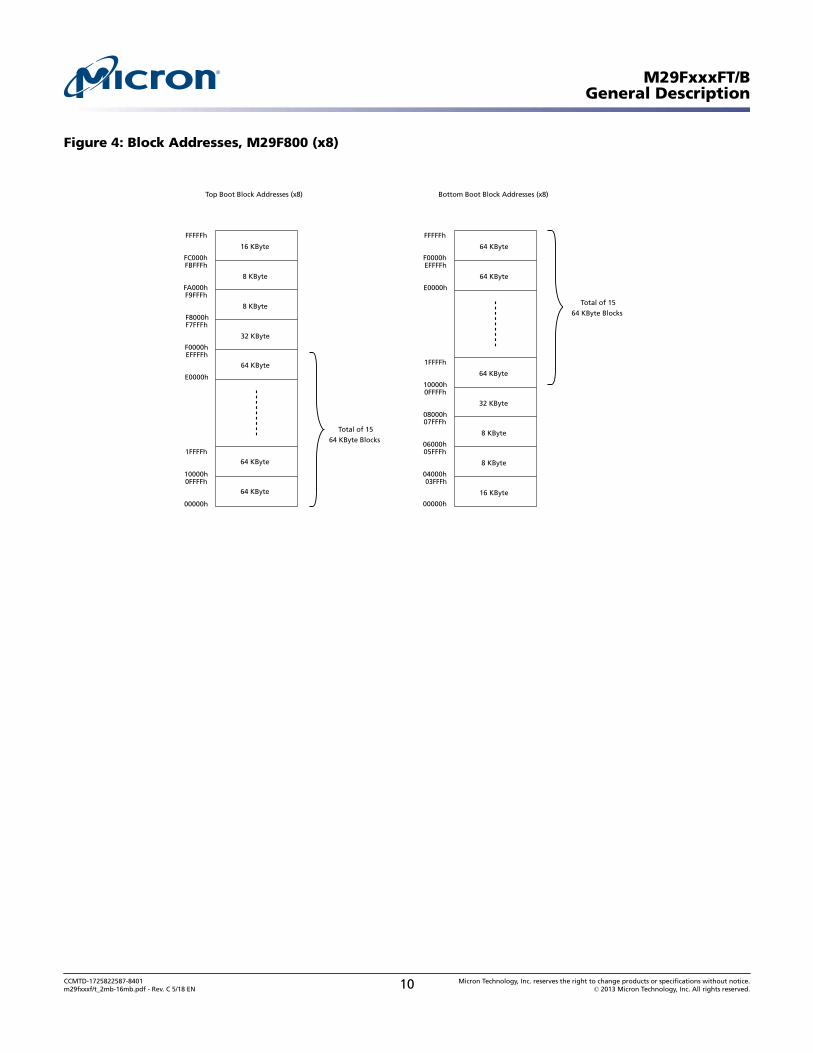
Figure 4: Block Addresses, M29F800 (x8)
16 KByte
FFFFFh
FC000h
64 KByte1FFFFh
10000h
64 KByte0FFFFh
00000h
Top Boot Block Addresses (x8)
32 KByte
F7FFFh
F0000h
64 KByte
E0000h
EFFFFh
Total of 15
64 KByte Blocks
16 KByte
FFFFFh
F0000h
64 KByte
64 KByte
03FFFh
00000h
Bottom Boot Block Addresses (x8)
32 KByte
EFFFFh
1FFFFh
64 KByte
E0000h
10000h
Total of 15
64 KByte Blocks
0FFFFh
08000h
8 KByte
8 KByte
FBFFFh
FA000hF9FFFh
F8000h
8 KByte
8 KByte
07FFFh
06000h05FFFh
04000h
M29FxxxFT/BGeneral Description
CCMTD-1725822587-8401m29fxxxf/t_2mb-16mb.pdf - Rev. C 5/18 EN 10 Micron Technology, Inc. reserves the right to change products or specifications without notice.
© 2013 Micron Technology, Inc. All rights reserved.

Figure 5: Block Addresses, M29F800 (x16)
8 Kword
7FFFFh
7E000h
32 Kword0FFFFh
08000h
32 Kword07FFFh
00000h
16 Kword
7BFFFh
78000h
32 Kword
70000h
77FFFh
Total of 1532 Kword blocks
8 Kword
7FFFFh
78000h
32 Kword
32 Kword
01FFFh
00000h
16 Kword
77FFFh
0FFFFh
32 Kword
70000h
08000h
Total of 1532 Kword blocks
07FFFh
04000h
4 Kword
4 Kword
7DFFFh
7D000h7CFFFh
7C000h
4 Kword
4 Kword
03FFFh
03000h02FFFh
02000h
Top boot block addresses (x16) Bottom boot block addresses (x16)
M29FxxxFT/BGeneral Description
CCMTD-1725822587-8401m29fxxxf/t_2mb-16mb.pdf - Rev. C 5/18 EN 11 Micron Technology, Inc. reserves the right to change products or specifications without notice.
© 2013 Micron Technology, Inc. All rights reserved.
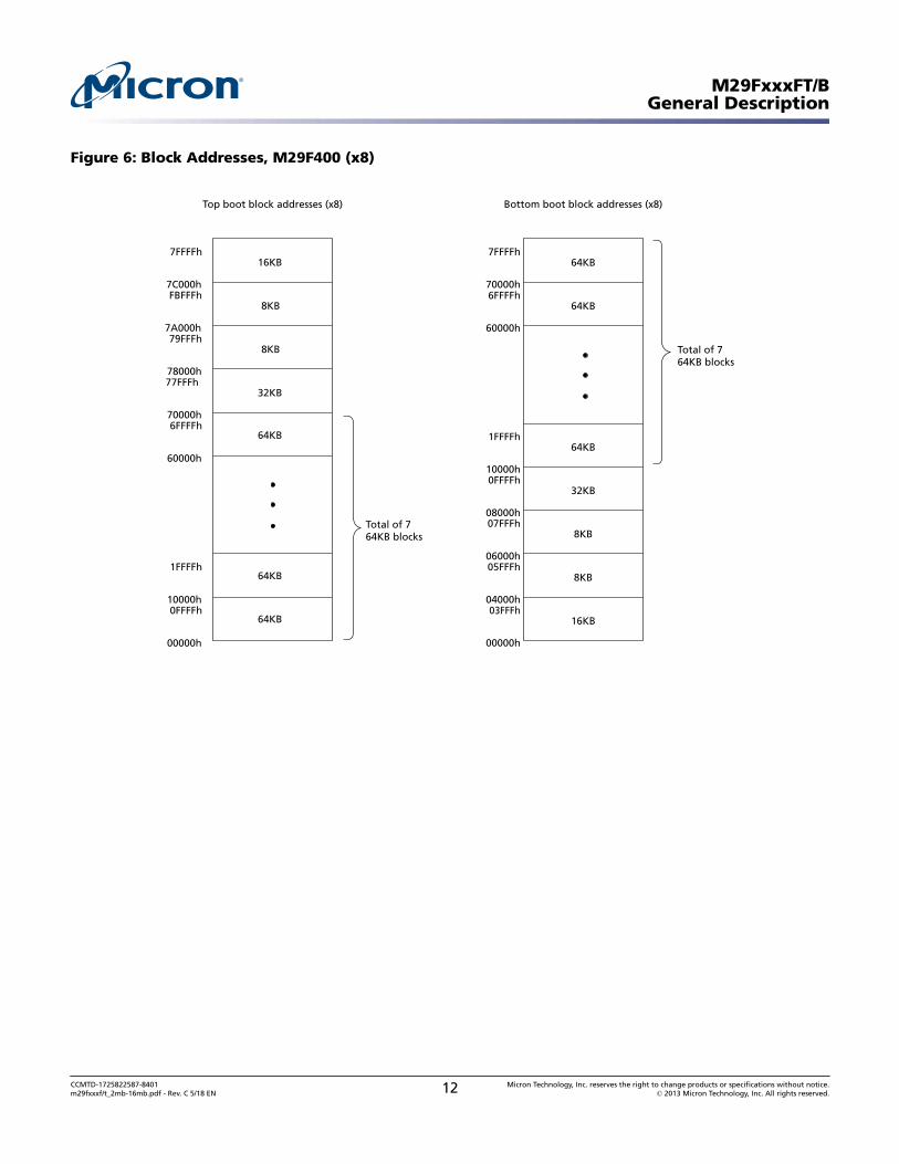
Figure 6: Block Addresses, M29F400 (x8)
7FFFFh
7C000h
1FFFFh
10000h0FFFFh
00000h
77FFFh
70000h
60000h
6FFFFh
Total of 764KB blocks
7FFFFh
70000h
03FFFh
00000h
6FFFFh
1FFFFh
60000h
10000h
Total of 764KB blocks
0FFFFh
08000h
FBFFFh
7A000h79FFFh
78000h
07FFFh
06000h05FFFh
04000h
16KB
64KB
64KB
Top boot block addresses (x8)
32KB
64KB
16KB
64KB
64KB
Bottom boot block addresses (x8)
32KB
64KB
8KB
8KB
8KB
8KB
M29FxxxFT/BGeneral Description
CCMTD-1725822587-8401m29fxxxf/t_2mb-16mb.pdf - Rev. C 5/18 EN 12 Micron Technology, Inc. reserves the right to change products or specifications without notice.
© 2013 Micron Technology, Inc. All rights reserved.
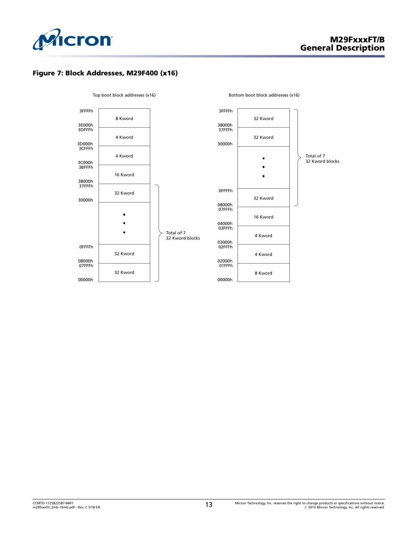
Figure 7: Block Addresses, M29F400 (x16)
3FFFFh
3E000h
0FFFFh
08000h07FFFh
00000h
3BFFFh
38000h
30000h
37FFFh
Total of 732 Kword blocks
3FFFFh
38000h
01FFFh
00000h
37FFFh
0FFFFh
30000h
08000h
Total of 732 Kword blocks
07FFFh
04000h
3DFFFh
3D000h3CFFFh
3C000h
03FFFh
03000h02FFFh
02000h
8 Kword
32 Kword
32 Kword
Top boot block addresses (x16)
16 Kword
32 Kword
8 Kword
32 Kword
32 Kword
Bottom boot block addresses (x16)
16 Kword
32 Kword
4 Kword
4 Kword
4 Kword
4 Kword
M29FxxxFT/BGeneral Description
CCMTD-1725822587-8401m29fxxxf/t_2mb-16mb.pdf - Rev. C 5/18 EN 13 Micron Technology, Inc. reserves the right to change products or specifications without notice.
© 2013 Micron Technology, Inc. All rights reserved.

Figure 8: Block Addresses, M29F200 (x8)
16KB
3FFFFh
3C000h
64KB1FFFFh
10000h
64KB0FFFFh
00000h
Top boot block addresses (x8)
32KB
37FFFh
30000h
64KB
20000h
3FFFFh
Total of 364KB blocks
16KB
2FFFFh
20000h
64KB
64KB
03FFFh
00000h
Bottom boot block addresses (x8)
32KB
2FFFFh
1FFFFh
64KB
20000h
10000h
Total of 364KB blocks
0FFFFh
08000h
8KB
8KB
3BFFFh
3A000h39FFFh
38000h
8KB
8KB
07FFFh
06000h05FFFh
04000h
M29FxxxFT/BGeneral Description
CCMTD-1725822587-8401m29fxxxf/t_2mb-16mb.pdf - Rev. C 5/18 EN 14 Micron Technology, Inc. reserves the right to change products or specifications without notice.
© 2013 Micron Technology, Inc. All rights reserved.

Figure 9: Block Addresses, M29F200 (x16)
8 Kword
1FFFFh
1E000h
32 Kword0FFFFh
08000h
32 Kword07FFFh
00000h
Top boot block addresses (x16)
16 Kword
3BFFFh
18000h
32 Kword
10000h
17FFFh
Total of 332 Kword blocks
8 Kword
1FFFFh
18000h
32 Kword
32 Kword
01FFFh
00000h
Bottom boot block addresses (x16)
16 Kword
17FFFh
0FFFFh
32 Kword
10000h
08000h
Total of 332 Kword blocks
07FFFh
04000h
4 Kword
4 Kword
1DFFFh
1D000h3CFFFh
1C000h
4 Kword
4 Kword
03FFFh
03000h02FFFh
02000h
M29FxxxFT/BGeneral Description
CCMTD-1725822587-8401m29fxxxf/t_2mb-16mb.pdf - Rev. C 5/18 EN 15 Micron Technology, Inc. reserves the right to change products or specifications without notice.
© 2013 Micron Technology, Inc. All rights reserved.

Signal Assignments
TSOP Pin Assignments
Figure 10: M29F160F
DQ3
DQ9DQ2
A6DQ0
WE#
A3
R/B#
DQ6A8A9
DQ13
A17
A10 DQ14
A2
DQ12
DQ10
DQ15A–1
VCC
DQ4
DQ5
A7
DQ7
NCNC
AI06850_160
12
1
13
24 25
3637
48
DQ8
NCA19
A1
A18
A4A5
DQ1
DQ11
OE#
A12A13
A16
A11
BYTE#A15A14
VSS
CE#A0
RP#
VSS
M29FxxxFT/BSignal Assignments
CCMTD-1725822587-8401m29fxxxf/t_2mb-16mb.pdf - Rev. C 5/18 EN 16 Micron Technology, Inc. reserves the right to change products or specifications without notice.
© 2013 Micron Technology, Inc. All rights reserved.

Figure 11: M29F800F
DQ3
DQ9DQ2
A6DQ0
WE#
A3
R/B#
DQ6A8A9
DQ13
A17
A10 DQ14
A2
DQ12
DQ10
DQ15A–1
VCC
DQ4
DQ5
A7
DQ7
NCNC
AI06850_800
12
1
13
24 25
3637
48
DQ8
NC
A1
A18
A4A5
DQ1
DQ11
OE#
A12A13
A16
A11
BYTE#A15A14
VSS
CE#A0
RP#
VSS
NC
M29FxxxFT/BSignal Assignments
CCMTD-1725822587-8401m29fxxxf/t_2mb-16mb.pdf - Rev. C 5/18 EN 17 Micron Technology, Inc. reserves the right to change products or specifications without notice.
© 2013 Micron Technology, Inc. All rights reserved.
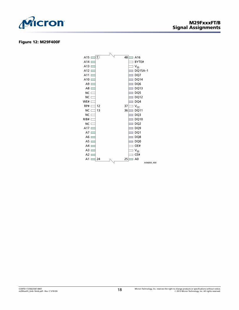
Figure 12: M29F400F
DQ3
DQ9DQ2
A6DQ0
WE#
A3
R/B#
DQ6A8A9
DQ13
A17
A10 DQ14
A2
DQ12
DQ10
DQ15A–1
VCC
DQ4
DQ5
A7
DQ7
NCNC
AI06850_400
12
1
13
24 25
3637
48
DQ8
NC
A1
A4A5
DQ1
DQ11
OE#
A12A13
A16
A11
BYTE#A15A14
VSS
CE#A0
RP#
VSS
NC
NC
M29FxxxFT/BSignal Assignments
CCMTD-1725822587-8401m29fxxxf/t_2mb-16mb.pdf - Rev. C 5/18 EN 18 Micron Technology, Inc. reserves the right to change products or specifications without notice.
© 2013 Micron Technology, Inc. All rights reserved.
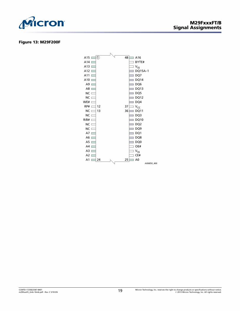
Figure 13: M29F200F
DQ3
DQ9DQ2
A6DQ0
WE#
A3
R/B#
DQ6A8A9
DQ13
A10 DQ14
A2
DQ12
DQ10
DQ15A–1
VCC
DQ4
DQ5
A7
DQ7
NCNC
AI06850_400
12
1
13
24 25
3637
48
DQ8
NC
A1
A4A5
DQ1
DQ11
OE#
A12A13
A16
A11
BYTE#A15A14
VSS
CE#A0
RP#
VSS
NC
NCNC
M29FxxxFT/BSignal Assignments
CCMTD-1725822587-8401m29fxxxf/t_2mb-16mb.pdf - Rev. C 5/18 EN 19 Micron Technology, Inc. reserves the right to change products or specifications without notice.
© 2013 Micron Technology, Inc. All rights reserved.

Small-Outline Pin Assignments
Figure 14: M29F800
DQ3
DQ9DQ2
DQ0
A8A9
DQ6DQ13
A17
DQ12DQ10
DQ15A–1
VCC
DQ4
DQ5
DQ14DQ7
AI02906_800
1
1112
22 23
3334
44
DQ8
A6
A3A2
A7
A1
A4A5
DQ1
DQ11
OE#
WE#
BYTE#
A10
A16
A12A13
A11
A15A14
VSS
A0
RP#R/B#
VSS
CE#
A18
M29FxxxFT/BSignal Assignments
CCMTD-1725822587-8401m29fxxxf/t_2mb-16mb.pdf - Rev. C 5/18 EN 20 Micron Technology, Inc. reserves the right to change products or specifications without notice.
© 2013 Micron Technology, Inc. All rights reserved.

Figure 15: M29F400
DQ3
DQ9DQ2
DQ0
A8A9
DQ6DQ13
A17
DQ12DQ10
DQ15A–1
VCC
DQ4
DQ5
DQ14DQ7
AI02906_400
1
1112
22 23
3334
44
DQ8
A6
A3A2
A7
A1
A4A5
DQ1
DQ11
OE#
WE#
BYTE#
A10
A16
A12A13
A11
A15A14
VSS
A0
RP#R/B#
VSS
CE#
NC
M29FxxxFT/BSignal Assignments
CCMTD-1725822587-8401m29fxxxf/t_2mb-16mb.pdf - Rev. C 5/18 EN 21 Micron Technology, Inc. reserves the right to change products or specifications without notice.
© 2013 Micron Technology, Inc. All rights reserved.
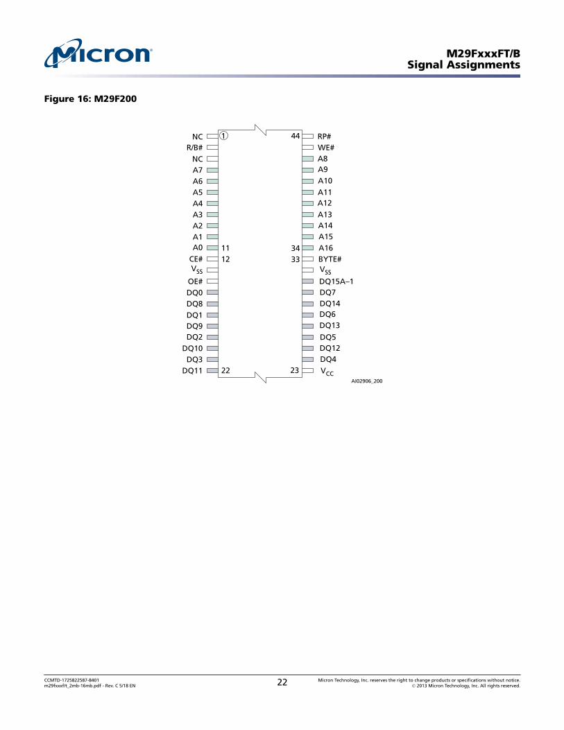
Figure 16: M29F200
DQ3
DQ9DQ2
DQ0
A8A9
DQ6DQ13
DQ12DQ10
DQ15A–1
VCC
DQ4
DQ5
DQ14DQ7
AI02906_200
1
1112
22 23
3334
44
DQ8
A6
A3A2
A7
A1
A4A5
DQ1
DQ11
OE#
WE#
BYTE#
A10
A16
A12A13
A11
A15A14
VSS
A0
RP#R/B#
VSS
CE#
NC
NC
M29FxxxFT/BSignal Assignments
CCMTD-1725822587-8401m29fxxxf/t_2mb-16mb.pdf - Rev. C 5/18 EN 22 Micron Technology, Inc. reserves the right to change products or specifications without notice.
© 2013 Micron Technology, Inc. All rights reserved.

Signal DescriptionsThe signal description table below is a comprehensive list of signals for this device fami-ly. All signals listed may not be supported on this device. See Signal Assignments for in-formation specific to this device.
Table 2: Signal Descriptions
Name Type Description
A[MAX:0] Input Address: Selects the cells in the array to access during READ operations. During WRITE oper-ations, they control the commands sent to the command interface of the program/erase con-troller.
CE# Input Chip enable: Activates the device, enabling READ and WRITE operations to be performed.When CE# is HIGH, all other pins are ignored.
OE# Input Output enable: Controls the bus READ operation.
WE# Input Write enable: Controls the bus WRITE operation of the command interface.
BYTE# Input Byte/word organization select: Switches between x8 and x16 bus modes. When BYTE# isLOW, the device is in x8 mode; when HIGH, the device is in x16 mode.
RST# Input Reset: Applies a hardware reset to the device, which is achieved by holding RST# LOW for atleast tPLPX. After RST# goes HIGH, the device is ready for READ and WRITE operations (aftertPHEL or tRHEL, whichever occurs last).Holding RST# at VID will temporarily unprotect the protected blocks. PROGRAM and ERASEoperations on all blocks will then be possible. The transition from VIH to VID must be slowerthan tPHPHH.
DQ[7:0] I/O Data I/O: Outputs the data stored at the selected address during a READ operation. DuringWRITE operations, they represent the commands sent to the command interface of the pro-gram/erase controller.
DQ[14:8] I/O Data I/O: Outputs the data stored at the selected address during a READ operation whenBYTE# is HIGH. When BYTE# is LOW, these pins are not used and are High-Z. During WRITEoperations, these bits are not used. When reading the status register, these bits should be ig-nored.
DQ15/A-1 I/O Data I/O or address input: When the device operates in x16 bus mode, this pin behaves asdata I/O, together with DQ[14:8]. When the device operates in x8 bus mode, this pin behavesas the least significant bit of the address.Except where stated explicitly otherwise, DQ15 = data I/O (x16 mode); A-1 = address input (x8mode).
RY/BY# Output Ready busy: Open-drain output that can be used to identify when the device is performinga PROGRAM or ERASE operation. During PROGRAM or ERASE operations, RY/BY# is LOW,and is High-Z during read mode, auto select mode, and erase suspend mode. After a hard-ware reset, READ and WRITE operations cannot begin until RY/BY# goes High-Z (see RESETAC Specifications for more details).The use of an open-drain output enables the RY/BY# pins from several devices to be connec-ted to a single pull-up resistor to VCCQ. A low value will then indicate that one (or more) ofthe devices is (are) busy.
M29FxxxFT/BSignal Descriptions
CCMTD-1725822587-8401m29fxxxf/t_2mb-16mb.pdf - Rev. C 5/18 EN 23 Micron Technology, Inc. reserves the right to change products or specifications without notice.
© 2013 Micron Technology, Inc. All rights reserved.
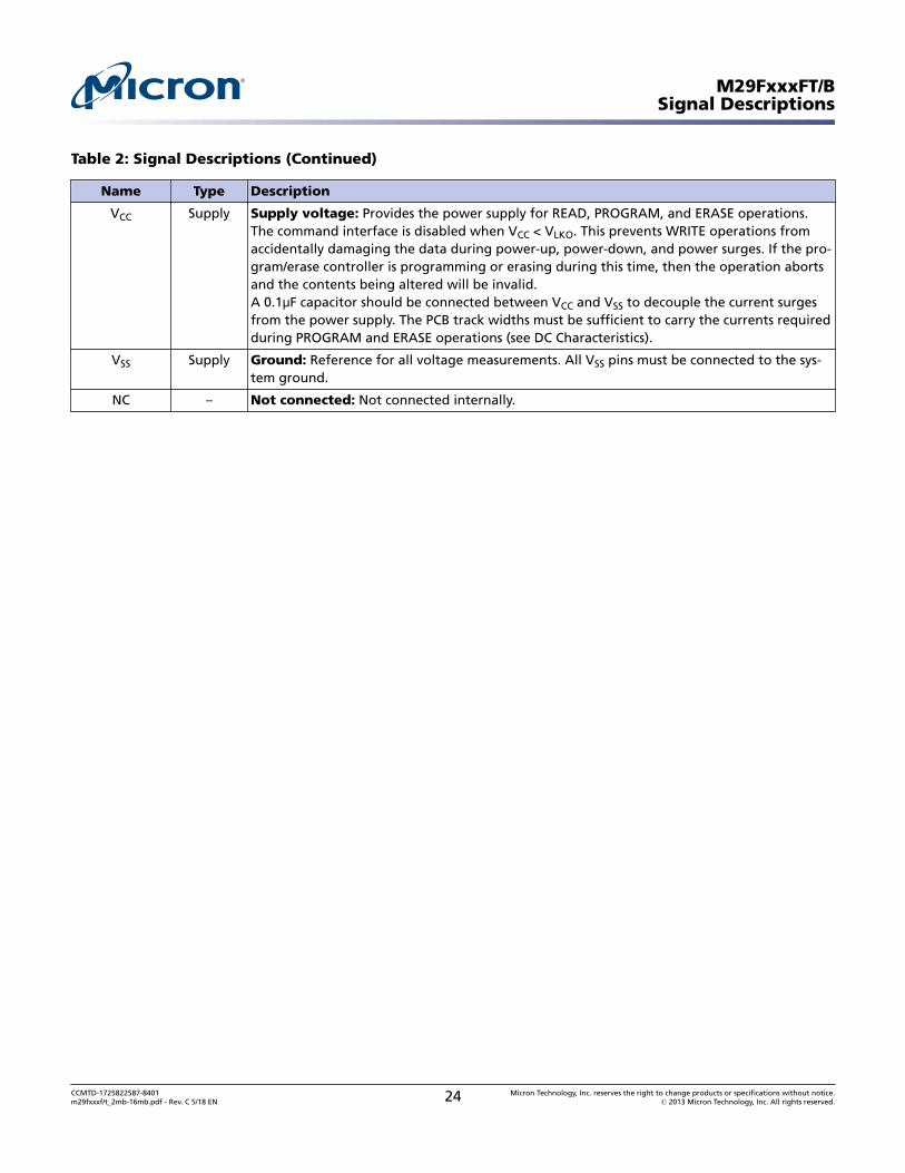
Table 2: Signal Descriptions (Continued)
Name Type Description
VCC Supply Supply voltage: Provides the power supply for READ, PROGRAM, and ERASE operations.The command interface is disabled when VCC < VLKO. This prevents WRITE operations fromaccidentally damaging the data during power-up, power-down, and power surges. If the pro-gram/erase controller is programming or erasing during this time, then the operation abortsand the contents being altered will be invalid.A 0.1μF capacitor should be connected between VCC and VSS to decouple the current surgesfrom the power supply. The PCB track widths must be sufficient to carry the currents requiredduring PROGRAM and ERASE operations (see DC Characteristics).
VSS Supply Ground: Reference for all voltage measurements. All VSS pins must be connected to the sys-tem ground.
NC – Not connected: Not connected internally.
M29FxxxFT/BSignal Descriptions
CCMTD-1725822587-8401m29fxxxf/t_2mb-16mb.pdf - Rev. C 5/18 EN 24 Micron Technology, Inc. reserves the right to change products or specifications without notice.
© 2013 Micron Technology, Inc. All rights reserved.

Bus Operations
Table 3: Bus Operations
Notes 1 through 2 apply to entire table
Operation CE# OE# WE#
8-Bit Mode 16-Bit Mode
A[MAX:0],DQ15/A-1 DQ[14:8] DQ[7:0] A[MAX:0]
DQ15/A-1,DQ[14:0]
READ L L H Cell address High-Z Data output Cell address Data output
WRITE L H L Command address High-Z Data input Command address Data input
OUTPUTDISABLE
X H H X High-Z High-Z X High-Z
STANDBY H X X X High-Z High-Z X High-Z
Notes: 1. H = Logic level HIGH (VIH); L = Logic level LOW (VIL); X = HIGH or LOW.2. Typically glitches of less than 5ns on Chip Enable or Write Enable are ignored by the
memory and do not affect bus operations.
Read
Bus READ operations read from the memory cells or specific registers in the commandinterface. A valid bus READ operation involves setting the desired address on the ad-dress inputs, taking CE# and OE# LOW, and holding WE# HIGH. The data I/Os will out-put the value. (See AC Characteristics for details about when the output becomes valid.)
Write
Bus WRITE operations write to the command interface. A valid bus WRITE operationbegins by setting the desired address on the address inputs. The address inputs arelatched by the command interface on the falling edge of CE# or WE#, whichever occurslast. The data I/Os are latched by the command interface on the rising edge of CE# orWE#, whichever occurs first. OE# must remain HIGH during the entire bus WRITE oper-ation. (See AC Characteristics for timing requirement details.)
Output Disable
Data I/Os are High-Z when OE# is HIGH.
Standby
When CE# is HIGH, the device enters standby, and data I/Os are High-Z. To reduce thesupply current to the standby supply current (ICC2), CE# must be held within VCC ±0.2V.(See DC Characteristics.) During PROGRAM or ERASE operations the device will contin-ue to use the program/erase supply current (ICC3) until the operation completes.
Automatic Standby
If CMOS levels (VCC ±0.2V) are used to drive the bus, and the bus is inactive for 150ns ormore, the device enters automatic standby, and the internal supply current is reducedto that of the standby supply current, ICC2. The data I/Os will output data if a READ op-eration is in progress.
M29FxxxFT/BBus Operations
CCMTD-1725822587-8401m29fxxxf/t_2mb-16mb.pdf - Rev. C 5/18 EN 25 Micron Technology, Inc. reserves the right to change products or specifications without notice.
© 2013 Micron Technology, Inc. All rights reserved.
Command InterfaceAll WRITE operations are interpreted by the command interface. Commands consist ofone or more sequential WRITE operations. Failure to observe a valid sequence will re-sult in the memory returning to read mode. The long command sequences are imposedto maximize data security.
The address used for the commands changes depending on whether the memory is in16-bit or 8-bit mode.
READ/RESET Command
The READ/RESET command returns the device to read mode, where it behaves like aROM or EPROM, unless otherwise stated. It also resets the errors in the status register.Either one or three WRITE operations can be used to issue the READ/RESET command.
The READ/RESET command can be issued, between WRITE cycles, before the start of aPROGRAM or ERASE operation, to return the device to read mode. Once the PROGRAMor ERASE operation has started, the READ/RESET command is no longer accepted. TheREAD/RESET command will not abort an ERASE operation when issued while in erasesuspend.
AUTO SELECT Command
The AUTO SELECT command is used to read the electronic signature, including themanufacturer code, the device code and the block protection status. Three consecutiveWRITE operations are required to issue the AUTO SELECT command. Once the com-mand is issued, the memory remains in auto select mode until a READ/RESET com-mand is issued. READ CFI QUERY and READ/RESET commands are accepted in autoSelect mode, while all other commands are ignored.
Note: These operations are intended for use by programming equipment and are nottypically used in applications. They require V ID to be applied to some of the pins.
From the auto select mode the manufacturer code can be read using a READ operationwith A0 = VIL and A1 = VIL. The other address bits may be set to either V IL or VIH. Themanufacturer code for Micron is 0001h.
The device code can be read using a READ operation with A0 = VIH and A1 = VIL. Theother address bits may be set to either VIL or VIH.
The block protection status of each block can be read using a READ operation with A0 =VIL, A1 = VIH, and A12-A19 specifying the address of the block. The other address bitsmay be set to either VIL or VIH. If the addressed block is protected then 01h is output onData Inputs/Outputs DQ0-DQ7, otherwise 00h is output. See Block Protection Opera-tions for information on the block protection status; the Programmer Technique BlockProtection table includes block protection bus READ information.
M29FxxxFT/BCommand Interface
CCMTD-1725822587-8401m29fxxxf/t_2mb-16mb.pdf - Rev. C 5/18 EN 26 Micron Technology, Inc. reserves the right to change products or specifications without notice.
© 2013 Micron Technology, Inc. All rights reserved.
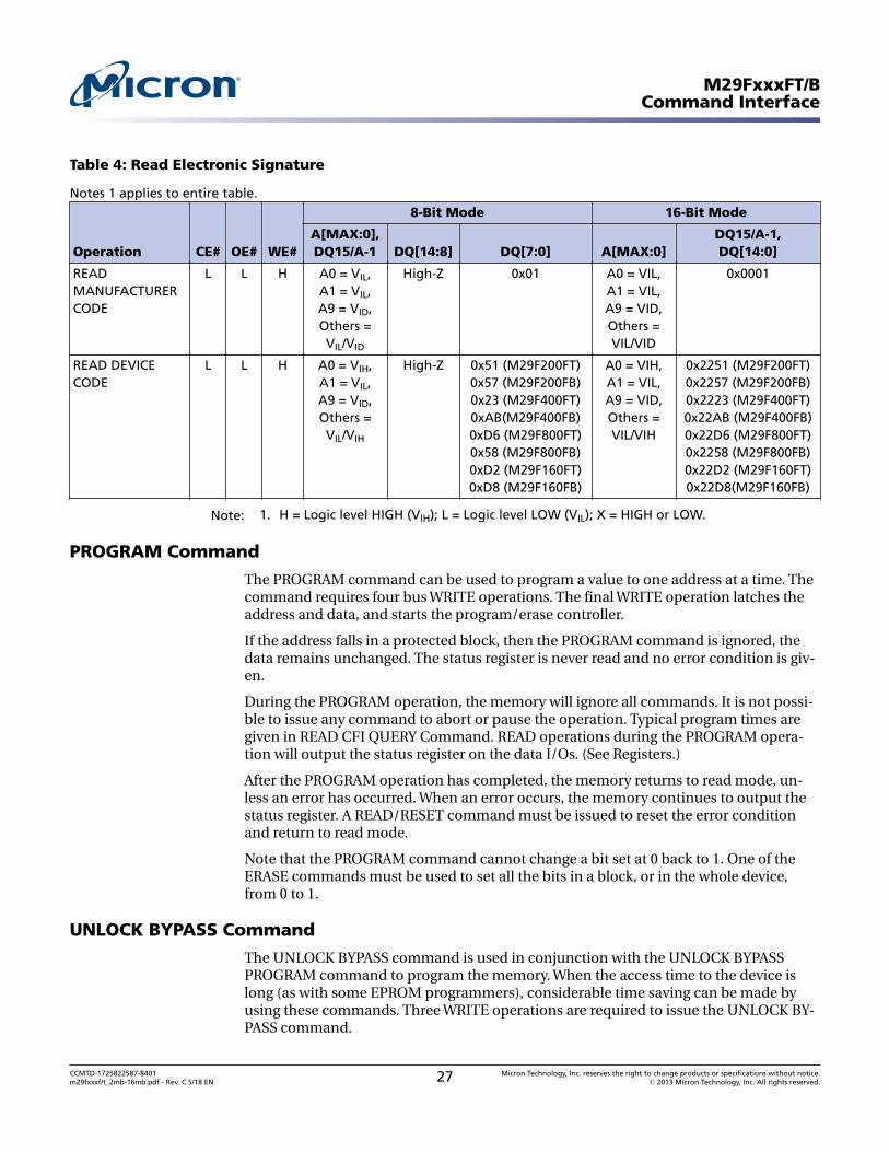
Table 4: Read Electronic Signature
Notes 1 applies to entire table.
Operation CE# OE# WE#
8-Bit Mode 16-Bit Mode
A[MAX:0],DQ15/A-1 DQ[14:8] DQ[7:0] A[MAX:0]
DQ15/A-1,DQ[14:0]
READMANUFACTURERCODE
L L H A0 = VIL,A1 = VIL,A9 = VID,Others =VIL/VID
High-Z 0x01 A0 = VIL,A1 = VIL,A9 = VID,Others =VIL/VID
0x0001
READ DEVICECODE
L L H A0 = VIH,A1 = VIL,A9 = VID,Others =VIL/VIH
High-Z 0x51 (M29F200FT)0x57 (M29F200FB)0x23 (M29F400FT)0xAB(M29F400FB)0xD6 (M29F800FT)0x58 (M29F800FB)0xD2 (M29F160FT)0xD8 (M29F160FB)
A0 = VIH,A1 = VIL,A9 = VID,Others =VIL/VIH
0x2251 (M29F200FT)0x2257 (M29F200FB)0x2223 (M29F400FT)0x22AB (M29F400FB)0x22D6 (M29F800FT)0x2258 (M29F800FB)0x22D2 (M29F160FT)0x22D8(M29F160FB)
Note: 1. H = Logic level HIGH (VIH); L = Logic level LOW (VIL); X = HIGH or LOW.
PROGRAM Command
The PROGRAM command can be used to program a value to one address at a time. Thecommand requires four bus WRITE operations. The final WRITE operation latches theaddress and data, and starts the program/erase controller.
If the address falls in a protected block, then the PROGRAM command is ignored, thedata remains unchanged. The status register is never read and no error condition is giv-en.
During the PROGRAM operation, the memory will ignore all commands. It is not possi-ble to issue any command to abort or pause the operation. Typical program times aregiven in READ CFI QUERY Command. READ operations during the PROGRAM opera-tion will output the status register on the data I/Os. (See Registers.)
After the PROGRAM operation has completed, the memory returns to read mode, un-less an error has occurred. When an error occurs, the memory continues to output thestatus register. A READ/RESET command must be issued to reset the error conditionand return to read mode.
Note that the PROGRAM command cannot change a bit set at 0 back to 1. One of theERASE commands must be used to set all the bits in a block, or in the whole device,from 0 to 1.
UNLOCK BYPASS Command
The UNLOCK BYPASS command is used in conjunction with the UNLOCK BYPASSPROGRAM command to program the memory. When the access time to the device islong (as with some EPROM programmers), considerable time saving can be made byusing these commands. Three WRITE operations are required to issue the UNLOCK BY-PASS command.
M29FxxxFT/BCommand Interface
CCMTD-1725822587-8401m29fxxxf/t_2mb-16mb.pdf - Rev. C 5/18 EN 27 Micron Technology, Inc. reserves the right to change products or specifications without notice.
© 2013 Micron Technology, Inc. All rights reserved.
Once the UNLOCK BYPASS command has been issued, the memory will only accept theUNLOCK BYPASS PROGRAM command and the UNLOCK BYPASS RESET command.The memory can be read as though in read mode.
UNLOCK BYPASS PROGRAM Command
The UNLOCK BYPASS PROGRAM command can be used to program one address inmemory at a time. The command requires two WRITE operations, the final write opera-tion latches the address and data, and starts the program/erase controller.
The PROGRAM operation using the UNLOCK BYPASS PROGRAM command behavesidentically to the PROGRAM operation using the PROGRAM command. A protectedblock cannot be programmed; the operation cannot be aborted and the status registeris read. Errors must be reset using the READ/RESET command, which leaves the devicein unlock bypass mode. (See the PROGRAM command for details.)
UNLOCK BYPASS RESET Command
The UNLOCK BYPASS RESET command can be used to return to read/reset mode fromunlock bypass mode. Two WRITE operations are required to issue the UNLOCK BYPASSRESET command. The READ/RESET command does not exit from unlock bypass mode.
CHIP ERASE Command
The CHIP ERASE command can be used to erase the entire chip. Six WRITE operationsare required to issue the CHIP ERASE command and start the program/erase controller.
If any blocks are protected then these are ignored and all the other blocks are erased. Ifall of the blocks are protected, the CHIP ERASE operation appears to start but will ter-minate within about 100µs, leaving the data unchanged. No error condition is givenwhen protected blocks are ignored.
During an ERASE operation, the memory will ignore all commands. It is not possible toissue any command to abort the operation. Typical chip erase times are given in READCFI QUERY Command. All READ operations during the CHIP ERASE operation will out-put the status register on the data I/Os. (See Registers for more details.)
After the CHIP ERASE operation has completed, the memory will return to read mode,unless an error has occurred. When an error occurs, the memory will continue to out-put the status register. A READ/RESET command must be issued to reset the error con-dition and return to read mode.
The CHIP ERASE command sets all of the bits in unprotected blocks to 1. All previousdata is lost.
BLOCK ERASE Command
The BLOCK ERASE command can be used to erase a list of one or more blocks. SixWRITE operations are required to select the first block in the list. Each additional blockin the list can be selected by repeating the sixth WRITE operation, using the address ofthe additional block. The BLOCK ERASE operation starts the program/erase controllerabout 50µs after the last WRITE operation. Once the program/erase controller starts, itis not possible to select any more blocks. Each additional block must therefore be selec-ted within 50µs of the last block. The 50µs timer restarts when an additional block is se-lected. The status register can be read after the sixth WRITE operation. See Status Regis-
M29FxxxFT/BCommand Interface
CCMTD-1725822587-8401m29fxxxf/t_2mb-16mb.pdf - Rev. C 5/18 EN 28 Micron Technology, Inc. reserves the right to change products or specifications without notice.
© 2013 Micron Technology, Inc. All rights reserved.

ter for details on how to identify whether the program/erase controller has started theBLOCK ERASE operation.
If any selected blocks are protected, then these are ignored and all the other selectedblocks are erased. If all of the selected blocks are protected, the BLOCK ERASE opera-tion appears to start but will terminate within about 100µs, leaving the data unchanged.No error condition is given when protected blocks are ignored.
During the BLOCK ERASE operation, the device will ignore all commands except theERASE SUSPEND command. All READ operations during the BLOCK ERASE operationwill output the status register on the data I/Os.
After the BLOCK ERASE operation has completed, the device will return to read mode,unless an error has occurred. When an error occurs, the device will continue to outputthe status register. A READ/RESET command must be issued to reset the error condi-tion and return to read mode.
The BLOCK ERASE command sets all of the bits in the unprotected selected blocks to 1.All previous data in the selected blocks is lost.
ERASE SUSPEND Command
The ERASE SUSPEND command may be used to temporarily suspend a BLOCK ERASEoperation and return the device to read mode. The command requires one WRITE oper-ation.
The program/erase controller will suspend within the erase suspend latency time of theERASE SUSPEND command being issued. Once the program/erase controller has stop-ped, the device will be set to read mode and the erase will be suspended. If the ERASESUSPEND command is issued during the period when the device is waiting for an addi-tional block (before the program/erase controller starts), then the erase is suspendedimmediately and will start immediately when the ERASE SUSPEND command is issued.It is not possible to select any further blocks to erase after the erase resume.
During erase suspend, it is possible to read and program cells in blocks that are not be-ing erased; both READ and PROGRAM operations behave as normal on these blocks. Ifany attempt is made to program in a protected block or in the suspended block then thePROGRAM command is ignored and the data remains unchanged. The status register isnot read and no error condition is given. Reading from blocks that are being erased willoutput the status register.
It is also possible to issue the AUTO SELECT, READ CFI QUERY, and UNLOCK BYPASScommands during an erase suspend. The READ/RESET command must be issued to re-turn the device to read array mode before the RESUME command will be accepted.
ERASE RESUME Command
The ERASE RESUME command must be used to restart the program/erase controllerfrom erase suspend. An erase can be suspended and resumed more than once.
READ CFI QUERY Command
The READ CFI QUERY command reads data from the CFI. This command is valid whenthe device is in read array mode, or when the device is in auto select mode. One WRITEcycle is required to issue the READ CFI QUERY command. Once the command is issued,subsequent READ operations then read from the CFI. The READ/RESET command
M29FxxxFT/BCommand Interface
CCMTD-1725822587-8401m29fxxxf/t_2mb-16mb.pdf - Rev. C 5/18 EN 29 Micron Technology, Inc. reserves the right to change products or specifications without notice.
© 2013 Micron Technology, Inc. All rights reserved.
must be issued to return the device to the previous mode (read array or auto selectmode). A second READ/RESET command would be needed if the device is to be placedin read array from auto select mode.
16-Bit Mode Commands
Table 5: 16-Bit Mode Commands (BYTE# = HIGH)
Command Length
WRITE Operations
1st 2nd 3rd 4th 5th 6th
Addr Data Addr Data Addr Data Addr Data Addr Data Addr Data
READ/RESET 1 X F0
3 555 AA 2AA 55 X F0
AUTO SELECT 3 555 AA 2AA 55 555 90
PROGRAM 4 555 AA 2AA 55 555 A0 PA PD
UNLOCK BYPASS 3 555 AA 2AA 55 555 20
UNLOCK BYPASSPROGRAM
2 X A0 PA PD
UNLOCK BYPASSRESET
2 X 90 X 00
CHIP ERASE 6 555 AA 2AA 55 555 80 555 AA 2AA 55 555 10
BLOCK ERASE 6+ 555 AA 2AA 55 555 80 555 AA 2AA 55 BA 30
ERASE SUSPEND 1 X B0
ERASE RESUME 1 X 30
READ CFI QUERY 1 55 98
Notes: 1. X = "Don’t Care;" PA = Program address; PD = Program data; BA = Any address in theblock. All values in the table are in hexadecimal.
2. Command interface: Only uses A-1, A[10;0], and DQ[7;0] to verify the commands;A[19:11], DQ[14:8], and DQ15 are "Don’t Care." DQ15/A-1 is A-1 when BYTE is LOW orDQ15 when BYTE is HIGH.
3. Read/Reset: After a READ/RESET command, read the memory as normal until anothercommand is issued.
4. Auto Select: After an AUTO SELECT command, read manufacturer ID, device ID, orblock protection status.
5. Program, Unlock Bypass Program, Chip Erase, Block Erase: After issuing thesecommands, read the status register until the program/erase controller completes andthe device returns to read mode. Add additional blocks during a BLOCK ERASE com-mand with additional bus WRITE operations until the timeout bit is set.
6. Unlock Bypass: After the UNLOCK BYPASS command, issue an UNLOCK BYPASS PRO-GRAM or UNLOCK BYPASS RESET command.
7. Unlock Bypass Reset: After the UNLOCK BYPASS RESET command, read the memory asnormal until another command is issued.
8. Erase Suspend: After the ERASE SUSPEND command, read non-erasing blocks as nor-mal. Issue AUTO SELECT and PROGRAM commands on non-erasing blocks as normal.
9. Erase Resume: After the ERASE RESUME command, the suspended ERASE operation re-sumes. Read the status register until the program/erase controller completes and the de-vice returns to read mode.
M29FxxxFT/BCommand Interface
CCMTD-1725822587-8401m29fxxxf/t_2mb-16mb.pdf - Rev. C 5/18 EN 30 Micron Technology, Inc. reserves the right to change products or specifications without notice.
© 2013 Micron Technology, Inc. All rights reserved.
10. CFI Query: Command is valid when device is ready to read array data or when device isin auto select mode.
8-Bit Mode Commands
Table 6: 8-Bit Mode Commands (BYTE# = LOW)
Command Length
WRITE Operations
1st 2nd 3rd 4th 5th 6th
Addr Data Addr Data Addr Data Addr Data Addr Data Addr Data
READ/RESET 1 X F0
3 AAA AA 555 55 X F0
AUTO SELECT 3 AAA AA 555 55 AAA 90
PROGRAM 4 AAA AA 555 55 AAA A0 PA PD
UNLOCK BYPASS 3 AAA AA 555 55 AAA 20
UNLOCK BYPASSPROGRAM
2 X A0 PA PD
UNLOCK BYPASSRESET
2 X 90 X 00
CHIP ERASE 6 AAA AA 555 55 AAA 80 AAA AA 555 55 AAA 10
BLOCK ERASE 6+ AAA AA 555 55 AAA 80 AAA AA 555 55 BA 30
ERASE SUSPEND 1 X B0
ERASE RESUME 1 X 30
READ CFI QUERY 1 AA 98
Notes: 1. X = "Don’t Care;" PA = Program address; PD = Program data; BA = Any address in theblock. All values in the table are in hexadecimal.
2. Command interface: Only uses A-1, A[10;0], and DQ[7;0] to verify the commands;A[19:11], DQ[14:8], and DQ15 are "Don’t Care." DQ15/A-1 is A-1 when BYTE is LOW orDQ15 when BYTE is HIGH.
3. Read/Reset: After a READ/RESET command, read the memory as normal until anothercommand is issued.
4. Auto Select: After an AUTO SELECT command, read manufacturer ID, device ID, orblock protection status.
5. Program, Unlock Bypass Program, Chip Erase, Block Erase: After issuing thesecommands, read the status register until the program/erase controller completes andthe device returns to read mode. Add additional blocks during a BLOCK ERASE com-mand with additional bus WRITE operations until the timeout bit is set.
6. Unlock Bypass: After the UNLOCK BYPASS command, issue an UNLOCK BYPASS PRO-GRAM or UNLOCK BYPASS RESET command.
7. Unlock Bypass Reset: After the UNLOCK BYPASS RESET command, read the memory asnormal until another command is issued.
8. Erase Suspend: After the ERASE SUSPEND command, read non-erasing blocks as nor-mal. Issue AUTO SELECT and PROGRAM commands on non-erasing blocks as normal.
9. Erase Resume: After the ERASE RESUME command, the suspended ERASE operation re-sumes. Read the status register until the program/erase controller completes and the de-vice returns to read mode.
10. CFI Query: Command is valid when device is ready to read array data or when device isin auto select mode.
M29FxxxFT/BCommand Interface
CCMTD-1725822587-8401m29fxxxf/t_2mb-16mb.pdf - Rev. C 5/18 EN 31 Micron Technology, Inc. reserves the right to change products or specifications without notice.
© 2013 Micron Technology, Inc. All rights reserved.

Block Protection OperationsBlock protection can be used to prevent any operation from modifying the data storedin the Flash memory. Each Block can be protected individually. Once protected, Pro-gram and Erase operations on the block fail to change the data. Block protection statusof the device is read using the AUTO SELECT command.
Two techniques for controlling block protection are explained here: Programmer tech-nique and In-System technique.
Note: A third technique for controlling block protection, Temporary Unprotection, isdescribed in the Signal Descriptions table, RP pin (Reset/Block Temporary Unprotec-tion).
Unlike the Command Interface of the Program/Erase Controller, the techniques for pro-tecting and unprotecting blocks could change between different Flash memory suppli-ers.
Table 7: Block and Chip Protection Signal Settings
Signals Block Protect Chip UnprotectVerify Block Protec-
tionVerify Block Unpro-
tect
CE# L VID L L
OE# VID VID L L
WE# L pulse L pulse H H
Address Input, 8-Bit and 16-Bit
A[MAX:16] Block base address X Block base address Block base address
A15 H
A14 X
A13 X
A12 H
A11 X X X X
A10 X X X X
A9 VID VID VID VID
A8 X X X X
A7 X X X X
A6 X X L H
A5 X X X X
A4 X X X X
A3 X X X X
A2 X X X X
A1 X X H H
A0 X X L L
Data I/O, 8-Bit and 16-Bit
M29FxxxFT/BBlock Protection Operations
CCMTD-1725822587-8401m29fxxxf/t_2mb-16mb.pdf - Rev. C 5/18 EN 32 Micron Technology, Inc. reserves the right to change products or specifications without notice.
© 2013 Micron Technology, Inc. All rights reserved.
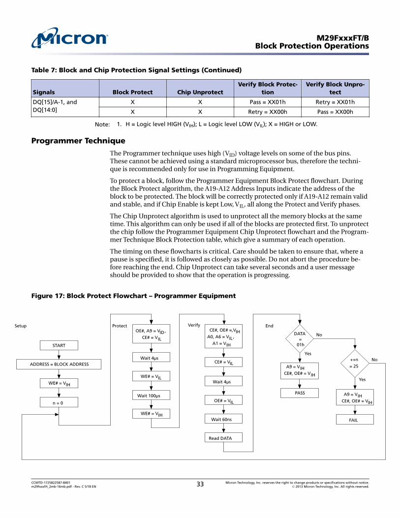
Table 7: Block and Chip Protection Signal Settings (Continued)
Signals Block Protect Chip UnprotectVerify Block Protec-
tionVerify Block Unpro-
tect
DQ[15]/A-1, andDQ[14:0]
X X Pass = XX01h Retry = XX01h
X X Retry = XX00h Pass = XX00h
Note: 1. H = Logic level HIGH (VIH); L = Logic level LOW (VIL); X = HIGH or LOW.
Programmer Technique
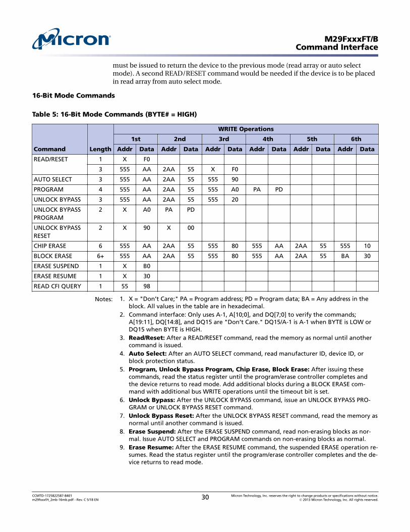
The Programmer technique uses high (VID) voltage levels on some of the bus pins.These cannot be achieved using a standard microprocessor bus, therefore the techni-que is recommended only for use in Programming Equipment.
To protect a block, follow the Programmer Equipment Block Protect flowchart. Duringthe Block Protect algorithm, the A19-A12 Address Inputs indicate the address of theblock to be protected. The block will be correctly protected only if A19-A12 remain validand stable, and if Chip Enable is kept Low, VIL, all along the Protect and Verify phases.
The Chip Unprotect algorithm is used to unprotect all the memory blocks at the sametime. This algorithm can only be used if all of the blocks are protected first. To unprotectthe chip follow the Programmer Equipment Chip Unprotect flowchart and the Program-mer Technique Block Protection table, which give a summary of each operation.
The timing on these flowcharts is critical. Care should be taken to ensure that, where apause is specified, it is followed as closely as possible. Do not abort the procedure be-fore reaching the end. Chip Unprotect can take several seconds and a user messageshould be provided to show that the operation is progressing.
Figure 17: Block Protect Flowchart – Programmer Equipment
VerifyProtectSetup End
ADDRESS = BLOCK ADDRESS
n = 0
START
WE# = VIH
OE#, A9 = VID ,
CE# = VIL
Wait 4µs
Wait 100µs
WE# = VIL
WE# = VIH
CE#, OE# = VIH,
A0, A6 = VIL ,
A1 = VIH
DATA=
01h
Yes
Yes
No
CE# = VIL
Wait 4µs
OE# = VIL
Wait 60ns
Read DATA
A9 = VIHCE#, OE# = VIH
++n
= 25
FAIL
PASS A9 = VIHCE#, OE# = VIH
No
M29FxxxFT/BBlock Protection Operations
CCMTD-1725822587-8401m29fxxxf/t_2mb-16mb.pdf - Rev. C 5/18 EN 33 Micron Technology, Inc. reserves the right to change products or specifications without notice.
© 2013 Micron Technology, Inc. All rights reserved.

Figure 18: Chip Unprotect Flowchart – Programmer Equipment
PROTECT ALL BLOCKS
A6, A12, A15 = V IHCE#, OE#, A9 = V ID
DATA
WE# = VIH
CE#, OE# = VIH
ADDRESS = CURRENT BLOCK ADDRESS
A0 = VIL , A1, A6 = VIH
Wait 10ms
=00h
INCREMENT
CURRENT BLOCK
n = 0
CURRENT BLOCK = 0
Wait 4µs
WE# = VIL
++n
= 1000
START
YES
YESNO
NO LAST
BLOCK
YES
NO
CE# = VIL
Wait 4µs
OE# = VIL
Wait 60ns
Read DATA
FAIL PASS
Ver
ify
Un
pro
tect
Set-
up
End
A9 = VIHCE#, OE# = VIH
A9 = VIHCE#, OE# = VIH
M29FxxxFT/BBlock Protection Operations
CCMTD-1725822587-8401m29fxxxf/t_2mb-16mb.pdf - Rev. C 5/18 EN 34 Micron Technology, Inc. reserves the right to change products or specifications without notice.
© 2013 Micron Technology, Inc. All rights reserved.
Notes: 1. Address Inputs A[9:12] give the address of the block that is to be protected. It is impera-tive that they remain stable during the operation.
2. During the protect and verify phases of the algorithm, CE# must be kept LOW.
In-System Technique
The In-System technique requires a high voltage level on the Reset/Blocks TemporaryUnprotect pin, RP. This can be achieved without violating the maximum ratings of thecomponents on the microprocessor bus, therefore this technique is suitable for use af-ter the Flash memory has been fitted to the system.
To protect a block follow the In-System Equipment Block Protect flowchart . To unpro-tect the whole chip it is necessary to protect all of the blocks first, then all the blocks canbe unprotected at the same time. To unprotect the chip follow the In-System Equip-ment Chip Unprotect flowchart.
The timing on these flowcharts is critical. Care should be taken to ensure that, where apause is specified, it is followed as closely as possible. Do not allow the microprocessorto service interrupts that will upset the timing and do not abort the procedure beforereaching the end. Chip Unprotect can take several seconds and a user message shouldbe provided to show that the operation is progressing.
Figure 19: Block Protect Flowchart – In-System Equipment
No
IH
WRITE 60h
ADDRESS = BLOCK ADDRESS
A0 = VIL , A1 = VIH , A6 = VIL
Wait 100µs
WRITE 40h
ADDRESS = BLOCK ADDRESS
A0 = VIL , A1 = VIH , A6 = VIL
Wait 4µs
READ DATA
ADDRESS = BLOCK ADDRESS
A0 = VIL , A1 = VIH , A6 = VIL
Verify
Protect
n = 0
START
RST# = VID
WRITE 60h
ADDRESS = BLOCK ADDRESS
A0 = VIL , A1 = VIH , A6 = VIL
Setup
RST# = VIH
++n
= 25
FAIL
PASS
Yes
DATA=
01h
Yes
No
RST# = V
ISSUE READ/RESET
COMMAND
ISSUE READ/RESET
COMMAND
End
M29FxxxFT/BBlock Protection Operations
CCMTD-1725822587-8401m29fxxxf/t_2mb-16mb.pdf - Rev. C 5/18 EN 35 Micron Technology, Inc. reserves the right to change products or specifications without notice.
© 2013 Micron Technology, Inc. All rights reserved.
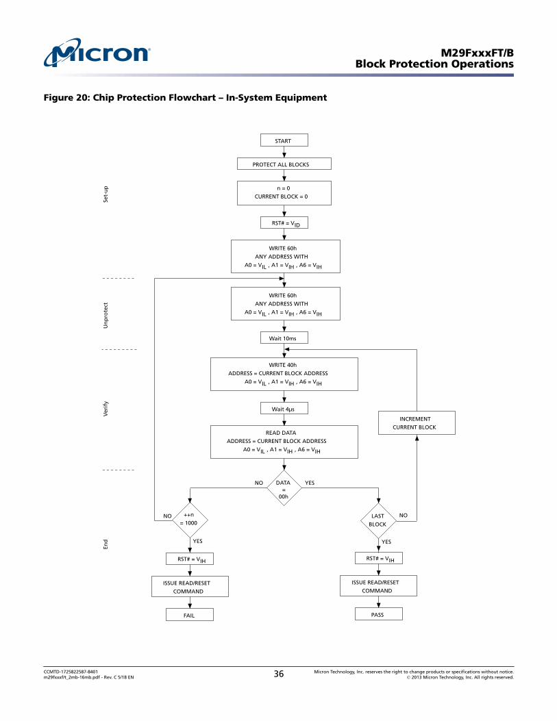
Figure 20: Chip Protection Flowchart – In-System Equipment
WRITE 60h
ANY ADDRESS WITH
A0 = VIL , A1 = VIH , A6 = VIH
n = 0
CURRENT BLOCK = 0
Wait 10ms
WRITE 40h
ADDRESS = CURRENT BLOCK ADDRESS
A0 = VIL , A1 = VIH , A6 = VIH
RST# = VIH
++n
= 1000
START
FAIL PASS
YES
NO
DATA=
00h
YESNO
RST# = VIH
Wait 4µs
READ DATA
ADDRESS = CURRENT BLOCK ADDRESS
A0 = VIL , A1 = VIH , A6 = VIH
RST# = VID
ISSUE READ/RESET
COMMANDISSUE READ/RESET
COMMAND
PROTECT ALL BLOCKS
INCREMENT
CURRENT BLOCK
LAST
BLOCK
YES
NO
WRITE 60h
ANY ADDRESS WITH
A0 = VIL , A1 = VIH , A6 = VIH
Ver
ify
Un
pro
tect
Set-
up
End
M29FxxxFT/BBlock Protection Operations
CCMTD-1725822587-8401m29fxxxf/t_2mb-16mb.pdf - Rev. C 5/18 EN 36 Micron Technology, Inc. reserves the right to change products or specifications without notice.
© 2013 Micron Technology, Inc. All rights reserved.

Status RegisterBus Read operations from any address always read the Status Register during Programand Erase operations. It is also read during Erase Suspend when an address within ablock being erased is accessed.
Table 8: Status Register Bits
Operation Address DQ7 DQ6 DQ5 DQ3 DQ2 RB#
Program Any Address DQ7# Toggle 0 – – 0
Program During EraseSuspend
Any Address DQ7# Toggle 0 – – 0
Program Error Any Address DQ7# Toggle 1 – – 0
Chip Erase Any Address 0 Toggle 0 1 Toggle 0
Block Erase before time-out
Erasing Block 0 Toggle 0 0 Toggle 0
Non-Erasing Block 0 Toggle 0 0 No Toggle 0
Block Erase Erasing Block 0 Toggle 0 1 Toggle 0
Non-Erasing Block 0 Toggle 0 1 No Toggle 0
Erase Suspend Erasing Block 1 No Toggle 0 – Toggle 1
Non-Erasing Block Data read as normal 1
Erase Error Good Block Ad-dress
0 Toggle 1 1 No Toggle 0
Faulty Block Ad-dress
0 Toggle 1 1 Toggle 0
Note: 1. Unspecified data bits should be ignored.
Data Polling Bit
The Data Polling Bit (DQ7) can be used to identify whether the Program/Erase Control-ler has successfully completed its operation or if it has responded to an Erase Suspend.The Data Polling Bit is output on DQ7 when the Status Register is read.
During Program operations the Data Polling Bit outputs the complement of the bit be-ing programmed to DQ7. After successful completion of the Program operation thememory returns to Read mode and Bus Read operations from the address just program-med output DQ7, not its complement.
During Erase operations the Data Polling Bit outputs ’0’, the complement of the erasedstate of DQ7. After successful completion of the Erase operation the memory returns toRead Mode.
In Erase Suspend mode the Data Polling Bit will output a ’1’ during a Bus Read opera-tion within a block being erased. The Data Polling Bit will change from a ’0’ to a ’1’when the Program/Erase Controller has suspended the Erase operation.
The Data Polling Flowchart, gives an example of how to use the Data Polling Bit. A ValidAddress is the address being programmed or an address within the block being erased.
M29FxxxFT/BStatus Register
CCMTD-1725822587-8401m29fxxxf/t_2mb-16mb.pdf - Rev. C 5/18 EN 37 Micron Technology, Inc. reserves the right to change products or specifications without notice.
© 2013 Micron Technology, Inc. All rights reserved.

Figure 21: Data Polling Flowchart
Read DQ5 and DQ7at valid address
Start
Read DQ7at valid address
Fail Pass AI03598
DQ7= data
Yes
No
Yes
No
DQ5= 1
DQ7= data
Yes
No
Toggle Bit
The Toggle Bit (DQ6) can be used to identify whether the Program/Erase Controller hassuccessfully completed its operation or if it has responded to an Erase Suspend. TheToggle Bit is output on DQ6 when the Status Register is read.
During Program and Erase operations the Toggle Bit changes from ’0’ to ’1’ to ’0’, etc.,with successive Bus Read operations at any address. After successful completion of theoperation the memory returns to Read mode.
During Erase Suspend mode the Toggle Bit will output when addressing a cell within ablock being erased. The Toggle Bit will stop toggling when the Program/Erase Controllerhas suspended the Erase operation.
If any attempt is made to erase a protected block, the operation is aborted, no error issignalled and DQ6 toggles for approximately 100µs. If any attempt is made to program aprotected block or a suspended block, the operation is aborted, no error is signalled andDQ6 toggles for approximately 1µs.
The Data Toggle Flowchart, gives an example of how to use the Data Toggle Bit.
M29FxxxFT/BStatus Register
CCMTD-1725822587-8401m29fxxxf/t_2mb-16mb.pdf - Rev. C 5/18 EN 38 Micron Technology, Inc. reserves the right to change products or specifications without notice.
© 2013 Micron Technology, Inc. All rights reserved.

Figure 22: Data Toggle Flowchart
Read DQ6
Start
Read DQ6twice
Fail Pass
AI01370C
DQ6= toggle
No
No
Yes
Yes
DQ5 = 1
No
Yes
DQ6= toggle
ReadDQ5 and DQ6
Error Bit
The Error Bit (DQ5) can be used to identify errors detected by the Program/Erase Con-troller. The Error Bit is set to ’1’ when a Program, Block Erase or Chip Erase operationfails to write the correct data to the memory. If the Error Bit is set a Read/Reset com-mand must be issued before other commands are issued. The Error bit is output onDQ5 when the Status Register is read.
Note that the Program command cannot change a bit set to ’0’ back to ’1’ and attempt-ing to do so will set DQ5 to ‘1’. A Bus Read operation to that address will show the bit isstill ‘0’. One of the Erase commands must be used to set all the bits in a block or in thewhole memory from ’0’ to ’1’
Erase Timer Bit
The Erase Timer Bit (DQ3) can be used to identify the start of Program/Erase Controlleroperation during a Block Erase command. Once the Program/Erase Controller startserasing the Erase Timer Bit is set to ’1’. Before the Program/Erase Controller starts theErase Timer Bit is set to ’0’ and additional blocks to be erased may be written to theCommand Interface. The Erase Timer Bit is output on DQ3 when the Status Register isread.
M29FxxxFT/BStatus Register
CCMTD-1725822587-8401m29fxxxf/t_2mb-16mb.pdf - Rev. C 5/18 EN 39 Micron Technology, Inc. reserves the right to change products or specifications without notice.
© 2013 Micron Technology, Inc. All rights reserved.
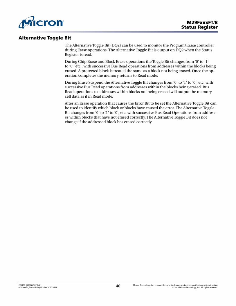
Alternative Toggle Bit
The Alternative Toggle Bit (DQ2) can be used to monitor the Program/Erase controllerduring Erase operations. The Alternative Toggle Bit is output on DQ2 when the StatusRegister is read.
During Chip Erase and Block Erase operations the Toggle Bit changes from ’0’ to ’1’to ’0’, etc., with successive Bus Read operations from addresses within the blocks beingerased. A protected block is treated the same as a block not being erased. Once the op-eration completes the memory returns to Read mode.
During Erase Suspend the Alternative Toggle Bit changes from ’0’ to ’1’ to ’0’, etc. withsuccessive Bus Read operations from addresses within the blocks being erased. BusRead operations to addresses within blocks not being erased will output the memorycell data as if in Read mode.
After an Erase operation that causes the Error Bit to be set the Alternative Toggle Bit canbe used to identify which block or blocks have caused the error. The Alternative ToggleBit changes from ’0’ to ’1’ to ’0’, etc. with successive Bus Read Operations from address-es within blocks that have not erased correctly. The Alternative Toggle Bit does notchange if the addressed block has erased correctly.
M29FxxxFT/BStatus Register
CCMTD-1725822587-8401m29fxxxf/t_2mb-16mb.pdf - Rev. C 5/18 EN 40 Micron Technology, Inc. reserves the right to change products or specifications without notice.
© 2013 Micron Technology, Inc. All rights reserved.

Common Flash Interface (CFI)The Common Flash Interface is a JEDEC approved, standardized data structure that canbe read from the Flash memory device. It allows a system software to query the deviceto determine various electrical and timing parameters, density information and func-tions supported by the memory. The system can interface easily with the device, ena-bling the software to upgrade itself when necessary.
When the CFI Query Command is issued the device enters CFI Query mode and the da-ta structure is read from the memory. Addresses used to retrieve the data are shown inthe following tables:
The CFI data structure also contains a security area where a 64-bit unique securitynumber is written. This area can be accessed only in Read mode by the final user. It isimpossible to change the security number after it has been written by Micron. Issue aRead command to return to Read mode.
Table 9: Query Structure Overview
Address
Sub-section Name Descriptionx16 x8
10h 20h CFI Query Identification String Command set ID and algorithm data offset
1Bh 36h System Interface Information Device timing & voltage information
27h 4Eh Device Geometry Definition Flash device layout
40h 80h Primary Algorithm-specific Extended Querytable
Additional information specific to the Pri-mary Algorithm (optional)
61h C2h Security Code Area 64 bit unique device number
Note: 1. Query data are always presented on the lowest order data outputs.
Table 10: CFI Query Identification String
Address
Data Description Valuex16 x8
10h 20h 0051h "Q"
11h 22h 0052h Query Unique ASCII String "QRY" "R"
12h 24h 0059h "Y"
13h 26h 0002h Primary Algorithm Command Set and Control Interface IDcode 16 bit ID code defining a specific algorithm
AMDCompatible14h 28h 0000h
15h 2Ah 0040h Address for Primary Algorithm extended Query table (seethe Device Geometry table.)
P = 40h
16h 2Ch 0000h
17h 2Eh 0000h Alternate Vendor Command Set and Control Interface IDCode second vendor - specified algorithm supported
NA
18h 30h 0000h
19h 32h 0000h Address for Alternate Algorithm extended Query table NA
1Ah 34h 0000h
Note: 1. Query data are always presented on the lowest order data outputs (DQ7-DQ0) only.DQ8-DQ15 are ‘0’.
M29FxxxFT/BCommon Flash Interface (CFI)
CCMTD-1725822587-8401m29fxxxf/t_2mb-16mb.pdf - Rev. C 5/18 EN 41 Micron Technology, Inc. reserves the right to change products or specifications without notice.
© 2013 Micron Technology, Inc. All rights reserved.

Table 11: CFI Query System Interface Information
Address
Data Description Valuex16 x8
1Bh 36h 0045h VCC Logic Supply Minimum Program/Erase voltagebit 7 to 4 BCD value in voltsbit 3 to 0 BCD value in 100 mV
4.5V
1Ch 38h 0055h VCC Logic Supply Maximum Program/Erase voltagebit 7 to 4 BCD value in voltsbit 3 to 0 BCD value in 100 mV
5.5V
1Dh 3Ah 0000h VPP [Programming] Supply Minimum Program/Erase voltage NA
1Eh 3Ch 0000h VPP [Programming] Supply Maximum Program/Erase voltage NA
1Fh 3Eh 0003h Typical timeout per single Byte/Word program = 2n µs 8µs
20h 40h 0000h Typical timeout for minimum size write buffer program = 2n µs NA
21h 42h 000Ah Typical timeout per individual block erase = 2n ms 1 s
22h 44h 0000h Typical timeout for full chip erase = 2n ms NA
23h 46h 0004h Maximum timeout for Byte/Word program = 2n times typical 256µs
24h 48h 0000h Maximum timeout for write buffer program = 2n times typical NA
25h 4Ah 0003h Maximum timeout per individual block erase = 2n times typical 8 s
26h 4Ch 0000h Maximum timeout for chip erase = 2n times typical NA
Table 12: Device Geometry Definition
Address
Data Description Valuex16 x8
27h 4Eh 0015h Device Size = 2n in number of Bytes 2MB
0014h 1MB
0013h 512KB
0012h 256KB
28h29h
50h52h
0002h0000h
Flash Device Interface Code description x8, x16Async.
2Ah2Bh
54h56h
0000h0000h
Maximum number of Bytes in multi-Byte program or page = 2n NA
2Ch 58h 0004h Number of Erase Block Regions within the device.It specifies the number of regions within the device containingcontiguous Erase Blocks of the same size.
4
2Dh2Eh
5Ah5Ch
0000h0000h
Region 1 InformationNumber of identical size erase block = 0000h+1
1
2Fh30h
5Eh60h
0040h0000h
Region 1 InformationBlock size in Region 1 = 0040h * 256 Byte
16KB
31h32h
62h64h
0001h0000h
Region 2 InformationNumber of identical size erase block = 0001h+1
2
33h34h
66h68h
0020h0000h
Region 2 InformationBlock size in Region 2 = 0020h * 256 Byte
8KB
M29FxxxFT/BCommon Flash Interface (CFI)
CCMTD-1725822587-8401m29fxxxf/t_2mb-16mb.pdf - Rev. C 5/18 EN 42 Micron Technology, Inc. reserves the right to change products or specifications without notice.
© 2013 Micron Technology, Inc. All rights reserved.
Table 12: Device Geometry Definition (Continued)
Address
Data Description Valuex16 x8
35h36h
6Ah6Ch
0000h0000h
Region 3 InformationNumber of identical size erase block = 0000h+1
1
37h38h
6Eh70h
0080h0000h
Region 3 InformationBlock size in Region 3 = 0080h * 256 Byte
32KB
39h3Ah
72h74h
001Eh0000h
Region 4 Information (2 MByte)Number of identical-size erase block = 001Eh+1
31
39h3Ah
72h74h
000Eh0000h
Region 4 Information (1 MByte)Number of identical-size erase block = 000Eh+1
15
39h3Ah
72h74h
0006h0000h
Region 4 Information (512 KByte)Number of identical-size erase block = 0006h+1
7
39h3Ah
72h74h
0002h0000h
Region 4 Information (256 KByte)Number of identical-size erase block = 0002h+1
3
3Bh3Ch
76h78h
0000h0001h
Region 4 InformationBlock size in Region 4 = 0100h * 256 Byte
64KB
Table 13: Primary Algorithm-Specific Extended Query Table
Address
Data Description Valuex16 x8
40h 80h 0050h Primary Algorithm extended Query table unique ASCII string “PRI” "P"
41h 82h 0052h "R"
42h 84h 0049h "I"
43h 86h 0031h Major version number, ASCII "1"
44h 88h 0030h Minor version number, ASCII "0"
45h 8Ah 0000h Address Sensitive Unlock (bits 1 to 0)00 = required, 01= not requiredSilicon Revision Number (bits 7 to 2)
Yes
46h 8Ch 0002h Erase Suspend00 = not supported, 01 = Read only, 02 = Read and Write
2
47h 8Eh 0001h Block Protection00 = not supported, x = number of blocks in per group
1
48h 90h 0001h Temporary Block Unprotect00 = not supported, 01 = supported
Yes
49h 92h 0002h0004h
0008h
0160h
Block Protect /Unprotect02 = M29F20004 = M29F40008 = M29F80010 = M29F160
248
16
4Ah 94h 0000h Simultaneous Operations, 00 = not supported No
4Bh 96h 0000h Burst Mode, 00 = not supported, 01 = supported No
M29FxxxFT/BCommon Flash Interface (CFI)
CCMTD-1725822587-8401m29fxxxf/t_2mb-16mb.pdf - Rev. C 5/18 EN 43 Micron Technology, Inc. reserves the right to change products or specifications without notice.
© 2013 Micron Technology, Inc. All rights reserved.

Table 13: Primary Algorithm-Specific Extended Query Table (Continued)
Address
Data Description Valuex16 x8
4Ch 98h 0000h Page Mode, 00 = not supported, 01 = 4 page Word, 02 = 8 page Word No
Table 14: Security Code Area
Address
Data Descriptionx16 x8
61h C3h, C2h XXXX 64 bit: unique device number
62h C5h, C4h XXXX
63h C7h, C6h XXXX
64h C9h, C8h XXXX
M29FxxxFT/BCommon Flash Interface (CFI)
CCMTD-1725822587-8401m29fxxxf/t_2mb-16mb.pdf - Rev. C 5/18 EN 44 Micron Technology, Inc. reserves the right to change products or specifications without notice.
© 2013 Micron Technology, Inc. All rights reserved.

Maximum Ratings and Operating ConditionsStressing the device above the rating listed in the Absolute Maximum Ratings table maycause permanent damage to the device. Exposure to Absolute Maximum Rating condi-tions for extended periods may affect device reliability. These are stress ratings only andoperation of the device at these or any other conditions above those indicated in theOperating sections of this specification is not implied.
Table 15: Absolute Maximum Ratings
Symbol Parameter Min Max Unit
TBIAS Temperature Under Bias –50 125 °C
TSTG Storage Temperature –65 150 °C
VIO Input or Output Voltage –0.6 VCC +0.6 V
VCC Supply Voltage –0.6 6 V
VID Identification Voltage –0.6 13.5 V
Notes: 1. Input or Output Voltage parameter: Minimum voltage may undershoot to –2V duringtransition and for less than 20ns during transitions.
2. Input or Output Voltage parameter: Maximum voltage may overshoot to VCC +2V duringtransition and for less than 20ns during transitions.
The parameters in the tables that follow, are derived from tests performed under theMeasurement Conditions shown here. Designers should check that the operating con-ditions in their circuit match the operating conditions when relying on the quoted pa-rameters.
Table 16: Operating and AC Measurement Conditions
Parameter Min Max Unit
VCC Supply Voltage 4.5 5.5 V
Ambient Operating Temperature –40 125 °C
Load Capacitance (CL) 30 30 pF
Input Rise and Fall Times — 5 ns
Input Pulse Voltages 0 to VCC 0 to VCC V
Input and Output Timing Reference Voltages VCC/2 VCC/2 V
Figure 23: AC Measurement I/O Waveform
AI04498
VCC
0V
VCC/2
M29FxxxFT/BMaximum Ratings and Operating Conditions
CCMTD-1725822587-8401m29fxxxf/t_2mb-16mb.pdf - Rev. C 5/18 EN 45 Micron Technology, Inc. reserves the right to change products or specifications without notice.
© 2013 Micron Technology, Inc. All rights reserved.

Figure 24: AC Measurement Load Circuit
CL
CL includes JIG capacitance
25k W
VCC
25k W
VCC
0.1 µF
Device under test
Table 17: Device Capacitance
Symbol Parameter Test Condition Min Max Unit
CIN Input Capacitance VIN = 0V 6 pF
COUT Output Capacitance VOUT = 0V 12 pF
Note: 1. Sampled only, not 100% tested.
M29FxxxFT/BMaximum Ratings and Operating Conditions
CCMTD-1725822587-8401m29fxxxf/t_2mb-16mb.pdf - Rev. C 5/18 EN 46 Micron Technology, Inc. reserves the right to change products or specifications without notice.
© 2013 Micron Technology, Inc. All rights reserved.
DC Electrical Specifications
Table 18: DC Characteristics
Symbol Parameter Test Condition Min Typ Max Unit
ILI Input Leakage Current 0V ≤ VIN ≤ VCC — — ±1 µA
ILO Output Leakage Current 0V ≤ VOUT ≤ VCC — — ±1 µA
ICC1 Supply Current (Read) CE# = VIL, OE# = VIH,f = 6MHz
— 7 20 mA
ICC2 Supply Current (Standby) CE# = VCC ±0.2V,RP# = VCC ±0.2V
— 60 120 µA
ICC3 Supply Current (Program/Erase) Program/Erase Controller active — — 30 mA
VIL Input Low Voltage – –0.5 — 0.8 V
VIH Input High Voltage – 0.7VCC — VCC +0.3 V
VOL Output Low Voltage IOL = 1.8mA — — 0.45 V
VOH Output High Voltage IOH = –100µA VCC –0.4 — — V
VID Identification Voltage 11.5 — 12.5 V
IID Identification Current A9 = VID — — 100 µA
VLKO Program/Erase Lockout SupplyVoltage
– 1.8 — 2.3 V
Note: 1. Supply Current (Program/Erase) parameter: Sampled only, not 100% tested.
M29FxxxFT/BDC Electrical Specifications
CCMTD-1725822587-8401m29fxxxf/t_2mb-16mb.pdf - Rev. C 5/18 EN 47 Micron Technology, Inc. reserves the right to change products or specifications without notice.
© 2013 Micron Technology, Inc. All rights reserved.
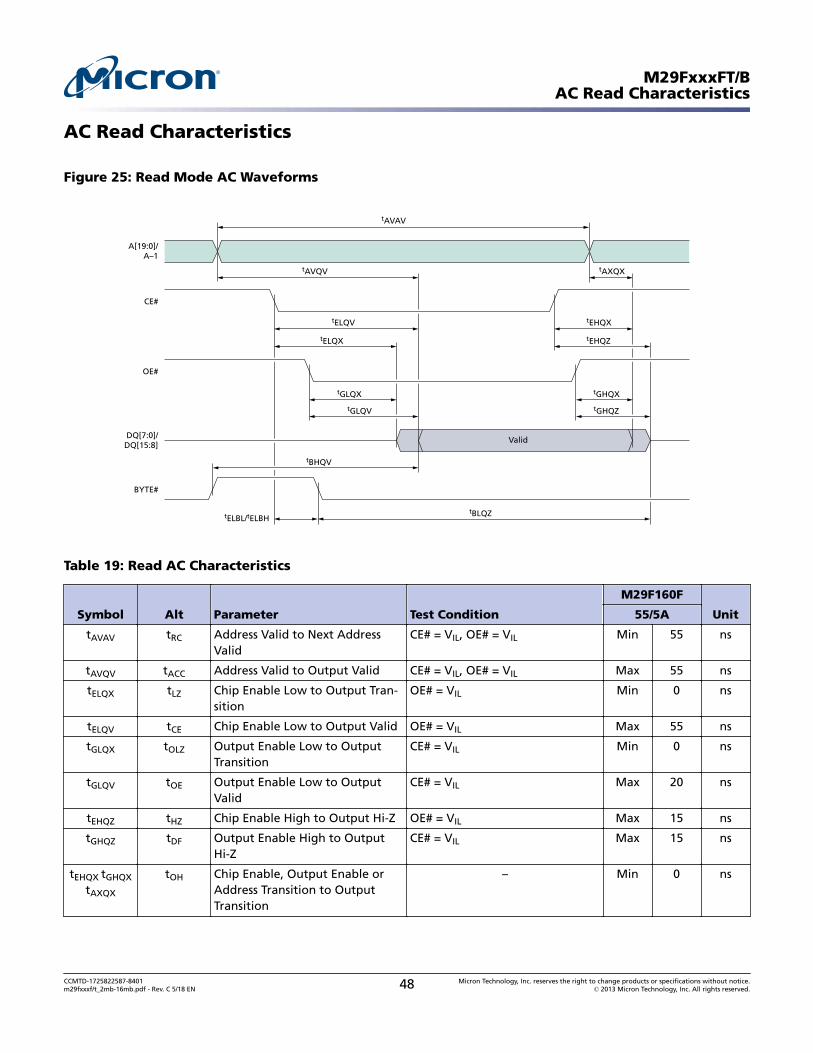
AC Read Characteristics
Figure 25: Read Mode AC Waveforms
tAVAV
tAVQV tAXQX
tELQX tEHQZ
tGLQV
tGLQX tGHQX
Valid
A[19:0]/A–1
OE#
DQ[7:0]/DQ[15:8]
CE#
tELQV tEHQX
tGHQZ
Valid
tBHQV
tELBL/tELBHtBLQZ
BYTE#
Table 19: Read AC Characteristics
Symbol Alt Parameter Test Condition
M29F160F
Unit55/5A
tAVAV tRC Address Valid to Next AddressValid
CE# = VIL, OE# = VIL Min 55 ns
tAVQV tACC Address Valid to Output Valid CE# = VIL, OE# = VIL Max 55 ns
tELQX tLZ Chip Enable Low to Output Tran-sition
OE# = VIL Min 0 ns
tELQV tCE Chip Enable Low to Output Valid OE# = VIL Max 55 ns
tGLQX tOLZ Output Enable Low to OutputTransition
CE# = VIL Min 0 ns
tGLQV tOE Output Enable Low to OutputValid
CE# = VIL Max 20 ns
tEHQZ tHZ Chip Enable High to Output Hi-Z OE# = VIL Max 15 ns
tGHQZ tDF Output Enable High to OutputHi-Z
CE# = VIL Max 15 ns
tEHQX tGHQX
tAXQX
tOH Chip Enable, Output Enable orAddress Transition to OutputTransition
– Min 0 ns
M29FxxxFT/BAC Read Characteristics
CCMTD-1725822587-8401m29fxxxf/t_2mb-16mb.pdf - Rev. C 5/18 EN 48 Micron Technology, Inc. reserves the right to change products or specifications without notice.
© 2013 Micron Technology, Inc. All rights reserved.

Table 19: Read AC Characteristics (Continued)
Symbol Alt Parameter Test Condition
M29F160F
Unit55/5A
tELBL
tELBH
tELFL tELFH Chip Enable to BYTE# Low orHigh
– Max 3 ns
tBLQZ tFLQZ BYTE# Low to Output Hi-Z – Max 15 ns
tBHQV tFHQV BYTE# High to Output Valid – Max 20 ns
Note: 1. tELQX tGLQX tEHQZ and tGHQZ parameters: Sampled only, not 100% tested.
M29FxxxFT/BAC Read Characteristics
CCMTD-1725822587-8401m29fxxxf/t_2mb-16mb.pdf - Rev. C 5/18 EN 49 Micron Technology, Inc. reserves the right to change products or specifications without notice.
© 2013 Micron Technology, Inc. All rights reserved.

AC Write Characteristics
Figure 26: Write AC Waveforms, Write Enable Controlled
CE#
OE#
WE#
A[19:0]/A–1
DQ[7:0]/DQ[15:8]
VCC
R/B#
Valid
Valid
tVCHEL
tWHEH
tWHWL
tELWL
tAVWL
tWHGL
tWLAX
tWHDX
tAVAV
tDVWH
tWLWHtGHWL
tWHRL
Table 20: Write AC Characteristics, Write Enable Controlled
Symbol Alternate Parameter
M29F160F
Unit55/5A
tAVAV tWC Address Valid to Next Address Valid Min 55 ns
tELWL tCS Chip Enable Low to Write Enable Low Min 0 ns
tWLWH tWP Write Enable Low to Write Enable High Min 30 ns
tDVWH tDS Input Valid to Write Enable High Min 20 ns
tWHDX tDH Write Enable High to Input Transition Min 0 ns
tWHEH tCH Write Enable High to Chip Enable High Min 0 ns
tWHWL tWPH Write Enable High to Write Enable Low Min 15 ns
tAVWL tAS Address Valid to Write Enable Low Min 0 ns
tWLAX tAH Write Enable Low to Address Transition Min 30 ns
tGHWL Output Enable High to Write Enable Low Min 0 ns
tWHGL tOEH Write Enable High to Output Enable Low Min 0 ns
tWHRL tBUSY Program/Erase Valid to RB# Low Max 20 ns
M29FxxxFT/BAC Write Characteristics
CCMTD-1725822587-8401m29fxxxf/t_2mb-16mb.pdf - Rev. C 5/18 EN 50 Micron Technology, Inc. reserves the right to change products or specifications without notice.
© 2013 Micron Technology, Inc. All rights reserved.
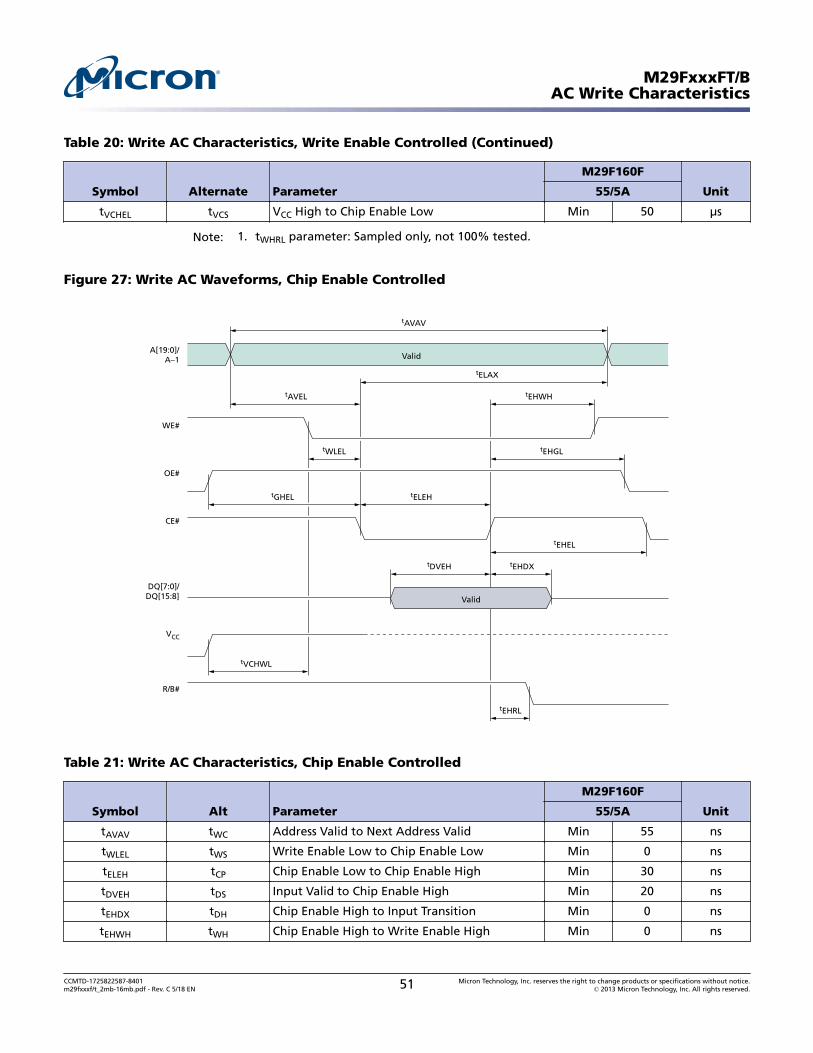
Table 20: Write AC Characteristics, Write Enable Controlled (Continued)
Symbol Alternate Parameter
M29F160F
Unit55/5A
tVCHEL tVCS VCC High to Chip Enable Low Min 50 µs
Note: 1. tWHRL parameter: Sampled only, not 100% tested.
Figure 27: Write AC Waveforms, Chip Enable Controlled
Valid
Valid
tVCHWL
tEHWH
tEHEL
tWLEL
tAVEL
tEHGL
tELAX
tEHDX
tAVAV
tDVEH
tELEHtGHEL
tEHRL
CE#
OE#
WE#
A[19:0]/A–1
DQ[7:0]/DQ[15:8]
VCC
R/B#
Table 21: Write AC Characteristics, Chip Enable Controlled
Symbol Alt Parameter
M29F160F
Unit55/5A
tAVAV tWC Address Valid to Next Address Valid Min 55 ns
tWLEL tWS Write Enable Low to Chip Enable Low Min 0 ns
tELEH tCP Chip Enable Low to Chip Enable High Min 30 ns
tDVEH tDS Input Valid to Chip Enable High Min 20 ns
tEHDX tDH Chip Enable High to Input Transition Min 0 ns
tEHWH tWH Chip Enable High to Write Enable High Min 0 ns
M29FxxxFT/BAC Write Characteristics
CCMTD-1725822587-8401m29fxxxf/t_2mb-16mb.pdf - Rev. C 5/18 EN 51 Micron Technology, Inc. reserves the right to change products or specifications without notice.
© 2013 Micron Technology, Inc. All rights reserved.
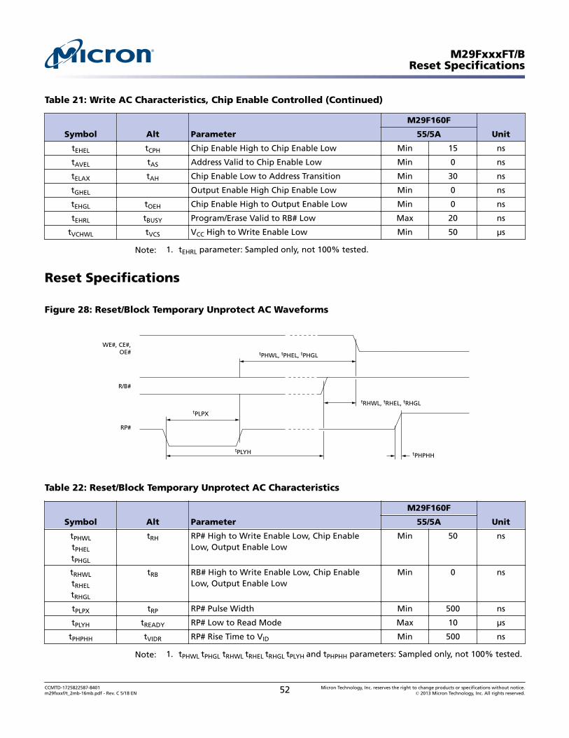
Table 21: Write AC Characteristics, Chip Enable Controlled (Continued)
Symbol Alt Parameter
M29F160F
Unit55/5A
tEHEL tCPH Chip Enable High to Chip Enable Low Min 15 ns
tAVEL tAS Address Valid to Chip Enable Low Min 0 ns
tELAX tAH Chip Enable Low to Address Transition Min 30 ns
tGHEL Output Enable High Chip Enable Low Min 0 ns
tEHGL tOEH Chip Enable High to Output Enable Low Min 0 ns
tEHRL tBUSY Program/Erase Valid to RB# Low Max 20 ns
tVCHWL tVCS VCC High to Write Enable Low Min 50 µs
Note: 1. tEHRL parameter: Sampled only, not 100% tested.
Reset Specifications
Figure 28: Reset/Block Temporary Unprotect AC Waveforms
R/B#
WE#, CE#,OE#
RP#
tPLPX
tPHWL, tPHEL, tPHGL
tPLYH tPHPHH
tRHWL, tRHEL, tRHGL
Table 22: Reset/Block Temporary Unprotect AC Characteristics
Symbol Alt Parameter
M29F160F
Unit55/5A
tPHWL
tPHEL
tPHGL
tRH RP# High to Write Enable Low, Chip EnableLow, Output Enable Low
Min 50 ns
tRHWL
tRHEL
tRHGL
tRB RB# High to Write Enable Low, Chip EnableLow, Output Enable Low
Min 0 ns
tPLPX tRP RP# Pulse Width Min 500 ns
tPLYH tREADY RP# Low to Read Mode Max 10 µs
tPHPHH tVIDR RP# Rise Time to VID Min 500 ns
Note: 1. tPHWL tPHGL tRHWL tRHEL tRHGL tPLYH and tPHPHH parameters: Sampled only, not 100% tested.
M29FxxxFT/BReset Specifications
CCMTD-1725822587-8401m29fxxxf/t_2mb-16mb.pdf - Rev. C 5/18 EN 52 Micron Technology, Inc. reserves the right to change products or specifications without notice.
© 2013 Micron Technology, Inc. All rights reserved.

PROGRAM/ERASE Characteristics
Table 23: Program/Erase Characteristics
Parameter Min Typ Max Unit
Chip erase M29F160F — 25 120 s
M29F800F 12 60
M29F400F 6 30
M29F200F 3 15
Block erase (64KB) — 0.8 6 s
Erase suspend latency time — 20 25 µs
Program (byte or word) — 11 200 µs
Chip program (byte-by-byte) M29F160F — 24 120 s
M29F800F 12 60
M29F400F 6 30
M29F200F 4 16
Chip program (word-by-word) M29F160F — 12 60 s
M29F800F 6 30
M29F400F 3 15
M29F200F 2 8
PROGRAM/ERASE cycles (per block) 100,000 — — cycles
Data retention 20 — — years
Notes: 1. Typical values are measured at room temperature and nominal voltages; typical andmaximum values are samples, not 100% tested.
2. Chip erase, program, and chip program parameters: Maximum value measured at worstcase conditions for both temperature and VCC after 100,000 PROGRAM/ERASE cycles.
3. Block erase and erase suspend latency parameter: Maximum value measured at worst-case conditions for both temperature and VCC.
M29FxxxFT/BPROGRAM/ERASE Characteristics
CCMTD-1725822587-8401m29fxxxf/t_2mb-16mb.pdf - Rev. C 5/18 EN 53 Micron Technology, Inc. reserves the right to change products or specifications without notice.
© 2013 Micron Technology, Inc. All rights reserved.

Package Dimensions
Figure 29: 48-Lead TSOP – 12mm x 20mm
Die
1
24
48
25
0.50 TYP
0.08 MAX
0.10 MIN/0.21 MAX 0.60 +0.10
+3o 2o
3o
0.22 +0.05
0.10 +0.05
1.20 MAX1.00 +0.05
0.80 TYP
20.00 +0.20
18.40 +0.10
12.00 +0.10
Note: 1. Drawing is not to scale.
M29FxxxFT/BPackage Dimensions
CCMTD-1725822587-8401m29fxxxf/t_2mb-16mb.pdf - Rev. C 5/18 EN 54 Micron Technology, Inc. reserves the right to change products or specifications without notice.
© 2013 Micron Technology, Inc. All rights reserved.
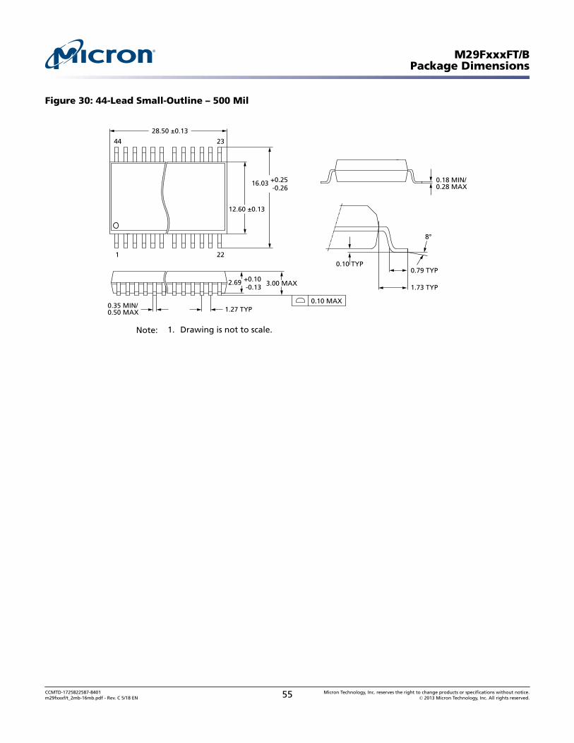
Figure 30: 44-Lead Small-Outline – 500 Mil
44
1 22
23
8°
0.35 MIN/0.50 MAX
0.18 MIN/0.28 MAX
0.10 TYP0.79 TYP
1.73 TYP
1.27 TYP0.10 MAX
28.50 ±0.13
12.60 ±0.13
16.03 +0.25-0.26
2.69 +0.10-0.13 3.00 MAX
Note: 1. Drawing is not to scale.
M29FxxxFT/BPackage Dimensions
CCMTD-1725822587-8401m29fxxxf/t_2mb-16mb.pdf - Rev. C 5/18 EN 55 Micron Technology, Inc. reserves the right to change products or specifications without notice.
© 2013 Micron Technology, Inc. All rights reserved.
Revision History
Rev. C – 5/18
• Added Important Notes and Warnings section for further clarification aligning to in-dustry standards
Rev. B – 2/14
• In Block and Chip Protection section, added block protect and chip unprotect flow-charts
Rev. A – 2/13
• Initial Micron brand release
8000 S. Federal Way, P.O. Box 6, Boise, ID 83707-0006, Tel: 208-368-4000www.micron.com/products/support Sales inquiries: 800-932-4992
Micron and the Micron logo are trademarks of Micron Technology, Inc.All other trademarks are the property of their respective owners.
This data sheet contains minimum and maximum limits specified over the power supply and temperature range set forth herein.Although considered final, these specifications are subject to change, as further product development and data characterization some-
times occur.
M29FxxxFT/BRevision History
CCMTD-1725822587-8401m29fxxxf/t_2mb-16mb.pdf - Rev. C 5/18 EN 56 Micron Technology, Inc. reserves the right to change products or specifications without notice.
© 2013 Micron Technology, Inc. All rights reserved.
Related Documents