Laboratory Manual Microstrip Antenna Design Using Mstrip40 Laboratory Manual Author: Mr Martin Leung Mstrip40 Author: Prof. Dr. Georg Splitt Written November 2002

m Strip 40 Lab Manual
Oct 21, 2015
hi this is the microstrip lab manual
Welcome message from author
This document is posted to help you gain knowledge. Please leave a comment to let me know what you think about it! Share it to your friends and learn new things together.
Transcript

Laboratory Manual
Microstrip AntennaDesign Using
Mstrip40
Laboratory Manual Author:Mr Martin Leung
Mstrip40 Author:Prof. Dr. Georg Splitt
Written November 2002

Mstrip40 Laboratory manual copyright© by Mr. Martin Leung All rightsreserved
Enquires about Copyright and reproductionshould be addressed to:The HeadSchool of Electronics and TelecommunicationsEngineeringDivision of Management and TechnologyUNIVERSITY OF CANBERRA ACT 2601E-mail: [email protected]

Acknowledgments
The Author would like to kindly thank Prof. Georg Splittfor his valuable advice and consenting to the use of theMstrip40 program, Dr. Graham French for theinspiration and motivation behind the lab manual.

Dedication
This manual is dedicated to the staff who have taught,encouraged and guided me throughout my course at theUniversity of Canberra.

Foreword
There is a need for a microstrip antenna design program in a teachingenvironment that does not require large sums of money to purchase. Mstrip40addresses these needs and is a free microstrip antenna design program, whichfree to download and does not require a licence to use. At the author’s currentinstitution only one antenna design package was available, while it had manybenefits only one licence was obtained so it was limited for use in a learninglaboratory environment.
Using approximate formulas in the analysis of microstrip antennas can lead toinaccuracies, therefore a full wave solution is required to model the antennastructure accurately. Mstip40 uses a method of moment so all effects such ascoupling between layers, surface wave excitation and dielectric losses aretaken into account. However students may find it difficult to use the softwarefor microstrip antenna design. As a result, for an honours project, the authorhas designed a laboratory manual using Mstrip40 which can be used in ateaching environment. The aim of this manual is to promote studentunderstanding and learning of microstrip antenna design.
Target Audience
The microstrip antenna design manual has been written for third year or fouryear students studying microwave communications to aid them in the basiclearning and design of microstrip antennas. The author assumes that studentsalready have a basic understanding of RF design and analysis methods suchas interpreting smith charts, input reflection plots and basic antenna designtheory.
Learning Outcomes
There are five experiments in this laboratory manual in addition to aintroductory section on the use of Mstrip40. After completing the experimentsthoroughly students will build on their knowledge of microstrip antennas andacquire the confidence to design microstrip antenna using various feedtechniques.
Advantages
Mstrip40 is a free method of moments microstrip antenna design packagewhich has a number of attractive features including:• Free to download and use no dongle necessary• Can analyse a microstrip antenna structure with up to 5 dielectric layers• Structures placed on four layers

• Easy to use which will promote student interest and learning• Slot coupled antennas can be modelled• Can analyse Radiation pattern, input impedance and current distribution• User controlled integration accuracy
Limitations
As Mstrip40 is not a commercially available students and users should notview Mstrip40 as a “perfect” piece of software. Some limitations of theprogram include:• No probe or load modelling• Limited multi-port analysis• Rectangular basis functions only

Contents
Title Page
EXPERIMENT 1 INTRODUCTION TO MSTRIP40 1
EXPERIMENT 2 END FED MICROSTRIP ANTENNA DESIGN 4
EXPERIMENT 3 INSET FED MICROSTRIP ANTENNA DESIGN 7
EXPERIMENT 4 PROXIMITY FED MICROSTRIP ANTENNA DESIGN 11
EXPERIMENT 5 APERTURE FED MICROSTRIP ANTENNA DESIGN 14
EXPERIMENT 6 MICROSTRIP ANTENNA ARRAY DESIGN 17
FUTURE EXPERIMENTS 20
PRACTICAL ANTENNA DESIGN 21
ANTENNA TESTING 22
REFERENCES 23

1
Experiment 1 Introduction to Mstrip40
Students should attempt this experiment first then work through the rest of theexperiments.
Before starting any experiments if Mstrip40 is not available in the laboratory, copy ofMstrip40 should be downloaded from Prof. Dr. Georg Splitt’s website:
http://www.e-technik.fh-kiel.de/~splitt/html/mstrip.htm
Once the software is downloaded unzip all the files onto the hard drive of the computerthat you wish to use. Print out a copy of the Mstrip40 user manual created by Prof. Dr.Georg Splitt’s website.
Read through the early pages of the manual so you gain an understanding of how theprogram works and the full wave analysis that is used. The analysis that is use is amethod of moments analysis which uses Maxwells equations and integral methods tosolve for the various antenna parameters.
When the program has been successfully installed on the computer and the user has readthrough section 1 to 3 in the manual they should be ready to start using Mstrip40.
Mstrip40 Run through
Open the Mstrip40 interface by going to the installed Mstrip40 selecting theMstrip40.exe command.
Select file open then double click on the DEMO1.STR file.
Become familiar with the various menus on the screen Frequency, Segment Size,Precision, Stub, Dielectric Layers and Basis functions sub windows by moving yourmouse over the text boxes and observing Help/Status window at the bottom of theinterface.
Once the user has a good understanding of each section in the interface and where toinput the frequency sweep, segment sizes and dielectric layers, they should becomefamiliar with the various output windows. The output windows appear by clicking theicons below the top of the screen. A screen dump of Mstrip40 is provided on the nextpage.

2
The main icons that we will be using for design in this lab manual are:• The edit structure file command, invoking this menu opens a STR file in which
users can impalement their antenna designs.• Simulation command which has an abacus as an icon which is pressed to simulate
the current STR file.
Students should become familiar with the simulation windows and how to interpret thedata. Here are the main analytical windows which will be used in the design:
• Smith chart icon, this shows all the input impedance information such as the variouss-parameters in magnitude and degree, input impedance and VSWR for varyingfrequency.
• The icon to the right of the smith chart icon shows the current distribution on eachlayer of the antenna, which also has a 3D command for better visual interpretation.
• The radiation pattern icon brings up a window of the radiation pattern of the currentantenna. By selecting the info and control window, users can observe the gain andefficiency of the antenna at different frequencies.
The best way to learn how to use Mstrip40 is to spend more time using it andexperimenting with different commands.

3
This section is only a basic guide to get started a lot more detail is contained in theMstrip40 user manual, which will be refereed to later on in the laboratory manual. Thereare also 21 demo files that students are encouraged to open and simulate to get an ideaof how different antennas behave.
4
Experiment 2 End Fed Microstrip Antenna Design
Aim
Students should gain a good understanding of how an end fed microstrip antenna ismodelled using the transmission line method. In addition students will learn how todesign an antenna to operate at a particular design frequency and analyse itscharacteristics.
Introduction
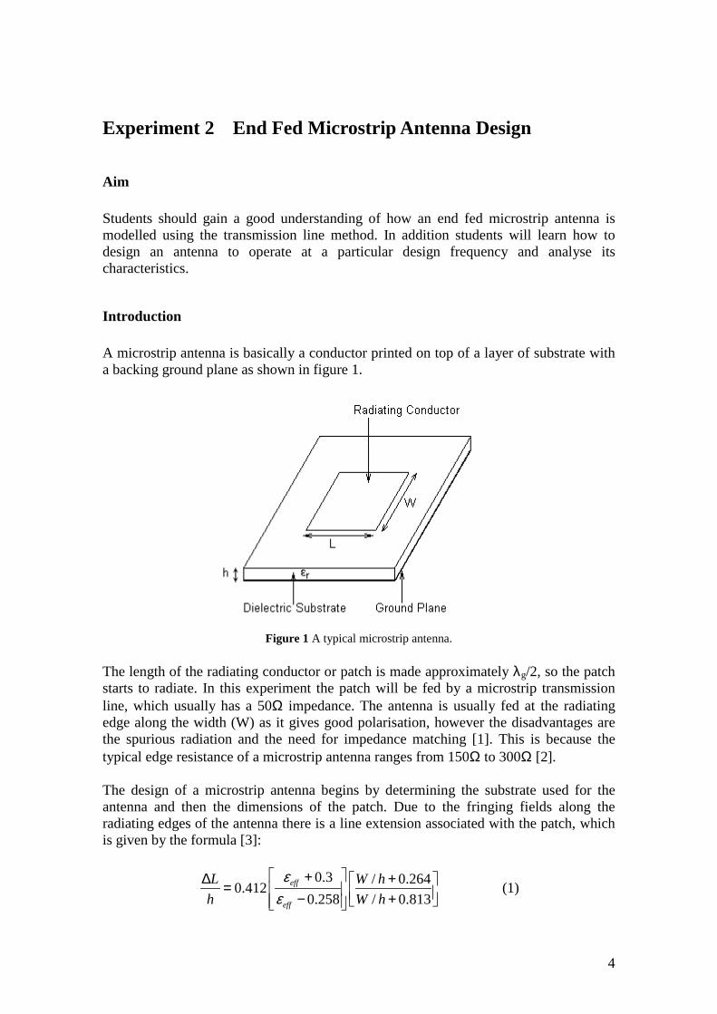
A microstrip antenna is basically a conductor printed on top of a layer of substrate witha backing ground plane as shown in figure 1.
Figure 1 A typical microstrip antenna.
The length of the radiating conductor or patch is made approximately λg/2, so the patchstarts to radiate. In this experiment the patch will be fed by a microstrip transmissionline, which usually has a 50Ω impedance. The antenna is usually fed at the radiatingedge along the width (W) as it gives good polarisation, however the disadvantages arethe spurious radiation and the need for impedance matching [1]. This is because thetypical edge resistance of a microstrip antenna ranges from 150Ω to 300Ω [2].
The design of a microstrip antenna begins by determining the substrate used for theantenna and then the dimensions of the patch. Due to the fringing fields along theradiating edges of the antenna there is a line extension associated with the patch, whichis given by the formula [3]:
0.3 / 0.2640.4120.258 / 0.813
eff
eff
L W hh W h
εε +∆ + = − +
(1)

5
The effective dielectric constant (εeff) due to the air dielectric boundary is given by [3]:
121 1 101
2 2r r
effh
Wε εε
−+ − = + +
(2)
The resonant frequency can be estimated by using the formula [2]:
( )1
2 2ro o eff
fL Lµ ε ε
=+ ∆
(3)
Where: µo = permeability of free spaceεo = permittivity of free space∆L = line extensionεeff = effective dielectric constant
Estimation of width and length
By choosing the substrate, the width and length of the patch can be estimated. An initialapproximation for the length can be made for a half wave microstrip antenna radiated bythe formula:
L = 0.48λg ~0.49λg (4)
Where: gr r
cf
λε
=
The width (W) is usually chosen such that it lies in the ratio, L < W < 2L for goodradiation characteristics, if W is too large then higher order modes will move closer tothe design frequency.
Radiation characteristics: A microstrip antenna is basically a broadside radiator, whichhas a relatively large beamwidth and low, gain characteristics. The formulas for the Eand H plane radiation patterns are given by [3]:
E-plane:sin cos
2( ) cos cos2cos
2
o
o
o
k hk LF k h
θθ θ
θ
=
(5)
H-Plane:sin cos sin
2( )cos
2
o
o
k W
F k W
φ φφ
φ
= (6)

6
Where: ko = 2p/lo (free space wavenumber)
*Note: Equations (1) to (4) are only approximate formulas and numerical analysis usinga full wave analysis package such as Mstrip40 is necessary.
Experiment
1. Design a microstrip antenna to operate at 1.8GHz given the substrate used in thedesign is FR4 PCB material with the following parameter:εr = 4.6tanδ = 0.022h = 1.6mmcopper thickness = 35µm
A program, using equations 1 to 3, can be written which calculates the resonantfrequency of an antenna using estimates for W, L and for a given h, εr.
2. After determining the patch dimensions L and W, the feed line can be estimatedusing closed form equations in microstrip transmission line text books or using acommercially free program found on the website [4].
3. Draw the design on the Mstrip40 structure file, the file Demo1 can used as atemplate for the design. Remember to change the dielectric properties, segmentsizes and frequency simulation range to suit your design. The file must be savedeach time alterations are made or else it will not simulate the any of the changedparameters.
4. Observe the smith chart what kind of bandwidth characteristics does the end fedantenna possess?
5. Plot the theoretical E-plane microstrip antenna radiation pattern given inequation 5 and compare it with the simulated Mstrip40 radiation plot.
6. If the student is satisfied with the design then if there are materials available inthe laboratory then students can build their own antenna (see the section in themanual about antenna design)
Further Investigation
Try and redesign the antenna by using low loss substrates such as Rogers RT/Duriodmaterial, Taconic TLX substrates etc.
Vary the height of the antenna substrate and observe the effects on the impedance plotand the bandwidth, are there any improvements?
A stacked configuration can be designed by invoking the STRUKTU command andadding another dielectric layer, see the Mstrip40 user manual for details.

7
Experiment 3 Inset Fed Microstrip Antenna Design
Aim
To design a matched microstrip antenna by using an inset feed configuration.
Introduction
In most microstrip end fed antennas the feed line impedance (50Ω) is always the sameas the radiation resistance at the edge of the patch, which is usually a few hundred ohmsdepending on the patch dimensions and the substrate used. As a result this inputmismatch will affect the antenna performance because maximum power is not beingtransferred. When a matching network is implemented on the feed network thisimproves the performance of the antenna as there are less reflections.
A typical method used to match the antenna is the use of an inset feed, because theresistance varies as a cosine squared function along the length of the patch a 50Ω can befound which is a distance from the edge of the patch [5]. This distance is called the insetdistance. A diagram of an inset fed patch is shown in figure 1, where xo represents theinset length:
Figure 1 Inset fed patch.
The analysis of the inset fed patch is summarised from the references [6] and [7] whichuses a transmission line model network to analyse the antenna.

8
Figure 2 Transmission line network model of a rectangular patch antenna.
When the antenna resonates (L~λg/2), the total admittance becomes real and iscalculated using the formula:
Yin = Y1 + Y2 (1) = 2G1
The input impedance is calculated using the formula:
1
1 12in
in
ZY G
= = (2)
However the above equation for input impedance does not take into consideration themutual coupling between the radiating slots, so we can redefine the input resistance:
( )1 12
12inR
G G=
±(3)
Where: G12 = mutual conductance G1 = self conductance. + = odd resonant modes – = even resonant modes
The self conductance can be calculated using the following expressions [9]:
11 2120
IGπ
= (4)

9
Where I1 is the integral defined by:
( ) ( ) ( )
2
31 0
sin cos2 sin
cos
sin2 cos
o
i
k W
I d
XX XS X
X
πθ
θ θθ
=
= − + + +
∫
(5)
Where: X = koW ko = 2π/λo Si = sin integral
The mutual conductance G12 is calculated using the following expression [10]:
( )
2
312 2 0
sin cos1 2 sin sin
120 cos
o
o o
k W
G J k L dπ
θθ θ θ
π θ
=
∫ (6)
Were: Jo = Bessel function of the first kind
The input resistance for an inset fed patch is given by the simplified expression [11]:
2
1 12
1( ) cos2( )
oin o
xR x xG G L
π = = + (7)
Where: xo = the inset feed distance
When xo = 0, then the resistance at the edge of the patch can be found:
1 12
1( 0)2( )in oR x
G G= =
+(8)
The optimum value of xo, (Rin = 50 Ω), can be found using equations 4 to 7. Theresistance at the edge of the patch can be used to design a matching network for theantenna.
Preliminary
Students should attempt experiment 2 before they start experiment 3, so they do notneed to recalculate the dimensions of the patch.

10
Experiment
1. Use a mathematical package such as Maple of Matlab to design a program thatestimates the required inset feed distance for a Rin = 50Ω. Run the program tofind the optimum inset distance.
2. Use the STR file from experiment 2 and modify it so the inset is implementedsimilar to figure 1. The size of the segment sizes in the x-direction my need to beadjusted to draw the inset distance accurately. The width of the inset, either sideof the feed line, is usually made the same as the feed line.
3. Once the STR has been finished then simulate the file in Mstrip40.
4. Observe the outputs such as the smith chart, feed current and radiation pattern,how do the compare to the end fed design in experiment 2. Plot the VSWR byusing the data in the SNP file.
5. The last step is the construction of the antenna when the student is satisfied withthe design.
Further Investigation
Design a single stub matching circuit using a smith chart instead of using an inset feedand compare the results. The 50Ω feed line impedance should be matched to theresistance at the edge of the patch using equation 8. Remember to use open-circuitedstubs in the design as Mstrip40 does not model loads.
Students should be familiar with the single stub matching technique if not they shouldread up on the literature [12] and [13].
Other matching techniques employing microstrip lines taught in class or in the literaturecan be designed and implemented simulated in Mstrip40 to compare the bandwidth.

11
Experiment 4 Proximity Fed Microstrip Antenna Design
Aim
To analyse and design a proximity coupled microstrip antenna.
Introduction
Electromagnetically coupled (EMC) designs such as proximity coupled and aperture fedantennas have many advantages over end fed and coaxial fed antennas. Someadvantages include:
• No physical contact between feed line and radiating element.• No drilling required.• Less spurious radiation.• Better for array configurations.• Good suppression of higher order modes.• Better high frequency performance.
A proximity-coupled antenna consists of two layers: it has a feed layer which is just a50Ω microstrip line with a backing ground plane and the upper layer is the mainradiating patch. Here is a diagram of the proximity coupled antenna:
Figure 1 Proximity coupled antenna
The equivalent circuit diagram of the structure is shown on the next page [14]:

12
Figure 2 Equivalent circuit of a proximity coupled antenna at the patch edge.
The main radiating patch is represented by a parallel resonant (RLC) circuit, with thefeed line represented by the coupling capacitance Cc. The level of coupling can beadjusted by varying the length of the overlap distance S in figure 1. Maximum couplingoccurs when the overlap distance is approximately half of the patch length.
In a typical design the resonant frequency usually shifts up by 1 to 2% for an overlap ofL/2 so the dimensions of the radiating patch should be designed at a lower frequency[14].
The theory behind EMC patches is quite complex and only design guidelines will bepresented in this experiment for interested students they can refer to the literature [15].
Experiment
1. Calculate the dimensions for the upper layer by using the methods in experimentto determine the patch dimensions for a square patch (L = W) to resonate at1.8GHz using FR4 PCB substrate:εr = 4.6tanδ = 0.022h = 1.6mmcopper thickness = 35µm
2. Determine the width of the 50Ω line for the feed line for the bottom layer.3. Draw the geometry of the proximity coupled patch in the STR file in Mstrip40.
The files DEMO6 and DEMO7 can be used as templates for the design.Remember to choose the appropriate segment sizes, excitation frequency andsubstrate parameters.
4. Simulate the design.
5. How does the impedance locus change on the smith chart?

13
6. Try and increase the precision of the program by setting the radius to 30 andintegration accuracy to 4. Is there any difference compared with previousresults?
Further Investigation
Vary the inset feed distance by making the offset larger what is the effect on thecoupling? Now try and decrease the offset simulate the design and note the results.

14
Experiment 5 Aperture Fed Microstrip Antenna Design
Aim
To design an aperture fed microstrip antenna.
Introduction
In an aperture coupled feed, which is another type of EMC feed, the RF energy from thefeed line is coupled to the radiating element through a common aperture in the form of arectangular slot. This type of feed was first proposed by Pozar in 1985 [16]. Theaperture coupled feeding mechanism is shown in figure 1:
Figure 1 Aperture coupled feed [17].
In this design we will concentrate on the design of this antenna rather than the theory,for students interested in finding more about aperture fed antenna they should consultthe references: [18] and [19].

15
Aperture fed antenna design parameters
There are various parameters, which may be varied in an aperture fed design, which canbe used to tune the antenna [17]:
• Slot length (La): this parameter determines the coupling level to the upper patch aswell as the back radiation level, and should be optimised for impedance matching.Typical lengths for the slot length are 0.082λo for low dielectric constants (εr = 2.54)and 0.074λo for high dielectric constants (εr = 10.2) [20].
• Slot width (Wa): the width of the slot affects the coupling level however does nothave a very large effect, the slot width is usually made 1/10×slot length.
• Feed line width (Wf): determines the characteristic impedance of the feed line,which is usually 50Ω.
• Position of the patch relative to the slot: for maximum coupling the patch should becentred over the slot. Moving the patch relative to the slot in the H-plane (y-direction) has little effect on the input impedance, whereas moving the patch patchrelative to the slot in the E-plane (x-direction) decreases the coupling.
• Length of open circuited stub (Ls): used to tune out the reactance of the slot and isusually made slightly less than λg/4
The parameters that are usually optimised in aperture fed designs are the slot length andopen circuited stub length. The size of the impedance locus is determined by the slotlength, when the slot length is increased the diameter of the locus becomes larger due tothe increase in coupling. The length of the stub rotates the input impedance locus and isused to compensate for the inductance of the slot and patch and helps create a realimpedance for the patch.
Experiment
1. Design an aperture fed antenna for the following antenna properties:Substrate = RO4003
εr = 3.38tanδ = 0.0021 (tested at 2.5GHz)h = 1.524mmcopper thickness = 17.5µm
Design Frequency = 1.8GHzFrom this data the dimensions of the radiating patch (square) and feed line width(50Ω) can be calculated.
The design guidelines to estimate the antenna parameters such as:• Slot length• Slot width

16
• Length of the open circuited stub
2. Draw up the structure with the parameters calculated in part 1 in Mstrip40 usingDEMO11 as a template, make sure the slot option is chosen.
3. Simulate the design, the precision of the integration needs to be increased due tothe coupling from the slot. The simulation may take a long time due to theincreased precision.
4. Look at the smith chart and radiation pattern output how do the results comparewith the proximity fed design.
5. Try vary the slot dimensions and observe the effect of the smith chart.
6. Now vary the length of the open circuited stub (end of the feed line) and note theresults.
Further Investigation
Redesign the antenna using different substrates and observe the difference on theradiation plot. Foam (εr = 1.0) can be used in the upper substrate, layer 3 to try andimprove the bandwidth.
A dielectric layer can be added on the main radiating patch (randome) to observe thechange in the resonant frequency.
17
Experiment 6 Microstrip Antenna Array Design
AimIn this experiment a log periodic antenna array will be analysed and designed.
Introduction
Microstrip antennas that operate as a single element usually have a relatively large halfpower beamwidth, low gain and low radiation efficiency. In order to improve on theseparameters, microstrip antennas are used in array configurations to improve the gain andrange of the radiating structure.
There are many effects such as mutual coupling between elements which must be takeninto consideration when analysing array structure. As a result full wave analyses areusually used to model arrays.
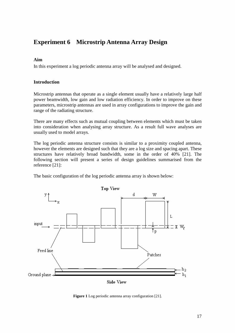
The log periodic antenna structure consists is similar to a proximity coupled antenna,however the elements are designed such that they are a log size and spacing apart. Thesestructures have relatively broad bandwidth, some in the order of 40% [21]. Thefollowing section will present a series of design guidelines summarised from thereference [21]:
The basic configuration of the log periodic antenna array is shown below:
Figure 1 Log periodic antenna array configuration [21].

18
The length, width and spacing between patches (d) is given by the expression
1 1 1m m m
m m m
L W dL W d
τ + + += + + (1)
Where: τ = scale factor.
The height of both the substrate layers and feed line width should be kept constant.
Here are the basic guidelines for the design:• Select the substrate layers.• Determine the upper or lower patch length then using equation 1 to find all the
corresponding patch widths and element distances.• For the initial patch the width is chosen such that W=0.8×L, to prevent higher order
modes.• Find the number of patches (M) required which is the ratio of the desired
bandwidth:
( )( )
BW DesiredM
BW Single Patch= (2)
• The input return loss or bandwidth can be improved by changing the patch spacing,d.
• The value for d is usually very close to the length L so for the initial design a “d” ofaround d = 1.05×L can be used as an initial estimate then varied in the simulation todetermine the optimum spacing.
The above design steps should only be used as a guide to log periodic antenna arraydesign, and are simplified for learning purposes, for a very thorough analysis of the logperiodic microstrip antenna array refer to the literature [21].
Experiment
1. Design a log periodic antenna array using the following parameters:Layer 1 and 2 are FR4 with the following properties.εr = 4.6tanδ = 0.022h = 1.6mmcopper thickness = 35µmDesign the array to have a centre frequency of 1.8GHz.Use a scale factor of τ = 1.05.
2. Find the number of patches (M) given you want an 8% desired bandwidth.
3. Find the dimensions of the patch for upper frequency or lower frequency thenuse equation 1 to determine the size of the other elements.

19
4. Once the dimensions are found draw the design up in the STR file a proximitycoupled design used in experiment 4 can be used as template. Choose thesegment size to give you the best accuracy. Initially try a spacing betweenpatches of one x-directed segment size.
5. Simulate the design.
6. Look at the input impedance plot on the smith chart is the antenna matched?
7. Open the radiation pattern window compare the pattern and gain with theprevious antenna designs. Is the radiation pattern symmetrical?
Further Investigation
Try and design other array structures using coplanar feeds rather than a proximitycoupled feed.
Include matching elements on the feed line to try and improve the input return loss ofthe array.
Design a log periodic array with more elements to try and improve the bandwidth andgain.

20
Future Experiments
Additional experiments that students can undertake are the following:
• Design of antennas employing foam substrates to improve the bandwidth.• Design of slot antennas• Further array investigation• Circularly polarised antennas
Many of the demo files contained in Mstrip40 such as Demo17 and Demo20 can befurther researched.
The design of novel antenna designs are only limited by a student’s creativity so thereare many other arbitrary patch shapes which can be analysed and designed usingMstrip40.

21
Practical Antenna Design
Over the course of my project I have gained skills in microstrip patch antennamanufacture using basic printed circuit manufacturing techniques. Here are the basicguidelines for producing your own rectangular microstrip antenna:
1 Choose your antenna substrate, normal PCB material will be fine for frequenciesbelow 1 GHz.
2 Design the antenna using experiment 2 or some other method.3 Once you are happy draw up the artwork of the antenna on Protel or another
program, which will print out the design in a 1:1 scale.4 Print the design on transparent film (ask lab technicians and lecturers for
details.)5 Expose the design under UV light with the design on the film covering the
substrate area you want the design to appear on.6 Create a developer solution to remove the photoresist.7 Place the antenna in the etching tank to remove the unwanted copper.8 Once the antenna is finished then you can solder a connector on the feed line and
then test it.

22
Antenna Testing
Here is a description of some basic methods, which are used to test the variousmicrostrip antenna parameters.
Impedance measurements
Network AnalyserInput Impedance characteristics
Smith Chart plot analysisSWR analysis
s12, s21 transmission characteristics
Radiation measurements
Preferably done in an anechoic chamberCan use a simple set up with the following equipment:Signal generator (transmitter)Spectrum analyser (receiver)Set up which will rotate the antenna 360o.
Alternatively use a network analyser and connect the transmitting antenna to one port(s11) and receiving antenna to the output port (s22).
By moving the antenna at different angles and taking power measurements using thereceiver (spectrum analyser or network analyser), a plot of the radiation pattern can beobtained. Cross-polarisation measurements can be made by changing the field plane ofthe receiving antenna. The gain of the antenna can be measured using various methodsdescribed in the literature [22] and [23].

23
References
[1] Pozar, D.M. and Schaubert D.H. Microstrip Antennas. United States of America.IEEE Press 1995., p 62.
[2] Balanis, C.A. Antenna Theory Analysis and Design, Second Edition. UnitedStates of America. John Wiley & Sons 1997., p734.
[3] Bhartia P., et al. Millimeter-Wave Microstrip and Printed Circuit Antennas.Norwood, Mass. Artech House 1991, p10.
[4] TX-Linehttp://www.appwave.com/products/txline.html
[5] K.R. Carver and J.W. Mink, “Microstrip Antenna Technology,” IEEE Trans.Antennas Propagat., vol. AP-29, no.1, pp 2-24, Jan. 1981.
[6] James J.R., P.S. Hall and C. Wood. Microstrip Antenna Theory and Design.London, United Kingdom. Peter Peregrinus 1981., pp 87-89.
[7] Balanis, C.A. Op Cit. pp730-734.
[9] Balanis, C.A. Op Cit. p732.
[10] James J.R., P.S. Hall and C. Wood. Op cit. p88.
[11] Balanis, C.A. Op Cit. p734.
[12] Gonzalez, G. Microwave Transistor Amplifiers Analysis and Design, Secondedition, Prentice Hall, 1997.pp152-162.
[13] Ludwig, R and Bretchko, P. RF Circuit Design Theory and Applications,Prentice Hall, 2000. pp435-438
[14] Sainati, R.A. CAD of Microstrip Antennas for Wireless Applications. Norwood,Mass. Artech House 1996, p 87.
[15] Georg Splitt, Recent Publicationshttp://www.e-technik.fh-kiel.de/~splitt/html/papers.htm
[16] D. M. Pozar, “A Microstrip Antenna Aperture Coupled to a Microstrip Line”,Electronics Letters, Vol. 21, pp 49-50, January 17, 1985.
[17] “A Review of Aperture Coupled Microstrip Antennas: History, Operation,Development, and Applications.”http://www.ecs.umass.edu/ece/pozar/aperture.pdf

24
[18] P.L Sullivan and D.H. Schaubert, “Analysis of an Aperture Coupled MicrostripAntenna,” IEEE Trans. Antennas Propagat., vol. AP-34, pp 997-984, Aug 1986.
[19] Garg R. et al, Microstrip Antenna Design Book. Norwood, Mass. Artech House2001, p 539-550.
[20] Sainati, R.A. Op cit, p 96.
[21] P.S. Hall, “Multioctave bandwidth log-perodic microstrip antenna array,” IEEProc., vol.133, Part H, pp127-136, April 1986.
[22] Macnamara, T. Handbook of Antennas for EMC. Norwood, Mass. Artech Housepp221-234.
[23] Zurcher, J,-F, et al. Broadband Patch Antennas. Norwood, Mass. Artech House1995, pp 184-188.
Related Documents