Hardware Training Tools Data Acquisition I/O Cards Development Tools Pic Tutor Software CAD Education Consulting Downloads PRICE LIST Corporate About AMS Chronology Contact Sales Offices US International Publication EBOOKS Articles Press Release CAE Glossary Design Guidelines PCB FABRICATION Resource Resource Page EZMicro Resource Support Registration Support Payment Terms Site Designed by GlobalAMS 8255 CHIPS The 8255A is a programmable peripheral interface (PPI) device designed for use in Intel microcomputer systems. Its function is that of a general purposes I/O component to Interface peripheral equipment to the microcomputer system bush. The functional configuration of the 8255A is programmed by the systems software so that normally no external logic is necessary to interface peripheral devices or structures. Data Bus Buffer This 3-stable bi-directional 8-bit buffer is used to interface the 8255A to the systems data bus. Data is transmitted or received by the buffer upon execution of input or output instructions by the CPU. Control words and status information are also transferred through the data bus buffer. Read/Write and Control Logic The function of this block is to manage all of the Internal and External transfers of both Data and Control or Status words. It accepts inputs from the CPU Address and Control business and in turn, issues commands to both of the Control Groups. (CS) Chip Select. A “low’ on this input pin enables the communication between the 8255A, and the CPU. (RD) Read. A “low” on this Input pin enables the 8255A to send the data or status information to the CPU on the data bus. In essence, it allows the CPU to “read from the 8255A. Page 1 of 18 Engineering and Training Tools 4/11/2011 http://www.advancedmsinc.com/iocards/8255.htm

Welcome message from author
This document is posted to help you gain knowledge. Please leave a comment to let me know what you think about it! Share it to your friends and learn new things together.
Transcript

Hardware Training ToolsData AcquisitionI/O CardsDevelopment ToolsPic Tutor
SoftwareCADEducationConsultingDownloads
PRICE LIST
Corporate About AMSChronologyContact
Sales Offices USInternational
PublicationEBOOKSArticlesPress ReleaseCAE GlossaryDesignGuidelinesPCB FABRICATION
ResourceResource PageEZMicroResource
SupportRegistrationSupportPaymentTerms
Site Designed by
GlobalAMS
8255 CHIPS
The 8255A is a programmable peripheral interface (PPI) device designed for use in Intel microcomputer systems. Its function is that of a general purposes I/O component to Interface peripheral equipment to the microcomputer system bush. The functional configuration of the 8255A is programmed by the systems software so that normally no external logic is necessary to interface peripheral devices or structures.
Data Bus BufferThis 3-stable bi-directional 8-bit buffer is used to interface the 8255A to the systems data bus. Data is transmitted or received by the buffer upon execution of input or output instructions by the CPU. Control words and status information are also transferred through the data bus buffer.
Read/Write and Control LogicThe function of this block is to manage all of the Internal and External transfers of both Data and Control or Status words. It accepts inputs from the CPU Address and Control business and in turn, issues commands to both of the Control Groups.
(CS)
Chip Select. A “low’ on this input pin enables the communication between the 8255A, and the CPU.
(RD)
Read. A “low” on this Input pin enables the 8255A to send the data or status information to the CPU on the data bus. In essence, it allows the CPU to “read from the 8255A.
Page 1 of 18Engineering and Training Tools
4/11/2011http://www.advancedmsinc.com/iocards/8255.htm
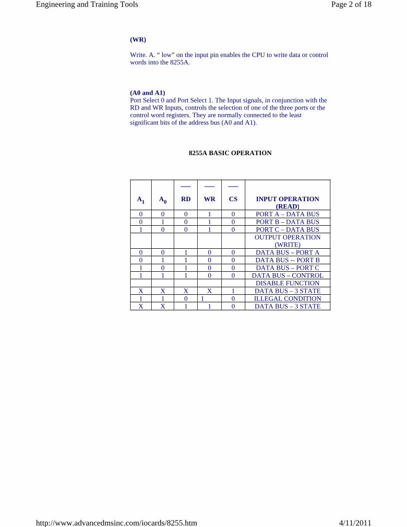
(WR)
Write. A. “ low” on the input pin enables the CPU to write data or control words into the 8255A.
(A0 and A1)Port Select 0 and Port Select 1. The Input signals, in conjunction with the RD and WR Inputs, controls the selection of one of the three ports or the control word registers. They are normally connected to the least significant bits of the address bus (A0 and A1).
8255A BASIC OPERATION
A1 A0
___
RD
___
WR
___
CS INPUT OPERATION (READ)
0 0 0 1 0 PORT A – DATA BUS0 1 0 1 0 PORT B – DATA BUS1 0 0 1 0 PORT C – DATA BUS
OUTPUT OPERATION (WRITE)
0 0 1 0 0 DATA BUS – PORT A0 1 1 0 0 DATA BUS -- PORT B1 0 1 0 0 DATA BUS – PORT C1 1 1 0 0 DATA BUS – CONTROL
DISABLE FUNCTIONX X X X 1 DATA BUS – 3 STATE1 1 0 1 0 ILLEGAL CONDITIONX X 1 1 0 DATA BUS – 3 STATE
Page 2 of 18Engineering and Training Tools
4/11/2011http://www.advancedmsinc.com/iocards/8255.htm

Figure 3. 8255 A Block Diagram Showing Data Bus Buffer and Read/Write Control Logic Functions
(RESET)
Reset. A “high” on this Input clears the control register and all ports (A, B, C) are set to the Input mode.
Group A and Group B ControlsThe functional configuration of each port is programmed by the systems software. In essence, the CPU “output” a control word to the 8255A. The control word contains information such as “mode”, bit set”, bit reset”, etc. that Initializes the functional configuration of the 8255A.
Each of the Control blocks (Group A and Group B) accepts commands from the Read/Write Control Logic, receives control words from the internal data bus and issues the proper commands to its associated ports.
Control Group A – Port A and Port C upper (C7 C4)
Control Group B – Port B and Port C lower (C3 C0)
The Control Word Register can only be written into. No.
Read operation of the Control Word Register is allowed.
Ports A, B, and CThe 8255A contains three 8-bit ports (A , B, and C). All can be
Page 3 of 18Engineering and Training Tools
4/11/2011http://www.advancedmsinc.com/iocards/8255.htm

configured in a wide variety of functional characteristics by the system software but each has its own special features or personally to further enhance the power and flexibility of the 8255A.
Port A. One 8 bit data output latch/buffer and one 8-bit data input latch.
Port B. One 8-bit data output latch/buffer and one 8-bit data input buffer.
Port C. One 8-bit data output latch/buffer and one 8-bit data input buffer (no latch for input). This port can be divided into two 4-bit ports under the mode control. Each 4-bit port contains a 4-bit latch and it can be used for the controls signal outputs and status signal inputs in conjunction with ports A and B.
Page 4 of 18Engineering and Training Tools
4/11/2011http://www.advancedmsinc.com/iocards/8255.htm

D7 – D0 DATA BUS DIRECTIONAL
RESET RESET INPUTCS CHIP SELECTRD READ INPUTWR WRITE INPUTA0 – A1 PORT ADDRESSPA 7 PA 0 PORT A (BIT)PB 7 PB 0 PORT B (BIT)PC 7 PC 0 PORT C (BIT)Vcc 5 VOLTSGND 0 VOLTS
8255A OPERATIONAL DESCRIPTION
Mode SelectionThere are three basic modes of operation that can be selected by the systems software:
Mode O – Basic Input/Output
Mode 1 – Strobed Input/Output
Mode 2 – Bi-Directional Bus
Page 5 of 18Engineering and Training Tools
4/11/2011http://www.advancedmsinc.com/iocards/8255.htm
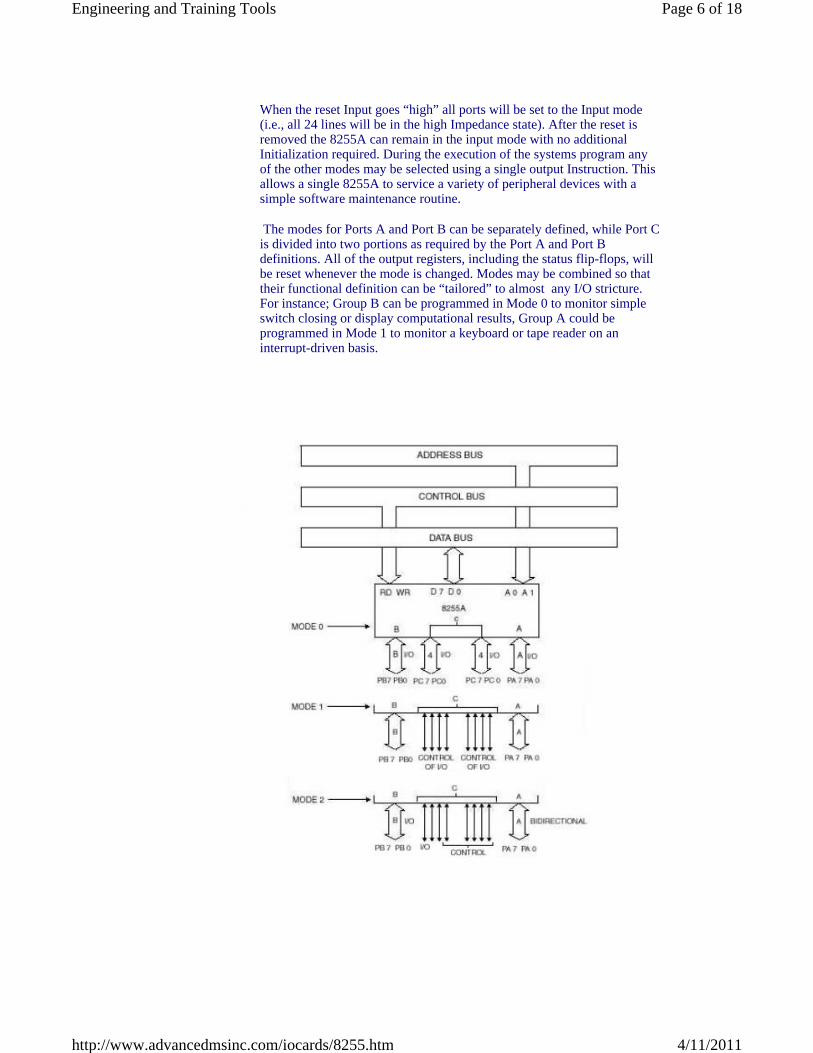
When the reset Input goes “high” all ports will be set to the Input mode (i.e., all 24 lines will be in the high Impedance state). After the reset is removed the 8255A can remain in the input mode with no additional Initialization required. During the execution of the systems program any of the other modes may be selected using a single output Instruction. This allows a single 8255A to service a variety of peripheral devices with a simple software maintenance routine.
The modes for Ports A and Port B can be separately defined, while Port C is divided into two portions as required by the Port A and Port B definitions. All of the output registers, including the status flip-flops, will be reset whenever the mode is changed. Modes may be combined so that their functional definition can be “tailored” to almost any I/O stricture. For instance; Group B can be programmed in Mode 0 to monitor simple switch closing or display computational results, Group A could be programmed in Mode 1 to monitor a keyboard or tape reader on an interrupt-driven basis.
Page 6 of 18Engineering and Training Tools
4/11/2011http://www.advancedmsinc.com/iocards/8255.htm
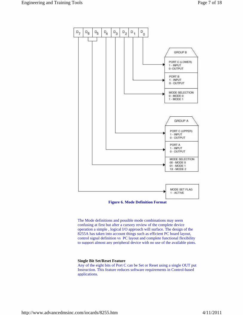
Figure 6. Mode Definition Format
The Mode definitions and possible mode combinations may seem confusing at first but after a cursory review of the complete device operation a simple , logical I/O approach will surface. The design of the 8255A has taken into account things such as efficient PC board layout, control signal definition vs PC layout and complete functional flexibility to support almost any peripheral device with no use of the available pints.
Single Bit Set/Reset FeatureAny of the eight bits of Port C can be Set or Reset using a single OUT put Instruction. This feature reduces software requirements in Control-based applications.
Page 7 of 18Engineering and Training Tools
4/11/2011http://www.advancedmsinc.com/iocards/8255.htm

When Port C is being used as status/control for Port A or B these Bits can be set or reset by using the Bit set/reset operation just as if they were data output port.
Interrupt Control FunctionsWhen the 8255A is programmed to operate in mode 1 or mode 2, control signals are provided that can used as interrupt request input to the CPU. The interrupt request signal generated from port C, can be inhibited or enabled by setting or resetting the associated INTE flip-flop, using the bit set/reset function of port C.
This function allows the Programmer to disallow or allow a specific I/O device to interrupt the CPU without affecting any other device in the interrupt structure.
INTE flip-flop definition
(BIT-SET) – INTE is SET – Interrupt enable
(BIT-RESET) – INTE is RESET – Interrupt disable
Note: All Mask flip-flops are automatically reset during mode selection
Page 8 of 18Engineering and Training Tools
4/11/2011http://www.advancedmsinc.com/iocards/8255.htm

and device reset.
Operating ModesMode 0 (Basic Input/Output). This functional configuration provides simple input operations for each of the three ports. No “handshaking” is required data is simply written to or read from a specified port.
Mode O Basic Functional Definitions:
� Two 8-bit ports and two 4-bit port� Any port can be input or output.� Outputs are not latched.� Inputs are not latched.� 16 different Input/output configurations are not possible in this
Mode.
A B GROUP A GROUP BD4 D3 D2 D1 PORT A PORT C
(UPPER)
# PORT B PORT C
(LOWER)0 0 0 0 OUTPUT OUTPUT 0 OUTPUT OUTPUT0 0 0 1 OUTPUT OUTPUT 1 OUTPUT INPUT0 0 1 0 OUTPUT OUTPUT 2 INPUT OUTPUT0 0 1 1 OUTPUT OUTPUT 3 INPUT INPUT0 1 0 0 OUTPUT INPUT 4 OUTPUT OUTPUT0 1 0 1 OUTPUT INPUT 5 OUTPUT INPUT0 1 1 0 OUTPUT INPUT 6 INPUT OUTPUT0 1 1 1 OUTPUT INPUT 7 INPUT INPUT1 0 0 0 INPUT OUTPUT 8 OUTPUT OUTPUT1 0 0 1 INPUT OUTPUT 9 OUTPUT INPUT1 0 1 0 INPUT OUTPUT 10 INPUT OUTPUT1 0 1 1 INPUT OUTPUT 11 INPUT INPUT1 1 0 0 INPUT INPUT 12 OUTPUT OUTPUT1 1 0 1 INPUT INPUT 13 OUTPUT INPUT1 1 1 0 INPUT INPUT 14 INPUT OUTPUT1 1 1 1 INPUT INPUT 15 INPUT INPUT
Mode 0 Configuration
Page 9 of 18Engineering and Training Tools
4/11/2011http://www.advancedmsinc.com/iocards/8255.htm

Page 10 of 18Engineering and Training Tools
4/11/2011http://www.advancedmsinc.com/iocards/8255.htm

Operating Modes
MODE 1 (Strobed Input/Output). This functional configuration provides a
Page 11 of 18Engineering and Training Tools
4/11/2011http://www.advancedmsinc.com/iocards/8255.htm

means for transferring I/O data to or from a specified port in conjunction with strobes or “handshaking” signals. In mode 1, port A and Port B use the lines on port C to generate or accept these “handshaking” signals.
Mode 1 Basic Functional Definitions:
� Two groups (Group A and Group B)� Each group contains one 8-bit data port and one 4-bit control/data
port� The 8-bit data port can be either Inputs or output Both inputs and
outputs are latched.� The 4-bit port is used for control and status of the 8-bit data port.
Input Control Signal Definition
STB (Strobe Input). A “ low “ on the input loads data into the input latch.
IBF (Input Buffer Full F/F)
A “high” on this output indicates that the data has been loaded into the input latch. In essence, an acknowledgement.
IBF is set by STB input being low and is reset by the rising edge of the RD input.
INTR (Interrupt Request)
A “high” on this output can be used to interrupt the CPU when an input device is requesting service, INTR is set by the STB is a “one”, IBF is a “one “ and INTE is “one “. It is reset by the falling edge of RD. This procedure allows an input device to request service from the CPU by simply strobing its data into port.
INTE A
Controlled by bit set/reset of PC4
INTE B
Page 12 of 18Engineering and Training Tools
4/11/2011http://www.advancedmsinc.com/iocards/8255.htm

Controlled by set/reset PC2
Output Control Signal Definition
OBF (Output Buffer Full F/F). The OBF output will go “low” to indicate that the CPU has written data out to the specified port. The OBF F/F will be set by rising edge of the WR input being low.
ACK (Acknowledge Input). A “low” on this input informs the 8255A that the data from port A or port B has been accepted. In essence, a response from the peripheral device indicating that it has received the data output by CPU.
INTR (Interrupt Request). A “high” on the output can be used to interrupt the CPU when an output device has accepted data transmitted by the CPU. INTR is set when ACK is a “one”, OBF is a “one”, and INTE is a “one”. It is reset by the falling edge of WR.
INTE A
Controlled by bit set/reset of PC6.
INTE B
Controlled by bit
Page 13 of 18Engineering and Training Tools
4/11/2011http://www.advancedmsinc.com/iocards/8255.htm

set/reset of PC2.
Combination of MODE 1
Port A and B can be Individually defined as Input or output in Mode 1 to support a wide varlety of strobed I/O application.
Mode 2 (Strobed Bidirectional Bus I/O). This functional configuration provides a means for communicating with a peripheral device or structure on a single 8-bit bus for both transmitting and receiving data (bi-directional bus I/O). “Handshaking” signals are provided to maintain proper bus flow discipline in a similar manner to MODE.
1. Interrupt generation and enable/disable functions are also available.
Page 14 of 18Engineering and Training Tools
4/11/2011http://www.advancedmsinc.com/iocards/8255.htm
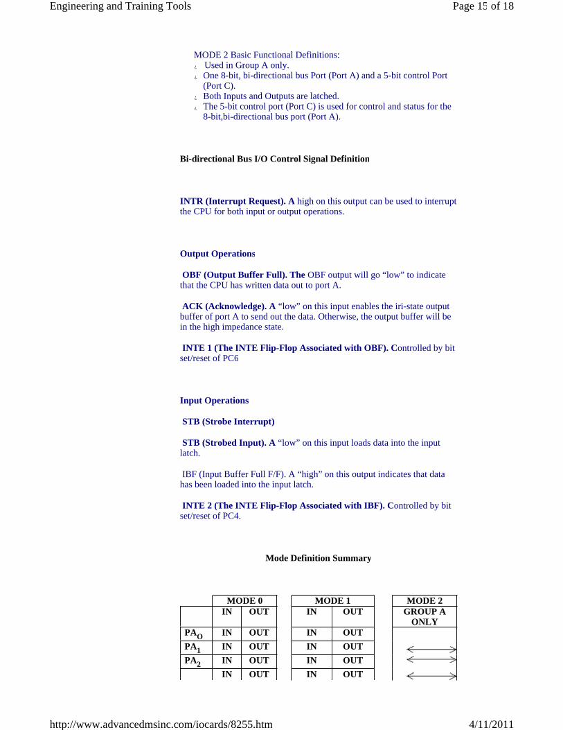
MODE 2 Basic Functional Definitions:� Used in Group A only.� One 8-bit, bi-directional bus Port (Port A) and a 5-bit control Port
(Port C).� Both Inputs and Outputs are latched.� The 5-bit control port (Port C) is used for control and status for the
8-bit,bi-directional bus port (Port A).
Bi-directional Bus I/O Control Signal Definition
INTR (Interrupt Request). A high on this output can be used to interrupt the CPU for both input or output operations.
Output Operations
OBF (Output Buffer Full). The OBF output will go “low” to indicate that the CPU has written data out to port A.
ACK (Acknowledge). A “low” on this input enables the iri-state output buffer of port A to send out the data. Otherwise, the output buffer will be in the high impedance state.
INTE 1 (The INTE Flip-Flop Associated with OBF). Controlled by bit set/reset of PC6
Input Operations
STB (Strobe Interrupt)
STB (Strobed Input). A “low” on this input loads data into the input latch.
IBF (Input Buffer Full F/F). A “high” on this output indicates that data has been loaded into the input latch.
INTE 2 (The INTE Flip-Flop Associated with IBF). Controlled by bit set/reset of PC4.
Mode Definition Summary
MODE 0 MODE 1 MODE 2IN OUT IN OUT GROUP A
ONLYPAO IN OUT IN OUT
PA1 IN OUT IN OUT
PA2 IN OUT IN OUT
IN OUT IN OUT
Page 15 of 18Engineering and Training Tools
4/11/2011http://www.advancedmsinc.com/iocards/8255.htm
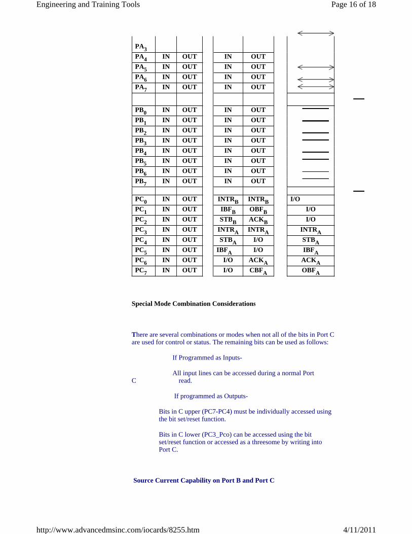
PA3PA4 IN OUT IN OUT
PA5 IN OUT IN OUT
PA6 IN OUT IN OUT
PA7 IN OUT IN OUT
PB0 IN OUT IN OUT
PB1 IN OUT IN OUT
PB2 IN OUT IN OUT
PB3 IN OUT IN OUT
PB4 IN OUT IN OUT
PB5 IN OUT IN OUT
PB6 IN OUT IN OUT
PB7 IN OUT IN OUT
PC0 IN OUT INTRB INTRB I/O
PC1 IN OUT IBFB OBFB I/O
PC2 IN OUT STBB ACKB I/O
PC3 IN OUT INTRA INTRA INTRAPC4 IN OUT STBA I/O STBAPC5 IN OUT IBFA I/O IBFAPC6 IN OUT I/O ACKA ACKAPC7 IN OUT I/O CBFA OBFA
Special Mode Combination Considerations
There are several combinations or modes when not all of the bits in Port C are used for control or status. The remaining bits can be used as follows:
If Programmed as Inputs-
All input lines can be accessed during a normal Port C read.
If programmed as Outputs-
Bits in C upper (PC7-PC4) must be individually accessed using the bit set/reset function.
Bits in C lower (PC3_Pco) can be accessed using the bit set/reset function or accessed as a threesome by writing into Port C.
Source Current Capability on Port B and Port C
Page 16 of 18Engineering and Training Tools
4/11/2011http://www.advancedmsinc.com/iocards/8255.htm

Any set of eight output buffers, selected randomly from Ports B and Ports C can source 1mA at 1.5volts. This feature allows the 8255A to directly drive Darlington type drivers and high-voltage displays that require such source current.
Reading Port C Status
In Mode O, Port C transfers data to or from the peripheral device. When the 8255 is programmed to function in Modes 1 or 2, Port C generates or accepts “hand shaking” signals with the peripheral device. Reading the contents of Port C allows the programmer to test or verify the “status” of each peripheral device and change the program flow accordingly.
There is co special instruction to read the status information from Port C. A normal read operation of Port C is executed to perform this function.
Figure 17. MODE 1 STATUS WORD FORMAT
INPUT CONFIGURATION
D7 D6 D5 D4 D3 D2 D1 D0
I/O I/O IBFA INTEA INTRA INTEB IBFB INTRB
OUTPUT CONFIGURATION
D7 D6 D5 D4 D3 D2 D1 D0
OBFA INTEA I/O I/O INTRA INTEB OBFB INTERB
Figure 18. Mode 2 Status Word Format
Page 17 of 18Engineering and Training Tools
4/11/2011http://www.advancedmsinc.com/iocards/8255.htm

Click here for More Info....
D7 D6 D5 D4 D3 D2 D1 D0OBFA INTE1 IBFA INTE2 INTRA
DEFINE BY MODE 0 MODE 1 SELECTION
Page 18 of 18Engineering and Training Tools
4/11/2011http://www.advancedmsinc.com/iocards/8255.htm
Related Documents