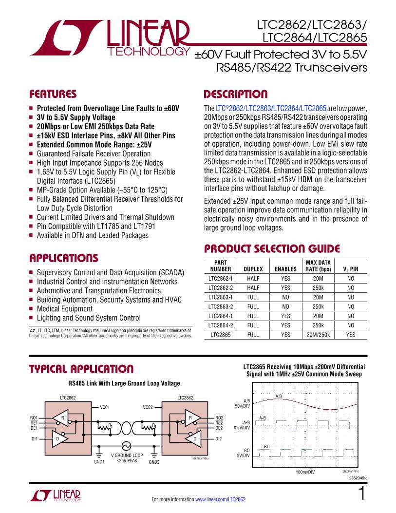
LTC2862/LTC2863/ LTC2864/LTC2865 1 2862345fc For more information www.linear.com/LTC2862 TYPICAL APPLICATION DESCRIPTION ±60V Fault Protected 3V to 5.5V RS485/RS422 Transceivers RS485 Link With Large Ground Loop Voltage FEATURES APPLICATIONS n Protected from Overvoltage Line Faults to ±60V n 3V to 5.5V Supply Voltage n 20Mbps or Low EMI 250kbps Data Rate n ±15kV ESD Interface Pins, ±8kV All Other Pins n Extended Common Mode Range: ±25V n Guaranteed Failsafe Receiver Operation n High Input Impedance Supports 256 Nodes n 1.65V to 5.5V Logic Supply Pin (V L ) for Flexible Digital Interface (LTC2865) n MP-Grade Option Available (–55°C to 125°C) n Fully Balanced Differential Receiver Thresholds for Low Duty Cycle Distortion n Current Limited Drivers and Thermal Shutdown n Pin Compatible with LT1785 and LT1791 n Available in DFN and Leaded Packages n Supervisory Control and Data Acquisition (SCADA) n Industrial Control and Instrumentation Networks n Automotive and Transportation Electronics n Building Automation, Security Systems and HVAC n Medical Equipment n Lighting and Sound System Control LTC2865 Receiving 10Mbps ±200mV Differential Signal with 1MHz ±25V Common Mode Sweep PART NUMBER DUPLEX ENABLES MAX DATA RATE (bps) V L PIN LTC2862-1 HALF YES 20M NO LTC2862-2 HALF YES 250k NO LTC2863-1 FULL NO 20M NO LTC2863-2 FULL NO 250k NO LTC2864-1 FULL YES 20M NO LTC2864-2 FULL YES 250k NO LTC2865 FULL YES 20M/250k YES The LTC ® 2862/LTC2863/LTC2864/LTC2865 are low power, 20Mbps or 250kbps RS485/RS422 transceivers operating on 3V to 5.5V supplies that feature ±60V overvoltage fault protection on the data transmission lines during all modes of operation, including power-down. Low EMI slew rate limited data transmission is available in a logic-selectable 250kbps mode in the LTC2865 and in 250kbps versions of the LTC2862-LTC2864. Enhanced ESD protection allows these parts to withstand ±15kV HBM on the transceiver interface pins without latchup or damage. Extended ±25V input common mode range and full fail- safe operation improve data communication reliability in electrically noisy environments and in the presence of large ground loop voltages. L, LT, LTC, LTM, Linear Technology the Linear logo and µModule are registered trademarks of Linear Technology Corporation. All other trademarks are the property of their respective owners. PRODUCT SELECTION GUIDE GND1 GND2 2862345 TA01a R t R t RO1 RE1 DE1 DI1 VCC1 LTC2862 LTC2862 VCC2 RO2 RE2 DE2 DI2 D D R R V GROUND LOOP ≤25V PEAK A,B 50V/DIV A-B 0.5V/DIV 100ns/DIV 2862345 TA01b RO 5V/DIV RO A,B A-B

Welcome message from author
This document is posted to help you gain knowledge. Please leave a comment to let me know what you think about it! Share it to your friends and learn new things together.
Transcript
LTC2862/LTC2863/LTC2864/LTC2865
12862345fc
For more information www.linear.com/LTC2862
Typical applicaTion
DescripTion
±60V Fault Protected 3V to 5.5VRS485/RS422 Transceivers
RS485 Link With Large Ground Loop Voltage
FeaTures
applicaTions
n Protected from Overvoltage Line Faults to ±60Vn 3V to 5.5V Supply Voltagen 20Mbps or Low EMI 250kbps Data Raten ±15kV ESD Interface Pins, ±8kV All Other Pinsn Extended Common Mode Range: ±25Vn Guaranteed Failsafe Receiver Operationn High Input Impedance Supports 256 Nodesn 1.65V to 5.5V Logic Supply Pin (VL) for Flexible
Digital Interface (LTC2865)n MP-Grade Option Available (–55°C to 125°C)n Fully Balanced Differential Receiver Thresholds for
Low Duty Cycle Distortionn Current Limited Drivers and Thermal Shutdownn Pin Compatible with LT1785 and LT1791n Available in DFN and Leaded Packages
n Supervisory Control and Data Acquisition (SCADA)n Industrial Control and Instrumentation Networksn Automotive and Transportation Electronicsn Building Automation, Security Systems and HVACn Medical Equipmentn Lighting and Sound System Control
LTC2865 Receiving 10Mbps ±200mV Differential Signal with 1MHz ±25V Common Mode Sweep
PART NUMBER
DUPLEX
ENABLES
MAX DATA RATE (bps)
VL PIN
LTC2862-1 HALF YES 20M NO
LTC2862-2 HALF YES 250k NO
LTC2863-1 FULL NO 20M NO
LTC2863-2 FULL NO 250k NO
LTC2864-1 FULL YES 20M NO
LTC2864-2 FULL YES 250k NO
LTC2865 FULL YES 20M/250k YES
The LTC®2862/LTC2863/LTC2864/LTC2865 are low power, 20Mbps or 250kbps RS485/RS422 transceivers operating on 3V to 5.5V supplies that feature ±60V overvoltage fault protection on the data transmission lines during all modes of operation, including power-down. Low EMI slew rate limited data transmission is available in a logic-selectable 250kbps mode in the LTC2865 and in 250kbps versions of the LTC2862-LTC2864. Enhanced ESD protection allows these parts to withstand ±15kV HBM on the transceiver interface pins without latchup or damage.
Extended ±25V input common mode range and full fail-safe operation improve data communication reliability in electrically noisy environments and in the presence of large ground loop voltages.
L, LT, LTC, LTM, Linear Technology the Linear logo and µModule are registered trademarks of Linear Technology Corporation. All other trademarks are the property of their respective owners.
proDucT selecTion GuiDe
GND1 GND22862345 TA01a
Rt Rt
RO1RE1DE1
DI1
VCC1
LTC2862 LTC2862
VCC2
RO2RE2DE2
DI2D D
R R
V GROUND LOOP≤25V PEAK
A,B50V/DIV
A-B0.5V/DIV
100ns/DIV 2862345 TA01b
RO5V/DIV
RO
A,B
A-B

LTC2862/LTC2863/LTC2864/LTC2865
22862345fc
For more information www.linear.com/LTC2862
absoluTe MaxiMuM raTinGs
Supply Voltages VCC............................................................. –0.3 to 6V VL .............................................................. –0.3 to 6V Logic Input Voltages (RE, DE, DI, SLO) .......... –0.3 to 6VInterface I/O: A, B, Y, Z .............................. –60V to +60VReceiver Output (RO) (LTC2862-LTC2864) ...................–0.3V to (VCC+0.3V)
Receiver Output (RO) (LTC2865) ..................................–0.3V to (VL + 0.3V)Operating Ambient Temperature Range (Note 4) LTC286xC ................................................ 0°C to 70°C LTC286xI .............................................–40°C to 85°C LTC286xH .......................................... –40°C to 125°C
LTC286xMP ....................................... –55°C to 125°CStorage Temperature Range .................. –65°C to 150°CLead Temperature (Soldering, 10 sec) ................... 300°C
pin conFiGuraTionLTC2862-1, LTC2862-2 LTC2862-1, LTC2862-2
1
2
3
4
8
7
6
5
TOP VIEW
VCC
B
A
GND
RO
RE
DE
DI
S8 PACKAGE8-LEAD (150mil) PLASTIC SO
TJMAX = 150°C, θJA = 150°C/W, θJC = 39°C/W
TOP VIEW
DD PACKAGE8-LEAD (3mm × 3mm) PLASTIC DFN
EXPOSED PAD (PIN 9) CONNECT TO PCB GNDTJMAX = 150°C, θJA = 43°C/W, θJC = 3°C/W
5
6
7
8
9
4
3
2
1RO
RE
DE
DI
VCC
B
A
GND
LTC2863-1, LTC2863-2 LTC2863-1, LTC2863-2
1
2
3
4
8
7
6
5
TOP VIEW
A
B
Z
Y
VCC
RO
DI
GND
S8 PACKAGE8-LEAD (150mil) PLASTIC SO
TJMAX = 150°C, θJA = 150°C/W, θJC = 39°C/W
TOP VIEW
DD PACKAGE8-LEAD (3mm × 3mm) PLASTIC DFN
EXPOSED PAD (PIN 9) CONNECT TO PCB GNDTJMAX = 150°C, θJA = 43°C/W, θJC = 3°C/W
5
6
7
8
9
4
3
2
1VCC
RO
DI
GND
A
B
Z
Y
LTC2864-1, LTC2864-2 LTC2864-1, LTC2864-2
TOP VIEW
S PACKAGE14-LEAD (150mil) PLASTIC SO
TJMAX = 150°C, θJA = 88°C/W, θJC = 37°C/W
1
2
3
4
5
6
7
14
13
12
11
10
9
8
NC
RO
RE
DE
DI
GND
GND
VCC
NC
A
B
Z
Y
NC
TOP VIEW
DD PACKAGE10-LEAD (3mm × 3mm) PLASTIC DFN
EXPOSED PAD (PIN 11) CONNECT TO PCB GNDTJMAX = 150°C, θJA = 43°C/W, θJC = 3°C/W
10
9
6
7
8
4
5
3
2
1 VCC
A
B
Z
Y
RO
RE
DE
DI
GND
11
(Note 1)

LTC2862/LTC2863/LTC2864/LTC2865
32862345fc
For more information www.linear.com/LTC2862
orDer inForMaTionLEAD FREE FINISH TAPE AND REEL PART MARKING* PACKAGE DESCRIPTION TEMPERATURE RANGE
LTC2862CS8-1#PBF LTC2862CS8-1#TRPBF 28621 8-Lead (150mil) Plastic SO 0°C to 70°C
LTC2862IS8-1#PBF LTC2862IS8-1#TRPBF 28621 8-Lead (150mil) Plastic SO –40°C to 85°C
LTC2862HS8-1#PBF LTC2862HS8-1#TRPBF 28621 8-Lead (150mil) Plastic SO –40°C to 125°C
LTC2862CS8-2#PBF LTC2862CS8-2#TRPBF 28622 8-Lead (150mil) Plastic SO 0°C to 70°C
LTC2862IS8-2#PBF LTC2862IS8-2#TRPBF 28622 8-Lead (150mil) Plastic SO –40°C to 85°C
LTC2862HS8-2#PBF LTC2862HS8-2#TRPBF 28622 8-Lead (150mil) Plastic SO –40°C to 125°C
LTC2862CDD-1#PBF LTC2862CDD-1#TRPBF LFXK 8-Lead (3mm × 3mm) Plastic DFN 0°C to 70°C
LTC2862IDD-1#PBF LTC2862IDD-1#TRPBF LFXK 8-Lead (3mm × 3mm) Plastic DFN –40°C to 85°C
LTC2862HDD-1#PBF LTC2862HDD-1#TRPBF LFXK 8-Lead (3mm × 3mm) Plastic DFN –40°C to 125°C
LTC2862CDD-2#PBF LTC2862CDD-2#TRPBF LFXM 8-Lead (3mm × 3mm) Plastic DFN 0°C to 70°C
LTC2862IDD-2#PBF LTC2862IDD-2#TRPBF LFXM 8-Lead (3mm × 3mm) Plastic DFN –40°C to 85°C
LTC2862HDD-2#PBF LTC2862HDD-2#TRPBF LFXM 8-Lead (3mm × 3mm) Plastic DFN –40°C to 125°C
LTC2863CS8-1#PBF LTC2863CS8-1#TRPBF 28631 8-Lead (150mil) Plastic SO 0°C to 70°C
LTC2863IS8-1#PBF LTC2863IS8-1#TRPBF 28631 8-Lead (150mil) Plastic SO –40°C to 85°C
LTC2863HS8-1#PBF LTC2863HS8-1#TRPBF 28631 8-Lead (150mil) Plastic SO –40°C to 125°C
LTC2863CS8-2#PBF LTC2863CS8-2#TRPBF 28632 8-Lead (150mil) Plastic SO 0°C to 70°C
LTC2863IS8-2#PBF LTC2863IS8-2#TRPBF 28632 8-Lead (150mil) Plastic SO –40°C to 85°C
LTC2863HS8-2#PBF LTC2863HS8-2#TRPBF 28632 8-Lead (150mil) Plastic SO –40°C to 125°C
LTC2863CDD-1#PBF LTC2863CDD-1#TRPBF LFXN 8-Lead (3mm × 3mm) Plastic DFN 0°C to 70°C
LTC2863IDD-1#PBF LTC2863IDD-1#TRPBF LFXN 8-Lead (3mm × 3mm) Plastic DFN –40°C to 85°C
LTC2863HDD-1#PBF LTC2863HDD-1#TRPBF LFXN 8-Lead (3mm × 3mm) Plastic DFN –40°C to 125°C
LTC2863CDD-2#PBF LTC2863CDD-2#TRPBF LFXP 8-Lead (3mm × 3mm) Plastic DFN 0°C to 70°C
LTC2863IDD-2#PBF LTC2863IDD-2#TRPBF LFXP 8-Lead (3mm × 3mm) Plastic DFN –40°C to 85°C
LTC2863HDD-2#PBF LTC2863HDD-2#TRPBF LFXP 8-Lead (3mm × 3mm) Plastic DFN –40°C to 125°C
pin conFiGuraTionLTC2865 LTC2865
123456
ROREDEDIVL
GND
121110987
VCCABZYSLO
TOP VIEW
MSE PACKAGE12-LEAD PLASTIC MSOP
EXPOSED PAD (PIN 13) CONNECT TO PCB GNDTJMAX = 150°C, θJA = 40°C/W, θJC = 10°C/W
13
12
11
10
9
8
7
13
1
2
3
4
5
6
VCC
A
B
Z
Y
SLO
RO
RE
DE
DI
VL
GND
TOP VIEW
DE PACKAGE12-LEAD (4mm × 3mm) PLASTIC DFN
EXPOSED PAD (PIN 13) CONNECT TO PCB GNDTJMAX = 150°C, θJA = 43°C/W, θJC = 4.3°C/W

LTC2862/LTC2863/LTC2864/LTC2865
42862345fc
For more information www.linear.com/LTC2862
LEAD FREE FINISH TAPE AND REEL PART MARKING* PACKAGE DESCRIPTION TEMPERATURE RANGE
LTC2864CS-1#PBF LTC2864CS-1#TRPBF LTC2864S-1 14-Lead (150mil) Plastic SO 0°C to 70°C
LTC2864IS-1#PBF LTC2864IS-1#TRPBF LTC2864S-1 14-Lead (150mil) Plastic SO –40°C to 85°C
LTC2864HS-1#PBF LTC2864HS-1#TRPBF LTC2864S-1 14-Lead (150mil) Plastic SO –40°C to 125°C
LTC2864CS-2#PBF LTC2864CS-2#TRPBF LTC2864S-2 14-Lead (150mil) Plastic SO 0°C to 70°C
LTC2864IS-2#PBF LTC2864IS-2#TRPBF LTC2864S-2 14-Lead (150mil) Plastic SO –40°C to 85°C
LTC2864HS-2#PBF LTC2864HS-2#TRPBF LTC2864S-2 14-Lead (150mil) Plastic SO –40°C to 125°C
LTC2864CDD-1#PBF LTC2864CDD-1#TRPBF LFXQ 10-Lead (3mm × 3mm) Plastic DFN 0°C to 70°C
LTC2864IDD-1#PBF LTC2864IDD-1#TRPBF LFXQ 10-Lead (3mm × 3mm) Plastic DFN –40°C to 85°C
LTC2864HDD-1#PBF LTC2864HDD-1#TRPBF LFXQ 10-Lead (3mm × 3mm) Plastic DFN –40°C to 125°C
LTC2864CDD-2#PBF LTC2864CDD-2#TRPBF LFXR 10-Lead (3mm × 3mm) Plastic DFN 0°C to 70°C
LTC2864IDD-2#PBF LTC2864IDD-2#TRPBF LFXR 10-Lead (3mm × 3mm) Plastic DFN –40°C to 85°C
LTC2864HDD-2#PBF LTC2864HDD-2#TRPBF LFXR 10-Lead (3mm × 3mm) Plastic DFN –40°C to 125°C
LTC2865CMSE#PBF LTC2865CMSE#TRPBF 2865 12-Lead Plastic MSOP 0°C to 70°C
LTC2865IMSE#PBF LTC2865IMSE#TRPBF 2865 12-Lead Plastic MSOP –40°C to 85°C
LTC2865HMSE#PBF LTC2865HMSE#TRPBF 2865 12-Lead Plastic MSOP –40°C to 125°C
LTC2865CDE#PBF LTC2865CDE#TRPBF 2865 12-Lead (4mm × 3mm) Plastic DFN 0°C to 70°C
LTC2865IDE#PBF LTC2865IDE#TRPBF 2865 12-Lead (4mm × 3mm) Plastic DFN –40°C to 85°C
LTC2865HDE#PBF LTC2865HDE#TRPBF 2865 12-Lead (4mm × 3mm) Plastic DFN –40°C to 125°C
LTC2862MPS8-1#PBF LTC2862MPS8-1#TRPBF 28621 8-Lead (150mm) Plastic SO –55°C to 125°C
LTC2862MPS8-2#PBF LTC2862MPS8-2#TRPBF 28622 8-Lead (150mm) Plastic SO –55°C to 125°C
LTC2863MPS8-1#PBF LTC2863MPS8-1#TRPBF 28631 8-Lead (150mm) Plastic SO –55°C to 125°C
LTC2863MPS8-2#PBF LTC2863MPS8-2#TRPBF 28632 8-Lead (150mm) Plastic SO –55°C to 125°C
LTC2864MPS-1#PBF LTC2864MPS-1#TRPBF LTC2864S-1 14-Lead (150mm) Plastic SO –55°C to 125°C
LTC2864MPS-2#PBF LTC2864MPS-2#TRPBF LTC2864S-2 14-Lead (150mm) Plastic SO –55°C to 125°C
Consult LTC Marketing for parts specified with wider operating temperature ranges. *The temperature grade is identified by a label on the shipping container. Consult LTC Marketing for information on non-standard lead based finish parts.For more information on lead free part marking, go to: http://www.linear.com/leadfree/ For more information on tape and reel specifications, go to: http://www.linear.com/tapeandreel/
orDer inForMaTion
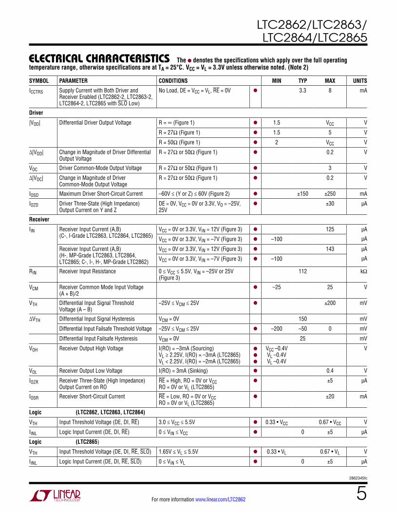
elecTrical characTerisTics
SYMBOL PARAMETER CONDITIONS MIN TYP MAX UNITS
Supplies
VCC Primary Power Supply l 3 5.5 V
VL Logic Interface Power Supply LTC2865 Only l 1.65 VCC V
ICCS Supply Current in Shutdown Mode (C-, I-Grade) (N/A LTC2863)
DE = 0V, RE = VCC = VL l 0 5 µA
Supply Current in Shutdown Mode (H-, MP-Grade) (N/A LTC2863)
DE = 0V, RE = VCC = VL l 0 40 µA
ICCTR Supply Current with Both Driver and Receiver Enabled (LTC2862-1, LTC2863-1, LTC2864-1, LTC2865 with SLO High)
No Load, DE = VCC = VL, RE = 0V l 900 1300 µA
The l denotes the specifications which apply over the full operating temperature range, otherwise specifications are at TA = 25°C. VCC = VL = 3.3V unless otherwise noted. (Note 2)
LTC2862/LTC2863/LTC2864/LTC2865
52862345fc
For more information www.linear.com/LTC2862
SYMBOL PARAMETER CONDITIONS MIN TYP MAX UNITS
ICCTRS Supply Current with Both Driver and Receiver Enabled (LTC2862-2, LTC2863-2, LTC2864-2, LTC2865 with SLO Low)
No Load, DE = VCC = VL, RE = 0V l 3.3 8 mA
Driver
|VOD| Differential Driver Output Voltage R = ∞ (Figure 1) l 1.5 VCC V
R = 27Ω (Figure 1) l 1.5 5 V
R = 50Ω (Figure 1) l 2 VCC V
Δ|VOD| Change in Magnitude of Driver Differential Output Voltage
R = 27Ω or 50Ω (Figure 1) l 0.2 V
VOC Driver Common-Mode Output Voltage R = 27Ω or 50Ω (Figure 1) l 3 V
Δ|VOC| Change in Magnitude of Driver Common-Mode Output Voltage
R = 27Ω or 50Ω (Figure 1) l 0.2 V
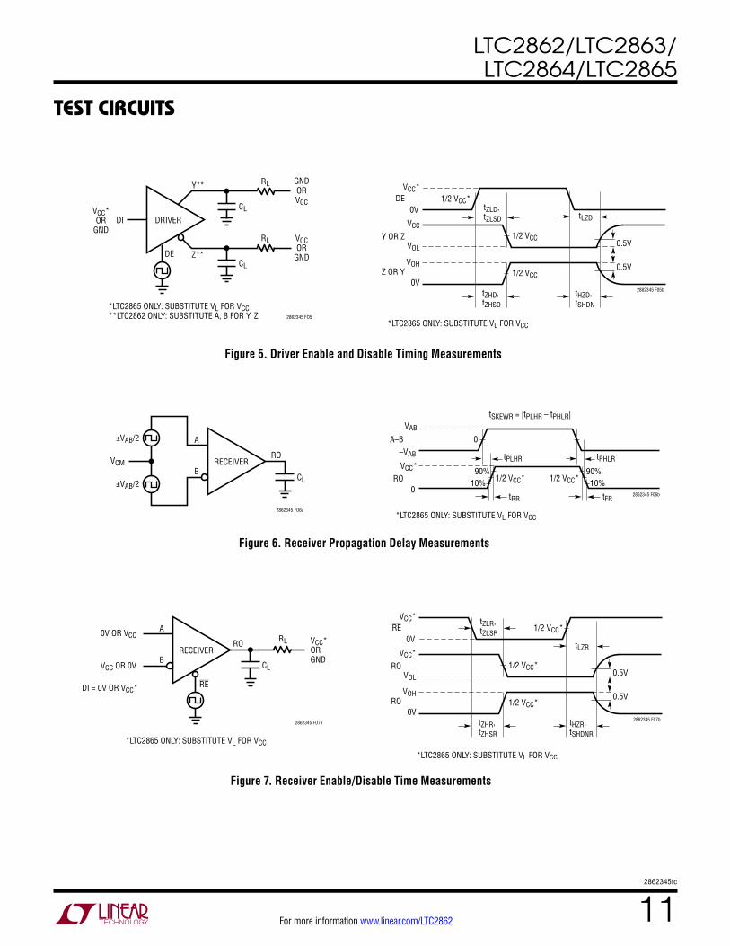
IOSD Maximum Driver Short-Circuit Current –60V ≤ (Y or Z) ≤ 60V (Figure 2) l ±150 ±250 mA
IOZD Driver Three-State (High Impedance) Output Current on Y and Z
DE = 0V, VCC = 0V or 3.3V, VO = –25V, 25V
l ±30 µA
Receiver
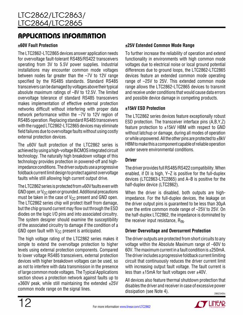
IIN Receiver Input Current (A,B) (C-, I-Grade LTC2863, LTC2864, LTC2865)
VCC = 0V or 3.3V, VIN = 12V (Figure 3) l 125 µA
µAVCC = 0V or 3.3V, VIN = –7V (Figure 3) l –100
Receiver Input Current (A,B) (H-, MP-Grade LTC2863, LTC2864, LTC2865; C-, I-, H-, MP-Grade LTC2862)
VCC = 0V or 3.3V, VIN = 12V (Figure 3) l 143 µA
µAVCC = 0V or 3.3V, VIN = –7V (Figure 3) l –100
RIN Receiver Input Resistance 0 ≤ VCC ≤ 5.5V, VIN = –25V or 25V (Figure 3)
112 kΩ
VCM Receiver Common Mode Input Voltage (A + B)/2
l –25 25 V
VTH Differential Input Signal Threshold Voltage (A – B)
–25V ≤ VCM ≤ 25V l ±200 mV
ΔVTH Differential Input Signal Hysteresis VCM = 0V 150 mV
Differential Input Failsafe Threshold Voltage –25V ≤ VCM ≤ 25V l –200 –50 0 mV
Differential Input Failsafe Hysteresis VCM = 0V 25 mV
VOH Receiver Output High Voltage I(RO) = –3mA (Sourcing) VL ≥ 2.25V, I(RO) = –3mA (LTC2865) VL < 2.25V, I(RO) = –2mA (LTC2865)
l l l
VCC –0.4V VL –0.4V VL –0.4V
V
VOL Receiver Output Low Voltage I(RO) = 3mA (Sinking) l 0.4 V
IOZR Receiver Three-State (High Impedance) Output Current on RO
RE = High, RO = 0V or VCC RO = 0V or VL (LTC2865)
l ±5 µA
IOSR Receiver Short-Circuit Current RE = Low, RO = 0V or VCC RO = 0V or VL (LTC2865)
l ±20 mA
Logic (LTC2862, LTC2863, LTC2864)
VTH Input Threshold Voltage (DE, DI, RE) 3.0 ≤ VCC ≤ 5.5V l 0.33 • VCC 0.67 • VCC V
IINL Logic Input Current (DE, DI, RE) 0 ≤ VIN ≤ VCC l 0 ±5 µA
Logic (LTC2865)
VTH Input Threshold Voltage (DE, DI, RE, SLO) 1.65V ≤ VL ≤ 5.5V l 0.33 • VL 0.67 • VL V
IINL Logic Input Current (DE, DI, RE, SLO) 0 ≤ VIN ≤ VL l 0 ±5 µA
elecTrical characTerisTics The l denotes the specifications which apply over the full operating temperature range, otherwise specifications are at TA = 25°C. VCC = VL = 3.3V unless otherwise noted. (Note 2)

LTC2862/LTC2863/LTC2864/LTC2865
62862345fc
For more information www.linear.com/LTC2862
SYMBOL PARAMETER CONDITIONS MIN TYP MAX UNITS
Driver – High Speed (LTC2862-1, LTC2863-1, LTC2864-1, LTC2865 with SLO High)
fMAX Maximum Data Rate (Note 3) l 20 Mbps
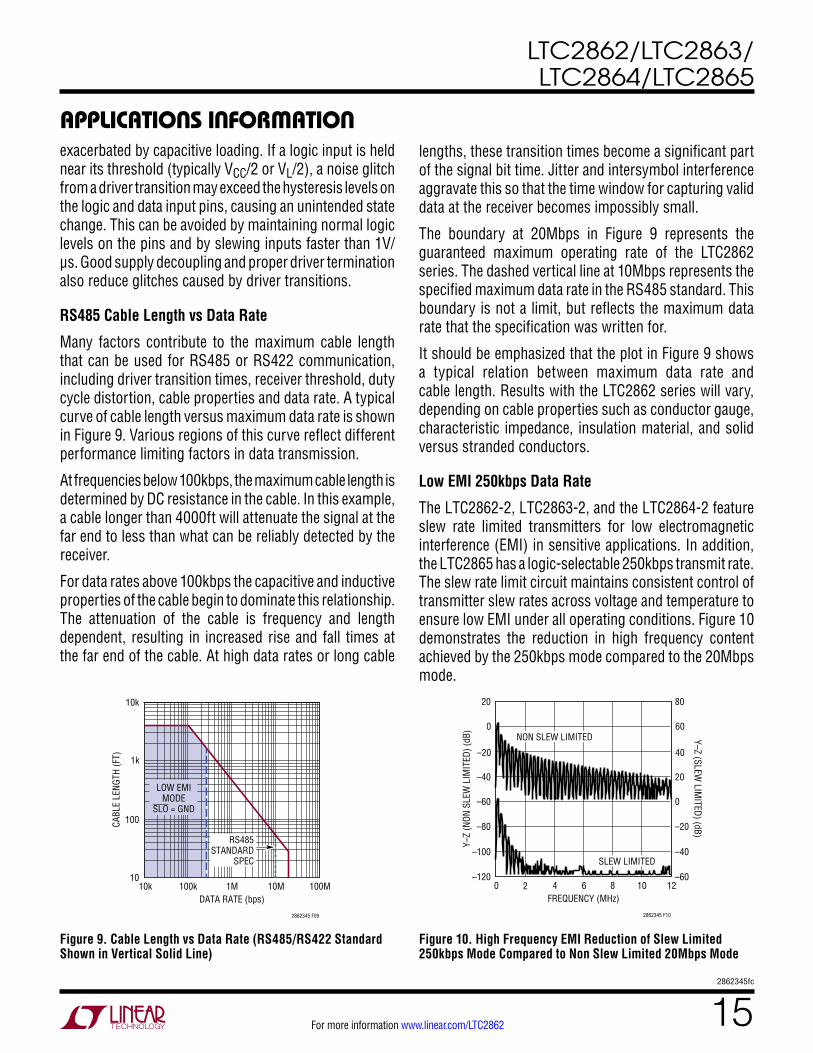
tPLHD, tPHLD Driver Input to Output RDIFF = 54Ω, CL = 100pF (Figure 4) l 25 50 ns
ΔtPD Driver Input to Output Difference |tPLHD – tPHLD|
RDIFF = 54Ω, CL = 100pF (Figure 4) l 2 9 ns
tSKEWD Driver Output Y to Output Z RDIFF = 54Ω, CL = 100pF (Figure 4) l ±10 ns
tRD, tFD Driver Rise or Fall Time RDIFF = 54Ω, CL = 100pF (Figure 4) l 4 15 ns
tZLD, tZHD, tLZD, tHZD
Driver Enable or Disable Time RL = 500Ω, CL = 50pF, RE = 0V (Figure 5)
l 180 ns
tZHSD, tZLSD Driver Enable from Shutdown RL =500Ω, CL = 50pF, RE = High (Figure 5)
l 9 µs
tSHDND Time to Shutdown RL = 500Ω, CL = 50pF, RE = High (Figure 5)
l 180 ns
Driver – Slew Rate Limited ( LTC2862-2, LTC2863-2, LTC2864-2, LTC2865 with SLO Low)
fMAX Maximum Data Rate (Note 3) l 250 kbps
tPLHD, tPHLD Driver Input to Output RDIFF = 54Ω, CL = 100pF (Figure 4) l 850 1500 ns
ΔtPD Driver Input to Output Difference |tPLHD – tPHLD|
RDIFF = 54Ω, CL = 100pF (Figure 4) l 50 500 ns
tSKEWD Driver Output Y to Output Z RDIFF = 54Ω, CL = 100pF (Figure 4) l ±500 ns
tRD, tFD Driver Rise or Fall Time RDIFF = 54Ω, CL =100pF (Figure 4) l 500 800 1200 ns
tZLD, tZHD Driver Enable Time RL = 500Ω, CL = 50pF, RE = 0V (Figure 5)
l 1200 ns
tLZD, tHZD Driver Disable Time RL = 500Ω, CL = 50pF, RE = 0V (Figure 5)
l 180 ns
tZHSD, tZLSD Driver Enable from Shutdown RL = 500Ω, CL = 50pF, RE = High (Figure 5)
l 10 µs
tSHDND Time to Shutdown RL =500Ω, CL = 50pF, RE = High (Figure 5)
l 180 ns
Receiver
tPLHR, tPHLR Receiver Input to Output CL = 15pF, VCM = 1.5V, |VAB| = 1.5V, tR and tF < 4ns (Figure 6)
l 50 65 ns
tSKEWR Differential Receiver Skew |tPLHR – tPHLR|
CL = 15pF (Figure 6) 2 9 ns
tRR, tFR Receiver Output Rise or Fall Time CL = 15pF (Figure 6) l 3 12.5 ns
tZLR, tZHR, tLZR, tHZR
Receiver Enable/Disable Time RL = 1k, CL = 15pF, DE = High (Figure 7) l 40 ns
tZHSR, tZLSR Receiver Enable from Shutdown RL = 1k, CL = 15pF, DE = 0V, (Figure 7) l 9 µs
tSHDNR Time to Shutdown RL = 1k, CL = 15pF, DE = 0V, (Figure 7) l 100 ns
swiTchinG characTerisTics The l denotes the specifications which apply over the full operating temperature range, otherwise specifications are at TA = 25°C. VCC = VL = 3.3V unless otherwise noted. (Note 2)
Note 1. Stresses beyond those listed under Absolute Maximum Ratings may cause permanent damage to the device. Exposure to any Absolute Maximum Rating condition for extended periods may affect device reliability and lifetime.Note 2. All currents into device pins are positive; all currents out of device pins are negative. All voltages are referenced to device ground unless otherwise specified.
Note 3. Maximum data rate is guaranteed by other measured parameters and is not tested directly.Note 4. This IC includes overtemperature protection that is intended to protect the device during momentary overload conditions. Junction temperature will exceed 150ºC when overtemperature protection is active. Continuous operation above the specified maximum operating temperature may result in device degradation or failure.
LTC2862/LTC2863/LTC2864/LTC2865
72862345fc
For more information www.linear.com/LTC2862
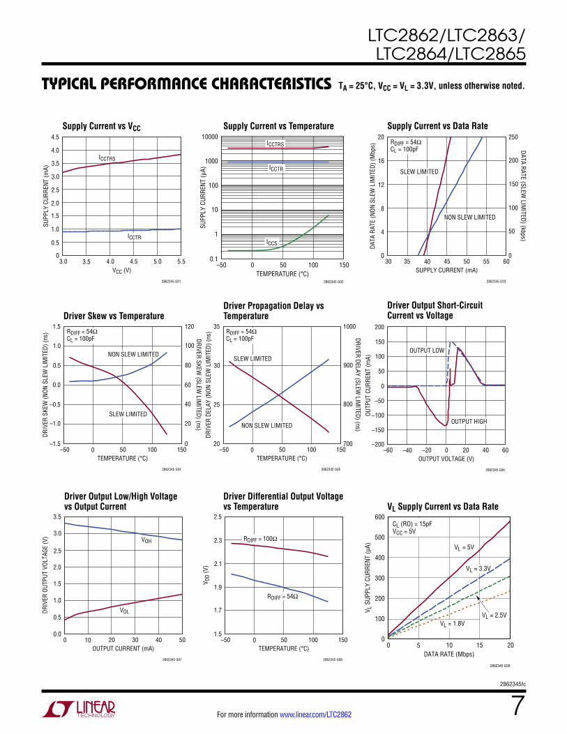
Typical perForMance characTerisTics
Driver Output Short-Circuit Current vs Voltage
Driver Output Low/High Voltage vs Output Current
Driver Differential Output Voltage vs Temperature
Supply Current vs Data Rate
Driver Skew vs TemperatureDriver Propagation Delay vs Temperature
TA = 25°C, VCC = VL = 3.3V, unless otherwise noted.
Supply Current vs TemperatureSupply Current vs VCC
OUTPUT CURRENT (mA)0
0.0
DRIV
ER O
UTPU
T VO
LTAG
E (V
)
2.0
1.5
1.0
0.5
2.5
3.0
3.5
10 20 30 40
2862345 G07
50
VOH
VOL
TEMPERATURE (°C)–50
1.5
V OD
(V)
1.9
1.7
2.1
2.3
2.5
0 50 100
2862345 G08
150
RDIFF = 100Ω
RDIFF = 54Ω
TEMPERATURE (°C)
DRIVER SKEW (SLEW
LIMITED) (ns)
–50–1.5
DRIV
ER S
KEW
(NON
SLE
W L
IMIT
ED) (
ns)
0.0
–0.5
–1.0
0.5
1.0
1.5
0 50 100
2862345 G04
1500
60
40
20
100
80
120
SLEW LIMITED
NON SLEW LIMITED
RDIFF = 54ΩCL = 100pF
TEMPERATURE (°C)
DRIVER DELAY (SLEW LIM
ITED) (ns)
–5020
DRIV
ER D
ELAY
(NON
SLE
W L
IMIT
ED) (
ns)
25
30
35
0 50 100
2862345 G05
150700
800
900
1000
SLEW LIMITED
NON SLEW LIMITED
RDIFF = 54ΩCL = 100pF
VCC (V)3.0
0
SUPP
LY C
URRE
NT (m
A)
2.0
1.5
1.0
0.5
2.5
3.0
3.5
4.5
3.5 4.0 4.5 5.0
2862345 G01
5.5
4.0ICCTRS
ICCTR
SUPPLY CURRENT (mA)
DATA RATE (SLEW LIM
ITED) (kbps)
30 350
DATA
RAT
E (N
ON S
LEW
LIM
ITED
) (M
bps)
8
4
12
16
20
40 45 50 55
2862345 G03
600
100
50
200
150
250
SLEW LIMITED
NON SLEW LIMITED
RDIFF = 54ΩCL = 100pF
OUTPUT VOLTAGE (V)–60
–200
OUTP
UT C
URRE
NT (m
A)
0
–50
–100
–150
150
100
50
200
–40 0–20 20 40
2862345 G06
60
OUTPUT LOW
OUTPUT HIGH
TEMPERATURE (°C)–50
0.1
SUPP
LY C
URRE
NT (µ
A)10
1
100
10000
0 50 100
2862345 G02
150
1000ICCTR
ICCS
ICCTRS
VL Supply Current vs Data Rate
DATA RATE (Mbps)0
0
V L S
UPPL
Y CU
RREN
T (µ
A)
200
100
300
400
500
600
5 10 15
2862345 G09
20
CL (RO) = 15pFVCC = 5V
VL = 5V
VL = 2.5V
VL = 3.3V
VL = 1.8V
LTC2862/LTC2863/LTC2864/LTC2865
82862345fc
For more information www.linear.com/LTC2862
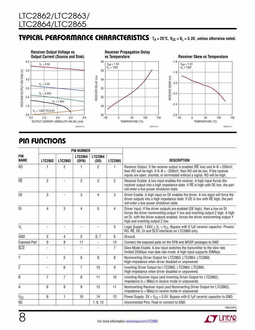
pin FuncTions
PIN NAME
PIN NUMBER
DESCRIPTION
LTC2862
LTC2863LTC2864
(DFN)LTC2864
(SO)
LTC2865
RO 1 2 1 2 1 Receiver Output. If the receiver output is enabled (RE low) and A–B > 200mV, then RO will be high. If A–B < –200mV, then RO will be low. If the receiver inputs are open, shorted, or terminated without a signal, RO will be high.
RE 2 - 2 3 2 Receiver Enable. A low input enables the receiver. A high input forces the receiver output into a high impedance state. If RE is high with DE low, the part will enter a low power shutdown state.
DE 3 - 3 4 3 Driver Enable. A high input on DE enables the driver. A low input will force the driver outputs into a high impedance state. If DE is low with RE high, the part will enter a low power shutdown state.
DI 4 3 4 5 4 Driver Input. If the driver outputs are enabled (DE high), then a low on DI forces the driver noninverting output Y low and inverting output Z high. A high on DI, with the driver outputs enabled, forces the driver noninverting output Y high and inverting output Z low.
VL - - - - 5 Logic Supply: 1.65V ≤ VL ≤ VCC. Bypass with 0.1µF ceramic capacitor. Powers RO, RE, DE, DI and SLO interfaces on LTC2865 only.
GND 5 4 5 6, 7 6 Ground.Exposed Pad 9 9 11 - 13 Connect the exposed pads on the DFN and MSOP packages to GNDSLO - - - - 7 Slow Mode Enable. A low input switches the transmitter to the slew rate
limited 250kbps max data rate mode. A high input supports 20Mbps.Y - 5 6 9 8 Noninverting Driver Output for LTC2863, LTC2864, LTC2865.
High-impedance when driver disabled or unpowered. Z - 6 7 10 9 Inverting Driver Output for LTC2863, LTC2864, LTC2865.
High-impedance when driver disabled or unpowered.B 7 7 8 11 10 Inverting Receiver Input (and Inverting Driver Output for LTC2862).
Impedance is > 96kΩ in receive mode or unpowered.A 6 8 9 12 11 Noninverting Receiver Input (and Noninverting Driver Output for LTC2862).
Impedance is > 96kΩ in receive mode or unpowered.VCC 8 1 10 14 12 Power Supply. 3V < VCC < 5.5V. Bypass with 0.1µF ceramic capacitor to GND.NC 1, 8, 13 Unconnected Pins. Float or connect to GND.
Receiver Output Voltage vs Output Current (Source and Sink)
Receiver Propagation Delay vs Temperature Receiver Skew vs Temperature
Typical perForMance characTerisTics TA = 25°C, VCC = VL = 3.3V, unless otherwise noted.
OUTPUT CURRENT (ABSOLUTE VALUE) (mA)0.0
0.0
RECE
IVER
OUT
PUT
VOLT
AGE
(V)
3.0
2.0
1.0
4.0
5.0
6.0
2.0 4.0 6.0
2862345 G10
8.0
VL = 5.5V
VL = 3.3V
VL = 2.25V
VL = 1.65V
VL = 1.65V TO 5.5V
TEMPERATURE (°C)–50
46
RECE
IVER
DEL
AY (n
s)
52
50
48
54
56
58
0 50 100
2862345 G11
150
VAB = 1.5VCL = 15pF
TEMPERATURE (°C)–50
–2.6
RECE
IVER
SKE
W (n
s)
–2.2
–2.4
–2.0
–1.8
–1.6
0 50 100
2862345 G12
150
VAB = 1.5VCL = 15pF

LTC2862/LTC2863/LTC2864/LTC2865
92862345fc
For more information www.linear.com/LTC2862
block DiaGraMs
DRIVER
MODE CONTROLLOGIC
RECEIVER
2862345 BDa
GND
*15kV ESD
DI
DE
RE
RO
VCC
A*
B*
DRIVER
RECEIVER
2862345 BDb
GND
DI
RO
VCC
A*
B*
Z*
Y*
*15kV ESD
DRIVER
MODE CONTROLLOGIC
RECEIVER
2862345 BDc
GND
DI
DE
RE
RO
VCC
A*
B*
Z*
Y*
*15kV ESD
DRIVER
MODE CONTROLLOGIC
RECEIVER
2862345 BDd
GND
*15kV ESD
DI
SLO
DE
RE
RO
VCC
A*
B*
Z*
Y*
VL
LTC2862
LTC2864 LTC2865
LTC2863
LTC2862LOGIC INPUTS MODE A, B RODE RE0 0 Receive RIN Active0 1 Shutdown RIN High-Z1 0 Transceive Active Active1 1 Transmit Active High-Z
LTC2864, LTC2865:LOGIC INPUTS MODE A, B Y, Z RODE RE0 0 Receive RIN High-Z Active0 1 Shutdown RIN High-Z High-Z1 0 Transceive RIN Active Active1 1 Transmit RIN Active High-Z
FuncTion Tables
LTC2862/LTC2863/LTC2864/LTC2865
102862345fc
For more information www.linear.com/LTC2862
TesT circuiTs
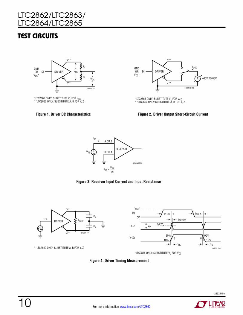
DRIVERDIGNDOR
VCC*
R
Y**
Z**
R
2862345 FO1
VOD+
–
VOC+
–
*LTC2865 ONLY: SUBSTITUTE VL FOR VCC**LTC2862 ONLY: SUBSTITUTE A, B FOR Y, Z
DRIVERDIGNDOR
VCC*
*LTC2865 ONLY: SUBSTITUTE VL FOR VCC**LTC2862 ONLY: SUBSTITUTE A, B FOR Y, Z
Y**
Z**
–60V TO 60V
2862345 FO2
IOSD
+–
RECEIVERB OR A
A OR B
VIN
IIN
2862345 FO3
+–
VINRIN = IIN
DRIVERDI
CL
CL
Y**
RDIFF
Z** 2862345 FO4
**LTC2862 ONLY: SUBSTITUTE A, B FOR Y, Z
tSKEWD
1/2 VO
tPLHD
VCC*
0VDI
Y, Z
(Y–Z)
tRD
90% 90%
2862345 F04b
10% 10%0 0
tFD
tPHLD
VO
*LTC2865 ONLY: SUBSTITUTE VL FOR VCC
Figure 1. Driver DC Characteristics Figure 2. Driver Output Short-Circuit Current
Figure 3. Receiver Input Current and Input Resistance
Figure 4. Driver Timing Measurement
LTC2862/LTC2863/LTC2864/LTC2865
112862345fc
For more information www.linear.com/LTC2862
TesT circuiTs
DRIVER
CL
RL
RL
Y**
DE Z**
2862345 FO5
CL
DIVCC*OR
GND
GNDORVCC
VCCOR
GND
*LTC2865 ONLY: SUBSTITUTE VL FOR VCC**LTC2862 ONLY: SUBSTITUTE A, B FOR Y, Z
tZLD,tZLSD
tZHD,tZHSD
tHZD,tSHDN
VCC*1/2 VCC*
VCC
VOL
VOH
0V
0VDE
Y OR Z
Z OR Y
2862345 F05b
tLZD
1/2 VCC0.5V
0.5V1/2 VCC
*LTC2865 ONLY: SUBSTITUTE VL FOR VCC
RECEIVER
CL
ROVCM
±VAB/2
±VAB/2 A
B
2862345 FO6a
tPLHR tPHLR
VAB
VCC*
–VAB
A–B
RO0
tRR tFR
90% 90%
2862345 F06b
10% 10%
0
1/2 VCC* 1/2 VCC*
*LTC2865 ONLY: SUBSTITUTE VL FOR VCC
tSKEWR = |tPLHR – tPHLR|
RECEIVER
CL
RLRO
RE
A
B
2862345 FO7a
0V OR VCC
DI = 0V OR VCC*
VCC OR 0V
VCC*ORGND
*LTC2865 ONLY: SUBSTITUTE VL FOR VCC
tZLR,tZLSR
tZHR,tZHSR
tHZR,tSHDNR
VCC*
VCC*
VOL
VOH
0V
0VRE
RO
RO
2862345 F07b
tLZR
1/2 VCC*0.5V
0.5V1/2 VCC*
*LTC2865 ONLY: SUBSTITUTE VL FOR VCC
1/2 VCC*
Figure 5. Driver Enable and Disable Timing Measurements
Figure 6. Receiver Propagation Delay Measurements
Figure 7. Receiver Enable/Disable Time Measurements
LTC2862/LTC2863/LTC2864/LTC2865
122862345fc
For more information www.linear.com/LTC2862
applicaTions inForMaTion±60V Fault Protection
The LTC2862-LTC2865 devices answer application needs for overvoltage fault-tolerant RS485/RS422 transceivers operating from 3V to 5.5V power supplies. Industrial installations may encounter common mode voltages between nodes far greater than the –7V to 12V range specified by the RS485 standards. Standard RS485 transceivers can be damaged by voltages above their typical absolute maximum ratings of –8V to 12.5V. The limited overvoltage tolerance of standard RS485 transceivers makes implementation of effective external protection networks difficult without interfering with proper data network performance within the –7V to 12V region of RS485 operation. Replacing standard RS485 transceivers with the rugged LTC2862-LTC2865 devices may eliminate field failures due to overvoltage faults without using costly external protection devices.
The ±60V fault protection of the LTC2862 series is achieved by using a high-voltage BiCMOS integrated circuit technology. The naturally high breakdown voltage of this technology provides protection in powered-off and high-impedance conditions. The driver outputs use a progressive foldback current limit design to protect against overvoltage faults while still allowing high current output drive.
The LTC2862 series is protected from ±60V faults even with GND open, or VCC open or grounded. Additional precautions must be taken in the case of VCC present and GND open. The LTC2862 series chip will protect itself from damage, but the chip ground current may flow out through the ESD diodes on the logic I/O pins and into associated circuitry. The system designer should examine the susceptibility of the associated circuitry to damage if the condition of a GND open fault with VCC present is anticipated.
The high voltage rating of the LTC2862 series makes it simple to extend the overvoltage protection to higher levels using external protection components. Compared to lower voltage RS485 transceivers, external protection devices with higher breakdown voltages can be used, so as not to interfere with data transmission in the presence of large common mode voltages. The Typical Applications section shows a protection network against faults up to ±360V peak, while still maintaining the extended ±25V common mode range on the signal lines.
±25V Extended Common Mode Range
To further increase the reliability of operation and extend functionality in environments with high common mode voltages due to electrical noise or local ground potential differences due to ground loops, the LTC2862-LTC2865 devices feature an extended common mode operating range of –25V to 25V. This extended common mode range allows the LTC2862-LTC2865 devices to transmit and receive under conditions that would cause data errors and possible device damage in competing products.
±15kV ESD Protection
The LTC2862 series devices feature exceptionally robust ESD protection. The transceiver interface pins (A,B,Y,Z) feature protection to ±15kV HBM with respect to GND without latchup or damage, during all modes of operation or while unpowered. All the other pins are protected to ±8kV HBM to make this a component capable of reliable operation under severe environmental conditions.
Driver
The driver provides full RS485/RS422 compatibility. When enabled, if DI is high, Y–Z is positive for the full-duplex devices (LTC2863-LTC2865) and A–B is positive for the half-duplex device (LTC2862).
When the driver is disabled, both outputs are high- impedance. For the full-duplex devices, the leakage on the driver output pins is guaranteed to be less than 30µA over the entire common mode range of –25V to 25V. On the half-duplex LTC2862, the impedance is dominated by the receiver input resistance, RIN.
Driver Overvoltage and Overcurrent Protection
The driver outputs are protected from short circuits to any voltage within the Absolute Maximum range of –60V to 60V. The maximum current in a fault condition is ±250mA. The driver includes a progressive foldback current limiting circuit that continuously reduces the driver current limit with increasing output fault voltage. The fault current is less than ±15mA for fault voltages over ±40V.
All devices also feature thermal shutdown protection that disables the driver and receiver in case of excessive power dissipation (see Note 4).

LTC2862/LTC2863/LTC2864/LTC2865
132862345fc
For more information www.linear.com/LTC2862
applicaTions inForMaTionFull Failsafe Operation
When the absolute value of the differential voltage between the A and B pins is greater than 200mV with the receiver enabled, the state of RO will reflect the polarity of (A–B).
These parts have a failsafe feature that guarantees the receiver output will be in a logic 1 state (the idle state) when the inputs are shorted, left open, or terminated but not driven, for more than about 3µs. The delay allows normal data signals to transition through the threshold region without being interpreted as a failsafe condition. This failsafe feature is guaranteed to work for inputs spanning the entire common mode range of –25V to 25V.
Most competing devices achieve the failsafe function by a simple negative offset of the input threshold voltage. This causes the receiver to interpret a zero differential voltage as a logic 1 state. The disadvantage of this approach is the input offset can introduce duty cycle asymmetry at the receiver output that becomes increasingly worse with low input signal levels and slow input edge rates.
Other competing devices use internal biasing resistors to create a positive bias at the receiver inputs in the absence of an external signal. This type of failsafe biasing is ineffective if the network lines are shorted, or if the network is terminated but not driven by an active transmitter.
the positive and negative thresholds. If this condition persists for more than about 3µs the failsafe condition is asserted and the RO pin is forced to the logic 1 state. This circuit provides full failsafe operation with no negative impact to receiver duty cycle symmetry, as shown in Figure 8. The input signal in Figure 8 was obtained by driving a 10Mbps RS485 signal through 1000 feet of cable, thereby attenuating it to a ±200mV signal with slow rise and fall times. Good duty cycle symmetry is observed at RO despite the degraded input signal.
Enhanced Receiver Noise Immunity
An additional benefit of the fully symmetric receiver thresholds is enhanced receiver noise immunity. The differential input signal must go above the positive threshold to register as a logic 1 and go below the negative threshold to register as a logic 0. This provides a hysteresis of 150mV (typical) at the receiver inputs for any valid data signal. (An invalid data condition such as a DC sweep of the receiver inputs will produce a different observed hysteresis due to the activation of the failsafe circuit.) Competing devices that employ a negative offset of the input threshold voltage generally have a much smaller hysteresis and subsequently have lower receiver noise immunity.
RS485 Network Biasing
RS485 networks are usually biased with a resistive divider to generate a differential voltage of ≥200mV on the data lines, which establishes a logic 1 state (the idle state) when all the transmitters on the network are disabled. The values of the biasing resistors are not fixed, but depend on the number and type of transceivers on the line and the number and value of terminating resistors. Therefore, the values of the biasing resistors must be customized to each specific network installation, and may change if nodes are added to or removed from the network.
The internal failsafe feature of the LTC2862-LTC2865 eliminates the need for external network biasing resistors provided they are used in a network of transceivers with similar internal failsafe features. The LTC2862-LTC2865 transceivers will operate correctly on biased, unbiased, or under-biased networks.
Figure 8. Duty Cycle of Balanced Receiver with ±200mV 10Mbps Input Signal
A, B200mV/DIV
A–B200mV/DIV
40ns/DIV 2862345 F08
RO1.6V/DIV
The LTC2862 series uses fully symmetric positive and negative receiver thresholds (typically ±75mV) to maintain good duty cycle symmetry at low signal levels. The failsafe operation is performed with a window comparator to determine when the differential input voltage falls between

LTC2862/LTC2863/LTC2864/LTC2865
142862345fc
For more information www.linear.com/LTC2862
Hi-Z State
The receiver output is internally driven high (to VCC or VL) or low (to GND) with no external pull-up needed. When the receiver is disabled the RO pin becomes Hi-Z with leakage of less than ±5μA for voltages within the supply range.
High Receiver Input Resistance
The receiver input load from A or B to GND for the LTC2863, LTC2864, and LTC2865 is less than one-eighth unit load, permitting a total of 256 receivers per system without exceeding the RS485 receiver loading specification. All grades of the LTC2862 and the H- and MP-grade devices of the LTC2863, LTC2864, and LTC2865 have an input load less than one-seventh unit load over the complete temperature range of –40°C to 125°C. The increased input load specification for these devices is due to increased junction leakage at high temperature and the transmitter circuitry sharing the A and B pins on the LTC2862. The input load of the receiver is unaffected by enabling/disabling the receiver or by powering/unpowering the part.
Supply CurrentThe unloaded static supply currents in these devices are low —typically 900μA for non slew limited devices and 3.3mA for slew limited devices. In applications with resistively terminated cables, the supply current is dominated by the driver load. For example, when using two 120Ω terminators with a differential driver output voltage of 2V, the DC load current is 33mA, which is sourced by the positive voltage supply. Power supply current increases with toggling data due to capacitive loading and this term can increase significantly at high data rates. A plot of the supply current vs data rate is shown in the Typical Performance Characteristics of this data sheet.
During fault conditions with a positive voltage larger than the supply voltage applied to the transmitter pins, or during transmitter operation with a high positive common mode voltage, positive current of up to 80mA may flow from the transmitter pins back to VCC. If the system power supply or loading cannot sink this excess current, a 5.6V 1W 1N4734 Zener diode may be placed between VCC and GND to prevent an overvoltage condition on VCC.
There are no power-up sequence restrictions on the LTC2865. However, correct operation is not guaranteed for VL > VCC.
Shutdown Mode Delay
The LTC2862, LTC2864, and LTC2865 feature a low power shutdown mode that is entered when both the driver and the receiver are simultaneously disabled (pin DE low and RE high). A shutdown mode delay of approximately 250ns (not tested in production) is imposed after this state is received before the chip enters shutdown. If either DE goes high or RE goes low during this delay, the delay timer is reset and the chip does not enter shutdown. This reduces the chance of accidentally entering shutdown if DE and RE are driven in parallel by a slowly changing signal or if DE and RE are driven by two independent signals with a timing skew between them.
This shutdown mode delay does not affect the outputs of the transmitter and receiver, which start to switch to the high impedance state upon the reception of their respec-tive disable signals as defined by the parameters tSHDND and tSHDNR. The shutdown mode delay affects only the time when all the internal circuits that draw DC power from VCC are turned off.
High Speed Considerations
A ground plane layout with a 0.1µF bypass capacitor placed less than 7mm away from the VCC pin is recommended. The PC board traces connected to signals A/B and Z/Y should be symmetrical and as short as possible to maintain good differential signal integrity. To minimize capacitive effects, the differential signals should be separated by more than the width of a trace and should not be routed on top of each other if they are on different signal planes.
Care should be taken to route outputs away from any sensitive inputs to reduce feedback effects that might cause noise, jitter, or even oscillations. For example, in the full-duplex devices, DI and A/B should not be routed near the driver or receiver outputs.
The logic inputs have a typical hysteresis of 100mV to provide noise immunity. Fast edges on the outputs can cause glitches in the ground and power supplies which are
applicaTions inForMaTion
LTC2862/LTC2863/LTC2864/LTC2865
152862345fc
For more information www.linear.com/LTC2862
exacerbated by capacitive loading. If a logic input is held near its threshold (typically VCC/2 or VL/2), a noise glitch from a driver transition may exceed the hysteresis levels on the logic and data input pins, causing an unintended state change. This can be avoided by maintaining normal logic levels on the pins and by slewing inputs faster than 1V/μs. Good supply decoupling and proper driver termination also reduce glitches caused by driver transitions.
RS485 Cable Length vs Data Rate
Many factors contribute to the maximum cable length that can be used for RS485 or RS422 communication, including driver transition times, receiver threshold, duty cycle distortion, cable properties and data rate. A typical curve of cable length versus maximum data rate is shown in Figure 9. Various regions of this curve reflect different performance limiting factors in data transmission.
At frequencies below 100kbps, the maximum cable length is determined by DC resistance in the cable. In this example, a cable longer than 4000ft will attenuate the signal at the far end to less than what can be reliably detected by the receiver.
For data rates above 100kbps the capacitive and inductive properties of the cable begin to dominate this relationship. The attenuation of the cable is frequency and length dependent, resulting in increased rise and fall times at the far end of the cable. At high data rates or long cable
applicaTions inForMaTionlengths, these transition times become a significant part of the signal bit time. Jitter and intersymbol interference aggravate this so that the time window for capturing valid data at the receiver becomes impossibly small.
The boundary at 20Mbps in Figure 9 represents the guaranteed maximum operating rate of the LTC2862 series. The dashed vertical line at 10Mbps represents the specified maximum data rate in the RS485 standard. This boundary is not a limit, but reflects the maximum data rate that the specification was written for.
It should be emphasized that the plot in Figure 9 shows a typical relation between maximum data rate and cable length. Results with the LTC2862 series will vary, depending on cable properties such as conductor gauge, characteristic impedance, insulation material, and solid versus stranded conductors.
Low EMI 250kbps Data Rate
The LTC2862-2, LTC2863-2, and the LTC2864-2 feature slew rate limited transmitters for low electromagnetic interference (EMI) in sensitive applications. In addition, the LTC2865 has a logic-selectable 250kbps transmit rate. The slew rate limit circuit maintains consistent control of transmitter slew rates across voltage and temperature to ensure low EMI under all operating conditions. Figure 10 demonstrates the reduction in high frequency content achieved by the 250kbps mode compared to the 20Mbps mode.
Figure 9. Cable Length vs Data Rate (RS485/RS422 Standard Shown in Vertical Solid Line)
Figure 10. High Frequency EMI Reduction of Slew Limited 250kbps Mode Compared to Non Slew Limited 20Mbps Mode
DATA RATE (bps)10k
10
CABL
E LE
NGTH
(FT)
100
1k
10k
100k 1M 10M
2862345 F09
100M
LOW EMIMODE
SLO = GND
RS485STANDARD
SPEC
FREQUENCY (MHz)0
–120
Y–Z
(NON
SLE
W L
IMIT
ED) (
dB)
–40
–60
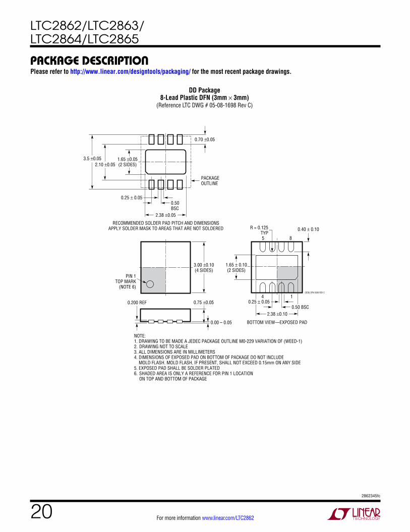
–80
–100
–20
0
20
–60
Y–Z (SLEW LIM
ITED) (dB)
20
0
–20
–40
40
60
80
2 4 6 8 10
2862345 F10
12
NON SLEW LIMITED
SLEW LIMITED

LTC2862/LTC2863/LTC2864/LTC2865
162862345fc
For more information www.linear.com/LTC2862
The 250kbps mode has the added advantage of reducing signal reflections in an unterminated network, and there-by increasing the length of a network that can be used without termination. Using the rule of thumb that the rise time of the transmitter should be greater than four times the one-way delay of the signal, networks of up to 140 feet can be driven without termination.
PROFIBUS Compatible Interface
PROFIBUS is an RS485-based field bus. In addition to the specifications of TIA/EIA-485-A, the PROFIBUS specification contains additional requirements for cables, interconnects, line termination, and signal levels. The following discussion applies to the PROFIBUS Type A cables with associated connectors and termination. The Type A cable is a twisted pair shielded cable with a characteristic impedance of 135Ω to 165Ω and a loop resistance of < 110Ω/km.
The LTC2865 family of RS485 transceivers may be used in PROFIBUS compatible equipment if the following considerations are implemented. (Please refer to the schematic of the PROFIBUS Compatible Interface in the Typical Applications Section.)
1. The polarity of the PROFIBUS signal is opposite to the polarity convention used in this data sheet. The PRO-FIBUS B wire is driven by a non-inverted signal, while the A wire is driven by an inverted signal. Therefore, it is necessary to swap the output connections from the transceiver. Pin A is connected to the PROFIBUS B wire, and Pin B is connected to the PROFIBUS A wire.
2. Each end of the PROFIBUS line is terminated with a 220Ω resistor between B and A, a 390Ω pull-up resis-tor between B and VCC, and a 390Ω pull-down resistor be-tween A and GND. This provides suitable termination for the 150Ω twisted pair transmission cable.
3. The peak to peak differential voltage VOD received at the end of a 100m cable with the cable and termina-tions described above must be greater than 4V and less than 7V. The LTC2865 family produces signal levels in excess of 7V when driving this network directly. 8.2Ω resistors may be inserted between the A and B pins of the transceiver and the B and A pins of the PROFIBUS
cable to attenuate the transmitted signal to meet the PROFIBUS upper limit of 7V while still providing enough drive strength to meet the lower limit of 4V.
4. The LTC2865 family transceiver should be powered by a 5% tolerance 5V supply (4.75V to 5.25V) to ensure that the PROFIBUS VOD tolerances are met.
Auxiliary Protection For IEC Surge, EFT and ESD
An interface transceiver used in an industrial setting may be exposed to extremely high levels of electrical overstress due to phenomena such as lightning surge, electrical fast transient (EFT) from switching high current inductive loads, and electrostatic discharge (ESD) from the discharge of electrically charged personnel or equip-ment. Test methods to evaluate immunity of electronic equipment to these phenomenon are defined in the IEC standards 61000-4-2, 61000-4-4, and 61000-4-5, which address ESD, EFT, and surge, respectively. The transi-ents produced by the EFT and particularly the surge tests contain much more energy than the ESD transients. The LTC2865 family is designed for high robustness against ESD, but the on-chip protection is not able to absorb the energy associated with the 61000-4-5 surge transients. Therefore, a properly designed external protection network is necessary to achieve a high level of surge protection, and can also extend the ESD and EFT performance of the LTC2865 family to extremely high levels.
In addition to providing surge, EFT and ESD protection, an external network should preserve or extend the ability of the LTC2865 family to withstand overvoltage faults, operate over a wide common mode, and communicate at high frequencies. In order to meet the first two requirements, protection components with suitably high conduction voltages must be chosen. A means to limit current must be provided to prevent damage in case a secondary protection device or the ESD cell on the LTC2865 family fires and conducts. The capacitance of these components must be kept low in order to permit high frequency communication over a network with multiple nodes. Meeting the requirements for conducting very high energy electrical transients while maintaining high hold-off voltages and low capacitance is a considerable challenge.
applicaTions inForMaTion

LTC2862/LTC2863/LTC2864/LTC2865
172862345fc
For more information www.linear.com/LTC2862
applicaTions inForMaTionA protection network shown in the Typical Applications section (network for IEC level 4 protection against surge, EFT and ESD) meets this challenge. The network provides the following protection:
• IEC 61000-4-2 ESD Level 4: ±30KV contact, ±30kV air (line to GND, direct discharge to bus pins with transceiver and protection circuit mounted on a ground referenced test card per Figure 4 of the standard)
• IEC 61000-4-4 EFT Level 4: ±5KV (line to GND, 5kHz repetition rate, 15ms burst duration, 60 second test duration, discharge coupled to bus pins through 100pF capacitor per paragraph 7.3.2 of the standard)
• IEC 61000-4-5 Surge Level 4: ±5KV (line to GND, line to line, 8/20µs waveform, each line coupled to generator through 80Ω resistor per Figure 14 of the standard)
This protection circuit adds only ~8pF of capacitance per line (line to GND), thereby providing an extremely high level of protection without significant impact to the performance of the LTC2865 family transceivers at high data rates.
The gas discharge tubes (GDTs) provide the primary pro-tection against electrical surges. These devices provide a very low impedance and high current carrying capability when they fire, safely discharging the surge current to GND. The transient blocking units (TBUs) are solid state devices that switch from a low impedance pass through state to a high impedance current limiting state when a specified current level is reached. These devices limit the current and power that can pass through to the secondary protection. The secondary protection consists of a bidirectional thyristor, which triggers above 35V to protect the bus pins of the LTC2865 family transceiver. The high trigger voltage of the secondary protection maintains the full ±25V common mode range of the receivers. The final component of the network is the metal oxide varistors (MOVs) which are used to clamp the voltage across the TBUs to protect them against fast ESD and EFT transients which exceed the turn-on time of the GDT.
The high performance of this network is attributable to the low capacitance of the GDT and thyristor primary and secondary protection devices. The high capacitance MOV floats on the line and is shunted by the TBU, so it contributes no appreciable capacitive load on the signal.
PROFIBUS Compatible Line Interface
Typical applicaTions
RO
RE
DE
DI
8.2Ω
2862345 TA02
A*
B*
* THE POLARITY OF A AND B IN THIS DATA SHEET IS OPPOSITE THE POLARITY DEFINED BY PROFIBUS.
VCC(4.75V TO 5.25V)
GND
LTC2862-1
8.2Ω
390Ω
4VP-P ≤ VOD ≤ 7VP-P AT 12Mbps
220Ω
390Ω
B WIRE
A WIRE
B WIRE
A WIRE
VCC
390Ω
220Ω
390Ω
VCC
100m
5.5Ω/WIRE
VOD

LTC2862/LTC2863/LTC2864/LTC2865
182862345fc
For more information www.linear.com/LTC2862
Typical applicaTions
RO
DE
DI
R
D
RO
DE
DI/
VCCB
A
GND
2862345 TA04
“A”
“B”
5VLTC2862
I1
I2
Failsafe O Application (Idle State = Logic O)
Bidirectional ±60V 20Mbps Level Shifter/Isolator
DI
GND
VCC
VCC
RO
LTC2863-1
VCC
R1
R1
R2
R2
±60V
C
C
A
B
R1
Y
Z
DATA OUT 2
R1 = 100k 1%. PLACE R1 RESISTORS NEAR A AND B PINS.R2 = 10kC = 47pF, 5%, 50 WVDC. MAY BE OMITTED FOR DATA RATES ≤ 100kbps.
DATA IN 1 DATA OUT 1
DATA IN 2
VCC
RO
LTC2863-1
Y
Z
DI
GNDC
A
B
2862345 TA03
R1
C

LTC2862/LTC2863/LTC2864/LTC2865
192862345fc
For more information www.linear.com/LTC2862
.016 – .050(0.406 – 1.270)
.010 – .020(0.254 – 0.508)
× 45°
0°– 8° TYP.008 – .010
(0.203 – 0.254)
SO8 REV G 0212
.053 – .069(1.346 – 1.752)
.014 – .019(0.355 – 0.483)
TYP
.004 – .010(0.101 – 0.254)
.050(1.270)
BSC
1 2 3 4
.150 – .157(3.810 – 3.988)
NOTE 3
8 7 6 5
.189 – .197(4.801 – 5.004)
NOTE 3
.228 – .244(5.791 – 6.197)
.245MIN .160 ±.005
RECOMMENDED SOLDER PAD LAYOUT
.045 ±.005 .050 BSC
.030 ±.005 TYP
INCHES(MILLIMETERS)
NOTE:1. DIMENSIONS IN
2. DRAWING NOT TO SCALE3. THESE DIMENSIONS DO NOT INCLUDE MOLD FLASH OR PROTRUSIONS. MOLD FLASH OR PROTRUSIONS SHALL NOT EXCEED .006" (0.15mm)4. PIN 1 CAN BE BEVEL EDGE OR A DIMPLE
S8 Package8-Lead Plastic Small Outline (Narrow .150 Inch)
(Reference LTC DWG # 05-08-1610 Rev G)
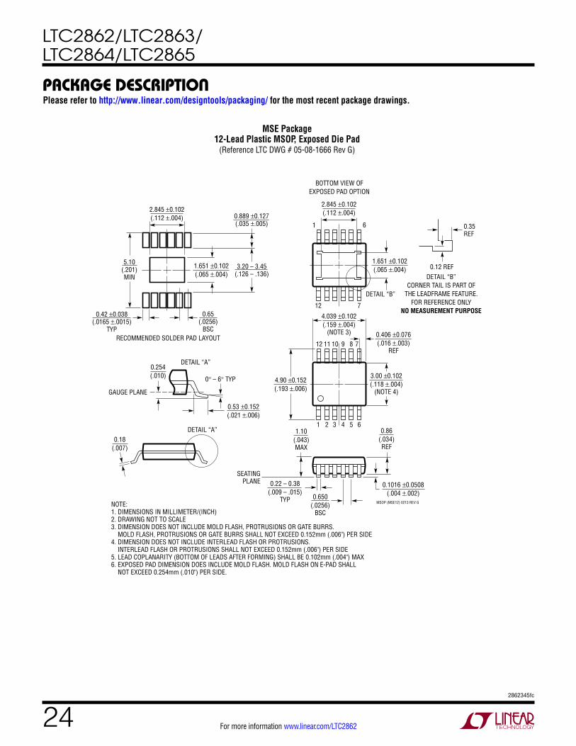
packaGe DescripTionPlease refer to http://www.linear.com/designtools/packaging/ for the most recent package drawings.
LTC2862/LTC2863/LTC2864/LTC2865
202862345fc
For more information www.linear.com/LTC2862
DD Package8-Lead Plastic DFN (3mm × 3mm)
(Reference LTC DWG # 05-08-1698 Rev C)
3.00 ±0.10(4 SIDES)
NOTE:1. DRAWING TO BE MADE A JEDEC PACKAGE OUTLINE M0-229 VARIATION OF (WEED-1)2. DRAWING NOT TO SCALE3. ALL DIMENSIONS ARE IN MILLIMETERS4. DIMENSIONS OF EXPOSED PAD ON BOTTOM OF PACKAGE DO NOT INCLUDE MOLD FLASH. MOLD FLASH, IF PRESENT, SHALL NOT EXCEED 0.15mm ON ANY SIDE5. EXPOSED PAD SHALL BE SOLDER PLATED6. SHADED AREA IS ONLY A REFERENCE FOR PIN 1 LOCATION ON TOP AND BOTTOM OF PACKAGE
0.40 ± 0.10
BOTTOM VIEW—EXPOSED PAD
1.65 ± 0.10(2 SIDES)
0.75 ±0.05
R = 0.125TYP
2.38 ±0.10
14
85
PIN 1TOP MARK
(NOTE 6)
0.200 REF
0.00 – 0.05
(DD8) DFN 0509 REV C
0.25 ± 0.05
2.38 ±0.05
RECOMMENDED SOLDER PAD PITCH AND DIMENSIONSAPPLY SOLDER MASK TO AREAS THAT ARE NOT SOLDERED
1.65 ±0.05(2 SIDES)2.10 ±0.05
0.50BSC
0.70 ±0.05
3.5 ±0.05
PACKAGEOUTLINE
0.25 ± 0.050.50 BSC
packaGe DescripTionPlease refer to http://www.linear.com/designtools/packaging/ for the most recent package drawings.
LTC2862/LTC2863/LTC2864/LTC2865
212862345fc
For more information www.linear.com/LTC2862
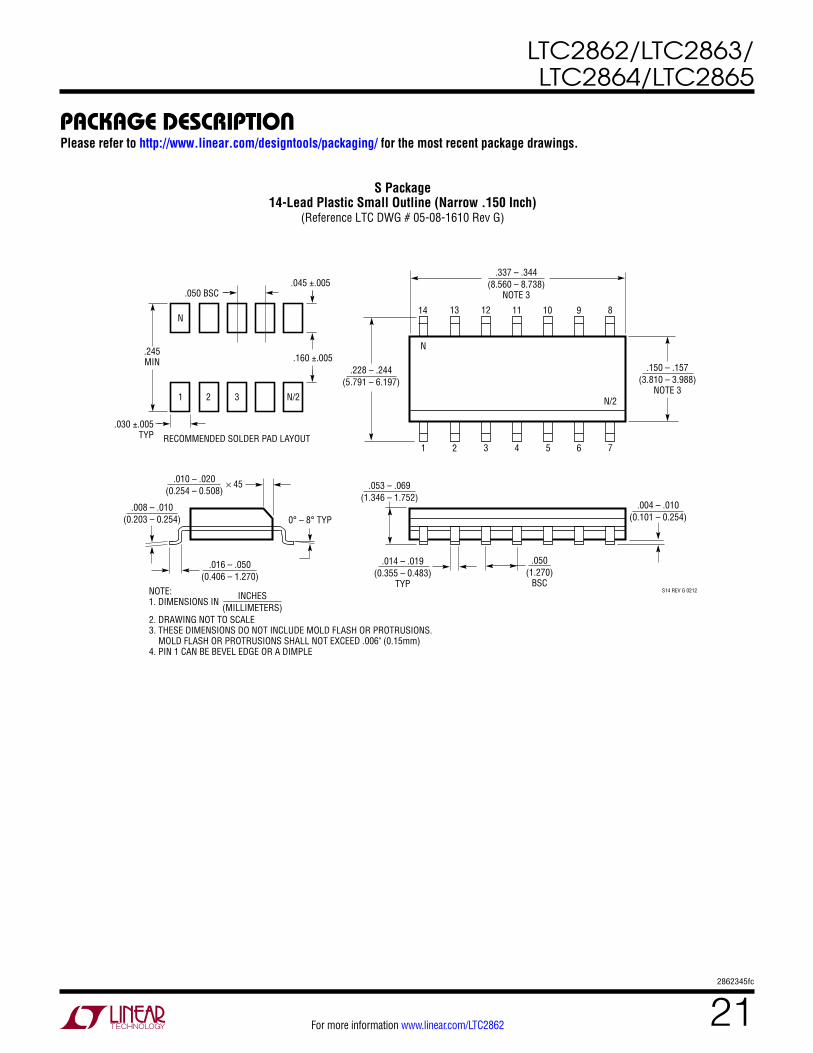
1
N
2 3 4
.150 – .157(3.810 – 3.988)
NOTE 3
14 13
.337 – .344(8.560 – 8.738)
NOTE 3
.228 – .244(5.791 – 6.197)
12 11 10 9
5 6 7
N/2
8
.016 – .050(0.406 – 1.270)
.010 – .020(0.254 – 0.508)
× 45
0° – 8° TYP.008 – .010
(0.203 – 0.254)
S14 REV G 0212
.053 – .069(1.346 – 1.752)
.014 – .019(0.355 – 0.483)
TYP
.004 – .010(0.101 – 0.254)
.050(1.270)
BSC
.245MIN
N
1 2 3 N/2
.160 ±.005
RECOMMENDED SOLDER PAD LAYOUT
.045 ±.005 .050 BSC
.030 ±.005 TYP
INCHES(MILLIMETERS)
NOTE:1. DIMENSIONS IN
2. DRAWING NOT TO SCALE3. THESE DIMENSIONS DO NOT INCLUDE MOLD FLASH OR PROTRUSIONS. MOLD FLASH OR PROTRUSIONS SHALL NOT EXCEED .006" (0.15mm)4. PIN 1 CAN BE BEVEL EDGE OR A DIMPLE
S Package14-Lead Plastic Small Outline (Narrow .150 Inch)
(Reference LTC DWG # 05-08-1610 Rev G)
packaGe DescripTionPlease refer to http://www.linear.com/designtools/packaging/ for the most recent package drawings.
LTC2862/LTC2863/LTC2864/LTC2865
222862345fc
For more information www.linear.com/LTC2862
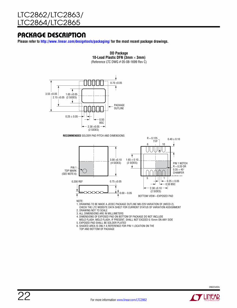
DD Package10-Lead Plastic DFN (3mm × 3mm)
(Reference LTC DWG # 05-08-1699 Rev C)
3.00 ±0.10(4 SIDES)
NOTE:1. DRAWING TO BE MADE A JEDEC PACKAGE OUTLINE M0-229 VARIATION OF (WEED-2). CHECK THE LTC WEBSITE DATA SHEET FOR CURRENT STATUS OF VARIATION ASSIGNMENT2. DRAWING NOT TO SCALE3. ALL DIMENSIONS ARE IN MILLIMETERS4. DIMENSIONS OF EXPOSED PAD ON BOTTOM OF PACKAGE DO NOT INCLUDE MOLD FLASH. MOLD FLASH, IF PRESENT, SHALL NOT EXCEED 0.15mm ON ANY SIDE5. EXPOSED PAD SHALL BE SOLDER PLATED6. SHADED AREA IS ONLY A REFERENCE FOR PIN 1 LOCATION ON THE TOP AND BOTTOM OF PACKAGE
0.40 ± 0.10
BOTTOM VIEW—EXPOSED PAD
1.65 ± 0.10(2 SIDES)
0.75 ±0.05
R = 0.125TYP
2.38 ±0.10(2 SIDES)
15
106
PIN 1TOP MARK
(SEE NOTE 6)
0.200 REF
0.00 – 0.05
(DD) DFN REV C 0310
0.25 ± 0.05
2.38 ±0.05(2 SIDES)
RECOMMENDED SOLDER PAD PITCH AND DIMENSIONS
1.65 ±0.05(2 SIDES)2.15 ±0.05
0.50BSC
0.70 ±0.05
3.55 ±0.05
PACKAGEOUTLINE
0.25 ± 0.050.50 BSC
DD Package10-Lead Plastic DFN (3mm × 3mm)
(Reference LTC DWG # 05-08-1699 Rev C)
PIN 1 NOTCHR = 0.20 OR0.35 × 45°CHAMFER
packaGe DescripTionPlease refer to http://www.linear.com/designtools/packaging/ for the most recent package drawings.
LTC2862/LTC2863/LTC2864/LTC2865
232862345fc
For more information www.linear.com/LTC2862
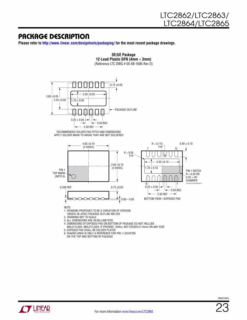
DE/UE Package12-Lead Plastic DFN (4mm × 3mm)
(Reference LTC DWG # 05-08-1695 Rev D)
4.00 ±0.10(2 SIDES)
3.00 ±0.10(2 SIDES)
NOTE:1. DRAWING PROPOSED TO BE A VARIATION OF VERSION (WGED) IN JEDEC PACKAGE OUTLINE M0-2292. DRAWING NOT TO SCALE3. ALL DIMENSIONS ARE IN MILLIMETERS4. DIMENSIONS OF EXPOSED PAD ON BOTTOM OF PACKAGE DO NOT INCLUDE MOLD FLASH. MOLD FLASH, IF PRESENT, SHALL NOT EXCEED 0.15mm ON ANY SIDE5. EXPOSED PAD SHALL BE SOLDER PLATED6. SHADED AREA IS ONLY A REFERENCE FOR PIN 1 LOCATION ON THE TOP AND BOTTOM OF PACKAGE
0.40 ± 0.10
BOTTOM VIEW—EXPOSED PAD
1.70 ± 0.10
0.75 ±0.05
R = 0.115TYP
R = 0.05TYP
2.50 REF
16
127
PIN 1 NOTCHR = 0.20 OR0.35 × 45°CHAMFER
PIN 1TOP MARK
(NOTE 6)
0.200 REF
0.00 – 0.05
(UE12/DE12) DFN 0806 REV D
2.50 REF
RECOMMENDED SOLDER PAD PITCH AND DIMENSIONSAPPLY SOLDER MASK TO AREAS THAT ARE NOT SOLDERED
2.20 ±0.05
0.70 ±0.05
3.60 ±0.05
PACKAGE OUTLINE
3.30 ±0.10
0.25 ± 0.050.50 BSC
1.70 ± 0.05
3.30 ±0.05
0.50 BSC0.25 ± 0.05
packaGe DescripTionPlease refer to http://www.linear.com/designtools/packaging/ for the most recent package drawings.
LTC2862/LTC2863/LTC2864/LTC2865
242862345fc
For more information www.linear.com/LTC2862
packaGe DescripTionPlease refer to http://www.linear.com/designtools/packaging/ for the most recent package drawings.
MSOP (MSE12) 0213 REV G
0.53 ±0.152(.021 ±.006)
SEATINGPLANE
0.18(.007)
1.10(.043)MAX
0.22 – 0.38(.009 – .015)
TYP
0.86(.034)REF
0.650(.0256)
BSC
12
12 11 10 9 8 7
7
DETAIL “B”
1 6
NOTE:1. DIMENSIONS IN MILLIMETER/(INCH)2. DRAWING NOT TO SCALE3. DIMENSION DOES NOT INCLUDE MOLD FLASH, PROTRUSIONS OR GATE BURRS. MOLD FLASH, PROTRUSIONS OR GATE BURRS SHALL NOT EXCEED 0.152mm (.006") PER SIDE4. DIMENSION DOES NOT INCLUDE INTERLEAD FLASH OR PROTRUSIONS. INTERLEAD FLASH OR PROTRUSIONS SHALL NOT EXCEED 0.152mm (.006") PER SIDE5. LEAD COPLANARITY (BOTTOM OF LEADS AFTER FORMING) SHALL BE 0.102mm (.004") MAX6. EXPOSED PAD DIMENSION DOES INCLUDE MOLD FLASH. MOLD FLASH ON E-PAD SHALL NOT EXCEED 0.254mm (.010") PER SIDE.
0.254(.010) 0° – 6° TYP
DETAIL “A”
DETAIL “A”
GAUGE PLANE
RECOMMENDED SOLDER PAD LAYOUT
BOTTOM VIEW OFEXPOSED PAD OPTION
2.845 ±0.102(.112 ±.004)2.845 ±0.102
(.112 ±.004)
4.039 ±0.102(.159 ±.004)
(NOTE 3)
1.651 ±0.102(.065 ±.004)
1.651 ±0.102(.065 ±.004)
0.1016 ±0.0508(.004 ±.002)
1 2 3 4 5 6
3.00 ±0.102(.118 ±.004)
(NOTE 4)
0.406 ±0.076(.016 ±.003)
REF
4.90 ±0.152(.193 ±.006)
DETAIL “B”CORNER TAIL IS PART OF
THE LEADFRAME FEATURE.FOR REFERENCE ONLY
NO MEASUREMENT PURPOSE
0.12 REF
0.35REF
5.10(.201)MIN
3.20 – 3.45(.126 – .136)
0.889 ±0.127(.035 ±.005)
0.42 ±0.038(.0165 ±.0015)
TYP
0.65(.0256)
BSC
MSE Package12-Lead Plastic MSOP, Exposed Die Pad
(Reference LTC DWG # 05-08-1666 Rev G)
MSE Package12-Lead Plastic MSOP, Exposed Die Pad
(Reference LTC DWG # 05-08-1666 Rev G)
LTC2862/LTC2863/LTC2864/LTC2865
252862345fc
For more information www.linear.com/LTC2862
Information furnished by Linear Technology Corporation is believed to be accurate and reliable. However, no responsibility is assumed for its use. Linear Technology Corporation makes no representa-tion that the interconnection of its circuits as described herein will not infringe on existing patent rights.
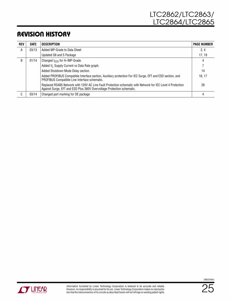
revision hisToryREV DATE DESCRIPTION PAGE NUMBER
A 03/13 Added MP-Grade to Data SheetUpdated S8 and S Package
2, 417, 19
B 01/14 Changed ICCS for H-/MP-Grade.Added VL Supply Current vs Data Rate graph.Added Shutdown Mode Delay section.Added PROFIBUS Compatible Interface section, Auxiliary protection For IEC Surge, EFT and ESD section, and PROFIBUS Compatible Line Interface schematic.Replaced RS485 Network with 120V AC Line Fault Protection schematic with Network for IEC Level 4 Protection Against Surge, EFT and ESD Plus 360V Overvoltage Protection schematic.
47
1416, 17
26
C 03/14 Changed part marking for DE package 4

LTC2862/LTC2863/LTC2864/LTC2865
262862345fc
For more information www.linear.com/LTC2862 LINEAR TECHNOLOGY CORPORATION 2011
LT 0314 REV C • PRINTED IN USALinear Technology Corporation1630 McCarthy Blvd., Milpitas, CA 95035-7417(408) 432-1900 FAX: (408) 434-0507 www.linear.com/LTC2862
relaTeD parTs
Typical applicaTion
PART NUMBER DESCRIPTION COMMENTS
LT1785, LT1791 ±60V Fault Protected RS485/RS422 Transceivers ±60V Tolerant, ±15kV ESD, 250kbps
LTC2850-53 3.3V 20Mbps ±15kV RS485 Transceivers Up to 256 Transceivers Per Bus
LTC2854, LTC2855 3.3V 20Mbps RS485 Transceivers with Integrated Switchable Termination ±25kV ESD (LTC2854), ±15kV ESD (LTC2855)
LTC2856-1 Family 5V 20Mbps and Slew Rate Limited RS485 Transceivers ±15kV ESD
LTC2859, LTC2861 5V 20Mbps RS485 Transceivers with Integrated Switchable Termination ±15kV ESD
LTC1535 Isolated RS485 Transceiver 2500VRMS Isolation, Requires External Transceiver
LTM2881 Complete 3.3V Isolated RS485/RS422 μModule® Transceiver + Power 2500VRMS Isolation with Integrated Isolated DC/DC Converter, 1W Power, Low EMI, ±15kV ESD, 30kV/µs Common Mode Transient Immunity
Network for IEC Level 4 Protection Against Surge, EFT and ESD Plus 360V Overvoltage Protection
2862345 TA05
VCC
DE
SCRGDT
SCR
A
BDI
LTC2862-1
GDT: BOURNS 2031-42T-SM; 420V GAS DISCHARGE TUBETBU: BOURNS TBU-CA085-300-WH; 850V TRANSIENT BLOCKING UNITMOV: BOURNS MOV-7D391K; 390V 25J METAL OXIDE VARISTORSCR: BOURNS TISP4P035L1NR-S; 35V BIDIRECTIONAL THYRISTOR
RO
T
R
GND
RE
MOV
MOV
TBU
TBUGDT
GND
RS485 A(EXTERNAL)
RS485 B(EXTERNAL)
Related Documents


