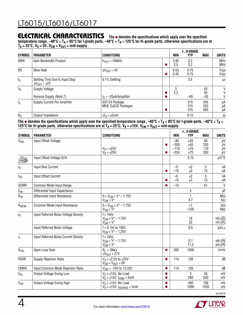
LT6015/LT6016/LT6017 1 601567ff For more information www.linear.com/LT6015 TYPICAL APPLICATION FEATURES DESCRIPTION 3.2MHz, 0.8V/µs Low Power, Over-The-Top Precision Op Amps APPLICATIONS L, LT, LTC, LTM, Linear Technology, Over-The-Top and the Linear logo are registered trademarks and ThinSOT is a trademark of Linear Technology Corporation. All other trademarks are the property of their respective owners. n Input Common Mode Range: V – to V – + 76V n Rail-to-Rail Input and Output n Low Power: 315μA/Amplifier n Operating Temperature Range: –55°C to 150°C n V OS : ±50μV (Maximum) n CMRR, PSRR: 126dB n Reverse Battery Protection to 50V n Gain Bandwidth Product: 3.2MHz n Specified on 5V and ±15V Supplies n High Voltage Gain: 1000V/mV n No Phase Reversal n No Supply Sequencing Problems n Single 5-Lead SOT-23 (ThinSOT™) Package n Dual 8-Lead MSOP n Quad 22-Lead DFN (6mm × 3mm) n High Side or Low Side Current Sensing n Battery/Power Supply Monitoring n 4mA to 20mA Transmitters n High Voltage Data Acquisition n Battery/Portable Instrumentation The LT ® 6015/LT6016/LT6017 are single/dual/quad rail-to- rail input operational amplifiers with input offset voltage trimmed to less than 50µV. These amplifiers operate on single and split supplies with a total voltage of 3V to 50V and draw only 315µA per amplifier. They are reverse battery protected, drawing very little current for reverse supplies up to 50V. The Over-The-Top ® input stage of the LT6015/LT6016/ LT6017 is designed to provide added protection in tough environments. The input common mode range extends from V – to V + and beyond: these amplifiers operate with inputs up to 76V above V – independent of V + . Internal resistors protect the inputs against transient faults up to 25V below the negative supply. The LT6015/LT6016/ LT6017 can drive loads up to 25mA and are unity-gain stable with capacitive loads as large as 200pF. Optional external compensation can be added to extend the capaci- tive drive capability beyond 200pF. The LT6015 is offered in a 5-lead SOT package. The LT6016 dual op amp is available in an 8-lead MSOP package. The LT6017 is offered in a 22-pin leadless DFN package. Precision High Voltage High Side Load Current Monitor Output Error vs Load Current – + LT6015 5V 0.1μF 200Ω 100Ω 1% 200Ω 0.1Ω 10W BSP89 1V/A 0V TO 1V OUT V BAT = 1.5V TO 76V 601567 TA01a 2k LOAD LOAD CURRENT (A) 0.01 –1.0 OUTPUT ERROR (%) 0 0.2 –0.2 –0.4 –0.6 –0.8 0.1 601567 TA01b 1 V BAT = 1.5V V BAT = 5V V BAT = 20V V BAT = 75V

Welcome message from author
This document is posted to help you gain knowledge. Please leave a comment to let me know what you think about it! Share it to your friends and learn new things together.
Transcript
LT6015/LT6016/LT6017
1601567ff
For more information www.linear.com/LT6015
Typical applicaTion
FeaTures DescripTion
3.2MHz, 0.8V/µs Low Power, Over-The-Top
Precision Op Amps
applicaTions
L, LT, LTC, LTM, Linear Technology, Over-The-Top and the Linear logo are registered trademarks and ThinSOT is a trademark of Linear Technology Corporation. All other trademarks are the property of their respective owners.
n Input Common Mode Range: V– to V– + 76Vn Rail-to-Rail Input and Outputn Low Power: 315μA/Amplifiern Operating Temperature Range: –55°C to 150°Cn VOS: ±50μV (Maximum)n CMRR, PSRR: 126dBn Reverse Battery Protection to 50Vn Gain Bandwidth Product: 3.2MHzn Specified on 5V and ±15V Suppliesn High Voltage Gain: 1000V/mVn No Phase Reversaln No Supply Sequencing Problemsn Single 5-Lead SOT-23 (ThinSOT™) Packagen Dual 8-Lead MSOPn Quad 22-Lead DFN (6mm × 3mm)
n High Side or Low Side Current Sensingn Battery/Power Supply Monitoringn 4mA to 20mA Transmittersn High Voltage Data Acquisitionn Battery/Portable Instrumentation
The LT®6015/LT6016/LT6017 are single/dual/quad rail-to-rail input operational amplifiers with input offset voltage trimmed to less than 50µV. These amplifiers operate on single and split supplies with a total voltage of 3V to 50V and draw only 315µA per amplifier. They are reverse battery protected, drawing very little current for reverse supplies up to 50V.
The Over-The-Top® input stage of the LT6015/LT6016/LT6017 is designed to provide added protection in tough environments. The input common mode range extends from V– to V+ and beyond: these amplifiers operate with inputs up to 76V above V– independent of V+. Internal resistors protect the inputs against transient faults up to 25V below the negative supply. The LT6015/LT6016/LT6017 can drive loads up to 25mA and are unity-gain stable with capacitive loads as large as 200pF. Optional external compensation can be added to extend the capaci-tive drive capability beyond 200pF.
The LT6015 is offered in a 5-lead SOT package. The LT6016 dual op amp is available in an 8-lead MSOP package. The LT6017 is offered in a 22-pin leadless DFN package.
Precision High Voltage High Side Load Current Monitor Output Error vs Load Current
–
+LT6015
5V0.1µF
200Ω100Ω1%
200Ω0.1Ω10W BSP89
1V/A0V TO 1V OUT
VBAT = 1.5V TO 76V
601567 TA01a
2kLOAD
LOAD CURRENT (A)0.01
–1.0
OUTP
UT E
RROR
(%)
0
0.2
–0.2
–0.4
–0.6
–0.8
0.1
601567 TA01b
1
VBAT = 1.5VVBAT = 5VVBAT = 20VVBAT = 75V
LT6015/LT6016/LT6017
2601567ff
For more information www.linear.com/LT6015
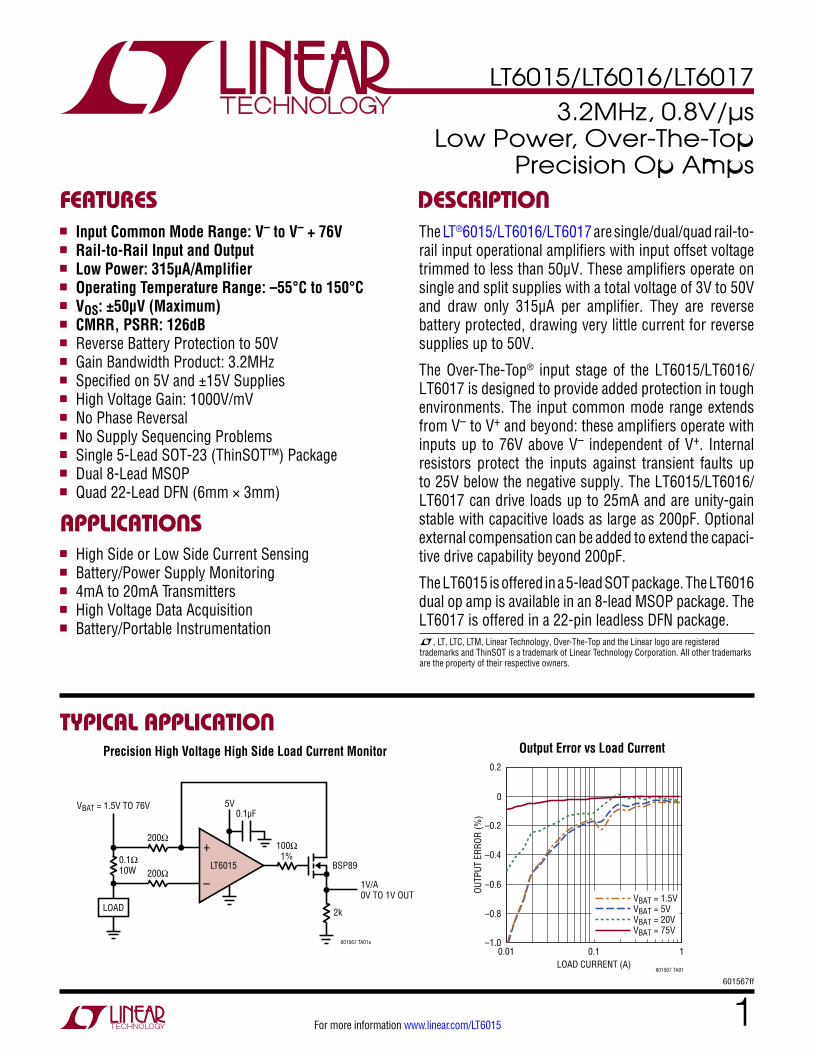
pin conFiguraTion
absoluTe MaxiMuM raTings (Note 1)
22
21
20
19
18
17
16
15
14
13
12
1
2
3
4
5
6
7
8
9
10
11
OUTD
–IND
+IND
N/C
V–
N/C
V–
N/C
+INC
–INC
OUTC
OUTA
–INA
+INA
N/C
V+
N/C
V+
N/C
+INB
–INB
OUTB
TOP VIEW
23
DJC PACKAGE22-LEAD (6mm × 3mm) PLASTIC DFN
B C
A D
TJMAX = 150°C, JA = 31.8°C/W, JC = 4.3°C/W
CONNECT UNDERSIDE METAL TO V–
1234
OUTA–INA+INA
V–
8765
V+
OUTB–INB+INB
TOP VIEW
MS8 PACKAGE8-LEAD PLASTIC MSOP
BA
TJMAX = 150°C, JA = 273°C/W, JC = 45°C/W
OUT 1
V– 2
TOP VIEW
S5 PACKAGE5-LEAD PLASTIC TSOT-23
+IN 3
5 V+
4 –IN
TJMAX = 150°C, JA = 250°C/W
orDer inForMaTion
LEAD FREE FINISH TAPE AND REEL PART MARKING* PACKAGE DESCRIPTION TEMPERATURE RANGE
LT6016IMS8#PBF LT6016IMS8#TRPBF LTGFK 8-Lead Plastic MSOP –40°C to 85°C
LT6016HMS8#PBF LT6016HMS8#TRPBF LTGFK 8-Lead Plastic MSOP –40°C to 125°C
LT6016MPMS8#PBF LT6016MPMS8#TRPBF LTGFK 8-Lead Plastic MSOP –55°C to 150°C
LT6017IDJC#PBF LT6017IDJC#TRPBF 6017 22-Lead Plastic DFN –40°C to 85°C
LT6017HDJC#PBF LT6017HDJC#TRPBF 6017 22-Lead Plastic DFN –40°C to 125°C
LT6017MPDJC#PBF LT6017MPDJC#TRPBF 6017 22-Lead Plastic DFN –55°C to 150°C
Consult LTC Marketing for parts specified with wider operating temperature ranges. *The temperature grade is identified by a label on the shipping container.For more information on lead free part marking, go to: http://www.linear.com/leadfree/ For more information on tape and reel specifications, go to: http://www.linear.com/tapeandreel/
Supply Voltage (V+ to V–) ................................60V, –50VInput Differential Voltage ........................................±80VInput Voltage (Note 2) .....................................80V, –25VInput Current (Note 2) .......................................... ±10mAOutput Short-Circuit Duration(Note 3) ......................................................... Continuous
Temperature Range (Notes 4, 5) LT6015I/LT6016I/LT6017I ....................–40°C to 85°C LT6015H/LT6016H/LT6017H .............. –40°C to 125°C LT6015MP/LT6016MP/LT6017MP
(TJUNCTION) ........................................ –55°C to 150°CStorage Temperature Range .................. –65°C to 150°CMaximum Junction Temperature .......................... 150°CLead Temperature (Soldering, 10sec).................... 300°C
Lead Free FinishTAPE AND REEL (MINI) TAPE AND REEL PART MARKING* PACKAGE DESCRIPTION TEMPERATURE RANGE
LT6015IS5#TRMPBF LT6015IS5#TRPBF LTGJD 5-Lead Plastic TSOT-23 –40°C to 85°C
LT6015HS5#TRMPBF LT6015HS5#TRPBF LTGJD 5-Lead Plastic TSOT-23 –40°C to 125°C
LT6015MPS5#TRMPBF LT6015MPS5#TRPBF LTGJD 5-Lead Plastic TSOT-23 –55°C to 150°CTRM = 500 pieces. Consult LTC Marketing for information on lead based finish parts.
LT6015/LT6016/LT6017
3601567ff
For more information www.linear.com/LT6015
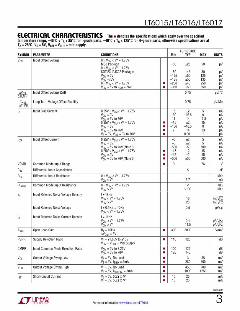
The l denotes the specifications which apply over the specified temperature range, –40°C < TA < 85°C for I-grade parts, –40°C < TA < 125°C for H–grade parts, otherwise specifications are at TA = 25°C, VS = 5V, VCM = VOUT = mid-supply.
elecTrical characTerisTics
SYMBOL PARAMETER CONDITIONS MINI-, H-GRADE
TYP MAX UNITSVOS Input Offset Voltage 0 < VCM < V+ – 1.75V
MS8 Package 0 < VCM < V+ – 1.75V SOT-23, DJC22 Packages VCM = 5V VCM =76V 0 < VCM < V+ – 1.75V VCM = 5V to VCM = 76V
l
l
–50
–80
–125 –135 –250 –350
±25
±45 ±50 ±50 ±45 ±50
50
80 125 135 250 350
µV
µV µV µV µV µV
∆VOS ∆TEMP
Input Offset Voltage Drift 0.75 µV/°C
∆VOS ∆TIME
Long Term Voltage Offset Stability 0.75 µV/Mo
IB Input Bias Current 0.25V < VCM < V+ – 1.75V VCM = 0V VCM = 5V to 76V 0.25V < VCM < V+ – 1.75V VCM = 0V VCM = 5V to 76V VS = 0V, VCM = 0V to 76V
l
l
l
l
–5 –60 11
–15 –150
7
±2 –16.5
14 ±2
–16.5 14
0.001
5 0
17.5 15 0
23 1
nA nA µA nA nA µA µA
IOS Input Offset Current 0.25V < VCM < V+ – 1.75V VCM = 0V VCM = 5V to 76V (Note 6) 0.25V < VCM < V+ – 1.75V VCM = 0V VCM = 5V to 76V (Note 6)
l
l
l
–5 –5
–500 –15 –15
–500
±2 ±2
±50 ±2 ±2
±50
5 5
500 15 15
500
nA nA nA nA nA nA
VCMR Common Mode Input Range l 0 76 V
CIN Differential Input Capacitance 5 pF
RIN Differential Input Resistance 0 < VCM < V+ – 1.75V VCM > V+
1 3.7
MΩ kΩ
RINCM Common Mode Input Resistance 0 < VCM < V+ – 1.75V VCM > V+
>1 >100
GΩ MΩ
en Input Referred Noise Voltage Density f = 1kHz VCM < V+ – 1.75V VCM > V+
18 25
nV/√Hz nV/√Hz
Input Referred Noise Voltage f = 0.1Hz to 10Hz VCM < V+ – 1.75V
0.5 µVP-P
in Input Referred Noise Current Density f = 1kHz VCM < V+ – 1.75V VCM > V+
0.1
11.5
pA/√Hz pA/√Hz
AVOL Open Loop Gain RL = 10kΩ ∆VOUT = 3V
l 300 3000 V/mV
PSRR Supply Rejection Ratio VS = ±1.65V to ±15V VCM = VOUT = Mid-Supply
l 110 126 dB
CMRR Input Common Mode Rejection Ratio VCM = 0V to 3.25V VCM = 5V to 76V
l
l
100 126
126 140
dB dB
VOL Output Voltage Swing Low VS = 5V, No Load VS = 5V, ISINK = 5mA
l
l
3 280
55 500
mV mV
VOH Output Voltage Swing High VS = 5V, No Load VS = 5V, ISOURCE = 5mA
l
l
450 1000
700 1250
mV mV
ISC Short-Circuit Current VS = 5V, 50Ω to V+ VS = 5V, 50Ω to V–
l
l
10 10
25 25
mA mA
LT6015/LT6016/LT6017
4601567ff
For more information www.linear.com/LT6015
elecTrical characTerisTics The l denotes the specifications which apply over the specified temperature range, –40°C < TA < 85°C for I-grade parts, –40°C < TA < 125°C for H–grade parts, otherwise specifications are at TA = 25°C, VS = 5V, VCM = VOUT = mid-supply.
SYMBOL PARAMETER CONDITIONS MINI-, H-GRADE
TYP MAX UNITSVOSI Input Offset Voltage
VS = ±25V VS = ±25V
l
l
–80 –250 –110 –250
±55 ±55 ±75 ±75
80 250 110 250
µV µV µV µV
∆VOSI ∆TEMP
Input Offset Voltage Drift 0.75 µV/°C
IB Input Bias Current
l
–5 –15
±2 ±2
5 15
nA nA
IOS Input Offset Current
l
–5 –15
±2 ±2
5 15
nA nA
VCMR Common Mode Input Range l –15 61 VCIN Differential Input Capacitance 5 pFRIN Differential Input Resistance 0 < VCM < V+ – 1.75V
VCM > V+1
3.7MΩ kΩ
RINCM Common Mode Input Resistance 0 < VCM < V+ – 1.75V VCM > V+
>1 >100
GΩ MΩ
en Input Referred Noise Voltage Density f = 1kHz VCM < V+ – 1.75V VCM > V+
18 25
nV/√Hz nV/√Hz
Input Referred Noise Voltage f = 0.1Hz to 10Hz VCM < V+ – 1.25V
0.5 µVP-P
in Input Referred Noise Current Density f = 1kHz VCM < V+ – 1.75V VCM > V+
0.1
11.5
pA/√Hz pA/√Hz
AVOL Open Loop Gain RL = 10kΩ ∆VOUT = 27V
l 200 1000 V/mV
PSRR Supply Rejection Ratio
VS = ±2.5V to ±25V VCM = VOUT = 0V
l 114 126 dB
CMRR Input Common Mode Rejection Ratio VCM = –15V to 13.25V l 110 126 dBVOL Output Voltage Swing Low VS = ±15V, No Load
VS = ±15V, ISINK = 5mAl
l
3 280
55 500
mV mV
VOH Output Voltage Swing High VS = ±15V, No Load VS = ±15V, ISOURCE = 5mA
l
l
450 1000
700 1250
mV mV
The l denotes the specifications which apply over the specified temperature range, –40°C < TA < 85°C for I-grade parts, –40°C < TA < 125°C for H–grade parts, otherwise specifications are at TA = 25°C, VS = ±15V, VCM = VOUT = mid-supply.
SYMBOL PARAMETER CONDITIONS MINI-, H-GRADE
TYP MAX UNITSGBW Gain Bandwidth Product fTEST = 100kHz
l
2.85 2.5
3.2 3.2
MHz MHz
SR Slew Rate ∆VOUT = 3V
l
0.55 0.45
0.75 0.75
V/µs V/µs
tS Settling Time Due to Input Step ∆VOUT = ±2V
0.1% Settling 3.5 µs
VS Supply Voltage Reverse Supply (Note 7)
IS < –25µA/Amplifier
l
l
3 3.3
–65
50 50
–50
V V V
IS Supply Current Per Amplifier SOT-23 Package MS8, DJC22 Packages
l
315 315 315
345 335 500
µA µA µA
RO Output Impedance ∆IO = ±5mA 0.15 Ω
LT6015/LT6016/LT6017
5601567ff
For more information www.linear.com/LT6015
elecTrical characTerisTics The l denotes the specifications which apply over the specified temperature range, –40°C < TA < 85°C for I-grade parts, –40°C < TA < 125°C for H–grade parts, otherwise specifications are at TA = 25°C, VS = ±15V, VCM = VOUT = mid-supply.
SYMBOL PARAMETER CONDITIONS
MINMP-GRADE
TYP
MAX UNITSVOS Input Offset Voltage 0 < VCM < V+ – 1.75V
MS8 Package 0 < VCM < V+ – 1.75V DJC22 Package VCM = 5V VCM = 76V 0 < VCM < V+ –1.75V VCM = 5V to VCM = 76V
l
l
–50
–80
–125 –135 –500 –600
±25
±45 ±50 ±50 ±45 ±50
50
80 125 135 500 600
µV µV
µV µV µV µV µV
∆VOS ∆TEMP
Input Offset Voltage Drift 0.75 µV/°C
∆VOS ∆TIME
Long Term Voltage Offset Stability 0.75 µV/Mo
IB Input Bias Current 0.25V < VCM < V+ – 1.75V VCM = 0V VCM = 5V to 76V 0.25V < VCM < V+ – 1.75V VCM = 0V VCM = 5V to 76V VS = 0V, VCM = 0V to 76V
l
l
l
l
–5 –60 11
–100 –500 6.5
±2 –16.5
14 ±2
–16.5 14
0.001
5 0
17.5 100
0 24 4
nA nA µA nA nA µA µA
IOS Input Offset Current 0.25V < VCM < V+ – 1.75V VCM = 0V VCM = 5V to 76V (Note 6) 0.25V < VCM < V+ – 1.75V VCM = 0V VCM = 5V to 76V (Note 6)
l
l
l
–5 –5
–500 –50
–200 –500
±2 ±2
±50 ±2 ±2
±150
5 5
500 50
200 500
nA nA nA nA nA nA
VCMR Common Mode Input Range l 0 76 VCIN Differential Input Capacitance 5 pFRIN Differential Input Resistance 0 < VCM < V+ – 1.75V
VCM > V+1
3.7MΩ kΩ
RINCM Common Mode Input Resistance 0 < VCM < V+ – 1.75V VCM > V+
>1 >100
GΩ MΩ
The l denotes the specifications which apply over the specified temperature range, –55°C < TJUNCTION < 150°C for MP-grade parts, otherwise specifications are at TA = 25°C, VS = 5V, VCM = VOUT = mid-supply.
SYMBOL PARAMETER CONDITIONS MINI-, H-GRADE
TYP MAX UNITSISC Short-Circuit Current VS = ±15V, 50Ω to GND
VS = ±15V, 50Ω to GNDl
l
10 10
30 32
mA mA
GBW Gain Bandwidth Product fTEST = 100kHz
l
2.9 2.55
3.3 3.3
MHz MHz
SR Slew Rate ∆VOUT = 3V
l
0.6 0.5
0.8 0.8
V/µs V/µs
tS Settling Time Due to Input Step 0.1% Settling ∆VOUT = ±2V
3.5 µs
VS Supply Voltage Reverse Supply
IS = –25µA/Amplifier
l
l
3 3.3
–65
50 50
–30
V V V
IS Supply Current Per Amplifier SOT-23 Package MS8, DJC22 Packages VS = ±25V, SOT-23 Package VS = ±25V, MS8, DJC22 Package VS = ±25V
l
l
325 325 325 340 340 340
360 350 525 370 360 550
µA µA µA µA µA µA
RO Output Impedance ∆IO = ±5mA 0.15 Ω
LT6015/LT6016/LT6017
6601567ff
For more information www.linear.com/LT6015
elecTrical characTerisTics The l denotes the specifications which apply over the specified temperature range, –55°C < TJUNCTION < 150°C for MP-grade parts, otherwise specifications are at TA = 25°C, VS = 5V, VCM = VOUT = mid-supply.
SYMBOL PARAMETER CONDITIONS MINMP-GRADE
TYP MAX UNITS
VOSI Input Offset Voltage VS = ±25V VS = ±25V
l
l
–80 –500 –110 –500
±55 ±55 ±75 ±75
80 500 110 500
µV µV µV µV
∆VOSI ∆TEMP
Input Offset Voltage Drift 0.75 µV/°C
IB Input Bias Current
l
–5 –300
±2 ±2
5 300
nA nA
IOS Input Offset Current
l
–5 –50
±2 ±2
5 50
nA nA
VCMR Common Mode Input Range l –15 61 V
CIN Differential Input Capacitance 5 pF
RIN Differential Input Resistance 0 < VCM < V+ – 1.75V VCM > V+
1 3.7
MΩ kΩ
The l denotes the specifications which apply over the specified temperature range, –55°C < TJUNCTION < 150°C for MP-grade parts, otherwise specifications are at TA = 25°C, VS = ±15V, VCM = VOUT = mid-supply.
SYMBOL PARAMETER CONDITIONS
MINMP-GRADE
TYP
MAX UNITSen Input Referred Noise Voltage Density f = 1kHz
VCM < V+ – 1.75V VCM > V+
18 25
nV/√Hz nV/√Hz
Input Referred Noise Voltage f = 0.1Hz to 10Hz VCM < V+ – 1.75V
0.5 µVP-P
in Input Referred Noise Current Density f = 1kHz VCM < V+ – 1.75V VCM > V+
0.1
11.5
pA/√Hz pA/√Hz
AVOL Open Loop Gain RL = 10kΩ ∆VOUT = 3V
l 200 3000 V/mV
PSRR Supply Rejection Ratio VS = ±1.65V to ±15V VCM = VOUT = Mid-Supply
l 106 126 dB
CMRR Input Common Mode Rejection Ratio VCM = 0V to 3.25V VCM = 5V to 76V
l
l
90 120
126 140
dB dB
VOL Output Voltage Swing Low VS = 5V, No Load VS = 5V, ISINK = 5mA
l
l
3 280
75 550
mV mV
VOH Output Voltage Swing High VS = 5V, No Load VS = 5V, ISOURCE = 5mA
l
l
450 1000
750 1300
mV mV
ISC Short-Circuit Current VS = 5V, 50Ω to V+ VS = 5V, 50Ω to V–
l
l
8 8
25 25
mA mA
GBW Gain Bandwidth Product fTEST = 100kHz
l
2.85 2.4
3.2 3.2
MHz MHz
SR Slew Rate ∆VOUT = 3V
l
0.55 0.4
0.75 0.75
V/µs V/µs
tS Settling Time Due to Input Step 0.1% Settling ∆VOUT = ±2V
3.5 µs
VS Supply Voltage Reverse Supply (Note 7)
IS < –25VµA/Amplifier
l
l
3 3.3
–63
50 50
–50
V V V
IS Supply Current Per Amplifier SOT-23 Package MS8, DJC22 Packages
l
315 315 315
345 335 540
µA µA µA
RO Output Impedance ∆IO = ±5mA 0.15 Ω
LT6015/LT6016/LT6017
7601567ff
For more information www.linear.com/LT6015
The l denotes the specifications which apply over the specified temperature range, –55°C < TJUNCTION < 150°C for MP-grade parts, otherwise specifications are at TA = 25°C, VS = ±15V, VCM = VOUT = Mid-Supply.elecTrical characTerisTics
SYMBOL PARAMETER CONDITIONS MINMP-GRADE
TYP MAX UNITSRINCM Common Mode Input Resistance 0 < VCM < V+ – 1.75V
VCM > V+>1
>100GΩ MΩ
en Input Referred Noise Voltage Density f = 1kHz VCM < V+ – 1.75V VCM > V+
18 25
nV/√Hz nV/√Hz
Input Referred Noise Voltage f = 0.1Hz to 10Hz VCM < V+ – 1.75V
0.5 µVP-P
in Input Referred Noise Current Density f = 1kHz VCM < V+ – 1.75V VCM > V+
0.1
11.5
pA/√Hz pA/√Hz
AVOL Open Loop Gain RL = 10kΩ ∆VOUT = 27V
l 100 1000 V/mV
PSRR Supply Rejection Ratio VS = ±2.5V to ±25V VCM = VOUT = 0V
l 106 126 dB
CMRR Input Common Mode Rejection Ratio VCM = –15V to 13.25V l 100 126 dBVOL Output Voltage Swing Low VS = ±15V, No Load
VS = ±15V, ISINK = 5mAl
l
3 280
75 550
mV mV
VOH Output Voltage Swing High VS = ±15V, No Load VS = ±15V, ISOURCE = 5mA
l
l
450 1000
750 1300
mV mV
ISC Short-Circuit Current VS = ±15V, 50Ω to GND VS = ±15V, 50Ω to GND
l
l
8 8
30 32
mA mA
GBW Gain Bandwidth Product fTEST = 100kHz
l
2.9 2.45
3.3 3.3
MHz MHz
SR Slew Rate ∆VOUT = 3V
l
0.6 0.45
0.8 0.8
V/µs V/µs
tS Settling Time Due to Input Step 0.1% Settling ∆VOUT = ±2V
3.5 µs
VS Supply Voltage Reverse Supply
IS = –25µA/Amplifier
l
l
3 3.3
–65
50 50
–30
V V V
IS Supply Current Per Amplifier SOT-23 Package MS8, DJC22 Packages VS = ±25V, SOT-23 Package VS = ±25V, MS8, DJC22 Package VS = ±25V
l
l
325 325 325 340 340 340
360 350 575 370 360 600
µA µA µA µA µA µA
RO Output Impedance ∆IO = ±5mA 0.15 Ω
Note 1: Stresses beyond those listed under Absolute Maximum Ratings may cause permanent damage to the device. Exposure to any Absolute Maximum Rating condition for extended periods may affect device reliability and lifetime.Note 2: Voltages applied are with respect to V–. The inputs are tested to the Absolute Maximum Rating by applying –25V (relative to V–) to each input for 10ms. In general, faults capable of sinking current from either input should be current limited to under 10mA. See the Applications Information section for more details.Note 3: A heat sink may be required to keep the junction temperature below absolute maximum. This depends on the power supply voltage and how many amplifiers are shorted.Note 4: The LT6015I/LT6016I/LT6017I are guaranteed functional over the oper-ating temperature range of –40°C to 85°C. The LT6015H/LT6016H/LT6017H are guaranteed functional over the operating temperature range of –40°C to 125°C.
The LT6015MP/LT6016MP/LT6017MP are guaranteed functional over the junction temperature range of –55°C to 150°C. Junction temperatures greater than 125°C will promote accelerated aging. The LT6015/LT6016/LT6017 has a demonstrated typical performance beyond 1000 hours at TJ = 150°C.Note 5: The LT6015I/LT6016I/LT6017I are guaranteed to meet specified performance from –40°C to 85°C. The LT6015H/LT6016H/LT6017H are guaranteed to meet specified performance from –40°C to 125°C. The LT6015MP/LT6016MP/LT6017MP are guaranteed to meet specified performance with junction temperature ranging from –55°C to 150°C.Note 6: Test accuracy is limited by high speed test equipment repeatability. Bench measurements indicate the input offset current in the Over-The-Top configuration is typically controlled to under ±50nA at 25°C and ±150nA over temperature.Note 7: The Reverse Supply voltage is tested by pulling 25μA/Amplifier out of the V+ pin while measuring the V+ pin’s voltage with both inputs and V– grounded, verifying V+ < –50V.
LT6015/LT6016/LT6017
8601567ff
For more information www.linear.com/LT6015
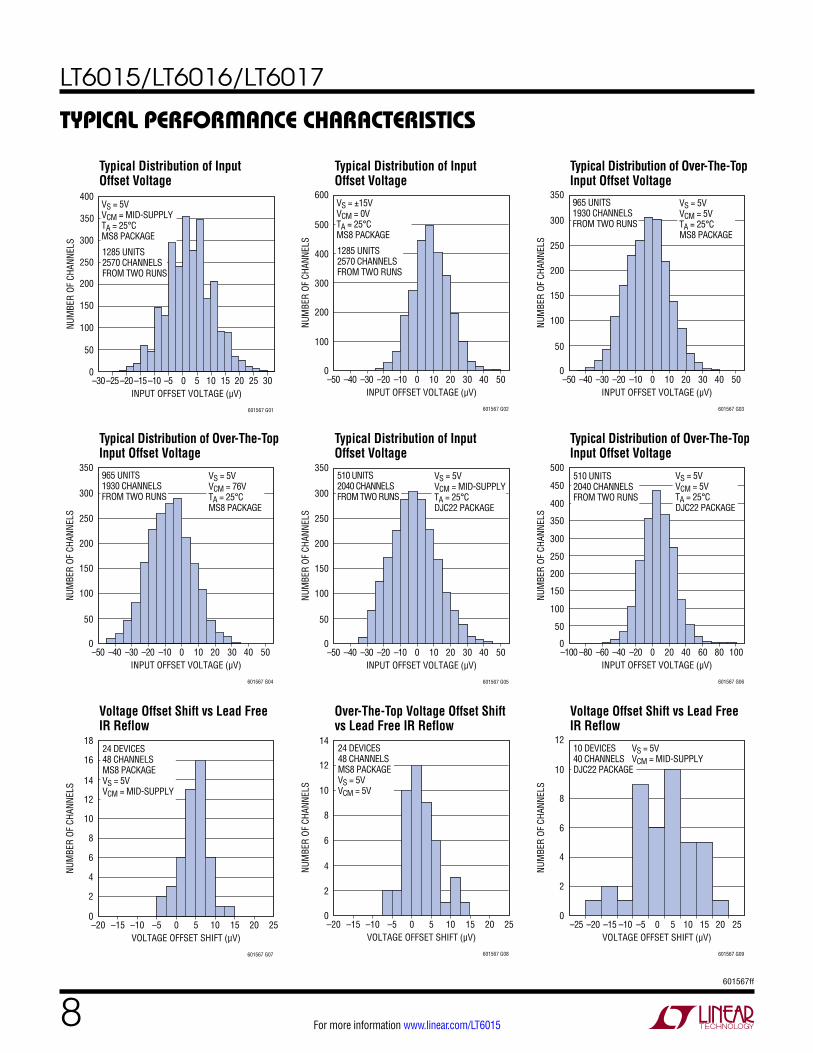
Typical perForMance characTerisTics
Typical Distribution of Over-The-Top Input Offset Voltage
Typical Distribution of Input Offset Voltage
Typical Distribution of Over-The-Top Input Offset Voltage
Voltage Offset Shift vs Lead Free IR Reflow
Over-The-Top Voltage Offset Shift vs Lead Free IR Reflow
Voltage Offset Shift vs Lead Free IR Reflow
Typical Distribution of Input Offset Voltage
Typical Distribution of Input Offset Voltage
Typical Distribution of Over-The-Top Input Offset Voltage
INPUT OFFSET VOLTAGE (µV)–50 –40 –30 –20 –10
0
NUM
BER
OF C
HANN
ELS
600
500
400
300
200
100
0 10 20 30 40 50
601567 G02
VS = ±15VVCM = 0VTA = 25°CMS8 PACKAGE
1285 UNITS2570 CHANNELSFROM TWO RUNS
INPUT OFFSET VOLTAGE (µV)–50 –40 –30 –20 –10
0
NUM
BER
OF C
HANN
ELS
350
300
250
200
150
100
50
0 10 20 30 40 50
601567 G03
VS = 5VVCM = 5VTA = 25°CMS8 PACKAGE
965 UNITS1930 CHANNELSFROM TWO RUNS
INPUT OFFSET VOLTAGE (µV)–50 –40 –30 –20 –10
0
NUM
BER
OF C
HANN
ELS
350
300
250
200
150
100
50
0 10 20 30 40 50
601567 G05
VS = 5VVCM = MID-SUPPLYTA = 25°CDJC22 PACKAGE
510 UNITS2040 CHANNELSFROM TWO RUNS
INPUT OFFSET VOLTAGE (µV)–100 –80 –60 –40 –200
NUM
BER
OF C
HANN
ELS
500
450
400
350
300
250
200
150
100
50
0 20 40 60 80 100
601567 G06
VS = 5VVCM = 5VTA = 25°CDJC22 PACKAGE
510 UNITS2040 CHANNELSFROM TWO RUNS
VOLTAGE OFFSET SHIFT (µV)–20 –15 –10 –5
0
NUM
BER
OF C
HANN
ELS
18
16
14
12
10
8
6
4
2
0 5 10 15 20 25
601567 G07
24 DEVICES48 CHANNELSMS8 PACKAGEVS = 5VVCM = MID-SUPPLY
VOLTAGE OFFSET SHIFT (µV)–20 –15 –10 –5
0
NUM
BER
OF C
HANN
ELS
14
12
10
8
6
4
2
0 5 10 15 20 25
601567 G08
24 DEVICES48 CHANNELSMS8 PACKAGEVS = 5VVCM = 5V
INPUT OFFSET VOLTAGE (µV)–30–25–20–15–10 –5
0
NUM
BER
OF C
HANN
ELS
350
400
300
250
200
150
100
50
0 5 10 15 20 25 30
601567 G01
VS = 5VVCM = MID-SUPPLYTA = 25°CMS8 PACKAGE
1285 UNITS2570 CHANNELSFROM TWO RUNS
INPUT OFFSET VOLTAGE (µV)–50 –40 –30 –20 –10
0
NUM
BER
OF C
HANN
ELS
350
300
250
200
150
100
50
0 10 20 30 40 50
601567 G04
VS = 5VVCM = 76VTA = 25°CMS8 PACKAGE
965 UNITS1930 CHANNELSFROM TWO RUNS
VOLTAGE OFFSET SHIFT (µV)–25 –20 –5 0
0
NUM
BER
OF C
HANN
ELS
12
10
8
6
4
2
–15 –10 5 10 15 20 25
601567 G09
10 DEVICES40 CHANNELSDJC22 PACKAGE
VS = 5VVCM = MID-SUPPLY
LT6015/LT6016/LT6017
9601567ff
For more information www.linear.com/LT6015
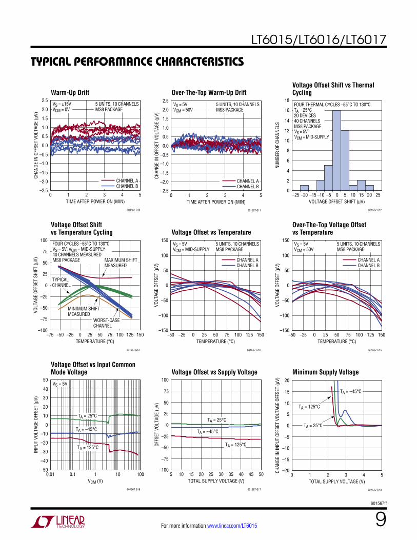
Typical perForMance characTerisTics
Voltage Offset Shift vs Temperature Cycling Voltage Offset vs Temperature
Over-The-Top Voltage Offset vs Temperature
Voltage Offset vs Input Common Mode Voltage Voltage Offset vs Supply Voltage Minimum Supply Voltage
Warm-Up Drift Over-The-Top Warm-Up DriftVoltage Offset Shift vs Thermal Cycling
TIME AFTER POWER ON (MIN)10 2
–2.5
CHAN
GE IN
OFF
SET
VOLT
AGE
(µV)
2.5
2.0
1.5
1.0
0.5
0.0
–0.5
–1.0
–1.5
–2.0
3 54
601567 G10
VS = ±15VVCM = 0V
5 UNITS, 10 CHANNELSMS8 PACKAGE
CHANNEL ACHANNEL B
TIME AFTER POWER ON (MIN)10 2
–2.5
CHAN
GE IN
OFF
SET
VOLT
AGE
(µV)
2.5
2.0
1.5
1.0
0.5
0.0
–0.5
–1.0
–1.5
–2.0
3 54
601567 G11
VS = 5VVCM = 50V
5 UNITS, 10 CHANNELSMS8 PACKAGE
CHANNEL ACHANNEL B
VCM (V)0.01
–50
INPU
T VO
LTAG
E OF
FSET
(µV)
40
50
30
20
10
0
–10
–20
–30
–40
0.1 1 10
601567 G16
100
TA = 25°C
TA = –45°C
TA = 125°C
VS = 5V
TOTAL SUPPLY VOLTAGE (V)5 10 15 20 30 35
–100
OFFS
ET V
OLTA
GE (µ
V)
75
100
50
25
0
–25
–50
–75
25 4540
601567 G17
50
TA = 25°C
TA = –45°C
TA = 125°C
TOTAL SUPPLY VOLTAGE (V)0 1 3
–20CHAN
GE IN
INPU
T OF
FSET
VOL
TAGE
OFF
SET
(µV)
15
20
10
5
0
–5
–10
–15
2 4
601567 G18
5
TA = 25°C
TA = –45°C
TA = 125°C
VOLTAGE OFFSET SHIFT (µV)–25 –20 –5 0
0
NUM
BER
OF C
HANN
ELS
18
16
14
12
10
8
6
4
2
–15 –10 5 10 15 20 25
601567 G12
FOUR THERMAL CYCLES –55°C TO 130°CTA = 25°C20 DEVICES40 CHANNELSMS8 PACKAGEVS = 5VVCM = MID-SUPPLY
TEMPERATURE (°C)–25 0
–100
VOLT
AGE
OFFS
ET S
HIFT
(µV)
100
75
50
25
0
–25
–50
–75
–50–75 25 50 75 100 125 150
601567 G13
FOUR CYCLES –55°C TO 130°CVS = 5V, VCM = MID-SUPPLY40 CHANNELS MEASUREDMS8 PACKAGE
TYPICALCHANNEL
MINIMUM SHIFTMEASURED
WORST-CASECHANNEL
MAXIMUM SHIFTMEASURED
TEMPERATURE (°C)–25–50 0 25
–150
VOLT
AGE
OFFS
ET (µ
V)
150
100
50
0
–50
–100
50 150100 12575
601567 G14
VS = 5VVCM = MID-SUPPLY
5 UNITS, 10 CHANNELSMS8 PACKAGE
CHANNEL ACHANNEL B
TEMPERATURE (°C)–25–50 0 25
–150
VOLT
AGE
OFFS
ET (µ
V)
150
100
50
0
–50
–100
50 150100 12575
601567 G15
VS = 5VVCM = 50V
5 UNITS, 10 CHANNELSMS8 PACKAGE
CHANNEL ACHANNEL B
LT6015/LT6016/LT6017
10601567ff
For more information www.linear.com/LT6015
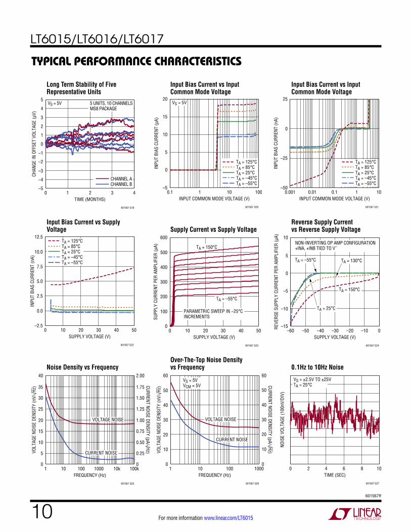
Typical perForMance characTerisTics
Input Bias Current vs Supply Voltage Supply Current vs Supply Voltage
Reverse Supply Current vs Reverse Supply Voltage
Noise Density vs FrequencyOver-The-Top Noise Density vs Frequency 0.1Hz to 10Hz Noise
Long Term Stability of Five Representative Units
Input Bias Current vs Input Common Mode Voltage
Input Bias Current vs Input Common Mode Voltage
SUPPLY VOLTAGE (V)–60
–15REVE
RSE
SUPP
LY C
URRE
NT P
ER A
MPL
IFIE
R (µ
A) 10
0
5
–5
–10
–50 –40 –30 –20
601567 G24
0–10
TA = 130°C
NON-INVERTING OP AMP CONFIGURATION +INA, +INB TIED TO V–
TA = –55°C
TA = 25°C
TA = 150°C
TIME (MONTHS)10 2
–5
CHAN
GE IN
OFF
SET
VOLT
AGE
(µV)
5
4
3
2
1
0
–1
–2
–3
–4
3 4
601567 G19
VS = 5V 5 UNITS, 10 CHANNELSMS8 PACKAGE
CHANNEL ACHANNEL B
FREQUENCY (Hz)1
0
VOLT
AGE
NOIS
E DE
NSIT
Y (n
V/√H
z)
CURRENT NOISE DENSITY (pA/√Hz)
60
50
40
30
20
10
0
60
50
40
30
20
10
10 100 1000
601567 G26
VS = 5VVCM = 5V
CURRENT NOISE
VOLTAGE NOISE
TIME (SEC)0
NOIS
E VO
LTAG
E (1
00nV
/DIV
)
2 64 8 10
601567 G27
VS = ±2.5V TO ±25VTA = 25°C
SUPPLY VOLTAGE (V)0
0
SUPP
LY C
URRE
NT P
ER A
MPL
IFIE
R (µ
A)
600
400
300
500
200
100
10 20 30 40
601567 G23
50
TA = –55°C
TA = 150°C
PARAMETRIC SWEEP IN ~25°C INCREMENTS
FREQUENCY (Hz)1
0
VOLT
AGE
NOIS
E DE
NSIT
Y (n
V/√H
z)
CURRENT NOISE DENSITY (pA/√Hz)
40
35
30
25
20
15
10
5
0
2.00
1.75
1.50
1.25
1.00
0.75
0.50
0.25
10 100 1000 10k
601567 G25
100k
CURRENT NOISE
VOLTAGE NOISE
INPUT COMMON MODE VOLTAGE (V)0.1
–5
INPU
T BI
AS C
URRE
NT (µ
A)
20
15
10
5
0
1 10
601567 G20
100
TA = 125°CTA = 85°CTA = 25°CTA = –45°CTA = –55°C
VS = 5V
INPUT COMMON MODE VOLTAGE (V)0.001
–50
INPU
T BI
AS C
URRE
NT (n
A)
25
0
–25
0.01 0.1 1
601567 G21
10
TA = 125°CTA = 85°CTA = 25°CTA = –45°CTA = –55°C
SUPPLY VOLTAGE (V)0
–2.5
INPU
T BI
AS C
URRE
NT (n
A)
12.5
7.5
5.0
10.0
2.5
0.0
10 20 30 40
601567 G22
50
TA = 125°CTA = 85°CTA = 25°CTA = –45°CTA = –55°C
LT6015/LT6016/LT6017
11601567ff
For more information www.linear.com/LT6015
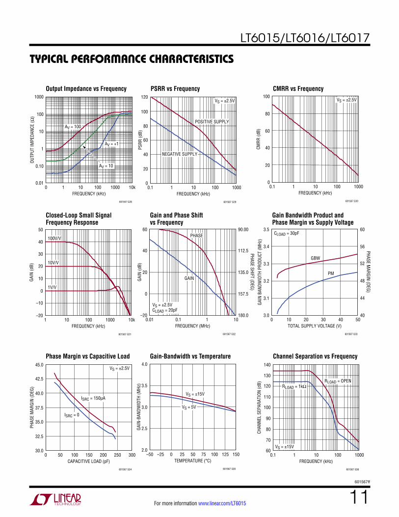
Typical perForMance characTerisTics
Closed-Loop Small Signal Frequency Response
Gain and Phase Shift vs Frequency
Gain Bandwidth Product and Phase Margin vs Supply Voltage
Phase Margin vs Capacitive Load Gain-Bandwidth vs Temperature Channel Separation vs Frequency
Output Impedance vs Frequency PSRR vs Frequency CMRR vs Frequency
FREQUENCY (kHz)0.1
0
CMRR
(dB)
100
80
60
40
20
1 10 100 1000
601567 G30
VS = ±2.5V
FREQUENCY (kHz)1
–20
GAIN
(dB)
50
40
30
20
10
0
–10
10 100 1000 10k
601567 G31
100V/V
10V/V
1V/V
CAPACITIVE LOAD (pF)0
30.0
PHAS
E M
ARGI
N (D
EG)
45.0
42.5
40.0
37.5
35.0
32.5
50 100 150 200 250 300
601567 G34
VS = ±2.5V
ISRC = 150µA
ISRC = 0
FREQUENCY (kHz)0.1
60
CHAN
NEL
SEPA
RATI
ON (d
B)
140
130
120
110
100
90
80
70
1 10 100 1000
601567 G36
RLOAD = OPEN
VS = ±15V
RLOAD = 1kΩ
FREQUENCY (kHz)0
0.01
OUTP
UT IM
PEDA
NCE
(Ω)
1000
100
10
1
0.10
1 10 100 1000
601567 G28
10k
AV = 100
AV = 10
AV = +1
FREQUENCY (kHz)0.1
0
PSRR
(dB)
120
100
80
60
40
20
1 10 100 1000
601567 G29
POSITIVE SUPPLY
NEGATIVE SUPPLY
VS = ±2.5V
FREQUENCY (MHz)0.01
–20
GAIN
(dB)
PHASE SHIFT (DEG)
60
40
20
0
180.0
90.00
112.5
135.0
157.5
0.1 1 10
601567 G32
GAIN
PHASE
VS = ±2.5VCLOAD = 20pF
TEMPERATURE (°C)–50
2.0
GAIN
-BAN
DWID
TH (M
Hz)
4.0
3.5
3.0
2.5
–25 0 25 50 75 100 125 150
601567 G35
VS = ±15V
VS = 5V
TOTAL SUPPLY VOLTAGE (V)0
3.0
GAIN
BAN
DWID
TH P
RODU
CT (M
Hz)
PHASE MARGIN (DEG)
3.5
3.4
3.3
3.2
3.1
40
60
56
52
48
44
10 20 30 40 50
601567 G33
CLOAD = 30pF
GBW
PM
LT6015/LT6016/LT6017
12601567ff
For more information www.linear.com/LT6015
Typical perForMance characTerisTics
Small Signal Transient Response Large Signal Transient ResponseOutput Saturation Voltage vs Input Overdrive
Output Saturation Voltage (VOL) vs Load Current
Output Saturation Voltage (VOH) vs Load Current Open-Loop Gain
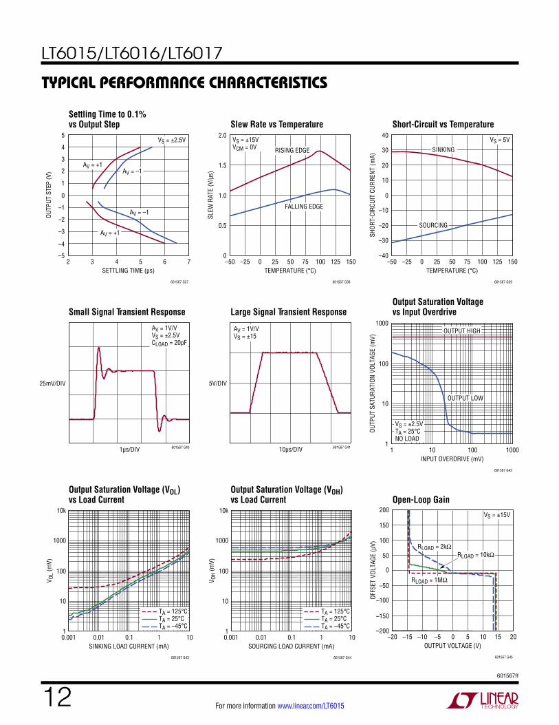
Settling Time to 0.1% vs Output Step Slew Rate vs Temperature Short-Circuit vs Temperature
SETTLING TIME (µs)2
–5
OUTP
UT S
TEP
(V)
5
4
0
–2
–3
–4
3
2
1
–1
3 4 5 6 7
601567 G37
AV = +1AV = –1
AV = –1
AV = +1
VS = ±2.5V
TEMPERATURE (°C)–50
0
SLEW
RAT
E (V
/µs)
2.0
1.0
0.5
1.5
–25 0 25 50 75 100 125 150
601567 G38
VS = ±15VVCM = 0V RISING EDGE
FALLING EDGE
TEMPERATURE (°C)–50
–40
SHOR
T-CI
RCUI
T CU
RREN
T (m
A)
40
0
30
10
–10
–30
–20
20
–25 0 25 50 75 100 125 150
601567 G39
VS = 5V
SINKING
SOURCING
25mV/DIV
1µs/DIV 601567 G40
AV = 1V/VVS = ±2.5VCLOAD = 20pF
INPUT OVERDRIVE (mV)
1
OUTP
UT S
ATUR
ATIO
N VO
LTAG
E (m
V)
1000
100
10
1 10 100 1000
601567 G42
OUTPUT HIGH
OUTPUT LOW
VS = ±2.5VTA = 25°CNO LOAD
OUTPUT VOLTAGE (V)–20
–200
OFFS
ET V
OLTA
GE (µ
V)
200
150
100
50
0
–50
–100
–150
–10–15 0–5 10 155 20
601567 G45
VS = ±15V
RLOAD = 2kΩ
RLOAD = 1MΩ
RLOAD = 10kΩ
SINKING LOAD CURRENT (mA)0.0011
V OL
(mV)
10k
1000
100
10
0.01 0.1 1 10
601567 G43
TA = 125°CTA = 25°CTA = –45°C
SOURCING LOAD CURRENT (mA)0.0011
V OH
(mV)
10k
1000
100
10
0.01 0.1 1 10
601567 G44
TA = 125°CTA = 25°CTA = –45°C
5V/DIV
10µs/DIV 601567 G41
AV = 1V/VVS = ±15
LT6015/LT6016/LT6017
13601567ff
For more information www.linear.com/LT6015
applicaTions inForMaTionSupply Voltage
The positive supply pin of the LT6015/LT6016/LT6017 should be bypassed with a small capacitor (typically 0.1μF) as close to the supply pins as possible. When driving heavy loads an additional 4.7μF electrolytic capacitor should be added. When using split supplies, the same is true for the V– supply pin.
The LT6017 consists of two dual amplifier dice assembled in a single DFN package which share a common substrate (V–). While the V– pins of the quad (pins 16 and 18) must always be tied together and to the exposed pad underneath, the V+ power supply pins (pins 5 and 7) may be supplied independently. The B and C channel amplifiers are supplied through V+ by pin 7, and the A and D channel amplifiers are supplied by pin 5. If pin 5 and pin 7 are not tied together and are biased independently, each V+ pin should have their own dedicated supply bypass to ground.
Shutdown
While there are no dedicated shutdown pins for the LT6015/LT6016/LT6017, the amplifiers can effectively be shut down into a low power state by removing V+. In this condition the input bias current is typically less than 1nA with the inputs biased between V– and 76V above V–, and if the inputs are taken below V–, they appear as a diode in series with 1k of resistance. The output may be pulled up to 50V above the V+ power supply in this condition (See Figure 1). Pulling the output pin below V– will produce unlimited current and can damage the part.
Reverse Battery
The LT6015/LT6016/LT6017 are protected against reverse battery voltages up to 50V. In the event a reverse battery condition occurs, the supply current is typically less than 5µA (assuming the inputs are biased within a diode drop from V–). For typical single supply applications with ground referred loads and feedback networks, no other precautions are required. If the reverse battery condition results in a negative voltage at the input pins, the current into the pin should be limited by an external resistor to less than 10mA.
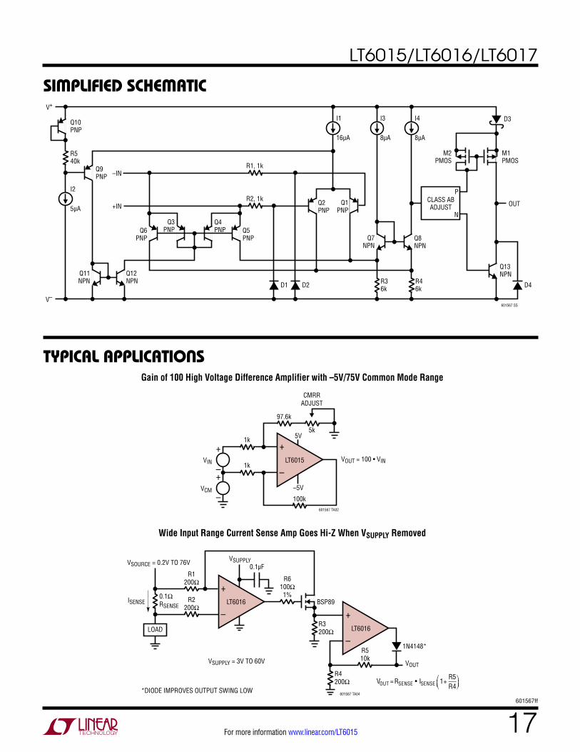
Inputs
Referring to the Simplified Schematic, the LT6015/LT6016/LT6017 has two input stages: a common emitter differential input stage consisting of PNP transistors Q1 and Q2 which operate when the inputs are biased between V– and 1.5V below V+, and a common base input stage consisting of PNP transistors Q3 to Q6 which operate when the common mode input is biased greater than V+ –1.5V. This results in two distinct operating regions as shown in Figure 2.
For common mode input voltages approximately 1.5V or more below the V+ supply (Q1 and Q2 active), the com-mon emitter PNP input stage is active and the input bias current is typically under ±2nA. When the common mode input is within approximately 1V of the V+ supply or higher
Figure 1. LT6015/LT6016/LT6017 Fault Tolerant Conditions
INPUTS DRIVEN ABOVESUPPLY TOLERANT
5V
–
+OK!
80V+
REVERSE BATTERYTOLERANT
–50V
–
+OK!
INPUTS DRIVEN BELOWGROUND TOLERANT
25VTRANSIENT
5V
–
+OK!
LARGE DIFFERENTIALINPUT VOLTAGETOLERANT
5V
–
+OK!
80V+
OUTPUT DRIVEN ABOVE THEV+ SUPPLY (IN SHUTDOWN)TOLERANT
0V
–
+OK!
601567 F01
50V+
–
+
LT6015/LT6016/LT6017
14601567ff
For more information www.linear.com/LT6015
applicaTions inForMaTion(Over-The-Top operation), Q9 begins to turn on diverting bias current away from the common emitter differential input pair to the current mirror consisting of Q11 and Q12. The current from Q12 will bias the common base differential input pair consisting of Q3 to Q6. Because the Over-The-Top input pair is operating in a common base configuration, the input bias current will increase to about 14μA. Both input stages have their voltage offsets trimmed tightly and are specified in the Electrical Characteristics table.
The inputs are protected against temporary excursions to as much as 25V below V– by internal 1k resistor in series with each input and a diode from the input to the negative supply. Adding additional external series resistance will extend the protection beyond 25V below V–. The input stage of the LT6015/LT6016/LT6017 incorporates phase reversal protection to prevent the output from phase reversing for inputs below V–.
There are no clamping diodes between the inputs. The inputs may be over-driven differentially to 80V without damage, or without drawing appreciable input current. Figure 1 summarizes the kind of faults that may be applied to the LT6015/LT6016/LT6017 without damage.
Over-The-Top Operation Considerations
When the input common mode of the LT6015/LT6016/LT6017 is biased near or above the V+ supply, the amplifier is said to be operating in the Over-The-Top configuration. The differential input pair which control amplifier operation is common base pair Q3 to Q6 (refer to the Simplified Schematic). If the input common mode is biased between V– and approximately 1.5V below V+, the amplifier is said to be operating in the normal configuration. The differential input pair which control amplifier operation is common emitter pair Q1 and Q2.
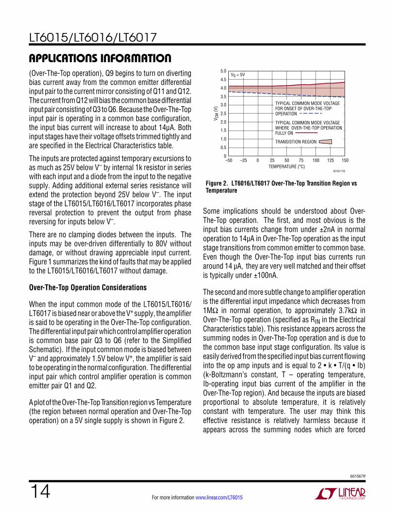
A plot of the Over-The-Top Transition region vs Temperature (the region between normal operation and Over-The-Top operation) on a 5V single supply is shown in Figure 2.
Some implications should be understood about Over-The-Top operation. The first, and most obvious is the input bias currents change from under ±2nA in normal operation to 14µA in Over-The-Top operation as the input stage transitions from common emitter to common base. Even though the Over-The-Top input bias currents run around 14 µA, they are very well matched and their offset is typically under ±100nA.
The second and more subtle change to amplifier operation is the differential input impedance which decreases from 1MΩ in normal operation, to approximately 3.7kΩ in Over-The-Top operation (specified as RIN in the Electrical Characteristics table). This resistance appears across the summing nodes in Over-The-Top operation and is due to the common base input stage configuration. Its value is easily derived from the specified input bias current flowing into the op amp inputs and is equal to 2 • k • T/(q • Ib) (k-Boltzmann’s constant, T – operating temperature, Ib-operating input bias current of the amplifier in the Over-The-Top region). And because the inputs are biased proportional to absolute temperature, it is relatively constant with temperature. The user may think this effective resistance is relatively harmless because it appears across the summing nodes which are forced
Figure 2. LT6016/LT6017 Over-The-Top Transition Region vs Temperature
TEMPERATURE (°C)–50
V CM
(V)
5.0
4.5
3.5
2.5
4.0
3.0
2.0
1.5
1.0
0.5
0500 100 125
601567 F02
15025–25 75
VS = 5V
TRANSISTION REGION
TYPICAL COMMON MODE VOLTAGEFOR ONSET OF OVER-THE-TOPOPERATION
TYPICAL COMMON MODE VOLTAGEWHERE OVER-THE-TOP OPERATIONFULLY ON
LT6015/LT6016/LT6017
15601567ff
For more information www.linear.com/LT6015
to 0V differential by feedback action of the amplifier. However, depending on the configuration of the feedback around the amplifier, this input resistance can boost noise gain, lower overall amplifier loop gain and closed loop bandwidth, raise output noise, with one benevolent effect in increasing amplifier stability.
In the normal mode of operation (where V– < VCM < V+
–1.5V), RIN is typically large compared to the value of the input resistor used, and RIN can be ignored (refer to Figure 3). In this case the noise gain is defined by the equation:
NOISEGAIN ≈ 1+ RF
RI
However, when the amplifier transitions into Over-The-Top mode with the input common mode biased near or above the the V+ supply, RIN should be considered. The noise gain of the amplifier changes to:
NOISEGAIN = 1+ RFRI|| RIN +RI||RF( )
Likewise the closed loop bandwidth of the amplifier will change going from normal mode operation to Over-The-Top operation:
Normal mode:
BWCLOSED − LOOP ≈GBW
1+ RFRI
Over-The-Top mode:
BWCLOSED − LOOP ≈GBW
1+ RFRI|| RIN +RI||RF( )
And output noise is negatively impacted going from normal mode to Over-The-Top:
Normal mode: (neglecting resistor noise)
eno ≈ eni • 1+ RF
RI
⎛⎝⎜
⎞⎠⎟
Over-The-Top mode: (neglecting resistor noise)
eno ≈ eni • 1+ RF
RI|| RIN +RI||RF( )⎛
⎝⎜⎞
⎠⎟
Output
The output of the LT6015/LT6016/LT6017 can swing within a Schottky diode drop (~0.4V) of the V+ supply, and within 5mV of the negative supply with no load. The output is capable of sourcing and sinking approximately 25mA.
The LT6015/LT6016/LT6017 are internally compensated to drive at least 200pF of capacitance under any output loading conditions. For larger capacitive loads, a 0.22μF capacitor in series with a 150Ω resistor between the out-put and ground will compensate these amplifiers to drive capacitive loads greater than 200pF.
applicaTions inForMaTion
While it is true that the DC closed loop gain will remain mostly unaffected (= RF
RI ), the loop gain of the amplifier
has decreased from
AOL
1+ RFRI
to
AOL
1+ RFRI|| RIN +RI||RF( )
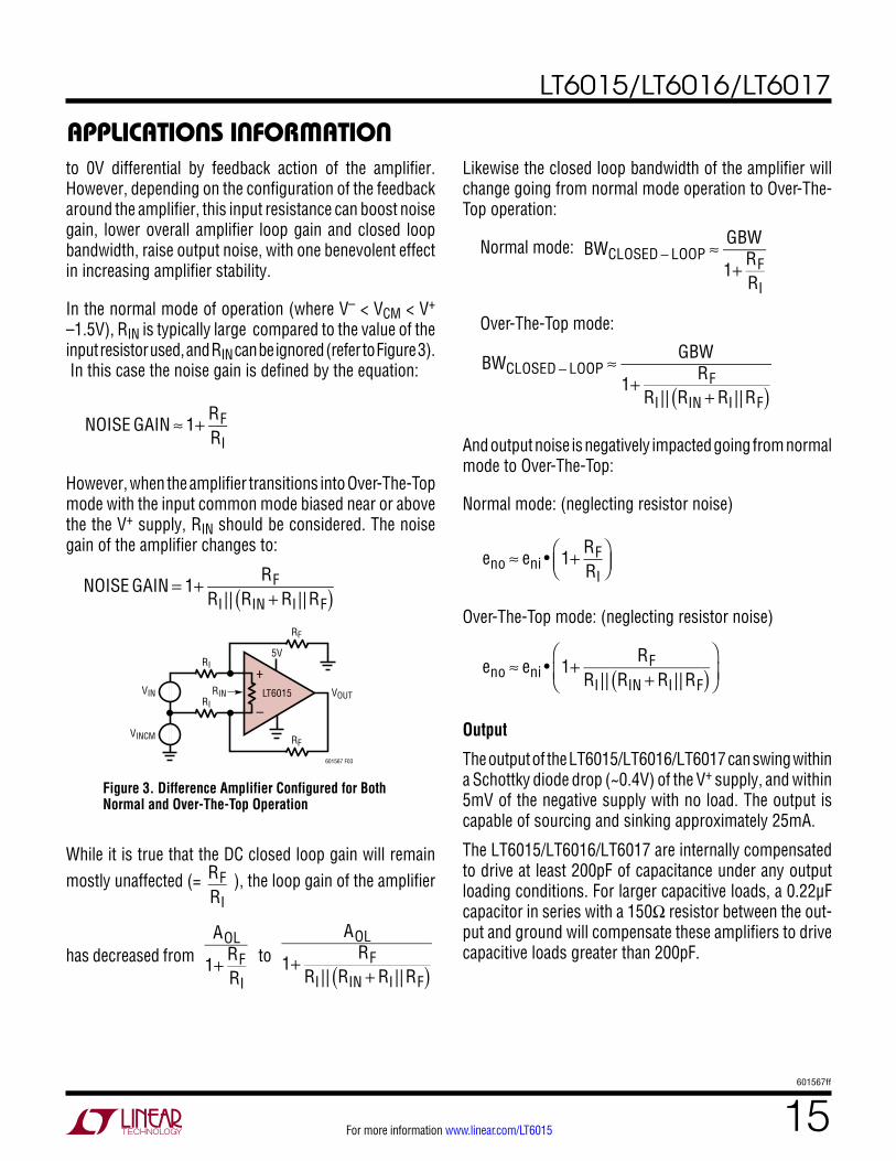
Figure 3. Difference Amplifier Configured for Both Normal and Over-The-Top Operation
+
–
5V
LT6015VIN
VINCM
RI
RF
VOUT
RF
RIRIN
601567 F03
LT6015/LT6016/LT6017
16601567ff
For more information www.linear.com/LT6015
Distortion
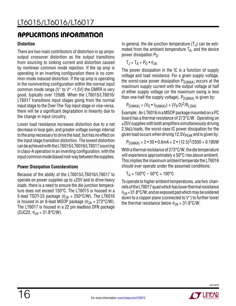
There are two main contributors of distortion in op amps: output crossover distortion as the output transitions from sourcing to sinking current and distortion caused by nonlinear common mode rejection. If the op amp is operating in an inverting configuration there is no com-mon mode induced distortion. If the op amp is operating in the noninverting configuration within the normal input common mode range (V– to V+ –1.5V) the CMRR is very good, typically over 120dB. When the LT6015/LT6016/LT6017 transitions input stages going from the normal input stage to the Over-The-Top input stage or vice-versa, there will be a significant degradation in linearity due to the change in input circuitry.
Lower load resistance increases distortion due to a net decrease in loop gain, and greater voltage swings internal to the amp necessary to drive the load, but has no effect on the input stage transition distortion. The lowest distortion can be achieved with the LT6015/LT6016/LT6017 sourcing in class-A operation in an inverting configuration, with the input common mode biased mid-way between the supplies.
Power Dissipation Considerations
Because of the ability of the LT6015/LT6016/LT6017 to operate on power supplies up to ±25V and to drive heavy loads, there is a need to ensure the die junction tempera-ture does not exceed 150°C. The LT6015 is housed in a 5-lead TSOT-23 package (JA = 250°C/W). The LT6016 is housed in an 8-lead MSOP package (JA = 273°C/W). The LT6017 is housed in a 22 pin leadless DFN package (DJC22, JA = 31.8°C/W).
In general, the die junction temperature (TJ) can be esti-mated from the ambient temperature TA, and the device power dissipation PD:
TJ = TA + PD • JA
The power dissipation in the IC is a function of supply voltage and load resistance. For a given supply voltage, the worst-case power dissipation PD(MAX) occurs at the maximum supply current with the output voltage at half of either supply voltage (or the maximum swing is less than one-half the supply voltage). PD(MAX) is given by:
PD(MAX) = (VS • IS(MAX)) + (VS/2)2/RLOAD
Example: An LT6016 in a MSOP package mounted on a PC board has a thermal resistance of 273°C/W. Operating on ±25V supplies with both amplifiers simultaneously driving 2.5kΩ loads, the worst-case IC power dissipation for the given load occurs when driving 12.5VPEAK and is given by:
PD(MAX) = 2 • 50 • 0.6mA + 2 • (12.5)2/2500 = 0.185W
With a thermal resistance of 273°C/W, the die temperature will experience approximately a 50°C rise above ambient. This implies the maximum ambient temperate the LT6016 should ever operate under the assumed conditions:
TA = 150°C – 50°C = 100°C
To operate to higher ambient temperatures, use two chan-nels of the LT6017 quad which has lower thermal resistance JA = 31.8°C/W, and an exposed pad which may be soldered down to a copper plane (connected to V–) to further lower the thermal resistance below JA = 31.8°C/W.
applicaTions inForMaTion
LT6015/LT6016/LT6017
17601567ff
For more information www.linear.com/LT6015
siMpliFieD scheMaTic
601567 SS
Q10PNP
Q9PNP
Q6PNP
Q5PNP
Q2PNP
Q1PNP
Q3PNP
Q4PNP
Q12NPN
Q11NPN
R540k
5µA
I2
V+
V–
–IN
R36k
R46k
+IN
D4D1 D2
R1, 1k
R2, 1k
16µA
I1
8µA
I3
8µA
OUT
M2PMOS
M1PMOS
I4
Q7NPN
Q8NPN
Q13NPN
P
N
CLASS ABADJUST
D3
Typical applicaTionsGain of 100 High Voltage Difference Amplifier with –5V/75V Common Mode Range
Wide Input Range Current Sense Amp Goes Hi-Z When VSUPPLY Removed
–
+5V
–5V
1k
100k
97.6k
CMRRADJUST
5k
1kVOUT = 100 • VINLT6015VIN
VCM
601567 TA02
+
–+
–
–
+
R1200Ω R6
100Ω1%
R510k
R3200Ω
R4200Ω
R2200Ω
0.1µF
0.1ΩRSENSE
BSP89
*DIODE IMPROVES OUTPUT SWING LOW
1N4148*
LT6016
VSOURCE = 0.2V TO 76V
VSUPPLY = 3V TO 60V VOUT
ISENSE
VSUPPLY
601567 TA04
LOAD
–
+LT6016
VOUT =RSENSE • ISENSE 1+
R5R4
⎛⎝⎜
⎞⎠⎟
LT6015/LT6016/LT6017
18601567ff
For more information www.linear.com/LT6015
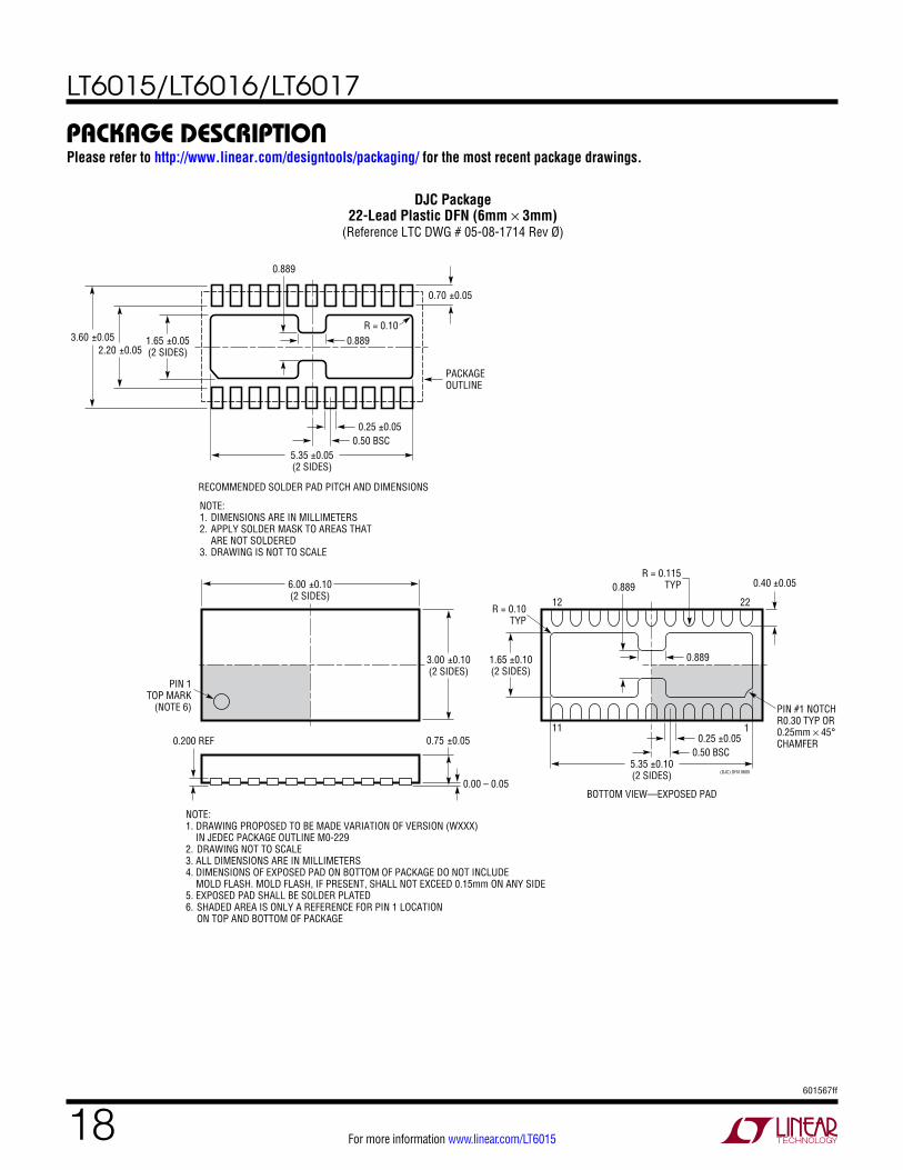
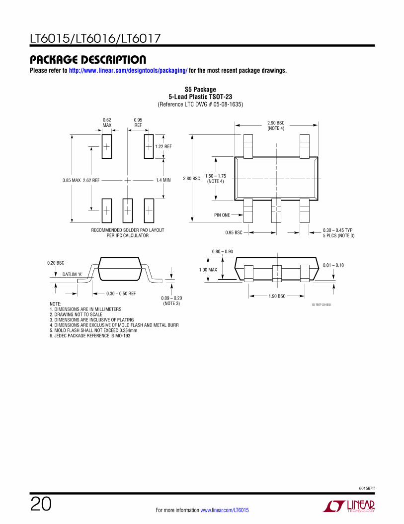
package DescripTionPlease refer to http://www.linear.com/designtools/packaging/ for the most recent package drawings.
3.00 ±0.10(2 SIDES)
NOTE:1. DRAWING PROPOSED TO BE MADE VARIATION OF VERSION (WXXX) IN JEDEC PACKAGE OUTLINE M0-2292. DRAWING NOT TO SCALE3. ALL DIMENSIONS ARE IN MILLIMETERS4. DIMENSIONS OF EXPOSED PAD ON BOTTOM OF PACKAGE DO NOT INCLUDE MOLD FLASH. MOLD FLASH, IF PRESENT, SHALL NOT EXCEED 0.15mm ON ANY SIDE5. EXPOSED PAD SHALL BE SOLDER PLATED6. SHADED AREA IS ONLY A REFERENCE FOR PIN 1 LOCATION ON TOP AND BOTTOM OF PACKAGE
NOTE:1. DIMENSIONS ARE IN MILLIMETERS2. APPLY SOLDER MASK TO AREAS THAT ARE NOT SOLDERED3. DRAWING IS NOT TO SCALE
0.40 ±0.05
PIN #1 NOTCHR0.30 TYP OR0.25mm × 45°CHAMFER
BOTTOM VIEW—EXPOSED PAD
1.65 ±0.10(2 SIDES)
0.75 ±0.05
R = 0.115TYP
R = 0.10TYP
1
2212
11
PIN 1TOP MARK
(NOTE 6)
0.200 REF
0.00 – 0.05(DJC) DFN 0605
6.00 ±0.10(2 SIDES)
0.25 ±0.05
0.889
0.889
0.50 BSC5.35 ±0.10(2 SIDES)
R = 0.10
RECOMMENDED SOLDER PAD PITCH AND DIMENSIONS
1.65 ±0.05(2 SIDES)2.20 ±0.05
0.70 ±0.05
3.60 ±0.05
PACKAGEOUTLINE
0.25 ±0.050.50 BSC
5.35 ±0.05(2 SIDES)
0.889
0.889
DJC Package22-Lead Plastic DFN (6mm × 3mm)
(Reference LTC DWG # 05-08-1714 Rev Ø)
LT6015/LT6016/LT6017
19601567ff
For more information www.linear.com/LT6015
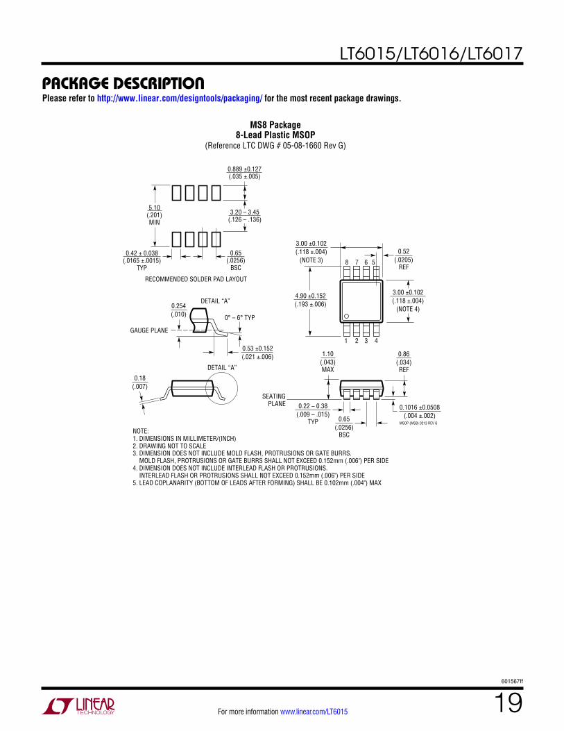
package DescripTionPlease refer to http://www.linear.com/designtools/packaging/ for the most recent package drawings.
MSOP (MS8) 0213 REV G
0.53 ±0.152(.021 ±.006)
SEATINGPLANE
NOTE:1. DIMENSIONS IN MILLIMETER/(INCH)2. DRAWING NOT TO SCALE3. DIMENSION DOES NOT INCLUDE MOLD FLASH, PROTRUSIONS OR GATE BURRS. MOLD FLASH, PROTRUSIONS OR GATE BURRS SHALL NOT EXCEED 0.152mm (.006") PER SIDE4. DIMENSION DOES NOT INCLUDE INTERLEAD FLASH OR PROTRUSIONS. INTERLEAD FLASH OR PROTRUSIONS SHALL NOT EXCEED 0.152mm (.006") PER SIDE5. LEAD COPLANARITY (BOTTOM OF LEADS AFTER FORMING) SHALL BE 0.102mm (.004") MAX
0.18(.007)
0.254(.010)
1.10(.043)MAX
0.22 – 0.38(.009 – .015)
TYP
0.1016 ±0.0508(.004 ±.002)
0.86(.034)REF
0.65(.0256)
BSC
0° – 6° TYP
DETAIL “A”
DETAIL “A”
GAUGE PLANE
1 2 3 4
4.90 ±0.152(.193 ±.006)
8 7 6 5
3.00 ±0.102(.118 ±.004)
(NOTE 3)
3.00 ±0.102(.118 ±.004)
(NOTE 4)
0.52(.0205)
REF
5.10(.201)MIN
3.20 – 3.45(.126 – .136)
0.889 ±0.127(.035 ±.005)
RECOMMENDED SOLDER PAD LAYOUT
0.42 ± 0.038(.0165 ±.0015)
TYP
0.65(.0256)
BSC
MS8 Package8-Lead Plastic MSOP
(Reference LTC DWG # 05-08-1660 Rev G)
LT6015/LT6016/LT6017
20601567ff
For more information www.linear.com/LT6015
package DescripTionPlease refer to http://www.linear.com/designtools/packaging/ for the most recent package drawings.
1.50 – 1.75(NOTE 4)2.80 BSC
0.30 – 0.45 TYP 5 PLCS (NOTE 3)
DATUM ‘A’
0.09 – 0.20(NOTE 3) S5 TSOT-23 0302
PIN ONE
2.90 BSC(NOTE 4)
0.95 BSC
1.90 BSC
0.80 – 0.90
1.00 MAX0.01 – 0.100.20 BSC
0.30 – 0.50 REF
NOTE:1. DIMENSIONS ARE IN MILLIMETERS2. DRAWING NOT TO SCALE3. DIMENSIONS ARE INCLUSIVE OF PLATING4. DIMENSIONS ARE EXCLUSIVE OF MOLD FLASH AND METAL BURR5. MOLD FLASH SHALL NOT EXCEED 0.254mm6. JEDEC PACKAGE REFERENCE IS MO-193
3.85 MAX
0.62MAX
0.95REF
RECOMMENDED SOLDER PAD LAYOUTPER IPC CALCULATOR
1.4 MIN2.62 REF
1.22 REF
S5 Package5-Lead Plastic TSOT-23
(Reference LTC DWG # 05-08-1635)
LT6015/LT6016/LT6017
21601567ff
For more information www.linear.com/LT6015Information furnished by Linear Technology Corporation is believed to be accurate and reliable. However, no responsibility is assumed for its use. Linear Technology Corporation makes no representa-tion that the interconnection of its circuits as described herein will not infringe on existing patent rights.
revision hisToryREV DATE DESCRIPTION PAGE NUMBER
A 01/13 Corrected Block Diagram Q7 and Q8 17
B 06/13 Added LT6015 Single AmplifierChanged MIN IB at VCM = 0V to –60nA, changed GBW test condition to fTEST = 100kHzAdded Wide Input Range Current Sense Amp circuit
All3-717
C 11/13 Revised Order Information table to include mini tape and reel for LT6015 2
D 12/13 Corrected quad pinout 2, 13
E 09/14 Corrected TSOT-23 part marking and package description 2
F 08/15 Corrected axis label on graph G32 11
LT6015/LT6016/LT6017
22601567ff
For more information www.linear.com/LT6015© LINEAR TECHNOLOGY CORPORATION 2012
LT 0915 REV F • PRINTED IN USALinear Technology Corporation1630 McCarthy Blvd., Milpitas, CA 95035-7417(408) 432-1900 ● FAX: (408) 434-0507 ● www.linear.com/LT6015
relaTeD parTs
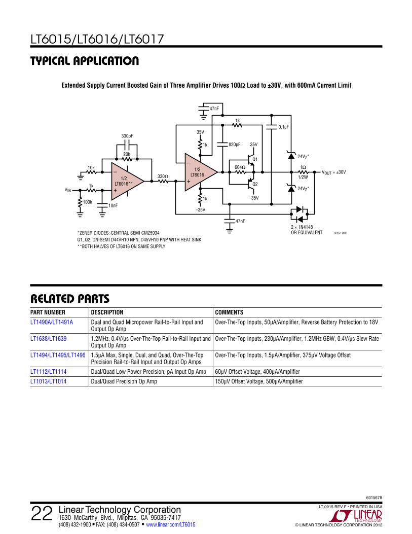
Typical applicaTion
PART NUMBER DESCRIPTION COMMENTS
LT1490A/LT1491A Dual and Quad Micropower Rail-to-Rail Input and Output Op Amp
Over-The-Top Inputs, 50μA/Amplifier, Reverse Battery Protection to 18V
LT1638/LT1639 1.2MHz, 0.4V/µs Over-The-Top Rail-to-Rail Input and Output Op Amp
Over-The-Top Inputs, 230μA/Amplifier, 1.2MHz GBW, 0.4V/µs Slew Rate
LT1494/LT1495/LT1496 1.5μA Max, Single, Dual, and Quad, Over-The-Top Precision Rail-to-Rail Input and Output Op Amps
Over-The-Top Inputs, 1.5μA/Amplifier, 375μV Voltage Offset
LT1112/LT1114 Dual/Quad Low Power Precision, pA Input Op Amp 60μV Offset Voltage, 400μA/Amplifier
LT1013/LT1014 Dual/Quad Precision Op Amp 150μV Offset Voltage, 500μA/Amplifier
Extended Supply Current Boosted Gain of Three Amplifier Drives 100Ω Load to ±30V, with 600mA Current Limit
–
+
35V
–35V
1k
604Ω 1Ω
1/2W
1k 820pF 35V
–35V
1k0.1µF
1/2LT6016 VOUT = ±30V
24VZ*
24VZ*
2 × 1N4148OR EQUIVALENT 60167 TA03
47nF
Q1
Q2
47nF
10nF
*ZENER DIODES: CENTRAL SEMI CMZ5934Q1, Q2: ON-SEMI D44VH10 NPN, D45VH10 PNP WITH HEAT SINK**BOTH HALVES OF LT6016 ON SAME SUPPLY
–
+
1/2LT6016**
330Ω
10k
VIN1k
20k
100k
330pF
Related Documents