LT3964 1 For more information www.linear.com/LT3964 3964fb TYPICAL APPLICATION FEATURES DESCRIPTION Dual 36V Synchronous 1.6A Buck LED Driver with I 2 C The LT ® 3964 is a dual synchronous step-down DC/DC converter with I 2 C interface designed to operate as a constant-current and constant-voltage source and is ideal for driving LEDs. The fixed frequency and peak current mode topology result in stable operation over a wide range of supply and output voltages. The ground referred volt- age FB pin serves as the input for several LED protection features, and also allows the converter to operate as a constant-voltage source. The maximum output current is set by an external resistor, and the output current ampli- fier has a rail-to-rail common mode range. LT3964 uses an I 2 C interface to communicate with a microcontroller to read LED faults, write PWM and analog dimming reg- isters and set fault masking. The I 2 C PWM input provides LED dimming ratios up to 8192:1. The I 2 C programmable CTRL register sets the gain of the external CTRL pin, and maximum current sense threshold, providing additional analog dimming capability. 50W Dual Buck 1A LED Driver APPLICATIONS n Wide Input Voltage Range: 4V to 36V n Two Independent 1.6A/40V Synchronous Bucks n I 2 C Interface for Internal True Color PWM™ Dimming (8192:1), Analog Dimming and Fault Reporting n 1000:1 External True Color PWM Dimming and 10:1 External Analog Dimming n PMOS Switch Driver for PWM and Output Disconnect n ±3% Constant Current Regulation n Adjustable Frequency: 200kHz to 2MHz n Frequency Synchronization with Clock Output n Programmable OPENLED Protection with Reporting n Short-Circuit Protection with Reporting n Programmable Undervoltage Lockout with Hysteresis n Internal Compensation n 9 Unique Device Addresses for I 2 C n Available in 5mm × 6mm 36-Lead QFN Package n General Purpose, Industrial, Medical and Automotive Lighting n Constant-Current, Constant-Voltage Source All registered trademarks and trademarks are the property of their respective owners. Protected by U.S. Patents, including 7199560, 7321203, 7746300. Efficiency, V IN = 34V I LED (mA) 100 200 300 400 500 600 700 800 900 1000 70 75 80 85 90 95 100 EFFICIENCY (%) 3964 TA01b BOTH CHANNELS ARE ON 10μH 0.22μF 1M 100mΩ 2.2μF 43.2k 2.2μF 100k 3.92k 499k 165k 100k 2.2μF 27.4k 2.2μF BST1 LT3964 SW1 V IN1 ISP1 ISN1 PWMTG1 CTRL1 BST2 SW2 ISP2 ISN2 PWMTG2 GND EN/UVLO CTRL2 PWM1 PWM2 PWM1 PWM2 INTV CC ALERT V IN2 GND T SET RT SCL SDA 2-WIRE I 2 C INTERFACE ADDR1 ADDR2 SYNC/CLKOUT 2MHz INTV CC INTV CC INTV CC FB1 FB2 10μH 0.22μF 1M 100mΩ 2.2μF 43.2k 1A, 8 LEDs UP TO 26V 1A, 8 LEDs UP TO 26V 10μF ×2 31V TO 36V (ENABLED AT 33V, SHUTDOWN AT 31V) 3964 TA01a

Welcome message from author
This document is posted to help you gain knowledge. Please leave a comment to let me know what you think about it! Share it to your friends and learn new things together.
Transcript

LT3964
1For more information www.linear.com/LT3964
3964fb
TYPICAL APPLICATION
FEATURES DESCRIPTION
Dual 36V Synchronous 1.6A Buck LED Driver with I2C
The LT®3964 is a dual synchronous step-down DC/DC converter with I2C interface designed to operate as a constant-current and constant-voltage source and is ideal for driving LEDs. The fixed frequency and peak current mode topology result in stable operation over a wide range of supply and output voltages. The ground referred volt-age FB pin serves as the input for several LED protection features, and also allows the converter to operate as a constant-voltage source. The maximum output current is set by an external resistor, and the output current ampli-fier has a rail-to-rail common mode range. LT3964 uses an I2C interface to communicate with a microcontroller to read LED faults, write PWM and analog dimming reg-isters and set fault masking. The I2C PWM input provides LED dimming ratios up to 8192:1. The I2C programmable CTRL register sets the gain of the external CTRL pin, and maximum current sense threshold, providing additional analog dimming capability.
50W Dual Buck 1A LED Driver
APPLICATIONS
n Wide Input Voltage Range: 4V to 36V n Two Independent 1.6A/40V Synchronous Bucks n I2C Interface for Internal True Color PWM™ Dimming
(8192:1), Analog Dimming and Fault Reporting n 1000:1 External True Color PWM Dimming and
10:1 External Analog Dimming n PMOS Switch Driver for PWM and Output Disconnect n ±3% Constant Current Regulation n Adjustable Frequency: 200kHz to 2MHz n Frequency Synchronization with Clock Output n Programmable OPENLED Protection with Reporting n Short-Circuit Protection with Reporting n Programmable Undervoltage Lockout with Hysteresis n Internal Compensation n 9 Unique Device Addresses for I2C n Available in 5mm × 6mm 36-Lead QFN Package
n General Purpose, Industrial, Medical and Automotive Lighting
n Constant-Current, Constant-Voltage Source
All registered trademarks and trademarks are the property of their respective owners. Protected by U.S. Patents, including 7199560, 7321203, 7746300.
Efficiency, VIN = 34V
ILED (mA)100 200 300 400 500 600 700 800 900 1000
70
75
80
85
90
95
100
EFFI
CIEN
CY (%
)
IN
3964 TA01b
BOTH CHANNELS ARE ON
10µH0.22µF
1M
100mΩ
2.2µF
43.2k
2.2µF
100k
3.92k
499k
165k
100k2.2µF
27.4k
2.2µF
BST1
LT3964
SW1
VIN1
ISP1ISN1
PWMTG1
CTRL1
BST2
SW2
ISP2ISN2
PWMTG2
GND
EN/UVLO
CTRL2
PWM1PWM2
PWM1PWM2
INTVCC
ALERT
VIN2
GND
TSETRT
SCLSDA
2-WIREI2C INTERFACE
ADDR1 ADDR2
SYNC/CLKOUT2MHz
INTVCC
INTVCC
INTVCC
FB1
FB2
10µH0.22µF
1M
100mΩ
2.2µF
43.2k
1A, 8 LEDsUP TO26V
1A, 8 LEDsUP TO26V
10µF×2
31V TO 36V(ENABLED AT 33V,
SHUTDOWN AT 31V)
3964 TA01a

LT3964
2 For more information www.linear.com/LT3964
3964fb
PIN CONFIGURATIONABSOLUTE MAXIMUM RATINGS
VIN1, VIN2, EN/UVLO .................................................40VISP1, ISN1, ISP2, ISN2 ..............................................40VPWMTG1, PWMTG2, RT .......................................Note 2SW1, SW2 .................................................................40VBST1, BST2 ............................................................44.5VBST1 to SW1, BST2 to SW2 ....................................4.5VFB1, FB2, CTRL1, CTRL2, ADDR1, ADDR2 ..................5VSYNC/CLKOUT, PWM1, PWM2, TSET ..........................6VSDA, SCL, ALERT ........................................................6VINTVCC ..................................................................Note 3Operating Junction Temperature (Notes 4, 5) LT3964E/LT3964I .............................. –40°C to 125°C LT3964H ............................................ –40°C to 150°CStorage Temperature Range .................. –60°C to 150°C
(Note 1)
11 12 13 14
TOP VIEW
37PGND
UHE PACKAGE36-LEAD (5mm × 6mm) PLASTIC QFN
15 16 17 18
36 35 34 33 32 31 30 29
21
22
23
24
25
26
27
28
8
7
6
5
4
3
2
1RT
CTRL1
CTRL2
EN/UVLO
INTVCC
ALERT
PWM1
PWM2
SDA
SCL
ISP1
ISN1
PWMTG1
SGND
FB1
FB2
SGND
PWMTG2
ISN2
ISP2
SYNC
/CLK
OUT
T SET
V IN1
V IN1
NC SW1
SW1
BST1
ADDR
2
ADDR
1
V IN2
V IN2 NC
SW2
SW2
BST2
20
19
9
10
θJA = 43°C/W, θJC = 5°C/W
EXPOSED PAD (PIN 37) IS PGND, MUST BE SOLDERED TO PCB
ORDER INFORMATIONLEAD FREE FINISH TAPE AND REEL PART MARKING PACKAGE DESCRIPTION TEMPERATURE RANGE
LT3964EUHE#PBF LT3964EUHE#TRPBF 3964 36-Lead (5mm × 6mm) Plastic QFN –40°C to 125°C
LT3964IUHE#PBF LT3964IUHE#TRPBF 3964 36-Lead (5mm × 6mm) Plastic QFN –40°C to 125°C
LT3964HUHE#PBF LT3964HUHE#TRPBF 3964 36-Lead (5mm × 6mm) Plastic QFN –40°C to 150°C
Consult ADI Marketing for parts specified with wider operating temperature ranges.For more information on lead free part marking, go to: http://www.linear.com/leadfree/ For more information on tape and reel specifications, go to: http://www.linear.com/tapeandreel/. Some packages are available in 500 unit reels through designated sales channels with #TRMPBF suffix.
http://www.linear.com/product/LT3964#orderinfo
LT3964
3For more information www.linear.com/LT3964
3964fb
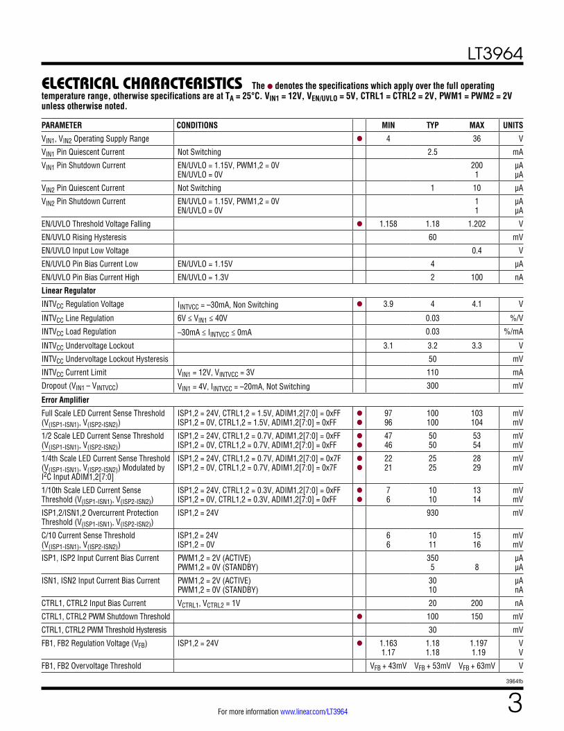
ELECTRICAL CHARACTERISTICS The l denotes the specifications which apply over the full operating temperature range, otherwise specifications are at TA = 25°C. VIN1 = 12V, VEN/UVLO = 5V, CTRL1 = CTRL2 = 2V, PWM1 = PWM2 = 2V unless otherwise noted.
PARAMETER CONDITIONS MIN TYP MAX UNITS
VIN1, VIN2 Operating Supply Range l 4 36 V
VIN1 Pin Quiescent Current Not Switching 2.5 mA
VIN1 Pin Shutdown Current EN/UVLO = 1.15V, PWM1,2 = 0V EN/UVLO = 0V
200 1
µA µA
VIN2 Pin Quiescent Current Not Switching 1 10 µA
VIN2 Pin Shutdown Current EN/UVLO = 1.15V, PWM1,2 = 0V EN/UVLO = 0V
1 1
µA µA
EN/UVLO Threshold Voltage Falling l 1.158 1.18 1.202 V
EN/UVLO Rising Hysteresis 60 mV
EN/UVLO Input Low Voltage 0.4 V
EN/UVLO Pin Bias Current Low EN/UVLO = 1.15V 4 µA
EN/UVLO Pin Bias Current High EN/UVLO = 1.3V 2 100 nA
Linear Regulator
INTVCC Regulation Voltage IINTVCC = –30mA, Non Switching l 3.9 4 4.1 V
INTVCC Line Regulation 6V ≤ VIN1 ≤ 40V 0.03 %/V
INTVCC Load Regulation –30mA ≤ IINTVCC ≤ 0mA 0.03 %/mA
INTVCC Undervoltage Lockout 3.1 3.2 3.3 V
INTVCC Undervoltage Lockout Hysteresis 50 mV
INTVCC Current Limit VIN1 = 12V, VINTVCC = 3V 110 mA
Dropout (VIN1 – VINTVCC) VIN1 = 4V, IINTVCC = –20mA, Not Switching 300 mV
Error Amplifier
Full Scale LED Current Sense Threshold (V(ISP1-ISN1), V(ISP2-ISN2))
ISP1,2 = 24V, CTRL1,2 = 1.5V, ADIM1,2[7:0] = 0xFF ISP1,2 = 0V, CTRL1,2 = 1.5V, ADIM1,2[7:0] = 0xFF
l
l
97 96
100 100
103 104
mV mV
1/2 Scale LED Current Sense Threshold (V(ISP1-ISN1), V(ISP2-ISN2))
ISP1,2 = 24V, CTRL1,2 = 0.7V, ADIM1,2[7:0] = 0xFF ISP1,2 = 0V, CTRL1,2 = 0.7V, ADIM1,2[7:0] = 0xFF
l
l 47 46
50 50
53 54
mV mV
1/4th Scale LED Current Sense Threshold (V(ISP1-ISN1), V(ISP2-ISN2)) Modulated by I2C Input ADIM1,2[7:0]
ISP1,2 = 24V, CTRL1,2 = 0.7V, ADIM1,2[7:0] = 0x7F ISP1,2 = 0V, CTRL1,2 = 0.7V, ADIM1,2[7:0] = 0x7F
l
l
22 21
25 25
28 29
mV mV
1/10th Scale LED Current Sense Threshold (V(ISP1-ISN1), V(ISP2-ISN2))
ISP1,2 = 24V, CTRL1,2 = 0.3V, ADIM1,2[7:0] = 0xFF ISP1,2 = 0V, CTRL1,2 = 0.3V, ADIM1,2[7:0] = 0xFF
l
l
7 6
10 10
13 14
mV mV
ISP1,2/ISN1,2 Overcurrent Protection Threshold (V(ISP1-ISN1), V(ISP2-ISN2))
ISP1,2 = 24V 930 mV
C/10 Current Sense Threshold (V(ISP1-ISN1), V(ISP2-ISN2))
ISP1,2 = 24V ISP1,2 = 0V
6 6
10 11
15 16
mV mV
ISP1, ISP2 Input Current Bias Current PWM1,2 = 2V (ACTIVE) PWM1,2 = 0V (STANDBY)
350 5
8
µA µA
ISN1, ISN2 Input Current Bias Current PWM1,2 = 2V (ACTIVE) PWM1,2 = 0V (STANDBY)
30 10
µA nA
CTRL1, CTRL2 Input Bias Current VCTRL1, VCTRL2 = 1V 20 200 nA
CTRL1, CTRL2 PWM Shutdown Threshold l 100 150 mV
CTRL1, CTRL2 PWM Threshold Hysteresis 30 mV
FB1, FB2 Regulation Voltage (VFB) ISP1,2 = 24V l 1.163 1.17
1.18 1.18
1.197 1.19
V V
FB1, FB2 Overvoltage Threshold VFB + 43mV VFB + 53mV VFB + 63mV V

LT3964
4 For more information www.linear.com/LT3964
3964fb
PARAMETER CONDITIONS MIN TYP MAX UNITS
FB1, FB2 OPENLED Threshold VFB – 43mV VFB – 53mV VFB – 63mV V
FB1, FB2 SHORTLED Threshold l 250 270 mV
FB1, FB2 Pin Input Bias Current Current Out of Pin, FB = 1V 20 200 nA
Feedback Line Regulation 4V ≤ VIN1 ≤ 36V 0.001 %/V
TSET Pin Voltage 630 mV
TSET Pin Bias Current Current Out of Pin, TSET = 400mV 40 200 nA
Oscillator
RT Pin Voltage 0.96 V
Switching Frequency RT = 357k RT = 60.4k RT = 27.4k
l
l
l
186 0.93 1.86
200 1.0 2.0
214 1.07 2.14
kHz MHz MHz
SYNC/CLKOUT Pin Resistance to GND 100 kΩ
SYNC/CLKOUT Input High Threshold 1.5 V
SYNC/CLKOUT Input Low Threshold 0.4 V
SYNC/CLKOUT Output Duty Cycle CONFIG[6] = 1 (Clock Output Enabled) 30 50 70 %
SYNC/CLKOUT Output Voltage High CONFIG[6] = 1 (Clock Output Enabled) 4 V
SYNC/CLKOUT Output Voltage Low CONFIG[6] = 1 (Clock Output Enabled) 0.1 0.3 V
SYNC/CLKOUT Output Rise Time CSYNC/CLKOUT = 50pF, CONFIG[6] = 1 (Clock Output Enabled)
40 ns
SYNC/CLKOUT Output Fall Time CSYNC/CLKOUT = 50pF, CONFIG[6] = 1 (Clock Output Enabled)
20 ns
Logic
ALERT Output Low IALERT = 1mA 300 mV
PWM1, PWM2 Input High Voltage l 1.18 1.3 V
PWM1, PWM2 Input Low Voltage l 1.1 1.15 V
PWM1, PWM2 Resistance to GND 280 kΩ
Power Switch
Top Switch On Resistance ISW = 1A 200 mΩ
Top Switch Current Limit l 1.6 1.8 2 A
Bottom Switch On Resistance ISW = 1A 180 mΩ
Bottom Switch Current Limit 1.6 2 2.4 A
SW Leakage Current VIN = 36V, VSW = 0V, 36V –1.5 1.5 µA
Minimum Off Time 20 50 70 ns
Minimum ON Time 20 40 65 ns
PWMTG Gate Driver
PWMTG ON Voltage (VISP1-PWMTG1, VISP2-PWMTG2)
ISP1,2 = 36V 7.5 9.5 V
PWMTG OFF Voltage (VISP1-PWMTG1, VISP2-PWMTG2)
ISP1,2 = 36V 0 0.3 V
PWMTG Turn-On Time CLOAD = 500pF, ISP1,2 = 36V 70 ns
PWMTG Turn-Off Time CLOAD = 500pF, ISP1,2 = 36V 40 ns
ELECTRICAL CHARACTERISTICS The l denotes the specifications which apply over the full operating temperature range, otherwise specifications are at TA = 25°C. VIN1 = 12V, VEN/UVLO = 5V, CTRL1 = CTRL2 = 2V, PWM1 = PWM2 = 2V unless otherwise noted.

LT3964
5For more information www.linear.com/LT3964
3964fb
PARAMETER CONDITIONS MIN TYP MAX UNITS
I2C Port (Note 6)
I2C Address XXXX Bits Are Programmed by ADDR[1:2] l 110XXXX[R/W]
VIHA High Level Input Voltage for Address Pins ADDR1, ADDR2 l INTVCC – 0.8 V
VILA Low Level Input Voltage for Address Pins ADDR1, ADDR2 l 0.6 V
RINH Resistance from ADDR1, ADDR2 to INTVCC to Set Chip Address Bit to 1
l 10 kΩ
RINL Resistance from ADDR1, ADDR2 to GND to Set Chip Address Bit to 0
l 10 kΩ
RINF Resistance from ADDR1, ADDR2 to GND or INTVCC to Set Chip Address Bit to Float
l 1 MΩ
SDA and SCL Input High Voltage l 1.5 V
SDA and SCL Input Low Voltage l 0.4 V
SDA and SCL Input High Current SDA, SCL = 3.3V 50 nA
SDA and SCL Input Low Current Current Out of Pin, SDA, SCL = 0V 50 nA
SDA Output Low Voltage ISDA = 3mA 0.4 V
Clock Operating Frequency 400 kHz
Bus Free Time Between Stop and Start Condition (tBUF)
1.3 µs
Hold Time After Repeated Start Condition (tHD,SDA)
0.6 µs
Repeated Start Condition Set-Up Time (tSU,STA)
0.6 µs
Stop Condition Set-Up Time (tSU,STO) 0.6 µs
Data Hold Time Output (tHD,DAT(O)) 0 900 ns
Data Hold Time Input (tHD,DAT(I)) 0 ns
Data Set-Up Time (tSU,DAT) 250 ns
SCL Clock Low Period (tLOW) 1.3 µs
SCL Clock High Period (tHIGH) 0.6 µs
Data Fall Time CB = Capacitance of One Bus Line (pF) 20 + 0.1CB 300 ns
Data Rise Time CB = Capacitance of One Bus Line (pF) 20 + 0.1CB 300 ns
Input Spike Suppress Pulse Width (tSP) 50 ns
Note 1: Stresses beyond those listed under Absolute Maximum Ratings may cause permanent damage to the device. Exposure to any Absolute Maximum Rating condition for extended periods may affect device reliability and lifetime. Note 2: Do not apply a positive or negative voltage source to the PWMTG pin or RT pin, otherwise permanent damage may occur. Note 3: Do not apply a positive or negative voltage source to INTVCC pin, otherwise permanent damage may occur. IINTVCC = 5mA is the maximum external load that can be applied. The internal load will be higher due to the power consumption of the IC.Note 4: The LT3964E is guaranteed to meet specified performance from 0°C to 125°C. Specifications over the –40°C to 125°C operating temperature range are assured by design, characterization and
ELECTRICAL CHARACTERISTICS The l denotes the specifications which apply over the full operating temperature range, otherwise specifications are at TA = 25°C. VIN1 = 12V, VEN/UVLO = 5V, CTRL1 = CTRL2 = 2V, PWM1 = PWM2 = 2V unless otherwise noted.
correlation with statistical process controls. The LT3964I is guaranteed to meet performance specifications over the –40°C to 125°C operating temperature range. The LT3964H is guaranteed over the full –40°C to 150°C operating junction temperature range. High junction temperatures degrade operating lifetimes. Operating lifetime is derated at junction temperatures greater than 125°C.Note 5: The LT3964 includes overtemperature protection that is intended to protect the device during momentary overload conditions. Junction temperature will exceed the maximum operating junction temperature when overtemperature is active. Continuous operating above the specified maximum operating junction temperature may impair device reliability.Note 6: All I2C serial port timing information is shown in Figure 15.

LT3964
6 For more information www.linear.com/LT3964
3964fb
TYPICAL PERFORMANCE CHARACTERISTICS
VIN Quiescent Current vs Temperature INTVCC vs Temperature (3•VIN) INTVCC vs Current (3•VIN)
INTVCC UVLO vs Temperature INTVCC Current Limit vs VIN Switching Frequency vs RT
EN/UVLO Thresholds vs Temperature EN/UVLO Current vs Temperature
VIN Shutdown Current vs Temperature
TA = 25°C, unless otherwise noted.
RISING THRESHOLD
FALLING THRESHOLD
TEMPERATURE (°C)–55 –25 5 35 65 95 125 155
1.16
1.17
1.18
1.19
1.20
1.21
1.22
1.23
1.24
1.25
1.26
V EN/
UVLO
(V)
3964 G1
EN/UVLO = 1.1V
TEMPERATURE (°C)–55 –25 5 35 65 95 125 155
3.0
3.2
3.4
3.6
3.8
4.0
4.2
4.4
I EN/
UVLO
(µA)
3964 G2
EN/UVLO = 1.1V
VIN = 6VVIN = 24VVIN = 36V
TEMPERATURE (°C)–55 –25 5 35 65 95 125 155
100
120
140
160
180
200
220
240
260
V IN
SHUT
DOW
N CU
RREN
T (µ
A)
3964 G3
VIN = 6VVIN = 24VVIN = 36V
TEMPERATURE (°C)–55 –25 5 35 65 95 125 155
2.2
2.3
2.4
2.5
2.6
2.7
2.8
2.9
3.0
V IN
QUIE
SCEN
T CU
RREN
T (m
A)
3964 G4
RT (kΩ)10 100 1000
0.1
1
10
SWIT
CHIN
G FR
EQUE
NCY
(MHz
)
Switching Frequency vs RT
3964 G09
VIN = 6VVIN = 24VVIN = 36V
TEMPERATURE (°C)–55 –25 5 35 65 95 125 155
3.90
3.92
3.94
3.96
3.98
4.00
4.02
4.04
4.06
4.08
4.10
INTV
CC (V
)
CC
3964 G05
VIN = 6VVIN = 24VVIN = 36V
LOAD CURRENT (mA)0 5 10 15 20 25 30 35 40 45 50 55 60
3.80
3.85
3.90
3.95
4.00
4.05
4.10
4.15
4.20
INTV
CC (V
)
INTVCC vs LOAD
3964 G06
FALLING THRESHOLD
RISING THRESHOLD
TEMPERATURE (°C)–55 –25 5 35 65 95 125 155
3.10
3.12
3.14
3.16
3.18
3.20
3.22
3.24
3.26
3.28
3.30
INTV
CC (V
)
INTVCC UVLO vs Temperature
3964 G07
INTVCC = 0V
VIN (V)0 6 12 18 24 30 36
25
30
35
40
45
50
55
I INTV
CC (m
A)
INTVCC Current Limit vs VIN
3964 G08

LT3964
7For more information www.linear.com/LT3964
3964fb
TYPICAL PERFORMANCE CHARACTERISTICS
VFB vs Temperature OVFB Threshold vs TemperatureOPENLED Threshold vs Temperature
SHORTLED Threshold vs Temperature C/10 Threshold vs Temperature VISP–ISN vs CTRL
Frequency vs Temperature (1MHz) Frequency vs Temperature (2MHz) Frequency vs Temperature (200kHz)
TA = 25°C, unless otherwise noted.
RT = 60.4k
TEMPERATURE (°C)–55 –25 5 35 65 95 125 155
800
850
900
950
1000
1050
1100
1150
1200
FREQ
UENC
Y (k
Hz)
3964 G10
RT = 27.4k
TEMPERATURE (°C)–55 –25 5 35 65 95 125 155
1700
1750
1800
1850
1900
1950
2000
2050
2100
FREQ
UENC
Y (k
Hz)
Frequency vs Temperature(2MHz)
3964 G11
RT = 357k
TEMPERATURE (°C)–55 –25 5 35 65 95 125 155
170
175
180
185
190
195
200
205
210
FREQ
UENC
Y (k
Hz)
3964 G12
TEMPERATURE (°C)–55 –25 5 35 65 95 125 155
1.10
1.12
1.14
1.16
1.18
1.20
1.22
V FB
(V)
FB
3964 G13
RISING THRESHOLD
FALLING THRESHOLD
TEMPERATURE (°C)–55 –25 5 35 65 95 125 155
1.15
1.16
1.17
1.18
1.19
1.20
1.21
1.22
1.23
1.24
1.25
V FB
(V)
3964 G14
RISING THRESHOLD
FALLING THRESHOLD
TEMPERATURE (°C)–55 –25 5 35 65 95 125 155
1.05
1.06
1.07
1.08
1.09
1.10
1.11
1.12
1.13
1.14
1.15
V FB
(V)
OPENLED Threshold vs Temperature
3964 G15
RISING THRESHOLD
FALLING THRESHOLD
TEMPERATURE (°C)–55 –25 5 35 65 95 125 155
240
245
250
255
260
265
270
275
280
285
290
295
300
V FB
(mV)
Temperature
3964 G16
RISING THRESHOLD
FALLING THRESHOLD
TEMPERATURE (°C)–55 –25 5 35 65 95 125 155
468
1012141618202224262830
V ISP
–ISN
(mV)
C/10 Threshold vs Temperature
3964 G17
VCTRL (V)0 0.2 0.4 0.6 0.8 1 1.2 1.4 1.6 1.8 2.0
0
10
20
30
40
50
60
70
80
90
100
110
V ISP
–ISN
(mV)
ISP–ISN CTRL
3964 G18

LT3964
8 For more information www.linear.com/LT3964
3964fb
TYPICAL PERFORMANCE CHARACTERISTICS
VISP–ISN 1/2 Scale (ADIM = 0x7f)vs Temperature
VISP–ISN 1/5 Scale (VCTRL = 0.4V) vs Temperature
VISP–ISN 1/10 Scale (VCTRL = 0.3V) vs Temperature
VISP–ISN vs VFB VISP–ISN vs VISP VISP–ISN vs VTSET at 90°C
VISP–ISN vs ADIMVISP–ISN Full Scale vs Temperature
VISP–ISN 1/2 Scale (VCTRL = 0.7V) vs Temperature
TA = 25°C, unless otherwise noted.
VCTRL = 2V
ADIM CODE0 32 64 96 128 160 192 224 256
0
10
20
30
40
50
60
70
80
90
100
V ISP
–ISN
(mV)
ISP–ISN
3964 G19
ISP = 24VISN = 0V
TEMPERATURE (°C)–55 –25 5 35 65 95 125 155
96.0
97.0
98.0
99.0
100.0
101.0
102.0
103.0
104.0
V ISP
–ISN
(m
V)
VISP–ISN Full Scale vs Temperature
3964 G20
ISP = 24VISN = 0V
TEMPERATURE (°C)–55 –25 5 35 65 95 125 155
46.0
47.0
48.0
49.0
50.0
51.0
52.0
53.0
54.0
V ISP
–ISN
(m
V)
vs Temperature
3964 G21
VCTRL = 2V
ISP = 24VISN = 0V
TEMPERATURE (°C)–55 –25 5 35 65 95 125 155
46.0
47.0
48.0
49.0
50.0
51.0
52.0
53.0
54.0
V ISP
–ISN
(m
V)
vs Temperature
3964 G22
ISP=24VISN=0V
TEMPERATURE (°C)–55 –25 5 35 65 95 125 155
18.0
18.5
19.0
19.5
20.0
20.5
21.0
21.5
22.0
V ISP
–ISN
(m
V)
vs Temperature
3964 G23
ISP = 24VISN = 0V
TEMPERATURE (°C)–55 –25 5 35 65 95 125 155
8.0
8.5
9.0
9.5
10.0
10.5
11.0
11.5
12.0
V ISP
–ISN
(m
V)
3964 G24
VFB (V)1.10 1.12 1.14 1.16 1.18 1.200
25
50
75
100
125
V ISP
–ISN
(mm
V)
ISP–ISN FB
3964 G25
VCTRL = 2V VCTRL = 2V
VISP (V)0 4 8 12 16 20 24 28 32 36 40
94
95
96
97
98
99
100
101
102
103
104
V ISP
–ISN
(mV)
ISP–ISN ISP
3964 G26VTSET (mV)
660 680 700 720 740 760 780 8000
10
20
30
40
50
60
70
80
90
100
110
V ISP
–ISN
(mV)
ISP–ISN TSET
3964 G27
VCTRL = 2V

LT3964
9For more information www.linear.com/LT3964
3964fb
TYPICAL PERFORMANCE CHARACTERISTICS
Power Switch On-Resistance vs Temperature PWMTG Rising Edge
PWMTG Falling Edge
Transient Response at VIN = 34V Zero LED On to One LED On
Transient Response at VIN = 34V One LED On to Zero LED On
Minimum On-Time vs Temperature
Top Switch Current Limit vs Temperature
Top Switch Current Limit vs Duty Cycle
TA = 25°C, unless otherwise noted.
TEMPERATURE (°C)–55 –25 5 35 65 95 125 155
1.60
1.65
1.70
1.75
1.80
1.85
1.90
1.95
2.00
TOP
SW C
URRE
NT L
IMIT
(A)
3964 G30
FREQ = 1MHz
DUTY CYCLE (%)0 10 20 30 40 50 60 70 80 90 100
1.4
1.5
1.6
1.7
1.8
1.9
2.0
2.1
2.2
TOP
SWIT
CH C
URRE
NT L
IMIT
(A)
3964 G31
TOP SWITCHBOTTOM SWITCH
TEMPERATURE (°C)–55 –25 5 35 65 95 125 155
0
50
100
150
200
250
300
350
400
POW
ER S
WIT
CH O
N RE
SIST
ANCE
(mΩ
)
vs Temperature
3964 G32
100ns/DIV
VPWM2V/DIV
VPWMTG5V/DIV
3964 G33
100ns/DIV
VPWM2V/DIV
VPWMTG5V/DIV
3964 G34
SEE MATRIX LED DRIVER ON PAGE 315µs/DIV
IL1200mA/DIV
ILED1
200mA/DIV
3964 G35
SEE MATRIX LED DRIVER ON PAGE 31
5µs/DIV
ILED1200mA/DIV
IL1200mA/DIV
3964 G36
Minimum Off-Time vs Temperature
ILED = 1A
TEMPERATURE (°C)–55 –25 5 35 65 95 125 155
38
40
42
44
46
48
50
52
54
56
58
60
MIN
ON-
TIM
E (V
)
3964 G28
ILED = 1A
TEMPERATURE (°C)–55 –25 5 35 65 95 125 155
48
49
50
51
52
53
54
55
56
57
58
MIN
OFF
-TIM
E (V
)
Minimum OFF Time vs Temperature
3964 G29

LT3964
10 For more information www.linear.com/LT3964
3964fb
PIN FUNCTIONSRT (Pin 1): Switching Frequency Adjustment Pin. Set the master clock frequency using a resistor to GND (for resis-tor values, see Typical Performance curve or Table 3). Do not leave the RT pin open.
CTRL1, CTRL2 (Pins 2, 3): Current Sense Threshold Adjustment Pins. The V(ISP-ISN) threshold is regulated by the internal 1.2V reference voltage, CTRL and ADIM[7:0] of the respective channel as follows:
V(ISP-ISN) = 0V, when VCTRL < 0.2V
V(ISP-ISN) = [(VCTRL –0.2V)/10]•(ADIM[7:0]+1)/256, when 0.2V ≤ VCTRL ≤ 1.1V
V(ISP-ISN) = 100mV•(ADIM[7:0]+1)/256, when VCTRL > 1.3V
For 1.1V < VCTRL < 1.3V, the dependence of the current sense threshold upon VCTRL transitions from a linear function to a constant value, reaching 98% of full scale value, 100mV•(ADIM[7:0]+1)/256, by VCTRL = 1.2V. See Table 1 for detailed information. Do not leave this pin open.
EN/UVLO (Pin 4): Enable and Undervoltage Lockout Pin. An accurate 1.18V falling threshold with externally pro-grammable hysteresis detects when power is OK to enable switching. Rising hysteresis is generated by the external resistor divider and an accurate internal 4µA pull-down current. Tie to 0.4V or less to disable the device.
INTVCC (Pin 5): Internal Low-Dropout Regulator Output. INTVCC is regulated to 4V, and must be bypassed with an external capacitor of at least 2.2μF. INTVCC is the power supply for the internal DMOS gate driver and control circuitry. Users may apply <5mA loads to INTVCC. Over-loading INTVCC can cause unintentional device shutdown from INTVCC current limiting or overheating due to power dissipation.
ALERT (Pin 6): Chip Alert Status Report Pin. An open-collector pull-down on ALERT asserts when any of the following conditions happen:
1. FB Overvoltage (VFB > 1.233V);
2. OPENLED (VFB > 1.127V and V(ISP-ISN) <10mV);
3. SHORTLED (VFB < 0.25V);
4. LED Overcurrent (V(ISP-ISN) > 930mV);
5. INTVCC undervoltage; or
6. Thermal shutdown.
ALERT flag stays low until all alerts have been removed and unlatched.
PWM1, PWM2 (Pins 7, 8): PWM Input Signal Pin. A low signal turns off switching, reduces quiescent supply current, and drives PWMTG to the ISP level. PWM has an internal 280k pull-down resistor. If not used, connect this pin to INTVCC.
SDA (Pin 9): Serial Data Line for I2C Port. Open-drain output during read back.
SCL (Pin 10): Serial Clock Line for I2C Port.
ADDR2 (Pin 11): Address Select Pin. This pin is configured as a three-state (LOW, HIGH, FLOAT) address control bit for the device I2C address. See Table 14 for address selection.
ADDR1 (Pin 12): Address Select Pin. This pin is configured as a three-state (LOW, HIGH, FLOAT) address control bit for the device I2C address. See Table 14 for address selection.
VIN2 (Pins 13, 14): Input Supply for Channel 2. May be driven by an independent supply, or connected to VIN1. This signal must be locally bypassed. Be sure to place the positive terminal of the input capacitor as close as pos-sible to the VIN2 pin, and the negative terminal as close as possible to the PGND pin (Pin 37).

LT3964
11For more information www.linear.com/LT3964
3964fb
SW1, SW2 (Pins 16, 17, 30, 31): SW Pins. The SW pins are the outputs of the internal power switches of each channel. Tie each channel SW pins together and connect them to the appropriate inductor and boost capacitor. These nodes should be kept small on the PCB for good performance.
BST1, BST2 (Pins 18, 29): Boost Pins. These pins are used to provide a drive voltage, higher than the input voltage, to the topside power switch of each channel. Place a 0.1µF or larger boost capacitors as close as possible to the IC.
ISP1, ISP2 (Pins 19, 28): Connection Points for the Posi-tive Terminals of the Current Feedback Resistors (RLED1,2). Also serves as positive rails for PWMTG drivers.
ISN1, ISN2 (Pins 20, 27): Connection Points for the Nega-tive Terminals of the Current Feedback Resistors (RLED1,2).
PWMTG1, PWMTG2 (Pins 21, 26): Top Gate Driver Out-puts. An inverted and level-shifted version of the PWM input signals. Used to drive the gate of an external PMOS transistor between VISP and VISP – 7.5V to provide load-side on/off control, PWM dimming and fault-mode disconnect. Leave PWMTG unconnected if not used.
FB1, FB2 (Pins 23, 24): Voltage Loop Feedback Pins. The FB pin is intended for constant-voltage regulation or for LED protection/OPENLED detection. The LT3964 regulates the FB pins to 1.18V(NOMINAL). If the FB input is regulating the loop and V(ISP-ISN) is less than 10mV (Typical), the corresponding OPENLED bit in the chip status register is set and the ALERT pull-down is asserted. This action may signal an OPENLED fault for that channel. If FB is driven above 1.233V, the power switches are turned off for that channel, the corresponding OVFB bit in the chip status register is set, ALERT pull-down is asserted, and the PWMTG pin for that channel is driven high to protect the LEDs from an overcurrent event. If FB is driven below 0.25V, the power switches are turned off for that channel, the corresponding SHORTLED bit in the chip status register is set, ALERT pull-down is asserted, and the PWMTG pin for that channel is driven high to isolate the LED string from the power path. Do not tie these pins to GND.
VIN1 (Pins 33, 34): Input Supply. The VIN1 pins supply current to the LT3964 internal circuitry and to the internal topside power switch of Channel 1. This pin must be lo-cally bypassed. Be sure to place the positive terminal of the input capacitor as close as possible to the VIN1 pins, and the negative terminal as close as possible to the PGND pin (Pin 37).
TSET (Pin 35): Junction Temperature Adjustment Pin. Programs LT3964 junction temperature breakpoint, beyond which LED currents will begin to decrease. An internal VPTAT threshold (see Block Diagram) increases with junction temperature. When VPTAT exceeds TSET pin voltage, LED currents are decreased. If the function is not required, connect TSET pin to INTVCC pin.
SYNC/CLKOUT (Pin 36): The SYNC/CLKOUT pin can be used to synchronize the internal oscillator to an external logic level signal. The RT resistor should be chosen to program an internal switching frequency 10% slower than the SYNC pulse frequency. Use a 50% duty cycle waveform to drive this pin. When CONFIG[6] bit in the chip configuration register is set, a buffered version of the clock signal is driven out of the SYNC/CLKOUT pin. Note that the SYNC/CLKOUT pin is only meant to drive capacitive loads up to 50pF. If not used, tie this pin to GND with a 20k resistor.
SGND (Pins 22, 25): Chip Ground Pin.
PGND (Pin 37): Power Switch Ground. These pins are the return path of the internal bottom-side power switch. Place the negative terminal of the input capacitor as close to the PGND pins as possible.
NC (Pins 15, 32): No Connect Pin.
PIN FUNCTIONS

LT3964
12 For more information www.linear.com/LT3964
3964fb
BLOCK DIAGRAM
4µA
28
37
28
27
26
24
20mV
R1
10xR1
5
2
1
35 9 10 11 12
36 7 8
1.18V REF
SHDN
4V REG UVLOTLIM
200kHz TO 2MHzOSCILLATOR
RAMPGENERATOR
INTVCC
VLED1x1
1.2V
VTEMP IREFIOUT
8-BIT DAC
ADIM1[7:0]
VISP1
VISP1 – 7.5V
INTVCC
1.18V
TGOFFB1
SYNCHRONOUSCONTROLLER
Q R S
ADIM
1[7:
0]
ADIM
2[7:
0]
CH1-
ON
CH2-
ON
I2C INTERFACE
OC1
OPENLED1
SHORTLED1
OVFB1
FB1
FB1
0.25V
1.233V
FB1
VLED1
1.127V
10mV
VLED1
0.93V
INTVCC
BST1
SW130, 31
PGND
ISP1
ISN1
CTRL1
PWMTG1
FB1
EN/UVLO VIN133, 34
INTV
CVCCRT
CC RT SYNC/CLKOUT PWM1 PWM2
ALERT
SGND22, 25
SDA SCL ADDR2 ADDR1TSET
RTSET2 RTSET1
VPTAT
INTVCC
LOGIC
INTVCC
OC1, 2
SHORTLED1, 2
OPENLED1, 2
OVFB1, 2
CH1, 2-ON
UVLO
TLIM
TGOF
FB1
TGOF
FB2
A1
A2
A3
TGOFFB1
A5
A6
A7
A8
A9
A10
A11REPLICATED FOR CHANNEL 2
VC
35 5
R2
2.5V
R3
VTEMP
REN1 REN2
CBST1
L1
RLED1
M1
BOTTOMSWITCH
TOPSWITCH
RFB1
RFB2
CIN1
3964 BD
+–
–
+++ A4

LT3964
13For more information www.linear.com/LT3964
3964fb
OPERATIONThe LT3964 is a dual constant-frequency, current mode step-down DC/DC converter with internal synchronous power switches. The operation of the LT3964 is best understood by referring to the Block Diagram of the IC.
In normal operation, with the PWM pin is low or CH1,2_ON signal is low, TGOFFB is disabled. The power switches are turned off, the PWMTG pin is pulled high to ISP to turn off the PMOS disconnect switch, and the ISP and ISN pin bias currents are reduced to several µA. When the PWM pin and CH1,2_ON signal transitions high, the PWMTG pin transitions low after a short delay. At the same time, the bottom switch is turned on for a short period of time to refresh the boost capacitor, followed by the top power switch turning on. A voltage input proportional to the top switch current is added to a stabilizing slope compensation ramp and the resulting top switch current sense signal is fed into the negative terminal of the PWM comparator. The current in the external inductor increases steadily during the time the top switch is on. When the switch current sense voltage exceeds the output of the error amplifier, labeled VC, the latch is reset and the switch is turned off. During the top switch off phase, the synchronous bottom switch is on until the next clock cycle begins or inductor current falls to zero. If overload conditions result in more than 2A (Typ) flowing through the bottom switch, the next clock cycle will be delayed until switch current returns to a safe level. At the completion of each oscillator cycle, internal signals such as slope compensation return to their starting points and a new cycle begins with the set pulse from the oscillator. Through this repetitive action, the PWM control algorithm establishes a switch duty cycle to regulate a current or voltage in the load. The VC signal is integrated over many switching cycles and is an amplified version of the difference between the LED current sense voltage, measured between ISP and ISN, and the target difference voltage set by the CTRL pin and I2C input ADIM[7:0]. In this manner, the error amplifier sets the correct top switch peak current level to keep the LED current in regulation. If the error amplifier output increases, more current is demanded in the switch; if it decreases, less current is demanded. The analog input at CTRL pin together with the digital input ADIM[7:0] can be used to provide a combination of temperature foldback protection via CTRL and analog dimming via I2C, or a combination of analog dimming via CTRL pin and LED binning via I2C.
In voltage feedback mode, the operation is similar to that described above, except the voltage at the VC node is set by the amplified difference of the internal reference of 1.18V (typi-cal) and the FB pin. If FB is lower than the reference voltage, the top switch current increases; if FB is higher than the reference voltage, the top switch demand current decreases. The LED current sense feedback interacts with the voltage feedback so that FB does not exceed the internal reference and the voltage between ISP and ISN does not exceed the threshold set by the product of the analog input at CTRL pin and the digital input ADIM[7:0] through I2C. For accurate current or voltage regulation, it is necessary to ensure that under normal operating conditions, the appropriate loop is dominant. To deactivate the voltage loop entirely, FB can be set between 0.3V and 1.08V through a resistor network to INTVCC pin. To deactivate the LED current loop entirely, the ISP and ISN should be tied together and CTRL tied to INTVCC.
Two LED specific functions featured on the LT3964 are controlled by the voltage feedback FB pin. First, when the FB pin exceeds a voltage 53mV lower (–4%) than the FB regula-tion voltage and V(ISP-ISN) is less than 10mV (Typical), the OPENLED bit, STATUS[1] or STATUS[5], is set in the chan-nel status register. This function provides a status indicator that the load may be disconnected and the constant-voltage feedback loop is taking control of the switching regulator. When the FB pin drops below 0.25V (typical) after start-up, the SHORTLED bit, STATUS[2] or STATUS[6], is set by comparator A8. A blanking period occurs during start-up for the SHORTLED protection feature from the EN/UVLO toggle.
LT3964 features a PMOS disconnect switch driver. The PMOS disconnect switch can be used to improve the PWM dimming ratio, and operate as fault protection as well. Once a fault condition is detected, the PWMTG pin is pulled high to turnoff the PMOS switch. The action isolates the LED array from the power path, preventing excessive current from damaging the LEDs.
The I2C interface is used to communicate between LT3964 and a microprocessor. LT3964 receives digital PWM dimming and analog dimming commands from a microprocessor and sends back the chip status, i.e., FB overvoltage (FB > 1.233V), output short (FB < 0.25V) after start-up, LED overcurrent (V(ISP-ISN) > 930mV), OPENLED (FB > 1.127V and (V(ISP-ISN) < 10mV).

LT3964
14 For more information www.linear.com/LT3964
3964fb
APPLICATIONS INFORMATIONThe following is a guide to selecting the external com-ponents and configuring the LT3964 according to the requirements of an application.
OPERATION MODE
The LT3964 has two operation modes: I2C mode (at least one address pin is NOT grounded) and non-I2C mode (both I2C address pins are grounded, i.e. ADDR1 = ADDR2 = GND).
In I2C mode, the LT3964 is initially set to be idle after power on reset. It will stay in idle until an updated PWM command is received via I2C interface.
In non-I2C mode, the LT3964 starts up right after the PWM pin input signal rising edge after power-on reset. Non-I2C mode allows customers to access all the registers except PWM dimming registers using the chip address (1100000 R/W).
PROGRAMMING LED CURRENT WITH THE CTRL PIN
The LED current is programmed by placing an appropriate value current sense resistor RLED between the ISP and ISN pins. For best fault protection provided by the high side PMOS disconnect switch, sensing of the current should be done at the top of the LED string. The LED current is regulated by the internal 1.2V reference voltage, analog input at CTRL and digital input ADIM[7:0] of analog dim-ming register:
ILED = 100mVRLED
•ADIM[7:0]+1
256,VCTRL >1.3V
ILED =VCTRL – 0.2V
10 •RLED•
ADIM[7:0]+1256
,0.2V < VCTRL <1.1V
ILED = 0,VCTRL <200mV
When the CTRL pin voltage is between 1.1V and 1.3V, the LED current varies with CTRL, but departs from the previous equation by an increasing amount as the CTRL voltage increases. Ultimately, above 1.3V, the LED current no longer varies with CTRL. The typical V(ISP-ISN) threshold vs CTRL in terms of ADIM[7:0] is listed in Table 1.
Table 1. V(ISP-ISN) Threshold vs CTRL in Terms of ADIM[7:0]VCTRL(V) V(ISP-ISN) (mV)
1.1 90 • (ADIM[7:0]+1)/256
1.15 94.4 • (ADIM[7:0]+1)/256
1.2 97.8 • (ADIM[7:0]+1)/256
1.25 99.4 • (ADIM[7:0]+1)/256
1.3 100 • (ADIM[7:0]+1)/256
The CTRL pin should not be left open (tie to INTVCC if not used). CTRL can also be used in conjunction with a thermistor to provide overtemperature protection for the LED load as shown in Figure 1, or with a resistor divider to VIN to reduce output power and switching current when VIN is low.
The digital input ADIM1[7:0] (for Channel 1) of analog dimming register shown in Table 2 can be accessed via I2C, which provides additional analog dimming. The default power-on value is 255.
The presence of a time varying differential voltage signal (ripple) across ISP and ISN at the switching frequency is expected. The amplitude of this signal is increased by high LED load current, low switching frequency and/or a smaller value output filter capacitor. For best accuracy, the amplitude of this ripple should be less than ±5mV.
SETTING SWITCHING FREQUENCY WITH THE RT PIN
The RT frequency adjust pin allows the user to program the switching frequency from 200kHz to 2MHz to optimize efficiency/performance or external component size. Higher frequency operation yields smaller component size but in-creases switching losses, and may not allow sufficiently high
Figure 1. Setting CTRL with NTC Resistors
RNTC
RCTRL1
RCTRL2
RNTC
RCTRL1
RCTRL2
LT3964
CTRL
INTVCC
LT3964
CTRL
INTVCC
3964 F01

LT3964
15For more information www.linear.com/LT3964
3964fb
or low duty cycle operation. Lower frequency operation gives better performance at the cost of larger external component size. For an appropriate RT resistor value see Table 3. An external resistor from the RT pin to GND is required—do not leave this pin open.
Table 2. Channel 1 Analog Dimming RegisterANALOG DIMMING
REGISTER[BIT] VALUE SETTING
ADIM1[0] 0 1*
0 +1/256 of the Current Set by CTRL
ADIM1[1] 0 1*
0 +1/128 of the Current Set by CTRL
ADIM1[2] 0 1*
0 +1/64 of the Current Set by CTRL
ADIM1[3] 0 1*
0 +1/32 of the Current Set by CTRL
ADIM1[4] 0 1*
0 +1/16 of the Current Set by CTRL
ADIM1[5] 0 1*
0 +1/8 of the Current Set by CTRL
ADIM1[6] 0 1*
0 +1/4 of the Current Set by CTRL
ADIM1[7] 0 1*
0 +1/2 of the Current Set by CTRL
*Denotes Default Power-On Value.
Table 3. RT Resistance Range SWITCHING FREQUENCY RT (kΩ)
2MHz 27.4
1.8MHz 32.4
1.6MHz 36.5
1.4MHz 42.2
1.2MHz 49.9
1MHz 60.4
800kHz 78.7
600kHz 107
400kHz 169
500kHz 133
300kHz 232
200kHz 357
FREQUENCY SYNCHRONIZING AND CLOCK
The LT3964 switching frequency can be synchronized to an external clock using the SYNC/CLKOUT pin. For proper
APPLICATIONS INFORMATIONoperation, the RT resistor should be chosen for a switching frequency 10% lower than the external clock frequency. Observation of the following guidelines about the SYNC waveform will ensure proper operation of this feature. Driving SYNC/CLKOUT with a 50% duty cycle waveform is always a good choice, otherwise, maintain the duty cycle between 20% and 60%. If the SYNC/CLKOUT pin is not used, it should be connected to GND through a 20k resistor or left floating (an internal 100k connects their pin to GND).
CLOCK SYNCHRONIZATION OF ADDITIONAL REGULATORS
The SYNC/CLKOUT pin of the LT3964 can be used to syn-chronize one or more other compatible switching regulator ICs. The frequency of the master LT3964 is set by the external RT resistor, and the RT pin of all slave ICs must have a resistor tied to ground. It is preferable for all slave ICs to have the same internal free-running frequency. This CLKOUT function is disabled initially after power on reset. To enable this function, CONFIG[6] in the master LT3964’s chip configuration register (see Table 11), has to be set to logic high via I2C interface. Note that the SYNC/CLKOUT pin is only meant to drive capacitive loads up to 50pF.
UNDERSTANDING THE CURRENT LIMIT
The LT3964 has a peak current limit of 1.8A (typical). The inductor current, however, may exceed 1.8A when the frequency is high and the output voltage is low as in a short circuit. This is because there is a minimum on-time for which the SW pin will be driven high each switching period. The inductor current increases during this time, and if the frequency is high and the output voltage low, there may not be enough off-time remaining in each switching period for the inductor current to decrease back to the level at which it started. In this case, the net inductor current would increase with each switching period regardless of the state of the CTRL pin. To prevent an unbounded inductor current that would damage the LT3964, the on-time is prohibited until the current decreases to less than the valley current limit (2A typical). The peak current may increase to 1.8A (typical), but the off-time and the switching period are extended until the inductor current

LT3964
16 For more information www.linear.com/LT3964
3964fb
APPLICATIONS INFORMATIONreaches equilibrium.
The above scenario generally ensues only when the output voltage is shorted to ground. When instead the LED string is shorted to ground, the voltage across the external PWMTG MOSFET (described later) is often high enough that the required on-time is greater than the minimum on-time. This means the inductor current can remain in regulation even at the highest switching frequency.
SELECTING AN INDUCTOR
The LT3964 is designed to minimize solution size by allowing the inductor to be chosen based on the output load requirements of the application. The inductor must be rated for the current limit regardless of the intended application.
In applications with 1μF or larger output filter cap and fixed output load, a good first choice of inductor can be as follows:
L =
VOUT1.2A • fSW
In the above equation, VOUT is the output voltage and fSW is the switching frequency.
To avoid overheating and poor efficiency, an inductor must be chosen with an RMS current rating that is greater than the maximum expected output load of the application. In addition, the saturation current (typically labeled ISAT) rating of the inductor must be higher than the load current plus 1/2 of the inductor ripple current:
IPEAK = ILOAD(MAX)+ 12
∆IL
where ILOAD(MAX) is the maximum output load for a given application, and ∆IL is the inductor ripple current as cal-culated in the following equation:
∆IL =
VOUTL • fSW
1 – VOUT
VIN(MAX)
⎛
⎝⎜
⎞
⎠⎟
In applications that have dynamic and time-varying out-put loads, there is usually no output capacitor. The input
voltage of these applications is fixed and generated from a boost converter. The inductor ripples must be limited to meet EMI requirement. For a given inductor ripple ∆IL, the inductor should be selected as follows:
L = VIN
4• ∆IL • fSW
The optimum inductor for a given application may differ from the one indicated by this design guide. A larger value inductor provides a higher maximum load current and reduces the output voltage ripple. For applications requir-ing high PWM dimming ratio, the value of the inductor may be lower. But be aware that the low inductance may result in discontinuous mode operation. The manufacturers featured in Table 4 are recommended sources of inductors.
Table 4. Inductor ManufacturersMANUFACTURER WEBSITE
Würth Elektronik www.we-online.com
Coilcraft www.coilcraft.com
Vishay Inter Technology www.vishay.com
SELECTING AN OUTPUT CAPACITOR
In applications with fixed LED load, the output capacitor has two essential functions. It is first responsible for filter-ing the inductor current ripple so that the LED current will have relatively little ripple. It also stabilizes the LT3964’s current loop, since the LED string impedance and output capacitor form the 2nd dominating pole in the loop, usually between 10kHz and 40kHz. Ceramic capacitors have very low equivalent series resistance (ESR) and provide the best ripple performance. The sizing of the output capacitor depends on the chosen switching frequency, the induc-tor value and equivalent LED string impedance. Use of a X7R or X5R type ceramic capacitor is recommended. For good starting values, see the Typical Applications section. Consult factory applications for more detailed information.
When choosing a capacitor, special attention should be given to calculate the effective capacitance under the rel-evant operating conditions of voltage bias and temperature. A physically larger capacitor or one with a higher voltage rating may be required. Sources of quality ceramic capaci-tors are listed in Table 5.

LT3964
17For more information www.linear.com/LT3964
3964fb
APPLICATIONS INFORMATIONTable 5. Capacitor Manufacturers
MANUFACTURER WEBSITEMurata www.murata.comTDK www.tdk.comKemet www.kemet.comTaiyo Yuden www.t-yuden.comAVX www.avx.com
STABILIZING THE REGULATION LOOP
The LT3964 uses a transconductance error amplifier with internal compensation. Thus, the current loop has the fixed dominant pole and the zero internally. To compensate the loop, a 2nd pole has to be formed outside of LT3964. For applications with an output capacitor, the output capaci-tor and the equivalent impedance form the 2nd pole. For applications with dynamic and time-varying output loads that have no output capacitor, the 2nd pole has to be formed between 10kHz and 40kHz with the LED sensing resistor RLED as shown in Figure 2. The time constant of the 2nd pole is CFILT(RLED + RFILT). ISN pin has typical 30μA loading current. To keep ISP-ISN threshold DC offset less than 0.6mV (typical), RFILT has to be less than 20Ω.
Figure 2. Forming 2nd Pole with RLED
high impedance, or there is significant inductance due to long wires or cables, additional bulk capacitance may be necessary. This can be provided with a low performance electrolytic capacitor.
Step-down regulators draw current from the input sup-ply in pulses with very fast rise and fall times. The input capacitor is required to reduce the resulting voltage ripple at the LT3964 and to force this very high frequency switching current into a tight local loop, minimizing EMI. A 4.7μF capacitor is capable of this task, but only if it is placed close to the LT3964 (see the PCB Layout section). A second precaution regarding the ceramic input capacitor concerns the maximum input voltage rating of the LT3964. A ceramic input capacitor combined with trace or cable inductance forms a high quality (under damped) tank cir-cuit. If the LT3964 circuit is plugged into a live supply, the input voltage can ring to twice its nominal value, possibly exceeding the LT3964’s voltage rating. This situation can be easily avoided (see Analog Devices Application Note 88).
INTVCC REGULATOR
An internal low dropout (LDO) regulator produces the 4V supply from VIN that powers the drivers and the internal bias circuitry. The INTVCC can supply enough current for the LT3964’s circuitry and must be bypassed to ground with a minimum of 2.2μF X7R or X5R ceramic capacitor. Good bypassing is necessary to supply the high transient currents required by the power MOSFET gate drivers. Applications with high input voltage and high switching frequency will increase die temperature because of the higher power dissipation across the LDO.
PROGRAMMING INPUT UNDERVOLTAGE LOCKOUT
The LT3964 will stop switching and disable the PWMTG driver when the voltage at the EN/UVLO pin drops below precisely 1.18V, but internal circuitry will continue drawing current. A small 4μA pull-down current is active when EN/UVLO is below this threshold. Full shutdown is guaranteed when EN/UVLO is below 0.4V, and in full shutdown the LT3964 will draw less than 1μA.
SELECTING THE INPUT CAPACITORS
Bypass the input of the LT3964 circuit with a ceramic capaci-tor of X7R or X5R type. Y5V types have poor performance over temperature and applied voltage, and should not be used. A 4.7μF to 10μF ceramic capacitor is adequate to bypass the LT3964 and will easily handle the ripple current. Note that larger input capacitance is required when a lower switching frequency is used. If the input power source has
RFILT(OPT)
RLEDL
CFILT
LT3964
ISNISP
3964 F02

LT3964
18 For more information www.linear.com/LT3964
3964fb
APPLICATIONS INFORMATIONAn external voltage source can be used to set the voltage at EN/UVLO and enable or disable the LT3964 at will. Alter-natively, a resistor network can be placed between VIN and EN/UVLO as shown in Figure 3. The following equations should be used to determine the values of the resistor:
VIN(FALLING) =1.18V •REN1+REN2
REN1
VIN(RISING) =1.23V •REN1+REN2
REN1+4µA •REN2
Two external resistors program the maximum IC junction temperature using a resistor divider from the INTVCC pin, as shown in Figure 4. Choose the ratio RTSET1 and RTSET2 for the desired junction temperature. Figure 5 shows the relationship of TSET voltage to junction temperature.
A 10nF capacitor in parallel with RTSET1 is recommended if the TSET node picks up switching noise due to bad PCB layout practice.
Figure 3. EN/UVLO Resistor Configuration
Figure 4. Programming the TSET
USING THE TSET PIN FOR THERMAL PROTECTION
The LT3964 contains a special programmable thermal regulation loop that limits the internal junction tempera-ture of the part. This thermal regulation feature provides important protection at high ambient, and allows a give application to be optimized for typical, not worst-case, ambient temperatures with the assurance that the LT3964 will automatically protect itself and the LED strings under worst-case conditions.
The operation of the thermal loop is simple. As the ambi-ent temperature increases, so does the internal junction temperature is reached, the LT3964 begins to linearly reduce the LED current, as needed, to try and maintain this temperature. This can only be achieved when the ambient temperature stays below the desired maximum junction temperature. If the ambient temperature continues to rise past the programmed maximum junction temperature, the LEDs current will be reduced to approximately zero.
While this feature is intended to directly protect the LT3964, it can also be used to derate the LED current at high tem-peratures. Since there is a direct relationship between the LED current and LT3964 junction temperature, the TSET function also provides some LED current derating at high temperatures.
SELECTING A MOSFET FOR PWM DIMMING
Pulse-width-modulation of the LED current is an effective way to control the brightness of the light without varying its color. The brightness can also be adjusted with finer resolution this way than by varying the current level.
The LT3964 features a PWMTG driver that is intended for a high-voltage PMOS switch in position to effect PWM dimming by connecting and disconnecting the string of LEDs from the output capacitor and the current sense resistor. When the switch is open and the string is dis-connected, the LED current will be zero. In contrast to a low-side NMOS driver, this feature eliminates the need for a dedicated return path for the LED current in automotive applications or other grounded-chassis systems.
Figure 5. TSET Pin Threshold vs Junction Temperature
REN2
REN1
LT3964
EN/UVLO
VIN
3964 F03
VISP–ISN FOLD BACK TO 95mV
TEMPERATURE (°C)–55 –25 5 35 65 95 125 155
450
500
550
600
650
700
750
800
850
900
950
V TSE
T (m
V)
TSET
3964 F05
RTSET2
RTSET1
LT3964
TSET
INTVCC
3964 F04
C(OPT)

LT3964
19For more information www.linear.com/LT3964
3964fb
APPLICATIONS INFORMATIONA high side PMOS disconnected switch with a minimum VTH of –1V to –2V is recommended in most LT3964 ap-plications. The drain-source voltage rating of the chosen PMOS should be greater than the maximum output voltage set by the FB pin and ID rating should be above ILED. A diode with anode connected to ground and cathode to the drain of the PWMTG MOSFET as D1 shown in Figure 6 can protect that device from overvoltage caused by excessive inductance in the LED string. Table 6 lists three recom-mended manufacturers of PMOS devices. If the OPENLED clamp voltage is programmed correctly
using the resistor divider, then FB pin should never exceed 1.08V to guarantee that the LED current is only regulated by CTRL pin when the LEDs are connected. For best per-formance, set OPENLED clamp voltage about 10% higher than the maximum LED string voltage.
If the output voltage is near the maximum when the LED string breaks, it may take too long for the feedback loop to adjust the inductor current and avoid overcharging the output. Thus it is possible that the FB voltage can exceed the 1.18V regulation voltage momentarily. However, if the FB voltage exceeds 1.233V (typical), the overvolt-age lockout threshold, the LT3964 will immediately stop switching and the PWMTG driver is turned off. Meanwhile, the STATUS[4] bit (for Channel 1) or STATUS[0] bit (for Channel 2) in the chip status register is written to logic high, and the ALERT pin is also asserted.
For applications with wide dynamic and time-varying LED loads, a 100nF capacitance is recommended at output node. However, if output node can still overshoot beyond VIN during open circuit (OPENLED), then a Schottky diode is required to clamp output to VIN shown in Figure 8. The BV rating of the Schottky has to be higher than maximum VIN. Another Schottky diode is recommended to protect ISP and ISN from ringing below ground due to the excessive inductance in the LED string. To avoid falsely triggering SHORTLED (FB < 250mV), a resistor from INTVCC to FB is included to disable this feature.
Figure 6. Catch Diode for Short Circuit Protection with Disconnect PMOS
Table 6. PMOS Manufacturers
MANUFACTURER WEBSITEInfineon Technologies www.infineon.comVishay Inter Technology www.vishay.comRenesas Electronics www.am.renesas.com
PROGRAMMING OUTPUT VOLTAGE (CONSTANT-VOLTAGE REGULATION) OR OUTPUT CLAMP
For applications that have fixed LED loads and output capacitor, the LT3964’s voltage feedback pin FB can be used to program the OPENLED clamp voltage by selecting the values of RFB1 and RFB2 (see Figure 7) according to the following equation:
VOUT = 1.18V • RFB1+RFB2
RFB1
Figure 7. FB Resistor Configuration for Applications with Output Capacitor
RLEDL
COUT
D1
LT3964
ISNISP PWMTG
3964 F06
RFB2
RFB1
LT3964FB
VOUT
3964 F07

LT3964
20 For more information www.linear.com/LT3964
3964fb
APPLICATIONS INFORMATION
Figure 9. PWMTG Response to Short Circuit Fault
OPENLED DETECTION
To detect open-circuit condition at the output, the LT3964 monitors both output voltage and current. When FB exceeds VFB – 53mV and V(ISP-ISN) is less than 10mV, the OPENLED status bit, STATUS[5] for (Channel 1) or STATUS[1] for (Channel 2) in the chip status register, is written to logic 1, and the ALERT pin is also asserted.
SHORTLED AND OVERCURRENT PROTECTION FEATURE
The resistor network formed by RFB1 and RFB2 also defines the criteria for short circuit (SHORTLED). For the LT3964, a short circuit is when FB is less than 250mV after initial start-up. STATUS[6] (for Channel 1) or STATUS[2] (for Channel 2) in the chip status register is set at the same time.
An application without direct output sensing is shown in Figure 6. LT3964 also monitors output overcurrent (V(ISP-ISN) > 930mV typically) to decide output short. Once an overcurrent is detected, STATUS[7] bit (for Channel 1) or STATUS[3] bit (for Channel 2) in the chip status register is set and ALERT pin will be pulled low simultaneously.
In both cases, LT3964 stops switching and pulls PWMTG high intermediately to disconnect the LED array from the power path as shown in Figure 9.
Figure 10. Hiccup Response to Short Circuit Fault in I2C Mode
Figure 11. Hiccup Response to Short Circuit Fault in Non-I2C Mode
Figure 8. Output Clamp for Applications with No Output Capacitor
RFB3
RFB1
RFILT (OPT)
RLEDL
CFILT
DCLAMP1
RFB2100nFCOUTDCLAMP2
LT3964FB
INTVCC
ISN
ISP
SW
VIN
VOUT
3964 F08
500ns/DIV
VSW20V/DIV
IPMOS10A/DIV
VALERT5V/DIV
VLED+10V/DIV
3964 F09
5ms/DIV
VSW20V/DIV
VPMOS10A/DIV
VALERT5V/DIV
VLED+10V/DIV
3964 F10
5ms/DIV
VSW20V/DIV
IPMOS10A/DIV
VALERT5V/DIV
VLED+10V/DIV
3964 F11
LT3964 has two different ways to respond to SHORTLED or OC fault: hiccup or latchoff. The default is hiccup. Once a fault is detected, an internal fault timer starts. When the timer expires and the fault disappears, the LT3964 will re-startup. The PWMTG is pulled high, and switching starts after a fixed internal soft start time. Figures 10 and 11 show the LT3964 response to a short circuit fault in hic-cup mode. In I2C mode, the ALERT pin is kept asserted even though the fault is removed, whereas the ALERT pin is de-asserted in non-I2C mode.

LT3964
21For more information www.linear.com/LT3964
3964fb
APPLICATIONS INFORMATIONLatch-off mode is another way that the LT3964 can be programmed to respond to faults. When a fault happens, the CONFIG[7] in the chip configuration register (see Table 11) is set via I2C, and LT3964 will stop switching and pull PWMTG pin high immediately. LT3964 will stay non-switching even if all faults have been removed as shown in Figure 12. To exit latchoff mode, the EN/UVLO pin must be toggled low to high.
be aware of it. The three conditions which, when seen together, are more likely to lead to a potentially damaging reverse current level while the top switch is off are:
1. The buck output voltage is almost equal to VIN supply;
2. The output voltage is high at the beginning of the switching cycle; and
3. The inductor current is close to zero when the low side turns on briefly to charge the BST capacitor
The reason these three conditions can lead to sustained negative inductor current is because when the bottom switch is ON, big voltage is seen across inductor to cause a large negative inductor ripple even for 40ns period of time (bottom switch minimum ON time). After the bot-tom switch turns off, both switches are in off state for the remaining switch cycle. Thus the negative inductor current continues to flow backwards through the top switch body diode for an extended period of time due to little voltage across the inductor. The VIN equal to VOUT condition can be encountered during an OPENLED event if the constant voltage regulation is set close to VIN; and alternatively, if VIN drops to a level where the LED Vf is close to VIN. In the former instance (OPENLED) the switching will be discontinuous since there is no load, so inductor current is likely going negative during BST refresh cycle when low switch is on. If this operational condition is expected (i.e., VOUT/(VOUT – VIN) > 10), a 10μH or larger value inductor will prevent generating a large negative inductor current during brief pulse on the synchronous FET. For applica-tions that are running at high die temperature over 125°C, a Schottky diode is strongly suggested to provide extra protection and bypass negative inductor current around the top switch, as shown in Figure 13.
Figure 12. Latch-off Response to a Short Circuit Fault
PRECAUTIONS REGARDING REVERSED INPUT CURRENT
LT3964 is not designed to run a large reversed input cur-rent, greater than 200mA continuously, from SW pin to the VIN pin through the top switch when the top switch is in off state. This cautionary note explains the situation where this potentially damaging condition can develop, and what measures can be taken to protect the top switch if this condition is likely. Small negative inductor currents, 100mA or less, are expected and acceptable for periods less than a switching cycle. This is expected during nor-mal operation at low LED current. One event that causes large, potentially damaging negative inductor currents to flow through the parasitic body diode of the top switch is a ground fault on the supply when the output is charged. This input fault event is not common, but the user should
5ms/DIV
VSW20A/DIV
IPMOS10A/DIV
VALERT5V/DIV
VLED+10V/DIV
3964 F12
Figure 13. Reverse Input Current Protection
LT3964
SW
VIN
D1L
3964 F13

LT3964
22 For more information www.linear.com/LT3964
3964fb
APPLICATIONS INFORMATIONCHANNEL-LEVEL ALERT REPORTING
When a channel-level fault happens, the LT3964 will set the corresponding reporting bit in the chip status register (see Table 7), which is also latched until the master sends a command to reset it. If the corresponding bit in the chip status register (see Table 8) is high, LT3964 will report this fault by pulling down the ALERT pin.
Table 7. Chip Status Register CHIP STATUS
REGISTER[BIT] VALUE SETTING
STATUS[0] 0* 1
Ch1 Output Voltage Normal Ch1 Output Overvoltage (OVFB)
STATUS[1] 0* 1
Ch1 LED Normal Ch1 LED Open (OPENLED)
STATUS[2] 0* 1
Ch1 LED Normal Ch1 LED Shorted (SHORTLED)
STATUS[3] 0* 1
Ch1 Output Current Normal Ch1 Output Overcurrent (OC)
STATUS[4] 0* 1
Ch2 Output Voltage Normal Ch2 Output Overvoltage (OVFB)
STATUS[5] 0* 1
Ch2 LED Normal Ch2 LED Open (OPENLED)
STATUS[6] 0* 1
Ch2 LED Normal Ch2 LED Shorted (SHORTLED)
STATUS[7] 0* 1
Ch2 Output Current Normal Ch2 Output Overcurrent (OC)
*Denotes Default Power-On Value.
Table 8. Chip Status Enable RegisterCHIP STATUS ENABLE
REGISTER[BIT] VALUE SETTING
STATEN[0] 0 1*
Disable Reporting Ch1 OVFB Enable Reporting Ch1 OVFB
STATEN [1] 0 1*
Disable Reporting Ch1 OPENLED Enable Reporting Ch1 OPENLED
STATEN [2] 0 1*
Disable Reporting Ch1 SHORTLED Enable Reporting Ch1 SHORTLED
STATEN [3] 0 1*
Disable Reporting Ch1 OC Enable Reporting Ch1 OC
STATEN [4] 0 1*
Disable Reporting Ch2 OVFB Enable Reporting Ch2 OVFB
STATEN [5] 0 1*
Disable Reporting Ch2 OPENLED Enable Reporting Ch2 OPENLED
STATEN [6] 0 1*
Disable Reporting Ch2 SHORTLED Enable Reporting Ch2 SHORTLED
STATEN [7] 0 1*
Disable Reporting Ch2 OC Enable Reporting Ch2 OC
*Denotes Default Power-On Value.
The LT3964 will respond to the master alert response inquiry (ARI) by sending back the chip address. If oper-ated in I2C mode, the ALERT pin is kept asserted until the transfer is successfully completed. After that, the LT3964 will not respond to future ARI requests until a new alert event occurs and ALERT pin is asserted again. Once the master receives the chip address, the master will decide whether to read back the full alert information from LT3964 and reset the chip status register. To minimizing the alert reporting, LT3964 doesn’t report the same fault over again if the corresponding STATUS bit is not cleared.
In non-I2C mode, the LT3964 reports faults independent of the I2C register. Whenever LT3964 detects OVFB and OPENLED faults, the ALERT pin is asserted. SHORTLED and OC faults usually keep ALERT pin asserted until the internal soft-start fault timer expires and the faults have been removed.
PWM DIMMING CONTROL FOR BRIGHTNESS
PWM dimming is used to modulate the LED current between zero and full current to achieve a precisely programmed average current, without the possibility of color shift that occurs at low current in LEDs. To make PWM dimming more accurate, the switch demand current is stored on the internal VC node during the quiescent phase when PWM is low. This feature minimizes recovery time when the PWM signal goes high. To further improve the recovery time, a disconnect switch should be used in the LED current path to prevent the output capacitor from discharging during the PWM signal low phase. The minimum PWM on or off time depends on the choice of operating frequency set by the RT input. For best current accuracy, the minimum PWM high time should be at least two switching cycles (1µs for fSW = 2MHz).

LT3964
23For more information www.linear.com/LT3964
3964fb
APPLICATIONS INFORMATIONA low duty cycle PWM signal can cause excessive start-up times if it were allowed to interrupt the soft-start sequence. Therefore, once start-up is initiated, the LT3964 will ignore a logical disable by the PWM input signal. The device will continue to soft-start with switching and TG enabled until either the internal soft-start time expires or the output current reaches one-fifth of the full-scale current. At this point the device will begin following the dimming control as designated by PWM pin input or PWM input via I2C.
The internal PWM dimming signal is controlled by both PWM pin input (PWMEXT) and I2C PWM registers (CH1P-WM1, CH1PWM2, CH2PWM1, CH2PWM2). In non-I2C mode, the PWM registers output are set to 1 permanently, thus the internal PWM dimming signal is only gated by PWMEXT. In I2C mode, PWM registers are initially set to 0 after power on reset. It can be updated according to intended dimming frequency and dimming duty cycle. The PWM registers for Channel 1 shown in Tables 9 and 10 have the following outputs:
PWM Frequency = fSW
2(SCALE[2:0]+6)
PWM Duty Cycle = CH1_ON[SCALE[2:0]+5:0]
2(SCALE[2:0]+6)
where fSW is the switching frequency. For example, if SCALE[2:0] = 7, then the PWM frequency is fSW/8192, and the PWM duty cycle is CH1_ON[12:0]/8192. If SCALE[2:0] = 0, then PWM frequency is fSW/64. The higher order bits, CH1_ON[12:6], are neglected and PWM duty cycle is defined by CH1_ON[5:0]/64.
Note the maximum achievable PWM duty cycle set by PWM registers is 8191/8192. To achieve 100% PWM dimming, the CONFIG[3]/[2] in the chip configuration register has to be cleared. Usually PWM registers offer better PWM dimming performance as the dimming control signals are aligned up with the internal clock.
The LT3964 can drive a LED string in either PWM (pulse width modulation) mode or BAM (Bit Angle Modulation) mode that is set by the combination of CONFIG[3]/[2] and CONFIG[1]/[0] as shown in Tables 11 and 12. Bit Angle Modulation (BAM) is a LED drive technique that can be used with fixed or variable frequency modulation. In essence, the LED is driven by a pulse train that is the binary word defining the value of required intensity. Each bit of the pulse train is stretched by a ratio defined by the binary significance of each bit (CH1_ON[bit] or CH2_ON[bit]). Table 13 shows the ratio by which each bit is stretched, and Figure 14 shows an BAM example for CH1_ON[6:0] = 001101b and SCALE[2:0] = 000b.
Table 9. Channel 1 (CH1) PWM Register 1 (CH1PWM1)CH1 PWM
REGISTER1[BIT] VALUE SETTING
CH1PWM1[0] 0* 1
PWMON Time 5th MSB CH1_ON[8] = 0 PWMON Time 5th MSB CH1_ON [8] = 1
CH1PWM1[1] 0* 1
PWMON Time 4th MSB CH1_ON [9] = 0 PWMON Time 4th MSB CH1_ON [9] = 1
CH1PWM1[2] 0* 1
PWMON Time 3rd MSB CH1_ON[10] = 0 PWMON Time 3rd MSB CH1_ON [10] = 1
CH1PWM1[3] 0* 1
PWMON Time 2nd MSB CH1_ON[11] = 0 PWMON Time 2nd MSB CH1_ON [11] = 1
CH1PWM1[4] 0* 1
PWMON Time MSB CH1_ON[12] = 0 PWMON Time MSB CH1_ON[12] = 1
CH1PWM1[5] 0* 1
PWMON FREQ Scalar LSB SCALE[0] = 0 PWMON FREQ Scalar LSB SCALE[0] = 1
CH1PWM1[6] 0* 1
PWMON FREQ Scalar 2nd MSB SCALE[1] = 0 PWMON FREQ Scalar 2nd MSB SCALE[1] = 1
CH1PWM1[7] 0* 1
PWMON FREQ Scalar MSB SCALE[2] = 0 PWMON FREQ Scalar MSB SCALE[2] = 1
*Denotes Default Power-On Value for I2C Mode. PWMON Denotes PWM-ON TIME. FREQ Denotes PWM Frequency.

LT3964
24 For more information www.linear.com/LT3964
3964fb
Table 10. Channel 1 (CH1) PWM Register 2 (CH1PWM2)CH1 PWM
REGISTER2 [BIT] VALUE SETTING
CH1PWM2[0] 0* 1
PWMON Time LSB CH1_ON[0] = 0 PWMON Time LSB CH1_ON[0] = 1
CH1PWM2[1] 0* 1
PWMON Time 12th MSB CH1_ON[1] = 0 PWMON Time 12th MSB CH1_ON[1] = 1
CH1PWM2[2] 0* 1
PWMON Time 11th MSB CH1_ON[2] = 0 PWMON Time 11th MSB CH1_ON[2] = 1
CH1PWM2[3] 0* 1
PWMON Time 10th MSB CH1_ON[3] = 0 PWMON Time 10th MSB CH1_ON[3] = 1
CH1PWM2[4] 0* 1
PWMON Time 9th MSB CH1_ON[4] = 0 PWMON Time 9th MSB CH1_ON[4] = 1
CH1PWM2[5] 0* 1
PWMON Time 8th MSB CH1_ON[5] = 0 PWMON Time 8th MSB CH1_ON[5] = 1
CH1PWM2[6] 0* 1
PWMON Time 7th MSB CH1_ON[6] = 0 PWMON Time 7th MSB CH1_ON[6] = 1
CH1PWM2[7] 0* 1
PWMON Time 6th MSB CH1_ON[7] = 0 PWMON Time 6th MSB CH1_ON[7] = 1
*Denotes Default Power-On Value for I2C Mode.
Table 11. Chip Configuration RegisterCHIP
CONFIGURATION REGISTER [BIT] VALUE SETTING
CONFIG[0] 0* 1
Channel 2 PWM Mode Channel 2 BAM Mode
CONFIG[1] 0* 1
Channel 1 PWM Mode Channel 1 BAM Mode
CONFIG[2] 0 1*
Channel 2 PWM Registers’ Output Disabled (Always On) Channel 2 PWM Registers’ Output Enabled
CONFIG[3] 0 1*
Channel 1 PWM Registers’ Output Disabled (Always On). Channel 1 PWM Registers’ Output Enabled
CONFIG[4] x Not Used
CONFIG[5] x No Used
CONFIG[6] 0* 1
Clock Output Disabled Clock Output Enabled
CONFIG[7] 0* 1
Latchoff Mode Disabled Latchoff Mode Enabled
*Denotes Default Power-On Value for I2C Mode. BAM Denotes Bit Angle Modulation.
Table 12. I2C PWM Dimming SettingCONFIG[3]/[2] CONFIG[1]/[0] ACTION
1 1 Bit Angle Modulation
1 0 Regular Pulse Width Modulation
0 x I2C PWM Dimming Disabled (Always On)
Table 13. Stretch Ratio of Each PWMON BitBIT POSITION STRETCHED BY
CH1_ON[12] 4096
CH1_ON[11] 2048
CH1_ON[10] 1024
CH1_ON[9] 512
CH1_ON[8] 256
CH1_ON[7] 128
CH1_ON[6] 64
CH1_ON[5] 32
CH1_ON[4] 16
CH1_ON[3] 8
CH1_ON[2] 4
CH1_ON[1] 2
CH1_ON[0] 1
APPLICATIONS INFORMATION
Figure 14. BAM Example
ONE PWM PERIOD = 64 CLOCK CYCLES
121 11 4 8 16 323964 F14

LT3964
25For more information www.linear.com/LT3964
3964fb
APPLICATIONS INFORMATIONI2C OPERATION
I2C Interface
The LT3964 communicates with a bus master using the standard I2C 2-wire interface. The two bus lines, SDA and SCL, must be HIGH when the bus is not in use. External pull-up resistors or current sources are required on these lines. The LT3964 is both a slave receiver and slave transmitter. The I2C control signals, SDA and SCL have TTL thresholds (min 1.5V high threshold and max 0.4V low threshold). I2C internal logic gates are powered from INTVCC. When INTVCC is below approximately 3.2V, the I2C serial port is reset to power-on states and registers are set to default values.
I2C Bus Speed
The I2C port operates at speeds up to 400kHz. It has built-in timing delays to ensure correct operation when addressed from an I2C compliant master device. It also contains input filters designed to suppress glitches should the bus become corrupted.
I2C START and STOP Conditions
Figure 15 shows I2C port timing information. A bus master signals the beginning of communications by transmitting a START condition. A START condition is generated by transitioning SDA from HIGH to LOW while SCL is HIGH. The master may transmit either the slave write or the slave read address. Once data is written to the LT3964, the master may transmit a STOP condition that commands the LT3964 to act upon its new command set. A STOP condition is sent by the master by transitioning SDA from LOW to HIGH while SCL is HIGH. The bus is then free for communication with another I2C device.
I2C Byte Format
Each byte sent to or received from the LT3964 must be 8 bits long followed by an extra clock cycle for the acknowledge bit. The data should be sent to the LT3964 most significant bit (MSB) first.
I2C Acknowledge
The acknowledge signal is used for handshaking between the master and the slave. When the LT3964 is written to, it acknowledges its write address and subsequent register address and data bytes. When reading from the LT3964, it acknowledges its read address and 8-bit status byte. An acknowledge pulse (active LOW) generated by the LT3964 lets the master know that the latest byte of information was transferred. The master generates the clock cycle and releases the SDA line (HIGH) during the acknowledge clock cycle. The LT3964 pulls down the SDA line during the write acknowledge clock pulse so that it is a stable LOW during the HIGH period of this clock pulse.
I2C Device Addressing
Eight distinct bus addresses are configurable using ADDR2 and ADDR1 pins. Table 14 shows the correspondence between ADDR2 and ADDR1 pin states and addresses. The least significant bit of the address byte, known as the read/write bit, is 0 when writing data to the LT3964 and 1 when reading from it. There is also one global address available at 0001100R/W to send or inquire information from all slaves on the same I2C bus (see I2C broadcast mode for more information).
Table 14. Slave Address Map (110 A3 A2 A1 A0 R/W)ADDR2 ADDR1 A3 A2 A1 A0
GND FLOAT 0 0 0 1
GND INTVCC 0 0 1 1
FLOAT GND 0 1 0 0
FLOAT FLOAT 0 1 0 1
FLOAT INTVCC 0 1 1 1
INTVCC GND 1 1 0 0
INTVCC FLOAT 1 1 0 1
INTVCC INTVCC 1 1 1 1
GND* GND 0 0 0 0*Non-I2C Mode: Internal PWM Dimming Function is Disabled.

LT3964
26 For more information www.linear.com/LT3964
3964fb
APPLICATIONS INFORMATIONI2C Sub-Addressed WritingThe LT3964 has 9 command registers that can be accessed by the I2C port via a sub-addressed writing system. Each write cycle of the LT3964 consists of a series of three bytes beginning with the LT3964 write address. The second byte is the sub-address of the command register being written to. The sub-address is a pointer to the register where the data in the third byte will be stored. The third byte is the data to be written to the just-received sub-address.
I2C Bus Write Operation
The master initiates communication with the LT3964 with a START condition and the LT3964 write address. If the address matches that of the LT3964, the LT3964 returns an acknowledge pulse. The master should then deliver the sub-address. Again the LT3964 acknowledges and the cycle is repeated for the data byte. The data byte is transferred to an internal holding latch upon the return of its acknowledgement by the LT3964. If desired a REPEAT-START condition may be initiated by the master where another device on the I2C bus is addressed. The LT3964 remembers the valid data it has received. Once all the devices on the I2C have been addressed and sent valid data and a global STOP has been sent, the LT3964 will update its command latches with the data it has received. Figure 16 shows the LT3964 I2C serial port write pattern.
I2C Sub-Addressed Reading
The LT3964 I2C interface supports random address reading of the I2C command and status registers. Before reading a register, the register’s sub-address must be written. Send
a START condition followed by the LT3964 write address followed by the sub-address of the register to be read. The sub-address is now stored as a pointer to the register. Send a REPEAT-START condition followed by the LT3964 read address. Following the acknowledgment of its read address the LT3964 returns one bit of information for each of the next 8-clock cycles. A STOP condition is not required for the read operation. The read sub-address is stored until a new sub-address is written. Verify the data written to the internal data hold latches prior to commit-ting data to the command registers by reading back the data before sending a STOP condition. Continuously poll a register by repeatedly sending a START condition followed by the LT3964 read address, and then clocking the data out after the read address acknowledge. Figure 17 shows the LT3964 I2C serial port read pattern.
I2C Command and Status Registers
There are nine I2C command/status registers and three read-only I2C part number registers in the LT3964. All of the information for these registers is shown in Tables 15.
I2C Broadcast (BCMODE)
The BCMODE write command (0001 1000) is used to synchronize the PWM dimming cycles among the multiple LT3964 slaves on the I2C bus. The LT3964 slaves must be operating with a common external clock in order to be synchronized. The command does not modify any register bits. It only resets each channel counter to synchronize the dimming cycles.

LT3964
27For more information www.linear.com/LT3964
3964fb
Figu
re 1
5. I2 C
Seria
l Por
t Tim
ing
Figu
re 1
6. L
T396
4 I2 C
Seria
l Por
t Mul
tiple
Writ
e Pa
ttern
Figu
re 1
7. L
T396
4 I2 C
Seria
l Por
t Rea
d Pa
ttern
Figu
re 1
8. L
T396
4 I2 C
Seria
l Por
t Bro
adca
st R
ead
Patte
rn
t SU,
DAT
t HD,
STA
t HD,
DAT
SDA
SCL
t SU,
STA
t HD,
STA
t SU,
STO
3964
F15
t BUF
t LOW
t HIG
H
STAR
TCO
NDIT
ION
REPE
ATED
STA
RTCO
NDIT
ION
STOP
COND
ITIO
NST
ART
COND
ITIO
Nt r
t f
t SP
1
SDA
SCL
10
A 3
12
34
56
78
91
23
45
67
89
12
34
56
781
01
1
REPE
ATED
STAR
T
91
23
45
67
89
3964
F17
ACK
ACK
ACK
0
A 2
ADDR
ESS
A 1A 0
0S7
S6S5
S4S3
SUB
ADDR
ESS S2
S1S0
11
0A 3
A 2
ADDR
ESS
A 1A 0
1R7
R6R5
R4R3
DATA
R2R1
R0
01
1
STAR
TST
OP
MAS
TER
NOT
ACK
MNA
STAR
TSL
AVE
ACK
BROA
DCAS
T M
ODE
ADDR
ESS
3964
F18
SDA
SCL
ALER
T RE
SPON
SE A
DDRE
SS
FROM
SLA
VE L
T396
4
12
34
56
78
91
23
45
67
89M
ASTE
RNO
T AC
K
MNA
00
00
01
10
01
00
10
11
00
11
11
0A 3
A 2A 1
A 00
STOP
12
34
56
78
11
0A 3
A 2
ADDR
ESS
A 1A 0
0
91
23
45
67
89
12
34
56
78
9 3964
F16
ACK
ACK
ACK
0
STAR
T
SDA
SCL
STOP
S7S6
S5S4
S3
SUB
ADDR
ESS S2
S1S0
R7R6
R5R4
R3
DATA
R2R1
R0
01
1
APPLICATIONS INFORMATION

LT3964
28 For more information www.linear.com/LT3964
3964fb
APPLICATIONS INFORMATIONTable 15. LT3964 Command Register TableREG NAME B[7] B[6] B[5] B[4] B[3] B[2] B[1] B[0] DEFAULT
0x01 CONFIG Latchoff Mode Enable Bit 0 = Disabled 1 = Enabled
Clock Output Enable Bit 0 = Disabled 1 = Enabled
Not Used Not Used Channel 1 Pulse Dim Enable Bit 0 = Disabled (Always On) 1 = Enabled
Channel 2 Pulse Dim Enable Bit 0 = Disabled (Always On) 1 = Enabled
Channel 1 Pulse Dim Type Bit 0 = PWM Mode 1 = BAM Mode
Channel 2 Pulse Dim Type Bit 0 = PWM Mode 1 = BAM Mode
00xx 1100
0x02 CH1PWM1 Channel 1 PWM FREQ Scalar MSB
Channel 1 PWM FREQ Scalar 2nd MSB
Channel 1 PWM FREQ LSB
Channel 1 PWM ON Time MSB
Channel 1 PWM ON Time 2nd MSB
Channel 1 PWM ON Time 3rd MSB
Channel 1 PWM ON Time 4th MSB
Channel 1 PWM ON Time 5th MSB
0000 0000
0x03 CH1PWM2 Channel 1 PWM ON Time 6th MSB
Channel 1 PWM ON Time 7th MSB
Channel 1 PWM ON Time 8th MSB
Channel 1 PWM ON Time 9th MSB
Channel 1 PWM ON Time 10th MSB
Channel 1 PWM ON Time 11th MSB
Channel 1 PWM ON Time 12th MSB
Channel 1 PWM ON Time LSB
0000 0000
0x04 CH2PWM1 Channel 2 PWM FREQ Scalar MSB
Channel 2 PWM FREQ Scalar 2nd MSB
Channel 2 PWM FREQ LSB
Channel 2 PWM ON Time MSB
Channel 2 PWM ON Time 2nd MSB
Channel 2 PWM ON Time 3rd MSB
Channel 2 PWM ON Time 4th MSB
Channel 2 PWM ON Time 5th MSB
0000 0000
0x05 CH2PWM2 Channel 2 PWM ON Time 6th MSB
Channel 2 PWM ON Time 7th MSB
Channel 2 PWM ON Time 8th MSB
Channel 2 PWM ON Time 9th MSB
Channel 2 PWM ON Time 10th MSB
Channel 2 PWM ON Time 11th MSB
Channel 2 PWM ON Time 12th MSB
Channel 2 PWM ON Time LSB
0000 0000
0x06 ADIM1 Channel 1 Analog Dimming MSB
Channel 1 Analog Dimming 2nd MSB
Channel 1 Analog Dimming 3rd MSB
Channel 1 Analog Dimming 4th MSB
Channel 1 Analog Dimming 5th MSB
Channel 1 Analog Dimming 6th MSB
Channel 1 Analog Dimming 7th MSB
Channel 1 Analog Dimming LSB
1111 1111
0x07 ADIM2 Channel 2 Analog Dimming MSB
Channel 2 Analog Dimming 2nd MSB
Channel 2 Analog Dimming 3rd MSB
Channel 2 Analog Dimming 4th MSB
Channel 2 Analog Dimming 5th MSB
Channel 2 Analog Dimming 6th MSB
Channel 2 Analog Dimming 7th MSB
Channel 2 Analog Dimming LSB
1111 1111
0x08 STATEN Channel 2 Overcurrent Reporting Enable Bit 0 = Disabled 1 = Enabled
Channel 2 SHORTLED Reporting Enable Bit 0 = Disabled 1 = Enabled
Channel 2 OPENLED Reporting Enable Bit 0 = Disabled 1 = Enabled
Channel 2 Overvoltage Reporting Enable Bit 0 = Disabled 1 = Enabled
Channel 1 Overcurrent Reporting Enable Bit 0 = Disabled 1 = Enabled
Channel 1 SHORTLED Reporting Enable Bit 0 = Disabled 1 = Enabled
Channel 1 OPENLED Reporting Enable Bit 0 = Disabled 1 = Enabled
Channel 1 Overvoltage Reporting Enable Bit 0 = Disabled 1 = Enabled
1111 1111
0x09 STATUS Channel 2 Overcurrent Reporting Bit 0 = NO 1 = YES
Channel 2 SHORTLED Reporting Bit 0 = NO 1 = YES
Channel 2 OPENLED Reporting Bit 0 = NO 1 = YES
Channel 2 Overvoltage Reporting Bit 0 = NO 1 = YES
Channel 1 Overcurrent Reporting Bit 0 = NO 1 = YES
Channel 1 SHORTLED Reporting Bit 0 = NO 1 = YES
Channel 1 OPENLED Reporting Bit 0 = NO 1 = YES
Channel 1 Overvoltage Reporting Bit 0 = NO 1 = YES
0000 0000

LT3964
29For more information www.linear.com/LT3964
3964fb
APPLICATIONS INFORMATIONThe BCMODE read command (0001 1001) is used to inquire about which LT3964 slave on the bus is sending the alert (see Alert Response Protocol section for details). This command is two bytes long. The first byte is the broadcast read address 00011001. The second byte 110A3A2A1A00 is sent by the alerting slave, where A3A2A1A0 is an input logic value from the programmable address select pins ADDR2 and ADDR1 shown in Table 14. Figure 18 shows LT3964 BCMODE read pattern.
ALERT RESPONSE PROTOCOL
In a system where several slaves share a common interrupt line, the master can use the alert response address (ARA) to determine which device initiated the interrupt. The master initiates the ARA procedure with a START condition and the special 7-bit ARA bus address (0001100) followed by the read bit (R) = 1. If the LT3964 is asserting the ALERT pin, it acknowledges and responds by sending its 7-bit bus address (110A3A2A1A0) and a 0. While it is sending its address, it monitors the SDA pin to see if another device is sending an address at the same time using standard I2C bus arbitration. If the LT3964 is sending a 1 and reads a 0 on the SDA pin on the rising edge of SCL, it assumes another device with a lower address is sending and the LT3964 immediately aborts its transfer and waits for the next ARA cycle to try again. If transfer is successfully completed, the LT3964 will de-assert its ALERT pin and will not respond to further ARA requests until a new alert event occurs.
DESIGNING THE PRINTED CIRCUIT BOARD
For proper operation and minimum EMI, care must be taken during printed circuit board layout. Usually, large switched
currents flow through the local input capacitors and the VIN and GND pins. The loops traveled by these currents should be made as small as possible by keeping the capacitors as close as possible to these pins. These capacitors, as well as the large inductor, should be placed on the same side of the board as the LT3964 and connected on the same layer. Other large, bulk input capacitors can be safely placed farther from the chip and on the other side of the board.
Create a Kelvin ground network by keeping the ground connection for all of the other components separate. It should only join the ground for the input and output capacitors and the return path for the LED current at the exposed pad. To keep thermal resistance low, extend the ground plane as much as possible, and thermal vias under and near the LT3964 to additional ground planes within the circuit board and on the bottom side.
There are a few other aspects of the board design that improve performance. Likewise minimizing the area of the SW and BST nodes reduces noise. The traces for FB pins should be kept short to lessen the susceptibility of these high impedance nodes to noise. Minimizing the con-nections from the external current sense resistor RLED to the ISP and ISN pins are essential for current regulation accuracy. The INTVCC bypass capacitor as well as the BST capacitor should be placed as closely as possible to their respective pins.
Figure 19 shows the simplified two sided layout of power component placement with traces, ground plane and via locations. Note that the 4-layer layout is recommended for best performance. Please contact the factory for the reference layout design.
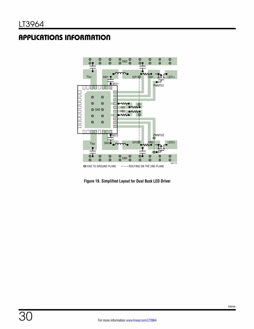
LT3964
30 For more information www.linear.com/LT3964
3964fb
VIAS TO GROUND PLANE ROUTING ON THE 2ND PLANE
BST2
FB1FB2
PWMTG2
VIN2 SW2 ISP2 ISN2 LED2+
GND
BST1 PWMTG1
VIN1 SW1 ISP1 ISN1 LED1+
GND
GND
3964 F19
Figure 19. Simplified Layout for Dual Buck LED Driver
APPLICATIONS INFORMATION
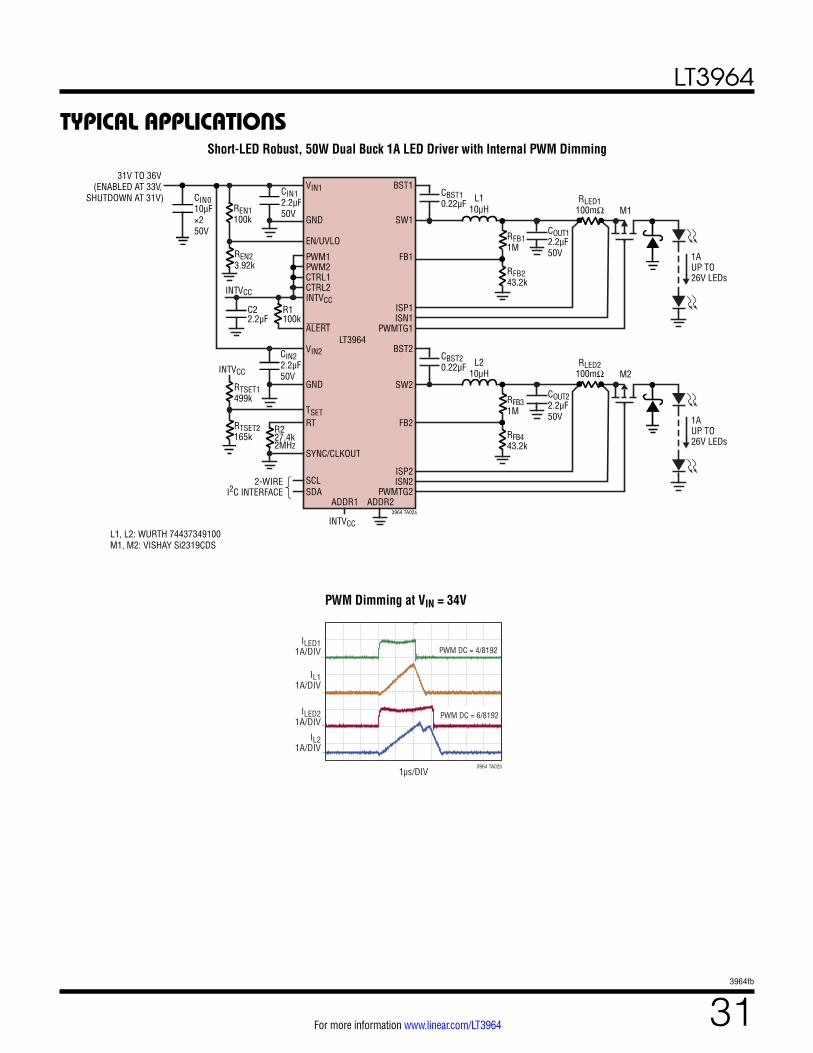
LT3964
31For more information www.linear.com/LT3964
3964fb
TYPICAL APPLICATIONSShort-LED Robust, 50W Dual Buck 1A LED Driver with Internal PWM Dimming
PWM Dimming at VIN = 34V
PWM DC = 4/8192
PWM DC = 6/8192
1µs/DIV
ILED21A/DIV
IL21A/DIV
ILED11A/DIV
IL11A/DIV
3964 TA02b
L110µH
CBST10.22µF
RFB11M
RLED1100mΩ
COUT12.2µF50V 1A
UP TO26V LEDs
M1
RFB243.2k
R1100k
R227.4k2MHz
CIN22.2µF50V
L210µH
CBST20.22µF
RFB31M
RLED2100mΩ
COUT22.2µF50V
CIN12.2µF50VREN1
100k
RTSET1499k
C22.2µF
BST1
LT3964
SW1
VIN1
ISP1ISN1
PWMTG1
CTRL1
BST2
SW2
ISP2ISN2
PWMTG2
1AUP TO26V LEDs
GND
EN/UVLO
CTRL2
PWM1PWM2
INTVCC
ALERT
VIN2
GND
TSETRT
SCLSDA
2-WIREI2C INTERFACE
ADDR1 ADDR2
SYNC/CLKOUT
INTVCC
INTVCC
INTVCC
FB1
FB2
M2
RFB443.2k
REN23.92k
RTSET2165k
31V TO 36V (ENABLED AT 33V,
SHUTDOWN AT 31V) CIN010µF×250V
3964 TA02a
L1, L2: WURTH 74437349100M1, M2: VISHAY Si2319CDS

LT3964
32 For more information www.linear.com/LT3964
3964fb
L210µH
CBST10.22µF
RFB31M
RLED1100mΩ
COUT32.2µF50V 1A
UP TO26V LEDs
M2
RFB443.2k
L3 10µH
CBST20.22µF
RFB51M
RLED2100mΩ
COUT42.2µF50V
CIN22.2µF50VREN3
100k
RTSET1499k
R3100k
C32.2µF
R427.4k2MHz
CIN32.2µF50V
BST1
LT3964
SW1
VIN1
ISP1ISN1
PWMTG1
PWM1
BST2
SW2
ISP2ISN2
PWMTG2
1AUP TO26V LEDs
GND
EN/UVLO
PWM2
CTRL1CTRL2
CTRLCTRL
INTVCC
ALERT
VIN2
GND
TSETRT
SCLSDA
2-WIREI2C INTERFACE
ADDR1 ADDR2
SYNC/CLKOUT
INTVCC
INTVCC
INTVCC
FB1
FB2
M3
RFB643.2k
REN43.92k
RTSET2165k
D1
M1
LT3757
VIN GATE
SENSE
FBX
INTVCC
SHDN/UVLO
SYNC
SSRT
VC GND
VIN6V TO 24V
ILED DERATESAT VIN < 8V
34.5V
REN1105k
REN228k
L1 10µH
CIN110µF
CSS0.1µF
R241.2k300kHz
+RCTRL1100k
RCTRL117.4k
R110k
C110nF
RFB1261k
RFB211.8k
C24.7µF
RSEN10M
COUT147µF50V
COUT4.7µF50V
CTRL
3964 TA03a
L1: VISHAY SILICONIX IHLP-5050FD-01 10μHL2, L3: WURTH 74437349100M1: INFINEON BSC030N04NSM2, M3: VISHAY Si2319CDSD1: DIODES PDS1040
TYPICAL APPLICATIONSMulti-Channel Boost Buck LED Driver
Efficiency
VIN (V)6 8 10 12 14 16 18 20 22 24
80
82
84
86
88
90
92
94
EFFI
CIEN
CY (%
)
Efficiency
3964 TA03b
BOTH CHANNELS ARE ON

LT3964
33For more information www.linear.com/LT3964
3964fb
Matrix LED Driver
TYPICAL APPLICATIONS
L168µH
CBST10.22µF
RFB3274k
31.6kRFB2
RLED2200mΩ
CIN22.2µF
100kREN1
3.92kREN2
499kRTSET1
165kRTSET2
C22.2µF
CIN32.2µF
R3178k
RLED1200mΩ
L268µH
CBST20.22µF
RFB6274k
31.6kRFB5
CIN41µF
CIN61µF
REN349.9k
REN49.02k
CIN51µF R1
100k
CIN71µF
COUT210µF
COUT410µF
RFB11M
RFB41M
COUT1100nF
COUT3100nF
Q1
REN549.9k
REN69.02k
Q2
REN810k
M1
M2
CIN110µF
BST1
LT3964
SW1VIN1
ISP1
ISN1
PWMTG1
CTRL1
BST2
SW2
ISP2
ISN2
PWMTG2
GND
EN/UVLO
CTRL2
PWM1PWM2
INTVCC
ALERT
VIN2
GND
TSET
RT
SCLSDA
2-WIREI2C INTERFACE
ADDR1
ADDR2
SYNC/CLKOUT
360kHz
INTVCC
INTVCC
INTVCC
FB1
FB2
LT3965
DRN8
SRC8DRN7
SRC7DRN6
SRC6DRN5
SRC5DRN4
SRC4DRN3
SRC3DRN2
SRC2DRN1
SRC1
LT3965
DRN8
SRC8DRN7
SRC7DRN6
SRC6DRN5
SRC5DRN4
SRC4DRN3
SRC3DRN2
SRC2DRN1
SRC1
SCLSDA
2-WIREI2C INTERFACE
SCLSDA
2-WIREI2C INTERFACE
ADDR1ADDR2ADDR3ADDR4
31V TO 36V (ENABLED AT 33V, SHUTDOWN AT 31V) VIN
VIN
EN/UVLO
EN/UVLO
ADDR1ADDR2ADDR3ADDR4
31V TO 36V
31V TO 36V
VDD
ALERT
VDD
ALERT
5V
5V
RTCLK
GND
CLOCK (FROM LT3964)
GND
CLOCK
LEDREF LEDREF
LEDREF LEDREFRTCLK CLOCK (FROM LT3964)
ALERT
ALERT
ALERT
INTVCC
LED1+
LED2+
LED1+
LED2+
UP TO 26V LED
UP TO 26V LED
50V×2 50V
50V
50V
50V
50V
50V
REN710k
INTVCC
3964 TA04a
L1, L2: WURTH 7447709680M1, M2: VISHAY Si2319CDS
Single LED PWM Dimming at VIN = 34Vat VIN = 34V
PWM DC = 1/256
5µs/DIV
VCLKOUT5V/DIV
VDRAIN82V/DIV
ILED1500mA/DIV
IL1500mA/DIV
3964 TA04b
Efficiency, VIN = 34V
ILED (mA)50 100 150 200 250 300 350 400 450 500
80
82
84
86
88
90
92
94
96
98
100
EFFI
CIEN
CY (%
)
IN
3964 TA04c
BOTH CHANNELS ARE ON
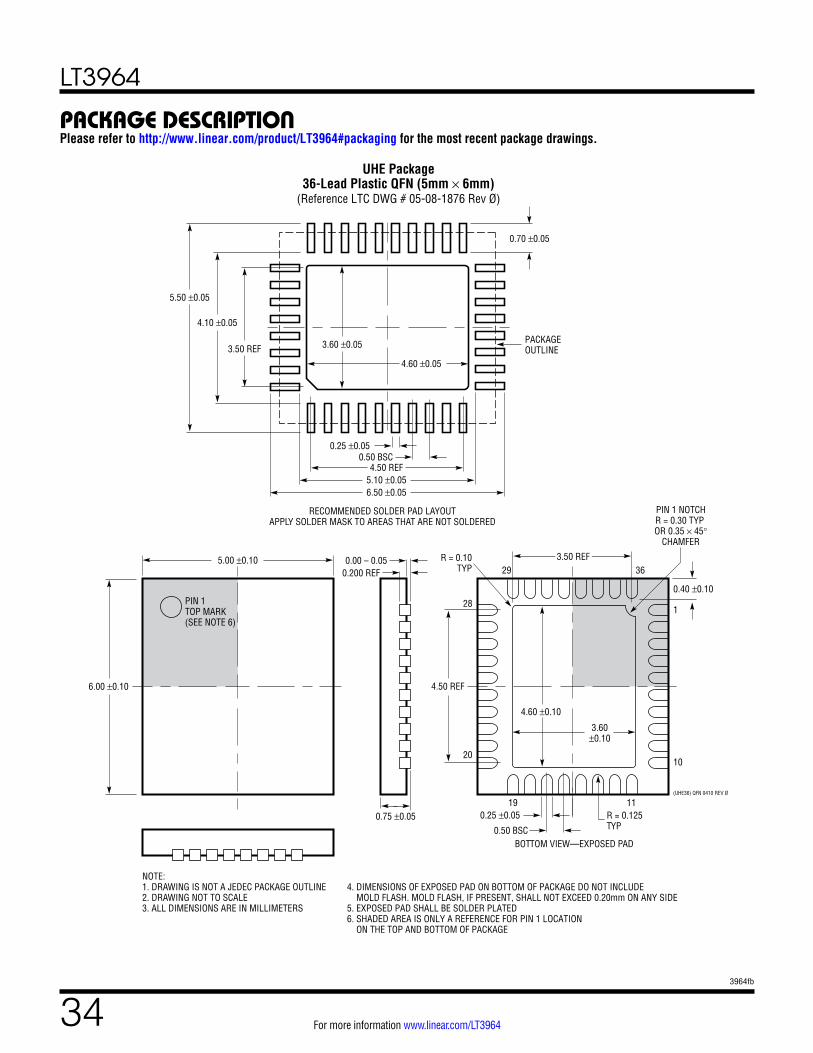
LT3964
34 For more information www.linear.com/LT3964
3964fb
PACKAGE DESCRIPTION
5.00 ±0.10
NOTE:1. DRAWING IS NOT A JEDEC PACKAGE OUTLINE2. DRAWING NOT TO SCALE3. ALL DIMENSIONS ARE IN MILLIMETERS
PIN 1TOP MARK(SEE NOTE 6)
1
1020
28
1119
3629
BOTTOM VIEW—EXPOSED PAD
4.50 REF6.00 ±0.10
R = 0.125TYP
0.25 ±0.05
4.60 ±0.10
3.60±0.10
(UHE36) QFN 0410 REV Ø
0.50 BSC
4.60 ±0.05
3.60 ±0.05
0.75 ±0.05
0.00 – 0.050.200 REF
RECOMMENDED SOLDER PAD LAYOUTAPPLY SOLDER MASK TO AREAS THAT ARE NOT SOLDERED
3.50 REF
0.40 ±0.10
0.70 ±0.05
0.50 BSC4.50 REF
3.50 REF
4.10 ±0.05
5.50 ±0.05
5.10 ±0.056.50 ±0.05
0.25 ±0.05
PACKAGEOUTLINE
4. DIMENSIONS OF EXPOSED PAD ON BOTTOM OF PACKAGE DO NOT INCLUDE MOLD FLASH. MOLD FLASH, IF PRESENT, SHALL NOT EXCEED 0.20mm ON ANY SIDE5. EXPOSED PAD SHALL BE SOLDER PLATED6. SHADED AREA IS ONLY A REFERENCE FOR PIN 1 LOCATION ON THE TOP AND BOTTOM OF PACKAGE
PIN 1 NOTCHR = 0.30 TYP OR 0.35 × 45°
CHAMFER
R = 0.10TYP
UHE Package36-Lead Plastic QFN (5mm × 6mm)
(Reference LTC DWG # 05-08-1876 Rev Ø)
Please refer to http://www.linear.com/product/LT3964#packaging for the most recent package drawings.

LT3964
35For more information www.linear.com/LT3964
3964fb
REVISION HISTORYREV DATE DESCRIPTION PAGE NUMBER
A 12/17 Block Diagram: corrected MOSFET symbol orientation for top switch, bottom switch and M1 MOSFETs. 12
B 3/18 Note 2: RT pin added. 5
Information furnished by Analog Devices is believed to be accurate and reliable. However, no responsibility is assumed by Analog Devices for its use, nor for any infringements of patents or other rights of third parties that may result from its use. Specifications subject to change without notice. No license is granted by implication or otherwise under any patent or patent rights of Analog Devices.

LT3964
36 For more information www.linear.com/LT3964
3964fb
LT 0318 REV B • PRINTED IN USAwww.linear.com/LT3964
© ANALOG DEVICES, INC. 2017
RELATED PARTS
TYPICAL APPLICATIONDual 1A Single LED Driver Efficiency, ILED = 1A
VIN (V)6 8 10 12 14 16 18 20 22 24
70
72
74
76
78
80
82
84
86
88
90
EFFI
CIEN
CY (%
)
LED
3964 TA05b
BOTH CHANNELS ARE ON
L12.2µH
CBST10.22µF
RFB11M
RLED1100mΩ
COUT12.2µF
M1
RFB1357k
R1100k
R227.4k2MHz
CIN22.2µF
CBST20.22µF
RFB31M
RLED2100mΩ
COUT22.2µF
CIN12.2µFREN1
100k
RTSET1499k
C22.2µF
BST1
LT3964
SW1
VIN1
ISP1ISN1
PWMTG1
CTRL1
BST2
SW2
ISP2ISN2
PWMTG2
GND
EN/UVLO
CTRL2
PWM1PWM2
INTVCC
ALERT
VIN2
GND
TSETRT
SCLSDA
ADDR1 ADDR2
SYNC/CLKOUT
INTVCC
INTVCC
FB1
FB2
M2
RFB4357k
REN228.7k
RTSET2165k
L22.2µH
INTVCC
2-WIREI2C INTERFACE
CIN310µF
6V TO 24V (ENABLED AT 6V, SHUTDOWN AT 5.2V)
3964 TA05a
L1, L2: COILCRAFT XAL4020-222MEBM1, M2: VISHAY Si2365EDS
PART NUMBER DESCRIPTION COMMENTS
LT3922 36V, 2A Synchronous Step-Up LED Driver VIN(MIN) = 2.8V, VIN(MAX) = 36V, VOUT = 40V, 128:1 Internal Dimming and 5,000:1 External Dimming, ISD = 1μA, 4mm × 5mm QFN-28
LT3932 36V, 2A Synchronous Step-Down LED Driver VIN(MIN) = 3.6V, VIN(MAX) = 36V, VOUT = 0V to 36V, 128:1 Internal Dimming and 5,000:1 External Dimming, ISD = 1μA, 4mm × 5mm QFN-28
LT3952 60V, 4A Synchronous Step-Up LED Driver VIN(MIN) = 3V, VIN(MAX) = 42V, VOUT = 0V to 60V, 5:1 Internal Dimming and 4,000:1 External Dimming, ISD = 1μA, TSSOP-28E
LT3795 High Side 110V, 1MHz LED Driver with 3,000:1 PWM Dimming with Spread Spectrum Frequency Modulation
VIN(MIN) = 4.5V, VIN(MAX) = 110V, VOUT = 110VMAX, 3000:1 PWM, 20:1 Analog, ISD = <1µA, TSSOP-28E
LT3956 80VIN/80VOUT, ISW = 3.3A, 1MHz LED Driver with 3,000:1 PWM Dimming
VIN(MIN) = 4.5V, VIN(MAX) = 80V, VOUT = 40VMAX, 3000:1 PWM, 20:1 Analog, ISD = <1µA, 5mm × 6mm QFN-36
LT3761 High Side 100V, 1MHz LED Controller with 3,000:1 PWM Dimming and Internal PWM Generator
VIN(MIN) = 4.5V, VIN(MAX) = 60V, VOUT = 80VMAX, 3000:1 PWM, 20:1 Analog, ISD = <1µA, MSOP-16E
LT3755/LT3755-1/LT3755-2
High Side 75V, 1MHz LED Controller with 3,000:1 PWM Dimming
VIN(MIN) = 4.5V, VIN(MAX) = 40V, VOUT = 5V to 75V, 3000:1 PWM, 20:1 Analog, ISD = <1µA, 3mm × 3mm QFN-16 and MSOP-16E
LT3756/LT3756-1/LT3756-2
High Side 100V, 1MHz LED Controller with 3,000:1 PWM Dimming
VIN(MIN) = 6.0V, VIN(MAX) = 100V, VOUT = 5V to 100V, 3000:1 PWM, 20:1 Analog, ISD = <1µA, 3mm × 3mm QFN-16 and MSOP-16E
Related Documents