LTC3129 1 3129fc For more information www.linear.com/LTC3129 TYPICAL APPLICATION FEATURES DESCRIPTION 15V, 200mA Synchronous Buck-Boost DC/DC Converter with 1.3µA Quiescent Current The LTC ® 3129 is a high efficiency, 200mA buck-boost DC/DC converter with a wide V IN and V OUT range. It includes an accurate RUN pin threshold to allow predictable regula- tor turn-on and a maximum power point control (MPPC) capability that ensures maximum power extraction from non-ideal power sources such as photovoltaic panels. The LTC3129 employs an ultralow noise, 1.2MHz PWM switching architecture that minimizes solution footprint by allowing the use of tiny, low profile inductors and ceramic capacitors. Built-in loop compensation and soft-start simplify the design. For high efficiency operation at light loads, automatic Burst Mode operation can be selected, reducing the quiescent current to just 1.3µA. Additional features include a power good output, less than 10nA of shutdown current and thermal shutdown. The LTC3129 is available in thermally enhanced 3mm × 3mm QFN and 16-lead MSOP packages. For fixed output voltage options, see the functionally equivalent LTC3129-1, which eliminates the need for an external feedback divider. L, LT, LTC, LTM, Linear Technology, the Linear logo and Burst Mode are registered trademarks and PowerPath is a trademark of Linear Technology Corporation. All other trademarks are the property of their respective owners. APPLICATIONS n Regulates V OUT Above, Below or Equal to V IN n Wide V IN Range: 2.42V to 15V, 1.92V to 15V After Start-Up (Bootstrapped) n Wide V OUT Range: 1.4V to 15.75V n 200mA Output Current in Buck Mode n Single Inductor n 1.3µA Quiescent Current n Programmable Maximum Power Point Control n 1.2MHz Ultralow Noise PWM n Current Mode Control n Pin Selectable Burst Mode ® Operation n Up to 95% Efficiency n Accurate RUN Pin Threshold n Power Good Indicator n 10nA Shutdown Current n Thermally Enhanced 3mm × 3mm QFN and 16-Lead MSOP Packages n Industrial Wireless Sensor Nodes n Post-Regulator for Harvested Energy n Solar Panel Post-Regulator/Charger n Intrinsically Safe Power Supplies n Wireless Microphones n Avionics-Grade Wireless Headsets BST1 V OUT V OUT SW1 SW2 LTC3129 22nF BST2 PGOOD GND FB V CC V IN 2.42V TO 15V V IN V CC RUN MPPC PWM 22nF 10μH 10μF 10μF 10pF 2.2μF 3129 TA01a PGND 3.32M 1.02M 5V AT 200mA, V IN > 5V 5V AT 100mA, V IN < 5V Efficiency and Power Loss vs Load 100 OUTPUT CURRENT (mA) 0.01 EFFICIENCY (%) POWER LOSS (mW) 70 80 90 50 30 20 60 40 10 0 1000 100 0.1 10 1 0.01 3129 TA01b 0.1 100 1000 10 1 V IN = 2.5V V IN = 3.6V V IN = 5V V IN = 15V EFFICIENCY POWER LOSS V OUT = 5V

Welcome message from author
This document is posted to help you gain knowledge. Please leave a comment to let me know what you think about it! Share it to your friends and learn new things together.
Transcript

LTC3129
13129fc
For more information www.linear.com/LTC3129
Typical applicaTion
FeaTures DescripTion
15V, 200mA Synchronous Buck-Boost DC/DC Converter with 1.3µA Quiescent Current
The LTC®3129 is a high efficiency, 200mA buck-boost DC/DC converter with a wide VIN and VOUT range. It includes an accurate RUN pin threshold to allow predictable regula-tor turn-on and a maximum power point control (MPPC) capability that ensures maximum power extraction from non-ideal power sources such as photovoltaic panels.
The LTC3129 employs an ultralow noise, 1.2MHz PWM switching architecture that minimizes solution footprint by allowing the use of tiny, low profile inductors and ceramic capacitors. Built-in loop compensation and soft-start simplify the design. For high efficiency operation at light loads, automatic Burst Mode operation can be selected, reducing the quiescent current to just 1.3µA.
Additional features include a power good output, less than 10nA of shutdown current and thermal shutdown.
The LTC3129 is available in thermally enhanced 3mm × 3mm QFN and 16-lead MSOP packages. For fixed output voltage options, see the functionally equivalent LTC3129-1, which eliminates the need for an external feedback divider.L, LT, LTC, LTM, Linear Technology, the Linear logo and Burst Mode are registered trademarks and PowerPath is a trademark of Linear Technology Corporation. All other trademarks are the property of their respective owners.
applicaTions
n Regulates VOUT Above, Below or Equal to VINn Wide VIN Range: 2.42V to 15V, 1.92V to 15V After
Start-Up (Bootstrapped)n Wide VOUT Range: 1.4V to 15.75Vn 200mA Output Current in Buck Moden Single Inductorn 1.3µA Quiescent Currentn Programmable Maximum Power Point Controln 1.2MHz Ultralow Noise PWMn Current Mode Controln Pin Selectable Burst Mode® Operationn Up to 95% Efficiencyn Accurate RUN Pin Thresholdn Power Good Indicatorn 10nA Shutdown Currentn Thermally Enhanced 3mm × 3mm QFN and
16-Lead MSOP Packages
n Industrial Wireless Sensor Nodesn Post-Regulator for Harvested Energyn Solar Panel Post-Regulator/Chargern Intrinsically Safe Power Suppliesn Wireless Microphonesn Avionics-Grade Wireless Headsets
BST1VOUT VOUT
SW1 SW2
LTC3129
22nF
BST2
PGOOD
GND
FB
VCC
VIN
2.42V TO 15VVIN
VCC
RUN
MPPC
PWM
22nF 10µH
10µF
10µF 10pF
2.2µF
3129 TA01a
PGND
3.32M
1.02M
5V AT 200mA, VIN > 5V5V AT 100mA, VIN < 5V
Efficiency and Power Loss vs Load100
OUTPUT CURRENT (mA)0.01
EFFI
CIEN
CY (%
)
POWER LOSS (m
W)
70
80
90
50
30
20
60
40
10
0
1000
100
0.1
10
1
0.01
3129 TA01b
0.1 100 1000101
VIN = 2.5VVIN = 3.6VVIN = 5VVIN = 15V
EFFICIENCY
POWER LOSS
VOUT = 5V

LTC3129
23129fc
For more information www.linear.com/LTC3129
absoluTe MaxiMuM raTings
VIN, VOUT Voltages .................................... –0.3V to 18VSW1 DC Voltage ............................ –0.3V to (VIN + 0.3V) SW2 DC Voltage..........................–0.3V to (VOUT + 0.3V)SW1, SW2 Pulsed (<100ns) Voltage ..............–1V to 19VBST1 Voltage .................... (SW1 – 0.3V) to (SW1 + 6V)BST2 Voltage .................... (SW2 – 0.3V) to (SW2 + 6V)RUN, PGOOD Voltages ............................... –0.3V to 18V
VCC, FB, PWM, MPPC Voltages .................... –0.3V to 6VPGOOD Sink Current .............................................15mAOperating Junction Temperature Range (Notes 2, 5) ............................................ –40°C to 125°CStorage Temperature Range .................. –65°C to 150°CMSE Lead Temperature (Soldering, 10 sec) .......... 300°C
(Notes 1, 8)
16 15 14 13
5 6 7 8
TOP VIEW
UD PACKAGE16-LEAD (3mm × 3mm) PLASTIC QFN
9
10
11
12
4
3
2
1BST1
VIN
VCC
RUN
VOUT
PGOOD
PWM
NC
SW1
PGND
SW2
BST2
MPP
C
GND FB NC
17PGND
TJMAX = 125°C, θJC = 7.5°C/W, θJA = 68°C/W (NOTE 6)
EXPOSED PAD (PIN 17) IS PGND, MUST BE SOLDERED TO PCB
12345678
VCCRUN
MPPCGND
FBNCNC
PWM
161514131211109
VINBST1SW1PGNDSW2BST2VOUTPGOOD
TOP VIEW
MSE PACKAGE16-LEAD PLASTIC MSOP
17PGND
TJMAX = 125°C, θJC = 10°C/W, θJA = 40°C/W (NOTE 6)
EXPOSED PAD (PIN 17) IS PGND, MUST BE SOLDERED TO PCB
pin conFiguraTion
orDer inForMaTionLEAD FREE FINISH TAPE AND REEL PART MARKING* PACKAGE DESCRIPTION TEMPERATURE RANGE
LTC3129EUD#PBF LTC3129EUD#TRPBF LGDR 16-Lead (3mm × 3mm) Plastic QFN –40°C to 125°C
LTC3129IUD#PBF LTC3129IUD#TRPBF LGDR 16-Lead (3mm × 3mm) Plastic QFN –40°C to 125°C
LTC3129EMSE#PBF LTC3129EMSE#TRPBF 3129 16-Lead Plastic MSOP –40°C to 125°C
LTC3129IMSE#PBF LTC3129IMSE#TRPBF 3129 16-Lead Plastic MSOP –40°C to 125°C
Consult LTC Marketing for parts specified with wider operating temperature ranges.For more information on lead free part marking, go to: http://www.linear.com/leadfree/ For more information on tape and reel specifications, go to: http://www.linear.com/tapeandreel/. Some packages are available in 500 unit reels through designated sales channels with #TRMPBF suffix.

LTC3129
33129fc
For more information www.linear.com/LTC3129
elecTrical characTerisTics The l denotes the specifications which apply over the specified operating junction temperature range, otherwise specifications are at TA = 25°C (Note 2). Unless otherwise noted, VIN = 12V, VOUT = 5V.
PARAMETER CONDITIONS MIN TYP MAX UNITSVIN Start-Up Voltage l 2.25 2.42 VInput Voltage Range VCC > 2.42V (Back-Driven) l 1.92 15 VVIN UVLO Threshold (Rising) VCC > 2.42V (Back-Driven) l 1.8 1.9 2.0 VVIN UVLO Hysteresis l 80 100 130 mVOutput Voltage Adjust Range l 1.4 15.75 VFeedback Voltage l 1.151 1.175 1.199 VFeedback Input Current FB = 1.25V 0.1 10 nAQuiescent Current (VIN) – Shutdown RUN = 0V, Including Switch Leakage 10 100 nAQuiescent Current (VIN) UVLO Either VIN or VCC Below Their UVLO Threshold, or
RUN Below the Threshold to Enable Switching1.9 3 µA
Quiescent Current – Burst Mode Operation Measured on VIN, FB > 1.25V PWM = 0V, RUN = VIN
1.3 2.0 µA
N-Channel Switch Leakage on VIN and VOUT SW1 = 0V, VIN = 15V SW2 = 0V, VOUT = 15V RUN = 0V
10 50 nA
N-Channel Switch On-Resistance VCC = 4V 0.75 ΩInductor Average Current Limit VOUT > UV Threshold (Note 4)
VOUT < UV Threshold (Note 4)l
l
220 80
275 130
350 200
mA mA
Inductor Peak Current Limit (Note 4) l 400 500 680 mAMaximum Boost Duty Cycle FB = 1.10V. Percentage of Period SW2 is Low in
Boost Mode (Note 7)l 85 89 95 %
Minimum Duty Cycle FB = 1.25V. Percentage of Period SW1 is High in Buck Mode (Note 7)
l 0 %
Switching Frequency PWM = VCC l 1.0 1.2 1.4 MHzSW1 and SW2 Minimum Low Time (Note 3) 90 nsMPPC Voltage l 1.12 1.175 1.22 VMPPC Input Current MPPC = 5V 1 10 nARUN Threshold to Enable VCC l 0.5 0.9 1.15 VRUN Threshold to Enable Switching (Rising) VCC > 2.4V l 1.16 1.22 1.28 VRUN (Switching) Threshold Hysteresis 50 80 120 mVRUN Input Current RUN = 15V 1 10 nAPWM Input High l 1.6 VPWM Input Low l 0.5 VPWM Input Current PWM = 5V 0.1 1 µASoft-Start Time 3 msVCC Voltage VIN > 4.85V l 3.4 4.1 4.7 VVCC Dropout Voltage (VIN – VCC) VIN = 3.0V, Switching
VIN = 2.0V (VCC in UVLO)35 0
60 2
mV mV
VCC UVLO Threshold (Rising) l 2.1 2.25 2.42 VVCC UVLO Hysteresis 60 mVVCC Current Limit VCC = 0V l 4 20 60 mAVCC Back-Drive Voltage (Maximum) l 5.5 VVCC Input Current (Back-Driven) VCC = 5.5V (Switching) 2 4 mAVCC Leakage to VIN if VCC > VIN VCC = 5.5V, VIN = 1.8V, Measured on VIN –27 µAVOUT UV Threshold (Rising) l 0.95 1.15 1.35 V

LTC3129
43129fc
For more information www.linear.com/LTC3129
elecTrical characTerisTics
Note 1: Stresses beyond those listed under Absolute Maximum Ratings may cause permanent damage to the device. Exposure to any Absolute Maximum Rating condition for extended periods may affect device reliability and lifetime.Note 2: The LTC3129 is tested under pulsed load conditions such that TJ ≈ TA. The LTC3129E is guaranteed to meet specifications from 0°C to 85°C junction temperature. Specifications over the –40°C to 125°C operating junction temperature range are assured by design, characterization and correlation with statistical process controls. The LTC3129I is guaranteed over the full –40°C to 125°C operating junction temperature range. The junction temperature (TJ) is calculated from the ambient temperature (TA) and power dissipation (PD) according to the formula: TJ = TA + (PD • θJA°C/W), where θJA is the package thermal impedance. Note that the maximum ambient temperature consistent with these specifications, is determined by specific operating conditions in conjunction with board layout, the rated thermal package thermal resistance and other environmental factors.Note 3: Specification is guaranteed by design and not 100% tested in production.
PARAMETER CONDITIONS MIN TYP MAX UNITSVOUT UV Hysteresis 150 mVVOUT Current – Shutdown RUN = 0V, VOUT = 15V Including Switch Leakage 10 100 nAVOUT Current – Sleep PWM = 0V, FB = 1.25V 10 nAVOUT Current – Active PWM = VCC, VOUT = 15V (Note 4), FB = 1.25V 5 9 µAPGOOD Threshold, Falling Referenced to Programmed VOUT Voltage –5.5 –7.5 –10 %PGOOD Hysteresis Referenced to Programmed VOUT Voltage 2.5 %PGOOD Voltage Low ISINK = 1mA 250 300 mVPGOOD Leakage PGOOD = 15V 1 50 nA
The l denotes the specifications which apply over the specified operating junction temperature range, otherwise specifications are at TA = 25°C (Note 2). Unless otherwise noted, VIN = 12V, VOUT = 5V.
Note 4: Current measurements are made when the output is not switching.Note 5: This IC includes overtemperature protection that is intended to protect the device during momentary overload conditions. Junction temperature will exceed 125°C when overtemperature protection is active. Continuous operation above the specified maximum operating junction temperature may result in device degradation or failure.Note 6: Failure to solder the exposed backside of the package to the PC board ground plane will result in a much higher thermal resistance.Note 7: Switch timing measurements are made in an open-loop test configuration. Timing in the application may vary somewhat from these values due to differences in the switch pin voltage during non-overlap durations when switch pin voltage is influenced by the magnitude and duration of the inductor current.Note 8: Voltage transients on the switch pin(s) beyond the DC limits specified in the Absolute Maximum Ratings are non-disruptive to normal operation when using good layout practices as described elsewhere in the data sheet and application notes and as seen on the product demo board.
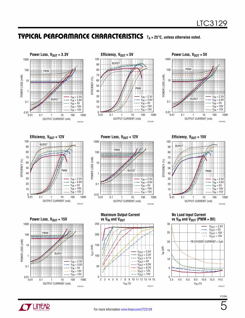
Efficiency, VOUT = 2.5V Efficiency, VOUT = 3.3V
Typical perForMance characTerisTics TA = 25°C, unless otherwise noted.
Power Loss, VOUT = 2.5V
OUTPUT CURRENT (mA)0.01
EFFI
CIEN
CY (%
)
100
90
70
50
40
80
60
30
20
10
0100.1
3129 G01
10001 100
VIN = 2.5VVIN = 3.6VVIN = 5VVIN = 10VVIN = 15V
BURST
PWM
OUTPUT CURRENT (mA)0.01
EFFI
CIEN
CY (%
)
100
90
70
50
40
80
60
30
20
10
0100.1
3129 G03
10001 100
VIN = 2.5VVIN = 3.6VVIN = 5VVIN = 10VVIN = 15V
PWM
BURST
OUTPUT CURRENT (mA)0.01
POW
ER L
OSS
(mW
)
1000
100
10
1
0.1
0.01100.1
3129 G02
10001 100
VIN = 2.5VVIN = 3.6VVIN = 5VVIN = 10VVIN = 15V
BURST
PWM
LTC3129
53129fc
For more information www.linear.com/LTC3129
Typical perForMance characTerisTics
Efficiency, VOUT = 12V
Maximum Output Current vs VIN and VOUT
Efficiency, VOUT = 5V
TA = 25°C, unless otherwise noted.
Power Loss, VOUT = 3.3V Power Loss, VOUT = 5V
Power Loss, VOUT = 12V Efficiency, VOUT = 15V
Power Loss, VOUT = 15V
VIN (V)2
I OUT
(mA)
250
200
150
100
50
0133 4
3129 G11
1510 1411 1285 96 7
VOUT = 2.5VVOUT = 3.3VVOUT = 4.1VVOUT = 5VVOUT = 6.9VVOUT = 8.2VVOUT = 12VVOUT = 15V
No Load Input Current vs VIN and VOUT (PWM = 0V)
OUTPUT CURRENT (mA)0.01
EFFI
CIEN
CY (%
)
100
90
70
50
40
80
60
30
20
10
0100.1
3129 G05
10001 100
BURST
PWM
VIN = 2.5VVIN = 3.6VVIN = 5VVIN = 10VVIN = 15V
OUTPUT CURRENT (mA)0.01
EFFI
CIEN
CY (%
)
100
90
70
50
40
80
60
30
20
10
0100.1
3129 G09
10001 100
PWM
BURST
VIN = 2.5VVIN = 3.6VVIN = 5VVIN = 10VVIN = 15V
OUTPUT CURRENT (mA)0.01
POW
ER L
OSS
(mW
)
1000
100
10
1
0.1
0.01100.1
3129 G04
10001 100
BURST
PWM
VIN = 2.5VVIN = 3.6VVIN = 5VVIN = 10VVIN = 15V
OUTPUT CURRENT (mA)0.01
POW
ER L
OSS
(mW
)
1000
100
10
1
0.1
0.01100.1
3129 G06
10001 100
PWM
BURSTVIN = 2.5VVIN = 3.6VVIN = 5VVIN = 10VVIN = 15V
OUTPUT CURRENT (mA)0.01
EFFI
CIEN
CY (%
)
100
90
70
50
40
40
80
60
30
20
10
0100.1
3129 G07
10001 100
BURST
PWM
VIN = 2.5VVIN = 3.6VVIN = 5VVIN = 10VVIN = 15V
OUTPUT CURRENT (mA)0.01
POW
ER L
OSS
(mW
)
1000
100
10
1
0.1
0.01100.1
3129 G08
10001 100
PWM
BURST
VIN = 2.5VVIN = 3.6VVIN = 5VVIN = 10VVIN = 15V
OUTPUT CURRENT (mA)0.01
POW
ER L
OSS
(mW
)
1000
100
10
1
0.1
0.01100.1
3129 G10
10001 100
BURST
VIN = 2.5VVIN = 3.6VVIN = 5VVIN = 10VVIN = 15V
PWM
VIN (V)2.5
I IN (µ
A)
30
25
20
15
10
5
012.5
3129 G12
14.510.54.5 8.56.5
VOUT = 2.5VVOUT = 5VVOUT = 10VVOUT = 15V
FB DIVIDER CURRENT = 2µA

LTC3129
63129fc
For more information www.linear.com/LTC3129
Typical perForMance characTerisTics
Accurate RUN Threshold vs Temperature (Normalized to 25°C)
Maximum Output Current vs Temperature (Normalized to 25°C)
VCC Dropout Voltage vs Temperature (PWM Mode, Switching)
VCC Dropout Voltage vs VIN (PWM Mode, Switching)
Fixed Frequency PWM Waveforms
TA = 25°C, unless otherwise noted.
Average Input Current Limit vs MPPC Voltage
Burst Mode Threshold vs VIN and VOUT Switch RDS(ON) vs Temperature
TEMPERATURE (°C)–45
R DS(
ON) (
Ω)
1.3
1.2
1.1
1.0
0.8
0.7
0.6
0.5
0.9
0.4–20
3129 G14
13055 10580305
VCC = 2.5VVCC = 3VVCC = 4VVCC = 5V
FB Voltage vs Temperature (Normalized to 25°C)
VIN (V)2
LOAD
(mA)
80
70
60
40
30
20
10
50
04
3129 G13
1610 141286
VOUT = 2.5VVOUT = 3.3VVOUT = 4.1VVOUT = 5VVOUT = 6.9VVOUT = 8.2VVOUT = 12VVOUT = 15V
TEMPERATURE (°C)–45
CHAN
GE IN
FB
VOLT
AGE
(%)
1.00
0.50
0.75
0
–0.50
–0.75
–0.25
0.25
–1.00–20
3129 G15
13055 10580305
TEMPERATURE (°C)–45
CHAN
GE IN
RUN
THR
ESHO
LD (%
)
2
0
–1
1
–2–20
3129 G16
13055 10580305MPPC PIN VOLTAGE (V)
1.13
PERC
ENTA
GE O
F FU
LL IN
PUT
CURR
ENT
(%) 100
90
70
60
50
40
30
20
10
80
01.135
3129 G17
1.171.1651.161.1551.145 1.151.14TEMPERATURE (°C)
–45
CHAN
GE IN
MAX
IMUM
OUT
PUT
CURR
ENT
(%) 15
10
0
–5
5
–15
–10
–20
3129 G18
13055 10580305
TEMPERATURE (°C)–45
DROP
OUT
(mV)
60
50
30
20
40
0
10
–20
3129 G19
13055 10580305VIN (V)
2
DROP
OUT
(mV)
60
50
30
20
40
0
10
2.25
3129 G20
43 3.5 3.753.252.752.5
L = 10µHVIN = 7VVOUT = 5VIOUT = 200mA
SW25V/DIV
SW15V/DIV
3129 G21500ns/DIV
IL200mA/DIV

LTC3129
73129fc
For more information www.linear.com/LTC3129
Fixed Frequency Ripple on VOUT
Typical perForMance characTerisTics
Step Load Transient Response in Fixed Frequency
Step Load Transient Response in Burst Mode Operation
PGOOD Response to a Drop On VOUT
Burst Mode Waveforms Burst Mode Ripple on VOUT
Start-Up Waveforms
TA = 25°C, unless otherwise noted.
MPPC Response to a Step Load
L = 10µHVIN = 7VVOUT = 5VIOUT = 200mACOUT = 10µF
3129 G22200ns/DIV
IL200mA/DIV
VOUT20mV/DIV
L = 10µHVIN = 7VVOUT = 5VIOUT = 5mACOUT = 22µF (WITH THE RECOMMENDEDFEEDFORWARD CAPACITOR)
3129 G24100µs/DIV
IL100mA/DIV
VOUT100mV/DIV
VIN = 7VVOUT = 5VIOUT = 50mACOUT = 22µF
3129 G251ms/DIV
IVIN200mA/DIV
VOUT5V/DIV
VCC5V/DIV
RUN5V/DIV
L = 10µHVIN = 7VVOUT = 5VCOUT = 10µFIOUT = 50mA to 150mA STEP
3129 G26500µs/DIV
IVOUT100mA/DIV
VOUT100mV/DIV
L = 10µHVIN = 7VVOUT = 5VCOUT = 22µF (WITH THE RECOMMENDEDFEEDFORWARD CAPACITOR)IOUT = 5mA to 125mA STEP
3129 G27500µs/DIV
IVOUT100mA/DIV
VOUT100mV/DIV
VOUT = 5V3129 G281ms/DIV
PGOOD2V/DIV
VOUT2V/DIV
VIN = 5VOCVMPPC SET TO 3.5VCIN = 22µF, RIN = 10Ω,VOUT = 5V, COUT = 22µFIOUT = 25mA to 125mA STEP
3129 G292ms/DIV
IVOUT100mA/DIV
VOUT2V/DIV
VIN2V/DIV
L = 10µHVIN = 7VVOUT = 5VIOUT = 5mACOUT = 22µF
3129 G2350µs/DIV
IL200mA/DIV
SW25V/DIV
SW15V/DIV

LTC3129
83129fc
For more information www.linear.com/LTC3129
pin FuncTionsBST1 (Pin 1/Pin 15): Bootstrapped Floating Supply for High Side NMOS Gate Drive. Connect to SW1 through a 22nF capacitor, as close to the part as possible. The value is not critical. Any value from 4.7nF to 47nF may be used.
VIN (Pin 2/Pin 16): Input Voltage for the Converter. Connect a minimum of 4.7µF ceramic decoupling capacitor from this pin to the ground plane, as close to the pin as possible.
VCC (Pin 3/Pin 1): Output voltage of the internal voltage regulator. This is the supply pin for the internal circuitry. Bypass this output with a minimum of 2.2µF ceramic capacitor close to the pin. This pin may be back-driven by an external supply, up to a maximum of 5.5V.
RUN (Pin 4/Pin 2): Input to the Run Comparator. Pull this pin above 1.1V to enable the VCC regulator and above 1.28V to enable the converter. Connecting this pin to a resistor divider from VIN to ground allows programming a VIN start threshold higher than the 1.8V (typical) VIN UVLO threshold. In this case, the typical VIN turn-on threshold is determined by VIN = 1.22V • [1+(R3/R4)] (see Figure 2).
MPPC (Pin 5/Pin 3): Maximum Power Point Control Pro-gramming Pin. Connect this pin to a resistor divider from VIN to ground to enable the MPPC functionality. If the VOUT load is greater than what the power source can provide, the MPPC will reduce the inductor current to regulate VIN to a voltage determined by: VIN = 1.175V • [1+(R5/R6)] (see Figure 3). By setting the VIN regulation voltage appro-priately, maximum power transfer from the limited source is assured. Note this pin is very noise sensitive, therefore minimize trace length and stray capacitance. Please refer to the Applications Information section for more detail on programming the MPPC for different sources. If this function is not needed, tie the pin to VCC.
GND (Pin 6/Pin 4): Signal Ground. Provide a short direct PCB path between GND and the ground plane where the exposed pad is soldered.
FB (Pin 7/Pin 5): Feedback Input to the Error Amplifier. Connect to a resistor divider from VOUT to ground. The output voltage can be adjusted from 1.4V to 15.75V by:
VOUT = 1.175V • [1+(R1/R2)]. Note this pin is very noise sensitive, therefore minimize trace length and stray ca-pacitance.
NC (Pins 8, 9/Pins 6, 7): Unused. These pins should be grounded.
PWM (Pin 10/Pin 8): Mode Select Pin.
PWM = Low (ground): Enables automatic Burst Mode operation.
PWM = High (tie to VCC): Fixed frequency PMW opera-tion.
This pin should not be allowed to float. It has an internal 5M pull-down resistor.
PGOOD (Pin 11/Pin 9): Open drain output that pulls to ground when FB drops too far below its regulated voltage. Connect a pull-up resistor from this pin to a positive sup-ply. This pin can sink up to the absolute maximum rating of 15mA when low. Refer to the Operation section of the data sheet for more detail.
VOUT (Pin 12/Pin 10): Output voltage of the converter. Connect a minimum value of 4.7µF ceramic capacitor from this pin to the ground plane, as close to the pin as possible.
BST2 (Pin 13/Pin 11): Bootstrapped floating supply for high side NMOS gate drive. Connect to SW2 through a 22nF capacitor, as close to the part as possible. The value is not critical. Any value from 4.7nF to 47nF may be used.
SW2 (Pin 14/Pin 12): Switch Pin. Connect to one side of the inductor. Keep PCB trace lengths as short and wide as possible to reduce EMI.
PGND (Pin 15, Exposed Pad Pin 17/Pin 13, Exposed Pad Pin 17): Power Ground. Provide a short direct PCB path between PGND and the ground plane. The exposed pad must also be soldered to the PCB ground plane. It serves as a power ground connection, and as a means of conducting heat away from the die.
SW1 (Pin 16/Pin 14): Switch Pin. Connect to one side of the inductor. Keep PCB trace lengths as short and wide as possible to reduce EMI.
(QFN/MSOP)
LTC3129
93129fc
For more information www.linear.com/LTC3129
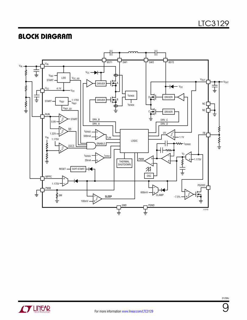
block DiagraM
3129 BD
LDOVREF
START
VREF
VCC
VCC
VCC_GD
START
START
4.1V
1.175VVREF
+–
SD
UVLO
+–
–+
+–
–+ THERMAL
SHUTDOWN
+–
–+PWM
600mV
–7.5%
OSC
GND
SLEEP
100mV
RESET
ENABLE
ILIM
IZEROISENSE
20mA
ISENSE
VREF_GD
500mA
PGND
CLAMP
+–
1.175V
–+
–+
–+
–+
DRIVER
DRIVER
DRIVER
DRIVER
ISENSE
ISENSE
DRV_C
1.1V
UV
NC
VOUT
VCC
VOUT
NC
FB
DRV_D
DRV_B
DRV_A
ISENSE
LOGIC
PGOOD
SOFT-START
+–
MPPC
RUN
VCC
VINVIN
BST1 SW1 SW2
D
C
A
B
BST2
PWM
SLEEP
VIN
0.9V
1.22V
1.175V
1.175V
VC
5M
LTC3129
103129fc
For more information www.linear.com/LTC3129
operaTionINTRODUCTION
The LTC3129 is a 1.3µA quiescent current, monolithic, cur-rent mode, buck-boost DC/DC converter that can operate over a wide input voltage range of 1.92V to 15V and provide up to 200mA to the load. Internal, low RDS(ON) N-channel power switches reduce solution complexity and maximize efficiency. A proprietary switch control algorithm allows the buck-boost converter to maintain output voltage regulation with input voltages that are above, below or equal to the output voltage. Transitions between the step-up or step-down operating modes are seamless and free of transients and sub-harmonic switching, making this product ideal for noise sensitive applications. The LTC3129 operates at a fixed nominal switching frequency of 1.2MHz, which provides an ideal trade-off between small solution size and high efficiency. Current mode control provides inherent input line voltage rejection, simplified compensation and rapid response to load transients.
Burst Mode capability is also included in the LTC3129 and is user-selected via the PWM input pin. In Burst Mode operation, the LTC3129 provides exceptional efficiency at light output loading conditions by operating the converter only when necessary to maintain voltage regulation. The Burst Mode quiescent current is a miserly 1.3µA. At higher loads, the LTC3129 automatically switches to fixed fre-quency PWM mode when Burst Mode operation is selected. (Please refer to the Typical Performance Characteristics curves for the mode transition point at different input and output voltages.) If the application requires extremely low noise, continuous PWM operation can also be selected via the PWM pin.
A MPPC (maximum power point control) function is also provided that allows the input voltage to the converter to be servo'd to a programmable point for maximum power when operating from various non-ideal power sources such as photovoltaic cells. The LTC3129 also features an accurate RUN comparator threshold with hysteresis, allowing the buck-boost DC/DC converter to turn on and off at user-selected VIN voltage thresholds. With a wide voltage range, 1.3µA Burst Mode current and program-mable RUN and MPPC pins, the LTC3129 is well suited for many diverse applications.
PWM MODE OPERATION
If the PWM pin is high or if the load current on the converter is high enough to command PWM mode operation with PWM low, the LTC3129 operates in a fixed 1.2MHz PWM mode using an internally compensated average current mode control loop. PWM mode minimizes output voltage ripple and yields a low noise switching frequency spec-trum. A proprietary switching algorithm provides seamless transitions between operating modes and eliminates dis-continuities in the average inductor current, inductor ripple current and loop transfer function throughout all modes of operation. These advantages result in increased efficiency, improved loop stability and lower output voltage ripple in comparison to the traditional buck-boost converter.
Figure 1 shows the topology of the LTC3129 power stage which is comprised of four N-channel DMOS switches and their associated gate drivers. In PWM mode operation both switch pins transition on every cycle independent of the input and output voltages. In response to the internal control loop command, an internal pulse width modulator generates the appropriate switch duty cycle to maintain regulation of the output voltage.
Figure 1. Power Stage Schematic
A
VCC
BST1
CBST1 CBST2L
BST2VIN VOUTSW1 SW2
VCC
VCC VCC
LTC3129PGND PGND
3129 F01
B
D
C
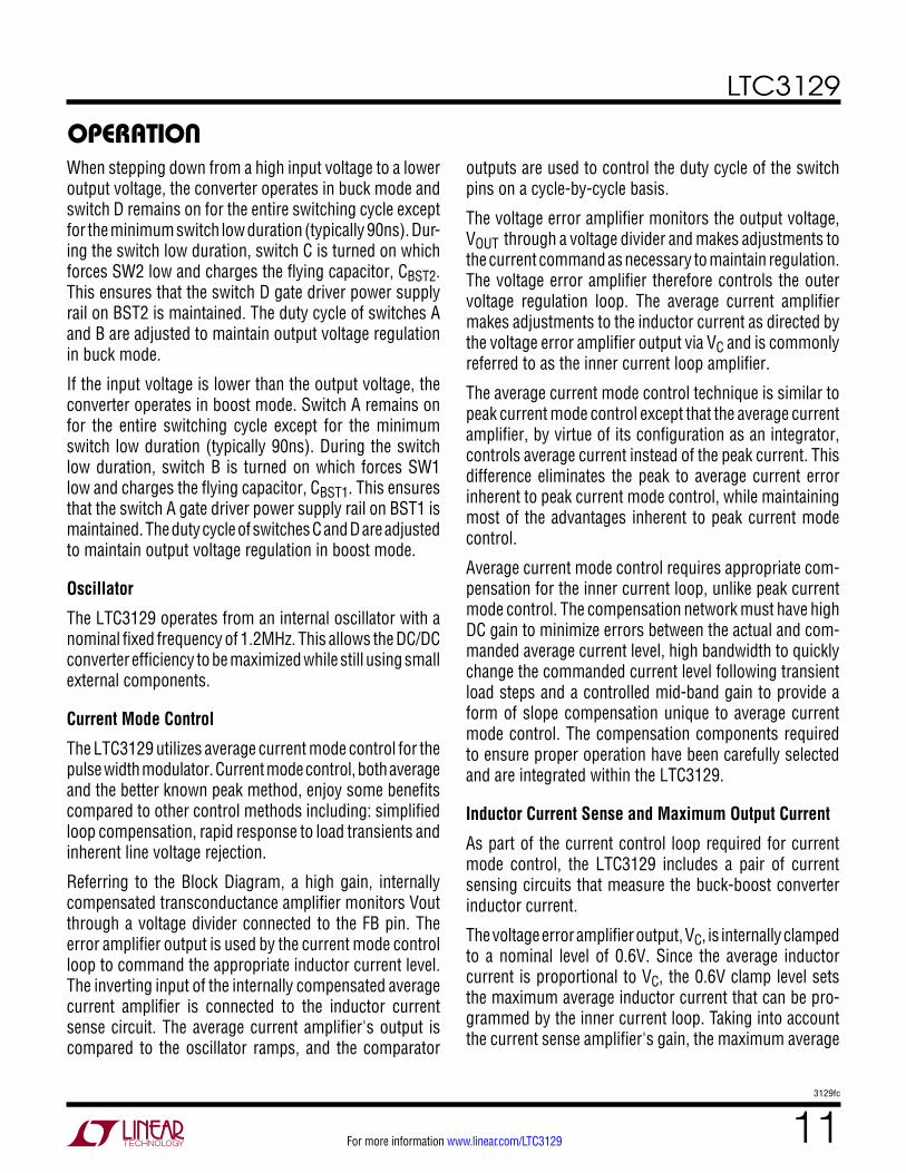
LTC3129
113129fc
For more information www.linear.com/LTC3129
operaTionWhen stepping down from a high input voltage to a lower output voltage, the converter operates in buck mode and switch D remains on for the entire switching cycle except for the minimum switch low duration (typically 90ns). Dur-ing the switch low duration, switch C is turned on which forces SW2 low and charges the flying capacitor, CBST2. This ensures that the switch D gate driver power supply rail on BST2 is maintained. The duty cycle of switches A and B are adjusted to maintain output voltage regulation in buck mode.
If the input voltage is lower than the output voltage, the converter operates in boost mode. Switch A remains on for the entire switching cycle except for the minimum switch low duration (typically 90ns). During the switch low duration, switch B is turned on which forces SW1 low and charges the flying capacitor, CBST1. This ensures that the switch A gate driver power supply rail on BST1 is maintained. The duty cycle of switches C and D are adjusted to maintain output voltage regulation in boost mode.
Oscillator
The LTC3129 operates from an internal oscillator with a nominal fixed frequency of 1.2MHz. This allows the DC/DC converter efficiency to be maximized while still using small external components.
Current Mode Control
The LTC3129 utilizes average current mode control for the pulse width modulator. Current mode control, both average and the better known peak method, enjoy some benefits compared to other control methods including: simplified loop compensation, rapid response to load transients and inherent line voltage rejection.
Referring to the Block Diagram, a high gain, internally compensated transconductance amplifier monitors Vout through a voltage divider connected to the FB pin. The error amplifier output is used by the current mode control loop to command the appropriate inductor current level. The inverting input of the internally compensated average current amplifier is connected to the inductor current sense circuit. The average current amplifier's output is compared to the oscillator ramps, and the comparator
outputs are used to control the duty cycle of the switch pins on a cycle-by-cycle basis.
The voltage error amplifier monitors the output voltage, VOUT through a voltage divider and makes adjustments to the current command as necessary to maintain regulation. The voltage error amplifier therefore controls the outer voltage regulation loop. The average current amplifier makes adjustments to the inductor current as directed by the voltage error amplifier output via VC and is commonly referred to as the inner current loop amplifier.
The average current mode control technique is similar to peak current mode control except that the average current amplifier, by virtue of its configuration as an integrator, controls average current instead of the peak current. This difference eliminates the peak to average current error inherent to peak current mode control, while maintaining most of the advantages inherent to peak current mode control.
Average current mode control requires appropriate com-pensation for the inner current loop, unlike peak current mode control. The compensation network must have high DC gain to minimize errors between the actual and com-manded average current level, high bandwidth to quickly change the commanded current level following transient load steps and a controlled mid-band gain to provide a form of slope compensation unique to average current mode control. The compensation components required to ensure proper operation have been carefully selected and are integrated within the LTC3129.
Inductor Current Sense and Maximum Output Current
As part of the current control loop required for current mode control, the LTC3129 includes a pair of current sensing circuits that measure the buck-boost converter inductor current.
The voltage error amplifier output, VC, is internally clamped to a nominal level of 0.6V. Since the average inductor current is proportional to VC, the 0.6V clamp level sets the maximum average inductor current that can be pro-grammed by the inner current loop. Taking into account the current sense amplifier's gain, the maximum average

LTC3129
123129fc
For more information www.linear.com/LTC3129
inductor current is approximately 275mA (typical). In Buck mode, the output current is approximately equal to the inductor current IL.
IOUT(BUCK) ≈ IL • 0.89
The 90ns SW1/SW2 forced low time on each switching cycle briefly disconnects the inductor from VOUT and VIN resulting in about 11% less output current in either buck or boost mode for a given inductor current. In boost mode, the output current is related to average inductor current and duty cycle by:
IOUT(BOOST) ≈ IL • (1 – D) • Efficiency,
where D is the converter duty cycle.
Since the output current in boost mode is reduced by the duty cycle (D), the output current rating in buck mode is always greater than in boost mode. Also, because boost mode operation requires a higher inductor current for a given output current compared to buck mode, the efficiency in boost mode will be lower due to higher IL² • RDS(ON) losses in the power switches. This will further reduce the output current capability in boost mode. In either operating mode, however, the inductor peak-to-peak ripple current does not play a major role in determining the output cur-rent capability, unlike peak current mode control.
With peak current mode control, the maximum output current capability is reduced by the magnitude of inductor ripple current because the peak inductor current level is the control variable, but the average inductor current is what determines the output current. The LTC3129 measures and controls average inductor current, and therefore, the inductor ripple current magnitude has little effect on the maximum current capability in contrast to an equivalent peak current mode converter. Under most conditions in buck mode, the LTC3129 is capable of providing a mini-mum of 200mA to the load. In boost mode, as described previously, the output current capability is related to the boost ratio or duty cycle (D). For example, for a 3.6V VIN to 5V output application, the LTC3129 can provide up to 150mA to the load. Refer to the Typical Performance characteristics section for more detail on output current capability.
operaTionOverload Current Limit and IZERO Comparator
The internal current sense waveform is also used by the peak overload current (IPEAK) and zero current (IZERO) com-parators. The IPEAK current comparator monitors Isense and turns off switch A if the inductor current level exceeds its maximum internal threshold, which is approximately 500mA. An inductor current level of this magnitude will occur during a fault, such as an output short-circuit, or during large load or input voltage transients.
The LTC3129 features near discontinuous inductor current operation at light output loads by virtue of the IZERO com-parator circuit. By limiting the reverse current magnitude in PWM mode, a balance between low noise operation and improved efficiency at light loads is achieved. The IZERO comparator threshold is set near the zero current level in PWM mode, and as a result, the reverse current magnitude will be a function of inductance value and output voltage due to the comparator's propagation delay. In general, higher output voltages and lower inductor values will result in increased reverse current magnitude.
In automatic Burst Mode operation (PWM pin low), the IZERO comparator threshold is increased so that reverse inductor current does not normally occur. This maximizes efficiency at very light loads.
Burst Mode OPERATION
When the PWM pin is held low, the LTC3129 is config-ured for automatic Burst Mode operation. As a result, the buck-boost DC/DC converter will operate with normal continuous PWM switching above a predetermined mini-mum output load and will automatically transition to power saving Burst Mode operation below this output load level. Note that if the PWM pin is low, reverse inductor current is not allowed at any load. Refer to the Typical Performance Characteristics section to determine the Burst Mode transition threshold for various combinations of VIN and VOUT. If PWM is low, at light output loads, the LTC3129 will go into a standby or sleep state when the output volt-age achieves its nominal regulation level. The sleep state halts PWM switching and powers down all non-essential

LTC3129
133129fc
For more information www.linear.com/LTC3129
operaTionfunctions of the IC, significantly reducing the quiescent current of the LTC3129 to just 1.3µA typical. This greatly improves overall power conversion efficiency when the output load is light. Since the converter is not operating in sleep, the output voltage will slowly decay at a rate determined by the output load resistance and the output capacitor value. When the output voltage has decayed by a small amount, typically 1%, the LTC3129 will wake and resume normal PWM switching operation until the volt-age on VOUT is restored to the previous level. If the load is very light, the LTC3129 may only need to switch for a few cycles to restore VOUT and may sleep for extended periods of time, significantly improving efficiency. If the load is suddenly increased above the burst transition threshold, the part will automatically resume continuous PWM operation until the load is once again reduced.
A feedforward capacitor on the feedback divider can be used to reduce Burst Mode VOUT ripple. This is discussed in more detail in the Applications Information section of this data sheet.
Note that Burst Mode operation is inhibited until soft-start is done, the MPPC pin is greater than 1.175V and VOUT has reached regulation.
Soft-Start
The LTC3129 soft-start circuit minimizes input current transients and output voltage overshoot on initial power up. The required timing components for soft-start are internal to the LTC3129 and produce a nominal soft-start dura-tion of approximately 3ms. The internal soft-start circuit slowly ramps the error amplifier output, VC. In doing so, the current command of the IC is also slowly increased, starting from zero. It is unaffected by output loading or output capacitor value. Soft-start is reset by the UVLO on both VIN and VCC, the RUN pin and thermal shutdown.
VCC Regulator
An internal low dropout regulator (LDO) generates a nomi-nal 4.1V VCC rail from VIN. The VCC rail powers the internal control circuitry and the gate drivers of the LTC3129. The VCC regulator is disabled in shutdown to reduce quiescent current and is enabled by raising the RUN pin above its
logic threshold. The VCC regulator includes current-limit protection to safeguard against accidental short-circuiting of the VCC rail.
Undervoltage Lockout (UVLO)
There are two undervoltage lockout (UVLO) circuits within the LTC3129 that inhibit switching; one that monitors VIN and another that monitors VCC. Either UVLO will disable operation of the internal power switches and keep other IC functions in a reset state if either VIN or VCC are below their respective UVLO thresholds.
The VIN UVLO comparator has a falling voltage threshold of 1.8V (typical). If VIN falls below this level, IC operation is disabled until VIN rises above 1.9V (typical), as long as the VCC voltage is above its UVLO threshold.
The VCC UVLO has a falling voltage threshold of 2.19V (typical). If the VCC voltage falls below this threshold, IC operation is disabled until VCC rises above 2.25V (typical) as long as VIN is above its nominal UVLO threshold level.
Depending on the particular application, either of these UVLO thresholds could be the limiting factor affecting the minimum input voltage required for operation. Because the VCC regulator uses VIN for its power input, the minimum input voltage required for operation is determined by the VCC minimum voltage, as input voltage (VIN) will always be higher than VCC in the normal (non-bootstrapped) configuration. Therefore, the minimum VIN for the part to startup is 2.25V (typical).
In applications where VCC is bootstrapped (powered through a Schottky diode by either VOUT or an auxiliary power rail), the minimum input voltage for operation will be limited only by the VIN UVLO threshold (1.8V typical). Please note that if the bootstrap voltage is derived from the LTC3129 VOUT and not an independent power rail, then the minimum input voltage required for initial startup is still 2.25V (typical).
Note that if either VIN or VCC are below their UVLO thresh-olds, or if RUN is below its accurate threshold of 1.22V (typical), then the LTC3129 will remain in a soft shutdown state, where the VIN quiescent current will be only 1.9µA typical.

LTC3129
143129fc
For more information www.linear.com/LTC3129
operaTionVOUT Undervoltage
There is also an undervoltage comparator that monitors the output voltage. Until VOUT reaches 1.15V (typical), the average current limit is reduced by a factor of two. This reduces power dissipation in the device in the event of a shorted output. In addition, N-channel switch D, which feeds VOUT, will be disabled until VOUT exceeds 1.15V.
RUN Pin Comparator
In addition to serving as a logic level input to enable cer-tain functions of the IC, the RUN pin includes an accurate internal comparator that allows it to be used to set custom rising and falling ON/OFF thresholds with the addition of an optional external resistor divider. When RUN is driven above its logic threshold (0.9V typical), the VCC regulator is enabled, which provides power to the internal control circuitry of the IC. If the voltage on RUN is increased further so that it exceeds the RUN comparator's accurate analog threshold (1.22V typical), all functions of the buck-boost converter will be enabled and a start-up sequence will ensue, assuming the VIN and VCC UVLO thresholds are satisfied.
If RUN is brought below the accurate comparator threshold, the buck-boost converter will inhibit switching, but the VCC regulator and control circuitry will remain powered unless RUN is brought below its logic threshold. Therefore, in order to completely shut down the IC and reduce the Vin current to 10nA (typical), it is necessary to ensure that RUN is brought below its worst case low logic threshold of 0.5V. RUN is a high voltage input and can be tied directly to VIN to continuously enable the IC when the input supply is present. Also note that RUN can be driven above VIN or VOUT as long as it stays within the operating range of the IC (up to 15V).
With the addition of an optional resistor divider as shown in Figure 2, the RUN pin can be used to establish a user-programmable turn-on and turn-off threshold. This feature can be utilized to minimize battery drain below a certain input voltage, or to operate the converter in a hiccup mode from very low current sources.
Figure 2. Accurate RUN Pin Comparator
LTC3129
ENABLE SWITCHING
ENABLE LDO AND CONTROL CIRCUITS
LOGIC THRESHOLD
ACCURATE THRESHOLD
3129 F02
+–
–+
0.9V
RUN
1.22VVIN
R3
R4
Note that once RUN is above 0.9V typical, the quiescent input current on VIN (or VCC if back-driven) will increase to about 1.9µA typical until the VIN and VCC UVLO thresholds are satisfied.
The converter is enabled when the voltage on RUN exceeds 1.22V (nominal). Therefore, the turn-on voltage threshold on VIN is given by:
VIN(TURN-ON) = 1.22V • (1 + R3/R4)
The RUN comparator includes a built-in hysteresis of approximately 80mV, so that the turn off threshold will be 1.14V.
There may be cases due to PCB layout, very large value resistors for R3 and R4, or proximity to noisy components where noise pickup may cause the turn-on or turn-off of the IC to be intermittent. In these cases, a small filter capacitor can be added across R4 to ensure proper operation.

LTC3129
153129fc
For more information www.linear.com/LTC3129
operaTionPGOOD Comparator
The LTC3129 provides an open-drain PGOOD output that pulls low if VOUT falls more than 7.5% (typical) below its programmed value. When VOUT rises to within 5% (typical) of its programmed value, the internal PGOOD pull-down will turn off and PGOOD will go high if an external pull-up resistor has been provided. An internal filter prevents nuisance trips of PGOOD due to short transients on VOUT. Note that PGOOD can be pulled up to any voltage, as long as the absolute maximum rating of 18V is not exceeded, and as long as the maximum sink current rating is not exceeded when PGOOD is low. Note that PGOOD will also be driven low if VCC is below its UVLO threshold or if the part is in shutdown (RUN below its logic threshold) while VCC is being held up (or back-driven). PGOOD is not affected by VIN UVLO or the accurate RUN threshold.
In cases where VCC is not being back-driven in shutdown, PGOOD will not be held low indefinitely. The internal PGOOD pull-down will be disabled as the VCC voltage decays below approximately 1V.
Maximum Power-Point Control (MPPC)
The MPPC input of the LTC3129 can be used with an optional external voltage divider to dynamically adjust
the commanded inductor current in order to maintain a minimum input voltage when using high resistance sources, such as photovoltaic panels, so as to maximize input power transfer and prevent VIN from dropping too low under load. Referring to Figure 3, the MPPC pin is internally connected to the non-inverting input of a gm amplifier, whose inverting input is connected to the 1.175V reference. If the voltage at MPPC, using the external volt-age divider, falls below the reference voltage, the output of the amplifier pulls the internal VC node low. This reduces the commanded average inductor current so as to reduce the input current and regulate VIN to the programmed minimum voltage, as given by:
VIN(MPPC) = 1.175V • (1 + R5/R6)
The MPPC feature provides capabilities to the LTC3129 that can ease the design of intrinsically safe power supplies.
Note that external compensation should not be required for MPPC loop stability if input filter capacitor, CIN, is at least 22µF.
The divider resistor values can be in the MΩ range to minimize the input current in very low power applications. However, stray capacitance and noise pickup on the MPPC pin must also be minimized.
Figure 3. MPPC Amplifier with External Resistor Divider
LTC3129
1.175V
VCCURRENTCOMMAND
VOLTAGEERROR AMP
3129 F03
MPPC
FB
R5
R6
RS
VSOURCE
*CIN
* CIN SHOULD BE AT LEAST 22µF FOR MPPC APPLICATIONS
VIN
+–
+–
+
–
LTC3129
163129fc
For more information www.linear.com/LTC3129
operaTion
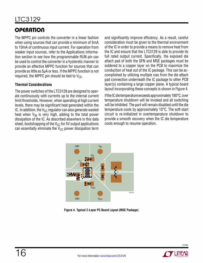
Figure 4. Typical 2-Layer PC Board Layout (MSE Package)
The MPPC pin controls the converter in a linear fashion when using sources that can provide a minimum of 5mA to 10mA of continuous input current. For operation from weaker input sources, refer to the Applications Informa-tion section to see how the programmable RUN pin can be used to control the converter in a hysteretic manner to provide an effective MPPC function for sources that can provide as little as 5µA or less. If the MPPC function is not required, the MPPC pin should be tied to VCC.
Thermal Considerations
The power switches of the LTC3129 are designed to oper-ate continuously with currents up to the internal current limit thresholds. However, when operating at high current levels, there may be significant heat generated within the IC. In addition, the VCC regulator can also generate wasted heat when VIN is very high, adding to the total power dissipation of the IC. As described elsewhere in this data sheet, bootstrapping of the VCC for 5V output applications can essentially eliminate the VCC power dissipation term
and significantly improve efficiency. As a result, careful consideration must be given to the thermal environment of the IC in order to provide a means to remove heat from the IC and ensure that the LTC3129 is able to provide its full rated output current. Specifically, the exposed die attach pad of both the QFN and MSE packages must be soldered to a copper layer on the PCB to maximize the conduction of heat out of the IC package. This can be ac-complished by utilizing multiple vias from the die attach pad connection underneath the IC package to other PCB layer(s) containing a large copper plane. A typical board layout incorporating these concepts is shown in Figure 4.
If the IC die temperature exceeds approximately 180°C, over temperature shutdown will be invoked and all switching will be inhibited. The part will remain disabled until the die temperature cools by approximately 10°C. The soft-start circuit is re-initialized in overtemperature shutdown to provide a smooth recovery when the IC die temperature cools enough to resume operation.
GND VIN
VCC
GND VOUT
COUT
CIN
L
3129 F04
LTC3129
173129fc
For more information www.linear.com/LTC3129
applicaTions inForMaTionA standard application circuit for the LTC3129 is shown on the front page of this data sheet. The appropriate selection of external components is dependent upon the required performance of the IC in each particular application given considerations and trade-offs such as PCB area, input and output voltage range, output voltage ripple, transient response, required efficiency, thermal considerations and cost. This section of the data sheet provides some basic guidelines and considerations to aid in the selection of external components and the design of the applications circuit, as well as more application circuit examples.
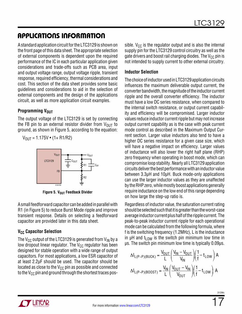
Programming VOUT
The output voltage of the LTC3129 is set by connecting the FB pin to an external resistor divider from VOUT to ground, as shown in Figure 5, according to the equation:
VOUT = 1.175V • (1+ R1/R2)
sible. VCC is the regulator output and is also the internal supply pin for the LTC3129 control circuitry as well as the gate drivers and boost rail charging diodes. The VCC pin is not intended to supply current to other external circuitry.
Inductor Selection
The choice of inductor used in LTC3129 application circuits influences the maximum deliverable output current, the converter bandwidth, the magnitude of the inductor current ripple and the overall converter efficiency. The inductor must have a low DC series resistance, when compared to the internal switch resistance, or output current capabil-ity and efficiency will be compromised. Larger inductor values reduce inductor current ripple but may not increase output current capability as is the case with peak current mode control as described in the Maximum Output Cur-rent section. Larger value inductors also tend to have a higher DC series resistance for a given case size, which will have a negative impact on efficiency. Larger values of inductance will also lower the right half plane (RHP) zero frequency when operating in boost mode, which can compromise loop stability. Nearly all LTC3129 application circuits deliver the best performance with an inductor value between 3.3µH and 10µH. Buck mode-only applications can use the larger inductor values as they are unaffected by the RHP zero, while mostly boost applications generally require inductance on the low end of this range depending on how large the step-up ratio is.
Regardless of inductor value, the saturation current rating should be selected such that it is greater than the worst-case average inductor current plus half of the ripple current. The peak-to-peak inductor current ripple for each operational mode can be calculated from the following formula, where f is the switching frequency (1.2MHz), L is the inductance in µH and tLOW is the switch pin minimum low time in µs. The switch pin minimum low time is typically 0.09µs.
ΔIL(P−P)(BUCK) =VOUT
LVIN – VOUT
VIN
⎛
⎝⎜
⎞
⎠⎟
1f
– tLOW⎛
⎝⎜
⎞
⎠⎟ A
ΔIL(P−P)(BOOST) =VINL
VOUT – VINVOUT
⎛
⎝⎜
⎞
⎠⎟
1f
– tLOW⎛
⎝⎜
⎞
⎠⎟ A
Figure 5. VOUT Feedback Divider
A small feedforward capacitor can be added in parallel with R1 (in Figure 5) to reduce Burst Mode ripple and improve transient response. Details on selecting a feedforward capacitor are provided later in this data sheet.
VCC Capacitor Selection
The VCC output of the LTC3129 is generated from VIN by a low dropout linear regulator. The VCC regulator has been designed for stable operation with a wide range of output capacitors. For most applications, a low ESR capacitor of at least 2.2µF should be used. The capacitor should be located as close to the VCC pin as possible and connected to the VCC pin and ground through the shortest traces pos-
3129 F05
LTC3129
VOUT VOUT
R1COUT
FB
CFF
R2
LTC3129
183129fc
For more information www.linear.com/LTC3129
It should be noted that the worst-case peak-to-peak in-ductor ripple current occurs when the duty cycle in buck mode is minimum (highest VIN) and in boost mode when the duty cycle is 50% (VOUT = 2 • VIN). As an example, if VIN (minimum) = 2.5V and VIN (maximum) = 15V, VOUT = 5V and L = 10µH, the peak-to-peak inductor ripples at the voltage extremes (15V VIN for buck and 2.5V VIN for boost) are:
Buck = 248mA peak-to-peak
Boost = 93mA peak-to-peak
One half of this inductor ripple current must be added to the highest expected average inductor current in order to select the proper saturation current rating for the inductor.
To avoid the possibility of inductor saturation during load transients, an inductor with a saturation current rating of at least 600mA is recommended for all applications.
In addition to its influence on power conversion efficiency, the inductor DC resistance can also impact the maximum output current capability of the buck-boost converter particularly at low input voltages. In buck mode, the output current of the buck-boost converter is primarily limited by the inductor current reaching the average cur-rent limit threshold. However, in boost mode, especially at large step-up ratios, the output current capability can also be limited by the total resistive losses in the power stage. These losses include, switch resistances, inductor DC resistance and PCB trace resistance. Avoid inductors with a high DC resistance (DCR) as they can degrade the maximum output current capability from what is shown in the Typical Performance Characteristics section and from the Typical Application circuits.
As a guideline, the inductor DCR should be significantly less than the typical power switch resistance of 750mΩ each. The only exceptions are applications that have a maximum output current requirement much less than what the LTC3129 is capable of delivering. Generally speaking, inductors with a DCR in the range of 0.15Ω to 0.3Ω are recommended. Lower values of DCR will improve the ef-ficiency at the expense of size, while higher DCR values will reduce efficiency (typically by a few percent) while allowing the use of a physically smaller inductor.
applicaTions inForMaTionDifferent inductor core materials and styles have an impact on the size and price of an inductor at any given current rating. Shielded construction is generally preferred as it minimizes the chances of interference with other circuitry. The choice of inductor style depends upon the price, sizing, and EMI requirements of a particular application. Table 1 provides a wide sampling of inductors that are well suited to many LTC3129 applications.
Table 1. Recommended InductorsVENDOR PART
Coilcraft www.coilcraft.com
EPL2014, EPL3012, EPL3015, LPS3015, LPS3314, XFL3012
Coiltronics www.cooperindustries.com
SDH3812, SD3814, SD3114, SD3118
Murata www.murata.com
LQH3NP, LQH32P, LQH44P
Sumida www.sumida.com
CDRH2D16, CDRH2D18, CDRH3D14, CDRH3D16
Taiyo-Yuden www.t-yuden.com
NR3012T, NR3015T, NRS4012T, BRC2518
TDK www.tdk.com
VLS3012, VLS3015, VLF302510MT, VLF302512MT
Toko www.tokoam.com
DB3015C, DB3018C, DB3020C, DP418C, DP420C, DEM2815C, DFE322512C, DFE252012C
Würth www.we-online.com
WE-TPC 2813, WE-TPC 3816, WE-TPC 2828
Recommended inductor values for different operating voltage ranges are given in Table 2. These values were chosen to minimize inductor size while maintaining an acceptable amount of inductor ripple current for a given VIN and VOUT range.
Table 2. Recommended Inductor ValuesVIN AND VOUT RANGE RECOMMENDED INDUCTOR VALUES
VIN and VOUT Both < 4.5V 3.3µH to 4.7µH
VIN and VOUT Both < 8V 4.7µH to 6.8µH
VIN and VOUT Both < 11V 6.8µH to 8.2µH
VIN and VOUT Up to 15.75V 8.2µH to 10µH
Feedforward Capacitor
The use of a voltage feedforward capacitor, as shown in Figure 5, offers a number of performance advantages. A feedforward capacitor will reduce output voltage ripple in
LTC3129
193129fc
For more information www.linear.com/LTC3129
applicaTions inForMaTionExamining the previous equations reveals that the output voltage ripple increases with load current and is gener-ally higher in boost mode than in buck mode. Note that these equations only take into account the voltage ripple that occurs from the inductor current to the output being discontinuous. They provide a good approximation to the ripple at any significant load current but underestimate the output voltage ripple at very light loads where the output voltage ripple is dominated by the inductor current ripple.
In addition to the output voltage ripple generated across the output capacitance, there is also output voltage ripple produced across the internal resistance of the output capacitor. The ESR-generated output voltage ripple is proportional to the series resistance of the output capacitor and is given by the following expressions where RESR is the series resistance of the output capacitor and all other terms as previously defined.
ΔVP−P(BUCK) =ILOADRESR
1– tLOWf≅ ILOADRESR V
ΔVP−P(BOOST) =ILOADRESRVOUT
VIN 1– tLOWf( )≅ ILOADRESR
VOUTVIN
⎛
⎝⎜
⎞
⎠⎟ V
In most LTC3129 applications, an output capacitor between 10µF and 22µF will work well. To minimize output ripple in Burst Mode operation, or transients incurred by large step loads, values of 22µF or larger are recommended.
Input Capacitor Selection
The VIN pin carries the full inductor current and provides power to internal control circuits in the IC. To minimize input voltage ripple and ensure proper operation of the IC, a low ESR bypass capacitor with a value of at least 4.7µF should be located as close to the VIN pin as possible. The traces connecting this capacitor to VIN and the ground plane should be made as short as possible.
Burst Mode operation and improve transient response. In addition, due to the wide VIN and VOUT operating range of the LTC3129 and its fixed internal loop compensation, some applications may require the use of a feedforward capacitor to assure light-load stability (less than ~15mA) when operating in PWM mode (PWM pin pulled high).
Therefore, to reduce Burst Mode ripple and improve phase margin at light load when PWM mode operation is selected, a feedforward capacitor is recommended for all applications. The recommended feedforward capacitor value can be calculated by:
CFF = 66/R1
Where R1 is the top feedback divider resistor value in MΩ and CFF is the recommended feedforward capacitor value in picofarads (use the nearest standard value). Refer to the application circuits for examples.
Output Capacitor Selection
A low effective series resistance (ESR) output capacitor of 4.7µF minimum should be connected at the output of the buck-boost converter in order to minimize output volt-age ripple. Multilayer ceramic capacitors are an excellent option as they have low ESR and are available in small footprints. The capacitor value should be chosen large enough to reduce the output voltage ripple to acceptable levels. Neglecting the capacitor's ESR and ESL (effec-tive series inductance), the peak-to-peak output voltage ripple in PWM mode can be calculated by the following formula, where f is the frequency in MHz (1.2MHz), COUT is the capacitance in µF, tLOW is the switch pin minimum low time in µs (0.09µs typical) and ILOAD is the output current in amperes.
ΔVP−P(BUCK) =ILOADtLOW
COUTV
ΔVP−P(BOOST) =ILOAD
fCOUT
VOUT – VIN + tLOWfVIN
VOUT
⎛
⎝⎜
⎞
⎠⎟ V
LTC3129
203129fc
For more information www.linear.com/LTC3129
When powered through long leads or from a power source with significant resistance, a larger value bulk input capacitor may be required and is generally recommended. In such applications, a 47µF to 100µF low-ESR electrolytic capacitor in parallel with a 1µF ceramic capacitor generally yields a high performance, low cost solution.
Note that applications using the MPPC feature should use a minimum CIN of 22µF. Larger values can be used without limitation.
Recommended Input and Output Capacitor Types
The capacitors used to filter the input and output of the LTC3129 must have low ESR and must be rated to handle the AC currents generated by the switching converter. This is important to maintain proper functioning of the IC and to reduce output voltage ripple. There are many capacitor types that are well suited to these applications including multilayer ceramic, low ESR tantalum, OS-CON and POSCAP technologies. In addition, there are certain types of electrolytic capacitors such as solid aluminum organic polymer capacitors that are designed for low ESR and high AC currents and these are also well suited to some LTC3129 applications. The choice of capacitor technology is primarily dictated by a trade-off between size, leakage current and cost. In backup power applica-tions, the input or output capacitor might be a super or ultra capacitor with a capacitance value measuring in the Farad range. The selection criteria in these applications are generally similar except that voltage ripple is generally not a concern. Some capacitors exhibit a high DC leak-age current which may preclude their consideration for applications that require a very low quiescent current in Burst Mode operation. Note that ultra capacitors may have a rather high ESR, therefore a 4.7µF (minimum) ceramic capacitor is recommended in parallel, close to the IC pins.
Ceramic capacitors are often utilized in switching con-verter applications due to their small size, low ESR and low leakage currents. However, many ceramic capacitors intended for power applications experience a significant loss in capacitance from their rated value as the DC bias voltage on the capacitor increases. It is not uncommon for a small surface mount capacitor to lose more than 50%
of its rated capacitance when operated at even half of its maximum rated voltage. This effect is generally reduced as the case size is increased for the same nominal value capacitor. As a result, it is often necessary to use a larger value capacitance or a higher voltage rated capacitor than would ordinarily be required to actually realize the intended capacitance at the operating voltage of the application. X5R and X7R dielectric types are recommended as they exhibit the best performance over the wide operating range and temperature of the LTC3129. To verify that the intended capacitance is achieved in the application circuit, be sure to consult the capacitor vendor's curve of capacitance versus DC bias voltage.
Using the Programmable RUN Function to Operate from Extremely Weak Input Sources
Another application of the programmable RUN pin is that it can be used to operate the converter in a hiccup mode from extremely low current sources. This allows operation from sources that can only generate microamps of output current, and would be far too weak to sustain normal steady-state operation, even with the use of the MPPC pin. Because the LTC3129 draws only 1.9µA typical from VIN until it is enabled, the RUN pin can be programmed to keep the IC disabled until VIN reaches the programmed voltage level. In this manner, the input source can trickle-charge an input storage capacitor, even if it can only supply microamps of current, until VIN reaches the turn-on threshold set by the RUN pin divider. The converter will then be enabled using the stored charge in the input capacitor, until Vin drops below the turn-off threshold, at which point the converter will turn off and the process will repeat.
This approach allows the converter to run from weak sources such as thin-film solar cells using indoor lighting. Although the converter will be operating in bursts, it is enough to charge an output capacitor to power low duty cycle loads, such as wireless sensor applications, or to trickle charge a battery. In addition, note that the input voltage will be cycling (with a small ripple as set by the RUN hysteresis) about a fixed voltage, as determined by the divider. This allows the high impedance source to operate at the programmed optimal voltage for maximum power transfer.
applicaTions inForMaTion

LTC3129
213129fc
For more information www.linear.com/LTC3129
applicaTions inForMaTionWhen using high value divider resistors (in the MΩ range) to minimize current draw on VIN, a small noise filter capacitor may be necessary across the lower divider resistor to prevent noise from erroneously tripping the RUN comparator. The capacitor value should be minimized so as not to introduce a time delay long enough for the input voltage to drop significantly below the desired VIN threshold before the converter is turned off. Note that larger VIN decoupling capacitor values will minimize this effect by providing more holdup time on VIN.
Programming the MPPC Voltage
As discussed in the previous section, the LTC3129 in-cludes an MPPC function to optimize performance when operating from voltage sources with relatively high source resistance. Using an external voltage divider from VIN, the MPPC function takes control of the average inductor current when necessary to maintain a minimum input voltage, as programmed by the user. Referring to Figure 3:
VIN(MPPC) = 1.175V • (1 + R5/R6)
This is useful for such applications as photovoltaic pow-ered converters, since the maximum power transfer point occurs when the photovoltaic panel is operated at about 75% of its open-circuit voltage. For example, when operat-ing from a photovoltaic panel with an open-circuit voltage of 5V, the maximum power transfer point will be when the panel is loaded such that its output voltage is about 3.75V. Choosing values of 2MΩ for R5 and 909kΩ for R6 will program the MPPC function to regulate the maximum input current so as to maintain VIN at a minimum of 3.74V (typical). Note that if the panel can provide more power than the LTC3129 can draw, the input voltage will rise above the programmed MPPC point. This is fine as long as the input voltage doesn't exceed 15V.
For weak input sources with very high resistance (hun-dreds of Ohms or more), the LTC3129 may still draw more current than the source can provide, causing VIN to drop below the UVLO threshold. For these applications, it is recommended that the programmable RUN feature be used, as described in the previous section.
MPPC Compensation and Gain
When using MPPC, there are a number of variables that affect the gain and phase of the input voltage control loop. Primarily these are the input capacitance, the MPPC divider ratio and the VIN source resistance (or current). To simplify the design of the application circuit, the MPPC control loop in the LTC3129 is designed with a relatively low gain, such that external MPPC loop compensation is generally not required when using a VIN capacitor value of at least 22µF. The gain from the MPPC pin to the in-ternal VC control voltage is about 12, so a drop of 50mV on the MPPC pin (below the 1.175V MPPC threshold), corresponds to a 600mV drop on the internal VC voltage, which reduces the average inductor current all the way to zero. Therefore, the programmed input MPPC voltage will be maintained within about 4% over the load range.
Note that if large value VIN capacitors are used (which may have a relatively high ESR) a small ceramic capacitor of at least 4.7µF should be placed in parallel across the VIN input, near the VIN pin of the IC.
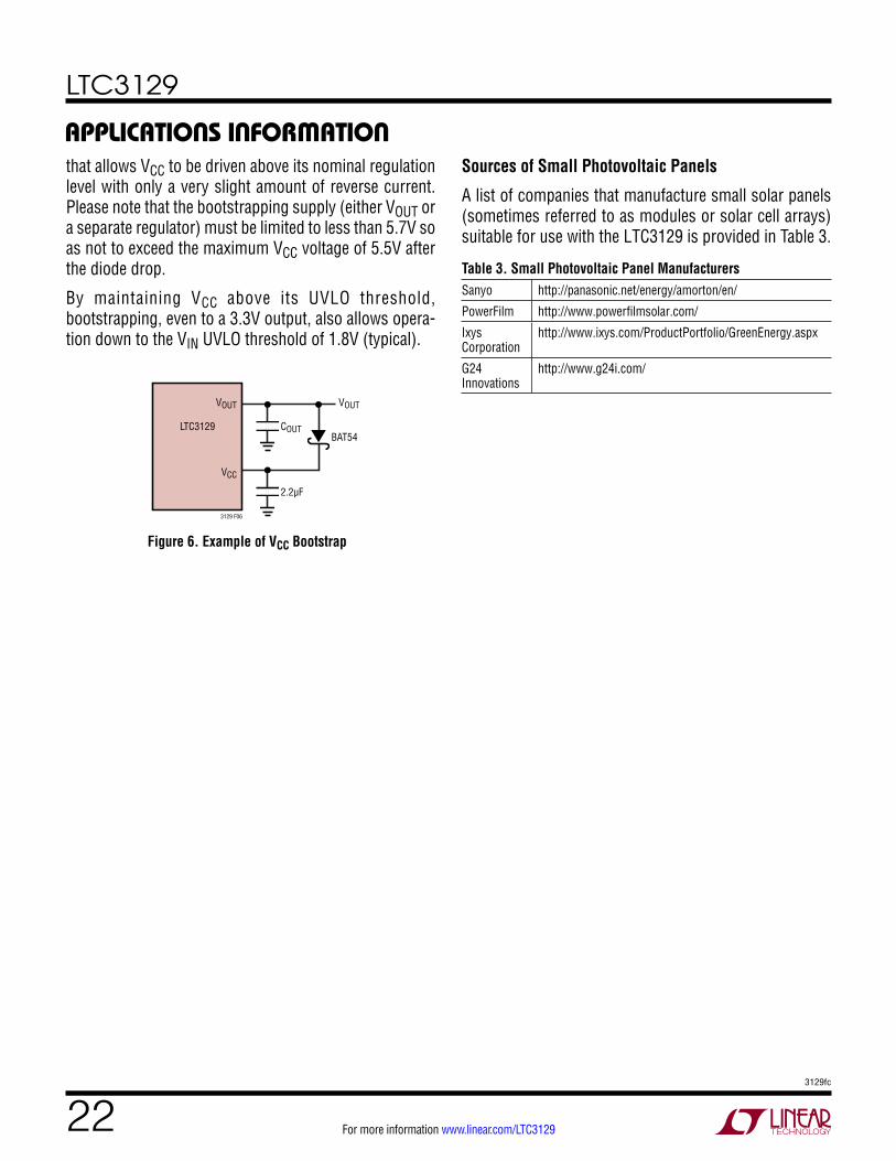
Bootstrapping the VCC Regulator
The high and low side gate drivers are powered through the VCC rail, which is generated from the input voltage, VIN, through an internal linear regulator. In some applications, especially at high input voltages, the power dissipation in the linear regulator can become a major contributor to thermal heating of the IC and overall efficiency. The Typical Performance Characteristics section provides data on the VCC current and resulting power loss versus VIN and VOUT.
A significant performance advantage can be attained in high VIN applications where converter output voltage (VOUT) is programmed to 5V, if VOUT is used to power the VCC rail. Powering VCC in this manner is referred to as bootstrapping. This can be done by connecting a Schottky diode (such as a BAT54) from VOUT to VCC as shown in Figure 6. With the bootstrap diode installed, the gate driver currents are supplied by the buck-boost converter at high efficiency rather than through the internal linear regulator. The in-ternal linear regulator contains reverse blocking circuitry
LTC3129
223129fc
For more information www.linear.com/LTC3129
that allows VCC to be driven above its nominal regulation level with only a very slight amount of reverse current. Please note that the bootstrapping supply (either VOUT or a separate regulator) must be limited to less than 5.7V so as not to exceed the maximum VCC voltage of 5.5V after the diode drop.
By maintaining VCC above its UVLO threshold, bootstrapping, even to a 3.3V output, also allows opera-tion down to the VIN UVLO threshold of 1.8V (typical).
Sources of Small Photovoltaic Panels
A list of companies that manufacture small solar panels (sometimes referred to as modules or solar cell arrays) suitable for use with the LTC3129 is provided in Table 3.
Table 3. Small Photovoltaic Panel ManufacturersSanyo http://panasonic.net/energy/amorton/en/
PowerFilm http://www.powerfilmsolar.com/
Ixys Corporation
http://www.ixys.com/ProductPortfolio/GreenEnergy.aspx
G24 Innovations
http://www.g24i.com/
applicaTions inForMaTion
Figure 6. Example of VCC Bootstrap
3129 F06
LTC3129
VOUT VOUT
BAT54COUT
VCC
2.2µF

LTC3129
233129fc
For more information www.linear.com/LTC3129
Typical applicaTions
Low Noise 3.6V Converter Using Bootstrap Diode to Extend Lower VIN Range
Hiccup Converter Powers Wireless Sensor from Indoor LightingTransmit Rate vs Light Level
(Fluorescent)
LIGHT LEVEL (Lx)0
TRAN
SMIT
RAT
E (H
z)
4.5
4.0
2.0
3.5
3.0
2.5
1.5
1.0
0.5
0
3129 TA02b
2000800 1200 1600400
BST1VOUT
VOUT3.6V
SW1 SW2
LTC3129
22nF
BST2
PGOOD
FB
GND
VCC
VINVIN
1.8V TO 15V
RUN
MPPC
PWM
VCC
NC
NC
22nF 6.8µH
2M BAT54
976k
10µF
10µF
33pF
2.2µF
3129 TA03
PGND
VIN < 3.6V, IOUT = 100mAVIN > 3.6V, IOUT = 200mA
BST1VOUT
VOUT3.6V
SW1 SW2
LTC3129
22nF
BST2
PGOOD
FB
PGOOD
GND
VCC
VINVIN UVLO = 3.5V
RUN
MPPC
PWM
VCC
NC
NC
22nF 4.7µH
1M2M
976k
2.37M
4.42M
470µF6.3V
+
10pF
22µF4.7µF
2.2µF
3129 TA02a
PGND
PV PANELSANYO AM-1815
4.9cm × 5.8cm
PULSED IOUT25mA FOR 5ms

LTC3129
243129fc
For more information www.linear.com/LTC3129
Typical applicaTionsSolar Powered Converter with MPPC Charges Storage Capacitor
Average Output Currentvs Light Level (Daylight)
BST1VOUT
VOUT4.8V
PGOOD
SW1 SW2
LTC3129
22nF
BST2
PGOOD
FB
GND
VCC
VINVIN
UVLO = 4.3V
RUN
MPPC
PWM
NC
NC
22nF 4.7µH
1M
VCC
392k
8.4cm × 3.7cm
47µFCERAMIC
4.7µF 1F3.09M
2.2µF
3129 TA04a
PGND
PowerFilmSP4.2-37SOLAR
MODULE
1M
+
COOPER BUSSMANNPB-5R0V105-R
LIGHT LEVEL (Lx)1000
OUTP
UT C
URRE
NT (m
A)
100.0
10.0
1.0
0.1
3129 TA04b
100000010000010000
LTC3129
253129fc
For more information www.linear.com/LTC3129
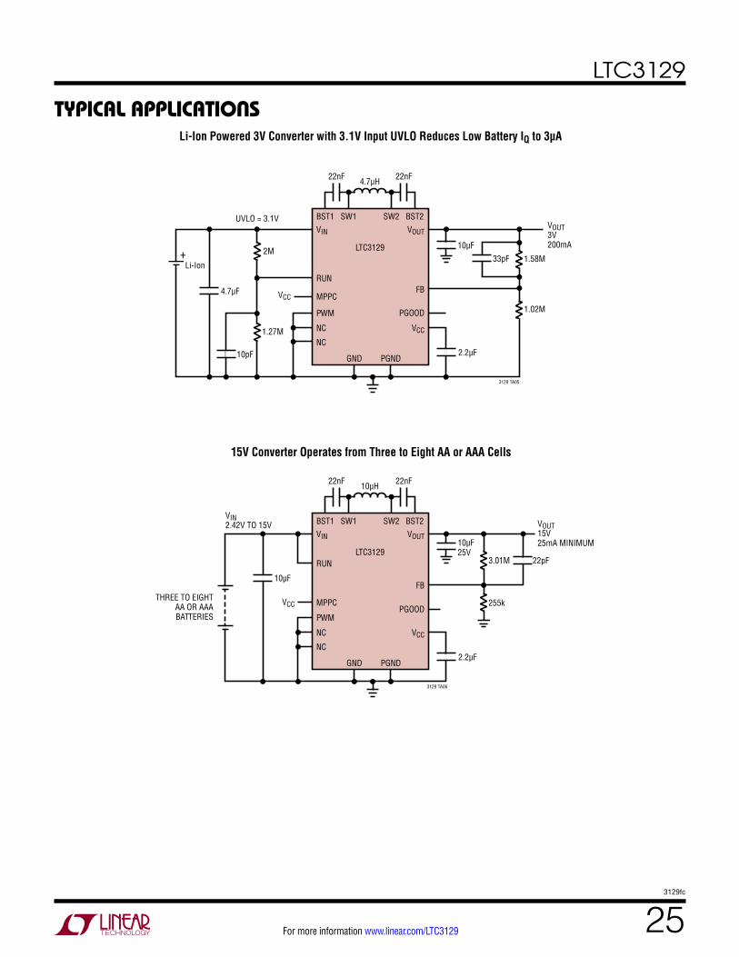
Li-Ion Powered 3V Converter with 3.1V Input UVLO Reduces Low Battery IQ to 3µA
15V Converter Operates from Three to Eight AA or AAA Cells
Typical applicaTions
BST1VOUT
VOUT3V200mA
SW1 SW2
LTC3129
22nF
BST2
PGOOD
FB
GND
VCC
VCC
VIN
Li-Ion+
RUN
MPPC
PWM
NC
NC
22nF 4.7µH
2M
UVLO = 3.1V
1.27M
4.7µF
10pF
10µF
33pF 1.58M
2.2µF
3129 TA05
PGND
1.02M
VCC
BST1VOUT
VOUT15V25mA MINIMUM
SW1 SW2
LTC3129
22nF
BST2
PGOOD
FB
GND
VCC
VIN
VIN2.42V TO 15V
RUN
22nF 10µH
10µF25V
3.01M
2.2µF
3129 TA06
PGND
THREE TO EIGHTAA OR AAABATTERIES
MPPC
PWM
NC
NC
10µF
255k
22pF
LTC3129
263129fc
For more information www.linear.com/LTC3129
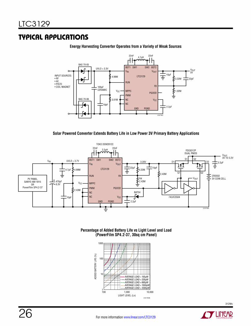
Typical applicaTionsEnergy Harvesting Converter Operates from a Variety of Weak Sources
Solar Powered Converter Extends Battery Life in Low Power 3V Primary Battery Applications
Percentage of Added Battery Life vs Light Level and Load (PowerFilm SP4.2-37, 30sq cm Panel)
LIGHT LEVEL (Lx)100
ADDE
D BA
TTER
Y LI
FE (%
)
1000
100
10
1
3129 TA09b
10,0001,000
AVERAGE LOAD = 165µWAVERAGE LOAD = 330µWAVERAGE LOAD = 660µWAVERAGE LOAD = 1650µWAVERAGE LOAD = 3300µW
VCC
BST1VOUT
VOUT5V
SW1 SW2
LTC3129
22nF
BST2
PGOOD
FB
GND
VCC
VIN
BAS 70-05
UVLO = 3.3V
RUN
22nF 4.7µH
10µF
3.32M
2.2µF
3129 TA07
PGND
MPPC
PWM
NC
NC
100µFCERAMIC 1.02M
4.99M
3.01MBAS 70-06
INPUT SOURCES:• RF• AC• PIEZO• COIL-MAGNET
10pF
22pF
BST1VOUT
SW1 SW2
LTC3129
22nF
3.20VBST2
PGOOD
FB
GND
VCC
VCC
VIN
RUN
MPPC
PWM
NC
NC
22nF 3.3µH
TOKO DEM2812C
10pF
2.2µF
VOUT
BAT54
470µF6.3V
74LVC2G04
3129 TA09
PGND
FDC6312PDUAL PMOS
PV PANELSANYO AM-1815
ORPowerFilm SP4.2-37
4.7µF
VIN UVLO = 3.7V
4.99M 4.22M
2.43M
D1 D2S2S1
G2CR20323V COIN CELL
VOUT3V TO 3.2V
G1
2.43M
22µF
R42.43M
15pF
2.2µF
+
LTC3129
273129fc
For more information www.linear.com/LTC3129
package DescripTionPlease refer to http://www.linear.com/product/LTC3129#packaging for the most recent package drawings.
3.00 ±0.10(4 SIDES)
RECOMMENDED SOLDER PAD PITCH AND DIMENSIONS
1.65 ±0.05(4 SIDES)
NOTE:1. DRAWING CONFORMS TO JEDEC PACKAGE OUTLINE MO-220 VARIATION (WEED-4)2. DRAWING NOT TO SCALE3. ALL DIMENSIONS ARE IN MILLIMETERS4. DIMENSIONS OF EXPOSED PAD ON BOTTOM OF PACKAGE DO NOT INCLUDE MOLD FLASH. MOLD FLASH, IF PRESENT, SHALL NOT EXCEED 0.15mm ON ANY SIDE5. EXPOSED PAD SHALL BE SOLDER PLATED6. SHADED AREA IS ONLY A REFERENCE FOR PIN 1 LOCATION ON THE TOP AND BOTTOM OF PACKAGE
PIN 1TOP MARK(NOTE 6)
0.40 ±0.10
BOTTOM VIEW—EXPOSED PAD
1.65 ±0.10(4-SIDES)
0.75 ±0.05 R = 0.115TYP
0.25 ±0.05
1
PIN 1 NOTCH R = 0.20 TYPOR 0.25 × 45° CHAMFER
15 16
2
0.50 BSC
0.200 REF
2.10 ±0.053.50 ±0.05
0.70 ±0.05
0.00 – 0.05
(UD16 VAR A) QFN 1207 REV A
0.25 ±0.050.50 BSC
PACKAGE OUTLINE
UD Package16-Lead Plastic QFN (3mm × 3mm)
(Reference LTC DWG # 05-08-1700 Rev A)
Exposed Pad Variation AA
UD Package16-Lead Plastic QFN (3mm × 3mm)
(Reference LTC DWG # 05-08-1700 Rev A)
Exposed Pad Variation AA

LTC3129
283129fc
For more information www.linear.com/LTC3129
package DescripTionPlease refer to http://www.linear.com/product/LTC3129#packaging for the most recent package drawings.
MSE Package16-Lead Plastic MSOP, Exposed Die Pad
(Reference LTC DWG # 05-08-1667 Rev F)
MSOP (MSE16) 0213 REV F
0.53 ±0.152(.021 ±.006)
SEATINGPLANE
0.18(.007)
1.10(.043)MAX
0.17 – 0.27(.007 – .011)
TYP
0.86(.034)REF
0.50(.0197)
BSC
16
16151413121110
1 2 3 4 5 6 7 8
9
9
1 8
NOTE:1. DIMENSIONS IN MILLIMETER/(INCH)2. DRAWING NOT TO SCALE3. DIMENSION DOES NOT INCLUDE MOLD FLASH, PROTRUSIONS OR GATE BURRS. MOLD FLASH, PROTRUSIONS OR GATE BURRS SHALL NOT EXCEED 0.152mm (.006") PER SIDE4. DIMENSION DOES NOT INCLUDE INTERLEAD FLASH OR PROTRUSIONS. INTERLEAD FLASH OR PROTRUSIONS SHALL NOT EXCEED 0.152mm (.006") PER SIDE5. LEAD COPLANARITY (BOTTOM OF LEADS AFTER FORMING) SHALL BE 0.102mm (.004") MAX6. EXPOSED PAD DIMENSION DOES INCLUDE MOLD FLASH. MOLD FLASH ON E-PAD SHALL NOT EXCEED 0.254mm (.010") PER SIDE.
0.254(.010) 0° – 6° TYP
DETAIL “A”
DETAIL “A”
GAUGE PLANE
5.10(.201)MIN
3.20 – 3.45(.126 – .136)
0.889 ±0.127(.035 ±.005)
RECOMMENDED SOLDER PAD LAYOUT
0.305 ±0.038(.0120 ±.0015)
TYP
0.50(.0197)
BSC
BOTTOM VIEW OFEXPOSED PAD OPTION
2.845 ±0.102(.112 ±.004)
2.845 ±0.102(.112 ±.004)
4.039 ±0.102(.159 ±.004)
(NOTE 3)
1.651 ±0.102(.065 ±.004)
1.651 ±0.102(.065 ±.004)
0.1016 ±0.0508(.004 ±.002)
3.00 ±0.102(.118 ±.004)
(NOTE 4)
0.280 ±0.076(.011 ±.003)
REF
4.90 ±0.152(.193 ±.006)
DETAIL “B”
DETAIL “B”CORNER TAIL IS PART OF
THE LEADFRAME FEATURE.FOR REFERENCE ONLY
NO MEASUREMENT PURPOSE
0.12 REF
0.35REF
MSE Package16-Lead Plastic MSOP, Exposed Die Pad
(Reference LTC DWG # 05-08-1667 Rev F)

LTC3129
293129fc
For more information www.linear.com/LTC3129
Information furnished by Linear Technology Corporation is believed to be accurate and reliable. However, no responsibility is assumed for its use. Linear Technology Corporation makes no representa-tion that the interconnection of its circuits as described herein will not infringe on existing patent rights.
revision hisToryREV DATE DESCRIPTION PAGE NUMBER
A 5/14 Clarified VCC Leakage to VIN if VCC > VIN: from –7µA to –27µA 4
B 10/14 Clarified typ VOUT Current in Sleep Mode Clarified PGOOD Pin Description Clarified Operation Paragraph
4 8
15
C 10/15 Changed MAX VCC Current Limit Modified MPPC section Modified Table 3
3 15 22
LTC3129
303129fc
For more information www.linear.com/LTC3129 LINEAR TECHNOLOGY CORPORATION 2013
LT 1015 REV C • PRINTED IN USALinear Technology Corporation1630 McCarthy Blvd., Milpitas, CA 95035-7417(408) 432-1900 FAX: (408) 434-0507 www.linear.com/LTC3129
relaTeD parTs
Typical applicaTionDual VIN Application, Using the LTC4412 PowerPath™ Controller
PART NUMBER DESCRIPTION COMMENTS
LTC3103 15V, 300mA Synchronous Step-Down DC/DC Converter with Ultralow Quiescent Current
VIN(MIN) = 2.2V, VIN(MAX) = 15V, VOUT(MIN) = 0.8V, IQ = 1.8µA, ISD <1µA, 3mm × 3mm DFN-10, MSOP-10 Packages
LTC3104 15V, 300mA Synchronous Step-Down DC/DC Converter with Ultralow Quiescent Current and 10mA LDO
VIN(MIN) = 2.2V, VIN(MAX) = 15V, VOUT(MIN) = 0.8V, IQ = 2.8µA, ISD <1µA, 4mm × 3mm DFN-14, MSOP-16 Packages
LTC3105 400mA Step-up Converter with MPPC and 250mV Start-Up VIN(MIN) = 0.2V, VIN(MAX) = 5V, VOUT(MIN) = 0 5.25VMAX, IQ = 22µA, ISD <1µA, 3mm × 3mm DFN-10/MSOP-12 Packages
LTC3112 15V, 2.5A, 750kHz Monolithic Synch Buck/Boost VIN(MIN) = 2.7V, VIN(MAX) = 15V, VOUT(MIN) = 2.7V to 14V, IQ = 50µA, ISD <1µA, 4mm × 5mm DFN-16 TSSOP-20E Packages
LTC3115-1 40V, 2A, 2MHz Monolithic Synch Buck/Boost VIN(MIN) = 2.7V, VIN(MAX) = 40V, VOUT(MIN) = 2.7V to 40V, IQ = 50µA, ISD <1µA, 4mm × 5mm DFN-16 and TSSOP-20E Packages
LTC3531 5.5V, 200mA, 600kHz Monolithic Synch Buck/Boost VIN(MIN) = 1.8V, VIN(MAX) = 5.5V, VOUT(MIN) = 2V to 5V, IQ = 16µA, ISD <1µA, 3mm × 3mm DFN-8 and ThinSOT Packages
LTC3388-1/LTC3388-3
20V, 50mA High Efficiency Nano Power Step-Down Regulator VIN(MIN) = 2.7V, VIN(MAX) =20V, VOUT(MIN) = Fixed 1.1V to 5.5V, IQ = 720nA, ISD = 400nA, 3mm × 3mm DFN-10, MSOP-10 Packages
LTC3108/ LTC3108-1
Ultralow Voltage Step-Up Converter and Power Manager VIN(MIN) = 0.02V, VIN(MAX) = 1V, VOUT(MIN) = Fixed 2.35V to 5V, IQ = 6µA, ISD <1µA, 3mm × 4mm DFN-12, SSOP-16 Packages
LTC3109 Auto-Polarity, Ultralow Voltage Step-Up Converter and Power Manager
VIN(MIN) = 0.03V, VIN(MAX) = 1V, VOUT(MIN) = Fixed 2.35V to 5V, IQ = 7µA, ISD <1µA, 4mm × 4mm QFN-20, SSOP-20 Packages
LTC3588-1 Piezo Electric Energy Harvesting Power Supply VIN(MIN) = 2.7V, VIN(MAX) = 20V, VOUT(MIN) = Fixed 1.8V to 3.6V, IQ = 950nA, ISD 450nA, 3mm × 3mm DFN-10, MSOP-10E Packages
LTC4070 Li-Ion/Polymer Low Current Shunt Battery Charger System VIN(MIN) = 450nA to 50mA, VFLOAT + 4.0V, 4.1V, 4.2V, IQ = 300nA, 2mm × 3mm DFN-8, MSOP-8 Packages
BST1VOUT
VOUT12V
SW1 SW2
LTC3129
22nF
BST2
PGOOD
FB
GND
VCC
VCC
VIN
RUN
MPPC
PWM
NC
NC
22nFMBR0520
FDN338BSS314
10µH
10µF
12V WALL ADAPTER INPUT
10µF25V
3.01M
2.2µF
3129 TA08
PGND
VIN = 12V, IOUT = 200mAVIN = 3.6V, IOUT = 50mA
324k
LTC4412
GND
VIN
CTL
Li-Ion+
GATE
STAT
SENSE
10pF
Related Documents


![XCL210 シリーズ1/26 XCL210 シリーズ 50mA/200mA コイル一体型降圧DC/DC コンバータ (micro DC/DC) 0 20 40 60 80 100 0.01 0.1 1 10 100 Efficiency : EFFI [%] Output](https://static.cupdf.com/doc/110x72/61227dfdc86bce58020eac05/xcl210-ff-126-xcl210-ff-50ma200ma-feoedcdc.jpg)