LT3932/LT3932-1 1 Rev B For more information www.analog.com Document Feedback TYPICAL APPLICATION FEATURES DESCRIPTION 36V, 2A Synchronous Step-Down LED Driver The LT ® 3932 , featuring the Silent Switcher ® architecture to minimize EMI/EMC emissions, utilizes fixed-frequency, peak current control and provides PWM dimming for a string of LEDs. The LED current is programmed by an ana- log voltage or the duty cycle of pulses at the CTRL pin. An output voltage limit can be set with a resistor divider to the FB pin. The switching frequency is programmable from 200kHz to 2MHz by an external resistor at the RT pin or by an exter- nal clock at the SYNC/SPRD pin. With the optional spread spectrum frequency modulation enabled, the frequency varies from 100% to 125% to reduce EMI. The LT3932 also includes a driver for an external, high side PMOS for PWM dimming and an internal PWM signal generator for analog control of PWM dimming when an external signal is not available. The LT3932-1 permits higher dimming ratios. Additional features include an LED current monitor, an accurate EN/UVLO pin threshold, open-drain fault report- ing for open-circuit and short-circuit load conditions, and thermal shutdown. 2A LED Driver with Internal PWM Dimming Internal PWM Dimming APPLICATIONS n ±1.5% LED Current Regulation n ±1.2% Output Voltage Regulation n 5000:1/10000+:1 PWM Dimming at 100Hz (LT3932/LT3932-1) n 128:1 Internal PWM Dimming n Spread-Spectrum Frequency Modulation n Silent Switcher ® Architecture for Low EMI n 3.6V to 36V Input Voltage Range n 0V to 36V LED String Voltage n 200kHz to 2MHz with SYNC Function n 99.9% Maximum Duty Cycle n 20:1 Analog or Duty Cycle LED Current Control n Open/Short LED Protection and Fault Indication n Accurate LED Current Sense with Monitor Output n Programmable UVLO n Thermally Enhanced 28-Pin (4mm × 5mm) QFN n Automotive Lighting n Industrial and General Purpose Lighting n Machine Vision Systems All registered trademarks and trademarks are the property of their respective owners. Protected by U.S. Patents including 7199560, 7321203, 9596728, 9642200 and other patents pending. 30.1k 274k 45.3k 110k 10k 50mΩ 22nF INTV CC 2.2μF 2.2μF 100nF 10nF 3932 TA01a 2x1μF 8.2μH 28.7k 162k 100k 100k 100k 10μF C OUT 100μF V IN EN/UVLO V REF CTRL PWM SYNC/SPRD INTV CC SS RT RP V C ISP ISN FB V OUT SW BST LT3932 PWMTG V IN 20V 2MHz ISMON FAULT FAULT ISMON 7.8kHz GND 2A MAX 9V PWM = 1.078V (8% PWM DUTY RATIO) 2μs/DIV SW 20V/DIV PWMTG 10V/DIV IL 1A/DIV ILED 1A/DIV 3932 TA01b

Welcome message from author
This document is posted to help you gain knowledge. Please leave a comment to let me know what you think about it! Share it to your friends and learn new things together.
Transcript

LT3932/LT3932-1
1Rev B
For more information www.analog.comDocument Feedback
TYPICAL APPLICATION
FEATURES DESCRIPTION
36V, 2A Synchronous Step-Down LED Driver
The LT®3932 , featuring the Silent Switcher®architecture to minimize EMI/EMC emissions, utilizes fixed-frequency, peak current control and provides PWM dimming for a string of LEDs. The LED current is programmed by an ana-log voltage or the duty cycle of pulses at the CTRL pin. An output voltage limit can be set with a resistor divider to the FB pin.
The switching frequency is programmable from 200kHz to 2MHz by an external resistor at the RT pin or by an exter-nal clock at the SYNC/SPRD pin. With the optional spread spectrum frequency modulation enabled, the frequency varies from 100% to 125% to reduce EMI. The LT3932 also includes a driver for an external, high side PMOS for PWM dimming and an internal PWM signal generator for analog control of PWM dimming when an external signal is not available. The LT3932-1 permits higher dimming ratios.
Additional features include an LED current monitor, an accurate EN/UVLO pin threshold, open-drain fault report-ing for open-circuit and short-circuit load conditions, and thermal shutdown.
2A LED Driver with Internal PWM Dimming
Internal PWM Dimming
APPLICATIONS
n ±1.5% LED Current Regulation n ±1.2% Output Voltage Regulation n 5000:1/10000+:1 PWM Dimming at 100Hz
(LT3932/LT3932-1) n 128:1 Internal PWM Dimming n Spread-Spectrum Frequency Modulation n Silent Switcher® Architecture for Low EMI n 3.6V to 36V Input Voltage Range n 0V to 36V LED String Voltage n 200kHz to 2MHz with SYNC Function n 99.9% Maximum Duty Cycle n 20:1 Analog or Duty Cycle LED Current Control n Open/Short LED Protection and Fault Indication n Accurate LED Current Sense with Monitor Output n Programmable UVLO n Thermally Enhanced 28-Pin (4mm × 5mm) QFN
n Automotive Lighting n Industrial and General Purpose Lighting n Machine Vision Systems All registered trademarks and trademarks are the property of their respective owners. Protected
by U.S. Patents including 7199560, 7321203, 9596728, 9642200 and other patents pending.
30.1k
274k
45.3k
110k
10k
50mΩ
22nF
INTVCC
2.2µF
2.2µF
100nF 10nF
3932 TA01a
2x1µF
8.2µH
28.7k162k
100k
100k100k
10µF
COUT100µF
VIN
EN/UVLO
VREF
CTRLPWM
SYNC/SPRD
INTVCC
SS RT RP VC
ISP
ISN
FB
VOUT
SW
BST
LT3932
PWMTG
VIN20V
2MHz
ISMONFAULTFAULT ISMON
7.8kHz
GND
2A MAX
9V
PWM = 1.078V(8% PWM DUTY RATIO)
2µs/DIV
SW20V/DIV
PWMTG10V/DIV
IL1A/DIV
ILED1A/DIV
3932 TA01b

LT3932/LT3932-1
2Rev B
For more information www.analog.com
PIN CONFIGURATIONABSOLUTE MAXIMUM RATINGS
VIN, EN/UVLO ............................................................40VISP, ISN, and VOUT ....................................................40VISP – ISN ...............................................................±0.3VCTRL and FB ............................................................3.3VPWM, SYNC/SPRD, and FAULT ...................................6VSS and VC ................................................................3.3VSW, BST, INTVCC, VREF, ISMON, PWMTG, RT, and RP ............................................................... (Note 2)Operating Junction Temperature Range (Notes 3, 4)
LT3932E/LT3932I .............................. –40°C to 125°C LT3932H ............................................ –40°C to 150°C
Storage Temperature Range .................. –65°C to 150°C
(Note 1)
9 10
TOP VIEW
UFD PACKAGE28-LEAD (4mm × 5mm) PLASTIC QFN
θJA = 25°C/W (MEASURED ON DC2286A)EXPOSED PAD (PIN 29) IS GND, MUST BE SOLDERED TO PCB
11 12 13
28 27 26 25 24
14
23
6
5
4
3
2
1VREF
SS
VC
FB
ISP
ISN
ISMON
FAULT
GND
VIN
VIN
SW
SW
VIN
VIN
GND
CTRL
EN/U
VLO
V IN
INTV
CC
BST
GND
RP RT
SYNC
/SPR
D
PWM
PWM
TG
V OUT
7
17
18
19
20
21
22
16
8 15
29GND
ORDER INFORMATION
ELECTRICAL CHARACTERISTICS The l denotes the specifications which apply over the full operating temperature range, otherwise specifications are at TA = 25°C. VIN = 12V, VEN/UVLO = 5V unless otherwise noted.
LEAD FREE FINISH TAPE AND REEL PART MARKING* PACKAGE DESCRIPTION TEMPERATURE RANGE
LT3932EUFD#PBF LT3932EUFD#TRPBF 3932 28-Lead (4mm × 5mm) Plastic QFN –40°C to 125°C
LT3932IUFD#PBF LT3932IUFD#TRPBF 3932 28-Lead (4mm × 5mm) Plastic QFN –40°C to 125°C
LT3932HUFD#PBF LT3932HUFD#TRPBF 3932 28-Lead (4mm × 5mm) Plastic QFN –40°C to 150°C
LT3932EUFD-1#PBF LT3932EUFD-1#TRPBF 39321 28-Lead (4mm × 5mm) Plastic QFN –40°C to 125°C
LT3932IUFD-1#PBF LT3932IUFD-1#TRPBF 39321 28-Lead (4mm × 5mm) Plastic QFN –40°C to 125°C
LT3932HUFD-1#PBF LT3932HUFD-1#TRPBF 39321 28-Lead (4mm × 5mm) Plastic QFN –40°C to 150°C
Contact the factory for parts specified with wider operating temperature ranges. *The temperature grade is identified by a label on the shipping container.
Tape and reel specifications. Some packages are available in 500 unit reels through designated sales channels with #TRMPBF suffix.
PARAMETER CONDITIONS MIN TYP MAX UNITS
Input Voltage Range 3.6 36 V
VIN Pin Quiescent Current EN/UVLO = 2V, Not Switching EN/UVLO = 300mV, Shutdown
l
2.2 2.7 2
mA µA
EN/UVLO Threshold (Falling) 1.09 1.15 1.21 V
EN/UVLO Rising Hysteresis 20 mV
EN/UVLO Pin Hysteresis Current 4 µA

LT3932/LT3932-1
3Rev B
For more information www.analog.com
ELECTRICAL CHARACTERISTICS
PARAMETER CONDITIONS MIN TYP MAX UNITS
Reference
VREF Voltage IVREF = 0µA IVREF = 500µA
l 1.975 1.980
2 1.998
2.020 2.016
V V
VREF Pin Current Limit VREF = 1.9V, Current Out of Pin 2 mA
LED Current Regulation
CTRL-Off Threshold (Falling) l 200 218 228 mV
CTRL-Off Rising Hysteresis 20 mV
CTRL Pin Current VCTRL = 2V −100 100 nA
Sense Voltage (VISP−VISN) (Analog Input)
VCTRL = 1.5V (100%), VIN = 36V, VISP = 24V VCTRL = 750mV (50%), VIN = 36V, VISP = 24V VCTRL = 300mV (5%), VIN = 36V, VISP = 24V
l
l
l
98.5 48.5
4
100 50 5
101.5 51.5
6
mV mV mV
ISP Pin Current VIN = 36V, VISP = 24V, VCTRL = 2V, Current Into Pin 50 µA
ISN Pin Current VIN = 36V, VISN = 23.9V, VCTRL = 2V, Current Into Pin 50 µA
ISP/ISN Common Mode Range VIN = 36V (Note 5) 0 36 V
Current Error Amplifier Transconductance VIN = 36V, VISP = 24V 200 µA/V
Duty Cycle Control of LED Current
Sense Voltage (VISP−VISN) (Duty Cycle Input)
CTRL Duty = 75% (100%), VIN = 36V, VISP = 24V CTRL Duty = 37.5% (50%), VIN = 36V, VISP = 24V CTRL Duty = 15% (5%), VIN = 36V, VISP = 24V
99 49 4
100 50 5
101 51 6
mV mV mV
CTRL Pulse Input High (VIH) 1.6 V
CTRL Pulse Input Low (VIL) 0.4 V
CTRL Pulse Input Frequency Range 100 1000 kHz
Voltage Regulation
FB Regulation Voltage VISP = VISN = 6V, VCTRL = 2V l 0.988 1.000 1.012 V
FB Pin Current VFB = 1V −100 100 nA
Voltage Error Amplifier Transconductance 480 µA/V
Power Stage
Peak Current Limit 3.0 3.6 4.2 A
Minimum Off-Time (Note 6) 55 ns
Minimum On-Time (Note 6) 55 ns
Bottom Switch On-Resistance 90 mΩ
Top Switch On-Resistance 90 mΩ
Oscillator
Programmed Switching Frequency (fSW) RT = 45.3k, VSYNC/SPRD = 0V RT = 523k, VSYNC/SPRD = 0V
l
l
1900 180
2000 200
2100 230
kHz kHz
Spread Spectrum Frequency Range RT = 45.3k, VSYNC/SPRD = 3.3V RT = 523k, VSYNC/SPRD = 3.3V
1900 180
2650 290
kHz kHz
RT Pin Current Limit VRT = 0V, Current Out of Pin 34 µA
SYNC/SPRD Threshold (Rising) 1.4 1.5 V
SYNC/SPRD Falling Hysteresis 220 mV
SYNC/SPRD Pin Current VSYNC/SPRD = 3.3V −100 100 nA
Soft-Start
SS Pin Charging Current VSS = 0V 20 µA
The l denotes the specifications which apply over the full operating temperature range, otherwise specifications are at TA = 25°C. VIN = 12V, VEN/UVLO = 5V unless otherwise noted.

LT3932/LT3932-1
4Rev B
For more information www.analog.com
Note 1: Stresses beyond those listed under Absolute Maximum Ratings may cause permanent damage to the device. Exposure to any Absolute Maximum Rating condition for extended periods may affect device reliability and lifetime.Note 2: Do not apply a positive or negative voltage source to these pins, otherwise permanent damage may occur.Note 3: The LT3932E is guaranteed to meet performance specifications from 0°C to 125°C junction temperature. Specifications over the −40°C to 125°C operating junction temperature range are assured by design, characterization and correlation with statistical process controls. The LT3932I is guaranteed to meet performance specifications over the −40°C to 125°C operating junction temperature range. The LT3932H is guaranteed over the −40°C to 150°C operating junction temperature range. Operating lifetime is derated for junction temperatures greater than 125°C.
Note 4: This IC includes overtemperature protection that is intended to protect the device during momentary overload conditions. The maximum rated junction temperature will be exceeded when this protection is active. Continuous operation above the specified absolute maximum operating junction temperature may impair device reliability or permanently damage the device.Note 5: The current sense error amplifier is tested with VISP = 36V, and separately, with VISN = 0V.Note 6: The MIN on and off times are guaranteed by design and are not tested.
ELECTRICAL CHARACTERISTICS
PARAMETER CONDITIONS MIN TYP MAX UNITS
SS Pin Discharging Current VSS = 2V 1.25 µA
SS Lower Threshold (Falling) 200 mV
SS Higher Threshold (Rising) 1.7 V
Fault Detection
Open-Circuit Threshold (FB Rising) l 930 950 970 mV
Open-Circuit Falling Hysteresis 55 mV
Short-Circuit Threshold (FB Falling) l 180 200 220 mV
Short-Circuit Rising Hysteresis 50 mV
FAULT Pull-Down Current VFAULT = 200mV, VFB = 0V 100 µA
FAULT Leakage Current VFAULT = 3.3V, VFB = 700mV −100 100 nA
Overvoltage Protection
FB Overvoltage Threshold (FB Rising) 1.050 V
FB Overvoltage Falling Hysteresis 48 mV
LED Current Monitor
ISMON Voltage VISP − VISN = 100mV (100%), VISP = 12V VISP − VISN = 10mV (10%), VISP = 12V
0.965 80
1.000 100
1.030 120
V mV
PWM Driver
PWMTG Gate Drive (VOUT – VPWMTG) VOUT = 12V, VPWM = 2V l 10 11 V
PWM Threshold (Rising) VOUT = 12V, VRP = 0V 1.4 V
PWM Falling Hysteresis VOUT = 12V, VRP = 0V 200 mV
PWM Pin Current VPWM = 2V −100 100 nA
PWM to PWMTG Propagation Delay Turn-On Turn-Off
CPWMTG = 2.2nF (Connected from VOUT to PWMTG), VOUT = 12V
100 100
ns ns
Analog Control for PWM Dimming
PWM Voltage for 100% Dimming RP = 28.7k, VREF = 2V 2.00 V
PWM Voltage for 0% Dimming RP = 28.7k, VREF = 2V 0.99 V
PWM Dimming Accuracy RP = 28.7k, VREF = 2V, VPWM = 1.1V RP = 28.7k, VREF = 2V, VPWM = 1.9V
l
l
7.8 87
10 90
12.4 93
% %
PWM Dimming Frequency RP = 28.7k, RT = 45.3k, VSYNC/SPRD = 0V RP = 332k, RT = 45.3k, VSYNC/SPRD = 0V
7.42 116
7.81 122
8.20 128
kHz Hz
RP Pin Current Limit VRP = 0V, Current Out of Pin 60 µA
The l denotes the specifications which apply over the full operating temperature range, otherwise specifications are at TA = 25°C. VIN = 12V, VEN/UVLO = 5V unless otherwise noted.

LT3932/LT3932-1
5Rev B
For more information www.analog.com
TYPICAL PERFORMANCE CHARACTERISTICS
VIN Shutdown Current VIN Quiescent Current INTVCC Voltage
INTVCC Load Regulation VREF Voltage VREF Load Regulation
EN/UVLO Threshold (Falling) EN/UVLO Pin Current VIN UVLO Threshold (Rising)
VIN = 12V, unless otherwise noted.
TEMPERATURE (°C)–50 –25 0 25 50 75 100 125 150
0.9
1.0
1.1
1.2
1.3
1.4
EN/U
VLO
VOLT
AGE
(V)
3932 G01TEMPERATURE (°C)
–50 –25 0 25 50 75 100 125 1503.5
3.9
4.3
4.7
5.1
5.5
EN/U
VLO
CURR
ENT
(μA)
3932 G02TEMPERATURE (°C)
–50 –25 0 25 50 75 100 125 1502.6
2.8
3.0
3.2
3.4
3.6
V IN
VOLT
AGE
(V)
3932 G03
VEN/UVLO = 0.3V
TEMPERATURE (°C)–50 –25 0 25 50 75 100 125 150
0.01
0.1
1
10
100
1k
10k
V IN
CURR
ENT
(nA)
3932 G04
VEN/UVLO = 1V
TEMPERATURE (°C)–50 –25 0 25 50 75 100 125 150
0
0.5
1.0
1.5
2.0
2.5
3.0
3.5
4.0
4.5
5.0
V IN
CURR
ENT
(mA)
3932 G05TEMPERATURE (°C)
–50 –25 0 25 50 75 100 125 1502.8
2.9
3.0
3.1
3.2
3.3
3.4
3.5
INTV
CC V
OLTA
GE (V
)
3932 G06
INTVCC CURRENT (mA)0 3 6 9 12 15
3.28
3.30
3.32
3.34
3.36
3.38
3.40
INTV
CC V
OLTA
GE (V
)
3932 G07TEMPERATURE (°C)
–50 –25 0 25 50 75 100 125 1501.97
1.98
1.99
2.00
2.01
2.02
2.03
V REF
VOL
TAGE
(V)
3932 G08VREF CURRENT (mA)
0 0.4 0.8 1.2 1.6 21.97
1.98
1.99
2.00
2.01
2.02
2.03
V REF
VOL
TAGE
(V)
3932 G09

LT3932/LT3932-1
6Rev B
For more information www.analog.com
TYPICAL PERFORMANCE CHARACTERISTICS
RP and RT Pin Current Limit SS Pin Pull-Up Current SS Thresholds
SW Frequency Internal PWM Frequency PWM Duty Ratio
VREF Line Regulation INTVCC and VREF UVLO Threshold Minimum On-Time and Off-Time
VIN VOLTAGE (V)0 6 12 18 24 30 36
1.97
1.98
1.99
2.00
2.01
2.02
2.03
V REF
VOL
TAGE
(V)
3932 G10
25°C150°C
–50°C
INTVCCVREF
TEMPERATURE (°C)–50 –25 0 25 50 75 100 125 150
1.2
1.5
1.8
2.1
2.4
2.7
3.0
3.3
VOLT
AGE
(V)
3932 G11
MINIMUM OFF–TIMEMINIMUM ON–TIME
TEMPERATURE (°C)–50 –25 0 25 50 75 100 125 150
25
35
45
55
65
75
TIM
E (n
s)
3932 G12
RP CurrentRT Current
TEMPERATURE (°C)–50 –25 0 25 50 75 100 125 150
20
30
40
50
60
70
CURR
ENT
(µA)
3932 G13TEMPERATURE (°C)
–50 –25 0 25 50 75 100 125 15016
17
18
19
20
21
22
23
24
SS C
URRE
NT (µ
A)
3932 G14
LOWER RISINGLOWER FALLINGUPPER RISINGUPPER FALLING
TEMPERATURE (°C)–50 –25 0 25 50 75 100 125 150
0
0.4
0.8
1.2
1.6
2.0
SS V
OLTA
GE (V
)
3932 G15
RT = 45.3k
RT = 523k
TEMPERATURE (°C)–50 –25 0 25 50 75 100 125 150
1400
1600
1800
2000
2200
180
200
220
240
260
SW F
REQU
ENCY
(kHz
)
3932 G16
INTERNAL PWM RT = 45.3k
EXTERNAL PWM
RP RESISTANCE (Ω)10k 100k 1M
0.1
1
10
PWM
FRE
QUEN
CY (k
Hz)
3932 G17PWM VOLTAGE (V)
0 0.5 1 1.5 2 2.5 3–10
0
10
20
30
40
50
60
70
80
90
100
110
DUY
RATI
O (%
)
3932 G18
VIN = 12V, unless otherwise noted.

LT3932/LT3932-1
7Rev B
For more information www.analog.com
TYPICAL PERFORMANCE CHARACTERISTICS
LED Current (100% Regulation) LED Current (5% Regulation) ISMON Voltage
Peak SW Current Limit LED Current Line Regulation LED Current vs VOUT
LED Current (Analog CTRL) LED Current (Digital CTRL) LED Voltage Limit
CTRL VOLTAGE (V)0 0.25 0.50 0.75 1 1.25 1.50 1.75 2
–10
0
10
20
30
40
50
60
70
80
90
100
110
V ISP
- V I
SN (m
V)
3932 G19CTRL DUTY RATIO (%)
0 12.5 25 37.5 50 62.5 75 87.5 100–10
0
10
20
30
40
50
60
70
80
90
100
110
V ISP
- V I
SN (m
V)
3932 G20
VCTRL = 2V
FB VOLTAGE (V)0.97 0.98 0.99 1 1.01 1.020
25
50
75
100
125
V ISP
– V
ISN
(mV)
3932 G21
VCTRL = 1.5V300 UNITS155°C
25°C–50°C
VISP - VISN (mV)98.8 99.2 99.6 100.0 100.4 100.8 101.20
30
60
90
120
150
180
210
240
270
300
NUM
BER
OF U
NITS
3932 G22
VCTRL = 300mV300 UNITS155°C
25°C–50°C
VISP - VISN (mV)4.8 4.9 5 5.1 5.2 5.3 5.4
0
30
60
90
120
150
180
210
240
270
300
NUM
BER
OF U
NITS
3932 G23VISP – VISN (mV)
0 50 100 150 200 250 3000
0.5
1.0
1.5
2.0
ISM
ON V
OLTA
GE (V
)
3932 G24
DUTY RATIO (%)10 30 50 70 90
2.0
2.4
2.8
3.2
3.6
4.0
PEAK
SW
CUR
RENT
(A)
3932 G25
2 LEDs (APPROX. 6V)2MHz SW FREQUENCY
VIN VOLTAGE (V)0 6 12 18 24 30 36
48.0
48.4
48.8
49.2
49.6
50.0
V ISP
- V I
SN (m
V)
3932 G26
VCTRL = 735mV
2MHz SW FREQUENCYVCTRL = 750mV
VIN = 36V
VOUT VOLTAGE (V)0 6 12 18 24 30 36
49.0
49.4
49.8
50.2
50.6
51.0
V ISP
- V I
SN (m
V)
3932 G27
VIN = 12V, unless otherwise noted.

LT3932/LT3932-1
8Rev B
For more information www.analog.com
TYPICAL PERFORMANCE CHARACTERISTICS
Efficiency vs VIN Efficiency vs ILED Regulated FB Voltage
PWMTG Voltage PWM Driver Propagation Delay FB OVLO Threshold
FB OPENLED Threshold FB SHORTLED Threshold Power Switch On-Resistance
VIN = 12V, unless otherwise noted.
RISINGFALLING
TEMPERATURE (°C)–50 –25 0 25 50 75 100 125 150
0.80
0.85
0.90
0.95
1.00
1.05
1.10
FB V
OLTA
GE (V
)
3932 G28
RISINGFALLING
TEMPERATURE (°C)–50 –25 0 25 50 75 100 125 150
0.10
0.15
0.20
0.25
0.30
0.35
0.40
FB V
OLTA
GE (V
)
3932 G29
TOP SWITCHBOTTOM SWITCH
TEMPERATURE (°C)–50 –25 0 25 50 75 100 125 150
0
50
100
150
200
250
300
RESI
STAN
CE (m
Ohm
)
3932 G30
2 LEDs (APPROX. 6V, 1A)
400kHz2MHz
VIN VOLTAGE (V)5 10 15 20 25 30 35 40
80
85
90
95
100
EFFI
CIEN
CY (%
)
3932 G31
VIN = 24V2MHz SW FREQUENCY
5 LEDs (APPROX. 15V)4 LEDs (APPROX. 12V)
ILED (mA)0 400 800 1200 1600 2000
80
85
90
95
100
EFFI
CIEN
CY (%
)
3932 G32
VCTRL = 2VVISP – VISN = 0V
TEMPERATURE (°C)–50 –25 0 25 50 75 100 125 150
0.97
0.98
0.99
1.00
1.01
1.02
FB V
OLTA
GE (V
)
3932 G33
VOUT = 20VVPWM = 2V
TEMPERATURE (°C)–50 –25 0 25 50 75 100 125 150
7
8
9
10
11
12
V OUT
– V
PWM
TG (V
)
3932 G34
CPWMTG = 2.2nF (X7R)DATA INCLUDES CAPACITANCE
VARIATION WITH TEMPERATURE
TURN–ONTURN–OFF
TEMPERATURE (°C)–50 –25 0 25 50 75 100 125 150
50
75
100
125
150
175
200
225
250
PROP
AGAT
ION
DELA
Y (n
s)
3932 G35
RISINGFALLING
TEMPERATURE (°C)–50 –25 0 25 50 75 100 125 150
0.900
0.950
1.000
1.050
1.100
FB V
OLTA
GE (V
)
3932 G36

LT3932/LT3932-1
9Rev B
For more information www.analog.com
TYPICAL PERFORMANCE CHARACTERISTICS
Internal PWM Duty Ratio (90%) Input Voltage Transient Response Input Voltage Transient Response
Turn-On and Turn-Off Start-Up with 10% Internal PWM Start-Up with 90% Internal PWM
C/10 Threshold DA Current Limit Internal PWM Duty Ratio (10%)
VIN = 12V, unless otherwise noted.
RISINGFALLING
TEMPERATURE (°C)–50 –25 0 25 50 75 100 125 150
6
8
10
12
14
16
18
V ISP
- V I
SN (m
V)
3932 G37TEMPERATURE (°C)
–50 –25 0 25 50 75 100 125 1502.0
2.1
2.2
2.3
2.4
2.5
SW C
URRE
NT (
A)
3932 G38
VPWM = 1.1V250 UNITS150°C
25°C–50°C
PWM DUTY RATIO (%)8.6 9 9.4 9.8 10.2 10.6 11.0 11.4 11.8
0
40
80
120
160
200
NUM
BER
OF U
NITS
3932 G39
VPWM = 1.9V250 UNITS150°C
25°C–50°C
PWM DUTY RATIO (%)88.6 89 89.4 89.8 90.2 90.6 91.0 91.4 91.80
40
80
120
160
200
NUM
BER
OF U
NITS
3932 G40
FRONT PAGE APPLICATION15V TO 25V INPUT VOLTAGE STEP3 LEDs (APPROX. 9V)
1ms/DIV
VIN10V/DIV
ILED100mA/DIV
3932 G41
FRONT PAGE APPLICATION25V TO 15V INPUT VOLTAGE STEP3 LEDs (APPROX. 9V)
1ms/DIV
VIN10V/DIV
ILED100mA/DIV
3932 G42
FRONT PAGE APPLICATION3 LEDs (APPROX. 9V)
5ms/DIV
VIN20V/DIV
VOUT5V/DIV
ILED500mA/DIV
3932 G43
FRONT PAGE APPLICATION WITH PWM = 1.1V 3 LEDs (APPROX. 9V)
5ms/DIV
VIN20V/DIV
VOUT5V/DIV
ILED500mA/DIV
3932 G44
FRONT PAGE APPLICATION WITH PWM = 1.9V3 LEDs (APPROX. 9V)
5ms/DIV
VIN20V/DIV
VOUT5V/DIV
ILED500mA/DIV
3932 G45

LT3932/LT3932-1
10Rev B
For more information www.analog.com
PIN FUNCTIONSVIN: Input Voltage Pins. These pins supply power to the internal, high performance analog circuitry, and they sup-ply the inductor current when the internal high side power switch is on. Connect capacitors between these pins and GND and see Selecting and Placing the Input Capacitors in Applications Information for advice regarding their placement.
EN/UVLO: Enable and Undervoltage Lockout Pin. A volt-age at this pin greater than 1.15V will enable switching, and a voltage less than 300mV is guaranteed to shut down the internal current bias and sub-regulators. A resistor network between this pin and VIN can be used to set the pin voltage and automatically lockout the part when VIN is below a certain level. No internal components pull up or down on this pin, so it requires an external voltage bias for normal operation. This pin may be tied directly to VIN.
INTVCC: Internally Regulated, Low-Voltage Supply Pin. This pin provides the power for the converter switch gate drivers. Do not force any voltage on this pin, but bypass it with a 2.2µF capacitor to GND.
ISP: Positive Current Sense Pin. This pin is one of the inputs to the internal current sense error amplifier. It should be connected to the positive side of the external sense resistor.
ISN: Negative Current Sense Pin. This pin is one of the inputs to the internal current sense error amplifier. It should be connected to the negative side of the external sense resistor.
ISMON: Output Current Monitoring Pin. This pin provides a buffered voltage output equal to 10mV for every 1mV between ISP and ISN.
CTRL: Control Pin. An analog voltage from 250mV to 1.25V at this pin programs the regulated voltage between ISP and ISN (and therefore, the regulated current supplied to the load). Alternatively, a digital pulse at this pin with duty cycle from 12.5% to 62.5% can be used to pro-gram the regulated voltage. Below 200mV or 10% duty cycle, the CTRL pin voltage disables switching. For more detail, see Regulated LED Current in Typical Performance Curves and Programming LED Current with the CTRL Pin in Applications Information.
VREF: Reference Voltage Pin. This pin provides a buffered 2V reference capable of 1mA drive. It can be used to sup-ply resistor networks for setting the voltages at the CTRL and PWM pins. Bypass with a 2.2μF capacitor to GND.
FB: Feedback Pin. When the voltage at this pin is near 1V, the regulated current is automatically reduced from the programmed value. A resistor network between this pin and VOUT can be used to set a limit for the output voltage. If the voltage at the FB pin reaches 1.05V, an overvoltage lockout comparator disables switching.
FAULT: Fault Pin. Connect to INTVCC through a resistance of 100k. When the FB pin voltage is less than 200mV, an internal switch pulls this pin low to indicate a short-circuit. When FB is greater than 950mV and the voltage between ISP and ISN is simultaneously less than 10mV, the switch pulls this pin low to indicate an open-circuit.
SS: Soft-Start Pin. At startup and recovery from fault con-ditions, a 20μA current charges the capacitor and the FB voltage tracks the rising voltage at this pin until the load current reaches its programmed level. Typical values for the capacitor are 10nF to 100nF. A resistor from SS to INTVCC is used to select one of several fault modes. See Soft-Start and Fault Modes in Applications Information for more details.
VC: Compensation Pin. A capacitor connected from this pin to GND stabilizes the current and voltage regulation. See Stabilizing the Regulation Loop in the Applications Information section for more details.
SW: Switch Pins. These two pins are internally connected to the power devices and drivers. They should always be tied together. In normal operation, the voltage of these pins will switch between the input voltage and zero at the programmed frequency. Do not force any voltage on these pins.
RT: Timing Resistor Pin. A resistor from this pin to GND programs the switching frequency between 200kHz and 2MHz. Do not leave this pin open.

LT3932/LT3932-1
11Rev B
For more information www.analog.com
PIN FUNCTIONSSYNC/SPRD: Synchronization Pin. To override the pro-grammed switching frequency, drive this pin with an external clock having a frequency between 200kHz and 2MHz. Even when using the external clock, select an RT resistor that corresponds to the desired switching fre-quency. Tie the pin to INTVCC to enable spread spectrum frequency modulation. This pin should be tied to GND when not in use.
BST: Boost Pin. This pin supplies the high side power switch driver. Connect a 22nF capacitor between this pin and SW, and connect a diode from INTVCC to BST to charge the capacitor when the SW pin is low.
PWM: PWM Input Pin. With the RP pin tied to GND, drive this pin with a digital pulse to control PWM dimming of the LEDs. Alternatively, set the voltage of this pin between 1V and 2V to generate an internal pulse with duty ratio between 0% and 100%. In this case, place a 1µF bypass capacitor between this pin and GND. Tie this pin high when PWM dimming is not required.
PWMTG: PWM Driver Output Pin. This pin can drive the gate of an external, high side PMOS device for PWM dim-ming of LEDs. Do not force any voltage on this pin.
RP: PWM Resistor Pin. Connect a resistor from this pin to GND to set the frequency of the internal PWM signal. Do not use a resistor larger than 1MΩ. If using an external PWM pulse for LED dimming, tie this pin to GND.
VOUT: PWM Driver Supply Pin. This pin supplies an inter-nal regulator for the driver of the external PMOS device. Tie this pin to the output voltage even if dimming is not required.
GND: Ground Pins. These must be soldered to the ground plane of the circuit board.

LT3932/LT3932-1
12Rev B
For more information www.analog.com
BLOCK DIAGRAM
25 1624 17 20 21
+–+
INTERNAL VCCREGULATORAND UVLO
2V REFERENCE
SYNCHRONOUSCONTROLLER
S
R Q
27
26
1
EN/UVLO
VIN
CIN
CVCC
REN1
RT
REN2
CREF
INTVCC BST
D1
BOTTOM SWITCHDRIVER
TOP SWITCHDRIVER
50mΩ
4.7µF
8.2µH
VIN
VIN
SW
DA CURRENTLIMIT
VREF
11SYNC/SPRD
28CTRL
–++
200kHz TO2MHz
OSCILLATOR
18
19
VOUT
22nF
CIN
14
ISN
3923 BD
6
ISP5
FB4
–+
–+
–
+
– +
10RT
2SSGND
3VC
CSS CC
RSS
9RP
200mV
950mV
1.4V
1.0V
20µA
1.25µA
3k3k
VOUT – 10VREGULATOR
INTERNALPWM SIGNAL
FAULTLOGICFAULT
COMPARATORSFAULTLOGIC
CURRENTREGULATION
AMPLIFIERgm = 200µS
VOLTAGEREGULATION
AMPLIFIERgm = 480µS
PEAK CURRENTCOMPARATOR
1.25V
250mV
PWMTGDRIVER
PWM12
PWMTG13
ISMON
10x
7
FAULT
INTVCCRFB1
RFAULT
RFB2
8
–++
CONTROLBUFFER
30k
A/DDETECTOR
22 23 29
INTVCC
+
–
+
–
S/HS/H
–
+
15
LT3932/LT3932-1
13Rev B
For more information www.analog.com
OPERATIONThe LT3932 is a step-down LED driver that utilizes fixed-frequency, peak-current control to accurately regulate the current through a string of LEDs. It includes two power switches and their drivers. The switches connect an exter-nal inductor at the SW pin alternately to the input sup-ply and then to ground. The inductor current rises and falls accordingly and the peak current can be regulated by adjusting the duty ratio of the power switches through the combined effect of the other circuit blocks.
The synchronous controller ensures the power switches do not conduct at the same time, and a programmable oscillator turns on the top switch at the beginning of each switching cycle. The frequency of this oscillator is set by an external resistor at the RT pin and can be overridden by external pulses at the SYNC/SPRD pin. The SYNC/SPRD pin can also be used to command spread spectrum fre-quency modulation (SSFM), which reduces radiated and conducted electromagnetic interference (EMI).
The top switch is turned off by the peak current com-parator which waits during the on-time for the increasing inductor current to exceed the target set by the voltage at the VC pin. This target is modified by a signal from the oscillator which stabilizes the inductor current. A capaci-tor at the VC pin is necessary to stabilize this regulation loop.
The target for the inductor current is derived from the desired LED current programmed by the voltage at the CTRL pin. The analog-to-digital detector and the con-trol buffer convert either a DC voltage or digital pulses at the CTRL pin into the input for the current regulation
amplifier. The other input to this amplifier comes from the ISP and ISN pin voltages. An external current sense resis-tor between these pins should be placed in series with the string of LEDs such that the voltage across it provides the feedback to regulate the LED current. The current regula-tion amplifier then compares the actual LED current to the programmed LED current and adjusts VC as necessary.
The voltage regulation amplifier overrides the current reg-ulation amplifier, when the FB pin voltage approaches an internal 1V reference. An external resistor network from the LED string to the FB pin provides an indication of the LED string voltage and allows the voltage amplifier to prevent overvoltage of the LED string.
The FB voltage is also monitored to detect fault conditions like open and short-circuits, which are then reported by pulling the FAULT pin low. The response to a fault can be selected either to try hiccup restarts or to latch-off by the choice of an external resistor connected to the SS pin. Refer to Applications Information for a detailed explana-tion of fault responses.
Finally, pulse-width-modulation (PWM) of the LED cur-rent is achieved by turning on and off an external PMOS switch between the inductor and the string of LEDs. An external pulse at the PWM pin controls the state of the PWM driver, or a DC voltage at the PWM pin dictates the duty ratio of an internal PWM pulse, whose frequency is programmed by an external resistor at the RP pin. After each pulse, when the PMOS switch is open, the LT3932 preserves the voltages of the capacitors at VC and VOUT to ensure a rapid recovery for the next pulse.

LT3932/LT3932-1
14Rev B
For more information www.analog.com
APPLICATIONS INFORMATION
programmed by DC CTRL voltages between 250mV and 1.25V as shown in Figure 1.
Below 250mV, the CTRL pin commands zero LED current, and above 1.25V, it commands the maximum. When an independent voltage source is not available, the intermedi-ate CTRL voltages may be derived from the 2V reference at the VREF pin using a resistor network or potentiometer as long as the total current drawn from the VREF pin is less than 1mA.
Additionally, the LT3932 is capable of interpreting a pulse at the CTRL pin. The high level of the pulse must be greater than 1.6V. The low level must be less than 400mV. The frequency must be greater than 100kHz and less than 1MHz. Then the regulated voltage between ISP and ISN will vary with the duty ratio of the pulse as shown in Figure 2.
In this case, the LED current is zero for duty ratios less than 12.5% and reaches its maximum above 62.5%. The LT3932 will cease switching if the duty ratio of the CTRL pin pulse is less than 10%, and also for DC CTRL pin voltages less than 200mV.
Figure 1. Analog CTRL Range
Figure 2. Duty Ratio CTRL Range
Figure 3. Setting CTRL with NTC Resistors
The following is a guide to selecting the external com-ponents and configuring the LT3932 according to the requirements of an application.
Programming LED Current with the CTRL Pin
The primary function of the LT3932 is to regulate the cur-rent for a string of LEDs. This current should pass through a series current sense resistor that can be placed any-where in the string. Then the voltage across this resistor will be sensed by the current regulation amplifier through the ISP and ISN pins and regulated to a level programmed by the CTRL pin. The maximum resistor voltage that can be programmed is 100mV, which corresponds to 2A through the LED string when a 50mΩ current sense resis-tor is used.
To allow for this maximum current, the CTRL pin may be connected directly to the VREF pin, which provides an accurate 2V reference. Lower current levels can be
0 0.25V 0.75V
ILED
VCTRL1.25V 1.5V3932 F01
VCTRL < 200mVCTRL–OFF
100mVRSNS
50mVRSNS
LT3932
CTRL
VREF
RCTRL1
RCTRL2RNTC
LT3932
3932 F03
CTRL
VREF
RCTRL1
RCTRL2
RNTC
0 12.5% 37.5% 62.5% 75%3932 F02
DCTRL < 10%CTRL–OFF
100mVRSNS
50mVRSNS
ILED
DCTRL
To reduce the LED current when the temperature of the LEDs rises, use resistors with negative temperature coef-ficient (NTC) in the network from VREF to CTRL as shown in Figure 3.

LT3932/LT3932-1
15Rev B
For more information www.analog.com
Figure 4. Typical Average Conducted Emissions
APPLICATIONS INFORMATIONSetting Switching Frequency with the RT Pin
The switching frequency of the LT3932 is programmed by a resistor connected between the RT pin and GND. Values of the RT resistor from 45.3k up to 523k program frequen-cies from 2MHz down to 200kHz as shown in Table 1. Higher frequencies allow for smaller external components but increase switching power losses and radiated EMI.
Table 1. RT Resistance RangeSWITCHING FREQUENCY RT
2.0MHz 45.3k
1.6MHz 59.0k
1.2MHz 80.6k
1.0MHz 97.6k
750kHz 133k
500kHz 205k
400kHz 255k
300kHz 348k
200kHz 523k
Synchronizing Switching Frequency
The switching frequency can also be synchronized to an external clock connected to the SYNC/SPRD pin. The high level of the external clock must be at least 1.4V, and the frequency must be between 200kHz and 2MHz. The RT resistor is still required in this case, and the resistance should correspond to the frequency of the external clock. If the external clock ever stops, the LT3932 will rely on the RT resistor to set the frequency.
Enabling Spread Spectrum Frequency Modulation
Connecting SYNC/SPRD to INTVCC will enable spread spectrum frequency modulation (SSFM). The switching frequency will vary from the frequency set by the RT resis-tor to 125% of that frequency. If neither synchronization nor SSFM is required, connect SYNC/SPRD to GND.
As shown in Figure 4, enabling SSFM can signifi-cantly attenuate the electromagnetic interference that the LT3932, like all switching regulators, emits at the switching frequency and its harmonics. This feature is designed to help devices that include the LT3932 perform better in the various standard industrial tests related to interference.
The attenuation varies depending on the chosen switching frequency, the range of frequencies in which interference is measured, and whether a test measures peak, quasi-peak, or average emissions. The results of several other such emission measurements are with select Typical Applications.
Understanding the Current Limit
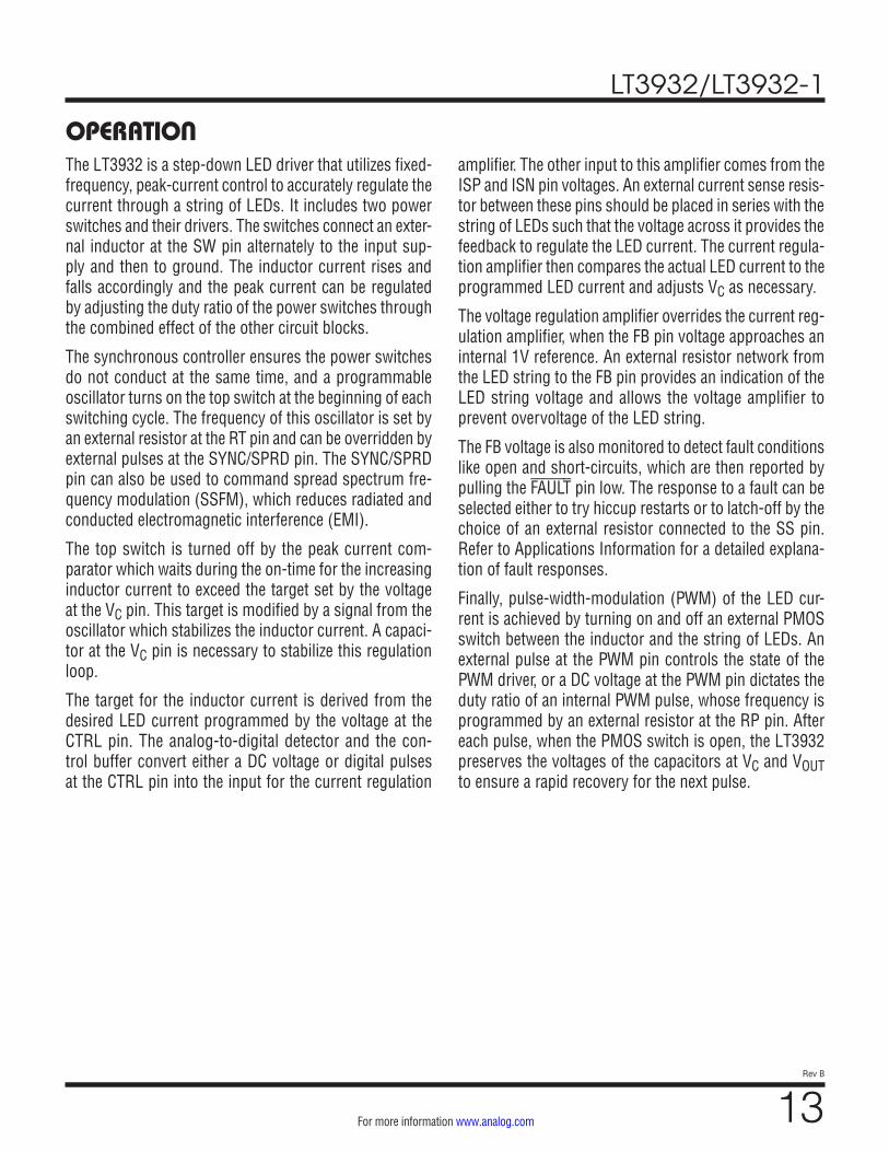
The choice of switching frequency should be made know-ing that, although the maximum LED current that can be programmed with the CTRL pin is 2A, the inductor current may exceed 2A when the frequency is high and the output voltage is low as in a short-circuit. This is because there is a minimum on-time for which the SW pin will be driven high during each switching period. The inductor current increases during this time, and if the frequency is high and the output voltage low, there may not be enough off-time remaining in each switching period for the inductor cur-rent to decrease back to the level at which it started. In this case, the net inductor current would increase with each switching period regardless of the state of the CTRL pin.
To prevent large inductor currents that would damage the LT3932, the high-side switch is not turned on until the inductor current decreases to less than the DA current limit, which is approximately 2.3A. While the high-side switch is off, the current is sensed through the low-side switch. The peak inductor current may increase to 3.6A, but the off-time and the switching period are extended until the inductor current reaches equilibrium as shown in Figure 5.
WITH SSFMWITHOUT SSFM
FREQUENCY (MHz)1 3 5 7 9 11
–40
–20
0
20
40
60
80
100
AMPL
ITUD
E (d
BuV)
3932 F04
LT3932/LT3932-1
16Rev B
For more information www.analog.com
APPLICATIONS INFORMATION
The DA current limit is relevant only when the output capacitor is shorted to GND. When instead the LED string is shorted to GND, the voltage across the external PMOS (described later) is high enough that the required on-time is greater than the minimum on-time. This means that, in spite of a shorted LED string, the inductor current remains in regulation even at the highest switching frequency.
Selecting an Inductor
The inductor must be rated for the current limit regardless of the intended application. Its value, in most applications, should be selected such that the inductor current ripple is not more than 25% of the maximum output current. When that current is 2A, for example, the minimum inductance can be calculated using the following equation:
L = 2µH •
VOUTVIN(MAX)
•VIN(MAX) – VOUT
1V•1MHzfSW
However, for high output voltages even the above equation would suggest an inductance value that is too small. For stability, the LT3932 requires an inductance greater than:
L = 1µH •
VOUT1V
•1MHzfSW
Choose the larger of the values given by these equations. The manufacturers featured in Table 2 are recommended sources of inductors.
Table 2. Inductor ManufacturersMANUFACTURER WEBSITE
Würth Elektronik www.we-online.com
Coilcraft www.coilcraft.com
Selecting an Output Capacitor
Some applications are sensitive to ripple current in the LED string. In those cases, a capacitor at the output will absorb part of the inductor current ripple and thereby reduce the LED current ripple. Typically, the value of this capacitance is inversely proportional to the switching fre-quency and the output voltage as shown below:
COUT = 100µF •
1VVOUT
•1MHzfSW
However, applications may still be stable with more or less capacitance, and more capacitance may improve LED current waveforms for large PWM dimming ratios.
Use X7R or X5R ceramic capacitors as they retain their capacitance better than other capacitor types over a wide voltage and temperature range. Sources of quality ceramic and electrolytic capacitors are listed in Table 3.
Table 3. Capacitor ManufacturersMANUFACTURER WEBSITE
Murata Manufacturing www.murata.com
Garrett Electronics www.garrettelec.com
AVX www.avx.com
Nippon Chemi-Con www.chemi-con.co.jp/e
Stabilizing the Regulation Loop
Stabilizing the regulation loop typically requires only a capacitor CC connected from the VC pin to GND. For most designs, values between 1nF and 10nF are suitable. When using an output capacitor COUT larger than 10µF, as is needed for large PWM dimming ratios, a resistor RC in series with CC may be necessary. Larger values of COUT require larger values of RC. See Typical Applications for some examples.
Selecting and Placing the Input Capacitors
Although they do not impact stability, several capacitors are necessary between VIN and GND to properly bypass the input supply voltage. At least 10μF is required in total, although it does not have to be composed entirely of ceramic capacitors placed very close to the VIN pins. However, it is important that a ceramic capacitor be placed
Figure 5. Extended Off-Time at Current Limit
OUTPUT SHORTED
DA CURRENT LIMIT
100µs/DIV
INDUCTORCURRENT
500mA/DIV
3932 F05

LT3932/LT3932-1
17Rev B
For more information www.analog.com
APPLICATIONS INFORMATION
Figure 6. Placement of Input Capacitors
as close as possible to each of the pairs of VIN pins (Pins 16 and 17 as well as 20 and 21) and their adjacent GND pins as shown in Figure 6. These two capacitors should be at least 1μF if possible. Because the SW pins lie between the VIN pins, it is convenient to join the VIN pins using a trace on the second layer of the circuit board.
Another 1μF capacitor should be placed very close to the remaining VIN pin (Pin 26), which supplies the internal control circuitry.
contrast to a low-side NMOS driver, this feature eliminates the need for a dedicated return path for the LED current in automotive applications or other grounded chassis systems.
The gate driver for this PMOS draws power through the VOUT pin, which must be connected even in applications that do not require PWM dimming. When the PWM pin voltage is greater than 1.4V, the driver will pull the gate of the PMOS to a maximum of 10V below the VOUT pin. If VOUT is below 10V, the gate drive is necessarily reduced. For constant current applications, leave PWMTG open, connect the load directly after the current sense resistor, and connect PWM to INTVCC. In these cases, analog dim-ming may be implemented with the CTRL pin.
The drain-source voltage rating of the chosen PMOS should be greater than the maximum output voltage. Typically the output voltage is a little higher than the sum of the forward voltages of the LEDs in the string. However, when the string is broken, the output voltage will begin to increase due to the imbalance of inductor current and load current. As described in detail later, the LT3932 will not reduce the inductor current nor limit the output volt-age until the FB pin voltage approaches 1V. Therefore, the maximum output voltage is ultimately determined by the resistor network between FB and VOUT.
In most applications, the gate-source voltage rating of the PMOS should be at least 10V. The only exceptions to this rule are applications for which the output voltage is always less than 10V. The PWMTG driver will try to pull the gate of the PMOS down to 10V below VOUT, but it cannot pull the gate below GND. Therefore, when the maximum output voltage is less than 10V, the PMOS gate source voltage rating will be sufficient if it is merely equal to or greater than the output voltage.
Finally, the drain current rating of the PMOS must exceed the programmed LED current. Assuming this condition and the conditions above are met, the only electrical parameter to be considered is the on-resistance. Other parameters such as gate charge are less important because PWM dimming frequencies are typically too low for efficiency to be affected noticeably by gate charging loss or transition loss.
15 16 17 18 19
8 7 6 5 4
20 21 22
3 2 1
14
13
12
11
10
9
23
24
25
26
27
28
29
GND1µF
100nF
GND
3932 F06
SW
VIN
VIN VINBST
1µFCERAMIC
GND
1µFCERAMICGND
TOP LAYER BOTTOM LAYER
Selecting a MOSFET for PWM Dimming
Pulse-Width-Modulation (PWM) dimming of the LED cur-rent is an effective way to control the brightness of the light without varying its color. The brightness can also be adjusted more accurately this way than by varying the current level.
The LT3932 features a PWMTG driver that is intended for a high-voltage PMOS switch in position to effectively PWM dim a string of LEDs from the output capacitor and current sense resistor. When the switch is open and the string is disconnected, the LED current will be zero. In

LT3932/LT3932-1
18Rev B
For more information www.analog.com
APPLICATIONS INFORMATIONTable 4 lists recommended manufacturers of PMOS devices.
Table 4. PMOS ManufacturersMANUFACTURER WEBSITE
Infineon www.infineon.com
Vishay Intertechnology www.vishay.com
NXP Semiconductors www.nxp.com
Selecting an RP Resistor for Internal PWM Dimming
If the RP pin is tied to GND, an external pulse-width mod-ulated signal at the PWM pin will control PWM dimming of the LED load. The signal will enable the PWMTG driver and turn on the external PMOS device when it is higher than 1.4V.
However, the LT3932 is capable of PWM dimming even when an external PWM signal is not available. In this case, an internal PWM signal with frequency set by a resistor at the RP pin and duty ratio set by a DC voltage at the PWM pin will control the PWMTG driver. The RP resistor should be one of the seven values listed in Table 5. For each of these values, the PWM frequency is a unique ratio of the switching frequency.
Table 5. Internal PWM Dimming Frequencies
RP
SWITCHING FREQUENCY2MHz 1MHz 500KHz 250KHz
28.7k 7.81kHz 3.91kHz 1.95kHz 977Hz47.5k 3.91kHz 1.95kHz 977Hz 488Hz76.8k 1.95kHz 977Hz 488Hz 244Hz118k 977Hz 488Hz 244Hz 122Hz169k 488Hz 244Hz 122Hz 61Hz237k 244Hz 122Hz 61Hz 31Hz332k 122Hz 61Hz 31Hz 15Hz
When using the internal PWM signal, set the voltage at the PWM pin between 1V and 2V. The PWMTG driver will stay off if PWM is below 1V, and it will stay on if PWM is above 2V. Between 1V and 2V there are 128 evenly spaced thresholds corresponding to 128 discrete PWM duty ratios from 0% to 100%. This range of 1V to 2V has been chosen so that the PWM voltage may be set using a potentiometer or a resistor network and the 2V refer-ence available at the VREF pin. Place a small 1µF ceramic capacitor near the PWM pin to ground.
Figure 7. ISMON Filter Configuration
There are a couple of exceptions to the PWM dimming behavior described above. First, once initiated, the PWM on-time will will last at least four switching cycles regard-less of the signal at the PWM pin and the resistor at the RP pin. This ensures that the current regulation loop has enough time to reach equilibrium but still allows for a 5000:1 dimming ratio when the PWM frequency is 100Hz and the switching frequency is 2MHz. The LT3932-1 does not enforce this four-cycle limit so that dimming ratios of 10000:1 or greater are possible in some applications. Second, to avoid excessive start-up times, after the first PWM pulse, PWMTG will stay on until the SS pin voltage reaches 1.7V or the LED current has reached 10% of the full-scale current.
PWM Dimming with Very Long Off Times
To enhance PWM dimming, the VOUT and VC pin voltages are driven when the PWM pulse (internal or external) is at a logic low to maintain the charge on the capacitors at those pins. Consequently, when PWM returns to a logic high state, the LED current can quickly reach the regulated level even if PWM was low for a very long time. This fea-ture facilitates machine vision applications which require a synchronized strobe light or brief illuminating flashes on short delay.
Monitoring LED Current
The ISMON pin provides an amplified and buffered mon-itor of the voltage between the ISP and ISN pins. The gain of the internal amplifier is ten, and the speed is fast enough to track the pulse-width modulated LED current. However, as shown in Figure 7, the ISMON voltage can be filtered with a resistor-capacitor network to monitor the average LED current instead.
LT3932
3932 F07
ISMONRMON
CMON
LT3932/LT3932-1
19Rev B
For more information www.analog.com
APPLICATIONS INFORMATION
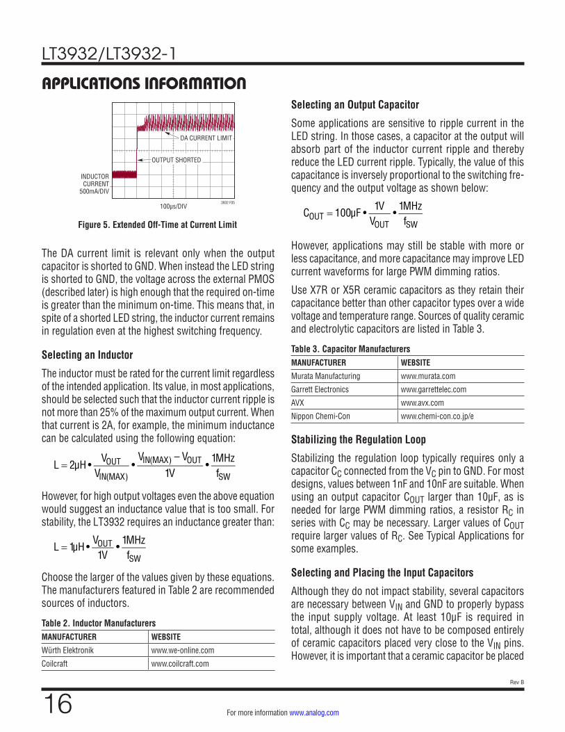
Figure 8. FB Resistor Configuration
Figure 9. FAULT Resistor Configuration
The resistor should be 1MΩ. The capacitance can be as large or small as needed without affecting the stability of the internal amplifier. For example, when the PWM fre-quency is 200Hz, a 100nF capacitor combined with the 1MΩ resistor would limit the ripple on ISMON to 1%.
LT3932
3932 F08
FB
VOUT
RFB2
RFB1 VOUT(MAX) = 1V • 1+
RFB2RFB1
LT3932
3932 F09
FAULT
INTVCC
RFAULT
Understanding FB Overvoltage Lockout
It is possible that the FB voltage can exceed the 1V limit. If the output voltage is near the maximum when the LED string opens, it may take too long for the feedback loop to adjust the inductor current and avoid overcharging the output. However, if the FB voltage exceeds the 1.05V Overvoltage Lockout Threshold, the LT3932 will immedi-ately stop switching and resume only when FB decreases to 1V.
This threshold may be routinely exceeded when the LT3932 is being operated as a voltage regulator and the load current decreases rapidly. In this case, the pause in switching limits the output overshoot and ensures that the voltage is back in regulation as quickly as possible. For safe operation, choose RFB2 and RFB1 values to ensure the output voltage is not greater than VIN when the FB voltage is 1.05V.
Open and Shorted LED Fault Detection and Response
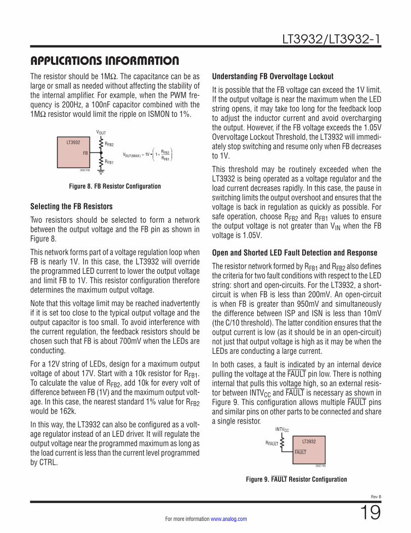
The resistor network formed by RFB1 and RFB2 also defines the criteria for two fault conditions with respect to the LED string: short and open-circuits. For the LT3932, a short-circuit is when FB is less than 200mV. An open-circuit is when FB is greater than 950mV and simultaneously the difference between ISP and ISN is less than 10mV (the C/10 threshold). The latter condition ensures that the output current is low (as it should be in an open-circuit) not just that output voltage is high as it may be when the LEDs are conducting a large current.
In both cases, a fault is indicated by an internal device pulling the voltage at the FAULT pin low. There is nothing internal that pulls this voltage high, so an external resis-tor between INTVCC and FAULT is necessary as shown in Figure 9. This configuration allows multiple FAULT pins and similar pins on other parts to be connected and share a single resistor.
Selecting the FB Resistors
Two resistors should be selected to form a network between the output voltage and the FB pin as shown in Figure 8.
This network forms part of a voltage regulation loop when FB is nearly 1V. In this case, the LT3932 will override the programmed LED current to lower the output voltage and limit FB to 1V. This resistor configuration therefore determines the maximum output voltage.
Note that this voltage limit may be reached inadvertently if it is set too close to the typical output voltage and the output capacitor is too small. To avoid interference with the current regulation, the feedback resistors should be chosen such that FB is about 700mV when the LEDs are conducting.
For a 12V string of LEDs, design for a maximum output voltage of about 17V. Start with a 10k resistor for RFB1. To calculate the value of RFB2, add 10k for every volt of difference between FB (1V) and the maximum output volt-age. In this case, the nearest standard 1% value for RFB2 would be 162k.
In this way, the LT3932 can also be configured as a volt-age regulator instead of an LED driver. It will regulate the output voltage near the programmed maximum as long as the load current is less than the current level programmed by CTRL.

LT3932/LT3932-1
20Rev B
For more information www.analog.com
APPLICATIONS INFORMATIONSoft-Start and Fault Modes
The SS pin has two functions. First, it allows the user to program the output voltage startup ramp rate. An internal 20μA current pulls up the SS pin to INTVCC. Connecting an external capacitor CSS from the SS pin to GND, as shown in Figure 10, will generate a linear ramp voltage. The LT3932 regulates the FB pin voltage to track the SS pin voltage until VOUT is high enough to drive the LED at the commanded current level.
part of the cycle before being interrupted. Although the LT3932 can safely endure a short-circuit while continu-ously switching, this hiccup action saves power. The fre-quency of the hiccups is inversely proportional to CSS and 100nF yields about 8Hz.
The operating point of a voltage regulator supplying light loads will frequently satisfy the criteria for an open-circuit, and the hiccup behavior would therefore be very disrup-tive. So when the LT3932 is configured as a voltage regu-lator, a resistor RSS should be connected between INTVCC and SS as shown in Figure 10.
The current that pulls down the SS pin during a fault is so weak that if RSS is 1MΩ, the voltage at the SS pin will never reach 1.7V. Therefore, the LT3932 will not stop switching or start to hiccup. With this resistor, the LT3932 will continue switching and rely on overvoltage and over-current protection to guarantee safe operation in the event of open-circuits and short-circuits.
If the resistor is changed to 2MΩ, then the SS pin may be discharged to less than 1.7V, but not less than 200mV as shown in Figure 12. The LT3932 will consequently cease switching permanently until being reset by the EN/UVLO pin or by powering off. Some applications may demand this behavior so that short and open-circuits can be inves-tigated manually before resuming normal operation.
This latch-off behavior is the third of three ways that the LT3932 can be programmed to respond to faults—the other two being continuous operation and the default hic-cup behavior.
Figure 12. Latch-Off Response to a Fault
The SS pin is also used as a fault timer. After a fault is detected, an internal 1.25μA current sink will begin to discharge the soft-start capacitor and lower the voltage at the SS pin. When the voltage falls from 3.3V to 1.7V, all switching will cease, but the SS pin will continue to discharge. Switching will not resume until SS reaches 200mV. At this point, the 20μA current will recharge the soft-start capacitor, and the LT3932 will try to switch again. If the fault persists when SS returns to 1.7V, the process will repeat as shown in Figure 11.
The charging rate of the soft-start capacitor is much faster than the discharging rate, so while the fault persists, the LT3932 will only attempt switching for a relatively short
Figure 11. Hiccup Response to Fault
Figure 10. SS Capacitor and Resistor Configuration
LT3932
3932 F10
SS
INTVCC
RSS
CSS
FAULT DETECTED
FAULT CLEARED
10ms/DIV
SS1V/DIV
3932 F11
FAULT DETECTEDCONTINUOUS
RSS = 1MEG
LATCH–OFFRSS = 2MEG
10ms/DIV
SS1V/DIV
3932 F12

LT3932/LT3932-1
21Rev B
For more information www.analog.com
APPLICATIONS INFORMATION
Figure 13. EN/UVLO Resistor Configuration
Dimming with External Drivers
Continuous operation in response to a fault also enables the LT3932 to operate with external switches that shunt some or all of the LEDs in the string. The LT3965 8-switch Matrix LED Dimmer, for example, is designed to shunt a changing combination of up to eight LEDs in a single string with independent PWM dimming signals. See Typical Applications for more details.
Programming the EN/UVLO Threshold
An external voltage source can be used to set the voltage at the EN/UVLO pin to enable or disable the LT3932. The LT3932 will stop switching, disable the PWMTG driver, and reset the SS pin when the voltage at EN/UVLO drops below 1.15V, but internal circuitry will continue drawing current. Full shutdown is guaranteed when EN/UVLO is below 300mV, and in full shutdown the LT3932 will draw less than 2μA. For applications in which the level of the source driving EN/UVLO changes slowly, 20mV of hys-teresis has been added to the 1.15V enable threshold.
Alternatively, a resistor network can be placed between VIN and EN/UVLO as shown in Figure 13. In this case, EN/UVLO automatically falls below 1.15V and disables
switching when VIN falls below a certain level, called the Undervoltage Lockout (UVLO) threshold, which is defined by resistors REN1 and REN2. Additionally, a 4μA current is designed to flow into EN/UVLO when the pin voltage is below the threshold. This current provides additional hysteresis. To define the hysteresis (VHYST) and the UVLO threshold (VUVLO) select REN1 and REN2 according to the following equations:
REN2 =
VHYST4µA
–VUVLO480µA
REN1 =
1.15 •REN2VUVLO – 1.15
For example, to program a 10V threshold with 1V of hysteresis, use 226k and 29.4k for REN2 and REN1, respectively.
Planning for Thermal Shutdown
The LT3932 automatically stops switching when the internal temperature is too high. The temperature limit is guaranteed to be higher than the operational temperature of the part. During thermal shutdown, all switching is ter-minated, SS is forced low, and the LEDs are disconnected using the PWMTG driver.
The exposed pad on the bottom of the package must be soldered to a ground plane. Vias placed directly under the package are necessary to dissipate heat. Following these guidelines, the official four-layer demo board DC2286A reduces thermal resistance θJA to 25°C/W, but with a com-promised board design θJA could be 40°C/W or higher.
LT3932
3932 F13
EN/UVLO
VIN
REN2
REN1

LT3932/LT3932-1
22Rev B
For more information www.analog.com
APPLICATIONS INFORMATIONDesigning the Printed Circuit Board
Note that large switched currents flow through the local input capacitors and the VIN and GND pins. The loops traveled by these currents should be made as small as possible by keeping the capacitors as close as possible to these pins. These capacitors, as well as the inductor, should be placed on the same side of the board as the LT3932 and connected on the same layer. Other large, bulk input capacitors can be safely placed farther from the chip and on the other side of the board.
Create a Kelvin ground network by keeping the ground connection for all of the other components separate. It should only join the ground for the input and output capacitors and the return path for the LED current at the exposed pad.
There are a few other aspects of the board design that improve performance. An unbroken ground plane on the second layer dissipates heat, but also reduces noise. Likewise minimizing the area of the SW and BST nodes reduces noise. The traces for FB and VC should be kept short to lessen the susceptibility to noise of these high impedance nodes. Matched kelvin connections from the external current sense resistor RS to the ISP and ISN pins are essential for current regulation accuracy. The 2.2μF INTVCC and VREF capacitors as well as the 22nF BST capacitor should be placed as closely as possible to their respective pins. A capacitor for the CTRL pin and, when the internal dimming feature is used, the PWM pin, can compensate for compromised layouts. Finally, a diode with anode connected to ground and cathode to the drain of the PWMTG MOSFET can protect that device from over-voltage caused by excessive inductance in the LED string. Please refer to the demo board layout of the LT3932 for an example of how to implement these recommendations.
LT3932/LT3932-1
23Rev B
For more information www.analog.com
TYPICAL APPLICATIONS2A LED Driver with Duty Cycle LED Current
RT523k
287kRFB2
10kRFB1
RS50mΩ
M1
LED1
22nFCBST
2×10µFCOUT
CREF2.2µF
CVCC2.2µF
CSS100nF
CC10nF
CIN22×1µF
L1150µH
LED8
RFAULT100k
CIN110µF
VIN
EN/UVLO
VREF
CTRL
PWM
SYNC/SPRD
INTVCC
SS RT RP VC
ISP
GND
ISN
FB
VOUT
SW
BST
D1INTVCC
LT3932
PWMTG
VIN36V
200kHz
L1: WURTH 7447709151
D1: NEXPERIA BAT46WJ
M1: VISHAY Si4447ADYRS: OHMITE LVK12R050DCOUT1: MURATA GRM32ER71H106K
ISMON
FAULTFAULT
ISMON
3.3V0V
3.3V0V
ENABLE
3932 TA02
2A MAX
Digital CTRL 25%, Digital PWM 100%
Digital CTRL 50%, Digital PWM 100%
Digital CTRL 25%, Digital PWM 25%
Digital CTRL 25%, Digital PWM 50%
500ns/DIV
CTRL5V/DIV
PWM2V/DIV
LED CURRENT1A/DIV
3932 TA02a500ns/DIV
CTRL5V/DIV
PWM2V/DIV
LED CURRENT1A/DIV
3932 TA02b
5ms/DIV
CTRL5V/DIV
PWM5V/DIV
LED CURRENT500mA/DIV
3932 G335ms/DIV
CTRL5V/DIV
PWM5V/DIV
LED CURRENT500mA/DIV
3932 TA02d

LT3932/LT3932-1
24Rev B
For more information www.analog.com
TYPICAL APPLICATIONS24V Voltage Regulator with Spread Spectrum
VINVIN
29V TO 36V CIN110µF
EN/UVLO
L1: COILCRAFT XAL5050-153RS: OHMITE LVK12R050DCOUT: GRM32ER71H106KD1: NEXPERIA BAT46WJ
INTVCC
FAULT
BST
D1
INTVCC
SW
VOUT
FB
RP VCRT
ISP
GND
ISN
ISMON
3932 TA03
LT3932
RFB1226k
RFB210k
RS50mΩ
RFAULT100k
RC20k
CIN22×1µF
CC10nF
CBST22nF
L115µH
COUT2 × 10µF
VOUT24V, 2A MAX
REN2576k
REN123.7k
SS
RT45.3k2MHz
CSS10nF
RSS1MEGΩ
CVCC2.2µF
VREF
CTRL
PWM
SYNC/SPRD
CREF2.2µF
PWMTG NOT USED
Efficiency Load Step Response (100mA to 1A)
EFFICIENCY (29VIN)LOSS (29VIN)EFFICIENCY (36VIN)LOSS (36VIN)
OUTPUT CURRENT (mA)0 500 1000 1500 2000
92
93
94
95
96
97
0.5
1.0
1.5
2.0
2.5
3.0
EFFI
CIEN
CY (%
)
ON–CHIP LOSS (W)
3932 TA03a
100µs/DIV
VOUT1V/DIV
ILOAD500mA/DIV
3932 TA03b

LT3932/LT3932-1
25Rev B
For more information www.analog.com
TYPICAL APPLICATIONS
REN1
CIN41µF
REN2
RT45.3k
RC24.9k
RFB269.8k
RFB110k
RS100mΩ
M1
LED1
LED2
CBST22nF
CIN24.7µF
COUT4.7µFCREF
2.2µF
CVCC10µF
CSS1nF
CC150pF
CB2100nF
CIN52x470nF
L12.2µH
D1
3932 TA07
CIN333µF
VIN
EN/UVLO
VREF
CTRLPWM
SYNC/SPRD
INTVCC
SS RT RP VC
ISP
ISN
FB
VOUT
SW
BST
D1
INTVCC
LT3932
ISMON, FAULT NOT USED
PWMTG
VIN8V TO 36V
2MHz
D1: NXP PMEG4010CEJ
D1: NEXPERIA BAT46WJ
RS: SUSUMU KRL1220D-M-R100-F
FB1,2: WURTH 742792040L1: WURTH 74438323022M1: VISHAY Si2399DS
50V1206
50VELYT.
50V0603
50V0402
16V0805
16V0402
GND
FB2
FB1
232k
39.2k
CIN12x100nF50V0402
1A MAX
DC2286A DEMO BOARD14V INPUT TO 6V OUTPUT AT 1A
CLASS 5 PEAK LIMITMEASURED EMISSIONSAMBIENT NOISE
FREQUENCY (MHz)0.1 1 10 100 200
–20
–10
0
10
20
30
40
50
60
70
80
AMPL
ITUD
E (d
BµV)
3932 TA07a DC2286A DEMO BOARD14V INPUT TO 6V OUTPUT AT 1A
CLASS 5 PEAK LIMITMEASURED EMISSIONSAMBIENT NOISE
FREQUENCY (MHz)0 100 200 300 400 500 600 700 800 900 1000
–20
–10
0
10
20
30
40
50
60
70
80
AMPL
ITUD
E (d
BµV/
m)
3932 TA07b
DC2286A DEMO BOARD14V INPUT TO 6V OUTPUT AT 1A
CLASS 5 AVERAGE LIMITMEASURED EMISSIONSAMBIENT NOISE
FREQUENCY (MHz)0.1 1 10 100 200
–20
–10
0
10
20
30
40
50
60
70
80
AMPL
ITUD
E (d
BµV)
3932 TA07c DC2286A DEMO BOARD14V INPUT TO 6V OUTPUT AT 1A
CLASS 5 AVERAGE LIMITMEASURED EMISSIONSAMBIENT NOISE
FREQUENCY (MHz)0 100 200 300 400 500 600 700 800 900 1000
–20
–10
0
10
20
30
40
50
60
70
80
AMPL
ITUD
E (d
BµV/
m)
3932 TA07d
CISPR25 Peak Conducted Emissions Test
CISPR25 Average Conducted Emissions Test
CISPR25 Peak Radiated Emissions Test
CISPR25 Average Radiated Emissions Test

LT3932/LT3932-1
26Rev B
For more information www.analog.com
TYPICAL APPLICATIONS2A LED Driver with Internal PWM Dimming
Internal PWM Dimming Internal PWM Dimming
REN129.4k
REN2274k
RT45.3k
110kRFB2
10kRFB1
RS50mΩ
M1
LED1
LED2
22nFCBST
CREF2.2µF
CVCC2.2µF
CSS100nF
CC10nF
CIN22×1µF
L18.2µH
RP28.7k
RC162k LED3
3932 TA06
RFAULT100k
RREF2100k
RREF1100k
CIN110µF
COUT100µF
VIN
EN/UVLO
VREF
CTRL
PWM
SYNC/SPRD
INTVCC
SS RT RP VC
ISP
ISN
FB
VOUT
SW
BST
D1INTVCC
LT3932
PWMTG
VIN12V TO 24V
2MHz
L1: WURTH 74404064082M1: INFINEON IRF7204
D1: NEXPERIA BAT46WJ
RS: OHMITE LVK12R050DCOUT: AVX TPME107M020R0035
ISMONFAULTFAULT ISMON
7.8kHz
GND2A MAX
PWM = 1.078V 2µs/DIV
SW20V/DIV
PWMTG10V/DIV
IL1A/DIV
ILED1A/DIV
3932 TA06aPWM = 1.132V 2µs/DIV
SW20V/DIV
PWMTG10V/DIV
IL1A/DIV
ILED1A/DIV
3932 TA06b

LT3932/LT3932-1
27Rev B
For more information www.analog.com
TYPICAL APPLICATIONS
Multiple String Drivers from Single Boosted 36V Input
VINCIN110µF
EN/UVLOENABLE1
VREF
PWM3.3V0V
CTRL
L1: WURTH 74437336100M1: INFINEON IRF7204RS1: OHMITE LVK12R050DCOUT: MURATA GRM32ER714475KD1: NEXPERIA BAT46WJ
L0: WÜRTH 7443630420M0: INFINEON BSZ040N04LSR0: VISHAY WSLP25124L000FD0: ONSEMI MBR1240MFS
INTVCC
FAULT
BST
D1INTVCC
SW
VOUT
FB
RP VCRT
ISP
GND
ISN
PWMTG
ISMON
LT3932RFB1110k
RFB210k
RFAULT100k
CIN22×1µF
CIN110µF
CIN22×1µF
CC10nF
CREF2.2µF
CBST22nF
L110µH
COUT4.7µF
M1
RS150mΩ
SS
RT45.3k2MHz
CSS100nF
CVCC2.2µF
SYNC/SPRD0V3.3V
RCTRL249.9k
RCTRL130.1k
VIN
+2 LT3932 (1A EACH)
EN/UVLOENABLE2
VREF
PWM0V3.3V
CTRL
L2: COILCRAFT LPS8045B-153M2: VISHAY Si2319CDSRS2: OHMITE LVK12R100DCOUT: MURATA GRM32ER71H475KD2: NEXPERIA BAT46WJ
INTVCC
FAULT
BST
SW
VOUT
FB
RP VCRT
ISP
GND
ISN
PWMTG
ISMON
3932 TA05
LT3932RFB1287k
RFB210k
RFAULT100k
CC10nF
CREF2.2µF
CBST22nF
L215µH
COUT4.7µF
M2
RS2100mΩ
SS
RT45.3k2MHz
CSS100nF
CVCC2.2µF
SYNC/SPRD0V3.3V
GATEVIN
SENSE
GND
SS
SHDN/UVLO
SYNC
VC
RT
LT3757
RSHDN248.7k
RSHDN112.1k
RC10k
RT30.9k400MHz
CC10nF
CSS100nF
L04.2µHD0
CIN10µF
VIN6V MIN FOR OPERATION10V MIN FOR FULL CURRENT
VBUCK36V, 5A MAX
R04mΩ
M0
RFB1348k
RFB216.2k
INTVCC
CVCC4.7µF
COUT5µF
COUT35µF50V
FBX
8×LED
+
D2INTVCC
1A MAX1A MAX

LT3932/LT3932-1
28Rev B
For more information www.analog.com
PACKAGE DESCRIPTION
4.00 ±0.10(2 SIDES)
2.50 REF
5.00 ±0.10(2 SIDES)
NOTE:1. DRAWING PROPOSED TO BE MADE A JEDEC PACKAGE OUTLINE MO-220 VARIATION (WGHD-3).2. DRAWING NOT TO SCALE3. ALL DIMENSIONS ARE IN MILLIMETERS4. DIMENSIONS OF EXPOSED PAD ON BOTTOM OF PACKAGE DO NOT INCLUDE MOLD FLASH. MOLD FLASH, IF PRESENT, SHALL NOT EXCEED 0.15mm ON ANY SIDE5. EXPOSED PAD SHALL BE SOLDER PLATED6. SHADED AREA IS ONLY A REFERENCE FOR PIN 1 LOCATION ON THE TOP AND BOTTOM OF PACKAGE
PIN 1TOP MARK(NOTE 6)
0.40 ±0.10
27 28
1
2
BOTTOM VIEW—EXPOSED PAD
3.50 REF
0.75 ±0.05 R = 0.115TYP
R = 0.05TYP
PIN 1 NOTCHR = 0.20 OR 0.35× 45° CHAMFER
0.25 ±0.05
0.50 BSC
0.200 REF
0.00 – 0.05
(UFD28) QFN 0816 REV C
RECOMMENDED SOLDER PAD PITCH AND DIMENSIONSAPPLY SOLDER MASK TO AREAS THAT ARE NOT SOLDERED
0.70 ±0.05
0.25 ±0.050.50 BSC
2.50 REF
3.50 REF4.10 ±0.055.50 ±0.05
2.65 ±0.05
3.10 ±0.054.50 ±0.05
PACKAGE OUTLINE
2.65 ±0.10
3.65 ±0.10
3.65 ±0.05
UFD Package28-Lead Plastic QFN (4mm × 5mm)
(Reference LTC DWG # 05-08-1712 Rev C)
LT3932/LT3932-1
29Rev B
For more information www.analog.com
Information furnished by Analog Devices is believed to be accurate and reliable. However, no responsibility is assumed by Analog Devices for its use, nor for any infringements of patents or other rights of third parties that may result from its use. Specifications subject to change without notice. No license is granted by implication or otherwise under any patent or patent rights of Analog Devices.
REVISION HISTORYREV DATE DESCRIPTION PAGE NUMBER
A 02/18 Added LT3932-1 to data sheet.Added 10000:1 PWM dimming ratio for LT3932-1 with supporting text in Features and Description.Added machine vision systems to Applications.Relabeled Soft-Start pin from S to SS.On Figure, added Schottky Diode from INTVCC to BST pin, changed boost capacitor from 100nF to 22nF.
Changed θJA from 43°C/W to 25°C/W (based on demo board measurement).Sense voltage VCTRL changed from 2V to 1.5V. ISN pin current VISN value changed from 24V to 23.9V.LED Current and LED Voltage Limit Graphs y-axis corrected to mV units.DA Limit graph retitled to “DA Current Limit”, input step changed from 20V upper limit to 25V on Input Voltage Transient Response graph.Added additional BST pin description text; corrected BST capacitor value from 100nF to 22nF. DA Current Limit added to Block Diagram.Text added to describe DA Current Limit.Added LT3932-1 text regarding four-cycle limit and machine vision usage.Added text regarding θJA equals 25°C/W using DC2286 demo board, corrected boost capacitor value.Corrected Typical Application figure, reduced VOUT from 30V to 24V, changed digital CTRL 50% graph y-axis from 5A/DIV to 5V/DIV.Add new Efficiency graph.Added Diode D1: Nexperia BAT46WJ.
111
1, 22, 24, 25, 281, 12, 22, 23, 24,
25, 26, 282379
111215182122
2322, 24, 25, 26, 28
B 07/18 Three revised UVLO graphs in Typical Performance Characteristics EN/UVLO description; Changed text from “A resistor network between this pin and GND” to “. . . this pin and VIN.” VREF description; Changed buffered reference drive current from 2mA to 1mA Corrected RSS from 1mΩ to 1MΩ Changed Inductor L1 value from 7438323022 to 74438323022 Increased Inductor value from 8.2µH to 10µH Changed Inductor; New Product Number; Changed L1 From 7440463082 to 74437336100
5 10 10 24 25 27 27

LT3932/LT3932-1
30Rev B
For more information www.analog.com
D16990-0-7/18(B)
ANALOG DEVICES, INC. 2018www.analog.com
RELATED PARTS
TYPICAL APPLICATION
PART NUMBER DESCRIPTION COMMENTS
LT3922 40V, 2A, 2MHz, Synchronous Boost LED Driver VIN: 2.7V to 40V, VOUT(MAX) = 40V, 5000:1 True Color PWM™ Dimming, 5mm × 5mm QFN and TSSOP-28E
LT3965 8-Switch Matrix LED Dimmer VIN: 8V to 60V, Digital Programmable 256:1 PWM Dimming, I2C Multidrop Serial Interface TSSOP-28E Package
LT3956 80V, 3.3A 1MHz, Step-Up/Down LED Driver VIN: 4.5V to 80V, VOUT(MAX) = 80V, 3000:1 True Color PWM Dimming, 5mm × 6mm QFN
LT3474 36V, 1A, 2MHz, Step-Down LED Driver VIN: 4V to 36V, VOUT(MAX) = 13.5V, 400:1 True Color PWM Dimming, TSSOP-16E
LT3475 Dual 36V, 1.5A, 2MHz, Step-Down LED Driver VIN: 4V to 36V, VOUT(MAX) = 13.5V, 3000:1 True Color PWM Dimming, TSSOP-20E
LT3476 Quad 36V, 1.5A, 2MHz, Step-Up/Down LED Driver VIN: 2.8V to 16V, VOUT(MAX) = 36V, 1000:1 True Color PWM Dimming, 5mm × 7mm QFN
LT3477 42V, 3A, 3.5MHz, Step-Up/Down LED Driver VIN: 2.5V to 25V, VOUT(MAX) = 40V, 4mm × 4mm QFN and TSSOP-20E
LT3478 42V, 4.5A, 2.5MHz, Step-Up/Down LED Driver VIN: 2.5V to 26V, VOUT(MAX) = 42V, 3000:1 True Color PWM Dimming, TSSOP-16E
LTM8040 36V, 1A, μModule, Step-Down LED Driver VIN: 4V to 36V, VOUT(MAX) = 13V, 250:1 True Color PWM Dimming, 9mm × 15mm × 4.32mm LGA
LTM8042 36V, 1A, μModule, Step-Up/Down LED Driver VIN: 3V to 30V, VOUT(MAX) = 36V, 3000:1 True Color PWM Dimming, 9mm × 15mm × 2.82mm LGA
LT3757 40V, 1MHz, Step-Up Controller VIN: 2.9V to 40V, Positive and Negative Output Voltages, 3mm × 3mm DFN and MSOP-10E
700mA Matrix LED Driver with Individual Dimming for 6 LEDs
REN110.2k
REN2249k
RT287k
267kRFB2
10kRFB1
RS100mΩ
LED6
LED2
22nFCBST
CREF2.2µF
CVCC2.2µF
CSS10nF
CC330pF
CIN22x1µF
L133µH
LED1
RSS1M
RREF2110k
CIN110µF
COUT22nF
REN4249k
REN310.7k
CVDD2.2µF
RSDA10k
RSCL10k
RALERT10k
RDD100k
RREF1105k
RPWM10k
D7
D1
D2
D6
VIN
EN/UVLO
VREF
CTRL
PWM
SYNC/SPRDINTVCC
SS RT RP VC
ISP
ISN
FB
VOUT
SW
BST
D1INTVCC
LT3932
VIN32V
350kHz
L1: WURTH 74437349330
D1: NEXPERIA BAT46WJ
D1-7: NXP PMEG4010CEJRS: OHMITE LVK12R100DER
GND
D6
D2
D1
S6
S2
S1
VIN
GND
EN/UVLO
SDA
SCL
ALERT
ADDR1-4 LEDREF
PWMCLK
VDD
LT3965
D7
D8
VDD
3.3V0V
350kHz
3932 TA04
S8
S7
50V 50V0402
START
PWMTG, FAULT, AND ISMON NOT USED
700mA
Related Documents


![3 Two Ways to Measure Temperature Feature Simplicity ...€¦ · editor@analog.com or to Dan Sheingold, Editor [dan.sheingold@analog.com] or Scott Wayne, Publisher and Managing ...](https://static.cupdf.com/doc/110x72/5e9fb3e69cfe7d3b494cce9e/3-two-ways-to-measure-temperature-feature-simplicity-editor-or-to-dan-sheingold.jpg)