LT3758/LT3758A 1 Rev G For more information www.analog.com APPLICATIONS n Automotive n Telecom n Industrial n Wide Input Voltage Range: 5.5V to 100V n Positive or Negative Output Voltage Programming with a Single Feedback Pin n Current Mode Control Provides Excellent Transient Response n Programmable Operating Frequency (100kHz to 1MHz) with One External Resistor n Synchronizable to an External Clock n Low Shutdown Current < 1µA n Internal 7.2V Low Dropout Voltage Regulator n Programmable Input Undervoltage Lockout with Hysteresis n Programmable Soft-Start n Small 10-Lead DFN (3mm × 3mm) and MSOPE Packages n AEC-Q100 Qualification Is in Progress TYPICAL APPLICATION DESCRIPTION High Input Voltage, Boost, Flyback, SEPIC and Inverting Controller The LT ® 3758/LT3758A are wide input range, current mode, DC/DC controllers which are capable of generating either positive or negative output voltages. They can be configured as either a boost, flyback, SEPIC or inverting converter. The LT3758/LT3758A drive a low side external N-channel power MOSFET from an internal regulated 7.2V supply. The fixed frequency, current-mode architecture results in stable operation over a wide range of supply and output voltages. The operating frequency of LT3758/LT3758A can be set with an external resistor over a 100kHz to 1MHz range, and can be synchronized to an external clock using the SYNC pin. A minimum operating supply voltage of 5.5V, and a low shutdown quiescent current of less than 1µA, make the LT3758/LT3758A ideally suited for battery- powered systems. The LT3758/LT3758A feature soft-start and frequency foldback functions to limit inductor current during start- up and output short-circuit. The LT3758A has improved load transient performance compared to the LT3758. 12V Output Nonisolated Flyback Power Supply FEATURES SENSE LT3758 V IN D SN V IN 36V TO 72V C IN 2.2μF 100V X7R 63.4k 200kHz GATE FBX GND INTV CC SHDN/UVLO SYNC RT SS 0.022μF 100V T1 1,2,3 (SERIES) 4,5,6 (PARALLEL) 1M 44.2k 0.47μF 100pF 10k 10nF 0.030Ω 15.8k 1% 105k 1% C VCC 4.7μF 10V X5R V OUT 12V 1.2A 3758 TA01 C OUT 47μF X5R 6.2k D1 SW M1 5.1Ω 1N4148 V C All registered trademarks and trademarks are the property of their respective owners. Document Feedback

Welcome message from author
This document is posted to help you gain knowledge. Please leave a comment to let me know what you think about it! Share it to your friends and learn new things together.
Transcript
LT3758/LT3758A
1Rev G
For more information www.analog.com
APPLICATIONS n Automotive n Telecom n Industrial
n Wide Input Voltage Range: 5.5V to 100V n Positive or Negative Output Voltage Programming
with a Single Feedback Pin n Current Mode Control Provides Excellent Transient
Response n Programmable Operating Frequency (100kHz to
1MHz) with One External Resistor n Synchronizable to an External Clock n Low Shutdown Current < 1µA n Internal 7.2V Low Dropout Voltage Regulator n Programmable Input Undervoltage Lockout with
Hysteresis n Programmable Soft-Start n Small 10-Lead DFN (3mm × 3mm) and
MSOPE Packages n AEC-Q100 Qualification Is in Progress
TYPICAL APPLICATION
DESCRIPTION
High Input Voltage, Boost, Flyback, SEPIC and
Inverting Controller
The LT®3758/LT3758A are wide input range, current mode, DC/DC controllers which are capable of generating either positive or negative output voltages. They can be configured as either a boost, flyback, SEPIC or inverting converter. The LT3758/LT3758A drive a low side external N-channel power MOSFET from an internal regulated 7.2V supply. The fixed frequency, current-mode architecture results in stable operation over a wide range of supply and output voltages.
The operating frequency of LT3758/LT3758A can be set with an external resistor over a 100kHz to 1MHz range, and can be synchronized to an external clock using the SYNC pin. A minimum operating supply voltage of 5.5V, and a low shutdown quiescent current of less than 1µA, make the LT3758/LT3758A ideally suited for battery-powered systems.
The LT3758/LT3758A feature soft-start and frequency foldback functions to limit inductor current during start-up and output short-circuit. The LT3758A has improved load transient performance compared to the LT3758.
12V Output Nonisolated Flyback Power Supply
FEATURES
SENSE
LT3758
VIN
DSN
VIN36V TO
72V CIN2.2µF100VX7R
63.4k200kHz
GATE
FBXGND INTVCC
SHDN/UVLO
SYNC
RTSS
0.022µF100V T1
1,2,3(SERIES)
4,5,6(PARALLEL)
1M
44.2k
0.47µF
100pF10k
10nF0.030Ω 15.8k
1%
105k1%
CVCC4.7µF10VX5R
VOUT12V1.2A
3758 TA01
COUT47µFX5R
6.2k
D1
SW
M1
5.1Ω1N4148VC
All registered trademarks and trademarks are the property of their respective owners.
Document Feedback
LT3758/LT3758A
2Rev G
For more information www.analog.com
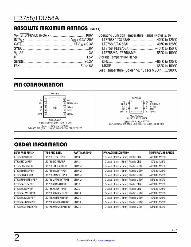
PIN CONFIGURATION
ABSOLUTE MAXIMUM RATINGSVIN, SHDN/UVLO (Note 7) ......................................100V INTVCC ....................................................VIN + 0.3V, 20VGATE ........................................................ INTVCC + 0.3VSYNC ..........................................................................8VVC, SS .........................................................................3VRT ............................................................................................... 1.5VSENSE ....................................................................±0.3VFBX ................................................................. –6V to 6V
(Note 1)
TOP VIEW
DD PACKAGE10-LEAD (3mm × 3mm) PLASTIC DFN
TJMAX = 125°C, θJA = 43°C/WEXPOSED PAD (PIN 11) IS GND, MUST BE SOLDERED TO PCB
10
9
6
7
8
4
5
11GND3
2
1 VIN
SHDN/UVLO
INTVCC
GATE
SENSE
VC
FBX
SS
RT
SYNC
12345
VCFBXSSRT
SYNC
109876
VINSHDN/UVLOINTVCCGATESENSE
TOP VIEW
MSE PACKAGE10-LEAD PLASTIC MSOP
TJMAX = 150°C, θJA = 40°C/WEXPOSED PAD (PIN 11) IS GND, MUST BE SOLDERED TO PCB
11GND
ORDER INFORMATIONLEAD FREE FINISH TAPE AND REEL PART MARKING* PACKAGE DESCRIPTION TEMPERATURE RANGE
LT3758EDD#PBF LT3758EDD#TRPBF LDNK 10-Lead (3mm × 3mm) Plastic DFN –40°C to 125°C
LT3758IDD#PBF LT3758IDD#TRPBF LDNK 10-Lead (3mm × 3mm) Plastic DFN –40°C to 125°C
LT3758EMSE#PBF LT3758EMSE#TRPBF LTDNM 10-Lead (3mm × 3mm) Plastic MSOP –40°C to 125°C
LT3758IMSE #PBF LT3758IMSE#TRPBF LTDNM 10-Lead (3mm × 3mm) Plastic MSOP –40°C to 125°C
LT3758HMSE#PBF LT3758HMSE#TRPBF LTDNM 10-Lead (3mm × 3mm) Plastic MSOP –40°C to 150°C
LT3758MPMSE #PBF LT3758MPMSE#TRPBF LTDNM 10-Lead (3mm × 3mm) Plastic MSOP –55°C to 150°C
LT3758AEDD#PBF LT3758AEDD#TRPBF LGGS 10-Lead (3mm × 3mm) Plastic DFN –40°C to 125°C
LT3758AIDD#PBF LT3758AIDD#TRPBF LGGS 10-Lead (3mm × 3mm) Plastic DFN –40°C to 125°C
LT3758AEMSE#PBF LT3758AEMSE#TRPBF LTGGK 10-Lead (3mm × 3mm) Plastic MSOP –40°C to 125°C
LT3758AIMSE#PBF LT3758AIMSE#TRPBF LTGGK 10-Lead (3mm × 3mm) Plastic MSOP –40°C to 125°C
LT3758AHMSE#PBF LT3758AHMSE#TRPBF LTGGK 10-Lead (3mm × 3mm) Plastic MSOP –40°C to 150°C
LT3758AMPMSE#PBF LT3758AMPMSE#TRPBF LTGGK 10-Lead (3mm × 3mm) Plastic MSOP –55°C to 150°C
Operating Junction Temperature Range (Notes 2, 8) LT3758E/LT3758AE ........................... –40°C to 125°C LT3758I/LT3758AI ............................. –40°C to 125°C LT3758H/LT3758AH .......................... –40°C to 150°C LT3758MP/LT3758AMP ..................... –55°C to 150°C
Storage Temperature Range DFN .................................................... –65°C to 125°C MSOP ................................................ –65°C to 150°C
Lead Temperature (Soldering, 10 sec) MSOP ........ 300°C
LT3758/LT3758A
3Rev G
For more information www.analog.com
ORDER INFORMATION
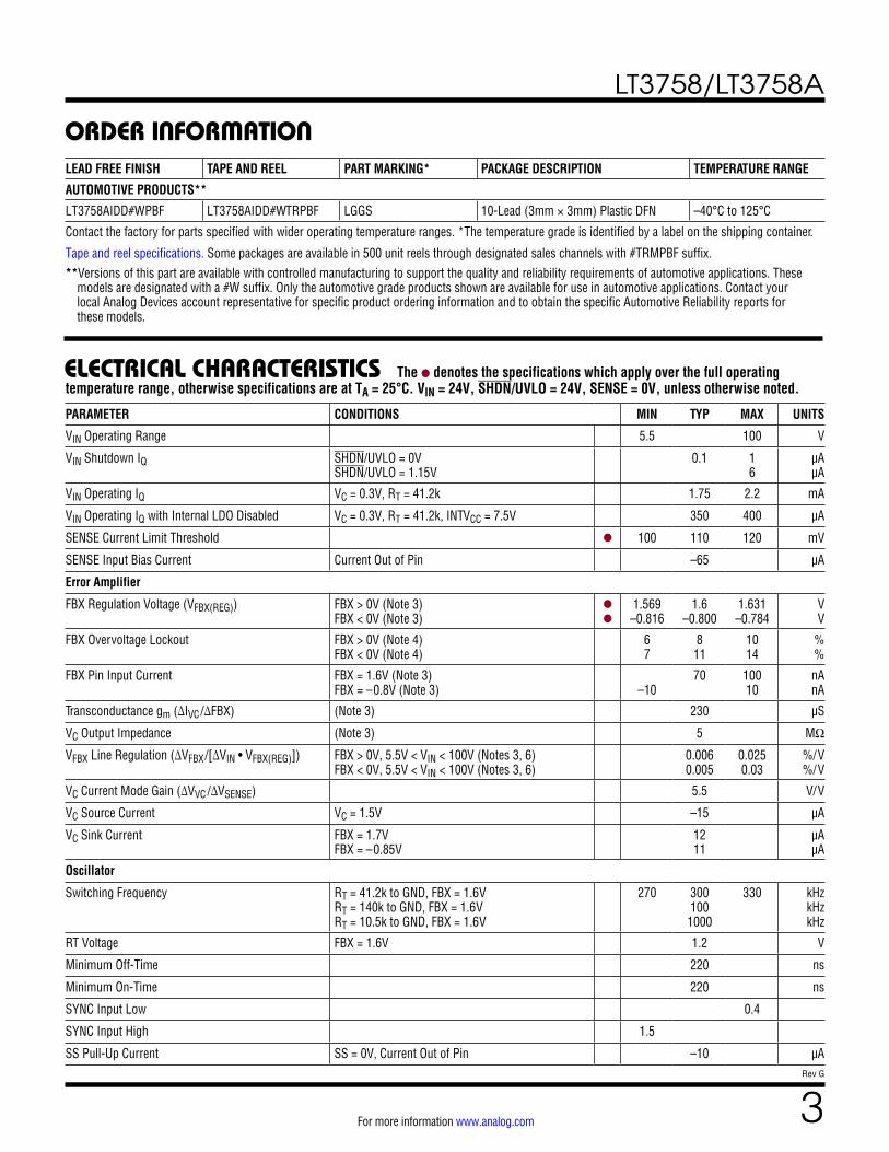
ELECTRICAL CHARACTERISTICS The l denotes the specifications which apply over the full operating temperature range, otherwise specifications are at TA = 25°C. VIN = 24V, SHDN/UVLO = 24V, SENSE = 0V, unless otherwise noted.
PARAMETER CONDITIONS MIN TYP MAX UNITS
VIN Operating Range 5.5 100 V
VIN Shutdown IQ SHDN/UVLO = 0V SHDN/UVLO = 1.15V
0.1 1 6
µA µA
VIN Operating IQ VC = 0.3V, RT = 41.2k 1.75 2.2 mA
VIN Operating IQ with Internal LDO Disabled VC = 0.3V, RT = 41.2k, INTVCC = 7.5V 350 400 µA
SENSE Current Limit Threshold l 100 110 120 mV
SENSE Input Bias Current Current Out of Pin –65 µA
Error Amplifier
FBX Regulation Voltage (VFBX(REG)) FBX > 0V (Note 3) FBX < 0V (Note 3)
l
l
1.569 –0.816
1.6 –0.800
1.631 –0.784
V V
FBX Overvoltage Lockout FBX > 0V (Note 4) FBX < 0V (Note 4)
6 7
8 11
10 14
% %
FBX Pin Input Current FBX = 1.6V (Note 3) FBX = –0.8V (Note 3)
–10
70 100 10
nA nA
Transconductance gm (∆IVC /∆FBX) (Note 3) 230 µS
VC Output Impedance (Note 3) 5 MΩ
VFBX Line Regulation (∆VFBX/[∆VIN • VFBX(REG)]) FBX > 0V, 5.5V < VIN < 100V (Notes 3, 6) FBX < 0V, 5.5V < VIN < 100V (Notes 3, 6)
0.006 0.005
0.025 0.03
%/V %/V
VC Current Mode Gain (∆VVC /∆VSENSE) 5.5 V/V
VC Source Current VC = 1.5V –15 µA
VC Sink Current FBX = 1.7V FBX = –0.85V
12 11
µA µA
Oscillator
Switching Frequency RT = 41.2k to GND, FBX = 1.6V RT = 140k to GND, FBX = 1.6V RT = 10.5k to GND, FBX = 1.6V
270 300 100
1000
330 kHz kHz kHz
RT Voltage FBX = 1.6V 1.2 V
Minimum Off-Time 220 ns
Minimum On-Time 220 ns
SYNC Input Low 0.4
SYNC Input High 1.5
SS Pull-Up Current SS = 0V, Current Out of Pin –10 µA
LEAD FREE FINISH TAPE AND REEL PART MARKING* PACKAGE DESCRIPTION TEMPERATURE RANGE
AUTOMOTIVE PRODUCTS**
LT3758AIDD#WPBF LT3758AIDD#WTRPBF LGGS 10-Lead (3mm × 3mm) Plastic DFN –40°C to 125°C
Contact the factory for parts specified with wider operating temperature ranges. *The temperature grade is identified by a label on the shipping container.
Tape and reel specifications. Some packages are available in 500 unit reels through designated sales channels with #TRMPBF suffix.**Versions of this part are available with controlled manufacturing to support the quality and reliability requirements of automotive applications. These
models are designated with a #W suffix. Only the automotive grade products shown are available for use in automotive applications. Contact your local Analog Devices account representative for specific product ordering information and to obtain the specific Automotive Reliability reports for these models.
LT3758/LT3758A
4Rev G
For more information www.analog.com
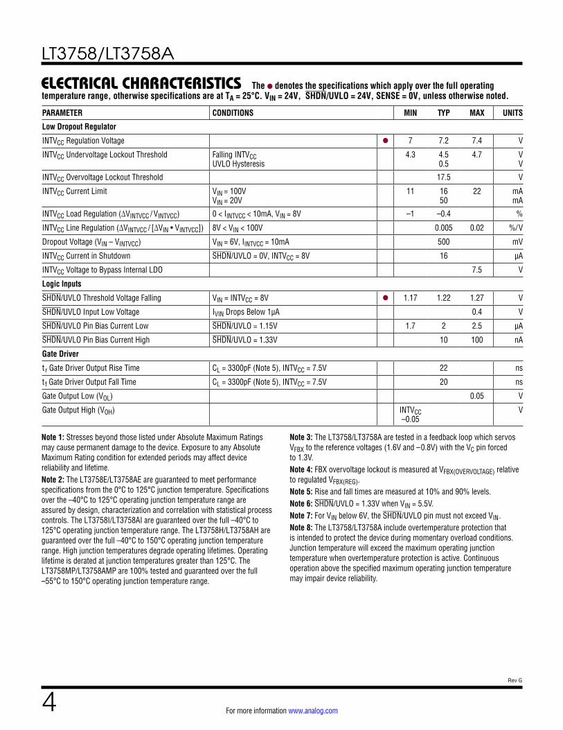
ELECTRICAL CHARACTERISTICS The l denotes the specifications which apply over the full operating temperature range, otherwise specifications are at TA = 25°C. VIN = 24V, SHDN/UVLO = 24V, SENSE = 0V, unless otherwise noted.
PARAMETER CONDITIONS MIN TYP MAX UNITS
Low Dropout Regulator
INTVCC Regulation Voltage l 7 7.2 7.4 V
INTVCC Undervoltage Lockout Threshold Falling INTVCC UVLO Hysteresis
4.3 4.5 0.5
4.7 V V
INTVCC Overvoltage Lockout Threshold 17.5 V
INTVCC Current Limit VIN = 100V VIN = 20V
11 16 50
22 mA mA
INTVCC Load Regulation (∆VINTVCC / VINTVCC) 0 < IINTVCC < 10mA, VIN = 8V –1 –0.4 %
INTVCC Line Regulation (∆VINTVCC / [∆VIN • VINTVCC]) 8V < VIN < 100V 0.005 0.02 %/V
Dropout Voltage (VIN – VINTVCC) VIN = 6V, IINTVCC = 10mA 500 mV
INTVCC Current in Shutdown SHDN/UVLO = 0V, INTVCC = 8V 16 µA
INTVCC Voltage to Bypass Internal LDO 7.5 V
Logic Inputs
SHDN/UVLO Threshold Voltage Falling VIN = INTVCC = 8V l 1.17 1.22 1.27 V
SHDN/UVLO Input Low Voltage IVIN Drops Below 1µA 0.4 V
SHDN/UVLO Pin Bias Current Low SHDN/UVLO = 1.15V 1.7 2 2.5 µA
SHDN/UVLO Pin Bias Current High SHDN/UVLO = 1.33V 10 100 nA
Gate Driver
t r Gate Driver Output Rise Time CL = 3300pF (Note 5), INTVCC = 7.5V 22 ns
t f Gate Driver Output Fall Time CL = 3300pF (Note 5), INTVCC = 7.5V 20 ns
Gate Output Low (VOL) 0.05 V
Gate Output High (VOH) INTVCC –0.05
V
Note 1: Stresses beyond those listed under Absolute Maximum Ratings may cause permanent damage to the device. Exposure to any Absolute Maximum Rating condition for extended periods may affect device reliability and lifetime.Note 2: The LT3758E/LT3758AE are guaranteed to meet performance specifications from the 0°C to 125°C junction temperature. Specifications over the –40°C to 125°C operating junction temperature range are assured by design, characterization and correlation with statistical process controls. The LT3758I/LT3758AI are guaranteed over the full –40°C to 125°C operating junction temperature range. The LT3758H/LT3758AH are guaranteed over the full –40°C to 150°C operating junction temperature range. High junction temperatures degrade operating lifetimes. Operating lifetime is derated at junction temperatures greater than 125°C. The LT3758MP/LT3758AMP are 100% tested and guaranteed over the full –55°C to 150°C operating junction temperature range.
Note 3: The LT3758/LT3758A are tested in a feedback loop which servos VFBX to the reference voltages (1.6V and –0.8V) with the VC pin forced to 1.3V.Note 4: FBX overvoltage lockout is measured at VFBX(OVERVOLTAGE) relative to regulated VFBX(REG).Note 5: Rise and fall times are measured at 10% and 90% levels.Note 6: SHDN/UVLO = 1.33V when VIN = 5.5V.Note 7: For VIN below 6V, the SHDN/UVLO pin must not exceed VIN.Note 8: The LT3758/LT3758A include overtemperature protection that is intended to protect the device during momentary overload conditions. Junction temperature will exceed the maximum operating junction temperature when overtemperature protection is active. Continuous operation above the specified maximum operating junction temperature may impair device reliability.
LT3758/LT3758A
5Rev G
For more information www.analog.com
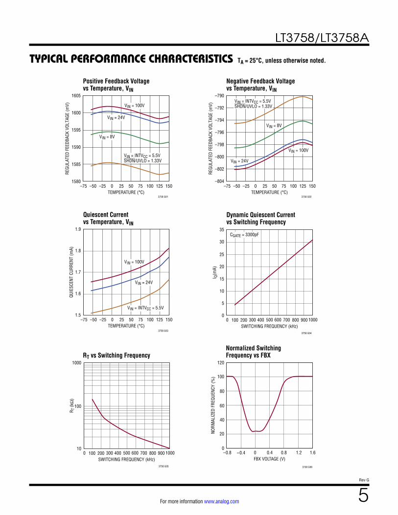
TEMPERATURE (°C)–75 –50
1580
1585
REGU
LATE
D FE
EDBA
CK V
OLTA
GE (m
V)
1590
1605
1600
0 50 75
1595
–25 25 100 150125
3758 G01
VIN = 100V
VIN = 24V
VIN = 8V
VIN = INTVCC = 5.5VSHDN/UVLO = 1.33V
TEMPERATURE (°C)
REGU
LATE
D FE
EDBA
CK V
OLTA
GE (m
V)
–802
–800
–798
–790
–792
–794
–804
–796
3758 G02
–75 –50 0 50 75–25 25 100 150125
VIN = 100V
VIN = 24V
VIN = 8V
VIN = INTVCC = 5.5VSHDN/UVLO = 1.33V
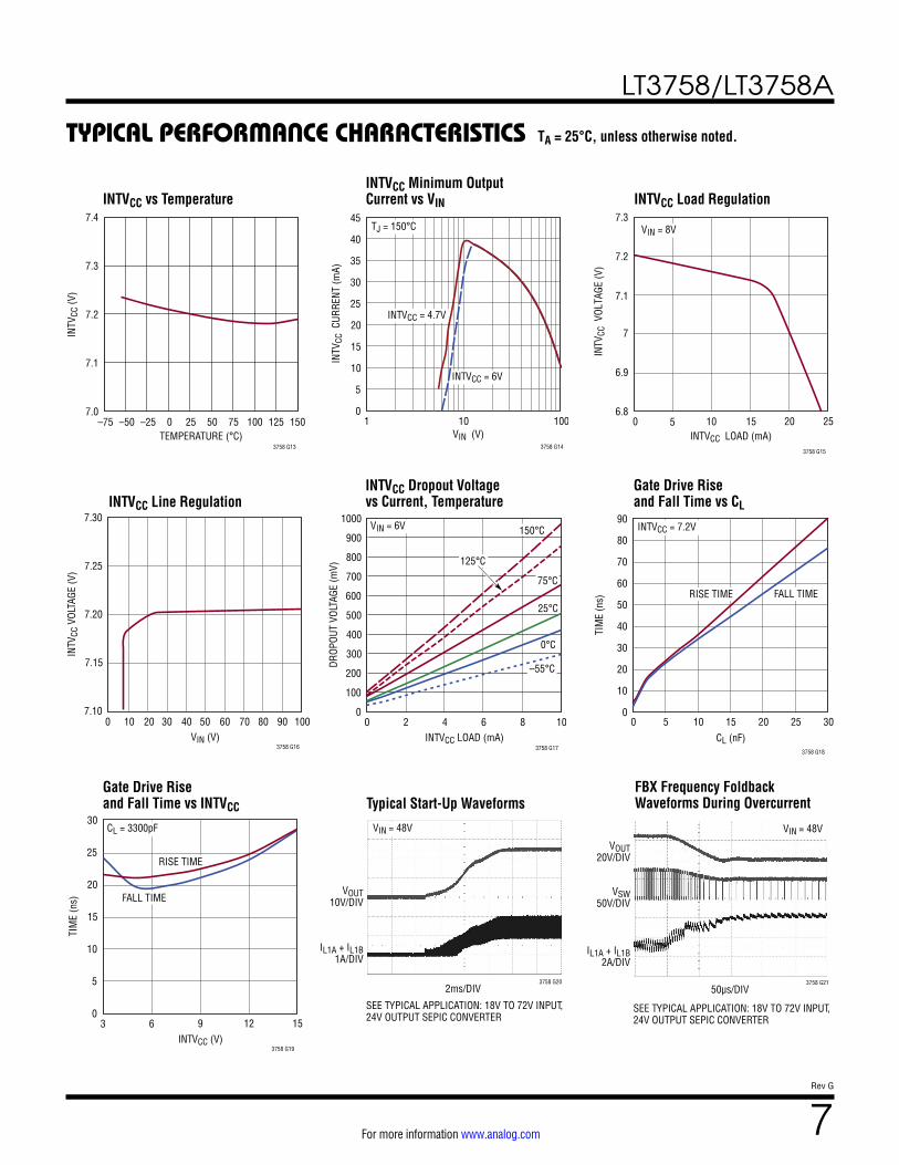
TYPICAL PERFORMANCE CHARACTERISTICS
Positive Feedback Voltage vs Temperature, VIN
Negative Feedback Voltage vs Temperature, VIN
Quiescent Current vs Temperature, VIN
TA = 25°C, unless otherwise noted.
–75 –50 0 50 75–25 25 100 150125TEMPERATURE (°C)
1.5
QUIE
SCEN
T CU
RREN
T (m
A)
1.6
1.9
1.8
1.7
3758 G03
VIN = 100V
VIN = 24V
VIN = INTVCC = 5.5V
Dynamic Quiescent Current vs Switching Frequency
RT vs Switching FrequencyNormalized Switching Frequency vs FBX
FBX VOLTAGE (V)–0.8
0
NORM
ALIZ
ED F
REQU
ENCY
(%)
20
40
60
80
120
–0.4 0 0.4 0.8
3758 G06
1.2 1.6
100
SWITCHING FREQUENCY (kHz)0
0
I Q(m
A)
15
20
35
300 500 600 700
10
5
25
30
100 200 400 900800 1000
3758 G04
CGATE = 3300pF
SWITCHING FREQUENCY (kHz)0
10
R T (k
Ω)
100
1000
300 500 600 700100 200 400 900800 1000
3758 G05
LT3758/LT3758A
6Rev G
For more information www.analog.com
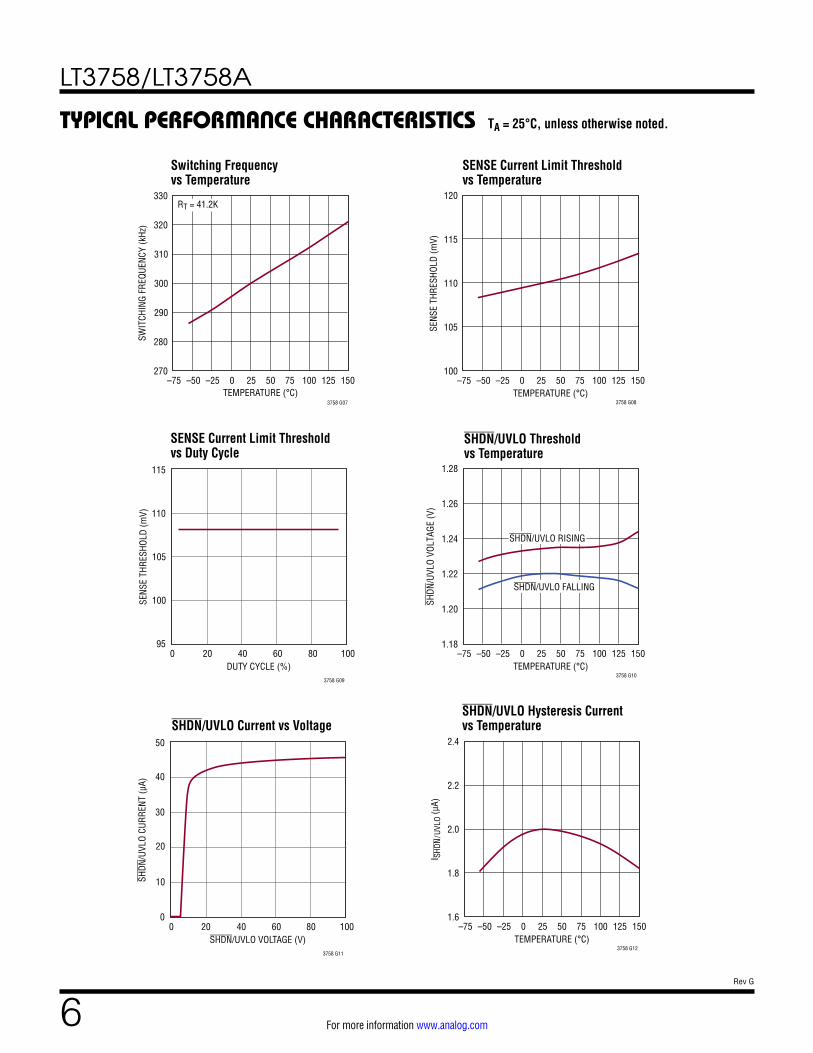
Switching Frequency vs Temperature
SENSE Current Limit Threshold vs Temperature
SENSE Current Limit Threshold vs Duty Cycle
SHDN/UVLO Threshold vs Temperature
SHDN/UVLO Current vs VoltageSHDN/UVLO Hysteresis Current vs Temperature
–75 –50 0 50 75–25 25 100 150125TEMPERATURE (°C)
100
SENS
E TH
RESH
OLD
(mV)
105
110
115
120
3758 G08
DUTY CYCLE (%)0
95
SENS
E TH
RESH
OLD
(mV)
105
20 40 8060
115
100
110
100
3758 G09
SHDN/UVLO VOLTAGE (V)0
0
SHDN
/UVL
O CU
RREN
T (µ
A)
20
20 6040 80
40
50
10
30
100
3758 G11
–75 –50 0 50 75–25 25 100 150125TEMPERATURE (°C)
1.6
I SHD
N/U
VLO
(µA)
1.8
2.0
2.2
2.4
3758 G12
–75 –50 0 50 75–25 25 100 150125TEMPERATURE (°C)
270
SWIT
CHIN
G FR
EQUE
NCY
(kHz
)
280
290
300
310
330
3758 G07
320
RT = 41.2K
–75 –50 0 50 75–25 25 100 150125TEMPERATURE (°C)
1.18
SHDN
/UVL
O VO
LTAG
E (V
)
1.22
1.24
1.26
1.28
1.20
3758 G10
SHDN/UVLO FALLING
SHDN/UVLO RISING
TYPICAL PERFORMANCE CHARACTERISTICS TA = 25°C, unless otherwise noted.
LT3758/LT3758A
7Rev G
For more information www.analog.com
TYPICAL PERFORMANCE CHARACTERISTICS TA = 25°C, unless otherwise noted.
INTVCC Line RegulationINTVCC Dropout Voltage vs Current, Temperature
INTVCC vs TemperatureINTVCC Minimum Output Current vs VIN INTVCC Load Regulation
–75 –50 0 50 75–25 25 100 150125TEMPERATURE (°C)
7.0
INTV
CC (V
)
7.1
7.2
7.3
7.4
3758 G13
VIN (V)0
INTV
CC V
OLTA
GE (V
)
90
7.25
7.20
20 30 5010 40 60 70 80 100
7.15
7.10
7.30
3758 G16
10
5
10
20
30
10 100
45
40
15
25
35
TJ = 150°C
VIN (V)3758 G14
INTV
CC C
URRE
NT (m
A)
INTVCC = 6V
INTVCC = 4.7V
INTVCC LOAD (mA)0
6.8
7
7.1
7.2
7.3
10 20 25
6.9
5 15
3758 G15
INTV
CC V
OLTA
GE (V
)
VIN = 8V
0 42 6 8 10INTVCC LOAD (mA)
DROP
OUT
VOLT
AGE
(mV)
500
600
300
400
200
100
0
1000
900
800
700
3758 G17
150°C
25°C
0°C
–55°C
75°C
VIN = 6V
125°C
Gate Drive Rise and Fall Time vs INTVCC Typical Start-Up Waveforms
FBX Frequency Foldback Waveforms During Overcurrent
INTVCC (V)3
TIM
E (n
s)
20
25
15
10
96 12 15
5
0
30
3758 G19
CL = 3300pF
RISE TIME
FALL TIME
2ms/DIV
SEE TYPICAL APPLICATION: 18V TO 72V INPUT, 24V OUTPUT SEPIC CONVERTER
VOUT10V/DIV
IL1A + IL1B1A/DIV
3758 G20
VIN = 48V
50µs/DIV
VOUT20V/DIV
VSW50V/DIV
IL1A + IL1B2A/DIV
3758 G21
VIN = 48V
SEE TYPICAL APPLICATION: 18V TO 72V INPUT, 24V OUTPUT SEPIC CONVERTER
Gate Drive Rise and Fall Time vs CL
CL (nF)0
TIM
E (n
s)60
70
80
50
40
5 1510 20 25 30
10
0
30
90
20
3758 G18
RISE TIME
INTVCC = 7.2V
FALL TIME
LT3758/LT3758A
8Rev G
For more information www.analog.com
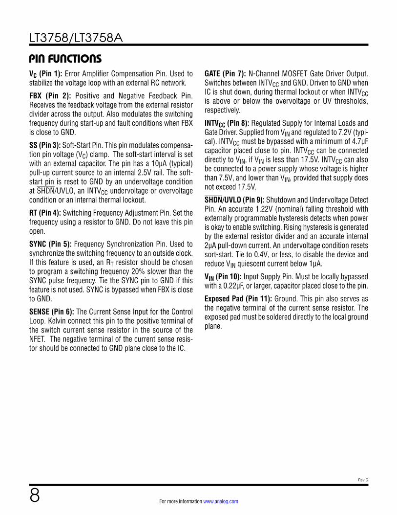
PIN FUNCTIONSVC (Pin 1): Error Amplifier Compensation Pin. Used to stabilize the voltage loop with an external RC network.
FBX (Pin 2): Positive and Negative Feedback Pin. Receives the feedback voltage from the external resistor divider across the output. Also modulates the switching frequency during start-up and fault conditions when FBX is close to GND.
SS (Pin 3): Soft-Start Pin. This pin modulates compensa-tion pin voltage (VC) clamp. The soft-start interval is set with an external capacitor. The pin has a 10µA (typical) pull-up current source to an internal 2.5V rail. The soft-start pin is reset to GND by an undervoltage condition at SHDN/UVLO, an INTVCC undervoltage or overvoltage condition or an internal thermal lockout.
RT (Pin 4): Switching Frequency Adjustment Pin. Set the frequency using a resistor to GND. Do not leave this pin open.
SYNC (Pin 5): Frequency Synchronization Pin. Used to synchronize the switching frequency to an outside clock. If this feature is used, an RT resistor should be chosen to program a switching frequency 20% slower than the SYNC pulse frequency. Tie the SYNC pin to GND if this feature is not used. SYNC is bypassed when FBX is close to GND.
SENSE (Pin 6): The Current Sense Input for the Control Loop. Kelvin connect this pin to the positive terminal of the switch current sense resistor in the source of the NFET. The negative terminal of the current sense resis-tor should be connected to GND plane close to the IC.
GATE (Pin 7): N-Channel MOSFET Gate Driver Output. Switches between INTVCC and GND. Driven to GND when IC is shut down, during thermal lockout or when INTVCC is above or below the overvoltage or UV thresholds, respectively.
INTVCC (Pin 8): Regulated Supply for Internal Loads and Gate Driver. Supplied from VIN and regulated to 7.2V (typi-cal). INTVCC must be bypassed with a minimum of 4.7µF capacitor placed close to pin. INTVCC can be connected directly to VIN, if VIN is less than 17.5V. INTVCC can also be connected to a power supply whose voltage is higher than 7.5V, and lower than VIN, provided that supply does not exceed 17.5V.
SHDN/UVLO (Pin 9): Shutdown and Undervoltage Detect Pin. An accurate 1.22V (nominal) falling threshold with externally programmable hysteresis detects when power is okay to enable switching. Rising hysteresis is generated by the external resistor divider and an accurate internal 2µA pull-down current. An undervoltage condition resets sort-start. Tie to 0.4V, or less, to disable the device and reduce VIN quiescent current below 1µA.
VIN (Pin 10): Input Supply Pin. Must be locally bypassed with a 0.22µF, or larger, capacitor placed close to the pin.
Exposed Pad (Pin 11): Ground. This pin also serves as the negative terminal of the current sense resistor. The exposed pad must be soldered directly to the local ground plane.
LT3758/LT3758A
9Rev G
For more information www.analog.com
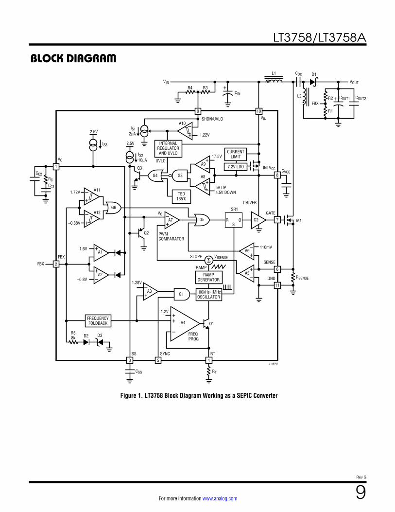
BLOCK DIAGRAM
Figure 1. LT3758 Block Diagram Working as a SEPIC Converter
L1
R1
R3R4
M1
R2L2
FBX
1.22V
2.5V
D1CDC
CIN
VOUT
COUT2COUT1
CVCCINTVCC
VIN
RSENSE
VISENSE
•+
+VIN
IS12µA
10
8
7
1
9
SHDN/UVLO
INTERNALREGULATORAND UVLO
TSD165˚C
A10
Q3
VC
17.5V
5V UP4.5V DOWN
A8
UVLOIS210µA
IS3
CC1
CC2RC
DRIVER
SLOPESENSE
GND
GATE
110mV
SR1
+–
+–
CURRENTLIMIT
RAMPGENERATOR
7.2V LDO
•
+–
+–
R OS
2.5V
RT
RT
SS
CSS
SYNC
1.28V
1.2V
FBX
FBX
1.6V
–0.8V
+–
+–
2
3 5 4
+–
+–
6
11
RAMP
PWMCOMPARATOR
FREQUENCYFOLDBACK
100kHz-1MHzOSCILLATOR
FREQPROG
3758 F01
–
++ Q1
A1
A2
1.72V
–0.88V
+–
+–
A11
A12
+–
A3
A4
A5
A6
G2G5
G6
A7
A9
Q2
G4 G3
G1
VC
D2R58k D3
LT3758/LT3758A
10Rev G
For more information www.analog.com
APPLICATIONS INFORMATIONMain Control Loop
The LT3758 uses a fixed frequency, current mode con-trol scheme to provide excellent line and load regulation. Operation can be best understood by referring to the Block Diagram in Figure 1.
The start of each oscillator cycle sets the SR latch (SR1) and turns on the external power MOSFET switch M1 through driver G2. The switch current flows through the external current sensing resistor RSENSE and generates a voltage proportional to the switch current. This current sense voltage VISENSE (amplified by A5) is added to a stabilizing slope compensation ramp and the resulting sum (SLOPE) is fed into the positive terminal of the PWM comparator A7. When SLOPE exceeds the level at the negative input of A7 (VC pin), SR1 is reset, turning off the power switch. The level at the negative input of A7 is set by the error amplifier A1 (or A2) and is an amplified ver-sion of the difference between the feedback voltage (FBX pin) and the reference voltage (1.6V or –0.8V, depending on the configuration). In this manner, the error ampli-fier sets the correct peak switch current level to keep the output in regulation.
The LT3758 has a switch current limit function. The cur-rent sense voltage is input to the current limit compara-tor A6. If the SENSE pin voltage is higher than the sense current limit threshold VSENSE(MAX) (110mV, typical), A6 will reset SR1 and turn off M1 immediately.
The LT3758 is capable of generating either positive or negative output voltage with a single FBX pin. It can be configured as a boost, flyback or SEPIC converter to gen-erate positive output voltage, or as an inverting converter to generate negative output voltage. When configured as a SEPIC converter, as shown in Figure 1, the FBX pin is pulled up to the internal bias voltage of 1.6V by a volt-age divider (R1 and R2) connected from VOUT to GND. Comparator A2 becomes inactive and comparator A1 per-forms the inverting amplification from FBX to VC. When the LT3758 is in an inverting configuration, the FBX pin is pulled down to –0.8V by a voltage divider connected from VOUT to GND. Comparator A1 becomes inactive and comparator A2 performs the noninverting amplification from FBX to VC.
The LT3758 has overvoltage protection functions to pro-tect the converter from excessive output voltage over-shoot during start-up or recovery from a short-circuit condition. An overvoltage comparator A11 (with 20mV hysteresis) senses when the FBX pin voltage exceeds the positive regulated voltage (1.6V) by 8% and provides a reset pulse. Similarly, an overvoltage comparator A12 (with 10mV hysteresis) senses when the FBX pin voltage exceeds the negative regulated voltage (–0.8V) by 11% and provides a reset pulse. Both reset pulses are sent to the main RS latch (SR1) through G6 and G5. The power MOSFET switch M1 is actively held off for the duration of an output overvoltage condition.
Programming Turn-On and Turn-Off Thresholds with the SHDN/UVLO Pin
The SHDN/UVLO pin controls whether the LT3758 is enabled or is in shutdown state. A micropower 1.22V reference, a comparator A10 and a controllable current source IS1 allow the user to accurately program the supply voltage at which the IC turns on and off. The falling value can be accurately set by the resistor dividers R3 and R4. When SHDN/UVLO is above 0.4V, and below the 1.22V threshold, the small pull-down current source IS1 (typical 2µA) is active.
The purpose of this current is to allow the user to program the rising hysteresis. The Block Diagram of the compara-tor and the external resistors is shown in Figure 1. The typical falling threshold voltage and rising threshold volt-age can be calculated by the following equations:
VVIN,FALLING = 1.22 •(R3+R4)
R4VVIN,RISING = 2µA •R3+ VIN,FALLING
For applications where the SHDN/UVLO pin is only used as a logic input, the SHDN/UVLO pin can be connected directly to the input voltage VIN through a 1k resistor for always-on operation.
LT3758/LT3758A
11Rev G
For more information www.analog.com
APPLICATIONS INFORMATIONINTVCC Regulator Bypassing and Operation
An internal, low dropout (LDO) voltage regulator produces the 7.2V INTVCC supply which powers the gate driver, as shown in Figure 1. The LT3758 contains an undervoltage lockout comparator A8 and an overvoltage lockout com-parator A9 for the INTVCC supply. The INTVCC undervoltage (UV) threshold is 4.5V (typical), with 0.5V hysteresis, to ensure that the MOSFETs have sufficient gate drive voltage before turning on. The logic circuitry within the LT3758 is also powered from the internal INTVCC supply.
The INTVCC overvoltage threshold is set to be 17.5V (typical) to protect the gate of the power MOSFET. When INTVCC is below the UV threshold, or above the overvolt-age threshold, the GATE pin will be forced to GND and the soft-start operation will be triggered.
The INTVCC regulator must be bypassed to ground imme-diately adjacent to the IC pins with a minimum of 4.7µF ceramic capacitor. Good bypassing is necessary to sup-ply the high transient currents required by the MOSFET gate driver.
In an actual application, most of the IC supply current is used to drive the gate capacitance of the power MOSFET. The on-chip power dissipation can be a significant con-cern when a large power MOSFET is being driven at a high frequency and the VIN voltage is high. It is impor-tant to limit the power dissipation through selection of MOSFET and/or operating frequency so the LT3758 does not exceed its maximum junction temperature rating. The junction temperature TJ can be estimated using the fol-lowing equations:
TJ = TA + PIC • θJA
TA = ambient temperature
θJA = junction-to-ambient thermal resistance
PIC = IC power consumption
= VIN • (IQ + IDRIVE)
IQ = VIN operation IQ = 1.6mA
IDRIVE = average gate drive current = f • QG
f = switching frequency
QG = power MOSFET total gate charge
The LT3758 uses packages with an Exposed Pad for enhanced thermal conduction. With proper soldering to the Exposed Pad on the underside of the package and a full copper plane underneath the device, thermal resis-tance (θJA) will be about 43°C/W for the DD package and 40°C/W for the MSE package. For an ambient board tem-perature of TA = 70°C and maximum junction temperature of 125°C, the maximum IDRIVE (IDRIVE(MAX)) of the DD package can be calculated as:
IDRIVE(MAX)=
(TJ−TA)(θJA • VIN)
−IQ = 1.28WVIN
−1.6mA
The LT3758 has an internal INTVCC IDRIVE current limit function to protect the IC from excessive on-chip power dissipation. The IDRIVE current limit decreases as the VIN increases (see the INTVCC Minimum Output Current vs VIN graph in the Typical Performance Characteristics section). If IDRIVE reaches the current limit, INTVCC voltage will fall and may trigger the soft-start.
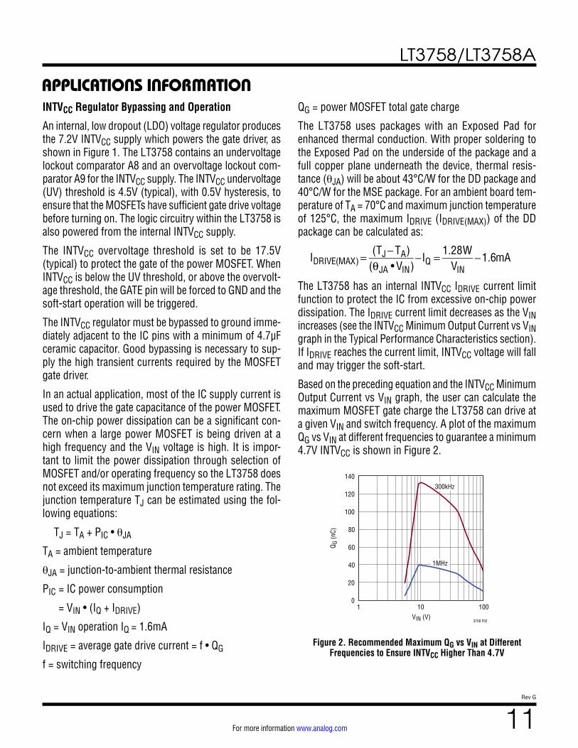
Based on the preceding equation and the INTVCC Minimum Output Current vs VIN graph, the user can calculate the maximum MOSFET gate charge the LT3758 can drive at a given VIN and switch frequency. A plot of the maximum QG vs VIN at different frequencies to guarantee a minimum 4.7V INTVCC is shown in Figure 2.
Figure 2. Recommended Maximum QG vs VIN at Different Frequencies to Ensure INTVCC Higher Than 4.7V
VIN (V)1
Q G (n
C)
10 100
3758 F02
0
20
40
80
120
140
60
100
300kHz
1MHz
LT3758/LT3758A
12Rev G
For more information www.analog.com
APPLICATIONS INFORMATIONAs illustrated in Figure 2, a trade-off between the operat-ing frequency and the size of the power MOSFET may be needed in order to maintain a reliable IC junction tempera-ture. Prior to lowering the operating frequency, however, be sure to check with power MOSFET manufacturers for their most recent low QG, low RDS(ON) devices. Power MOSFET manufacturing technologies are continually improving, with newer and better performance devices being introduced almost yearly.
An effective approach to reduce the power consumption of the internal LDO for gate drive is to tie the INTVCC pin to an external voltage source high enough to turn off the internal LDO regulator.
If the input voltage VIN does not exceed the absolute maxi-mum rating of both the power MOSFET gate-source volt-age (VGS) and the INTVCC overvoltage lockout threshold voltage (17.5V), the INTVCC pin can be shorted directly to the VIN pin. In this condition, the internal LDO will be turned off and the gate driver will be powered directly from the input voltage VIN. With the INTVCC pin shorted to VIN, however, a small current (around 16µA) will load the INTVCC in shutdown mode. For applications that require the lowest shutdown mode input supply current, do not connect the INTVCC pin to VIN.
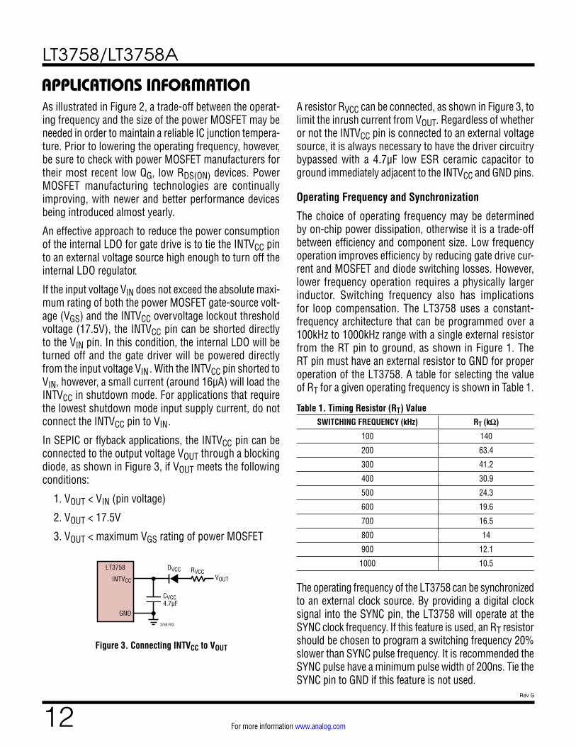
In SEPIC or flyback applications, the INTVCC pin can be connected to the output voltage VOUT through a blocking diode, as shown in Figure 3, if VOUT meets the following conditions:
1. VOUT < VIN (pin voltage)
2. VOUT < 17.5V
3. VOUT < maximum VGS rating of power MOSFET
A resistor RVCC can be connected, as shown in Figure 3, to limit the inrush current from VOUT. Regardless of whether or not the INTVCC pin is connected to an external voltage source, it is always necessary to have the driver circuitry bypassed with a 4.7µF low ESR ceramic capacitor to ground immediately adjacent to the INTVCC and GND pins.
Operating Frequency and Synchronization
The choice of operating frequency may be determined by on-chip power dissipation, otherwise it is a trade-off between efficiency and component size. Low frequency operation improves efficiency by reducing gate drive cur-rent and MOSFET and diode switching losses. However, lower frequency operation requires a physically larger inductor. Switching frequency also has implications for loop compensation. The LT3758 uses a constant-frequency architecture that can be programmed over a 100kHz to 1000kHz range with a single external resistor from the RT pin to ground, as shown in Figure 1. The RT pin must have an external resistor to GND for proper operation of the LT3758. A table for selecting the value of RT for a given operating frequency is shown in Table 1.
Table 1. Timing Resistor (RT) ValueSWITCHING FREQUENCY (kHz) RT (kΩ)
100 140
200 63.4
300 41.2
400 30.9
500 24.3
600 19.6
700 16.5
800 14
900 12.1
1000 10.5
The operating frequency of the LT3758 can be synchronized to an external clock source. By providing a digital clock signal into the SYNC pin, the LT3758 will operate at the SYNC clock frequency. If this feature is used, an RT resistor should be chosen to program a switching frequency 20% slower than SYNC pulse frequency. It is recommended the SYNC pulse have a minimum pulse width of 200ns. Tie the SYNC pin to GND if this feature is not used.
Figure 3. Connecting INTVCC to VOUT
CVCC4.7µF
VOUT
3758 F03
INTVCC
GND
LT3758 RVCCDVCC
LT3758/LT3758A
13Rev G
For more information www.analog.com
APPLICATIONS INFORMATIONDuty Cycle Consideration
Switching duty cycle is a key variable defining con-verter operation. As such, its limits must be considered. Minimum on-time is the smallest time duration that the LT3758 is capable of turning on the power MOSFET. This time is generally about 220ns (typical) (see Minimum On-Time in the Electrical Characteristics table). In each switching cycle, the LT3758 keeps the power switch off for at least 220ns (typical) (see Minimum Off-Time in the Electrical Characteristics table).
The minimum on-time and minimum off-time and the switching frequency define the minimum and maximum switching duty cycles a converter is able to generate:
Minimum duty cycle = minimum on-time • frequency
Maximum duty cycle = 1 – (minimum off-time • frequency)
Programming the Output Voltage
The output voltage VOUT is set by a resistor divider, as shown in Figure 1. The positive and negative VOUT are set by the following equations:
VOUT,POSITIVE =1.6V • 1+R2R1
⎛⎝⎜
⎞⎠⎟
VOUT,NEGATIVE = –0.8V • 1+R2R1
⎛⎝⎜
⎞⎠⎟
The resistors R1 and R2 are typically chosen so that the error caused by the current flowing into the FBX pin during normal operation is less than 1% (this translates to a maximum value of R1 at about 158k).
In the applications where VOUT is pulled up by an exter-nal positive power supply, the FBX pin is also pulled up through the R2 and R1 network. Make sure the FBX does not exceed its absolute maximum rating (6V). The R5, D2, and D3 in Figure 1 provide a resistive clamp in the positive direction. To ensure FBX is lower than 6V, choose suf-ficiently large R1 and R2 to meet the following condition:
6V • 1+ R2
R1⎛⎝⎜
⎞⎠⎟ + 3.5V •
R28kΩ
> VOUT(MAX)
where VOUT(MAX) is the maximum VOUT that is pulled up by an external power supply.
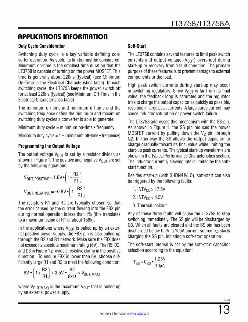
Soft-Start
The LT3758 contains several features to limit peak switch currents and output voltage (VOUT) overshoot during start-up or recovery from a fault condition. The primary purpose of these features is to prevent damage to external components or the load.
High peak switch currents during start-up may occur in switching regulators. Since VOUT is far from its final value, the feedback loop is saturated and the regulator tries to charge the output capacitor as quickly as possible, resulting in large peak currents. A large surge current may cause inductor saturation or power switch failure.
The LT3758 addresses this mechanism with the SS pin. As shown in Figure 1, the SS pin reduces the power MOSFET current by pulling down the VC pin through Q2. In this way the SS allows the output capacitor to charge gradually toward its final value while limiting the start-up peak currents. The typical start-up waveforms are shown in the Typical Performance Characteristics section. The inductor current IL slewing rate is limited by the soft-start function.
Besides start-up (with SHDN/UVLO), soft-start can also be triggered by the following faults:
1. INTVCC > 17.5V
2. INTVCC < 4.5V
3. Thermal lockout
Any of these three faults will cause the LT3758 to stop switching immediately. The SS pin will be discharged by Q3. When all faults are cleared and the SS pin has been discharged below 0.2V, a 10µA current source IS2 starts charging the SS pin, initiating a soft-start operation.
The soft-start interval is set by the soft-start capacitor selection according to the equation:
TSS = CSS •
1.25V10µA
LT3758/LT3758A
14Rev G
For more information www.analog.com
APPLICATIONS INFORMATIONFBX Frequency Foldback
When VOUT is very low during start-up or a GND fault on the output, the switching regulator must operate at low duty cycles to maintain the power switch current within the current limit range, since the inductor cur-rent decay rate is very low during switch off time. The minimum on-time limitation may prevent the switcher from attaining a sufficiently low duty cycle at the pro-grammed switching frequency. So, the switch current will keep increasing through each switch cycle, exceed-ing the programmed current limit. To prevent the switch peak currents from exceeding the programmed value, the LT3758 contains a frequency foldback function to reduce the switching frequency when the FBX voltage is low (see the Normalized Switching Frequency vs FBX graph in the Typical Performance Characteristics section).
During frequency foldback, external clock synchroniza-tion is disabled to prevent interference with frequency reducing operation.
Thermal Lockout
If LT3758 die temperature reaches 165°C (typical), the part will go into thermal lockout. The power switch will be turned off. A soft-start operation will be triggered. The part will be enabled again when the die temperature has dropped by 5°C (nominal).
Loop Compensation
Loop compensation determines the stability and transient performance. The LT3758/LT3758A use current mode control to regulate the output which simplifies loop com-pensation. The LT3758A improves the no-load to heavy
load transient response, when compared to the LT3758. New internal circuits ensure that the transient from not switching to switching at high current can be made in a few cycles. The optimum values depend on the con-verter topology, the component values and the operat-ing conditions (including the input voltage, load current, etc.). To compensate the feedback loop of the LT3758/LT3758A, a series resistor-capacitor network is usually connected from the VC pin to GND. Figure 1 shows the typical VC compensation network. For most applications, the capacitor should be in the range of 470pF to 22nF, and the resistor should be in the range of 5k to 50k. A small capacitor is often connected in parallel with the RC compensation network to attenuate the VC voltage ripple induced from the output voltage ripple through the inter-nal error amplifier. The parallel capacitor usually ranges in value from 10pF to 100pF. A practical approach to design the compensation network is to start with one of the cir-cuits in this data sheet that is similar to your applica-tion, and tune the compensation network to optimize the performance. Stability should then be checked across all operating conditions, including load current, input voltage and temperature.
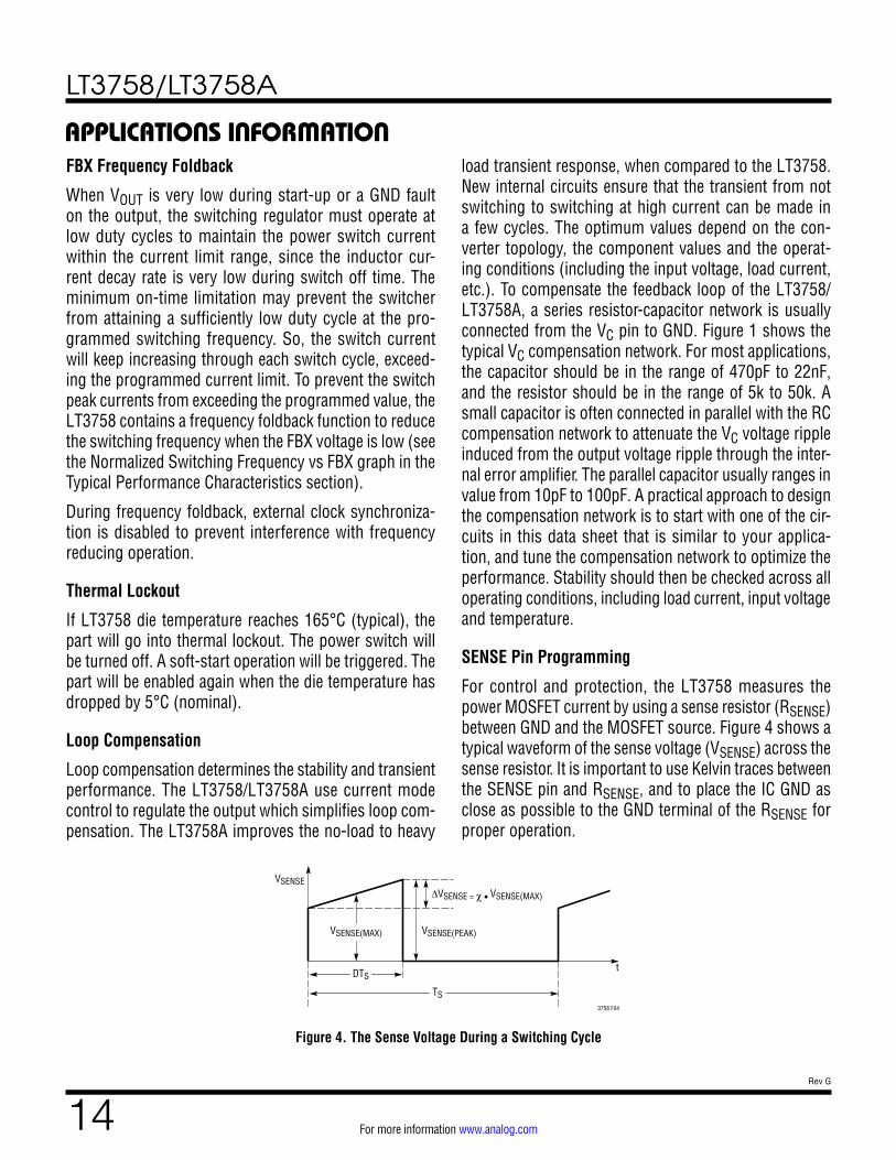
SENSE Pin Programming
For control and protection, the LT3758 measures the power MOSFET current by using a sense resistor (RSENSE) between GND and the MOSFET source. Figure 4 shows a typical waveform of the sense voltage (VSENSE) across the sense resistor. It is important to use Kelvin traces between the SENSE pin and RSENSE, and to place the IC GND as close as possible to the GND terminal of the RSENSE for proper operation.
Figure 4. The Sense Voltage During a Switching Cycle
3758 F04
VSENSE(PEAK)
∆VSENSE = χ • VSENSE(MAX)
VSENSE
tDTS
VSENSE(MAX)
TS
LT3758/LT3758A
15Rev G
For more information www.analog.com
APPLICATIONS INFORMATIONDue to the current limit function of the SENSE pin, RSENSE should be selected to guarantee that the peak current sense voltage VSENSE(PEAK) during steady state normal operation is lower than the SENSE current limit threshold (see the Electrical Characteristics table). Given a 20% margin, VSENSE(PEAK) is set to be 80mV. Then, the maximum switch ripple current percentage can be calculated using the following equation:
χ= ΔVSENSE
80mV−0.5•ΔVSENSEc is used in subsequent design examples to calculate inductor value. ∆VSENSE is the ripple voltage across RSENSE.
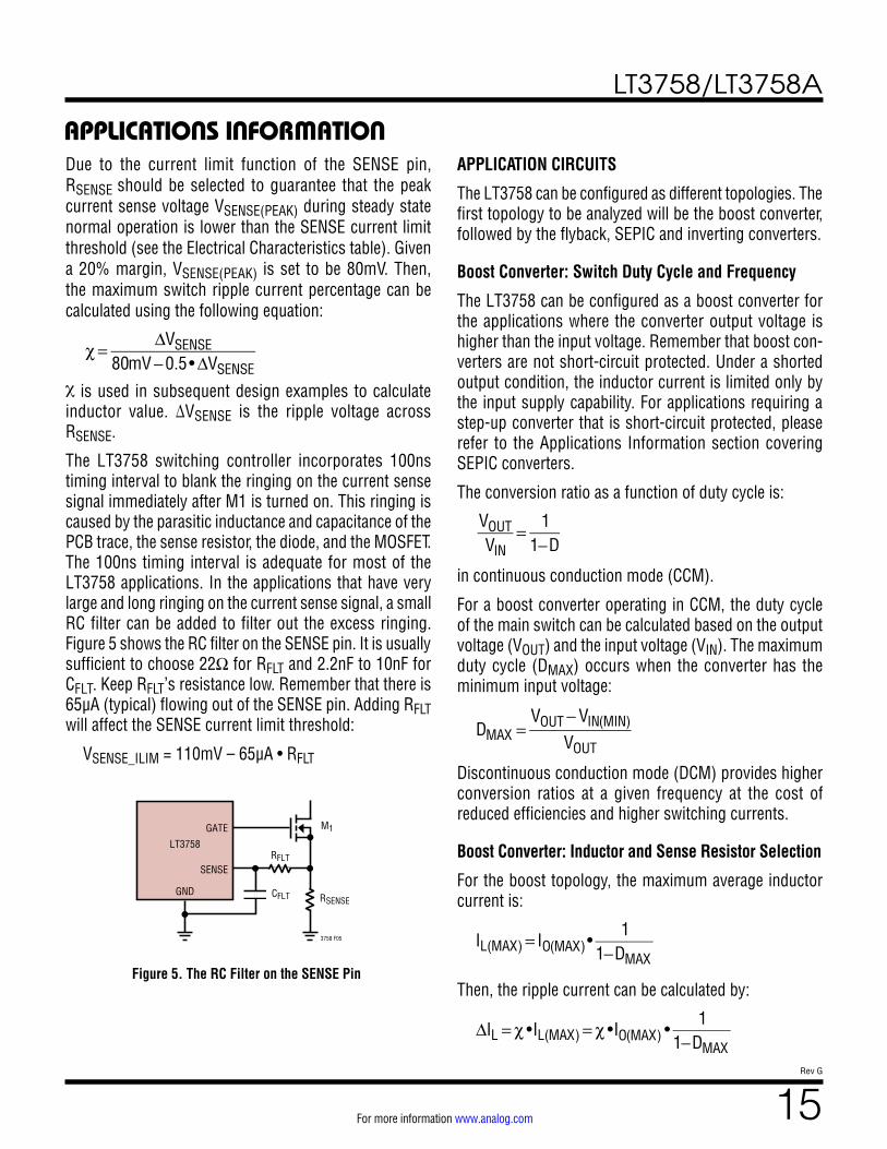
The LT3758 switching controller incorporates 100ns timing interval to blank the ringing on the current sense signal immediately after M1 is turned on. This ringing is caused by the parasitic inductance and capacitance of the PCB trace, the sense resistor, the diode, and the MOSFET. The 100ns timing interval is adequate for most of the LT3758 applications. In the applications that have very large and long ringing on the current sense signal, a small RC filter can be added to filter out the excess ringing. Figure 5 shows the RC filter on the SENSE pin. It is usually sufficient to choose 22Ω for RFLT and 2.2nF to 10nF for CFLT. Keep RFLT’s resistance low. Remember that there is 65µA (typical) flowing out of the SENSE pin. Adding RFLT will affect the SENSE current limit threshold:
VSENSE_ILIM = 110mV – 65µA • RFLT
APPLICATION CIRCUITS
The LT3758 can be configured as different topologies. The first topology to be analyzed will be the boost converter, followed by the flyback, SEPIC and inverting converters.
Boost Converter: Switch Duty Cycle and Frequency
The LT3758 can be configured as a boost converter for the applications where the converter output voltage is higher than the input voltage. Remember that boost con-verters are not short-circuit protected. Under a shorted output condition, the inductor current is limited only by the input supply capability. For applications requiring a step-up converter that is short-circuit protected, please refer to the Applications Information section covering SEPIC converters.
The conversion ratio as a function of duty cycle is:
VOUTVIN
= 11−D
in continuous conduction mode (CCM).
For a boost converter operating in CCM, the duty cycle of the main switch can be calculated based on the output voltage (VOUT) and the input voltage (VIN). The maximum duty cycle (DMAX) occurs when the converter has the minimum input voltage:
DMAX =
VOUT−VIN(MIN)
VOUTDiscontinuous conduction mode (DCM) provides higher conversion ratios at a given frequency at the cost of reduced efficiencies and higher switching currents.
Boost Converter: Inductor and Sense Resistor Selection
For the boost topology, the maximum average inductor current is:
IL(MAX)= IO(MAX)•
11−DMAX
Then, the ripple current can be calculated by:
ΔIL = χ •IL(MAX)= χ •IO(MAX) •1
1−DMAX
Figure 5. The RC Filter on the SENSE Pin
CFLT
3758 F05
LT3758RFLT
RSENSE
M1
SENSE
GATE
GND
LT3758/LT3758A
16Rev G
For more information www.analog.com
APPLICATIONS INFORMATIONThe constant c in the preceding equation represents the percentage peak-to-peak ripple current in the inductor, relative to IL(MAX).
The inductor ripple current has a direct effect on the choice of the inductor value. Choosing smaller values of ∆IL requires large inductances and reduces the current loop gain (the converter will approach voltage mode). Accepting larger values of ∆IL provides fast transient response and allows the use of low inductances, but results in higher input current ripple, greater core losses, and in some cases, subharmonic oscillation. A good starting point for c is 0.2 and careful evaluation of system stability should be made to ensure adequate design margin.
Given an operating input voltage range, and having cho-sen the operating frequency and ripple current in the inductor, the inductor value of the boost converter can be determined using the following equation:
L =
VIN(MIN)
ΔIL • f•DMAX
The peak and RMS inductor current are:
IL(PEAK)= IL(MAX) • 1+ χ2
⎛⎝⎜
⎞⎠⎟
IL(RMS)= IL(MAX) • 1+ χ2
12
Based on these equations, the user should choose the inductors having sufficient saturation and RMS current ratings.
Set the sense voltage at IL(PEAK) to be the minimum of the SENSE current limit threshold with a 20% margin. The sense resistor value can then be calculated to be:
RSENSE =
80mVIL(PEAK)
Boost Converter: Power MOSFET Selection
Important parameters for the power MOSFET include the drain-source voltage rating (VDS), the threshold voltage
(VGS(TH)), the on-resistance (RDS(ON)), the gate to source and gate to drain charges (QGS and QGD), the maximum drain current (ID(MAX)) and the MOSFET’s thermal resistances (RθJC and RθJA).
The power MOSFET will see full output voltage, plus a diode forward voltage, and any additional ringing across its drain-to-source during its off-time. It is recommended to choose a MOSFET whose BVDSS is higher than VOUT by a safety margin (a 10V safety margin is usually sufficient).
The power dissipated by the MOSFET in a boost converter is:
PFET = I2L(MAX) • RDS(ON) • DMAX + 2 • V2OUT • IL(MAX)
• CRSS • f/1A
The first term in the preceding equation represents the conduction losses in the device, and the second term, the switching loss. CRSS is the reverse transfer capacitance, which is usually specified in the MOSFET characteristics.
For maximum efficiency, RDS(ON) and CRSS should be minimized. From a known power dissipated in the power MOSFET, its junction temperature can be obtained using the following equation:
TJ = TA + PFET • θJA = TA + PFET • (θJC + θCA)
TJ must not exceed the MOSFET maximum junction temperature rating. It is recommended to measure the MOSFET temperature in steady state to ensure that abso-lute maximum ratings are not exceeded.
Boost Converter: Output Diode Selection
To maximize efficiency, a fast switching diode with low forward drop and low reverse leakage is desirable. The peak reverse voltage that the diode must withstand is equal to the regulator output voltage plus any additional ringing across its anode-to-cathode during the on-time. The average forward current in normal operation is equal to the output current, and the peak current is equal to:
ID(PEAK)= IL(PEAK)= 1+ χ2
⎛⎝⎜
⎞⎠⎟ •IL(MAX)
It is recommended that the peak repetitive reverse voltage rating VRRM is higher than VOUT by a safety margin (a 10V safety margin is usually sufficient).
LT3758/LT3758A
17Rev G
For more information www.analog.com
APPLICATIONS INFORMATION
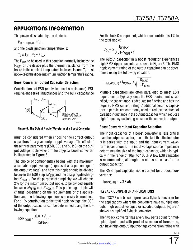
Figure 6. The Output Ripple Waveform of a Boost Converter
VOUT(AC)
tON
∆VESR
RINGING DUE TOTOTAL INDUCTANCE(BOARD + CAP)
∆VCOUT
3758 F06
tOFF
For the bulk C component, which also contributes 1% to the total ripple:
COUT ≥
IO(MAX)
0.01• VOUT • f
The output capacitor in a boost regulator experiences high RMS ripple currents, as shown in Figure 6. The RMS ripple current rating of the output capacitor can be deter-mined using the following equation:
IRMS(COUT)≥ IO(MAX) •
DMAX1−DMAX
Multiple capacitors are often paralleled to meet ESR requirements. Typically, once the ESR requirement is sat-isfied, the capacitance is adequate for filtering and has the required RMS current rating. Additional ceramic capaci-tors in parallel are commonly used to reduce the effect of parasitic inductance in the output capacitor, which reduces high frequency switching noise on the converter output.
Boost Converter: Input Capacitor Selection
The input capacitor of a boost converter is less critical than the output capacitor, due to the fact that the inductor is in series with the input, and the input current wave-form is continuous. The input voltage source impedance determines the size of the input capacitor, which is typi-cally in the range of 10µF to 100µF. A low ESR capacitor is recommended, although it is not as critical as for the output capacitor.
The RMS input capacitor ripple current for a boost con-verter is:
IRMS(CIN) = 0.3 • ∆IL
FLYBACK CONVERTER APPLICATIONS
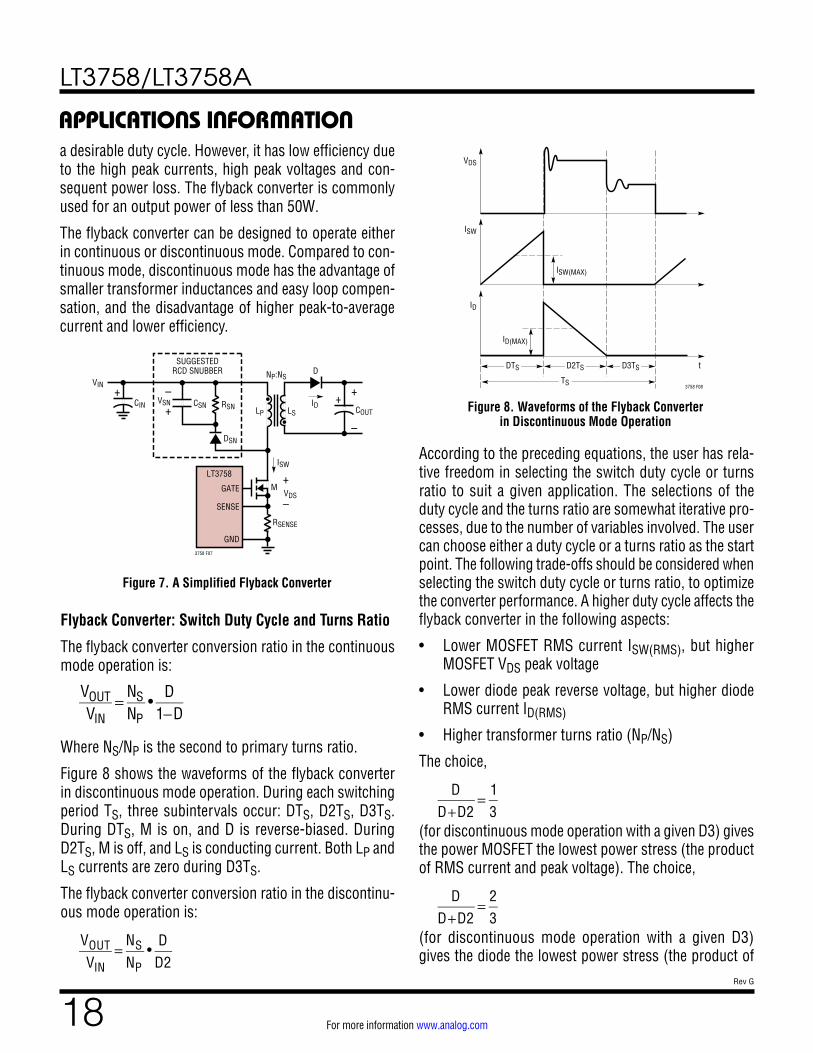
The LT3758 can be configured as a flyback converter for the applications where the converters have multiple out-puts, high output voltages or isolated outputs. Figure 7 shows a simplified flyback converter.
The flyback converter has a very low parts count for mul-tiple outputs, and with prudent selection of turns ratio, can have high output/input voltage conversion ratios with
The power dissipated by the diode is:
PD = IO(MAX) • VD
and the diode junction temperature is:
TJ = TA + PD • RθJA
The RθJA to be used in this equation normally includes the RθJC for the device plus the thermal resistance from the board to the ambient temperature in the enclosure. TJ must not exceed the diode maximum junction temperature rating.
Boost Converter: Output Capacitor Selection
Contributions of ESR (equivalent series resistance), ESL (equivalent series inductance) and the bulk capacitance
must be considered when choosing the correct output capacitors for a given output ripple voltage. The effect of these three parameters (ESR, ESL and bulk C) on the out-put voltage ripple waveform for a typical boost converter is illustrated in Figure 6.
The choice of component(s) begins with the maximum acceptable ripple voltage (expressed as a percentage of the output voltage), and how this ripple should be divided between the ESR step ∆VESR and the charging/discharg-ing ∆VCOUT. For the purpose of simplicity, we will choose 2% for the maximum output ripple, to be divided equally between ∆VESR and ∆VCOUT. This percentage ripple will change, depending on the requirements of the applica-tion, and the following equations can easily be modified. For a 1% contribution to the total ripple voltage, the ESR of the output capacitor can be determined using the fol-lowing equation:
ESRCOUT ≤
0.01• VOUTID(PEAK)
LT3758/LT3758A
18Rev G
For more information www.analog.com
APPLICATIONS INFORMATIONa desirable duty cycle. However, it has low efficiency due to the high peak currents, high peak voltages and con-sequent power loss. The flyback converter is commonly used for an output power of less than 50W.
The flyback converter can be designed to operate either in continuous or discontinuous mode. Compared to con-tinuous mode, discontinuous mode has the advantage of smaller transformer inductances and easy loop compen-sation, and the disadvantage of higher peak-to-average current and lower efficiency.
According to the preceding equations, the user has rela-tive freedom in selecting the switch duty cycle or turns ratio to suit a given application. The selections of the duty cycle and the turns ratio are somewhat iterative pro-cesses, due to the number of variables involved. The user can choose either a duty cycle or a turns ratio as the start point. The following trade-offs should be considered when selecting the switch duty cycle or turns ratio, to optimize the converter performance. A higher duty cycle affects the flyback converter in the following aspects:
• Lower MOSFET RMS current ISW(RMS), but higher MOSFET VDS peak voltage
• Lower diode peak reverse voltage, but higher diode RMS current ID(RMS)
• Higher transformer turns ratio (NP/NS)
The choice,
DD+D2
=13
(for discontinuous mode operation with a given D3) gives the power MOSFET the lowest power stress (the product of RMS current and peak voltage). The choice,
DD+D2
=23
(for discontinuous mode operation with a given D3) gives the diode the lowest power stress (the product of
Figure 7. A Simplified Flyback Converter
RSENSE
NP:NSVIN
CIN CSNVSNLP
DSUGGESTED
RCD SNUBBER
ID
VDS
ISW
3758 F07
GATE
GND
LT3758
SENSE
LS
M
+
–
+
–
RSN
DSN
+
–+COUT
+Figure 8. Waveforms of the Flyback Converter
in Discontinuous Mode Operation
3758 F08
ISW
VDS
ID
tDTS D2TS D3TS
ISW(MAX)
ID(MAX)
TS
Flyback Converter: Switch Duty Cycle and Turns Ratio
The flyback converter conversion ratio in the continuous mode operation is:
VOUTVIN
= NSNP
•D
1−D
Where NS/NP is the second to primary turns ratio.
Figure 8 shows the waveforms of the flyback converter in discontinuous mode operation. During each switching period TS, three subintervals occur: DTS, D2TS, D3TS. During DTS, M is on, and D is reverse-biased. During D2TS, M is off, and LS is conducting current. Both LP and LS currents are zero during D3TS.
The flyback converter conversion ratio in the discontinu-ous mode operation is:
VOUTVIN
=NSNP
•D
D2
LT3758/LT3758A
19Rev G
For more information www.analog.com
APPLICATIONS INFORMATIONRMS current and peak voltage). An extreme high or low duty cycle results in high power stress on the MOSFET or diode, and reduces efficiency. It is recommended to choose a duty cycle between 20% and 80%.
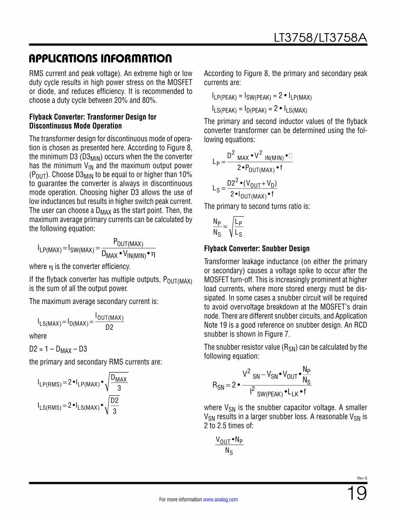
Flyback Converter: Transformer Design for Discontinuous Mode Operation
The transformer design for discontinuous mode of opera-tion is chosen as presented here. According to Figure 8, the minimum D3 (D3MIN) occurs when the the converter has the minimum VIN and the maximum output power (POUT). Choose D3MIN to be equal to or higher than 10% to guarantee the converter is always in discontinuous mode operation. Choosing higher D3 allows the use of low inductances but results in higher switch peak current. The user can choose a DMAX as the start point. Then, the maximum average primary currents can be calculated by the following equation:
ILP(MAX)= ISW(MAX)=
POUT(MAX)
DMAX • VIN(MIN) •η
where h is the converter efficiency.
If the flyback converter has multiple outputs, POUT(MAX) is the sum of all the output power.
The maximum average secondary current is:
ILS(MAX)= ID(MAX) =
IOUT(MAX)
D2where
D2 = 1 – DMAX – D3
the primary and secondary RMS currents are:
ILP(RMS) = 2 •ILP(MAX) •DMAX
3
ILS(RMS) = 2 •ILS(MAX) •D23
According to Figure 8, the primary and secondary peak currents are:
ILP(PEAK) = ISW(PEAK) = 2 • ILP(MAX)
ILS(PEAK) = ID(PEAK) = 2 • ILS(MAX)
The primary and second inductor values of the flyback converter transformer can be determined using the fol-lowing equations:
LP =D2
MAX • V2IN(MIN) • �
2 •POUT(MAX) • f
LS =D22 •(VOUT + VD)2 •IOUT(MAX) • f
The primary to second turns ratio is:
NPNS
=LPLS
Flyback Converter: Snubber Design
Transformer leakage inductance (on either the primary or secondary) causes a voltage spike to occur after the MOSFET turn-off. This is increasingly prominent at higher load currents, where more stored energy must be dis-sipated. In some cases a snubber circuit will be required to avoid overvoltage breakdown at the MOSFET’s drain node. There are different snubber circuits, and Application Note 19 is a good reference on snubber design. An RCD snubber is shown in Figure 7.
The snubber resistor value (RSN) can be calculated by the following equation:
RSN = 2 •
V2 SN −VSN • VOUT •NPNS
I2 SW(PEAK) •LLK • f
where VSN is the snubber capacitor voltage. A smaller VSN results in a larger snubber loss. A reasonable VSN is 2 to 2.5 times of:
VOUT •NPNS
LT3758/LT3758A
20Rev G
For more information www.analog.com
APPLICATIONS INFORMATIONLLK is the leakage inductance of the primary winding, which is usually specified in the transformer character-istics. LLK can be obtained by measuring the primary inductance with the secondary windings shorted. The snubber capacitor value (CCN) can be determined using the following equation:
CCN =
VSNΔVSN •RCN • f
where ∆VSN is the voltage ripple across CCN. A reasonable ∆VSN is 5% to 10% of VSN. The reverse voltage rating of DSN should be higher than the sum of VSN and VIN(MAX).
Flyback Converter: Sense Resistor Selection
In a flyback converter, when the power switch is turned on, the current flowing through the sense resistor (ISENSE) is:
ISENSE = ILP
Set the sense voltage at ILP(PEAK) to be the minimum of the SENSE current limit threshold with a 20% margin. The sense resistor value can then be calculated to be:
RSENSE =
80mVILP(PEAK)
Flyback Converter: Power MOSFET Selection
For the flyback configuration, the MOSFET is selected with a VDC rating high enough to handle the maximum VIN, the reflected secondary voltage and the voltage spike due to the leakage inductance. Approximate the required MOSFET VDC rating using:
BVDSS > VDS(PEAK)
where
VDS(PEAK) = VIN(MAX) + VSN
The power dissipated by the MOSFET in a flyback con-verter is:
PFET = I2M(RMS) • RDS(ON) + 2 • V2DS(PEAK) • IL(MAX) •
CRSS • f/1A
The first term in this equation represents the conduction losses in the device, and the second term, the switching loss. CRSS is the reverse transfer capacitance, which is usually specified in the MOSFET characteristics.
From a known power dissipated in the power MOSFET, its junction temperature can be obtained using the following equation:
TJ = TA + PFET • θJA = TA + PFET • (θJC + θCA)
TJ must not exceed the MOSFET maximum junction temperature rating. It is recommended to measure the MOSFET temperature in steady state to ensure that abso-lute maximum ratings are not exceeded.
Flyback Converter: Output Diode Selection
The output diode in a flyback converter is subject to large RMS current and peak reverse voltage stresses. A fast switching diode with a low forward drop and a low reverse leakage is desired. Schottky diodes are recommended if the output voltage is below 100V.
Approximate the required peak repetitive reverse voltage rating VRRM using:
VRRM >
NSNP
• VIN(MAX)+ VOUT
The power dissipated by the diode is:
PD = IO(MAX) • VD
and the diode junction temperature is:
TJ = TA + PD • RθJA
The RθJA to be used in this equation normally includes the RθJC for the device, plus the thermal resistance from the board to the ambient temperature in the enclosure. TJ must not exceed the diode maximum junction temperature rating.
Flyback Converter: Output Capacitor Selection
The output capacitor of the flyback converter has a similar operation condition as that of the boost converter. Refer to the Boost Converter: Output Capacitor Selection section for the calculation of COUT and ESRCOUT.
The RMS ripple current rating of the output capacitors in discontinuous operation can be determined using the following equation:
IRMS(COUT),DISCONTINUOUS ≥ IO(MAX) •
4−(3•D2)3•D2
LT3758/LT3758A
21Rev G
For more information www.analog.com
APPLICATIONS INFORMATIONFlyback Converter: Input Capacitor Selection
The input capacitor in a flyback converter is subject to a large RMS current due to the discontinuous primary current. To prevent large voltage transients, use a low ESR input capacitor sized for the maximum RMS current. The RMS ripple current rating of the input capacitors in discontinuous operation can be determined using the fol-lowing equation:
IRMS(CIN),DISCONTINUOUS ≥POUT(MAX)
VIN(MIN) •η•
4−(3•DMAX)3•DMAX
SEPIC CONVERTER APPLICATIONS
The LT3758 can be configured as a SEPIC (single-ended primary inductance converter), as shown in Figure 1. This topology allows for the input to be higher, equal, or lower than the desired output voltage. The conversion ratio as a function of duty cycle is:
VOUT+VD
VIN= D1−D
in continuous conduction mode (CCM).
In a SEPIC converter, no DC path exists between the input and output. This is an advantage over the boost converter for applications requiring the output to be disconnected from the input source when the circuit is in shutdown.
Compared to the flyback converter, the SEPIC converter has the advantage that both the power MOSFET and the output diode voltages are clamped by the capacitors (CIN, CDC and COUT), therefore, there is less voltage ringing across the power MOSFET and the output diodes. The SEPIC converter requires much smaller input capacitors than those of the flyback converter. This is due to the fact that, in the SEPIC converter, the inductor L1 is in series with the input, and the ripple current flowing through the input capacitor is continuous.
SEPIC Converter: Switch Duty Cycle and Frequency
For a SEPIC converter operating in CCM, the duty cycle of the main switch can be calculated based on the output voltage (VOUT), the input voltage (VIN) and the diode for-ward voltage (VD).
The maximum duty cycle (DMAX) occurs when the con-verter has the minimum input voltage:
DMAX =
VOUT + VDVIN(MIN)+ VOUT + VD
SEPIC Converter: Inductor and Sense Resistor Selection
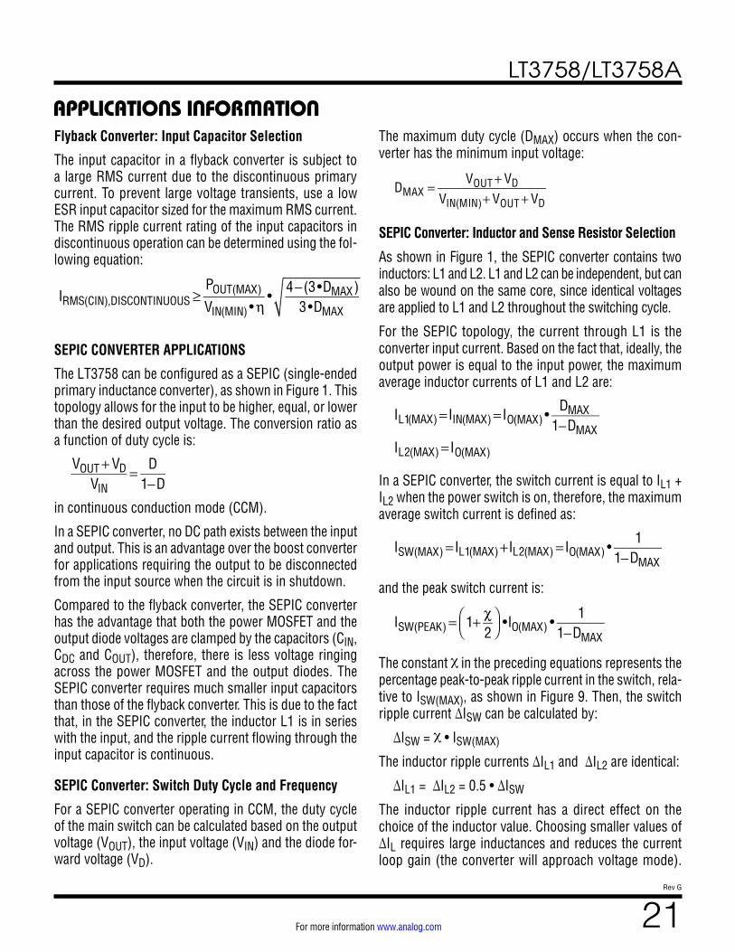
As shown in Figure 1, the SEPIC converter contains two inductors: L1 and L2. L1 and L2 can be independent, but can also be wound on the same core, since identical voltages are applied to L1 and L2 throughout the switching cycle.
For the SEPIC topology, the current through L1 is the converter input current. Based on the fact that, ideally, the output power is equal to the input power, the maximum average inductor currents of L1 and L2 are:
IL1(MAX)= IIN(MAX)= IO(MAX) •DMAX
1−DMAX
IL2(MAX)= IO(MAX)
In a SEPIC converter, the switch current is equal to IL1 + IL2 when the power switch is on, therefore, the maximum average switch current is defined as:
ISW(MAX)= IL1(MAX)+IL2(MAX)= IO(MAX) •
11−DMAX
and the peak switch current is:
ISW(PEAK)= 1+ χ
2⎛⎝⎜
⎞⎠⎟ •IO(MAX) •
11−DMAX
The constant c in the preceding equations represents the percentage peak-to-peak ripple current in the switch, rela-tive to ISW(MAX), as shown in Figure 9. Then, the switch ripple current ∆ISW can be calculated by:
∆ISW = c • ISW(MAX)
The inductor ripple currents ∆IL1 and ∆IL2 are identical:
∆IL1 = ∆IL2 = 0.5 • ∆ISW
The inductor ripple current has a direct effect on the choice of the inductor value. Choosing smaller values of ∆IL requires large inductances and reduces the current loop gain (the converter will approach voltage mode).
LT3758/LT3758A
22Rev G
For more information www.analog.com
APPLICATIONS INFORMATIONAccepting larger values of ∆IL allows the use of low induc-tances, but results in higher input current ripple, greater core losses, and in some cases, subharmonic oscillation. A good starting point for c is 0.2 and careful evaluation of system stability should be made to ensure adequate design margin.
Figure 9. The Switch Current Waveform of the SEPIC Converter
3758 F09
∆ISW = χ • ISW(MAX)
ISW
tDTS
ISW(MAX)
TS
where
χL1=ΔIL1
IL1(MAX)
IL2(RMS)= IL2(MAX) • 1+ χ2 L212
where
χL2 =
ΔIL2IL2 (MAX)
Based on the preceding equations, the user should choose the inductors having sufficient saturation and RMS cur-rent ratings.
In a SEPIC converter, when the power switch is turned on, the current flowing through the sense resistor (ISENSE) is the switch current.
Set the sense voltage at ISENSE(PEAK) to be the minimum of the SENSE current limit threshold with a 20% margin. The sense resistor value can then be calculated to be:
RSENSE =
80 mVISW(PEAK)
SEPIC Converter: Power MOSFET Selection
For the SEPIC configuration, choose a MOSFET with a VDC rating higher than the sum of the output voltage and input voltage by a safety margin (a 10V safety margin is usually sufficient).
The power dissipated by the MOSFET in a SEPIC con-verter is:
PFET = I2SW(MAX) • RDS(ON) • DMAX
+ 2 • (VIN(MIN) + VOUT)2 • IL(MAX) • CRSS • f/1A
The first term in this equation represents the conduction losses in the device, and the second term, the switching loss. CRSS is the reverse transfer capacitance, which is usually specified in the MOSFET characteristics.
For maximum efficiency, RDS(ON) and CRSS should be minimized. From a known power dissipated in the power
Given an operating input voltage range, and having cho-sen the operating frequency and ripple current in the inductor, the inductor value (L1 and L2 are independent) of the SEPIC converter can be determined using the fol-lowing equation:
L1=L2=
VIN(MIN)
0.5•ΔISW • f•DMAX
For most SEPIC applications, the equal inductor values will fall in the range of 1µH to 100µH.
By making L1 = L2, and winding them on the same core, the value of inductance in the preceding equation is replaced by 2L, due to mutual inductance:
L =
VIN(MIN)
ΔISW • f•DMAX
This maintains the same ripple current and energy storage in the inductors. The peak inductor currents are:
IL1(PEAK) = IL1(MAX) + 0.5 • ∆IL1
IL2(PEAK) = IL2(MAX) + 0.5 • ∆IL2
The RMS inductor currents are:
IL1(RMS)= IL1(MAX) • 1+ χ2 L112
LT3758/LT3758A
23Rev G
For more information www.analog.com
APPLICATIONS INFORMATIONMOSFET, its junction temperature can be obtained using the following equation:
TJ = TA + PFET • θJA = TA + PFET • (θJC + θCA)
TJ must not exceed the MOSFET maximum junction temperature rating. It is recommended to measure the MOSFET temperature in steady state to ensure that abso-lute maximum ratings are not exceeded.
SEPIC Converter: Output Diode Selection
To maximize efficiency, a fast switching diode with a low forward drop and low reverse leakage is desirable. The average forward current in normal operation is equal to the output current, and the peak current is equal to:
ID(PEAK)= 1+ χ
2⎛⎝⎜
⎞⎠⎟ •IO(MAX) •
11−DMAX
It is recommended that the peak repetitive reverse voltage rating VRRM is higher than VOUT + VIN(MAX) by a safety margin (a 10V safety margin is usually sufficient).
The power dissipated by the diode is:
PD = IO(MAX) • VD
and the diode junction temperature is:
TJ = TA + PD • RθJA
The RθJA used in this equation normally includes the RθJC for the device, plus the thermal resistance from the board, to the ambient temperature in the enclosure. TJ must not exceed the diode maximum junction temperature rating.
SEPIC Converter: Output and Input Capacitor Selection
The selections of the output and input capacitors of the SEPIC converter are similar to those of the boost converter. Please refer to the Boost Converter: Output Capacitor Selection and Boost Converter: Input Capacitor Selection sections.
SEPIC Converter: Selecting the DC Coupling Capacitor
The DC voltage rating of the DC coupling capacitor (CDC, as shown in Figure 1) should be larger than the maximum input voltage:
VCDC > VIN(MAX)
CDC has nearly a rectangular current waveform. During the switch off-time, the current through CDC is IIN, while approximately –IO flows during the on-time. The RMS rating of the coupling capacitor is determined by the fol-lowing equation:
IRMS(CDC) > IO(MAX) •VOUT + VDVIN(MIN)
A low ESR and ESL, X5R or X7R ceramic capacitor works well for CDC.
INVERTING CONVERTER APPLICATIONS
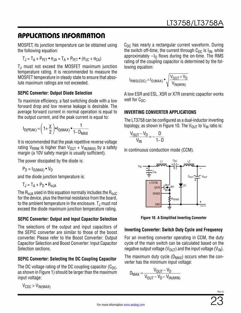
The LT3758 can be configured as a dual-inductor inverting topology, as shown in Figure 10. The VOUT to VIN ratio is:
VOUT−VDVIN
= − D1−D
in continuous conduction mode (CCM).
Figure 10. A Simplified Inverting Converter
RSENSE
CDC
VIN
CIN
L1
D1
COUT VOUT
3758 F10
+
GATE
GND
LT3758
SENSE
L2
M1
+
–+ –
+
Inverting Converter: Switch Duty Cycle and Frequency
For an inverting converter operating in CCM, the duty cycle of the main switch can be calculated based on the negative output voltage (VOUT) and the input voltage (VIN).
The maximum duty cycle (DMAX) occurs when the con-verter has the minimum input voltage:
DMAX =
VOUT−VDVOUT−VD−VIN(MIN)
LT3758/LT3758A
24Rev G
For more information www.analog.com
Inverting Converter: Inductor, Sense Resistor, Power MOSFET, Output Diode and Input Capacitor Selections
The selections of the inductor, sense resistor, power MOSFET, output diode and input capacitor of an invert-ing converter are similar to those of the SEPIC converter. Please refer to the corresponding SEPIC converter sections.
Inverting Converter: Output Capacitor Selection
The inverting converter requires much smaller output capacitors than those of the boost, flyback and SEPIC converters for similar output ripples. This is due to the fact that, in the inverting converter, the inductor L2 is in series with the output, and the ripple current flowing through the output capacitors are continuous. The output ripple voltage is produced by the ripple current of L2 flow-ing through the ESR and bulk capacitance of the output capacitor:
ΔVOUT(P–P)= ΔIL2 • ESRCOUT +
18 • f •COUT
⎛⎝⎜
⎞⎠⎟
After specifying the maximum output ripple, the user can select the output capacitors according to the preceding equation.
The ESR can be minimized by using high quality X5R or X7R dielectric ceramic capacitors. In many applications, ceramic capacitors are sufficient to limit the output volt-age ripple.
The RMS ripple current rating of the output capacitor needs to be greater than:
IRMS(COUT) > 0.3 • ∆IL2
Inverting Converter: Selecting the DC Coupling Capacitor
The DC voltage rating of the DC coupling capacitor (CDC, as shown in Figure 10) should be larger than the maxi-mum input voltage minus the output voltage (negative voltage):
VCDC > VIN(MAX) – VOUT
CDC has nearly a rectangular current waveform. During the switch off-time, the current through CDC is IIN, while approximately –IO flows during the on-time. The RMS rating of the coupling capacitor is determined by the fol-lowing equation:
IRMS(CDC)>IO(MAX) •
DMAX1−DMAX
A low ESR and ESL, X5R or X7R ceramic capacitor works well for CDC.
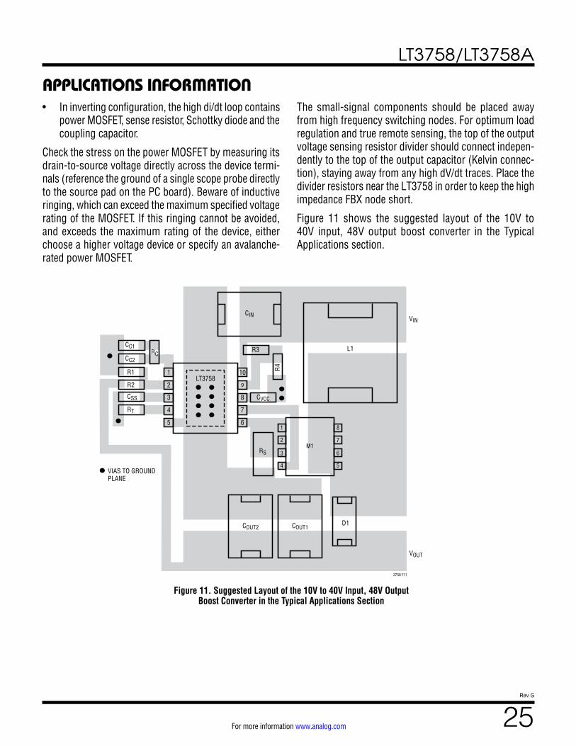
Board Layout
The high speed operation of the LT3758 demands careful attention to board layout and component placement. The Exposed Pad of the package is the only GND terminal of the IC, and is important for thermal management of the IC. Therefore, it is crucial to achieve a good electrical and thermal contact between the Exposed Pad and the ground plane of the board. For the LT3758 to deliver its full output power, it is imperative that a good thermal path be pro-vided to dissipate the heat generated within the package. It is recommended that multiple vias in the printed circuit board be used to conduct heat away from the IC and into a copper plane with as much area as possible.
To prevent radiation and high frequency resonance prob-lems, proper layout of the components connected to the IC is essential, especially the power paths with higher di/dt. The following high di/dt loops of different topologies should be kept as tight as possible to reduce inductive ringing:
• In boost configuration, the high di/dt loop contains the output capacitor, the sensing resistor, the power MOSFET and the Schottky diode.
• In flyback configuration, the high di/dt primary loop contains the input capacitor, the primary winding, the power MOSFET and the sensing resistor. The high di/dt secondary loop contains the output capacitor, the secondary winding and the output diode.
• In SEPIC configuration, the high di/dt loop contains the power MOSFET, sense resistor, output capacitor, Schottky diode and the coupling capacitor.
APPLICATIONS INFORMATION
LT3758/LT3758A
25Rev G
For more information www.analog.com
APPLICATIONS INFORMATION• In inverting configuration, the high di/dt loop contains
power MOSFET, sense resistor, Schottky diode and the coupling capacitor.
Check the stress on the power MOSFET by measuring its drain-to-source voltage directly across the device termi-nals (reference the ground of a single scope probe directly to the source pad on the PC board). Beware of inductive ringing, which can exceed the maximum specified voltage rating of the MOSFET. If this ringing cannot be avoided, and exceeds the maximum rating of the device, either choose a higher voltage device or specify an avalanche-rated power MOSFET.
The small-signal components should be placed away from high frequency switching nodes. For optimum load regulation and true remote sensing, the top of the output voltage sensing resistor divider should connect indepen-dently to the top of the output capacitor (Kelvin connec-tion), staying away from any high dV/dt traces. Place the divider resistors near the LT3758 in order to keep the high impedance FBX node short.
Figure 11 shows the suggested layout of the 10V to 40V input, 48V output boost converter in the Typical Applications section.
Figure 11. Suggested Layout of the 10V to 40V Input, 48V Output Boost Converter in the Typical Applications Section
VIN
3758 F11
VOUT
L1
VIAS TO GROUND PLANE
D1COUT1COUT2
1
2
8
7
3
4
6
5
M1
CIN
RC
R1
R2
CSS
RT
R3
R4
CVCC
CC1
CC2
LT37581
2
3
4
5
9
10
6
7
8
RS
LT3758/LT3758A
26Rev G
For more information www.analog.com
APPLICATIONS INFORMATION
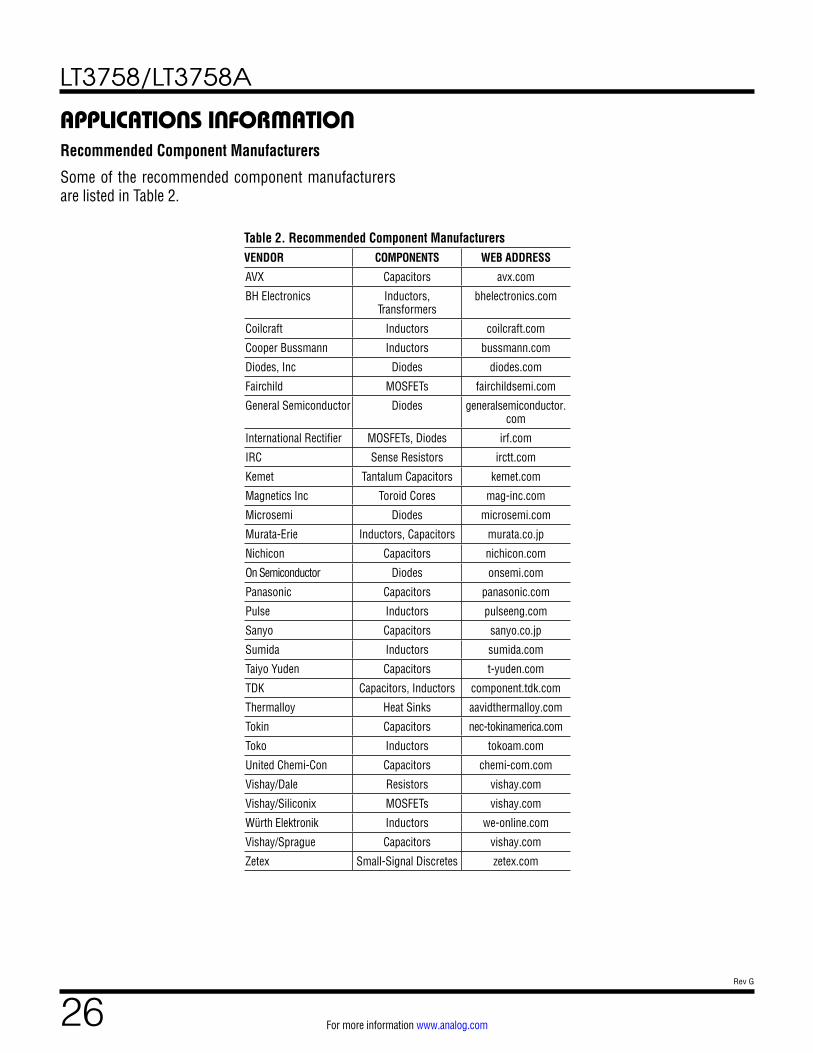
Table 2. Recommended Component ManufacturersVENDOR COMPONENTS WEB ADDRESS
AVX Capacitors avx.com
BH Electronics Inductors, Transformers
bhelectronics.com
Coilcraft Inductors coilcraft.com
Cooper Bussmann Inductors bussmann.com
Diodes, Inc Diodes diodes.com
Fairchild MOSFETs fairchildsemi.com
General Semiconductor Diodes generalsemiconductor.com
International Rectifier MOSFETs, Diodes irf.com
IRC Sense Resistors irctt.com
Kemet Tantalum Capacitors kemet.com
Magnetics Inc Toroid Cores mag-inc.com
Microsemi Diodes microsemi.com
Murata-Erie Inductors, Capacitors murata.co.jp
Nichicon Capacitors nichicon.com
On Semiconductor Diodes onsemi.com
Panasonic Capacitors panasonic.com
Pulse Inductors pulseeng.com
Sanyo Capacitors sanyo.co.jp
Sumida Inductors sumida.com
Taiyo Yuden Capacitors t-yuden.com
TDK Capacitors, Inductors component.tdk.com
Thermalloy Heat Sinks aavidthermalloy.com
Tokin Capacitors nec-tokinamerica.com
Toko Inductors tokoam.com
United Chemi-Con Capacitors chemi-com.com
Vishay/Dale Resistors vishay.com
Vishay/Siliconix MOSFETs vishay.com
Würth Elektronik Inductors we-online.com
Vishay/Sprague Capacitors vishay.com
Zetex Small-Signal Discretes zetex.com
Recommended Component Manufacturers
Some of the recommended component manufacturers are listed in Table 2.
LT3758/LT3758A
27Rev G
For more information www.analog.com
TYPICAL APPLICATIONS
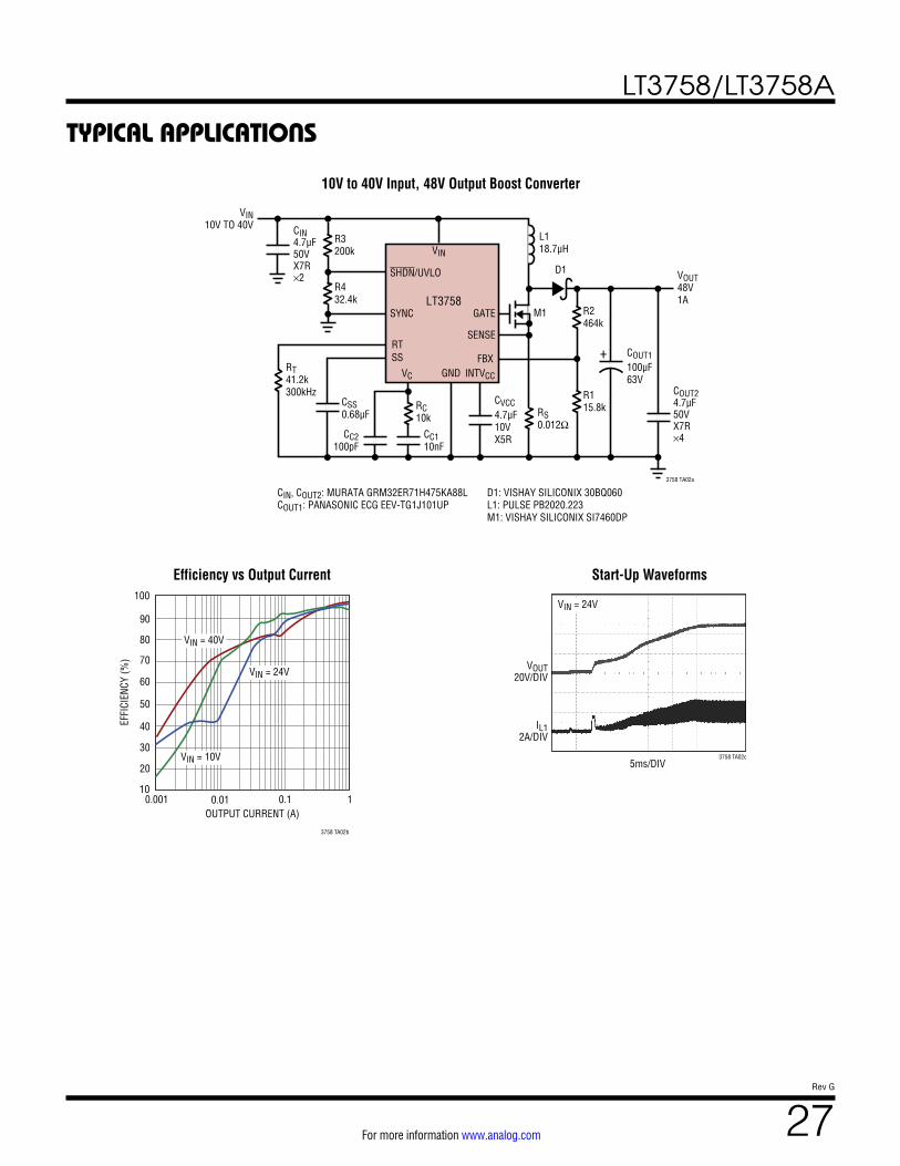
10V to 40V Input, 48V Output Boost Converter
Efficiency vs Output Current
SENSE
LT3758
VIN
VIN10V TO 40V CIN
4.7µF50VX7R×2 VOUT
48V1A
RS0.012Ω
RT41.2k300kHz
GATE
FBXGND INTVCC
SHDN/UVLO
SYNC
RTSS
R3200k
R432.4k
CSS0.68µF
CC2100pF
RC10k
CC110nF
L118.7µH
3758 TA02a
R2464k
D1
M1
R115.8k
CVCC4.7µF10VX5R
COUT24.7µF50V X7R×4
COUT1100µF63V
+
CIN, COUT2: MURATA GRM32ER71H475KA88LCOUT1: PANASONIC ECG EEV-TG1J101UP
D1: VISHAY SILICONIX 30BQ060L1: PULSE PB2020.223M1: VISHAY SILICONIX SI7460DP
VC
OUTPUT CURRENT (A)0.001
EFFI
CIEN
CY (%
)
10
50
40
30
20
60
70
80
90
100
0.01 0.1
3758 TA02b
1
VIN = 40V
VIN = 24V
VIN = 10V
Start-Up Waveforms
5ms/DIV
VOUT20V/DIV
IL12A/DIV
3758 TA02c
VIN = 24V
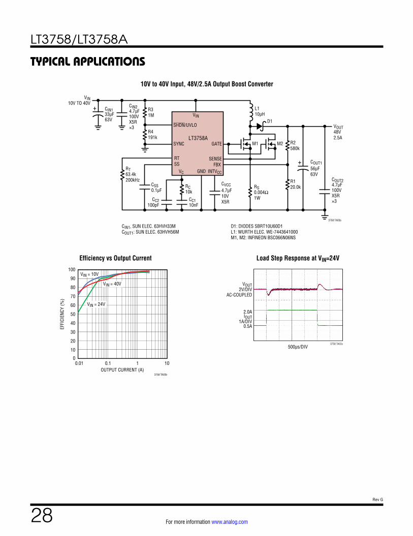
LT3758/LT3758A
28Rev G
For more information www.analog.com
TYPICAL APPLICATIONS
10V to 40V Input, 48V/2.5A Output Boost Converter
Load Step Response at VIN=24VEfficiency vs Output Current
SENSE
LT3758A
VIN
VIN10V TO 40V CIN2
4.7µF100VX5R×3
CIN133µF63V
VOUT48V2.5A
RS0.004Ω1W
RT63.4k200kHz
GATE
FBXGND INTVCC
SHDN/UVLO
SYNC
RTSS
R31M
R4191k
CSS0.1µF
CC2100pF
RC10k
CC110nF
L110µH
3758 TA03a
R2580k
D1
M1 M2
R120.0k
CVCC4.7µF10VX5R
COUT24.7µF100V X5R×3
COUT156µF63V
+
CIN1, SUN ELEC. 63HVH33MCOUT1: SUN ELEC. 63HVH56M
D1: DIODES SBRT10U60D1L1: WURTH ELEC. WE-7443641000M1, M2: INFINEON BSC066N06NS
VC
+
500µs/DIV
VOUT2V/DIV
AC-COUPLED
IOUT1A/DIV
0.5A
2.0A
3758 TA03c
VIN = 10V
VIN = 40V
VIN = 24V
OUTPUT CURRENT (A)0.01
EFFI
CIEN
CY (%
)
100
10
90
70
50
30
80
60
40
20
00.1 1
3758 TA03b
10
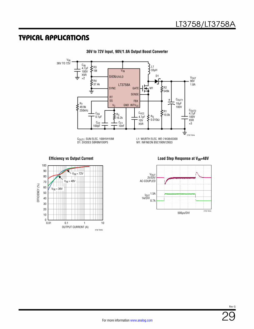
LT3758/LT3758A
29Rev G
For more information www.analog.com
TYPICAL APPLICATIONS
36V to 72V Input, 90V/1.8A Output Boost Converter
Load Step Response at VIN=48VEfficiency vs Output Current
SENSE
LT3758A
VIN
VIN36V TO 72V CIN
4.7µF100VX5R×2 VOUT
90V1.8A
RS0.010Ω
RT49.9k250kHz
GATE
FBXGND INTVCC
SHDN/UVLO
SYNC
RTSS
R31M
R437.4k
CSS0.1µF
CC2100pF
RC16.2k
CC110nF
L133µH
3758 TA04a
R2549k
D1
M1
R110.0k
CVCC4.7µF10VX5R
COUT24.7µF100V X5R×3
COUT110µF100V
+
COUT1: SUN ELEC. 100HVH10MD1: DIODES SBR8M100P5
L1: WURTH ELEC. WE-7443643300M1: INFINEON BSC190N12NS3
VC
500µs/DIV
VOUT2V/DIV
AC-COUPLED
IOUT1A/DIV
0.7A
1.5A
3758 TA04c
VIN = 72V
VIN = 48V
VIN = 36V
OUTPUT CURRENT (A)0.01
EFFI
CIEN
CY (%
)
100
10
90
70
50
30
80
60
40
20
00.1 1
3758 TA04b
10
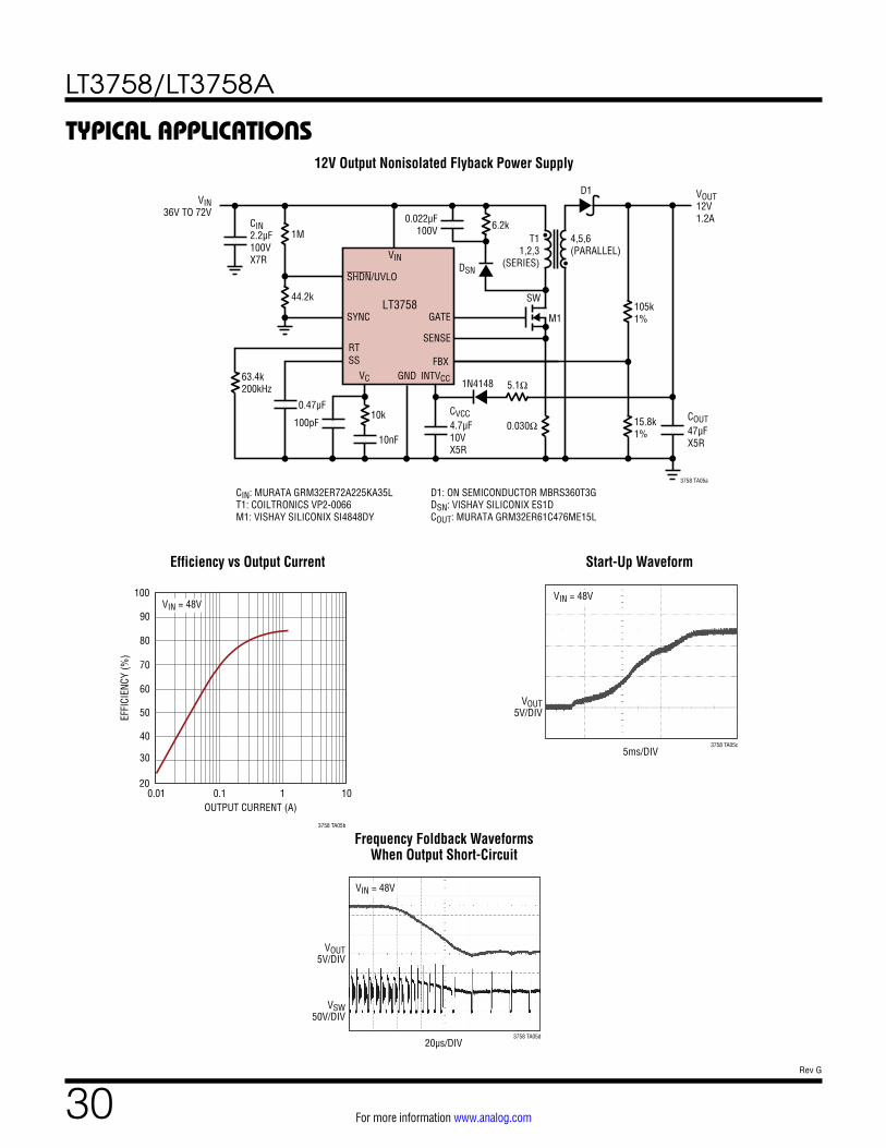
LT3758/LT3758A
30Rev G
For more information www.analog.com
TYPICAL APPLICATIONS12V Output Nonisolated Flyback Power Supply
Efficiency vs Output Current Start-Up Waveform
SENSE
LT3758
VINDSN
VIN36V TO 72V
CIN2.2µF100VX7R
63.4k200kHz
GATE
FBXGND INTVCC
SHDN/UVLO
SYNC
RTSS
0.022µF100V
T11,2,3
(SERIES)
4,5,6(PARALLEL)
1M
44.2k
0.47µF
100pF10k
10nF0.030Ω
5.1Ω1N4148
15.8k1%
105k1%
CVCC4.7µF10VX5R
VOUT12V1.2A
3758 TA05a
COUT47µFX5R
6.2k
D1
SW
M1
CIN: MURATA GRM32ER72A225KA35LT1: COILTRONICS VP2-0066M1: VISHAY SILICONIX SI4848DY
D1: ON SEMICONDUCTOR MBRS360T3GDSN: VISHAY SILICONIX ES1DCOUT: MURATA GRM32ER61C476ME15L
VC
OUTPUT CURRENT (A)0.01
EFFI
CIEN
CY (%
)
20
50
40
30
60
70
80
90
100
0.1 1
3758 TA05b
10
VIN = 48V
5ms/DIV
VOUT5V/DIV
3758 TA05c
VIN = 48V
Frequency Foldback WaveformsWhen Output Short-Circuit
20µs/DIV
VOUT5V/DIV
VSW50V/DIV
3758 TA05d
VIN = 48V
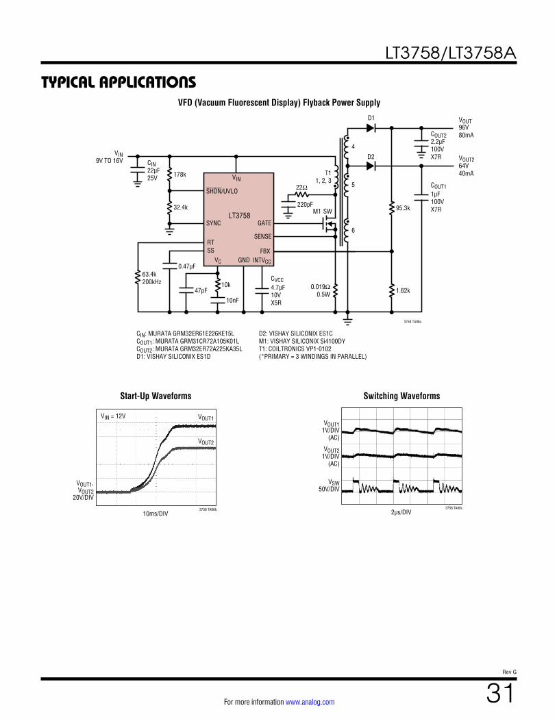
LT3758/LT3758A
31Rev G
For more information www.analog.com
10ms/DIV
VOUT1,VOUT2
20V/DIV
3758 TA06b
VIN = 12V VOUT1
VOUT2
2µs/DIV
VSW50V/DIV
VOUT21V/DIV
(AC)
VOUT11V/DIV
(AC)
3758 TA06c
TYPICAL APPLICATIONSVFD (Vacuum Fluorescent Display) Flyback Power Supply
Start-Up Waveforms Switching Waveforms
SENSE
LT3758
VIN
VIN9V TO 16V CIN
22µF25V
63.4k200kHz
GATE
FBXGND INTVCC
SHDN/UVLO
SYNC
RTSS
COUT22.2µF100VX7R
T11, 2, 3
4
5
6
178k
32.4k
0.47µF
47pF10k
10nF
0.019Ω0.5W 1.62k
95.3k
D1
D2
CVCC4.7µF10VX5R
VOUT96V80mA
VOUT264V40mA
3758 TA06a
COUT11µF100VX7RSWM1
CIN: MURATA GRM32ER61E226KE15LCOUT1: MURATA GRM31CR72A105K01LCOUT2: MURATA GRM32ER72A225KA35LD1: VISHAY SILICONIX ES1D
D2: VISHAY SILICONIX ES1CM1: VISHAY SILICONIX Si4100DYT1: COILTRONICS VP1-0102 (*PRIMARY = 3 WINDINGS IN PARALLEL)
220pF
22Ω
VC
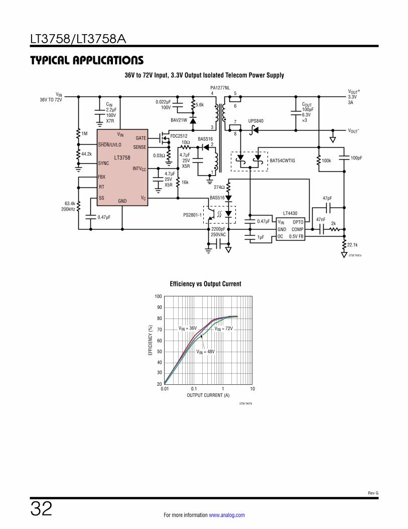
LT3758/LT3758A
32Rev G
For more information www.analog.com
TYPICAL APPLICATIONS36V to 72V Input, 3.3V Output Isolated Telecom Power Supply
SENSE
LT3758
VIN
INTVCC
BAV21W
FDC2512
0.03Ω
VIN36V TO 72V
CIN2.2µF100VX7R
63.4k200kHz
GATE
FBX
GND
SHDN/UVLO
SYNC
RT
SS
0.022µF100V
4.7µF25VX5R
1M
44.2k
0.47µF
VOUT+3.3V3A
VOUT-
3758 TA07a
5.6k
16k
4.7µF25VX5R
10Ω
274Ω
BAS516
PS2801-1
BAS5162
4
38
7
6
UPS840
5
1
0.47µF
LT443047nF
1µF
VIN
GNDOPTOCOMP
OC 0.5V FB
47pF
2k
22.1k
100kBAT54CWTIG
2200pF250VAC
100pF
COUT100µF6.3V×3
PA1277NL
VC
OUTPUT CURRENT (A)0.01
EFFI
CIEN
CY (%
)
20
50
40
30
60
70
80
90
100
0.1 1
3758 TA07b
10
VIN = 36V VIN = 72V
VIN = 48V
Efficiency vs Output Current
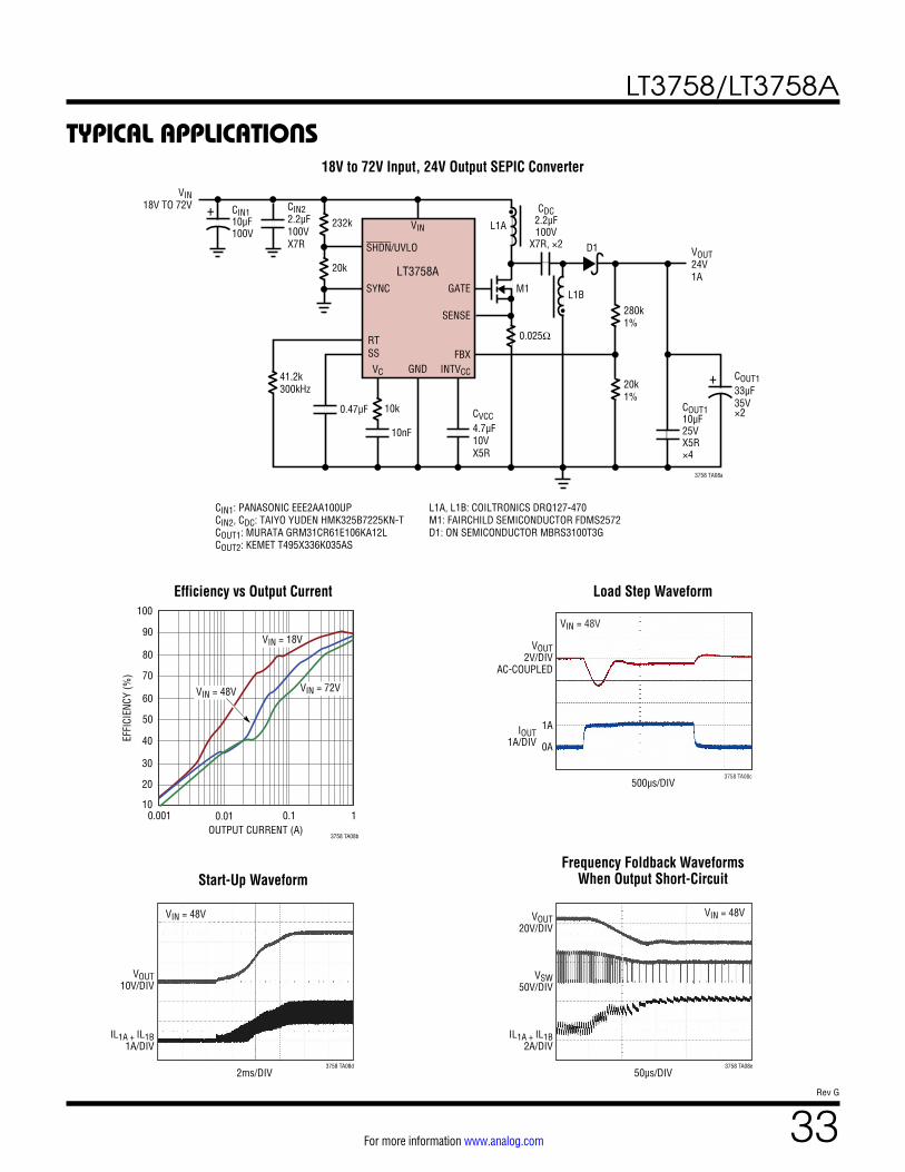
LT3758/LT3758A
33Rev G
For more information www.analog.com
TYPICAL APPLICATIONS18V to 72V Input, 24V Output SEPIC Converter
SENSE
LT3758A
VIN
VIN18V TO 72V CIN2
2.2µF100VX7R
CDC2.2µF100V
X7R, ×2VOUT24V1A
0.025Ω
M1
41.2k300kHz
GATE
FBXGND INTVCC
SHDN/UVLO
SYNC
RTSS
•
•232k
20k
0.47µF
10nF
10k
L1A
L1B
D1
CIN1: PANASONIC EEE2AA100UPCIN2, CDC: TAIYO YUDEN HMK325B7225KN-TCOUT1: MURATA GRM31CR61E106KA12LCOUT2: KEMET T495X336K035AS
3758 TA08a
280k1%
20k1%
COUT110µF25VX5R×4
CVCC4.7µF10VX5R
L1A, L1B: COILTRONICS DRQ127-470M1: FAIRCHILD SEMICONDUCTOR FDMS2572D1: ON SEMICONDUCTOR MBRS3100T3G
VC
CIN110µF100V
COUT133µF35V×2
+
+
Efficiency vs Output Current
OUTPUT CURRENT (A)0.001
10
EFFI
CIEN
CY (%
)
30
20
40
50
60
70
80
90
100
0.01 0.1
3758 TA08b
1
VIN = 72VVIN = 48V
VIN = 18V
Load Step Waveform
500µs/DIV
VOUT2V/DIV
AC-COUPLED
IOUT1A/DIV 0A
1A
3758 TA08c
VIN = 48V
Start-Up Waveform
2ms/DIV
VOUT10V/DIV
IL1A + IL1B1A/DIV
3758 TA08d
VIN = 48V
50µs/DIV
VSW50V/DIV
VOUT20V/DIV
IL1A + IL1B2A/DIV
3758 TA08e
VIN = 48V
Frequency Foldback WaveformsWhen Output Short-Circuit
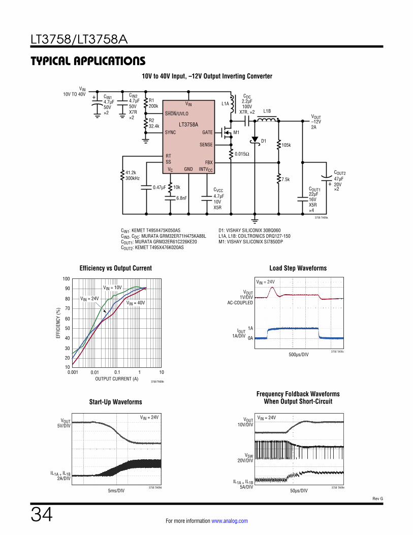
LT3758/LT3758A
34Rev G
For more information www.analog.com
TYPICAL APPLICATIONS10V to 40V Input, –12V Output Inverting Converter
SENSE
LT3758A
VIN
VIN10V TO 40V CIN2
4.7µF50VX7R×2
CDC2.2µF100V
X7R, ×2
0.015Ω
M1
41.2k300kHz
GATE
FBXGND INTVCC
SHDN/UVLO
SYNC
RTSS
•
0.47µF 10k
L1A
3758 TA09a
CVCC4.7µF10VX5R
VC
CIN14.7µF50V×2
COUT247µF20V×2
+
+ R1200k
R232.4k
6.8nF
•L1B
D1
VOUT–12V2A
105k
7.5k
COUT122µF16VX5R×4
CIN1: KEMET T495X475K050ASCIN2, CDC: MURATA GRM32ER71H475KA88LCOUT1: MURATA GRM32ER61C226KE20COUT2: KEMET T495X476K020AS
D1: VISHAY SILICONIX 30BQ060L1A, L1B: COILTRONICS DRQ127-150M1: VISHAY SILICONIX SI7850DP
Efficiency vs Output Current
OUTPUT CURRENT (A)0.001
10
EFFI
CIEN
CY (%
)
30
20
40
50
60
70
80
90
100
0.01 0.1 1
3758 TA09b
10
VIN = 40VVIN = 24V
VIN = 10V
Load Step Waveforms
Start-Up Waveforms
5ms/DIV
VOUT5V/DIV
IL1A + IL1B2A/DIV
3758 TA09d
VIN = 24V
50µs/DIV
VSW20V/DIV
VOUT10V/DIV
IL1A + IL1B5A/DIV 3758 TA09e
VIN = 24V
Frequency Foldback WaveformsWhen Output Short-Circuit
500µs/DIV
VOUT1V/DIV
AC-COUPLED
IOUT1A/DIV 0A
1A
3758 TA09c
VIN = 24V
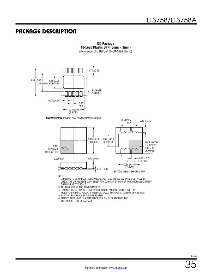
LT3758/LT3758A
35Rev G
For more information www.analog.com
PACKAGE DESCRIPTION
3.00 ±0.10(4 SIDES)
NOTE:1. DRAWING TO BE MADE A JEDEC PACKAGE OUTLINE M0-229 VARIATION OF (WEED-2). CHECK THE LTC WEBSITE DATA SHEET FOR CURRENT STATUS OF VARIATION ASSIGNMENT2. DRAWING NOT TO SCALE3. ALL DIMENSIONS ARE IN MILLIMETERS4. DIMENSIONS OF EXPOSED PAD ON BOTTOM OF PACKAGE DO NOT INCLUDE MOLD FLASH. MOLD FLASH, IF PRESENT, SHALL NOT EXCEED 0.15mm ON ANY SIDE5. EXPOSED PAD SHALL BE SOLDER PLATED6. SHADED AREA IS ONLY A REFERENCE FOR PIN 1 LOCATION ON THE TOP AND BOTTOM OF PACKAGE
0.40 ± 0.10
BOTTOM VIEW—EXPOSED PAD
1.65 ± 0.10(2 SIDES)
0.75 ±0.05
R = 0.125TYP
2.38 ±0.10(2 SIDES)
15
106
PIN 1TOP MARK
(SEE NOTE 6)
0.200 REF
0.00 – 0.05
(DD) DFN REV C 0310
0.25 ± 0.05
2.38 ±0.05(2 SIDES)
RECOMMENDED SOLDER PAD PITCH AND DIMENSIONS
1.65 ±0.05(2 SIDES)2.15 ±0.05
0.50BSC
0.70 ±0.05
3.55 ±0.05
PACKAGEOUTLINE
0.25 ± 0.050.50 BSC
DD Package10-Lead Plastic DFN (3mm × 3mm)
(Reference LTC DWG # 05-08-1699 Rev C)
PIN 1 NOTCHR = 0.20 OR0.35 × 45°CHAMFER
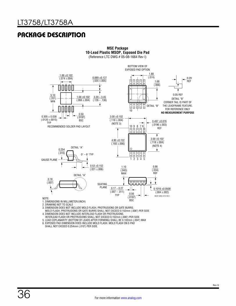
LT3758/LT3758A
36Rev G
For more information www.analog.com
PACKAGE DESCRIPTION
MSOP (MSE) 0213 REV I
0.53 ±0.152(.021 ±.006)
SEATINGPLANE
0.18(.007)
1.10(.043)MAX
0.17 – 0.27(.007 – .011)
TYP
0.86(.034)REF
0.50(.0197)
BSC
1 2 3 4 5
4.90 ±0.152(.193 ±.006)
0.497 ±0.076(.0196 ±.003)
REF8910
10
1
7 6
3.00 ±0.102(.118 ±.004)
(NOTE 3)
3.00 ±0.102(.118 ±.004)
(NOTE 4)
NOTE:1. DIMENSIONS IN MILLIMETER/(INCH)2. DRAWING NOT TO SCALE3. DIMENSION DOES NOT INCLUDE MOLD FLASH, PROTRUSIONS OR GATE BURRS. MOLD FLASH, PROTRUSIONS OR GATE BURRS SHALL NOT EXCEED 0.152mm (.006") PER SIDE4. DIMENSION DOES NOT INCLUDE INTERLEAD FLASH OR PROTRUSIONS. INTERLEAD FLASH OR PROTRUSIONS SHALL NOT EXCEED 0.152mm (.006") PER SIDE5. LEAD COPLANARITY (BOTTOM OF LEADS AFTER FORMING) SHALL BE 0.102mm (.004") MAX6. EXPOSED PAD DIMENSION DOES INCLUDE MOLD FLASH. MOLD FLASH ON E-PAD SHALL NOT EXCEED 0.254mm (.010") PER SIDE.
0.254(.010) 0° – 6° TYP
DETAIL “A”
DETAIL “A”
GAUGE PLANE
5.10(.201)MIN
3.20 – 3.45(.126 – .136)
0.889 ±0.127(.035 ±.005)
RECOMMENDED SOLDER PAD LAYOUT
1.68 ±0.102(.066 ±.004)
1.88 ±0.102(.074 ±.004)
0.50(.0197)
BSC0.305 ± 0.038(.0120 ±.0015)
TYP
BOTTOM VIEW OFEXPOSED PAD OPTION
1.68(.066)
1.88(.074)
0.1016 ±0.0508(.004 ±.002)
DETAIL “B”
DETAIL “B”CORNER TAIL IS PART OF
THE LEADFRAME FEATURE.FOR REFERENCE ONLY
NO MEASUREMENT PURPOSE
0.05 REF
0.29REF
MSE Package10-Lead Plastic MSOP, Exposed Die Pad
(Reference LTC DWG # 05-08-1664 Rev I)
LT3758/LT3758A
37Rev G
For more information www.analog.com
Information furnished by Analog Devices is believed to be accurate and reliable. However, no responsibility is assumed by Analog Devices for its use, nor for any infringements of patents or other rights of third parties that may result from its use. Specifications subject to change without notice. No license is granted by implication or otherwise under any patent or patent rights of Analog Devices.
REVISION HISTORYREV DATE DESCRIPTION PAGE NUMBER
A 3/10 Deleted Bullet from Features and Last Line of DescriptionUpdated All Sections to Include H-Grade and Military GradeDeleted Vendor Telephone Information from Table 2 in Applications Information SectionRevised TA04 and TA04c in Typical ApplicationsReplaced Related Parts List
12 to 7
262936
B 5/10 Revised last sentence of SYNC Pin descriptionUpdated Block DiagramRevised value in last sentence of Programming Turn-on and Turn-off Thresholds in the SHDN/UVLO Pin SectionRevised penultimate sentence of Operating Frequency and Synchronization section
89
1013
C 5/11 Revised MP-grade temperature range in Absolute Maximum Ratings and Order InformationRevised Note 2Revised formula in Applications Information
24
19
D 07/12 Added LT3758A version Throughout
Updated Block Diagram 9
Updated Programming the Output Voltage section 13
Updated Loop Compensation section 14
Updated the schematic and Load Step Waveforms in the Typical Applications section 31, 32
E 6/17 Text Clarification 16, 22
F 01/19 Added New Boost Circuits & GraphsUpdated Related Parts Section with LT8361/LT8362/LT8364 Boost Converters
28, 2938
G 08/21 AECQ100 StatementAdded Automotive ProductsRevised units
125
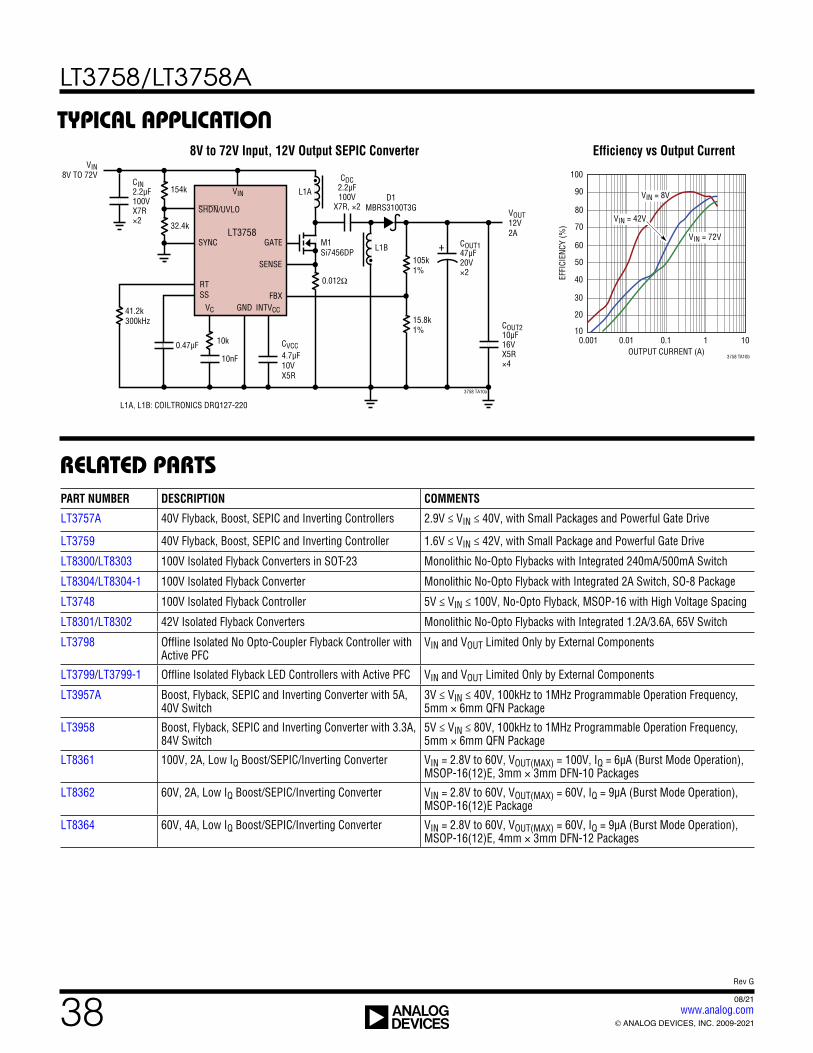
LT3758/LT3758A
38Rev G
For more information www.analog.com ANALOG DEVICES, INC. 2009-2021
08/21www.analog.com
TYPICAL APPLICATION
RELATED PARTS
8V to 72V Input, 12V Output SEPIC Converter
SENSE
LT3758
VIN
VIN8V TO 72V
CIN2.2µF100VX7R×2
CDC2.2µF100V
X7R, ×2VOUT12V2A
0.012Ω
M1Si7456DP
41.2k300kHz
GATE
FBXGND INTVCC
SHDN/UVLO
SYNC
RTSS
•
•154k
32.4k
0.47µF
10nF
10k
L1A
L1B
D1MBRS3100T3G
3758 TA10a
105k1%
15.8k1% COUT2
10µF16VX5R×4
COUT147µF20V×2
CVCC4.7µF10VX5R
L1A, L1B: COILTRONICS DRQ127-220
+
VC
Efficiency vs Output Current
VIN = 8V
OUTPUT CURRENT (A)
10
EFFI
CIEN
CY (%
)
30
20
40
50
60
70
80
90
100
3758 TA10b
0.001 0.01 0.1 1 10
VIN = 72V
VIN = 42V
PART NUMBER DESCRIPTION COMMENTS
LT3757A 40V Flyback, Boost, SEPIC and Inverting Controllers 2.9V ≤ VIN ≤ 40V, with Small Packages and Powerful Gate Drive
LT3759 40V Flyback, Boost, SEPIC and Inverting Controller 1.6V ≤ VIN ≤ 42V, with Small Package and Powerful Gate Drive
LT8300/LT8303 100V Isolated Flyback Converters in SOT-23 Monolithic No-Opto Flybacks with Integrated 240mA/500mA Switch
LT8304/LT8304-1 100V Isolated Flyback Converter Monolithic No-Opto Flyback with Integrated 2A Switch, SO-8 Package
LT3748 100V Isolated Flyback Controller 5V ≤ VIN ≤ 100V, No-Opto Flyback, MSOP-16 with High Voltage Spacing
LT8301/LT8302 42V Isolated Flyback Converters Monolithic No-Opto Flybacks with Integrated 1.2A/3.6A, 65V Switch
LT3798 Offline Isolated No Opto-Coupler Flyback Controller with Active PFC
VIN and VOUT Limited Only by External Components
LT3799/LT3799-1 Offline Isolated Flyback LED Controllers with Active PFC VIN and VOUT Limited Only by External Components
LT3957A Boost, Flyback, SEPIC and Inverting Converter with 5A, 40V Switch
3V ≤ VIN ≤ 40V, 100kHz to 1MHz Programmable Operation Frequency, 5mm × 6mm QFN Package
LT3958 Boost, Flyback, SEPIC and Inverting Converter with 3.3A, 84V Switch
5V ≤ VIN ≤ 80V, 100kHz to 1MHz Programmable Operation Frequency, 5mm × 6mm QFN Package
LT8361 100V, 2A, Low IQ Boost/SEPIC/Inverting Converter VIN = 2.8V to 60V, VOUT(MAX) = 100V, IQ = 6µA (Burst Mode Operation), MSOP-16(12)E, 3mm × 3mm DFN-10 Packages
LT8362 60V, 2A, Low IQ Boost/SEPIC/Inverting Converter VIN = 2.8V to 60V, VOUT(MAX) = 60V, IQ = 9µA (Burst Mode Operation), MSOP-16(12)E Package
LT8364 60V, 4A, Low IQ Boost/SEPIC/Inverting Converter VIN = 2.8V to 60V, VOUT(MAX) = 60V, IQ = 9µA (Burst Mode Operation), MSOP-16(12)E, 4mm × 3mm DFN-12 Packages
Related Documents