LPC29xx- Base Module

Welcome message from author
This document is posted to help you gain knowledge. Please leave a comment to let me know what you think about it! Share it to your friends and learn new things together.
Transcript

LPC29xx- Base Module

2
Agenda
Introduction
Memory support
Subsystems– PCR (Power Clock & Reset)– General (GeSS)– Networking (IVNSS)– Peripheral (PeSS)– Modulation and Sampling (MSCSS)
Power modes
DMA support
Tools
3
Introduction
ARM968E-S Overview
LPC29xx Derivatives
LPC29xx Block Diagram

4
The ARM9E Processor FamilyARM968E-S (& ARM926EJ-S)
ARMv5TE instruction set– DSP instructions
Tightly Coupled Memories– Next slide
ETM9 interface

5
Tightly coupled memory (TCM)
TCM is a low-latency memory that provides predictable performance – TCM accesses are deterministic and do not access the AHB– Cache on the other hand is not predictable
Due to its deterministic behavior, TCM can hold critical routines, such as interrupt handling routines or real-time tasks where the indeterminacy of a cache is highly undesirable
Can easily be controlled by a small footprint embedded OS– Cache requires a MUCH larger OS to manage it efficiently

6
Configuring TCM’s using Keil Tools

7
LPC29xx Family- An Introduction
Industry’s fastest running ARM968 running at 125MHz
Memory support– On-chip SRAM and Flash, EEPROM, TCM,
External Memory Interface
Key peripherals– Motor control block
• PWM, QEI, two 3.3V and one 5V ADC– 2 CAN controllers– 2 LIN controllers– USB FS OTG/Host/Device controllers
“ Industry’s Fastest ARM Flash MCU running at 125MHz ”

8
LPC29xx Derivatives

9
LPC2939Block
Diagram

10
LPC2919/01LPC2917/01
8KB ETB
QEI
I2C0/1
GP DMA
Chip Feature ID
RS485 UARTs
125MHz

11
Memory SupportSRAM
EMC
Flash
EEPROM
Booting

12
Overview
32KB or 16KB Instruction and Data TCMs
On-chip SRAM- Up to 56KB
On-chip Flash- Up to 768KB
16KB EEPROM
8KB ETB SRAM
External static memory controller

13
SRAM
56KB SRAM – 32 KB general purpose SRAM– Independent additional 16 KB
SRAM– 8KB ETB RAM
LPC2921, LPC2923, LPC2925
Memory shadowing from Flash to SRAM supported enabling faster interrupt execution from SRAM

14
External Memory Interface
8 memory banks each capable of addressing 16MB
24-bit Address and 32-bit data bus
Data bus configurable as 8-, 16- or 32-bit width
Unused data bus pins become general purpose I/O

15
Flash Memory

16
Flash Operations
Erasing: Done per sector
Burning: Programming is done per page (smallest flash write block is 16 bytes)
Protection– Sector wise write protection – JTAG interface can be disabled as well

17
Flash Features
Flash signature generation– 128-bit signature from a range of Flash memory
Flash interrupts– END_OF_BURN, END_OF_ERASE, END_OF_MISR
Index sector– JTAG access protection – Storage of customer information– Sector security
Flash endurance- 100K cycles (-25˚C to 85˚C)
Flash retention- 10 years (<100K cycles @ -40˚C to 85˚C)

18
EEPROM
256 pages= 16KB
Prerequisites for EEPROM operations– Minimum operating voltage= 1.5V– Need a 375kHz clock for erase/program
operations
EEPROM and Flash are independent modules
Page 2- 64 bytes
Page 1- 64 bytes
Page 0- 64 bytes
16KB EEPROM
Page 255- 64 bytes

19
EEPROM Operations
8-bit, 16-bit and 32-bit read operations
8-bit, 16-bit and 32-bit write operations
Erase/program page
BIST operation supported that would lead to 2 16-bit signatures
The EEPROM can be powered down

20
Memory Regions

21
Booting

22
Power, Clock & Reset Subsystem (PCRSS)
Clock Generation Unit (CGU)
Reset Generation Unit (RGU)
Power Management Unit (PMU)

23
Clock Structure: CGU0 and CGU1
CGU0 provides clocks to all the subsystems
CGU1 provides clock to the USB block and provides a clock output
Both CGUs are functionally identical

24
CGU0 Operation
CGU0
OSC1M (400 KHz osc.)
Ext Oscillator(up to 25MHz) 11 Base
Clocks

25
CGU0 Breakdown
11 Base Clocks
STAGE 1 STAGE 2 STAGE 3

26
Stage 1: PLL
PLL
2
Ext Oscillator
LP Oscillator1
To Stage 3
To Stage 3

27
LP_OSC
XTAL OSCFDIV0
FDIV6
FDIV0
FDIV6
PLL
1
3-5
2
Stage 2: Fractional Dividers

28
Stage 3: Output Registers
LP_OSC
XTAL OSC
PLL o/ps
FDIV0
FDIV6
5 ClocksStage 1
7 ClocksStage 2
OUT 0 BASE_SAFE_CLK
OUT 2 BASE_PCR_CLK
OUT 1 BASE_SYS_CLK
OUT 11 BASE_ICLK1_ CLK

29
The 11 Base ClocksBASE CLOCK DESTINATION
BASE_SAFE_CLK Watchdog timer
BASE_SYS_CLK ARM and AHB clock
BASE_PCR_CLK PCR subsystem
BASE_IVNSS_CLK Networking subsystem
BASE_MSCSS_CLK MSC subsystem
BASE_ICLK0_CLK Used by CGU1
BASE_UART_CLK Clock to UARTs
BASE_SPI_CLK Clock to SPIs
BASE_TMR_CLK Clock to Timers
BASE_ADC_CLK Clock to ADCs
BASE_ICLK1_CLK Used by CGU1
Visual Guidance on Next Slide

30
BASE_SYS_CLK
BASE_PCR_CLK
BASE_IVNSS_CLK
BASE_MSCSS_CLK
BASE_ICLK0/1_CLK
BASE_SAFE_CLKBASE_UART_CLKBASE_SPI_CLKBASE_TMR_CLK
BASE_ADC_CLK

31
CGU1
STAGE 1 STAGE 2 STAGE 3

32
RGU
LPC29xx
Watchdog
RGU
WD Reset
PCR
Cold
Warm
RGU
POR
Ext Reset
24 Individual
Resets

33
Block Resets Explained

34
RGU Summary
Activation of reset– Group reset- RGU, PCR, Cold and Warm– Provides 24 individual resets to different blocks like SPI, UART,
USB etc.
Other key functions– Monitoring – Finding the source of reset– Locking the CGU

35
PMU

36
PMU Explained
Configuration and status registers are provided for all branch clocks (except CLK_SYS_CPU, CLK_SYS & CLK_SYS_PCR)
– Individual branch clocks can be also be switched off– Individual branch clocks can be made ready for sleep mode
Using a single PD bit, all selected branch clocks can be put to sleep
Wakeup from idle mode, can be achieved with the Event router which is covered later

37
General Subsystem (GeSS)
System Control Unit (SCU)
Event Router
[Vectored Interrupt Controller]

38
SCU- Selecting Pin Function

39
Input Pads
Analog input
Digital input– With internal pull up/down– With internal pull up– With internal pull down– With bus keeper
When pull up is activated the input is NOT 5V TOLERANT

40
SCU- Memory Mapping
Shadow memory mapping registers defines which part of the memory region is present in the shadow memory area
512 MB of Shadow Memory
0x00000000
0x20000000
ARM CPU Master
DMA0 Master
DMA1 Master
Virtual Memory
USB Master

41
Event Router- What is it?
Main purpose:– Uses “events” to wake up the CGU– Uses “events” to act like an interrupt source to the VIC
Events:– External pins– Internal interrupts
Interacts with the VIC in both ways– Acts like a source of interrupt to the VIC– Or use the VIC as a source to wake up the CGU

42
Event Router
EXTINTx
CANx Rx pins
I2C Clock pins
LINx Rx pins
SPIx Rx pins
UARTx pins
USB pins
CAN interrupt
VIC IRQ
VIC FIQ

43
Vectored Interrupt Controller (VIC)

44
An Inside Look into the VIC
INT_REQUEST
register
INT_VECTOR
register
INT_PRIORITYMASK_1/0
register
INT_PENDING
register

45
Interrupt Execution (Nested & Non-Nested)
Stack workspace
INT_VECTOR reg
Execute ISR
Restore workspace
Return back to Main
INT_PRIORITY reg
Re-enable interrupts
Restore INT_PRIORITY

46
Networking Subsystem(IVNSS)
CAN
LIN
I2C

47
2 CAN Controllers- Key Features
Data rates up to 1 Mb/s, CAN 2.0B & ISO 11898 compatible
Supports Full-CAN mode and extensive message filtering
Each controller supports triple transmit buffers and double receive buffers
Error and System Diagnostics Support, Self Reception Mode & Listen Only Mode
Advanced Hardware Acceptance Filter to reduce CPU load

48
CAN Functional Description

49
Global Acceptance Filter
Uses a 2KB look-up table
The table can contain up to 1024 SFI or 512 EFI or mixture of both types
Broken up into 5 sections CAN configuration example: http://www.nxp.com/acrobat_download/applicationnotes/AN10674_1.pdf

50
LIN- An Introduction
Low cost sub network, complementing CAN and FlexRay
Single master, multiple slaves concept
Based on the UART interface
Speed up to 20Kbits/sec
Seat
Seat
Seat
SeatClimate
Brake
Brake
Brake
Brake
Lock Lock
Dashboard
Lock Lock
Lock Lock
FlexRayCANLIN

51
LIN Network
Slave Task
Master Node
Master Task
Slave Task
Slave Node
Slave Task
Slave Node

52
LIN Message Transmission
Master Task
Slave Task
Slave Task
Header Header
Response
Response

53
LIN Master Controller
4 32-bit Message buffers
Programmable sync-break from 10-16 bits
“Step-by-step example for using the LIN master”

54
2 I2C-Interfaces
400 KHz transfer rates (Fast I2C)
Easy to configure as master, slave or master/slave
Multi-master bus with arbitration control
Supports multiple address recognition and a bus monitor mode

55
Peripheral Subsystem (PeSS)
IO ports
SPIs
Timers
UARTs

56
General Purpose IO Ports
Up to 108 IO pins with programmable pull up, pull down and bus keeper
6 GPIO ports each capable of accessing up to 32 pins
The pins must be routed in the SCU

57
Timers 0/1/2/3
External Match o/p

58
Watchdog- Features
The timer registers are protected by key sequences
Two operating modes- Normal and debug
Internal chip reset when not triggered periodically- Through RGU

59
SPI 0/1/2
Master or slave operation
Supports up to four slaves in sequential multi-slave operation (next slide)
Programmable clock bit rate and pre-scaler, based on SPI source clock from the CGU
Separate transmit and receive FIFO buffers, 16-bit wide, 32 locations deep
Programmable data frame size from 4 to 16 bits
Internal loop back test mode

60
SPI Mode of Operation
Master mode– Normal transmission mode
• Software intervention needed each time a new slave needs to be addressed
– Sequential-slave mode• Will sequentially transmit data to 4
slaves as long as data is available in the FIFO
– Max. clock rate in master mode <= fclk_spi/2
Slave mode– Max. clock rate in slave mode=
fclk_spi/4

61
UART 0/1 Interfaces
Industry standard 16C550 UARTs
RS-485/9-bit mode support. Great for Multiprocessor Environment!
16 bytes FIFO message buffer for transmit and receive
Fractional divider
Standard modem interface signals included (CTS, DCD, DTS, DTR, RI, RTS)

62
MSC Subsystem(MSCSS)
PWM
ADC
QEI

63
MSCSS- The Big Picture
ADC
PWMTimers

64
PWM Blocks- Key Features
4 PWM blocks that can operate synchronously
Each PWM can produce 6 PWM outputs
Operation modes– Continuous– Burst – Trap – Run-once
Capture Functionality
Shadow register set

65
PWM Explained (1)PWM
16-bit Counter
CAPT0
CAPT1
CAPT2
CAPT3
16-bit Prescaler
6 PWM Outputs
4 PWM Capture
TRAP
SYNC_IN
Timer Carrier
TRANS_ENABLE_ IN
SYNC_OUT
TRANS_ENABLE_ OUT

66
PWM Explained (2)
67
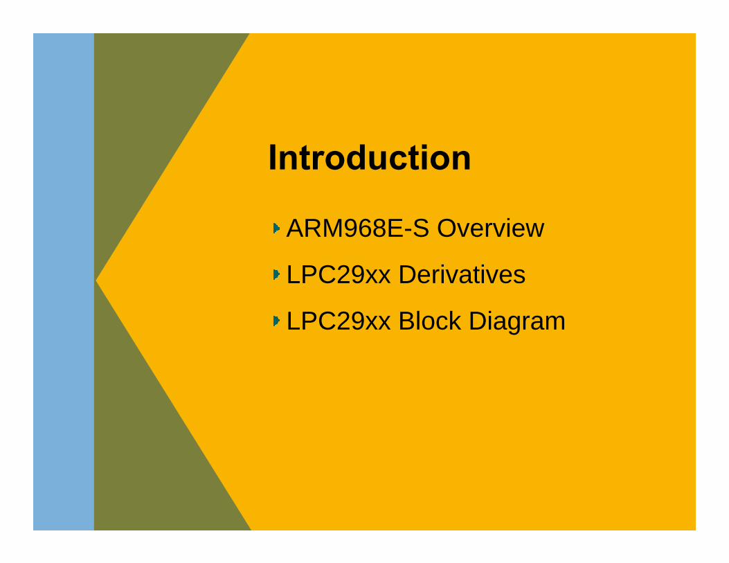
ADC- Key features
Two 10-bit ADCs, 8-channels each, with 3.3 Vmeasurement range
One 8-channel 10-bit ADC with 5.0 Vmeasurement range
Total 24 analog inputs, with conversion times as low as 2.44 μs per channel
Each channel provides a compare function to minimize interrupts

68
ADCBlock Diagram

69
ADC Start Conditions

70
MSCSS- Possible Applications
Voltage monitoring and level measurement
Synchronized PWM events
Synchronized PWM and ADC events
Dimmer application using PWMs
Sine wave generation
Comparator

71
Quadrature Encoder Interface (QEI)

72
QEI- Key Features
Tracks encoder position
Digital filter with programmable delays for encoder input signals
Programmable for 2X or 4X position counting.
Velocity capture
Index counter for revolution counting
Can combine index and position interrupts to produce an interrupt for whole and partial revolution displacement

73
Other Peripherals
GPDMA
USB FS Host/Device/OTG Controllers

74
GPDMA
Supported peripherals– SPIs– UARTs– Memory-to-memory transfers
Features:– Eight DMA channels – Internal four-word FIFO per
channel.– Supports 8, 16, and 32-bit wide
transactions– Single and burst DMA support– Scatter or gather DMA

75
USB Portfolio

76
USB Device/ Host/ OTG controllers
Device– Supports 32 physical (16 logical) endpoints– Supports Control, Bulk, Interrupt and Isochronous endpoints– Scalable realization of endpoints at run time– Supports SoftConnect and GoodLink features
Host controller– OHCI compliant– The Host Controller has four USB states visible to the SW Driver
OTG– Fully compliant with On-The-Go supplement to the USB 2.0 Specification, Revision
1.0a– Hardware support for Host Negotiation Protocol (HNP)– Includes a programmable timer required for HNP and SRP– Supports any OTG transceiver compliant with the OTG Transceiver Specification

77
Power Modes

78
Power Modes

79
Power Numbers- LPC2939

80
Tools

81
Evaluation Boards
Hitex LPC2919 Board Keil LPC2919 Board

82
Motor Control Application

83
ETM, ETB

84
Related Documents