Prelimi nary User’s Manual, V1.0, June 2007 Microcontrollers XC2000 Derivatives 16/32-Bit Single-Chip Microcontroller with 32-Bit Performance Volume 1 (of 2): System Units

Welcome message from author
This document is posted to help you gain knowledge. Please leave a comment to let me know what you think about it! Share it to your friends and learn new things together.
Transcript
Pr e
l im
i na
r y
User’s Manual , V1.0, June 2007
Microcontrol lers
XC2000 Derivat ives16/32-Bi t Single-Chip Microcontrol ler wi th 32-Bi t PerformanceVolume 1 (of 2) : System Uni ts
Edition 2007-06Published byInfineon Technologies AG81726 Munich, Germany© 2007 Infineon Technologies AGAll Rights Reserved.
Legal DisclaimerThe information given in this document shall in no event be regarded as a guarantee of conditions or characteristics. With respect to any examples or hints given herein, any typical values stated herein and/or any information regarding the application of the device, Infineon Technologies hereby disclaims any and all warranties and liabilities of any kind, including without limitation, warranties of non-infringement of intellectual property rights of any third party.
InformationFor further information on technology, delivery terms and conditions and prices, please contact the nearest Infineon Technologies Office (www.infineon.com).
WarningsDue to technical requirements, components may contain dangerous substances. For information on the types in question, please contact the nearest Infineon Technologies Office.Infineon Technologies components may be used in life-support devices or systems only with the express written approval of Infineon Technologies, if a failure of such components can reasonably be expected to cause the failure of that life-support device or system or to affect the safety or effectiveness of that device or system. Life support devices or systems are intended to be implanted in the human body or to support and/or maintain and sustain and/or protect human life. If they fail, it is reasonable to assume that the health of the user or other persons may be endangered.

Pr e
l im
i na
r y
User’s Manual , V1.0, June 2007
Microcontrol lers
XC2000 Derivat ives16/32-Bi t Single-Chip Microcontrol ler wi th 32-Bi t PerformanceVolume 1 (of 2) : System Uni ts
XC2000 DerivativesSystem Units (Vol. 1 of 2)
Preliminary
User’s Manual V1.0, 2007-06
XC2xxxRevision History: V1.0, 2007-06Previous Version(s):V0.1, 2007-03, Draft versionPage Subjects (major changes since last revision)1-2 More derivatives added to list
Description of SSC and CAN bootstrap loaders added9-1ff EBC chapter corrected
We Listen to Your CommentsAny information within this document that you feel is wrong, unclear or missing at all?Your feedback will help us to continuously improve the quality of this document.Please send your proposal (including a reference to this document) to:[email protected]
XC2000 DerivativesSystem Units (Vol. 1 of 2)
Summary Of ChaptersPreliminary
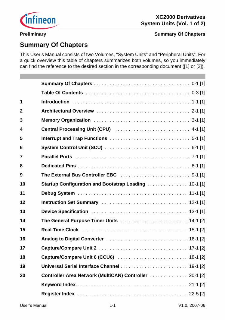
Summary Of ChaptersThis User’s Manual consists of two Volumes, “System Units” and “Peripheral Units”. For a quick overview this table of chapters summarizes both volumes, so you immediately can find the reference to the desired section in the corresponding document ([1] or [2]).
Summary Of Chapters . . . . . . . . . . . . . . . . . . . . . . . . . . . . . . . . . . . . 0-1 [1]
Table Of Contents . . . . . . . . . . . . . . . . . . . . . . . . . . . . . . . . . . . . . . . 0-3 [1]
1 Introduction . . . . . . . . . . . . . . . . . . . . . . . . . . . . . . . . . . . . . . . . . . . . 1-1 [1]
2 Architectural Overview . . . . . . . . . . . . . . . . . . . . . . . . . . . . . . . . . . . 2-1 [1]
3 Memory Organization . . . . . . . . . . . . . . . . . . . . . . . . . . . . . . . . . . . . 3-1 [1]
4 Central Processing Unit (CPU) . . . . . . . . . . . . . . . . . . . . . . . . . . . . 4-1 [1]
5 Interrupt and Trap Functions . . . . . . . . . . . . . . . . . . . . . . . . . . . . . . 5-1 [1]
6 System Control Unit (SCU) . . . . . . . . . . . . . . . . . . . . . . . . . . . . . . . . 6-1 [1]
7 Parallel Ports . . . . . . . . . . . . . . . . . . . . . . . . . . . . . . . . . . . . . . . . . . . 7-1 [1]
8 Dedicated Pins . . . . . . . . . . . . . . . . . . . . . . . . . . . . . . . . . . . . . . . . . . 8-1 [1]
9 The External Bus Controller EBC . . . . . . . . . . . . . . . . . . . . . . . . . . 9-1 [1]
10 Startup Configuration and Bootstrap Loading . . . . . . . . . . . . . . . 10-1 [1]
11 Debug System . . . . . . . . . . . . . . . . . . . . . . . . . . . . . . . . . . . . . . . . . 11-1 [1]
12 Instruction Set Summary . . . . . . . . . . . . . . . . . . . . . . . . . . . . . . . . 12-1 [1]
13 Device Specification . . . . . . . . . . . . . . . . . . . . . . . . . . . . . . . . . . . . 13-1 [1]
14 The General Purpose Timer Units . . . . . . . . . . . . . . . . . . . . . . . . . 14-1 [2]
15 Real Time Clock . . . . . . . . . . . . . . . . . . . . . . . . . . . . . . . . . . . . . . . 15-1 [2]
16 Analog to Digital Converter . . . . . . . . . . . . . . . . . . . . . . . . . . . . . . 16-1 [2]
17 Capture/Compare Unit 2 . . . . . . . . . . . . . . . . . . . . . . . . . . . . . . . . . 17-1 [2]
18 Capture/Compare Unit 6 (CCU6) . . . . . . . . . . . . . . . . . . . . . . . . . . 18-1 [2]
19 Universal Serial Interface Channel . . . . . . . . . . . . . . . . . . . . . . . . . 19-1 [2]
20 Controller Area Network (MultiCAN) Controller . . . . . . . . . . . . . . 20-1 [2]
Keyword Index . . . . . . . . . . . . . . . . . . . . . . . . . . . . . . . . . . . . . . . . . 21-1 [2]
Register Index . . . . . . . . . . . . . . . . . . . . . . . . . . . . . . . . . . . . . . . . . 22-5 [2]
User’s Manual L-1 V1.0, 2007-06
XC2000 DerivativesSystem Units (Vol. 1 of 2)
Summary Of ChaptersPreliminary
User’s Manual L-2 V1.0, 2007-06

XC2000 DerivativesSystem Units (Vol. 1 of 2)
Table Of ContentsPreliminary
Table Of ContentsThis User’s Manual consists of two Volumes, “System Units” and “Peripheral Units”. For your convenience this table of contents (and also the keyword and register index) lists both volumes, so you can immediately find the reference to the desired section in the corresponding document ([1] or [2]).
Summary Of Chapters . . . . . . . . . . . . . . . . . . . . . . . . . . . . . . . . . . . . 0-1 [1]
Table Of Contents . . . . . . . . . . . . . . . . . . . . . . . . . . . . . . . . . . . . . . . 0-3 [1]
1 Introduction . . . . . . . . . . . . . . . . . . . . . . . . . . . . . . . . . . . . . . . . . . . . 1-1 [1]1.1 Members of the 16-bit Microcontroller Family . . . . . . . . . . . . . . . . . . . 1-3 [1]1.2 Summary of Basic Features . . . . . . . . . . . . . . . . . . . . . . . . . . . . . . . . 1-5 [1]1.3 Abbreviations . . . . . . . . . . . . . . . . . . . . . . . . . . . . . . . . . . . . . . . . . . . 1-9 [1]1.4 Naming Conventions . . . . . . . . . . . . . . . . . . . . . . . . . . . . . . . . . . . . . 1-10 [1]
2 Architectural Overview . . . . . . . . . . . . . . . . . . . . . . . . . . . . . . . . . . . 2-1 [1]2.1 Basic CPU Concepts and Optimizations . . . . . . . . . . . . . . . . . . . . . . . 2-2 [1]2.1.1 High Instruction Bandwidth/Fast Execution . . . . . . . . . . . . . . . . . . . 2-4 [1]2.1.2 Powerful Execution Units . . . . . . . . . . . . . . . . . . . . . . . . . . . . . . . . . 2-5 [1]2.1.3 High Performance Branch-, Call-, and Loop-Processing . . . . . . . . . 2-6 [1]2.1.4 Consistent and Optimized Instruction Formats . . . . . . . . . . . . . . . . 2-7 [1]2.1.5 Programmable Multiple Priority Interrupt System . . . . . . . . . . . . . . 2-8 [1]2.1.6 Interfaces to System Resources . . . . . . . . . . . . . . . . . . . . . . . . . . . 2-9 [1]2.2 On-Chip System Resources . . . . . . . . . . . . . . . . . . . . . . . . . . . . . . . 2-10 [1]2.3 On-Chip Peripheral Blocks . . . . . . . . . . . . . . . . . . . . . . . . . . . . . . . . 2-15 [1]2.4 Clock Generation . . . . . . . . . . . . . . . . . . . . . . . . . . . . . . . . . . . . . . . . 2-32 [1]2.5 Power Management . . . . . . . . . . . . . . . . . . . . . . . . . . . . . . . . . . . . . . 2-33 [1]2.6 On-Chip Debug Support (OCDS) . . . . . . . . . . . . . . . . . . . . . . . . . . . 2-34 [1]
3 Memory Organization . . . . . . . . . . . . . . . . . . . . . . . . . . . . . . . . . . . . 3-1 [1]3.1 Address Mapping . . . . . . . . . . . . . . . . . . . . . . . . . . . . . . . . . . . . . . . . . 3-3 [1]3.2 Special Function Register Areas . . . . . . . . . . . . . . . . . . . . . . . . . . . . . 3-4 [1]3.3 Data Memory Areas . . . . . . . . . . . . . . . . . . . . . . . . . . . . . . . . . . . . . . . 3-9 [1]3.4 Program Memory Areas . . . . . . . . . . . . . . . . . . . . . . . . . . . . . . . . . . . 3-11 [1]3.4.1 Program/Data SRAM (PSRAM) . . . . . . . . . . . . . . . . . . . . . . . . . . . 3-12 [1]3.4.2 Non-Volatile Program Memory (Flash) . . . . . . . . . . . . . . . . . . . . . 3-13 [1]3.5 System Stack . . . . . . . . . . . . . . . . . . . . . . . . . . . . . . . . . . . . . . . . . . . 3-14 [1]3.6 IO Areas . . . . . . . . . . . . . . . . . . . . . . . . . . . . . . . . . . . . . . . . . . . . . . . 3-15 [1]3.7 External Memory Space . . . . . . . . . . . . . . . . . . . . . . . . . . . . . . . . . . 3-16 [1]3.8 Crossing Memory Boundaries . . . . . . . . . . . . . . . . . . . . . . . . . . . . . . 3-17 [1]3.9 Embedded Flash Memory . . . . . . . . . . . . . . . . . . . . . . . . . . . . . . . . . 3-18 [1]3.9.1 Definitions . . . . . . . . . . . . . . . . . . . . . . . . . . . . . . . . . . . . . . . . . . . 3-18 [1]
User’s Manual L-3 V1.0, 2007-06
XC2000 DerivativesSystem Units (Vol. 1 of 2)
Table Of ContentsPreliminary
3.9.2 Operating Modes . . . . . . . . . . . . . . . . . . . . . . . . . . . . . . . . . . . . . . 3-20 [1]3.9.3 Operations . . . . . . . . . . . . . . . . . . . . . . . . . . . . . . . . . . . . . . . . . . . 3-22 [1]3.9.4 Details of Command Sequences . . . . . . . . . . . . . . . . . . . . . . . . . . 3-25 [1]3.9.5 Data Integrity . . . . . . . . . . . . . . . . . . . . . . . . . . . . . . . . . . . . . . . . . 3-35 [1]3.9.6 Protection Handling Details . . . . . . . . . . . . . . . . . . . . . . . . . . . . . . 3-38 [1]3.9.7 Protection Handling Examples . . . . . . . . . . . . . . . . . . . . . . . . . . . . 3-45 [1]3.9.8 EEPROM Emulation . . . . . . . . . . . . . . . . . . . . . . . . . . . . . . . . . . . 3-47 [1]3.9.9 Interrupt Generation . . . . . . . . . . . . . . . . . . . . . . . . . . . . . . . . . . . . 3-49 [1]3.10 On-Chip Program Memory Control . . . . . . . . . . . . . . . . . . . . . . . . . . 3-50 [1]3.10.1 Overview . . . . . . . . . . . . . . . . . . . . . . . . . . . . . . . . . . . . . . . . . . . . 3-50 [1]3.10.2 Register Interface . . . . . . . . . . . . . . . . . . . . . . . . . . . . . . . . . . . . . 3-52 [1]3.10.3 Startup, Shutdown . . . . . . . . . . . . . . . . . . . . . . . . . . . . . . . . . . . . . 3-67 [1]3.10.4 Error Reporting Summary . . . . . . . . . . . . . . . . . . . . . . . . . . . . . . . 3-69 [1]3.11 Data Retention Memories . . . . . . . . . . . . . . . . . . . . . . . . . . . . . . . . . 3-70 [1]3.11.1 Stand-By RAM Accesses . . . . . . . . . . . . . . . . . . . . . . . . . . . . . . . . 3-71 [1]3.11.2 Stand-By RAM Registers . . . . . . . . . . . . . . . . . . . . . . . . . . . . . . . . 3-72 [1]3.11.3 Marker Memory (MKMEM) . . . . . . . . . . . . . . . . . . . . . . . . . . . . . . 3-76 [1]3.12 Memory Parity Error Handling . . . . . . . . . . . . . . . . . . . . . . . . . . . . . . 3-77 [1]3.12.1 Parity Control Registers . . . . . . . . . . . . . . . . . . . . . . . . . . . . . . . . . 3-78 [1]
4 Central Processing Unit (CPU) . . . . . . . . . . . . . . . . . . . . . . . . . . . . 4-1 [1]4.1 Components of the CPU . . . . . . . . . . . . . . . . . . . . . . . . . . . . . . . . . . . 4-4 [1]4.2 Instruction Fetch and Program Flow Control . . . . . . . . . . . . . . . . . . . . 4-5 [1]4.2.1 Branch Detection and Branch Prediction Rules . . . . . . . . . . . . . . . . 4-7 [1]4.2.2 Correctly Predicted Instruction Flow . . . . . . . . . . . . . . . . . . . . . . . . 4-7 [1]4.2.3 Incorrectly Predicted Instruction Flow . . . . . . . . . . . . . . . . . . . . . . . 4-9 [1]4.3 Instruction Processing Pipeline . . . . . . . . . . . . . . . . . . . . . . . . . . . . . 4-11 [1]4.3.1 Pipeline Conflicts Using General Purpose Registers . . . . . . . . . . . 4-13 [1]4.3.2 Pipeline Conflicts Using Indirect Addressing Modes . . . . . . . . . . . 4-15 [1]4.3.3 Pipeline Conflicts Due to Memory Bandwidth . . . . . . . . . . . . . . . . 4-17 [1]4.3.4 Pipeline Conflicts Caused by CPU-SFR Updates . . . . . . . . . . . . . 4-20 [1]4.4 CPU Configuration Registers . . . . . . . . . . . . . . . . . . . . . . . . . . . . . . 4-26 [1]4.5 Use of General Purpose Registers . . . . . . . . . . . . . . . . . . . . . . . . . . 4-29 [1]4.5.1 GPR Addressing Modes . . . . . . . . . . . . . . . . . . . . . . . . . . . . . . . . 4-31 [1]4.5.2 Context Switching . . . . . . . . . . . . . . . . . . . . . . . . . . . . . . . . . . . . . 4-33 [1]4.6 Code Addressing . . . . . . . . . . . . . . . . . . . . . . . . . . . . . . . . . . . . . . . . 4-37 [1]4.7 Data Addressing . . . . . . . . . . . . . . . . . . . . . . . . . . . . . . . . . . . . . . . . 4-39 [1]4.7.1 Short Addressing Modes . . . . . . . . . . . . . . . . . . . . . . . . . . . . . . . . 4-39 [1]4.7.2 Long Addressing Modes . . . . . . . . . . . . . . . . . . . . . . . . . . . . . . . . 4-41 [1]4.7.3 Indirect Addressing Modes . . . . . . . . . . . . . . . . . . . . . . . . . . . . . . 4-44 [1]4.7.4 DSP Addressing Modes . . . . . . . . . . . . . . . . . . . . . . . . . . . . . . . . . 4-46 [1]4.7.5 The System Stack . . . . . . . . . . . . . . . . . . . . . . . . . . . . . . . . . . . . . 4-52 [1]4.8 Standard Data Processing . . . . . . . . . . . . . . . . . . . . . . . . . . . . . . . . . 4-56 [1]
User’s Manual L-4 V1.0, 2007-06
XC2000 DerivativesSystem Units (Vol. 1 of 2)
Table Of ContentsPreliminary
4.8.1 16-bit Adder/Subtracter, Barrel Shifter, and 16-bit Logic Unit . . . . 4-60 [1]4.8.2 Bit Manipulation Unit . . . . . . . . . . . . . . . . . . . . . . . . . . . . . . . . . . . 4-60 [1]4.8.3 Multiply and Divide Unit . . . . . . . . . . . . . . . . . . . . . . . . . . . . . . . . 4-62 [1]4.9 DSP Data Processing (MAC Unit) . . . . . . . . . . . . . . . . . . . . . . . . . . . 4-64 [1]4.9.1 MAC Unit Control . . . . . . . . . . . . . . . . . . . . . . . . . . . . . . . . . . . . . . 4-65 [1]4.9.2 Representation of Numbers and Rounding . . . . . . . . . . . . . . . . . . 4-65 [1]4.9.3 The 16-bit by 16-bit Signed/Unsigned Multiplier and Scaler . . . . . 4-66 [1]4.9.4 Concatenation Unit . . . . . . . . . . . . . . . . . . . . . . . . . . . . . . . . . . . . 4-66 [1]4.9.5 One-bit Scaler . . . . . . . . . . . . . . . . . . . . . . . . . . . . . . . . . . . . . . . . 4-66 [1]4.9.6 The 40-bit Adder/Subtracter . . . . . . . . . . . . . . . . . . . . . . . . . . . . . 4-66 [1]4.9.7 The Data Limiter . . . . . . . . . . . . . . . . . . . . . . . . . . . . . . . . . . . . . . 4-67 [1]4.9.8 The Accumulator Shifter . . . . . . . . . . . . . . . . . . . . . . . . . . . . . . . . 4-67 [1]4.9.9 The 40-bit Signed Accumulator Register . . . . . . . . . . . . . . . . . . . . 4-68 [1]4.9.10 The MAC Unit Status Word MSW . . . . . . . . . . . . . . . . . . . . . . . . . 4-70 [1]4.9.11 The Repeat Counter MRW . . . . . . . . . . . . . . . . . . . . . . . . . . . . . . 4-72 [1]4.10 Constant Registers . . . . . . . . . . . . . . . . . . . . . . . . . . . . . . . . . . . . . . 4-74 [1]
5 Interrupt and Trap Functions . . . . . . . . . . . . . . . . . . . . . . . . . . . . . . 5-1 [1]5.1 Interrupt System Structure . . . . . . . . . . . . . . . . . . . . . . . . . . . . . . . . . . 5-2 [1]5.2 Interrupt Arbitration and Control . . . . . . . . . . . . . . . . . . . . . . . . . . . . . 5-4 [1]5.3 Interrupt Vector Table . . . . . . . . . . . . . . . . . . . . . . . . . . . . . . . . . . . . 5-10 [1]5.4 Operation of the Peripheral Event Controller Channels . . . . . . . . . . 5-19 [1]5.4.1 The PECC Registers . . . . . . . . . . . . . . . . . . . . . . . . . . . . . . . . . . . 5-19 [1]5.4.2 The PEC Source and Destination Pointers . . . . . . . . . . . . . . . . . . 5-23 [1]5.4.3 PEC Transfer Control . . . . . . . . . . . . . . . . . . . . . . . . . . . . . . . . . . 5-25 [1]5.4.4 Channel Link Mode for Data Chaining . . . . . . . . . . . . . . . . . . . . . . 5-27 [1]5.4.5 PEC Interrupt Control . . . . . . . . . . . . . . . . . . . . . . . . . . . . . . . . . . 5-28 [1]5.5 Prioritization of Interrupt and PEC Service Requests . . . . . . . . . . . . 5-30 [1]5.6 Context Switching and Saving Status . . . . . . . . . . . . . . . . . . . . . . . . 5-32 [1]5.7 Interrupt Node Sharing . . . . . . . . . . . . . . . . . . . . . . . . . . . . . . . . . . . 5-35 [1]5.8 External Interrupts . . . . . . . . . . . . . . . . . . . . . . . . . . . . . . . . . . . . . . 5-36 [1]5.9 OCDS Requests . . . . . . . . . . . . . . . . . . . . . . . . . . . . . . . . . . . . . . . . 5-38 [1]5.10 Service Request Latency . . . . . . . . . . . . . . . . . . . . . . . . . . . . . . . . . 5-39 [1]5.11 Trap Functions . . . . . . . . . . . . . . . . . . . . . . . . . . . . . . . . . . . . . . . . . 5-41 [1]
6 System Control Unit (SCU) . . . . . . . . . . . . . . . . . . . . . . . . . . . . . . . . 6-1 [1]6.1 Clock Generation Unit . . . . . . . . . . . . . . . . . . . . . . . . . . . . . . . . . . . . . 6-2 [1]6.1.1 Wake-Up Clock Circuit (OSC_WU) . . . . . . . . . . . . . . . . . . . . . . . . . 6-3 [1]6.1.2 High Precision Oscillator Circuit (OSC_HP) . . . . . . . . . . . . . . . . . . 6-3 [1]6.1.3 Phase-Locked Loop (PLL) Module . . . . . . . . . . . . . . . . . . . . . . . . . 6-5 [1]6.1.4 Clock Control Unit . . . . . . . . . . . . . . . . . . . . . . . . . . . . . . . . . . . . . 6-13 [1]6.1.5 External Clock Output . . . . . . . . . . . . . . . . . . . . . . . . . . . . . . . . . . 6-15 [1]6.1.6 CGU Registers . . . . . . . . . . . . . . . . . . . . . . . . . . . . . . . . . . . . . . . . 6-18 [1]6.2 Reset Operation . . . . . . . . . . . . . . . . . . . . . . . . . . . . . . . . . . . . . . . . . 6-33 [1]
User’s Manual L-5 V1.0, 2007-06
XC2000 DerivativesSystem Units (Vol. 1 of 2)
Table Of ContentsPreliminary
6.2.1 Reset Architecture . . . . . . . . . . . . . . . . . . . . . . . . . . . . . . . . . . . . . 6-33 [1]6.2.2 General Reset Operation . . . . . . . . . . . . . . . . . . . . . . . . . . . . . . . . 6-33 [1]6.2.3 Coupling of Reset Types . . . . . . . . . . . . . . . . . . . . . . . . . . . . . . . . 6-35 [1]6.2.4 Debug Reset Assertion . . . . . . . . . . . . . . . . . . . . . . . . . . . . . . . . . 6-36 [1]6.2.5 Example1: . . . . . . . . . . . . . . . . . . . . . . . . . . . . . . . . . . . . . . . . . . . 6-36 [1]6.2.6 Example2: . . . . . . . . . . . . . . . . . . . . . . . . . . . . . . . . . . . . . . . . . . . 6-36 [1]6.2.7 Example3: . . . . . . . . . . . . . . . . . . . . . . . . . . . . . . . . . . . . . . . . . . . 6-36 [1]6.2.8 Reset Request Trigger Sources . . . . . . . . . . . . . . . . . . . . . . . . . . 6-36 [1]6.2.9 Module Reset Behavior . . . . . . . . . . . . . . . . . . . . . . . . . . . . . . . . . 6-40 [1]6.2.10 Reset Controller Registers . . . . . . . . . . . . . . . . . . . . . . . . . . . . . . . 6-41 [1]6.3 External Service Request (ESR) Pins . . . . . . . . . . . . . . . . . . . . . . . . 6-52 [1]6.3.1 General Operation . . . . . . . . . . . . . . . . . . . . . . . . . . . . . . . . . . . . . 6-52 [1]6.3.2 ESR Control Registers . . . . . . . . . . . . . . . . . . . . . . . . . . . . . . . . . . 6-58 [1]6.3.3 ESR Data Register . . . . . . . . . . . . . . . . . . . . . . . . . . . . . . . . . . . . 6-63 [1]6.4 External Request Unit (ERU) . . . . . . . . . . . . . . . . . . . . . . . . . . . . . . . 6-64 [1]6.4.1 Introduction . . . . . . . . . . . . . . . . . . . . . . . . . . . . . . . . . . . . . . . . . . 6-64 [1]6.4.2 ERU Pin Connections . . . . . . . . . . . . . . . . . . . . . . . . . . . . . . . . . . 6-66 [1]6.4.3 External Request Select Unit (ERSx; x = 0..3) . . . . . . . . . . . . . . . 6-72 [1]6.4.4 Event Trigger Logic (ETLx; x = 0..3) . . . . . . . . . . . . . . . . . . . . . . . 6-74 [1]6.4.5 Connecting Matrix . . . . . . . . . . . . . . . . . . . . . . . . . . . . . . . . . . . . . 6-76 [1]6.4.6 Output Gating Unit (OGUy; y = 0..3) . . . . . . . . . . . . . . . . . . . . . . . 6-77 [1]6.4.7 ERU Output Connections . . . . . . . . . . . . . . . . . . . . . . . . . . . . . . . 6-81 [1]6.4.8 ERU Registers . . . . . . . . . . . . . . . . . . . . . . . . . . . . . . . . . . . . . . . . 6-83 [1]6.5 Power Supply and Control . . . . . . . . . . . . . . . . . . . . . . . . . . . . . . . . . 6-90 [1]6.5.1 Supply Watchdog (SWD) . . . . . . . . . . . . . . . . . . . . . . . . . . . . . . . . 6-91 [1]6.5.2 Monitoring the Voltage Level of a Core Domain . . . . . . . . . . . . . . 6-97 [1]6.5.3 Controlling the Voltage Level of a Core Domain . . . . . . . . . . . . . 6-115 [1]6.5.4 Handling the Power System . . . . . . . . . . . . . . . . . . . . . . . . . . . . 6-126 [1]6.5.5 Power State Controller (PSC) . . . . . . . . . . . . . . . . . . . . . . . . . . . 6-128 [1]6.5.6 Operating a Power Transfer . . . . . . . . . . . . . . . . . . . . . . . . . . . . 6-130 [1]6.5.7 Power Control Registers . . . . . . . . . . . . . . . . . . . . . . . . . . . . . . . 6-134 [1]6.6 Global State Controller (GSC) . . . . . . . . . . . . . . . . . . . . . . . . . . . . . 6-156 [1]6.6.1 GSC Control Flow . . . . . . . . . . . . . . . . . . . . . . . . . . . . . . . . . . . . 6-156 [1]6.6.2 GSC Registers . . . . . . . . . . . . . . . . . . . . . . . . . . . . . . . . . . . . . . . 6-160 [1]6.7 Temperature Compensation Unit . . . . . . . . . . . . . . . . . . . . . . . . . . 6-165 [1]6.7.1 Temperature Compensation Registers . . . . . . . . . . . . . . . . . . . . 6-166 [1]6.8 Watchdog Timer . . . . . . . . . . . . . . . . . . . . . . . . . . . . . . . . . . . . . . . 6-168 [1]6.8.1 Introduction . . . . . . . . . . . . . . . . . . . . . . . . . . . . . . . . . . . . . . . . . 6-168 [1]6.8.2 Overview . . . . . . . . . . . . . . . . . . . . . . . . . . . . . . . . . . . . . . . . . . . 6-168 [1]6.8.3 Functional Description . . . . . . . . . . . . . . . . . . . . . . . . . . . . . . . . . 6-169 [1]6.8.4 WDT Kernel Registers . . . . . . . . . . . . . . . . . . . . . . . . . . . . . . . . . 6-173 [1]6.9 Wake-up Timer (WUT) . . . . . . . . . . . . . . . . . . . . . . . . . . . . . . . . . . . 6-176 [1]6.9.1 Wake-Up Timer Operation . . . . . . . . . . . . . . . . . . . . . . . . . . . . . . 6-177 [1]
User’s Manual L-6 V1.0, 2007-06
XC2000 DerivativesSystem Units (Vol. 1 of 2)
Table Of ContentsPreliminary
6.9.2 WUT Registers . . . . . . . . . . . . . . . . . . . . . . . . . . . . . . . . . . . . . . 6-178 [1]6.10 Register Control . . . . . . . . . . . . . . . . . . . . . . . . . . . . . . . . . . . . . . . . 6-181 [1]6.10.1 Register Access Control . . . . . . . . . . . . . . . . . . . . . . . . . . . . . . . 6-181 [1]6.10.2 Register Protection Registers . . . . . . . . . . . . . . . . . . . . . . . . . . . 6-183 [1]6.10.3 Miscellaneous System Control Registers . . . . . . . . . . . . . . . . . . 6-185 [1]6.11 SCU Interrupt and Trap Handling . . . . . . . . . . . . . . . . . . . . . . . . . . 6-186 [1]6.11.1 SCU Interrupt Handling . . . . . . . . . . . . . . . . . . . . . . . . . . . . . . . . 6-187 [1]6.11.2 SCU Interrupt Control Registers . . . . . . . . . . . . . . . . . . . . . . . . . 6-189 [1]6.11.3 SCU Trap Generation . . . . . . . . . . . . . . . . . . . . . . . . . . . . . . . . . 6-200 [1]6.11.4 SCU Trap Control Registers . . . . . . . . . . . . . . . . . . . . . . . . . . . . 6-202 [1]6.11.5 DPM_M Interrupt and Trap Support . . . . . . . . . . . . . . . . . . . . . . 6-210 [1]6.11.6 DPM_M Interrupt and Trap Registers . . . . . . . . . . . . . . . . . . . . . 6-211 [1]6.11.7 Alternate Interrupt Assignment Register . . . . . . . . . . . . . . . . . . . 6-216 [1]6.12 Identification Block . . . . . . . . . . . . . . . . . . . . . . . . . . . . . . . . . . . . . . 6-218 [1]6.13 SCU Register Addresses . . . . . . . . . . . . . . . . . . . . . . . . . . . . . . . . . 6-220 [1]
7 Parallel Ports . . . . . . . . . . . . . . . . . . . . . . . . . . . . . . . . . . . . . . . . . . . 7-1 [1]7.1 General Description . . . . . . . . . . . . . . . . . . . . . . . . . . . . . . . . . . . . . . . 7-2 [1]7.1.1 Basic Port Operation . . . . . . . . . . . . . . . . . . . . . . . . . . . . . . . . . . . . 7-2 [1]7.1.2 Input Stage Control . . . . . . . . . . . . . . . . . . . . . . . . . . . . . . . . . . . . . 7-5 [1]7.1.3 Output Driver Control . . . . . . . . . . . . . . . . . . . . . . . . . . . . . . . . . . . . 7-5 [1]7.2 Pin Description . . . . . . . . . . . . . . . . . . . . . . . . . . . . . . . . . . . . . . . . . . . 7-6 [1]7.2.1 Description Scheme for the Port IO Functions . . . . . . . . . . . . . . . . 7-6 [1]7.3 Port Description . . . . . . . . . . . . . . . . . . . . . . . . . . . . . . . . . . . . . . . . . . 7-7 [1]7.3.1 Port Register Description . . . . . . . . . . . . . . . . . . . . . . . . . . . . . . . . . 7-7 [1]7.3.2 Port 0 . . . . . . . . . . . . . . . . . . . . . . . . . . . . . . . . . . . . . . . . . . . . . . . 7-18 [1]7.3.3 Port 1 . . . . . . . . . . . . . . . . . . . . . . . . . . . . . . . . . . . . . . . . . . . . . . . 7-22 [1]7.3.4 Port 2 . . . . . . . . . . . . . . . . . . . . . . . . . . . . . . . . . . . . . . . . . . . . . . . 7-26 [1]7.3.5 Port 3 . . . . . . . . . . . . . . . . . . . . . . . . . . . . . . . . . . . . . . . . . . . . . . . 7-33 [1]7.3.6 Port 4 . . . . . . . . . . . . . . . . . . . . . . . . . . . . . . . . . . . . . . . . . . . . . . . 7-37 [1]7.3.7 Port 5 . . . . . . . . . . . . . . . . . . . . . . . . . . . . . . . . . . . . . . . . . . . . . . . 7-41 [1]7.3.8 Port 6 . . . . . . . . . . . . . . . . . . . . . . . . . . . . . . . . . . . . . . . . . . . . . . . 7-43 [1]7.3.9 Port 7 . . . . . . . . . . . . . . . . . . . . . . . . . . . . . . . . . . . . . . . . . . . . . . . 7-46 [1]7.3.10 Port 8 . . . . . . . . . . . . . . . . . . . . . . . . . . . . . . . . . . . . . . . . . . . . . . . 7-49 [1]7.3.11 Port 9 . . . . . . . . . . . . . . . . . . . . . . . . . . . . . . . . . . . . . . . . . . . . . . . 7-52 [1]7.3.12 Port 10 . . . . . . . . . . . . . . . . . . . . . . . . . . . . . . . . . . . . . . . . . . . . . . 7-55 [1]7.3.13 Port 11 . . . . . . . . . . . . . . . . . . . . . . . . . . . . . . . . . . . . . . . . . . . . . . 7-62 [1]7.3.14 Port 15 . . . . . . . . . . . . . . . . . . . . . . . . . . . . . . . . . . . . . . . . . . . . . . 7-65 [1]
8 Dedicated Pins . . . . . . . . . . . . . . . . . . . . . . . . . . . . . . . . . . . . . . . . . . 8-1 [1]
9 The External Bus Controller EBC . . . . . . . . . . . . . . . . . . . . . . . . . . 9-1 [1]9.1 External Bus Signals . . . . . . . . . . . . . . . . . . . . . . . . . . . . . . . . . . . . . . 9-3 [1]9.2 Timing Principles . . . . . . . . . . . . . . . . . . . . . . . . . . . . . . . . . . . . . . . . . 9-4 [1]
User’s Manual L-7 V1.0, 2007-06

XC2000 DerivativesSystem Units (Vol. 1 of 2)
Table Of ContentsPreliminary
9.2.1 Basic Bus Cycle Protocols . . . . . . . . . . . . . . . . . . . . . . . . . . . . . . . . 9-4 [1]9.2.2 Bus Cycle Phases . . . . . . . . . . . . . . . . . . . . . . . . . . . . . . . . . . . . . . 9-7 [1]9.2.3 Bus Cycle Examples: Fastest Access Cycles . . . . . . . . . . . . . . . . . 9-9 [1]9.3 Functional Description . . . . . . . . . . . . . . . . . . . . . . . . . . . . . . . . . . . . 9-11 [1]9.3.1 Configuration Register Overview . . . . . . . . . . . . . . . . . . . . . . . . . . 9-11 [1]9.3.2 The EBC Mode Register 0 . . . . . . . . . . . . . . . . . . . . . . . . . . . . . . . 9-13 [1]9.3.3 The EBC Mode Register 1 . . . . . . . . . . . . . . . . . . . . . . . . . . . . . . . 9-15 [1]9.3.4 The Timing Configuration Registers TCONCSx . . . . . . . . . . . . . . 9-16 [1]9.3.5 The Function Configuration Registers FCONCSx . . . . . . . . . . . . . 9-19 [1]9.3.6 The Address Window Selection Registers ADDRSELx . . . . . . . . . 9-22 [1]9.3.7 Ready Controlled Bus Cycles . . . . . . . . . . . . . . . . . . . . . . . . . . . . 9-25 [1]9.3.8 Access Control to LXBus Modules . . . . . . . . . . . . . . . . . . . . . . . . 9-27 [1]9.3.9 External Bus Arbitration . . . . . . . . . . . . . . . . . . . . . . . . . . . . . . . . . 9-28 [1]9.3.10 Shutdown Control . . . . . . . . . . . . . . . . . . . . . . . . . . . . . . . . . . . . . 9-32 [1]9.4 LXBus Access Control and Signal Generation . . . . . . . . . . . . . . . . . 9-33 [1]9.5 EBC Register Table . . . . . . . . . . . . . . . . . . . . . . . . . . . . . . . . . . . . . . 9-33 [1]
10 Startup Configuration and Bootstrap Loading . . . . . . . . . . . . . . . 10-1 [1]10.1 Start-Up Mode Selection . . . . . . . . . . . . . . . . . . . . . . . . . . . . . . . . . . 10-1 [1]10.2 Internal Start . . . . . . . . . . . . . . . . . . . . . . . . . . . . . . . . . . . . . . . . . . . 10-2 [1]10.3 External Start . . . . . . . . . . . . . . . . . . . . . . . . . . . . . . . . . . . . . . . . . . . 10-2 [1]10.4 Bootstrap Loading . . . . . . . . . . . . . . . . . . . . . . . . . . . . . . . . . . . . . . . 10-4 [1]10.4.1 General Functionality . . . . . . . . . . . . . . . . . . . . . . . . . . . . . . . . . . . 10-4 [1]10.4.2 Standard UART Bootstrap Loader . . . . . . . . . . . . . . . . . . . . . . . . . 10-6 [1]10.4.3 Synchronous Serial Channel Bootstrap Loader . . . . . . . . . . . . . . 10-11 [1]10.4.4 CAN Bootstrap Loader . . . . . . . . . . . . . . . . . . . . . . . . . . . . . . . . . 10-14 [1]10.4.5 Summary of Bootstrap Loader Modes . . . . . . . . . . . . . . . . . . . . . 10-17 [1]
11 Debug System . . . . . . . . . . . . . . . . . . . . . . . . . . . . . . . . . . . . . . . . . 11-1 [1]11.1 Debug Interface . . . . . . . . . . . . . . . . . . . . . . . . . . . . . . . . . . . . . . . . . 11-2 [1]11.1.1 Routing of Debug Signals . . . . . . . . . . . . . . . . . . . . . . . . . . . . . . . 11-3 [1]11.2 OCDS Module . . . . . . . . . . . . . . . . . . . . . . . . . . . . . . . . . . . . . . . . . . 11-5 [1]11.2.1 Debug Events . . . . . . . . . . . . . . . . . . . . . . . . . . . . . . . . . . . . . . . . 11-7 [1]11.2.2 Debug Actions . . . . . . . . . . . . . . . . . . . . . . . . . . . . . . . . . . . . . . . . 11-8 [1]11.3 Cerberus . . . . . . . . . . . . . . . . . . . . . . . . . . . . . . . . . . . . . . . . . . . . . . 11-9 [1]11.3.1 Functional Overview . . . . . . . . . . . . . . . . . . . . . . . . . . . . . . . . . . . 11-9 [1]
12 Instruction Set Summary . . . . . . . . . . . . . . . . . . . . . . . . . . . . . . . . 12-1 [1]
13 Device Specification . . . . . . . . . . . . . . . . . . . . . . . . . . . . . . . . . . . . 13-1 [1]
14 The General Purpose Timer Units . . . . . . . . . . . . . . . . . . . . . . . . . 14-1 [2]14.1 Timer Block GPT1 . . . . . . . . . . . . . . . . . . . . . . . . . . . . . . . . . . . . . . 14-2 [2]14.1.1 GPT1 Core Timer T3 Control . . . . . . . . . . . . . . . . . . . . . . . . . . . . 14-4 [2]14.1.2 GPT1 Core Timer T3 Operating Modes . . . . . . . . . . . . . . . . . . . . . 14-8 [2]
User’s Manual L-8 V1.0, 2007-06
XC2000 DerivativesSystem Units (Vol. 1 of 2)
Table Of ContentsPreliminary
14.1.3 GPT1 Auxiliary Timers T2/T4 Control . . . . . . . . . . . . . . . . . . . . . 14-15 [2]14.1.4 GPT1 Auxiliary Timers T2/T4 Operating Modes . . . . . . . . . . . . . 14-18 [2]14.1.5 GPT1 Clock Signal Control . . . . . . . . . . . . . . . . . . . . . . . . . . . . . 14-27 [2]14.1.6 GPT1 Timer Registers . . . . . . . . . . . . . . . . . . . . . . . . . . . . . . . . . 14-30 [2]14.1.7 Interrupt Control for GPT1 Timers . . . . . . . . . . . . . . . . . . . . . . . . 14-31 [2]14.2 Timer Block GPT2 . . . . . . . . . . . . . . . . . . . . . . . . . . . . . . . . . . . . . 14-32 [2]14.2.1 GPT2 Core Timer T6 Control . . . . . . . . . . . . . . . . . . . . . . . . . . . 14-34 [2]14.2.2 GPT2 Core Timer T6 Operating Modes . . . . . . . . . . . . . . . . . . . . 14-38 [2]14.2.3 GPT2 Auxiliary Timer T5 Control . . . . . . . . . . . . . . . . . . . . . . . . 14-41 [2]14.2.4 GPT2 Auxiliary Timer T5 Operating Modes . . . . . . . . . . . . . . . . . 14-44 [2]14.2.5 GPT2 Register CAPREL Operating Modes . . . . . . . . . . . . . . . . . 14-48 [2]14.2.6 GPT2 Clock Signal Control . . . . . . . . . . . . . . . . . . . . . . . . . . . . . 14-53 [2]14.2.7 GPT2 Timer Registers . . . . . . . . . . . . . . . . . . . . . . . . . . . . . . . . . 14-56 [2]14.2.8 Interrupt Control for GPT2 Timers and CAPREL . . . . . . . . . . . . . 14-57 [2]14.2.9 KSCCFG Register . . . . . . . . . . . . . . . . . . . . . . . . . . . . . . . . . . . . 14-58 [2]14.3 Interfaces of the GPT Module . . . . . . . . . . . . . . . . . . . . . . . . . . . . . 14-60 [2]
15 Real Time Clock . . . . . . . . . . . . . . . . . . . . . . . . . . . . . . . . . . . . . . . 15-1 [2]15.1 Defining the RTC Time Base . . . . . . . . . . . . . . . . . . . . . . . . . . . . . . . 15-2 [2]15.2 RTC Run Control . . . . . . . . . . . . . . . . . . . . . . . . . . . . . . . . . . . . . . . . 15-5 [2]15.3 RTC Operating Modes . . . . . . . . . . . . . . . . . . . . . . . . . . . . . . . . . . . . 15-7 [2]15.4 48-bit Timer Operation . . . . . . . . . . . . . . . . . . . . . . . . . . . . . . . . . . . 15-11 [2]15.5 System Clock Operation . . . . . . . . . . . . . . . . . . . . . . . . . . . . . . . . . 15-11 [2]15.6 Cyclic Interrupt Generation . . . . . . . . . . . . . . . . . . . . . . . . . . . . . . . 15-12 [2]15.7 RTC Interrupt Generation . . . . . . . . . . . . . . . . . . . . . . . . . . . . . . . . 15-13 [2]15.8 KSCCFG Register . . . . . . . . . . . . . . . . . . . . . . . . . . . . . . . . . . . . . . 15-15 [2]
16 Analog to Digital Converter . . . . . . . . . . . . . . . . . . . . . . . . . . . . . . 16-1 [2]16.1 Introduction . . . . . . . . . . . . . . . . . . . . . . . . . . . . . . . . . . . . . . . . . . . . 16-1 [2]16.1.1 ADC Block Diagram . . . . . . . . . . . . . . . . . . . . . . . . . . . . . . . . . . . . 16-2 [2]16.1.2 Feature Set . . . . . . . . . . . . . . . . . . . . . . . . . . . . . . . . . . . . . . . . . . 16-3 [2]16.1.3 Abbreviations . . . . . . . . . . . . . . . . . . . . . . . . . . . . . . . . . . . . . . . . . 16-4 [2]16.1.4 ADC Kernel Overview . . . . . . . . . . . . . . . . . . . . . . . . . . . . . . . . . . 16-5 [2]16.1.5 Conversion Request Unit . . . . . . . . . . . . . . . . . . . . . . . . . . . . . . . . 16-7 [2]16.1.6 Conversion Result Unit . . . . . . . . . . . . . . . . . . . . . . . . . . . . . . . . . 16-9 [2]16.1.7 Interrupt Structure . . . . . . . . . . . . . . . . . . . . . . . . . . . . . . . . . . . . 16-10 [2]16.1.8 Electrical Models . . . . . . . . . . . . . . . . . . . . . . . . . . . . . . . . . . . . . 16-11 [2]16.1.9 Transfer Characteristics and Error Definitions . . . . . . . . . . . . . . . 16-14 [2]16.2 Operating the ADC . . . . . . . . . . . . . . . . . . . . . . . . . . . . . . . . . . . . . 16-15 [2]16.2.1 Register Overview . . . . . . . . . . . . . . . . . . . . . . . . . . . . . . . . . . . . 16-16 [2]16.2.2 Mode Control . . . . . . . . . . . . . . . . . . . . . . . . . . . . . . . . . . . . . . . . 16-20 [2]16.2.3 Module Activation and Power Saving Modes . . . . . . . . . . . . . . . 16-22 [2]16.2.4 Clocking Scheme . . . . . . . . . . . . . . . . . . . . . . . . . . . . . . . . . . . . . 16-23 [2]16.2.5 General ADC Registers . . . . . . . . . . . . . . . . . . . . . . . . . . . . . . . . 16-24 [2]
User’s Manual L-9 V1.0, 2007-06
XC2000 DerivativesSystem Units (Vol. 1 of 2)
Table Of ContentsPreliminary
16.2.6 Request Source Arbiter . . . . . . . . . . . . . . . . . . . . . . . . . . . . . . . . 16-33 [2]16.2.7 Arbiter Registers . . . . . . . . . . . . . . . . . . . . . . . . . . . . . . . . . . . . . 16-37 [2]16.2.8 Scan Request Source Handling . . . . . . . . . . . . . . . . . . . . . . . . . . 16-39 [2]16.2.9 Scan Request Source Registers . . . . . . . . . . . . . . . . . . . . . . . . . 16-43 [2]16.2.10 Sequential Request Source Handling . . . . . . . . . . . . . . . . . . . . . 16-47 [2]16.2.11 Sequential Source Registers . . . . . . . . . . . . . . . . . . . . . . . . . . . . 16-52 [2]16.2.12 Channel-Related Functions . . . . . . . . . . . . . . . . . . . . . . . . . . . . . 16-63 [2]16.2.13 Channel-Related Registers . . . . . . . . . . . . . . . . . . . . . . . . . . . . . 16-68 [2]16.2.14 Conversion Result Handling . . . . . . . . . . . . . . . . . . . . . . . . . . . . 16-78 [2]16.2.15 Conversion Result-Related Registers . . . . . . . . . . . . . . . . . . . . . 16-86 [2]16.2.16 External Multiplexer Control . . . . . . . . . . . . . . . . . . . . . . . . . . . . . 16-96 [2]16.2.17 Synchronized Conversions for Parallel Sampling . . . . . . . . . . . . 16-98 [2]16.2.18 Additional Feature Registers . . . . . . . . . . . . . . . . . . . . . . . . . . . 16-102 [2]16.3 Implementation . . . . . . . . . . . . . . . . . . . . . . . . . . . . . . . . . . . . . . . 16-105 [2]16.3.1 Address Map . . . . . . . . . . . . . . . . . . . . . . . . . . . . . . . . . . . . . . . 16-105 [2]16.3.2 Interrupt Control Registers . . . . . . . . . . . . . . . . . . . . . . . . . . . . . 16-105 [2]16.3.3 Analog Connections . . . . . . . . . . . . . . . . . . . . . . . . . . . . . . . . . . 16-106 [2]16.3.4 Digital Connections . . . . . . . . . . . . . . . . . . . . . . . . . . . . . . . . . . 16-109 [2]
17 Capture/Compare Unit 2 . . . . . . . . . . . . . . . . . . . . . . . . . . . . . . . . . 17-1 [2]17.1 The CAPCOM2 Timers . . . . . . . . . . . . . . . . . . . . . . . . . . . . . . . . . . . 17-4 [2]17.2 CAPCOM2 Timer Interrupts . . . . . . . . . . . . . . . . . . . . . . . . . . . . . . . 17-10 [2]17.3 Capture/Compare Channels . . . . . . . . . . . . . . . . . . . . . . . . . . . . . . 17-11 [2]17.3.1 Capture/Compare Registers for the CAPCOM2 (CC31 … CC16) 17-11 [2]17.4 Capture Mode Operation . . . . . . . . . . . . . . . . . . . . . . . . . . . . . . . . . 17-14 [2]17.5 Compare Mode Operation . . . . . . . . . . . . . . . . . . . . . . . . . . . . . . . . 17-15 [2]17.5.1 Compare Mode 0 . . . . . . . . . . . . . . . . . . . . . . . . . . . . . . . . . . . . . 17-16 [2]17.5.2 Compare Mode 1 . . . . . . . . . . . . . . . . . . . . . . . . . . . . . . . . . . . . . 17-16 [2]17.5.3 Compare Mode 2 . . . . . . . . . . . . . . . . . . . . . . . . . . . . . . . . . . . . . 17-19 [2]17.5.4 Compare Mode 3 . . . . . . . . . . . . . . . . . . . . . . . . . . . . . . . . . . . . . 17-19 [2]17.5.5 Double-Register Compare Mode . . . . . . . . . . . . . . . . . . . . . . . . 17-24 [2]17.6 Compare Output Signal Generation . . . . . . . . . . . . . . . . . . . . . . . . 17-27 [2]17.7 Single Event Operation . . . . . . . . . . . . . . . . . . . . . . . . . . . . . . . . . . 17-29 [2]17.8 Staggered and Non-Staggered Operation . . . . . . . . . . . . . . . . . . . . 17-31 [2]17.9 CAPCOM2 Interrupts . . . . . . . . . . . . . . . . . . . . . . . . . . . . . . . . . . . . 17-36 [2]17.10 External Input Signal Requirements . . . . . . . . . . . . . . . . . . . . . . . . 17-38 [2]17.10.1 KSCCFG Register . . . . . . . . . . . . . . . . . . . . . . . . . . . . . . . . . . . . 17-39 [2]17.11 Interfaces of the CAPCOM Units . . . . . . . . . . . . . . . . . . . . . . . . . . . 17-41 [2]
18 Capture/Compare Unit 6 (CCU6) . . . . . . . . . . . . . . . . . . . . . . . . . . 18-1 [2]18.1 Introduction . . . . . . . . . . . . . . . . . . . . . . . . . . . . . . . . . . . . . . . . . . . . 18-1 [2]18.1.1 Feature Set Overview . . . . . . . . . . . . . . . . . . . . . . . . . . . . . . . . . . 18-2 [2]18.1.2 Block Diagram . . . . . . . . . . . . . . . . . . . . . . . . . . . . . . . . . . . . . . . . 18-3 [2]18.1.3 Register Overview . . . . . . . . . . . . . . . . . . . . . . . . . . . . . . . . . . . . . 18-4 [2]
User’s Manual L-10 V1.0, 2007-06
XC2000 DerivativesSystem Units (Vol. 1 of 2)
Table Of ContentsPreliminary
18.2 Operating Timer T12 . . . . . . . . . . . . . . . . . . . . . . . . . . . . . . . . . . . . . 18-8 [2]18.2.1 T12 Overview . . . . . . . . . . . . . . . . . . . . . . . . . . . . . . . . . . . . . . . . . 18-9 [2]18.2.2 T12 Counting Scheme . . . . . . . . . . . . . . . . . . . . . . . . . . . . . . . . . 18-11 [2]18.2.3 T12 Compare Mode . . . . . . . . . . . . . . . . . . . . . . . . . . . . . . . . . . . 18-15 [2]18.2.4 Compare Mode Output Path . . . . . . . . . . . . . . . . . . . . . . . . . . . . 18-22 [2]18.2.5 T12 Capture Modes . . . . . . . . . . . . . . . . . . . . . . . . . . . . . . . . . . . 18-27 [2]18.2.6 T12 Shadow Register Transfer . . . . . . . . . . . . . . . . . . . . . . . . . . 18-31 [2]18.2.7 Timer T12 Operating Mode Selection . . . . . . . . . . . . . . . . . . . . . 18-32 [2]18.2.8 T12 related Registers . . . . . . . . . . . . . . . . . . . . . . . . . . . . . . . . . 18-33 [2]18.2.9 Capture/Compare Control Registers . . . . . . . . . . . . . . . . . . . . . . 18-38 [2]18.3 Operating Timer T13 . . . . . . . . . . . . . . . . . . . . . . . . . . . . . . . . . . . . 18-50 [2]18.3.1 T13 Overview . . . . . . . . . . . . . . . . . . . . . . . . . . . . . . . . . . . . . . . . 18-50 [2]18.3.2 T13 Counting Scheme . . . . . . . . . . . . . . . . . . . . . . . . . . . . . . . . . 18-53 [2]18.3.3 T13 Compare Mode . . . . . . . . . . . . . . . . . . . . . . . . . . . . . . . . . . . 18-58 [2]18.3.4 Compare Mode Output Path . . . . . . . . . . . . . . . . . . . . . . . . . . . . 18-60 [2]18.3.5 T13 Shadow Register Transfer . . . . . . . . . . . . . . . . . . . . . . . . . . 18-61 [2]18.3.6 T13 related Registers . . . . . . . . . . . . . . . . . . . . . . . . . . . . . . . . . 18-63 [2]18.4 Trap Handling . . . . . . . . . . . . . . . . . . . . . . . . . . . . . . . . . . . . . . . . . 18-66 [2]18.5 Multi-Channel Mode . . . . . . . . . . . . . . . . . . . . . . . . . . . . . . . . . . . . . 18-68 [2]18.6 Hall Sensor Mode . . . . . . . . . . . . . . . . . . . . . . . . . . . . . . . . . . . . . . 18-70 [2]18.6.1 Hall Pattern Evaluation . . . . . . . . . . . . . . . . . . . . . . . . . . . . . . . . 18-71 [2]18.6.2 Hall Pattern Compare Logic . . . . . . . . . . . . . . . . . . . . . . . . . . . . . 18-73 [2]18.6.3 Hall Mode Flags . . . . . . . . . . . . . . . . . . . . . . . . . . . . . . . . . . . . . . 18-74 [2]18.6.4 Hall Mode for Brushless DC-Motor Control . . . . . . . . . . . . . . . . . 18-76 [2]18.7 Modulation Control Registers . . . . . . . . . . . . . . . . . . . . . . . . . . . . . 18-78 [2]18.7.1 Modulation Control . . . . . . . . . . . . . . . . . . . . . . . . . . . . . . . . . . . . 18-78 [2]18.7.2 Trap Control Register . . . . . . . . . . . . . . . . . . . . . . . . . . . . . . . . . 18-80 [2]18.7.3 Passive State Level Register . . . . . . . . . . . . . . . . . . . . . . . . . . . . 18-83 [2]18.7.4 Multi-Channel Mode Registers . . . . . . . . . . . . . . . . . . . . . . . . . . 18-84 [2]18.8 Interrupt Handling . . . . . . . . . . . . . . . . . . . . . . . . . . . . . . . . . . . . . . 18-89 [2]18.8.1 Interrupt Structure . . . . . . . . . . . . . . . . . . . . . . . . . . . . . . . . . . . . 18-89 [2]18.8.2 Interrupt Registers . . . . . . . . . . . . . . . . . . . . . . . . . . . . . . . . . . . . 18-91 [2]18.9 General Module Operation . . . . . . . . . . . . . . . . . . . . . . . . . . . . . . 18-103 [2]18.9.1 Mode Control . . . . . . . . . . . . . . . . . . . . . . . . . . . . . . . . . . . . . . . 18-103 [2]18.9.2 Input Selection . . . . . . . . . . . . . . . . . . . . . . . . . . . . . . . . . . . . . . 18-106 [2]18.9.3 General Registers . . . . . . . . . . . . . . . . . . . . . . . . . . . . . . . . . . . 18-107 [2]18.10 Implementation . . . . . . . . . . . . . . . . . . . . . . . . . . . . . . . . . . . . . . . 18-115 [2]18.10.1 Address Map . . . . . . . . . . . . . . . . . . . . . . . . . . . . . . . . . . . . . . . 18-115 [2]18.10.2 Interrupt Control Registers . . . . . . . . . . . . . . . . . . . . . . . . . . . . . 18-116 [2]18.10.3 Synchronous Start Feature . . . . . . . . . . . . . . . . . . . . . . . . . . . . 18-117 [2]18.10.4 Digital Connections . . . . . . . . . . . . . . . . . . . . . . . . . . . . . . . . . . 18-118 [2]
19 Universal Serial Interface Channel . . . . . . . . . . . . . . . . . . . . . . . . . 19-1 [2]
User’s Manual L-11 V1.0, 2007-06
XC2000 DerivativesSystem Units (Vol. 1 of 2)
Table Of ContentsPreliminary
19.1 Introduction . . . . . . . . . . . . . . . . . . . . . . . . . . . . . . . . . . . . . . . . . . . . 19-1 [2]19.1.1 Feature Set Overview . . . . . . . . . . . . . . . . . . . . . . . . . . . . . . . . . . 19-2 [2]19.1.2 Channel Structure . . . . . . . . . . . . . . . . . . . . . . . . . . . . . . . . . . . . . 19-5 [2]19.1.3 Input Stages . . . . . . . . . . . . . . . . . . . . . . . . . . . . . . . . . . . . . . . . . . 19-6 [2]19.1.4 Output Signals . . . . . . . . . . . . . . . . . . . . . . . . . . . . . . . . . . . . . . . . 19-7 [2]19.1.5 Baud Rate Generator . . . . . . . . . . . . . . . . . . . . . . . . . . . . . . . . . . . 19-8 [2]19.1.6 Channel Events and Interrupts . . . . . . . . . . . . . . . . . . . . . . . . . . . 19-9 [2]19.1.7 Data Shifting and Handling . . . . . . . . . . . . . . . . . . . . . . . . . . . . . . 19-9 [2]19.2 Operating the USIC . . . . . . . . . . . . . . . . . . . . . . . . . . . . . . . . . . . . . 19-13 [2]19.2.1 Register Overview . . . . . . . . . . . . . . . . . . . . . . . . . . . . . . . . . . . . 19-13 [2]19.2.2 Operating the USIC Communication Channel . . . . . . . . . . . . . . . 19-17 [2]19.2.3 Channel Control and Configuration Registers . . . . . . . . . . . . . . . 19-28 [2]19.2.4 Protocol Related Registers . . . . . . . . . . . . . . . . . . . . . . . . . . . . . 19-37 [2]19.2.5 Operating the Input Stages . . . . . . . . . . . . . . . . . . . . . . . . . . . . . 19-40 [2]19.2.6 Input Stage Registers . . . . . . . . . . . . . . . . . . . . . . . . . . . . . . . . . 19-42 [2]19.2.7 Operating the Baud Rate Generator . . . . . . . . . . . . . . . . . . . . . . 19-44 [2]19.2.8 Baud Rate Generator Registers . . . . . . . . . . . . . . . . . . . . . . . . . 19-49 [2]19.2.9 Operating the Transmit Data Path . . . . . . . . . . . . . . . . . . . . . . . . 19-54 [2]19.2.10 Operating the Receive Data Path . . . . . . . . . . . . . . . . . . . . . . . . 19-58 [2]19.2.11 Transfer Control and Status Registers . . . . . . . . . . . . . . . . . . . . 19-60 [2]19.2.12 Data Buffer Registers . . . . . . . . . . . . . . . . . . . . . . . . . . . . . . . . . 19-72 [2]19.2.13 Operating the FIFO Data Buffer . . . . . . . . . . . . . . . . . . . . . . . . . . 19-82 [2]19.2.14 FIFO Buffer and Bypass Registers . . . . . . . . . . . . . . . . . . . . . . . 19-91 [2]19.3 Asynchronous Serial Channel (ASC = UART) . . . . . . . . . . . . . . . . 19-112 [2]19.3.1 Signal Description . . . . . . . . . . . . . . . . . . . . . . . . . . . . . . . . . . . 19-112 [2]19.3.2 Frame Format . . . . . . . . . . . . . . . . . . . . . . . . . . . . . . . . . . . . . . 19-113 [2]19.3.3 Operating the ASC . . . . . . . . . . . . . . . . . . . . . . . . . . . . . . . . . . . 19-116 [2]19.3.4 ASC Protocol Registers . . . . . . . . . . . . . . . . . . . . . . . . . . . . . . . 19-124 [2]19.3.5 Hardware LIN Support . . . . . . . . . . . . . . . . . . . . . . . . . . . . . . . . 19-129 [2]19.4 Synchronous Serial Channel (SSC) . . . . . . . . . . . . . . . . . . . . . . . 19-130 [2]19.4.1 Signal Description . . . . . . . . . . . . . . . . . . . . . . . . . . . . . . . . . . . 19-130 [2]19.4.2 Operating the SSC . . . . . . . . . . . . . . . . . . . . . . . . . . . . . . . . . . . 19-138 [2]19.4.3 Operating the SSC in Master Mode . . . . . . . . . . . . . . . . . . . . . . 19-141 [2]19.4.4 Operating the SSC in Slave Mode . . . . . . . . . . . . . . . . . . . . . . . 19-148 [2]19.4.5 SSC Protocol Registers . . . . . . . . . . . . . . . . . . . . . . . . . . . . . . . 19-150 [2]19.4.6 SSC Timing Considerations . . . . . . . . . . . . . . . . . . . . . . . . . . . . 19-154 [2]19.5 Inter-IC Bus Protocol (IIC) . . . . . . . . . . . . . . . . . . . . . . . . . . . . . . . 19-158 [2]19.5.1 Introduction . . . . . . . . . . . . . . . . . . . . . . . . . . . . . . . . . . . . . . . . 19-158 [2]19.5.2 Operating the IIC . . . . . . . . . . . . . . . . . . . . . . . . . . . . . . . . . . . . 19-162 [2]19.5.3 Symbol Timing . . . . . . . . . . . . . . . . . . . . . . . . . . . . . . . . . . . . . . 19-168 [2]19.5.4 Data Flow Handling . . . . . . . . . . . . . . . . . . . . . . . . . . . . . . . . . . 19-171 [2]19.5.5 IIC Protocol Registers . . . . . . . . . . . . . . . . . . . . . . . . . . . . . . . . 19-176 [2]19.6 IIS Protocol . . . . . . . . . . . . . . . . . . . . . . . . . . . . . . . . . . . . . . . . . . 19-181 [2]
User’s Manual L-12 V1.0, 2007-06
XC2000 DerivativesSystem Units (Vol. 1 of 2)
Table Of ContentsPreliminary
19.6.1 Introduction . . . . . . . . . . . . . . . . . . . . . . . . . . . . . . . . . . . . . . . . 19-181 [2]19.6.2 Operating the IIS . . . . . . . . . . . . . . . . . . . . . . . . . . . . . . . . . . . . 19-185 [2]19.6.3 Operating the IIS in Master Mode . . . . . . . . . . . . . . . . . . . . . . . 19-190 [2]19.6.4 Operating the IIS in Slave Mode . . . . . . . . . . . . . . . . . . . . . . . . 19-194 [2]19.6.5 IIS Protocol Registers . . . . . . . . . . . . . . . . . . . . . . . . . . . . . . . . 19-195 [2]19.7 USIC Implementation in XC2000 . . . . . . . . . . . . . . . . . . . . . . . . . . 19-199 [2]19.7.1 Implementation Overview . . . . . . . . . . . . . . . . . . . . . . . . . . . . . 19-199 [2]19.7.2 Channel Features . . . . . . . . . . . . . . . . . . . . . . . . . . . . . . . . . . . 19-200 [2]19.7.3 Address Map . . . . . . . . . . . . . . . . . . . . . . . . . . . . . . . . . . . . . . . 19-200 [2]19.7.4 Interrupt Control Registers . . . . . . . . . . . . . . . . . . . . . . . . . . . . . 19-201 [2]19.7.5 Input/Output Connections . . . . . . . . . . . . . . . . . . . . . . . . . . . . . 19-203 [2]
20 Controller Area Network (MultiCAN) Controller . . . . . . . . . . . . . . 20-1 [2]20.1 MultiCAN Short Description . . . . . . . . . . . . . . . . . . . . . . . . . . . . . . . . 20-1 [2]20.1.1 Overview . . . . . . . . . . . . . . . . . . . . . . . . . . . . . . . . . . . . . . . . . . . . 20-1 [2]20.1.2 CAN Features . . . . . . . . . . . . . . . . . . . . . . . . . . . . . . . . . . . . . . . . 20-2 [2]20.2 CAN Functional Description . . . . . . . . . . . . . . . . . . . . . . . . . . . . . . . . 20-4 [2]20.2.1 Conventions and Definitions . . . . . . . . . . . . . . . . . . . . . . . . . . . . . 20-4 [2]20.2.2 Introduction . . . . . . . . . . . . . . . . . . . . . . . . . . . . . . . . . . . . . . . . . . 20-4 [2]20.2.3 CAN Node Control . . . . . . . . . . . . . . . . . . . . . . . . . . . . . . . . . . . . 20-10 [2]20.2.4 Message Object List Structure . . . . . . . . . . . . . . . . . . . . . . . . . . . 20-14 [2]20.2.5 CAN Node Analysis Features . . . . . . . . . . . . . . . . . . . . . . . . . . . 20-19 [2]20.2.6 Message Acceptance Filtering . . . . . . . . . . . . . . . . . . . . . . . . . . . 20-22 [2]20.2.7 Message Postprocessing Interface . . . . . . . . . . . . . . . . . . . . . . . 20-25 [2]20.2.8 Message Object Data Handling . . . . . . . . . . . . . . . . . . . . . . . . . . 20-29 [2]20.2.9 Message Object Functionality . . . . . . . . . . . . . . . . . . . . . . . . . . . 20-36 [2]20.2.10 MultiCAN Kernel Registers . . . . . . . . . . . . . . . . . . . . . . . . . . . . . 20-45 [2]20.2.11 CAN Node Specific Registers . . . . . . . . . . . . . . . . . . . . . . . . . . . 20-62 [2]20.2.12 Message Object Registers . . . . . . . . . . . . . . . . . . . . . . . . . . . . . . 20-79 [2]20.3 General Control and Status . . . . . . . . . . . . . . . . . . . . . . . . . . . . . . 20-102 [2]20.3.1 Clock Control . . . . . . . . . . . . . . . . . . . . . . . . . . . . . . . . . . . . . . . 20-102 [2]20.3.2 Port Input Control . . . . . . . . . . . . . . . . . . . . . . . . . . . . . . . . . . . . 20-103 [2]20.3.3 Suspend Mode . . . . . . . . . . . . . . . . . . . . . . . . . . . . . . . . . . . . . . 20-104 [2]20.3.4 Interrupt Structure . . . . . . . . . . . . . . . . . . . . . . . . . . . . . . . . . . . 20-105 [2]20.4 MultiCAN Module Implementation . . . . . . . . . . . . . . . . . . . . . . . . . 20-106 [2]20.4.1 Interfaces of the CAN Module . . . . . . . . . . . . . . . . . . . . . . . . . . 20-106 [2]20.4.2 Module Clock Generation . . . . . . . . . . . . . . . . . . . . . . . . . . . . . 20-107 [2]20.4.3 Mode Control Behavior . . . . . . . . . . . . . . . . . . . . . . . . . . . . . . . 20-116 [2]20.4.4 Mode Control . . . . . . . . . . . . . . . . . . . . . . . . . . . . . . . . . . . . . . . 20-117 [2]20.4.5 Mode Control Register Description . . . . . . . . . . . . . . . . . . . . . . 20-119 [2]20.4.6 Connection of External Signals . . . . . . . . . . . . . . . . . . . . . . . . . 20-122 [2]20.4.7 MultiCAN Module Register Address Map . . . . . . . . . . . . . . . . . 20-125 [2]
Keyword Index . . . . . . . . . . . . . . . . . . . . . . . . . . . . . . . . . . . . . . . . . 21-1 [2]
User’s Manual L-13 V1.0, 2007-06
XC2000 DerivativesSystem Units (Vol. 1 of 2)
Table Of ContentsPreliminary
Register Index . . . . . . . . . . . . . . . . . . . . . . . . . . . . . . . . . . . . . . . . . 22-5 [2]
User’s Manual L-14 V1.0, 2007-06
XC2000 DerivativesSystem Units (Vol. 1 of 2)
IntroductionPreliminary
1 IntroductionThe rapidly growing area of embedded control applications is representing one of themost time-critical operating environments for today’s microcontrollers. Complex controlalgorithms have to be processed based on a large number of digital as well as analoginput signals, and the appropriate output signals must be generated within a definedmaximum response time. Embedded control applications also are often sensitive toboard space, power consumption, and overall system cost.Embedded control applications therefore require microcontrollers, which:• offer a high level of system integration• eliminate the need for additional peripheral devices and the associated software
overhead• provide system security and fail-safe mechanisms• provide effective means to control (and reduce) the device’s power consumptionThe increasing complexity of embedded control applications requires microcontrollersfor new high-end embedded control systems to possess a significant increase in CPUperformance and peripheral functionality over conventional 8-bit controllers. To achievethis high performance goal Infineon has decided to develop its families of 16-bit CMOSmicrocontrollers without the constraints of backward compatibility.Nonetheless the architectures of the 16-bit microcontroller families pursue successfulhardware and software concepts, which have been established in Infineon’s popular8-bit controller families.This established functionality, which has been the basis for system solutions in a widerange of application areas, is amended with flexible peripheral modules and effectivepower control features. The sum of this provides the prerequisites for powerful, yetefficient systems-on-chip.
User’s Manual 1-1 V1.0, 2007-06Intro, V1.0

XC2000 DerivativesSystem Units (Vol. 1 of 2)
IntroductionPreliminary
About this ManualThis manual describes the functionality of a number of 16-bit microcontrollers of theInfineon XC2000 Family.These microcontrollers provide identical functionality to a large extent, but each devicetype has specific unique features as indicated here.The descriptions in this manual cover a superset of the provided features and refer to thefollowing derivatives:
This manual is valid for these derivatives and describes all variations of the differentavailable temperature ranges and packages.For simplicity, these various device types are referred to by the collective term XC2000throughout this manual. The complete pro-electron conforming designations are listed inthe respective Data Sheets.Some sections of this manual do not refer to all of the XC2000 derivatives which arecurrently available or planned (such as devices with different types of on-chip memoryor peripherals). These sections contain respective notes wherever possible.
Table 1-1 XC2000 Derivative SynopsisDerivative1)
1) The derivatives are available with various memory sizes. For details, please refer to the corresponding DataSheets.
Package CCU6 Mod. ADC2) Chan.
2) Analog input channels are listed for each Analog/Digital Converter module separately.
InterfacesXC2287-xxF66L LQFP-144 0, 1, 2, 3 16 + 8 5 CAN Nodes,
6 Serial ChannelsXC2286-xxF66L LQFP-144 0, 1 16 + 8 3 CAN Nodes,
6 Serial ChannelsXC2285-xxF66L LQFP-144 0, 1 12 2 CAN Nodes,
4 Serial ChannelsXC2267-xxF66L LQFP-100 0, 1, 2, 3 8 + 8 5 CAN Nodes,
6 Serial ChannelsXC2264-xxF66L LQFP-100 0, 1 8 2 CAN Nodes,
4 Serial ChannelsXC2387-xxF66L LQFP-144 0, 1 16 + 8 3 CAN Nodes,
6 Serial ChannelsXC2365-xxF66L LQFP-100 0, 1 11 + 5 3 CAN Nodes,
6 Serial Channels
User’s Manual 1-2 V1.0, 2007-06Intro, V1.0
XC2000 DerivativesSystem Units (Vol. 1 of 2)
IntroductionPreliminary
1.1 Members of the 16-bit Microcontroller FamilyThe microcontrollers in the Infineon 16-bit family have been designed to meet the highperformance requirements of real-time embedded control applications. The architectureof this family has been optimized for high instruction throughput and minimized responsetime to external stimuli (interrupts). Intelligent peripheral subsystems have beenintegrated to reduce the need for CPU intervention to a minimum extent. This alsominimizes the need for communication via the external bus interface. The high flexibilityof this architecture allows to serve the diverse and varying needs of different applicationareas such as automotive, industrial control, or data communications.The core of the 16-bit family has been developed with a modular family concept in mind.All family members execute an efficient control-optimized instruction set (additionalinstructions for members of the second generation). This allows easy and quickimplementation of new family members with different internal memory sizes andtechnologies, different sets of on-chip peripherals, and/or different numbers of IO pins.The XBUS/LXBus concept (internal representation of the external bus interface)provides a straightforward path for building application-specific derivatives by integratingapplication-specific peripheral modules with the standard on-chip peripherals.As programs for embedded control applications become larger, high level languages arefavored by programmers, because high level language programs are easier to write, todebug and to maintain. The C166 Family supports this starting with its 2nd generation.The 80C166-type microcontrollers were the first generation of the 16-bit controllerfamily. These devices established the C166 architecture.The C165-type and C167-type devices are members of the second generation of thisfamily. This second generation is even more powerful due to additional instructions forHLL support, an increased address space, increased internal RAM, and highly efficientmanagement of various resources on the external bus.Enhanced derivatives of this second generation provide more features such asadditional internal high-speed RAM, an integrated CAN-Module, an on-chip PLL, etc.The design of more efficient systems may require the integration of application-specificperipherals to boost system performance while minimizing the part count. These effortsare supported by the XBUS, defined for the Infineon 16-bit microcontrollers (secondgeneration). The XBUS is an internal representation of the external bus interface whichopens and simplifies the integration of peripherals by standardizing the requiredinterface. One representative taking advantage of this technology is the integrated CANmodule.The C165-type devices are reduced functionality versions of the C167 because they donot have the A/D converter, the CAPCOM units, and the PWM module. This results in asmaller package, reduced power consumption, and design savings.The C164-type devices, the C167CS derivatives, and some of the C161-type devicesare further enhanced by a flexible power management and form the third generation of
User’s Manual 1-3 V1.0, 2007-06Intro, V1.0
XC2000 DerivativesSystem Units (Vol. 1 of 2)
IntroductionPreliminary
the 16-bit controller family. This power management mechanism provides an effectivemeans to control the power that is consumed in a certain state of the controller and thusminimizes the overall power consumption for a given application.The XC16x derivatives represent the fourth generation of the 16-bit controller family.The XC166 Family dramatically increases the performance of 16-bit microcontrollers byseveral major improvements and additions. The MAC-unit adds DSP-functionality tohandle digital filter algorithms and greatly reduces the execution time of multiplicationsand divisions. The 5-stage pipeline, single-cycle execution of most instructions, andPEC-transfers within the complete addressing range increase system performance.Debugging the target system is supported by integrated functions for On-Chip DebugSupport (OCDS).The present XC2000 Family of microcontrollers builds the fifth generation of 16-bitmicrocontrollers which provides 32-bit performance and takes users and applications aconsiderable step towards industry’s target of systems on chip. Integrated memories andperipherals allow compact systems, the integrated core power supply and controlreduces system requirements to one single voltage supply, the powerful combination ofCPU and MAC-unit is unleashed by optimized compilers. This leaves no performancegap towards 32-bit systems.A variety of different versions is provided which offer various kinds of on-chip programmemory1):• Mask-programmable ROM• Flash memory• OTP memory• ROMless without non-volatile memory.Also there are devices with specific functional units.The devices may be offered in different packages, temperature ranges and speedclasses.Additional standard and application-specific derivatives are planned and are indevelopment.Note: Not all derivatives will be offered in all temperature ranges, speed classes,
packages, or program memory variations.
Information about specific versions and derivatives will be made available with thedevices themselves. Contact your Infineon representative for up-to-date material or referto http://www.infineon.com/microcontrollers.Note: As the architecture and the basic features, such as the CPU core and built-in
peripherals, are identical for most of the currently offered versions of the XC2000,descriptions within this manual that refer to the “XC2000” also apply to the othervariations, unless otherwise noted.
1) Not all derivatives are offered with all kinds of on-chip memory.
User’s Manual 1-4 V1.0, 2007-06Intro, V1.0
XC2000 DerivativesSystem Units (Vol. 1 of 2)
IntroductionPreliminary
1.2 Summary of Basic FeaturesThe XC2000 devices are enhanced members of the Infineon family of full featured 16-bitsingle-chip CMOS microcontrollers. The XC2000 combines the extended functionalityand performance of the C166SV2 Core with powerful on-chip peripheral subsystemsand on-chip memory units and provides several means for power reduction.The following key features contribute to the high performance of the XC2000:
High Performance 16-bit CPU with Five-Stage Pipeline and MAC Unit• Single clock cycle instruction execution• 1 cycle minimum instruction cycle time (most instructions)• 1 cycle multiplication (16-bit × 16-bit• 4 + 17 cycles division (32-bit / 16-bit), 4 cycles delay, 17 cycles background execution• 1 cycle multiply and accumulate instruction (MAC) execution• Automatic saturation or rounding included• Multiple high bandwidth internal data buses• Register-based design with multiple, variable register banks• Two additional fast register banks• Fast context switching support• 16 Mbytes of linear address space for code and data (von Neumann architecture)• System stack cache support with automatic stack overflow/underflow detection• High performance branch, call, and loop processing• Zero-cycle jump execution
Control Oriented Instruction Set with High Efficiency• Bit, byte, and word data types• Flexible and efficient addressing modes for high code density• Enhanced boolean bit manipulation with direct addressability of 6 Kbits for peripheral
control and user-defined flags• Hardware traps to identify exception conditions during runtime• HLL support for semaphore operations and efficient data access
Power Management Features• Two IO power domains fulfill system requirements from 3 V to 5 V• Separately controllable core power domains support wake-up via external triggers or
on-chip timer while drastically reducing the power consumption• Gated clock concept for improved power consumption and EMC• Programmable system slowdown via clock generation unit• Flexible management of peripherals, can be individually disabled• Programmable frequency output
User’s Manual 1-5 V1.0, 2007-06Intro, V1.0
XC2000 DerivativesSystem Units (Vol. 1 of 2)
IntroductionPreliminary
Integrated On-Chip Memories• 1 Kbyte on-chip Stand-By RAM (SBRAM) for data to preserved during power-saving• 2 Kbytes Dual-Port RAM (DPRAM) for variables, register banks, and stacks• 16 Kbytes on-chip high-speed Data SRAM (DSRAM) for variables and stacks• Up to 64 Kbytes on-chip high-speed Program/Data SRAM (PSRAM) for code and data• Up to 764 Kbytes on-chip Flash Program Memory for instruction code or constant dataNote: The system stack can be located in any memory area within the complete
addressing range.
16-Priority-Level Interrupt System• 96 interrupt nodes with separate interrupt vectors on 15 priority levels (8 group levels)• 7 cycles minimum interrupt latency in case of internal program execution• Fast external interrupts• Programmable external interrupt source selection• Programmable vector table (start location and step-width)
8-Channel Peripheral Event Controller (PEC• Interrupt driven single cycle data transfer• Programmable PEC interrupt request level, (15 down to 8)• Transfer count option
(standard CPU interrupt after programmable number of PEC transfers)• Separate interrupt level for PEC termination interrupts selectable• Overhead from saving and restoring system state for interrupt requests eliminated• Full 24-bit addresses for source and destination pointers, supporting transfers within
the total address space
Intelligent On-Chip Peripheral Subsystems• Two synchronizable A/D Converters with programmable resolution (10-bit or 8-bit)
and conversion time (down to approx. 1 µs), up to 24 analog input channels, auto scanmodes, channel injection, data reduction features
• One Capture/Compare Unit with 2 independent time bases,very flexible PWM unit/event recording unit with different operating modes,includes two 16-bit timers/counters, maximum resolution fSYS
• Up to Four Capture/Compare Units for flexible PWM Signal Generation (CCU6)(3/6 Capture/Compare Channels and 1 Compare Channel)
• Two Multifunctional General Purpose Timer Units:– GPT1: three 16-bit timers/counters, maximum resolution fSYS/4– GPT2: two 16-bit timers/counters, maximum resolution fSYS/2
• Six Serial Channels with baud rate generator, receive/transmit FIFOs, programmabledata length and shift direction, usable as UART, SPI-like, IIC, IIS, and LIN interface
User’s Manual 1-6 V1.0, 2007-06Intro, V1.0
XC2000 DerivativesSystem Units (Vol. 1 of 2)
IntroductionPreliminary
• Controller Area Network (MultiCAN) Module, Rev. 2.0B active,up to five nodes operating independently or exchanging data via a gateway function,Full-CAN/Basic-CAN
• Real Time Clock with alarm interrupt• Watchdog Timer with programmable time intervals• Bootstrap Loader for flexible system initialization• Protection management for system configuration and control registers
On-Chip Debug Support• On-chip debug controller and related interface to JTAG controller• JTAG interface and break interface• Hardware, software and external pin breakpoints• Up to 4 instruction pointer breakpoints• Debug event control, e.g. with monitor call or CPU halt or trigger of data transfer• Dedicated DEBUG instructions with control via JTAG interface• Access to any internal register or memory location via JTAG interface• Single step support and watchpoints with MOV-injection
Up to 118 IO Lines With Individual Bit Addressability• Tri-stated in input mode• Push/pull or open drain output mode• Programmable port driver control• Two I/O power domains with a supply voltage range from 3.0 V to 5.5 V
(core-logic and oscillator input voltage is 1.5 V)
Various Temperature Ranges• -40 to +85 °C• -40 to +125 °C1)
Infineon CMOS Process• Low power CMOS technology enables power saving Idle, Sleep, and Power Down
modes with flexible power management.
Green Plastic Low-Profile Quad Flat Pack (LQFP) Packages• PG-LQFP-144, 20 × 20 mm body, 0.5 mm (19.7 mil) lead spacing,
surface mount technology• PG-LQFP-100, 14 × 14 mm body, 0.5 mm (19.7 mil) lead spacing,
surface mount technology
1) Not all derivatives are offered in all temperature ranges.
User’s Manual 1-7 V1.0, 2007-06Intro, V1.0
XC2000 DerivativesSystem Units (Vol. 1 of 2)
IntroductionPreliminary
Complete Development Support For the development tool support of its microcontrollers, Infineon follows a clear thirdparty concept. Currently around 120 tool suppliers world-wide, ranging from local nichemanufacturers to multinational companies with broad product portfolios, offer powerfuldevelopment tools for the Infineon C500, C800, XC800, C166, XC166, and TriCoremicrocontroller families, guaranteeing a remarkable variety of price-performanceclasses as well as early availability of high quality key tools such as compilers,assemblers, simulators, debuggers or in-circuit emulators.Infineon incorporates its strategic tool partners very early into the product developmentprocess, making sure embedded system developers get reliable, well-tuned toolsolutions, which help them unleash the power of Infineon microcontrollers in the mosteffective way and with the shortest possible learning curve.The tool environment for the Infineon 16-bit microcontrollers includes the following tools:• Compilers (C/C++)• Macro-assemblers, linkers, locators, library managers, format-converters• Architectural simulators• HLL debuggers• Real-time operating systems• VHDL chip models• In-circuit emulators (based on bondout or standard chips)• Plug-in emulators• Emulation and clip-over adapters, production sockets• Logic analyzer disassemblers• Starter kits• Evaluation boards with monitor programs• Industrial boards (also for CAN, FUZZY, PROFIBUS, FORTH applications)• Low level driver software (CAN, PROFIBUS, LIN)• Chip configuration code generation tool (DAvE)
User’s Manual 1-8 V1.0, 2007-06Intro, V1.0
XC2000 DerivativesSystem Units (Vol. 1 of 2)
IntroductionPreliminary
1.3 Abbreviations The following acronyms and terms are used within this document:
ADC Analog Digital ConverterALE Address Latch EnableALU Arithmetic and Logic UnitASC Asynchronous/synchronous Serial ChannelCAN Controller Area Network (License Bosch)CAPCOM CAPture and COMpare unitCISC Complex Instruction Set ComputingCMOS Complementary Metal Oxide SiliconCPU Central Processing UnitDMU Data Management UnitEBC External Bus ControllerESFR Extended Special Function RegisterEVVR Embedded Validated Voltage RegulatorFlash Non-volatile memory that may be electrically erasedGPR General Purpose RegisterGPT General Purpose Timer unitHLL High Level LanguageIIC Inter Integrated Circuit (Bus)IIS Inter Integrated Circuit Sound (Bus)IO Input/OutputJTAG Joint Test Access GroupLIN Local Interconnect NetworkLQFP Low Profile Quad Flat PackLXBus Internal representation of the external busMAC Multiply/Accumulate (unit)OCDS On-Chip Debug SupportOTP One-Time Programmable memoryPEC Peripheral Event ControllerPLA Programmable Logic Array
User’s Manual 1-9 V1.0, 2007-06Intro, V1.0
XC2000 DerivativesSystem Units (Vol. 1 of 2)
IntroductionPreliminary
1.4 Naming ConventionsThe manifold bitfields used for control functions and status indication and the registershousing them are equipped with unique names wherever applicable. Thereby thesecontrol structures can be referred to by their names rather than by their location. Thismakes the descriptions by far more comprehensible.To describe regular structures (such as ports) indices are used instead of a plethora ofsimilar bit names, so bit 3 of port 5 is referred to as P5.3.Where it helps to clarify the relation between several named structures, the next higherlevel is added to the respective name to make it unambiguous.The term ADC0_GLOBCTR clearly identifies register GLOBCTR as part of moduleADC0, the term SYSCON0.CLKSEL clearly identifies bitfield CLKSEL as part of registerSYSCON0.
PLL Phase Locked LoopPMU Program Management UnitPVC Power Validation CircuitPWM Pulse Width ModulationRAM Random Access MemoryRISC Reduced Instruction Set ComputingROM Read Only MemoryRTC Real Time ClockSFR Special Function RegisterSSC Synchronous Serial ChannelSWD Supply WatchdogUART Universal Asynchronous Receiver/TransmitterUSIC Universal Serial Interface Channel
User’s Manual 1-10 V1.0, 2007-06Intro, V1.0
XC2000 DerivativesSystem Units (Vol. 1 of 2)
Architectural OverviewPreliminary
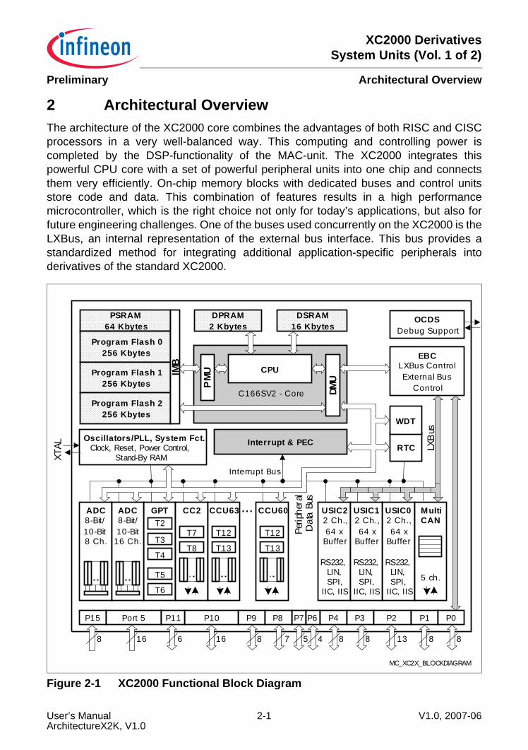
2 Architectural OverviewThe architecture of the XC2000 core combines the advantages of both RISC and CISCprocessors in a very well-balanced way. This computing and controlling power iscompleted by the DSP-functionality of the MAC-unit. The XC2000 integrates thispowerful CPU core with a set of powerful peripheral units into one chip and connectsthem very efficiently. On-chip memory blocks with dedicated buses and control unitsstore code and data. This combination of features results in a high performancemicrocontroller, which is the right choice not only for today’s applications, but also forfuture engineering challenges. One of the buses used concurrently on the XC2000 is theLXBus, an internal representation of the external bus interface. This bus provides astandardized method for integrating additional application-specific peripherals intoderivatives of the standard XC2000.
Figure 2-1 XC2000 Functional Block Diagram
C166SV2 - Core
DPRAM2 Kbytes
CPU
PM
U
DMU
BRGen
ADC8-Bit/10-Bit8 Ch.
USIC02 Ch.,64 x
Buffer
RS232,LIN,SPI,
IIC, IIS
RTC
WDT
Interrupt & PEC
EBCLXBus ControlExternal Bus
Control
DSRAM16 Kbytes
PSRAM64 Kbytes
Oscillators/PLL, System Fct.Clock, Reset, Power Control,
Stand-By RAM
OCDSDebug Support
XTAL
Interrupt Bus
Perip
hera
lD
ata
Bus
8
P15 P9 P7 P6Port 5 P4 P3 P2 P1 P0
888 1384516 8
MC_XC2X_BLOCKDIAGRAM
Program Flash 0256 Kbytes
Program Flash 1256 Kbytes
Program Flash 2256 Kbytes
GPT
T6
T5
T4
T3
T2ADC8-Bit/10-Bit
16 Ch.
CC2
T8
T7
MultiCAN
5 ch.
USIC22 Ch.,64 x
Buffer
RS232,LIN,SPI,
IIC, IIS
USIC12 Ch.,64 x
Buffer
RS232,LIN,SPI,
IIC, IIS
CCU63
T13
T12
CCU60
T13
T12
LXB
us
IMB
P8
7
P10
16
P11
6
...
User’s Manual 2-1 V1.0, 2007-06ArchitectureX2K, V1.0
XC2000 DerivativesSystem Units (Vol. 1 of 2)
Architectural OverviewPreliminary
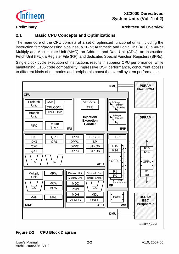
2.1 Basic CPU Concepts and OptimizationsThe main core of the CPU consists of a set of optimized functional units including theinstruction fetch/processing pipelines, a 16-bit Arithmetic and Logic Unit (ALU), a 40-bitMultiply and Accumulate Unit (MAC), an Address and Data Unit (ADU), an InstructionFetch Unit (IFU), a Register File (RF), and dedicated Special Function Registers (SFRs).Single clock cycle execution of instructions results in superior CPU performance, whilemaintaining C166 code compatibility. Impressive DSP performance, concurrent accessto different kinds of memories and peripherals boost the overall system performance.
Figure 2-2 CPU Block Diagram
DPRAM
CPU
IPIP
RFR0R1
GPRs
R14R15
R0R1
GPRs
R14R15
IFU
Injection/ExceptionHandler
ADU
MAC
mca04917_x.vsd
CPUCON1CPUCON2
CSP IP
ReturnStackFIFO
BranchUnit
PrefetchUnit
VECSEG
TFR
+/-
IDX0IDX1QX0QX1
QR0QR1
DPP0DPP1DPP2DPP3
SPSEGSP
STKOVSTKUN
+/-
MRW
MCWMSW
MAL
+/-
MAH
MultiplyUnit
ALU
Division Unit
Multiply Unit
Bit-Mask-Gen.
Barrel-Shifter
+/-MDC
PSW
MDH
ZEROS
MDL
ONES
R0R1
GPRs
R14R15
CP
WB
Buffer
2-StagePrefetch
Pipeline
5-StagePipeline
R0R1
GPRs
R14R15
PMU
DMU
DSRAMEBC
Peripherals
PSRAMFlash/ROM
User’s Manual 2-2 V1.0, 2007-06ArchitectureX2K, V1.0
XC2000 DerivativesSystem Units (Vol. 1 of 2)
Architectural OverviewPreliminary
Summary of CPU Features• Opcode fully upward compatible with C166 Family• 2-stage instruction fetch pipeline with FIFO for instruction pre-fetching• 5-stage instruction execution pipeline• Pipeline forwarding controls data dependencies in hardware• Multiple high bandwidth buses for data and instructions• Linear address space for code and data (von Neumann architecture)• Nearly all instructions executed in one CPU clock cycle• Fast multiplication (16-bit × 16-bit) in one CPU clock cycle• Fast background execution of division (32-bit/16-bit) in 21 CPU clock cycles• Built-in advanced MAC (Multiply Accumulate) Unit:
– Single cycle MAC instruction with zero cycle latency including a 16 × 16 multiplier– 40-bit barrel shifter and 40-bit accumulator to handle overflows– Automatic saturation to 32 bits or rounding included with the MAC instruction– Fractional numbers supported directly– One Finite Impulse Response Filter (FIR) tap per cycle with no circular buffer
management• Enhanced boolean bit manipulation facilities• High performance branch-, call-, and loop-processing• Zero cycle jump execution• Register-based design with multiple variable register banks (byte or word operands)• Two additional fast register banks• Variable stack with automatic stack overflow/underflow detection• “Fast interrupt” and “Fast context switch” featuresThe high performance and flexibility of the CPU is achieved by a number of optimizedfunctional blocks (see Figure 2-2). Optimizations of the functional blocks are describedin detail in the following sections.
User’s Manual 2-3 V1.0, 2007-06ArchitectureX2K, V1.0
XC2000 DerivativesSystem Units (Vol. 1 of 2)
Architectural OverviewPreliminary
2.1.1 High Instruction Bandwidth/Fast ExecutionBased on the hardware provisions, most of the XC2000’s instructions can be executedin just one clock cycle (1/fSYS). This includes arithmetic instructions, logic instructions,and move instructions with most addressing modes.Special instructions such as JMPS take more than one machine cycle. Divideinstructions are mainly executed in the background, so other instructions can beexecuted in parallel. Due to the prediction mechanism (see Section 4.2), correctlypredicted branch instructions require only one cycle or can even be overlaid with anotherinstruction (zero-cycle jump).The instruction cycle time is dramatically reduced through the use of instructionpipelining. This technique allows the core CPU to process portions of multiple sequentialinstruction stages in parallel. Up to seven stages can operate in parallel:The two-stage instruction fetch pipeline fetches and preprocesses instructions fromthe respective program memory:PREFETCH: Instructions are prefetched from the PMU in the predicted order. Theinstructions are preprocessed in the branch detection unit to detect branches. Theprediction logic determines if branches are assumed to be taken or not.FETCH: The instruction pointer for the next instruction to be fetched is calculatedaccording to the branch prediction rules. The branch folding unit preprocesses detectedbranches and combines them with the preceding instructions to enable zero-cyclebranch execution. Prefetched instructions are stored in the instruction FIFO, while storedinstructions are moved from the instruction FIFO to the instruction processing pipeline.The five-stage instruction processing pipeline executes the respective instructions:DECODE: The previously fetched instruction is decoded and the GPR used for indirectaddressing is read from the register file, if required.ADDRESS: All operand addresses are calculated. For instructions implicitly accessingthe stack the stack pointer (SP) is decremented or incremented.MEMORY: All required operands are fetched.EXECUTE: The specified operation (ALU or MAC) is performed on the previouslyfetched operands. The condition flags are updated. Explicit write operations to CPU-SFRs are executed. GPRs used for indirect addressing are incremented ordecremented, if required.WRITE BACK: The result operands are written to the specified locations. Operandslocated in the DPRAM are stored via the write-back buffer.
User’s Manual 2-4 V1.0, 2007-06ArchitectureX2K, V1.0
XC2000 DerivativesSystem Units (Vol. 1 of 2)
Architectural OverviewPreliminary
2.1.2 Powerful Execution UnitsThe 16-bit Arithmetic and Logic Unit (ALU) performs all standard (word) arithmeticand logical operations. Additionally, for byte operations, signals are provided from bits 6and 7 of the ALU result to set the condition flags correctly. Multiple precision arithmeticis provided through a ‘CARRY-IN’ signal to the ALU from previously calculated portionsof the desired operation.Most internal execution blocks have been optimized to perform operations on either 8-bitor 16-bit quantities. Instructions have been provided as well to allow byte packing inmemory while providing sign extension of bytes for word wide arithmetic operations. Theinternal bus structure also allows transfers of bytes or words to or from peripherals basedon the peripheral requirements.A set of consistent flags is updated automatically in the PSW after each arithmetic,logical, shift, or movement operation. These flags allow branching on specific conditions.Support for both signed and unsigned arithmetic is provided through user-specifiablebranch tests. These flags are also preserved automatically by the CPU upon entry intoan interrupt or trap routine.A 16-bit barrel shifter provides multiple bit shifts in a single cycle. Rotates and arithmeticshifts are also supported.The Multiply and Accumulate Unit (MAC) performs extended arithmetic operationssuch as 32-bit addition, 32-bit subtraction, and single-cycle 16-bit × 16-bit multiplication.The combined MAC operations (multiplication with cumulative addition/subtraction)represent the major part of the DSP performance of the CPU.The Address Data Unit (ADU) contains two independent arithmetic units to generate,calculate, and update addresses for data accesses. The ADU performs the followingmajor tasks:• The Standard Address Unit supports linear arithmetic for the short, long, and indirect
addressing modes. It also supports data paging and stack handling.• The DSP Address Generation Unit contains an additional set of address pointers and
offset registers which are used in conjunction with the CoXXX instructions only.The CPU provides a lot of powerful addressing modes for word, byte, and bit dataaccesses (short, long, indirect). The different addressing modes use different formatsand have different scopes.Dedicated bit processing instructions provide efficient control and testing of peripheralswhile enhancing data manipulation. These instructions provide direct access to twooperands in the bit-addressable space without requiring them to be moved intotemporary flags. Logical instructions allow the user to compare and modify a control bitfor a peripheral in one instruction. Multiple bit shift instructions (single cycle execution)avoid long instruction streams of single bit shift operations. Bitfield instructions allow themodification of multiple bits from one operand in a single instruction.
User’s Manual 2-5 V1.0, 2007-06ArchitectureX2K, V1.0
XC2000 DerivativesSystem Units (Vol. 1 of 2)
Architectural OverviewPreliminary
2.1.3 High Performance Branch-, Call-, and Loop-ProcessingPipelined execution delivers maximum performance with a stream of subsequentinstructions. Any disruption requires the pipeline to be refilled and the new instruction tostep through the pipeline stages. Due to the high percentage of branching in controllerapplications, branch instructions have been optimized to require pipeline refilling only inspecial cases. This is realized by detecting and preprocessing branch instructions in theprefetch stage and by predicting the respective branch target address.Prefetching then continues from the predicted target address. If the prediction wascorrect subsequent instructions can be fed to the execution pipeline without a gap, evenif a branch is executed, i.e. the code execution is not linear. Branch target prediction (seealso Section 4.2.1) uses the following rules:• Unconditional branches: Branch prediction is trivial in this case, as the branches will
always be taken and the target address is defined. This applies to implicitlyunconditional branches such as JMPS, CALLR, or RET as well as to branches withcondition code “unconditional” such as JMPI cc_UC.
• Fixed prediction: Branch instructions which are often used to realize loops areassumed to be taken if they branch backward to a previous location (the begin of theloop). This applies to conditional branches such as JMPR cc_XX or JNB.
• Variable prediction: In this case the respective prediction (taken or not taken) iscoded into the instruction and can, therefore, be selected for each individual branchinstruction. Thus, the software designer can optimize the instruction flow to thespecific code to be executed1). This applies to the branch instructions JMPA andCALLA.
• Conditional indirect branches: These branches are always assumed to be nottaken. This applies to branch instructions JMPI cc_XX, [Rw] and CALLI cc_XX, [Rw].
The system state information is saved automatically on the internal system stack, thusavoiding the use of instructions to preserve state upon entry and exit of interrupt or traproutines. Call instructions push the value of the IP on the system stack, and require thesame execution time as branch instructions. Additionally, instructions have beenprovided to support indirect branch and call instructions. This feature supportsimplementation of multiple CASE statement branching in assembler macros and highlevel languages.
1) The programming tools accept either dedicated mnemonics for each prediction leaving the choice up toprogrammer, or they accept generic mnemonics and apply their own prediction rules.
User’s Manual 2-6 V1.0, 2007-06ArchitectureX2K, V1.0

XC2000 DerivativesSystem Units (Vol. 1 of 2)
Architectural OverviewPreliminary
2.1.4 Consistent and Optimized Instruction FormatsTo obtain optimum performance in a pipelined design, an instruction set has beendesigned which incorporates concepts from Reduced Instruction Set Computing (RISC).These concepts primarily allow fast decoding of the instructions and operands whilereducing pipeline holds. These concepts, however, do not preclude the use of complexinstructions required by microcontroller users. The instruction set was designed to meetthe following goals:• Provide powerful instructions for frequently-performed operations which traditionally
have required sequences of instructions. Avoid transfer into and out of temporaryregisters such as accumulators and carry bits. Perform tasks in parallel such as savingstate upon entry into interrupt routines or subroutines.
• Avoid complex encoding schemes by placing operands in consistent fields for eachinstruction and avoid complex addressing modes which are not frequently used.Consequently, the instruction decode time decreases and the development ofcompilers and assemblers is simplified.
• Provide most frequently used instructions with one-word instruction formats. All otherinstructions use two-word formats. This allows all instructions to be placed on wordboundaries: this alleviates the need for complex alignment hardware. It also has thebenefit of increasing the range for relative branching instructions.
The high performance of the CPU-hardware can be utilized efficiently by a programmerby means of the highly functional XC2000 instruction set which includes the followinginstruction classes:• Arithmetic Instructions• DSP Instructions• Logical Instructions• Boolean Bit Manipulation Instructions• Compare and Loop Control Instructions• Shift and Rotate Instructions• Prioritize Instruction• Data Movement Instructions• System Stack Instructions• Jump and Call Instructions• Return Instructions• System Control Instructions• Miscellaneous InstructionsPossible operand types are bits, bytes, words, and doublewords. Specific instructionssupport the conversion (extension) of bytes to words. Various direct, indirect, andimmediate addressing modes are provided to specify the required operands.
User’s Manual 2-7 V1.0, 2007-06ArchitectureX2K, V1.0
XC2000 DerivativesSystem Units (Vol. 1 of 2)
Architectural OverviewPreliminary
2.1.5 Programmable Multiple Priority Interrupt SystemThe XC2000 provides 96 separate interrupt nodes that may be assigned to 16 prioritylevels with 8 group priorities on each level. Most interrupt sources are connected to adedicated interrupt node. In some cases, multi-source interrupt nodes are incorporatedfor efficient use of system resources. These nodes can be activated by several sourcerequests and are controlled via interrupt subnode control registers.The following enhancements within the XC2000 allow processing of a large number ofinterrupt sources:• Peripheral Event Controller (PEC): This processor is used to off-load many interrupt
requests from the CPU. It avoids the overhead of entering and exiting interrupt or traproutines by performing single-cycle interrupt-driven byte or word data transfersbetween any two locations with an optional increment of the PEC source pointer, thedestination pointer, or both. Only one cycle is ‘stolen’ from the current CPU activity toperform a PEC service.
• Multiple Priority Interrupt Controller: This controller allows all interrupts to be assignedany specified priority. Interrupts may also be grouped, which enables the user toprevent similar priority tasks from interrupting each other. For each of the interruptnodes, there is a separate control register which contains an interrupt request flag, aninterrupt enable flag, and an interrupt priority bitfield. After being accepted by the CPU,an interrupt service can be interrupted only by a higher prioritized service request. Forstandard interrupt processing, each of the interrupt nodes has a dedicated vectorlocation.
• Multiple Register Banks: Two local register banks for immediate context switching addto a relocatable global register bank. The user can specify several register bankslocated anywhere in the internal DPRAM and made of up to sixteen general purposeregisters. A single instruction switches from one register bank to another (switchingbanks flushes the pipeline, changing the global bank requires a validation sequence).
The XC2000 is capable of reacting very quickly to non-deterministic events because itsinterrupt response time is within a very narrow range of typically 7 clock cycles (in thecase of internal program execution). Its fast external interrupt inputs are sampled everyclock cycle and allow even very short external signals to be recognized.The XC2000 also provides an excellent mechanism to identify and process exceptionsor error conditions that arise during run-time, so called ‘Hardware Traps’. A hardwaretrap causes an immediate non-maskable system reaction which is similar to a standardinterrupt service (branching to a dedicated vector table location). The occurrence of ahardware trap is additionally signified by an individual bit in the trap flag register (TFR).Unless another, higher prioritized, trap service is in progress, a hardware trap willinterrupt any current program execution. In turn, a hardware trap service can normallynot be interrupted by a standard or PEC interrupt.Software interrupts are supported by means of the ‘TRAP’ instruction in combination withan individual trap (interrupt) number.
User’s Manual 2-8 V1.0, 2007-06ArchitectureX2K, V1.0
XC2000 DerivativesSystem Units (Vol. 1 of 2)
Architectural OverviewPreliminary
2.1.6 Interfaces to System ResourcesThe CPU of the XC2000 interfaces to the system resources via several bus systemswhich contribute to the overall performance by transferring data concurrently. Thisavoids stalling the CPU because instructions or operands need to be transferred.The Dual Port RAM (DPRAM) is directly coupled to the CPU because it houses theglobal register banks. Transfers from/to these locations affect the performance and are,therefore, carefully optimized.The Program Management Unit (PMU) controls accesses to the on-chip programmemory blocks such as the ROM/Flash module and the Program/Data RAM (PSRAM)and also fetches instructions from external memory.The 64-bit interface between the PMU and the CPU delivers the instruction words, whichare requested by the CPU. The PMU decides whether the requested instruction wordhas to be fetched from on-chip memory or from external memory.The Data Management Unit (DMU) controls accesses to the on-chip Data RAM(DSRAM), to the on-chip peripherals connected to the peripheral bus, and to resourceson the external bus. External accesses (including accesses to peripherals connected tothe on-chip LXBus) are executed by the External Bus Controller (EBC).The 16-bit interface between the DMU and the CPU handles all data transfers(operands). Data accesses by the CPU are distributed to the appropriate busesaccording to the defined address map.PMU and DMU are directly coupled to perform cross-over transfers with high speed.Crossover transfers are executed in both directions:• PMU via DMU: Code fetches from external locations are redirected via the DMU to
EBC. Thus, the XC2000 can execute code from external resources. No code can befetched from the Data RAM (DSRAM).
• DMU via PMU: Data accesses can also be executed to on-chip resources controlledby the PMU. This includes the following types of transfers:– Read a constant from the on-chip program ROM/Flash– Read data from the on-chip PSRAM– Write data to the on-chip PSRAM (required prior to executing out of it)– Program/Erase the on-chip Flash memory
User’s Manual 2-9 V1.0, 2007-06ArchitectureX2K, V1.0
XC2000 DerivativesSystem Units (Vol. 1 of 2)
Architectural OverviewPreliminary
2.2 On-Chip System ResourcesThe XC2000 controllers provide a number of powerful system resources designedaround the CPU. The combination of CPU and these resources results in the highperformance of the members of this controller family.
Peripheral Event Controller (PEC) and Interrupt ControlThe Peripheral Event Controller enables response to an interrupt request with a singledata transfer (word or byte) which consumes only one instruction cycle and does notrequire saving and restoring the machine status. Each interrupt source is prioritized forevery machine cycle in the interrupt control block. If PEC service is selected, a PECtransfer is started. If CPU interrupt service is requested, the current CPU priority levelstored in the PSW register is tested to determine whether a higher priority interrupt iscurrently being serviced. When an interrupt is acknowledged, the current state of themachine is saved on the internal system stack and the CPU branches to the systemspecific vector for the peripheral.The PEC contains a set of SFRs which store the count value and control bits for eightdata transfer channels. In addition, the PEC uses a dedicated area of RAM whichcontains the source and destination addresses. The PEC is controlled in a mannersimilar to any other peripheral: through SFRs containing the desired configuration ofeach channel.An individual PEC transfer counter is implicitly decremented for each PEC serviceexcept in the continuous transfer mode. When this counter reaches zero, a standardinterrupt is performed to the vector location related to the corresponding source. PECservices are very well suited, for example, to moving register contents to/from a memorytable. The XC2000 has eight PEC channels, each of which offers such fast interrupt-driven data transfer capabilities.
Memory AreasThe memory space of the XC2000 is configured in a Von Neumann architecture. Thismeans that code memory, data memory, registers, and IO ports are organized within thesame linear address space which covers up to 16 Mbytes. The entire memory space canbe accessed bytewise or wordwise. Particular portions of the on-chip memory have beenmade directly bit addressable as well.Note: The actual memory sizes depend on the selected device type. This overview
describes the maximum block sizes.
768 Kbytes of on-chip Flash memory store code or constant data. The on-chip Flashmemory consists of 3 Flash modules, each organized as 64 4-Kbyte sectors. Eachsector can be separately write protected1), erased and programmed (in blocks of 128bytes). The complete Flash area can be read-protected. A user-defined passwordsequence temporarily unlocks protected areas. The Flash modules combine 128-bit
User’s Manual 2-10 V1.0, 2007-06ArchitectureX2K, V1.0
XC2000 DerivativesSystem Units (Vol. 1 of 2)
Architectural OverviewPreliminary
read accesses with protected and efficient writing algorithms for programming anderasing. Dynamic error correction provides extremely high read data security for all readaccesses. Accesses to different Flash modules can be executed in parallel.Note: Program execution from on-chip program memory is the fastest of all possible
alternatives and results in maximum performance. The type of the on-chipprogram memory depends on the chosen derivative. On-chip program memoryalso includes the PSRAM.
64 Kbytes of on-chip Program SRAM (PSRAM) are provided to store user code ordata. The PSRAM is accessed via the PMU and is, therefore, optimized for code fetches.A section of the PSRAM with programmable size can be write-protected.16 Kbytes of on-chip Data SRAM (DSRAM) are provided as a storage for general userdata. The DSRAM is accessed via a separate interface and is, therefore, optimized fordata accesses.2 Kbytes of on-chip Dual-Port RAM (DPRAM) are provided as a storage for userdefined variables, for the system stack, and in particular for general purpose registerbanks. A register bank can consist of up to 16 wordwide (R0 to R15) and/or bytewide(RL0, RH0, …, RL7, RH7) so-called General Purpose Registers (GPRs).The upper 256 bytes of the DPRAM are directly bitaddressable. When used by a GPR,any location in the DPRAM is bitaddressable.1 Kbyte of on-chip Stand-By SRAM (SBRAM) is provided as a storage for system-relevant user data that must be preserved while the major part of the device is powereddown. The SBRAM is accessed via a specific interface and is powered via domain M.The CPU has an actual register context of up to 16 wordwide and/or bytewide globalGPRs at its disposal, which are physically located within the on-chip RAM area. AContext Pointer (CP) register determines the base address of the active global registerbank to be accessed by the CPU at a time. The number of register banks is restrictedonly by the available internal RAM space. For easy parameter passing, a register bankmay overlap other register banks.A system stack of up to 32 Kwords is provided as storage for temporary data. The systemstack can be located anywhere within the complete addressing range and it is accessedby the CPU via the Stack Pointer (SP) register and the Stack Pointer Segment (SPSEG)register. Two separate SFRs, STKOV and STKUN, are implicitly compared against thestack pointer value upon each stack access for the detection of a stack overflow orunderflow. This mechanism also supports the control of a bigger virtual stack. Maximumperformance for stack operations is achieved by allocating the system stack to internaldata RAM areas (DPRAM, DSRAM).
1) To save control bits, sectors are clustered for protection purposes, they remain separate for programming/erasing.
User’s Manual 2-11 V1.0, 2007-06ArchitectureX2K, V1.0
XC2000 DerivativesSystem Units (Vol. 1 of 2)
Architectural OverviewPreliminary
Hardware detection of the selected memory space is placed at the internal memorydecoders and allows the user to specify any address directly or indirectly and obtain thedesired data without using temporary registers or special instructions.For Special Function Registers three areas of the address space are reserved: Thestandard Special Function Register area (SFR) uses 512 bytes, while the ExtendedSpecial Function Register area (ESFR) uses the other 512 bytes. A range of 4 Kbytes isprovided for the internal IO area (XSFR). SFRs are wordwide registers which are usedfor controlling and monitoring functions of the different on-chip units. Unused SFRaddresses are reserved for future members of the XC2000 Family with enhancedfunctionality. Therefore, they should either not be accessed, or written with zeros, toensure upward compatibility.In order to meet the needs of designs where more memory is required than is providedon chip, up to 12 Mbytes (approximately, see Table 2-1) of external RAM and/or ROMcan be connected to the microcontroller. The External Bus Interface also providesaccess to external peripherals.
Table 2-1 XC2000 Memory MapAddress Area Start Loc. End Loc. Area Size1) NotesIMB register space FF’FF00H FF’FFFFH 256 Bytes –Reserved (Access trap) F0’0000H FF’FEFFH <1 Mbyte Minus IMB reg.Reserved for EPSRAM E9’0000H EF’FFFFH 448 Kbytes Mirrors EPSRAMEmulated PSRAM E8’0000H E8’FFFFH 64 Kbytes Flash timingReserved for PSRAM E1’0000H E7’FFFFH 448 Kbytes Mirrors PSRAMProgram SRAM E0’0000H E0’FFFFH 64 Kbytes Maximum speedReserved for pr. mem. CC’0000H DF’FFFFH <1.25 Mbytes –Program Flash 2 C8’0000H CB’FFFFH 256 Kbytes –Program Flash 1 C4’0000H C7’FFFFH 256 Kbytes –Reserved Sector (PF0) C3’F000H C3’FFFFH 4 Kbytes Used internallyProgram Flash 0 C0’0000H C3’EFFFH 252 Kbytes –External memory area 40’0000H BF’FFFFH 8 Mbytes –Available Ext. IO area2) 20’5800H 3F’FFFFH < 2 Mbytes Minus USIC/CANUSIC registers 20’4000H 20’57FFH 6 Kbytes Accessed via EBCMultiCAN registers 20’0000H 20’3FFFH 16 Kbytes Accessed via EBCExternal memory area 01’0000H 1F’FFFFH < 2 Mbytes Minus segment 0SFR area 00’FE00H 00’FFFFH 0.5 Kbyte –Dual-Port RAM 00’F600H 00’FDFFH 2 Kbytes –
User’s Manual 2-12 V1.0, 2007-06ArchitectureX2K, V1.0
XC2000 DerivativesSystem Units (Vol. 1 of 2)
Architectural OverviewPreliminary
Note: For an overview of the available memory sections for the different derivatives,please refer to Table 1-1 "XC2000 Derivative Synopsis" on Page 1-2.
Reserved for DPRAM 00’F200H 00’F5FFH 1 Kbyte –ESFR area 00’F000H 00’F1FFH 0.5 Kbyte –XSFR area 00’E000H 00’EFFFH 4 Kbytes –Data SRAM 00’A000H 00’DFFFH 16 Kbytes –Reserved for DSRAM 00’8000H 00’9FFFH 8 Kbytes –External memory area 00’0000H 00’7FFFH 32 Kbytes –1) The areas marked with “<” are slightly smaller than indicated, see column “Notes”.2) Several pipeline optimizations are not active within the external IO area. This is necessary to control external
peripherals properly.
Table 2-1 XC2000 Memory Map (cont’d)
Address Area Start Loc. End Loc. Area Size1) Notes
User’s Manual 2-13 V1.0, 2007-06ArchitectureX2K, V1.0
XC2000 DerivativesSystem Units (Vol. 1 of 2)
Architectural OverviewPreliminary
External Bus InterfaceTo meet the needs of designs where more memory is required than is provided on chip,up to 12 Mbytes of external RAM/ROM/Flash or peripherals can be connected to theXC2000 microcontroller via its external bus interface.All of the external memory accesses are performed by a particular on-chip External BusController (EBC). It can be programmed either to Single Chip Mode when no externalmemory is required, or to an external bus mode with the following possible selections1):• Address Bus Width with a range of 0 … 24-bit• Data Bus Width 8-bit or 16-bit• Bus Operation Multiplexed or DemultiplexedIn the demultiplexed bus modes, addresses are output on Port 0 and Port 1 and data isinput/output on Port 10 and Port 2. In the multiplexed bus modes both addresses anddata use Port 10 and Port 2 for input/output. The high order address (segment) lines usePort 2. The number of active segment address lines is selectable, restricting the externaladdress space to 8 Mbytes … 64 Kbytes. This is required when interface lines areassigned to Port 2.For up to five address areas the bus mode (multiplexed/demultiplexed), the data buswidth (8-bit/16-bit) and even the length of a bus cycle (waitstates, signal delays) can beselected independently. This allows access to a variety of memory and peripheralcomponents directly and with maximum efficiency.Access to very slow memories or modules with varying access times is supported via aparticular ‘Ready’ function. The active level of the control input signal is selectable.A HOLD/HLDA protocol is available for bus arbitration and allows the sharing of externalresources with other bus masters.The external bus timing is related to the rising edge of the reference clock outputCLKOUT. The external bus protocol is compatible with that of the standard C166 Family.For applications which require less than 64 Kbytes of address space, a non-segmentedmemory model can be selected, where all locations can be addressed by 16 bits. Thus,the upper Port 2 is not needed as an output for the upper address bits (Axx … A16), asis the case when using the segmented memory model.The EBC also controls accesses to resources connected to the on-chip LXBus. TheLXBus is an internal representation of the external bus and allows accessing integratedperipherals and modules in the same way as external components.The MultiCAN module and the USIC modules are connected to and accessed via theLXBus.
1) Bus modes are switched dynamically if several address windows with different mode settings are used.
User’s Manual 2-14 V1.0, 2007-06ArchitectureX2K, V1.0
XC2000 DerivativesSystem Units (Vol. 1 of 2)
Architectural OverviewPreliminary
2.3 On-Chip Peripheral BlocksThe XC2000 Family clearly separates peripherals from the core. This structure permitsthe maximum number of operations to be performed in parallel and allows peripherals tobe added or deleted from family members without modifications to the core. Eachfunctional block processes data independently and communicates information overcommon buses. Peripherals are controlled by data written to the respective SpecialFunction Registers (SFRs). These SFRs are located within either the standard SFR area(00’FE00H … 00’FFFFH), the extended ESFR area (00’F000H … 00’F1FFH), or withinthe internal IO area (00’E000H … 00’EFFFH).These built-in peripherals either allow the CPU to interface with the external world orprovide functions on-chip that otherwise would need to be added externally in therespective system.The XC2000 generic peripherals are:• Two General Purpose Timer Blocks (GPT1 and GPT2)• A Watchdog Timer• A Capture/Compare unit (CAPCOM2)• Up to Four Enhanced Capture/Compare units (CCU60, CCU61, CCU62, CCU63)• Two 10-bit Analog/Digital Converters (ADC0, ADC1)• A Real Time Clock (RTC)• Thirteen I/O ports with a total of 118(75) I/O linesBecause the LXBus is the internal representation of the external bus, it does not supportbit-addressing. Accesses are executed by the EBC as if it were external accesses. TheLXBus connects on-chip peripherals to the CPU:• MultiCAN module with up to 5 CAN nodes and gateway functionality• Three Serial Interface Modules providing six serial channelsEach peripheral also contains a set of Special Function Registers (SFRs) which controlthe functionality of the peripheral and temporarily store intermediate data results. Eachperipheral has an associated set of status flags. Individually selected clock signals aregenerated for each peripheral from binary multiples of the master clock.Note: For an overview of the available peripherals for the different derivatives, please
refer to Table 1-1 "XC2000 Derivative Synopsis" on Page 1-2.
User’s Manual 2-15 V1.0, 2007-06ArchitectureX2K, V1.0
XC2000 DerivativesSystem Units (Vol. 1 of 2)
Architectural OverviewPreliminary
Peripheral InterfacesThe on-chip peripherals generally have two different types of interfaces: an interface tothe CPU and an interface to external hardware. Communication between the CPU andperipherals is performed through Special Function Registers (SFRs) and interrupts. TheSFRs serve as control/status and data registers for the peripherals. Interrupt requestsare generated by the peripherals based on specific events which occur during theiroperation, such as operation complete, error, etc.To interface with external hardware, specific pins of the parallel ports are used, when aninput or output function has been selected for a peripheral. During this time, the port pinsare controlled either by the peripheral (when used as outputs) or by the externalhardware which controls the peripheral (when used as inputs). This is called the‘alternate (input or output) function’ of a port pin, in contrast to its function as a generalpurpose I/O pin.
Peripheral TimingInternal operation of the CPU and peripherals is based on the master clock (fMC). Theclock generation unit uses the on-chip oscillator to derive the master clock from thecrystal or from the external clock signal. The clock signal gated to the peripherals isindependent from the clock signal that feeds the CPU. During Idle mode, the CPU’s clockis stopped while the peripherals continue their operation. Peripheral SFRs may beaccessed by the CPU once per state. When an SFR is written to by software in the samestate where it is also to be modified by the peripheral, the software write operation haspriority. Further details on peripheral timing are included in the specific sectionsdescribing each peripheral.
Programming Hints• Access to SFRs: All SFRs reside in data page 3 of the memory space. The following
addressing mechanisms allow access to the SFRs:– Indirect or direct addressing with 16-bit (mem) addresses must guarantee that the
used data page pointer (DPP0 … DPP3) selects data page 3.– Accesses via the Peripheral Event Controller (PEC) use the SRCPx and DSTPx
pointers instead of the data page pointers.– Short 8-bit (reg) addresses to the standard SFR area do not use the data page
pointers but directly access the registers within this 512-byte area.– Short 8-bit (reg) addresses to the extended ESFR area require switching to the
512-byte Extended SFR area. This is done via the EXTension instructions EXTR,EXTP(R), EXTS(R).
• Byte Write Operations to wordwide SFRs via indirect or direct 16-bit (mem)addressing or byte transfers via the PEC force zeros in the non-addressed byte. Bytewrite operations via short 8-bit (reg) addressing can access only the low byte of anSFR and force zeros in the high byte. It is therefore recommended, to use the bitfield
User’s Manual 2-16 V1.0, 2007-06ArchitectureX2K, V1.0

XC2000 DerivativesSystem Units (Vol. 1 of 2)
Architectural OverviewPreliminary
instructions (BFLDL and BFLDH) to write to any number of bits in either byte of anSFR without disturbing the non-addressed byte and the unselected bits.
• Reserved Bits: Some of the bits which are contained in the XC2000’s SFRs aremarked as ‘Reserved’. User software should never write ‘1’s to reserved bits. Thesebits are currently not implemented and may be used in future products to invoke newfunctions. In that case, the active state for those new functions will be ‘1’, and theinactive state will be ‘0’. Therefore writing only ‘0’s to reserved locations allowsportability of the current software to future devices. After read accesses, reserved bitsshould be ignored or masked out.
Capture/Compare Unit (CAPCOM2)The CAPCOM units support generation and control of timing sequences on up to16 channels with a maximum resolution of 1 system clock cycle (8 cycles in staggeredmode). The CAPCOM unit is typically used to handle high speed I/O tasks such as pulseand waveform generation, pulse width modulation (PMW), Digital to Analog (D/A)conversion, software timing, or time recording relative to external events.Two 16-bit timers (T7/T8) with reload registers provide two independent time bases foreach capture/compare register.The input clock for the timers is programmable to several prescaled values of the internalsystem clock, or may be derived from an overflow/underflow of timer T6 in module GPT2.This provides a wide range of variation for the timer period and resolution and allowsprecise adjustments to the application specific requirements. In addition, external countinputs for CAPCOM timer T7 allow event scheduling for the capture/compare registersrelative to external events.The capture/compare register array contains 16 dual purpose capture/compareregisters, each of which may be individually allocated to either CAPCOM timer T7 or T8and programmed for capture or compare function.All registers of each module have each one port pin associated with it which serves asan input pin for triggering the capture function, or as an output pin to indicate theoccurrence of a compare event.
User’s Manual 2-17 V1.0, 2007-06ArchitectureX2K, V1.0
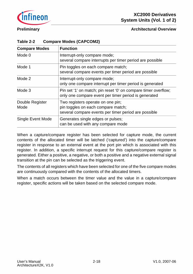
XC2000 DerivativesSystem Units (Vol. 1 of 2)
Architectural OverviewPreliminary
When a capture/compare register has been selected for capture mode, the currentcontents of the allocated timer will be latched (‘captured’) into the capture/compareregister in response to an external event at the port pin which is associated with thisregister. In addition, a specific interrupt request for this capture/compare register isgenerated. Either a positive, a negative, or both a positive and a negative external signaltransition at the pin can be selected as the triggering event.The contents of all registers which have been selected for one of the five compare modesare continuously compared with the contents of the allocated timers.When a match occurs between the timer value and the value in a capture/compareregister, specific actions will be taken based on the selected compare mode.
Table 2-2 Compare Modes (CAPCOM2)Compare Modes FunctionMode 0 Interrupt-only compare mode;
several compare interrupts per timer period are possibleMode 1 Pin toggles on each compare match;
several compare events per timer period are possibleMode 2 Interrupt-only compare mode;
only one compare interrupt per timer period is generatedMode 3 Pin set ‘1’ on match; pin reset ‘0’ on compare timer overflow;
only one compare event per timer period is generatedDouble Register Mode
Two registers operate on one pin;pin toggles on each compare match;several compare events per timer period are possible
Single Event Mode Generates single edges or pulses;can be used with any compare mode
User’s Manual 2-18 V1.0, 2007-06ArchitectureX2K, V1.0
XC2000 DerivativesSystem Units (Vol. 1 of 2)
Architectural OverviewPreliminary
Capture/Compare Units CCU6 The CCU6 units support generation and control of timing sequences on up to three 16-bit capture/compare channels plus one independent 16-bit compare channel.In compare mode, the CCU6 units provide two output signals per channel which haveinverted polarity and non-overlapping pulse transitions (deadtime control). The comparechannel can generate a single PWM output signal and is further used to modulate thecapture/compare output signals.In capture mode the contents of compare timer T12 is stored in the capture registersupon a signal transition at pins CCx.The output signals can be generated in edge-aligned or center-aligned PWM mode.They are generated continuously or in single-shot mode.Compare timers T12 and T13 are free running timers which are clocked by the prescaledsystem clock.For motor control applications (brushless DC-drives) both subunits may generateversatile multichannel PWM signals which are basically either controlled by comparetimer T12 or by a typical hall sensor pattern at the interrupt inputs (block commutation).The latter mode provides noise filtering for the hall inputs and supports automaticrotational speed measurement.The trap function offers a fast emergency stop without CPU activity. Triggered by anexternal signal (CTRAP) the outputs are switched to selectable logic levels which can beadapted to the connected power stages.Note: The number of available CCU6 units and channels depends on the selected
device type.
User’s Manual 2-19 V1.0, 2007-06ArchitectureX2K, V1.0
XC2000 DerivativesSystem Units (Vol. 1 of 2)
Architectural OverviewPreliminary
General Purpose Timer (GPT12E) UnitThe GPT12E unit represents a very flexible multifunctional timer/counter structure whichmay be used for many different time related tasks such as event timing and counting,pulse width and duty cycle measurements, pulse generation, or pulse multiplication.The GPT12E unit incorporates five 16-bit timers which are organized in two separateblocks, GPT1 and GPT2. Each timer in each block may operate independently in anumber of different modes, or may be concatenated with another timer of the sameblock.Each of the three timers T2, T3, T4 of block GPT1 can be configured individually for oneof four basic modes of operation, which are Timer, Gated Timer, Counter, andIncremental Interface Mode. In Timer Mode, the input clock for a timer is derived fromthe system clock, divided by a programmable prescaler, while Counter Mode allows atimer to be clocked in reference to external events.Pulse width or duty cycle measurement is supported in Gated Timer Mode, where theoperation of a timer is controlled by the ‘gate’ level on an external input pin. For thesepurposes, each timer has one associated port pin (TxIN) which serves as gate or clockinput. The maximum resolution of the timers in block GPT1 is 4 system clock cycles.The count direction (up/down) for each timer is programmable by software or mayadditionally be altered dynamically by an external signal on a port pin (TxEUD) tofacilitate e.g. position tracking.In Incremental Interface Mode the GPT1 timers (T2, T3, T4) can be directly connectedto the incremental position sensor signals A and B via their respective inputs TxIN andTxEUD. Direction and count signals are internally derived from these two input signals,so the contents of the respective timer Tx corresponds to the sensor position. The thirdposition sensor signal TOP0 can be connected to an interrupt input.Timer T3 has an output toggle latch (T3OTL) which changes its state on each timer over-flow/underflow. The state of this latch may be output on pin T3OUT e.g. for time outmonitoring of external hardware components. It may also be used internally to clocktimers T2 and T4 for measuring long time periods with high resolution.In addition to their basic operating modes, timers T2 and T4 may be configured as reloador capture registers for timer T3. When used as capture or reload registers, timers T2and T4 are stopped. The contents of timer T3 is captured into T2 or T4 in response to asignal at their associated input pins (TxIN). Timer T3 is reloaded with the contents of T2or T4 triggered either by an external signal or by a selectable state transition of its togglelatch T3OTL. When both T2 and T4 are configured to alternately reload T3 on oppositestate transitions of T3OTL with the low and high times of a PWM signal, this signal canbe constantly generated without software intervention.With its maximum resolution of 2 system clock cycles, the GPT2 block provides preciseevent control and time measurement. It includes two timers (T5, T6) and a capture/reload register (CAPREL). Both timers can be clocked with an input clock which is
User’s Manual 2-20 V1.0, 2007-06ArchitectureX2K, V1.0
XC2000 DerivativesSystem Units (Vol. 1 of 2)
Architectural OverviewPreliminary
derived from the CPU clock via a programmable prescaler or with external signals. Thecount direction (up/down) for each timer is programmable by software or mayadditionally be altered dynamically by an external signal on a port pin (TxEUD).Concatenation of the timers is supported via the output toggle latch (T6OTL) of timer T6,which changes its state on each timer overflow/underflow.The state of this latch may be used to clock timer T5, and/or it may be output on pinT6OUT. The overflows/underflows of timer T6 can additionally be used to clock theCAPCOM1/2 timers, and to cause a reload from the CAPREL register.The CAPREL register may capture the contents of timer T5 based on an external signaltransition on the corresponding port pin (CAPIN), and timer T5 may optionally be clearedafter the capture procedure. This allows the XC2000 to measure absolute timedifferences or to perform pulse multiplication without software overhead.The capture trigger (timer T5 to CAPREL) may also be generated upon transitions ofGPT1 timer T3’s inputs T3IN and/or T3EUD. This is especially advantageous when T3operates in Incremental Interface Mode.
User’s Manual 2-21 V1.0, 2007-06ArchitectureX2K, V1.0
XC2000 DerivativesSystem Units (Vol. 1 of 2)
Architectural OverviewPreliminary
Real Time ClockThe Real Time Clock (RTC) module of the XC2000 is directly clocked via a separateclock driver either with the on-chip auxiliary oscillator frequency (fRTC = fOSCa) or with theprescaled on-chip main oscillator frequency (fRTC = fOSCm/32). It is thereforeindependent from the selected clock generation mode of the XC2000.The RTC basically consists of a chain of divider blocks:• Selectable 32:1 and 8:1 dividers (on - off)• The reloadable 16-bit timer T14• The 32-bit RTC timer block (accessible via registers RTCH and RTCL), made of:
– a reloadable 10-bit timer– a reloadable 6-bit timer– a reloadable 6-bit timer– a reloadable 10-bit timer
All timers count up. Each timer can generate an interrupt request. All requests arecombined to a common node request.Note: The registers associated with the RTC are not affected by a functional reset in
order to maintain the contents even when intermediate resets are executed.
The RTC module can be used for different purposes:• System clock to determine the current time and date• Cyclic time based interrupt, to provide a system time tick independent of CPU
frequency and other resources• 48-bit timer for long term measurements• Alarm interrupt for wake-up on a defined time
User’s Manual 2-22 V1.0, 2007-06ArchitectureX2K, V1.0
XC2000 DerivativesSystem Units (Vol. 1 of 2)
Architectural OverviewPreliminary
A/D ConvertersFor analog signal measurement, two 10-bit A/D converters (ADC0, ADC1) with 16 (or 8)multiplexed input channels including a sample and hold circuit have been integrated on-chip. They use the method of successive approximation. The sample time (for loadingthe capacitors) and the conversion time are programmable and can thus be adjusted tothe external circuitry. The A/D converters can also operate in 8-bit conversion mode,where the conversion time is further reduced.Several independent conversion result registers, selectable interrupt requests, andhighly flexible conversion sequences provide a high degree of programmability to fulfillthe requirements of the respective application. Both modules can be synchronized toallow parallel sampling of two input channels.For applications that require more analog input channels, external analog multiplexerscan be controlled automatically.For applications that require less analog input channels, the remaining channel inputscan be used as digital input port pins.The A/D converters of the XC2000 support two types of request sources which can betriggered by several internal and external events.• Parallel requests are activated at the same time and then executed in a predefined
sequence.• Queued requests are executed in a user-defined sequence.In addition, the conversion of a specific channel can be inserted into a running sequencewithout disturbing this sequence. All requests are arbitrated according to the priority levelthat has been assigned to them.Data reduction features, such as limit checking or result accumulation, reduce thenumber of required CPU accesses and so allow the precise evaluation of analog inputs(high conversion rate) even at low CPU speed.The Peripheral Event Controller (PEC) may be used to control the A/D converters or toautomatically store conversion results into a table in memory for later evaluation, withoutrequiring the overhead of entering and exiting interrupt routines for each data transfer.Therefore, each A/D converter contains 8 result registers which can be concatenated tobuild a result FIFO. Wait-for-read mode can be enabled for each result register toprevent loss of conversion data.In order to decouple analog inputs from digital noise and to avoid input trigger noisethose pins used for analog input can be disconnected from the digital input stages undersoftware control. This can be selected for each pin separately via registers P5_DIDISand P15_DIDIS (Port x Digital Input Disable).The Auto-Power-Down feature of the A/D converters minimizes the power consumptionwhen no conversion is in progress.Note: The number of available analog channels depends on the selected device type.
User’s Manual 2-23 V1.0, 2007-06ArchitectureX2K, V1.0
XC2000 DerivativesSystem Units (Vol. 1 of 2)
Architectural OverviewPreliminary
Universal Serial Interface Channel Modules (USIC)Each USIC channel can be individually configured to match the application needs, e.g.the protocol can be selected or changed during run time without the need for a reset. Thefollowing protocols are supported:• UART (ASC, asynchronous serial channel)
- module capability: receiver/transmitter with max. baud rate fsys/4- application target baud rate range: 1.2 kBaud to 3.5 MBaud- number of data bits per data frame 1 to 63- MSB or LSB first
• LIN Support by HW (low-cost network, baud rate up to 20 kBaud)- data transfers based on ASC protocol- baud rate detection possible by built-in capture event of baud rate generator- checksum generation under SW control for higher flexibility
• SSC/SPI (synchronous serial channel with or without slave select lines)- module capability: slave mode with max. baud rate fsys- module capability: master mode with max. baud rate fsys /2- application target baud rate range: 2 kBaud to 10 MBaud- number of data bits per data frame 1 to 63, more with explicit stop condition- MSB or LSB first
• IIC (Inter-IC Bus)- application baud rate 100 kBaud to 400 kBaud- 7-bit and 10-bit addressing supported- full master and slave device capability
• IIS (infotainment audio bus)- module capability: receiver with max. baud rate fSYS- module capability: transmitter with max. baud rate fSYS /2- application target baud rate range: up to 26 MBaud
In addition to the flexible choice of the communication protocol, the USIC structure hasbeen designed to reduce the system load (CPU load) allowing efficient data handling.The following aspects have been considered:• Data buffer capability
The standard buffer capability includes a double word buffer for receive data and asingle word buffer for transmit data. This allows longer CPU reaction times (e.g.interrupt latency).
• Additional FIFO buffer capabilityIn addition to the standard buffer capability, the received data and the data to betransmitted can be buffered in a FIFO buffer structure. The size of the receive and thetransmit FIFO buffer can be programmed independently. Depending on theapplication needs, a total buffer capability of 64 data words can be assigned to thereceive and transmit FIFO buffers of a USIC module (the two channels of the USICmodule share the 64 data word buffer).
User’s Manual 2-24 V1.0, 2007-06ArchitectureX2K, V1.0
XC2000 DerivativesSystem Units (Vol. 1 of 2)
Architectural OverviewPreliminary
In addition to the FIFO buffer, a bypass mechanism allows the introduction of high-priority data without flushing the FIFO buffer.
• Transmit control informationFor each data word to be transmitted, a 5-bit transmit control information has beenadded to automatically control some transmission parameters, such as word length,frame length, or the slave select control for the SPI protocol. The transmit controlinformation is generated automatically by analyzing the address where the user SWhas written the data word to be transmitted (32 input locations = 2^5 = 5 bit transmitcontrol information).This feature allows individual handling of each data word, e.g. the transmit controlinformation associated to the data words stored in a transmit FIFO can automaticallymodify the slave select outputs to select different communication targets (slavedevices) without CPU load. Alternatively, it can be used to control the frame length.
• Flexible frame length controlThe number of bits to be transferred within a data frame is independent of the dataword length and can be handled in two different ways. The first option allowsautomatic generation of frames up to 63 bits with a known length. The second optionsupports longer frames (even unlimited length) or frames with a dynamically controlledlength.
• Interrupt capabilityThe events of each USIC channel can be individually routed to one of 4 servicerequest outputs, depending on the application needs. Furthermore, specific start andend of frame indications are supported in addition to protocol-specific events.
• Flexible interface routingEach USIC channel offers the choice between several possible input and output pinsconnections for the communications signals. This allows a flexible assignment ofUSIC signals to pins that can be changed without resetting the device.
• Input conditioningEach input signal is handled by a programmable input conditioning stage withprogrammable filtering and synchronization capability.
• Baud rate generationEach USIC channel contains an own baud rate generator. The baud rate generationcan be based either on the internal module clock or on an external frequency input.This structure allows data transfers with a frequency that can not be generatedinternally, e.g. to synchronize several communication partners.
• Transfer trigger capabilityIn master mode, data transfers can be triggered events generated outside the USICmodule, e.g. at an input pin or a timer unit (transmit data validation). This featureallows time base related data transmission.
• Debugger supportThe USIC offers specific addresses to read out received data without interaction withthe FIFO buffer mechanism. This feature allows debugger accesses without the riskof a corrupted receive data sequence.
User’s Manual 2-25 V1.0, 2007-06ArchitectureX2K, V1.0
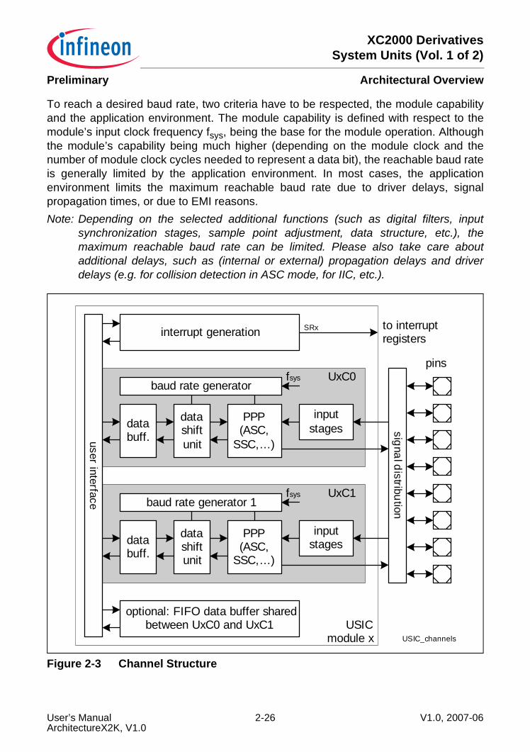
XC2000 DerivativesSystem Units (Vol. 1 of 2)
Architectural OverviewPreliminary
To reach a desired baud rate, two criteria have to be respected, the module capabilityand the application environment. The module capability is defined with respect to themodule’s input clock frequency fsys, being the base for the module operation. Althoughthe module’s capability being much higher (depending on the module clock and thenumber of module clock cycles needed to represent a data bit), the reachable baud rateis generally limited by the application environment. In most cases, the applicationenvironment limits the maximum reachable baud rate due to driver delays, signalpropagation times, or due to EMI reasons.Note: Depending on the selected additional functions (such as digital filters, input
synchronization stages, sample point adjustment, data structure, etc.), themaximum reachable baud rate can be limited. Please also take care aboutadditional delays, such as (internal or external) propagation delays and driverdelays (e.g. for collision detection in ASC mode, for IIC, etc.).
Figure 2-3 Channel Structure
UxC1
USIC_channels
user interface
databuff.
baud rate generator 1
datashiftunit
PPP(ASC,
SSC,…)
signal distribution
pins
fsys
inputstages
databuff.
baud rate generator
datashiftunit
PPP(ASC,
SSC,…)
fsys
inputstages
UxC0
optional: FIFO data buffer sharedbetween UxC0 and UxC1 USIC
module x
interrupt generation SRx to interruptregisters
User’s Manual 2-26 V1.0, 2007-06ArchitectureX2K, V1.0
XC2000 DerivativesSystem Units (Vol. 1 of 2)
Architectural OverviewPreliminary
The USIC module contains two independent communication channels, with structureshown in Figure 2-3.The data shift unit and the data buffering of each channel support full-duplex datatransfers. The protocol-specific actions are handled by protocol pre-processors (PPP).In order to simplify data handling, an additional FIFO data buffer is optionally availablefor each USIC module to store transmit and receive data for each channel. This FIFOdata buffer is not necessarily available in all devices (please refer to USICimplementation chapter for details).Due to the independent channel control and baud rate generation, the communicationprotocol, baud rate and the data format can be independently programmed for eachcommunication channel.
User’s Manual 2-27 V1.0, 2007-06ArchitectureX2K, V1.0
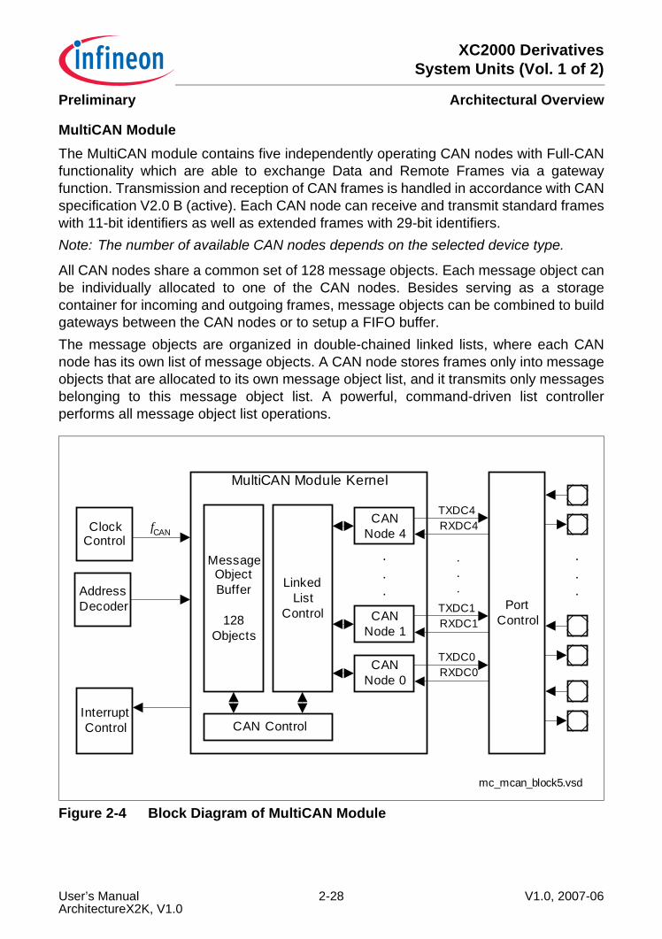
XC2000 DerivativesSystem Units (Vol. 1 of 2)
Architectural OverviewPreliminary
MultiCAN ModuleThe MultiCAN module contains five independently operating CAN nodes with Full-CANfunctionality which are able to exchange Data and Remote Frames via a gatewayfunction. Transmission and reception of CAN frames is handled in accordance with CANspecification V2.0 B (active). Each CAN node can receive and transmit standard frameswith 11-bit identifiers as well as extended frames with 29-bit identifiers.Note: The number of available CAN nodes depends on the selected device type.
All CAN nodes share a common set of 128 message objects. Each message object canbe individually allocated to one of the CAN nodes. Besides serving as a storagecontainer for incoming and outgoing frames, message objects can be combined to buildgateways between the CAN nodes or to setup a FIFO buffer.The message objects are organized in double-chained linked lists, where each CANnode has its own list of message objects. A CAN node stores frames only into messageobjects that are allocated to its own message object list, and it transmits only messagesbelonging to this message object list. A powerful, command-driven list controllerperforms all message object list operations.
Figure 2-4 Block Diagram of MultiCAN Module
mc_mcan_block5.vsd
MultiCAN Module Kernel
InterruptControl
fCAN
PortControlCAN
Node 1
CAN Control
MessageObjectBuffer
128Objects
CANNode 0
LinkedList
Control
ClockControl
AddressDecoder
CANNode 4
TXDC4RXDC4
TXDC1RXDC1
TXDC0RXDC0
.
.
.
.
.
.
.
.
.
User’s Manual 2-28 V1.0, 2007-06ArchitectureX2K, V1.0
XC2000 DerivativesSystem Units (Vol. 1 of 2)
Architectural OverviewPreliminary
MultiCAN Features• CAN functionality conforms to CAN specification V2.0 B active for each CAN node
(compliant to ISO 11898)• Up to Five independent CAN nodes• Up to 128 independent message objects (shared by the CAN nodes)• Dedicated control registers for each CAN node• Data transfer rate up to 1 Mbit/s, individually programmable for each node• Flexible and powerful message transfer control and error handling capabilities• Full-CAN functionality for message objects:
– Can be assigned to one of the CAN nodes– Configurable as transmit or receive objects, or as message buffer FIFO– Handle 11-bit or 29-bit identifiers with programmable acceptance mask for filtering– Remote Monitoring Mode, and frame counter for monitoring
• Automatic Gateway Mode support• 16 individually programmable interrupt nodes• Analyzer mode for CAN bus monitoring
Watchdog TimerThe Watchdog Timer represents one of the fail-safe mechanisms which have beenimplemented to prevent the controller from malfunctioning for longer periods of time.The Watchdog Timer is always enabled after a reset of the chip, and can be disabledand enabled at any time by executing instructions DISWDT and ENWDT. Thus, thechip’s start-up procedure is always monitored. The software has to be designed to restartthe Watchdog Timer before it overflows. If, due to hardware or software related failures,the software fails to do so, the Watchdog Timer overflows and generates an internalhardware reset and pulls the RSTOUT pin low in order to allow external hardwarecomponents to be reset.The Watchdog Timer is a 16-bit timer, clocked with the system clock divided by 16,384or 256. The high byte of the Watchdog Timer register can be set to a prespecified reloadvalue (stored in WDTREL) to allow further variation of the monitored time interval. Eachtime it is serviced by the application software, the high byte of the Watchdog Timer isreloaded and the low byte is cleared.Thus, time intervals between 3.9 µs and 16.3 s can be monitored (@ 66 MHz).The default Watchdog Timer interval after reset is 6.5 ms (@ 10 MHz).
User’s Manual 2-29 V1.0, 2007-06ArchitectureX2K, V1.0
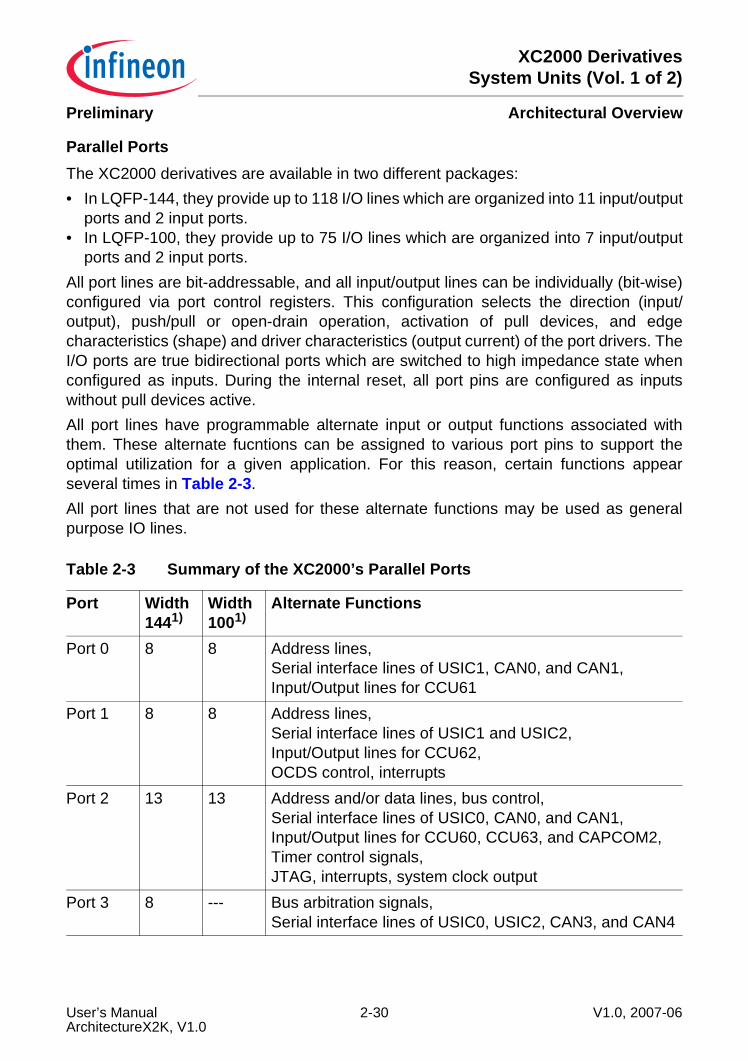
XC2000 DerivativesSystem Units (Vol. 1 of 2)
Architectural OverviewPreliminary
Parallel PortsThe XC2000 derivatives are available in two different packages:• In LQFP-144, they provide up to 118 I/O lines which are organized into 11 input/output
ports and 2 input ports.• In LQFP-100, they provide up to 75 I/O lines which are organized into 7 input/output
ports and 2 input ports.All port lines are bit-addressable, and all input/output lines can be individually (bit-wise)configured via port control registers. This configuration selects the direction (input/output), push/pull or open-drain operation, activation of pull devices, and edgecharacteristics (shape) and driver characteristics (output current) of the port drivers. TheI/O ports are true bidirectional ports which are switched to high impedance state whenconfigured as inputs. During the internal reset, all port pins are configured as inputswithout pull devices active.All port lines have programmable alternate input or output functions associated withthem. These alternate fucntions can be assigned to various port pins to support theoptimal utilization for a given application. For this reason, certain functions appearseveral times in Table 2-3.All port lines that are not used for these alternate functions may be used as generalpurpose IO lines.
Table 2-3 Summary of the XC2000’s Parallel Ports
Port Width1441)
Width1001)
Alternate Functions
Port 0 8 8 Address lines,Serial interface lines of USIC1, CAN0, and CAN1,Input/Output lines for CCU61
Port 1 8 8 Address lines,Serial interface lines of USIC1 and USIC2,Input/Output lines for CCU62,OCDS control, interrupts
Port 2 13 13 Address and/or data lines, bus control,Serial interface lines of USIC0, CAN0, and CAN1,Input/Output lines for CCU60, CCU63, and CAPCOM2,Timer control signals,JTAG, interrupts, system clock output
Port 3 8 --- Bus arbitration signals,Serial interface lines of USIC0, USIC2, CAN3, and CAN4
User’s Manual 2-30 V1.0, 2007-06ArchitectureX2K, V1.0
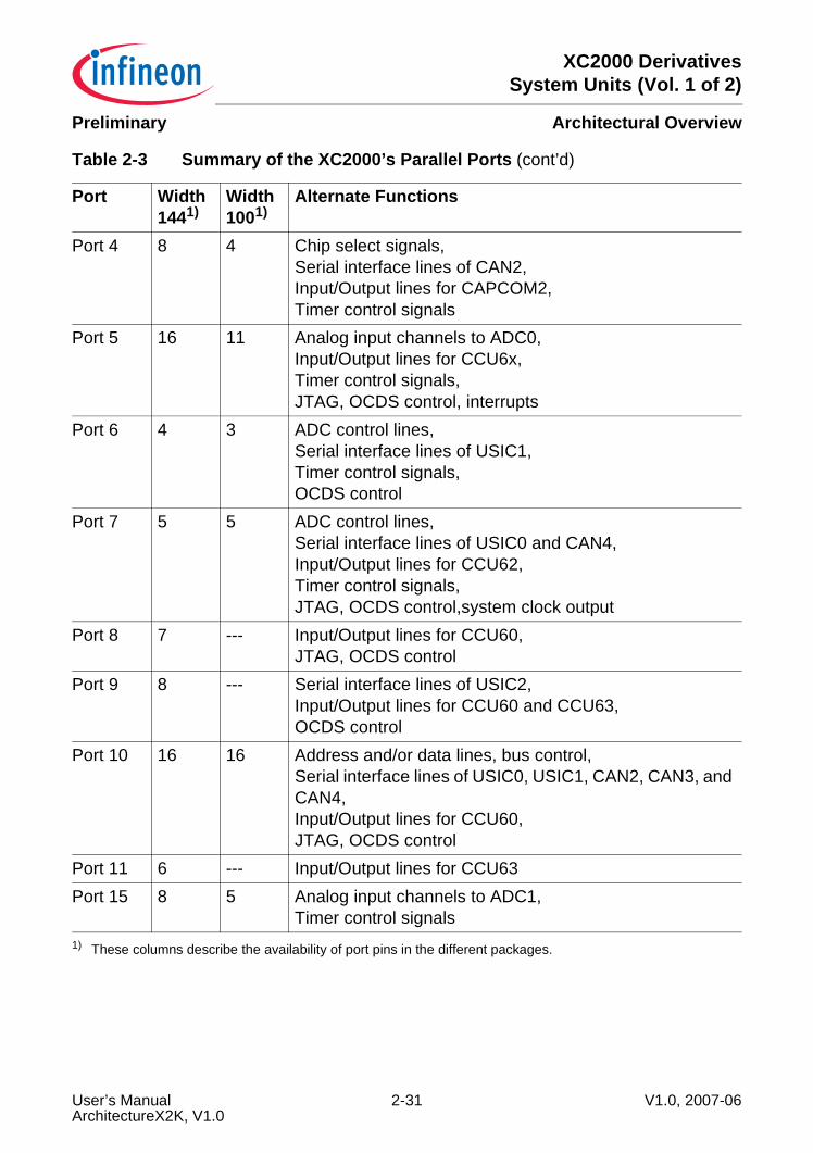
XC2000 DerivativesSystem Units (Vol. 1 of 2)
Architectural OverviewPreliminary
Port 4 8 4 Chip select signals,Serial interface lines of CAN2,Input/Output lines for CAPCOM2,Timer control signals
Port 5 16 11 Analog input channels to ADC0,Input/Output lines for CCU6x,Timer control signals,JTAG, OCDS control, interrupts
Port 6 4 3 ADC control lines,Serial interface lines of USIC1,Timer control signals,OCDS control
Port 7 5 5 ADC control lines,Serial interface lines of USIC0 and CAN4,Input/Output lines for CCU62,Timer control signals,JTAG, OCDS control,system clock output
Port 8 7 --- Input/Output lines for CCU60,JTAG, OCDS control
Port 9 8 --- Serial interface lines of USIC2,Input/Output lines for CCU60 and CCU63,OCDS control
Port 10 16 16 Address and/or data lines, bus control,Serial interface lines of USIC0, USIC1, CAN2, CAN3, and CAN4,Input/Output lines for CCU60,JTAG, OCDS control
Port 11 6 --- Input/Output lines for CCU63Port 15 8 5 Analog input channels to ADC1,
Timer control signals1) These columns describe the availability of port pins in the different packages.
Table 2-3 Summary of the XC2000’s Parallel Ports (cont’d)
Port Width1441)
Width1001)
Alternate Functions
User’s Manual 2-31 V1.0, 2007-06ArchitectureX2K, V1.0
XC2000 DerivativesSystem Units (Vol. 1 of 2)
Architectural OverviewPreliminary
2.4 Clock GenerationThe Clock Generation Unit uses a programmable on-chip PLL with multiple prescalersto generate the clock signals for the XC2000 with high flexibility. The master clock fMC isthe reference clock signal, and is used for TwinCAN and is output to the external system.The CPU clock fCPU and the system clock fSYS are derived from the master clock eitherdirectly (1:1) or via a 2:1 prescaler (fSYS = fCPU = fMC/2).The on-chip oscillator can drive an external crystal or accepts an external clock signal.The oscillator clock frequency can be multiplied by the on-chip PLL (by a programmablefactor) or can be divided by a programmable prescaler factor.If the bypass mode is used (direct drive or prescaler) the PLL can deliver an independentclock to monitor the clock signal generated by the on-chip oscillator. This PLL clock isindependent from the XTAL1 clock. When the expected oscillator clock transitions aremissing the Oscillator Watchdog (OWD) activates the PLL Unlock/OWD interrupt nodeand supplies the CPU with an emergency clock, the PLL clock signal. Under thesecircumstances the PLL will oscillate with its basic frequency.The oscillator watchdog can be disabled by switching the PLL off. This reduces powerconsumption, but also no interrupt request will be generated in case of a missingoscillator clock.
User’s Manual 2-32 V1.0, 2007-06ArchitectureX2K, V1.0

XC2000 DerivativesSystem Units (Vol. 1 of 2)
Architectural OverviewPreliminary
2.5 Power ManagementThe XC2000 provides several means to control the power it consumes either at a giventime or averaged over a certain timespan. Three mechanisms can be used (partly inparallel):• Supply Voltage Management allows the temporary reduction of the supply voltage
of major parts of the logic, or even the complete disconnection. This drasticallyreduces the power consumed because of leakage current, in particular at hightemperature.Several power reduction modes provide the optimal balance of power reduction andwake-up time.
• Clock Generation Management controls the distribution and the frequency ofinternal and external clock signals. While the clock signals for currently inactive partsof logic are disabled automatically, the user can reduce the XC2000’s CPU clockfrequency which drastically reduces the consumed power.External circuitry can be controlled via the programmable frequency output FOUT.
• Peripheral Management permits temporary disabling of peripheral modules. Eachperipheral can separately be disabled/enabled. Also the CPU can be switched offwhile the peripherals can continue to operate.
Wake-up from power reduction modes can be triggered either externally by signalsgenerated by the external system, or internally by the on-chip wake-up timer, whichsupports intermittent operation of the XC2000 by generating cyclic wake-up signals. Thisoffers full performance to quickly react on action requests while the intermittent sleepphases greatly reduce the average power consumption of the system.Note: When selecting the supply voltage and the clock source and generation method,
the required parameters must be carefully written to the respective bitfields, toavoid unintended intermediate states. Recommended sequences are providedwhich ensure the intended operation of power supply system and clock system.
User’s Manual 2-33 V1.0, 2007-06ArchitectureX2K, V1.0
XC2000 DerivativesSystem Units (Vol. 1 of 2)
Architectural OverviewPreliminary
2.6 On-Chip Debug Support (OCDS)The On-Chip Debug Support system provides a broad range of debug and emulationfeatures built into the XC2000. The user software running on the XC2000 can thus bedebugged within the target system environment.The OCDS is controlled by an external debugging device via the debug interface,consisting of the IEEE-1149-conforming JTAG port and a break interface. The debuggercontrols the OCDS via a set of dedicated registers accessible via the JTAG interface.Additionally, the OCDS system can be controlled by the CPU, e.g. by a monitor program.An injection interface allows the execution of OCDS-generated instructions by the CPU.Multiple breakpoints can be triggered by on-chip hardware, by software, or by anexternal trigger input. Single stepping is supported as well as the injection of arbitraryinstructions and read/write access to the complete internal address space. A breakpointtrigger can be answered with a CPU-halt, a monitor call, a data transfer, or/and theactivation of an external signal.The data transferred at a watchpoint (see above) can be obtained via the JTAG interfaceor via the external bus interface for increased performance.The debug interface uses a set of 6 interface signals (4 JTAG lines, 2 break lines) tocommunicate with external circuitry. These interface signals use dedicated pins.Complete system emulation is supported by an emulation device. Via this full-featuredemulation interface (including internal buses, control, status, and pad signals) thefunctions of the XC2000 chip can be emulated in an emulation system.
User’s Manual 2-34 V1.0, 2007-06ArchitectureX2K, V1.0
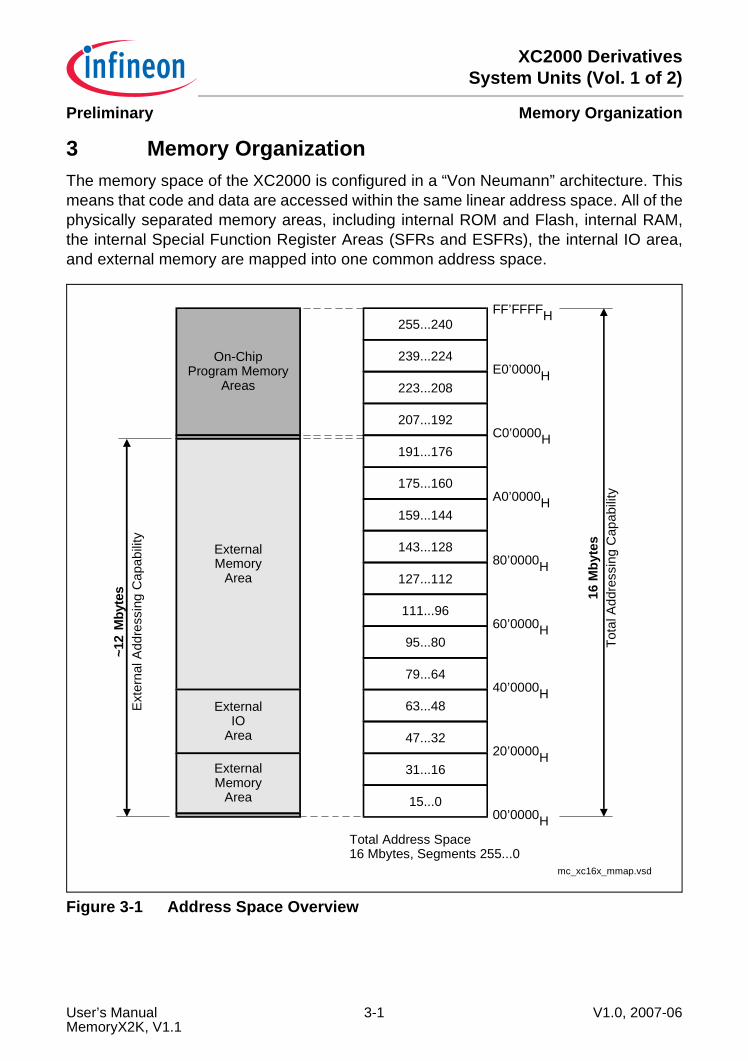
XC2000 DerivativesSystem Units (Vol. 1 of 2)
Memory OrganizationPreliminary
3 Memory OrganizationThe memory space of the XC2000 is configured in a “Von Neumann” architecture. Thismeans that code and data are accessed within the same linear address space. All of thephysically separated memory areas, including internal ROM and Flash, internal RAM,the internal Special Function Register Areas (SFRs and ESFRs), the internal IO area,and external memory are mapped into one common address space.
Figure 3-1 Address Space Overview
ExternalMemory
Area
On-ChipProgram Memory
Areas
mc_xc16x_mmap.vsd
239...224
223...208
191...176
175...160
159...144
143...128
127...112
111...96
95...80
79...64
63...48
47...32
31...16
15...000’0000H
C0’0000H
FF’FFFFH
40’0000H
80’0000H
16 M
byte
sTo
tal A
ddre
ssin
g C
apab
ility
Total Address Space16 Mbytes, Segments 255...0
255...240
207...192
20’0000H
60’0000H
A0’0000H
E0’0000H
ExternalIO
Area
ExternalMemory
Area
~12
Mby
tes
Ext
erna
l Add
ress
ing
Cap
abili
ty
User’s Manual 3-1 V1.0, 2007-06MemoryX2K, V1.1
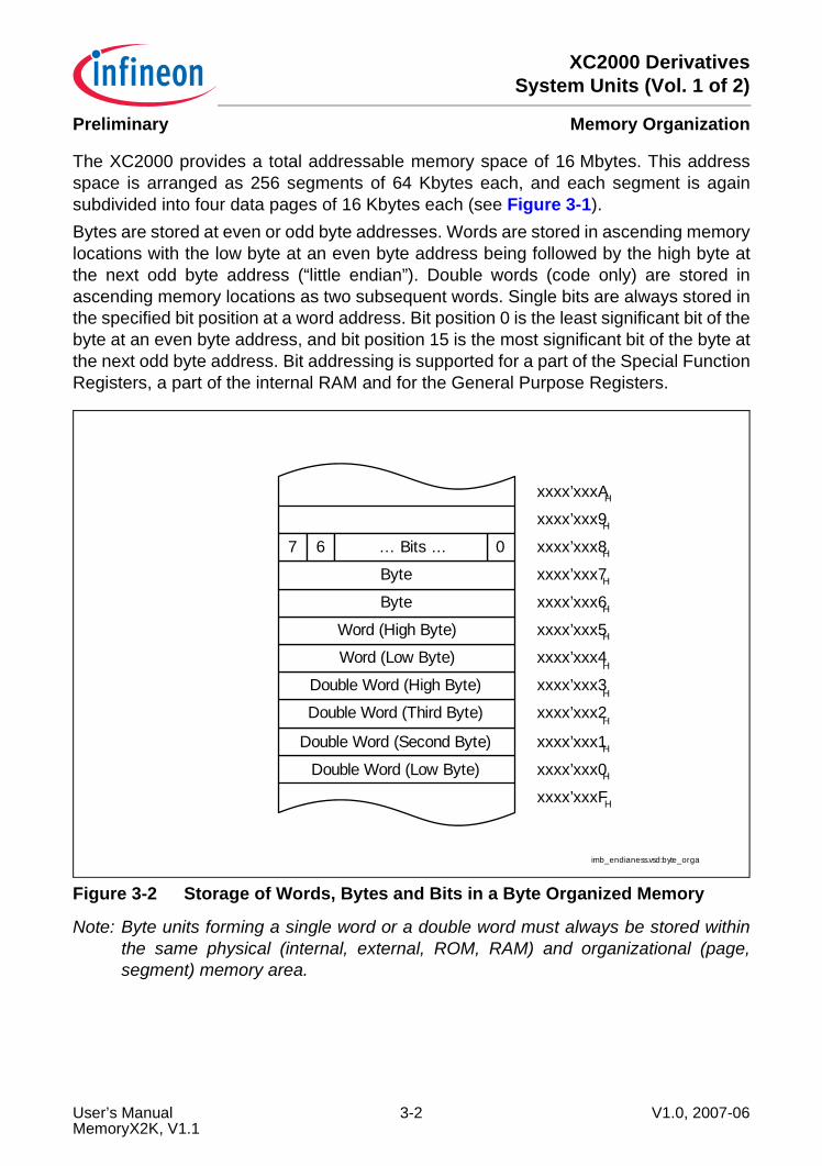
XC2000 DerivativesSystem Units (Vol. 1 of 2)
Memory OrganizationPreliminary
The XC2000 provides a total addressable memory space of 16 Mbytes. This addressspace is arranged as 256 segments of 64 Kbytes each, and each segment is againsubdivided into four data pages of 16 Kbytes each (see Figure 3-1).Bytes are stored at even or odd byte addresses. Words are stored in ascending memorylocations with the low byte at an even byte address being followed by the high byte atthe next odd byte address (“little endian”). Double words (code only) are stored inascending memory locations as two subsequent words. Single bits are always stored inthe specified bit position at a word address. Bit position 0 is the least significant bit of thebyte at an even byte address, and bit position 15 is the most significant bit of the byte atthe next odd byte address. Bit addressing is supported for a part of the Special FunctionRegisters, a part of the internal RAM and for the General Purpose Registers.
Figure 3-2 Storage of Words, Bytes and Bits in a Byte Organized Memory
Note: Byte units forming a single word or a double word must always be stored withinthe same physical (internal, external, ROM, RAM) and organizational (page,segment) memory area.
xxxx’xxxFH
xxxx’xxx0H
xxxx’xxx1H
xxxx’xxx2H
xxxx’xxx3H
xxxx’xxx4H
xxxx’xxx5H
xxxx’xxx6H
xxxx’xxx7H
xxxx’xxx8H
xxxx’xxx9H
xxxx’xxxAH
Double Word (Low Byte)
Double Word (Second Byte)
Double Word (Third Byte)
Double Word (High Byte)
Word (Low Byte)
Word (High Byte)
Byte
Byte
7 6 0… Bits ...
imb_endianess.vsd:byte_orga
User’s Manual 3-2 V1.0, 2007-06MemoryX2K, V1.1
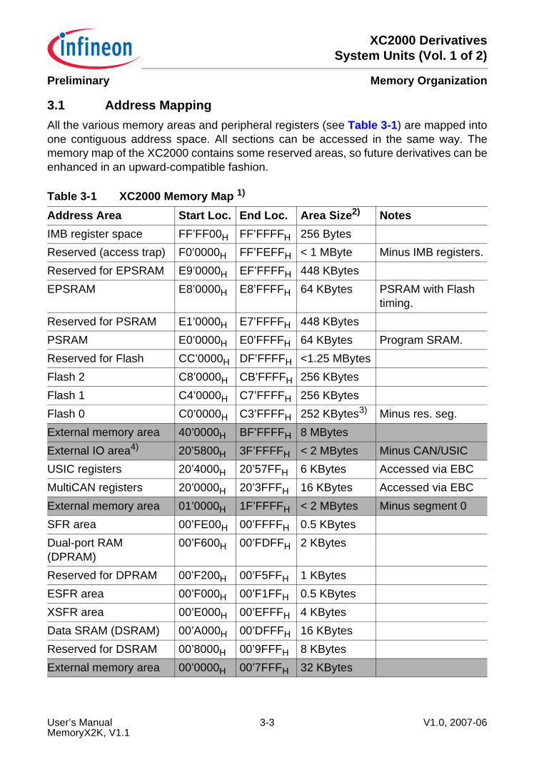
XC2000 DerivativesSystem Units (Vol. 1 of 2)
Memory OrganizationPreliminary
3.1 Address MappingAll the various memory areas and peripheral registers (see Table 3-1) are mapped intoone contiguous address space. All sections can be accessed in the same way. Thememory map of the XC2000 contains some reserved areas, so future derivatives can beenhanced in an upward-compatible fashion.
Table 3-1 XC2000 Memory Map 1)
Address Area Start Loc. End Loc. Area Size2) NotesIMB register space FF’FF00H FF’FFFFH 256 BytesReserved (access trap) F0’0000H FF’FEFFH < 1 MByte Minus IMB registers.Reserved for EPSRAM E9’0000H EF’FFFFH 448 KBytesEPSRAM E8’0000H E8’FFFFH 64 KBytes PSRAM with Flash
timing.Reserved for PSRAM E1’0000H E7’FFFFH 448 KBytesPSRAM E0’0000H E0’FFFFH 64 KBytes Program SRAM.Reserved for Flash CC’0000H DF’FFFFH <1.25 MBytesFlash 2 C8’0000H CB’FFFFH 256 KBytesFlash 1 C4’0000H C7’FFFFH 256 KBytesFlash 0 C0’0000H C3’FFFFH 252 KBytes3) Minus res. seg.External memory area 40’0000H BF’FFFFH 8 MBytesExternal IO area4) 20’5800H 3F’FFFFH < 2 MBytes Minus CAN/USICUSIC registers 20’4000H 20’57FFH 6 KBytes Accessed via EBCMultiCAN registers 20’0000H 20’3FFFH 16 KBytes Accessed via EBCExternal memory area 01’0000H 1F’FFFFH < 2 MBytes Minus segment 0SFR area 00’FE00H 00’FFFFH 0.5 KBytesDual-port RAM (DPRAM)
00’F600H 00’FDFFH 2 KBytes
Reserved for DPRAM 00’F200H 00’F5FFH 1 KBytesESFR area 00’F000H 00’F1FFH 0.5 KBytesXSFR area 00’E000H 00’EFFFH 4 KBytesData SRAM (DSRAM) 00’A000H 00’DFFFH 16 KBytesReserved for DSRAM 00’8000H 00’9FFFH 8 KBytesExternal memory area 00’0000H 00’7FFFH 32 KBytes
User’s Manual 3-3 V1.0, 2007-06MemoryX2K, V1.1
XC2000 DerivativesSystem Units (Vol. 1 of 2)
Memory OrganizationPreliminary
3.2 Special Function Register AreasThe Special Function Registers (SFRs) controlling the system and peripheral functionsof the XC2000 can be accessed via four dedicated address areas:• 512-byte SFR area (located above the internal RAM: 00’FFFFH … 00’FE00H).• 512-byte ESFR area (located below the internal RAM: 00’F1FFH … 00’F000H).• 4-Kbytes XSFR area (located below the ESFR area: 00’EFFFH … 00’E000H).• 256-byte IMB SFR area (located in: FF’FF00H … FF’FFFFH)1).This arrangement provides upward compatibility with the derivatives of the C166 andXC166 families.
1) Accesses to the shaded areas are reserved. In devices with external bus interface these accesses generateexternal bus accesses.
2) The areas marked with “<” are slightly smaller than indicated, see column “Notes”.3) The 4 KB sector from C0’F000H to C0’FFFFH is not accessible to the software.4) Several pipeline optimizations are not active within the external IO area. This is necessary to control external
peripherals properly.
1) Attention: the IMB SFR area is not recognized by the CPU as special IO area (see Section 3.6).
User’s Manual 3-4 V1.0, 2007-06MemoryX2K, V1.1
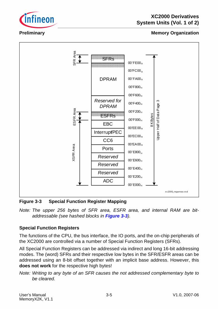
XC2000 DerivativesSystem Units (Vol. 1 of 2)
Memory OrganizationPreliminary
Figure 3-3 Special Function Register Mapping
Note: The upper 256 bytes of SFR area, ESFR area, and internal RAM are bit-addressable (see hashed blocks in Figure 3-3).
Special Function RegistersThe functions of the CPU, the bus interface, the IO ports, and the on-chip peripherals ofthe XC2000 are controlled via a number of Special Function Registers (SFRs).All Special Function Registers can be addressed via indirect and long 16-bit addressingmodes. The (word) SFRs and their respective low bytes in the SFR/ESFR areas can beaddressed using an 8-bit offset together with an implicit base address. However, thisdoes not work for the respective high bytes!Note: Writing to any byte of an SFR causes the not addressed complementary byte to
be cleared.
xc2000_regareas.vsd
00'E000H
ADC00'E200H
Reserved00'E400H
Reserved00'E600H
Reserved00'E800H
Ports00'EA00H
CC600'EC00H
Interrupt/PEC00'EE00H
EBC00'F000H
00'F200H
Reserved for DPRAM
00'F400H
00'F600H
00'F800H
00'FA00H
00'FC00H
00'FE00H
XSFR
Are
aES
FR A
rea
SFR
Are
a
Uppe
r Hal
f of D
ata
Pag
e 3
8 K
Byte
sESFRs
DPRAM
SFRs
User’s Manual 3-5 V1.0, 2007-06MemoryX2K, V1.1
XC2000 DerivativesSystem Units (Vol. 1 of 2)
Memory OrganizationPreliminary
The upper half of the SFR-area (00’FFFFH … 00’FF00H) and the ESFR-area (00’F1FFH… 00’F100H) is bit-addressable, so the respective control/status bits can be modifieddirectly or checked using bit addressing.When accessing registers in the ESFR area using 8-bit addresses or direct bitaddressing, an Extend Register (EXTR) instruction is required beforehand to switch theshort addressing mechanism from the standard SFR area to the Extended SFR area.This is not required for 16-bit and indirect addresses. The GPRs R15 … R0 areduplicated, i.e. they are accessible within both register blocks via short 2-, 4-, or 8-bitaddresses without switching.ESFR_SWITCH_EXAMPLE:EXTR #4 ;Switch to ESFR area for next 4 instr.MOV ODP9, #data16 ;ODP9 uses 8-bit reg addressingBFLDL DP9, #mask, #data8 ;Bit addressing for bitfieldsBSET DP1H.7 ;Bit addressing for single bitsMOV T8REL, R1 ;T8REL uses 16-bit mem address, ;R1 is duplicated into the ESFR space ;(EXTR is not required for this access);---- ;--------------- ;The scope of the EXTR #4 instruction … ;… ends here!MOV T8REL, R1 ;T8REL uses 16-bit mem address, ;R1 is accessed via the SFR space
In order to minimize the use of the EXTR instructions the ESFR area mostly holdsregisters which are mainly required for initialization and mode selection. Registers thatneed to be accessed frequently are allocated to the standard SFR area, whereverpossible.Note: The tools are equipped to monitor accesses to the ESFR area and will
automatically insert EXTR instructions, or issue a warning in case of missing orexcessive EXTR instructions.
Accesses to registers in the XSFR area use 16-bit addresses and require no specificaddressing modes or precautions.
General Purpose RegistersThe General Purpose Registers (GPRs) use a block of 16 consecutive words eitherwithin the global register bank or within one of the two local register banks. The bit-fieldBANK in register PSW selects the currently active register bank. The global register bankis mirrored to a section in the DPRAM, the Context Pointer (CP) register determines thebase address of the currently active global register bank section. This register bank mayconsist of up to 16 Word-GPRs (R0, R1, … R15) and/or of up to 16 byte-GPRs(RL0,RH0, … RL7, RH7). The sixteen byte-GPRs are mapped onto the first eight WordGPRs (see Table 3-2).
User’s Manual 3-6 V1.0, 2007-06MemoryX2K, V1.1
XC2000 DerivativesSystem Units (Vol. 1 of 2)
Memory OrganizationPreliminary
In contrast to the system stack, a register bank grows from lower towards higher addresslocations and occupies a maximum space of 32 bytes. The GPRs are accessed via short2-, 4-, or 8-bit addressing modes using the Context Pointer (CP) register as baseaddress for the global bank (independent of the current DPP register contents).Additionally, each bit in the currently active register bank can be accessed individually.
The XC2000 supports fast register bank (context) switching. Multiple global registerbanks can physically exist within the DPRAM at the same time. Only the global registerbank selected by the Context Pointer register (CP) is active at a given time, however.Selecting a new active global register bank is simply done by updating the CP register.A particular Switch Context (SCXT) instruction performs register bank switching byautomatically saving the previous context and loading the new context. The number ofimplemented register banks (arbitrary sizes) is limited only by the size of the availableDPRAM.Note: The local GPR banks are not memory mapped and the GPRs cannot be accessed
using a long or indirect memory address.
Table 3-2 Mapping of General Purpose Registers to DPRAM AddressesDPRAM Address High Byte Registers Low Byte Registers Word Registers<CP> + 1EH – – R15<CP> + 1CH – – R14<CP> + 1AH – – R13<CP> + 18H – – R12<CP> + 16H – – R11<CP> + 14H – – R10<CP> + 12H – – R9<CP> + 10H – – R8<CP> + 0EH RH7 RL7 R7<CP> + 0CH RH6 RL6 R6<CP> + 0AH RH5 RL5 R5<CP> + 08H RH4 RL4 R4<CP> + 06H RH3 RL3 R3<CP> + 04H RH2 RL2 R2<CP> + 02H RH1 RL1 R1<CP> + 00H RH0 RL0 R0
User’s Manual 3-7 V1.0, 2007-06MemoryX2K, V1.1

XC2000 DerivativesSystem Units (Vol. 1 of 2)
Memory OrganizationPreliminary
PEC Source and Destination PointersThe source and destination address pointers for data transfers on the PEC channels arelocated in the XSFR area.Each channel uses a pair of pointers stored in two subsequent word locations with thesource pointer (SRCPx) on the lower and the destination pointer (DSTPx) on the higherword address (x = 7 … 0). An additional segment register stores the associated sourceand destination segments, so PEC transfers can move data from/to any location withinthe complete addressing range.Whenever a PEC data transfer is performed, the pair of source and destination pointers(selected by the specified PEC channel number) accesses the locations referred to bythese pointers independently of the current DPP register contents.If a PEC channel is not used, the corresponding pointer locations can be used for otherpurposes.For more details about the use of the source and destination pointers for PEC datatransfers see Section XXX in Interrupt And Trap “Operation of PEC Channels”.Note: Writing to any byte of the PEC pointers causes the not addressed complementary
byte to be cleared.
User’s Manual 3-8 V1.0, 2007-06MemoryX2K, V1.1
XC2000 DerivativesSystem Units (Vol. 1 of 2)
Memory OrganizationPreliminary
3.3 Data Memory AreasThe XC2000 provides two on-chip RAM areas exclusively for data storage:• The Dual Port RAM (DPRAM) can be used for global register banks (GPRs), system
stack, storage of variables and other data, in particular for MAC operands.• The Data SRAM (DSRAM) can be used for system stack (recommended), storage
of variables and other data.Note: Data can also be stored in the PSRAM (see Section 3.10). However, both data
memory areas provide the fastest access.
Two additional on-chip memory areas exist with the special purpose to retain data whilethe system power domain is switched off:• The Stand-By RAM (SBRAM).• The Marker Memory (MKMEM).
Dual-Port RAM (DPRAM)The XC2000 provides 2 Kbytes of DPRAM (00’F600H … 00’FDFFH). Any word or bytedata in the DPRAM can be accessed via indirect or long 16-bit addressing modes, if theselected DPP register points to data page 3. Any word data access is made on an evenbyte address. The highest possible word data storage location in the DPRAM is00’FDFEH.For PEC data transfers, the DPRAM can be accessed independent of the contents of theDPP registers via the PEC source and destination pointers.The upper 256 bytes of the DPRAM (00’FD00H through 00’FDFFH) are provided forsingle bit storage, and thus they are bit addressable.Note: Code cannot be executed out of the DPRAM.
An area of 3 Kbytes is dedicated to DPRAM (00’F200H … 00’FDFFH). The locationswithout implemented DPRAM are reserved.
Data SRAM (DSRAM)The XC2000 provides 16 Kbytes of DSRAM (00’A000H … 00’CFFFH). Any word or bytedata in the DSRAM can be accessed via indirect or long 16-bit addressing modes, if theselected DPP register points to data page 3. Any word data access is made on an evenbyte address. The highest possible word data storage location in the DSRAM is00’CFFEH.For PEC data transfers, the DSRAM can be accessed independent of the contents of theDPP registers via the PEC source and destination pointers.Note: Code cannot be executed out of the DSRAM.
An area of 20 Kbytes is dedicated to DSRAM (00’8000H … 00’CFFFH). The locationwithout implemented DSRAM are reserved.
User’s Manual 3-9 V1.0, 2007-06MemoryX2K, V1.1
XC2000 DerivativesSystem Units (Vol. 1 of 2)
Memory OrganizationPreliminary
Stand-By RAM (SBRAM)The SBRAM provides 1 Kbyte of memory supplied by the wake-up power domain(DMP_M). Its main purpose is to retain state while the system power domain (DMP_1)is switched off.Unlike the other memories the SBRAM is not mapped into the address range of theprocessor. Reading and writing is done via two address and two data SFRs. Details ofthe access mechanism are described in Section 3.11.Note: Code cannot be executed out of the SBRAM.
Marker Memory (MKMEM)The MKMEM provides 4 bytes of memory supplied by the wake-up power domain. Itspurpose is the same as the SBRAM.The MKEM consists of 2 16-bit SFRs that are accessible as all other SFRs. Details aredescribed in Section 3.11.Note: It goes without saying that code cannot be executed out of the MKMEM.
User’s Manual 3-10 V1.0, 2007-06MemoryX2K, V1.1
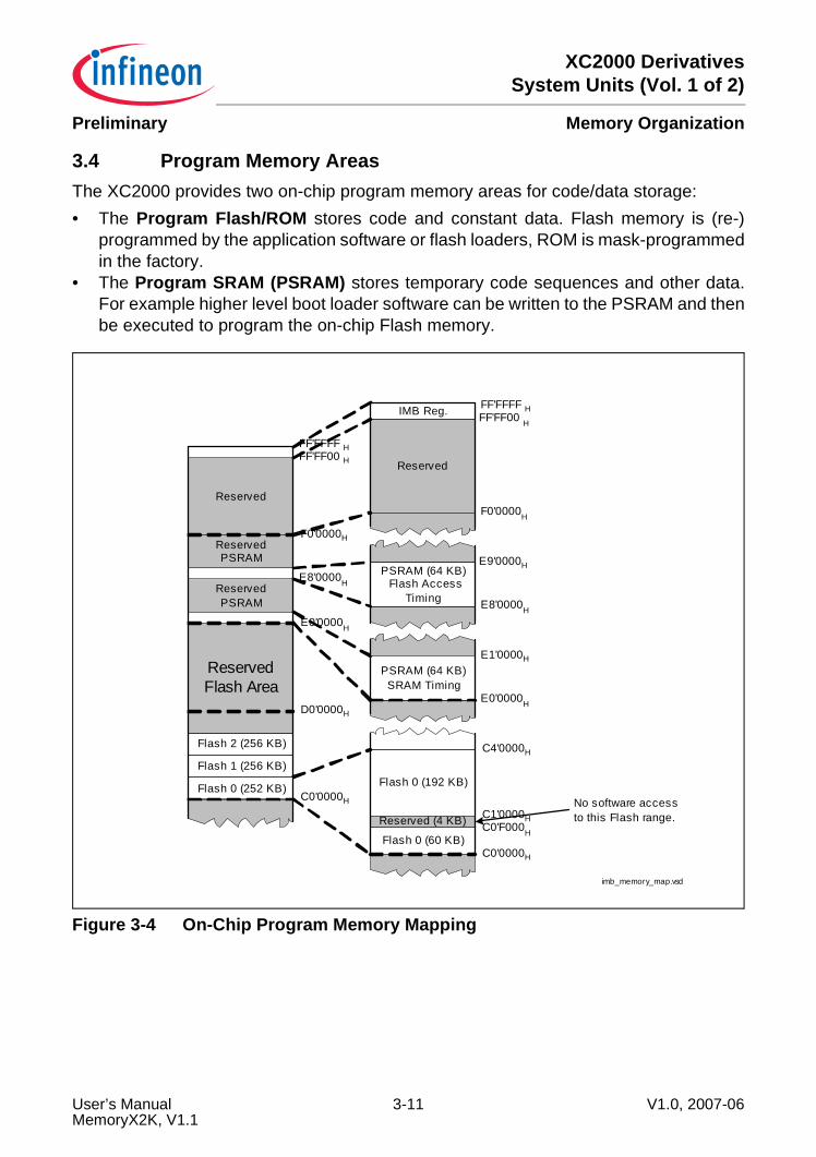
XC2000 DerivativesSystem Units (Vol. 1 of 2)
Memory OrganizationPreliminary
3.4 Program Memory AreasThe XC2000 provides two on-chip program memory areas for code/data storage:• The Program Flash/ROM stores code and constant data. Flash memory is (re-)
programmed by the application software or flash loaders, ROM is mask-programmedin the factory.
• The Program SRAM (PSRAM) stores temporary code sequences and other data.For example higher level boot loader software can be written to the PSRAM and thenbe executed to program the on-chip Flash memory.
Figure 3-4 On-Chip Program Memory Mapping
Reserved
ReservedPSRAM
ReservedPSRAM
ReservedFlash Area
Reserved
Flash 0 (252 KB)
Flash 1 (256 KB)
Flash 2 (256 KB)
C0'0000H
D0'0000H
E0'0000H
F0'0000H
FF'FF00 H
PSRAM (64 KB)SRAM Timing
E0'0000H
E1'0000H
E8'0000H
imb_memory_map.vsd
PSRAM (64 KB)Flash Access
Timing E8'0000H
E9'0000H
IMB Reg. FF'FF00 H
FF'FFFF H
F0'0000H
Flash 0 (60 KB)
Flash 0 (192 KB)
Reserved (4 KB)
C0'0000H
C0'F000H
C1'0000H
C4'0000H
No software accessto this Flash range.
FF'FFFF H
User’s Manual 3-11 V1.0, 2007-06MemoryX2K, V1.1
XC2000 DerivativesSystem Units (Vol. 1 of 2)
Memory OrganizationPreliminary
3.4.1 Program/Data SRAM (PSRAM)The XC2000 provides 64 Kbytes of PSRAM (E0’0000H … E0’FFFFH). The PSRAMprovides fast code execution without initial delays. Therefore, it supports non-sequentialcode execution, for example via the interrupt vector table.Any word or byte data in the PSRAM can be accessed via indirect or long 16-bitaddressing modes, if the selected DPP register points to one of its data page 896 – 899.Any word data access is made on an even byte address. The highest possible word datastorage location in the PSRAM is E0’FFFEH.For PEC data transfers, the PSRAM can be accessed independent of the contents of theDPP registers via the PEC source and destination pointers.Any data can be stored in the PSRAM. Because the PSRAM is optimized for codefetches, however, data accesses to the data memories provide higher performance.Note: The PSRAM is not bit-addressable.
An area of 512 Kbytes is dedicated to PSRAM (E0’0000H … F7’FFFFH). The locationswithout implemented PSRAM are reserved.
Flash EmulationDuring code development the PSRAM will often be used for storing code or data that theproduction chip will later contain in the flash memory. In order to ensure similar executiontime the PSRAM supports a second access path in the range E8’0000H … EF’FFFFHwith timing parameters that correspond to Flash timing. The number of wait-cycles isdetermined by the flash access timing configuration (see IMB_IMBCTRL.WSFLASH).Writes are always performed without wait-cycles.This flash access timing imitation is nearly cycle accurate because the same read logicas for reading the flash memory is used1). Discrepancies might occur if the software usesthe PSRAM for flash emulation and directly as PSRAM. During emulation accessconflicts can cause a slightly different timing as in the product chip where these conflictsdo not occur.Another source of timing differences can be access conflicts at the flash modules in theproduct chip. Data reads and instruction fetches that target different flash modules canbe executed concurrently whereas if they target the same flash module they areexecuted sequentially with the data access as first. In the flash emulation this type ofconflict can not occur. The data and the instruction access will both incur the definednumber of wait-cycles (as if they would target different flash modules) and if they collideat the PSRAM interface the instruction fetch will see an additional wait-cycle.
1) The dual use of the flash read logic might cause unexpected behavior: while the IMB Core is busy withupdating the protection configuration (after startup or after changing the security pages) read accesses to theflash emulation range of the PSRAM are blocked because Flash data reads would be blocked also.
User’s Manual 3-12 V1.0, 2007-06MemoryX2K, V1.1
XC2000 DerivativesSystem Units (Vol. 1 of 2)
Memory OrganizationPreliminary
Data IntegrityThe PSRAM contains its own parity generation and comparison logic. It generates theparity bits for every written byte. When reading data it checks the data integrity bycomparing the read parity bits with calculated parity bits.If enabled parity errors can trigger a trap (see “Memory Parity Error Handling” onPage 3-77).
Write ProtectionAs the PSRAM is often used to store timing critical code or constant data it is suppliedwith a write protection. After storing critical data in the PSRAM the register fieldIMB_IMBCTRH.PSPROT can be used to split the PSRAM into a read-only and awritable part. Write accesses to the read-only part are blocked and a trap can beactivated.
3.4.2 Non-Volatile Program Memory (Flash)The XC2000 provides 764 Kbytes of program Flash (C0’0000H … CB’FFFFH). Code anddata fetches are always 64-bit aligned, using byte select lines for word and byte data.Any word or byte data in the program memory can be accessed via indirect or long 16-bit addressing modes, if the selected DPP register points to one of the respective datapages. Any word data access is made on an even byte address. The highest possibleword data storage location in the program memory is CB’FFFEH.For PEC data transfers, the program memory can be accessed independent of thecontents of the DPP registers via the PEC source and destination pointers.Note: The program memory is not bit-addressable.
An area of 2 Mbytes is dedicated to program memory (C0’0000H … DF’FFFFH). Thelocations without implemented program memory are reserved.A more detailed description can be found in “Embedded Flash Memory” onPage 3-18.
User’s Manual 3-13 V1.0, 2007-06MemoryX2K, V1.1
XC2000 DerivativesSystem Units (Vol. 1 of 2)
Memory OrganizationPreliminary
3.5 System StackThe system stack may be defined anywhere within the XC2000’s memory areas(including external memory).For all system stack operations the respective stack memory is accessed via a 24-bitstack pointer. The Stack Pointer (SP) register provides the lower 16 bits of the stackpointer (stack pointer offset), the Stack Pointer Segment (SPSEG) register adds theupper 8 bits of the stack pointer (stack segment). The system stack grows downwardfrom higher towards lower locations as it is filled. Only word accesses are supported tothe system stack.Register SP is decremented before data is pushed on the system stack, andincremented after data has been pulled from the system stack. Only word accesses aresupported to the system stack.By using register SP for stack operations, the size of the system stack is limited to64 KBytes. The stack must be located in the segment defined by register SPSEG.The stack pointer points to the latest system stack entry, rather than to the next availablesystem stack address.A stack overflow (STKOV) register and a stack underflow (STKUN) register are providedto control the lower and upper limits of the selected stack area. These two stackboundary registers can be used both for protection against data corruption.For best performance it is recommended to locate the stack to the DPRAM or to theDSRAM. Using the DPRAM may conflict with register banks or MAC operands.
User’s Manual 3-14 V1.0, 2007-06MemoryX2K, V1.1
XC2000 DerivativesSystem Units (Vol. 1 of 2)
Memory OrganizationPreliminary
3.6 IO AreasThe following areas of the XC2000’s address space are marked as IO area:• The external IO area is provided for external peripherals (or memories) and also
comprises the on-chip LXBus-peripherals, such as the CAN or USIC modules. It islocated from 20’0000H to 3F’FFFFH (2 Mbytes).
• The internal IO area provides access to the internal peripherals and is split into threeblocks:– The SFR area, located from 00’FE00H to 00’FFFFH (512 bytes).– The ESFR area, located from 00’F000H to 00’F1FFH (512 bytes).– The XSFR area, located from 00’E000H to 00’EFFFH (4 Kbytes).
Note: The external IO area supports real byte accesses. The internal IO area does notsupport real byte transfers, the complementary byte is cleared when writing to abyte location.
The IO areas have special properties, because peripheral modules must be controlledin a different way than memories:• Accesses are not buffered and cached, the write back buffers and caches are not
used to store IO read and write accesses.• Speculative reads are not executed, but delayed until all speculations are solved (e.g.
pre-fetching after conditional branches).• Data forwarding is disabled, an IO read access is delayed until all IO writes pending
in the pipeline are executed, because peripherals can change their internal state aftera write access.
User’s Manual 3-15 V1.0, 2007-06MemoryX2K, V1.1
XC2000 DerivativesSystem Units (Vol. 1 of 2)
Memory OrganizationPreliminary
3.7 External Memory SpaceThe XC2000 is capable of using an address space of up to 16 Mbytes. Only parts of thisaddress space are occupied by internal memory areas or are reserved. A total area ofapproximately 12 Mbytes references external memory locations. This external memoryis accessed via the XC2000’s external bus interface.Selectable memory bank sizes are supported: The maximum size of a bank in theexternal memory space depends on the number of activated address bits. It can varyfrom 64 Kbytes (with A15 … A0 activated) to 12 Mbytes (with A23 … A0 activated). Thelogical size of a memory bank and its location in the address space is defined byprogramming the respective address window. It can vary from 4 Kbytes to 12 Mbytes.• Non-segmented mode:
– 64 Kbytes with A15 … A0 on PORT0 or PORT1.• 1-bit segmented mode:
– 128 Kbytes with A16 on Port 4– and A15 … A0 on PORT0 or PORT1.
• 2-bit … 7-bit segmented mode:– with Ax … A16 on Port 4– and A15 … A0 on PORT0 or PORT1.
• 8-bit segmented mode:– 12 Mbytes with A23 … A16 on Port 4– and A15 … A0 on PORT0 or PORT1.
Each bank can be directly addressed via the address bus, while the programmable chipselect signals can be used to select various memory banks.The XC2000 also supports four different bus types:• Multiplexed 16-bit Bus with address and data on PORT0 (default after Reset).• Multiplexed 8-bit Bus with address and data on PORT0/P0L.• Demultiplexed 16-bit Bus with address on PORT1 and data on PORT0.• Demultiplexed 8-bit Bus with address on PORT1 and data on P0L.Memory model and bus mode are preselected during reset by pin EA and PORT0 pins.For further details about the external bus configuration and control please refer toChapter XX (The External Bus Controller).External word and byte data can only be accessed via indirect or long 16-bit addressingmodes using one of the four DPP registers. There is no short addressing mode forexternal operands. Any word data access is made to an even byte address.For PEC data transfers the external memory can be accessed independent of thecontents of the DPP registers via the PEC source and destination pointers.Note: The external memory is not bit addressable.
User’s Manual 3-16 V1.0, 2007-06MemoryX2K, V1.1

XC2000 DerivativesSystem Units (Vol. 1 of 2)
Memory OrganizationPreliminary
3.8 Crossing Memory BoundariesThe address space of the XC2000 is implicitly divided into equally sized blocks ofdifferent granularity and into logical memory areas. Crossing the boundaries betweenthese blocks (code or data) or areas requires special attention to ensure that thecontroller executes the desired operations.Memory Areas are partitions of the address space assigned to different kinds ofmemory (if provided at all). These memory areas are the SFR areas, the on-chipprogram or data RAM areas, the on-chip ROM/Flash (if available), the on-chip LXBus-peripherals (if integrated), and the external memory.Accessing subsequent data locations which belong to different memory areas is noproblem. However, when executing code, the different memory areas must be switchedexplicitly via branch instructions. Sequential boundary crossing is not supported andleads to erroneous results.Note: Changing from the external memory area to the on-chip RAM area takes place
within segment 0.
Segments are contiguous blocks of 64 Kbytes each. They are referenced via the CodeSegment Pointer CSP for code fetches and via an explicit segment number for dataaccesses overriding the standard DPP scheme.During code fetching, segments are not changed automatically, but rather must beswitched explicitly. The instructions JMPS, CALLS and RETS will do this.In larger sequential programs, make sure that the highest used code location of asegment contains an unconditional branch instruction to the respective followingsegment to prevent the pre-fetcher from trying to leave the current segment.Data Pages are contiguous blocks of 16 Kbytes each. They are referenced via the datapage pointers DPP3 … DPP0 and via an explicit data page number for data accessesoverriding the standard DPP scheme. Each DPP register can select one of the possible1024 data pages. The DPP register which is used for the current access is selected viathe two upper bits of the 16-bit data address. Therefore, subsequent 16-bit dataaddresses which cross the 16-Kbytes data page boundaries will use different data pagepointers, while the physical locations need not be subsequent within memory.
User’s Manual 3-17 V1.0, 2007-06MemoryX2K, V1.1
XC2000 DerivativesSystem Units (Vol. 1 of 2)
Memory OrganizationPreliminary
3.9 Embedded Flash MemoryThis chapter describes the embedded flash memory of the XC2000:• Section 3.9.1 defines the flash specific nomenclature and the structure of the flash
memory.• Section 3.9.2 describes the operating modes.• Section 3.9.3 contains all operations.• Section 3.9.4 gives the details of operating sequences.• The three sections Section 3.9.5, Section 3.9.6 and Section 3.9.7 look more into
depth of maintaining data integrity and protection issues.• Section 3.9.8 discusses Flash EEPROM emulation.• Section 3.9.9 describes interrupt generation by the flash memory.The Chapter 3.10 describes how the flash memory is embedded into the memoryarchitecture of the XC2000 and lists all SFRs that affect its behavior.
3.9.1 DefinitionsThis section defines the nomenclature and some abbreviations as a base for the rest ofthe document. The used flash memory is a non-volatile memory (“NVM”) based on afloating gate one-transistor cell. It is called “non-volatile” because the memory content iskept when the memory power supply is shut off.
Logical and Physical StatesFlash memory content can not be changed directly as in SRAMs. Changing data is acomplicated process with a typically much longer duration than reading.• Erasing: The erased state of a cell is logical 0. Forcing an flash cell to this state is
called “erasing”. Erasing is possible with a minimum granularity of one page (seebelow).
• Programming: The programmed state of a cell is logical 1. Changing an erased cellto this state is called “programming”. A page must only be programmed once and hasto be erased before it can be programmed again.
The above listed processes have certain limitations:• Retention: This is the time during which the data of a flash cell can be read reliably.
The retention time is a statistical figure that depends on the operating conditions ofthe flash array (temperature profile) and the accesses to the flash array. With anincreasing number of program/erase cycles (see endurance) the retention is lowered.Drain and gate disturbs decrease data retention as well.
• Endurance: As described above the data retention is reduced with an increasingnumber of program/erase cycles. A flash cell incurs one cycle whenever its page orsector is erased. This number is called “endurance”. As said for the retention it is astatistical figure that depends on operating conditions and the use of the flash cellsand not to forget on the required quality level.
User’s Manual 3-18 V1.0, 2007-06MemoryX2K, V1.1
XC2000 DerivativesSystem Units (Vol. 1 of 2)
Memory OrganizationPreliminary
• Drain Disturb: Because of using a so called “one-transistor” flash cell each programaccess disturbs all pages of the same sector slightly. Over long these “drain disturbs”make 0 and 1 values indistinguishable and thus provoke read errors. This effect isagain interrelated with the retention. A cell that incurred a high number of draindisturbs will have a lower retention. The physical sectors of the flash array areisolated from each other. So pages of a different sector do not incur a drain disturb.This effect must be therefor considered when the page erase feature is used.
The durations of programming and erasing as well as the limits for endurance, retentionand drain disturbs are documented in the data sheet.Attention: No means exist in the device that prevent the application from violating
these limitation.
Array StructureThe flash memory is hierarchically structured:• Block: A block consists of 128 user data bits (i.e. 16 bytes) and 9 ECC bits. One read
access delivers one block.• Page: A page consists of 8 blocks (i.e. 128 bytes). Programming changes always
complete pages.• Sector: A sector consists of 32 pages (i.e. 4096 bytes). The pages of one sector are
affected by drain disturb as described above. The pages of different sectors areisolated from each other.
• Array: Each array has in the XC2000 64 sectors1). Usually when referring to an“array” this contains as well all accompanying logic as assembly buffer, high voltagelogic and the digital logic that allows to operate them in parallel.
• Memory: The complete flash memory of the XC2000 consists of 3 flash arrays.This structure is visualized in Figure 3-5.
1) In the Flash0 one sector is reserved for device internal purposes. It is not accessible by software.
User’s Manual 3-19 V1.0, 2007-06MemoryX2K, V1.1
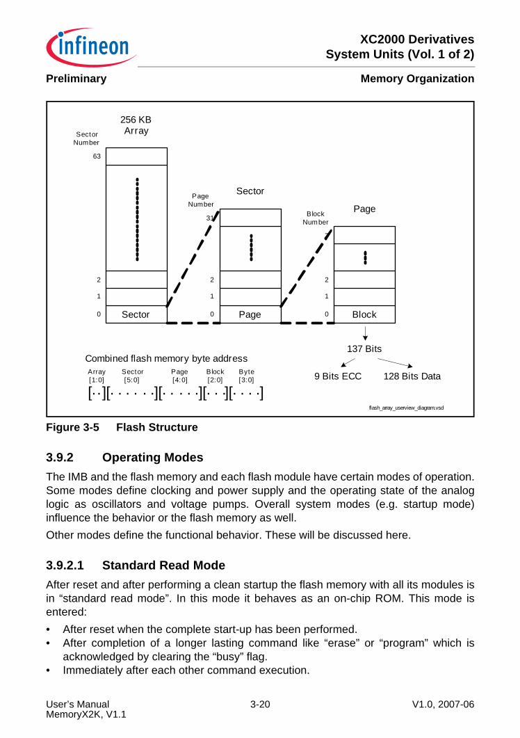
XC2000 DerivativesSystem Units (Vol. 1 of 2)
Memory OrganizationPreliminary
Figure 3-5 Flash Structure
3.9.2 Operating ModesThe IMB and the flash memory and each flash module have certain modes of operation.Some modes define clocking and power supply and the operating state of the analoglogic as oscillators and voltage pumps. Overall system modes (e.g. startup mode)influence the behavior or the flash memory as well.Other modes define the functional behavior. These will be discussed here.
3.9.2.1 Standard Read ModeAfter reset and after performing a clean startup the flash memory with all its modules isin “standard read mode”. In this mode it behaves as an on-chip ROM. This mode isentered:• After reset when the complete start-up has been performed.• After completion of a longer lasting command like “erase” or “program” which is
acknowledged by clearing the “busy” flag.• Immediately after each other command execution.
flash_array_userview_diagram.vsd
256 KBArraySector
Number
0
1
2
63
SectorPageNumber
0
1
2
31PageBlock
Number
0
1
2
7
Sector Page Block
137 Bits
9 Bits ECC 128 Bits Data
Combined flash memory byte addressArray[1:0]
[ ][ ][ ][ ][ ].. . . . . . . . . . . . . . . . . . .Sector[5:0]
Page[4:0]
Block[2:0]
Byte[3:0]
User’s Manual 3-20 V1.0, 2007-06MemoryX2K, V1.1
XC2000 DerivativesSystem Units (Vol. 1 of 2)
Memory OrganizationPreliminary
• In case of detecting an execution error like attempting to write to a write protectedrange, sending a wrong password, after all sequence errors.
For the long lasting commands the read mode stays active until the last command of thesequence is received and the operation is started.
3.9.2.2 Command ModeAfter receiving the last command of a command sequence the addressed flash module(not the whole flash memory!) is placed into command mode. For most commands thiswill not be noticed by the user as the command executes immediately and afterwards theflash module is placed again into read mode. For the long lasting commands the flashmodule stays in command mode for several milliseconds. This is reported by setting thecorresponding “busy” flag. The data of a busy flash module cannot be read. Newcommand sequences are not accepted (even if they target different flash modules) andcause a sequence error until the running operation has finished.Read accesses to busy flash modules stall the CPU until the read mode is entered again.A stalled CPU responds only to the reset. As no interrupts can be handled this state mustbe avoided. Nevertheless this feature can be used to execute code from a flash modulethat erases or programs data in the same flash module.The IMB Core is limited to control only one running operation. Consequently when oneflash module is in command mode no other commands to either modules are acceptedbut the other modules stay readable.
3.9.2.3 Page ModeThe page mode is entered with the “Enter Page Mode” command. Please find itsdescription below. A flash module that is in page mode can still be read (so it isconcurrently in “read mode”). At a time only one flash module can be in page mode.When the flash memory is in page mode — i.e. one of the flash modules is in page mode— some command sequences are not allowed. These are all erase sequences and the“change read margin” sequence. These are ignored and a sequence error is reported.
User’s Manual 3-21 V1.0, 2007-06MemoryX2K, V1.1
XC2000 DerivativesSystem Units (Vol. 1 of 2)
Memory OrganizationPreliminary
3.9.3 OperationsThe flash memory supports the following operations:• Instruction fetch.• Data read.• Command sequences to change data and control the protection.
3.9.3.1 Instruction Fetch from Flash MemoryInstructions are fetched by the PMU in groups of aligned 64 bits. These code requestsare forwarded to the flash memory. It needs a varying number of cycles (depending onthe system clock frequency) to perform the read access. The number of cycles must beknown to the IMB Core because the flash does not signal data availability. The numberof wait-cycles is therefore stored in the IMB_IMBCTRL register.One read access to the flash memory delivers 128 data bits and a 9-bit ECC value. TheECC value is used to detect and possibly correct errors. The addressed 64-bit part of the128-bit chunk is sent to the PMU. The complete 128 data bits and the 9 ECC bits arestored in the IMB Core with their address. If a succeeding fetch request matches thisaddress the data is delivered from the buffer without performing a read access in theflash memory. The delivery from the buffer happens after one cycle. The flash read wait-cycles are not waited.The stored data are a kind of instruction cache. In order to support self-modifying code(e.g. boot loaders) this cache is invalidated when the corresponding address is written(i.e. erased or programmed).In addition to this fetch buffer the IMB Core has an additional performance increasingfeature — the Linear Code Pre-Fetch. When this feature is enabled withIMB_IMBCTRL.DLCPF = 0 the IMB Core fetches autonomously the followinginstructions while the CPU executes from its own buffers or the fetch buffer. As thisfeature is fetching only the linear successors (it does not analyze the code stream) it ismost effective for code with longer linear sequences. For code with a high density ofjumps and calls it can even cause a reduction of performance and should be switchedoff.
User’s Manual 3-22 V1.0, 2007-06MemoryX2K, V1.1
XC2000 DerivativesSystem Units (Vol. 1 of 2)
Memory OrganizationPreliminary
3.9.3.2 Data Reads from Flash MemoryData reads are issued by the DMU. Data is always requested in 16-bit words. The flashmemory delivers for every read request 128 bits plus ECC as described in “InstructionFetch from Flash Memory” on Page 3-22.The IMB Core has to get all 128 bits to evaluate the ECC data. The requested 16 bits willbe delivered to the DMU. All data and ECC bits are kept in the data register and theiraddress is kept in the address register. For all following data reads the address iscompared with the address register and in case of a match the data is delivered after onecycle from the data register. Every data read that is not delivered from this cacheinvalidates the cache content. When the requested data arrives the cache contains againvalid data.This small data cache is invalidated when a write (i.e. erase or program) access to thisaddress happens.For data reads the IMB Core does not perform any autonomous pre-fetching.
3.9.3.3 Data Writes to Flash MemoryFlash memory content can not be changed by directly writing data to this memory.Command sequences are used to execute all other operations in the flash exceptreading. Command sequences consist of data writes with certain data to the flashmemory address range. All data moves targeting this range are interpreted as commandsequences. If they do not match a defined one or if the IMB Core is busy with executinga sequence (i.e. it is in “command mode”) a sequence error is reported.
User’s Manual 3-23 V1.0, 2007-06MemoryX2K, V1.1
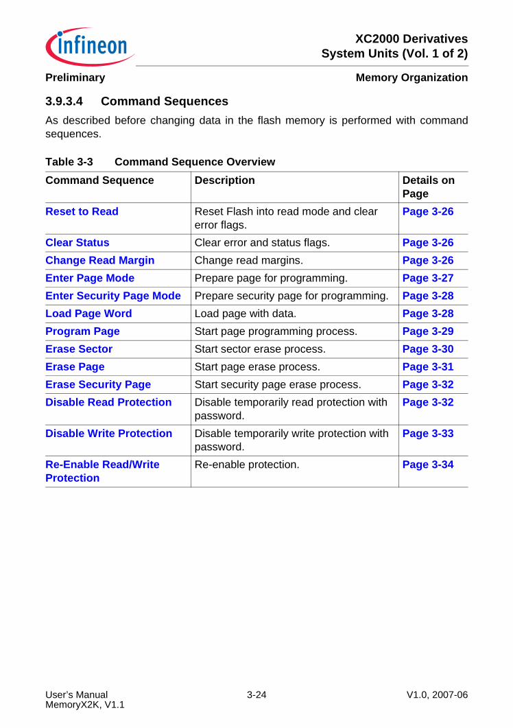
XC2000 DerivativesSystem Units (Vol. 1 of 2)
Memory OrganizationPreliminary
3.9.3.4 Command SequencesAs described before changing data in the flash memory is performed with commandsequences.
Table 3-3 Command Sequence OverviewCommand Sequence Description Details on
PageReset to Read Reset Flash into read mode and clear
error flags.Page 3-26
Clear Status Clear error and status flags. Page 3-26Change Read Margin Change read margins. Page 3-26Enter Page Mode Prepare page for programming. Page 3-27Enter Security Page Mode Prepare security page for programming. Page 3-28Load Page Word Load page with data. Page 3-28Program Page Start page programming process. Page 3-29Erase Sector Start sector erase process. Page 3-30Erase Page Start page erase process. Page 3-31Erase Security Page Start security page erase process. Page 3-32Disable Read Protection Disable temporarily read protection with
password.Page 3-32
Disable Write Protection Disable temporarily write protection with password.
Page 3-33
Re-Enable Read/Write Protection
Re-enable protection. Page 3-34
User’s Manual 3-24 V1.0, 2007-06MemoryX2K, V1.1
XC2000 DerivativesSystem Units (Vol. 1 of 2)
Memory OrganizationPreliminary
3.9.4 Details of Command SequencesThe description defines the command sequence with pseudo assembler code. It is“pseudo” because all addresses are direct addresses which is generally not possible inreal assembler code.The commands are called by a sequence of one to six data moves into the flash memoryrange. The data moves must be of the “word” type, i.e. not byte move instructions. Thefollowing sections describe each command. The following abbreviations for addressesand data will be used:• PA: “Page Address”. This is the base address of the destination page. For example
the very first page has the address C0’0000H. The page 13 of the second array hasthe PA = C0’0000H + 1·256·1024 (for the array) + 0·4·1024 (for the sector) + 13·128(for the page) = C4’0680H.
• SECPA: “Security Page Address”. This is the virtual address of a security page. It is“virtual” because SECPA is just used as argument of the command sequence toidentify the security page but the physical storage of the security page is hidden.Two security pages are defined:SecP0: address C0’0000H.SecP1: address C0’0080H.
• WD: “Write Data”. This is a 16-bit data word that is written into the assembly buffer.• SA: “Sector Address”. This is the physical sector number as defined in Figure 3-6
based on the address of the flash module. Two examples as clarification:1. Physical sector number 16 of the first array that is based on C0’0000H is addressedwith SA = C0’0000H + 16·4·1024 = C1’0000H.2. The second 256 KB array has the base address C4’0000H (as shown inTable 3-1). So its physical sector number 3 has the SA = C4’0000H + 3·4·1024 =C4’3000H.
• PWD: “Password”. This is a 64-bit password. It is transferred in 4 16-bit data wordsPWD0 = PWD[15:0], PWD1 = PWD[31:16], PWD2 = PWD[47:32] and PWD3 =PWD[63:48].
• Address XX followed by two hexadecimal digits, for example “XXAAH”. If thecommand targets a certain flash module the XX must be translated to its baseaddress. So “XXAAH” means C0’00AAH for all commands addressing flash 0,C4’00AAH for flash 1 and C8’00AAH for flash 2. If a command (e.g. “Clear Status”)addresses the complete flash memory the base address of flash module 0 must beused.
• Data XX followed by two hexadecimal digits, e.g. XXA5H. This is a “don’t care” dataword where only the low byte must match a certain pattern. So in this example all datawords like 12A5H or 79A5H can be used.
• MR: “Margin”. This 8-bit number defines the read margin. MR can take the values 00H(normal read), 01H (hard read 0), 02H (alternate hard read 0), 05H (hard read 1), 06H(alternate hard read 1). All other values of MR are reserved.
User’s Manual 3-25 V1.0, 2007-06MemoryX2K, V1.1
XC2000 DerivativesSystem Units (Vol. 1 of 2)
Memory OrganizationPreliminary
Reset to ReadArguments: –Definition: MOV XXAAH, XXF0HTiming: One cycle command that does not set any “BUSY” flags. But note that animmediately following write access to the IMB Core is stalled for a few clock cycles duringwhich the IMB Core is busy with aborting a previous command.Description: The internal command state machine is reset to initial state and returns toread mode. An already started programming or erase operation is not affected and willbe continued (the “Reset to Read” command — i.e. all commands — will anyhow not beaccepted while the IMB Core is busy).The “Reset to Read” command is a single cycle command. It can be used during acommand sequence to reset the command interpreter and return the IMB Core into itsinitial state. It clears also all error flags in the Flash Status Register IMB_FSR and anactive page mode is aborted. Because all commands are rejected with a SQER while theIMB Core is busy “Reset to Read” can not be used to abort an active command mode.This command clears: PROER, PAGE, SQER, OPER, ISBER, IDBER, DSBER,DDBER.
Clear StatusArguments: –Definition: MOV XXAAH, XXF5HTiming: 1-cycle command that does not set any busy flags.Description: The flags OPER, SQER, PROER, ISBER, IDBER, DSBER, DDBER inFlash status register are cleared. Additionally, the process status bits (PROG, ERASE,POWER, MAR) are cleared.
Change Read MarginArguments: MRDefinition: MOV XXAAH, XXB0H MOV XX54H, XXMRHTiming: 2-cycle command that sets “BUSY” for around 30 micro seconds.Description: This command sequence changes the read margin of one flash module.The address XX of the second move identifies the targeted flash module. The flashmodule needs some time to change its read voltage. During this time BUSY is set andthis flash module cannot be accessed. The other flash modules stay readable.
User’s Manual 3-26 V1.0, 2007-06MemoryX2K, V1.1

XC2000 DerivativesSystem Units (Vol. 1 of 2)
Memory OrganizationPreliminary
The argument “MR” defines the read margin:• 00H: normal read margin.• 01H: hard read 0 margin.• 02H: alternate hard read 0 margin.• 05H: hard read 1 margin.• 06H: alternate hard read 1 margin.• Other values: reserved.For understanding the read margins please refer to “Read Margins” on Page 3-35.This command must not be issued when the flash memory is in page mode. In this caseit is ignored and a sequence error is reported.Note: As noted in “Margin Control” on Page 3-60 the command sequences “Program
Page”, “Erase Sector”, “Erase Page” and “Erase Security Page” reset the readmargin back to 00H, i.e. to the normal read margin. The same happens in case ofa flash wake-up.
Enter Page ModeArguments: PADefinition: MOV XXAAH, XX50H MOV PA, XXAAHTiming: 2-cycle command that sets “BUSY” for around 100 clock cycles.Description: The page mode is entered to prepare a page programming operation onpage address PA. (Write data are accepted only with the “Load Page Word” command.)With this command, the IMB Core initializes the write pointer of its block assemblyregister to zero so that it points to the first word. The page mode is indicated in the statusregister IMB_FSR with the PAGE bit, separately for each flash module. The page modeand the read mode are allowed in parallel at the same time and in the same flash moduleso the flash module stays readable. When the addressed page PA is read the content ofthe flash memory is delivered. The page mode can be aborted and the related PAGE bitin IMB_FSR be cleared with the “Reset to Read” command. A new “Enter Page Mode”command during page mode aborts the actual page mode, which is indicated with theerror flag SQER, and restarts a new page operation. So as mentioned above only oneof the flash modules can be in page mode at a time. If one of the erase commands or the“Change Read Margin” command are received while in page mode it is ignored and asequence error is reported.If write protection is installed for the sector to be programmed, the “Enter Page Mode”command is only accepted when write protection has before been disabled using theunlock command sequence “Disable Write Protection” with four passwords. If globalwrite protection is installed with read protection, also the command “Disable ReadProtection” can be used if no sector specific protection is installed. If write protection is
User’s Manual 3-27 V1.0, 2007-06MemoryX2K, V1.1
XC2000 DerivativesSystem Units (Vol. 1 of 2)
Memory OrganizationPreliminary
not disabled when the “Enter Page Mode” command is received, the command is notexecuted, and the protection error flag PROER is set in the IMB_FSR.
Enter Security Page ModeArguments: SECPADefinition: MOV XXAAH, XX55H MOV SECPA, XXAAHTiming: 2-cycle command that sets “BUSY” for around 100 clock cycles.Description: This command is identical to the “Enter Page Mode” command (seeabove), with the following exceptions: The addressed page (SECPA) belongs to thesecurity pages of the flash memory and not to the user flash range. This command canonly be executed after disabling of read protection and of sector write protection. Only ifprotection is not installed (e.g. for the very first installation of keywords), read/writeprotection need not be disabled. This command is not accepted and a protection error isreported if any protection is installed and active.The use of this command to install passwords and to disable them again is described in“Protection Handling Details” on Page 3-38.
Load Page WordArguments: WDDefinition: MOV XXF2H, WD
Timing: 1-cycle command that does not set any “BUSY” flags. But note that animmediately following write access to the IMB Core or read from the flash memory isstalled for a few clock cycles if it arrives while the IMB Core is busy with copying its blockassembly register content into the flash module assembly buffer. During this stall timethe CPU can not perform any action! So either the user software can accept this stall time(which must be taken into account for the worst-case interrupt latency) or the softwaremust avoid the blocking accesses.Description: Load the IMB Core block assembly register with a 16-bit word andincrement the write pointer. The 128 byte assembly buffer (i.e. a complete page) is filledby a sequence of 64 “Load Page Word” commands. The word address is not determinedby the command but the “Enter Page Mode” command sets a write word pointer to zerowhich is incremented after each “Load Page Word” command.This (sequential) data write access to the block assembly register belongs to and is onlyaccepted in Page Mode. The command address of this single cycle command is alwaysthe same (F2H). These low order address bits also identify the “Load Page Word”command and the sequential write data to be loaded into the block assembly register.
User’s Manual 3-28 V1.0, 2007-06MemoryX2K, V1.1
XC2000 DerivativesSystem Units (Vol. 1 of 2)
Memory OrganizationPreliminary
The high order bits XX should address the target page. The IMB Core takes always thepage address that was used by the last “Enter Page Mode” command.When the 128-bit block assembly register of the IMB Core is filled completely after 8“Load Page Word” commands the IMB Core calculates the 9 ECC bits and transfers theblock into the assembly buffer of the flash module. After that it sets the write pointer ofthe block assembly register back to zero. The following 8 “Load Page Word” commandsfill again the block. After all 8 blocks are filled the “Program Page” command can beused to trigger the program process that transfers the assembly buffer content into theflash array.While the IMB Core transfers the completed block assembly register to the flash moduleit can not accept new data for a few cycles. A “Load Page Word” command arrivingduring this time is stalled by the IMB Core.If “Program Page” is called before all blocks of the assembly buffer have received newdata then the remaining bits are cleared.If more than 8 times 8 commands are used the additional data is lost. The overflowcondition is indicated by the sequence error flag, but the execution of a following“Program Page” command is not suppressed (the page mode is not aborted).When a “Load Page Word” command is received and the flash is not in page mode, asequence error is reported in IMB_FSR with SQER flag. In case of a new “Enter PageMode” command or a “Reset to Read” command during page mode, or in case of anApplication Reset, the write data in the assembly buffer is lost. The current page modeis aborted and in case of a new “Enter Page Mode” command entered again for the newaddress.
Program PageArguments: –Definition: MOV XXAAH, XXA0H MOV XX5AH, XXAAHTiming: 2-cycle command that sets “BUSY” for the whole programming duration.Description: The assembly buffer of the flash module is programmed into the flash array.If the last block of data was not filled completely this command finalizes its ECCcalculation and copies its data into the assembly buffer before it starts the programprocess. The selection of the flash module and the page to be programmed depends onthe page address used by the last “Enter Page Mode” command. The user softwareshould always address the targeted page.The programming process is autonomously performed by the selected flash module. TheCPU is not occupied and can continue with its application.
User’s Manual 3-29 V1.0, 2007-06MemoryX2K, V1.1
XC2000 DerivativesSystem Units (Vol. 1 of 2)
Memory OrganizationPreliminary
The “Program Page” command is only accepted if the addressed flash module is inPage Mode (otherwise, a sequence error is reported instead of execution). With the“Program Page” command, the page mode is terminated, indicated by resetting therelated PAGE flag and the command mode is entered and the PROG flag in the statusregister IMB_FSR is activated and the BUSY flag for the addressed module is set inIMB_FSR. While BUSY is set the IMB Core does not accept any further commands.When the program process has finished BUSY is cleared but PROG stays set. Itindicates which operation has finished and will be cleared by a System Reset or by“Clear Status”.Read accesses to the busy flash module are not possible. Reading a busy flash modulestalls until the flash module becomes ready again.If write protection is installed for the sector to be programmed, the “Program Page”command is not accepted because the Flash is not in Page Mode (see description of the“Enter Page Mode” command).If the page to be programmed is a security page (accepted only in security page mode),the new protection configuration (including keywords or protection confirmation code) isvalid directly after execution of this command.While the IMB Core reads the new protection configuration all DMU accesses to anyflash module are stalled.
Erase SectorArguments: SADefinition: MOV XXAAH, XX80H MOV XX54H, XXAAH MOV SA, XX33HTiming: 3-cycle command that sets BUSY for the whole erasing duration.Description: The addressed physical sector in the flash array is erased. Following datareads deliver all-zero data with correct ECC.The erasing process is autonomously performed by the selected flash module. The CPUis not occupied and can continue with its application.The sector to be erased is addressed by SA (sector address) in the last command cycle.With the last cycle of the “Erase Sector” command, the command mode is entered,indicated by activation of the ERASE flag and after start of erase operation also by therelated busy flag in the status register IMB_FSR. The BUSY flag is cleared after finishingthe operation but ERASE stays set. It can be cleared by a System Reset or the “ClearStatus” command.
User’s Manual 3-30 V1.0, 2007-06MemoryX2K, V1.1
XC2000 DerivativesSystem Units (Vol. 1 of 2)
Memory OrganizationPreliminary
Read accesses to the busy flash module are not possible. Read accesses to the not busyflash module are especially supported. Reading a busy flash module stalls until the flashmodule becomes ready again.If write protection is installed for the sector to be erased, the Erase Sector command isonly accepted when write protection has before been disabled using the unlockcommand sequence “Disable Write Protection”. If global write protection is installedwith read protection, also the command “Disable Read Protection” can be used if nosector specific protection is installed. If write protection is not disabled when the “EraseSector” command is received, the command is not executed, and the protection errorflag PROER is set in the IMB_FSR.This command must not be issued when the flash memory is in page mode. In this caseit is ignored and a sequence error is reported.
Erase PageArguments: PADefinition: MOV XXAAH, XX80H MOV XX54H, XXAAH MOV PA, XX03HTiming: 3-cycle command that sets BUSY for the whole erasing duration.Description: The addressed page is erased. Following data reads deliver all-zero datawith correct ECC.With the last cycle of the “Erase Page” command, the command mode is entered,indicated by activation of the ERASE flag and after start of erase operation also by therelated BUSY flag in the status register IMB_FSR. BUSY is cleared automatically afterfinishing the operation but ERASE stays set. It is cleared by a System Reset or the“Clear Status” command.Read accesses to the busy flash array are not possible. Read accesses to the not busyflash modules are especially supported. Reading a busy flash module stalls until theflash module becomes ready again.If the page to be erased belongs to a sector which is write protected, the command isonly executed when write protection has before been disabled (see “Erase Sector”command).In case of using the page erase care must be taken not to exceed the drain disturb limitof the other pages of the same sector.This command must not be issued when the flash memory is in page mode. In this caseit is ignored and a sequence error is reported.
User’s Manual 3-31 V1.0, 2007-06MemoryX2K, V1.1
XC2000 DerivativesSystem Units (Vol. 1 of 2)
Memory OrganizationPreliminary
Erase Security PageArguments: SECPADefinition: MOV XXAAH, XX80H MOV XX54H, XXA5H MOV SECPA, XX53HTiming: 3-cycle command that sets BUSY for the whole erasing duration.Description: The addressed security page is erased.This command is identical to the “Erase Page” command with the following exceptions:The addressed page (SecP0 or SecP1) belongs not to the user visible flash memoryrange. This command can only be executed after disabling of read protection and ofsector write protection.See “Protection Handling Examples” on Page 3-45 for a detailed description of re-programming security pages.The structure of the two security pages (SecP0 and SecP1) is described in “Layout ofthe Security Pages” on Page 3-43.After erasing a security page the new protection configuration (including keywords orprotection confirmation code) is valid directly after execution of this command.While the IMB Core reads the protection configuration all DMU accesses to any flashmodule are stalled.This command must not be issued when the flash memory is in page mode. In this caseit is ignored and a sequence error is reported.
Disable Read ProtectionArguments: PWDDefinition: MOV XX3CH, XXXXH MOV XX54H, PWD0 MOV XXAAH, PWD1 MOV XX54H, PWD2 MOV XXAAH, PWD3 MOV XX5AH, XX55HTiming: 6-cycle command that does not set any busy flag.Description: Disable temporarily Flash read protection and — if activated — global writeprotection of the whole flash memory. The RPA bit in IMB_IMBCTR is reset.This is a protected command sequence, using four user defined passwords to releasethis command or to check the programmed keywords. For every password onecommand cycle is required. If the second or fourth password represents the code of the
User’s Manual 3-32 V1.0, 2007-06MemoryX2K, V1.1
XC2000 DerivativesSystem Units (Vol. 1 of 2)
Memory OrganizationPreliminary
“Reset to Read” command, it is interpreted as password and the reset is not executed.The 16-bit passwords are internally compared with the keywords out of the “SecurityPage 0”. If one or more passwords are not identical to their related keywords, theprotected sectors remain in the locked state and a protection error (PROER) is indicatedin the Flash status register. In this case, a new “Disable Read Protection” command ora “Disable Write Protection” command is only accepted after the next ApplicationReset.Note: During execution of the “Disable Read” (or Write) Protection command a
password compare error is only indicated after all four passwords have beencompared with the related keywords.
Note: This command sequence is also used to check the correctness of keywordsbefore the protection is confirmed in the Security Page 1. A wrong keyword isindicated by the IMB_FSR flag PROER.
After correct execution of this command, the whole flash memory is unlocked and theread protection disable bit RPRODIS is set in the Flash Status Register (IMB_FSR).Erase and program operations on all sectors are then possible, if the flash memory wasalso globally write protected (WPA=1), and if they are not separately write protected. Theread protection (including global write protection, if so selected) remains disabled untilthe command “Re-Enable Read/Write Protection” is executed, or until the nextApplication Reset (including HW and SW reset).
Disable Write ProtectionArguments: PWDDefinition: MOV XX3CH, XXXXH MOV XX54H, PWD0 MOV XXAAH, PWD1 MOV XX54H, PWD2 MOV XXAAH, PWD3 MOV XX5AH, XX05HTiming: 6-cycle command that does not set any busy flag.Description: Disable temporarily the global flash write protection or/and the sector writeprotection of all protected sectors. The WPA bit in IMB_IMBCTR is reset.This is a protected command sequence, using four user defined passwords to releasethis command (as described above for the “Disable Read Protection” command).After correct execution of this command, all write-protected sectors are unlocked, whichis indicated in the Flash Status Register (IMB_FSR) with the WPRODIS bit. Erase andprogram operations on all sectors are now possible, until• The command “Re-Enable Read/Write Protection” is executed, or
User’s Manual 3-33 V1.0, 2007-06MemoryX2K, V1.1
XC2000 DerivativesSystem Units (Vol. 1 of 2)
Memory OrganizationPreliminary
• The next Application Reset (including HW and SW reset) is received.
Re-Enable Read/Write ProtectionArguments: –Definition: MOV XX5EH, XXXXHTiming: 1-cycle command that does not set any busy flags.Description: Flash read and write protection is resumed.This single-cycle command clears RPRODIS and WPRODIS. The IMB Core is triggeredto restore the protection states RPA and WPA from the content of the security page 0 asdefined in Table 3-4 ““Flash State” Determining RPA and WPA” on Page 3-40. Soin effect this command resumes all kinds of temporarily disabled protection installations.This command is released immediately after execution.
User’s Manual 3-34 V1.0, 2007-06MemoryX2K, V1.1
XC2000 DerivativesSystem Units (Vol. 1 of 2)
Memory OrganizationPreliminary
3.9.5 Data IntegrityThis section describes means for detecting and preventing the inadvertent modificationof data in the flash memory.
3.9.5.1 Error Correcting Codes (ECC)With very low probability a flash cell can lose its data value faster than specified. In orderto reach the defined overall device reliability each 128-bit block of flash data isaccompanied with a 9-bit ECC value. This redundancy supplies SEC-DED capability,meaning “single error correction and double error detection”. All single bit errors arecorrected (and the incident is detected), all double bit errors are detected and even mosttriple bit errors are detected but some of these escape as valid data or corrected data.A detected error is reported in the register IMB_FSR_PROT. Software can select whichtype of error should trigger a trap by the means of register IMB_INTCTR. In the systemcontrol further means exist to modify the handling of errors (see “SCU Trap ControlRegisters” on Page 6-202). The enabled trap requests by the flash module are handledthere as “Flash Access Trap”. In case of a double-bit error the read data is alwaysreplaced with a dummy data word.
3.9.5.2 Aborted Program/Erase DetectionWhere the ECC should protect from intrinsic failures of the flash memory that affectusually only single bits; an interruption of a running program or erase process mightcause massive data corruption:• The erase process programs first all cells to 1 before it erases them. So depending
on the time when it is interrupted the data might be in a different state. This can bethe old data, all-one, a random value, a weak all-zero or finally all-zero.
• The program process programs all bits concurrently from 0 to 1. If it is interrupted notall set bits might read as 1 or contain a weak 1.
The register IMB_FSR_OP contains the bits ERASE and PROG. These bits stay set untilthe next “Clear Status” command or System Reset. So if an erase or program processis interrupted by an Application Reset one of these bits is still set which allows to detectthe interruption. It lies in the responsibility of the software to send the “Clear Status”command after a finalized program/erase process to enable this evaluation.Another possible measure against aborted program/erase processes is to prevent resetsby configuring the SCU appropriately.
3.9.5.3 Read MarginsAs explained above interrupting a program or erase process might leave cells in aweakly erased or programmed state. This is particularly dangerous as following readsmight deliver the correct data with correct ECC but these cells do not have the defined
User’s Manual 3-35 V1.0, 2007-06MemoryX2K, V1.1
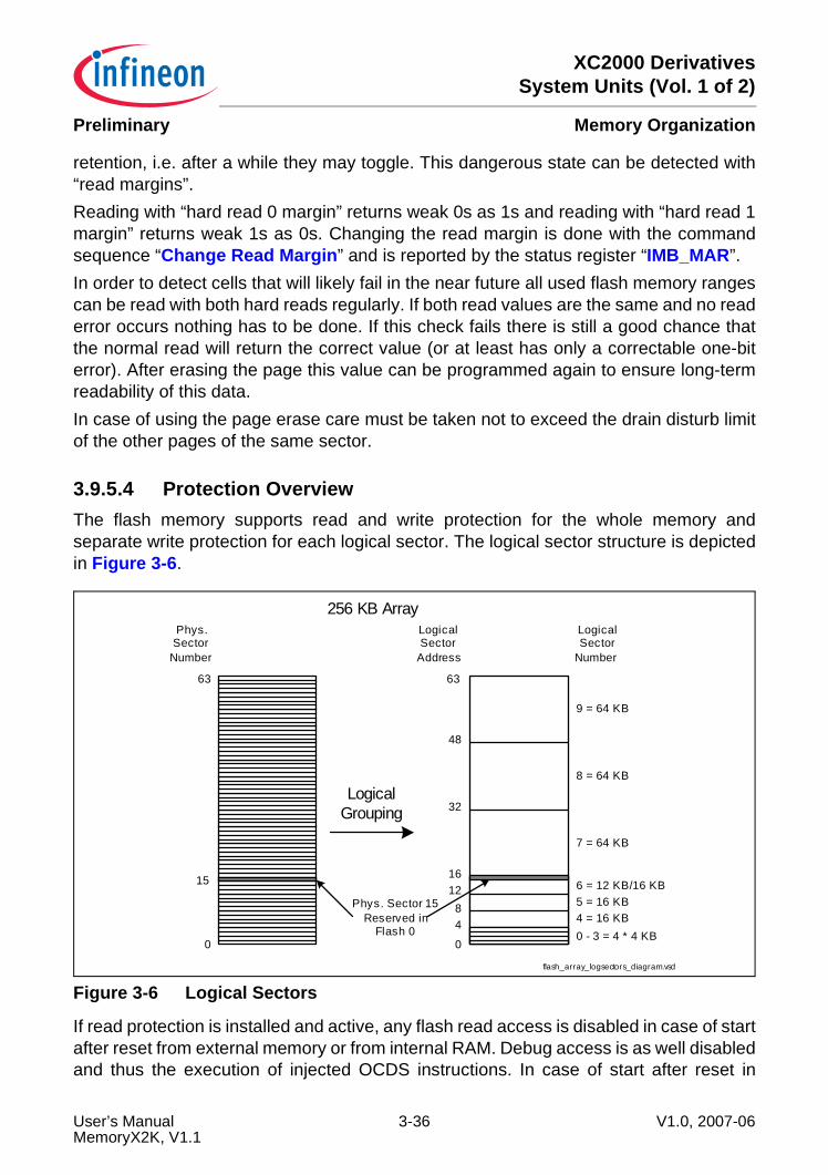
XC2000 DerivativesSystem Units (Vol. 1 of 2)
Memory OrganizationPreliminary
retention, i.e. after a while they may toggle. This dangerous state can be detected with“read margins”.Reading with “hard read 0 margin” returns weak 0s as 1s and reading with “hard read 1margin” returns weak 1s as 0s. Changing the read margin is done with the commandsequence “Change Read Margin” and is reported by the status register “IMB_MAR”.In order to detect cells that will likely fail in the near future all used flash memory rangescan be read with both hard reads regularly. If both read values are the same and no readerror occurs nothing has to be done. If this check fails there is still a good chance thatthe normal read will return the correct value (or at least has only a correctable one-biterror). After erasing the page this value can be programmed again to ensure long-termreadability of this data.In case of using the page erase care must be taken not to exceed the drain disturb limitof the other pages of the same sector.
3.9.5.4 Protection OverviewThe flash memory supports read and write protection for the whole memory andseparate write protection for each logical sector. The logical sector structure is depictedin Figure 3-6.
Figure 3-6 Logical Sectors
If read protection is installed and active, any flash read access is disabled in case of startafter reset from external memory or from internal RAM. Debug access is as well disabledand thus the execution of injected OCDS instructions. In case of start after reset in
flash_array_logsectors_diagram.vsd
256 KB ArrayPhys.
SectorNumber
0
63
LogicalGrouping
LogicalSector
Address
0
63
48
1216
32
48
LogicalSector
Number
0 - 3 = 4 * 4 KB4 = 16 KB5 = 16 KB6 = 12 KB/16 KB
7 = 64 KB
8 = 64 KB
9 = 64 KB
Phys. Sector 15Reserved in
Flash 0
15
User’s Manual 3-36 V1.0, 2007-06MemoryX2K, V1.1
XC2000 DerivativesSystem Units (Vol. 1 of 2)
Memory OrganizationPreliminary
internal flash, all flash access operations are controlled by the flash-internal user codeand are therefore allowed, as long as not especially disabled by the user, e.g. beforeenabling the debug interface.Per default, the read protection includes a full (global) flash memory write protectioncovering all flash modules. This is necessary to eliminate the possibility to program adump routine into the Flash, which reads the whole Flash and writes it out via theexternal bus or a serial interface. Program and erase accesses to the flash during activeread protection are only possible, if write protection is separately disabled. Flash writeand read protection can be temporarily disabled, if the user authorizes himself withcorrect passwords.The device also features a sector specific write protection. Software locking of flashmemory sectors is provided to protect code and data. This feature disables both programand erase operations for all protected sectors. With write protection it is supported toprotect the flash memory or parts of it from unauthorized programming or eraseaccesses and to provide virus-proof protection for all sectors.Read and write protection is installed by specific security configuration words which areprogrammed by the user directly into two “Security Pages” (SecP0/1). After any reset,the security configuration is checked by the command state machine (IMB Core) andinstallations are stored (and indicated) in related registers. If any protection is enabledalso the security pages are especially protected.For authorization of short-term disabling of read protection or/and of write protection apassword checking feature is provided. Only with correct 64-bit password a temporaryunprotected state is taken and the protected command sequences are enabled. If notfinished by the command “Re-Enable Read/Write Protection”, the unprotected state isterminated with the next reset. Password checking is based on four 16-bit keywords(together 64 bits) which are programmed by the user directly into the “Security Page 0”(SecP0).Special support is provided to protect also the protection installation itself against anystressing or beaming aggressors. The codes of configuration bits are selected, so thatin case of any violation in the flash array, on the read path or in registers the protectedstate is taken per default. In registers and security pages, protection control bits arecoded always with two bits, having both codes, “00B” and “11B” as indication of illegaland therefore protected state.
User’s Manual 3-37 V1.0, 2007-06MemoryX2K, V1.1

XC2000 DerivativesSystem Units (Vol. 1 of 2)
Memory OrganizationPreliminary
3.9.6 Protection Handling DetailsAs shortly described in “Protection Overview” on Page 3-36 the flash memory can bein different protection states. The protection handling can be separated into differentlayers that interact which each other (see Figure 3-7).• The lowest layer consists of the physical content of the security pages SecP0 and
SecP1. This information is used to initialize the protection system during startup.• The next layer consists of registers that report the state of the physical layer
(IMB_PROCONx) and the protection state (IMB_FSR). The protection state can betemporarily changed with command sequences which is reflected in the IMB_FSR.
• The highest layer is represented by 4 fields of the IMB_IMBCTR register. These fieldsdefine the protection rights of the customer software (are read or write accessescurrently allowed or not).
The IMB Core controls the protection state of all connected flash modules centrally. Inthis position it can supervise all accesses that are issued by the CPU.
Figure 3-7 Protection Layers
Physical Layer
Middle Layer
IMB_FSR
RPRO
WPRODIS
PROINERPROIN
RPRODIS
IMB_PROCONx PROCONs
Lock Code
RPROPasswords PROCONs
IMB_FSR
Security Page 0
Security Page 1
Upper Layer
RPA WPAIMB_CTRH
IMB_CTRL DDF DCF
copied
influences
Erase/Program
Sec. Page
Disable/ Re-Enable
Protection
influences indirectly
Write toDDF/DCF
Boot Mode
flash_protection.vsd
User’s Manual 3-38 V1.0, 2007-06MemoryX2K, V1.1
XC2000 DerivativesSystem Units (Vol. 1 of 2)
Memory OrganizationPreliminary
3.9.6.1 The Lower Layer “Physical State”After reset the protection state of the device is restored from the following information:• The security page 1 contains a “lock code”. This consists of two words of data (32
bits). If it has the value AA55AA55H then security page 0 determines the protectionstate. Otherwise (i.e. the lock code was not found) the device is in the “non-protectedstate”. The content of the security page 0 is still copied into the registers as describedin “The Middle Layer “Flash State”” on Page 3-39 but their values are ignored inthe non-protected state.
• The security page 0 contains the RPRO double bit, the write protection bits SnU and4 passwords. If the field RPRO contains a valid 01B or 10B entry the page is valid andthe device is in the “protection installed state”. The page content determines thesecurity settings after startup. If SecP0 contains an invalid RPRO entry the device isin the “errored protection” state.
To summarize: the content of the security pages determines if the device is in the “non-protected state”, “protection installed state” or “errored protection state”. These statesare reflected in the register settings of the next layer.The device is usually delivered in the “non-protected state”.The exact layout of the security pages is described in “Layout of the Security Pages”on Page 3-43.
3.9.6.2 The Middle Layer “Flash State”The middle layer consists of the registers IMB_PROCONx and IMB_FSRx andcommands that manipulate them and the content of the security pages.During startup the physical state is examined by the IMB Core and it is reflected in thefollowing bit settings:• “non-protected state”: IMB_FSR.PROIN = 0, IMB_FSR.PROINER = 0.• “protection installed state”: IMB_FSR.PROIN = 1, IMB_FSR.PROINER = 0.• “errored protection state”: IMB_FSR.PROIN = 0, IMB_FSR.PROINER = 1.The fourth possible setting PROIN=1 and PROINER=1 is invalid and can not occur.The IMB_PROCONx registers are initialized during startup with the content of thesecurity page 0. The bits DSBER and DDBER indicate if an ECC error occurred. Thecustomer software has thus the possibility to detect disturbed security pages and it canrefresh their content.
CommandsOther bits of the IMB_FSR: RPRODIS, WPRODIS, PROER can be manipulated withcommand sequences and define together with the other bits the protection effective forthe next layer. All three bits are 0 after system startup.
User’s Manual 3-39 V1.0, 2007-06MemoryX2K, V1.1
XC2000 DerivativesSystem Units (Vol. 1 of 2)
Memory OrganizationPreliminary
The command “Disable Read Protection” sets RPRODIS to 1 if the correct passwordsthat are stored in SecP0 are supplied. If incorrect passwords are entered the bit PROERis set and RPRODIS stays unchanged. As protection against “brute force attacks” thatsearch the correct password the password detection is locked. So after supplying thefirst incorrect password all following passwords even the correct ones are rejected withPROER. This state is only left by an Application Reset or by erasing SecP0.The disabled protection can be enabled again by the Application Reset or by thecommand “Re-Enable Read/Write Protection” which clears RPRODIS again.The bit PROER can be reset by an Application Reset or by the commands “Reset toRead” and “Clear Status”.The command “Disable Write Protection” sets WPRODIS to 1 if the correct passwordsare supplied. It behaves analog to RPRODIS as described above.The command “Re-Enable Read/Write Protection” clears RPRODIS and WPRODIS.The commands “Enter Page Mode”, “Enter Security Page Mode”, “Erase Page”,“Erase Security Page” and “Erase Sector” set PROER if the write access to theaddressed range is not allowed. If a write access is allowed or not is determined by thenext level.Table 3-4 summarizes how the “Flash State” of protection determines the RPA and WPAfields of IMB_IMBCTR. For the double bits a short notation is used here and in thefollowing sections: 1 means active, 0 means inactive, ‘#’ means invalid and ‘–’ means donot care including invalid states. The symbol ‘|’ means logic or.
Table 3-4 “Flash State” Determining RPA and WPAIMB_FSR.PROIN
IMB_FSR.PROINER
IMB_FSR.RPRO
IMB_FSR.RPRODIS
IMB_FSR.WPRODIS
Resulting Security Level in RPA and WPA
0 0 – – – Non-protected state:RPA = 0, WPA = 0.
1 0 Protection installed state (possibly disabled, see below):
0 – 0 RPA = 0, WPA = 1.0 0 1 RPA = 0, WPA = 0.1 | # 0 0 RPA = 1, WPA = 1.– 1 1 RPA = 0, WPA = 0 (all disabled).1 | # 0 1 RPA = 1, WPA = 0.1 | # 1 0 RPA = 0, WPA = 1.
User’s Manual 3-40 V1.0, 2007-06MemoryX2K, V1.1
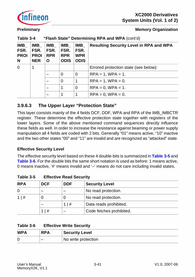
XC2000 DerivativesSystem Units (Vol. 1 of 2)
Memory OrganizationPreliminary
3.9.6.3 The Upper Layer “Protection State”This layer consists mainly of the 4 fields DCF, DDF, WPA and RPA of the IMB_IMBCTRregister. These determine the effective protection state together with registers of thelower layers. Some of the above mentioned command sequences directly influencethese fields as well. In order to increase the resistance against beaming or power supplymanipulation all 4 fields are coded with 2 bits. Generally “01” means active, “10” inactiveand the two other states “00” and “11” are invalid and are recognized as “attacked” state.
Effective Security LevelThe effective security level based on these 4 double-bits is summarized in Table 3-5 andTable 3-6. For the double bits the same short notation is used as before: 1 means active,0 means inactive, ‘#’ means invalid and ‘–’ means do not care including invalid states.
0 1 Errored protection state (see below):– 0 0 RPA = 1, WPA = 1.– 0 1 RPA = 1, WPA = 0.– 1 0 RPA = 0, WPA = 1.– 1 1 RPA = 0, WPA = 0.
Table 3-5 Effective Read SecurityRPA DCF DDF Security Level0 – – No read protection.1 | # 0 0 No read protection.
– 1 | # Data reads prohibited.1 | # – Code fetches prohibited.
Table 3-6 Effective Write SecurityWPA RPA Security Level0 – No write protection
Table 3-4 “Flash State” Determining RPA and WPA (cont’d)
IMB_FSR.PROIN
IMB_FSR.PROINER
IMB_FSR.RPRO
IMB_FSR.RPRODIS
IMB_FSR.WPRODIS
Resulting Security Level in RPA and WPA
User’s Manual 3-41 V1.0, 2007-06MemoryX2K, V1.1
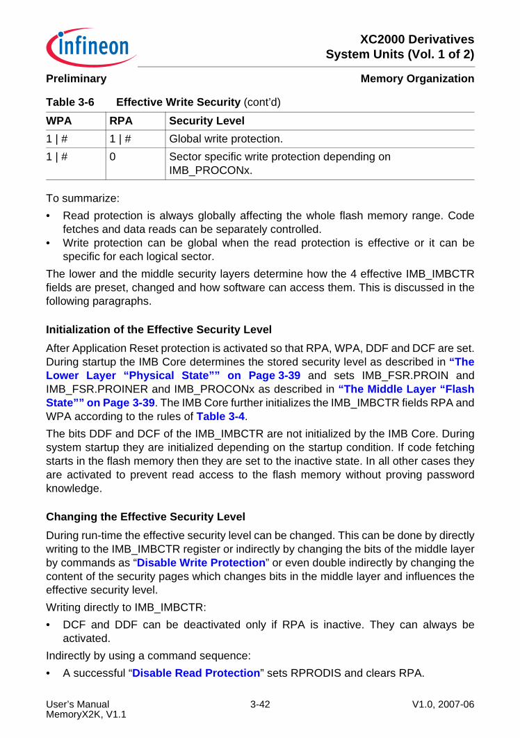
XC2000 DerivativesSystem Units (Vol. 1 of 2)
Memory OrganizationPreliminary
To summarize:• Read protection is always globally affecting the whole flash memory range. Code
fetches and data reads can be separately controlled.• Write protection can be global when the read protection is effective or it can be
specific for each logical sector.The lower and the middle security layers determine how the 4 effective IMB_IMBCTRfields are preset, changed and how software can access them. This is discussed in thefollowing paragraphs.
Initialization of the Effective Security LevelAfter Application Reset protection is activated so that RPA, WPA, DDF and DCF are set.During startup the IMB Core determines the stored security level as described in “TheLower Layer “Physical State”” on Page 3-39 and sets IMB_FSR.PROIN andIMB_FSR.PROINER and IMB_PROCONx as described in “The Middle Layer “FlashState”” on Page 3-39. The IMB Core further initializes the IMB_IMBCTR fields RPA andWPA according to the rules of Table 3-4.The bits DDF and DCF of the IMB_IMBCTR are not initialized by the IMB Core. Duringsystem startup they are initialized depending on the startup condition. If code fetchingstarts in the flash memory then they are set to the inactive state. In all other cases theyare activated to prevent read access to the flash memory without proving passwordknowledge.
Changing the Effective Security LevelDuring run-time the effective security level can be changed. This can be done by directlywriting to the IMB_IMBCTR register or indirectly by changing the bits of the middle layerby commands as “Disable Write Protection” or even double indirectly by changing thecontent of the security pages which changes bits in the middle layer and influences theeffective security level.Writing directly to IMB_IMBCTR:• DCF and DDF can be deactivated only if RPA is inactive. They can always be
activated.Indirectly by using a command sequence:• A successful “Disable Read Protection” sets RPRODIS and clears RPA.
1 | # 1 | # Global write protection.1 | # 0 Sector specific write protection depending on
IMB_PROCONx.
Table 3-6 Effective Write Security (cont’d)
WPA RPA Security Level
User’s Manual 3-42 V1.0, 2007-06MemoryX2K, V1.1
XC2000 DerivativesSystem Units (Vol. 1 of 2)
Memory OrganizationPreliminary
• A successful “Disable Write Protection” sets WPRODIS and clears WPA.• “Re-Enable Read/Write Protection” clears RPRODIS and WPRODIS and sets RPA
and WPA according to Table 3-4 depending on PROIN, PROINER and RPRO.Double indirect by changing security pages. After executing a command sequence thatchanged the content of a security page the IMB Core immediately reads back the pagesand determines all resulting security data as described for system startup in“Initialization of the Effective Security Level” on Page 3-42. The examples in“Protection Handling Examples” on Page 3-45 will show how this can be used forinstalling and removing protection or changing passwords.
3.9.6.4 Reaction on Protection ViolationIf software tries to violate the protection rules the following happens:• Reading data when read protection is effective: The bit IMB_FSR.PROER is set and
the Flash access trap can be triggered via the SCU if IMB_INTCTR.DPROTRP is 0.Default data is delivered.
• Fetching code when read protection is effective: the trap code “TRAP 15D” isdelivered instead.
• Programming or erasing memory ranges when they are write protected: PROER isset.
3.9.6.5 Layout of the Security PagesThe previous sections just mentioned the content of the security pages. This sectiondepicts their exact layout. Figure 3-8 depicts symbolically the layout of the securitypages 0 and 1.
User’s Manual 3-43 V1.0, 2007-06MemoryX2K, V1.1
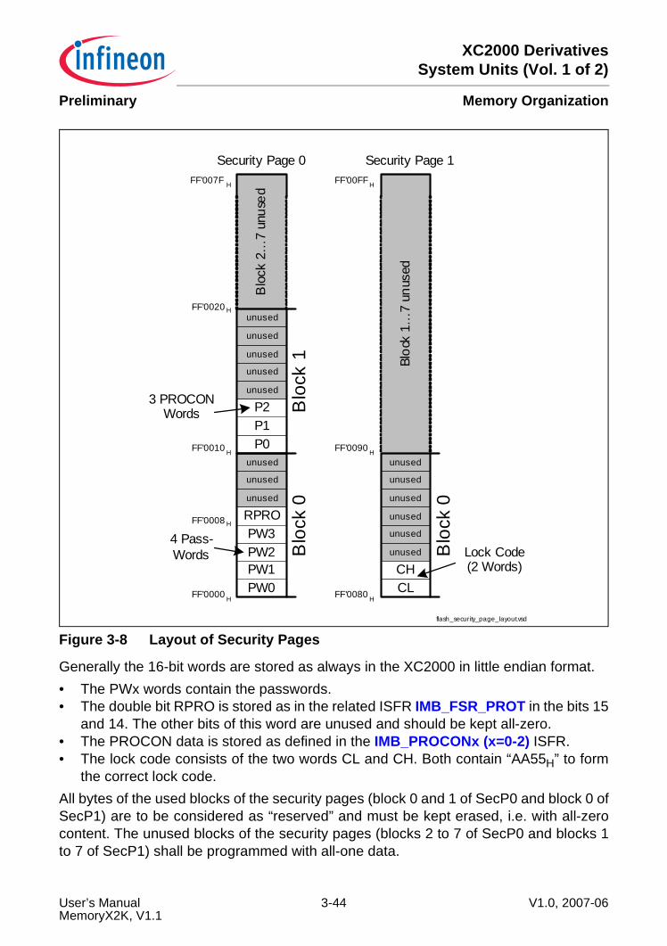
XC2000 DerivativesSystem Units (Vol. 1 of 2)
Memory OrganizationPreliminary
Figure 3-8 Layout of Security Pages
Generally the 16-bit words are stored as always in the XC2000 in little endian format.• The PWx words contain the passwords.• The double bit RPRO is stored as in the related ISFR IMB_FSR_PROT in the bits 15
and 14. The other bits of this word are unused and should be kept all-zero.• The PROCON data is stored as defined in the IMB_PROCONx (x=0-2) ISFR.• The lock code consists of the two words CL and CH. Both contain “AA55H” to form
the correct lock code.All bytes of the used blocks of the security pages (block 0 and 1 of SecP0 and block 0 ofSecP1) are to be considered as “reserved” and must be kept erased, i.e. with all-zerocontent. The unused blocks of the security pages (blocks 2 to 7 of SecP0 and blocks 1to 7 of SecP1) shall be programmed with all-one data.
Bloc
k 1…
7 un
used
Blo
ck 2
…7
unus
ed
CH
RPRO
FF'0080 HCL
Lock Code(2 Words)
Security Page 1
flash_security_page_layout.vsd
FF'0010 H
Security Page 0
FF'0000 H
4 Pass-Words
PW0PW1PW2PW3
3 PROCONWords
P0P1P2
FF'0008 H
FF'0020 HB
lock
0B
lock
1
unused
unused
unused
unused
unused
unused
unused
Blo
ck 0
unused
unused
unused
unused
unused
unused
FF'0090 H
FF'00FFHFF'007F H
unused
User’s Manual 3-44 V1.0, 2007-06MemoryX2K, V1.1
XC2000 DerivativesSystem Units (Vol. 1 of 2)
Memory OrganizationPreliminary
3.9.7 Protection Handling ExamplesSome examples on how to work with the protection system.
Delivery StateThe device is delivered in the “non-protected state”.Security page 1 is erased (so it does not contain the “lock code” AA55AA55H).Security page 0 is erased and so “invalid” but because SecP1 is erased this data isanyhow not evaluated. Only its content is copied into corresponding the registers.During startup the bits DDF and DCF are set depending on the start mode but as RPAand WPA are inactive all accesses to the flash memory are allowed.The data sectors of the flash memory are delivered in the erased state as well. All sectorscan be programmed. After uploading the software the customer can install write and readprotection.
First Time Password InstallationIn order to install a password generally the lock code in SecP1 has to be erased. In thiscase the code is not present.After that SecP0 must be erased with “Erase Security Page” in order to be able tochange RPRO. Erasing SecP0 clears RPRO to “00B” which is an invalid state. Afterfinishing the erase command the IMB Core restores the IMB_FSR and IMB_IMBCTRfields from the flash data.Because no lock code is present in SecP1 the invalid state of RPRO has no effect on theuser visible protection. Still all parts of the flash memory can be written.The second step is to program the information of SecP0 with the required securityinformation. Again the IMB Core reads immediately back the stored data and initializesthe security system. As SecP1 still does not contain the lock code the device stays in the“non-protected” mode.The security pages cannot be read directly by customer software. The data programmedinto SecP0 can therefore only be verified indirectly. The data of the RPRO and SnU fieldscan be checked by reading the IMB_PROCON and IMB_FSR registers. The passwordscan be verified with the command “Disable Read Protection”. If the password does notmatch the bit PROER is set. But because of the erased SecP1 the flash memory stayswritable. So after erasing SecP0 the correct password can be programmed again.After the SecP0 was verified successfully SecP1 gets programmed with the lock codeAA55AA55H which enables the security settings of SecP0.Because the password validation left RPRODIS set the command “Re-Enable Read/Write Protection” must be used to finally activate the new protection.
User’s Manual 3-45 V1.0, 2007-06MemoryX2K, V1.1
XC2000 DerivativesSystem Units (Vol. 1 of 2)
Memory OrganizationPreliminary
Changing Passwords or Security SettingsChanging the passwords is a delicate operation. The interrelation of the two securitypages must be kept in mind.Usually in the protected state the SecP1 contains the lock code. First write protectionmust be disabled with the correct passwords. Then the lock code in SecP1 is erased. Ifthis operation was successful PROIN will be cleared by the IMB Core. Now SecP0 canbe safely erased.From this point on the security pages are in the factory delivery state and the newpasswords and security settings can be installed as described above.Attention: The number of times a security page may be changed is noted in the
datasheet.
User’s Manual 3-46 V1.0, 2007-06MemoryX2K, V1.1
XC2000 DerivativesSystem Units (Vol. 1 of 2)
Memory OrganizationPreliminary
3.9.8 EEPROM EmulationThe flash memory of the XC2000 is used for three purposes:1. Storage of program code. Updates happen usually very seldom. The main criteria to
be fulfilled is a retention of the life-time of the product.2. Storage of constant data: this data is stored together with program code. So this data
is very seldom updated. Endurance is of no issue here but retention identical to thecode memory is required.
3. Data updated during run-time: this might be data with a very high frequency ofupdates like a mileage counter or access keys for key-less entry. Other data mightbe changed only in case of failures and other data might only be transferred fromRAM to non-volatile memory before the system is powered down.
Especially for the third type of data the non-volatile memory needs EEPROM likecharacteristics:• Fine program/erase granularity which is in EEPROMs typically 1 byte.• Higher endurance than the intrinsic endurance of flash cells.• Short program and erase duration per byte. Especially for storing data in an
emergency (e.g. power failure) short latencies might be required.A basic requirement for changing data during run-time is that code execution can stillresume, especially interrupt requests must still be serviced. This requirement is fulfilledin the XC2000 because all three flash modules work independently. If one is busy withprogram or erase then code can still be executed from the other two.The other requirements are more difficult to fulfill because the XC2000 does not have anEEPROM available but only the flash memory with the already frequently mentionedlimitations: big program/erase granularity, moderately long program/erase duration,limited cell endurance with reduced retention at high number of program/erase cycles,pages not isolated but affected by drain disturbs.In order to alleviate these effects on run-time storage of data software is used to emulateEEPROM. There is quite a number of algorithms for efficiently using flash memory asEEPROM. The following section describes one (the most simple) of these algorithms.It should be noted that the XC2000 does not offer the customer any hardware means forEEPROM emulation. All of the following must be realized by software.
3.9.8.1 The Traditional EEPROM EmulationThis algorithm was already used in the Pegasus devices. The key point is to solve thelimited endurance by storing data in N different physical places. In XC2000 the algorithmwould use N sequential pages or groups of pages. If data is currently stored in the page“x” then the next program happens to the page “(x+1) mod N”. The software typicallystores the current address in a table in RAM to avoid searching for the page at everyaccess.
User’s Manual 3-47 V1.0, 2007-06MemoryX2K, V1.1
XC2000 DerivativesSystem Units (Vol. 1 of 2)
Memory OrganizationPreliminary
In order to find the current data after boot-up every entry must be marked. Either itcontains a counter (from 0 to 2*N-1) or the old entries are invalidated by erasing the pageafter programming the new one.After boot-up the emulation driver software must recover this mapping information1). Thesame must happen in case of power-down modes that shut-down the main memory.As all involved pages are re-used cyclically the endurance from customer perspective isincreased by the factor N. N must be chosen high enough to fulfill endurance andretention requirements. Disturbs in the group of N pages are no issue because they incurat most N-1 disturbs before they get written with new data. Care must be taken howeverif one sector accommodates different groups of pages with different update behavior. Inthis case the updates of one group of pages could exceed the disturb limits of the othergroup. So generally one sector should be used only by one such EEPROM cyclic buffer.The algorithm keeps the old data until the new data is verified so power failure duringprogramming can only destroy the last update but the older data is still available. Thereare still some issues with power failure that need special treatment:• Power is cut during programming: the following boot-up might find an apparently
correctly programmed page. However the cells might be not fully programmed andthus have a much lower retention. The algorithm must detect this situation andfinalize the programming, e.g. with margin reads.
• Power is cut during erase: the same as above can happen. Data may appear aserased but the retention is lowered.
The algorithm can be improved to cover these cases as well. The easiest solution is touse margin reads to verify the program or erase steps.The main deficiency of the described algorithm is that the software designer is requiredto plan the use of the flash memory thoroughly. The user has to choose the correct valueof N. Then all data has to be allocated to pages. Data sharing one page should have asimilar or better identical update pattern (otherwise unchanged data is unnecessarilywritten). If one set of data does not fill a complete sector the available pages must bepossibly left unused because they might incur too many drain disturbs.There are other algorithms that try to alleviate these efforts by monitoring the flash usageand adapt automatically the assignment of data to flash cells.
1) This time must be taken into account for calculating the startup duration.
User’s Manual 3-48 V1.0, 2007-06MemoryX2K, V1.1
XC2000 DerivativesSystem Units (Vol. 1 of 2)
Memory OrganizationPreliminary
3.9.9 Interrupt GenerationLong lasting processes (these are mainly: program page, erase page, erase sector andmargin changes) set the IMB_FSR.BUSY flag of one flash module when accepting therequest and reset this flag after finishing the process. Software is required to poll thebusy flag in order to determine the end of the operation. In order to release the softwarefrom this burden an interrupt can be generated. If the interrupt is enabled byIMB_INTCTRL.IEN then all transitions from 1 to 0 of one of the 3 IMB_FSR.BUSY flagssend an interrupt request.The “Enter Page Mode” command sets BUSY only for around 100 clock cycles. It isusually not advisable to enable the interrupt for this command.The register IMB_INTCTR contains fields for the interrupt status “ISR”, an enable for theinterrupt request “IEN” and fields for clearing the status flag “ICLR” or setting if “ISET”. Itshould be noted that the interrupt request is only sent when ISR becomes 1 and IEN wasalready 1. No interrupt is sent when IEN becomes 1 when ISR was already 1 or both areset to 1 at the same time.
User’s Manual 3-49 V1.0, 2007-06MemoryX2K, V1.1
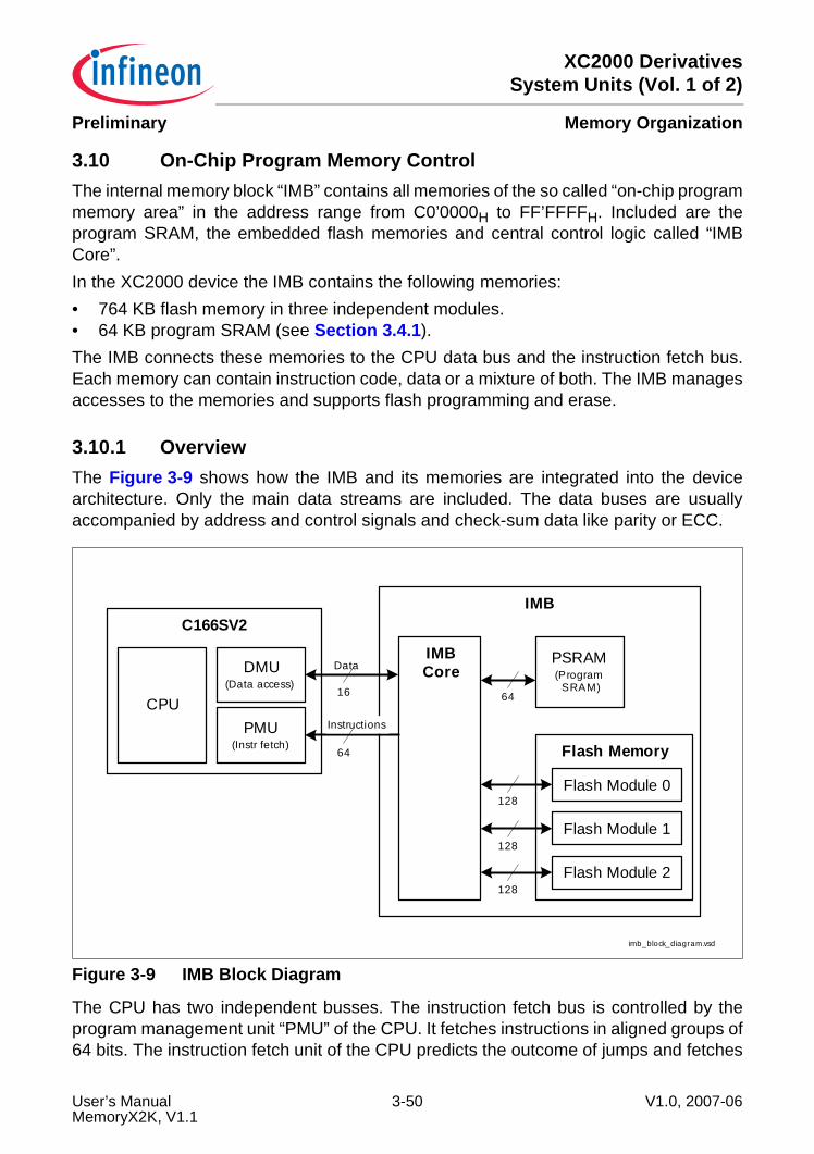
XC2000 DerivativesSystem Units (Vol. 1 of 2)
Memory OrganizationPreliminary
3.10 On-Chip Program Memory ControlThe internal memory block “IMB” contains all memories of the so called “on-chip programmemory area” in the address range from C0’0000H to FF’FFFFH. Included are theprogram SRAM, the embedded flash memories and central control logic called “IMBCore”.In the XC2000 device the IMB contains the following memories:• 764 KB flash memory in three independent modules.• 64 KB program SRAM (see Section 3.4.1).The IMB connects these memories to the CPU data bus and the instruction fetch bus.Each memory can contain instruction code, data or a mixture of both. The IMB managesaccesses to the memories and supports flash programming and erase.
3.10.1 OverviewThe Figure 3-9 shows how the IMB and its memories are integrated into the devicearchitecture. Only the main data streams are included. The data buses are usuallyaccompanied by address and control signals and check-sum data like parity or ECC.
Figure 3-9 IMB Block Diagram
The CPU has two independent busses. The instruction fetch bus is controlled by theprogram management unit “PMU” of the CPU. It fetches instructions in aligned groups of64 bits. The instruction fetch unit of the CPU predicts the outcome of jumps and fetches
IMB
Flash Memory
Flash Module 0
Flash Module 1
Flash Module 2
PSRAM(Program
SRAM)
IMBCoreData
Instructions
64
128
128
imb_block_diagram.vsd
128
16
64
C166SV2
PMU(Instr fetch)
DMU(Data access)
CPU
User’s Manual 3-50 V1.0, 2007-06MemoryX2K, V1.1
XC2000 DerivativesSystem Units (Vol. 1 of 2)
Memory OrganizationPreliminary
instructions on the predicted branch in advance. In case of a misprediction this interfacecan abort outstanding requests and continues fetching on the correct branch. As theCPU can consume up to one 32-bit instruction per clock cycle the performance of thisinterface determines the CPU performance.The data bus is controlled by the data management unit “DMU” of the CPU. It reads datain words of 16 bits. Write accesses address as well 16-bit words but additional byteenables allow changing single bytes.Because of the CPU’s “von Neumann” architecture data and instructions (and “specialfunction registers” to complete the list) share a common address range. Wheninstructions are used as data (e.g. when copying code from an IO interface to thePSRAM) they are accessed via the data bus. The pipelined behavior of the CPU cancause that code fetches and data accesses are requested simultaneously. The IMBtakes care that accesses can perform concurrently if they address different memories orflash modules.Additional connections of the IMB to central system control units exist. These are notshown in the block diagram.
User’s Manual 3-51 V1.0, 2007-06MemoryX2K, V1.1

XC2000 DerivativesSystem Units (Vol. 1 of 2)
Memory OrganizationPreliminary
3.10.2 Register InterfaceThe “IMB Registers” on Page 3-52 describes the special function registers of the IMB.In “System Control Registers” on Page 3-63 the special function registers thatinfluence the IMB but are not allocated to the IMB address range are described.
3.10.2.1 IMB RegistersThe section describes all IMB special function registers.
IMB ControlGlobal IMB control.Both IMB_IMBCTRL and IMB_IMBCTRH are reset by an Application Reset.The write access to both registers is controlled by the register security mechanism asdefined in the SCU chapter “Register Control” on Page 6-181. Please note that theregister write-protection is not activated automatically again after an access toIMB_IMBCTR because this happens only for SCU internal registers.
Table 3-7 Registers OverviewRegister Short Name
Register Long Name Offset Address
Page Number
IMB_IMBCTRL IMB Control Low FF FF00H Page 3-52IMB_IMBCTRH IMB Control High FF FF02H Page 3-54IMB_INTCTR Interrupt Control FF FF04H Page 3-55IMB_FSR_BUSY Flash State Busy FF FF06H Page 3-57IMB_FSR_OP Flash State Operations FF FF08H Page 3-57IMB_FSR_PROT Flash State Protection FF FF0AH Page 3-59IMB_MAR Margin FF FF0CH Page 3-61IMB_PROCON0 Protection Configuration 0 FF FF10H Page 3-62IMB_PROCON1 Protection Configuration 1 FF FF12H Page 3-62IMB_PROCON2 Protection Configuration 2 FF FF14H Page 3-62
IMB_IMBCTRL IMB Control Low ISFR (FF FF00H) Reset value: 558CH
15 14 13 12 11 10 9 8 7 6 5 4 3 2 1 0
DDF DCF - - - - - - - - DLCPF WSFLASH
rw rw - - - - - - - - rw rw
User’s Manual 3-52 V1.0, 2007-06MemoryX2K, V1.1
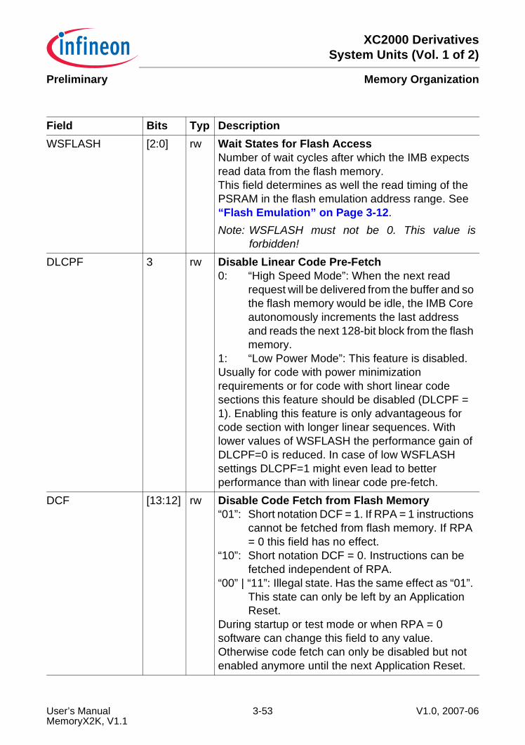
XC2000 DerivativesSystem Units (Vol. 1 of 2)
Memory OrganizationPreliminary
Field Bits Typ DescriptionWSFLASH [2:0] rw Wait States for Flash Access
Number of wait cycles after which the IMB expects read data from the flash memory.This field determines as well the read timing of the PSRAM in the flash emulation address range. See “Flash Emulation” on Page 3-12.Note: WSFLASH must not be 0. This value is
forbidden!DLCPF 3 rw Disable Linear Code Pre-Fetch
0: “High Speed Mode”: When the next read request will be delivered from the buffer and so the flash memory would be idle, the IMB Core autonomously increments the last address and reads the next 128-bit block from the flash memory.
1: “Low Power Mode”: This feature is disabled.Usually for code with power minimization requirements or for code with short linear code sections this feature should be disabled (DLCPF = 1). Enabling this feature is only advantageous for code section with longer linear sequences. With lower values of WSFLASH the performance gain of DLCPF=0 is reduced. In case of low WSFLASH settings DLCPF=1 might even lead to better performance than with linear code pre-fetch.
DCF [13:12] rw Disable Code Fetch from Flash Memory“01”: Short notation DCF = 1. If RPA = 1 instructions
cannot be fetched from flash memory. If RPA = 0 this field has no effect.
“10”: Short notation DCF = 0. Instructions can be fetched independent of RPA.
“00” | “11”: Illegal state. Has the same effect as “01”. This state can only be left by an Application Reset.
During startup or test mode or when RPA = 0 software can change this field to any value. Otherwise code fetch can only be disabled but not enabled anymore until the next Application Reset.
User’s Manual 3-53 V1.0, 2007-06MemoryX2K, V1.1

XC2000 DerivativesSystem Units (Vol. 1 of 2)
Memory OrganizationPreliminary
IMB control high word. The WPA and RPA fields are described in “Protection HandlingDetails” on Page 3-38.
DDF [15:14] rw Disable Data Read from Flash Memory“01”: Short notation DDF = 1. If RPA = 1 data cannot
be read from flash memory. If RPA = 0 this field has no effect.
“10”: Short notation DDF = 0. Data can be read independent of RPA.
“00” | “11”: Illegal state. Has the same effect as “01”. This state can only be left by an Application Reset.
During startup or test mode or when RPA = 0 software can change this field to any value. Otherwise data reads can only be disabled but not enabled anymore until the next Application Reset.
IMB_IMBCTRH IMB Control High ISFR (FF FF02H) Reset value: 0005H
15 14 13 12 11 10 9 8 7 6 5 4 3 2 1 0
PSPROT – – – – RPA WPA
rw – – – – rh rh
Field Bits Typ DescriptionWPA [1:0] rh Write Protection Activated
“01”: Short notation WPA = 1. The write protection of the flash memory is activated.
“10”: Short notation WPA = 0. The write protection is not activated.
“00” | “11”: Illegal state. Same effect as “01”. The illegal state can only be left by an Application Reset.
This field is only changed by the IMB Core. Software writes are ignored.
Field Bits Typ Description
User’s Manual 3-54 V1.0, 2007-06MemoryX2K, V1.1
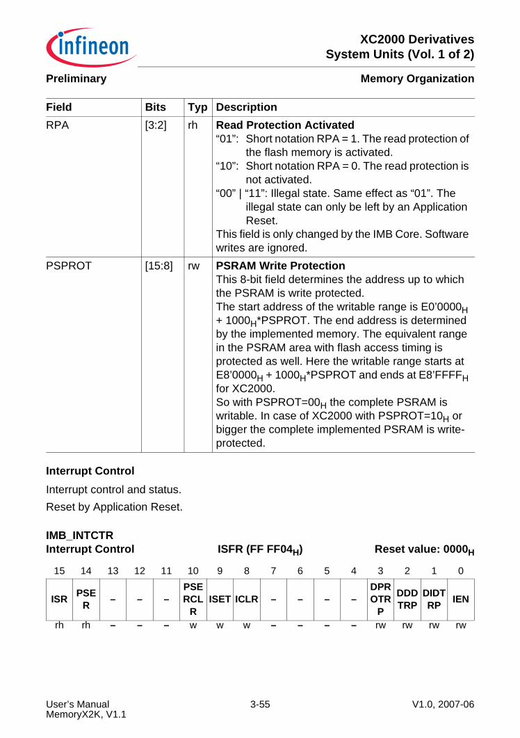
XC2000 DerivativesSystem Units (Vol. 1 of 2)
Memory OrganizationPreliminary
Interrupt ControlInterrupt control and status.Reset by Application Reset.
RPA [3:2] rh Read Protection Activated“01”: Short notation RPA = 1. The read protection of
the flash memory is activated.“10”: Short notation RPA = 0. The read protection is
not activated.“00” | “11”: Illegal state. Same effect as “01”. The
illegal state can only be left by an Application Reset.
This field is only changed by the IMB Core. Software writes are ignored.
PSPROT [15:8] rw PSRAM Write ProtectionThis 8-bit field determines the address up to which the PSRAM is write protected.The start address of the writable range is E0’0000H + 1000H*PSPROT. The end address is determined by the implemented memory. The equivalent range in the PSRAM area with flash access timing is protected as well. Here the writable range starts at E8’0000H + 1000H*PSPROT and ends at E8’FFFFH for XC2000.So with PSPROT=00H the complete PSRAM is writable. In case of XC2000 with PSPROT=10H or bigger the complete implemented PSRAM is write-protected.
IMB_INTCTR Interrupt Control ISFR (FF FF04H) Reset value: 0000H
15 14 13 12 11 10 9 8 7 6 5 4 3 2 1 0
ISR PSER – – –
PSERCL
RISET ICLR – – – –
DPROTR
P
DDDTRP
DIDTRP IEN
rh rh – – – w w w – – – – rw rw rw rw
Field Bits Typ Description
User’s Manual 3-55 V1.0, 2007-06MemoryX2K, V1.1
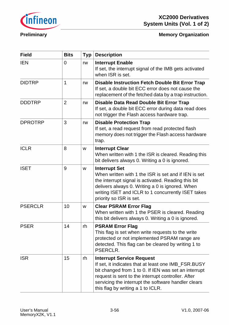
XC2000 DerivativesSystem Units (Vol. 1 of 2)
Memory OrganizationPreliminary
Field Bits Typ DescriptionIEN 0 rw Interrupt Enable
If set, the interrupt signal of the IMB gets activated when ISR is set.
DIDTRP 1 rw Disable Instruction Fetch Double Bit Error TrapIf set, a double bit ECC error does not cause the replacement of the fetched data by a trap instruction.
DDDTRP 2 rw Disable Data Read Double Bit Error TrapIf set, a double bit ECC error during data read does not trigger the Flash access hardware trap.
DPROTRP 3 rw Disable Protection TrapIf set, a read request from read protected flash memory does not trigger the Flash access hardware trap.
ICLR 8 w Interrupt ClearWhen written with 1 the ISR is cleared. Reading this bit delivers always 0. Writing a 0 is ignored.
ISET 9 w Interrupt SetWhen written with 1 the ISR is set and if IEN is set the interrupt signal is activated. Reading this bit delivers always 0. Writing a 0 is ignored. When writing ISET and ICLR to 1 concurrently ISET takes priority so ISR is set.
PSERCLR 10 w Clear PSRAM Error FlagWhen written with 1 the PSER is cleared. Reading this bit delivers always 0. Writing a 0 is ignored.
PSER 14 rh PSRAM Error FlagThis flag is set when write requests to the write protected or not implemented PSRAM range are detected. This flag can be cleared by writing 1 to PSERCLR.
ISR 15 rh Interrupt Service RequestIf set, it indicates that at least one IMB_FSR.BUSY bit changed from 1 to 0. If IEN was set an interrupt request is sent to the interrupt controller. After servicing the interrupt the software handler clears this flag by writing a 1 to ICLR.
User’s Manual 3-56 V1.0, 2007-06MemoryX2K, V1.1
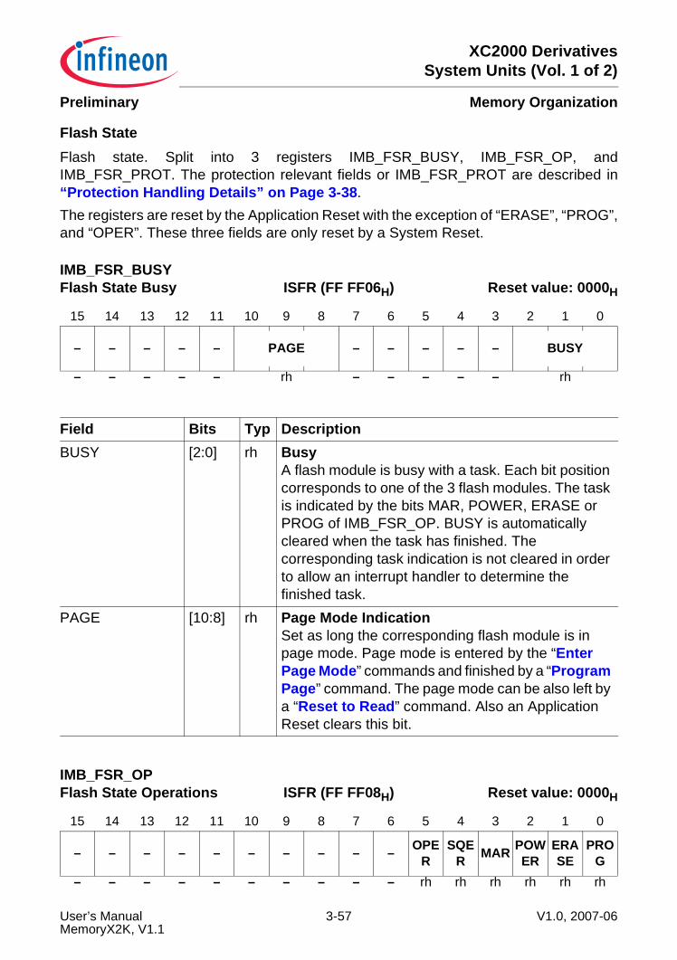
XC2000 DerivativesSystem Units (Vol. 1 of 2)
Memory OrganizationPreliminary
Flash StateFlash state. Split into 3 registers IMB_FSR_BUSY, IMB_FSR_OP, andIMB_FSR_PROT. The protection relevant fields or IMB_FSR_PROT are described in“Protection Handling Details” on Page 3-38.The registers are reset by the Application Reset with the exception of “ERASE”, “PROG”,and “OPER”. These three fields are only reset by a System Reset.
IMB_FSR_BUSY Flash State Busy ISFR (FF FF06H) Reset value: 0000H
15 14 13 12 11 10 9 8 7 6 5 4 3 2 1 0
– – – – – PAGE – – – – – BUSY
– – – – – rh – – – – – rh
Field Bits Typ DescriptionBUSY [2:0] rh Busy
A flash module is busy with a task. Each bit position corresponds to one of the 3 flash modules. The task is indicated by the bits MAR, POWER, ERASE or PROG of IMB_FSR_OP. BUSY is automatically cleared when the task has finished. The corresponding task indication is not cleared in order to allow an interrupt handler to determine the finished task.
PAGE [10:8] rh Page Mode IndicationSet as long the corresponding flash module is in page mode. Page mode is entered by the “Enter Page Mode” commands and finished by a “Program Page” command. The page mode can be also left by a “Reset to Read” command. Also an Application Reset clears this bit.
IMB_FSR_OP Flash State Operations ISFR (FF FF08H) Reset value: 0000H
15 14 13 12 11 10 9 8 7 6 5 4 3 2 1 0
– – – – – – – – – – OPER
SQER MAR POW
ERERASE
PROG
– – – – – – – – – – rh rh rh rh rh rh
User’s Manual 3-57 V1.0, 2007-06MemoryX2K, V1.1
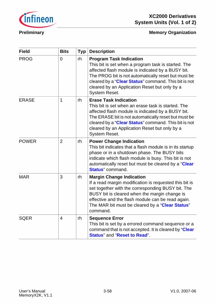
XC2000 DerivativesSystem Units (Vol. 1 of 2)
Memory OrganizationPreliminary
Field Bits Typ DescriptionPROG 0 rh Program Task Indication
This bit is set when a program task is started. The affected flash module is indicated by a BUSY bit. The PROG bit is not automatically reset but must be cleared by a “Clear Status” command. This bit is not cleared by an Application Reset but only by a System Reset.
ERASE 1 rh Erase Task IndicationThis bit is set when an erase task is started. The affected flash module is indicated by a BUSY bit. The ERASE bit is not automatically reset but must be cleared by a “Clear Status” command. This bit is not cleared by an Application Reset but only by a System Reset.
POWER 2 rh Power Change IndicationThis bit indicates that a flash module is in its startup phase or in a shutdown phase. The BUSY bits indicate which flash module is busy. This bit is not automatically reset but must be cleared by a “Clear Status” command.
MAR 3 rh Margin Change IndicationIf a read margin modification is requested this bit is set together with the corresponding BUSY bit. The BUSY bit is cleared when the margin change is effective and the flash module can be read again. The MAR bit must be cleared by a “Clear Status” command.
SQER 4 rh Sequence ErrorThis bit is set by a errored command sequence or a command that is not accepted. It is cleared by “Clear Status” and “Reset to Read”.
User’s Manual 3-58 V1.0, 2007-06MemoryX2K, V1.1
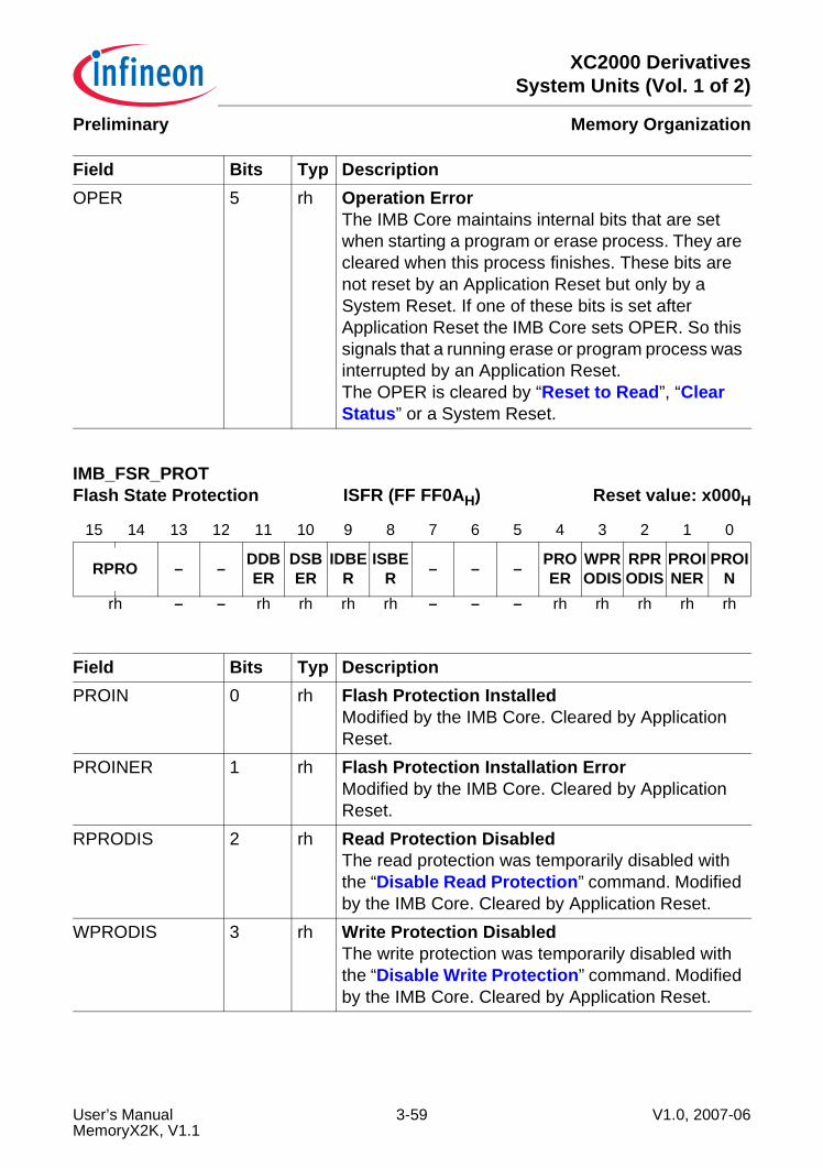
XC2000 DerivativesSystem Units (Vol. 1 of 2)
Memory OrganizationPreliminary
OPER 5 rh Operation ErrorThe IMB Core maintains internal bits that are set when starting a program or erase process. They are cleared when this process finishes. These bits are not reset by an Application Reset but only by a System Reset. If one of these bits is set after Application Reset the IMB Core sets OPER. So this signals that a running erase or program process was interrupted by an Application Reset.The OPER is cleared by “Reset to Read”, “Clear Status” or a System Reset.
IMB_FSR_PROT Flash State Protection ISFR (FF FF0AH) Reset value: x000H
15 14 13 12 11 10 9 8 7 6 5 4 3 2 1 0
RPRO – – DDBER
DSBER
IDBER
ISBER – – – PRO
ERWPRODIS
RPRODIS
PROINER
PROIN
rh – – rh rh rh rh – – – rh rh rh rh rh
Field Bits Typ DescriptionPROIN 0 rh Flash Protection Installed
Modified by the IMB Core. Cleared by Application Reset.
PROINER 1 rh Flash Protection Installation ErrorModified by the IMB Core. Cleared by Application Reset.
RPRODIS 2 rh Read Protection DisabledThe read protection was temporarily disabled with the “Disable Read Protection” command. Modified by the IMB Core. Cleared by Application Reset.
WPRODIS 3 rh Write Protection DisabledThe write protection was temporarily disabled with the “Disable Write Protection” command. Modified by the IMB Core. Cleared by Application Reset.
Field Bits Typ Description
User’s Manual 3-59 V1.0, 2007-06MemoryX2K, V1.1
XC2000 DerivativesSystem Units (Vol. 1 of 2)
Memory OrganizationPreliminary
Margin ControlRead margin control. Each field corresponds to one flash module. A hard read 0 detectsnot completely erased cells. These are read as “1”. A hard read 1 detects not completelyprogrammed cells. These are read as “0”. Read margin changes are caused by thecommand sequence “Change Read Margin”. The resulting read margin is reflected inthis status register.The command sequences “Program Page”, “Erase Sector”, “Erase Page” and “EraseSecurity Page” resets the read margin back to “normal”. The same happens in case ofa flash wake-up.Reset by Application Reset.
PROER 4 rh Protection ErrorSet by a violation of the installed protection. Reset by the “Clear Status” and “Reset to Read” commands or an Application Reset.
ISBER 8 rh Instruction Fetch Single Bit ErrorSet if during instruction fetch a single-bit ECC error was detected (and corrected). Reset by “Clear Status” or “Reset to Read” commands or an Application Reset.
IDBER 9 rh Instruction Fetch Double Bit ErrorSet if during instruction fetch a double-bit ECC error was detected (and not corrected). Reset by “Clear Status” or “Reset to Read” commands or an Application Reset.
DSBER 10 rh Data Read Single Bit ErrorSame as ISBER for data reads.
DDBER 11 rh Data Read Double Bit ErrorSame as IDBER for data reads.
RPRO [15:14] rh Read Protection ConfigurationThis field is copied by the IMB Core from the corresponding field in the security page 0. After Application Reset read protection is activated.
Field Bits Typ Description
User’s Manual 3-60 V1.0, 2007-06MemoryX2K, V1.1
XC2000 DerivativesSystem Units (Vol. 1 of 2)
Memory OrganizationPreliminary
Protection ConfigurationProtection configuration register of each implemented flash module. In XC2000PROCON0, PROCON1 and PROCON2 are implemented. PROCON0 is describedbelow. PROCON1 (at address FF’0012H) and PROCON2 (at address FF’F014H) havethe same functionality for the other two flash modules. The logical sector numbering isdepicted in Figure 3-6.Each bit of the PROCONs is related to a logical sector. If it is cleared the write access tothe corresponding logical sector (this means to the range of physical sectors) is lockedunder the conditions that are documented in “Protection Handling Details” onPage 3-38. The PROCON registers are exclusively modified by the IMB Core.Reset by Application Reset.
IMB_MAR Margin Control ISFR (FF FF0CH) Reset value: 0000H
15 14 13 12 11 10 9 8 7 6 5 4 3 2 1 0
– – – – – – – HREAD2 HREAD1 HREAD0
– – – – – – – rh rh rh
Field Bits Typ DescriptionHREAD0 [2:0] rh Hard Read 0
Active read margin of flash module 0.“000”:Normal read.“001”:Hard read 0.“010”: Alternate hard read 0 (usually harder than
001).“101”:Hard read 1.“110”: Alternate hard read 1 (usually harder than
101).other codes:Reserved.
HREAD1 [5:3] rh Hard Read 1Same for flash module 1.
HREAD2 [8:6] rh Hard Read 2Same for flash module 2.
User’s Manual 3-61 V1.0, 2007-06MemoryX2K, V1.1
XC2000 DerivativesSystem Units (Vol. 1 of 2)
Memory OrganizationPreliminary
IMB_PROCONx (x=0-2) Protection Configuration. ISFR (FF FF10H+2*x) Reset value: 0000H
15 14 13 12 11 10 9 8 7 6 5 4 3 2 1 0
– – – – – – S9U S8U S7U S6U S5U S4U S3U S2U S1U S0U
– – – – – – rh rh rh rh rh rh rh rh rh rh
Field Bits Typ DescriptionSsU (s=0-9) s rh Sector 0 to 9 Unlock
s: Logical sector s of flash module 0 is write-protected.
User’s Manual 3-62 V1.0, 2007-06MemoryX2K, V1.1
XC2000 DerivativesSystem Units (Vol. 1 of 2)
Memory OrganizationPreliminary
3.10.2.2 System Control RegistersThese registers are used to wakeup and shutdown parts of the memory sub-system.
Memory Kernel ConfigurationThis register controls the shutdown request of the processor sub-system units DMU,PMU, IMB and EBC (see “Processor Sub-System Shutdown” on Page 3-67). Thelayout of this register is identical to the other KSCCFGs but only the field COMCFG maybe used. Two values of this field might be used: 00B means that the “Clock-off Mode”does not trigger a shutdown of the processor sub-system. This may be used only if thesystem clock of DMP_1 is not disabled in the “Clock-off Mode”.The second useful value is 10B. This value must be used in all cases when the “Clock-off Mode” is accompanied by disabling the system clock of the DMP_1. In this case thesequence described in “Processor Sub-System Shutdown” on Page 3-67 must beperformed.This register gets is reset by an Application Reset. Attention: the reset value ofCOMCFG is 00B.
Table 3-8 Registers Address SpaceModule Base Address End Address NoteSCU 0000H 0FFFH SCU Module
Table 3-9 Registers OverviewRegister Short Name
Register Long Name Offset Address
Page Number
MEM_KSCCFG Memory Kernel Control F012H Page 3-63FL_KSCCFG Flash Kernel Control FE22H Page 3-64
MEM_KSCCFG Memory Kernel State Con ESFR (F012H/06H) Reset Value: 0001H
15 14 13 12 11 10 9 8 7 6 5 4 3 2 1 0
BPCOM – COMCFG – – – – – – – – 1
w – rw – – – – – – – – rw
Field Bits Type Description1 0 rw Has to be written to 1.
User’s Manual 3-63 V1.0, 2007-06MemoryX2K, V1.1
XC2000 DerivativesSystem Units (Vol. 1 of 2)
Memory OrganizationPreliminary
Flash Kernel ConfigurationThis register controls the power-down request of the flash module. When configuring thisregister care must be taken not to enable a powered-down flash module when theoperating voltage is not sufficient. In this case all CFG fields should contain 10B.This register is reset by an Application Reset.
COMCFG [13:12] rw Clock Off Mode ConfigurationThis bit field defines if the shutdown request is activated in clock-off mode.If COMCFG[13] is 1 the shutdown request is activated in clock-off mode (i.e. CR = 10).COMCFG[12] has no functionality.
BPCOM 15 w Bit Protection for COMCFGThis bit enables the write access to the bit field COMCFG. It always reads 0. It is only active during the write access cycle.0 The bit field COMCFG is not changed.1 The bit field COMCFG is updated with the
written value.
FL_KSCCFG Flash Kernel State Con. SFR (FE22H/11H) Reset Value: 0001H
15 14 13 12 11 10 9 8 7 6 5 4 3 2 1 0
BPCOM – COMCFG BP
SUM – SUMCFG BPNOM – NOMCFG –
BPMODEN
MODEN
w – rw w – rw w – rw – w rw
Field Bits Type DescriptionMODEN 0 rw Module Enable
This bit can directly set the power-down request.0 The power-down request is activated.1 This field has no effect.
Field Bits Type Description
User’s Manual 3-64 V1.0, 2007-06MemoryX2K, V1.1
XC2000 DerivativesSystem Units (Vol. 1 of 2)
Memory OrganizationPreliminary
BPMODEN 1 w Bit Protection for MODENThis bit enables the write access to the bit MODEN. It always reads 0. It is only active during the write access cycle.0 The bit MODEN is not changed.1 The bit MODEN is updated with the written
value.NOMCFG [5:4] rw Normal Operation Mode Configuration
This bit field defines if the power-down request is activated in normal operation mode.If NOMCFG[5] is 1 the power-down request is activated in normal mode (i.e. CR = 00 or 11).NOMCFG[4] has no functionality.
BPNOM 7 w Bit Protection for NOMCFGThis bit enables the write access to the bit field NOMCFG. It always reads 0. It is only active during the write access cycle.0 The bit field NOMCFG is not changed.1 The bit field NOMCFG is updated with the
written value.SUMCFG [9:8] rw Suspend Mode Configuration
This bit field defines if the power-down request is activated in suspend mode (which makes only sense if it is activated in normal mode as well).If SUMCFG[9] is 1 the power-down request is activated in shutdown mode (i.e. CR = 01).SUMCFG[8] has no functionality.
BPSUM 11 w Bit Protection for SUMCFGThis bit enables the write access to the bit field SUMCFG. It always reads 0. It is only active during the write access cycle.0 The bit field SUMCFG is not changed.1 The bit field SUMCFG is updated with the
written value.
Field Bits Type Description
User’s Manual 3-65 V1.0, 2007-06MemoryX2K, V1.1
XC2000 DerivativesSystem Units (Vol. 1 of 2)
Memory OrganizationPreliminary
COMCFG [13:12] rw Clock Off Mode ConfigurationThis bit field defines if the power-down request is activated in clock-off mode.If COMCFG[13] is 1 the power-down request is activated in clock-off mode (i.e. CR = 10).COMCFG[12] has no functionality.
BPCOM 15 w Bit Protection for COMCFGThis bit enables the write access to the bit field COMCFG. It always reads 0. It is only active during the write access cycle.0 The bit field COMCFG is not changed.1 The bit field COMCFG is updated with the
written value.
Field Bits Type Description
User’s Manual 3-66 V1.0, 2007-06MemoryX2K, V1.1
XC2000 DerivativesSystem Units (Vol. 1 of 2)
Memory OrganizationPreliminary
3.10.3 Startup, ShutdownThis section describes only shortly the shutdown and wake-up of the memory andprocessor sub-system. The use of this functionality is delicate and should be done witha software low-level driver according to Infineon recommendations.
3.10.3.1 Processor Sub-System ShutdownThe IMB with its memories PSRAM and the Flash memory is — from a programmerspoint of view — part of the processor sub-system. This contains additionally the CPUwith its memories, the DMU, the PMU, and the EBC. All these modules must be active(i.e. have a sufficient power supply and a running clock) to execute software.Consequently, their shutdown is controlled by a common KSCCFG calledMEM_KSCCFG (see Page 3-63).Before stopping the system clock or performing a power mode change the completeprocessor sub-system must be shutdown cleanly. This requires the following steps:• The CPU executes the IDLE instruction. This instruction cleans up the processor
pipeline and the CPU stops fetching instructions. After that the idle state is reportedto the system control unit specifically the PSC (see “Power State Controller (PSC)”on Page 6-128).
• The PSC must be configured so that — triggered by the IDLE — it performs asequence A transition. The sequence A entry triggers the “Clock-off Mode” requestby the GSC.
• The MEM_KSCCFG.COMCFG must be set to 10B so that the “Clock-off Mode”request of the GSC activates the shutdown request of the processor sub-systemmodules DMU, PMU, IMB and EBC. These acknowledge the request after finishingall outstanding tasks.
• The PSC can after that disable the system clock of DMP_1.The system control unit must not be configured to disable the system clock withoutperforming this sequence. The danger is that the clock is switched off before the lasttasks of the processor sub-system have finished. Mainly affected are the following longerlasting tasks:• Write accesses to the PSRAM: the last write access could be dropped.• Longer lasting processes in the Flash (e.g. erase sector, program page, …).• Write accesses via the EBC (e.g. to slow external memories): switching off the clock
while the external bus is active could even lead to timing violations at externalmemories with loss of data.
The details of the registers MEM_KSCCFG and the FL_KSCCFG are described in“System Control Registers” on Page 3-63.
User’s Manual 3-67 V1.0, 2007-06MemoryX2K, V1.1
XC2000 DerivativesSystem Units (Vol. 1 of 2)
Memory OrganizationPreliminary
3.10.3.2 Flash Module Power-DownBefore the power supply voltage of the IMB is reduced below 1.5 V the flash arrays mustbe powered down. The SCU controls the flash power-down with a dedicated kernel statecontrol register, the FL_KSCCFG. The flash power-down is requested by the SCU whenFL_KSCCFG.MODEN is 0 (the flash is disabled) or in case of a global clock-off modewhen the field FL_KSCCFG.COMCFG contains “10” or “11”. If the MSB of the SUMCFGor NOMCFG is 1 the flash power-down can also be requested in normal mode orsuspend mode.A power-down request by the SCU is forwarded by the IMB Core to all flash modules.The rest of the IMB is not affected by a flash power-down. So the device can continueoperation with the PSRAM. The IMB Core waits until all running processes have finishedin the flash modules before it acknowledges the power-down request. If the IMB Corehas received the beginning of a command sequence and is waiting for the rest whenreceiving the power-down request it resets it command interpreter and performs a“Reset to Read”. All accesses arriving after or with the power down request are ignored(read accesses return default data as defined for not-implemented memory ranges —see Table 3-10 “IMB Error Reporting” on Page 3-69). Accesses arriving after or witha power down request should be considered as system control failure. Either the SCUhardware or its low-level drivers must ensure that this case does not happen.
User’s Manual 3-68 V1.0, 2007-06MemoryX2K, V1.1
XC2000 DerivativesSystem Units (Vol. 1 of 2)
Memory OrganizationPreliminary
3.10.4 Error Reporting SummaryThe Table 3-10 summarizes the types of detected errors and the possible reactions.
Table 3-10 IMB Error ReportingError ReactionData read from PSRAM with parity error. If PECON.PEENPS:
HW trap (see Section 3.12).Instruction fetch from PSRAM with parity error.
If PECON.PEENPS:HW trap (see Section 3.12).
Data read from flash memory with single bit error.
Silently corrected. Bit IMB_FSR.DSBER set.
Data read from flash memory with double bit error.
Bit IMB_FSR.DDBER set.If IMB_INTCTR.DDDTRP = 0:Flash access trap (see Section 6.11.4) and default data is delivered.
Instruction fetch from flash memory with single bit error.
Silently corrected. Bit IMB_FSR.ISBER set.
Instruction fetch from flash memory with double bit error.
Bit IMB_FSR.IDBER set.If IMB_INTCTR.DIDTRP = 0:“TRAP 15D” delivered instead of corrupted data.
Data read from protected flash memory. IMB_FSR.PROER set.If IMB_INTCTR.DPROTRP = 0:Flash access trap (see Section 6.11.4) and default data is delivered.
Instruction fetch from protected flash memory.
“TRAP 15D” delivered.
Program/erase request of write protected flash range.
Only bit PROER in IMB_FSR set.
Data read or instruction fetch from busy flash memory.
Read access stalled until end of busy state.
Instruction fetch from ISFR addresses. Default data (“TRAP 15D”) delivered.Data read from not implemented ISFRs. Default data delivered.Data writes to not implemented ISFRs. Silently ignored.Data read from not implemented address range.
Unpredictable. Mirrored data from other memories might be returned or default values.
User’s Manual 3-69 V1.0, 2007-06MemoryX2K, V1.1
XC2000 DerivativesSystem Units (Vol. 1 of 2)
Memory OrganizationPreliminary
3.11 Data Retention MemoriesThis section describes the usage of the two special purpose data memories Stand-ByRAM (SBRAM) and Marker Memory (MKMEM). Both are supplied by the wake-up powerdomain (DMP_M) and retain their data while the system power domain (DMP_1) isswitched off.
Instruction fetch from not implemented address range.
Unpredictable. Mirrored data from other memories might be returned or default values.
Data written to not implemented PSRAM or write protected PSRAM address range (both determined by IMB_IMBCTR.PSPROT).
Bit IMB_INTCTR.PSER set.Flash access trap (see Section 6.11.4) and no data is changed in the PSRAM.
Program or erase command targeting not implemented flash memory.
Unpredictable. Access is ignored or mirrored into implemented flash memory1).
Data read from powered-down flash modules.
Considered as access to not-implemented memory range. Default data or data from implemented flash modules will be returned.
Instruction fetch from powered-down flash modules.
Considered as access to not-implemented memory range. Default data (“TRAP 15D”) will be returned or data from implemented flash modules.
Program or erase command targeting powered-down flash modules.
Silently ignored.
Shutdown or power-down request received while the command sequence interpreter is waiting for the last words of a command sequence.
The command interpreter is reset and a “Reset to Read” command sequence is executed.
1) The flash protection can not be by-passed by accessing the reserved memory ranges.
Table 3-10 IMB Error Reporting (cont’d)
Error Reaction
User’s Manual 3-70 V1.0, 2007-06MemoryX2K, V1.1
XC2000 DerivativesSystem Units (Vol. 1 of 2)
Memory OrganizationPreliminary
3.11.1 Stand-By RAM AccessesThe SBRAM is not mapped into the address range of the processor. All accesses aredone via the 4 SFRs SBRAM_WADD, SBRAM_RADD, SBRAM_DATA0 andSBRAM_DATA1. The following access options exist:• Write without automatic increment of the write address pointer:
The SW has to write the target address first to WADD and then the data to DATA0.The data written to DATA0 is transferred to the indicated address in the SBRAM if (atleast) the lower byte of DATA0 is written. If DATA0 is written again the same addressin SBRAM is used for data storage. Bit WADD.MOD is cleared by a write access toDATA0.
• Write with automatic increment of the write address pointer:The SW has to write the first target address to WADD and thereafter the data blockcan be written word by word to DATA1. The data written to DATA1 is transferred tothe indicated address in the SBRAM if (at least) the lower byte of SRDR1 is written.In parallel to the data storage in the SBRAM, the write address pointer WADD.WPTRis automatically incremented by 1 (one word) for the next data to be stored. Theaddress pointer automatically does a wrap-around after reaching its maximum valueand in this case, bit WADD.WA is set. Bit WADD.MOD is set by a write access toDATA1.
• Read without automatic increment of the read address pointer:The SW has to write the target address first to RADD and then can read the data fromDATA0. If DATA0 is read again the same address in SBRAM is read out. BitRADD.MOD is cleared by a read access to DATA0.
• Read with automatic increment of the read address pointer:The SW has to write the first target address to RADD and can then read the datablock word by word from DATA1. In parallel to the read action from SBRAM, the readaddress pointer RADD.RPTR is automatically incremented by 1 (one word) for thenext data to be read. The address pointer automatically does a wrap-around afterreaching its maximum value and in this case, bit RADD.WA is set. Bit RADD.MOD isset by a read access to DATA1.
The automatic increment accesses allow performing back-to-back data writes andreads.Note: Because read accesses to SBRAM_DATA0 and SBRAM_DATA1 return the value
that has been pre-read upon the most recent update of register SBRAM_RADD,any data written to location @SBRAM_RADD can only be read back afterSBRAM_RADD has been updated with the very same address (either explicitly bywriting to it or implicitly via the auto-increment function). Generally when switchingfrom write to read accesses SBRAM_RADD should be written again beforereading SBRAM_DATAx.
User’s Manual 3-71 V1.0, 2007-06MemoryX2K, V1.1
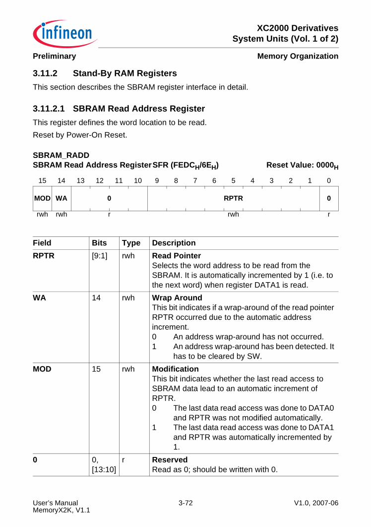
XC2000 DerivativesSystem Units (Vol. 1 of 2)
Memory OrganizationPreliminary
3.11.2 Stand-By RAM RegistersThis section describes the SBRAM register interface in detail.
3.11.2.1 SBRAM Read Address RegisterThis register defines the word location to be read.Reset by Power-On Reset.
SBRAM_RADD SBRAM Read Address RegisterSFR (FEDCH/6EH) Reset Value: 0000H
15 14 13 12 11 10 9 8 7 6 5 4 3 2 1 0
MOD WA 0 RPTR 0
rwh rwh r rwh r
Field Bits Type DescriptionRPTR [9:1] rwh Read Pointer
Selects the word address to be read from the SBRAM. It is automatically incremented by 1 (i.e. to the next word) when register DATA1 is read.
WA 14 rwh Wrap AroundThis bit indicates if a wrap-around of the read pointer RPTR occurred due to the automatic address increment.0 An address wrap-around has not occurred.1 An address wrap-around has been detected. It
has to be cleared by SW.MOD 15 rwh Modification
This bit indicates whether the last read access to SBRAM data lead to an automatic increment of RPTR.0 The last data read access was done to DATA0
and RPTR was not modified automatically.1 The last data read access was done to DATA1
and RPTR was automatically incremented by 1.
0 0,[13:10]
r ReservedRead as 0; should be written with 0.
User’s Manual 3-72 V1.0, 2007-06MemoryX2K, V1.1
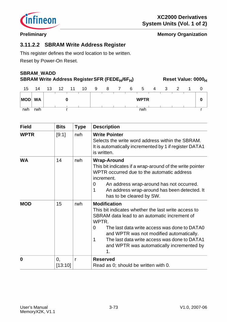
XC2000 DerivativesSystem Units (Vol. 1 of 2)
Memory OrganizationPreliminary
3.11.2.2 SBRAM Write Address RegisterThis register defines the word location to be written.Reset by Power-On Reset.
SBRAM_WADD SBRAM Write Address RegisterSFR (FEDEH/6FH) Reset Value: 0000H
15 14 13 12 11 10 9 8 7 6 5 4 3 2 1 0
MOD WA 0 WPTR 0
rwh rwh r rwh r
Field Bits Type DescriptionWPTR [9:1] rwh Write Pointer
Selects the write word address within the SBRAM.It is automatically incremented by 1 if register DATA1 is written.
WA 14 rwh Wrap-AroundThis bit indicates if a wrap-around of the write pointer WPTR occurred due to the automatic address increment.0 An address wrap-around has not occurred.1 An address wrap-around has been detected. It
has to be cleared by SW.MOD 15 rwh Modification
This bit indicates whether the last write access to SBRAM data lead to an automatic increment of WPTR.0 The last data write access was done to DATA0
and WPTR was not modified automatically.1 The last data write access was done to DATA1
and WPTR was automatically incremented by 1.
0 0,[13:10]
r ReservedRead as 0; should be written with 0.
User’s Manual 3-73 V1.0, 2007-06MemoryX2K, V1.1
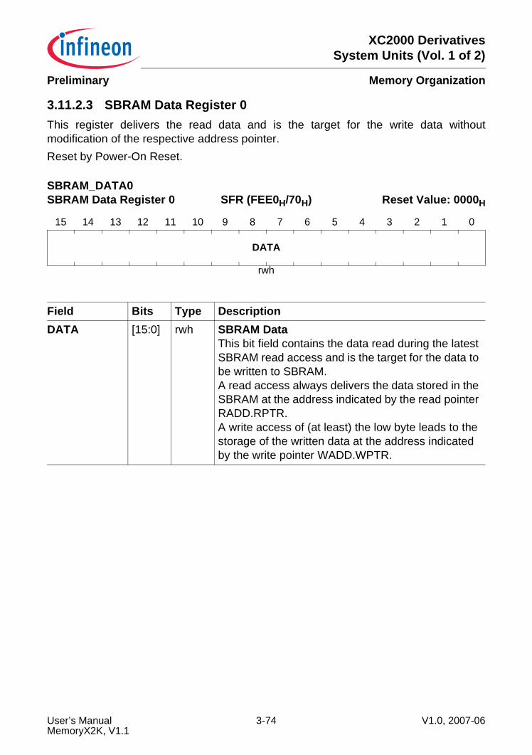
XC2000 DerivativesSystem Units (Vol. 1 of 2)
Memory OrganizationPreliminary
3.11.2.3 SBRAM Data Register 0This register delivers the read data and is the target for the write data withoutmodification of the respective address pointer.Reset by Power-On Reset.
SBRAM_DATA0 SBRAM Data Register 0 SFR (FEE0H/70H) Reset Value: 0000H
15 14 13 12 11 10 9 8 7 6 5 4 3 2 1 0
DATA
rwh
Field Bits Type DescriptionDATA [15:0] rwh SBRAM Data
This bit field contains the data read during the latest SBRAM read access and is the target for the data to be written to SBRAM.A read access always delivers the data stored in the SBRAM at the address indicated by the read pointer RADD.RPTR.A write access of (at least) the low byte leads to the storage of the written data at the address indicated by the write pointer WADD.WPTR.
User’s Manual 3-74 V1.0, 2007-06MemoryX2K, V1.1

XC2000 DerivativesSystem Units (Vol. 1 of 2)
Memory OrganizationPreliminary
3.11.2.4 SBRAM Data Register 1This register delivers the read data and is the target for the write data with modificationof the respective pointer.Reset by Power-On Reset.
SBRAM_DATA1 SBRAM Data Register 1 SFR (FEE2H/71H) Reset Value: 0000H
15 14 13 12 11 10 9 8 7 6 5 4 3 2 1 0
DATA
rwh
Field Bits Type DescriptionDATA [15:0] rwh SBRAM Data
This bit field contains the data read during the latest SBRAM read access and is the target for the data to be written to SBRAM.A write access of (at least) the low byte leads to the storage of the written data at the address indicated by the write pointer WADD.WPTR.A read access always delivers the data stored in the SBRAM at the address indicated by the read pointer RADD.RPTR.
User’s Manual 3-75 V1.0, 2007-06MemoryX2K, V1.1
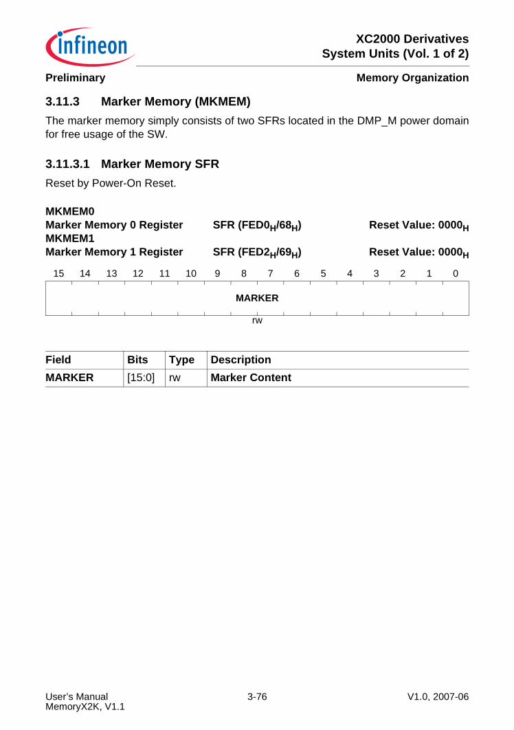
XC2000 DerivativesSystem Units (Vol. 1 of 2)
Memory OrganizationPreliminary
3.11.3 Marker Memory (MKMEM)The marker memory simply consists of two SFRs located in the DMP_M power domainfor free usage of the SW.
3.11.3.1 Marker Memory SFRReset by Power-On Reset.
MKMEM0 Marker Memory 0 Register SFR (FED0H/68H) Reset Value: 0000HMKMEM1Marker Memory 1 Register SFR (FED2H/69H) Reset Value: 0000H
15 14 13 12 11 10 9 8 7 6 5 4 3 2 1 0
MARKER
rw
Field Bits Type DescriptionMARKER [15:0] rw Marker Content
User’s Manual 3-76 V1.0, 2007-06MemoryX2K, V1.1
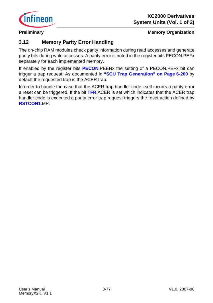
XC2000 DerivativesSystem Units (Vol. 1 of 2)
Memory OrganizationPreliminary
3.12 Memory Parity Error HandlingThe on-chip RAM modules check parity information during read accesses and generateparity bits during write accesses. A parity error is noted in the register bits PECON.PEFxseparately for each implemented memory.If enabled by the register bits PECON.PEENx the setting of a PECON.PEFx bit cantrigger a trap request. As documented in “SCU Trap Generation” on Page 6-200 bydefault the requested trap is the ACER trap.In order to handle the case that the ACER trap handler code itself incurrs a parity errora reset can be triggered. If the bit TFR.ACER is set which indicates that the ACER traphandler code is executed a parity error trap request triggers the reset action defined byRSTCON1.MP.
User’s Manual 3-77 V1.0, 2007-06MemoryX2K, V1.1
XC2000 DerivativesSystem Units (Vol. 1 of 2)
Memory OrganizationPreliminary
3.12.1 Parity Control RegistersThe register PECON controls the functional parity check mechanism.This register is reset by a System Reset. An Application Reset clears only the enable bitsPEENx but not the error flags PEFx.
PECON Parity Error Control Register ESFR (F0C4H/41H) Reset Value: 0000H
15 14 13 12 11 10 9 8 7 6 5 4 3 2 1 0
PEFSB
PEFMC
PEFU2
PEFU1
PEFU0
PEFPS
PEFDS
PEFDP
PEENSB
PEENMC
PEENU2
PEENU1
PEENU0
PEENPS
PEENDS
PEENDP
rwh rwh rwh rwh rwh rwh rwh rwh rw rw rw rw rw rw rw rw
Field Bits Type DescriptionPEENDP 0 rw Parity Error Trap Enable for Dual Port Memory
0 No Parity trap is requested for dual port memory parity errors
1 A Parity trap is requested for dual port memory parity errors
PEENDS 1 rw Parity Error Trap Enable for Data SRAM0 No Parity trap is requested for data SRAM
parity errors1 A Parity trap is requested for data SRAM parity
errorsPEENPS 2 rw Parity Error Trap Enable for Program SRAM
0 No Parity trap is requested for program SRAM parity errors
1 A Parity trap is requested for program SRAM parity errors
PEENU0 3 rw Parity Error Trap Enable for USIC0 Memory0 No Parity trap is requested for USIC0 memory
parity errors1 A Parity trap is requested for USIC0 memory
parity errorsPEENU1 4 rw Parity Error Trap Enable for USIC1 Memory
0 No Parity trap is requested for USIC1 memory parity errors
1 A Parity trap is requested for USIC1 memory parity errors
User’s Manual 3-78 V1.0, 2007-06MemoryX2K, V1.1
XC2000 DerivativesSystem Units (Vol. 1 of 2)
Memory OrganizationPreliminary
PEENU2 5 rw Parity Error Trap Enable for USIC2 Memory0 No Parity trap is requested for USIC2 memory
parity errors1 A Parity trap is requested for USIC2 memory
parity errorsPEENMC 6 rw Parity Error Trap Enable for MultiCAN Memory
0 No Parity trap is requested for MultiCAN memory parity errors
1 A Parity trap is requested for MultiCAN memory parity errors
PEENSB 7 rw Parity Error Trap Enable for Standby Memory0 No Parity trap is requested for Standby
memory parity errors1 A Parity trap is requested for Standby memory
parity errorsPEFDP 8 rwh Parity Error Flag for Dual Port Memory
0 No Parity errors have been detected for dual port memory
1 A Parity error is indicated and can trigger a trap request trigger, if enabled for dual port memory
The bit is only set by the enabled parity error from the dual port memory. This bit can only be cleared via SW.Writing a zero to this bit does not change the content.Writing a one to this bit does clear the bit.
PEFDS 9 rwh Parity Error Flag for Data SRAM0 No Parity errors have been detected for data
SRAM1 A Parity error is indicated and can trigger a trap
request trigger, if enabled for data SRAMThe bit is only set by the enabled parity error from the data SRAM. This bit can only be cleared via SW.Writing a zero to this bit does not change the content.Writing a one to this bit does clear the bit.
Field Bits Type Description
User’s Manual 3-79 V1.0, 2007-06MemoryX2K, V1.1
XC2000 DerivativesSystem Units (Vol. 1 of 2)
Memory OrganizationPreliminary
PEFPS 10 rwh Parity Error Flag for Program SRAM0 No Parity errors have been detected for
program SRAM1 A Parity error is indicated and can trigger a trap
request trigger, if enabled for program SRAMThe bit is only set by the enabled parity error from the program SRAM. This bit can only be cleared via SW.Writing a zero to this bit does not change the content.Writing a one to this bit does clear the bit.
PEFU0 11 rwh Parity Error Flag for USIC0 Memory0 No Parity errors have been detected for USIC0
memory1 A Parity error is indicated and can trigger a trap
request trigger, if enabled for USIC0 memoryThe bit is only set by the enabled parity error from the USIC0 memory. This bit can only be cleared via SW.Writing a zero to this bit does not change the content.Writing a one to this bit does clear the bit.
PEFU1 12 rwh Parity Error Flag for USIC1 Memory0 No Parity errors have been detected for USIC1
memory1 A Parity error is indicated and can trigger a trap
request trigger, if enabled for USIC1 memoryThe bit is only set by the enabled parity error from the USIC1 memory. This bit can only be cleared via SW.Writing a zero to this bit does not change the content.Writing a one to this bit does clear the bit.
PEFU2 13 rwh Parity Error Flag for USIC2 Memory0 No Parity errors have been detected for USIC2
memory1 A Parity error is indicated and can trigger a trap
request trigger, if enabled for USIC2 memoryThe bit is only set by the enabled parity error from the USIC2 memory. This bit can only be cleared via SW.Writing a zero to this bit does not change the content.Writing a one to this bit does clear the bit.
Field Bits Type Description
User’s Manual 3-80 V1.0, 2007-06MemoryX2K, V1.1

XC2000 DerivativesSystem Units (Vol. 1 of 2)
Memory OrganizationPreliminary
PEFMC 14 rwh Parity Error Flag for MultiCAN Memory0 No Parity errors have been detected for
MultiCAN memory1 A Parity error is indicated and can trigger a trap
request trigger, if enabled for MultiCAN memory
The bit is only set by the enabled parity error from the MultiCAN memory. This bit can only be cleared via SW.Writing a zero to this bit does not change the content.Writing a one to this bit does clear the bit.
PEFSB 15 rwh Parity Error Flag for Standby Memory0 No Parity errors have been detected for
Standby memory1 A Parity error is indicated and can trigger a trap
request trigger, if enabled for Standby memoryThe bit is only set by the enabled parity error from the Standby memory. This bit can only be cleared via SW.Writing a zero to this bit does not change the content.Writing a one to this bit does clear the bit.
Field Bits Type Description
User’s Manual 3-81 V1.0, 2007-06MemoryX2K, V1.1
XC2000 DerivativesSystem Units (Vol. 1 of 2)
Memory OrganizationPreliminary
User’s Manual 3-82 V1.0, 2007-06MemoryX2K, V1.1
XC2000 DerivativesSystem Units (Vol. 1 of 2)
Central Processing Unit (CPU)Preliminary
4 Central Processing Unit (CPU) Basic tasks of the Central Processing Unit (CPU) are to fetch and decode instructions,to supply operands for the Arithmetic and Logic unit (ALU) and the Multiply andAccumulate unit (MAC), to perform operations on these operands in the ALU and MAC,and to store the previously calculated results. As the CPU is the main engine of theXC2000 microcontroller, it is also affected by certain actions of the peripheralsubsystem.Because a five-stage processing pipeline (plus 2-stage fetch pipeline) is implemented inthe XC2000, up to five instructions can be processed in parallel. Most instructions of theXC2000 are executed in one single clock cycle due to this parallelism.This chapter describes how the pipeline works for sequential and branch instructions ingeneral, and the hardware provisions which have been made to speed up execution ofjump instructions in particular. General instruction timing is described, including standardtiming, as well as exceptions.While internal memory accesses are normally performed by the CPU itself, externalperipheral or memory accesses are performed by a particular on-chip External BusController (EBC) which is invoked automatically by the CPU whenever a code or dataaddress refers to the external address space.Whenever possible, the CPU continues operating while an external memory access is inprogress. If external data are required but are not yet available, or if a new externalmemory access is requested by the CPU before a previous access has been completed,the CPU will be held by the EBC until the request can be satisfied. The EBC is describedin a separate chapter.The on-chip peripheral units of the XC2000 work nearly independently of the CPU witha separate clock generator. Data and control information are interchanged between theCPU and these peripherals via Special Function Registers (SFRs).Whenever peripherals need a non-deterministic CPU action, an on-chip InterruptController compares all pending peripheral service requests against each other andprioritizes one of them. If the priority of the current CPU operation is lower than thepriority of the selected peripheral request, an interrupt will occur.There are two basic types of interrupt processing:• Standard interrupt processing forces the CPU to save the current program status
and return address on the stack before branching to the interrupt vector jump table.• PEC interrupt processing steals only one machine cycle from the current CPU
activity to perform a single data transfer via the on-chip Peripheral Event Controller(PEC).
System errors detected during program execution (hardware traps) and external non-maskable interrupts are also processed as standard interrupts with a very high priority.
User’s Manual 4-1 V1.0, 2007-06CPUSV2_X, V2.2
XC2000 DerivativesSystem Units (Vol. 1 of 2)
Central Processing Unit (CPU)Preliminary
In contrast to other on-chip peripherals, there is a closer conjunction between thewatchdog timer and the CPU. If enabled, the watchdog timer expects to be serviced bythe CPU within a programmable period of time, otherwise it will reset the chip. Thus, thewatchdog timer is able to prevent the CPU from going astray when executing erroneouscode. After reset, the watchdog timer starts counting automatically but, it can be disabledvia software, if desired.In addition to its normal operation state, the CPU has the following particular states:• Reset state: Any reset (application or power) forces the CPU into a predefined active
state.• Idle state: The clock signal to the CPU itself is switched off, while the clocks for the
on-chip peripherals may keep running.Transition to an active CPU state is forced by an interrupt (if in IDLE or SLEEP mode) orby a reset (if in POWER DOWN mode).The IDLE, SLEEP, POWER DOWN, and RESET states can be entered by specificXC2000 system control instructions.A set of Special Function Registers is dedicated to the CPU core (CSFRs):• CPU Status Indication and Control: PSW, CPUCON1, CPUCON2• Code Access Control: IP, CSP• Data Paging Control: DPP0, DPP1, DPP2, DPP3• Global GPRs Access Control: CP• System Stack Access Control: SP, SPSEG, STKUN, STKOV• Multiply and Divide Support: MDL, MDH, MDC• Indirect Addressing Offset: QR0, QR1, QX0, QX1• MAC Address Pointers: IDX0, IDX1• MAC Status Indication and Control: MCW, MSW, MAH, MAL, MRW• ALU Constants Support: ZEROS, ONESThe CPU also uses CSFRs to access the General Purpose Registers (GPRs). Since allCSFRs can be controlled by any instruction capable of addressing the SFR/CSFRmemory space, there is no need for special system control instructions.However, to ensure proper processor operation, certain restrictions on the user accessto some CSFRs must be imposed. For example, the instruction pointer (CSP, IP) cannotbe accessed directly at all. These registers can only be changed indirectly via branchinstructions. Registers PSW, SP, and MDC can be modified not only explicitly by theprogrammer, but also implicitly by the CPU during normal instruction processing.Note: Note that any explicit write request (via software) to an CSFR supersedes a
simultaneous modification by hardware of the same register.
User’s Manual 4-2 V1.0, 2007-06CPUSV2_X, V2.2
XC2000 DerivativesSystem Units (Vol. 1 of 2)
Central Processing Unit (CPU)Preliminary
All CSFRs may be accessed wordwise, or bytewise (some of them even bitwise).Reading bytes from word CSFRs is a non-critical operation. Any write operation to asingle byte of a CSFR clears the non-addressed complementary byte within the specifiedCSFR.Attention: Reserved CSFR bits must not be modified explicitly, and will always
supply a read value of 0. If a byte/word access is preferred by theprogrammer or is the only possible access the reserved CSFR bitsmust be written with 0 to provide compatibility with future versions.
User’s Manual 4-3 V1.0, 2007-06CPUSV2_X, V2.2
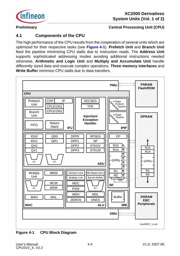
XC2000 DerivativesSystem Units (Vol. 1 of 2)
Central Processing Unit (CPU)Preliminary
4.1 Components of the CPUThe high performance of the CPU results from the cooperation of several units which areoptimized for their respective tasks (see Figure 4-1). Prefetch Unit and Branch Unitfeed the pipeline minimizing CPU stalls due to instruction reads. The Address Unitsupports sophisticated addressing modes avoiding additional instructions neededotherwise. Arithmetic and Logic Unit and Multiply and Accumulate Unit handledifferently sized data and execute complex operations. Three memory interfaces andWrite Buffer minimize CPU stalls due to data transfers.
Figure 4-1 CPU Block Diagram
DPRAM
CPU
IPIP
RFR0R1
GPRs
R14R15
R0R1
GPRs
R14R15
IFU
Injection/ExceptionHandler
ADU
MAC
mca04917_x.vsd
CPUCON1CPUCON2
CSP IP
ReturnStackFIFO
BranchUnit
PrefetchUnit
VECSEG
TFR
+/-
IDX0IDX1QX0QX1
QR0QR1
DPP0DPP1DPP2DPP3
SPSEGSP
STKOVSTKUN
+/-
MRW
MCWMSW
MAL
+/-
MAH
MultiplyUnit
ALU
Division Unit
Multiply Unit
Bit-Mask-Gen.
Barrel-Shifter
+/-MDC
PSW
MDH
ZEROS
MDL
ONES
R0R1
GPRs
R14R15
CP
WB
Buffer
2-StagePrefetch
Pipeline
5-StagePipeline
R0R1
GPRs
R14R15
PMU
DMU
DSRAMEBC
Peripherals
PSRAMFlash/ROM
User’s Manual 4-4 V1.0, 2007-06CPUSV2_X, V2.2
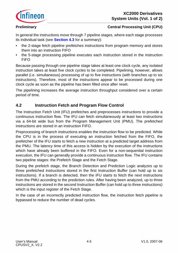
XC2000 DerivativesSystem Units (Vol. 1 of 2)
Central Processing Unit (CPU)Preliminary
In general the instructions move through 7 pipeline stages, where each stage processesits individual task (see Section 4.3 for a summary):• the 2-stage fetch pipeline prefetches instructions from program memory and stores
them into an instruction FIFO• the 5-stage processing pipeline executes each instruction stored in the instruction
FIFOBecause passing through one pipeline stage takes at least one clock cycle, any isolatedinstruction takes at least five clock cycles to be completed. Pipelining, however, allowsparallel (i.e. simultaneous) processing of up to five instructions (with branches up to sixinstructions). Therefore, most of the instructions appear to be processed during oneclock cycle as soon as the pipeline has been filled once after reset.The pipelining increases the average instruction throughput considered over a certainperiod of time.
4.2 Instruction Fetch and Program Flow ControlThe Instruction Fetch Unit (IFU) prefetches and preprocesses instructions to provide acontinuous instruction flow. The IFU can fetch simultaneously at least two instructionsvia a 64-bit wide bus from the Program Management Unit (PMU). The prefetchedinstructions are stored in an instruction FIFO.Preprocessing of branch instructions enables the instruction flow to be predicted. Whilethe CPU is in the process of executing an instruction fetched from the FIFO, theprefetcher of the IFU starts to fetch a new instruction at a predicted target address fromthe PMU. The latency time of this access is hidden by the execution of the instructionswhich have already been buffered in the FIFO. Even for a non-sequential instructionexecution, the IFU can generally provide a continuous instruction flow. The IFU containstwo pipeline stages: the Prefetch Stage and the Fetch Stage.During the prefetch stage, the Branch Detection and Prediction Logic analyzes up tothree prefetched instructions stored in the first Instruction Buffer (can hold up to sixinstructions). If a branch is detected, then the IFU starts to fetch the next instructionsfrom the PMU according to the prediction rules. After having been analyzed, up to threeinstructions are stored in the second Instruction Buffer (can hold up to three instructions)which is the input register of the Fetch Stage.In the case of an incorrectly predicted instruction flow, the instruction fetch pipeline isbypassed to reduce the number of dead cycles.
User’s Manual 4-5 V1.0, 2007-06CPUSV2_X, V2.2
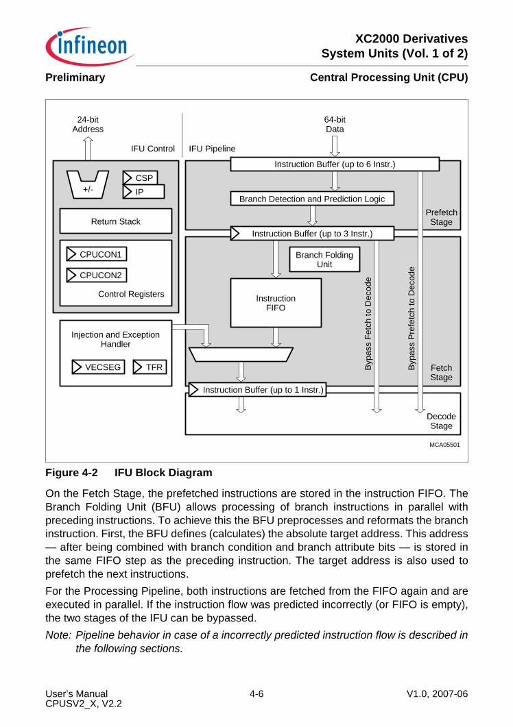
XC2000 DerivativesSystem Units (Vol. 1 of 2)
Central Processing Unit (CPU)Preliminary
Figure 4-2 IFU Block Diagram
On the Fetch Stage, the prefetched instructions are stored in the instruction FIFO. TheBranch Folding Unit (BFU) allows processing of branch instructions in parallel withpreceding instructions. To achieve this the BFU preprocesses and reformats the branchinstruction. First, the BFU defines (calculates) the absolute target address. This address— after being combined with branch condition and branch attribute bits — is stored inthe same FIFO step as the preceding instruction. The target address is also used toprefetch the next instructions.For the Processing Pipeline, both instructions are fetched from the FIFO again and areexecuted in parallel. If the instruction flow was predicted incorrectly (or FIFO is empty),the two stages of the IFU can be bypassed.Note: Pipeline behavior in case of a incorrectly predicted instruction flow is described in
the following sections.
MCA05501
Branch Detection and Prediction Logic
64-bitData
Instruction Buffer (up to 3 Instr.)
InstructionFIFO
Branch FoldingUnit
PrefetchStage
Bypa
ss F
etch
to D
ecod
e
Bypa
ss P
refe
tch
to D
ecod
e
FetchStage
DecodeStage
Instruction Buffer (up to 1 Instr.)
Injection and ExceptionHandler
TFRVECSEG
Control Registers
CPUCON2
Return Stack
CPUCON1
24-bitAddress
IFU Control IFU Pipeline
CSPIP+/-
Instruction Buffer (up to 6 Instr.)
User’s Manual 4-6 V1.0, 2007-06CPUSV2_X, V2.2
XC2000 DerivativesSystem Units (Vol. 1 of 2)
Central Processing Unit (CPU)Preliminary
4.2.1 Branch Detection and Branch Prediction RulesThe Branch Detection Unit preprocesses instructions and classifies detected branches.Depending on the branch class, the Branch Prediction Unit predicts the program flowusing the following rules:
4.2.2 Correctly Predicted Instruction FlowTable 4-2 shows the continuous execution of instructions, assuming a 0-waitstateprogram memory. In this example, most of the instructions are executed in one CPUcycle while instruction In+6 takes two CPU cycles (general example for multicycleinstructions). The diagram shows the sequential instruction flow through the differentpipeline stages. Figure 4-3 shows the corresponding program memory section.The instructions for the processing pipeline are fetched from the Instruction FIFO whilethe IFU prefetches the next instructions to fill the FIFO. As long as the instruction flow iscorrectly predicted by the IFU, both processes are independent.In this example with a fast Internal Program Memory, the Prefetcher is able to fetch moreinstructions than the processing pipeline can execute. In Tn+4, the FIFO and prefetchbuffer are filled and no further instructions can be prefetched. The PMU address stays
Table 4-1 Branch Classes and Prediction RulesBranch Instruction Classes Instructions Prediction Rule (Assumption)Inter-segment branch instructions
JMPS seg, caddrCALLS seg, caddr
The branch is always taken
Branch instructions withuser programmable branch prediction
JMPA- xcc, caddrJMPA+ xcc, caddrCALLA- xcc, caddrCALLA+ xcc, caddr
User-specified1) via bit 8 (‘a’) of the instruction long word:…+: branch ‘taken’ (a = 0)…-: branch ‘not taken’ (a = 1)
1) This bit can be also set/cleared automatically by the Assembler for generic JMPA and CALLA instructionsdepending on the jump condition (condition is cc_Z: ‘not taken’, otherwise: ‘taken’).
Indirect branch instructions JMPI cc, [Rw]CALLI cc, [Rw]
Unconditional: branch ‘taken’Conditional: ‘not taken’
Relative branch instructions with condition code
JMPR cc, rel Unconditional or backward: branch ‘taken’Conditional forward: ‘not taken’
Relative branch instructions without condition code
CALLR rel The branch is always taken
Branch instructions with bit-condition
JB(C) bitaddr, relJNB(S) bitaddr, rel
Backward: branch ‘taken’Forward: ‘not taken’
Return instructions RET, RETPRETS, RETI
The branch is always taken
User’s Manual 4-7 V1.0, 2007-06CPUSV2_X, V2.2
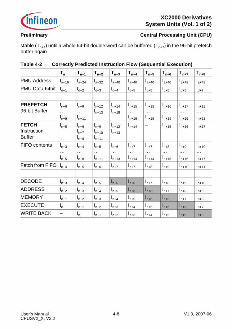
XC2000 DerivativesSystem Units (Vol. 1 of 2)
Central Processing Unit (CPU)Preliminary
stable (Tn+4) until a whole 64-bit double word can be buffered (Tn+7) in the 96-bit prefetchbuffer again.
Table 4-2 Correctly Predicted Instruction Flow (Sequential Execution)Tn Tn+1 Tn+2 Tn+3 Tn+4 Tn+5 Tn+6 Tn+7 Tn+8
PMU Address Ia+16 Ia+24 Ia+32 Ia+40 Ia+40 Ia+40 Ia+40 Ia+48 Ia+48
PMU Data 64bit Id+1 Id+2 Id+3 Id+4 Id+5 Id+5 Id+5 Id+5 Id+7
PREFETCH96-bit Buffer
In+6…In+9
In+9…In+11
In+12In+13
In+14In+15
In+15…In+19
In+15…In+19
In+16…In+19
In+17…In+19
In+18…In+21
FETCHInstruction Buffer
In+5 In+6In+7In+8
In+9In+10In+11
In+12In+13
In+14 – In+15 In+16 In+17
FIFO contents In+3…In+5
In+4…In+8
In+5…In+11
In+6…In+13
In+7…In+14
In+7…In+14
In+8…In+15
In+9…In+16
In+10…In+17
Fetch from FIFO In+4 In+5 In+6 In+7 In+7 In+8 In+9 In+10 In+11
DECODE In+3 In+4 In+5 In+6 In+6 In+7 In+8 In+9 In+10
ADDRESS In+2 In+3 In+4 In+5 In+6 In+6 In+7 In+8 In+9
MEMORY In+1 In+2 In+3 In+4 In+5 In+6 In+6 In+7 In+8
EXECUTE In In+1 In+2 In+3 In+4 In+5 In+6 In+6 In+7
WRITE BACK – In In+1 In+2 In+3 In+4 In+5 In+6 In+6
User’s Manual 4-8 V1.0, 2007-06CPUSV2_X, V2.2

XC2000 DerivativesSystem Units (Vol. 1 of 2)
Central Processing Unit (CPU)Preliminary
Figure 4-3 Program Memory Section for Correctly Predicted Flow
4.2.3 Incorrectly Predicted Instruction FlowIf the CPU detects that the IFU made an incorrect prediction of the instruction flow, thenthe pipeline stages and the Instruction FIFO containing the wrong prefetched instructionsare canceled. The entire instruction fetch is restarted at the correct point of the program.Table 4-3 shows the restarted execution of instructions, assuming a 0-waitstate programmemory. Figure 4-4 shows the corresponding program memory section.During the cycle Tn, the CPU detects an incorrectly prediction case which leads to acanceling of the pipeline. The new address is transferred to the PMU in Tn+1 whichdelivers the first data in the next cycle Tn+2. But, the target instruction crosses the 64-bitmemory boundary and a second fetch in Tn+3 is required to get the entire 32-bitinstruction. In Tn+4, the Prefetch Buffer contains two 32-bit instructions while the firstinstruction Im is directly forwarded to the Decode stage.The prefetcher is now restarted and prefetches further instructions. In Tn+5, theinstruction Im+1 is forwarded from the Fetch Instruction Buffer directly to the Decodestage as well. The Fetch row shows all instructions in the Fetch Instruction Buffer andthe instructions fetched from the Instruction FIFO. The instruction Im+3 is the firstinstruction fetched from the FIFO during Tn+6. During the same cycle, instruction Im+2 wasstill forwarded from the Fetch Instruction Buffer to the Decode stage.
MCA04918
In+21 In+21 In+20 In+20
In+19 In+18 In+17 In+16
In+16 In+15 In+15 In+14
In+14 In+13 In+12 In+12
In+11 In+11 In+10 In+10
In+9 In+8 In+7 In+6
Ia+40
Ia+32
Ia+24
Ia+16
Ia+8
Ia
User’s Manual 4-9 V1.0, 2007-06CPUSV2_X, V2.2

XC2000 DerivativesSystem Units (Vol. 1 of 2)
Central Processing Unit (CPU)Preliminary
Figure 4-4 Program Memory Section for Incorrectly Predicted Flow
Table 4-3 Incorrectly Predicted Instruction Flow (Restarted Execution)Tn Tn+1 Tn+2 Tn+3 Tn+4 Tn+5 Tn+6 Tn+7 Tn+8
PMU Address I… Ia Ia+8 Ia+16 Ia+24 I… I… I… I…PMU Data 64bit I… – Id Id+1 Id+2 Id+3 I… I… I…
PREFETCH96-bit Buffer
I… – – – ImIm+1
Im+2Im+3
Im+4Im+5
I… I…
FETCHInstruction Buffer
Inext+2 – – – – Im+1 Im+2Im+3
Im+4Im+5
I…
Fetch from FIFO – – – – – – Im+3 Im+4 Im+5
DECODE Inext+1 – – – Im Im+1 Im+2 Im+3 Im+4
ADDRESS Inext – – – – Im Im+1 Im+2 Im+3
MEMORY Ibranch – – – – – Im Im+1 Im+2
EXECUTE In Ibranch – – – – – Im Im+1
WRITE BACK – In Ibranch – – – – – Im
MCA04919
I... Im+5 Im+5 Im+4
Im+4 Im+3 Im+3
Im+1
Ia+24
Ia+16
Ia+8
Ia
I...
Im+2
ImIm+1Im+2
Im I... I...
64-bit wide Program Memory with four 16 bit packages
User’s Manual 4-10 V1.0, 2007-06CPUSV2_X, V2.2
XC2000 DerivativesSystem Units (Vol. 1 of 2)
Central Processing Unit (CPU)Preliminary
4.3 Instruction Processing PipelineThe XC2000 uses five pipeline stages to execute an instruction. All instructions passthrough each of the five stages of the instruction processing pipeline. The pipeline stagesare listed here together with the 2 stages of the fetch pipeline:1st -> PREFETCH: This stage prefetches instructions from the PMU in the predictedorder. The instructions are preprocessed in the branch detection unit to detect branches.The prediction logic decides if the branches are assumed to be taken or not.2nd -> FETCH: The instruction pointer of the next instruction to be fetched is calculatedaccording to the branch prediction rules. For zero-cycle branch execution, the BranchFolding Unit preprocesses and combines detected branches with the precedinginstructions. Prefetched instructions are stored in the instruction FIFO. At the same time,instructions are transported out of the instruction FIFO to be executed in the instructionprocessing pipeline.3rd -> DECODE: The instructions are decoded and, if required, the register file isaccessed to read the GPR used in indirect addressing modes.4th -> ADDRESS: All the operand addresses are calculated. Register SP isdecremented or incremented for all instructions which implicitly access the system stack.5th -> MEMORY: All the required operands are fetched.6th -> EXECUTE: An ALU or MAC-Unit operation is performed on the previously fetchedoperands. The condition flags are updated. All explicit write operations to CPU-SFRsand all auto-increment/auto-decrement operations of GPRs used as indirect addresspointers are performed.7th -> WRITE BACK: All external operands and the remaining operands within theinternal DPRAM space are written back. Operands located in the internal SRAM arebuffered in the Write Back Buffer.Specific so-called injected instructions are generated internally to provide the timeneeded to process instructions requiring more than one CPU cycle for processing. Theyare automatically injected into the decode stage of the pipeline, then they pass throughthe remaining stages like every standard instruction. Program interrupt, PEC transfer,and OCE operations are also performed by means of injected instructions. Althoughthese internally injected instructions will not be noticed in reality, they help to explain theoperation of the pipeline.The performance of the CPU (pipeline) is decreased by bandwidth limitations (sameresource is accessed by different stages) and data dependencies between instructions.The XC2000’s CPU has dedicated hardware to detect and to resolve different kinds ofdependencies. Some of those dependencies are described in the following section.Because up to five different instructions are processed simultaneously, additionalhardware has been dedicated to deal with dependencies which may exist betweeninstructions in different pipeline stages. This extra hardware supports ‘forwarding’ of theoperand read and write values and resolves most of the possible conflicts — such as
User’s Manual 4-11 V1.0, 2007-06CPUSV2_X, V2.2
XC2000 DerivativesSystem Units (Vol. 1 of 2)
Central Processing Unit (CPU)Preliminary
multiple usage of buses — in a time optimized way without performance loss. Thismakes the pipeline unnoticeable for the user in most cases. However, there are somerare cases in which the pipeline requires attention by the programmer. In these cases,the delays caused by the pipeline conflicts can be used for other instructions to optimizeperformance.Note: The XC2000 has a fully interlocked pipeline, which means that these conflicts do
not cause any malfunction. Instruction re-ordering is only required for performancereasons.
The following examples describe the pipeline behavior in special cases and giveprinciple rules to improve the performance by re-ordering the execution of instructions.
User’s Manual 4-12 V1.0, 2007-06CPUSV2_X, V2.2
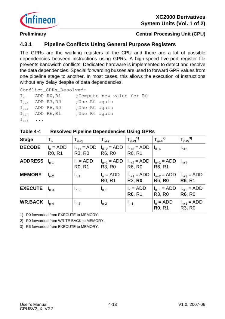
XC2000 DerivativesSystem Units (Vol. 1 of 2)
Central Processing Unit (CPU)Preliminary
4.3.1 Pipeline Conflicts Using General Purpose RegistersThe GPRs are the working registers of the CPU and there are a lot of possibledependencies between instructions using GPRs. A high-speed five-port register fileprevents bandwidth conflicts. Dedicated hardware is implemented to detect and resolvethe data dependencies. Special forwarding busses are used to forward GPR values fromone pipeline stage to another. In most cases, this allows the execution of instructionswithout any delay despite of data dependencies.Conflict_GPRs_Resolved:In ADD R0,R1 ;Compute new value for R0In+1 ADD R3,R0 ;Use R0 againIn+2 ADD R6,R0 ;Use R0 againIn+3 ADD R6,R1 ;Use R6 againIn+4 ...
Table 4-4 Resolved Pipeline Dependencies Using GPRsStage Tn Tn+1 Tn+2 Tn+3
1)
1) R0 forwarded from EXECUTE to MEMORY.
Tn+42)
2) R0 forwarded from WRITE BACK to MEMORY.
Tn+53)
3) R6 forwarded from EXECUTE to MEMORY.
DECODE In = ADD R0, R1
In+1 = ADD R3, R0
In+2 = ADD R6, R0
In+3 = ADD R6, R1
In+4 In+5
ADDRESS In-1 In = ADD R0, R1
In+1 = ADD R3, R0
In+2 = ADD R6, R0
In+3 = ADD R6, R1
In+4
MEMORY In-2 In-1 In = ADD R0, R1
In+1 = ADD R3, R0
In+2 = ADD R6, R0
In+3 = ADD R6, R1
EXECUTE In-3 In-2 In-1 In = ADD R0, R1
In+1 = ADD R3, R0
In+2 = ADD R6, R0
WR.BACK In-4 In-3 In-2 In-1 In = ADD R0, R1
In+1 = ADD R3, R0
User’s Manual 4-13 V1.0, 2007-06CPUSV2_X, V2.2
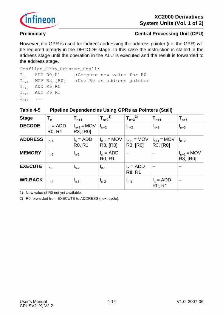
XC2000 DerivativesSystem Units (Vol. 1 of 2)
Central Processing Unit (CPU)Preliminary
However, if a GPR is used for indirect addressing the address pointer (i.e. the GPR) willbe required already in the DECODE stage. In this case the instruction is stalled in theaddress stage until the operation in the ALU is executed and the result is forwarded tothe address stage.Conflict_GPRs_Pointer_Stall:In ADD R0,R1 ;Compute new value for R0In+1 MOV R3,[R0] ;Use R0 as address pointerIn+2 ADD R6,R0In+3 ADD R6,R1In+4 ...
Table 4-5 Pipeline Dependencies Using GPRs as Pointers (Stall)Stage Tn Tn+1 Tn+2
1)
1) New value of R0 not yet available.
Tn+32)
2) R0 forwarded from EXECUTE to ADDRESS (next cycle).
Tn+4 Tn+5
DECODE In = ADD R0, R1
In+1 = MOV R3, [R0]
In+2 In+2 In+2 In+3
ADDRESS In-1 In = ADD R0, R1
In+1 = MOV R3, [R0]
In+1 = MOV R3, [R0]
In+1 = MOV R3, [R0]
In+2
MEMORY In-2 In-1 In = ADD R0, R1
– – In+1 = MOV R3, [R0]
EXECUTE In-3 In-2 In-1 In = ADD R0, R1
– –
WR.BACK In-4 In-3 In-2 In-1 In = ADD R0, R1
–
User’s Manual 4-14 V1.0, 2007-06CPUSV2_X, V2.2
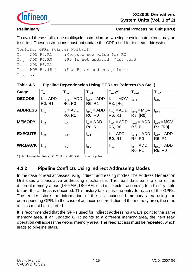
XC2000 DerivativesSystem Units (Vol. 1 of 2)
Central Processing Unit (CPU)Preliminary
To avoid these stalls, one multicycle instruction or two single cycle instructions may beinserted. These instructions must not update the GPR used for indirect addressing.Conflict_GPRs_Pointer_NoStall:In ADD R0,R1 ;Compute new value for R0In+1 ADD R6,R0 ;R0 is not updated, just readIn+2 ADD R6,R1In+3 MOV R3,[R0] ;Use R0 as address pointerIn+4 ...
4.3.2 Pipeline Conflicts Using Indirect Addressing ModesIn the case of read accesses using indirect addressing modes, the Address GenerationUnit uses a speculative addressing mechanism. The read data path to one of thedifferent memory areas (DPRAM, DSRAM, etc.) is selected according to a history tablebefore the address is decoded. This history table has one entry for each of the GPRs.The entries store the information of the last accessed memory area using thecorresponding GPR. In the case of an incorrect prediction of the memory area, the readaccess must be restarted.It is recommended that the GPRs used for indirect addressing always point to the samememory area. If an updated GPR points to a different memory area, the next readoperation will access the wrong memory area. The read access must be repeated, whichleads to pipeline stalls.
Table 4-6 Pipeline Dependencies Using GPRs as Pointers (No Stall)Stage Tn Tn+1 Tn+2 Tn+3
1)
1) R0 forwarded from EXECUTE to ADDRESS (next cycle).
Tn+4 Tn+5
DECODE In = ADD R0, R1
In+1 = ADD R6, R0
In+2 = ADD R6, R1
In+3 = MOV R3, [R0]
In+4 In+5
ADDRESS In-1 In = ADD R0, R1
In+1 = ADD R6, R0
In+2 = ADD R6, R1
In+3 = MOV R3, [R0]
In+4
MEMORY In-2 In-1 In = ADD R0, R1
In+1 = ADD R6, R0
In+2 = ADD R6, R1
In+3 = MOV R3, [R0]
EXECUTE In-3 In-2 In-1 In = ADD R0, R1
In+1 = ADD R6, R0
In+2 = ADD R6, R1
WR.BACK In-4 In-3 In-2 In-1 In = ADD R0, R1
In+1 = ADD R6, R0
User’s Manual 4-15 V1.0, 2007-06CPUSV2_X, V2.2
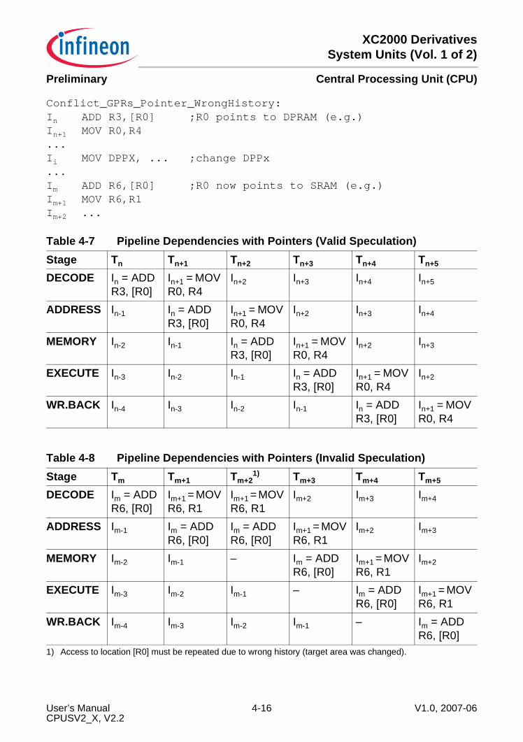
XC2000 DerivativesSystem Units (Vol. 1 of 2)
Central Processing Unit (CPU)Preliminary
Conflict_GPRs_Pointer_WrongHistory:In ADD R3,[R0] ;R0 points to DPRAM (e.g.)In+1 MOV R0,R4...Ii MOV DPPX, ... ;change DPPx...Im ADD R6,[R0] ;R0 now points to SRAM (e.g.)Im+1 MOV R6,R1Im+2 ...
Table 4-7 Pipeline Dependencies with Pointers (Valid Speculation)Stage Tn Tn+1 Tn+2 Tn+3 Tn+4 Tn+5
DECODE In = ADD R3, [R0]
In+1 = MOV R0, R4
In+2 In+3 In+4 In+5
ADDRESS In-1 In = ADD R3, [R0]
In+1 = MOV R0, R4
In+2 In+3 In+4
MEMORY In-2 In-1 In = ADD R3, [R0]
In+1 = MOV R0, R4
In+2 In+3
EXECUTE In-3 In-2 In-1 In = ADD R3, [R0]
In+1 = MOV R0, R4
In+2
WR.BACK In-4 In-3 In-2 In-1 In = ADD R3, [R0]
In+1 = MOV R0, R4
Table 4-8 Pipeline Dependencies with Pointers (Invalid Speculation)Stage Tm Tm+1 Tm+2
1)
1) Access to location [R0] must be repeated due to wrong history (target area was changed).
Tm+3 Tm+4 Tm+5
DECODE Im = ADD R6, [R0]
Im+1 = MOV R6, R1
Im+1 = MOV R6, R1
Im+2 Im+3 Im+4
ADDRESS Im-1 Im = ADD R6, [R0]
Im = ADD R6, [R0]
Im+1 = MOV R6, R1
Im+2 Im+3
MEMORY Im-2 Im-1 – Im = ADD R6, [R0]
Im+1 = MOV R6, R1
Im+2
EXECUTE Im-3 Im-2 Im-1 – Im = ADD R6, [R0]
Im+1 = MOV R6, R1
WR.BACK Im-4 Im-3 Im-2 Im-1 – Im = ADD R6, [R0]
User’s Manual 4-16 V1.0, 2007-06CPUSV2_X, V2.2
XC2000 DerivativesSystem Units (Vol. 1 of 2)
Central Processing Unit (CPU)Preliminary
4.3.3 Pipeline Conflicts Due to Memory BandwidthMemory bandwidth conflicts can occur if instructions in the pipeline access the samememory area at the same time. Special access mechanisms are implemented tominimize conflicts. The DPRAM of the CPU has two independent read/write ports; thisallows parallel read and write operation without delays. Write accesses to the DSRAMcan be buffered in a Write Back Buffer until read accesses are finished.All instructions except the CoXXX instructions can read only one memory operand percycle. A conflict between the read and one write access cannot occur because theDPRAM has two independent read/write ports. Only other pipeline stall conditions cangenerate a DPRAM bandwidth conflict. The DPRAM is a synchronous pipelinedmemory. The read access starts with the valid addresses on the address stage. The dataare delivered in the Memory stage. If a memory read access is stalled in the Memorystage and the following instruction on the Address stage tries to start a memory read, thenew read access must be delayed as well. But, this conflict is hidden by an alreadyexisting stall of the pipeline.
User’s Manual 4-17 V1.0, 2007-06CPUSV2_X, V2.2
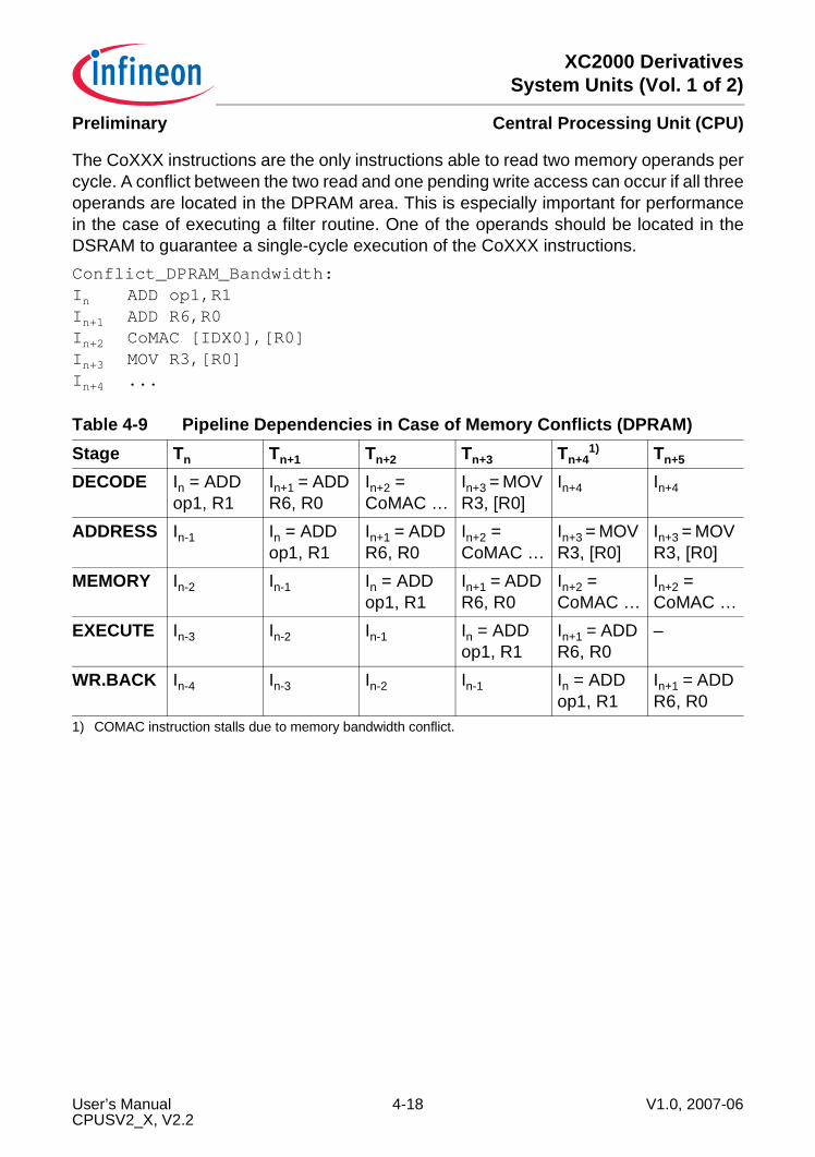
XC2000 DerivativesSystem Units (Vol. 1 of 2)
Central Processing Unit (CPU)Preliminary
The CoXXX instructions are the only instructions able to read two memory operands percycle. A conflict between the two read and one pending write access can occur if all threeoperands are located in the DPRAM area. This is especially important for performancein the case of executing a filter routine. One of the operands should be located in theDSRAM to guarantee a single-cycle execution of the CoXXX instructions.Conflict_DPRAM_Bandwidth:In ADD op1,R1In+1 ADD R6,R0In+2 CoMAC [IDX0],[R0]In+3 MOV R3,[R0]In+4 ...
Table 4-9 Pipeline Dependencies in Case of Memory Conflicts (DPRAM)Stage Tn Tn+1 Tn+2 Tn+3 Tn+4
1)
1) COMAC instruction stalls due to memory bandwidth conflict.
Tn+5
DECODE In = ADD op1, R1
In+1 = ADD R6, R0
In+2 = CoMAC …
In+3 = MOV R3, [R0]
In+4 In+4
ADDRESS In-1 In = ADD op1, R1
In+1 = ADD R6, R0
In+2 = CoMAC …
In+3 = MOV R3, [R0]
In+3 = MOV R3, [R0]
MEMORY In-2 In-1 In = ADD op1, R1
In+1 = ADD R6, R0
In+2 = CoMAC …
In+2 = CoMAC …
EXECUTE In-3 In-2 In-1 In = ADD op1, R1
In+1 = ADD R6, R0
–
WR.BACK In-4 In-3 In-2 In-1 In = ADD op1, R1
In+1 = ADD R6, R0
User’s Manual 4-18 V1.0, 2007-06CPUSV2_X, V2.2
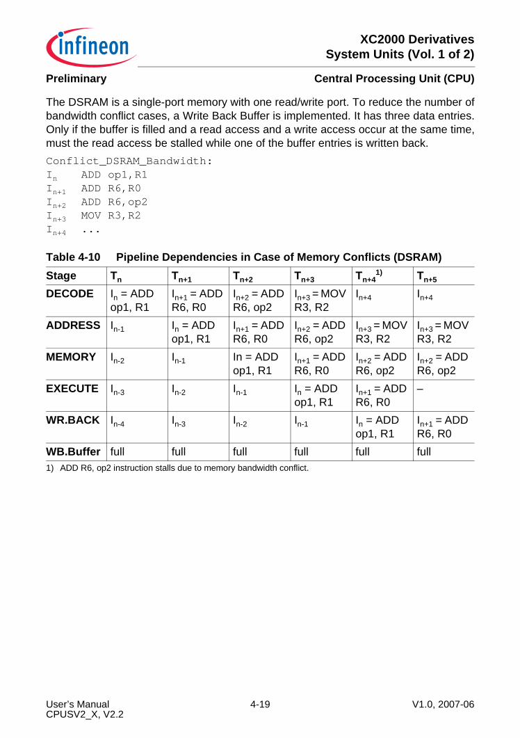
XC2000 DerivativesSystem Units (Vol. 1 of 2)
Central Processing Unit (CPU)Preliminary
The DSRAM is a single-port memory with one read/write port. To reduce the number ofbandwidth conflict cases, a Write Back Buffer is implemented. It has three data entries.Only if the buffer is filled and a read access and a write access occur at the same time,must the read access be stalled while one of the buffer entries is written back.Conflict_DSRAM_Bandwidth:In ADD op1,R1In+1 ADD R6,R0In+2 ADD R6,op2In+3 MOV R3,R2In+4 ...
Table 4-10 Pipeline Dependencies in Case of Memory Conflicts (DSRAM)Stage Tn Tn+1 Tn+2 Tn+3 Tn+4
1)
1) ADD R6, op2 instruction stalls due to memory bandwidth conflict.
Tn+5
DECODE In = ADD op1, R1
In+1 = ADD R6, R0
In+2 = ADD R6, op2
In+3 = MOV R3, R2
In+4 In+4
ADDRESS In-1 In = ADD op1, R1
In+1 = ADD R6, R0
In+2 = ADD R6, op2
In+3 = MOV R3, R2
In+3 = MOV R3, R2
MEMORY In-2 In-1 In = ADD op1, R1
In+1 = ADD R6, R0
In+2 = ADD R6, op2
In+2 = ADD R6, op2
EXECUTE In-3 In-2 In-1 In = ADD op1, R1
In+1 = ADD R6, R0
–
WR.BACK In-4 In-3 In-2 In-1 In = ADD op1, R1
In+1 = ADD R6, R0
WB.Buffer full full full full full full
User’s Manual 4-19 V1.0, 2007-06CPUSV2_X, V2.2
XC2000 DerivativesSystem Units (Vol. 1 of 2)
Central Processing Unit (CPU)Preliminary
4.3.4 Pipeline Conflicts Caused by CPU-SFR UpdatesCPU-SFRs control the CPU functionality and behavior. Changes and updates of CSFRsinfluence the instruction flow in the pipeline. Therefore, special care is required to ensurethat instructions in the pipeline always work with the correct CSFR values. CSFRs areupdated late on the EXECUTE stage of the pipeline. Meanwhile, without conflictdetection, the instructions in the DECODE, ADDRESS, and MEMORY stages would stillwork without updated register values. The CPU detects conflict cases and stalls thepipeline to guarantee a correct execution. For performance reasons, the CPUdifferentiates between different classes of CPU-SFRs. The flow of instructions throughthe pipeline can be improved by following the given rules used for instruction re-ordering.There are three classes of CPU-SFRs:• CSFRs not generating pipeline conflicts (ONES, ZEROS, MCW)• CSFR result registers updated late in the EXECUTE stage, causing one stall cycle• CSFRs affecting the whole CPU or the pipeline, causing canceling
CSFR Result RegistersThe CSFR result registers MDH, MDL, MSW, MAH, MAL, and MRW of the ALU andMAC-Unit are updated late in the EXECUTE stage of the pipeline. If an instruction(except CoSTORE) accesses explicitly these registers in the memory stage, the valuecannot be forwarded. The instruction must be stalled for one cycle on the MEMORYstage.
User’s Manual 4-20 V1.0, 2007-06CPUSV2_X, V2.2
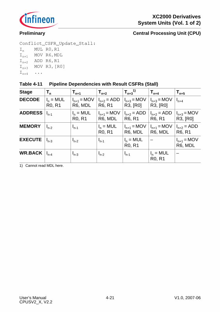
XC2000 DerivativesSystem Units (Vol. 1 of 2)
Central Processing Unit (CPU)Preliminary
Conflict_CSFR_Update_Stall:In MUL R0,R1In+1 MOV R6,MDLIn+2 ADD R6,R1In+3 MOV R3,[R0]In+4 ...
Table 4-11 Pipeline Dependencies with Result CSFRs (Stall)Stage Tn Tn+1 Tn+2 Tn+3
1)
1) Cannot read MDL here.
Tn+4 Tn+5
DECODE In = MUL R0, R1
In+1 = MOV R6, MDL
In+2 = ADD R6, R1
In+3 = MOV R3, [R0]
In+3 = MOV R3, [R0]
In+4
ADDRESS In-1 In = MUL R0, R1
In+1 = MOV R6, MDL
In+2 = ADD R6, R1
In+2 = ADD R6, R1
In+3 = MOV R3, [R0]
MEMORY In-2 In-1 In = MUL R0, R1
In+1 = MOV R6, MDL
In+1 = MOV R6, MDL
In+2 = ADD R6, R1
EXECUTE In-3 In-2 In-1 In = MUL R0, R1
– In+1 = MOV R6, MDL
WR.BACK In-4 In-3 In-2 In-1 In = MUL R0, R1
–
User’s Manual 4-21 V1.0, 2007-06CPUSV2_X, V2.2
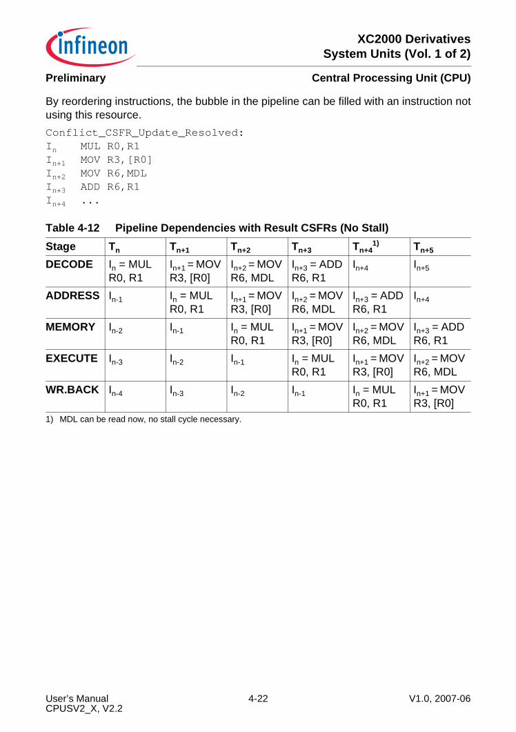
XC2000 DerivativesSystem Units (Vol. 1 of 2)
Central Processing Unit (CPU)Preliminary
By reordering instructions, the bubble in the pipeline can be filled with an instruction notusing this resource.Conflict_CSFR_Update_Resolved:In MUL R0,R1In+1 MOV R3,[R0]In+2 MOV R6,MDLIn+3 ADD R6,R1In+4 ...
Table 4-12 Pipeline Dependencies with Result CSFRs (No Stall)Stage Tn Tn+1 Tn+2 Tn+3 Tn+4
1)
1) MDL can be read now, no stall cycle necessary.
Tn+5
DECODE In = MUL R0, R1
In+1 = MOV R3, [R0]
In+2 = MOV R6, MDL
In+3 = ADD R6, R1
In+4 In+5
ADDRESS In-1 In = MUL R0, R1
In+1 = MOV R3, [R0]
In+2 = MOV R6, MDL
In+3 = ADD R6, R1
In+4
MEMORY In-2 In-1 In = MUL R0, R1
In+1 = MOV R3, [R0]
In+2 = MOV R6, MDL
In+3 = ADD R6, R1
EXECUTE In-3 In-2 In-1 In = MUL R0, R1
In+1 = MOV R3, [R0]
In+2 = MOV R6, MDL
WR.BACK In-4 In-3 In-2 In-1 In = MUL R0, R1
In+1 = MOV R3, [R0]
User’s Manual 4-22 V1.0, 2007-06CPUSV2_X, V2.2
XC2000 DerivativesSystem Units (Vol. 1 of 2)
Central Processing Unit (CPU)Preliminary
CSFRs Affecting the Whole CPUSome CSFRs affect the whole CPU or the pipeline before the Memory stage. The CPU-SFRs CPUCON1, CP, SP, STKUN, STKOV, VECSEG, TFR, and PSW affect the overallCPU function, while the CPU-SFRs IDX0, IDX1, QX1, QX0, DPP0, DPP1, DPP2, andDPP3 only affect the DECODE, ADDRESS, and MEMORY stage when they aremodified explicitly. In this case the pipeline behavior depends on the instruction andaddressing mode used to modify the CSFR.In the case of modification of these CSFRs by “POP CSFR” or by instructions using thereg,#data16 addressing mode, a special mechanism is implemented to improveperformance during the initialization.For further explanation, the instruction which modifies the CSFR can be called“instruction_modify_CSFR”. This special case is detected in the DECODE stage whenthe instruction_modify_CSFR enters the processing pipeline. Further on, instructionsdescribed in the following list are held in the DECODE stage (all other instructions arenot held):• Instructions using long addressing mode (mem)• Instructions using indirect addressing modes ([Rw], [Rw+]…), except JMPI and CALLI• ENWDT, DISWDT, EINIT• All CoXXX instructionsIf the CPUCON1, CP, SP, STKUN, STKOV, VECSEG, TFR, or the PSW are modifiedand the instruction_modify_CSFR reaches the EXECUTE stage, the pipeline iscanceled. The modification affects the entire pipeline and the instruction prefetch. Aclean cancel and restart mechanism is required to guarantee a correct instruction flow.In case of modification of IDX0, IDX1, QX1, QX0, DPP0, DPP1, DPP2, or DPP3 only theDECODE, ADDRESS, and MEMORY stages are affected and the pipeline needs not tobe canceled. The modification does not affect the instructions in the ADDRESS,MEMORY stage because they are not using this resource. Other kinds of instructions areheld in the DECODE stage until the CSFR is modified.The following example shows a case in which the pipeline is stalled. The instruction“MOV R6, R1” after the “MOV IDX1, #12” instruction which modifies the CSFR will beheld in DECODE Stage until the IDX1 register is updated. The next example shows anoptimized initialization routine.
User’s Manual 4-23 V1.0, 2007-06CPUSV2_X, V2.2
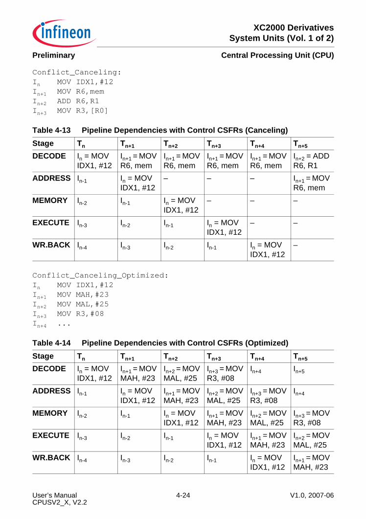
XC2000 DerivativesSystem Units (Vol. 1 of 2)
Central Processing Unit (CPU)Preliminary
Conflict_Canceling:In MOV IDX1,#12In+1 MOV R6,memIn+2 ADD R6,R1In+3 MOV R3,[R0]
Conflict_Canceling_Optimized:In MOV IDX1,#12In+1 MOV MAH,#23In+2 MOV MAL,#25In+3 MOV R3,#08In+4 ...
Table 4-13 Pipeline Dependencies with Control CSFRs (Canceling)Stage Tn Tn+1 Tn+2 Tn+3 Tn+4 Tn+5
DECODE In = MOV IDX1, #12
In+1 = MOV R6, mem
In+1 = MOV R6, mem
In+1 = MOV R6, mem
In+1 = MOV R6, mem
In+2 = ADD R6, R1
ADDRESS In-1 In = MOV IDX1, #12
– – – In+1 = MOV R6, mem
MEMORY In-2 In-1 In = MOV IDX1, #12
– – –
EXECUTE In-3 In-2 In-1 In = MOV IDX1, #12
– –
WR.BACK In-4 In-3 In-2 In-1 In = MOV IDX1, #12
–
Table 4-14 Pipeline Dependencies with Control CSFRs (Optimized)Stage Tn Tn+1 Tn+2 Tn+3 Tn+4 Tn+5
DECODE In = MOV IDX1, #12
In+1 = MOV MAH, #23
In+2 = MOV MAL, #25
In+3 = MOV R3, #08
In+4 In+5
ADDRESS In-1 In = MOV IDX1, #12
In+1 = MOV MAH, #23
In+2 = MOV MAL, #25
In+3 = MOV R3, #08
In+4
MEMORY In-2 In-1 In = MOV IDX1, #12
In+1 = MOV MAH, #23
In+2 = MOV MAL, #25
In+3 = MOV R3, #08
EXECUTE In-3 In-2 In-1 In = MOV IDX1, #12
In+1 = MOV MAH, #23
In+2 = MOV MAL, #25
WR.BACK In-4 In-3 In-2 In-1 In = MOV IDX1, #12
In+1 = MOV MAH, #23
User’s Manual 4-24 V1.0, 2007-06CPUSV2_X, V2.2

XC2000 DerivativesSystem Units (Vol. 1 of 2)
Central Processing Unit (CPU)Preliminary
For all the other instructions that modify this kind of CSFR, a simple stall and cancelmechanism guarantees the correct instruction flow.A possible explicit write-operation to this kind of CSFRs is detected on the MEMORYstage of the pipeline. The following instructions on the ADDRESS and DECODE Stageare stalled. If the instruction reaches the EXECUTE stage, the entire pipeline and theInstruction FIFO of the IFU are canceled. The instruction flow is completely re-started.Conflict_Canceling_Completely:In MOV PSW,R4In+1 MOV R6,R1In+2 ADD R6,R1In+3 MOV R3,[R0]In+4 ...
Table 4-15 Pipeline Dependencies with Control CSFRs (Cancel All)Stage Tn+1 Tn+2 Tn+3 Tn+4 Tn+5 Tn+6
DECODE In+1 = MOV R6, R1
In+2 = ADD R6, R1
In+2 = ADD R6, R1
– – In+1 = MOV R6, R1
ADDRESS In = MOV PSW, R4
In+1 = MOV R6, R1
In+1 = MOV R6, R1
– – –
MEMORY In-1 In = MOV PSW, R4
– – – –
EXECUTE In-2 In-1 In = MOV PSW, R4
– – –
WR.BACK In-3 In-2 In-1 In = MOV PSW, R4
– –
User’s Manual 4-25 V1.0, 2007-06CPUSV2_X, V2.2
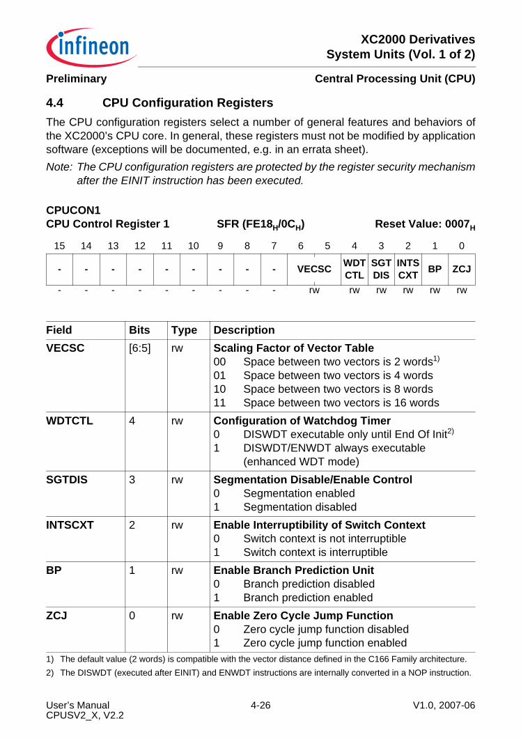
XC2000 DerivativesSystem Units (Vol. 1 of 2)
Central Processing Unit (CPU)Preliminary
4.4 CPU Configuration Registers The CPU configuration registers select a number of general features and behaviors ofthe XC2000’s CPU core. In general, these registers must not be modified by applicationsoftware (exceptions will be documented, e.g. in an errata sheet).Note: The CPU configuration registers are protected by the register security mechanism
after the EINIT instruction has been executed.
CPUCON1 CPU Control Register 1 SFR (FE18H/0CH) Reset Value: 0007H
15 14 13 12 11 10 9 8 7 6 5 4 3 2 1 0
- - - - - - - - - VECSC WDTCTL
SGTDIS
INTSCXT BP ZCJ
- - - - - - - - - rw rw rw rw rw rw
Field Bits Type DescriptionVECSC [6:5] rw Scaling Factor of Vector Table
00 Space between two vectors is 2 words1)
01 Space between two vectors is 4 words10 Space between two vectors is 8 words11 Space between two vectors is 16 words
1) The default value (2 words) is compatible with the vector distance defined in the C166 Family architecture.
WDTCTL 4 rw Configuration of Watchdog Timer0 DISWDT executable only until End Of Init2)
1 DISWDT/ENWDT always executable (enhanced WDT mode)
2) The DISWDT (executed after EINIT) and ENWDT instructions are internally converted in a NOP instruction.
SGTDIS 3 rw Segmentation Disable/Enable Control0 Segmentation enabled1 Segmentation disabled
INTSCXT 2 rw Enable Interruptibility of Switch Context0 Switch context is not interruptible1 Switch context is interruptible
BP 1 rw Enable Branch Prediction Unit0 Branch prediction disabled1 Branch prediction enabled
ZCJ 0 rw Enable Zero Cycle Jump Function0 Zero cycle jump function disabled1 Zero cycle jump function enabled
User’s Manual 4-26 V1.0, 2007-06CPUSV2_X, V2.2
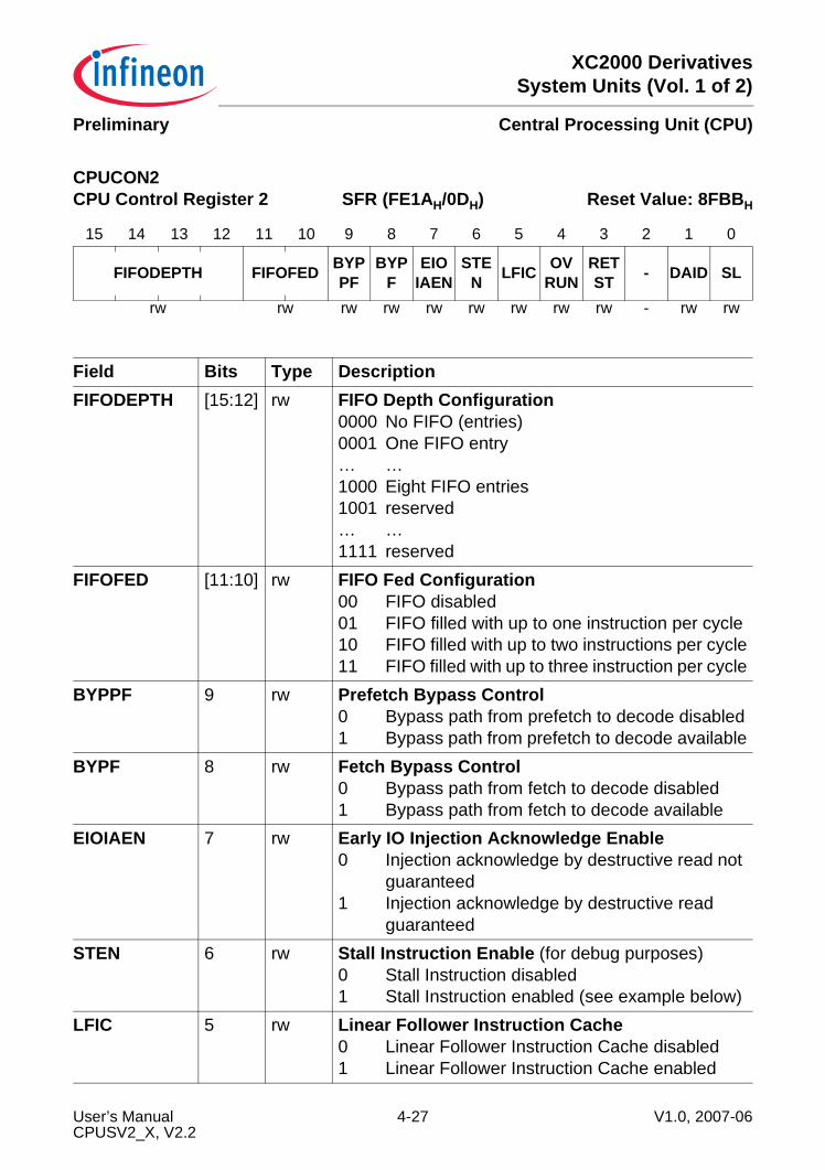
XC2000 DerivativesSystem Units (Vol. 1 of 2)
Central Processing Unit (CPU)Preliminary
CPUCON2 CPU Control Register 2 SFR (FE1AH/0DH) Reset Value: 8FBBH
15 14 13 12 11 10 9 8 7 6 5 4 3 2 1 0
FIFODEPTH FIFOFED BYPPF
BYPF
EIOIAEN
STEN LFIC OV
RUNRETST - DAID SL
rw rw rw rw rw rw rw rw rw - rw rw
Field Bits Type DescriptionFIFODEPTH [15:12] rw FIFO Depth Configuration
0000 No FIFO (entries)0001 One FIFO entry… …1000 Eight FIFO entries1001 reserved… …1111 reserved
FIFOFED [11:10] rw FIFO Fed Configuration00 FIFO disabled01 FIFO filled with up to one instruction per cycle10 FIFO filled with up to two instructions per cycle11 FIFO filled with up to three instruction per cycle
BYPPF 9 rw Prefetch Bypass Control0 Bypass path from prefetch to decode disabled1 Bypass path from prefetch to decode available
BYPF 8 rw Fetch Bypass Control0 Bypass path from fetch to decode disabled1 Bypass path from fetch to decode available
EIOIAEN 7 rw Early IO Injection Acknowledge Enable0 Injection acknowledge by destructive read not
guaranteed1 Injection acknowledge by destructive read
guaranteedSTEN 6 rw Stall Instruction Enable (for debug purposes)
0 Stall Instruction disabled1 Stall Instruction enabled (see example below)
LFIC 5 rw Linear Follower Instruction Cache0 Linear Follower Instruction Cache disabled1 Linear Follower Instruction Cache enabled
User’s Manual 4-27 V1.0, 2007-06CPUSV2_X, V2.2
XC2000 DerivativesSystem Units (Vol. 1 of 2)
Central Processing Unit (CPU)Preliminary
Example for dedicated stall debug instructions:STALLAM da,ha,dm,hm ;Opcode: 44 dahadmhmSTALLEW de,he,dw,hw ;Opcode: 45 dehedwhw ;Stalls the corresponding pipeline ;stage after “d” cycles for “h” cycles ;(“d” and “h” are 6-bit values)
Note: In general, these registers must not be modified by application software(exceptions will be documented, e.g. in an errata sheet).
OVRUN 4 rw Pipeline Control0 Overrun of pipeline bubbles not allowed1 Overrun of pipeline bubbles allowed
RETST 3 rw Enable Return Stack0 Return Stack is disabled1 Return Stack is enabled
DAID 1 rw Disable Atomic Injection Deny0 Injection-requests are denied during Atomic1 Injection-requests are not denied during
AtomicSL 0 rw Enables Short Loop Mode
0 Short loop mode disabled1 Short loop mode enabled
Field Bits Type Description
User’s Manual 4-28 V1.0, 2007-06CPUSV2_X, V2.2
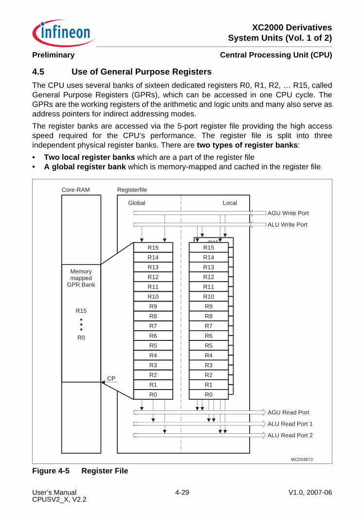
XC2000 DerivativesSystem Units (Vol. 1 of 2)
Central Processing Unit (CPU)Preliminary
4.5 Use of General Purpose RegistersThe CPU uses several banks of sixteen dedicated registers R0, R1, R2, … R15, calledGeneral Purpose Registers (GPRs), which can be accessed in one CPU cycle. TheGPRs are the working registers of the arithmetic and logic units and many also serve asaddress pointers for indirect addressing modes.The register banks are accessed via the 5-port register file providing the high accessspeed required for the CPU’s performance. The register file is split into threeindependent physical register banks. There are two types of register banks:• Two local register banks which are a part of the register file• A global register bank which is memory-mapped and cached in the register file
Figure 4-5 Register File
R15
MCD04873
R15
R14
R13
R12
R11
R10
R9
R8
R7
R6
R5
R4
R3
R2
R1
R0
R15
R14
R13
R12
R11
R10
R9
R8
R7
R6
R5
R4
R3
R2
R1
R0
Core-RAM
Global Local
R15
R0
Memorymapped
GPR Bank
AGU Write Port
ALU Write Port
AGU Read Port
ALU Read Port 1
ALU Read Port 2
Registerfile
CP
User’s Manual 4-29 V1.0, 2007-06CPUSV2_X, V2.2
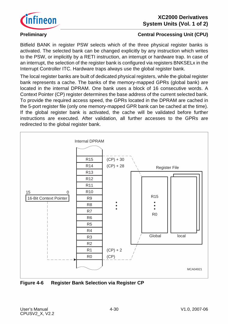
XC2000 DerivativesSystem Units (Vol. 1 of 2)
Central Processing Unit (CPU)Preliminary
Bitfield BANK in register PSW selects which of the three physical register banks isactivated. The selected bank can be changed explicitly by any instruction which writesto the PSW, or implicitly by a RETI instruction, an interrupt or hardware trap. In case ofan interrupt, the selection of the register bank is configured via registers BNKSELx in theInterrupt Controller ITC. Hardware traps always use the global register bank.The local register banks are built of dedicated physical registers, while the global registerbank represents a cache. The banks of the memory-mapped GPRs (global bank) arelocated in the internal DPRAM. One bank uses a block of 16 consecutive words. AContext Pointer (CP) register determines the base address of the current selected bank.To provide the required access speed, the GPRs located in the DPRAM are cached inthe 5-port register file (only one memory-mapped GPR bank can be cached at the time).If the global register bank is activated, the cache will be validated before furtherinstructions are executed. After validation, all further accesses to the GPRs areredirected to the global register bank.
Figure 4-6 Register Bank Selection via Register CP
MCA04921
R15
R13
R12
R11
R10
R9
R8
R7
R6
R5
R4
R3
R2
R1
R0
16-Bit Context Pointer
15 0
Internal DPRAM
R15
R0
Global local
Register File
(CP) + 30
R14 (CP) + 28
(CP) + 2
(CP)
User’s Manual 4-30 V1.0, 2007-06CPUSV2_X, V2.2
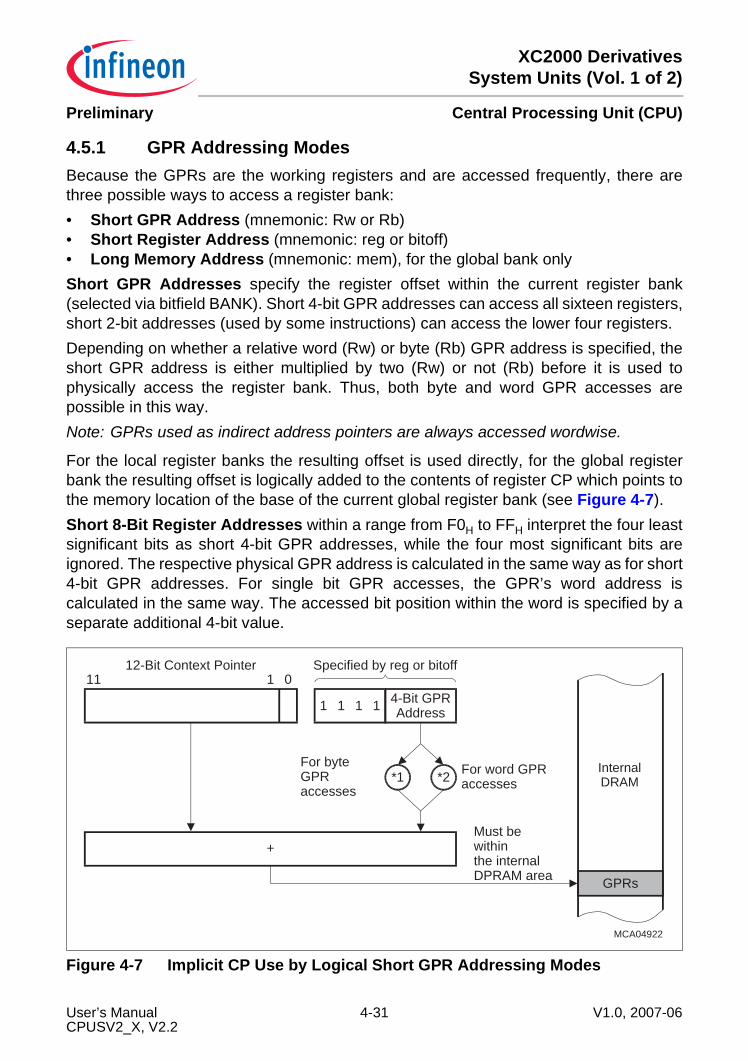
XC2000 DerivativesSystem Units (Vol. 1 of 2)
Central Processing Unit (CPU)Preliminary
4.5.1 GPR Addressing ModesBecause the GPRs are the working registers and are accessed frequently, there arethree possible ways to access a register bank:• Short GPR Address (mnemonic: Rw or Rb)• Short Register Address (mnemonic: reg or bitoff)• Long Memory Address (mnemonic: mem), for the global bank onlyShort GPR Addresses specify the register offset within the current register bank(selected via bitfield BANK). Short 4-bit GPR addresses can access all sixteen registers,short 2-bit addresses (used by some instructions) can access the lower four registers.Depending on whether a relative word (Rw) or byte (Rb) GPR address is specified, theshort GPR address is either multiplied by two (Rw) or not (Rb) before it is used tophysically access the register bank. Thus, both byte and word GPR accesses arepossible in this way.Note: GPRs used as indirect address pointers are always accessed wordwise.
For the local register banks the resulting offset is used directly, for the global registerbank the resulting offset is logically added to the contents of register CP which points tothe memory location of the base of the current global register bank (see Figure 4-7).Short 8-Bit Register Addresses within a range from F0H to FFH interpret the four leastsignificant bits as short 4-bit GPR addresses, while the four most significant bits areignored. The respective physical GPR address is calculated in the same way as for short4-bit GPR addresses. For single bit GPR accesses, the GPR’s word address iscalculated in the same way. The accessed bit position within the word is specified by aseparate additional 4-bit value.
Figure 4-7 Implicit CP Use by Logical Short GPR Addressing Modes
1 4-Bit GPRAddress
MCA04922
011 1
1 1 1
12-Bit Context Pointer Specified by reg or bitoff
*1 *2
+
For word GPRaccesses
For byteGPRaccesses
GPRs
Must bewithinthe internalDPRAM area
InternalDRAM
User’s Manual 4-31 V1.0, 2007-06CPUSV2_X, V2.2
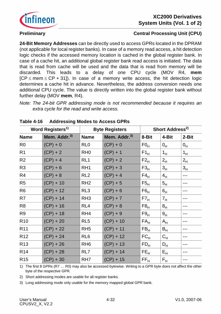
XC2000 DerivativesSystem Units (Vol. 1 of 2)
Central Processing Unit (CPU)Preliminary
24-Bit Memory Addresses can be directly used to access GPRs located in the DPRAM(not applicable for local register banks). In case of a memory read access, a hit detectionlogic checks if the accessed memory location is cached in the global register bank. Incase of a cache hit, an additional global register bank read access is initiated. The datathat is read from cache will be used and the data that is read from memory will bediscarded. This leads to a delay of one CPU cycle (MOV R4, mem[CP ≤ mem ≤ CP + 31]). In case of a memory write access, the hit detection logicdetermines a cache hit in advance. Nevertheless, the address conversion needs oneadditional CPU cycle. The value is directly written into the global register bank withoutfurther delay (MOV mem, R4).Note: The 24-bit GPR addressing mode is not recommended because it requires an
extra cycle for the read and write access.
Table 4-16 Addressing Modes to Access GPRsWord Registers1)
1) The first 8 GPRs (R7 … R0) may also be accessed bytewise. Writing to a GPR byte does not affect the otherbyte of the respective GPR.
Byte Registers Short Address2)
2) Short addressing modes are usable for all register banks.
Name Mem. Addr.3)
3) Long addressing mode only usable for the memory mapped global GPR bank.
Name Mem. Addr.3) 8-Bit 4-Bit 2-BitR0 (CP) + 0 RL0 (CP) + 0 F0H 0H 0H
R1 (CP) + 2 RH0 (CP) + 1 F1H 1H 1H
R2 (CP) + 4 RL1 (CP) + 2 F2H 2H 2H
R3 (CP) + 6 RH1 (CP) + 3 F3H 3H 3H
R4 (CP) + 8 RL2 (CP) + 4 F4H 4H ---R5 (CP) + 10 RH2 (CP) + 5 F5H 5H ---R6 (CP) + 12 RL3 (CP) + 6 F6H 6H ---R7 (CP) + 14 RH3 (CP) + 7 F7H 7H ---R8 (CP) + 16 RL4 (CP) + 8 F8H 8H ---R9 (CP) + 18 RH4 (CP) + 9 F9H 9H ---R10 (CP) + 20 RL5 (CP) + 10 FAH AH ---R11 (CP) + 22 RH5 (CP) + 11 FBH BH ---R12 (CP) + 24 RL6 (CP) + 12 FCH CH ---R13 (CP) + 26 RH6 (CP) + 13 FDH DH ---R14 (CP) + 28 RL7 (CP) + 14 FEH EH ---R15 (CP) + 30 RH7 (CP) + 15 FFH FH ---
User’s Manual 4-32 V1.0, 2007-06CPUSV2_X, V2.2
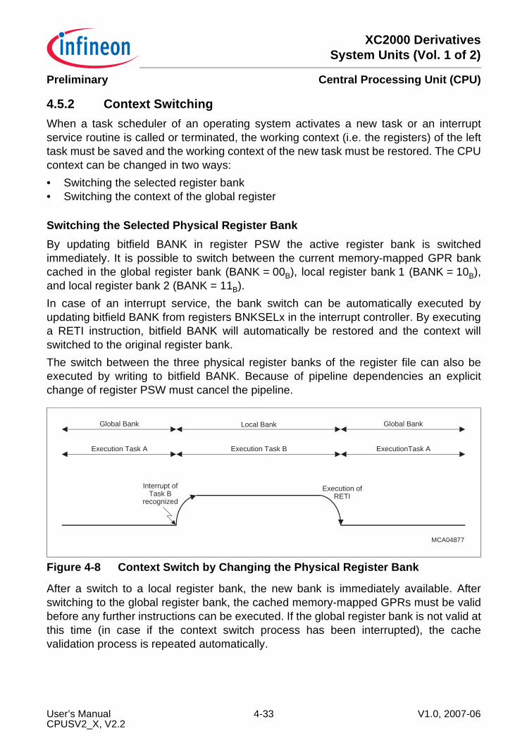
XC2000 DerivativesSystem Units (Vol. 1 of 2)
Central Processing Unit (CPU)Preliminary
4.5.2 Context SwitchingWhen a task scheduler of an operating system activates a new task or an interruptservice routine is called or terminated, the working context (i.e. the registers) of the lefttask must be saved and the working context of the new task must be restored. The CPUcontext can be changed in two ways:• Switching the selected register bank• Switching the context of the global register
Switching the Selected Physical Register BankBy updating bitfield BANK in register PSW the active register bank is switchedimmediately. It is possible to switch between the current memory-mapped GPR bankcached in the global register bank (BANK = 00B), local register bank 1 (BANK = 10B),and local register bank 2 (BANK = 11B).In case of an interrupt service, the bank switch can be automatically executed byupdating bitfield BANK from registers BNKSELx in the interrupt controller. By executinga RETI instruction, bitfield BANK will automatically be restored and the context willswitched to the original register bank.The switch between the three physical register banks of the register file can also beexecuted by writing to bitfield BANK. Because of pipeline dependencies an explicitchange of register PSW must cancel the pipeline.
Figure 4-8 Context Switch by Changing the Physical Register Bank
After a switch to a local register bank, the new bank is immediately available. Afterswitching to the global register bank, the cached memory-mapped GPRs must be validbefore any further instructions can be executed. If the global register bank is not valid atthis time (in case if the context switch process has been interrupted), the cachevalidation process is repeated automatically.
MCA04877
Interrupt ofTask B
recognized
Execution ofRETI
Execution Task A Execution Task B ExecutionTask A
Global BankLocal BankGlobal Bank
User’s Manual 4-33 V1.0, 2007-06CPUSV2_X, V2.2
XC2000 DerivativesSystem Units (Vol. 1 of 2)
Central Processing Unit (CPU)Preliminary
Switching the Context of the Global Register BankThe contents of the global register bank are switched by changing the base address ofthe memory-mapped GPR bank. The base address is given by the contents of theContext Pointer (CP).After the CP has been updated, a state machine starts to store the old contents of theglobal register bank and to load the new one. The store and load algorithm is executedin nineteen CPU cycles: the execution of the cache validation process takes sixteencycles plus three cycles to stall an instruction execution to avoid pipeline conflicts uponthe completion of the validation process. The context switch process has two phases:• Store phase: The contents of the global register bank1) is stored back into the
DPRAM by executing eight injected STORE instructions. After the last STOREinstruction the contents of the global register bank are invalidated.
• Load phase: The global register bank is loaded with the new context by executingeight injected LOAD instructions. After the last LOAD instruction the contents of theglobal register bank are validated.
The code execution is stopped until the global register bank is valid again. A hardwareinterrupt can occur during the validation process. The way the validation process iscompleted depends on the type of register bank selected for this interrupt:• If the interrupt also uses a global register bank the validation process is finished
before executing the service routine (see Figure 4-9).• If the interrupt uses a local register bank the validation process is interrupted and the
service routine is executed immediately (see Figure 4-10). After switching back tothe global register bank, the validation process is finished:– If the interrupt occurred during the store phase, the entire validation process is
restarted from the very beginning.– If the interrupt occurred during the load phase, only the load phase is repeated.
If a local-bank interrupt routine (Task B in Figure 4-11) is again interrupted by a global-bank interrupt (Task C), the suspended validation process must be finished before codeof Task C can be executed. This means that the validation process of Task A does notaffect the interrupt latency of Task B but the latency of Task C.Note: If Task C would immediately interrupt Task A, the register bank validation process
of Task A would be finished first. The worst case interrupt latency is identical inboth cases (see Figure 4-9 and Figure 4-11).
1) During the store phase of the context switch the complete register bank is written to the DPRAM even if theapplication only uses a part of this register bank. A register bank must not be located above FDE0H, otherwisethe store phase will overwrite SFRs (beginning at FE00H).
User’s Manual 4-34 V1.0, 2007-06CPUSV2_X, V2.2
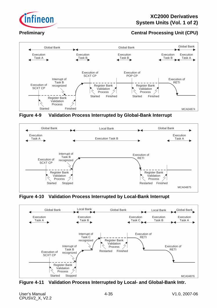
XC2000 DerivativesSystem Units (Vol. 1 of 2)
Central Processing Unit (CPU)Preliminary
Figure 4-9 Validation Process Interrupted by Global-Bank Interrupt
Figure 4-10 Validation Process Interrupted by Local-Bank Interrupt
Figure 4-11 Validation Process Interrupted by Local- and Global-Bank Intr.
MCA04874Finished
Register BankValidationProcess
Started
Execution ofSCXT CP
Interrupt ofTask B
recognized
Finished
Register BankValidationProcess
Started
Execution ofRETI
ExecutionTask A
ExecutionTask B
ExecutionTask B
ExecutionTask B
ExecutionTask A
Global BankGlobal BankGlobal Bank
Finished
Register BankValidationProcess
Started
Execution ofSCXT CP
Execution ofPOP CP
MCA04875
Stopped
Register BankValidationProcess
Started
Execution ofSCXT CP
Interrupt ofTask B
recognized
Execution ofRETI
ExecutionTask A Execution Task B
ExecutionTask A
Global BankLocal BankGlobal Bank
Finished
Register BankValidationProcess
Restarted
MCA04876Stopped
Register BankValidationProcess
Started
Execution ofSCXT CP
Interrupt ofTask B
recognized
Interrupt ofTask C
recognized
Finished
Register BankValidationProcess
Restarted
Execution ofRETI
Execution ofRETI
ExecutionTask A
ExecutionTask B
ExecutionTask C
ExecutionTask B
ExecutionTask A
Global BankLocal BankGlobal BankLocal BankGlobal Bank
User’s Manual 4-35 V1.0, 2007-06CPUSV2_X, V2.2
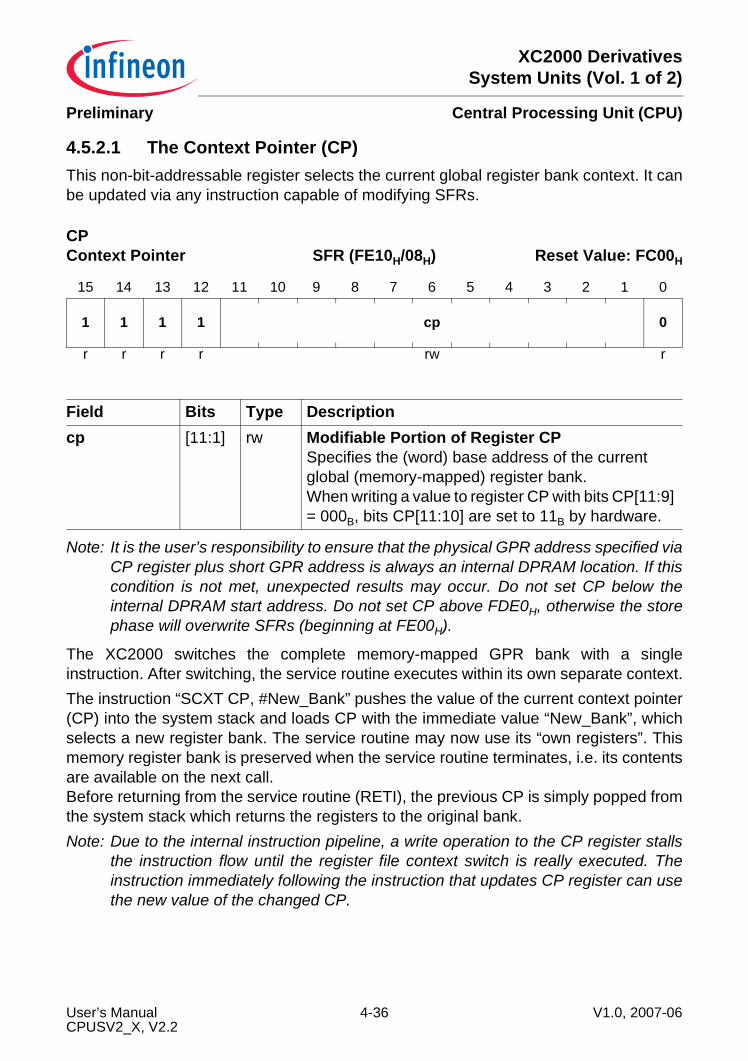
XC2000 DerivativesSystem Units (Vol. 1 of 2)
Central Processing Unit (CPU)Preliminary
4.5.2.1 The Context Pointer (CP)This non-bit-addressable register selects the current global register bank context. It canbe updated via any instruction capable of modifying SFRs.
Note: It is the user’s responsibility to ensure that the physical GPR address specified viaCP register plus short GPR address is always an internal DPRAM location. If thiscondition is not met, unexpected results may occur. Do not set CP below theinternal DPRAM start address. Do not set CP above FDE0H, otherwise the storephase will overwrite SFRs (beginning at FE00H).
The XC2000 switches the complete memory-mapped GPR bank with a singleinstruction. After switching, the service routine executes within its own separate context.The instruction “SCXT CP, #New_Bank” pushes the value of the current context pointer(CP) into the system stack and loads CP with the immediate value “New_Bank”, whichselects a new register bank. The service routine may now use its “own registers”. Thismemory register bank is preserved when the service routine terminates, i.e. its contentsare available on the next call.Before returning from the service routine (RETI), the previous CP is simply popped fromthe system stack which returns the registers to the original bank.Note: Due to the internal instruction pipeline, a write operation to the CP register stalls
the instruction flow until the register file context switch is really executed. Theinstruction immediately following the instruction that updates CP register can usethe new value of the changed CP.
CP Context Pointer SFR (FE10H/08H) Reset Value: FC00H
15 14 13 12 11 10 9 8 7 6 5 4 3 2 1 0
1 1 1 1 cp 0
r r r r rw r
Field Bits Type Descriptioncp [11:1] rw Modifiable Portion of Register CP
Specifies the (word) base address of the current global (memory-mapped) register bank.When writing a value to register CP with bits CP[11:9] = 000B, bits CP[11:10] are set to 11B by hardware.
User’s Manual 4-36 V1.0, 2007-06CPUSV2_X, V2.2
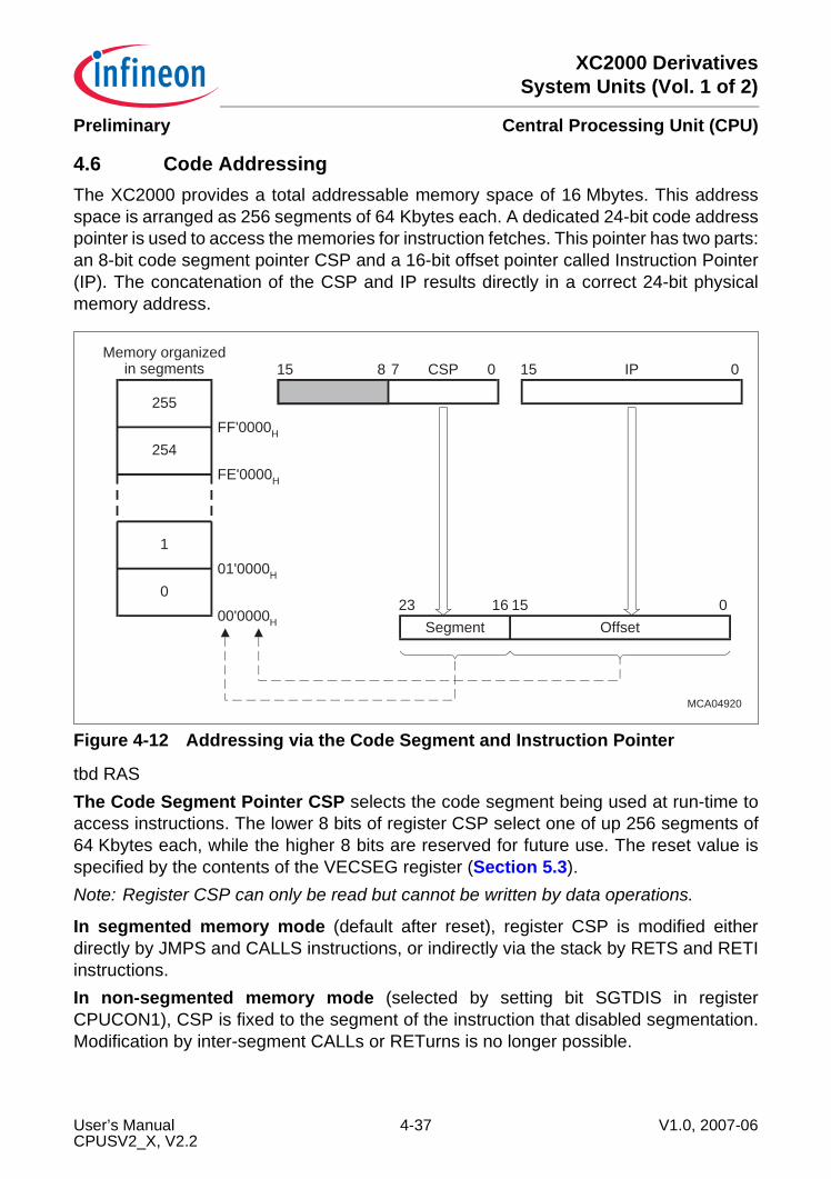
XC2000 DerivativesSystem Units (Vol. 1 of 2)
Central Processing Unit (CPU)Preliminary
4.6 Code AddressingThe XC2000 provides a total addressable memory space of 16 Mbytes. This addressspace is arranged as 256 segments of 64 Kbytes each. A dedicated 24-bit code addresspointer is used to access the memories for instruction fetches. This pointer has two parts:an 8-bit code segment pointer CSP and a 16-bit offset pointer called Instruction Pointer(IP). The concatenation of the CSP and IP results directly in a correct 24-bit physicalmemory address.
Figure 4-12 Addressing via the Code Segment and Instruction Pointer
tbd RASThe Code Segment Pointer CSP selects the code segment being used at run-time toaccess instructions. The lower 8 bits of register CSP select one of up 256 segments of64 Kbytes each, while the higher 8 bits are reserved for future use. The reset value isspecified by the contents of the VECSEG register (Section 5.3).Note: Register CSP can only be read but cannot be written by data operations.
In segmented memory mode (default after reset), register CSP is modified eitherdirectly by JMPS and CALLS instructions, or indirectly via the stack by RETS and RETIinstructions.In non-segmented memory mode (selected by setting bit SGTDIS in registerCPUCON1), CSP is fixed to the segment of the instruction that disabled segmentation.Modification by inter-segment CALLs or RETurns is no longer possible.
MCA04920
1523 0
Memory organizedin segments
255
254
1
0
FF'0000H
FE'0000H
01'0000H
00'0000H
16
15 0IP15 0CSP78
Segment Offset
User’s Manual 4-37 V1.0, 2007-06CPUSV2_X, V2.2

XC2000 DerivativesSystem Units (Vol. 1 of 2)
Central Processing Unit (CPU)Preliminary
For processing an accepted interrupt or a TRAP, register CSP is automatically loadedwith the segment of the vector table (defined in register VECSEG).Note: For the correct execution of interrupt tasks in non-segmented memory mode, the
contents of VECSEG must select the same segment as the current value of CSP,i.e. the vector table must be located in the segment pointed to by the CSP.
Note: After a reset, register CSP is automatically loaded from register VECSEG.
The Instruction Pointer IP determines the 16-bit intra-segment address of the currentlyfetched instruction within the code segment selected by the CSP register. Register IP isnot mapped into the XC2000’s address space; thus, it is not directly accessible by theprogrammer. However, the IP can be modified indirectly via the stack by means of areturn instruction. IP is implicitly updated by the CPU for branch instructions and afterinstruction fetch operations.
CSP Code Segment Pointer SFR (FE08H/04H) Reset Value: xxxxH
15 14 13 12 11 10 9 8 7 6 5 4 3 2 1 0
- - - - - - - - SEGNR
- - - - - - - - rh
Field Bits Type DescriptionSEGNR [7:0] rh Specifies the code segment from which the current
instruction is to be fetched.
IP Instruction Pointer - - - (- - - -/- -) Reset Value: 0000H
15 14 13 12 11 10 9 8 7 6 5 4 3 2 1 0
ip 0
(r)(w)h r
Field Bits Type Descriptionip [15:1] h Specifies the intra segment offset from which the
current instruction is to be fetched. IP refers to the current segment <SEGNR>.
User’s Manual 4-38 V1.0, 2007-06CPUSV2_X, V2.2
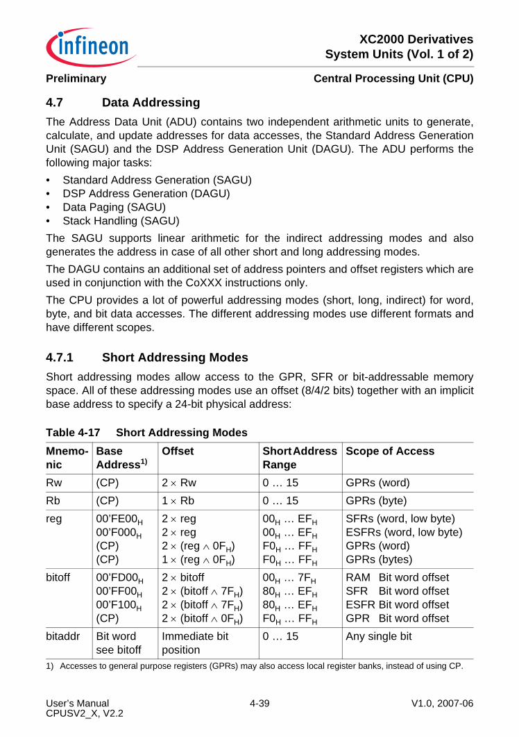
XC2000 DerivativesSystem Units (Vol. 1 of 2)
Central Processing Unit (CPU)Preliminary
4.7 Data AddressingThe Address Data Unit (ADU) contains two independent arithmetic units to generate,calculate, and update addresses for data accesses, the Standard Address GenerationUnit (SAGU) and the DSP Address Generation Unit (DAGU). The ADU performs thefollowing major tasks:• Standard Address Generation (SAGU)• DSP Address Generation (DAGU)• Data Paging (SAGU)• Stack Handling (SAGU)The SAGU supports linear arithmetic for the indirect addressing modes and alsogenerates the address in case of all other short and long addressing modes.The DAGU contains an additional set of address pointers and offset registers which areused in conjunction with the CoXXX instructions only.The CPU provides a lot of powerful addressing modes (short, long, indirect) for word,byte, and bit data accesses. The different addressing modes use different formats andhave different scopes.
4.7.1 Short Addressing ModesShort addressing modes allow access to the GPR, SFR or bit-addressable memoryspace. All of these addressing modes use an offset (8/4/2 bits) together with an implicitbase address to specify a 24-bit physical address:
Table 4-17 Short Addressing ModesMnemo-nic
Base Address1)
1) Accesses to general purpose registers (GPRs) may also access local register banks, instead of using CP.
Offset Short Address Range
Scope of Access
Rw (CP) 2 × Rw 0 … 15 GPRs (word)Rb (CP) 1 × Rb 0 … 15 GPRs (byte)reg 00’FE00H
00’F000H(CP)(CP)
2 × reg2 × reg2 × (reg ∧ 0FH)1 × (reg ∧ 0FH)
00H … EFH00H … EFHF0H … FFHF0H … FFH
SFRs (word, low byte)ESFRs (word, low byte)GPRs (word)GPRs (bytes)
bitoff 00’FD00H00’FF00H00’F100H(CP)
2 × bitoff2 × (bitoff ∧ 7FH)2 × (bitoff ∧ 7FH)2 × (bitoff ∧ 0FH)
00H … 7FH80H … EFH80H … EFHF0H … FFH
RAM Bit word offsetSFR Bit word offsetESFR Bit word offsetGPR Bit word offset
bitaddr Bit word see bitoff
Immediate bit position
0 … 15 Any single bit
User’s Manual 4-39 V1.0, 2007-06CPUSV2_X, V2.2
XC2000 DerivativesSystem Units (Vol. 1 of 2)
Central Processing Unit (CPU)Preliminary
Physical Address = Base Address + ∆ × Short AddressNote: ∆ is 1 for byte GPRs, ∆ is 2 for word GPRs.
Rw, Rb: Specifies direct access to any GPR in the currently active context (globalregister bank or local register bank). Both ‘Rw’ and ‘Rb’ require four bits in the instructionformat. The base address of the global register bank is determined by the contents ofregister CP. ‘Rw’ specifies a 4-bit word GPR address, ‘Rb’ specifies a 4-bit byte GPRaddress within a local register bank or relative to (CP).reg: Specifies direct access to any (E)SFR or GPR in the currently active context (globalor local register bank). The ‘reg’ value requires eight bits in the instruction format. Short‘reg’ addresses in the range from 00H to EFH always specify (E)SFRs. In that case, thefactor ‘∆’ equates 2 and the base address is 00’FE00H for the standard SFR area or00’F000H for the extended ESFR area. The ‘reg’ accesses to the ESFR area require apreceding EXT*R instruction to switch the base address. Depending on the opcode,either the total word (for word operations) or the low byte (for byte operations) of an SFRcan be addressed via ‘reg’. Note that the high byte of an SFR cannot be accessed viathe ‘reg’ addressing mode. Short ‘reg’ addresses in the range from F0H to FFH alwaysspecify GPRs. In that case, only the lower four bits of ‘reg’ are significant for physicaladdress generation and, therefore, it is identical to the address generation described forthe ‘Rb’ and ‘Rw’ addressing modes.bitoff: Specifies direct access to any word in the bit addressable memory space. The‘bitoff’ value requires eight bits in the instruction format. The specified ‘bitoff’ rangeselects different base addresses to generate physical addresses (see Table 4-17). The‘bitoff’ accesses to the ESFR area require a preceding EXT*R instruction to switch thebase address.bitaddr: Any bit address is specified by a word address within the bit addressablememory space (see ‘bitoff’) and a bit position (‘bitpos’) within that word. Therefore,‘bitaddr’ requires twelve bits in the instruction format.
User’s Manual 4-40 V1.0, 2007-06CPUSV2_X, V2.2
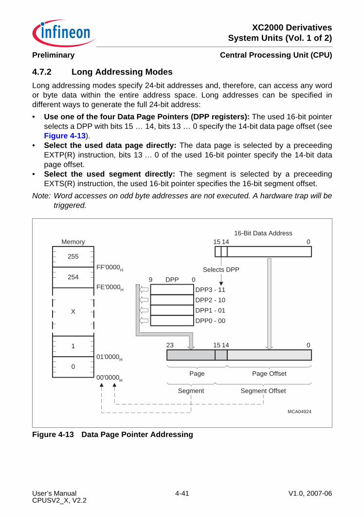
XC2000 DerivativesSystem Units (Vol. 1 of 2)
Central Processing Unit (CPU)Preliminary
4.7.2 Long Addressing ModesLong addressing modes specify 24-bit addresses and, therefore, can access any wordor byte data within the entire address space. Long addresses can be specified indifferent ways to generate the full 24-bit address:• Use one of the four Data Page Pointers (DPP registers): The used 16-bit pointer
selects a DPP with bits 15 … 14, bits 13 … 0 specify the 14-bit data page offset (seeFigure 4-13).
• Select the used data page directly: The data page is selected by a preceedingEXTP(R) instruction, bits 13 … 0 of the used 16-bit pointer specify the 14-bit datapage offset.
• Select the used segment directly: The segment is selected by a preceedingEXTS(R) instruction, the used 16-bit pointer specifies the 16-bit segment offset.
Note: Word accesses on odd byte addresses are not executed. A hardware trap will betriggered.
Figure 4-13 Data Page Pointer Addressing
MCA04924
9 0DPP
DPP3 - 11
DPP2 - 10
DPP1 - 01
DPP0 - 00
16-Bit Data Address
Selects DPP
23 15 14 0
Page Page Offset
Segment Segment Offset
Memory
255
254
1
0
X
FF'0000H
FE'0000H
01'0000H
00'0000H
015 14
User’s Manual 4-41 V1.0, 2007-06CPUSV2_X, V2.2
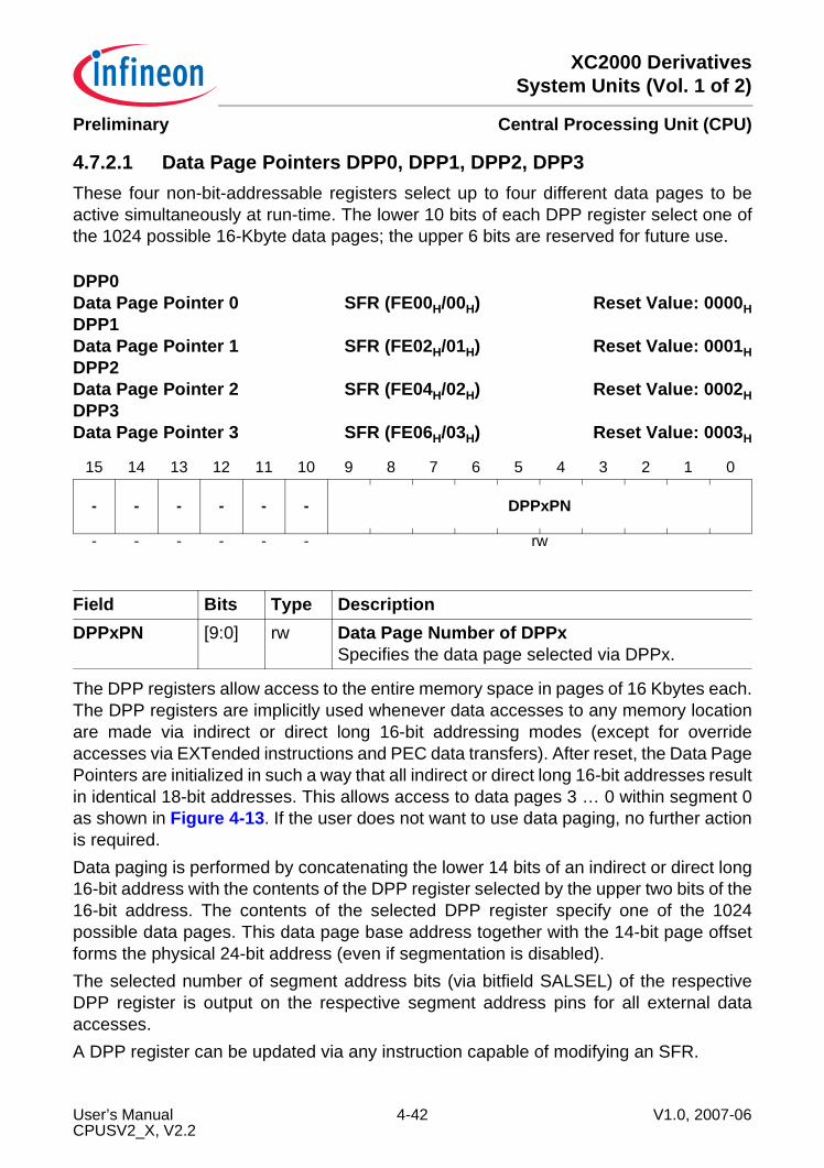
XC2000 DerivativesSystem Units (Vol. 1 of 2)
Central Processing Unit (CPU)Preliminary
4.7.2.1 Data Page Pointers DPP0, DPP1, DPP2, DPP3These four non-bit-addressable registers select up to four different data pages to beactive simultaneously at run-time. The lower 10 bits of each DPP register select one ofthe 1024 possible 16-Kbyte data pages; the upper 6 bits are reserved for future use.
The DPP registers allow access to the entire memory space in pages of 16 Kbytes each.The DPP registers are implicitly used whenever data accesses to any memory locationare made via indirect or direct long 16-bit addressing modes (except for overrideaccesses via EXTended instructions and PEC data transfers). After reset, the Data PagePointers are initialized in such a way that all indirect or direct long 16-bit addresses resultin identical 18-bit addresses. This allows access to data pages 3 … 0 within segment 0as shown in Figure 4-13. If the user does not want to use data paging, no further actionis required.Data paging is performed by concatenating the lower 14 bits of an indirect or direct long16-bit address with the contents of the DPP register selected by the upper two bits of the16-bit address. The contents of the selected DPP register specify one of the 1024possible data pages. This data page base address together with the 14-bit page offsetforms the physical 24-bit address (even if segmentation is disabled).The selected number of segment address bits (via bitfield SALSEL) of the respectiveDPP register is output on the respective segment address pins for all external dataaccesses.A DPP register can be updated via any instruction capable of modifying an SFR.
DPP0 Data Page Pointer 0 SFR (FE00H/00H) Reset Value: 0000HDPP1Data Page Pointer 1 SFR (FE02H/01H) Reset Value: 0001HDPP2Data Page Pointer 2 SFR (FE04H/02H) Reset Value: 0002HDPP3Data Page Pointer 3 SFR (FE06H/03H) Reset Value: 0003H
15 14 13 12 11 10 9 8 7 6 5 4 3 2 1 0
- - - - - - DPPxPN
- - - - - - rw
Field Bits Type DescriptionDPPxPN [9:0] rw Data Page Number of DPPx
Specifies the data page selected via DPPx.
User’s Manual 4-42 V1.0, 2007-06CPUSV2_X, V2.2
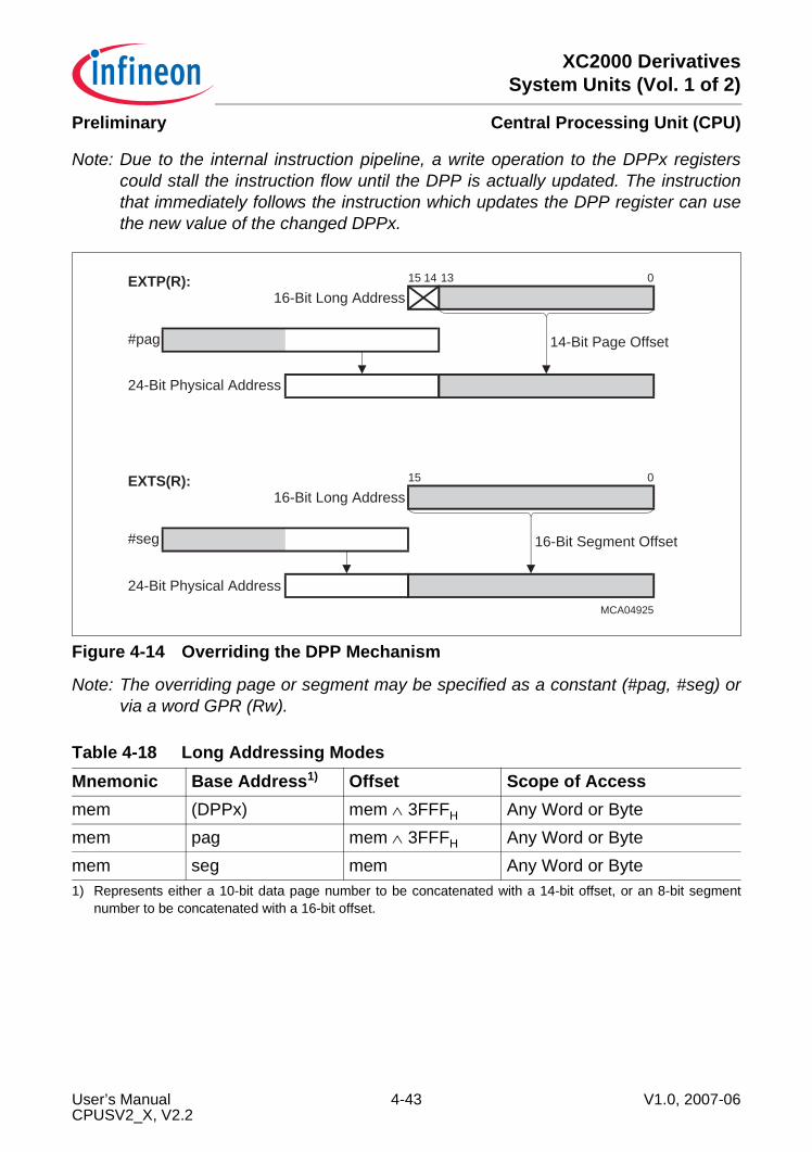
XC2000 DerivativesSystem Units (Vol. 1 of 2)
Central Processing Unit (CPU)Preliminary
Note: Due to the internal instruction pipeline, a write operation to the DPPx registerscould stall the instruction flow until the DPP is actually updated. The instructionthat immediately follows the instruction which updates the DPP register can usethe new value of the changed DPPx.
Figure 4-14 Overriding the DPP Mechanism
Note: The overriding page or segment may be specified as a constant (#pag, #seg) orvia a word GPR (Rw).
Table 4-18 Long Addressing ModesMnemonic Base Address1)
1) Represents either a 10-bit data page number to be concatenated with a 14-bit offset, or an 8-bit segmentnumber to be concatenated with a 16-bit offset.
Offset Scope of Accessmem (DPPx) mem ∧ 3FFFH Any Word or Bytemem pag mem ∧ 3FFFH Any Word or Bytemem seg mem Any Word or Byte
MCA04925
15 14 13
14-Bit Page Offset
16-Bit Segment Offset
#pag
#seg
0
15 0
24-Bit Physical Address
24-Bit Physical Address
16-Bit Long Address
16-Bit Long AddressEXTS(R):
EXTP(R):
User’s Manual 4-43 V1.0, 2007-06CPUSV2_X, V2.2
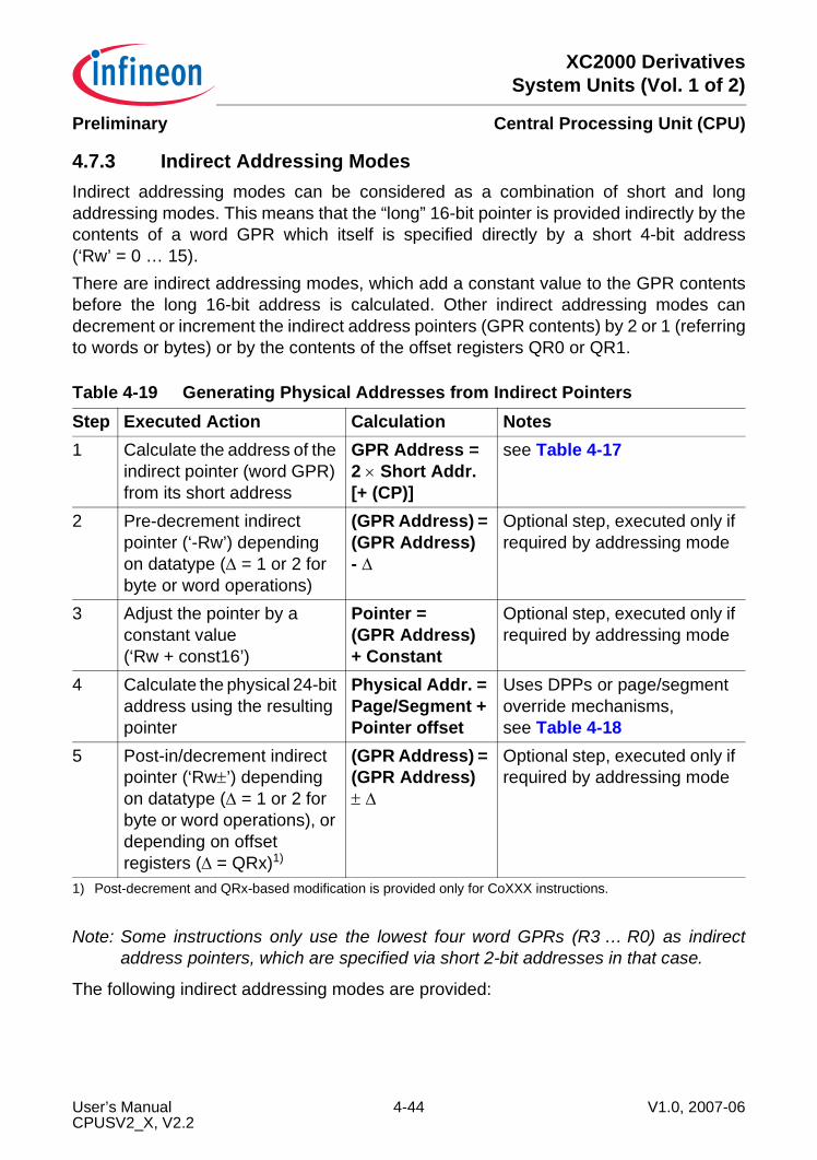
XC2000 DerivativesSystem Units (Vol. 1 of 2)
Central Processing Unit (CPU)Preliminary
4.7.3 Indirect Addressing ModesIndirect addressing modes can be considered as a combination of short and longaddressing modes. This means that the “long” 16-bit pointer is provided indirectly by thecontents of a word GPR which itself is specified directly by a short 4-bit address(‘Rw’ = 0 … 15).There are indirect addressing modes, which add a constant value to the GPR contentsbefore the long 16-bit address is calculated. Other indirect addressing modes candecrement or increment the indirect address pointers (GPR contents) by 2 or 1 (referringto words or bytes) or by the contents of the offset registers QR0 or QR1.
Note: Some instructions only use the lowest four word GPRs (R3 … R0) as indirectaddress pointers, which are specified via short 2-bit addresses in that case.
The following indirect addressing modes are provided:
Table 4-19 Generating Physical Addresses from Indirect PointersStep Executed Action Calculation Notes1 Calculate the address of the
indirect pointer (word GPR) from its short address
GPR Address = 2 × Short Addr. [+ (CP)]
see Table 4-17
2 Pre-decrement indirect pointer (‘-Rw’) depending on datatype (∆ = 1 or 2 for byte or word operations)
(GPR Address) = (GPR Address) - ∆
Optional step, executed only if required by addressing mode
3 Adjust the pointer by a constant value (‘Rw + const16’)
Pointer = (GPR Address) + Constant
Optional step, executed only if required by addressing mode
4 Calculate the physical 24-bit address using the resulting pointer
Physical Addr. = Page/Segment + Pointer offset
Uses DPPs or page/segment override mechanisms,see Table 4-18
5 Post-in/decrement indirect pointer (‘Rw±’) depending on datatype (∆ = 1 or 2 for byte or word operations), or depending on offset registers (∆ = QRx)1)
1) Post-decrement and QRx-based modification is provided only for CoXXX instructions.
(GPR Address) = (GPR Address) ± ∆
Optional step, executed only if required by addressing mode
User’s Manual 4-44 V1.0, 2007-06CPUSV2_X, V2.2
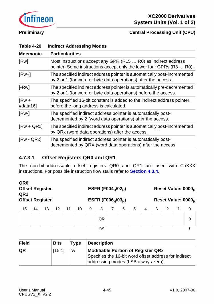
XC2000 DerivativesSystem Units (Vol. 1 of 2)
Central Processing Unit (CPU)Preliminary
4.7.3.1 Offset Registers QR0 and QR1The non-bit-addressable offset registers QR0 and QR1 are used with CoXXXinstructions. For possible instruction flow stalls refer to Section 4.3.4.
Table 4-20 Indirect Addressing ModesMnemonic Particularities[Rw] Most instructions accept any GPR (R15 … R0) as indirect address
pointer. Some instructions accept only the lower four GPRs (R3 … R0).[Rw+] The specified indirect address pointer is automatically post-incremented
by 2 or 1 (for word or byte data operations) after the access.[-Rw] The specified indirect address pointer is automatically pre-decremented
by 2 or 1 (for word or byte data operations) before the access.[Rw + #data16]
The specified 16-bit constant is added to the indirect address pointer, before the long address is calculated.
[Rw-] The specified indirect address pointer is automatically post-decremented by 2 (word data operations) after the access.
[Rw + QRx] The specified indirect address pointer is automatically post-incremented by QRx (word data operations) after the access.
[Rw - QRx] The specified indirect address pointer is automatically post-decremented by QRX (word data operations) after the access.
QR0 Offset Register ESFR (F004H/02H) Reset Value: 0000HQR1Offset Register ESFR (F006H/03H) Reset Value: 0000H
15 14 13 12 11 10 9 8 7 6 5 4 3 2 1 0
QR 0
rw r
Field Bits Type DescriptionQR [15:1] rw Modifiable Portion of Register QRx
Specifies the 16-bit word offset address for indirect addressing modes (LSB always zero).
User’s Manual 4-45 V1.0, 2007-06CPUSV2_X, V2.2
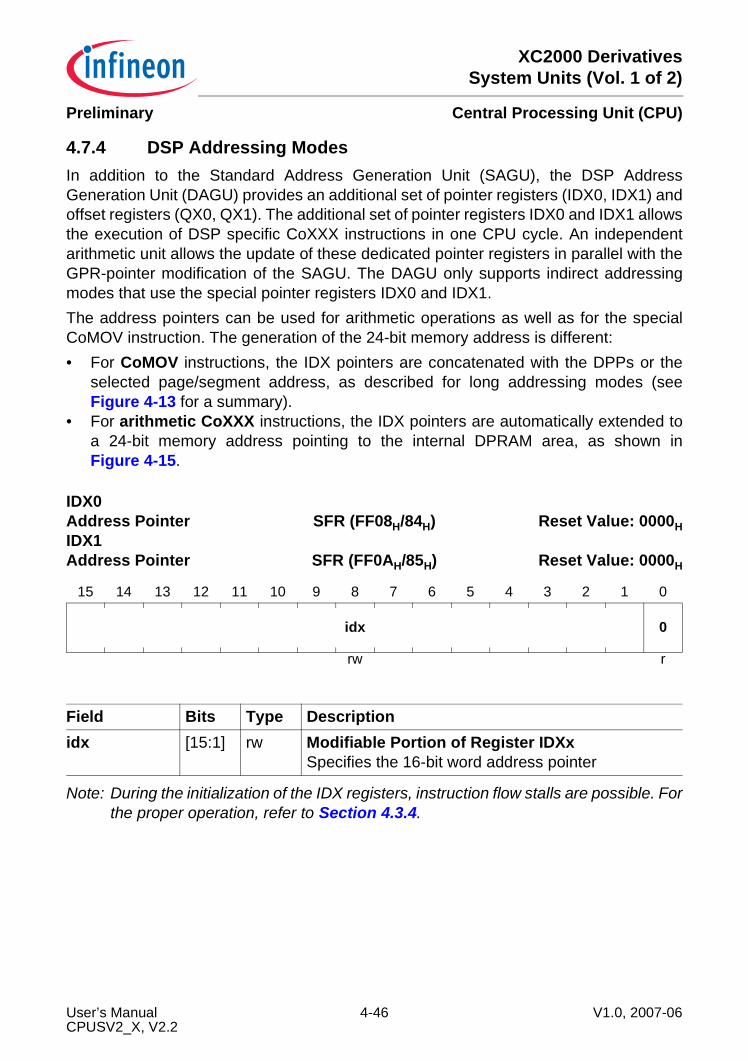
XC2000 DerivativesSystem Units (Vol. 1 of 2)
Central Processing Unit (CPU)Preliminary
4.7.4 DSP Addressing ModesIn addition to the Standard Address Generation Unit (SAGU), the DSP AddressGeneration Unit (DAGU) provides an additional set of pointer registers (IDX0, IDX1) andoffset registers (QX0, QX1). The additional set of pointer registers IDX0 and IDX1 allowsthe execution of DSP specific CoXXX instructions in one CPU cycle. An independentarithmetic unit allows the update of these dedicated pointer registers in parallel with theGPR-pointer modification of the SAGU. The DAGU only supports indirect addressingmodes that use the special pointer registers IDX0 and IDX1.The address pointers can be used for arithmetic operations as well as for the specialCoMOV instruction. The generation of the 24-bit memory address is different:• For CoMOV instructions, the IDX pointers are concatenated with the DPPs or the
selected page/segment address, as described for long addressing modes (seeFigure 4-13 for a summary).
• For arithmetic CoXXX instructions, the IDX pointers are automatically extended toa 24-bit memory address pointing to the internal DPRAM area, as shown inFigure 4-15.
Note: During the initialization of the IDX registers, instruction flow stalls are possible. Forthe proper operation, refer to Section 4.3.4.
IDX0 Address Pointer SFR (FF08H/84H) Reset Value: 0000HIDX1Address Pointer SFR (FF0AH/85H) Reset Value: 0000H
15 14 13 12 11 10 9 8 7 6 5 4 3 2 1 0
idx 0
rw r
Field Bits Type Descriptionidx [15:1] rw Modifiable Portion of Register IDXx
Specifies the 16-bit word address pointer
User’s Manual 4-46 V1.0, 2007-06CPUSV2_X, V2.2
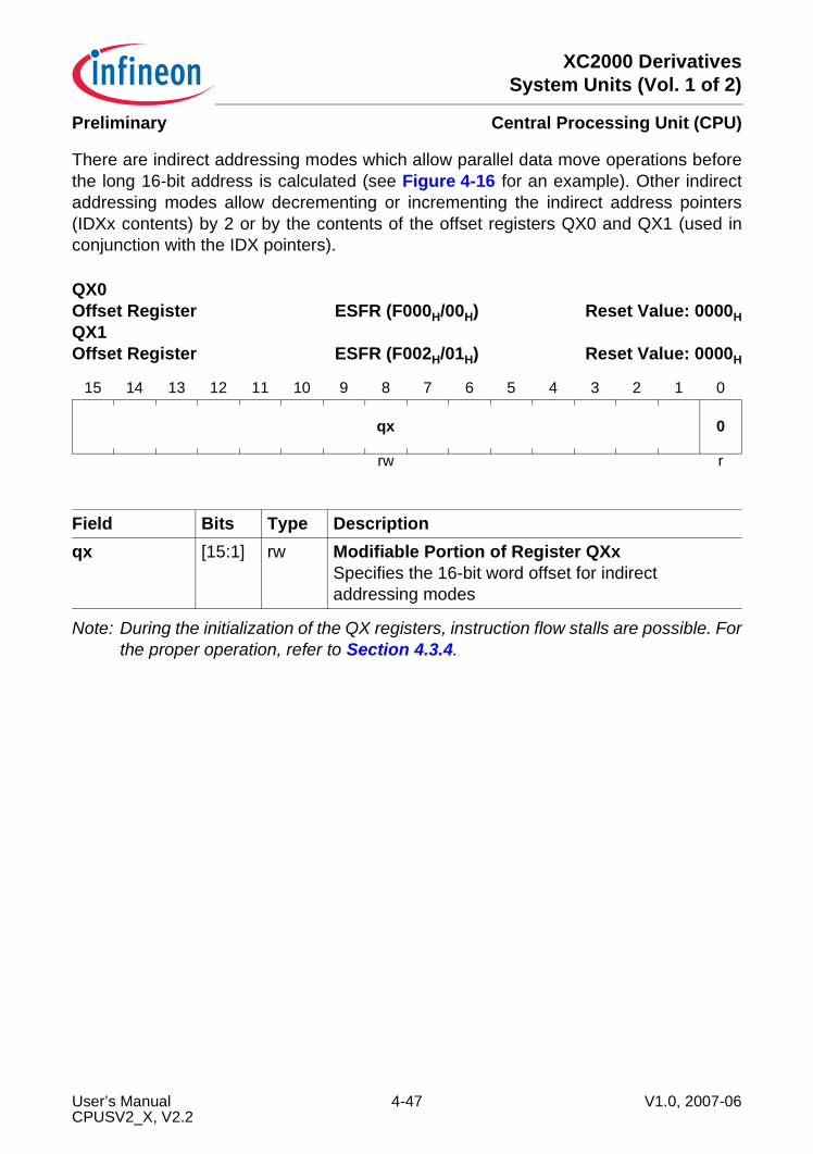
XC2000 DerivativesSystem Units (Vol. 1 of 2)
Central Processing Unit (CPU)Preliminary
There are indirect addressing modes which allow parallel data move operations beforethe long 16-bit address is calculated (see Figure 4-16 for an example). Other indirectaddressing modes allow decrementing or incrementing the indirect address pointers(IDXx contents) by 2 or by the contents of the offset registers QX0 and QX1 (used inconjunction with the IDX pointers).
Note: During the initialization of the QX registers, instruction flow stalls are possible. Forthe proper operation, refer to Section 4.3.4.
QX0 Offset Register ESFR (F000H/00H) Reset Value: 0000HQX1Offset Register ESFR (F002H/01H) Reset Value: 0000H
15 14 13 12 11 10 9 8 7 6 5 4 3 2 1 0
qx 0
rw r
Field Bits Type Descriptionqx [15:1] rw Modifiable Portion of Register QXx
Specifies the 16-bit word offset for indirect addressing modes
User’s Manual 4-47 V1.0, 2007-06CPUSV2_X, V2.2
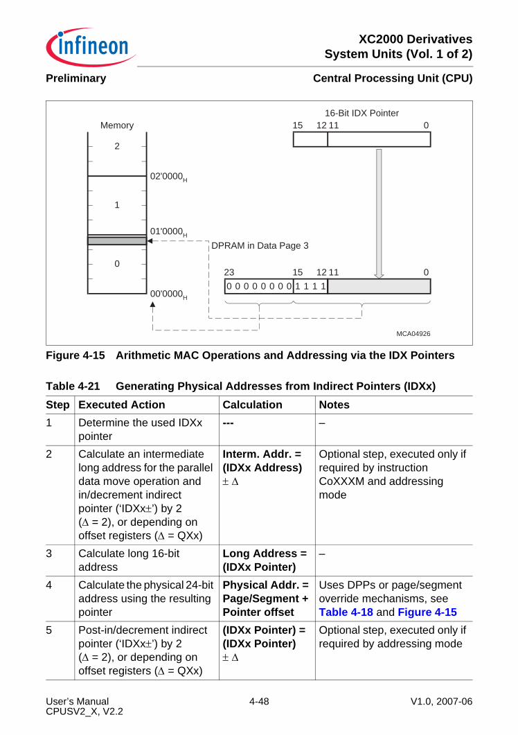
XC2000 DerivativesSystem Units (Vol. 1 of 2)
Central Processing Unit (CPU)Preliminary
Figure 4-15 Arithmetic MAC Operations and Addressing via the IDX Pointers
Table 4-21 Generating Physical Addresses from Indirect Pointers (IDXx)Step Executed Action Calculation Notes1 Determine the used IDXx
pointer--- –
2 Calculate an intermediate long address for the parallel data move operation and in/decrement indirect pointer (‘IDXx±’) by 2 (∆ = 2), or depending on offset registers (∆ = QXx)
Interm. Addr. = (IDXx Address) ± ∆
Optional step, executed only if required by instruction CoXXXM and addressing mode
3 Calculate long 16-bit address
Long Address = (IDXx Pointer)
–
4 Calculate the physical 24-bit address using the resulting pointer
Physical Addr. = Page/Segment + Pointer offset
Uses DPPs or page/segment override mechanisms, see Table 4-18 and Figure 4-15
5 Post-in/decrement indirect pointer (‘IDXx±’) by 2 (∆ = 2), or depending on offset registers (∆ = QXx)
(IDXx Pointer) = (IDXx Pointer) ± ∆
Optional step, executed only if required by addressing mode
023
0
2
MCA04926
16-Bit IDX Pointer
15 12
Memory
02'0000H
11
11
01'0000H
00'0000H
DPRAM in Data Page 3
1
0
10 111000000
15 12 0
User’s Manual 4-48 V1.0, 2007-06CPUSV2_X, V2.2
XC2000 DerivativesSystem Units (Vol. 1 of 2)
Central Processing Unit (CPU)Preliminary
The following indirect addressing modes are provided:
Note: An example for parallel data move operations can be found in Figure 4-16.
Table 4-22 DSP Addressing ModesMnemonic Particularities[IDXx] Most CoXXX instructions accept IDXx (IDX0, IDX1) as an indirect
address pointer.[IDXx+] The specified indirect address pointer is automatically post-incremented
by 2 after the access.with parallel data move
In case of a CoXXXM instruction, the address stored in the specified indirect address pointer is automatically pre-decremented by 2 for the parallel move operation. The pointer itself is not pre-decremented. Then, the specified indirect address pointer is automatically post-incremented by 2 after the access.
[IDXx-] The specified indirect address pointer is automatically post-decremented by 2 after the access.
with parallel data move
In case of a CoXXXM instruction, the address stored in the specified indirect address pointer is automatically pre-incremented by 2 for the parallel move operation. The pointer itself is not pre-incremented. Then, the specified indirect address pointer is automatically post-decremented by 2 after the access.
[IDXx + QXx] The specified indirect address pointer is automatically post-incremented by QXx after the access.
with parallel data move
In case of a CoXXXM instruction, the address stored in the specified indirect address pointer is automatically pre-decremented by QXx for the parallel move operation. The pointer itself is not pre-decremented. Then, the specified indirect address pointer is automatically post-incremented by QXx after the access.
[IDXx - QXx] The specified indirect address pointer is automatically post-decremented by QXx after the access.
with parallel data move
In case of a CoXXXM instruction, the address stored in the specified indirect address pointer is automatically pre-incremented by QXx for the parallel move operation. The pointer itself is not pre-incremented. Then, the specified indirect address pointer is automatically post-decremented by QXx after the access.
User’s Manual 4-49 V1.0, 2007-06CPUSV2_X, V2.2
XC2000 DerivativesSystem Units (Vol. 1 of 2)
Central Processing Unit (CPU)Preliminary
The CoREG Addressing ModeThe CoSTORE instruction utilizes the special CoREG addressing mode for immediatestorage of the MAC-Unit register after a MAC operation. The address of the MAC-Unitregister is coded in the CoSTORE instruction format as described in Table 4-23:
The example in Figure 4-16 shows the complex operation of CoXXXM instructions witha parallel move operation based on the descriptions about addressing modes given inSection 4.7.3 (Indirect Addressing Modes) and Section 4.7.4 (DSP AddressingModes).
Table 4-23 Coding of the CoREG Addressing ModeMnemonic Register Coding of wwww:w bits [31:27]MSW MAC-Unit Status Word 00000MAH MAC-Unit Accumulator High Word 00001MAS Limited MAC-Unit Accumulator High
Word00010
MAL MAC-Unit Accumulator Low Word 00100MCW MAC-Unit Control Word 00101MRW MAC-Unit Repeat Word 00110
User’s Manual 4-50 V1.0, 2007-06CPUSV2_X, V2.2
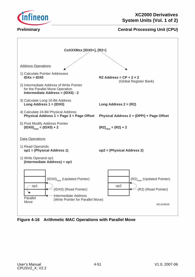
XC2000 DerivativesSystem Units (Vol. 1 of 2)
Central Processing Unit (CPU)Preliminary
Figure 4-16 Arithmetic MAC Operations with Parallel Move
MCA04928
Address Operations
1) Calculate Pointer Addresses IDXx = IDX0 R2 Address = CP + 2 × 2
(Global Register Bank)2) Intermediate Address of Write Pointer for the Parallel Move Operation Intermediate Address = (IDX0) - 2
3) Calculate Long 16-Bit Address Long Address 1 = (IDX0) Long Address 2 = (R2)
4) Calculate 24-Bit Physical Address Physical Address 1 = Page 3 + Page Offset Physical Address 2 = (DPPi) + Page Offset
5) Post Modify Address Pointer (IDX0)new = (IDX0) + 2 (R2)new = (R2) + 2
Data Operations
1) Read Operands op1 = (Physical Address 1) op2 = (Physical Address 2)
1) Write Operand op1 (Intermediate Address) = op1
CoXXXMxx [IDX0+], [R2+]
op1
ParallelMove
(IDX0)new (Updated Pointer)
(IDX0) (Read Pointer)
Intermediate Address(Write Pointer for Parallel Move)
op2
(R2)new (Updated Pointer)
(R2) (Read Pointer)
User’s Manual 4-51 V1.0, 2007-06CPUSV2_X, V2.2
XC2000 DerivativesSystem Units (Vol. 1 of 2)
Central Processing Unit (CPU)Preliminary
4.7.5 The System StackThe XC2000 supports a system stack of up to 64 Kbytes. The stack can be locatedinternally in one of the on-chip memories or externally. The 16-bit Stack Pointer register(SP) addresses the stack within a 64-Kbyte segment selected by the Stack PointerSegment register (SPSG). A virtual stack (usually bigger than 64 Kbytes) can beimplemented by software. This mechanism is supported by the Stack Overflow registerSTKOV and the Stack Underflow register STKUN (see descriptions below).
4.7.5.1 The Stack Pointer Registers SP and SPSEG Register SPSEG (not bitaddressable) selects the segment being used at run-time toaccess the system stack. The lower eight bits of register SPSEG select one of up256 segments of 64 Kbytes each, while the higher 8 bits are reserved for future use.The Stack Pointer SP (not bitaddressable) points to the top of the system stack (TOS).SP is pre-decremented whenever data is pushed onto the stack, and it is post-incremented whenever data is popped from the stack. Therefore, the system stackgrows from higher towards lower memory locations.System stack addresses are generated by directly extending the 16-bit contents ofregister SP by the contents of register SPSG, as shown in Figure 4-17.The system stack cannot cross a 64-Kbyte segment boundary.
Figure 4-17 Addressing via the Stack Pointer
15
MCA04929
23 0
Stack PointerSegment
255
254
1
0
FF'0000H
FE'0000H
01'0000H
00'0000H
16
15 0SP15 0SPSEGNR7
SPSEG
User’s Manual 4-52 V1.0, 2007-06CPUSV2_X, V2.2
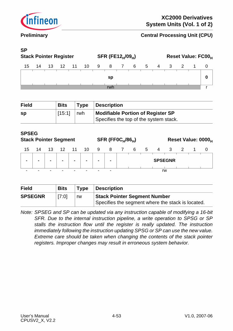
XC2000 DerivativesSystem Units (Vol. 1 of 2)
Central Processing Unit (CPU)Preliminary
Note: SPSEG and SP can be updated via any instruction capable of modifying a 16-bitSFR. Due to the internal instruction pipeline, a write operation to SPSG or SPstalls the instruction flow until the register is really updated. The instructionimmediately following the instruction updating SPSG or SP can use the new value.Extreme care should be taken when changing the contents of the stack pointerregisters. Improper changes may result in erroneous system behavior.
SP Stack Pointer Register SFR (FE12H/09H) Reset Value: FC00H
15 14 13 12 11 10 9 8 7 6 5 4 3 2 1 0
sp 0
rwh r
Field Bits Type Descriptionsp [15:1] rwh Modifiable Portion of Register SP
Specifies the top of the system stack.
SPSEG Stack Pointer Segment SFR (FF0CH/86H) Reset Value: 0000H
15 14 13 12 11 10 9 8 7 6 5 4 3 2 1 0
- - - - - - - - SPSEGNR
- - - - - - - - rw
Field Bits Type DescriptionSPSEGNR [7:0] rw Stack Pointer Segment Number
Specifies the segment where the stack is located.
User’s Manual 4-53 V1.0, 2007-06CPUSV2_X, V2.2

XC2000 DerivativesSystem Units (Vol. 1 of 2)
Central Processing Unit (CPU)Preliminary
4.7.5.2 The Stack Overflow/Underflow Pointers STKOV/STKUNThese limit registers (not bit-addressable) supervise the stack pointer. A trap isgenerated when the stack pointer reaches its upper or lower limit. The Stack PointerSegment Register SPSG is not taken into account for the stack pointer comparison. Thesystem stack cannot cross a 64-Kbyte segment.STKOV is compared with SP before each implicit write operation which decrements thecontents of SP (instructions CALLA, CALLI, CALLR, CALLS, PCALL, TRAP, SCXT, orPUSH). If the contents of SP are equal to the contents of STKOV a stack overflow trapis triggered.STKUN is compared with SP before each implicit read operation which increments thecontents of SP (instructions RET, RETS, RETP, RETI, or POP). If the contents of SP areequal to the contents of STKUN a stack underflow trap is triggered.The Stack Overflow/Underflow Traps may be used in two different ways:• Fatal error indication treats the stack overflow as a system error and executes the
associated trap service routine.In case of a stack overflow trap, data in the bottom of the stack may have beenoverwritten by the status information stacked upon servicing the trap itself.
• Virtual stack control allows the system stack to be used as a ‘Stack Cache’ for abigger external user stack: flush cache in case of an overflow, refill cache in case ofan underflow.
Scope of Stack Limit ControlThe stack limit control implemented by the register pair STKOV and STKUN detectscases in which the Stack Pointer (SP) crosses the defined stack area as a result of animplicit change.If the stack pointer was explicitly changed as a result of move or arithmetic instruction,SP is not compared to the contents of STKOV and STKUN. In this case, a stack violationwill not be detected if the modified stack pointer is on or outside the defined limits, i.e.below (STKOV) or above (STKUN). Stack overflow/underflow is detected only in case ofimplicit SP modification.SP may be operated outside the permitted SP range without triggering a trap. However,if SP reaches the limit of the permitted SP range from outside the range as a result of animplicit change (PUSH or POP, for example), the respective trap will be triggered.Note: STKOV and STKUN can be updated via any instruction capable of modifying an
SFR. If a stack overflow or underflow event occurs in an ATOMIC/EXT sequence,the stack operations that are part of the sequence are completed. The trap isissued after the completion of the entire ATOMIC/EXT sequence.
User’s Manual 4-54 V1.0, 2007-06CPUSV2_X, V2.2
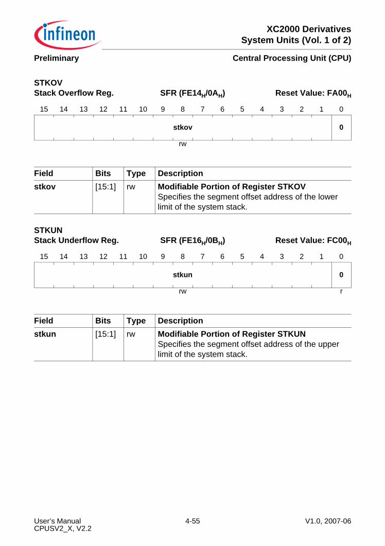
XC2000 DerivativesSystem Units (Vol. 1 of 2)
Central Processing Unit (CPU)Preliminary
STKOV Stack Overflow Reg. SFR (FE14H/0AH) Reset Value: FA00H
15 14 13 12 11 10 9 8 7 6 5 4 3 2 1 0
stkov 0
rw
Field Bits Type Descriptionstkov [15:1] rw Modifiable Portion of Register STKOV
Specifies the segment offset address of the lower limit of the system stack.
STKUN Stack Underflow Reg. SFR (FE16H/0BH) Reset Value: FC00H
15 14 13 12 11 10 9 8 7 6 5 4 3 2 1 0
stkun 0
rw r
Field Bits Type Descriptionstkun [15:1] rw Modifiable Portion of Register STKUN
Specifies the segment offset address of the upper limit of the system stack.
User’s Manual 4-55 V1.0, 2007-06CPUSV2_X, V2.2
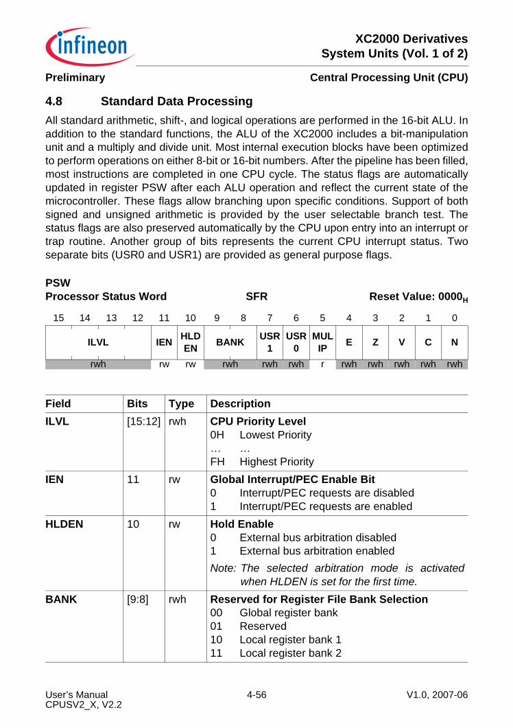
XC2000 DerivativesSystem Units (Vol. 1 of 2)
Central Processing Unit (CPU)Preliminary
4.8 Standard Data ProcessingAll standard arithmetic, shift-, and logical operations are performed in the 16-bit ALU. Inaddition to the standard functions, the ALU of the XC2000 includes a bit-manipulationunit and a multiply and divide unit. Most internal execution blocks have been optimizedto perform operations on either 8-bit or 16-bit numbers. After the pipeline has been filled,most instructions are completed in one CPU cycle. The status flags are automaticallyupdated in register PSW after each ALU operation and reflect the current state of themicrocontroller. These flags allow branching upon specific conditions. Support of bothsigned and unsigned arithmetic is provided by the user selectable branch test. Thestatus flags are also preserved automatically by the CPU upon entry into an interrupt ortrap routine. Another group of bits represents the current CPU interrupt status. Twoseparate bits (USR0 and USR1) are provided as general purpose flags.
PSW Processor Status Word SFR Reset Value: 0000H
15 14 13 12 11 10 9 8 7 6 5 4 3 2 1 0
ILVL IEN HLDEN BANK USR
1USR
0MUL
IP E Z V C N
rwh rw rw rwh rwh rwh r rwh rwh rwh rwh rwh
Field Bits Type DescriptionILVL [15:12] rwh CPU Priority Level
0H Lowest Priority… …FH Highest Priority
IEN 11 rw Global Interrupt/PEC Enable Bit0 Interrupt/PEC requests are disabled1 Interrupt/PEC requests are enabled
HLDEN 10 rw Hold Enable0 External bus arbitration disabled1 External bus arbitration enabledNote: The selected arbitration mode is activated
when HLDEN is set for the first time.BANK [9:8] rwh Reserved for Register File Bank Selection
00 Global register bank01 Reserved10 Local register bank 111 Local register bank 2
User’s Manual 4-56 V1.0, 2007-06CPUSV2_X, V2.2
XC2000 DerivativesSystem Units (Vol. 1 of 2)
Central Processing Unit (CPU)Preliminary
ALU/MAC Status (N, C, V, Z, E, USR0, USR1)The condition flags (N, C, V, Z, E) within the PSW indicate the ALU status after the mostrecently performed ALU operation. They are set by most of the instructions according tospecific rules which depend on the ALU or data movement operation performed by aninstruction.After execution of an instruction which explicitly updates the PSW register, the conditionflags cannot be interpreted as described below because any explicit write to the PSWregister supersedes the condition flag values which are implicitly generated by the CPU.Explicitly reading the PSW register supplies a read value which represents the state ofthe PSW register after execution of the immediately preceding instruction.Note: After reset, all of the ALU status bits are cleared.
N-Flag: For most of the ALU operations, the N-flag is set to 1, if the most significant bitof the result contains a 1; otherwise, it is cleared. In the case of integer operations, theN-flag can be interpreted as the sign bit of the result (negative: N = 1, positive: N = 0).
USR1 7 rwh General Purpose FlagMay be used by application
USR0 6 rwh General Purpose FlagMay be used by application
MULIP 5 r Multiplication/Division in ProgressNote: Always set to 0 (MUL/DIV not interruptible),
for compatibility with existing software.E 4 rwh End of Table Flag
0 Source operand is neither 8000H nor 80H1 Source operand is 8000H or 80H
Z 3 rwh Zero Flag0 ALU result is not zero1 ALU result is zero
V 2 rwh Overflow Flag0 No Overflow produced1 Overflow produced
C 1 rwh Carry Flag0 No carry/borrow bit produced1 Carry/borrow bit produced
N 0 rwh Negative Result0 ALU result is not negative1 ALU result is negative
Field Bits Type Description
User’s Manual 4-57 V1.0, 2007-06CPUSV2_X, V2.2
XC2000 DerivativesSystem Units (Vol. 1 of 2)
Central Processing Unit (CPU)Preliminary
Negative numbers are always represented as the 2’s complement of the correspondingpositive number. The range of signed numbers extends from -8000H to +7FFFH for theword data type, or from -80H to +7FH for the byte data type. For Boolean bit operationswith only one operand, the N-flag represents the previous state of the specified bit. ForBoolean bit operations with two operands, the N-flag represents the logical XORing ofthe two specified bits.C-Flag: After an addition, the C-flag indicates that a carry from the most significant bit ofthe specified word or byte data type has been generated. After a subtraction or acomparison, the C-flag indicates a borrow which represents the logical negation of acarry for the addition.This means that the C-flag is set to 1, if no carry from the most significant bit of thespecified word or byte data type has been generated during a subtraction, which isperformed internally by the ALU as a 2’s complement addition, and, the C-flag is clearedwhen this complement addition caused a carry.The C-flag is always cleared for logical, multiply and divide ALU operations, becausethese operations cannot cause a carry.For shift and rotate operations, the C-flag represents the value of the bit shifted out last.If a shift count of zero is specified, the C-flag will be cleared. The C-flag is also clearedfor a prioritize ALU operation, because a 1 is never shifted out of the MSB during thenormalization of an operand.For Boolean bit operations with only one operand, the C-flag is always cleared. ForBoolean bit operations with two operands, the C-flag represents the logical ANDing ofthe two specified bits.V-Flag: For addition, subtraction, and 2’s complementation, the V-flag is always set to 1if the result exceeds the range of 16-bit signed numbers for word operations (-8000H to+7FFFH), or 8-bit signed numbers for byte operations (-80H to +7FH). Otherwise, theV-flag is cleared. Note that the result of an integer addition, integer subtraction, or 2’scomplement is not valid if the V-flag indicates an arithmetic overflow.For multiplication and division, the V-flag is set to 1 if the result cannot be representedin a word data type; otherwise, it is cleared. Note that a division by zero will always causean overflow. In contrast to the result of a division, the result of a multiplication is validwhether or not the V-flag is set to 1.Because logical ALU operations cannot produce an invalid result, the V-flag is clearedby these operations.The V-flag is also used as a ‘Sticky Bit’ for rotate right and shift right operations. Withonly using the C-flag, a rounding error caused by a shift right operation can be estimatedup to a quantity of one half of the LSB of the result. In conjunction with the V-flag, theC-flag allows evaluation of the rounding error with a finer resolution (see Table 4-24).For Boolean bit operations with only one operand, the V-flag is always cleared. ForBoolean bit operations with two operands, the V-flag represents the logical ORing of thetwo specified bits.
User’s Manual 4-58 V1.0, 2007-06CPUSV2_X, V2.2
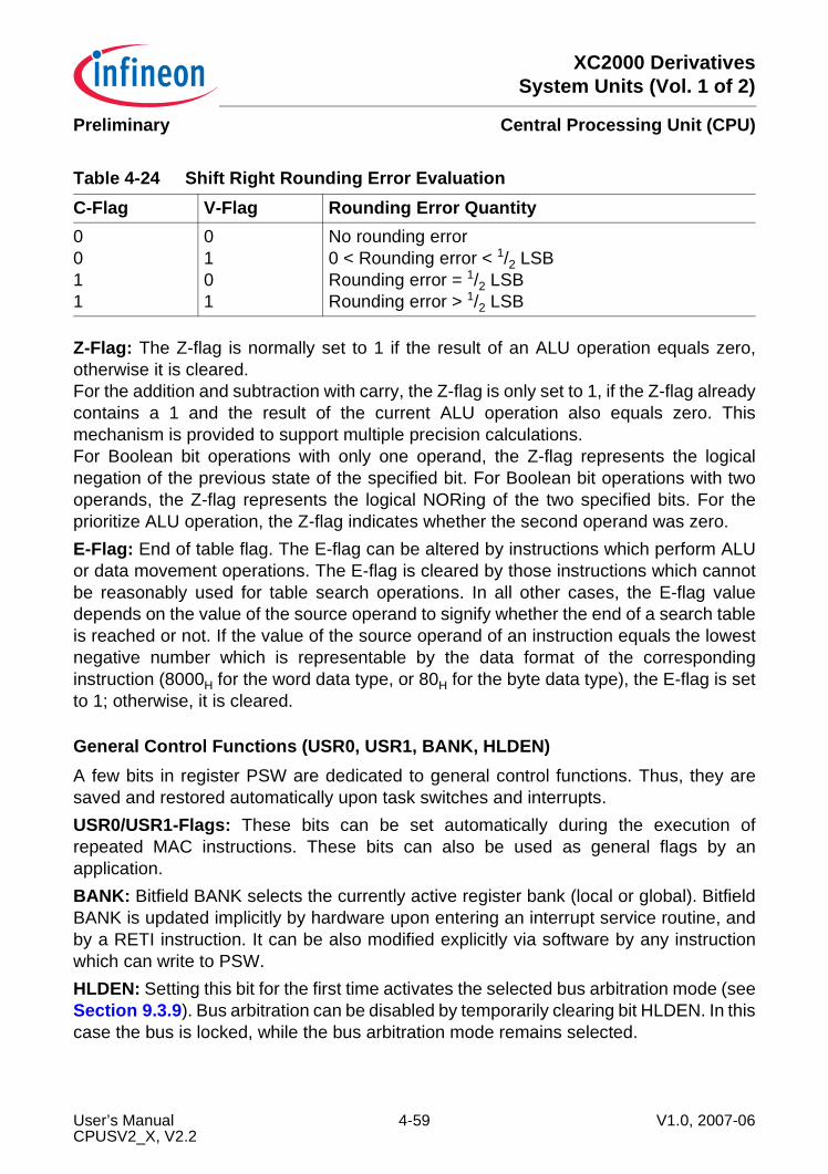
XC2000 DerivativesSystem Units (Vol. 1 of 2)
Central Processing Unit (CPU)Preliminary
Z-Flag: The Z-flag is normally set to 1 if the result of an ALU operation equals zero,otherwise it is cleared.For the addition and subtraction with carry, the Z-flag is only set to 1, if the Z-flag alreadycontains a 1 and the result of the current ALU operation also equals zero. Thismechanism is provided to support multiple precision calculations.For Boolean bit operations with only one operand, the Z-flag represents the logicalnegation of the previous state of the specified bit. For Boolean bit operations with twooperands, the Z-flag represents the logical NORing of the two specified bits. For theprioritize ALU operation, the Z-flag indicates whether the second operand was zero.E-Flag: End of table flag. The E-flag can be altered by instructions which perform ALUor data movement operations. The E-flag is cleared by those instructions which cannotbe reasonably used for table search operations. In all other cases, the E-flag valuedepends on the value of the source operand to signify whether the end of a search tableis reached or not. If the value of the source operand of an instruction equals the lowestnegative number which is representable by the data format of the correspondinginstruction (8000H for the word data type, or 80H for the byte data type), the E-flag is setto 1; otherwise, it is cleared.
General Control Functions (USR0, USR1, BANK, HLDEN)A few bits in register PSW are dedicated to general control functions. Thus, they aresaved and restored automatically upon task switches and interrupts.USR0/USR1-Flags: These bits can be set automatically during the execution ofrepeated MAC instructions. These bits can also be used as general flags by anapplication.BANK: Bitfield BANK selects the currently active register bank (local or global). BitfieldBANK is updated implicitly by hardware upon entering an interrupt service routine, andby a RETI instruction. It can be also modified explicitly via software by any instructionwhich can write to PSW.HLDEN: Setting this bit for the first time activates the selected bus arbitration mode (seeSection 9.3.9). Bus arbitration can be disabled by temporarily clearing bit HLDEN. In thiscase the bus is locked, while the bus arbitration mode remains selected.
Table 4-24 Shift Right Rounding Error EvaluationC-Flag V-Flag Rounding Error Quantity0011
0101
No rounding error0 < Rounding error < 1/2 LSBRounding error = 1/2 LSBRounding error > 1/2 LSB
User’s Manual 4-59 V1.0, 2007-06CPUSV2_X, V2.2
XC2000 DerivativesSystem Units (Vol. 1 of 2)
Central Processing Unit (CPU)Preliminary
CPU Interrupt Status (IEN, ILVL)IEN: The Interrupt Enable bit allows interrupts to be globally enabled (IEN = 1) ordisabled (IEN = 0).ILVL: The four-bit Interrupt Level field (ILVL) specifies the priority of the current CPUactivity. The interrupt level is updated by hardware on entry into an interrupt serviceroutine, but it can also be modified via software to prevent other interrupts from beingacknowledged. If an interrupt level 15 has been assigned to the CPU, it has the highestpossible priority; thus, the current CPU operation cannot be interrupted except byhardware traps or external non-maskable interrupts. For details refer to Chapter 5.After reset, all interrupts are globally disabled, and the lowest priority (ILVL = 0) isassigned to the initial CPU activity.
4.8.1 16-bit Adder/Subtracter, Barrel Shifter, and 16-bit Logic UnitAll standard arithmetic and logical operations are performed by the 16-bit ALU. In caseof byte operations, signals from bits 6 and 7 of the ALU result are used to control thecondition flags. Multiple precision arithmetic is supported by a “CARRY-IN” signal to theALU from previously calculated portions of the desired operation.A 16-bit barrel shifter provides multiple bit shifts in a single cycle. Rotations andarithmetic shifts are also supported.
4.8.2 Bit Manipulation UnitThe XC2000 offers a large number of instructions for bit processing. These instructionseither manipulate software flags within the internal RAM, control on-chip peripherals viacontrol bits in their respective SFRs, or control IO functions via port pins.Unlike other microcontrollers, the XC2000 features instructions that provide directaccess to two operands in the bit addressable space without requiring them to be movedto temporary locations. Multiple bit shift instructions have been included to avoid longinstruction streams of single bit shift operations. These instructions require a single CPUcycle.The instructions BSET, BCLR, BAND, BOR, BXOR, BMOV, BMOVN explicitly set orclear specific bits. The bitfield instructions BFLDL and BFLDH allow manipulation of upto 8 bits of a specific byte at one time. The instructions JBC and JNBS implicitly clear orset the specified bit when the jump is taken. The instructions JB and JNB (alsoconditional jump instructions that refer to flags) evaluate the specified bit to determine ifthe jump is to be taken.Note: Bit operations on undefined bit locations will always read a bit value of ‘0’, while
the write access will not affect the respective bit location.
All instructions that manipulate single bits or bit groups internally use a read-modify-writesequence that accesses the whole word containing the specified bit(s).
User’s Manual 4-60 V1.0, 2007-06CPUSV2_X, V2.2
XC2000 DerivativesSystem Units (Vol. 1 of 2)
Central Processing Unit (CPU)Preliminary
This method has several consequences:• The read-modify-write approach may be critical with hardware-affected bits. In these
cases, the hardware may change specific bits while the read-modify-write operationis in progress; thus, the writeback would overwrite the new bit value generated by thehardware. The solution is provided by either the implemented hardware protection(see below) or through special programming (see Section 4.3).
• Bits can be modified only within the internal address areas (internal RAM and SFRs).External locations cannot be used with bit instructions.
The upper 256 bytes of SFR area, ESFR area, and internal DPRAM are bit-addressable;so, the register bits located within those respective sections can be manipulated directlyusing bit instructions. The other SFRs must be accessed byte/word wise.Note: All GPRs are bit-addressable independently from the allocation of the register
bank via the Context Pointer (CP). Even GPRs which are allocated to non-bit-addressable RAM locations provide this feature.
Protected bits are not changed during the read-modify-write sequence, such as whenhardware sets an interrupt request flag between the read and the write of the read-modify-write sequence. The hardware protection logic guarantees that only the intendedbit(s) is/are affected by the write-back operation.Note: If a conflict occurs between a bit manipulation generated by hardware and an
intended software access, the software access has priority and determines thefinal value of the respective bit.
User’s Manual 4-61 V1.0, 2007-06CPUSV2_X, V2.2
XC2000 DerivativesSystem Units (Vol. 1 of 2)
Central Processing Unit (CPU)Preliminary
4.8.3 Multiply and Divide Unit The XC2000’s multiply and divide unit has two separated parts. One is the fast 16 ×16-bit multiplier that executes a multiplication in one CPU cycle. The other one is adivision sub-unit which performs the division algorithm in 18 … 21 CPU cycles(depending on the data and division types). The divide instruction requires four CPUcycles to be executed. For performance reasons, the rest of the division algorithm runsin the background during the following seventeen CPU cycles, while further instructionsare executed in parallel. Interrupt tasks can also be started and executed immediatelywithout any delay. If an instruction (from the original instruction stream or from theinterrupt task) tries to use the unit while a division is still running, the execution of thisnew instruction is stalled until the previous division is finished.To avoid these stalls, the multiply and division unit should not be used during the firstfourteen CPU cycles of the interrupt tasks. For example, this requires up to fourteen one-cycle instructions to be executed between the interrupt entry and the first instructionwhich uses the multiply and divide unit again (worst case).Multiplications and divisions implicitly use the 32-bit multiply/divide register MD(represented by the concatenation of the two non-bit-addressable data registers MDHand MDL) and the associated control register MDC. This bit-addressable 16-bit registeris implicitly used by the CPU when it performs a division or multiplication in the ALU.After a multiplication, MD represents the 32-bit result. For long divisions, MD must beloaded with the 32-bit dividend before the division is started. After any division, registerMDH represents the 16-bit remainder, register MDL represents the 16-bit quotient.
MDH Multiply/Divide High Reg. SFR (FE0CH/06H) Reset Value: 0000H
15 14 13 12 11 10 9 8 7 6 5 4 3 2 1 0
mdh
rwh
Field Bits Type Descriptionmdh [15:0] rwh High Part of MD
The high order sixteen bits of the 32-bit multiply and divide register MD.
User’s Manual 4-62 V1.0, 2007-06CPUSV2_X, V2.2
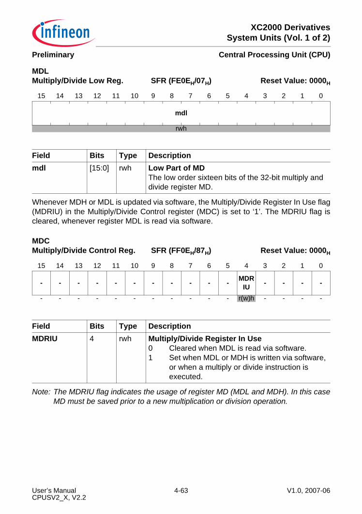
XC2000 DerivativesSystem Units (Vol. 1 of 2)
Central Processing Unit (CPU)Preliminary
Whenever MDH or MDL is updated via software, the Multiply/Divide Register In Use flag(MDRIU) in the Multiply/Divide Control register (MDC) is set to ‘1’. The MDRIU flag iscleared, whenever register MDL is read via software.
Note: The MDRIU flag indicates the usage of register MD (MDL and MDH). In this caseMD must be saved prior to a new multiplication or division operation.
MDL Multiply/Divide Low Reg. SFR (FE0EH/07H) Reset Value: 0000H
15 14 13 12 11 10 9 8 7 6 5 4 3 2 1 0
mdl
rwh
Field Bits Type Descriptionmdl [15:0] rwh Low Part of MD
The low order sixteen bits of the 32-bit multiply and divide register MD.
MDC Multiply/Divide Control Reg. SFR (FF0EH/87H) Reset Value: 0000H
15 14 13 12 11 10 9 8 7 6 5 4 3 2 1 0
- - - - - - - - - - - MDR IU - - - -
- - - - - - - - - - - r(w)h - - - -
Field Bits Type DescriptionMDRIU 4 rwh Multiply/Divide Register In Use
0 Cleared when MDL is read via software.1 Set when MDL or MDH is written via software,
or when a multiply or divide instruction is executed.
User’s Manual 4-63 V1.0, 2007-06CPUSV2_X, V2.2
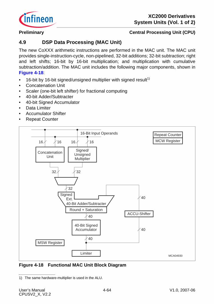
XC2000 DerivativesSystem Units (Vol. 1 of 2)
Central Processing Unit (CPU)Preliminary
4.9 DSP Data Processing (MAC Unit)The new CoXXX arithmetic instructions are performed in the MAC unit. The MAC unitprovides single-instruction-cycle, non-pipelined, 32-bit additions; 32-bit subtraction; rightand left shifts; 16-bit by 16-bit multiplication; and multiplication with cumulativesubtraction/addition. The MAC unit includes the following major components, shown inFigure 4-18:• 16-bit by 16-bit signed/unsigned multiplier with signed result1)
• Concatenation Unit• Scaler (one-bit left shifter) for fractional computing• 40-bit Adder/Subtracter• 40-bit Signed Accumulator• Data Limiter• Accumulator Shifter• Repeat Counter
Figure 4-18 Functional MAC Unit Block Diagram
1) The same hardware-multiplier is used in the ALU.
MCA04930
40-Bit Adder/Subtracter
SignedExt.
Round + Saturation
32
Signed/UnsignedMultiplier
ConcatenationUnit
3232
16 16 16 16
16-Bit Input Operands
40
40-Bit SignedAccumulator
Limiter
40
ACCU-Shifter
40
40
MSW Register
Repeat Counter
MCW Register
User’s Manual 4-64 V1.0, 2007-06CPUSV2_X, V2.2
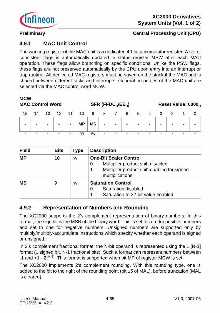
XC2000 DerivativesSystem Units (Vol. 1 of 2)
Central Processing Unit (CPU)Preliminary
4.9.1 MAC Unit ControlThe working register of the MAC unit is a dedicated 40-bit accumulator register. A set ofconsistent flags is automatically updated in status register MSW after each MACoperation. These flags allow branching on specific conditions. Unlike the PSW flags,these flags are not preserved automatically by the CPU upon entry into an interrupt ortrap routine. All dedicated MAC registers must be saved on the stack if the MAC unit isshared between different tasks and interrupts. General properties of the MAC unit areselected via the MAC control word MCW.
4.9.2 Representation of Numbers and RoundingThe XC2000 supports the 2’s complement representation of binary numbers. In thisformat, the sign bit is the MSB of the binary word. This is set to zero for positive numbersand set to one for negative numbers. Unsigned numbers are supported only bymultiply/multiply-accumulate instructions which specify whether each operand is signedor unsigned.In 2’s complement fractional format, the N-bit operand is represented using the 1.[N-1]format (1 signed bit, N-1 fractional bits). Such a format can represent numbers between-1 and +1 - 2-[N-1]. This format is supported when bit MP of register MCW is set.The XC2000 implements 2’s complement rounding. With this rounding type, one isadded to the bit to the right of the rounding point (bit 15 of MAL), before truncation (MALis cleared).
MCW MAC Control Word SFR (FFDCH/EEH) Reset Value: 0000H
15 14 13 12 11 10 9 8 7 6 5 4 3 2 1 0
- - - - - MP MS - - - - - - - - -
- - - - - rw rw - - - - - - - - -
Field Bits Type DescriptionMP 10 rw One-Bit Scaler Control
0 Multiplier product shift disabled1 Multiplier product shift enabled for signed
multiplicationsMS 9 rw Saturation Control
0 Saturation disabled1 Saturation to 32-bit value enabled
User’s Manual 4-65 V1.0, 2007-06CPUSV2_X, V2.2
XC2000 DerivativesSystem Units (Vol. 1 of 2)
Central Processing Unit (CPU)Preliminary
4.9.3 The 16-bit by 16-bit Signed/Unsigned Multiplier and ScalerThe multiplier executes 16-bit by 16-bit parallel signed/unsigned fractional and integermultiplication in one CPU-cycle. The multiplier allows the multiplication of unsigned andsigned operands. The result is always presented in a signed fractional or integer format.The result of the multiplication feeds a one-bit scaler to allow compensation for the extrasign bit gained in multiplying two 16-bit 2’s complement numbers.
4.9.4 Concatenation UnitThe concatenation unit enables the MAC unit to perform 32-bit arithmetic operations inone CPU cycle. The concatenation unit concatenates two 16-bit operands to a 32-bitoperand before the 32-bit arithmetic operation is executed in the 40-bit adder/subtracter.The second required operand is always the current accumulator contents. Theconcatenation unit is also used to pre-load the accumulator with a 32-bit value.
4.9.5 One-bit ScalerThe one-bit scaler can shift the result of the concatenation unit or the output of themultiplier one bit to the left. The scaler is controlled by the executed instruction for theconcatenation or by control bit MP in register MCW.If bit MP is set the product is shifted one bit to the left to compensate for the extra signbit gained in multiplying two 16-bit 2’s-complement numbers. The enabled automaticshift is performed only if both input operands are signed.
4.9.6 The 40-bit Adder/SubtracterThe 40-bit Adder/Subtracter allows intermediate overflows in a series ofmultiply/accumulate operations. The Adder/Subtracter has two input ports. The 40-bitport is the feedback of the accumulator output through the ACCU-Shifter to theAdder/Subtracter. The 32-bit port is the input port for the operand coming from the one-bit Scaler. The 32-bit operands are signed and extended to 40 bits before theaddition/subtraction is performed.The output of the Adder/Subtracter goes to the accumulator. It is also possible to roundthe result and to saturate it on a 32-bit value automatically after every accumulation. Theround operation is performed by adding 00’0000’8000H to the result. Automaticsaturation is enabled by setting the saturation control bit MS in register MCW.When the accumulator is in the overflow saturation mode and an overflow occurs, theaccumulator is loaded with either the most positive or the most negative valuerepresentable in a 32-bit value, depending on the direction of the overflow as well as onthe arithmetic used. The value of the accumulator upon saturation is either00’7FFF’FFFFH (positive) or FF’8000’0000H (negative).
User’s Manual 4-66 V1.0, 2007-06CPUSV2_X, V2.2
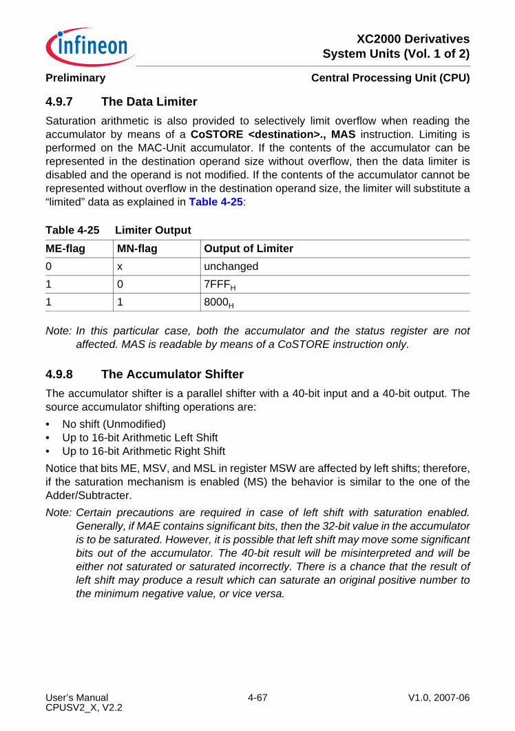
XC2000 DerivativesSystem Units (Vol. 1 of 2)
Central Processing Unit (CPU)Preliminary
4.9.7 The Data LimiterSaturation arithmetic is also provided to selectively limit overflow when reading theaccumulator by means of a CoSTORE <destination>., MAS instruction. Limiting isperformed on the MAC-Unit accumulator. If the contents of the accumulator can berepresented in the destination operand size without overflow, then the data limiter isdisabled and the operand is not modified. If the contents of the accumulator cannot berepresented without overflow in the destination operand size, the limiter will substitute a“limited” data as explained in Table 4-25:
Note: In this particular case, both the accumulator and the status register are notaffected. MAS is readable by means of a CoSTORE instruction only.
4.9.8 The Accumulator ShifterThe accumulator shifter is a parallel shifter with a 40-bit input and a 40-bit output. Thesource accumulator shifting operations are:• No shift (Unmodified)• Up to 16-bit Arithmetic Left Shift• Up to 16-bit Arithmetic Right ShiftNotice that bits ME, MSV, and MSL in register MSW are affected by left shifts; therefore,if the saturation mechanism is enabled (MS) the behavior is similar to the one of theAdder/Subtracter.Note: Certain precautions are required in case of left shift with saturation enabled.
Generally, if MAE contains significant bits, then the 32-bit value in the accumulatoris to be saturated. However, it is possible that left shift may move some significantbits out of the accumulator. The 40-bit result will be misinterpreted and will beeither not saturated or saturated incorrectly. There is a chance that the result ofleft shift may produce a result which can saturate an original positive number tothe minimum negative value, or vice versa.
Table 4-25 Limiter OutputME-flag MN-flag Output of Limiter0 x unchanged1 0 7FFFH
1 1 8000H
User’s Manual 4-67 V1.0, 2007-06CPUSV2_X, V2.2

XC2000 DerivativesSystem Units (Vol. 1 of 2)
Central Processing Unit (CPU)Preliminary
4.9.9 The 40-bit Signed Accumulator RegisterThe 40-bit accumulator consists of three concatenated registers MAE, MAH, and MAL.MAE is 8 bits wide, MAH and MAL are 16 bits wide. MAE is the Most Significant Byte ofthe 40-bit accumulator. This byte performs a guarding function. MAE is accessed as thelower byte of register MSW.When MAH is written, the value in the accumulator is automatically adjusted to signedextended 40-bit format. That means MAL is cleared and MAE will be automaticallyloaded with zeros for a positive number (the most significant bit of MAH is 0), and withones for a negative number (the most significant bit of MAH is 1), representing theextended 40-bit negative number in 2’s complement notation. One may see that theextended 40-bit value is equal to the 32-bit value without extension. In other words, afterthis extension, MAE does not contain significant bits. Generally, this condition is presentwhen the highest 9 bits of the 40-bit signed result are the same.During the accumulator operations, an overflow may happen and the result may not fitinto 32 bits and MAE will change. The extension flag “E” in register MSW is set when thesigned result in the accumulator has exceeded the 32-bit boundary. This condition ispresent when the highest 9 bits of the 40-bit signed result are not the same, i.e. MAEcontains significant bits.Most CoXXX operations specify the 40-bit accumulator register as a source and/or adestination operand.
MAL Accumulator Low Word SFR (FE5CH/2EH) Reset Value: 0000H
15 14 13 12 11 10 9 8 7 6 5 4 3 2 1 0
MAL
rwh
Field Bits Type DescriptionMAL [15:0] rwh Low Part of Accumulator
The 40-bit accumulator is completed by the accumulator high word (MAH) and bitfield MAE
User’s Manual 4-68 V1.0, 2007-06CPUSV2_X, V2.2
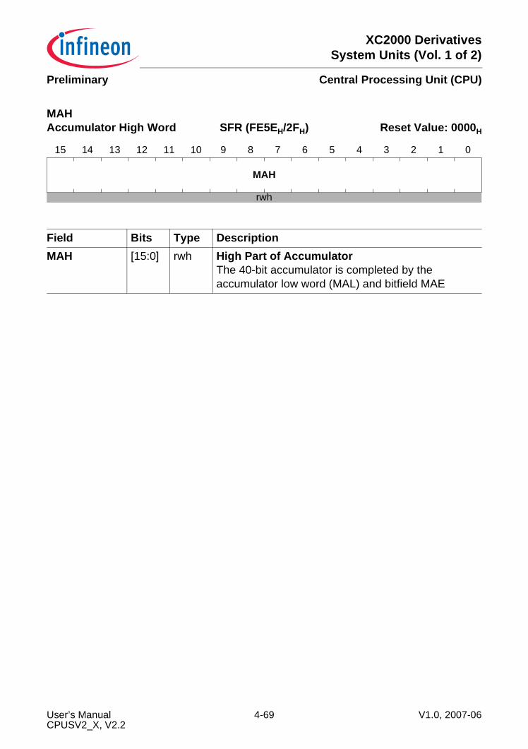
XC2000 DerivativesSystem Units (Vol. 1 of 2)
Central Processing Unit (CPU)Preliminary
MAH Accumulator High Word SFR (FE5EH/2FH) Reset Value: 0000H
15 14 13 12 11 10 9 8 7 6 5 4 3 2 1 0
MAH
rwh
Field Bits Type DescriptionMAH [15:0] rwh High Part of Accumulator
The 40-bit accumulator is completed by the accumulator low word (MAL) and bitfield MAE
User’s Manual 4-69 V1.0, 2007-06CPUSV2_X, V2.2
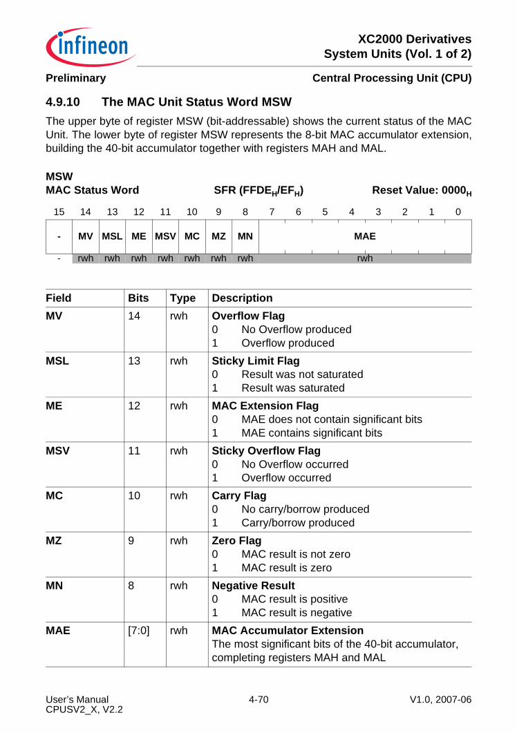
XC2000 DerivativesSystem Units (Vol. 1 of 2)
Central Processing Unit (CPU)Preliminary
4.9.10 The MAC Unit Status Word MSWThe upper byte of register MSW (bit-addressable) shows the current status of the MACUnit. The lower byte of register MSW represents the 8-bit MAC accumulator extension,building the 40-bit accumulator together with registers MAH and MAL.
MSW MAC Status Word SFR (FFDEH/EFH) Reset Value: 0000H
15 14 13 12 11 10 9 8 7 6 5 4 3 2 1 0
- MV MSL ME MSV MC MZ MN MAE
- rwh rwh rwh rwh rwh rwh rwh rwh
Field Bits Type DescriptionMV 14 rwh Overflow Flag
0 No Overflow produced1 Overflow produced
MSL 13 rwh Sticky Limit Flag0 Result was not saturated1 Result was saturated
ME 12 rwh MAC Extension Flag0 MAE does not contain significant bits1 MAE contains significant bits
MSV 11 rwh Sticky Overflow Flag0 No Overflow occurred1 Overflow occurred
MC 10 rwh Carry Flag0 No carry/borrow produced1 Carry/borrow produced
MZ 9 rwh Zero Flag0 MAC result is not zero1 MAC result is zero
MN 8 rwh Negative Result0 MAC result is positive1 MAC result is negative
MAE [7:0] rwh MAC Accumulator ExtensionThe most significant bits of the 40-bit accumulator, completing registers MAH and MAL
User’s Manual 4-70 V1.0, 2007-06CPUSV2_X, V2.2
XC2000 DerivativesSystem Units (Vol. 1 of 2)
Central Processing Unit (CPU)Preliminary
MAC Unit Status (MV, MN, MZ, MC, MSV, ME, MSL)These condition flags indicate the MAC status resulting from the most recentlyperformed MAC operation. These flags are controlled by the majority of MAC instructionsaccording to specific rules. Those rules depend on the instruction managing the MAC ordata movement operation.After execution of an instruction which explicitly updates register MSW, the conditionflags may no longer represent an actual MAC status. An explicit write operation toregister MSW supersedes the condition flag values implicitly generated by the MAC unit.An explicit read access returns the value of register MSW after execution of theimmediately preceding instruction. Register MSW can be accessed via any instructioncapable of accessing an SFR.Note: After reset, all MAC status bits are cleared.
MN-Flag: For the majority of the MAC operations, the MN-flag is set to 1 if the mostsignificant bit of the result contains a 1; otherwise, it is cleared. In the case of integeroperations, the MN-flag can be interpreted as the sign bit of the result (negative: MN = 1,positive: MN = 0). Negative numbers are always represented as the 2’s complement ofthe corresponding positive number. The range of signed numbers extends from80’0000’0000H to 7F’FFFF’FFFFH.MZ-Flag: The MZ-flag is normally set to 1 if the result of a MAC operation equals zero;otherwise, it is cleared.MC-Flag: After a MAC addition, the MC-flag indicates that a “Carry” from the mostsignificant bit of the accumulator extension MAE has been generated. After a MACsubtraction or a MAC comparison, the MC-flag indicates a “Borrow” representing thelogical negation of a “Carry” for the addition. This means that the MC-flag is set to 1 if no“Carry” from the most significant bit of the accumulator has been generated during asubtraction. Subtraction is performed by the MAC Unit as a 2’s complement addition andthe MC-flag is cleared when this complement addition caused a “Carry”.For left-shift MAC operations, the MC-flag represents the value of the bit shifted out last.Right-shift MAC operations always clear the MC-flag. The arithmetic right-shift MACoperation can set the MC-flag if the enabled round operation generates a “Carry” fromthe most significant bit of the accumulator extension MAE.MSV-Flag: The addition, subtraction, 2’s complement, and round operations always setthe MSV-flag to 1 if the MAC result exceeds the maximum range of 40-bit signednumbers. If the MSV-flag indicates an arithmetic overflow, the MAC result of anoperation is not valid.The MSV-flag is a ‘Sticky Bit’. Once set, other MAC operations cannot affect the statusof the MSV-flag. Only a direct write operation can clear the MSV-flag.ME-Flag: The ME-flag is set if the accumulator extension MAE contains significant bits,that means if the nine highest accumulator bits are not all equal.
User’s Manual 4-71 V1.0, 2007-06CPUSV2_X, V2.2
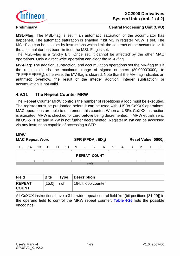
XC2000 DerivativesSystem Units (Vol. 1 of 2)
Central Processing Unit (CPU)Preliminary
MSL-Flag: The MSL-flag is set if an automatic saturation of the accumulator hashappened. The automatic saturation is enabled if bit MS in register MCW is set. TheMSL-Flag can be also set by instructions which limit the contents of the accumulator. Ifthe accumulator has been limited, the MSL-Flag is set.The MSL-Flag is a ‘Sticky Bit’. Once set, it cannot be affected by the other MACoperations. Only a direct write operation can clear the MSL-flag.MV-Flag: The addition, subtraction, and accumulation operations set the MV-flag to 1 ifthe result exceeds the maximum range of signed numbers (80’0000’0000H to7F’FFFF’FFFFH); otherwise, the MV-flag is cleared. Note that if the MV-flag indicates anarithmetic overflow, the result of the integer addition, integer subtraction, oraccumulation is not valid.
4.9.11 The Repeat Counter MRWThe Repeat Counter MRW controls the number of repetitions a loop must be executed.The register must be pre-loaded before it can be used with -USRx CoXXX operations.MAC operations are able to decrement this counter. When a -USRx CoXXX instructionis executed, MRW is checked for zero before being decremented. If MRW equals zero,bit USRx is set and MRW is not further decremented. Register MRW can be accessedvia any instruction capable of accessing a SFR.
All CoXXX instructions have a 3-bit wide repeat control field ‘rrr’ (bit positions [31:29]) inthe operand field to control the MRW repeat counter. Table 4-26 lists the possibleencodings.
MRW MAC Repeat Word SFR (FFDAH/EDH) Reset Value: 0000H
15 14 13 12 11 10 9 8 7 6 5 4 3 2 1 0
REPEAT_COUNT
rwh
Field Bits Type DescriptionREPEAT_ COUNT
[15:0] rwh 16-bit loop counter
User’s Manual 4-72 V1.0, 2007-06CPUSV2_X, V2.2
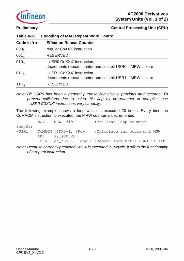
XC2000 DerivativesSystem Units (Vol. 1 of 2)
Central Processing Unit (CPU)Preliminary
Note: Bit USR0 has been a general purpose flag also in previous architectures. Toprevent collisions due to using this flag by programmer or compiler, use‘-USR0 C0XXX’ instructions very carefully.
The following example shows a loop which is executed 20 times. Every time theCoMACM instruction is executed, the MRW counter is decremented. MOV MRW, #19 ;Pre-load loop counterloop01:-USR1 CoMACM [IDX0+], [R0+] ;Calculate and decrement MSW ADD R2,#0002H JMPA cc_nusr1, loop01 ;Repeat loop until USR1 is set
Note: Because correctly predicted JMPA is executed in 0-cycle, it offers the functionalityof a repeat instruction.
Table 4-26 Encoding of MAC Repeat Word ControlCode in ‘rrr’ Effect on Repeat Counter000B regular CoXXX instruction001B RESERVED010B ‘-USR0 CoXXX’ instruction,
decrements repeat counter and sets bit USR0 if MRW is zero011B ‘-USR1 CoXXX’ instruction,
decrements repeat counter and sets bit USR1 if MRW is zero1XXB RESERVED
User’s Manual 4-73 V1.0, 2007-06CPUSV2_X, V2.2
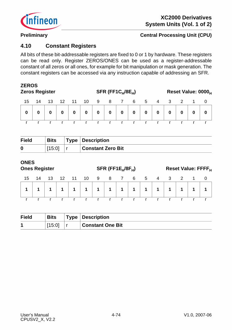
XC2000 DerivativesSystem Units (Vol. 1 of 2)
Central Processing Unit (CPU)Preliminary
4.10 Constant RegistersAll bits of these bit-addressable registers are fixed to 0 or 1 by hardware. These registerscan be read only. Register ZEROS/ONES can be used as a register-addressableconstant of all zeros or all ones, for example for bit manipulation or mask generation. Theconstant registers can be accessed via any instruction capable of addressing an SFR.
ZEROS Zeros Register SFR (FF1CH/8EH) Reset Value: 0000H
15 14 13 12 11 10 9 8 7 6 5 4 3 2 1 0
0 0 0 0 0 0 0 0 0 0 0 0 0 0 0 0
r r r r r r r r r r r r r r r r
Field Bits Type Description0 [15:0] r Constant Zero Bit
ONES Ones Register SFR (FF1EH/8FH) Reset Value: FFFFH
15 14 13 12 11 10 9 8 7 6 5 4 3 2 1 0
1 1 1 1 1 1 1 1 1 1 1 1 1 1 1 1
r r r r r r r r r r r r r r r r
Field Bits Type Description1 [15:0] r Constant One Bit
User’s Manual 4-74 V1.0, 2007-06CPUSV2_X, V2.2
XC2000 DerivativesSystem Units (Vol. 1 of 2)
Interrupt and Trap FunctionsPreliminary
5 Interrupt and Trap FunctionsThe architecture of the XC2000 supports several mechanisms for fast and flexibleresponse to service requests from various sources internal or external to themicrocontroller. Different kinds of exceptions are handled in a similar way:• Interrupts generated by the Interrupt Controller (ITC)• DMA transfers issued by the Peripheral Event Controller (PEC)• Traps caused by the TRAP instruction or issued by faults or specific system states
Normal Interrupt ProcessingThe CPU temporarily suspends current program execution and branches to an interruptservice routine to service an interrupt requesting device. The current program status (IP,PSW, also CSP in segmentation mode) is saved on the internal system stack. Aprioritization scheme with 16 priority levels allows the user to specify the order in whichmultiple interrupt requests are to be handled.
Interrupt Processing via the Peripheral Event Controller (PEC)A faster alternative to normal software controlled interrupt processing is servicing aninterrupt requesting device with the XC2000’s integrated Peripheral Event Controller(PEC). Triggered by an interrupt request, the PEC performs a single word or byte datatransfer between any two locations through one of eight programmable PEC ServiceChannels. During a PEC transfer, normal program execution of the CPU is halted. Nointernal program status information needs to be saved. The same prioritization schemeis used for PEC service as for normal interrupt processing.
Trap FunctionsTrap functions are activated in response to special conditions that occur during theexecution of instructions. A trap can also be caused externally via the External ServiceRequest pins, ESRx. Several hardware trap functions are provided to handle erroneousconditions and exceptions arising during instruction execution. Hardware traps alwayshave highest priority and cause immediate system reaction. The software trap functionis invoked by the TRAP instruction that generates a software interrupt for a specifiedinterrupt vector. For all types of traps, the current program status is saved on the systemstack.
External Interrupt ProcessingAlthough the XC2000 does not provide dedicated interrupt pins, it allows connection ofexternal interrupt sources and provides several mechanisms to react to external eventsincluding standard inputs, non-maskable interrupts, and fast external interrupts. Exceptfor the non-maskable interrupt and the reset input, these interrupt functions are alternateport functions.
User’s Manual 5-1 V1.0, 2007-06ICU_X2K, V2.2
XC2000 DerivativesSystem Units (Vol. 1 of 2)
Interrupt and Trap FunctionsPreliminary
5.1 Interrupt System StructureThe XC2000 provides 96 separate interrupt nodes assignable to 16 priority levels, with8 sub-levels (group priority) on each level. In order to support modular and consistentsoftware design techniques, most sources of an interrupt or PEC request are suppliedwith a separate interrupt control register and an interrupt vector. The control registercontains the interrupt request flag, the interrupt enable bit, and the interrupt priority of theassociated source. Each source request is then activated by one specific event,determined by the selected operating mode of the respective device. For efficientresource usage, multi-source interrupt nodes are also incorporated. These nodes can beactivated by several source requests, such as by different kinds of errors in the serialinterfaces. However, specific status flags which identify the type of error areimplemented in the serial channels’ control registers. Additional sharing of interruptnodes is supported via interrupt subnode control registers.The XC2000 provides a vectored interrupt system. In this system specific vectorlocations in the memory space are reserved for the reset, trap, and interrupt servicefunctions. Whenever a request occurs, the CPU branches to the location that isassociated with the respective interrupt source. This allows direct identification of thesource which caused the request. The Class B hardware traps all share the sameinterrupt vector. The status flags in the Trap Flag Register (TFR) can then be used todetermine which exception caused the trap. For the special software TRAP instruction,the vector address is specified by the operand field of the instruction, which is a sevenbit trap number.The reserved vector locations build a jump table in the low end of a segment (selectedby register VECSEG) in the XC2000’s address space. The jump table consists of theappropriate jump instructions which transfer control to the interrupt or trap serviceroutines and which may be located anywhere within the address space. The entries ofthe jump table are located at the lowest addresses in the selected code segment. Eachentry occupies 2, 4, 8, or 16 words (selected by bitfield VECSC in register CPUCON1),providing room for at least one doubleword instruction. The respective vector locationresults from multiplying the trap number by the selected step width (2(VECSC+2)).All pending interrupt requests are arbitrated. The arbitration winner is indicated to theCPU together with its priority level and action request. The CPU triggers thecorresponding action based on the required functionality (normal interrupt, PEC, jumptable cache, etc.) of the arbitration winner.An action request will be accepted by the CPU if the requesting source has a higherpriority than the current CPU priority level and interrupts are globally enabled. If therequesting source has a lower (or equal) interrupt level priority than the current CPUtask, it remains pending.
User’s Manual 5-2 V1.0, 2007-06ICU_X2K, V2.2
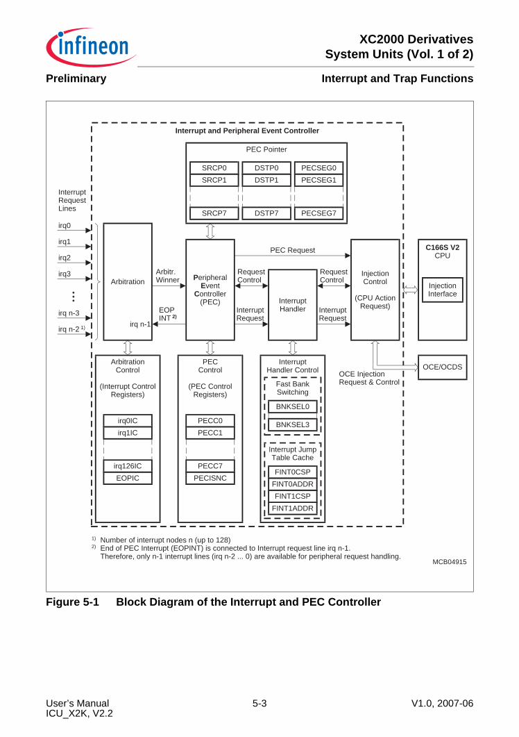
XC2000 DerivativesSystem Units (Vol. 1 of 2)
Interrupt and Trap FunctionsPreliminary
Figure 5-1 Block Diagram of the Interrupt and PEC Controller
MCB04915
FINT1ADDR
FINT1CSP
FINT0ADDR
FINT0CSP
Interrupt JumpTable Cache
BNKSEL3
BNKSEL0
Fast BankSwitching
InterruptHandler Control
PECC1
PECC0
PECControl
(PEC ControlRegisters)
PECISNC
PECC7
irq1IC
irq0IC
ArbitrationControl
(Interrupt ControlRegisters)
EOPIC
irq126IC
PeripheralEvent
Controller(PEC)
Arbitration
InterruptHandlerInterrupt
Request
RequestControl
EOPINT 2)
Arbitr.Winner
InterruptRequest
RequestControl
InjectionControl
(CPU ActionRequest)
PEC Request
irq n-1
SRCP1
SRCP0
SRCP7
DSTP1
DSTP0
DSTP7
PECSEG1
PECSEG0
PECSEG7
PEC Pointer
Interrupt and Peripheral Event Controller
irq n-2 1)
irq n-3
irq0
irq1
irq2
irq3
InterruptRequestLines
C166S V2CPU
InjectionInterface
OCE/OCDSOCE InjectionRequest & Control
1) Number of interrupt nodes n (up to 128)2) End of PEC Interrupt (EOPINT) is connected to Interrupt request line irq n-1.
Therefore, only n-1 interrupt lines (irq n-2 ... 0) are available for peripheral request handling.
User’s Manual 5-3 V1.0, 2007-06ICU_X2K, V2.2
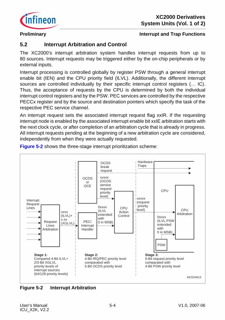
XC2000 DerivativesSystem Units (Vol. 1 of 2)
Interrupt and Trap FunctionsPreliminary
5.2 Interrupt Arbitration and ControlThe XC2000’s interrupt arbitration system handles interrupt requests from up to80 sources. Interrupt requests may be triggered either by the on-chip peripherals or byexternal inputs.Interrupt processing is controlled globally by register PSW through a general interruptenable bit (IEN) and the CPU priority field (ILVL). Additionally, the different interruptsources are controlled individually by their specific interrupt control registers (… IC).Thus, the acceptance of requests by the CPU is determined by both the individualinterrupt control registers and by the PSW. PEC services are controlled by the respectivePECCx register and by the source and destination pointers which specify the task of therespective PEC service channel.An interrupt request sets the associated interrupt request flag xxIR. If the requestinginterrupt node is enabled by the associated interrupt enable bit xxIE arbitration starts withthe next clock cycle, or after completion of an arbitration cycle that is already in progress.All interrupt requests pending at the beginning of a new arbitration cycle are considered,independently from when they were actually requested.Figure 5-2 shows the three-stage interrupt prioritization scheme:
Figure 5-2 Interrupt Arbitration
MCD04913
OCDSor
OCE
CPUArbitration
PEC/InterruptHandler
CPUActionControl
0xxxx(ILVLextendedwith0 in MSB)
xxxxx(OCDSservicerequestprioritylevel)
OCDSbreakrequest
xxxxx(request prioritylevel)
PSW
0xxxx(ILVL.PSWextendedwith0 in MSB)
RequestLines
Arbitration
xxxx(ILVL)+x.xx(XGLVL)
InterruptRequestLines
HardwareTraps
CPU
Stage 1:Compared 4-Bit ILVL+2/3-Bit XGLVLpriority levels ofinterrupt sources(64/128 priority levels)
Stage 2:4-Bit IRQ/PEC priority levelcomparated with5-Bit OCDS priority level
Stage 3:5-Bit request priority levelcomparated with4-Bit PSW priority level
User’s Manual 5-4 V1.0, 2007-06ICU_X2K, V2.2
XC2000 DerivativesSystem Units (Vol. 1 of 2)
Interrupt and Trap FunctionsPreliminary
The interrupt prioritization is done in three stages:• Select one of the active interrupt requests• Compare the priority levels of the selected request and an OCDS service request• Compare the priority level of the final request with the CPU priority level
The First Arbitration Stagecompares the priority levels of the active interrupt request lines. The interrupt prioritylevel of each requestor is defined by bitfield ILVL in the respective xxIC register. Theextended group priority level XGLVL (combined from bitfields GPX and GLVL) definesup to eight sub-priorities within one interrupt level. The group priority level distinguishesinterrupt requests assigned to the same priority level, so one winner can be determined.Note: All interrupt request sources that are enabled and programmed to the same
interrupt priority level (ILVL) must have different group priority levels. Otherwise,an incorrect interrupt vector will be generated.
The Second Arbitration Stagecompares the priority of the first stage winner with the priority of OCDS service requests.OCDS service requests bypass the first stage of arbitration and go directly to the CPUAction Control Unit. The CPU Action Control Unit compares the winner’s 4-bit prioritylevel (disregarding the group level) with the 5-bit OCDS service request priority. The 4-bitILVL of the interrupt request is extended to a 5-bit value with MSB = 0. This means thatany OCDS request with MSB = 1 will always win the second stage arbitration. However,if there is a conflict between an OCDS request and an interrupt request, the interruptrequest wins.
The Third Arbitration Stagecompares the priority level of the second stage winner with the priority of the current CPUtask. An action request will be accepted by the CPU only if the priority level of the requestis higher than the current CPU priority level (bitfield ILVL in register PSW) and if interruptand PEC requests are globally enabled by the global interrupt enable flag IEN in registerPSW. To compare with the 5-bit priority level of the second stage winner, the 4-bit CPUpriority level is extended to a 5-bit value with MSB = 0. This means that any request withMSB = 1 will always interrupt the current CPU task. If the requestor has a priority levellower than or equal to the current CPU task, the request remains pending.Note: Priority level 0000B is the default level of the CPU. Therefore, a request on
interrupt priority level 0000B will be arbitrated, but the CPU will never accept anaction request on this level. However, every individually enabled interrupt request(including all denied interrupt requests and priority level 0000B requests) triggersa CPU wake-up from idle state independent of the global interrupt enable bit IEN.
User’s Manual 5-5 V1.0, 2007-06ICU_X2K, V2.2
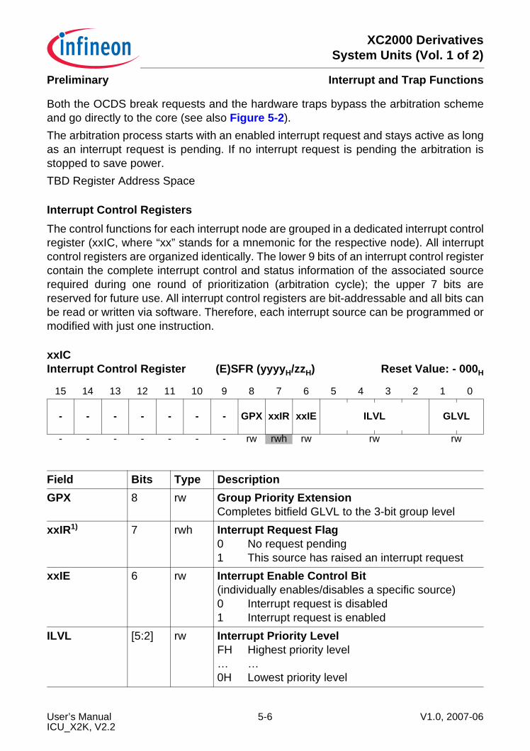
XC2000 DerivativesSystem Units (Vol. 1 of 2)
Interrupt and Trap FunctionsPreliminary
Both the OCDS break requests and the hardware traps bypass the arbitration schemeand go directly to the core (see also Figure 5-2).The arbitration process starts with an enabled interrupt request and stays active as longas an interrupt request is pending. If no interrupt request is pending the arbitration isstopped to save power.TBD Register Address Space
Interrupt Control RegistersThe control functions for each interrupt node are grouped in a dedicated interrupt controlregister (xxIC, where “xx” stands for a mnemonic for the respective node). All interruptcontrol registers are organized identically. The lower 9 bits of an interrupt control registercontain the complete interrupt control and status information of the associated sourcerequired during one round of prioritization (arbitration cycle); the upper 7 bits arereserved for future use. All interrupt control registers are bit-addressable and all bits canbe read or written via software. Therefore, each interrupt source can be programmed ormodified with just one instruction.
xxIC Interrupt Control Register (E)SFR (yyyyH/zzH) Reset Value: - 000H
15 14 13 12 11 10 9 8 7 6 5 4 3 2 1 0
- - - - - - - GPX xxIR xxIE ILVL GLVL
- - - - - - - rw rwh rw rw rw
Field Bits Type DescriptionGPX 8 rw Group Priority Extension
Completes bitfield GLVL to the 3-bit group levelxxIR1) 7 rwh Interrupt Request Flag
0 No request pending1 This source has raised an interrupt request
xxIE 6 rw Interrupt Enable Control Bit(individually enables/disables a specific source)0 Interrupt request is disabled1 Interrupt request is enabled
ILVL [5:2] rw Interrupt Priority LevelFH Highest priority level… …0H Lowest priority level
User’s Manual 5-6 V1.0, 2007-06ICU_X2K, V2.2
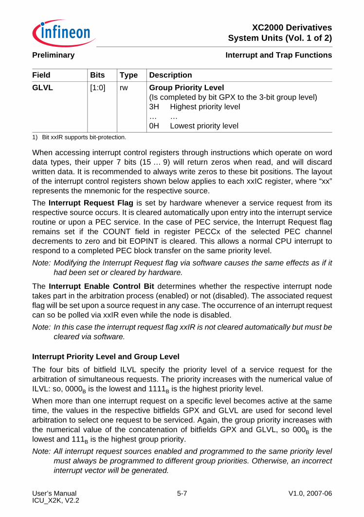
XC2000 DerivativesSystem Units (Vol. 1 of 2)
Interrupt and Trap FunctionsPreliminary
When accessing interrupt control registers through instructions which operate on worddata types, their upper 7 bits (15 … 9) will return zeros when read, and will discardwritten data. It is recommended to always write zeros to these bit positions. The layoutof the interrupt control registers shown below applies to each xxIC register, where “xx”represents the mnemonic for the respective source.The Interrupt Request Flag is set by hardware whenever a service request from itsrespective source occurs. It is cleared automatically upon entry into the interrupt serviceroutine or upon a PEC service. In the case of PEC service, the Interrupt Request flagremains set if the COUNT field in register PECCx of the selected PEC channeldecrements to zero and bit EOPINT is cleared. This allows a normal CPU interrupt torespond to a completed PEC block transfer on the same priority level.Note: Modifying the Interrupt Request flag via software causes the same effects as if it
had been set or cleared by hardware.
The Interrupt Enable Control Bit determines whether the respective interrupt nodetakes part in the arbitration process (enabled) or not (disabled). The associated requestflag will be set upon a source request in any case. The occurrence of an interrupt requestcan so be polled via xxIR even while the node is disabled.Note: In this case the interrupt request flag xxIR is not cleared automatically but must be
cleared via software.
Interrupt Priority Level and Group Level The four bits of bitfield ILVL specify the priority level of a service request for thearbitration of simultaneous requests. The priority increases with the numerical value ofILVL: so, 0000B is the lowest and 1111B is the highest priority level.When more than one interrupt request on a specific level becomes active at the sametime, the values in the respective bitfields GPX and GLVL are used for second levelarbitration to select one request to be serviced. Again, the group priority increases withthe numerical value of the concatenation of bitfields GPX and GLVL, so 000B is thelowest and 111B is the highest group priority.Note: All interrupt request sources enabled and programmed to the same priority level
must always be programmed to different group priorities. Otherwise, an incorrectinterrupt vector will be generated.
GLVL [1:0] rw Group Priority Level(Is completed by bit GPX to the 3-bit group level)3H Highest priority level… …0H Lowest priority level
1) Bit xxIR supports bit-protection.
Field Bits Type Description
User’s Manual 5-7 V1.0, 2007-06ICU_X2K, V2.2
XC2000 DerivativesSystem Units (Vol. 1 of 2)
Interrupt and Trap FunctionsPreliminary
Upon entry into the interrupt service routine, the priority level of the source that won thearbitration and whose priority level is higher than the current CPU level, is copied intobitfield ILVL of register PSW after pushing the old PSW contents onto the stack.The interrupt system of the XC2000 allows nesting of up to 15 interrupt service routinesof different priority levels (level 0 cannot be arbitrated).Interrupt requests programmed to priority levels 15 … 8 (i.e., ILVL = 1XXXB) can beserviced by the PEC if the associated PEC channel is properly assigned and enabled(please refer to Section 5.4). Interrupt requests programmed to priority levels 7 through1 will always be serviced by normal interrupt processing.Note: Priority level 0000B is the default level of the CPU. Therefore, a request on level 0
will never be serviced because it can never interrupt the CPU. However, anindividually enabled interrupt request (independent of bit IEN) on level 0000B willterminate the XC2000’s Idle mode and reactivate the CPU.
General Interrupt Control Functions in Register PSWThe acceptance of an interrupt request depends on the current CPU priority level (bitfieldILVL in register PSW) and the global interrupt enable control bit IEN in register PSW (seeSection 4.8).CPU Priority ILVL defines the current level for the operation of the CPU. This bitfieldreflects the priority level of the routine currently executed. Upon entry into an interruptservice routine, this bitfield is updated with the priority level of the request being serviced.The PSW is saved on the system stack before the request is serviced. The CPU leveldetermines the minimum interrupt priority level which will be serviced. Any request onthe same or a lower level will not be acknowledged. The current CPU priority level maybe adjusted via software to control which interrupt request sources will beacknowledged. PEC transfers do not really interrupt the CPU, but rather “steal” a singlecycle, so PEC services do not influence the ILVL field in the PSW.Hardware traps switch the CPU level to maximum priority (i.e. 15) so no interrupt or PECrequests will be acknowledged while an exception trap service routine is executed.Note: The TRAP instruction does not change the CPU level, so software invoked trap
service routines may be interrupted by higher requests.
Interrupt Enable bit IEN globally enables or disables PEC operation and theacceptance of interrupts by the CPU. When IEN is cleared, no new interrupt requests areaccepted by the CPU (see also Section 4.3.4). When IEN is set to 1, all interruptsources, which have been individually enabled by the interrupt enable bits in theirassociated control registers, are globally enabled. Traps are non-maskable and are,therefore, not affected by the IEN bit.Note: To generate requests, interrupt sources must be also enabled by the interrupt
enable bits in their associated control register.
User’s Manual 5-8 V1.0, 2007-06ICU_X2K, V2.2
XC2000 DerivativesSystem Units (Vol. 1 of 2)
Interrupt and Trap FunctionsPreliminary
Register Bank Select bitfield BANK defines the currently used register bank for theCPU operation. When the CPU enters an interrupt service routine, this bitfield is updatedto select the register bank associated with the serviced request:• Requests on priority levels 15 … 12 use the register bank pre-selected via the
respective bitfield GPRSELx in the corresponding BNKSEL register• Requests on priority levels 11 … 1 always use the global register bank,
i.e. BANK = 00B• Hardware traps always use the global register bank, i.e. BANK = 00B• The TRAP instruction does not change the current register bank
User’s Manual 5-9 V1.0, 2007-06ICU_X2K, V2.2
XC2000 DerivativesSystem Units (Vol. 1 of 2)
Interrupt and Trap FunctionsPreliminary
5.3 Interrupt Vector Table The XC2000 provides a vectored interrupt system. This system reserves a set of specificmemory locations, which are accessed automatically upon the respective trigger event.Entries for the following events are provided:• Reset (hardware, software, watchdog)• Traps (hardware-generated by fault conditions or via TRAP instruction)• Interrupt service requestsWhenever a request is accepted, the CPU branches to the location associated with therespective trigger source. This vector position directly identifies the source causing therequest, with two exceptions:• Class B hardware traps all share the same interrupt vector. The status flags in the
Trap Flag Register (TFR) are used to determine which exception caused the trap. Fordetails, see Section 5.11.
• An interrupt node may be shared by several interrupt requests, e.g. within a module.Additional flags identify the requesting source, so the software can handle eachrequest individually. For details, see Section 5.7.
The reserved vector locations build a vector table located in the address space of theXC2000. The vector table usually contains the appropriate jump instructions that transfercontrol to the interrupt or trap service routines. These routines may be located anywherewithin the address space. The location and organization of the vector table isprogrammable.The Vector Segment register VECSEG defines the segment of the Vector Table (can belocated in all segments, except for reserved areas).Bitfield VECSC in register CPUCON1 defines the space between two adjacent vectors(can be 2, 4, 8, or 16 words). For a summary of register CPUCON1, please refer toSection 4.4.Each vector location has an offset address to the segment base address of the vectortable (given by VECSEG). The offset can be easily calculated by multiplying the vectornumber with the vector space programmed in bitfield VECSC.Table 5-2 lists all sources capable of requesting interrupt or PEC service in the XC2000,the associated interrupt vector locations, the associated vector numbers, and theassociated interrupt control registers.Note: All interrupt nodes which are currently not used by their associated modules or are
not connected to a module in the actual derivative may be used to generatesoftware controlled interrupt requests by setting the respective IR flag.
User’s Manual 5-10 V1.0, 2007-06ICU_X2K, V2.2
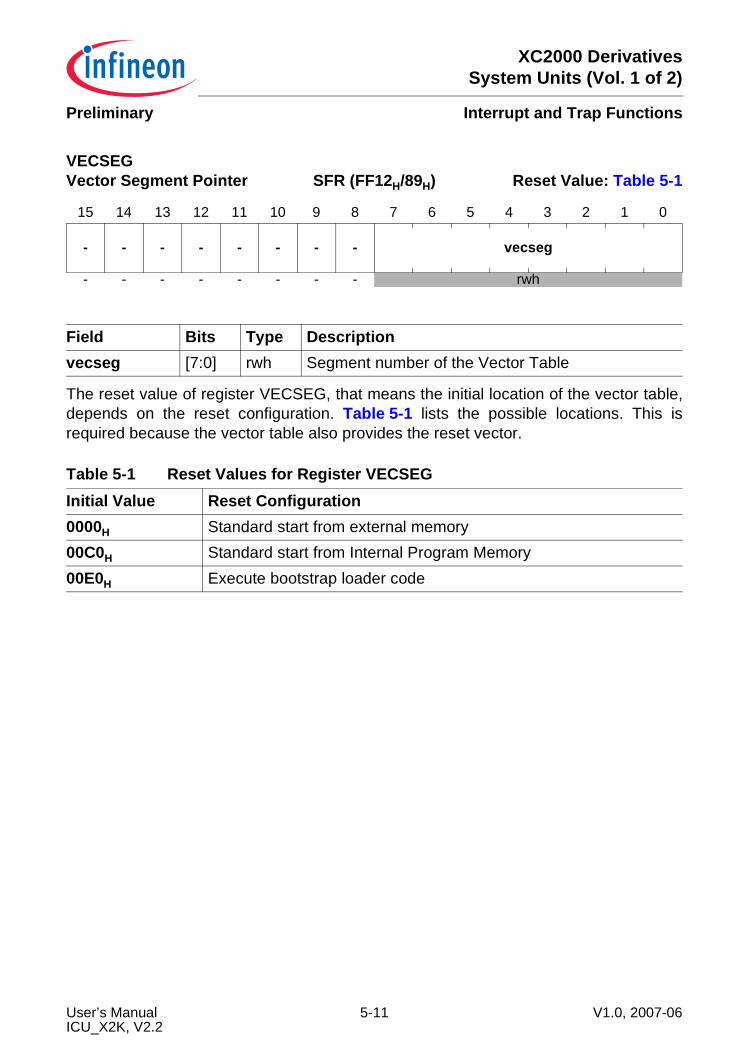
XC2000 DerivativesSystem Units (Vol. 1 of 2)
Interrupt and Trap FunctionsPreliminary
The reset value of register VECSEG, that means the initial location of the vector table,depends on the reset configuration. Table 5-1 lists the possible locations. This isrequired because the vector table also provides the reset vector.
VECSEG Vector Segment Pointer SFR (FF12H/89H) Reset Value: Table 5-1
15 14 13 12 11 10 9 8 7 6 5 4 3 2 1 0
- - - - - - - - vecseg
- - - - - - - - rwh
Field Bits Type Descriptionvecseg [7:0] rwh Segment number of the Vector Table
Table 5-1 Reset Values for Register VECSEGInitial Value Reset Configuration0000H Standard start from external memory00C0H Standard start from Internal Program Memory00E0H Execute bootstrap loader code
User’s Manual 5-11 V1.0, 2007-06ICU_X2K, V2.2
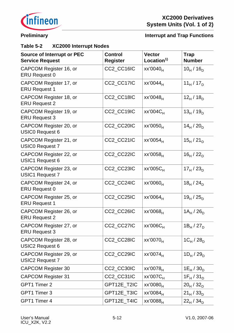
XC2000 DerivativesSystem Units (Vol. 1 of 2)
Interrupt and Trap FunctionsPreliminary
Table 5-2 XC2000 Interrupt NodesSource of Interrupt or PEC Service Request
Control Register
Vector Location1)
Trap Number
CAPCOM Register 16, orERU Request 0
CC2_CC16IC xx’0040H 10H / 16D
CAPCOM Register 17, orERU Request 1
CC2_CC17IC xx’0044H 11H / 17D
CAPCOM Register 18, orERU Request 2
CC2_CC18IC xx’0048H 12H / 18D
CAPCOM Register 19, orERU Request 3
CC2_CC19IC xx’004CH 13H / 19D
CAPCOM Register 20, orUSIC0 Request 6
CC2_CC20IC xx’0050H 14H / 20D
CAPCOM Register 21, orUSIC0 Request 7
CC2_CC21IC xx’0054H 15H / 21D
CAPCOM Register 22, orUSIC1 Request 6
CC2_CC22IC xx’0058H 16H / 22D
CAPCOM Register 23, orUSIC1 Request 7
CC2_CC23IC xx’005CH 17H / 23D
CAPCOM Register 24, orERU Request 0
CC2_CC24IC xx’0060H 18H / 24D
CAPCOM Register 25, orERU Request 1
CC2_CC25IC xx’0064H 19H / 25D
CAPCOM Register 26, orERU Request 2
CC2_CC26IC xx’0068H 1AH / 26D
CAPCOM Register 27, orERU Request 3
CC2_CC27IC xx’006CH 1BH / 27D
CAPCOM Register 28, orUSIC2 Request 6
CC2_CC28IC xx’0070H 1CH / 28D
CAPCOM Register 29, orUSIC2 Request 7
CC2_CC29IC xx’0074H 1DH / 29D
CAPCOM Register 30 CC2_CC30IC xx’0078H 1EH / 30D
CAPCOM Register 31 CC2_CC31IC xx’007CH 1FH / 31D
GPT1 Timer 2 GPT12E_T2IC xx’0080H 20H / 32D
GPT1 Timer 3 GPT12E_T3IC xx’0084H 21H / 33D
GPT1 Timer 4 GPT12E_T4IC xx’0088H 22H / 34D
User’s Manual 5-12 V1.0, 2007-06ICU_X2K, V2.2

XC2000 DerivativesSystem Units (Vol. 1 of 2)
Interrupt and Trap FunctionsPreliminary
GPT2 Timer 5 GPT12E_T5IC xx’008CH 23H / 35D
GPT2 Timer 6 GPT12E_T6IC xx’0090H 24H / 36D
GPT2 CAPREL Register GPT12E_CRIC xx’0094H 25H / 37D
CAPCOM Timer 7 CC2_T7IC xx’0098H 26H / 38D
CAPCOM Timer 8 CC2_T8IC xx’009CH 27H / 39D
A/D Converter Request 0 ADC_0IC xx’00A0H 28H / 40D
A/D Converter Request 1 ADC_1IC xx’00A4H 29H / 41D
A/D Converter Request 2 ADC_2IC xx’00A8H 2AH / 42D
A/D Converter Request 3 ADC_3IC xx’00ACH 2BH / 43D
A/D Converter Request 4 ADC_4IC xx’00B0H 2CH / 44D
A/D Converter Request 5 ADC_5IC xx’00B4H 2DH / 45D
A/D Converter Request 6 ADC_6IC xx’00B8H 2EH / 46D
A/D Converter Request 7 ADC_7IC xx’00BCH 2FH / 47D
CCU60 Request 0 CCU60_0IC xx’00C0H 30H / 48D
CCU60 Request 1 CCU60_1IC xx’00C4H 31H / 49D
CCU60 Request 2 CCU60_2IC xx’00C8H 32H / 50D
CCU60 Request 3 CCU60_3IC xx’00CCH 33H / 51D
CCU61 Request 0 CCU61_0IC xx’00D0H 34H / 52D
CCU61 Request 1 CCU61_1IC xx’00D4H 35H / 53D
CCU61 Request 2 CCU61_2IC xx’00D8H 36H / 54D
CCU61 Request 3 CCU61_3IC xx’00DCH 37H / 55D
CCU62 Request 0 CCU62_0IC xx’00E0H 38H / 56D
CCU62 Request 1 CCU62_1IC xx’00E4H 39H / 57D
CCU62 Request 2 CCU62_2IC xx’00E8H 3AH / 58D
CCU62 Request 3 CCU62_3IC xx’00ECH 3BH / 59D
CCU63 Request 0 CCU63_0IC xx’00F0H 3CH / 60D
CCU63 Request 1 CCU63_1IC xx’00F4H 3DH / 61D
CCU63 Request 2 CCU63_2IC xx’00F8H 3EH / 62D
CCU63 Request 3 CCU63_3IC xx’00FCH 3FH / 63D
CAN Request 0 CAN_0IC xx’0100H 40H / 64D
Table 5-2 XC2000 Interrupt Nodes (cont’d)
Source of Interrupt or PEC Service Request
Control Register
Vector Location1)
Trap Number
User’s Manual 5-13 V1.0, 2007-06ICU_X2K, V2.2
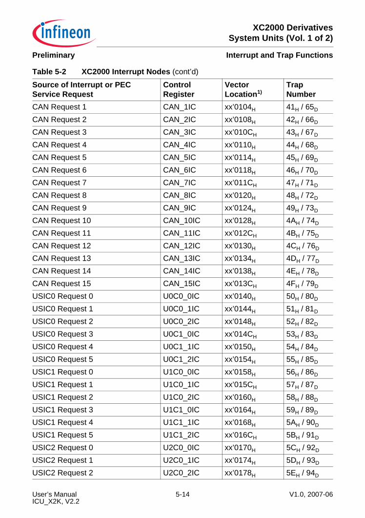
XC2000 DerivativesSystem Units (Vol. 1 of 2)
Interrupt and Trap FunctionsPreliminary
CAN Request 1 CAN_1IC xx’0104H 41H / 65D
CAN Request 2 CAN_2IC xx’0108H 42H / 66D
CAN Request 3 CAN_3IC xx’010CH 43H / 67D
CAN Request 4 CAN_4IC xx’0110H 44H / 68D
CAN Request 5 CAN_5IC xx’0114H 45H / 69D
CAN Request 6 CAN_6IC xx’0118H 46H / 70D
CAN Request 7 CAN_7IC xx’011CH 47H / 71D
CAN Request 8 CAN_8IC xx’0120H 48H / 72D
CAN Request 9 CAN_9IC xx’0124H 49H / 73D
CAN Request 10 CAN_10IC xx’0128H 4AH / 74D
CAN Request 11 CAN_11IC xx’012CH 4BH / 75D
CAN Request 12 CAN_12IC xx’0130H 4CH / 76D
CAN Request 13 CAN_13IC xx’0134H 4DH / 77D
CAN Request 14 CAN_14IC xx’0138H 4EH / 78D
CAN Request 15 CAN_15IC xx’013CH 4FH / 79D
USIC0 Request 0 U0C0_0IC xx’0140H 50H / 80D
USIC0 Request 1 U0C0_1IC xx’0144H 51H / 81D
USIC0 Request 2 U0C0_2IC xx’0148H 52H / 82D
USIC0 Request 3 U0C1_0IC xx’014CH 53H / 83D
USIC0 Request 4 U0C1_1IC xx’0150H 54H / 84D
USIC0 Request 5 U0C1_2IC xx’0154H 55H / 85D
USIC1 Request 0 U1C0_0IC xx’0158H 56H / 86D
USIC1 Request 1 U1C0_1IC xx’015CH 57H / 87D
USIC1 Request 2 U1C0_2IC xx’0160H 58H / 88D
USIC1 Request 3 U1C1_0IC xx’0164H 59H / 89D
USIC1 Request 4 U1C1_1IC xx’0168H 5AH / 90D
USIC1 Request 5 U1C1_2IC xx’016CH 5BH / 91D
USIC2 Request 0 U2C0_0IC xx’0170H 5CH / 92D
USIC2 Request 1 U2C0_1IC xx’0174H 5DH / 93D
USIC2 Request 2 U2C0_2IC xx’0178H 5EH / 94D
Table 5-2 XC2000 Interrupt Nodes (cont’d)
Source of Interrupt or PEC Service Request
Control Register
Vector Location1)
Trap Number
User’s Manual 5-14 V1.0, 2007-06ICU_X2K, V2.2

XC2000 DerivativesSystem Units (Vol. 1 of 2)
Interrupt and Trap FunctionsPreliminary
USIC2 Request 3 U2C1_0IC xx’017CH 5FH / 95D
USIC2 Request 4 U2C1_1IC xx’0180H 60H / 96D
USIC2 Request 5 U2C1_2IC xx’0184H 61H / 97D
Unassigned node – xx’0188H 62H / 98D
Unassigned node – xx’018CH 63H / 99D
Unassigned node – xx’0190H 64H / 100D
Unassigned node – xx’0194H 65H / 101D
Unassigned node – xx’0198H 66H / 102D
Unassigned node – xx’019CH 67H / 103D
Unassigned node – xx’01A0H 68H / 104D
Unassigned node – xx’01A4H 69H / 105D
Unassigned node – xx’01A8H 6AH / 106D
SCU Request 1 SCU_1IC xx’01ACH 6BH / 107D
SCU Request 0 SCU_0IC xx’01B0H 6CH / 108D
Program Flash Modules PFM_IC xx’01B4H 6DH / 109D
RTC RTC_IC xx’01B8H 6EH / 110D
End of PEC Subchannel EOPIC xx’01BCH 6FH / 111D
1) Register VECSEG defines the segment where the vector table is located to.Bitfield VECSC in register CPUCON1 defines the distance between two adjacent vectors. This tablerepresents the default setting, with a distance of 4 (two words) between two vectors.
Table 5-2 XC2000 Interrupt Nodes (cont’d)
Source of Interrupt or PEC Service Request
Control Register
Vector Location1)
Trap Number
User’s Manual 5-15 V1.0, 2007-06ICU_X2K, V2.2
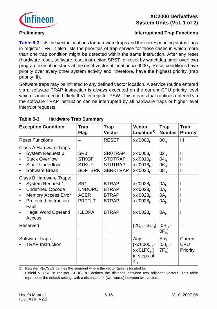
XC2000 DerivativesSystem Units (Vol. 1 of 2)
Interrupt and Trap FunctionsPreliminary
Table 5-3 lists the vector locations for hardware traps and the corresponding status flagsin register TFR. It also lists the priorities of trap service for those cases in which morethan one trap condition might be detected within the same instruction. After any reset(hardware reset, software reset instruction SRST, or reset by watchdog timer overflow)program execution starts at the reset vector at location xx’0000H. Reset conditions havepriority over every other system activity and, therefore, have the highest priority (trappriority III).Software traps may be initiated to any defined vector location. A service routine enteredvia a software TRAP instruction is always executed on the current CPU priority levelwhich is indicated in bitfield ILVL in register PSW. This means that routines entered viathe software TRAP instruction can be interrupted by all hardware traps or higher levelinterrupt requests.
Table 5-3 Hardware Trap SummaryException Condition Trap
FlagTrapVector
Vector Location1)
1) Register VECSEG defines the segment where the vector table is located to.Bitfield VECSC in register CPUCON1 defines the distance between two adjacent vectors. This tablerepresents the default setting, with a distance of 4 (two words) between two vectors.
Trap Number
Trap Priority
Reset Functions – RESET xx’0000H 00H IIIClass A Hardware Traps:• System Request 0• Stack Overflow• Stack Underflow• Software Break
SR0STKOFSTKUFSOFTBRK
SR0TRAPSTOTRAPSTUTRAPSBRKTRAP
xx’0008Hxx’0010Hxx’0018Hxx’0020H
02H04H06H08H
IIIIIIII
Class B Hardware Traps:• System Request 1• Undefined Opcode• Memory Access Error• Protected Instruction
Fault• Illegal Word Operand
Access
SR1UNDOPCACERPRTFLT
ILLOPA
BTRAPBTRAPBTRAPBTRAP
BTRAP
xx’0028Hxx’0028Hxx’0028Hxx’0028H
xx’0028H
0AH0AH0AH0AH
0AH
IIII
I
Reserved – – [2CH - 3CH] [0BH - 0FH]
–
Software Traps:• TRAP Instruction
– – Any[xx’0000H - xx’01FCH] in steps of 4H
Any[00H - 7FH]
Current CPU Priority
User’s Manual 5-16 V1.0, 2007-06ICU_X2K, V2.2
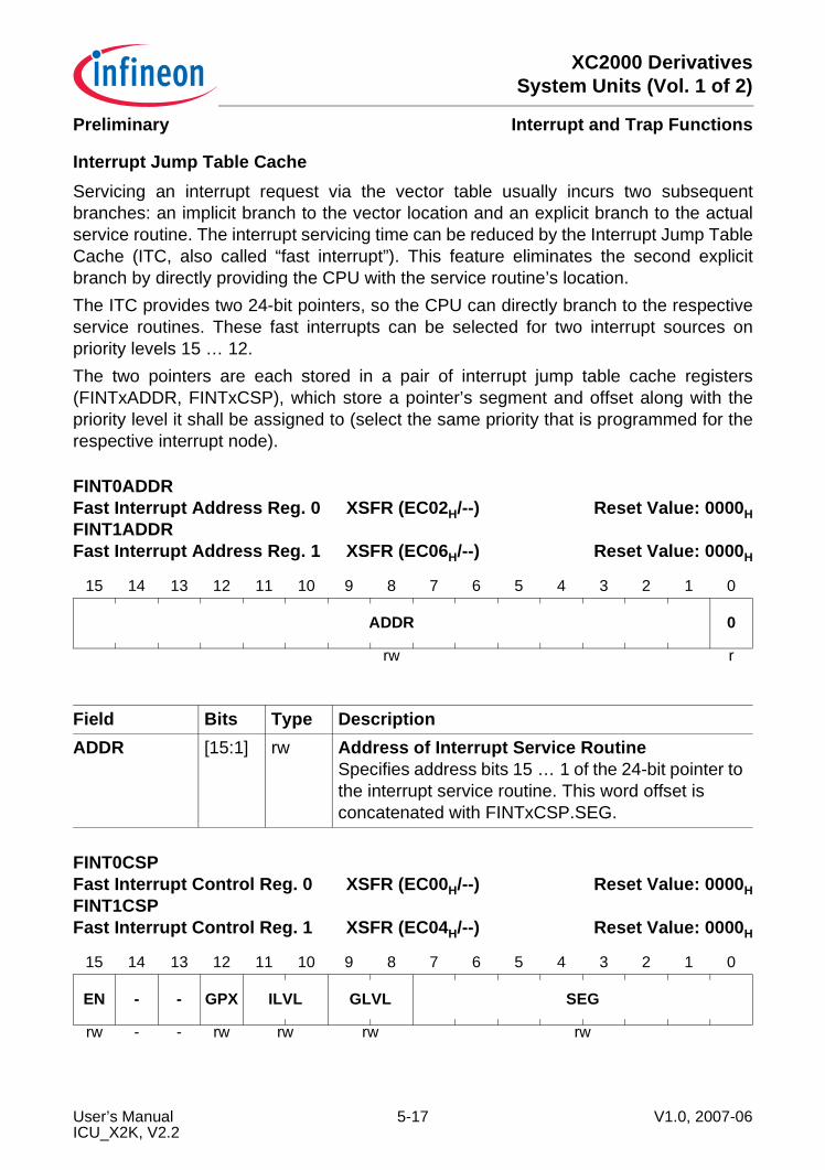
XC2000 DerivativesSystem Units (Vol. 1 of 2)
Interrupt and Trap FunctionsPreliminary
Interrupt Jump Table Cache Servicing an interrupt request via the vector table usually incurs two subsequentbranches: an implicit branch to the vector location and an explicit branch to the actualservice routine. The interrupt servicing time can be reduced by the Interrupt Jump TableCache (ITC, also called “fast interrupt”). This feature eliminates the second explicitbranch by directly providing the CPU with the service routine’s location.The ITC provides two 24-bit pointers, so the CPU can directly branch to the respectiveservice routines. These fast interrupts can be selected for two interrupt sources onpriority levels 15 … 12.The two pointers are each stored in a pair of interrupt jump table cache registers(FINTxADDR, FINTxCSP), which store a pointer’s segment and offset along with thepriority level it shall be assigned to (select the same priority that is programmed for therespective interrupt node).
FINT0ADDR Fast Interrupt Address Reg. 0 XSFR (EC02H/--) Reset Value: 0000HFINT1ADDRFast Interrupt Address Reg. 1 XSFR (EC06H/--) Reset Value: 0000H
15 14 13 12 11 10 9 8 7 6 5 4 3 2 1 0
ADDR 0
rw r
Field Bits Type DescriptionADDR [15:1] rw Address of Interrupt Service Routine
Specifies address bits 15 … 1 of the 24-bit pointer to the interrupt service routine. This word offset is concatenated with FINTxCSP.SEG.
FINT0CSP Fast Interrupt Control Reg. 0 XSFR (EC00H/--) Reset Value: 0000HFINT1CSPFast Interrupt Control Reg. 1 XSFR (EC04H/--) Reset Value: 0000H
15 14 13 12 11 10 9 8 7 6 5 4 3 2 1 0
EN - - GPX ILVL GLVL SEG
rw - - rw rw rw rw
User’s Manual 5-17 V1.0, 2007-06ICU_X2K, V2.2
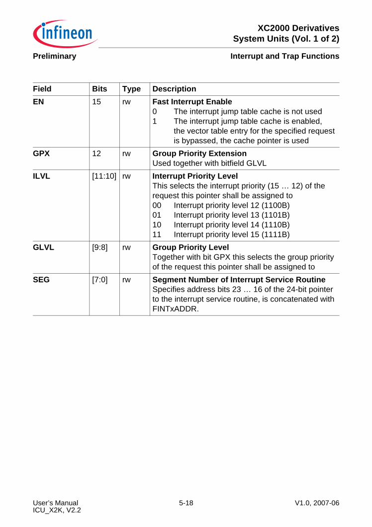
XC2000 DerivativesSystem Units (Vol. 1 of 2)
Interrupt and Trap FunctionsPreliminary
Field Bits Type DescriptionEN 15 rw Fast Interrupt Enable
0 The interrupt jump table cache is not used1 The interrupt jump table cache is enabled,
the vector table entry for the specified request is bypassed, the cache pointer is used
GPX 12 rw Group Priority ExtensionUsed together with bitfield GLVL
ILVL [11:10] rw Interrupt Priority LevelThis selects the interrupt priority (15 … 12) of the request this pointer shall be assigned to00 Interrupt priority level 12 (1100B)01 Interrupt priority level 13 (1101B)10 Interrupt priority level 14 (1110B)11 Interrupt priority level 15 (1111B)
GLVL [9:8] rw Group Priority LevelTogether with bit GPX this selects the group priority of the request this pointer shall be assigned to
SEG [7:0] rw Segment Number of Interrupt Service RoutineSpecifies address bits 23 … 16 of the 24-bit pointer to the interrupt service routine, is concatenated with FINTxADDR.
User’s Manual 5-18 V1.0, 2007-06ICU_X2K, V2.2
XC2000 DerivativesSystem Units (Vol. 1 of 2)
Interrupt and Trap FunctionsPreliminary
5.4 Operation of the Peripheral Event Controller Channels The XC2000’s Peripheral Event Controller (PEC) provides 8 PEC service channelswhich move a single byte or word between any two locations. A PEC transfer can betriggered by an interrupt service request and is the fastest possible interrupt response.In many cases a PEC transfer is sufficient to service the respective peripheral request(for example, serial channels, etc.).PEC transfers do not change the current context, but rather “steal” cycles from the CPU,so the current program status and context needs not to be saved and restored as withstandard interrupts.The PEC channels are controlled by a dedicated set of registers which are assigned todedicated PEC resources:• A 24-bit source pointer for each channel• A 24-bit destination pointer for each channel• A Channel Counter/Control register (PECCx) for each channel, selecting the
operating mode for the respective channel• Two interrupt control registers to control the operation of block transfers
5.4.1 The PECC RegistersThe PECC registers control the action performed by the respective PEC channel.Transfer Size (bit BWT) controls whether a byte or a word is moved during a PECservice cycle. This selection controls the transferred data size and the increment step forthe pointer(s) to be modified.Pointer Modification (bitfield INC) controls, which of the PEC pointers is incrementedafter the PEC transfer. If the pointers are not modified (INC = 00B), the respectivechannel will always move data from the same source to the same destination.Transfer Control (bitfield COUNT) controls if the respective PEC channel remainsactive after the transfer or not. Bitfield COUNT also generally enables a PEC channel(COUNT > 00H).The PECC registers also select the assignment of PEC channels to interrupt prioritylevels (bitfield PLEV) and the interrupt behavior after PEC transfer completion (bitEOPINT).Note: All interrupt request sources that are enabled and programmed for PEC service
should use different channels. Otherwise, only one transfer will be performed forall simultaneous requests. When COUNT is decremented to 00H, and the CPU isto be interrupted, an incorrect interrupt vector will be generated.PEC transfers are executed only if their priority level is higher than the CPU level.
User’s Manual 5-19 V1.0, 2007-06ICU_X2K, V2.2
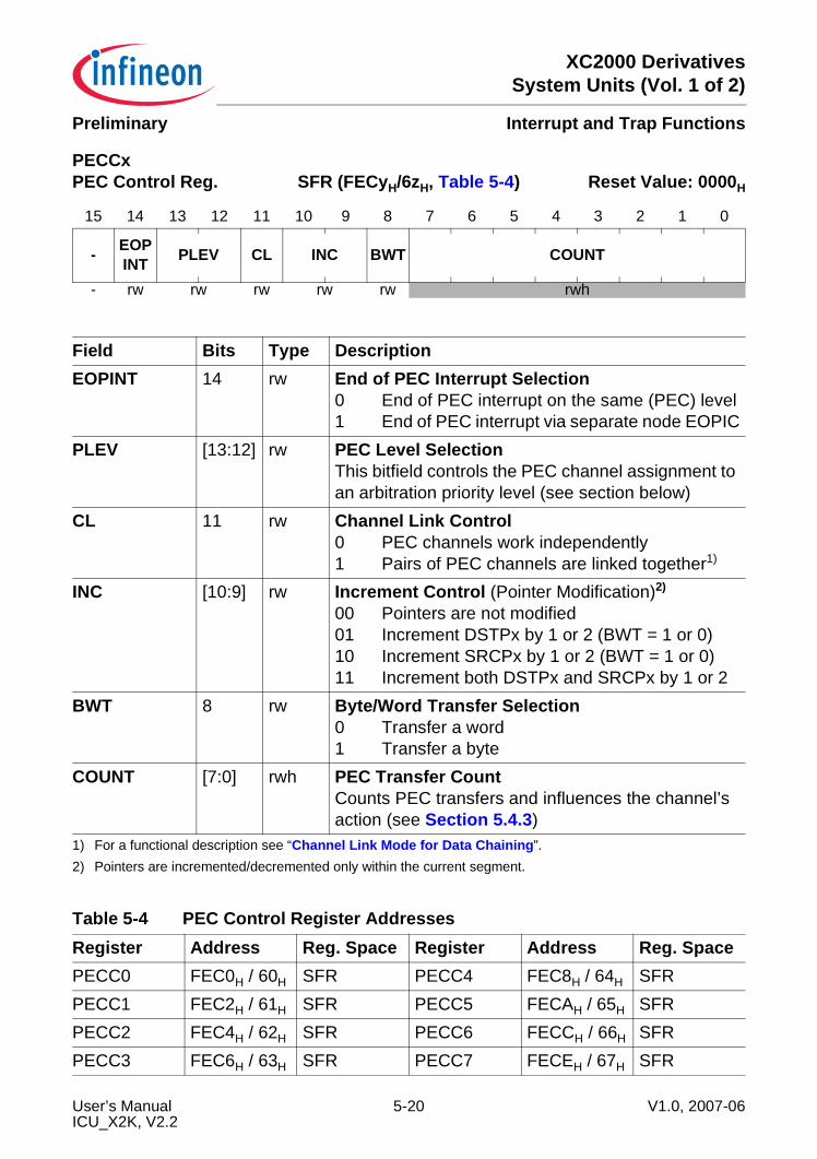
XC2000 DerivativesSystem Units (Vol. 1 of 2)
Interrupt and Trap FunctionsPreliminary
PECCx PEC Control Reg. SFR (FECyH/6zH, Table 5-4) Reset Value: 0000H
15 14 13 12 11 10 9 8 7 6 5 4 3 2 1 0
- EOP INT PLEV CL INC BWT COUNT
- rw rw rw rw rw rwh
Field Bits Type DescriptionEOPINT 14 rw End of PEC Interrupt Selection
0 End of PEC interrupt on the same (PEC) level1 End of PEC interrupt via separate node EOPIC
PLEV [13:12] rw PEC Level SelectionThis bitfield controls the PEC channel assignment to an arbitration priority level (see section below)
CL 11 rw Channel Link Control0 PEC channels work independently1 Pairs of PEC channels are linked together1)
1) For a functional description see “Channel Link Mode for Data Chaining”.
INC [10:9] rw Increment Control (Pointer Modification)2)
00 Pointers are not modified01 Increment DSTPx by 1 or 2 (BWT = 1 or 0)10 Increment SRCPx by 1 or 2 (BWT = 1 or 0)11 Increment both DSTPx and SRCPx by 1 or 2
2) Pointers are incremented/decremented only within the current segment.
BWT 8 rw Byte/Word Transfer Selection0 Transfer a word1 Transfer a byte
COUNT [7:0] rwh PEC Transfer CountCounts PEC transfers and influences the channel’s action (see Section 5.4.3)
Table 5-4 PEC Control Register AddressesRegister Address Reg. Space Register Address Reg. SpacePECC0 FEC0H / 60H SFR PECC4 FEC8H / 64H SFRPECC1 FEC2H / 61H SFR PECC5 FECAH / 65H SFRPECC2 FEC4H / 62H SFR PECC6 FECCH / 66H SFRPECC3 FEC6H / 63H SFR PECC7 FECEH / 67H SFR
User’s Manual 5-20 V1.0, 2007-06ICU_X2K, V2.2

XC2000 DerivativesSystem Units (Vol. 1 of 2)
Interrupt and Trap FunctionsPreliminary
The PEC channel number is derived from the respective ILVL (LSB) and GLVL, wherethe priority band (ILVL) is selected by the channel’s bitfield PLEV (see Table 5-5). So,programming a source to priority level 15 (ILVL = 1111B) selects the PEC channel group7 … 4 with PLEV = 00B; programming a source to priority level 14 (ILVL = 1110B) selectsthe PEC channel group 3 … 0 with PLEV = 00B; programming a source to priority level10 (ILVL = 1010B) selects the PEC channel group 3 … 0 with PLEV = 10B. The actualPEC channel number is then determined by the group priority (levels 3 … 0, i.e.GPX = 0).Simultaneous requests for PEC channels are prioritized according to the PEC channelnumber, where channel 0 has lowest and channel 7 has highest priority.Note: All sources requesting PEC service must be programmed to different PEC
channels. Otherwise, an incorrect PEC channel may be activated.
Table 5-6 shows in a few examples which action is executed with a given programmingof an interrupt control register and a PEC channel.
Table 5-5 PEC Channel AssignmentSelected PEC Channel
Group Level
Used Interrupt Priorities Depending on Bitfield PLEVPLEV = 00B PLEV = 01B PLEV = 10B PLEV = 11B
7 3 15 13 11 96 25 14 03 3 14 12 10 82 21 10 0
User’s Manual 5-21 V1.0, 2007-06ICU_X2K, V2.2
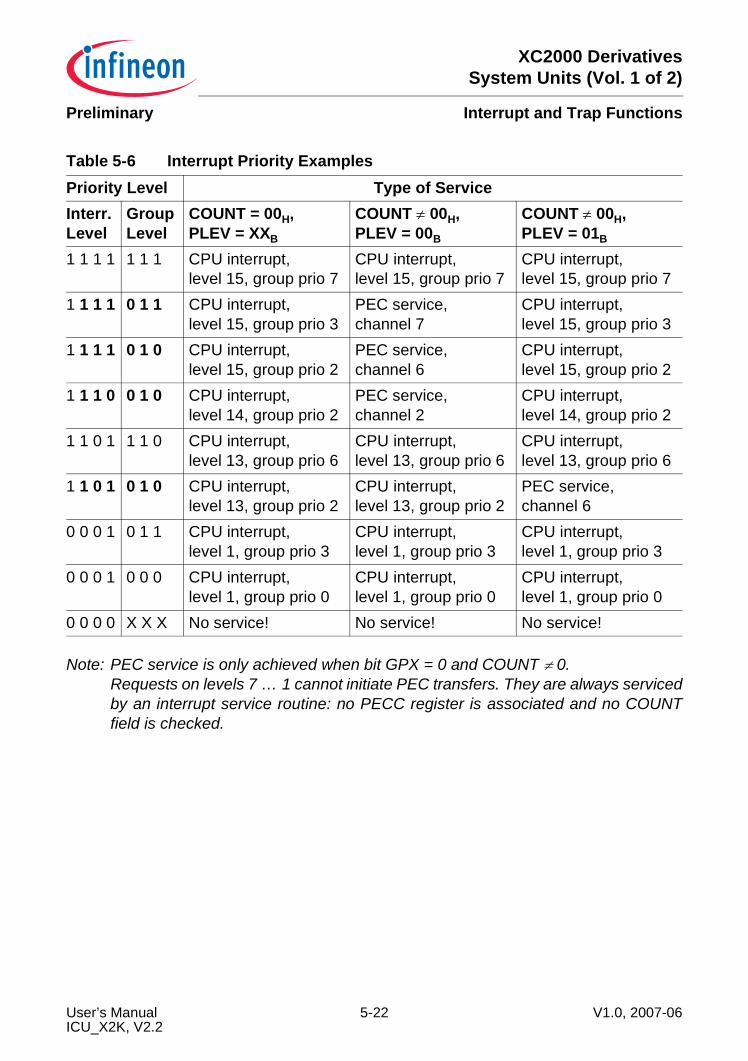
XC2000 DerivativesSystem Units (Vol. 1 of 2)
Interrupt and Trap FunctionsPreliminary
Note: PEC service is only achieved when bit GPX = 0 and COUNT ≠ 0.Requests on levels 7 … 1 cannot initiate PEC transfers. They are always servicedby an interrupt service routine: no PECC register is associated and no COUNTfield is checked.
Table 5-6 Interrupt Priority ExamplesPriority Level Type of ServiceInterr. Level
Group Level
COUNT = 00H,PLEV = XXB
COUNT ≠ 00H,PLEV = 00B
COUNT ≠ 00H,PLEV = 01B
1 1 1 1 1 1 1 CPU interrupt,level 15, group prio 7
CPU interrupt,level 15, group prio 7
CPU interrupt,level 15, group prio 7
1 1 1 1 0 1 1 CPU interrupt,level 15, group prio 3
PEC service,channel 7
CPU interrupt,level 15, group prio 3
1 1 1 1 0 1 0 CPU interrupt,level 15, group prio 2
PEC service,channel 6
CPU interrupt,level 15, group prio 2
1 1 1 0 0 1 0 CPU interrupt,level 14, group prio 2
PEC service,channel 2
CPU interrupt,level 14, group prio 2
1 1 0 1 1 1 0 CPU interrupt,level 13, group prio 6
CPU interrupt,level 13, group prio 6
CPU interrupt,level 13, group prio 6
1 1 0 1 0 1 0 CPU interrupt,level 13, group prio 2
CPU interrupt,level 13, group prio 2
PEC service,channel 6
0 0 0 1 0 1 1 CPU interrupt,level 1, group prio 3
CPU interrupt,level 1, group prio 3
CPU interrupt,level 1, group prio 3
0 0 0 1 0 0 0 CPU interrupt,level 1, group prio 0
CPU interrupt,level 1, group prio 0
CPU interrupt,level 1, group prio 0
0 0 0 0 X X X No service! No service! No service!
User’s Manual 5-22 V1.0, 2007-06ICU_X2K, V2.2
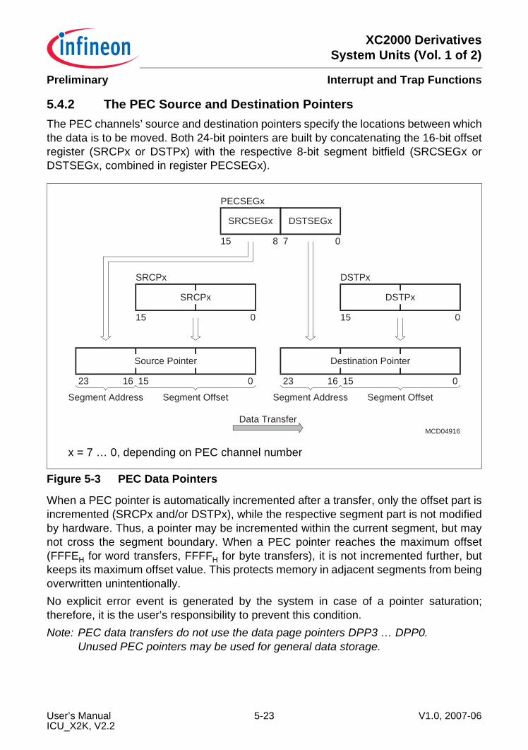
XC2000 DerivativesSystem Units (Vol. 1 of 2)
Interrupt and Trap FunctionsPreliminary
5.4.2 The PEC Source and Destination PointersThe PEC channels’ source and destination pointers specify the locations between whichthe data is to be moved. Both 24-bit pointers are built by concatenating the 16-bit offsetregister (SRCPx or DSTPx) with the respective 8-bit segment bitfield (SRCSEGx orDSTSEGx, combined in register PECSEGx).
Figure 5-3 PEC Data Pointers
When a PEC pointer is automatically incremented after a transfer, only the offset part isincremented (SRCPx and/or DSTPx), while the respective segment part is not modifiedby hardware. Thus, a pointer may be incremented within the current segment, but maynot cross the segment boundary. When a PEC pointer reaches the maximum offset(FFFEH for word transfers, FFFFH for byte transfers), it is not incremented further, butkeeps its maximum offset value. This protects memory in adjacent segments from beingoverwritten unintentionally.No explicit error event is generated by the system in case of a pointer saturation;therefore, it is the user’s responsibility to prevent this condition.Note: PEC data transfers do not use the data page pointers DPP3 … DPP0.
Unused PEC pointers may be used for general data storage.
x = 7 … 0, depending on PEC channel number
MCD04916
Source Pointer
23 16 15 0
Segment Address Segment Offset
Destination Pointer
23 16 15 0
Segment Address Segment Offset
SRCPx
15 0
SRCPx
DSTPx
15 0
DSTPx
DSTSEGx
7 0
SRCSEGx
15 8
PECSEGx
Data Transfer
User’s Manual 5-23 V1.0, 2007-06ICU_X2K, V2.2
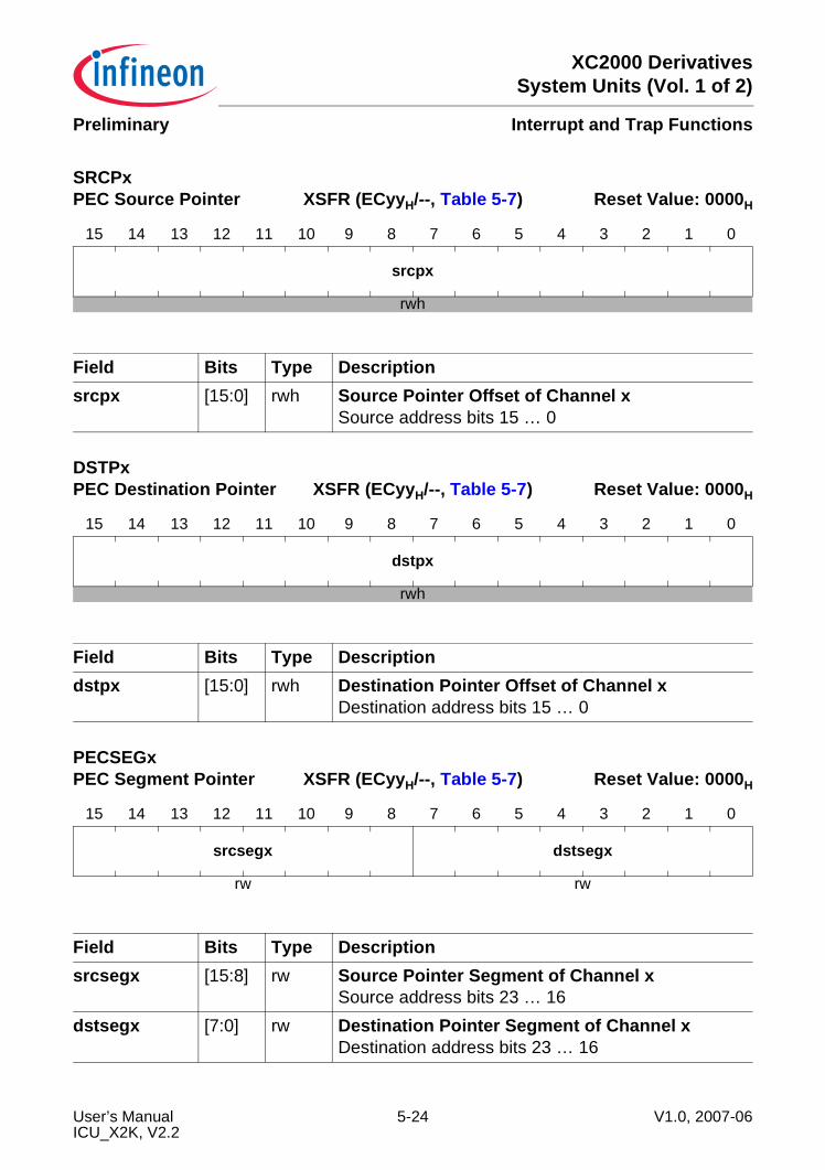
XC2000 DerivativesSystem Units (Vol. 1 of 2)
Interrupt and Trap FunctionsPreliminary
SRCPx PEC Source Pointer XSFR (ECyyH/--, Table 5-7) Reset Value: 0000H
15 14 13 12 11 10 9 8 7 6 5 4 3 2 1 0
srcpx
rwh
Field Bits Type Descriptionsrcpx [15:0] rwh Source Pointer Offset of Channel x
Source address bits 15 … 0
DSTPx PEC Destination Pointer XSFR (ECyyH/--, Table 5-7) Reset Value: 0000H
15 14 13 12 11 10 9 8 7 6 5 4 3 2 1 0
dstpx
rwh
Field Bits Type Descriptiondstpx [15:0] rwh Destination Pointer Offset of Channel x
Destination address bits 15 … 0
PECSEGx PEC Segment Pointer XSFR (ECyyH/--, Table 5-7) Reset Value: 0000H
15 14 13 12 11 10 9 8 7 6 5 4 3 2 1 0
srcsegx dstsegx
rw rw
Field Bits Type Descriptionsrcsegx [15:8] rw Source Pointer Segment of Channel x
Source address bits 23 … 16dstsegx [7:0] rw Destination Pointer Segment of Channel x
Destination address bits 23 … 16
User’s Manual 5-24 V1.0, 2007-06ICU_X2K, V2.2
XC2000 DerivativesSystem Units (Vol. 1 of 2)
Interrupt and Trap FunctionsPreliminary
Note: If word data transfer is selected for a specific PEC channel (BWT = 0), therespective source and destination pointers must both contain a valid word addresswhich points to an even byte boundary. Otherwise, the Illegal Word Access trapwill be invoked when this channel is used.
5.4.3 PEC Transfer ControlThe PEC Transfer Count Field COUNT controls the behavior of the respective PECchannel. The contents of bitfield COUNT select the action to be taken at the time therequest is activated. COUNT may allow a specified number of PEC transfers, unlimitedtransfers, or no PEC service at all. Table 5-8 summarizes, how the COUNT field, theinterrupt requests flag IR, and the PEC channel action depend on the previous contentsof COUNT.
Table 5-7 PEC Data Pointer Register AddressesChannel # 0 1 2 3 4 5 6 7PECSEGx EC80H EC82H EC84H EC86H EC88H EC8AH EC8CH EC8EH
SRCPx EC40H EC44H EC48H EC4CH EC50H EC54H EC58H EC5CH
DSTPx EC42H EC46H EC4AH EC4EH EC52H EC56H EC5AH EC5EH
Table 5-8 Influence of Bitfield COUNTPrevious COUNT
Modified COUNT
IR after Service
Action of PEC Channel and Comments
FFH FFH 0 Move a Byte/WordContinuous transfer mode, i.e. COUNT is not modified
FEH … 02H FDH … 01H 0 Move a Byte/Word and decrement COUNT01H 00H 1 EOPINT = 0 (channel-specific interrupt)
Move a Byte/Word and leave request flag set, which triggers another request
0 EOPINT = 1 (separate end-of-PEC interrupt)Move a Byte/Word and clear request flag, set the respective PEC subnode request flag CxIR instead1)
1) Setting a subnode request flag also sets flag EOPIR if the subnode request is enabled (CxIE = 1).
00H 00H – No PEC action!Activate interrupt service routine rather than PEC channel
User’s Manual 5-25 V1.0, 2007-06ICU_X2K, V2.2
XC2000 DerivativesSystem Units (Vol. 1 of 2)
Interrupt and Trap FunctionsPreliminary
The PEC transfer counter allows service of a specified number of requests by therespective PEC channel, and then (when COUNT reaches 00H) activation of an interruptservice routine, either associated with the PEC channel’s priority level or with the generalend-of-PEC interrupt. After each PEC transfer, the COUNT field is decremented (exceptfor COUNT = FFH) and the request flag is cleared to indicate that the request has beenserviced.When COUNT contains the value 00H, the respective PEC channel remains idle and theassociated interrupt service routine is activated instead. This allows servicing requestson all priority levels by standard interrupt service routines.Continuous transfers are selected by the value FFH in bitfield COUNT. In this case,COUNT is not modified and the respective PEC channel services any request until it isdisabled again.When COUNT is decremented from 01H to 00H after a transfer, a standard interrupt isrequested which can then handle the end of the PEC block transfer (channel-specificinterrupt or common end-of-PEC interrupt, see Table 5-8).
User’s Manual 5-26 V1.0, 2007-06ICU_X2K, V2.2
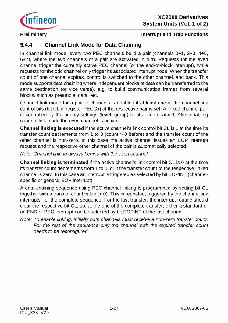
XC2000 DerivativesSystem Units (Vol. 1 of 2)
Interrupt and Trap FunctionsPreliminary
5.4.4 Channel Link Mode for Data ChainingIn channel link mode, every two PEC channels build a pair (channels 0+1, 2+3, 4+5,6+7), where the two channels of a pair are activated in turn. Requests for the evenchannel trigger the currently active PEC channel (or the end-of-block interrupt), whilerequests for the odd channel only trigger its associated interrupt node. When the transfercount of one channel expires, control is switched to the other channel, and back. Thismode supports data chaining where independent blocks of data can be transferred to thesame destination (or vice versa), e.g. to build communication frames from severalblocks, such as preamble, data, etc.Channel link mode for a pair of channels is enabled if at least one of the channel linkcontrol bits (bit CL in register PECCx) of the respective pair is set. A linked channel pairis controlled by the priority-settings (level, group) for its even channel. After enablingchannel link mode the even channel is active.Channel linking is executed if the active channel’s link control bit CL is 1 at the time itstransfer count decrements from 1 to 0 (count > 0 before) and the transfer count of theother channel is non-zero. In this case the active channel issues an EOP interruptrequest and the respective other channel of the pair is automatically selected.Note: Channel linking always begins with the even channel.
Channel linking is terminated if the active channel’s link control bit CL is 0 at the timeits transfer count decrements from 1 to 0, or if the transfer count of the respective linkedchannel is zero. In this case an interrupt is triggered as selected by bit EOPINT (channel-specific or general EOP interrupt).A data-chaining sequence using PEC channel linking is programmed by setting bit CLtogether with a transfer count value (> 0). This is repeated, triggered by the channel linkinterrupts, for the complete sequence. For the last transfer, the interrupt routine shouldclear the respective bit CL, so, at the end of the complete transfer, either a standard oran END of PEC interrupt can be selected by bit EOPINT of the last channel.Note: To enable linking, initially both channels must receive a non-zero transfer count.
For the rest of the sequence only the channel with the expired transfer countneeds to be reconfigured.
User’s Manual 5-27 V1.0, 2007-06ICU_X2K, V2.2
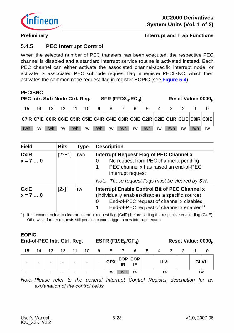
XC2000 DerivativesSystem Units (Vol. 1 of 2)
Interrupt and Trap FunctionsPreliminary
5.4.5 PEC Interrupt ControlWhen the selected number of PEC transfers has been executed, the respective PECchannel is disabled and a standard interrupt service routine is activated instead. EachPEC channel can either activate the associated channel-specific interrupt node, oractivate its associated PEC subnode request flag in register PECISNC, which thenactivates the common node request flag in register EOPIC (see Figure 5-4).
Note: Please refer to the general Interrupt Control Register description for anexplanation of the control fields.
PECISNC PEC Intr. Sub-Node Ctrl. Reg. SFR (FFD8H/ECH) Reset Value: 0000H
15 14 13 12 11 10 9 8 7 6 5 4 3 2 1 0
C7IR C7IE C6IR C6IE C5IR C5IE C4IR C4IE C3IR C3IE C2IR C2IE C1IR C1IE C0IR C0IE
rwh rw rwh rw rwh rw rwh rw rwh rw rwh rw rwh rw rwh rw
Field Bits Type DescriptionCxIRx = 7 … 0
[2x+1] rwh Interrupt Request Flag of PEC Channel x0 No request from PEC channel x pending1 PEC channel x has raised an end-of-PEC
interrupt requestNote: These request flags must be cleared by SW.
CxIEx = 7 … 0
[2x] rw Interrupt Enable Control Bit of PEC Channel x(individually enables/disables a specific source)0 End-of-PEC request of channel x disabled1 End-of-PEC request of channel x enabled1)
1) It is recommended to clear an interrupt request flag (CxIR) before setting the respective enable flag (CxIE).Otherwise, former requests still pending cannot trigger a new interrupt request.
EOPIC End-of-PEC Intr. Ctrl. Reg. ESFR (F19EH/CFH) Reset Value: 0000H
15 14 13 12 11 10 9 8 7 6 5 4 3 2 1 0
- - - - - - - GPX EOPIR
EOPIE ILVL GLVL
- - - - - - - rw rwh rw rw rw
User’s Manual 5-28 V1.0, 2007-06ICU_X2K, V2.2

XC2000 DerivativesSystem Units (Vol. 1 of 2)
Interrupt and Trap FunctionsPreliminary
Figure 5-4 End of PEC Interrupt Sub Node
Note: The interrupt service routine must service and clear all currently active requestsbefore terminating. Requests occurring later will set EOPIR again and the serviceroutine will be re-entered.
MCD04914
C7IR C7IE C6IR C6IE C5IR C5IE C4IR C4IE C3IR C3IE C2IR C2IE C1IR C1IE C0IR C0IE
& & & & & & & &
1
PECISNC
15 0
0 0 0 0 0 0 0 GPX EOPIR
EOPIE ILVL GLVL
15 8 7 0
EOPIC
Interrupt RequestPulse Generator
&
User’s Manual 5-29 V1.0, 2007-06ICU_X2K, V2.2
XC2000 DerivativesSystem Units (Vol. 1 of 2)
Interrupt and Trap FunctionsPreliminary
5.5 Prioritization of Interrupt and PEC Service RequestsInterrupt and PEC service requests from all sources can be enabled so they arearbitrated and serviced (if they win), or they may be disabled, so their requests aredisregarded and not serviced.Enabling and disabling interrupt requests may be done via three mechanisms: • Control Bits• Priority Level• ATOMIC and EXTended InstructionsControl Bits allow switching of each individual source “ON” or “OFF” so that it maygenerate a request or not. The control bits (xxIE) are located in the respective interruptcontrol registers. All interrupt requests may be enabled or disabled generally via bit IENin register PSW. This control bit is the “main switch” which selects if requests from anysource are accepted or not.For a specific request to be arbitrated, the respective source’s enable bit and the globalenable bit must both be set.The Priority Level automatically selects a certain group of interrupt requests to beacknowledged and ignores all other requests. The priority level of the source that wonthe arbitration is compared against the CPU’s current level and the source is servicedonly if its level is higher than the current CPU level. Changing the CPU level to a specificvalue via software blocks all requests on the same or a lower level. An interrupt sourceassigned to level 0 will be disabled and will never be serviced.The ATOMIC and EXTend instructions automatically disable all interrupt requests forthe duration of the following 1 … 4 instructions. This is useful for semaphore handling,for example, and does not require to re-enable the interrupt system after the inseparableinstruction sequence.
Interrupt Class ManagementAn interrupt class covers a set of interrupt sources with the same importance, i.e. thesame priority from the system’s viewpoint. Interrupts of the same class must not interrupteach other. The XC2000 supports this function with two features:Classes with up to eight members can be established by using the same interrupt priority(ILVL) and assigning a dedicated group level to each member. This functionality is built-in and handled automatically by the interrupt controller.Classes with more than eight members can be established by using a number ofadjacent interrupt priorities (ILVL) and the respective group levels (eight per ILVL). Eachinterrupt service routine within this class sets the CPU level to the highest interruptpriority within the class. All requests from the same or any lower level are blocked now,i.e. no request of this class will be accepted.
User’s Manual 5-30 V1.0, 2007-06ICU_X2K, V2.2
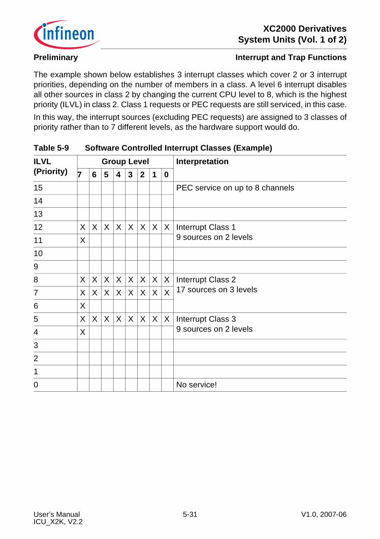
XC2000 DerivativesSystem Units (Vol. 1 of 2)
Interrupt and Trap FunctionsPreliminary
The example shown below establishes 3 interrupt classes which cover 2 or 3 interruptpriorities, depending on the number of members in a class. A level 6 interrupt disablesall other sources in class 2 by changing the current CPU level to 8, which is the highestpriority (ILVL) in class 2. Class 1 requests or PEC requests are still serviced, in this case.In this way, the interrupt sources (excluding PEC requests) are assigned to 3 classes ofpriority rather than to 7 different levels, as the hardware support would do.
Table 5-9 Software Controlled Interrupt Classes (Example)ILVL (Priority)
Group Level Interpretation7 6 5 4 3 2 1 0
15 PEC service on up to 8 channels141312 X X X X X X X X Interrupt Class 1
9 sources on 2 levels11 X1098 X X X X X X X X Interrupt Class 2
17 sources on 3 levels7 X X X X X X X X6 X5 X X X X X X X X Interrupt Class 3
9 sources on 2 levels4 X3210 No service!
User’s Manual 5-31 V1.0, 2007-06ICU_X2K, V2.2
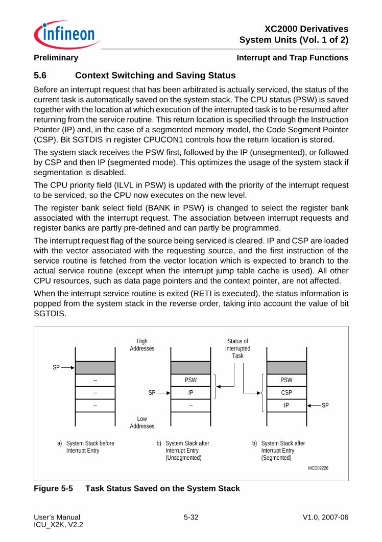
XC2000 DerivativesSystem Units (Vol. 1 of 2)
Interrupt and Trap FunctionsPreliminary
5.6 Context Switching and Saving StatusBefore an interrupt request that has been arbitrated is actually serviced, the status of thecurrent task is automatically saved on the system stack. The CPU status (PSW) is savedtogether with the location at which execution of the interrupted task is to be resumed afterreturning from the service routine. This return location is specified through the InstructionPointer (IP) and, in the case of a segmented memory model, the Code Segment Pointer(CSP). Bit SGTDIS in register CPUCON1 controls how the return location is stored.The system stack receives the PSW first, followed by the IP (unsegmented), or followedby CSP and then IP (segmented mode). This optimizes the usage of the system stack ifsegmentation is disabled.The CPU priority field (ILVL in PSW) is updated with the priority of the interrupt requestto be serviced, so the CPU now executes on the new level.The register bank select field (BANK in PSW) is changed to select the register bankassociated with the interrupt request. The association between interrupt requests andregister banks are partly pre-defined and can partly be programmed.The interrupt request flag of the source being serviced is cleared. IP and CSP are loadedwith the vector associated with the requesting source, and the first instruction of theservice routine is fetched from the vector location which is expected to branch to theactual service routine (except when the interrupt jump table cache is used). All otherCPU resources, such as data page pointers and the context pointer, are not affected.When the interrupt service routine is exited (RETI is executed), the status information ispopped from the system stack in the reverse order, taking into account the value of bitSGTDIS.
Figure 5-5 Task Status Saved on the System Stack
(Unsegmented)
PSW
System Stack afterInterrupt EntryInterrupt Entry
System Stack beforea) b)
SP
HighAddresses
LowAddresses
--
--
--
SP IP
--
MCD02226
b)Interrupt EntrySystem Stack after
(Segmented)
TaskInterruptedStatus of
CSP
PSW
IP SP
User’s Manual 5-32 V1.0, 2007-06ICU_X2K, V2.2
XC2000 DerivativesSystem Units (Vol. 1 of 2)
Interrupt and Trap FunctionsPreliminary
Context Switching An interrupt service routine usually saves all the registers it uses on the stack andrestores them before returning. The more registers a routine uses, the more time is spentsaving and restoring. The XC2000 allows switching the complete bank of CPU registers(GPRs) either automatically or with a single instruction, so the service routine executeswithin its own separate context (see also Section 4.5.2).There are two ways to switch the context in the XC2000 core:Switching Context of the Global Register Bank changes the complete global registerbank of CPU registers (GPRs) by changing the Context Pointer with a single instruction,so the service routine executes within its own separate context. The instruction “SCXTCP, #New_Bank” pushes the contents of the context pointer (CP) on the system stackand loads CP with the immediate value “New_Bank”; this in turn, selects a new registerbank. The service routine may now use its “own registers”. This register bank ispreserved when the service routine terminates, i.e. its contents are available on the nextcall. Before returning (RETI), the previous CP is simply POPped from the system stack,which returns the registers to the original global bank.Resources used by the interrupting program, such as the DPPs, must eventually besaved and restored.Note: There are certain timing restrictions during context switching that are associated
with pipeline behavior.
Switching Context by changing the selected register bank automatically updatesbitfield BANK to select one of the two local register banks or the current global registerbank, so the service routine may now use its “own registers” directly. This local registerbank is preserved when the service routine is terminated; thus, its contents are availableon the next call.When switching to the global register bank, the service routine usually must also switchthe context of the global register bank to get a private set of GPRs, because the globalbank is likely to be used by several tasks.For interrupt priority levels 15 … 12 the target register bank can be pre-selected andthen be switched automatically. The register bank selection registers BNKSELx providea 2-bit field for each possible arbitration priority level. The respective bitfield is thencopied to bitfield BANK in register PSW to select the register bank, as soon as therespective interrupt request is accepted.Table 5-10 identifies the arbitration priority level assignment to the respective bitfieldswithin the four register bank selection registers.
User’s Manual 5-33 V1.0, 2007-06ICU_X2K, V2.2
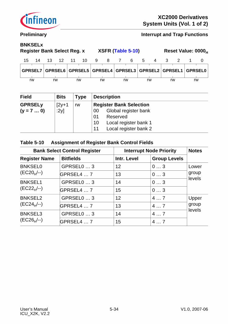
XC2000 DerivativesSystem Units (Vol. 1 of 2)
Interrupt and Trap FunctionsPreliminary
BNKSELx Register Bank Select Reg. x XSFR (Table 5-10) Reset Value: 0000H
15 14 13 12 11 10 9 8 7 6 5 4 3 2 1 0
GPRSEL7 GPRSEL6 GPRSEL5 GPRSEL4 GPRSEL3 GPRSEL2 GPRSEL1 GPRSEL0
rw rw rw rw rw rw rw rw
Field Bits Type DescriptionGPRSELy(y = 7 … 0)
[2y+1:2y]
rw Register Bank Selection00 Global register bank01 Reserved10 Local register bank 111 Local register bank 2
Table 5-10 Assignment of Register Bank Control FieldsBank Select Control Register Interrupt Node Priority Notes
Register Name Bitfields Intr. Level Group LevelsBNKSEL0(EC20H/--)
GPRSEL0 … 3 12 0 … 3 Lower group levels
GPRSEL4 … 7 13 0 … 3BNKSEL1(EC22H/--)
GPRSEL0 … 3 14 0 … 3GPRSEL4 … 7 15 0 … 3
BNKSEL2(EC24H/--)
GPRSEL0 … 3 12 4 … 7 Upper group levels
GPRSEL4 … 7 13 4 … 7BNKSEL3(EC26H/--)
GPRSEL0 … 3 14 4 … 7GPRSEL4 … 7 15 4 … 7
User’s Manual 5-34 V1.0, 2007-06ICU_X2K, V2.2
XC2000 DerivativesSystem Units (Vol. 1 of 2)
Interrupt and Trap FunctionsPreliminary
5.7 Interrupt Node Sharing Interrupt nodes may be shared among several module requests if either the requests aregenerated mutually exclusively or the requests are generated at a low rate. If more thanone source is enabled in this case, the interrupt handler will first need to determine therequesting source. However, this overhead is not critical for low rate requests.This node sharing is either controlled via interrupt sub-node control registers (ISNC)which provide separate request flags and enable bits for each supported request source,or via register ISSR, where each bit selects one of two interrupt sources. The interruptlevel used for arbitration is determined by the node control register (… IC).The specific request flags within ISNC registers must be reset by software, contrary tothe node request bits which are cleared automatically.
Table 5-11 Sub-Node Control Bit AllocationInterrupt Node Interrupt Sources ControlEOPIC PEC channels 7 … 0 PECISNCRTC_IC RTC: overflow of T14, CNT0 … CNT3 RTC_ISNCCC2_CC16IC CAPCOM2 request, ERU request 0 ISSRCC2_CC17IC CAPCOM2 request, ERU request 1 ISSRCC2_CC18IC CAPCOM2 request, ERU request 2 ISSRCC2_CC19IC CAPCOM2 request, ERU request 3 ISSRCC2_CC20IC CAPCOM2 request, USIC0 request 6 ISSRCC2_CC21IC CAPCOM2 request, USIC0 request 7 ISSRCC2_CC22IC CAPCOM2 request, USIC1 request 6 ISSRCC2_CC23IC CAPCOM2 request, USIC1 request 7 ISSRCC2_CC24IC CAPCOM2 request, ERU request 0 ISSRCC2_CC25IC CAPCOM2 request, ERU request 1 ISSRCC2_CC26IC CAPCOM2 request, ERU request 2 ISSRCC2_CC27IC CAPCOM2 request, ERU request 3 ISSRCC2_CC28IC CAPCOM2 request, USIC2 request 6 ISSRCC2_CC29IC CAPCOM2 request, USIC2 request 7 ISSR
User’s Manual 5-35 V1.0, 2007-06ICU_X2K, V2.2
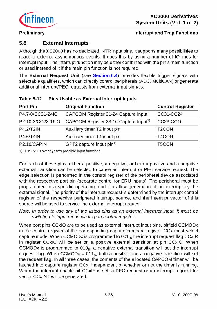
XC2000 DerivativesSystem Units (Vol. 1 of 2)
Interrupt and Trap FunctionsPreliminary
5.8 External Interrupts Although the XC2000 has no dedicated INTR input pins, it supports many possibilities toreact to external asynchronous events. It does this by using a number of IO lines forinterrupt input. The interrupt function may be either combined with the pin’s main functionor used instead of it if the main pin function is not required.The External Request Unit (see Section 6.4) provides flexible trigger signals withselectable qualifiers, which can directly control peripherals (ADC, MultiCAN) or generateadditional interrupt/PEC requests from external input signals.
For each of these pins, either a positive, a negative, or both a positive and a negativeexternal transition can be selected to cause an interrupt or PEC service request. Theedge selection is performed in the control register of the peripheral device associatedwith the respective port pin (separate control for ERU inputs). The peripheral must beprogrammed to a specific operating mode to allow generation of an interrupt by theexternal signal. The priority of the interrupt request is determined by the interrupt controlregister of the respective peripheral interrupt source, and the interrupt vector of thissource will be used to service the external interrupt request.Note: In order to use any of the listed pins as an external interrupt input, it must be
switched to input mode via its port control register.
When port pins CCxIO are to be used as external interrupt input pins, bitfield CCMODxin the control register of the corresponding capture/compare register CCx must selectcapture mode. When CCMODx is programmed to 001B, the interrupt request flag CCxIRin register CCxIC will be set on a positive external transition at pin CCxIO. WhenCCMODx is programmed to 010B, a negative external transition will set the interruptrequest flag. When CCMODx = 011B, both a positive and a negative transition will setthe request flag. In all three cases, the contents of the allocated CAPCOM timer will belatched into capture register CCx, independent of whether or not the timer is running.When the interrupt enable bit CCxIE is set, a PEC request or an interrupt request forvector CCxINT will be generated.
Table 5-12 Pins Usable as External Interrupt InputsPort Pin Original Function Control RegisterP4.7-0/CC31-24IO CAPCOM Register 31-24 Capture Input CC31-CC24P2.10-3/CC23-16IO CAPCOM Register 23-16 Capture Input1)
1) Pin P2.10 overlays two possible input functions.
CC23-CC16P4.2/T2IN Auxiliary timer T2 input pin T2CONP4.6/T4IN Auxiliary timer T4 input pin T4CONP2.10/CAPIN GPT2 capture input pin1) T5CON
User’s Manual 5-36 V1.0, 2007-06ICU_X2K, V2.2
XC2000 DerivativesSystem Units (Vol. 1 of 2)
Interrupt and Trap FunctionsPreliminary
Pins T2IN or T4IN can be used as external interrupt input pins when the associatedauxiliary timer T2 or T4 in block GPT1 is configured for capture mode. This mode isselected by programming the mode control fields T2M or T4M in control registersT2CON or T4CON to 101B. The active edge of the external input signal is determined bybitfields T2I or T4I. When these fields are programmed to X01B, interrupt request flagsT2IR or T4IR in registers T2IC or T4IC will be set on a positive external transition at pinsT2IN or T4IN, respectively. When T2I or T4I is programmed to X10B, then a negativeexternal transition will set the corresponding request flag. When T2I or T4I isprogrammed to X11B, both a positive and a negative transition will set the request flag.In all three cases, the contents of the core timer T3 will be captured into the auxiliarytimer registers T2 or T4 based on the transition at pins T2IN or T4IN. When the interruptenable bits T2IE or T4IE are set, a PEC request or an interrupt request for vector T2INTor T4INT will be generated.Pin CAPIN differs slightly from the timer input pins as it can be used as external interruptinput pin without affecting peripheral functions. When the capture mode enable bit T5SCin register T5CON is cleared to ‘0’, signal transitions on pin CAPIN will only set theinterrupt request flag CRIR in register CRIC, and the capture function of registerCAPREL is not activated.So register CAPREL can still be used as reload register for GPT2 timer T5, while pinCAPIN serves as external interrupt input. Bitfield CI in register T5CON selects theeffective transition of the external interrupt input signal. When CI is programmed to 01B,a positive external transition will set the interrupt request flag. CI = 10B selects a negativetransition to set the interrupt request flag, and with CI = 11B, both a positive and anegative transition will set the request flag. When the interrupt enable bit CRIE is set, aninterrupt request for vector CRINT or a PEC request will be generated.
User’s Manual 5-37 V1.0, 2007-06ICU_X2K, V2.2
XC2000 DerivativesSystem Units (Vol. 1 of 2)
Interrupt and Trap FunctionsPreliminary
5.9 OCDS Requests The OCDS module issues high-priority break requests or standard service requests. Thebreak requests are routed directly to the CPU (like the hardware trap requests) and areprioritized there. Therefore, break requests ignore the standard interrupt arbitration andreceive highest priority.The standard OCDS service requests are routed to the CPU Action Control Unit togetherwith the arbitrated interrupt/PEC requests. The service request with the higher priority issent to the CPU to be serviced. If both the interrupt/PEC request and the OCDS requesthave the same priority level, the interrupt/PEC request wins.This approach ensures precise break control, while affecting the system behavior as littleas possible.The CPU Action Control Unit also routes back request acknowledges and denials fromthe core to the corresponding requestor.
User’s Manual 5-38 V1.0, 2007-06ICU_X2K, V2.2
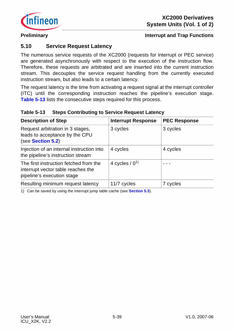
XC2000 DerivativesSystem Units (Vol. 1 of 2)
Interrupt and Trap FunctionsPreliminary
5.10 Service Request Latency The numerous service requests of the XC2000 (requests for interrupt or PEC service)are generated asynchronously with respect to the execution of the instruction flow.Therefore, these requests are arbitrated and are inserted into the current instructionstream. This decouples the service request handling from the currently executedinstruction stream, but also leads to a certain latency.The request latency is the time from activating a request signal at the interrupt controller(ITC) until the corresponding instruction reaches the pipeline’s execution stage.Table 5-13 lists the consecutive steps required for this process.
Table 5-13 Steps Contributing to Service Request LatencyDescription of Step Interrupt Response PEC ResponseRequest arbitration in 3 stages,leads to acceptance by the CPU(see Section 5.2)
3 cycles 3 cycles
Injection of an internal instruction into the pipeline’s instruction stream
4 cycles 4 cycles
The first instruction fetched from the interrupt vector table reaches the pipeline’s execution stage
4 cycles / 01)
1) Can be saved by using the interrupt jump table cache (see Section 5.3).
- - -
Resulting minimum request latency 11/7 cycles 7 cycles
User’s Manual 5-39 V1.0, 2007-06ICU_X2K, V2.2
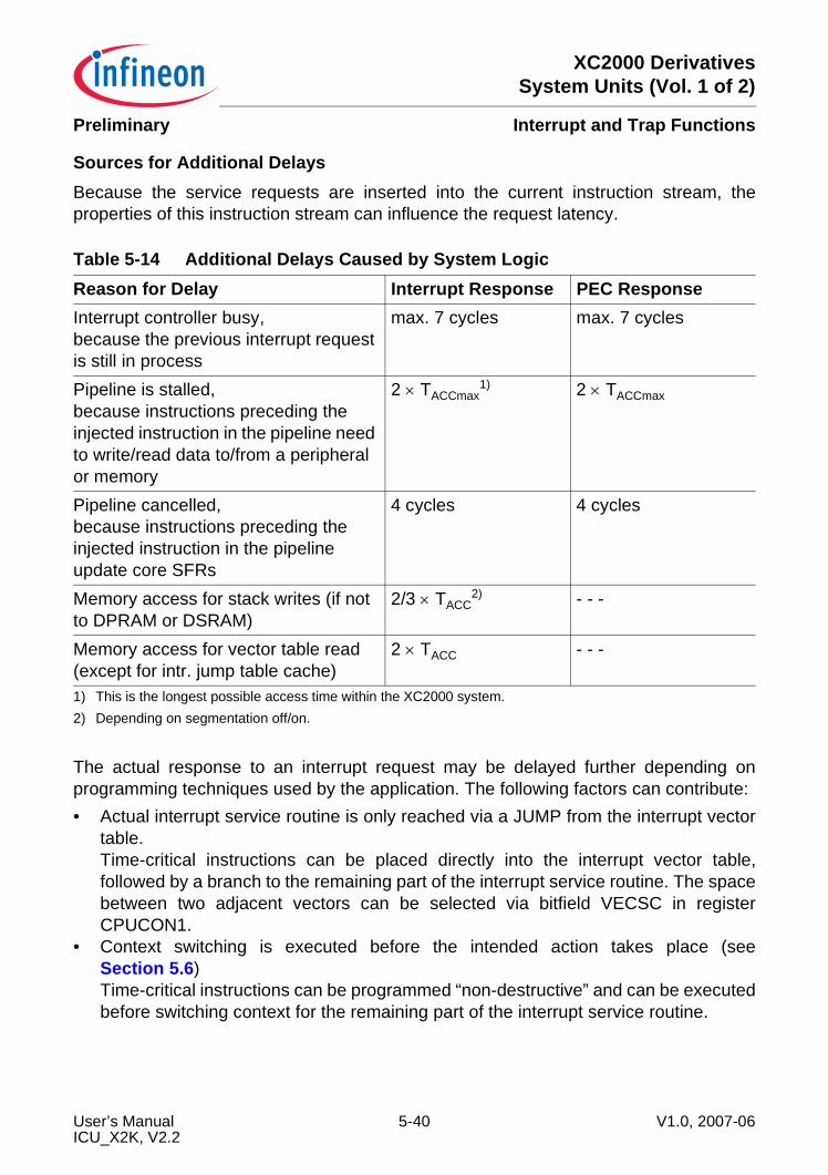
XC2000 DerivativesSystem Units (Vol. 1 of 2)
Interrupt and Trap FunctionsPreliminary
Sources for Additional DelaysBecause the service requests are inserted into the current instruction stream, theproperties of this instruction stream can influence the request latency.
The actual response to an interrupt request may be delayed further depending onprogramming techniques used by the application. The following factors can contribute:• Actual interrupt service routine is only reached via a JUMP from the interrupt vector
table.Time-critical instructions can be placed directly into the interrupt vector table,followed by a branch to the remaining part of the interrupt service routine. The spacebetween two adjacent vectors can be selected via bitfield VECSC in registerCPUCON1.
• Context switching is executed before the intended action takes place (seeSection 5.6)Time-critical instructions can be programmed “non-destructive” and can be executedbefore switching context for the remaining part of the interrupt service routine.
Table 5-14 Additional Delays Caused by System LogicReason for Delay Interrupt Response PEC ResponseInterrupt controller busy,because the previous interrupt request is still in process
max. 7 cycles max. 7 cycles
Pipeline is stalled,because instructions preceding the injected instruction in the pipeline need to write/read data to/from a peripheral or memory
2 × TACCmax1)
1) This is the longest possible access time within the XC2000 system.
2 × TACCmax
Pipeline cancelled,because instructions preceding the injected instruction in the pipeline update core SFRs
4 cycles 4 cycles
Memory access for stack writes (if not to DPRAM or DSRAM)
2/3 × TACC2)
2) Depending on segmentation off/on.
- - -
Memory access for vector table read(except for intr. jump table cache)
2 × TACC - - -
User’s Manual 5-40 V1.0, 2007-06ICU_X2K, V2.2
XC2000 DerivativesSystem Units (Vol. 1 of 2)
Interrupt and Trap FunctionsPreliminary
5.11 Trap Functions Traps interrupt current execution in a manner similar to standard interrupts. However,trap functions offer the possibility to bypass the interrupt system’s prioritization processfor cases in which immediate system reaction is required. Trap functions are notmaskable and always have priority over interrupt requests on any priority level.The XC2000 provides two different kinds of trapping mechanisms: Hardware Traps aretriggered by events that occur during program execution (such as illegal access orundefined opcode); Software Traps are initiated via an instruction within the currentexecution flow.
Software Traps The TRAP instruction causes a software call to an interrupt service routine. The vectornumber specified in the operand field of the trap instruction determines which vectorlocation in the vector table will be branched to.Executing a TRAP instruction causes an effect similar to the occurrence of an interruptat the same vector. PSW, CSP (in segmentation mode), and IP are pushed on theinternal system stack and a jump is taken to the specified vector location. When a trapis executed, the CSP for the trap service routine is loaded from register VECSEG. NoInterrupt Request flags are affected by the TRAP instruction. The interrupt serviceroutine called by a TRAP instruction must be terminated with a RETI (return frominterrupt) instruction to ensure correct operation.Note: The CPU priority level and the selected register bank in register PSW are not
modified by the TRAP instruction, so the service routine is executed on the samepriority level from which it was invoked. Therefore, the service routine entered bythe TRAP instruction uses the original register bank and can be interrupted byother traps or higher priority interrupts, other than when triggered by a hardwareevent.
Hardware Traps Hardware traps are issued by faults or specific system states which occur during runtimeof a program (not identified at assembly time). A hardware trap may also be triggeredintentionally, for example: to emulate additional instructions by generating an IllegalOpcode trap. The XC2000 distinguishes nine different hardware trap functions. When ahardware trap condition has been detected, the CPU branches to the trap vector locationfor the respective trap condition. The instruction which caused the trap is completedbefore the trap handling routine is entered.Hardware traps are non-maskable and always have priority over every other CPUactivity. If several hardware trap conditions are detected within the same instructioncycle, the highest priority trap is serviced (see Table 5-3).
User’s Manual 5-41 V1.0, 2007-06ICU_X2K, V2.2
XC2000 DerivativesSystem Units (Vol. 1 of 2)
Interrupt and Trap FunctionsPreliminary
PSW, CSP (in segmentation mode), and IP are pushed on the internal system stack andthe CPU level in register PSW is set to the highest possible priority level (level 15),disabling all interrupts. The global register bank is selected. Execution branches to therespective trap vector in the vector table. A trap service routine must be terminated withthe RETI instruction.The nine hardware trap functions of the XC2000 are divided into two classes:Class A traps are:• System Request 0 (SR0)• Stack Overflow• Stack Underflow trap• Software BreakThese traps share the same trap priority, but have individual vector addresses.Class B traps are:• System Request 1 (SR1)• Undefined Opcode• Memory Access Error• Protection Fault• Illegal Word Operand AccessThe Class B traps share the same trap priority and the same vector address.The bit-addressable Trap Flag Register (TFR) allows a trap service routine to identify thekind of trap which caused the exception. Each trap function is indicated by a separaterequest flag. When a hardware trap occurs, the corresponding request flag in registerTFR is set to ‘1’.The reset functions may be regarded as a type of trap. Reset functions have the highestsystem priority (trap priority III).Class A traps have the second highest priority (trap priority II), on the 3rd rank areClass B traps, so a Class A trap can interrupt a Class B trap. If more than one Class Atrap occur at a time, they are prioritized internally, with the SR0 trap at the highest andthe software break trap at the lowest priority.In the case where e.g. an Undefined Opcode trap (class B) occurs simultaneously withan SR0 trap (class A), both the SR0 and the UNDOPC flag is set, the IP of the instructionwith the undefined opcode is pushed onto the system stack, but the SR0 trap isexecuted. After return from the SR0 service routine, the IP is popped from the stack andimmediately pushed again because of the pending UNDOPC trap.Note: The trap service routine must clear the respective trap flag; otherwise, a new trap
will be requested after exiting the service routine. Setting a trap request flag bysoftware causes the same effects as if it had been set by hardware.
User’s Manual 5-42 V1.0, 2007-06ICU_X2K, V2.2
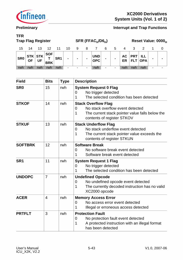
XC2000 DerivativesSystem Units (Vol. 1 of 2)
Interrupt and Trap FunctionsPreliminary
TFR Trap Flag Register SFR (FFACH/D6H) Reset Value: 0000H
15 14 13 12 11 10 9 8 7 6 5 4 3 2 1 0
SR0 STK OF
STK UF
SOFT
BRKSR1 - - - UND
OPC - - AC ER
PRT FLT
ILL OPA - -
rwh rwh rwh rwh rwh - - - rwh - - rwh rwh rwh - -
Field Bits Type DescriptionSR0 15 rwh System Request 0 Flag
0 No trigger detected1 The selected condition has been detected
STKOF 14 rwh Stack Overflow Flag0 No stack overflow event detected1 The current stack pointer value falls below the
contents of register STKOVSTKUF 13 rwh Stack Underflow Flag
0 No stack underflow event detected1 The current stack pointer value exceeds the
contents of register STKUNSOFTBRK 12 rwh Software Break
0 No software break event detected1 Software break event detected
SR1 11 rwh System Request 1 Flag0 No trigger detected1 The selected condition has been detected
UNDOPC 7 rwh Undefined Opcode0 No undefined opcode event detected1 The currently decoded instruction has no valid
XC2000 opcodeACER 4 rwh Memory Access Error
0 No access error event detected1 Illegal or erroneous access detected
PRTFLT 3 rwh Protection Fault0 No protection fault event detected1 A protected instruction with an illegal format
has been detected
User’s Manual 5-43 V1.0, 2007-06ICU_X2K, V2.2
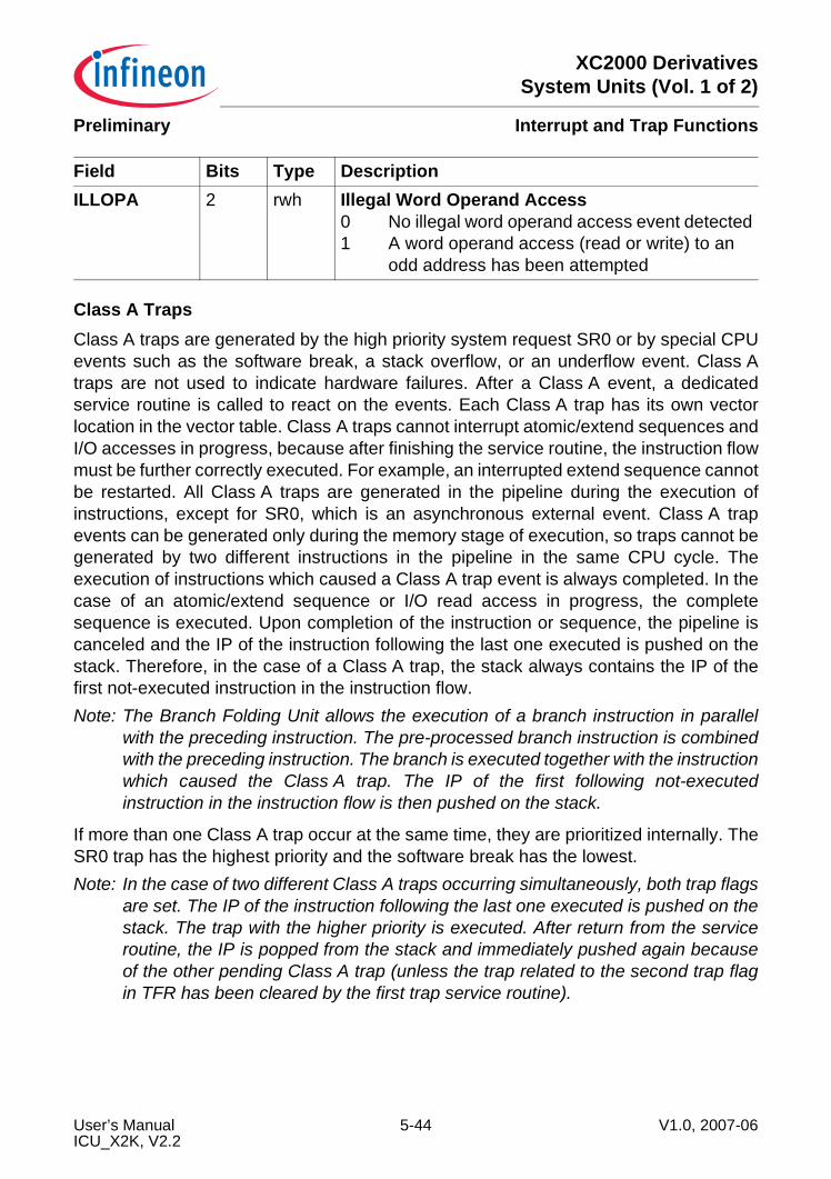
XC2000 DerivativesSystem Units (Vol. 1 of 2)
Interrupt and Trap FunctionsPreliminary
Class A TrapsClass A traps are generated by the high priority system request SR0 or by special CPUevents such as the software break, a stack overflow, or an underflow event. Class Atraps are not used to indicate hardware failures. After a Class A event, a dedicatedservice routine is called to react on the events. Each Class A trap has its own vectorlocation in the vector table. Class A traps cannot interrupt atomic/extend sequences andI/O accesses in progress, because after finishing the service routine, the instruction flowmust be further correctly executed. For example, an interrupted extend sequence cannotbe restarted. All Class A traps are generated in the pipeline during the execution ofinstructions, except for SR0, which is an asynchronous external event. Class A trapevents can be generated only during the memory stage of execution, so traps cannot begenerated by two different instructions in the pipeline in the same CPU cycle. Theexecution of instructions which caused a Class A trap event is always completed. In thecase of an atomic/extend sequence or I/O read access in progress, the completesequence is executed. Upon completion of the instruction or sequence, the pipeline iscanceled and the IP of the instruction following the last one executed is pushed on thestack. Therefore, in the case of a Class A trap, the stack always contains the IP of thefirst not-executed instruction in the instruction flow.Note: The Branch Folding Unit allows the execution of a branch instruction in parallel
with the preceding instruction. The pre-processed branch instruction is combinedwith the preceding instruction. The branch is executed together with the instructionwhich caused the Class A trap. The IP of the first following not-executedinstruction in the instruction flow is then pushed on the stack.
If more than one Class A trap occur at the same time, they are prioritized internally. TheSR0 trap has the highest priority and the software break has the lowest.Note: In the case of two different Class A traps occurring simultaneously, both trap flags
are set. The IP of the instruction following the last one executed is pushed on thestack. The trap with the higher priority is executed. After return from the serviceroutine, the IP is popped from the stack and immediately pushed again becauseof the other pending Class A trap (unless the trap related to the second trap flagin TFR has been cleared by the first trap service routine).
ILLOPA 2 rwh Illegal Word Operand Access0 No illegal word operand access event detected1 A word operand access (read or write) to an
odd address has been attempted
Field Bits Type Description
User’s Manual 5-44 V1.0, 2007-06ICU_X2K, V2.2
XC2000 DerivativesSystem Units (Vol. 1 of 2)
Interrupt and Trap FunctionsPreliminary
Class B TrapsClass B traps are generated by unrecoverable hardware failures. In the case of ahardware failure, the CPU must immediately start a failure service routine. Class B trapscan interrupt an atomic/extend sequence and an I/O read access. After finishing theClass B service routine, a restoration of the interrupted instruction flow is not possible.All Class B traps have the same priority (trap priority I). When several Class B trapsbecome active at the same time, the corresponding flags in the TFR register are set andthe trap service routine is entered. Because all Class B traps have the same vector, thepriority of service of simultaneously occurring Class B traps is determined by software inthe trap service routine.The access error (ACER) and system request 1 (SR1) are asynchronous external (to theCPU) events, while all other Class B traps are generated in the pipeline during theexecution of instructions. Class B trap events can be generated only during the memorystage of execution, so traps cannot be generated by two different instructions in thepipeline in the same CPU cycle. Instructions which caused a Class B trap event arealways executed, then the pipeline is canceled and the IP of the instruction following theone which caused the trap is pushed on the stack. Therefore, the stack always containsthe IP of the first following not-executed instruction in the instruction flow.Note: The Branch Folding Unit allows the execution of a branch instruction in parallel
with the preceding instruction. The pre-processed branch instruction is combinedwith the preceding instruction. The branch is executed together with the instructioncausing the Class B trap. The IP of the first following not-executed instruction inthe instruction flow is pushed on the stack.
A Class A trap occurring during the execution of a Class B trap service routine will beserviced immediately. During the execution of a Class A trap service routine, however,any Class B trap occurring will not be serviced until the Class A trap service routine isexited with a RETI instruction. In this case, the occurrence of the Class B trap conditionis stored in the TFR register, but the IP value of the instruction which caused this trap islost.Note: If a Class A trap occurs simultaneously with a Class B trap, both trap flags are set.
The IP of the instruction following the one which caused the trap is pushed into thestack, and the Class A trap is executed. If this occurs during execution of anatomic/extend sequence or I/O read access in progress, then the presence of theClass B trap breaks the protection of atomic/extend operations and the Class Atrap will be executed immediately without waiting for the sequence completion.After return from the service routine, the IP is popped from the system stack andimmediately pushed again because of the other pending Class B trap. In thissituation, the restoration of the interrupted instruction flow is not possible.
User’s Manual 5-45 V1.0, 2007-06ICU_X2K, V2.2
XC2000 DerivativesSystem Units (Vol. 1 of 2)
Interrupt and Trap FunctionsPreliminary
System Request 0 Trap (A)Whenever a high-to-low transition on the respective CPU-input is detected (i.e. thedefined condition has become true), the SR0 flag in register TFR is set and the CPU willenter the SR0 trap routine.
Stack Overflow Trap (A)Whenever the stack pointer is implicitly decremented and the stack pointer is equal tothe value in the stack overflow register STKOV, the STKOF flag in register TFR is setand the CPU will enter the stack overflow trap routine.For recovery from stack overflow, it must be ensured that there is enough excess spaceon the stack to save the current system state twice (PSW, IP, in segmented mode alsoCSP). Otherwise, a system reset should be generated.
Stack Underflow Trap (A)Whenever the stack pointer is implicitly incremented and the stack pointer is equal to thevalue in the stack underflow register STKUN, the STKUF flag is set in register TFR andthe CPU will enter the stack underflow trap routine.
Software Break Trap (A)When the instruction currently being executed by the CPU is a SBRK instruction, theSOFTBRK flag is set in register TFR and the CPU enters the software break debugroutine. The flag generation of the software break instruction can be disabled by the On-chip Emulation Module. In this case, the instruction only breaks the instruction flow andsignals this event to the debugger, the flag is not set and the trap will not be executed.
System Request 1 Trap (B)Whenever a high-to-low transition on the respective CPU-input is detected (i.e. thedefined condition has become true), the SR1 flag in register TFR is set and the CPU willenter the SR1 trap routine.
Undefined Opcode Trap (B)When the instruction currently decoded by the CPU does not contain a valid XC2000opcode, the UNDOPC flag is set in register TFR and the CPU enters the undefinedopcode trap routine. The instruction that causes the undefined opcode trap is executedas a NOP.This can be used to emulate unimplemented instructions. The trap service routine canexamine the faulting instruction to decode operands for unimplemented opcodes basedon the stacked IP. In order to resume processing, the stacked IP value must beincremented by the size of the undefined instruction, which is determined by the user,before a RETI instruction is executed.
User’s Manual 5-46 V1.0, 2007-06ICU_X2K, V2.2
XC2000 DerivativesSystem Units (Vol. 1 of 2)
Interrupt and Trap FunctionsPreliminary
Memory Access Error (B)When a memory access error is detected, the ACER flag is set in register TFR and theCPU enters the access error trap routine. The access error is reported in the followingcases:• access to Flash memory while it is disabled• access to Flash memory from outside while read-protection is active• double bit error detected when reading Flash memory• access to reserved locations (see memory map in Table 3-1)• parity error during an access to RAMIn case of an access error, additionally the soft-trap code 1E9BH is issued.
Protection Fault Trap (B)Whenever one of the special protected instructions is executed where the opcode of thatinstruction is not repeated twice in the second word of the instruction and the bytefollowing the opcode is not the complement of the opcode, the PRTFLT flag in registerTFR is set and the CPU enters the protection fault trap routine. The protectedinstructions include DISWDT, EINIT, IDLE, PWRDN, SRST, ENWDT and SRVWDT.The instruction that causes the protection fault trap is executed like a NOP.
Illegal Word Operand Access Trap (B)Whenever a word operand read or write access is attempted to an odd byte address, theILLOPA flag in register TFR is set and the CPU enters the illegal word operand accesstrap routine.
User’s Manual 5-47 V1.0, 2007-06ICU_X2K, V2.2
XC2000 DerivativesSystem Units (Vol. 1 of 2)
Interrupt and Trap FunctionsPreliminary
User’s Manual 5-48 V1.0, 2007-06ICU_X2K, V2.2
XC2000 DerivativesSystem Units (Vol. 1 of 2)
System Control Unit (SCU)Preliminary
6 System Control Unit (SCU)The System Control Unit (SCU) of the XC2000 handles all system control tasks besidethe debug related tasks which are controlled by the OCDS/Cerberus and the test relatedtasks which are controlled by the TCU. All functions described in this chapter are tightlycoupled, thus, they are conveniently handled by one unit, the SCU.The SCU contains the following functional sub-blocks:• Clock Generation (see Section 6.1 on Page 6-2)• Reset Operation (see Section 6.2 on Page 6-33)• Power Supply (see Section 6.5 on Page 6-90)• Global State Control (see Section 6.6 on Page 6-156)• Wake-up Timer (see Section 6.9 on Page 6-176)• Register Access Control (see Section 6.10.1 on Page 6-181)• Watchdog Timer (see Section 6.8 on Page 6-168)• External Interrupts (see Section 6.4 on Page 6-64)• Temperature Compensation (see Section 6.7 on Page 6-165)• SCU registers and Address map (see Section 6.13 on Page 6-220)
User’s Manual 6-1 V1.0, 2007-06SCU, V1.1
XC2000 DerivativesSystem Units (Vol. 1 of 2)
System Control Unit (SCU)Preliminary
6.1 Clock Generation UnitThe Clock Generation Unit (CGU) allows a very flexible clock generation for XC2000.During user program execution the frequency can be programmed for an optimal ratiobetween performance and power consumption. Therefore the power consumption canbe adapted to the actual application state.The CGU in the XC2000 consists of a clock generator block and a clock control unit(CCU). The CGU can convert a low-frequency external clock to a high-speed internalclock, or can create a high-speed internal clock without external input.The system clock fSYS is generated out of four selectable clocks:• PLL clock fPLL• Wake-Up clock fWU• The Direct Clock fOSC, from pin XTAL1• Input DIRIN as Direct Clock Input fDIR
The RTC clock fRTC which is generated out of four selectable clocks:• PLL clock fPLL• The Direct Clock from pin XTAL1 fOSC• Input DIRIN as Direct Clock Input fDIR• Input DRTC as Direct Clock Input fDRTC
Figure 6-1 Clock Generation Unit Block Diagram
CGU_Block_Diagram.vsd
Clock Generation Unit (CGU)
CCU
Clock Generator
fOSC
fWU
fDIRIN
fPDRTC
XTAL1
XTAL2
DIRIN
DRTC
fSYS
to RTC
EXTCLK
to CC60
fPLL
fRTC
fSYS
User’s Manual 6-2 V1.0, 2007-06SCU, V1.1
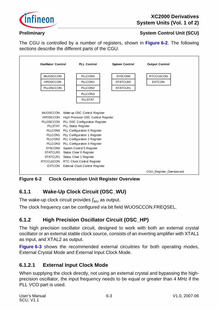
XC2000 DerivativesSystem Units (Vol. 1 of 2)
System Control Unit (SCU)Preliminary
The CGU is controlled by a number of registers, shown in Figure 6-2. The followingsections describe the different parts of the CGU.
Figure 6-2 Clock Generation Unit Register Overview
6.1.1 Wake-Up Clock Circuit (OSC_WU)The wake-up clock circuit provides fWU as output.The clock frequency can be configured via bit field WUOSCCON.FREQSEL.
6.1.2 High Precision Oscillator Circuit (OSC_HP)The high precision oscillator circuit, designed to work with both an external crystaloscillator or an external stable clock source, consists of an inverting amplifier with XTAL1as input, and XTAL2 as output.Figure 6-3 shows the recommended external circuitries for both operating modes,External Crystal Mode and External Input Clock Mode.
6.1.2.1 External Input Clock ModeWhen supplying the clock directly, not using an external crystal and bypassing the high-precision oscillator, the input frequency needs to be equal or greater than 4 MHz if thePLL VCO part is used.
CGU_Register_Overview.vsd
Output ControlOscillator Control System Control
PLLCON2PLLCON3SYSCON0
WUOSCCON
HPOSCCON
PLLOSCCON
PLLSTAT
PLLCON0
PLLCON1
PLLCON2
PLLCON3
SYSCON0
STATCLR0
STATCLR1
RTCCLKCON
EXTCON
STATCLR0STATCLR1
RTCCLKCON
PLL Configuration 2 RegisterPLL Configuration 3 RegisterSystem Control 0 RegisterStatus Clear 0 RegisterStatus Clear 1 RegisterRTC Clock Control Register
EXTCON External Clock Control Register
WUOSCCONHPOSCCONPLLOSCCON
PLLSTATPLLCON0PLLCON1
Wake-up OSC Control RegisterHigh Precision OSC Control RegisterPLL OSC Configuration RegisterPLL Status RegisterPLL Configuration 0 RegisterPLL Configuration 1 Register
PLL Control
User’s Manual 6-3 V1.0, 2007-06SCU, V1.1
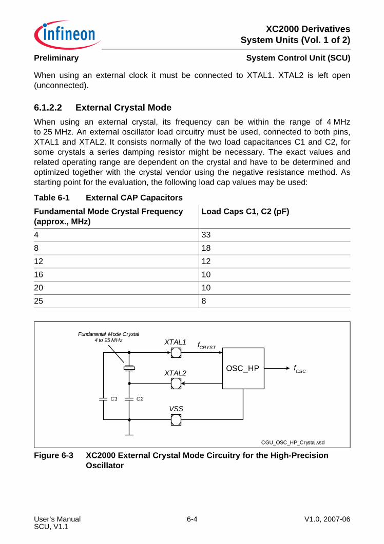
XC2000 DerivativesSystem Units (Vol. 1 of 2)
System Control Unit (SCU)Preliminary
When using an external clock it must be connected to XTAL1. XTAL2 is left open(unconnected).
6.1.2.2 External Crystal ModeWhen using an external crystal, its frequency can be within the range of 4 MHzto 25 MHz. An external oscillator load circuitry must be used, connected to both pins,XTAL1 and XTAL2. It consists normally of the two load capacitances C1 and C2, forsome crystals a series damping resistor might be necessary. The exact values andrelated operating range are dependent on the crystal and have to be determined andoptimized together with the crystal vendor using the negative resistance method. Asstarting point for the evaluation, the following load cap values may be used:
Figure 6-3 XC2000 External Crystal Mode Circuitry for the High-Precision Oscillator
Table 6-1 External CAP CapacitorsFundamental Mode Crystal Frequency (approx., MHz)
Load Caps C1, C2 (pF)
4 338 1812 1216 1020 1025 8
CGU_OSC_HP_Crystal.vsd
OSC_HP fOSC
XTAL1
XTAL2
C1 C2
VSS
fCRYST
Fundamental Mode Crystal4 to 25 MHz
User’s Manual 6-4 V1.0, 2007-06SCU, V1.1
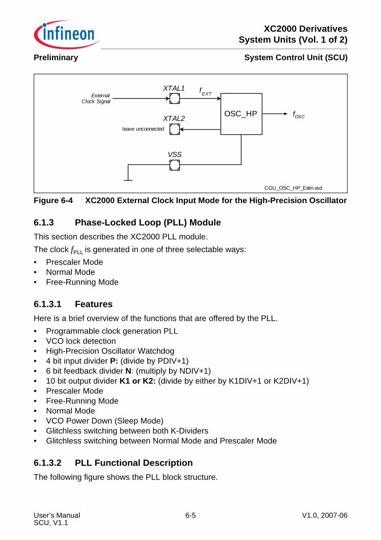
XC2000 DerivativesSystem Units (Vol. 1 of 2)
System Control Unit (SCU)Preliminary
Figure 6-4 XC2000 External Clock Input Mode for the High-Precision Oscillator
6.1.3 Phase-Locked Loop (PLL) ModuleThis section describes the XC2000 PLL module.The clock fPLL is generated in one of three selectable ways:• Prescaler Mode• Normal Mode• Free-Running Mode
6.1.3.1 FeaturesHere is a brief overview of the functions that are offered by the PLL.• Programmable clock generation PLL• VCO lock detection• High-Precision Oscillator Watchdog• 4 bit input divider P: (divide by PDIV+1)• 6 bit feedback divider N: (multiply by NDIV+1)• 10 bit output divider K1 or K2: (divide by either by K1DIV+1 or K2DIV+1)• Prescaler Mode• Free-Running Mode• Normal Mode• VCO Power Down (Sleep Mode)• Glitchless switching between both K-Dividers• Glitchless switching between Normal Mode and Prescaler Mode
6.1.3.2 PLL Functional DescriptionThe following figure shows the PLL block structure.
CGU_OSC_HP_ExtIn.vsd
OSC_HP fOSC
XTAL1
XTAL2
VSS
fEXTExternalClock Signal
leave unconnected
User’s Manual 6-5 V1.0, 2007-06SCU, V1.1
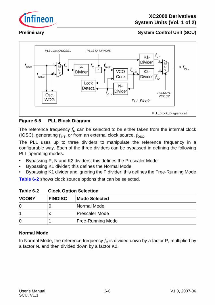
XC2000 DerivativesSystem Units (Vol. 1 of 2)
System Control Unit (SCU)Preliminary
Figure 6-5 PLL Block Diagram
The reference frequency fR can be selected to be either taken from the internal clock(IOSC), generating fINT, or from an external clock source, fOSC.The PLL uses up to three dividers to manipulate the reference frequency in aconfigurable way. Each of the three dividers can be bypassed in defining the followingPLL operating modes.• Bypassing P, N and K2 dividers; this defines the Prescaler Mode• Bypassing K1 divider; this defines the Normal Mode• Bypassing K1 divider and ignoring the P divider; this defines the Free-Running ModeTable 6-2 shows clock source options that can be selected.
Normal ModeIn Normal Mode, the reference frequency fR is divided down by a factor P, multiplied bya factor N, and then divided down by a factor K2.
Table 6-2 Clock Option SelectionVCOBY FINDISC Mode Selected0 0 Normal Mode1 x Prescaler Mode0 1 Free-Running Mode
PLL_Block_Diagram.vsd
PLL Block
fOSC
Osc.WDG
P-Divider VCO
CoreK2-
Divider
N-Divider
LockDetect.
K1-Divider
fPLL
fK2
fK1
fVCO
fDIV
fREFfPfR
PLLCON.OSCSEL PLLSTAT.FINDIS
PLLCON.VCOBY
MUX
MUX1
0
0
1
fIOSC
User’s Manual 6-6 V1.0, 2007-06SCU, V1.1
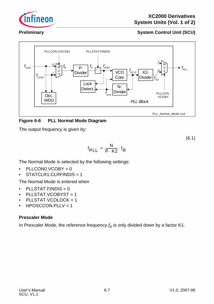
XC2000 DerivativesSystem Units (Vol. 1 of 2)
System Control Unit (SCU)Preliminary
Figure 6-6 PLL Normal Mode Diagram
The output frequency is given by:
(6.1)
The Normal Mode is selected by the following settings:• PLLCON0.VCOBY = 0• STATCLR1.CLRFINDIS = 1The Normal Mode is entered when• PLLSTAT.FINDIS = 0• PLLSTAT.VCOBYST = 1• PLLSTAT.VCOLOCK = 1• HPOSCCON.PLLV = 1
Prescaler ModeIn Prescaler Mode, the reference frequency fR is only divided down by a factor K1.
PLL_Normal_Mode.vsd
PLL Block
fOSC
Osc.WDG
P-Divider VCO
CoreK2-
Divider
N-Divider
LockDetect.
fPLL
fK2
fVCO
fDIV
fREFfPfR
PLLCON.OSCSEL PLLSTAT.FINDIS
PLLCON.VCOBY
MUX
MUX1
0
0
1
fIOSC
fPLLN
P K2⋅---------------- fR⋅=
User’s Manual 6-7 V1.0, 2007-06SCU, V1.1
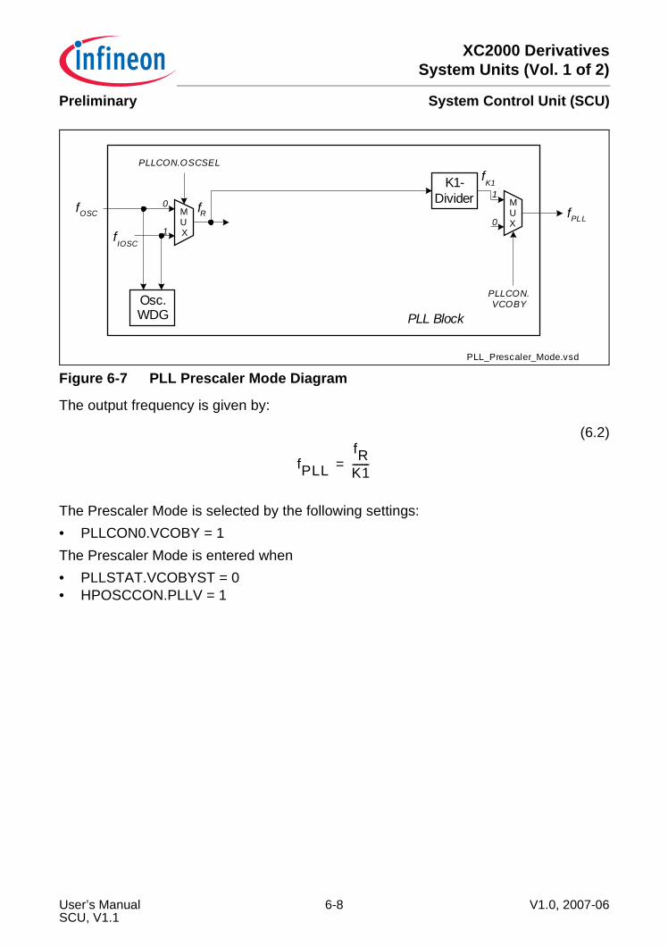
XC2000 DerivativesSystem Units (Vol. 1 of 2)
System Control Unit (SCU)Preliminary
Figure 6-7 PLL Prescaler Mode Diagram
The output frequency is given by:
(6.2)
The Prescaler Mode is selected by the following settings:• PLLCON0.VCOBY = 1The Prescaler Mode is entered when • PLLSTAT.VCOBYST = 0• HPOSCCON.PLLV = 1
PLL_Prescaler_Mode.vsd
PLL Block
fOSC
Osc.WDG
K1-Divider
fPLL
fK1
fR
PLLCON.OSCSEL
PLLCON.VCOBY
MUX
MUX1
0
0
1
fIOSC
fPLLfRK1-------=
User’s Manual 6-8 V1.0, 2007-06SCU, V1.1
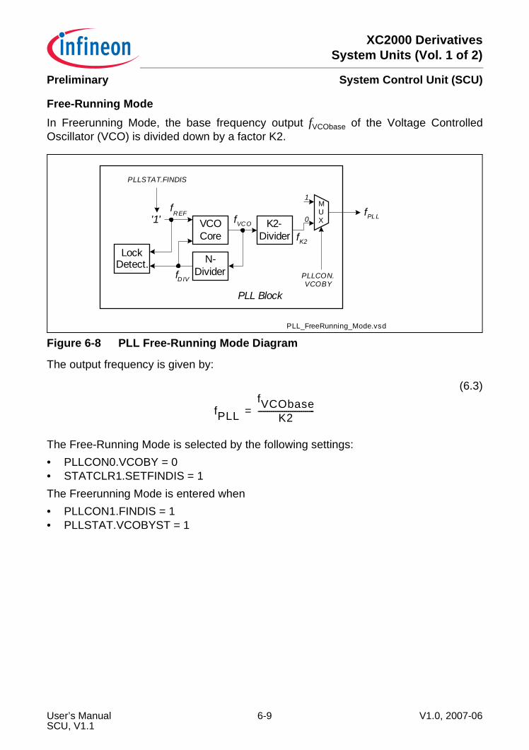
XC2000 DerivativesSystem Units (Vol. 1 of 2)
System Control Unit (SCU)Preliminary
Free-Running ModeIn Freerunning Mode, the base frequency output fVCObase of the Voltage ControlledOscillator (VCO) is divided down by a factor K2.
Figure 6-8 PLL Free-Running Mode Diagram
The output frequency is given by:
(6.3)
The Free-Running Mode is selected by the following settings:• PLLCON0.VCOBY = 0• STATCLR1.SETFINDIS = 1The Freerunning Mode is entered when • PLLCON1.FINDIS = 1• PLLSTAT.VCOBYST = 1
PLL_FreeRunning_Mode.vsd
PLL Block
VCOCore
K2-Divider
N-Divider
LockDetect.
fPLL
fK2
fVCO
fDIV
fREF
PLLCON.VCOBY
MUX0
1
PLLSTAT.FINDIS
'1'
fPLLfVCObase
K2------------------------------=
User’s Manual 6-9 V1.0, 2007-06SCU, V1.1
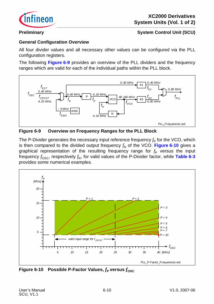
XC2000 DerivativesSystem Units (Vol. 1 of 2)
System Control Unit (SCU)Preliminary
General Configuration OverviewAll four divider values and all necessary other values can be configured via the PLLconfiguration registers.The following Figure 6-9 provides an overview of the PLL dividers and the frequencyranges which are valid for each of the individual paths within the PLL block.
Figure 6-9 Overview on Frequency Ranges for the PLL Block
The P-Divider generates the necessary input reference frequency fP for the VCO, whichis then compared to the divided output frequency fN of the VCO. Figure 6-10 gives agraphical representation of the resulting frequency range for fP versus the inputfrequency fOSC, respectively fR, for valid values of the P-Divider factor, while Table 6-3provides some numerical examples.
Figure 6-10 Possible P-Factor Values, fP versus fOSC
PLL_Frequencies.vsd
IOSC
fOSC PVCO K2
N
K1
fPLL
0..80 MHz
0..40 MHz 0..40 MHz
0..80 MHz
4..16 MHz
4..16 MHz
4..40 MHz
~ 5 MHz
48..160 MHz
0..40 MHz
4..25 MHz
fEXT
fCRYST fPfN
fVCO
fK1
fK2fR
fIOSC
PLL_P-Factor_Frequencies.vsd
P = 1 P = 2
P = 3
P = 4
P = 5P = 6P = 7P = 10
fOSC
fP
[MHz]
[MHz]
5 10 15 20 25 30 35 40
5
10
15
20
valid input range for fCRYST
User’s Manual 6-10 V1.0, 2007-06SCU, V1.1
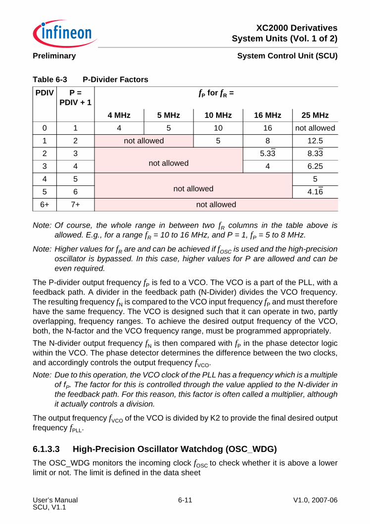
XC2000 DerivativesSystem Units (Vol. 1 of 2)
System Control Unit (SCU)Preliminary
Note: Of course, the whole range in between two fR columns in the table above isallowed. E.g., for a range fR = 10 to 16 MHz, and P = 1, fP = 5 to 8 MHz.
Note: Higher values for fR are and can be achieved if fOSC is used and the high-precisionoscillator is bypassed. In this case, higher values for P are allowed and can beeven required.
The P-divider output frequency fP is fed to a VCO. The VCO is a part of the PLL, with afeedback path. A divider in the feedback path (N-Divider) divides the VCO frequency.The resulting frequency fN is compared to the VCO input frequency fP and must thereforehave the same frequency. The VCO is designed such that it can operate in two, partlyoverlapping, frequency ranges. To achieve the desired output frequency of the VCO,both, the N-factor and the VCO frequency range, must be programmed appropriately.The N-divider output frequency fN is then compared with fP in the phase detector logicwithin the VCO. The phase detector determines the difference between the two clocks,and accordingly controls the output frequency fVCO.Note: Due to this operation, the VCO clock of the PLL has a frequency which is a multiple
of fP. The factor for this is controlled through the value applied to the N-divider inthe feedback path. For this reason, this factor is often called a multiplier, althoughit actually controls a division.
The output frequency fVCO of the VCO is divided by K2 to provide the final desired outputfrequency fPLL.
6.1.3.3 High-Precision Oscillator Watchdog (OSC_WDG)The OSC_WDG monitors the incoming clock fOSC to check whether it is above a lowerlimit or not. The limit is defined in the data sheet
Table 6-3 P-Divider FactorsPDIV P =
PDIV + 1fP for fR =
4 MHz 5 MHz 10 MHz 16 MHz 25 MHz0 1 4 5 10 16 not allowed1 2 not allowed 5 8 12.52 3
not allowed5.33 8.33
3 4 4 6.254 5
not allowed5
5 6 4.166+ 7+ not allowed
User’s Manual 6-11 V1.0, 2007-06SCU, V1.1
XC2000 DerivativesSystem Units (Vol. 1 of 2)
System Control Unit (SCU)Preliminary
The OSC_WDG uses the internal clock (IOSC) frequency fIOSC for its operation, thus, theinternal clock has to be enabled.By setting bit HPOSCCON.OSCWDTRST, the detection can be restarted without a resetof the complete PLL, e.g., in case of OSC loss-of-lock condition.Note: After the OSC_WDG is reset, bit HPOSCCON.PLLV is not valid for some time
(544 * fOSCPLL).
6.1.3.4 PLL VCO Lock DetectionThe PLL has a lock detection, which supervises the VCO part of the PLL in order todifferentiate between stable and instable VCO circuit behavior. The lock detector marksthe VCO output fVCO as instable, if the two inputs, fP and fR, differ too much. Changes inone or both input frequencies below a certain deviation are not marked as a loss of lock,since the VCO can handle such small changes without any problem for the system.
6.1.3.5 Internal Clock (OSC_PLL)The PLL internal clock can be used for two different applications:
Operating the OSC_WDGWith this option, the input frequency for the PLL, either from OSC_HP or from XTAL1, issupervised with OSC_PLL. For more information, please see Chapter 6.1.3.3.
Providing an input clock to the PLLIn case no external clock input is used via XTAL1, the clock frequency fIOSC of the internalPLL clock, IOSC, can be used as input clock for all PLL modes. This is controlled andconfigured via PLLCON1.OSCSEL.
6.1.3.6 Switching PLL ParametersThe following restrictions apply when changing PLL parameters via the PLLCON0through PLLCON3 registers:• The VCO bypass switch may be used at any time, however, it has to be ensured that
the maximum operating frequency of the device (see data sheet) will not beexceeded.
• Before switching NDIV and PDIV, the Prescaler Mode has to be selected. • Before deselecting the Prescaler Mode, the RESLD bit has to be set and then the
VCOLOCK flag has to be checked. Only when the VCOLOCK flag is set again, thePrescaler Mode may be deselected.
• Before changing VCOSEL, the Prescaler Mode must be selected.Note: PDIV and NDIV can also be switched in Normal Mode. When changing NDIV, it
must be regarded that the VCO clock fVCO may exceed the target frequency until
User’s Manual 6-12 V1.0, 2007-06SCU, V1.1
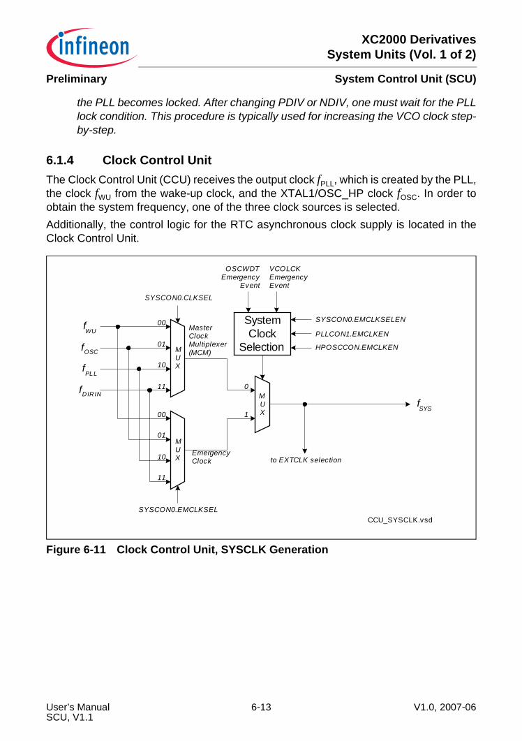
XC2000 DerivativesSystem Units (Vol. 1 of 2)
System Control Unit (SCU)Preliminary
the PLL becomes locked. After changing PDIV or NDIV, one must wait for the PLLlock condition. This procedure is typically used for increasing the VCO clock step-by-step.
6.1.4 Clock Control UnitThe Clock Control Unit (CCU) receives the output clock fPLL, which is created by the PLL,the clock fWU from the wake-up clock, and the XTAL1/OSC_HP clock fOSC. In order toobtain the system frequency, one of the three clock sources is selected.Additionally, the control logic for the RTC asynchronous clock supply is located in theClock Control Unit.
Figure 6-11 Clock Control Unit, SYSCLK Generation
CCU_SYSCLK.vsd
fWU
fOSC
fPLL
MUX
00
01
10
11
MUX
00
01
10
11
MUX
0
1
SystemClock
Selection
fSYS
SYSCON0.CLKSEL
SYSCON0.EMCLKSEL
SYSCON0.EMCLKSELEN
PLLCON1.EMCLKEN
HPOSCCON.EMCLKEN
OSCWDTEmergency
Event
VCOLCKEmergencyEvent
to EXTCLK selectionEmergencyClock
MasterClockMultiplexer(MCM)
fDIRIN
User’s Manual 6-13 V1.0, 2007-06SCU, V1.1
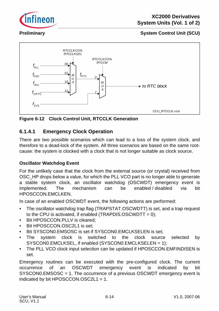
XC2000 DerivativesSystem Units (Vol. 1 of 2)
System Control Unit (SCU)Preliminary
Figure 6-12 Clock Control Unit, RTCCLK Generation
6.1.4.1 Emergency Clock OperationThere are two possible scenarios which can lead to a loss of the system clock, andtherefore to a dead-lock of the system. All three scenarios are based on the same root-cause: the system is clocked with a clock that is not longer suitable as clock source.
Oscillator Watchdog EventFor the unlikely case that the clock from the external source (or crystal) received fromOSC_HP drops below a value, for which the PLL VCO part is no longer able to generatea stable system clock, an oscillator watchdog (OSCWDT) emergency event isimplemented. The mechanism can be enabled / disabled via bitHPOSCCON.EMCLKEN.In case of an enabled OSCWDT event, the following actions are performed:• The oscillator watchdog trap flag (TRAPSTAT.OSCWDTT) is set, and a trap request
to the CPU is activated, if enabled (TRAPDIS.OSCWDTT = 0);• Bit HPOSCCON.PLLV is cleared;• Bit HPOSCCON.OSC2L1 is set;• Bit SYSCON0.EMSOSC is set if SYSCON0.EMCLKSELEN is set;• The system clock is switched to the clock source selected by
SYSCON0.EMCLKSEL, if enabled (SYSCON0.EMCLKSELEN = 1);• The PLL VCO clock input selection can be updated if HPOSCCON.EMFINDISEN is
set.Emergency routines can be executed with the pre-configured clock. The currentoccurrence of an OSCWDT emergency event is indicated by bitSYSCON0.EMSOSC = 1. The occurrence of a previous OSCWDT emergency event isindicated by bit HPOSCCON.OSC2L1 = 1.
CCU_RTCCLK.vsd
fWU
fOSC
fPLL
MUX
00
01
10
11
MUX
0
1
to RTC block
RTCCLKCON.RTCCLKSEL
fDRTC
fSYS
RTCCLKCON.RTCCM
fRTC
User’s Manual 6-14 V1.0, 2007-06SCU, V1.1
XC2000 DerivativesSystem Units (Vol. 1 of 2)
System Control Unit (SCU)Preliminary
An OSCWDT emergency event is terminated by setting bit STATCLR0.EMCOSC. BitHPOSCCON.OSC2L0 = 1 indicates that an OSCWDT emergency event condition is nolonger valid.Note: The oscillator watchdog does not refer to the start-up process. Bit
HPOSCCON.PLLV has to be set first before the oscillator watchdog trapgeneration mechanism is activated.
PLL VCO Loss of Lock EventFor the unlikely case that the PLL VCO part is no longer able to generate a stable systemclock, a PLL VCO loss of lock (VCOLCK) emergency event is implemented. Themechanism can be enabled / disabled via bit PLLCON1.EMCLKEN.In case of an enabled VCOLCK event, the following actions are performed:• The PLL VCO loss of lock trap flag (TRAPSTAT.VCOLCKT) is set, and a trap request
to the CPU is activated, if enabled (TRAPDIS.VCOLCKT = 0);• Bit PLLSTAT.VCOLOCK is cleared;• Bit PLLSTAT.VCOL0 is set;• Bit SYSCON0.EMSVCO is set if SYSCON0.EMCLKSELEN is set;• The system clock is switched to the clock source selected by
SYSCON0.EMCLKSEL, if enabled (SYSCON0.EMCLKSELEN = 1);• The PLL VCO clock input select can be updated if PLLCON1.EMFINDISEN is set.Emergency routines can be executed with the pre-configured clock. The currentoccurrence of a VCOLCK emergency event is indicated by bit SYSCON0.EMSVCO = 1.The occurrence of a previous VCOLCK emergency event is indicated by bitPLLSTAT.VCOL0 = 1.A VCOLCK emergency event is terminated by setting bit STATCLR0.EMCVCO. BitPLLSTAT.VCOL1 = 1 indicates that a VCOLCK emergency event condition is no longervalid.
6.1.5 External Clock OutputAn external clock output is provided via pin EXTCLK. This external clock can beenabled/disabled via bit EXTCON.EN. Each of the six clocks which defines a clockdomain can be individually be selected to be output at pin EXTCLK. This is configuredvia bit field EXTCON.SEL. Changing the content of bit field EXTCON.SEL can lead tospikes at pin EXTCLK.Additionally, a connection to the CAPCOM60 module is implemented, to support thestart-up control of an external crystal for the system clock generation. The first time,before the system clock is generated based on an external crystal, one should wait for1000 cycles of the crystal clock before the clock control system is changed to ExternalCrystal Mode. The 1000 cycles can be counted with CC60, using fOSC as count input forthe counter.
User’s Manual 6-15 V1.0, 2007-06SCU, V1.1
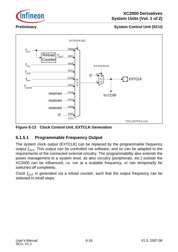
XC2000 DerivativesSystem Units (Vol. 1 of 2)
System Control Unit (SCU)Preliminary
Figure 6-13 Clock Control Unit, EXTCLK Generation
6.1.5.1 Programmable Frequency OutputThe system clock output (EXTCLK) can be replaced by the programmable frequencyoutput fOUT. This output can be controlled via software, and so can be adapted to therequirements of the connected external circuitry. The programmability also extends thepower management to a system level, as also circuitry (peripherals, etc.) outside theXC2000 can be influenced, i.e. run at a scalable frequency, or can temporarily beswitched off completely.Clock fOUT is generated via a reload counter, such that the output frequency can beselected in small steps.
CCU_EXTCLK.vsd
MUX
0000
EXTCON.SEL
EXTCON.EN
fOUT 0001
0010
0011
0100
0101
0110
0111
1000
1001...
1111'0'
to CC60
EXTCLK
ReloadCounter
fWU
fOSC
fPLL
fDIRIN
fSYS
MUX
'0' 0
1
reserved
reserved
reserved
User’s Manual 6-16 V1.0, 2007-06SCU, V1.1
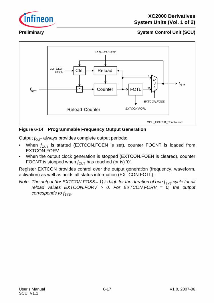
XC2000 DerivativesSystem Units (Vol. 1 of 2)
System Control Unit (SCU)Preliminary
Figure 6-14 Programmable Frequency Output Generation
Output fOUT always provides complete output periods:• When fOUT is started (EXTCON.FOEN is set), counter FOCNT is loaded from
EXTCON.FORV• When the output clock generation is stopped (EXTCON.FOEN is cleared), counter
FOCNT is stopped when fOUT has reached (or is) ’0’.Register EXTCON provides control over the output generation (frequency, waveform,activation) as well as holds all status information (EXTCON.FOTL).Note: The output (for EXTCON.FOSS= 1) is high for the duration of one fSYS cycle for all
reload values EXTCON.FORV > 0. For EXTCON.FORV = 0, the outputcorresponds to fSYS.
CCU_EXTCLK_Counter.vsd
0
EXTCON.FOTL
fOUT
CounterfSYS FOTL
MUX
Ctrl.EXTCON.FOEN Reload
EXTCON.FORV
EXTCON.FOSS
1
Reload Counter
User’s Manual 6-17 V1.0, 2007-06SCU, V1.1

XC2000 DerivativesSystem Units (Vol. 1 of 2)
System Control Unit (SCU)Preliminary
6.1.6 CGU Registers
6.1.6.1 Wake-up Clock RegisterThis register controls the setting of the Wake-Up clock, OSC_WU.
6.1.6.2 High Precision Oscillator RegisterThis register controls the setting of the High-Precision Oscillator, OSC_HP.
WUOSCCONWake-up OSC Control Register ESFR (F1AEH/D7H) Reset Value: 0000H
15 14 13 12 11 10 9 8 7 6 5 4 3 2 1 0
0 DIS PWSEL FREQSEL
r rw rw rw
Field Bits Type DescriptionFREQSEL [1:0] rw Clock Frequency Selection
The values for the different settings are listed in the data sheet.Note: This value should only be changed when the
wake-up clock is not used as source for thesystem clock.
PWSEL [3:2] rw Power Consumption SelectionThe values for the different settings are listed in the data sheet.Note: This value should only be changed when the
wake-up clock is not used as source for thesystem clock.
DIS 4 rw Clock Disable0B The clock is enabled1B The clock is disabled
0 [15:5] r ReservedRead as 0; should be written with 0.
User’s Manual 6-18 V1.0, 2007-06SCU, V1.1
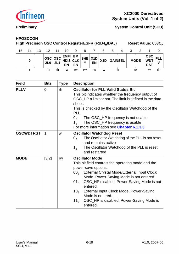
XC2000 DerivativesSystem Units (Vol. 1 of 2)
System Control Unit (SCU)Preliminary
HPOSCCONHigh Precision OSC Control RegisterESFR (F1B4H/DAH) Reset Value: 053CH
15 14 13 12 11 10 9 8 7 6 5 4 3 2 1 0
0 OSC2L0
OSC2L1
EMFINDISEN
EMCLKEN
SHBY
X1DEN X1D GAINSEL MODE
OSCWDTRST
PLLV
r rh rh rw rw rw rw rw rh rw w rh
Field Bits Type DescriptionPLLV 0 rh Oscillator for PLL Valid Status Bit
This bit indicates whether the frequency output of OSC_HP a limit or not. The limit is defined in the data sheet.This is checked by the Oscillator Watchdog of the PLL.0B The OSC_HP frequency is not usable1B The OSC_HP frequency is usableFor more information see Chapter 6.1.3.3.
OSCWDTRST 1 w Oscillator Watchdog Reset0B The Oscillator Watchdog of the PLL is not reset
and remains active1B The Oscillator Watchdog of the PLL is reset
and restartedMODE [3:2] rw Oscillator Mode
This bit field controls the operating mode and thepower-save options.00B External Crystal Mode/External Input Clock
Mode. Power-Saving Mode is not entered.01B OSC_HP disabled, Power-Saving Mode is not
entered. 10B External Input Clock Mode, Power-Saving
Mode is entered.11B OSC_HP is disabled, Power-Saving Mode is
entered.
User’s Manual 6-19 V1.0, 2007-06SCU, V1.1

XC2000 DerivativesSystem Units (Vol. 1 of 2)
System Control Unit (SCU)Preliminary
GAINSEL [5:4] rh Oscillator Gain Selection00B Gain configured for 4 to 8 MHz frequency
range01B Gain configured for 4 to 16 MHz frequency
range10B Gain configured for 4 to 20 MHz frequency
range11B Gain configured for 4 to 25 MHz frequency
rangeValues for the different settings are listed in the data sheet.
X1D 6 rh XTAL1 Data ValueThis bit monitors the inverted value (level) of pin XTAL1. If XTAL1 is not used as clock input, it can be used as general purpose input (GPI) pin.This bit is only updated if X1DEN is set.
X1DEN 7 rw XTAL1 Data Enable0B Bit X1D is not updated1B Bit X1D reflects inverted level of XTAL1
SHBY 8 rw Shaper BypassThe shaper modulates an input to fit to the requested shape. This is defined in the data sheet. If the input has already the correct shape the shaper can be bypassed.0B The shaper is not bypassed1B The shaper is bypassed
EMCLKEN 9 rw OSCWDT Emergency System Clock Source Select EnableThis bit defines whether the master clock multiplexer (MCM) should be controlled by bit field SYSCON0.EMCLKSEL in an OSCWDT emergency case.0B MCM controlled by SYSCON0.CLKSEL1B MCM controlled by SYSCON0.EMCLKSEL in
an OSCWDT emergency caseNote: Bit SYSCON0.EMCLKSELEN has to be set in
order to enable use of SYSCON0.EMCLKSEL
Field Bits Type Description
User’s Manual 6-20 V1.0, 2007-06SCU, V1.1

XC2000 DerivativesSystem Units (Vol. 1 of 2)
System Control Unit (SCU)Preliminary
6.1.6.3 PLL Clock RegisterThis register controls the settings of the internal PLL clock, OSC_PLL.
EMFINDISEN 10 rw Emergency Input Clock Disconnect EnableThis bit defines whether bit PLLSTAT.FINDIS is set in an emergency case.0B No update of PLLSTAT.FINDIS1B PLLSTAT.FINDIS is set in an OSCWDT
emergency caseOSC2L1 11 rh OSCWDT Reached Status
0B OSCWDT did not detect frequency below limit.1B OSCWDT detected an input frequency below
the limit.Note: Bit OSC2L1 can be cleared by setting bit
STATCLR1.OSC2L1CLR.OSC2L0 12 rh OSCWDT Left Status
0B OSCWDT did not detect frequency above limit.1B OSCWDT detected an input frequency above
the limit.Note: Bit OSC2L0 can be cleared by setting bit
STATCLR1.OSC2L0CLR.0 [15:13] r Reserved
Read as 0; should be written with 0.
PLLOSCCONPLL OSC Configuration RegisterESFR (F1B6H/DBH) Reset Value: 0000H
15 14 13 12 11 10 9 8 7 6 5 4 3 2 1 0
0 0 OSCPD
r rw rw
Field Bits Type DescriptionOSCPD 0 rw Internal Clock IOSC Power Saving Mode
0B IOSC is active1B IOSC is no longer powered
Field Bits Type Description
User’s Manual 6-21 V1.0, 2007-06SCU, V1.1
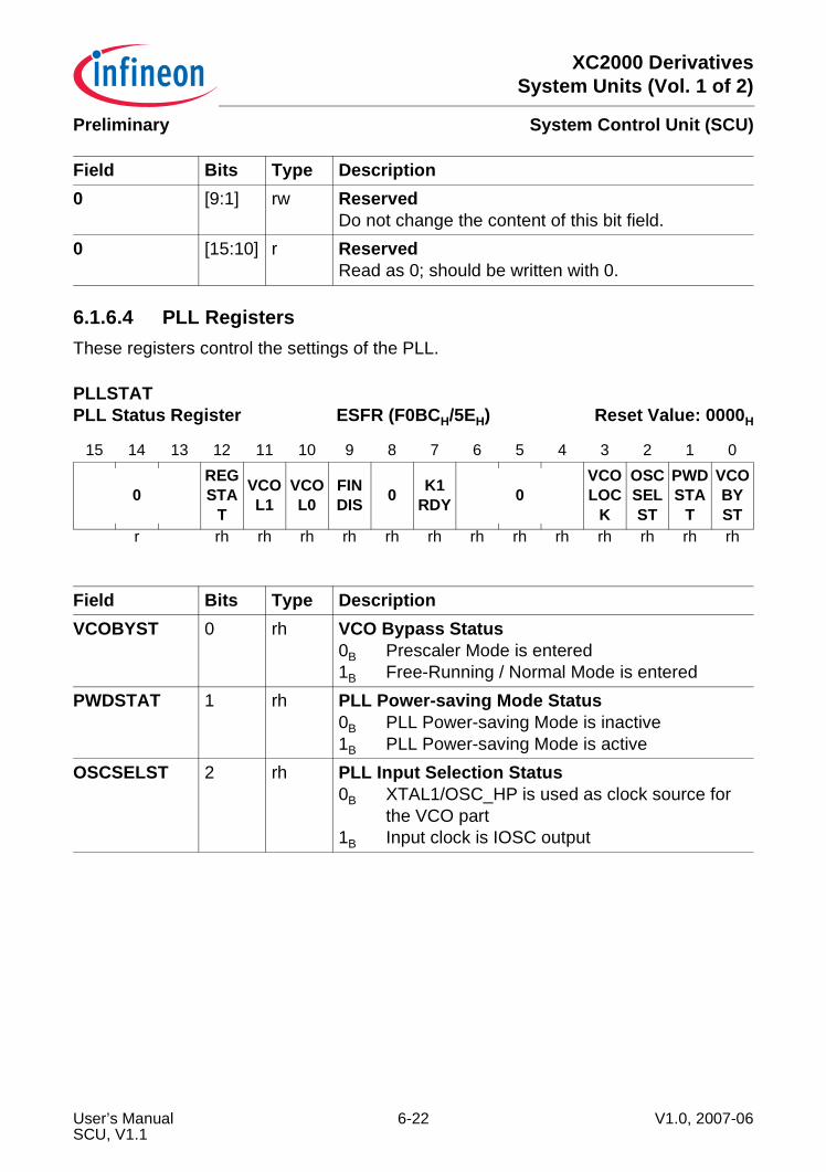
XC2000 DerivativesSystem Units (Vol. 1 of 2)
System Control Unit (SCU)Preliminary
6.1.6.4 PLL RegistersThese registers control the settings of the PLL.
0 [9:1] rw ReservedDo not change the content of this bit field.
0 [15:10] r ReservedRead as 0; should be written with 0.
PLLSTATPLL Status Register ESFR (F0BCH/5EH) Reset Value: 0000H
15 14 13 12 11 10 9 8 7 6 5 4 3 2 1 0
0REGSTA
T
VCOL1
VCOL0
FINDIS 0 K1
RDY 0VCOLOC
K
OSCSELST
PWDSTA
T
VCOBYST
r rh rh rh rh rh rh rh rh rh rh rh rh rh
Field Bits Type DescriptionVCOBYST 0 rh VCO Bypass Status
0B Prescaler Mode is entered1B Free-Running / Normal Mode is entered
PWDSTAT 1 rh PLL Power-saving Mode Status0B PLL Power-saving Mode is inactive1B PLL Power-saving Mode is active
OSCSELST 2 rh PLL Input Selection Status0B XTAL1/OSC_HP is used as clock source for
the VCO part1B Input clock is IOSC output
Field Bits Type Description
User’s Manual 6-22 V1.0, 2007-06SCU, V1.1
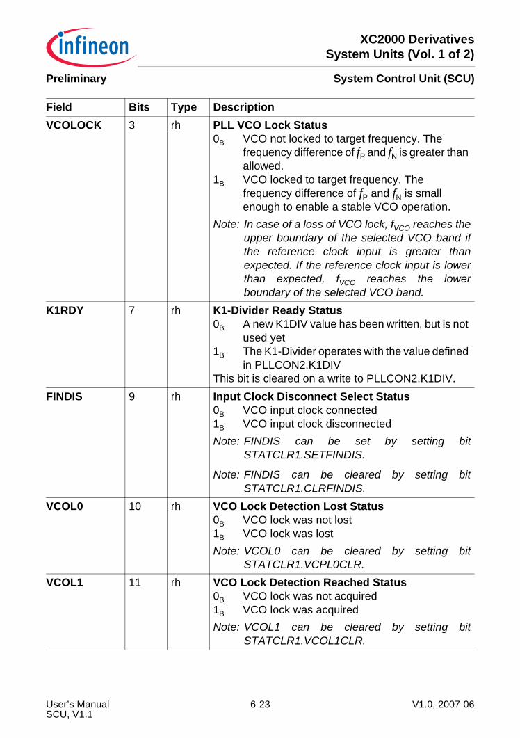
XC2000 DerivativesSystem Units (Vol. 1 of 2)
System Control Unit (SCU)Preliminary
VCOLOCK 3 rh PLL VCO Lock Status0B VCO not locked to target frequency. The
frequency difference of fP and fN is greater than allowed.
1B VCO locked to target frequency. The frequency difference of fP and fN is small enough to enable a stable VCO operation.
Note: In case of a loss of VCO lock, fVCO reaches theupper boundary of the selected VCO band ifthe reference clock input is greater thanexpected. If the reference clock input is lowerthan expected, fVCO reaches the lowerboundary of the selected VCO band.
K1RDY 7 rh K1-Divider Ready Status0B A new K1DIV value has been written, but is not
used yet1B The K1-Divider operates with the value defined
in PLLCON2.K1DIVThis bit is cleared on a write to PLLCON2.K1DIV.
FINDIS 9 rh Input Clock Disconnect Select Status0B VCO input clock connected1B VCO input clock disconnectedNote: FINDIS can be set by setting bit
STATCLR1.SETFINDIS.
Note: FINDIS can be cleared by setting bitSTATCLR1.CLRFINDIS.
VCOL0 10 rh VCO Lock Detection Lost Status0B VCO lock was not lost1B VCO lock was lostNote: VCOL0 can be cleared by setting bit
STATCLR1.VCPL0CLR.VCOL1 11 rh VCO Lock Detection Reached Status
0B VCO lock was not acquired1B VCO lock was acquiredNote: VCOL1 can be cleared by setting bit
STATCLR1.VCOL1CLR.
Field Bits Type Description
User’s Manual 6-23 V1.0, 2007-06SCU, V1.1
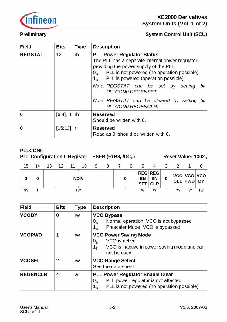
XC2000 DerivativesSystem Units (Vol. 1 of 2)
System Control Unit (SCU)Preliminary
REGSTAT 12 rh PLL Power Regulator StatusThe PLL has a separate internal power regulator, providing the power supply of the PLL.0B PLL is not powered (no operation possible)1B PLL is powered (operation possible)Note: REGSTAT can be set by setting bit
PLLCON0.REGENSET.
Note: REGSTAT can be cleared by setting bitPLLCON0.REGENCLR.
0 [6:4], 8 rh ReservedShould be written with 0.
0 [15:13] r ReservedRead as 0; should be written with 0.
PLLCON0PLL Configuration 0 Register ESFR (F1B8H/DCH) Reset Value: 1302H
15 14 13 12 11 10 9 8 7 6 5 4 3 2 1 0
0 0 NDIV 0REGENSET
REGEN
CLR0 VCO
SELVCOPWD
VCOBY
rw r rw r w w r rw rw rw
Field Bits Type DescriptionVCOBY 0 rw VCO Bypass
0B Normal operation, VCO is not bypassed1B Prescaler Mode; VCO is bypassed
VCOPWD 1 rw VCO Power Saving Mode0B VCO is active1B VCO is inactive in power saving mode and can
not be usedVCOSEL 2 rw VCO Range Select
See the data sheet. REGENCLR 4 w PLL Power Regulator Enable Clear
0B PLL power regulator is not affected1B PLL is not powered (no operation possible)
Field Bits Type Description
User’s Manual 6-24 V1.0, 2007-06SCU, V1.1
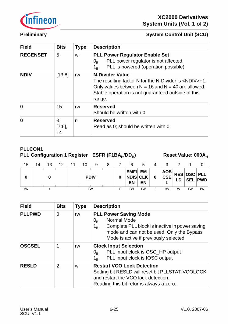
XC2000 DerivativesSystem Units (Vol. 1 of 2)
System Control Unit (SCU)Preliminary
REGENSET 5 w PLL Power Regulator Enable Set0B PLL power regulator is not affected1B PLL is powered (operation possible)
NDIV [13:8] rw N-Divider ValueThe resulting factor N for the N-Divider is <NDIV>+1.Only values between N = 16 and N = 40 are allowed. Stable operation is not guaranteed outside of thisrange.
0 15 rw ReservedShould be written with 0.
0 3,[7:6], 14
r ReservedRead as 0; should be written with 0.
PLLCON1PLL Configuration 1 Register ESFR (F1BAH/DDH) Reset Value: 000AH
15 14 13 12 11 10 9 8 7 6 5 4 3 2 1 0
0 0 PDIV 0EMFINDISEN
EMCLKEN
0AOSCSE
L
RESLD
OSCSEL
PLLPWD
rw r rw r rw rw r rw w rw rw
Field Bits Type DescriptionPLLPWD 0 rw PLL Power Saving Mode
0B Normal Mode1B Complete PLL block is inactive in power saving
mode and can not be used. Only the Bypass Mode is active if previously selected.
OSCSEL 1 rw Clock Input Selection0B PLL input clock is OSC_HP output1B PLL input clock is IOSC output
RESLD 2 w Restart VCO Lock DetectionSetting bit RESLD will reset bit PLLSTAT.VCOLOCKand restart the VCO lock detection. Reading this bit returns always a zero.
Field Bits Type Description
User’s Manual 6-25 V1.0, 2007-06SCU, V1.1
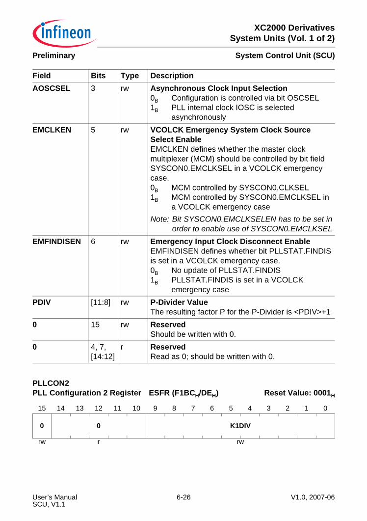
XC2000 DerivativesSystem Units (Vol. 1 of 2)
System Control Unit (SCU)Preliminary
AOSCSEL 3 rw Asynchronous Clock Input Selection0B Configuration is controlled via bit OSCSEL1B PLL internal clock IOSC is selected
asynchronouslyEMCLKEN 5 rw VCOLCK Emergency System Clock Source
Select EnableEMCLKEN defines whether the master clockmultiplexer (MCM) should be controlled by bit fieldSYSCON0.EMCLKSEL in a VCOLCK emergencycase.0B MCM controlled by SYSCON0.CLKSEL1B MCM controlled by SYSCON0.EMCLKSEL in
a VCOLCK emergency caseNote: Bit SYSCON0.EMCLKSELEN has to be set in
order to enable use of SYSCON0.EMCLKSELEMFINDISEN 6 rw Emergency Input Clock Disconnect Enable
EMFINDISEN defines whether bit PLLSTAT.FINDISis set in a VCOLCK emergency case.0B No update of PLLSTAT.FINDIS1B PLLSTAT.FINDIS is set in a VCOLCK
emergency casePDIV [11:8] rw P-Divider Value
The resulting factor P for the P-Divider is <PDIV>+10 15 rw Reserved
Should be written with 0.0 4, 7,
[14:12]r Reserved
Read as 0; should be written with 0.
PLLCON2PLL Configuration 2 Register ESFR (F1BCH/DEH) Reset Value: 0001H
15 14 13 12 11 10 9 8 7 6 5 4 3 2 1 0
0 0 K1DIV
rw r rw
Field Bits Type Description
User’s Manual 6-26 V1.0, 2007-06SCU, V1.1
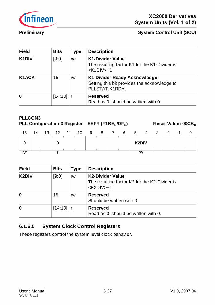
XC2000 DerivativesSystem Units (Vol. 1 of 2)
System Control Unit (SCU)Preliminary
6.1.6.5 System Clock Control RegistersThese registers control the system level clock behavior.
Field Bits Type DescriptionK1DIV [9:0] rw K1-Divider Value
The resulting factor K1 for the K1-Divider is<K1DIV>+1
K1ACK 15 rw K1-Divider Ready AcknowledgeSetting this bit provides the acknowledge to PLLSTAT.K1RDY.
0 [14:10] r ReservedRead as 0; should be written with 0.
PLLCON3PLL Configuration 3 Register ESFR (F1BEH/DFH) Reset Value: 00CBH
15 14 13 12 11 10 9 8 7 6 5 4 3 2 1 0
0 0 K2DIV
rw r rw
Field Bits Type DescriptionK2DIV [9:0] rw K2-Divider Value
The resulting factor K2 for the K2-Divider is<K2DIV>+1
0 15 rw ReservedShould be written with 0.
0 [14:10] r ReservedRead as 0; should be written with 0.
User’s Manual 6-27 V1.0, 2007-06SCU, V1.1
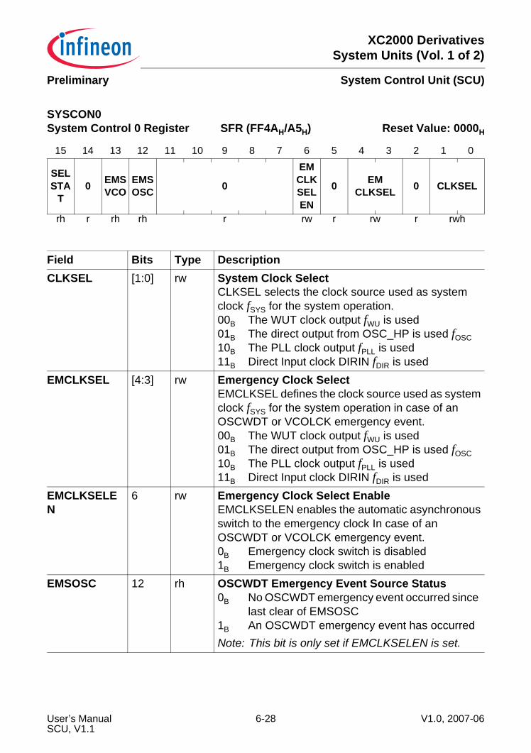
XC2000 DerivativesSystem Units (Vol. 1 of 2)
System Control Unit (SCU)Preliminary
SYSCON0System Control 0 Register SFR (FF4AH/A5H) Reset Value: 0000H
15 14 13 12 11 10 9 8 7 6 5 4 3 2 1 0
SELSTA
T0 EMS
VCOEMSOSC 0
EMCLKSELEN
0 EMCLKSEL 0 CLKSEL
rh r rh rh r rw r rw r rwh
Field Bits Type DescriptionCLKSEL [1:0] rw System Clock Select
CLKSEL selects the clock source used as systemclock fSYS for the system operation.00B The WUT clock output fWU is used01B The direct output from OSC_HP is used fOSC10B The PLL clock output fPLL is used11B Direct Input clock DIRIN fDIR is used
EMCLKSEL [4:3] rw Emergency Clock SelectEMCLKSEL defines the clock source used as systemclock fSYS for the system operation in case of anOSCWDT or VCOLCK emergency event.00B The WUT clock output fWU is used01B The direct output from OSC_HP is used fOSC10B The PLL clock output fPLL is used11B Direct Input clock DIRIN fDIR is used
EMCLKSELEN
6 rw Emergency Clock Select EnableEMCLKSELEN enables the automatic asynchronousswitch to the emergency clock In case of anOSCWDT or VCOLCK emergency event.0B Emergency clock switch is disabled1B Emergency clock switch is enabled
EMSOSC 12 rh OSCWDT Emergency Event Source Status0B No OSCWDT emergency event occurred since
last clear of EMSOSC1B An OSCWDT emergency event has occurredNote: This bit is only set if EMCLKSELEN is set.
User’s Manual 6-28 V1.0, 2007-06SCU, V1.1
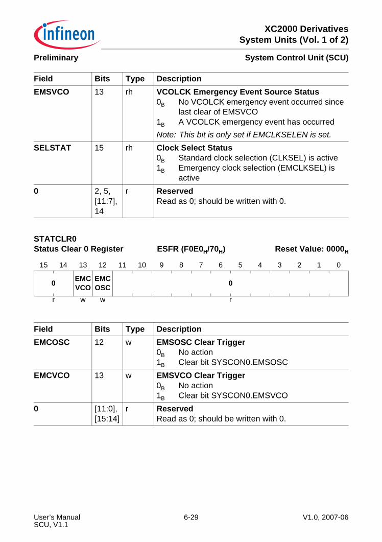
XC2000 DerivativesSystem Units (Vol. 1 of 2)
System Control Unit (SCU)Preliminary
EMSVCO 13 rh VCOLCK Emergency Event Source Status0B No VCOLCK emergency event occurred since
last clear of EMSVCO1B A VCOLCK emergency event has occurredNote: This bit is only set if EMCLKSELEN is set.
SELSTAT 15 rh Clock Select Status0B Standard clock selection (CLKSEL) is active1B Emergency clock selection (EMCLKSEL) is
active0 2, 5,
[11:7], 14
r ReservedRead as 0; should be written with 0.
STATCLR0Status Clear 0 Register ESFR (F0E0H/70H) Reset Value: 0000H
15 14 13 12 11 10 9 8 7 6 5 4 3 2 1 0
0 EMCVCO
EMCOSC 0
r w w r
Field Bits Type DescriptionEMCOSC 12 w EMSOSC Clear Trigger
0B No action1B Clear bit SYSCON0.EMSOSC
EMCVCO 13 w EMSVCO Clear Trigger0B No action1B Clear bit SYSCON0.EMSVCO
0 [11:0],[15:14]
r ReservedRead as 0; should be written with 0.
Field Bits Type Description
User’s Manual 6-29 V1.0, 2007-06SCU, V1.1
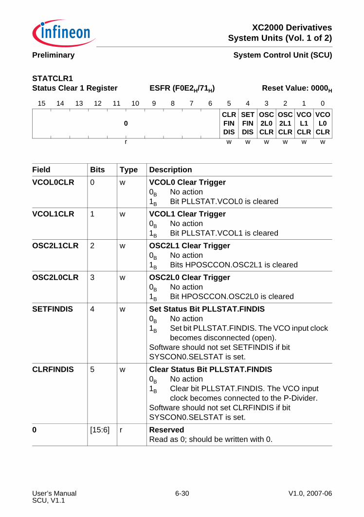
XC2000 DerivativesSystem Units (Vol. 1 of 2)
System Control Unit (SCU)Preliminary
STATCLR1Status Clear 1 Register ESFR (F0E2H/71H) Reset Value: 0000H
15 14 13 12 11 10 9 8 7 6 5 4 3 2 1 0
0CLRFINDIS
SETFINDIS
OSC2L0CLR
OSC2L1CLR
VCOL1
CLR
VCOL0
CLRr w w w w w w
Field Bits Type DescriptionVCOL0CLR 0 w VCOL0 Clear Trigger
0B No action1B Bit PLLSTAT.VCOL0 is cleared
VCOL1CLR 1 w VCOL1 Clear Trigger0B No action1B Bit PLLSTAT.VCOL1 is cleared
OSC2L1CLR 2 w OSC2L1 Clear Trigger0B No action1B Bits HPOSCCON.OSC2L1 is cleared
OSC2L0CLR 3 w OSC2L0 Clear Trigger0B No action1B Bit HPOSCCON.OSC2L0 is cleared
SETFINDIS 4 w Set Status Bit PLLSTAT.FINDIS0B No action1B Set bit PLLSTAT.FINDIS. The VCO input clock
becomes disconnected (open).Software should not set SETFINDIS if bit SYSCON0.SELSTAT is set.
CLRFINDIS 5 w Clear Status Bit PLLSTAT.FINDIS0B No action1B Clear bit PLLSTAT.FINDIS. The VCO input
clock becomes connected to the P-Divider.Software should not set CLRFINDIS if bit SYSCON0.SELSTAT is set.
0 [15:6] r ReservedRead as 0; should be written with 0.
User’s Manual 6-30 V1.0, 2007-06SCU, V1.1
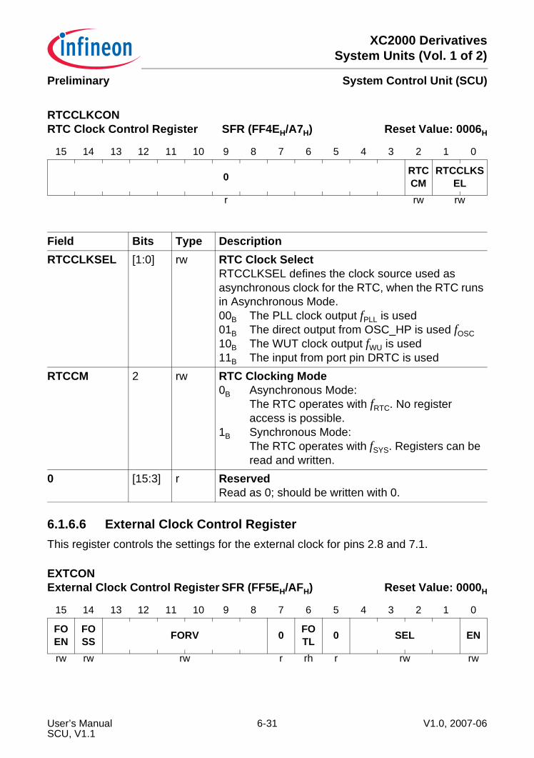
XC2000 DerivativesSystem Units (Vol. 1 of 2)
System Control Unit (SCU)Preliminary
6.1.6.6 External Clock Control RegisterThis register controls the settings for the external clock for pins 2.8 and 7.1.
RTCCLKCONRTC Clock Control Register SFR (FF4EH/A7H) Reset Value: 0006H
15 14 13 12 11 10 9 8 7 6 5 4 3 2 1 0
0 RTCCM
RTCCLKSEL
r rw rw
Field Bits Type DescriptionRTCCLKSEL [1:0] rw RTC Clock Select
RTCCLKSEL defines the clock source used asasynchronous clock for the RTC, when the RTC runsin Asynchronous Mode.00B The PLL clock output fPLL is used01B The direct output from OSC_HP is used fOSC10B The WUT clock output fWU is used11B The input from port pin DRTC is used
RTCCM 2 rw RTC Clocking Mode0B Asynchronous Mode:
The RTC operates with fRTC. No register access is possible.
1B Synchronous Mode:The RTC operates with fSYS. Registers can be read and written.
0 [15:3] r ReservedRead as 0; should be written with 0.
EXTCONExternal Clock Control Register SFR (FF5EH/AFH) Reset Value: 0000H
15 14 13 12 11 10 9 8 7 6 5 4 3 2 1 0
FOEN
FOSS FORV 0 FO
TL 0 SEL EN
rw rw rw r rh r rw rw
User’s Manual 6-31 V1.0, 2007-06SCU, V1.1
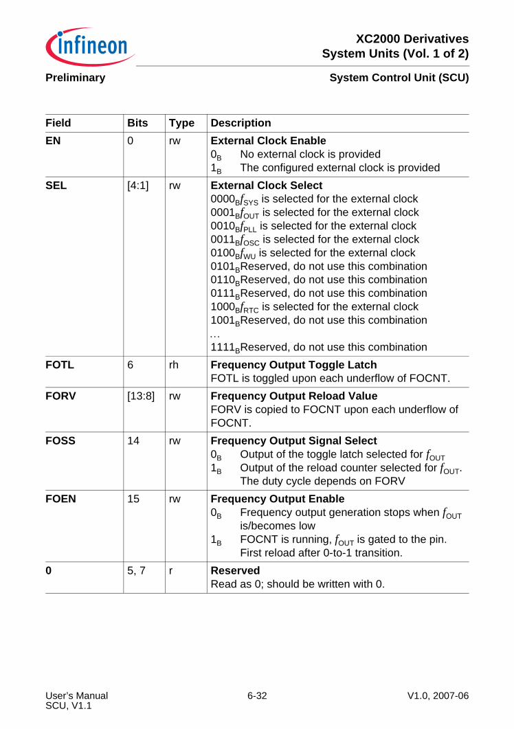
XC2000 DerivativesSystem Units (Vol. 1 of 2)
System Control Unit (SCU)Preliminary
Field Bits Type DescriptionEN 0 rw External Clock Enable
0B No external clock is provided1B The configured external clock is provided
SEL [4:1] rw External Clock Select0000BfSYS is selected for the external clock 0001BfOUT is selected for the external clock 0010BfPLL is selected for the external clock 0011BfOSC is selected for the external clock 0100BfWU is selected for the external clock 0101BReserved, do not use this combination0110BReserved, do not use this combination0111BReserved, do not use this combination1000BfRTC is selected for the external clock 1001BReserved, do not use this combination… 1111BReserved, do not use this combination
FOTL 6 rh Frequency Output Toggle LatchFOTL is toggled upon each underflow of FOCNT.
FORV [13:8] rw Frequency Output Reload ValueFORV is copied to FOCNT upon each underflow ofFOCNT.
FOSS 14 rw Frequency Output Signal Select0B Output of the toggle latch selected for fOUT1B Output of the reload counter selected for fOUT.
The duty cycle depends on FORVFOEN 15 rw Frequency Output Enable
0B Frequency output generation stops when fOUT is/becomes low
1B FOCNT is running, fOUT is gated to the pin.First reload after 0-to-1 transition.
0 5, 7 r ReservedRead as 0; should be written with 0.
User’s Manual 6-32 V1.0, 2007-06SCU, V1.1
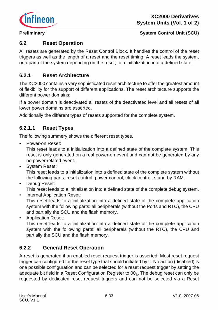
XC2000 DerivativesSystem Units (Vol. 1 of 2)
System Control Unit (SCU)Preliminary
6.2 Reset OperationAll resets are generated by the Reset Control Block. It handles the control of the resettriggers as well as the length of a reset and the reset timing. A reset leads the system,or a part of the system depending on the reset, to a initialization into a defined state.
6.2.1 Reset ArchitectureThe XC2000 contains a very sophisticated reset architecture to offer the greatest amountof flexibility for the support of different applications. The reset architecture supports thedifferent power domains:If a power domain is deactivated all resets of the deactivated level and all resets of alllower power domains are asserted.Additionally the different types of resets supported for the complete system.
6.2.1.1 Reset TypesThe following summery shows the different reset types.• Power-on Reset:
This reset leads to a initialization into a defined state of the complete system. Thisreset is only generated on a real power-on event and can not be generated by anyno power related event.
• System Reset:This reset leads to a initialization into a defined state of the complete system withoutthe following parts: reset control, power control, clock control, stand-by RAM.
• Debug Reset:This reset leads to a initialization into a defined state of the complete debug system.
• Internal Application Reset:This reset leads to a initialization into a defined state of the complete applicationsystem with the following parts: all peripherals (without the Ports and RTC), the CPUand partially the SCU and the flash memory.
• Application Reset:This reset leads to a initialization into a defined state of the complete applicationsystem with the following parts: all peripherals (without the RTC), the CPU andpartially the SCU and the flash memory.
6.2.2 General Reset OperationA reset is generated if an enabled reset request trigger is asserted. Most reset requesttrigger can configured for the reset type that should initiated by it. No action (disabled) isone possible configuration and can be selected for a reset request trigger by setting theadequate bit field in a Reset Configuration Register to 00B. The debug reset can only berequested by dedicated reset request triggers and can not be selected via a Reset
User’s Manual 6-33 V1.0, 2007-06SCU, V1.1

XC2000 DerivativesSystem Units (Vol. 1 of 2)
System Control Unit (SCU)Preliminary
Configuration Register. For more information see also registers RSTCON0 andRSTCON1.The duration of a reset is defined by two independent counters. One counter for thesystem and application reset types and one separate counter for the debug reset. Aseparate counter for the debug reset was implemented to allow a non-intrusiveadaptation of the reset length to the debugger needs without modification of theapplication setting.
6.2.2.1 Reset Counters (RSTCNTA and RSTCNTD)RSTCNTA is the reset counter that controls the reset length for all application relevantresets (system reset, internal application reset, and application reset). RSTCNTD is thereset counter that controls the reset length for the debug reset.The reset counters can be used for the following purposes:• First to control the length of the internal resets.• Second to configure the reset length in a way that the reset outputs via the ESRx pins
match with the reset input requirements of external blocks connected with the resetoutputs.
A reset counter RSTCNT is an 8-bit counter counting down from the reload value definedby RSTCNTCON.RELx (x = A or D). The counter is started by the reset control block assoon as a reset request trigger condition becomes active (for more information seeTable 6-4 and Table 6-5). Whether the counter has to be started or not depends on thereset request trigger and whether the counter is already active or not. In case of that thecounter is inactive, not counting down, it is always started. While the counter is alreadyactive it depends on the reset typ of the new reset request trigger that was asserted anewif the counter is restarted or not. This behavior is summarized in Table 6-4 andTable 6-5.
Table 6-4 Restart of RSTCNTAReset Active New Reset
Power-On System Reset
Debug Reset
Internal Application
Reset
Application Reset
System Reset
Restart No Restart No Restart No Restart No Restart
Internal Application Reset
Restart Restart No Restart No Restart No Restart
Application Reset
Restart Restart No Restart Restart No Restart
User’s Manual 6-34 V1.0, 2007-06SCU, V1.1
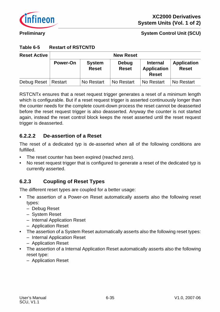
XC2000 DerivativesSystem Units (Vol. 1 of 2)
System Control Unit (SCU)Preliminary
RSTCNTx ensures that a reset request trigger generates a reset of a minimum lengthwhich is configurable. But if a reset request trigger is asserted continuously longer thanthe counter needs for the complete count-down process the reset cannot be deassertedbefore the reset request trigger is also deasserted. Anyway the counter is not startedagain, instead the reset control block keeps the reset asserted until the reset requesttrigger is deasserted.
6.2.2.2 De-assertion of a ResetThe reset of a dedicated typ is de-asserted when all of the following conditions arefulfilled.• The reset counter has been expired (reached zero).• No reset request trigger that is configured to generate a reset of the dedicated typ is
currently asserted.
6.2.3 Coupling of Reset TypesThe different reset types are coupled for a better usage:• The assertion of a Power-on Reset automatically asserts also the following reset
types:– Debug Reset– System Reset– Internal Application Reset– Application Reset
• The assertion of a System Reset automatically asserts also the following reset types:– Internal Application Reset– Application Reset
• The assertion of a Internal Application Reset automatically asserts also the followingreset type:– Application Reset
Table 6-5 Restart of RSTCNTDReset Active New Reset
Power-On System Reset
Debug Reset
Internal Application
Reset
Application Reset
Debug Reset Restart No Restart No Restart No Restart No Restart
User’s Manual 6-35 V1.0, 2007-06SCU, V1.1
XC2000 DerivativesSystem Units (Vol. 1 of 2)
System Control Unit (SCU)Preliminary
6.2.4 Debug Reset AssertionUnlike the other reset types a Debug Reset can only be asserted if the following twoconditions are valid:• A reset request trigger is asserted that request a debug reset• An Application Reset is active in the system
6.2.5 Example1:Reset request trigger A is asserted and leads to an Application Reset. If the reset requesttrigger is de-asserted before RSTCNTA reached zero the Application Reset is de-asserted when RSTCNTA reaches zero. If the reset request trigger is de-asserted afterRSTCNTA reached zero the Application Reset is de-asserted when the reset requesttrigger is de-asserted.
6.2.6 Example2:Reset request trigger A is asserted and leads to an Application Reset. Reset requesttrigger A is de-asserted before RSTCNTA reached zero. Reset request trigger B isasserted after reset request trigger A but before RSTCNTA reaches zero. Reset requesttrigger B is also configured to result in a Application Reset. If the reset request trigger Bis de-asserted before RSTCNTA reached zero the Application Reset is de-assertedwhen RSTCNTA reaches zero. If the reset request trigger B is de-asserted afterRSTCNTA reached zero the Application Reset is de-asserted when the reset requesttrigger B is de-asserted.
6.2.7 Example3:Reset request trigger A is asserted and leads to a System Reset. Reset request triggerA is de-asserted before RSTCNTA reached zero. Reset request trigger B is assertedafter reset request trigger A but before RSTCNTA reaches zero. Reset request trigger Bis configured to result in a Internal Application Reset. If the reset request trigger B is de-asserted before RSTCNTA reached zero the System, Internal Application, andApplication Resets are de-asserted when RSTCNTA reaches zero. If the reset requesttrigger B is de-asserted after RSTCNTA reached zero the Internal Application andApplication Resets are de-asserted when the reset request trigger B is de-asserted.
6.2.8 Reset Request Trigger SourcesThe following overview summarizes the different reset request trigger sources within thesystem.
User’s Manual 6-36 V1.0, 2007-06SCU, V1.1
XC2000 DerivativesSystem Units (Vol. 1 of 2)
System Control Unit (SCU)Preliminary
Power-On Reset Pin PORSTThe PORST input pin requests asynchronously a Power-on Reset by driving the PORSTpin low.
Supply Watchdog (SWD)If the power supply for I/O domain doesn’t reach the value required for properfunctionality, a non-synchronized reset request trigger is generated if the SWD resetgeneration is enabled. This ensures a reproducible behavior in the case of power-fail.This can also be used to restart the system without the usage of the PORST pin. As longas the I/O power domain does not get the required voltage level the system is held in thereset.
Core Power Validation (PVC_M and PVC_1)If the core power supply doesn’t reach the value required for proper functionality of mainpower domain (PVC_M), a reset request trigger can be forwarded to the system. Thegeneration of a Power-on Reset is configured by bit PVCMCON0.L1RSTEN = 1B. If thebit PVCMCON0.L1RSTEN = 1B a request trigger is asserted for PVC_M1 upon a levelcheck match. If the bit PVCMCON0.L2RSTEN = 1B a request trigger is asserted forPVC_M2 upon a level check match.If the core power supply doesn’t reach the value required for proper functionality ofapplication power domain (PVC_1), a reset request trigger can be forwarded to thesystem. The generation of a Power-on Reset for (Application Power Domain only) isconfigured by bit PVC1CON0.L1RSTEN = 1B. If the bit PVC1CON0.L1RSTEN = 1B arequest trigger is asserted for PVC_11 upon a level check match. If the bitPVC1CON0.L2RSTEN = 1B a request trigger is asserted for PVC_12 upon a level checkmatch.For more information about the Power Validation Circuit see Chapter 6.5.2.
ESR0/ESR1/ESR2 An ESR0/ESR1/ESR2 reset request trigger leads to a configurable reset. The type ofreset can be configured via RSTCON1.ESRx.The pins ESR0/ESR1/ESR2 can serve as an external reset input as well as a resetoutput (open drain) for Internal Application and Application Resets. For the ESR1 andESR2 additionally several GPIO pad triggers that can be enabled additionally via registerESREXCONx (x = 1 or 2) interfere with the ESR pin function. GPIO and ESR pin triggerscan be enabled/disabled individually and are combined for the reset trigger generation.Note: The reset output is only asserted for the duration the reset counter RSTCNTA is
active. During a possible reset extension the reset output is not longer asserted.
User’s Manual 6-37 V1.0, 2007-06SCU, V1.1
XC2000 DerivativesSystem Units (Vol. 1 of 2)
System Control Unit (SCU)Preliminary
If the pin ESR0/ESR1/ESR2 is enabled as reset output and the input level is low whilethe output stage is disabled (indicating that it is still driven low externally), the resetcircuitry holds the chip in reset until a high level is detected on ESR0/ESR1/ESR2. Theinternal output stage drives a low level during reset only while RSTCNTA is active. Itdeactivates the output stage when the time defined by RSTCNTCON.RELA has passed.
SoftwareA software reset request trigger leads to a configurable reset. The type of reset can beconfigured via RSTCON0.SW.
Watchdog TimerA WDT reset request trigger leads to a configurable reset. The type of reset can beconfigured via RSTCON1.WDT. A WDT reset is requested on a WDT overflow event.For more information see Chapter 6.8.
CPU A CPU reset request trigger leads to a configurable reset. The type of reset can beconfigured via RSTCON0.CPU. A CPU reset is requested when instruction SRST isexecuted.
Memory ParityA MP reset request trigger leads to a configurable reset. The type of reset can beconfigured via RSTCON1.MP. For more information see Section 3.12.
OCDS BlockThe OCDS block has several options to request different reset types:1. A Debug Reset either via the OCDS reset function or via bit CBS_OJCONF.RSTCL1
AND CBS_OJCONF.RSTCL32. A System Reset via bit CBS_OJCONF.RSTCL03. An Internal Application Reset via bit CBS_OJCONF.RSTCL24. An Application Reset via bit CBS_OJCONF.RSTCL3
User’s Manual 6-38 V1.0, 2007-06SCU, V1.1
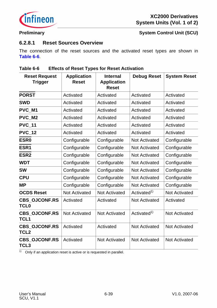
XC2000 DerivativesSystem Units (Vol. 1 of 2)
System Control Unit (SCU)Preliminary
6.2.8.1 Reset Sources OverviewThe connection of the reset sources and the activated reset types are shown inTable 6-6.
Table 6-6 Effects of Reset Types for Reset ActivationReset Request
TriggerApplication
ResetInternal
Application Reset
Debug Reset System Reset
PORST Activated Activated Activated ActivatedSWD Activated Activated Activated ActivatedPVC_M1 Activated Activated Activated ActivatedPVC_M2 Activated Activated Activated ActivatedPVC_11 Activated Activated Activated ActivatedPVC_12 Activated Activated Activated ActivatedESR0 Configurable Configurable Not Activated ConfigurableESR1 Configurable Configurable Not Activated ConfigurableESR2 Configurable Configurable Not Activated ConfigurableWDT Configurable Configurable Not Activated ConfigurableSW Configurable Configurable Not Activated ConfigurableCPU Configurable Configurable Not Activated ConfigurableMP Configurable Configurable Not Activated ConfigurableOCDS Reset Not Activated Not Activated Activated1)
1) Only if an application reset is active or is requested in parallel.
Not ActivatedCBS_OJCONF.RSTCL0
Activated Activated Not Activated Activated
CBS_OJCONF.RSTCL1
Not Activated Not Activated Activated1) Not Activated
CBS_OJCONF.RSTCL2
Activated Activated Not Activated Not Activated
CBS_OJCONF.RSTCL3
Activated Not Activated Not Activated Not Activated
User’s Manual 6-39 V1.0, 2007-06SCU, V1.1
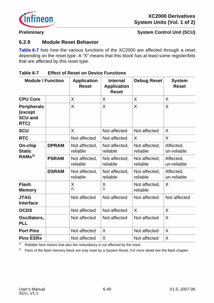
XC2000 DerivativesSystem Units (Vol. 1 of 2)
System Control Unit (SCU)Preliminary
6.2.9 Module Reset BehaviorTable 6-7 lists how the various functions of the XC2000 are affected through a resetdepending on the reset type. A “X” means that this block has at least some register/bitsthat are affected by this reset type.
Table 6-7 Effect of Reset on Device Functions Module / Function Application
ResetInternal
Application Reset
Debug Reset System Reset
CPU Core X X X XPeripherals(except SCU and RTC)
X X X X
SCU X Not affected Not affected XRTC Not affected Not affected X XOn-chip Static RAMs1)
1) Reliable here means that also the redundancy is not affected by the reset.
DPRAM Not affected,reliable
Not affected,reliable
Not affected,reliable
Affected,un-reliable
PSRAM Not affected,reliable
Not affected,reliable
Not affected,reliable
Affected,un-reliable
DSRAM Not affected,reliable
Not affected,reliable
Not affected,reliable
Affected,un-reliable
Flash Memory
X2)
2) Parts of the flash memory block are only reset by a System Reset. For more detail see the flash chapter.
X2)
Not affected,reliable
X
JTAG Interface
Not affected Not affected Not affected Not affected
OCDS Not affected Not affected X XOscillators, PLL
Not affected Not affected Not affected X
Port Pins Not affected X Not affected XPins ESRx Not affected X Not affected X
User’s Manual 6-40 V1.0, 2007-06SCU, V1.1
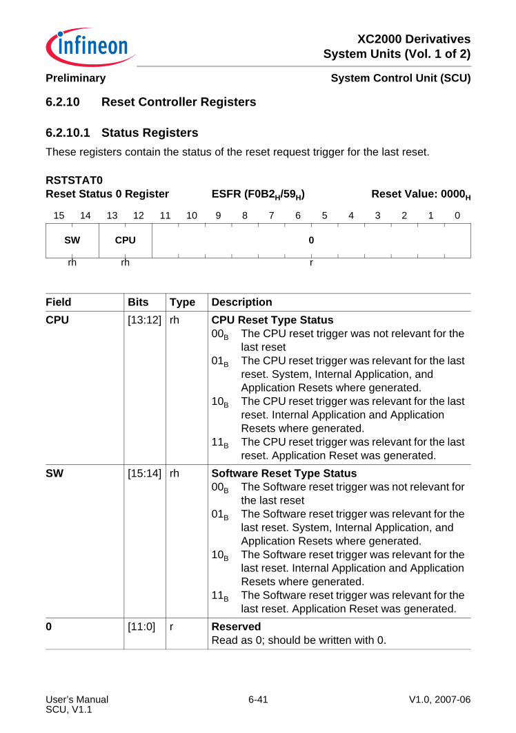
XC2000 DerivativesSystem Units (Vol. 1 of 2)
System Control Unit (SCU)Preliminary
6.2.10 Reset Controller Registers
6.2.10.1 Status RegistersThese registers contain the status of the reset request trigger for the last reset.
RSTSTAT0Reset Status 0 Register ESFR (F0B2H/59H) Reset Value: 0000H
15 14 13 12 11 10 9 8 7 6 5 4 3 2 1 0
SW CPU 0
rh rh r
Field Bits Type DescriptionCPU [13:12] rh CPU Reset Type Status
00B The CPU reset trigger was not relevant for the last reset
01B The CPU reset trigger was relevant for the last reset. System, Internal Application, and Application Resets where generated.
10B The CPU reset trigger was relevant for the last reset. Internal Application and Application Resets where generated.
11B The CPU reset trigger was relevant for the last reset. Application Reset was generated.
SW [15:14] rh Software Reset Type Status00B The Software reset trigger was not relevant for
the last reset01B The Software reset trigger was relevant for the
last reset. System, Internal Application, and Application Resets where generated.
10B The Software reset trigger was relevant for the last reset. Internal Application and Application Resets where generated.
11B The Software reset trigger was relevant for the last reset. Application Reset was generated.
0 [11:0] r ReservedRead as 0; should be written with 0.
User’s Manual 6-41 V1.0, 2007-06SCU, V1.1
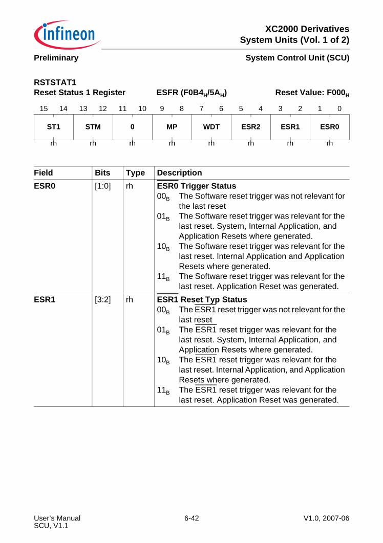
XC2000 DerivativesSystem Units (Vol. 1 of 2)
System Control Unit (SCU)Preliminary
RSTSTAT1Reset Status 1 Register ESFR (F0B4H/5AH) Reset Value: F000H
15 14 13 12 11 10 9 8 7 6 5 4 3 2 1 0
ST1 STM 0 MP WDT ESR2 ESR1 ESR0
rh rh rh rh rh rh rh rh
Field Bits Type DescriptionESR0 [1:0] rh ESR0 Trigger Status
00B The Software reset trigger was not relevant for the last reset
01B The Software reset trigger was relevant for the last reset. System, Internal Application, and Application Resets where generated.
10B The Software reset trigger was relevant for the last reset. Internal Application and Application Resets where generated.
11B The Software reset trigger was relevant for the last reset. Application Reset was generated.
ESR1 [3:2] rh ESR1 Reset Typ Status00B The ESR1 reset trigger was not relevant for the
last reset01B The ESR1 reset trigger was relevant for the
last reset. System, Internal Application, and Application Resets where generated.
10B The ESR1 reset trigger was relevant for the last reset. Internal Application, and Application Resets where generated.
11B The ESR1 reset trigger was relevant for the last reset. Application Reset was generated.
User’s Manual 6-42 V1.0, 2007-06SCU, V1.1
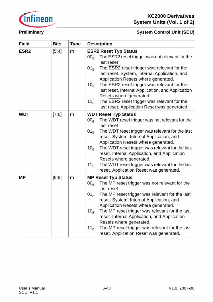
XC2000 DerivativesSystem Units (Vol. 1 of 2)
System Control Unit (SCU)Preliminary
ESR2 [5:4] rh ESR2 Reset Typ Status00B The ESR2 reset trigger was not relevant for the
last reset01B The ESR2 reset trigger was relevant for the
last reset. System, Internal Application, and Application Resets where generated.
10B The ESR2 reset trigger was relevant for the last reset. Internal Application, and Application Resets where generated.
11B The ESR2 reset trigger was relevant for the last reset. Application Reset was generated.
WDT [7:6] rh WDT Reset Typ Status00B The WDT reset trigger was not relevant for the
last reset01B The WDT reset trigger was relevant for the last
reset. System, Internal Application, and Application Resets where generated.
10B The WDT reset trigger was relevant for the last reset. Internal Application, and Application Resets where generated.
11B The WDT reset trigger was relevant for the last reset. Application Reset was generated.
MP [9:8] rh MP Reset Typ Status00B The MP reset trigger was not relevant for the
last reset01B The MP reset trigger was relevant for the last
reset. System, Internal Application, and Application Resets where generated.
10B The MP reset trigger was relevant for the last reset. Internal Application, and Application Resets where generated.
11B The MP reset trigger was relevant for the last reset. Application Reset was generated.
Field Bits Type Description
User’s Manual 6-43 V1.0, 2007-06SCU, V1.1
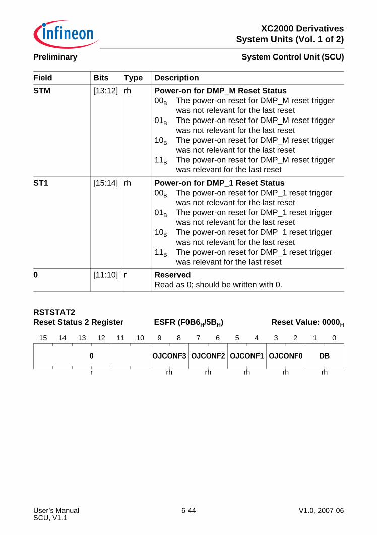
XC2000 DerivativesSystem Units (Vol. 1 of 2)
System Control Unit (SCU)Preliminary
STM [13:12] rh Power-on for DMP_M Reset Status00B The power-on reset for DMP_M reset trigger
was not relevant for the last reset01B The power-on reset for DMP_M reset trigger
was not relevant for the last reset10B The power-on reset for DMP_M reset trigger
was not relevant for the last reset11B The power-on reset for DMP_M reset trigger
was relevant for the last resetST1 [15:14] rh Power-on for DMP_1 Reset Status
00B The power-on reset for DMP_1 reset trigger was not relevant for the last reset
01B The power-on reset for DMP_1 reset trigger was not relevant for the last reset
10B The power-on reset for DMP_1 reset trigger was not relevant for the last reset
11B The power-on reset for DMP_1 reset trigger was relevant for the last reset
0 [11:10] r ReservedRead as 0; should be written with 0.
RSTSTAT2 Reset Status 2 Register ESFR (F0B6H/5BH) Reset Value: 0000H
15 14 13 12 11 10 9 8 7 6 5 4 3 2 1 0
0 OJCONF3 OJCONF2 OJCONF1 OJCONF0 DB
r rh rh rh rh rh
Field Bits Type Description
User’s Manual 6-44 V1.0, 2007-06SCU, V1.1
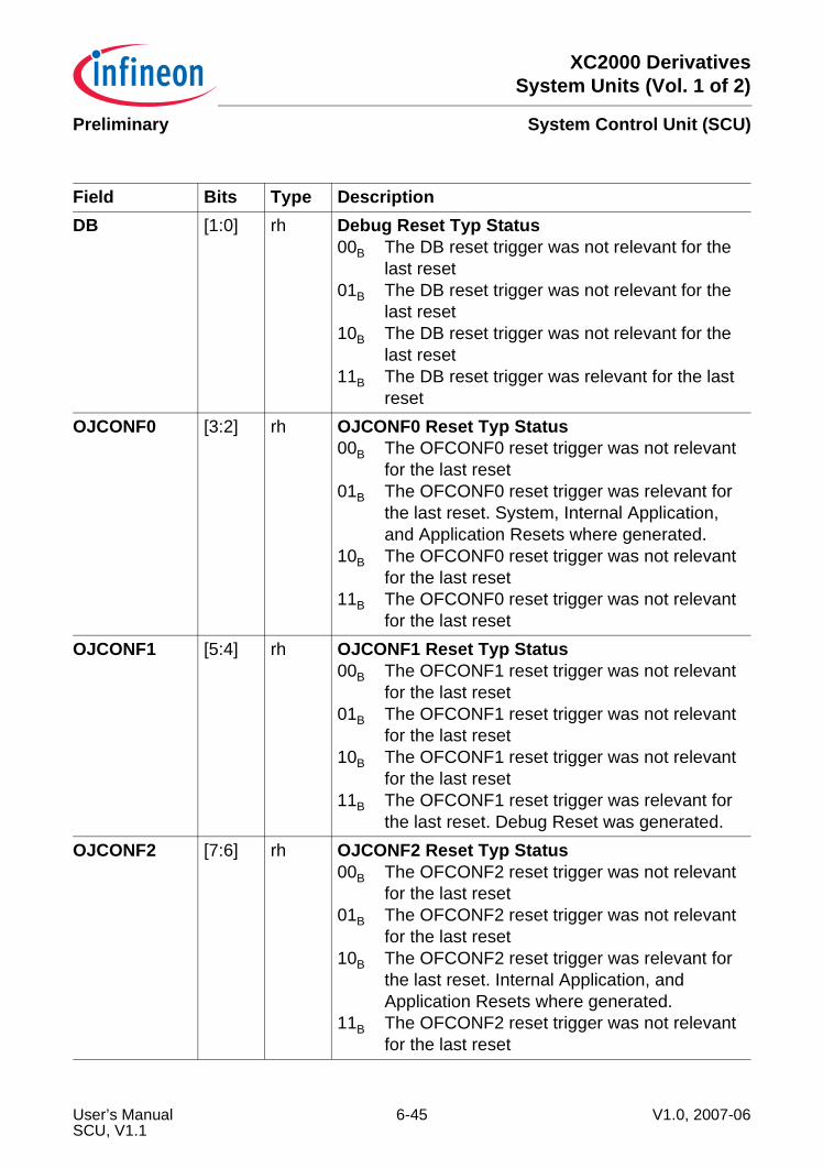
XC2000 DerivativesSystem Units (Vol. 1 of 2)
System Control Unit (SCU)Preliminary
Field Bits Type DescriptionDB [1:0] rh Debug Reset Typ Status
00B The DB reset trigger was not relevant for the last reset
01B The DB reset trigger was not relevant for the last reset
10B The DB reset trigger was not relevant for the last reset
11B The DB reset trigger was relevant for the last reset
OJCONF0 [3:2] rh OJCONF0 Reset Typ Status00B The OFCONF0 reset trigger was not relevant
for the last reset01B The OFCONF0 reset trigger was relevant for
the last reset. System, Internal Application, and Application Resets where generated.
10B The OFCONF0 reset trigger was not relevant for the last reset
11B The OFCONF0 reset trigger was not relevant for the last reset
OJCONF1 [5:4] rh OJCONF1 Reset Typ Status00B The OFCONF1 reset trigger was not relevant
for the last reset01B The OFCONF1 reset trigger was not relevant
for the last reset10B The OFCONF1 reset trigger was not relevant
for the last reset11B The OFCONF1 reset trigger was relevant for
the last reset. Debug Reset was generated.OJCONF2 [7:6] rh OJCONF2 Reset Typ Status
00B The OFCONF2 reset trigger was not relevant for the last reset
01B The OFCONF2 reset trigger was not relevant for the last reset
10B The OFCONF2 reset trigger was relevant for the last reset. Internal Application, and Application Resets where generated.
11B The OFCONF2 reset trigger was not relevant for the last reset
User’s Manual 6-45 V1.0, 2007-06SCU, V1.1
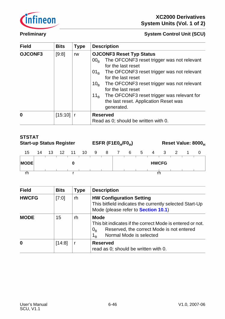
XC2000 DerivativesSystem Units (Vol. 1 of 2)
System Control Unit (SCU)Preliminary
OJCONF3 [9:8] rw OJCONF3 Reset Typ Status00B The OFCONF3 reset trigger was not relevant
for the last reset01B The OFCONF3 reset trigger was not relevant
for the last reset10B The OFCONF3 reset trigger was not relevant
for the last reset11B The OFCONF3 reset trigger was relevant for
the last reset. Application Reset was generated.
0 [15:10] r ReservedRead as 0; should be written with 0.
STSTAT Start-up Status Register ESFR (F1E0H/F0H) Reset Value: 8000H
15 14 13 12 11 10 9 8 7 6 5 4 3 2 1 0
MODE 0 HWCFG
rh r rh
Field Bits Type DescriptionHWCFG [7:0] rh HW Configuration Setting
This bitfield indicates the currently selected Start-Up Mode (please refer to Section 10.1)
MODE 15 rh ModeThis bit indicates if the correct Mode is entered or not.0B Reserved, the correct Mode is not entered1B Normal Mode is selected
0 [14:8] r Reservedread as 0; should be written with 0.
Field Bits Type Description
User’s Manual 6-46 V1.0, 2007-06SCU, V1.1
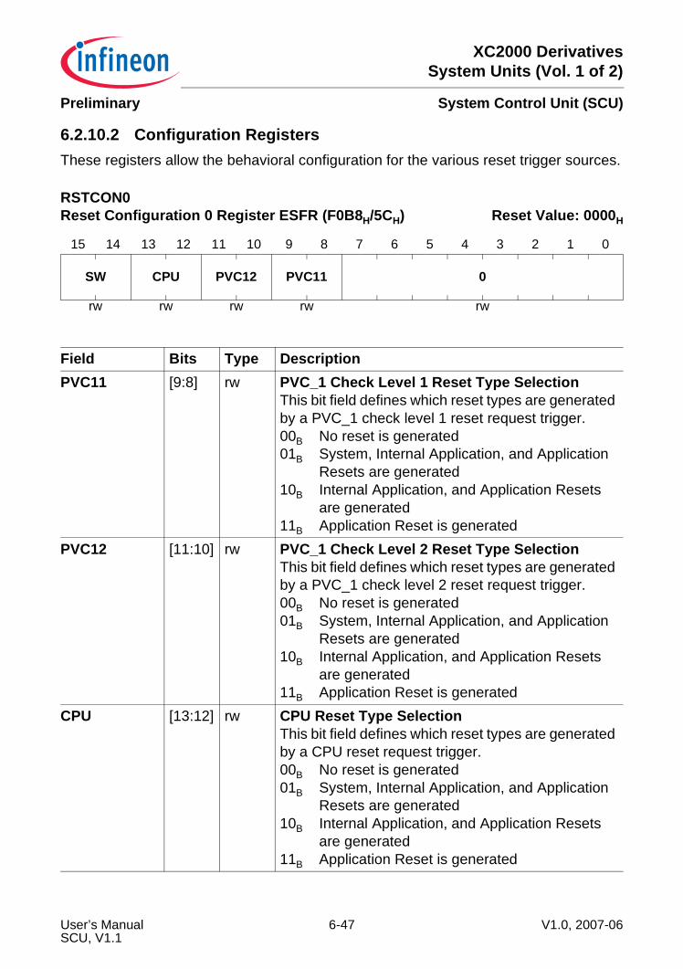
XC2000 DerivativesSystem Units (Vol. 1 of 2)
System Control Unit (SCU)Preliminary
6.2.10.2 Configuration RegistersThese registers allow the behavioral configuration for the various reset trigger sources.
RSTCON0Reset Configuration 0 Register ESFR (F0B8H/5CH) Reset Value: 0000H
15 14 13 12 11 10 9 8 7 6 5 4 3 2 1 0
SW CPU PVC12 PVC11 0
rw rw rw rw rw
Field Bits Type DescriptionPVC11 [9:8] rw PVC_1 Check Level 1 Reset Type Selection
This bit field defines which reset types are generated by a PVC_1 check level 1 reset request trigger.00B No reset is generated01B System, Internal Application, and Application
Resets are generated10B Internal Application, and Application Resets
are generated11B Application Reset is generated
PVC12 [11:10] rw PVC_1 Check Level 2 Reset Type SelectionThis bit field defines which reset types are generated by a PVC_1 check level 2 reset request trigger.00B No reset is generated01B System, Internal Application, and Application
Resets are generated10B Internal Application, and Application Resets
are generated11B Application Reset is generated
CPU [13:12] rw CPU Reset Type SelectionThis bit field defines which reset types are generated by a CPU reset request trigger.00B No reset is generated01B System, Internal Application, and Application
Resets are generated10B Internal Application, and Application Resets
are generated11B Application Reset is generated
User’s Manual 6-47 V1.0, 2007-06SCU, V1.1

XC2000 DerivativesSystem Units (Vol. 1 of 2)
System Control Unit (SCU)Preliminary
SW [15:14] rw Software Reset Type SelectionThis bit field defines which reset types are generated by a software reset request trigger.00B No reset is generated01B System, Internal Application, and Application
Resets are generated10B Internal Application, and Application Resets
are generated11B Application Reset is generated
0 [0:7] rw ReservedShould be written with 0.
RSTCON1Reset Configuration 1 Register ESFR (F0BAH/5DH) Reset Value: 0002H
15 14 13 12 11 10 9 8 7 6 5 4 3 2 1 0
0 MP WDT ESR2 ESR1 ESR0
rw rw rw rw rw rw
Field Bits Type DescriptionESR0 [1:0] rw ESR0 Reset Type Selection
This bit field defines which reset types are generated by a ESR0 reset request trigger.00B No reset is generated01B System, Internal Application, and Application
Resets are generated10B Internal Application, and Application Resets
are generated11B Application Reset is generated
Field Bits Type Description
User’s Manual 6-48 V1.0, 2007-06SCU, V1.1
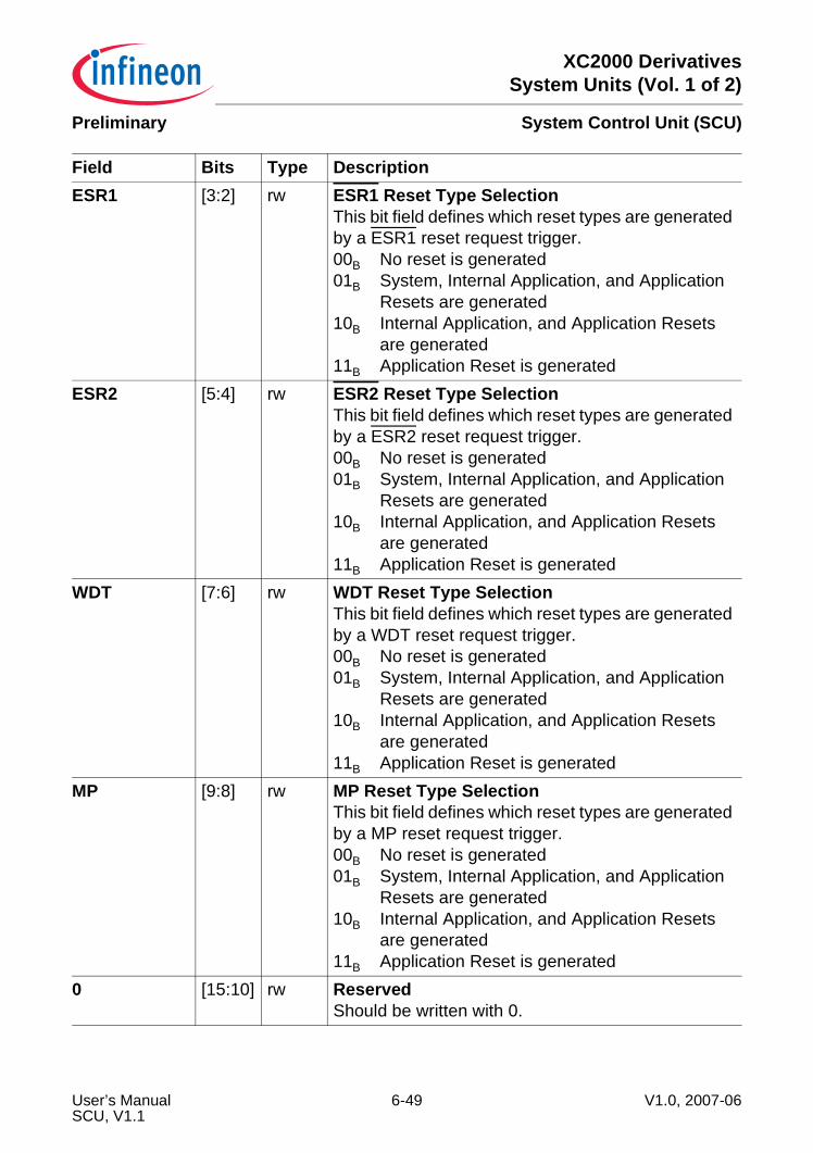
XC2000 DerivativesSystem Units (Vol. 1 of 2)
System Control Unit (SCU)Preliminary
ESR1 [3:2] rw ESR1 Reset Type SelectionThis bit field defines which reset types are generated by a ESR1 reset request trigger.00B No reset is generated01B System, Internal Application, and Application
Resets are generated10B Internal Application, and Application Resets
are generated11B Application Reset is generated
ESR2 [5:4] rw ESR2 Reset Type SelectionThis bit field defines which reset types are generated by a ESR2 reset request trigger.00B No reset is generated01B System, Internal Application, and Application
Resets are generated10B Internal Application, and Application Resets
are generated11B Application Reset is generated
WDT [7:6] rw WDT Reset Type SelectionThis bit field defines which reset types are generated by a WDT reset request trigger.00B No reset is generated01B System, Internal Application, and Application
Resets are generated10B Internal Application, and Application Resets
are generated11B Application Reset is generated
MP [9:8] rw MP Reset Type SelectionThis bit field defines which reset types are generated by a MP reset request trigger.00B No reset is generated01B System, Internal Application, and Application
Resets are generated10B Internal Application, and Application Resets
are generated11B Application Reset is generated
0 [15:10] rw ReservedShould be written with 0.
Field Bits Type Description
User’s Manual 6-49 V1.0, 2007-06SCU, V1.1
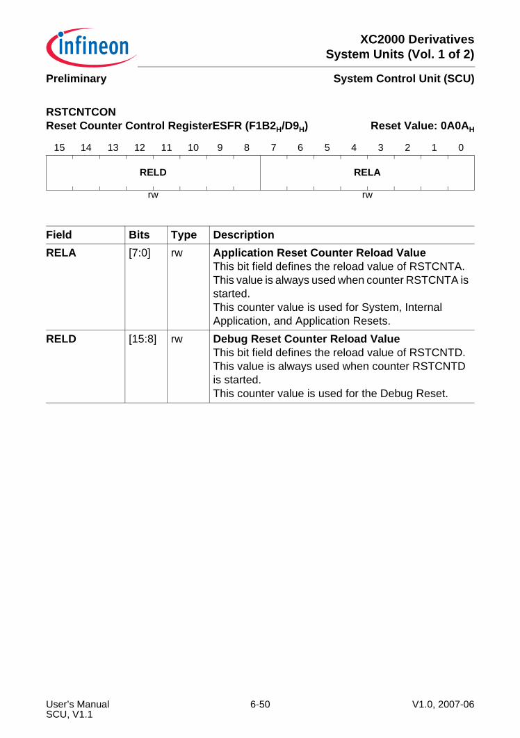
XC2000 DerivativesSystem Units (Vol. 1 of 2)
System Control Unit (SCU)Preliminary
RSTCNTCONReset Counter Control RegisterESFR (F1B2H/D9H) Reset Value: 0A0AH
15 14 13 12 11 10 9 8 7 6 5 4 3 2 1 0
RELD RELA
rw rw
Field Bits Type DescriptionRELA [7:0] rw Application Reset Counter Reload Value
This bit field defines the reload value of RSTCNTA. This value is always used when counter RSTCNTA is started.This counter value is used for System, Internal Application, and Application Resets.
RELD [15:8] rw Debug Reset Counter Reload ValueThis bit field defines the reload value of RSTCNTD. This value is always used when counter RSTCNTD is started.This counter value is used for the Debug Reset.
User’s Manual 6-50 V1.0, 2007-06SCU, V1.1
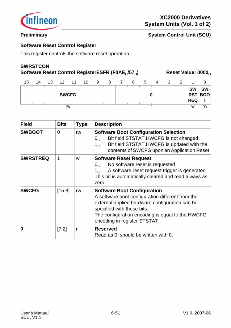
XC2000 DerivativesSystem Units (Vol. 1 of 2)
System Control Unit (SCU)Preliminary
Software Reset Control RegisterThis register controls the software reset operation.
SWRSTCONSoftware Reset Control RegisterESFR (F0AEH/57H) Reset Value: 0000H
15 14 13 12 11 10 9 8 7 6 5 4 3 2 1 0
SWCFG 0SWRSTREQ
SWBOO
Trw r w rw
Field Bits Type DescriptionSWBOOT 0 rw Software Boot Configuration Selection
0B Bit field STSTAT.HWCFG is not changed1B Bit field STSTAT.HWCFG is updated with the
contents of SWCFG upon an Application ResetSWRSTREQ 1 w Software Reset Request
0B No software reset is requested1B A software reset request trigger is generatedThis bit is automatically cleared and read always as zero.
SWCFG [15:8] rw Software Boot ConfigurationA software boot configuration different from the external applied hardware configuration can be specified with these bits.The configuration encoding is equal to the HWCFG encoding in register STSTAT.
0 [7:2] r ReservedRead as 0; should be written with 0.
User’s Manual 6-51 V1.0, 2007-06SCU, V1.1
XC2000 DerivativesSystem Units (Vol. 1 of 2)
System Control Unit (SCU)Preliminary
6.3 External Service Request (ESR) PinsThe ESR pins serve as multi-functional pins for an amount of different options:• Act as reset trigger input• Act as reset output• Act as trap input• Act as stop input for the CapCom60, CapCom61, CapCom62, and CapCom63• Act as wake-up trigger for a power saving mode• Act as trigger input for the GSC• Overlay with other product functions• Independent pad configuration
6.3.1 General OperationEach ESR pin is equipped with an edge detection that allows the selection of the edgesused as triggers. One, both, or non edge can be selected via bit fieldESRCFGx.AEDCON if no clock is active in the application power domain andESRCFGx.SEDCON if a clock is active in the application power domain. Additionallythere a digital (3-stage median) filter (DF) to suppress from spikes. The ESR pin needsto be asserted for a minimum of 2 fSYS clock cycles in order that a trigger is generated.If in the application power domain no clock is active the filter is not taken into account.The filter can be disable by clearing bit ESRCFGx.DFEN.If an ESR trigger is generated please note that triggers for all purposes (reset, trap,CCU6X stop, GSC, and PSC) are generated. If some of the actions resulting out of sucha trigger should not occur this has to be disabled by each feature for its own.The following three figures shows the block diagrams of the three ESR functions.
User’s Manual 6-52 V1.0, 2007-06SCU, V1.1
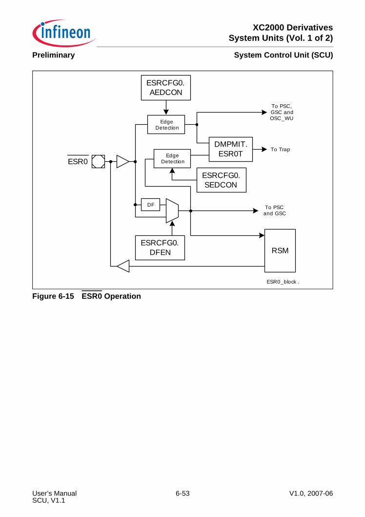
XC2000 DerivativesSystem Units (Vol. 1 of 2)
System Control Unit (SCU)Preliminary
Figure 6-15 ESR0 Operation
RSM
ESR0
ESR0_block .
EdgeDetection
To PSC,GSC andOSC_WU
EdgeDetection
DF
DMPMIT.ESR0T
To Trap
To PSCand GSC
ESRCFG0.SEDCON
ESRCFG0.DFEN
ESRCFG0.AEDCON
User’s Manual 6-53 V1.0, 2007-06SCU, V1.1
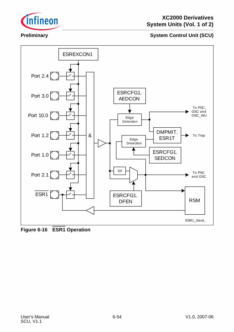
XC2000 DerivativesSystem Units (Vol. 1 of 2)
System Control Unit (SCU)Preliminary
Figure 6-16 ESR1 Operation
RSMESR1
ESR1_block .
EdgeDetection
To PSC,GSC andOSC_WU
EdgeDetection
DF
DMPMIT.ESR1T
To Trap
To PSCand GSC
ESRCFG1.SEDCON
ESRCFG1.DFEN
ESRCFG1.AEDCON
&
Port 2.4
Port 3.0
Port 10.0
Port 1.2
Port 2.1
Port 1.0
ESREXCON1
User’s Manual 6-54 V1.0, 2007-06SCU, V1.1
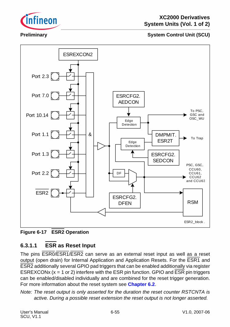
XC2000 DerivativesSystem Units (Vol. 1 of 2)
System Control Unit (SCU)Preliminary
Figure 6-17 ESR2 Operation
6.3.1.1 ESR as Reset InputThe pins ESR0/ESR1/ESR2 can serve as an external reset input as well as a resetoutput (open drain) for Internal Application and Application Resets. For the ESR1 andESR2 additionally several GPIO pad triggers that can be enabled additionally via registerESREXCONx (x = 1 or 2) interfere with the ESR pin function. GPIO and ESR pin triggerscan be enabled/disabled individually and are combined for the reset trigger generation.For more information about the reset system see Chapter 6.2.Note: The reset output is only asserted for the duration the reset counter RSTCNTA is
active. During a possible reset extension the reset output is not longer asserted.
RSM
ESR2
ESR2_block .
EdgeDetection
To PSC,GSC andOSC_WU
EdgeDetection
DF
DMPMIT.ESR2T
To Trap
PSC, GSC,CCU60,CCU61,CCU62
and CCU63
ESRCFG2.SEDCON
ESRCFG2.DFEN
ESRCFG2.AEDCON
&
Port 2.3
Port 7.0
Port 10.14
Port 1.1
Port 2.2
Port 1.3
ESREXCON2
User’s Manual 6-55 V1.0, 2007-06SCU, V1.1
XC2000 DerivativesSystem Units (Vol. 1 of 2)
System Control Unit (SCU)Preliminary
6.3.1.2 ESR as Reset OutputIf the pin ESR0/ESR1/ESR2 is enabled as reset output and the input level is low whilethe output stage is disabled (indicating that it is still driven low externally), the resetcircuitry holds the chip in reset until a high level is detected on ESR0/ESR1/ESR2. Theinternal output stage drives a low level during reset only while RSTCNTA is active. Itdeactivates the output stage when the time defined by RSTCNTCON.RELA has passed.For more information about the reset system see Chapter 6.2.
6.3.1.3 ESR as Trap TriggerThe ESR can request traps. The control mechanism if and which trap is requested islocated in the trap control logic. For more information see Chapter 6.11.3.
6.3.1.4 ESR as Stop InputFor more information see Section 18.10.4.
6.3.1.5 ESR as Wake-up Trigger for the PSCWhen the device is currently in a power save state the ESR pin can be used a wake-uptrigger. For more information see Chapter 6.5.5.
6.3.1.6 ESR as Trigger Input for the GSCThe ESR can be used to request a change in the Control Mode. For more informationsee Chapter 6.6.
6.3.1.7 Overlay with other Product FunctionsFor the pins ESR1 and ESR2 an overlay to other product functions are possible. Forthese two ESR functions additionally other port inputs can be used to generate ESRoperations. This feature can be used for various applications:• Wake-up from a power saving mode on an external Interrupt or CCU6x trigger and
on a CAN or USIC operation• Wake-up from a Clock-off Mode on an external Interrupt or CCU6x trigger and on a
CAN or USIC operation• Request to enter a Clock-off Mode on an external Interrupt or CCU6x trigger and on
a CAN or USIC operationFor information which other peripheral input is on an ESR overlay pin see respectiveData Sheet.For more information about the external interrupt trigger see Chapter 6.4.For more information about the external CCU6x trigger see Section 18.10.4.For more information about CAN operation see Section 20.4.6.
User’s Manual 6-56 V1.0, 2007-06SCU, V1.1
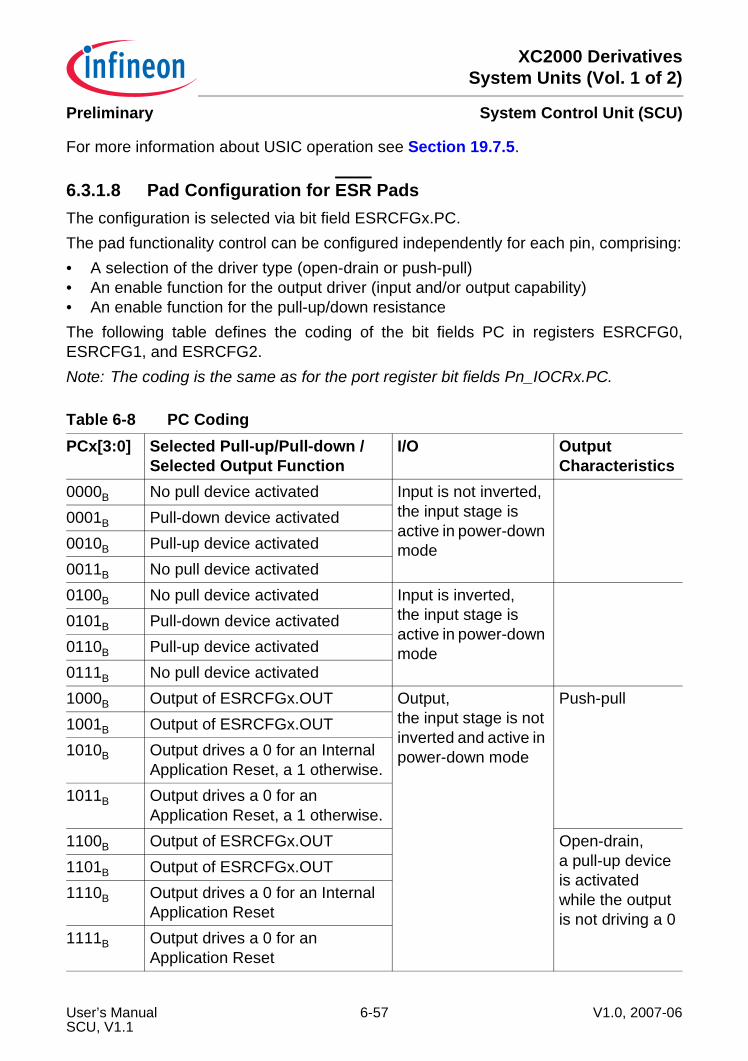
XC2000 DerivativesSystem Units (Vol. 1 of 2)
System Control Unit (SCU)Preliminary
For more information about USIC operation see Section 19.7.5.
6.3.1.8 Pad Configuration for ESR PadsThe configuration is selected via bit field ESRCFGx.PC. The pad functionality control can be configured independently for each pin, comprising:• A selection of the driver type (open-drain or push-pull)• An enable function for the output driver (input and/or output capability)• An enable function for the pull-up/down resistanceThe following table defines the coding of the bit fields PC in registers ESRCFG0,ESRCFG1, and ESRCFG2.Note: The coding is the same as for the port register bit fields Pn_IOCRx.PC.
Table 6-8 PC CodingPCx[3:0] Selected Pull-up/Pull-down /
Selected Output FunctionI/O Output
Characteristics0000B No pull device activated Input is not inverted,
the input stage is active in power-down mode
0001B Pull-down device activated0010B Pull-up device activated0011B No pull device activated0100B No pull device activated Input is inverted,
the input stage is active in power-down mode
0101B Pull-down device activated0110B Pull-up device activated0111B No pull device activated1000B Output of ESRCFGx.OUT Output,
the input stage is not inverted and active in power-down mode
Push-pull1001B Output of ESRCFGx.OUT1010B Output drives a 0 for an Internal
Application Reset, a 1 otherwise.1011B Output drives a 0 for an
Application Reset, a 1 otherwise.1100B Output of ESRCFGx.OUT Open-drain,
a pull-up device is activated while the output is not driving a 0
1101B Output of ESRCFGx.OUT1110B Output drives a 0 for an Internal
Application Reset1111B Output drives a 0 for an
Application Reset
User’s Manual 6-57 V1.0, 2007-06SCU, V1.1
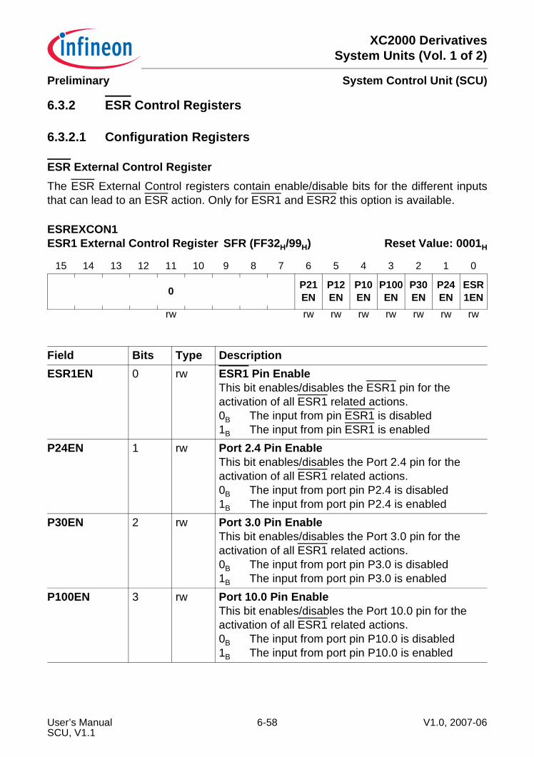
XC2000 DerivativesSystem Units (Vol. 1 of 2)
System Control Unit (SCU)Preliminary
6.3.2 ESR Control Registers
6.3.2.1 Configuration Registers
ESR External Control RegisterThe ESR External Control registers contain enable/disable bits for the different inputsthat can lead to an ESR action. Only for ESR1 and ESR2 this option is available.
ESREXCON1ESR1 External Control Register SFR (FF32H/99H) Reset Value: 0001H
15 14 13 12 11 10 9 8 7 6 5 4 3 2 1 0
0 P21EN
P12EN
P10EN
P100EN
P30EN
P24EN
ESR1EN
rw rw rw rw rw rw rw rw
Field Bits Type DescriptionESR1EN 0 rw ESR1 Pin Enable
This bit enables/disables the ESR1 pin for the activation of all ESR1 related actions.0B The input from pin ESR1 is disabled1B The input from pin ESR1 is enabled
P24EN 1 rw Port 2.4 Pin EnableThis bit enables/disables the Port 2.4 pin for the activation of all ESR1 related actions.0B The input from port pin P2.4 is disabled1B The input from port pin P2.4 is enabled
P30EN 2 rw Port 3.0 Pin EnableThis bit enables/disables the Port 3.0 pin for the activation of all ESR1 related actions.0B The input from port pin P3.0 is disabled1B The input from port pin P3.0 is enabled
P100EN 3 rw Port 10.0 Pin EnableThis bit enables/disables the Port 10.0 pin for the activation of all ESR1 related actions.0B The input from port pin P10.0 is disabled1B The input from port pin P10.0 is enabled
User’s Manual 6-58 V1.0, 2007-06SCU, V1.1
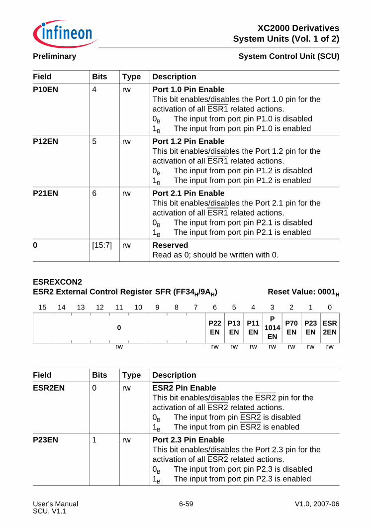
XC2000 DerivativesSystem Units (Vol. 1 of 2)
System Control Unit (SCU)Preliminary
P10EN 4 rw Port 1.0 Pin EnableThis bit enables/disables the Port 1.0 pin for the activation of all ESR1 related actions.0B The input from port pin P1.0 is disabled1B The input from port pin P1.0 is enabled
P12EN 5 rw Port 1.2 Pin EnableThis bit enables/disables the Port 1.2 pin for the activation of all ESR1 related actions.0B The input from port pin P1.2 is disabled1B The input from port pin P1.2 is enabled
P21EN 6 rw Port 2.1 Pin EnableThis bit enables/disables the Port 2.1 pin for the activation of all ESR1 related actions.0B The input from port pin P2.1 is disabled1B The input from port pin P2.1 is enabled
0 [15:7] rw ReservedRead as 0; should be written with 0.
ESREXCON2ESR2 External Control Register SFR (FF34H/9AH) Reset Value: 0001H
15 14 13 12 11 10 9 8 7 6 5 4 3 2 1 0
0 P22EN
P13EN
P11EN
P1014EN
P70EN
P23EN
ESR2EN
rw rw rw rw rw rw rw rw
Field Bits Type DescriptionESR2EN 0 rw ESR2 Pin Enable
This bit enables/disables the ESR2 pin for the activation of all ESR2 related actions.0B The input from pin ESR2 is disabled1B The input from pin ESR2 is enabled
P23EN 1 rw Port 2.3 Pin EnableThis bit enables/disables the Port 2.3 pin for the activation of all ESR2 related actions.0B The input from port pin P2.3 is disabled1B The input from port pin P2.3 is enabled
Field Bits Type Description
User’s Manual 6-59 V1.0, 2007-06SCU, V1.1
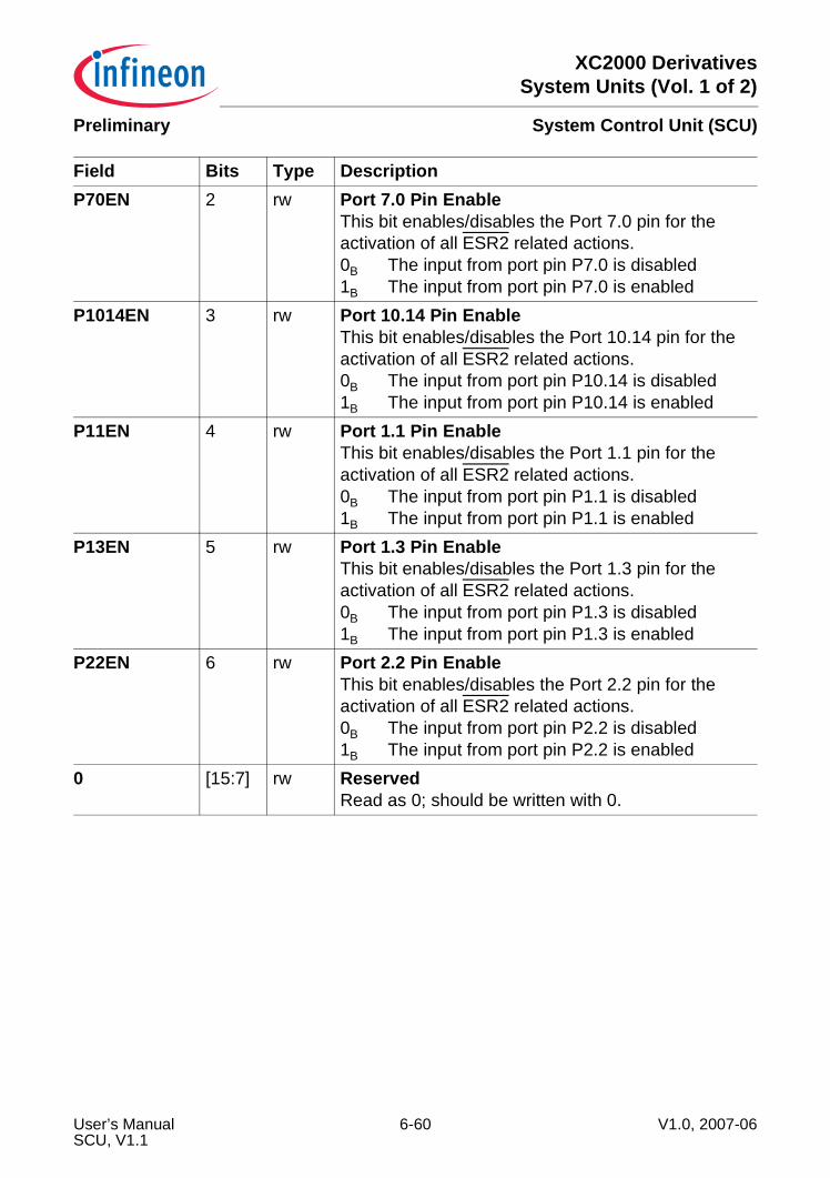
XC2000 DerivativesSystem Units (Vol. 1 of 2)
System Control Unit (SCU)Preliminary
P70EN 2 rw Port 7.0 Pin EnableThis bit enables/disables the Port 7.0 pin for the activation of all ESR2 related actions.0B The input from port pin P7.0 is disabled1B The input from port pin P7.0 is enabled
P1014EN 3 rw Port 10.14 Pin EnableThis bit enables/disables the Port 10.14 pin for the activation of all ESR2 related actions.0B The input from port pin P10.14 is disabled1B The input from port pin P10.14 is enabled
P11EN 4 rw Port 1.1 Pin EnableThis bit enables/disables the Port 1.1 pin for the activation of all ESR2 related actions.0B The input from port pin P1.1 is disabled1B The input from port pin P1.1 is enabled
P13EN 5 rw Port 1.3 Pin EnableThis bit enables/disables the Port 1.3 pin for the activation of all ESR2 related actions.0B The input from port pin P1.3 is disabled1B The input from port pin P1.3 is enabled
P22EN 6 rw Port 2.2 Pin EnableThis bit enables/disables the Port 2.2 pin for the activation of all ESR2 related actions.0B The input from port pin P2.2 is disabled1B The input from port pin P2.2 is enabled
0 [15:7] rw ReservedRead as 0; should be written with 0.
Field Bits Type Description
User’s Manual 6-60 V1.0, 2007-06SCU, V1.1
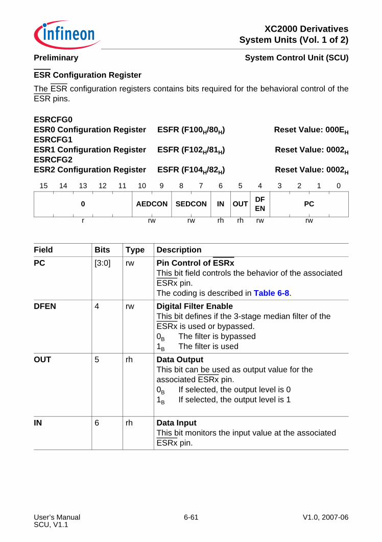
XC2000 DerivativesSystem Units (Vol. 1 of 2)
System Control Unit (SCU)Preliminary
ESR Configuration RegisterThe ESR configuration registers contains bits required for the behavioral control of theESR pins.
ESRCFG0ESR0 Configuration Register ESFR (F100H/80H) Reset Value: 000EHESRCFG1ESR1 Configuration Register ESFR (F102H/81H) Reset Value: 0002HESRCFG2ESR2 Configuration Register ESFR (F104H/82H) Reset Value: 0002H
15 14 13 12 11 10 9 8 7 6 5 4 3 2 1 0
0 AEDCON SEDCON IN OUT DFEN PC
r rw rw rh rh rw rw
Field Bits Type DescriptionPC [3:0] rw Pin Control of ESRx
This bit field controls the behavior of the associated ESRx pin.The coding is described in Table 6-8.
DFEN 4 rw Digital Filter EnableThis bit defines if the 3-stage median filter of the ESRx is used or bypassed.0B The filter is bypassed1B The filter is used
OUT 5 rh Data OutputThis bit can be used as output value for the associated ESRx pin.0B If selected, the output level is 01B If selected, the output level is 1
IN 6 rh Data InputThis bit monitors the input value at the associated ESRx pin.
User’s Manual 6-61 V1.0, 2007-06SCU, V1.1
XC2000 DerivativesSystem Units (Vol. 1 of 2)
System Control Unit (SCU)Preliminary
SEDCON [8:7] rw Synchronous Edge Detection ControlThis bit field defines the edges that lead to an ESRx trigger of the synchronous path.00B No trigger is generated01B A trigger is generated upon a raising edge10B A trigger is generated upon a falling edge11B A trigger is generated upon a raising AND
falling edgeOther combinations than 00B are only allowed if bit field AEDCON is configured to 00B.
AEDCON [10:9] rw Asynchronous Edge Detection ControlThis bit field defines the edges that lead to an ESRx trigger of the asynchronous path.00B No trigger is generated01B A trigger is generated upon a raising edge10B A trigger is generated upon a falling edge11B A trigger is generated upon a raising AND
falling edgeOther combinations than 00B are only allowed if bit field SEDCON is configured to 00B.
0 [15:11] r ReservedRead as 0; should be written with 0.
Field Bits Type Description
User’s Manual 6-62 V1.0, 2007-06SCU, V1.1
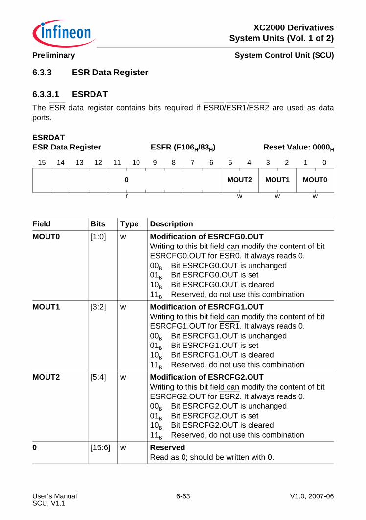
XC2000 DerivativesSystem Units (Vol. 1 of 2)
System Control Unit (SCU)Preliminary
6.3.3 ESR Data Register
6.3.3.1 ESRDATThe ESR data register contains bits required if ESR0/ESR1/ESR2 are used as dataports.
ESRDATESR Data Register ESFR (F106H/83H) Reset Value: 0000H
15 14 13 12 11 10 9 8 7 6 5 4 3 2 1 0
0 MOUT2 MOUT1 MOUT0
r w w w
Field Bits Type DescriptionMOUT0 [1:0] w Modification of ESRCFG0.OUT
Writing to this bit field can modify the content of bit ESRCFG0.OUT for ESR0. It always reads 0.00B Bit ESRCFG0.OUT is unchanged01B Bit ESRCFG0.OUT is set10B Bit ESRCFG0.OUT is cleared11B Reserved, do not use this combination
MOUT1 [3:2] w Modification of ESRCFG1.OUTWriting to this bit field can modify the content of bit ESRCFG1.OUT for ESR1. It always reads 0.00B Bit ESRCFG1.OUT is unchanged01B Bit ESRCFG1.OUT is set10B Bit ESRCFG1.OUT is cleared11B Reserved, do not use this combination
MOUT2 [5:4] w Modification of ESRCFG2.OUTWriting to this bit field can modify the content of bit ESRCFG2.OUT for ESR2. It always reads 0.00B Bit ESRCFG2.OUT is unchanged01B Bit ESRCFG2.OUT is set10B Bit ESRCFG2.OUT is cleared11B Reserved, do not use this combination
0 [15:6] w ReservedRead as 0; should be written with 0.
User’s Manual 6-63 V1.0, 2007-06SCU, V1.1
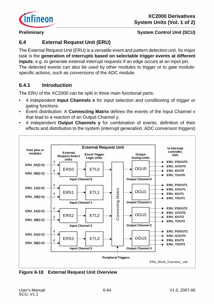
XC2000 DerivativesSystem Units (Vol. 1 of 2)
System Control Unit (SCU)Preliminary
6.4 External Request Unit (ERU)The External Request Unit (ERU) is a versatile event and pattern detection unit. Its majortask is the generation of interrupts based on selectable trigger events at differentinputs, e.g. to generate external interrupt requests if an edge occurs at an input pin.The detected events can also be used by other modules to trigger or to gate module-specific actions, such as conversions of the ADC module.
6.4.1 IntroductionThe ERU of the XC2000 can be split in three main functional parts:• 4 independent Input Channels x for input selection and conditioning of trigger or
gating functions• Event distribution: A Connecting Matrix defines the events of the Input Channel x
that lead to a reaction of an Output Channel y.• 4 independent Output Channels y for combination of events, definition of their
effects and distribution to the system (interrupt generation, ADC conversion triggers)
Figure 6-18 External Request Unit Overview
ERU_Block_Overview_.vsd
ETL0ERS0
4
4 OGU0
ETL1ERS1
4
4
ETL2ERS2
4
4
ETL3ERS3
4
4
ERU_0A[3:0]
ERU_0B[3:0]
Event TriggerLogic Units
ExternalRequest Select
UnitsOutput
Gating Units
to interruptcontroller,
ADC
External Request Unit
Peripheral Triggers
ERU_GOUT0ERU_IOUT0ERU_TOUT0
ERU_PDOUT1
ERU_IOUT1ERU_TOUT1
ERU_PDOUT2
ERU_IOUT2ERU_TOUT2
ERU_PDOUT3
ERU_IOUT3ERU_TOUT3
Con
nect
ing
Mat
rix
ERU_1A[3:0]
ERU_1B[3:0]
ERU_2A[3:0]
ERU_2B[3:0]
ERU_3A[3:0]
ERU_3B[3:0]
from pins ormodules
ERU_PDOUT0
OGU3
OGU2
OGU1ERU_GOUT1
ERU_GOUT2
ERU_GOUT3
Input Channel 0
Input Channel 1
Input Channel 2
Input Channel 3 Output Channel 3
Output Channel 2
Output Channel 1
Output Channel 0
User’s Manual 6-64 V1.0, 2007-06SCU, V1.1
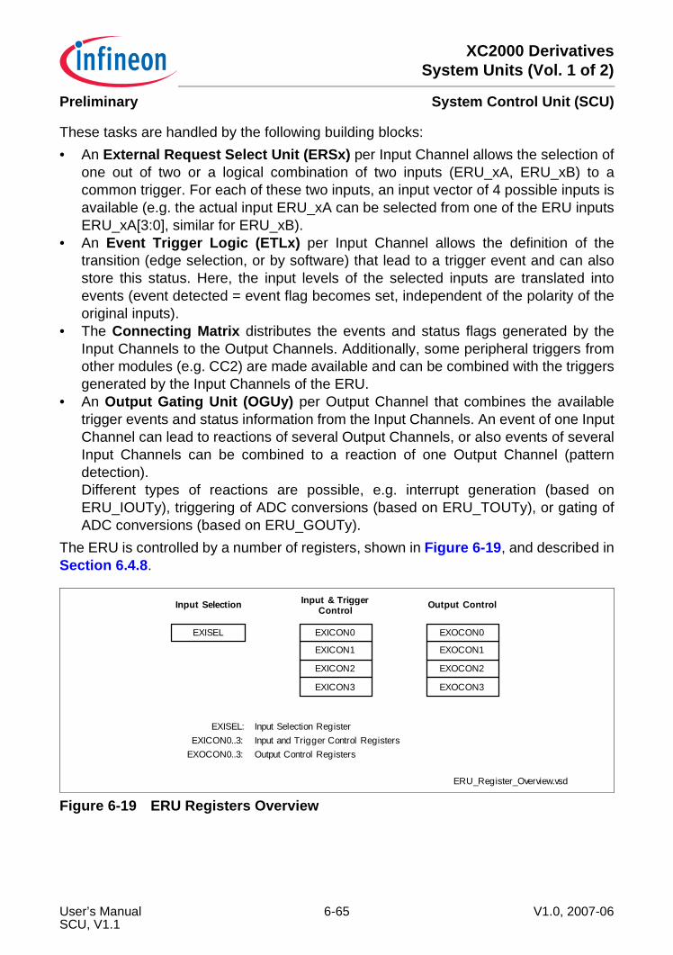
XC2000 DerivativesSystem Units (Vol. 1 of 2)
System Control Unit (SCU)Preliminary
These tasks are handled by the following building blocks:• An External Request Select Unit (ERSx) per Input Channel allows the selection of
one out of two or a logical combination of two inputs (ERU_xA, ERU_xB) to acommon trigger. For each of these two inputs, an input vector of 4 possible inputs isavailable (e.g. the actual input ERU_xA can be selected from one of the ERU inputsERU_xA[3:0], similar for ERU_xB).
• An Event Trigger Logic (ETLx) per Input Channel allows the definition of thetransition (edge selection, or by software) that lead to a trigger event and can alsostore this status. Here, the input levels of the selected inputs are translated intoevents (event detected = event flag becomes set, independent of the polarity of theoriginal inputs).
• The Connecting Matrix distributes the events and status flags generated by theInput Channels to the Output Channels. Additionally, some peripheral triggers fromother modules (e.g. CC2) are made available and can be combined with the triggersgenerated by the Input Channels of the ERU.
• An Output Gating Unit (OGUy) per Output Channel that combines the availabletrigger events and status information from the Input Channels. An event of one InputChannel can lead to reactions of several Output Channels, or also events of severalInput Channels can be combined to a reaction of one Output Channel (patterndetection).Different types of reactions are possible, e.g. interrupt generation (based onERU_IOUTy), triggering of ADC conversions (based on ERU_TOUTy), or gating ofADC conversions (based on ERU_GOUTy).
The ERU is controlled by a number of registers, shown in Figure 6-19, and described inSection 6.4.8.
Figure 6-19 ERU Registers Overview
ERU_Register_Overview.vsd
Output Control
EXISEL
EXICON1
EXICON0
EXICON2
EXICON3
Input Selection Input & TriggerControl
EXISEL: Input Selection RegisterEXICON0..3: Input and Trigger Control Registers
EXOCON1
EXOCON0
EXOCON2
EXOCON3
EXOCON0..3: Output Control Registers
User’s Manual 6-65 V1.0, 2007-06SCU, V1.1

XC2000 DerivativesSystem Units (Vol. 1 of 2)
System Control Unit (SCU)Preliminary
6.4.2 ERU Pin ConnectionsFigure 6-20 shows the ERU input connections, either directly with pins or viacommunication modules, such as USIC or MultiCAN. These communication modulesprovide their inputs (e.g. CAN receive input, or USIC data, clock, or control inputs) thathave been selected in these modules. With this structure, the number of possible inputpins is significantly increased, because not only the selection capability of the ERU isused, but also the selection capability of the communication modules.
Figure 6-20 ERU Inputs Overview
The inputs to the ERU can be selected from a large number of inputs. While some of theinputs come directly from a pin, other inputs come from various peripheral modules, such
ERU_Inputs_Overview.vsd
ERS0ERU_0A0
ERU_0A1
ERU_0A2
ERU_0A3
ERU_0B0
ERU_0B1
ERU_0B2
ERU_0B3
ESR1
ERU_1A0
ERU_1A1
ERU_1A2
ERU_1A3
ERU_1B0
ERU_1B1
ERU_1B2
ERU_1B3
P2.1
P1.0
P5.13
P2.2
P1.1
ESR2
ERU_2A0
ERU_2A1
ERU_2A2
ERU_2A3
ERU_2B0
ERU_2B1
ERU_2B2
ERU_2B3
MultiCAN_CAN3INS,selected receive input CAN3
ERU_3A0
ERU_3A1
ERU_3A2
ERU_3A3
ERU_3B0
ERU_3B1
ERU_3B2
ERU_3B3
P1.2 P1.3
reserved
reserved
reserved
reserved
ERS1
ERS2 ERS3
U1C0_DX0INS,selected data input
U1C0_DX2INS,selected control input
U1C1_DX0INS,selected data input
U1C1_DX2INS,selected control input
U0C0_DX0INS,selected data input
U0C0_DX2INS,selected control input
U0C1_DX0INS,selected data input
U0C1_DX2INS,selected control input
U2C0_DX0INS,selected data input
U2C0_DX2INS,selected control input
U2C1_DX0INS,selected data input
U2C1_DX2INS,selected control input
U2C0_DX1INS,selected clock input
U1C0_DX1INS,selected clock input
MultiCAN_CAN2INS,selected receive input CAN2
MultiCAN_CAN0INS,selected receive input CAN0
MultiCAN_CAN1INS,selected receive input CAN1
MultiCAN_CAN4INS,selected receive input CAN4
User’s Manual 6-66 V1.0, 2007-06SCU, V1.1
XC2000 DerivativesSystem Units (Vol. 1 of 2)
System Control Unit (SCU)Preliminary
as the USIC (inputs named with prefix UxCy to indicate which the communicationchannel) and the MultiCAN modules. These inputs come from the pins that has beenselected as inputs for a USIC or MultiCAN function. The selection of the input is madewithin the respective USIC or MultiCAN module.Usually, such inputs would be selected for an ERU function when the input function tothe USIC or MultiCAN module is not used otherwise, or the module is not used at all.However, it is also possible to select a input that is actually needed in a USIC orMultiCAN module, and to use it also in the ERU to provide for certain trigger functions,eventually combined with other inputs (e.g. to generate an interrupt in case a start offrame is detected at a selected communication input).Table 6-9 provides a complete overview of all pins as well as the ESRx inputs, that canpossibly be used as inputs to the ERU. Please note that there are also some otherperipheral inputs, that can be selected by the USIC or MultiCAN module via theirrespective input multiplexers, and that can therefore be used as ERU inputs.In total, external inputs from up to 51 pins (from which 7 are direct inputs to the ERU)plus the ESRx pins can be chosen. For some of them, several choices exist in respectto which module provides it and to which ERSx they are connected to).
Table 6-9 ERU External Pin Input Options
Port Pin Selectable via ERU InputP0 P0.0 U1C0 data input DX0A ERS1, ERU_1A2
P0.1 U1C0 data input DX0BU1C0 clock input DX1A
ERS1, ERU_1A2ERS3, ERU_3B0
P0.2 U1C0 clock input DX1B ERS3, ERU_3B0P0.3 U1C0 control input DX2A
MultiCAN receive input RXDC0BERS1, ERU_1A3ERS3, ERU_3B1
P0.4 U1C1 control input DX2AMultiCan receive input RXDC1B
ERS1, ERU_1B3ERS3, ERU_3A1
P0.5 U1C0 clock input DX1C ERS3, ERU_3B0P0.5 U1C1 data input DX0A ERS1, ERU_1B2P0.7 U1C1 data input DX0B ERS1, ERU_1B2
User’s Manual 6-67 V1.0, 2007-06SCU, V1.1
XC2000 DerivativesSystem Units (Vol. 1 of 2)
System Control Unit (SCU)Preliminary
P1 P1.0 Direct ERU input ERS0, ERU_0B0P1.1 Direct ERU input
U2C1 data input DX0CERS1, ERU_1B0ERS2, ERU_2B2
P1.2 Direct ERU inputU2C1 data input DX0D
ERS2, ERU_2A0ERS2, ERU_2B2
P1.3 Direct ERU input ERS3, ERU_3A0P1.4 U2C0 control input DX2B ERS2, ERU_2A3P1.5 U2C0 data input DX0C ERS2, ERU_2A2P1.6 U2C0 data input DX0D ERS2, ERU_2A2P1.7 U2C0 clock input DX1C ERS2, ERU_2B0
P2 P2.0 MultiCAN receive input RXDC0C ERS3, ERU_3B1P2.1 Direct ERU input ERS0, ERU_0A0P2.2 Direct ERU input ERS1, ERU_1A0
P2 P2.3 U0C0 data input DX0EMultiCAN receive input RXDC0A
ERS0, ERU_0A2ERS3, ERU_3B1
P2.4 U0C0 data input DX0FMultiCAN receive input RXDC1A
ESR0, ERU_0A2ERS3, ERU_3A1
P2.6 U0C0 control input DX2DMultiCAN receive input RXDC0D
ERS0, ERU_0A3ERS3, ERU_3B1
P2.7 U0C1 control input DX2CMultiCAN receive input RXDC1C
ERS0, ERU_0B3ERS3, ERU_3A1
P2.10 U0C1 data input DX0E ERS0, ERU_0B2P3 P3.0 U2C0 data input DX0A
U2C0 clock input DX1AMultiCAN receive input RXDC3B
ERS2, ERU_2A2ERS2, ERU_2B0ERS2, ERU_2A1
P3.1 U2C0 data input DX0B ERS2, ERU_2A2P3.2 U2C0 control input DX2A
U2C0 clock input DX1BERS2, ERU_2A3ERS2, ERU_2B0
P3.3 MultiCAN receive input RXDC3A ERS2, ERU_2A1P3.4 U2C1 control input DX2A
MultiCAN receive input RXDC4AERS2, ERU_2B3ERS1, ERU_1B1
P3.6 U2C1 data input DX0A ERS2, ERU_2B2P3.7 U2C0 data input DX0B ERS2, ERU_2B2
Table 6-9 ERU External Pin Input Options (cont’d)
Port Pin Selectable via ERU Input
User’s Manual 6-68 V1.0, 2007-06SCU, V1.1

XC2000 DerivativesSystem Units (Vol. 1 of 2)
System Control Unit (SCU)Preliminary
P4 P4.3 MultiCAN receive input RXDC2A ERS2, ERU_2B1P5 P5.13 Direct ERU input ERS0, ERU_0B1P6 P6.0 U1C1 data input DX0E ERS1, ERU_1B2
P6.3 U1C1 control input DX2D ERS1, ERU_1B3P7 P7.0 MultiCAN Node 4 receive input RXDC4B ERS1, ERU_1B1
P7.3 U0C1 data input DX0F ERS0, ERU_0B2P7.4 U0C0 data input DX0D ERS0, ERU_0A2
P9 P9.5 U2C0 data input DX0D ERS2, ERU_2A2P9.7 U2C0 clock input DX1D ERS2, ERU_2B0
P10 P10.0 U0C0 data input DX0AU0C1 data input DX0A
ERS0, ERU_0A2ERS0, ERU_0B2
P10.1 U0C0 data input DX0B ERS0, ERU_0A2P10 P10.3 U0C0 control input DX2A
U0C1 control input DX2AERS0, ERU_0A3ERS0, ERU_0B3
P10.4 U0C0 control input DX2BU0C1 control input DX2B
ERS0, ERU_0A3ERS0, ERU_0B3
P10.6 U0C0 data input DX0CU1C0 control input DX2D
ERS0, ERU_0A2ERS1, ERU_1A3
P10.7 U0C1 data input DX0BMultiCAN receive input RXDC4C
ERS0, ERU_0B2ERS1, ERU_1B1
P10.10 U0C 0 control input DX2C ERS0, ERU_0A3P10.11 U1C0 clock input DX1D
MultiCAN receive input RXDC2BERS3, ERU_3B0ERS2, ERU_2B1
P10.12 U1C0 data input DX0CU1C0 clock input DX1D
ERS1, ERU_1A2ERS3, ERU_3B0
P10.13 U1C0 data input DX0D ERS1, ERU_1A2P10.14 U0C1 data input DX0C
MultiCAN receive input RXDC3CERS0, ERU_0B2ERS2, ERU_2A1
Table 6-9 ERU External Pin Input Options (cont’d)
Port Pin Selectable via ERU Input
User’s Manual 6-69 V1.0, 2007-06SCU, V1.1
XC2000 DerivativesSystem Units (Vol. 1 of 2)
System Control Unit (SCU)Preliminary
ESRinputs
ESR0 U1C0 data input DX0EU1C0 control input DX2BMultiCAN receive input RXDC2D
ERS1, ERU_1A2ERS1, ERU_1A3ERS2, ERU_2B1
ESR1 Direct ERU inputU1C0 data input DX0FU1C0 control input DX2CU1C1 data input DX0CU1C1 control input DX2BU2C0 data input DX0FU2C1 control input DX2CMultiCAN receive input RXDC0E
ERS0, ERU_0A1ERS1, ERU_1A2ERS1, ERU_1A3ERS1, ERU_1B2ERS1, ERU_1B3ERS2, ERU_2B2ERS2, ERU_2B3ERS3, ERU_3B1
ESR2 Direct ERU inputU1C1 data input DX0DU1C1 control input DX2CU2C0 data input DX0EU2C1 control input DX2BMultiCAN receive input RXDC1E
ERS1, ERU_1A1ERS1, ERU_1B2ERS1, ERU_1B3ERS2, ERU_2B2ERS2, ERU_2B3ERS3, ERU_3A1
Table 6-9 ERU External Pin Input Options (cont’d)
Port Pin Selectable via ERU Input
User’s Manual 6-70 V1.0, 2007-06SCU, V1.1
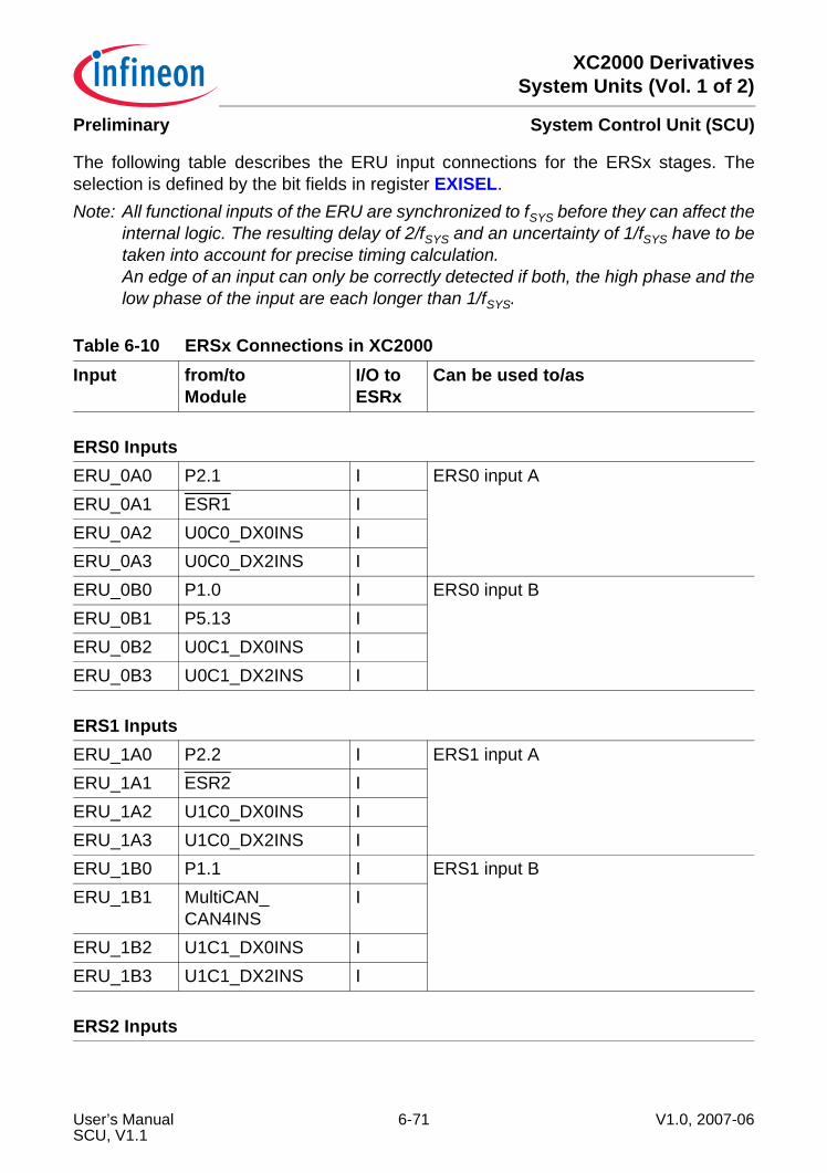
XC2000 DerivativesSystem Units (Vol. 1 of 2)
System Control Unit (SCU)Preliminary
The following table describes the ERU input connections for the ERSx stages. Theselection is defined by the bit fields in register EXISEL.Note: All functional inputs of the ERU are synchronized to fSYS before they can affect the
internal logic. The resulting delay of 2/fSYS and an uncertainty of 1/fSYS have to betaken into account for precise timing calculation.An edge of an input can only be correctly detected if both, the high phase and thelow phase of the input are each longer than 1/fSYS.
Table 6-10 ERSx Connections in XC2000Input from/to
ModuleI/O to ESRx
Can be used to/as
ERS0 InputsERU_0A0 P2.1 I ERS0 input AERU_0A1 ESR1 IERU_0A2 U0C0_DX0INS IERU_0A3 U0C0_DX2INS IERU_0B0 P1.0 I ERS0 input BERU_0B1 P5.13 IERU_0B2 U0C1_DX0INS IERU_0B3 U0C1_DX2INS I
ERS1 InputsERU_1A0 P2.2 I ERS1 input AERU_1A1 ESR2 IERU_1A2 U1C0_DX0INS IERU_1A3 U1C0_DX2INS IERU_1B0 P1.1 I ERS1 input BERU_1B1 MultiCAN_
CAN4INSI
ERU_1B2 U1C1_DX0INS IERU_1B3 U1C1_DX2INS I
ERS2 Inputs
User’s Manual 6-71 V1.0, 2007-06SCU, V1.1

XC2000 DerivativesSystem Units (Vol. 1 of 2)
System Control Unit (SCU)Preliminary
6.4.3 External Request Select Unit (ERSx; x = 0..3)For each Input Channel x, an ERSx unit handles the input selection for the associatedETLx unit. Each ERSx performs a logical combination of two inputs (Ax, Bx) to provideone combined output ERSxO to the associated ETLx. Input Ax can be selected from 4possibilities of the input vector ERU_xA[3:0] and can be optionally inverted. A similarstructure exists for input Bx (selection from ERU_xB[3:0]).In addition to the direct choice of either input Ax or Bx or their inverted values, thepossible logical combinations for two selected inputs are a logical AND or a logical OR.
ERU_2A0 P1.2 I ERS2 input AERU_2A1 MultiCAN_
CAN3INSI
ERU_2A2 U2C0_DX0INS IERU_2A3 U2C0_DX2INS IERU_2B0 U2C0_DX1INS I ERS2 input BERU_2B1 MultiCAN_
CAN2INSI
ERU_2B2 U2C1_DX0INS IERU_2B3 U2C1_DX2INS I
ERS3 InputsERU_3A0 P1.3 I ERS3 input AERU_3A1 MultiCAN_
CAN1INSI
ERU_3A2 0 IERU_3A3 0 IERU_3B0 U1C0_DX1INS I ERS3 input BERU_3B1 MultiCAN_
CAN0INSI
ERU_3B2 0 IERU_3B3 0 I
Table 6-10 ERSx Connections in XC2000 (cont’d)
Input from/toModule
I/O to ESRx
Can be used to/as
User’s Manual 6-72 V1.0, 2007-06SCU, V1.1

XC2000 DerivativesSystem Units (Vol. 1 of 2)
System Control Unit (SCU)Preliminary
Figure 6-21 External Request Select Unit Overview
The ERS units are controlled via register EXISEL (one register for all four ERSx units)and registers EXICONx (one register for each ERSx and associated ETLx unit, e.g.EXICON0 for Input Channel 0).
ERU_ERS.vsd
ETLx
External RequestSelect Unit x (ERSx)
Ax
Bx
Ax AND Bx
Ax OR Bx
ERU_xA0
ERU_xA1
ERU_xA2
ERU_xA3
ERU_xB0
ERU_xB1
ERU_xB2
ERU_xB3
ERSxO
&
1
SelectInputAx
SelectInputBx
EXISEL.EXSxB
EXISEL.EXSxA
SelectPolarity
Ax
EXICONx.NA
SelectPolarity
Bx
EXICONx.NB
SelectSource
forERSxO
EXICONx.SS
User’s Manual 6-73 V1.0, 2007-06SCU, V1.1
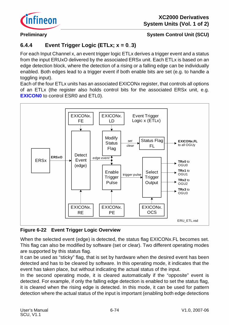
XC2000 DerivativesSystem Units (Vol. 1 of 2)
System Control Unit (SCU)Preliminary
6.4.4 Event Trigger Logic (ETLx; x = 0..3)For each Input Channel x, an event trigger logic ETLx derives a trigger event and a statusfrom the input ERUxO delivered by the associated ERSx unit. Each ETLx is based on anedge detection block, where the detection of a rising or a falling edge can be individuallyenabled. Both edges lead to a trigger event if both enable bits are set (e.g. to handle atoggling input).Each of the four ETLx units has an associated EXICONx register, that controls all optionsof an ETLx (the register also holds control bits for the associated ERSx unit, e.g.EXICON0 to control ESR0 and ETL0).
Figure 6-22 Event Trigger Logic Overview
When the selected event (edge) is detected, the status flag EXICONx.FL becomes set.This flag can also be modified by software (set or clear). Two different operating modesare supported by this status flag.It can be used as “sticky” flag, that is set by hardware when the desired event has beendetected and has to be cleared by software. In this operating mode, it indicates that theevent has taken place, but without indicating the actual status of the input.In the second operating mode, it is cleared automatically if the “opposite” event isdetected. For example, if only the falling edge detection is enabled to set the status flag,it is cleared when the rising edge is detected. In this mode, it can be used for patterndetection where the actual status of the input is important (enabling both edge detections
ERU_ETL.vsd
setclear
Event Trigger Logic x (ETLx)
TRx0 toOGU0
EXICONx.FLto all OGUy
ERSxOERSx
DetectEvent(edge)
EXICONx.FE
EXICONx.RE
trigger pulse
Status FlagFL
ModifyStatusFlag
EXICONx.LD
EXICONx.PE
SelectTriggerOutput
EXICONx.OCS
EnableTriggerPulse
TRx1 toOGU1
TRx2 toOGU2
TRx3 toOGU3
edge event
User’s Manual 6-74 V1.0, 2007-06SCU, V1.1
XC2000 DerivativesSystem Units (Vol. 1 of 2)
System Control Unit (SCU)Preliminary
is not useful in this mode).The output of the status flag is connected to all following Output Gating Units (OGUy) inparallel (see Figure 6-23) to provide pattern detection capability of all OGUy unitsbased on different or the same status flags.In addition to the modification of the status flag, a trigger pulse output TRxy of ETLx canbe enabled (by bit EXICONx.PE) and selected to trigger actions in one of the OGUyunits. The target OGUy for the trigger is selected by bit field EXICON.OCS.The trigger becomes active when the selected edge event is detected, independentlyfrom the status flag EXICONx.FL.
User’s Manual 6-75 V1.0, 2007-06SCU, V1.1
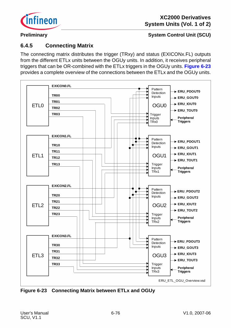
XC2000 DerivativesSystem Units (Vol. 1 of 2)
System Control Unit (SCU)Preliminary
6.4.5 Connecting MatrixThe connecting matrix distributes the trigger (TRxy) and status (EXICONx.FL) outputsfrom the different ETLx units between the OGUy units. In addition, it receives peripheraltriggers that can be OR-combined with the ETLx triggers in the OGUy units. Figure 6-23provides a complete overview of the connections between the ETLx and the OGUy units.
Figure 6-23 Connecting Matrix between ETLx and OGUy
OGU0
ERU_ETL_OGU_Overview.vsd
ETL0
ETL1
ETL2
ETL3
TR00
TR01
TR02
TR03
EXICON0.FL
TR10
TR11
TR12
TR13
EXICON1.FL
TR20
TR21
TR22
TR23
EXICON2.FL
TR30
TR31
TR32
TR33
EXICON3.FL
PatternDetectionInputs
TriggerInputsTRx0
OGU1
PatternDetectionInputs
TriggerInputsTRx1
OGU3
PatternDetectionInputs
TriggerInputsTRx3
OGU2
PatternDetectionInputs
TriggerInputsTRx2
PeripheralTriggers
ERU_IOUT3
ERU_TOUT3
ERU_PDOUT3
ERU_IOUT2
ERU_TOUT2
ERU_PDOUT2
ERU_IOUT1
ERU_TOUT1
ERU_PDOUT1
ERU_IOUT0
ERU_TOUT0
ERU_PDOUT0
PeripheralTriggers
PeripheralTriggers
PeripheralTriggers
ERU_GOUT0
ERU_GOUT1
ERU_GOUT2
ERU_GOUT3
User’s Manual 6-76 V1.0, 2007-06SCU, V1.1
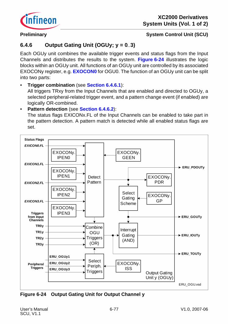
XC2000 DerivativesSystem Units (Vol. 1 of 2)
System Control Unit (SCU)Preliminary
6.4.6 Output Gating Unit (OGUy; y = 0..3)Each OGUy unit combines the available trigger events and status flags from the InputChannels and distributes the results to the system. Figure 6-24 illustrates the logicblocks within an OGUy unit. All functions of an OGUy unit are controlled by its associatedEXOCONy register, e.g. EXOCON0 for OGU0. The function of an OGUy unit can be splitinto two parts:• Trigger combination (see Section 6.4.6.1):
All triggers TRxy from the Input Channels that are enabled and directed to OGUy, aselected peripheral-related trigger event, and a pattern change event (if enabled) arelogically OR-combined.
• Pattern detection (see Section 6.4.6.2):The status flags EXICONx.FL of the Input Channels can be enabled to take part inthe pattern detection. A pattern match is detected while all enabled status flags areset.
Figure 6-24 Output Gating Unit for Output Channel y
ERU_OGU.vsd
Output GatingUnit y (OGUy)
ERU_OGUy1
EXICON1.FL
TR0y
TR1y
TR2y
TR3y
ERU_PDOUTy
DetectPattern
EXOCONy.IPEN1
EXICON2.FL
EXOCONy.IPEN2
EXICON3.FL
EXOCONy.IPEN3
EXICON0.FL
EXOCONy.IPEN0
EXOCONy.PDR
EXOCONy.GEEN
CombineOGU
Triggers(OR)
SelectPeriph.Triggers
ERU_OGUy2
ERU_OGUy3EXOCONy.
ISS
SelectGating
Scheme
EXOCONy.GP
ERU_GOUTy
ERU_IOUTy
ERU_TOUTy
PeripheralTriggers
Triggersfrom InputChannels
Status Flags
InterruptGating(AND)
User’s Manual 6-77 V1.0, 2007-06SCU, V1.1
XC2000 DerivativesSystem Units (Vol. 1 of 2)
System Control Unit (SCU)Preliminary
Each OGUy units generates 4 outputs that are distributed to the system (not all of themare necessarily used, please refer to Section 6.4.7):• ERU_PDOUTy to directly output the pattern match information for gating purposes
in other modules (pattern match = 1).• ERU_GOUTy to output the pattern match or pattern miss information (inverted
pattern match), or a permanent 0 or 1 under software control for gating purposes inother modules.
• ERU_TOUTy as combination of a peripheral trigger, a pattern detection resultchange event, or the ETLx trigger outputs TRxy to trigger actions in other modules.
• ERU_IOUTy as gated trigger output (ERU_GOUTy logical AND-combined withERU_TOUTy) to trigger interrupts (e.g. the interrupt generation can be gated to allowinterrupt activation during a certain time window).
6.4.6.1 Trigger CombinationThe trigger combination logically OR-combines different trigger inputs to form a commontrigger ERU_TOUTy. Possible trigger inputs are:• In each ETLx unit of the Input Channels, the trigger output TRxy can be enabled and
the trigger event can be directed to one of the OGUy units.• One out of three peripheral triggers per OGUy can be selected as additional trigger
source. These peripheral triggers are generated by on-chip peripheral modules, suchas capture/compare or timer units. The selection is done by bit field EXOCONy.ISS.
• In the case that at least one pattern detection input is enabled (EXOCONy.IPENx)and a change of the pattern detection result from pattern match to pattern miss (orvice-versa) is detected, a trigger event is generated to indicate a pattern detectionresult event (if enabled by ECOCONy.GEEN).
The trigger combination offers the possibility to program different trigger criteria forseveral inputs (independently for each Input Channel) or peripheral triggers, and tocombine their effects to a single output, e.g. to generate an interrupt or to start an ADCconversion. This combination capability allows the generation of an interrupt per OGUthat can be triggered by several inputs (multitude of request sources -> one reaction).The following table describes the peripheral trigger connections for the OGUy stages.The selection is defined by the bit fields ISS in registers EXOCON0 (for OGU0),EXOCON1 (for OGU1), EXOCON2 (for OGU2), or EXOCON3 (for OGU3).
User’s Manual 6-78 V1.0, 2007-06SCU, V1.1
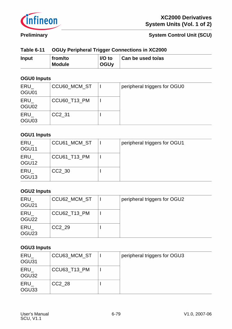
XC2000 DerivativesSystem Units (Vol. 1 of 2)
System Control Unit (SCU)Preliminary
Table 6-11 OGUy Peripheral Trigger Connections in XC2000Input from/to
ModuleI/O to OGUy
Can be used to/as
OGU0 InputsERU_OGU01
CCU60_MCM_ST I peripheral triggers for OGU0
ERU_OGU02
CCU60_T13_PM I
ERU_OGU03
CC2_31 I
OGU1 InputsERU_OGU11
CCU61_MCM_ST I peripheral triggers for OGU1
ERU_OGU12
CCU61_T13_PM I
ERU_OGU13
CC2_30 I
OGU2 InputsERU_OGU21
CCU62_MCM_ST I peripheral triggers for OGU2
ERU_OGU22
CCU62_T13_PM I
ERU_OGU23
CC2_29 I
OGU3 InputsERU_OGU31
CCU63_MCM_ST I peripheral triggers for OGU3
ERU_OGU32
CCU63_T13_PM I
ERU_OGU33
CC2_28 I
User’s Manual 6-79 V1.0, 2007-06SCU, V1.1
XC2000 DerivativesSystem Units (Vol. 1 of 2)
System Control Unit (SCU)Preliminary
6.4.6.2 Pattern DetectionThe pattern detection logic allows the combination of the status flags of all ETLx units.Each status flag can be individually included or excluded from the pattern detection foreach OGUy, via control bits EXOCONy.IPENx. The pattern detection block outputs thefollowing pattern detection results:• Pattern match (EXOCONy.PDR = 1 and ERU_PDOUTy = 1):
A pattern match is indicated while all status flags FL that are included in the patterndetection are 1.
• Pattern miss (EXOCONy.PDR = 0 and ERU_PDOUTy = 0):A pattern miss is indicated while at least one of the status flags FL that are includedin the pattern detection is 0.
In addition, the pattern detection can deliver a trigger event if the pattern detection resultchanges from match to miss or vice-versa (if enabled by EXOCONy.GEEN = 1). Thepattern result change event is logically OR-combined with the other enabled triggerevents to support interrupt generation or to trigger other module functions (e.g. in theADC). The event is indicated when the pattern detection result changes andEXOCONy.PDR becomes updated.The interrupt generation in the OGUy is based on the trigger ERU_TOUTy that can begated (masked) with the pattern detection result ERU_PDOUTy. This allows anautomatic and reproducible generation of interrupts during a certain time window, wherethe request event is elaborated by the trigger combination block and the time windowinformation (gating) is given by the pattern detection. For example, interrupts can beissued on a regular time base (peripheral trigger input from capture/compare unit isselected) while a combination of inputs occurs (pattern detection based on ETLx statusbits).A programmable gating scheme introduces flexibility to adapt to applicationrequirements and allows the generation of interrupt requests ERU_IOUTy underdifferent conditions:• Pattern match (EXOCONy.GP = 10B):
An interrupt request is issued when a trigger event occurs while the pattern detectionshows a pattern match.
• Pattern miss (EXOCONy.GP = 11B):An interrupt request is issued when the trigger event occurs while the patterndetection shows a pattern miss.
• Independent of pattern detection (EXOCONy.GP = 01B):In this mode, each occurring trigger event leads to an interrupt request. The patterndetection output can be used independently from the trigger combination for gatingpurposes of other peripherals (independent use of ERU_TOUTy and ERU_PDOUTywith interrupt requests on trigger events).
• No interrupts (EXOCONy.GP = 00B, default setting)In this mode, an occurring trigger event does not lead to an interrupt request. The
User’s Manual 6-80 V1.0, 2007-06SCU, V1.1
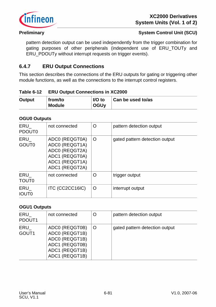
XC2000 DerivativesSystem Units (Vol. 1 of 2)
System Control Unit (SCU)Preliminary
pattern detection output can be used independently from the trigger combination forgating purposes of other peripherals (independent use of ERU_TOUTy andERU_PDOUTy without interrupt requests on trigger events).
6.4.7 ERU Output ConnectionsThis section describes the connections of the ERU outputs for gating or triggering othermodule functions, as well as the connections to the interrupt control registers.
Table 6-12 ERU Output Connections in XC2000Output from/to
ModuleI/O to OGUy
Can be used to/as
OGU0 OutputsERU_PDOUT0
not connected O pattern detection output
ERU_GOUT0
ADC0 (REQGT0A)ADC0 (REQGT1A)ADC0 (REQGT2A)ADC1 (REQGT0A)ADC1 (REQGT1A)ADC1 (REQGT2A)
O gated pattern detection output
ERU_TOUT0
not connected O trigger output
ERU_IOUT0
ITC (CC2CC16IC) O interrupt output
OGU1 OutputsERU_PDOUT1
not connected O pattern detection output
ERU_GOUT1
ADC0 (REQGT0B)ADC0 (REQGT1B)ADC0 (REQGT1B)ADC1 (REQGT0B)ADC1 (REQGT1B)ADC1 (REQGT1B)
O gated pattern detection output
User’s Manual 6-81 V1.0, 2007-06SCU, V1.1
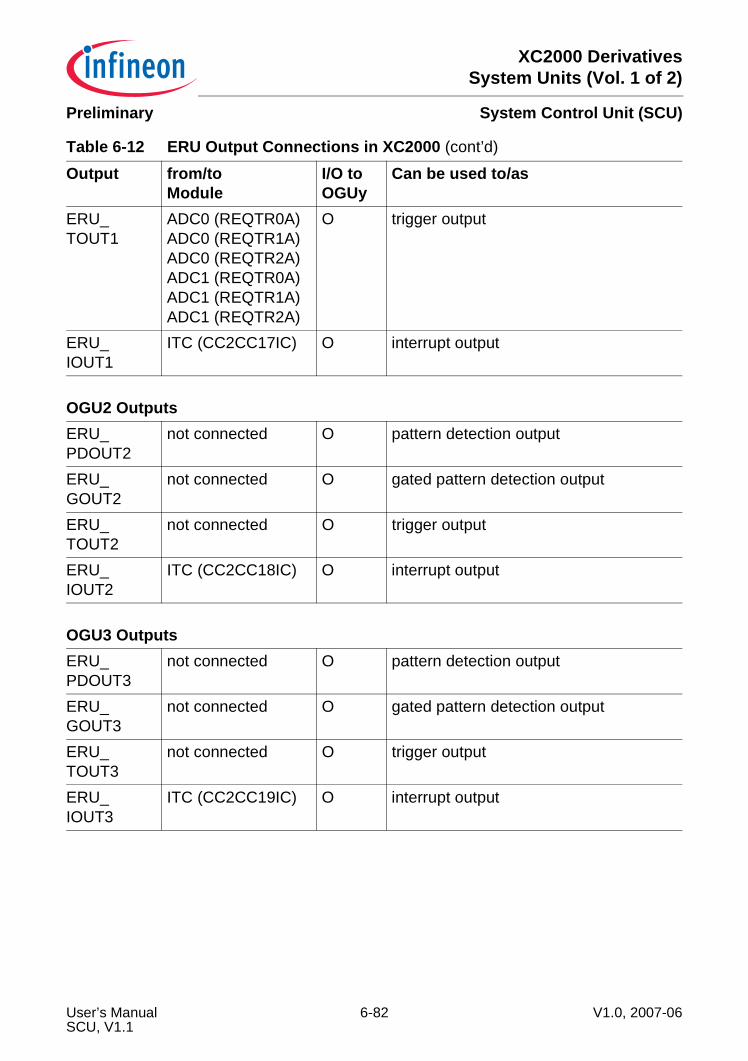
XC2000 DerivativesSystem Units (Vol. 1 of 2)
System Control Unit (SCU)Preliminary
ERU_TOUT1
ADC0 (REQTR0A)ADC0 (REQTR1A)ADC0 (REQTR2A)ADC1 (REQTR0A)ADC1 (REQTR1A)ADC1 (REQTR2A)
O trigger output
ERU_IOUT1
ITC (CC2CC17IC) O interrupt output
OGU2 OutputsERU_PDOUT2
not connected O pattern detection output
ERU_GOUT2
not connected O gated pattern detection output
ERU_TOUT2
not connected O trigger output
ERU_IOUT2
ITC (CC2CC18IC) O interrupt output
OGU3 OutputsERU_PDOUT3
not connected O pattern detection output
ERU_GOUT3
not connected O gated pattern detection output
ERU_TOUT3
not connected O trigger output
ERU_IOUT3
ITC (CC2CC19IC) O interrupt output
Table 6-12 ERU Output Connections in XC2000 (cont’d)
Output from/toModule
I/O to OGUy
Can be used to/as
User’s Manual 6-82 V1.0, 2007-06SCU, V1.1
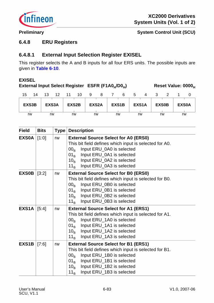
XC2000 DerivativesSystem Units (Vol. 1 of 2)
System Control Unit (SCU)Preliminary
6.4.8 ERU Registers
6.4.8.1 External Input Selection Register EXISELThis register selects the A and B inputs for all four ERS units. The possible inputs aregiven in Table 6-10.
EXISELExternal Input Select Register ESFR (F1A0H/D0H) Reset Value: 0000H
15 14 13 12 11 10 9 8 7 6 5 4 3 2 1 0
EXS3B EXS3A EXS2B EXS2A EXS1B EXS1A EXS0B EXS0A
rw rw rw rw rw rw rw rw
Field Bits Type DescriptionEXS0A [1:0] rw External Source Select for A0 (ERS0)
This bit field defines which input is selected for A0.00B Input ERU_0A0 is selected01B Input ERU_0A1 is selected10B Input ERU_0A2 is selected11B Input ERU_0A3 is selected
EXS0B [3:2] rw External Source Select for B0 (ERS0)This bit field defines which input is selected for B0.00B Input ERU_0B0 is selected01B Input ERU_0B1 is selected10B Input ERU_0B2 is selected11B Input ERU_0B3 is selected
EXS1A [5:4] rw External Source Select for A1 (ERS1)This bit field defines which input is selected for A1.00B Input ERU_1A0 is selected01B Input ERU_1A1 is selected10B Input ERU_1A2 is selected11B Input ERU_1A3 is selected
EXS1B [7:6] rw External Source Select for B1 (ERS1)This bit field defines which input is selected for B1.00B Input ERU_1B0 is selected01B Input ERU_1B1 is selected10B Input ERU_1B2 is selected11B Input ERU_1B3 is selected
User’s Manual 6-83 V1.0, 2007-06SCU, V1.1
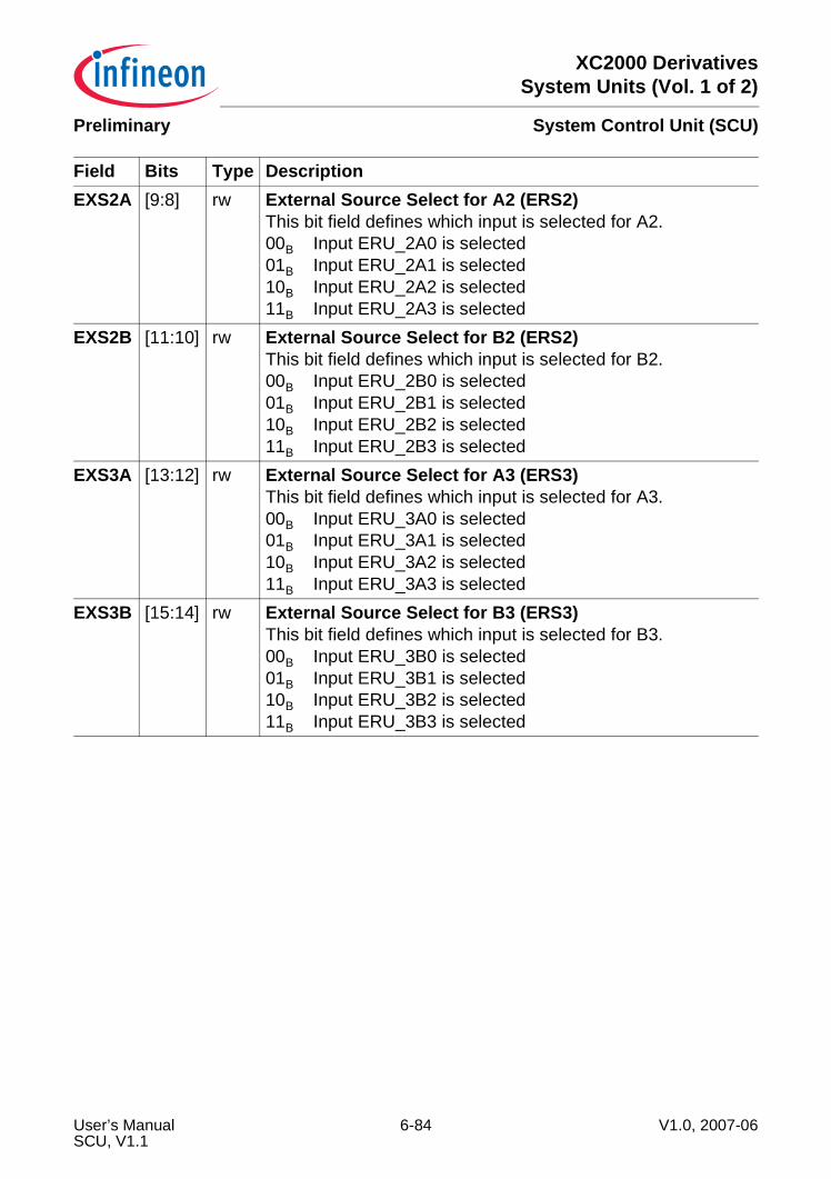
XC2000 DerivativesSystem Units (Vol. 1 of 2)
System Control Unit (SCU)Preliminary
EXS2A [9:8] rw External Source Select for A2 (ERS2)This bit field defines which input is selected for A2.00B Input ERU_2A0 is selected01B Input ERU_2A1 is selected10B Input ERU_2A2 is selected11B Input ERU_2A3 is selected
EXS2B [11:10] rw External Source Select for B2 (ERS2)This bit field defines which input is selected for B2.00B Input ERU_2B0 is selected01B Input ERU_2B1 is selected10B Input ERU_2B2 is selected11B Input ERU_2B3 is selected
EXS3A [13:12] rw External Source Select for A3 (ERS3)This bit field defines which input is selected for A3.00B Input ERU_3A0 is selected01B Input ERU_3A1 is selected10B Input ERU_3A2 is selected11B Input ERU_3A3 is selected
EXS3B [15:14] rw External Source Select for B3 (ERS3)This bit field defines which input is selected for B3.00B Input ERU_3B0 is selected01B Input ERU_3B1 is selected10B Input ERU_3B2 is selected11B Input ERU_3B3 is selected
Field Bits Type Description
User’s Manual 6-84 V1.0, 2007-06SCU, V1.1
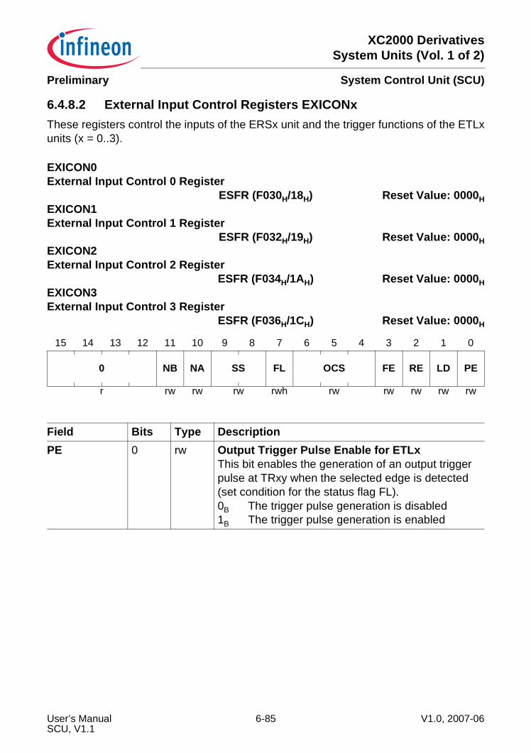
XC2000 DerivativesSystem Units (Vol. 1 of 2)
System Control Unit (SCU)Preliminary
6.4.8.2 External Input Control Registers EXICONxThese registers control the inputs of the ERSx unit and the trigger functions of the ETLxunits (x = 0..3).
EXICON0External Input Control 0 Register
ESFR (F030H/18H) Reset Value: 0000HEXICON1External Input Control 1 Register
ESFR (F032H/19H) Reset Value: 0000HEXICON2External Input Control 2 Register
ESFR (F034H/1AH) Reset Value: 0000HEXICON3External Input Control 3 Register
ESFR (F036H/1CH) Reset Value: 0000H
15 14 13 12 11 10 9 8 7 6 5 4 3 2 1 0
0 NB NA SS FL OCS FE RE LD PE
r rw rw rw rwh rw rw rw rw rw
Field Bits Type DescriptionPE 0 rw Output Trigger Pulse Enable for ETLx
This bit enables the generation of an output trigger pulse at TRxy when the selected edge is detected (set condition for the status flag FL).0B The trigger pulse generation is disabled1B The trigger pulse generation is enabled
User’s Manual 6-85 V1.0, 2007-06SCU, V1.1
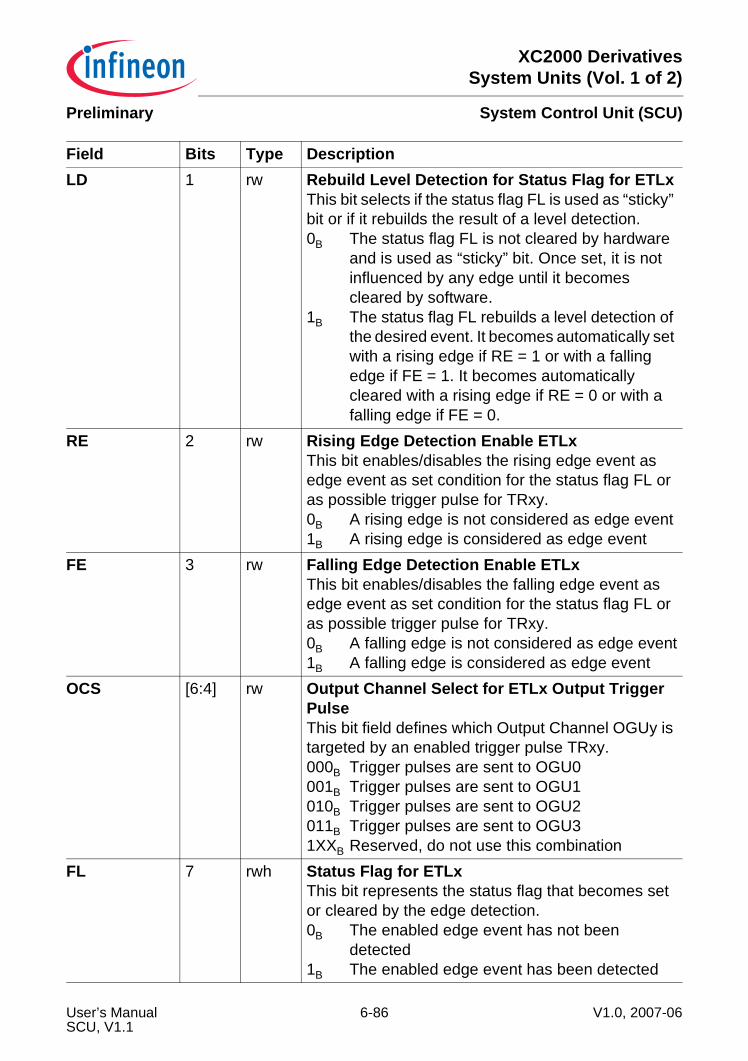
XC2000 DerivativesSystem Units (Vol. 1 of 2)
System Control Unit (SCU)Preliminary
LD 1 rw Rebuild Level Detection for Status Flag for ETLxThis bit selects if the status flag FL is used as “sticky” bit or if it rebuilds the result of a level detection.0B The status flag FL is not cleared by hardware
and is used as “sticky” bit. Once set, it is not influenced by any edge until it becomes cleared by software.
1B The status flag FL rebuilds a level detection of the desired event. It becomes automatically set with a rising edge if RE = 1 or with a falling edge if FE = 1. It becomes automatically cleared with a rising edge if RE = 0 or with a falling edge if FE = 0.
RE 2 rw Rising Edge Detection Enable ETLxThis bit enables/disables the rising edge event as edge event as set condition for the status flag FL or as possible trigger pulse for TRxy.0B A rising edge is not considered as edge event1B A rising edge is considered as edge event
FE 3 rw Falling Edge Detection Enable ETLxThis bit enables/disables the falling edge event as edge event as set condition for the status flag FL or as possible trigger pulse for TRxy.0B A falling edge is not considered as edge event1B A falling edge is considered as edge event
OCS [6:4] rw Output Channel Select for ETLx Output Trigger PulseThis bit field defines which Output Channel OGUy is targeted by an enabled trigger pulse TRxy.000B Trigger pulses are sent to OGU0001B Trigger pulses are sent to OGU1010B Trigger pulses are sent to OGU2011B Trigger pulses are sent to OGU31XXB Reserved, do not use this combination
FL 7 rwh Status Flag for ETLxThis bit represents the status flag that becomes set or cleared by the edge detection.0B The enabled edge event has not been
detected1B The enabled edge event has been detected
Field Bits Type Description
User’s Manual 6-86 V1.0, 2007-06SCU, V1.1
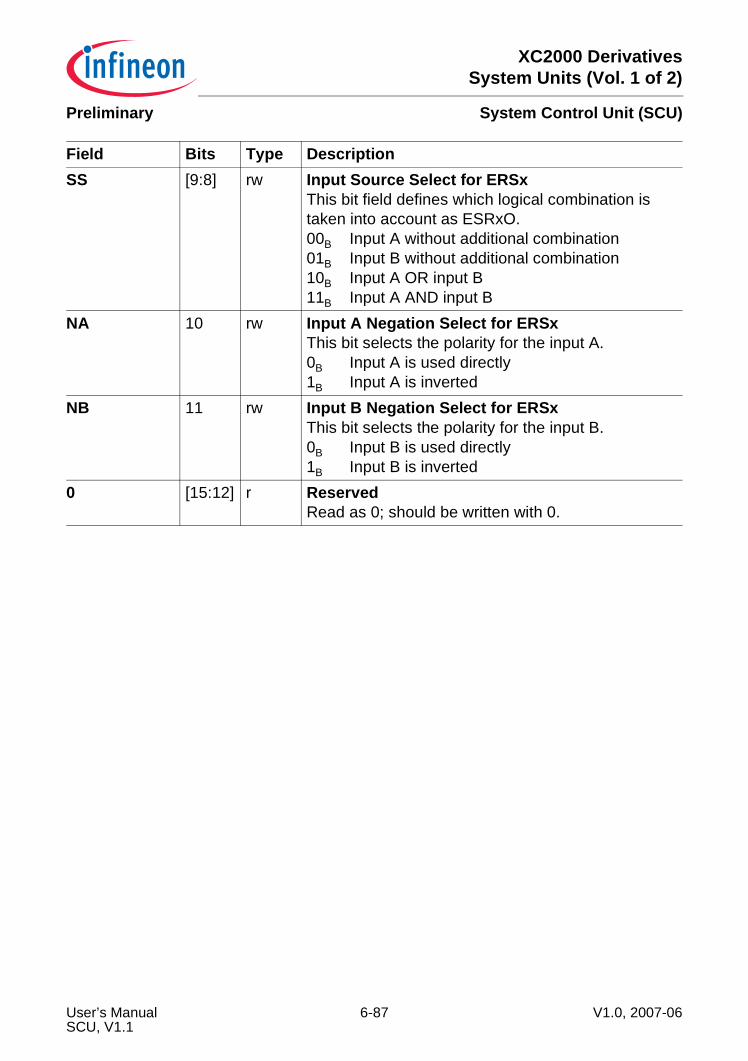
XC2000 DerivativesSystem Units (Vol. 1 of 2)
System Control Unit (SCU)Preliminary
SS [9:8] rw Input Source Select for ERSxThis bit field defines which logical combination is taken into account as ESRxO.00B Input A without additional combination01B Input B without additional combination10B Input A OR input B 11B Input A AND input B
NA 10 rw Input A Negation Select for ERSxThis bit selects the polarity for the input A.0B Input A is used directly1B Input A is inverted
NB 11 rw Input B Negation Select for ERSxThis bit selects the polarity for the input B.0B Input B is used directly1B Input B is inverted
0 [15:12] r ReservedRead as 0; should be written with 0.
Field Bits Type Description
User’s Manual 6-87 V1.0, 2007-06SCU, V1.1
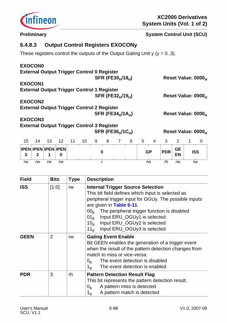
XC2000 DerivativesSystem Units (Vol. 1 of 2)
System Control Unit (SCU)Preliminary
6.4.8.3 Output Control Registers EXOCONyThese registers control the outputs of the Output Gating Unit y (y = 0..3).
EXOCON0External Output Trigger Control 0 Register
SFR (FE30H/18H) Reset Value: 0000HEXOCON1External Output Trigger Control 1 Register
SFR (FE32H/19H) Reset Value: 0000HEXOCON2External Output Trigger Control 2 Register
SFR (FE34H/1AH) Reset Value: 0000HEXOCON3External Output Trigger Control 3 Register
SFR (FE36H/1CH) Reset Value: 0000H
15 14 13 12 11 10 9 8 7 6 5 4 3 2 1 0
IPEN3
IPEN2
IPEN1
IPEN0 0 GP PDR GE
EN ISS
rw rw rw rw r rw rh rw rw
Field Bits Type DescriptionISS [1:0] rw Internal Trigger Source Selection
This bit field defines which input is selected as peripheral trigger input for OGUy. The possible inputs are given in Table 6-11.00B The peripheral trigger function is disabled01B Input ERU_OGUy1 is selected10B Input ERU_OGUy2 is selected11B Input ERU_OGUy3 is selected
GEEN 2 rw Gating Event EnableBit GEEN enables the generation of a trigger event when the result of the pattern detection changes from match to miss or vice-versa.0B The event detection is disabled1B The event detection is enabled
PDR 3 rh Pattern Detection Result FlagThis bit represents the pattern detection result.0B A pattern miss is detected1B A pattern match is detected
User’s Manual 6-88 V1.0, 2007-06SCU, V1.1
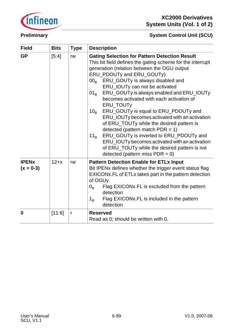
XC2000 DerivativesSystem Units (Vol. 1 of 2)
System Control Unit (SCU)Preliminary
GP [5:4] rw Gating Selection for Pattern Detection ResultThis bit field defines the gating scheme for the interrupt generation (relation between the OGU output ERU_PDOUTy and ERU_GOUTy).00B ERU_GOUTy is always disabled and
ERU_IOUTy can not be activated01B ERU_GOUTy is always enabled and ERU_IOUTy
becomes activated with each activation of ERU_TOUTy
10B ERU_GOUTy is equal to ERU_PDOUTy and ERU_IOUTy becomes activated with an activation of ERU_TOUTy while the desired pattern is detected (pattern match PDR = 1)
11B ERU_GOUTy is inverted to ERU_PDOUTy and ERU_IOUTy becomes activated with an activation of ERU_TOUTy while the desired pattern is not detected (pattern miss PDR = 0)
IPENx(x = 0-3)
12+x rw Pattern Detection Enable for ETLx InputBit IPENx defines whether the trigger event status flag EXICONx.FL of ETLx takes part in the pattern detection of OGUy.0B Flag EXICONx.FL is excluded from the pattern
detection1B Flag EXICONx.FL is included in the pattern
detection0 [11:6] r Reserved
Read as 0; should be written with 0.
Field Bits Type Description
User’s Manual 6-89 V1.0, 2007-06SCU, V1.1
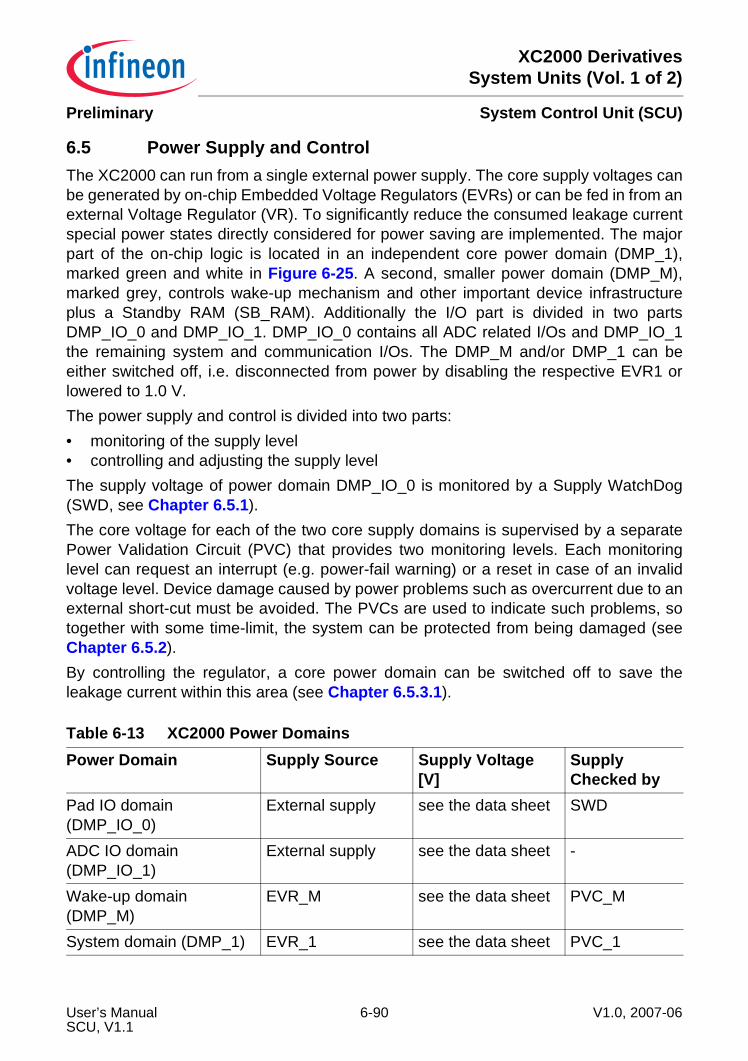
XC2000 DerivativesSystem Units (Vol. 1 of 2)
System Control Unit (SCU)Preliminary
6.5 Power Supply and ControlThe XC2000 can run from a single external power supply. The core supply voltages canbe generated by on-chip Embedded Voltage Regulators (EVRs) or can be fed in from anexternal Voltage Regulator (VR). To significantly reduce the consumed leakage currentspecial power states directly considered for power saving are implemented. The majorpart of the on-chip logic is located in an independent core power domain (DMP_1),marked green and white in Figure 6-25. A second, smaller power domain (DMP_M),marked grey, controls wake-up mechanism and other important device infrastructureplus a Standby RAM (SB_RAM). Additionally the I/O part is divided in two partsDMP_IO_0 and DMP_IO_1. DMP_IO_0 contains all ADC related I/Os and DMP_IO_1the remaining system and communication I/Os. The DMP_M and/or DMP_1 can beeither switched off, i.e. disconnected from power by disabling the respective EVR1 orlowered to 1.0 V.The power supply and control is divided into two parts:• monitoring of the supply level• controlling and adjusting the supply levelThe supply voltage of power domain DMP_IO_0 is monitored by a Supply WatchDog(SWD, see Chapter 6.5.1).The core voltage for each of the two core supply domains is supervised by a separatePower Validation Circuit (PVC) that provides two monitoring levels. Each monitoringlevel can request an interrupt (e.g. power-fail warning) or a reset in case of an invalidvoltage level. Device damage caused by power problems such as overcurrent due to anexternal short-cut must be avoided. The PVCs are used to indicate such problems, sotogether with some time-limit, the system can be protected from being damaged (seeChapter 6.5.2).By controlling the regulator, a core power domain can be switched off to save theleakage current within this area (see Chapter 6.5.3.1).
Table 6-13 XC2000 Power DomainsPower Domain Supply Source Supply Voltage
[V]Supply Checked by
Pad IO domain (DMP_IO_0)
External supply see the data sheet SWD
ADC IO domain (DMP_IO_1)
External supply see the data sheet -
Wake-up domain (DMP_M)
EVR_M see the data sheet PVC_M
System domain (DMP_1) EVR_1 see the data sheet PVC_1
User’s Manual 6-90 V1.0, 2007-06SCU, V1.1
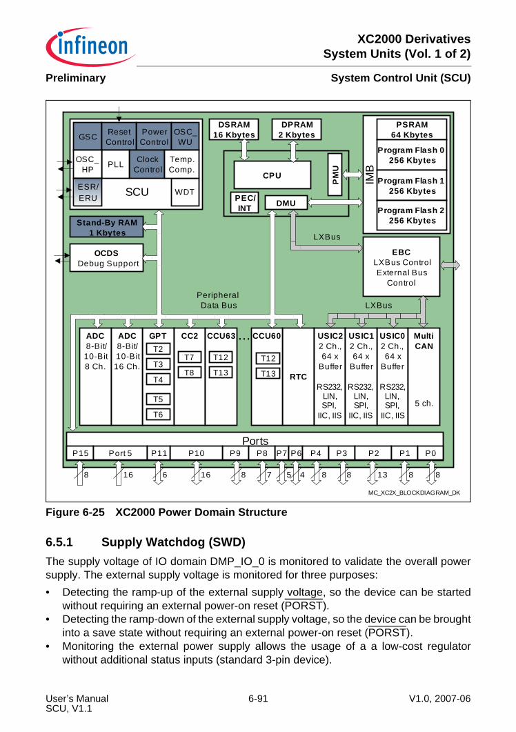
XC2000 DerivativesSystem Units (Vol. 1 of 2)
System Control Unit (SCU)Preliminary
Figure 6-25 XC2000 Power Domain Structure
6.5.1 Supply Watchdog (SWD)The supply voltage of IO domain DMP_IO_0 is monitored to validate the overall powersupply. The external supply voltage is monitored for three purposes:• Detecting the ramp-up of the external supply voltage, so the device can be started
without requiring an external power-on reset (PORST).• Detecting the ramp-down of the external supply voltage, so the device can be brought
into a save state without requiring an external power-on reset (PORST).• Monitoring the external power supply allows the usage of a a low-cost regulator
without additional status inputs (standard 3-pin device).
DPRAM2 Kbytes
CPU
PM
U
DMU
BRGen
ADC8-Bit/10-Bit8 Ch.
USIC02 Ch.,64 x
Buffer
RS232,LIN,SPI,
IIC, IIS
RTC
EBCLXBus ControlExternal Bus
Control
DSRAM16 Kbytes
PSRAM64 Kbytes
OCDSDebug Support
PeripheralData Bus
8
P15 P9 P7 P6Port 5 P4 P3 P2 P1 P0
888 1384516 8
MC_XC2X_BLOCKDIAGRAM_DK
Program Flash 0256 Kbytes
Program Flash 1256 Kbytes
Program Flash 2256 Kbytes
GPT
T6
T5
T4
T3
T2ADC8-Bit/10-Bit16 Ch.
CC2
T8
T7
MultiCAN
5 ch.
USIC22 Ch.,64 x
Buffer
RS232,LIN,SPI,
IIC, IIS
USIC12 Ch.,64 x
Buffer
RS232,LIN,SPI,
IIC, IIS
CCU63
T13
T12
CCU60
T13
T12
LXBus
P8
7
P10
16
P11
6
...
PowerControlGSC Reset
Control
ClockControlPLL
OSC_WU
OSC_HP
ESR/ERU
WDT
Temp.Comp.
SCU
IMB
Stand-By RAM1 Kbytes
PEC/INT
LXBus
Ports
User’s Manual 6-91 V1.0, 2007-06SCU, V1.1
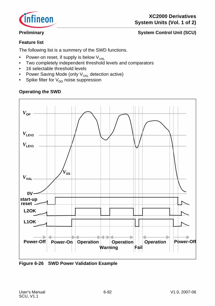
XC2000 DerivativesSystem Units (Vol. 1 of 2)
System Control Unit (SCU)Preliminary
Feature listThe following list is a summery of the SWD functions.• Power-on reset, if supply is below VVAL• Two completely independent threshold levels and comparators• 16 selectable threshold levels• Power Saving Mode (only VVAL detection active)• Spike filter for VDD noise suppression
Operating the SWD
Figure 6-26 SWD Power Validation Example
VOP
VLEV2
VLEV1
VVAL
L2OK
L1OK
Power-Off Power-On Power-OffOperation Operation OperationWarning Fail
VSS
0Vstart-upreset
User’s Manual 6-92 V1.0, 2007-06SCU, V1.1
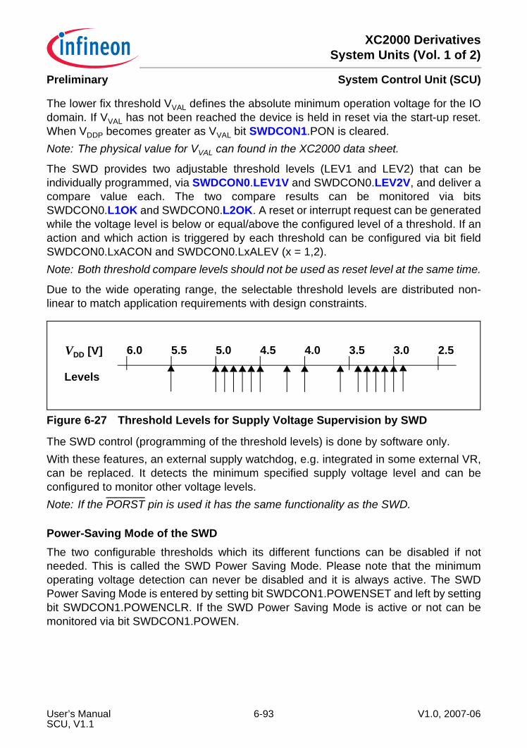
XC2000 DerivativesSystem Units (Vol. 1 of 2)
System Control Unit (SCU)Preliminary
The lower fix threshold VVAL defines the absolute minimum operation voltage for the IOdomain. If VVAL has not been reached the device is held in reset via the start-up reset.When VDDP becomes greater as VVAL bit SWDCON1.PON is cleared.Note: The physical value for VVAL can found in the XC2000 data sheet.
The SWD provides two adjustable threshold levels (LEV1 and LEV2) that can beindividually programmed, via SWDCON0.LEV1V and SWDCON0.LEV2V, and deliver acompare value each. The two compare results can be monitored via bitsSWDCON0.L1OK and SWDCON0.L2OK. A reset or interrupt request can be generatedwhile the voltage level is below or equal/above the configured level of a threshold. If anaction and which action is triggered by each threshold can be configured via bit fieldSWDCON0.LxACON and SWDCON0.LxALEV (x = 1,2).Note: Both threshold compare levels should not be used as reset level at the same time.
Due to the wide operating range, the selectable threshold levels are distributed non-linear to match application requirements with design constraints.
Figure 6-27 Threshold Levels for Supply Voltage Supervision by SWD
The SWD control (programming of the threshold levels) is done by software only.With these features, an external supply watchdog, e.g. integrated in some external VR,can be replaced. It detects the minimum specified supply voltage level and can beconfigured to monitor other voltage levels.Note: If the PORST pin is used it has the same functionality as the SWD.
Power-Saving Mode of the SWDThe two configurable thresholds which its different functions can be disabled if notneeded. This is called the SWD Power Saving Mode. Please note that the minimumoperating voltage detection can never be disabled and it is always active. The SWDPower Saving Mode is entered by setting bit SWDCON1.POWENSET and left by settingbit SWDCON1.POWENCLR. If the SWD Power Saving Mode is active or not can bemonitored via bit SWDCON1.POWEN.
Levels
VDD [V] 5.5 5.0 4.5 4.0 3.5 3.0 2.56.0
User’s Manual 6-93 V1.0, 2007-06SCU, V1.1
XC2000 DerivativesSystem Units (Vol. 1 of 2)
System Control Unit (SCU)Preliminary
6.5.1.1 SWD Control RegistersThe following registers are the software interface for the SWD.
SWDCON0SWD Control 0 Register ESFR (F080H/40H) Reset Value: 0941H
15 14 13 12 11 10 9 8 7 6 5 4 3 2 1 0
L2ALEV L2ACON L2
OK LEV2V L1ALEV L1ACON L1
OK LEV1V
rw rw rh rw rw rw rh rw
Field Bits Type DescriptionLEV1V [3:0] rw Level Threshold 1 Voltage
This bit field defines the voltage level that is used as threshold 1 check level.The values of the level thresholds are listed in the data sheet.
L1OK 4 rh Level Threshold 1 Check Ok Status0B The supply voltage is below level threshold 11B The supply voltage is equal or higher than level
threshold 1L1ACON [6:5] rw Level Threshold 1 Action Control
This bit field defines which action is requested if the condition is violated (voltage is below the defined level threshold 1).00B No action is requested01B An interrupt is requested10B A reset request is generated11B A reset and interrupt request is generated
L1ALEV 7 rw Level threshold 1 Action Level0B The action configured by bit field L1ACON is
requested when the voltage is below LEV1V. Otherwise no action is requested.
1B The action configured by bit field L1ACON is requested when the voltage is equal or above LEV1V. Otherwise no action is requested.
User’s Manual 6-94 V1.0, 2007-06SCU, V1.1
XC2000 DerivativesSystem Units (Vol. 1 of 2)
System Control Unit (SCU)Preliminary
LEV2V [11:8] rw Level Threshold 2 VoltageThis bit field defines the voltage level that is used as check level threshold 2.The values of the level thresholds are listed in the data sheet.
L2OK 12 rh Level Threshold 2 Check Ok Status0B The supply voltage is below the selected level
threshold 21B The supply voltage is equal or higher than the
selected level threshold 2L2ACON [14:13] rw Level Threshold 2 Action Control
This bit field defines for which action is requested if the condition is violated (voltage is below the defined level threshold 2).00B No action is requested01B An interrupt is requested10B A reset request is generated11B A reset and interrupt request is generated
L2ALEV 15 rw Level Threshold 2 Action Level0B The action configured by bit field L2ACON is
requested when the voltage is below LEV2V. Otherwise no action is requested.
1B The action configured by bit field L2ACON is requested when the voltage is equal or above LEV2V. Otherwise no action is requested.
SWDCON1SWD Control 1 Register ESFR (F082H/41H) Reset Value: 0000H
15 14 13 12 11 10 9 8 7 6 5 4 3 2 1 0
0 CLRPON PON POW
EN
POWEN
SET
POWEN
CLRr w rh rh w w
Field Bits Type Description
User’s Manual 6-95 V1.0, 2007-06SCU, V1.1
XC2000 DerivativesSystem Units (Vol. 1 of 2)
System Control Unit (SCU)Preliminary
Field Bits Type DescriptionPOWENCLR 0 w SWD Power Saving Mode Enable Clear
0B Clearing this bit has no effect1B Setting this bit clears bit POWENReading this bit returns always zero.
POWENSET 1 w SWD Power Saving Mode Enable Set0B Clearing this bit has no effect1B Setting this bit set bit POWENReading this bit returns always zero.
POWEN 2 rh SWD Power Saving Mode Enable0B The SWD Power Saving Mode is disabled1B The SWD Power Saving Mode is enabled
PON 3 rh Power-On Status Flag0B No power-on event occurred1B A power-on event occurred
CLRPON 4 w Clear Power-On Status Flag0B Bit PON is not changed1B Bit PON is cleared
0 [15:5] r ReservedRead as 0; should be written with 0.
User’s Manual 6-96 V1.0, 2007-06SCU, V1.1
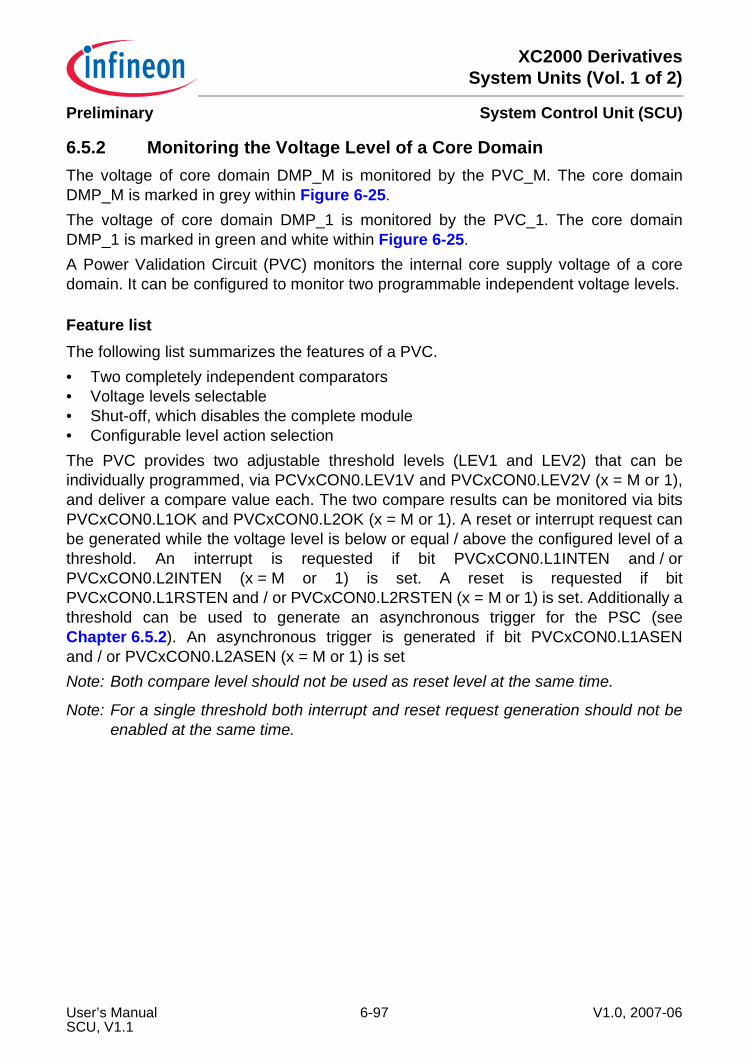
XC2000 DerivativesSystem Units (Vol. 1 of 2)
System Control Unit (SCU)Preliminary
6.5.2 Monitoring the Voltage Level of a Core DomainThe voltage of core domain DMP_M is monitored by the PVC_M. The core domainDMP_M is marked in grey within Figure 6-25.The voltage of core domain DMP_1 is monitored by the PVC_1. The core domainDMP_1 is marked in green and white within Figure 6-25.A Power Validation Circuit (PVC) monitors the internal core supply voltage of a coredomain. It can be configured to monitor two programmable independent voltage levels.
Feature listThe following list summarizes the features of a PVC.• Two completely independent comparators• Voltage levels selectable• Shut-off, which disables the complete module• Configurable level action selectionThe PVC provides two adjustable threshold levels (LEV1 and LEV2) that can beindividually programmed, via PCVxCON0.LEV1V and PVCxCON0.LEV2V (x = M or 1),and deliver a compare value each. The two compare results can be monitored via bitsPVCxCON0.L1OK and PVCxCON0.L2OK (x = M or 1). A reset or interrupt request canbe generated while the voltage level is below or equal / above the configured level of athreshold. An interrupt is requested if bit PVCxCON0.L1INTEN and / orPVCxCON0.L2INTEN (x = M or 1) is set. A reset is requested if bitPVCxCON0.L1RSTEN and / or PVCxCON0.L2RSTEN (x = M or 1) is set. Additionally athreshold can be used to generate an asynchronous trigger for the PSC (seeChapter 6.5.2). An asynchronous trigger is generated if bit PVCxCON0.L1ASENand / or PVCxCON0.L2ASEN (x = M or 1) is setNote: Both compare level should not be used as reset level at the same time.
Note: For a single threshold both interrupt and reset request generation should not beenabled at the same time.
User’s Manual 6-97 V1.0, 2007-06SCU, V1.1
XC2000 DerivativesSystem Units (Vol. 1 of 2)
System Control Unit (SCU)Preliminary
6.5.2.1 PVC Status and Control RegistersThese registers are the software interface for the PVCs.
PVCMCON0PVC_M Control Step 0 Register
ESFR (F1E4H) Reset Value: 0544H
15 14 13 12 11 10 9 8 7 6 5 4 3 2 1 0
L2ASEN
L2RSTE
N
L2INTEN
L2ALEV
LEV2OK LEV2V L1A
SEN
L1RSTE
N
L1INTEN
L1ALEV
LEV1OK LEV1V
rwh rwh rwh rwh rh rwh rwh rwh rwh rwh rh rwh
Field Bits Type DescriptionLEV1V [2:0] rwh Level Threshold 1 Voltage Configuration
This bit field defines the level of threshold 1 that is compared with the DMP_M core voltage.The values for the different configurations are listed in the data sheet.
LEV1OK 3 rh Level Threshold 1 Check Result0B The core voltage of the DMP_M is below the
configured level of threshold 11B The core voltage of the DMP_M is equal or
above the configured level of threshold 1L1ALEV 4 rwh Level Threshold 1 Action Level
0B The action configured by bits L1INTEN, L1RSTEN, and L1ASEN are requested when the core voltage is below LEV1V. Otherwise no action is requested.
1B The actions configured by bits L1INTEN, L1RSTEN, and L1ASEN are requested when the core voltage is equal or above LEV1V. Otherwise no action is requested.
L1INTEN 5 rwh Level Threshold 1 Interrupt Request EnableThis bit defines if an interrupt request trigger is requested if the comparison check was successful. When a check is successful is defined via bit L1ALEV.0B No interrupt is requested1B An interrupt is requested
User’s Manual 6-98 V1.0, 2007-06SCU, V1.1
XC2000 DerivativesSystem Units (Vol. 1 of 2)
System Control Unit (SCU)Preliminary
L1RSTEN 6 rwh Level Threshold 1 Reset Request EnableThis bit defines if a reset request trigger is requested if the comparison check was successful. When a check is successful is defined via bit L1ALEV.0B No reset is requested1B An reset is requested
L1ASEN 7 rwh Level Threshold 1 Asynchronous Action EnableThis bit defines if asynchronous action can be performed if the comparison check was successful. When a check is successful is defined via bit L1ALEV.0B No asynchronous actions are performed1B Asynchronous actions can be performed
LEV2V [10:8] rwh Level Threshold 2 Voltage ConfigurationThis bit field defines the level of threshold 2 that is compared with the DMP_M core voltage.The values for the different configurations are listed in the data sheet.
LEV2OK 11 rh Level Threshold 2 Check Result0B The core voltage of the DMP_M is below the
configured level of threshold 21B The core voltage of the DMP_M is equal or
above the configured level of threshold 2L2ALEV 12 rwh Level Threshold 2 Action Level
0B The action configured by bits L2INTEN, L2RSTEN, and L2ASEN are requested when the core voltage is below LEV2V. Otherwise no action is requested.
1B The action configured by bits L2INTEN, L2RSTEN, and L2ASEN are requested when the core voltage is equal or above LEV2V. Otherwise no action is requested.
L2INTEN 13 rwh Level Threshold 2 Interrupt Request EnableThis bit defines if an interrupt request trigger is requested if the comparison check was successful. When a check is successful is defined via bit L2ALEV.0B No interrupt is requested1B An interrupt is requested
Field Bits Type Description
User’s Manual 6-99 V1.0, 2007-06SCU, V1.1

XC2000 DerivativesSystem Units (Vol. 1 of 2)
System Control Unit (SCU)Preliminary
L2RSTEN 14 rwh Level Threshold 2 Reset Request EnableThis bit defines if a reset request trigger is requested if the comparison check was successful. When a check is successful is defined via bit L2ALEV.0B No reset is requested1B An reset is requested
L2ASEN 15 rwh Level Threshold 2 Asynchronous Action EnableThis bit defines if asynchronous action can be performed if the comparison check was successful. When a check is successful is defined via bit L2ALEV.0B No asynchronous actions are performed1B Asynchronous actions can be performed
PVC1CON0PVC_1 Control Step 0 Register
ESFR (F014H/0AH) Reset Value: 0504H
15 14 13 12 11 10 9 8 7 6 5 4 3 2 1 0
L2ASEN
L2RSTE
N
L2INTEN
L2ALEV
LEV2OK LEV2V L1A
SEN
L1RSTE
N
L1INTEN
L1ALEV
LEV1OK LEV1V
rwh rwh rwh rwh rh rwh rwh rwh rwh rwh rh rwh
Field Bits Type DescriptionLEV1V [2:0] rwh Level Threshold 1 Voltage Configuration
This bit field defines the level of threshold 1 that is compared with the DMP_1 core voltage. The values for the different configurations are listed in the data sheet.
LEV1OK 3 rh Level Threshold 1 Check Result0B The core voltage of the DMP_1 is below the
configured threshold level 11B The core voltage of the DMP_1 is equal or
above the configured threshold level 1
Field Bits Type Description
User’s Manual 6-100 V1.0, 2007-06SCU, V1.1
XC2000 DerivativesSystem Units (Vol. 1 of 2)
System Control Unit (SCU)Preliminary
L1ALEV 4 rwh Level Threshold 1 Action Level0B The action configured by bits L1INTEN,
L1RSTEN, and L1ASEN are requested when the core voltage is below LEV1V. Otherwise no action is requested.
1B The actions configured by bits L1INTEN, L1RSTEN, and L1ASEN are requested when the core voltage is equal or above LEV1V. Otherwise no action is requested.
L1INTEN 5 rwh Level Threshold 1 Interrupt Request EnableThis bit defines if an interrupt request trigger is requested if the comparison check was successful. When a check is successful is defined via bit L1ALEV.0B No interrupt is requested1B An interrupt is requested
L1RSTEN 6 rwh Level Threshold 1 Reset Request EnableThis bit defines if a reset request trigger is requested if the comparison check was successful. When a check is successful is defined via bit L1ALEV.0B No reset is requested1B An reset is requested
L1ASEN 7 rwh Level Threshold 1 Asynchronous Action EnableThis bit defines if asynchronous action can be performed if the comparison check was successful. When a check is successful is defined via bit L1ALEV.0B No asynchronous actions are performed1B Asynchronous actions can be performed
LEV2V [10:8] rwh Level Threshold 2 Voltage ConfigurationThis bit field defines the level of threshold 2 that is compared with the DMP_1 core voltage.The values for the different configurations are listed in the data sheet.
LEV2OK 11 rh Level Threshold 2 Check Result0B The core supply voltage of the DMP_1 is below
the configured threshold level 21B The core supply voltage of the DMP_1 is equal
or above the configured threshold level 2
Field Bits Type Description
User’s Manual 6-101 V1.0, 2007-06SCU, V1.1

XC2000 DerivativesSystem Units (Vol. 1 of 2)
System Control Unit (SCU)Preliminary
L2ALEV 12 rwh Level Threshold 2 Action Level0B The action configured by bits L2INTEN,
L2RSTEN, and L2ASEN are requested when the voltage is below LEV2V. Otherwise no action is requested.
1B The action configured by bits L2INTEN, L2RSTEN, and L2ASEN are requested when the voltage is equal or above LEV2V. Otherwise no action is requested.
L2INTEN 13 rwh Level Threshold 2 Interrupt Request EnableThis bit defines if an interrupt request trigger is requested if the comparison check was successful. When a check is successful is defined via bit L2ALEV.0B No interrupt is requested1B An interrupt is requested
L2RSTEN 14 rwh Level Threshold 2 Reset Request EnableThis bit defines if a reset request trigger is requested if the comparison check was successful. When a check is successful is defined via bit L2ALEV.0B No reset is requested1B An reset is requested
L2ASEN 15 rwh Level Threshold 2 Asynchronous Action EnableThis bit defines if asynchronous action can be performed if the comparison check was successful. When a check is successful is defined via bit L2ALEV.0B No asynchronous actions are performed1B Asynchronous actions can be performed
Field Bits Type Description
User’s Manual 6-102 V1.0, 2007-06SCU, V1.1
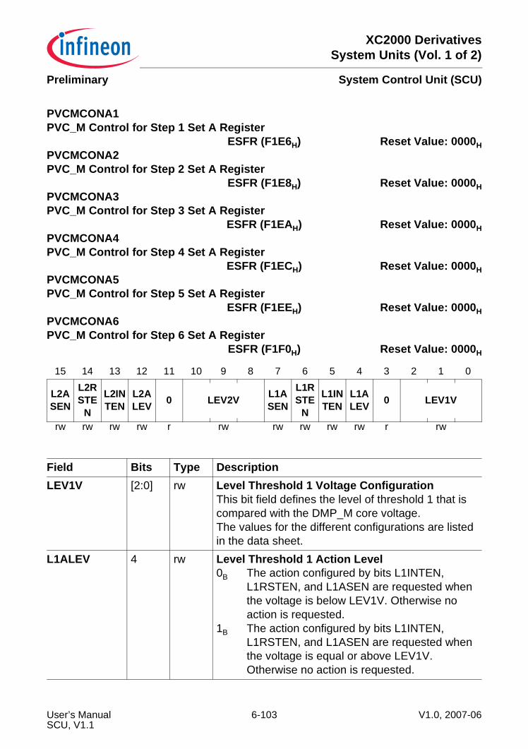
XC2000 DerivativesSystem Units (Vol. 1 of 2)
System Control Unit (SCU)Preliminary
PVCMCONA1PVC_M Control for Step 1 Set A Register
ESFR (F1E6H) Reset Value: 0000HPVCMCONA2PVC_M Control for Step 2 Set A Register
ESFR (F1E8H) Reset Value: 0000HPVCMCONA3PVC_M Control for Step 3 Set A Register
ESFR (F1EAH) Reset Value: 0000HPVCMCONA4PVC_M Control for Step 4 Set A Register
ESFR (F1ECH) Reset Value: 0000HPVCMCONA5PVC_M Control for Step 5 Set A Register
ESFR (F1EEH) Reset Value: 0000HPVCMCONA6PVC_M Control for Step 6 Set A Register
ESFR (F1F0H) Reset Value: 0000H
15 14 13 12 11 10 9 8 7 6 5 4 3 2 1 0
L2ASEN
L2RSTE
N
L2INTEN
L2ALEV 0 LEV2V L1A
SEN
L1RSTE
N
L1INTEN
L1ALEV 0 LEV1V
rw rw rw rw r rw rw rw rw rw r rw
Field Bits Type DescriptionLEV1V [2:0] rw Level Threshold 1 Voltage Configuration
This bit field defines the level of threshold 1 that is compared with the DMP_M core voltage.The values for the different configurations are listed in the data sheet.
L1ALEV 4 rw Level Threshold 1 Action Level0B The action configured by bits L1INTEN,
L1RSTEN, and L1ASEN are requested when the voltage is below LEV1V. Otherwise no action is requested.
1B The action configured by bits L1INTEN, L1RSTEN, and L1ASEN are requested when the voltage is equal or above LEV1V. Otherwise no action is requested.
User’s Manual 6-103 V1.0, 2007-06SCU, V1.1

XC2000 DerivativesSystem Units (Vol. 1 of 2)
System Control Unit (SCU)Preliminary
L1INTEN 5 rw Level Threshold 1 Interrupt Request EnableThis bit defines if an interrupt request trigger is requested if the comparison check was successful. When a check is successful is defined via bit L1ALEV.0B No interrupt is requested1B An interrupt is requested
L1RSTEN 6 rw Level Threshold 1 Reset Request EnableThis bit defines if a reset request trigger is requested if the comparison check was successful. When a check is successful is defined via bit L1ALEV.0B No reset is requested1B An reset is requested
L1ASEN 7 rw Level Threshold 1 Asynchronous Action EnableThis bit defines if asynchronous action can be performed if the comparison check was successful. When a check is successful is defined via bit L1ALEV.0B No asynchronous actions are performed1B Asynchronous actions can be performed
LEV2V [10:8] rw Level Threshold 2 Voltage ConfigurationThis bit field defines the level of threshold 2 that is compared with the DMP_M core voltage.The values for the different configurations are listed in the data sheet.
L2ALEV 12 rw Level Threshold 2 Action Level0B The action configured by bits L2INTEN,
L2RSTEN, and L2ASEN are requested when the voltage is below LEV2V. Otherwise no action is requested.
1B The action configured by bits L2INTEN, L2RSTEN, and L2ASEN are requested when the voltage is equal or above LEV2V. Otherwise no action is requested.
Field Bits Type Description
User’s Manual 6-104 V1.0, 2007-06SCU, V1.1
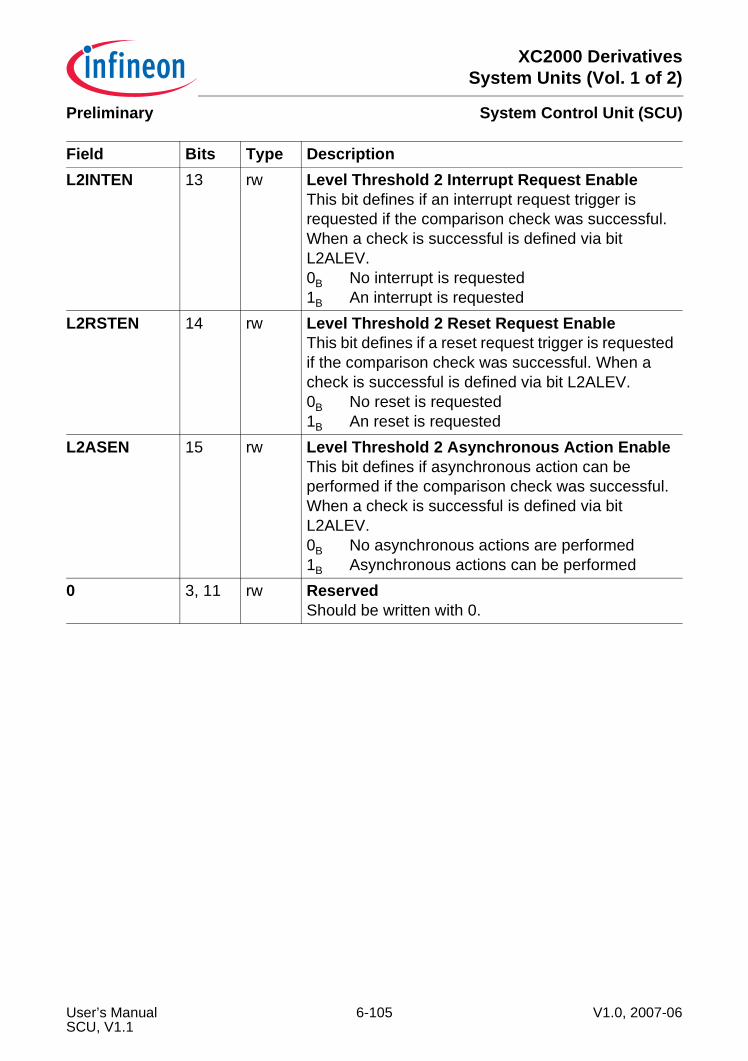
XC2000 DerivativesSystem Units (Vol. 1 of 2)
System Control Unit (SCU)Preliminary
L2INTEN 13 rw Level Threshold 2 Interrupt Request EnableThis bit defines if an interrupt request trigger is requested if the comparison check was successful. When a check is successful is defined via bit L2ALEV.0B No interrupt is requested1B An interrupt is requested
L2RSTEN 14 rw Level Threshold 2 Reset Request EnableThis bit defines if a reset request trigger is requested if the comparison check was successful. When a check is successful is defined via bit L2ALEV.0B No reset is requested1B An reset is requested
L2ASEN 15 rw Level Threshold 2 Asynchronous Action EnableThis bit defines if asynchronous action can be performed if the comparison check was successful. When a check is successful is defined via bit L2ALEV.0B No asynchronous actions are performed1B Asynchronous actions can be performed
0 3, 11 rw ReservedShould be written with 0.
Field Bits Type Description
User’s Manual 6-105 V1.0, 2007-06SCU, V1.1
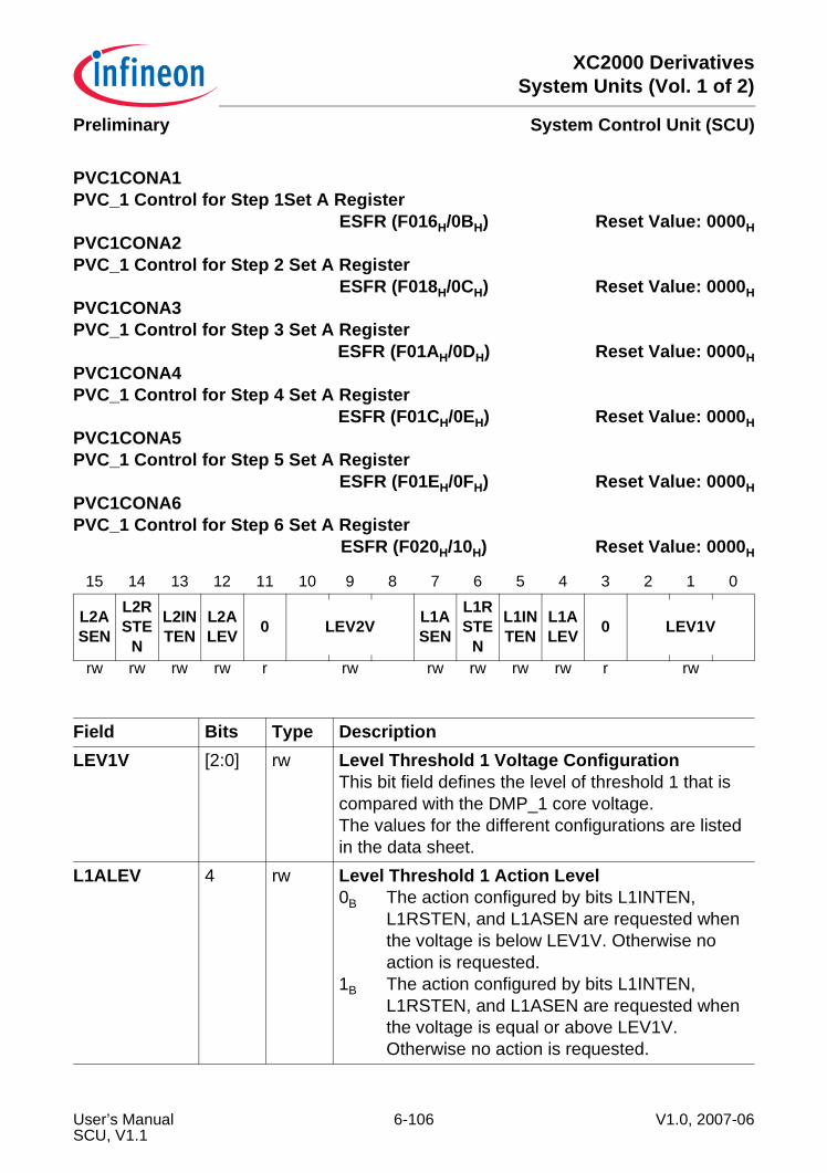
XC2000 DerivativesSystem Units (Vol. 1 of 2)
System Control Unit (SCU)Preliminary
PVC1CONA1PVC_1 Control for Step 1Set A Register
ESFR (F016H/0BH) Reset Value: 0000HPVC1CONA2PVC_1 Control for Step 2 Set A Register
ESFR (F018H/0CH) Reset Value: 0000HPVC1CONA3PVC_1 Control for Step 3 Set A Register
ESFR (F01AH/0DH) Reset Value: 0000HPVC1CONA4PVC_1 Control for Step 4 Set A Register
ESFR (F01CH/0EH) Reset Value: 0000HPVC1CONA5PVC_1 Control for Step 5 Set A Register
ESFR (F01EH/0FH) Reset Value: 0000HPVC1CONA6PVC_1 Control for Step 6 Set A Register
ESFR (F020H/10H) Reset Value: 0000H
15 14 13 12 11 10 9 8 7 6 5 4 3 2 1 0
L2ASEN
L2RSTE
N
L2INTEN
L2ALEV 0 LEV2V L1A
SEN
L1RSTE
N
L1INTEN
L1ALEV 0 LEV1V
rw rw rw rw r rw rw rw rw rw r rw
Field Bits Type DescriptionLEV1V [2:0] rw Level Threshold 1 Voltage Configuration
This bit field defines the level of threshold 1 that is compared with the DMP_1 core voltage.The values for the different configurations are listed in the data sheet.
L1ALEV 4 rw Level Threshold 1 Action Level0B The action configured by bits L1INTEN,
L1RSTEN, and L1ASEN are requested when the voltage is below LEV1V. Otherwise no action is requested.
1B The action configured by bits L1INTEN, L1RSTEN, and L1ASEN are requested when the voltage is equal or above LEV1V. Otherwise no action is requested.
User’s Manual 6-106 V1.0, 2007-06SCU, V1.1
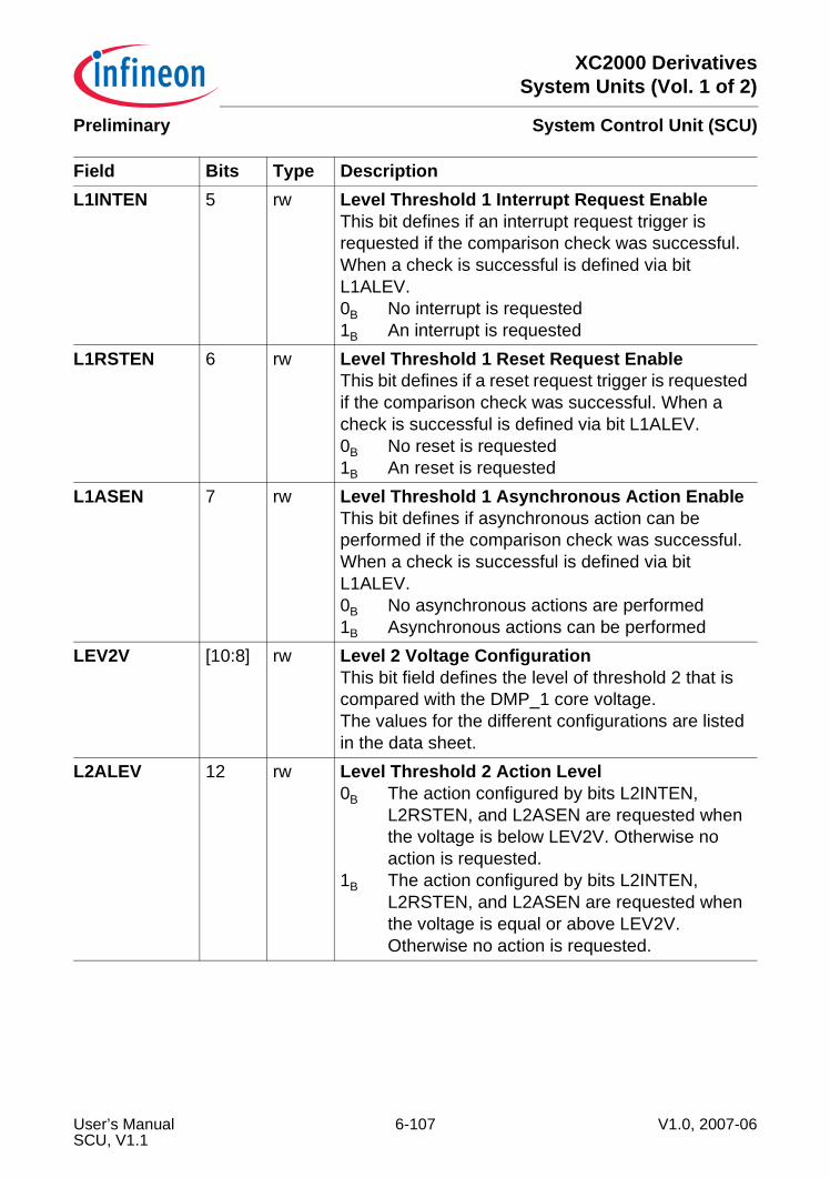
XC2000 DerivativesSystem Units (Vol. 1 of 2)
System Control Unit (SCU)Preliminary
L1INTEN 5 rw Level Threshold 1 Interrupt Request EnableThis bit defines if an interrupt request trigger is requested if the comparison check was successful. When a check is successful is defined via bit L1ALEV.0B No interrupt is requested1B An interrupt is requested
L1RSTEN 6 rw Level Threshold 1 Reset Request EnableThis bit defines if a reset request trigger is requested if the comparison check was successful. When a check is successful is defined via bit L1ALEV.0B No reset is requested1B An reset is requested
L1ASEN 7 rw Level Threshold 1 Asynchronous Action EnableThis bit defines if asynchronous action can be performed if the comparison check was successful. When a check is successful is defined via bit L1ALEV.0B No asynchronous actions are performed1B Asynchronous actions can be performed
LEV2V [10:8] rw Level 2 Voltage ConfigurationThis bit field defines the level of threshold 2 that is compared with the DMP_1 core voltage.The values for the different configurations are listed in the data sheet.
L2ALEV 12 rw Level Threshold 2 Action Level0B The action configured by bits L2INTEN,
L2RSTEN, and L2ASEN are requested when the voltage is below LEV2V. Otherwise no action is requested.
1B The action configured by bits L2INTEN, L2RSTEN, and L2ASEN are requested when the voltage is equal or above LEV2V. Otherwise no action is requested.
Field Bits Type Description
User’s Manual 6-107 V1.0, 2007-06SCU, V1.1

XC2000 DerivativesSystem Units (Vol. 1 of 2)
System Control Unit (SCU)Preliminary
L2INTEN 13 rw Level Threshold 2 Interrupt Request EnableThis bit defines if an interrupt request trigger is requested if the comparison check was successful. When a check is successful is defined via bit L2ALEV.0B No interrupt is requested1B An interrupt is requested
L2RSTEN 14 rw Level Threshold 2 Reset Request EnableThis bit defines if a reset request trigger is requested if the comparison check was successful. When a check is successful is defined via bit L2ALEV.0B No reset is requested1B An reset is requested
L2ASEN 15 rw Level Threshold 2 Asynchronous Action EnableThis bit defines if asynchronous action can be performed if the comparison check was successful. When a check is successful is defined via bit L2ALEV.0B No asynchronous actions are performed1B Asynchronous actions can be performed
0 3, 11 rw ReservedShould be written with 0.
Field Bits Type Description
User’s Manual 6-108 V1.0, 2007-06SCU, V1.1
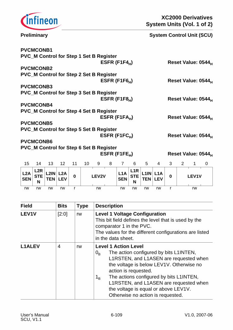
XC2000 DerivativesSystem Units (Vol. 1 of 2)
System Control Unit (SCU)Preliminary
PVCMCONB1PVC_M Control for Step 1 Set B Register
ESFR (F1F4H) Reset Value: 0544HPVCMCONB2PVC_M Control for Step 2 Set B Register
ESFR (F1F6H) Reset Value: 0544HPVCMCONB3PVC_M Control for Step 3 Set B Register
ESFR (F1F8H) Reset Value: 0544HPVCMCONB4PVC_M Control for Step 4 Set B Register
ESFR (F1FAH) Reset Value: 0544HPVCMCONB5PVC_M Control for Step 5 Set B Register
ESFR (F1FCH) Reset Value: 0544HPVCMCONB6PVC_M Control for Step 6 Set B Register
ESFR (F1FEH) Reset Value: 0544H
15 14 13 12 11 10 9 8 7 6 5 4 3 2 1 0
L2ASEN
L2RSTE
N
L2INTEN
L2ALEV 0 LEV2V L1A
SEN
L1RSTE
N
L1INTEN
L1ALEV 0 LEV1V
rw rw rw rw r rw rw rw rw rw r rw
Field Bits Type DescriptionLEV1V [2:0] rw Level 1 Voltage Configuration
This bit field defines the level that is used by the comparator 1 in the PVC.The values for the different configurations are listed in the data sheet.
L1ALEV 4 rw Level 1 Action Level0B The action configured by bits L1INTEN,
L1RSTEN, and L1ASEN are requested when the voltage is below LEV1V. Otherwise no action is requested.
1B The actions configured by bits L1INTEN, L1RSTEN, and L1ASEN are requested when the voltage is equal or above LEV1V. Otherwise no action is requested.
User’s Manual 6-109 V1.0, 2007-06SCU, V1.1

XC2000 DerivativesSystem Units (Vol. 1 of 2)
System Control Unit (SCU)Preliminary
L1INTEN 5 rw Level 1 Interrupt Request EnableThis bit defines if an interrupt request trigger is requested if the comparison level check was successful. When a check is successful is defined via bit L1ALEV.0B No interrupt is requested1B An interrupt is requested
L1RSTEN 6 rw Level 1 Reset Request EnableThis bit defines if an reset request trigger is requested if the comparison level check was successful. When a check is successful is defined via bit L1ALEV.0B No reset is requested1B An reset is requested
L1ASEN 7 rw Level 1 Asynchronous Action EnableThis bit defines if asynchronous action can be performed if the comparison level check was successful. When a check is successful is defined via bit L1ALEV.0B No asynchronous actions are performed1B Asynchronous actions can be performed
LEV2V [10:8] rw Level 2 Voltage ConfigurationThis bit field defines the level that is used by the comparator 2 in the PVC.The values for the different configurations are listed in the data sheet.
L2ALEV 12 rw Level 2 Action Level0B The action configured by bits L2INTEN,
L2RSTEN, and L2ASEN are requested when the voltage is below LEV2V. Otherwise no action is requested.
1B The action configured by bits L2INTEN, L2RSTEN, and L2ASEN are requested when the voltage is equal or above LEV2V. Otherwise no action is requested.
Field Bits Type Description
User’s Manual 6-110 V1.0, 2007-06SCU, V1.1
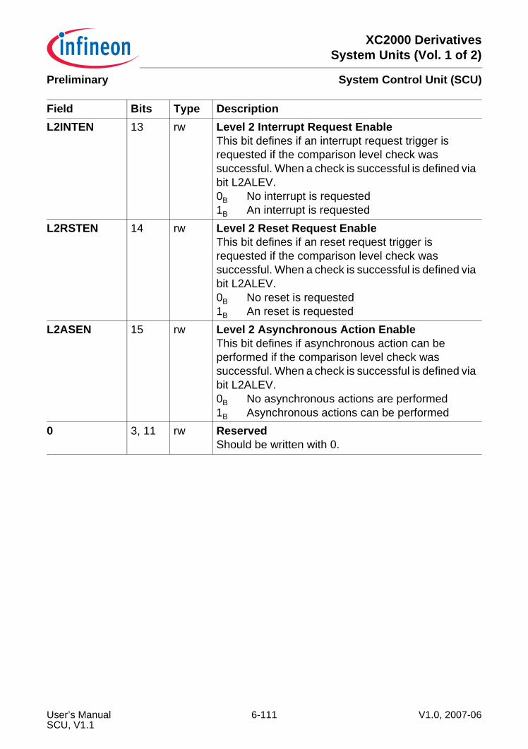
XC2000 DerivativesSystem Units (Vol. 1 of 2)
System Control Unit (SCU)Preliminary
L2INTEN 13 rw Level 2 Interrupt Request EnableThis bit defines if an interrupt request trigger is requested if the comparison level check was successful. When a check is successful is defined via bit L2ALEV.0B No interrupt is requested1B An interrupt is requested
L2RSTEN 14 rw Level 2 Reset Request EnableThis bit defines if an reset request trigger is requested if the comparison level check was successful. When a check is successful is defined via bit L2ALEV.0B No reset is requested1B An reset is requested
L2ASEN 15 rw Level 2 Asynchronous Action EnableThis bit defines if asynchronous action can be performed if the comparison level check was successful. When a check is successful is defined via bit L2ALEV.0B No asynchronous actions are performed1B Asynchronous actions can be performed
0 3, 11 rw ReservedShould be written with 0.
Field Bits Type Description
User’s Manual 6-111 V1.0, 2007-06SCU, V1.1
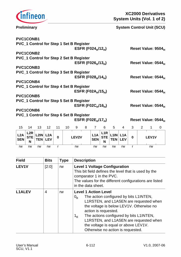
XC2000 DerivativesSystem Units (Vol. 1 of 2)
System Control Unit (SCU)Preliminary
PVC1CONB1PVC_1 Control for Step 1 Set B Register
ESFR (F024H/12H) Reset Value: 9504HPVC1CONB2PVC_1 Control for Step 2 Set B Register
ESFR (F026H/13H) Reset Value: 0544HPVC1CONB3PVC_1 Control for Step 3 Set B Register
ESFR (F028H/14H) Reset Value: 0544HPVC1CONB4PVC_1 Control for Step 4 Set B Register
ESFR (F02AH/15H) Reset Value: 0544HPVC1CONB5PVC_1 Control for Step 5 Set B Register
ESFR (F02CH/16H) Reset Value: 0544HPVC1CONB6PVC_1 Control for Step 6 Set B Register
ESFR (F02EH/17H) Reset Value: 0544H
15 14 13 12 11 10 9 8 7 6 5 4 3 2 1 0
L2ASEN
L2RSTE
N
L2INTEN
L2ALEV 0 LEV2V L1A
SEN
L1RSTE
N
L1INTEN
L1ALEV 0 LEV1V
rw rw rw rw r rw rw rw rw rw r rw
Field Bits Type DescriptionLEV1V [2:0] rw Level 1 Voltage Configuration
This bit field defines the level that is used by the comparator 1 in the PVC.The values for the different configurations are listed in the data sheet.
L1ALEV 4 rw Level 1 Action Level0B The action configured by bits L1INTEN,
L1RSTEN, and L1ASEN are requested when the voltage is below LEV1V. Otherwise no action is requested.
1B The actions configured by bits L1INTEN, L1RSTEN, and L1ASEN are requested when the voltage is equal or above LEV1V. Otherwise no action is requested.
User’s Manual 6-112 V1.0, 2007-06SCU, V1.1
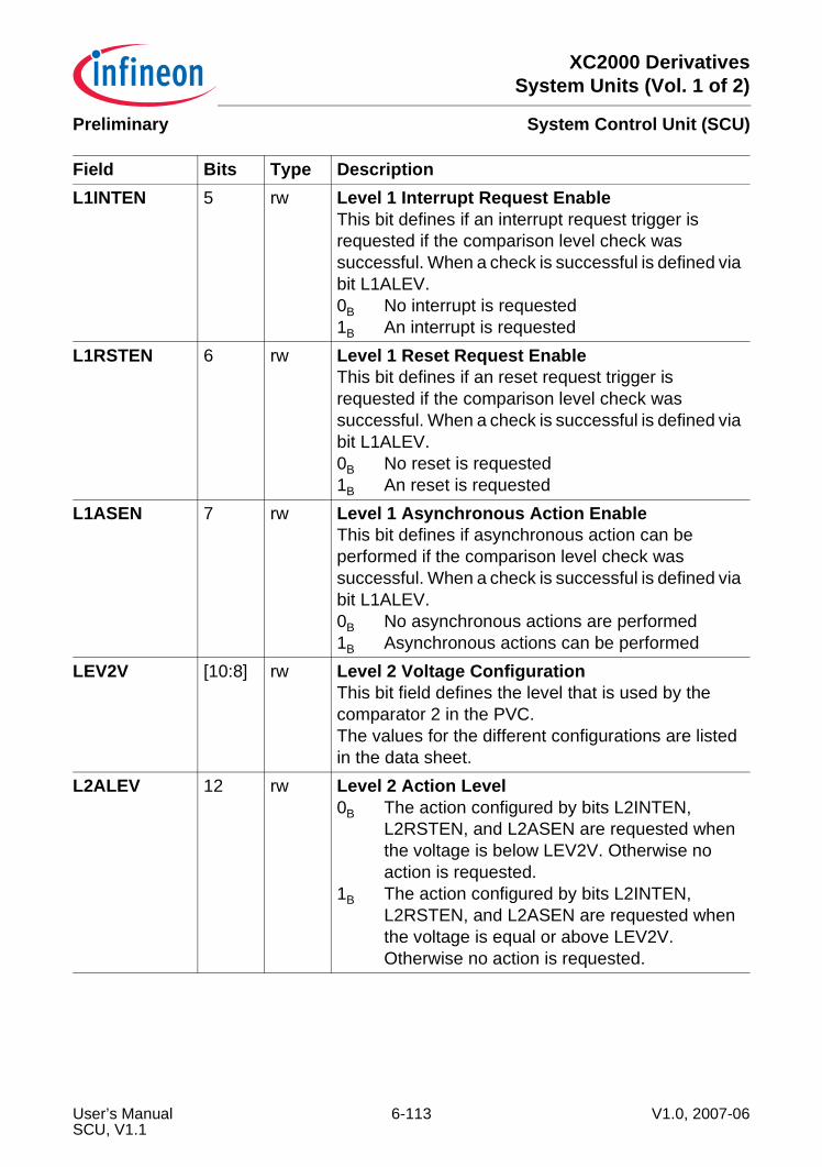
XC2000 DerivativesSystem Units (Vol. 1 of 2)
System Control Unit (SCU)Preliminary
L1INTEN 5 rw Level 1 Interrupt Request EnableThis bit defines if an interrupt request trigger is requested if the comparison level check was successful. When a check is successful is defined via bit L1ALEV.0B No interrupt is requested1B An interrupt is requested
L1RSTEN 6 rw Level 1 Reset Request EnableThis bit defines if an reset request trigger is requested if the comparison level check was successful. When a check is successful is defined via bit L1ALEV.0B No reset is requested1B An reset is requested
L1ASEN 7 rw Level 1 Asynchronous Action EnableThis bit defines if asynchronous action can be performed if the comparison level check was successful. When a check is successful is defined via bit L1ALEV.0B No asynchronous actions are performed1B Asynchronous actions can be performed
LEV2V [10:8] rw Level 2 Voltage ConfigurationThis bit field defines the level that is used by the comparator 2 in the PVC.The values for the different configurations are listed in the data sheet.
L2ALEV 12 rw Level 2 Action Level0B The action configured by bits L2INTEN,
L2RSTEN, and L2ASEN are requested when the voltage is below LEV2V. Otherwise no action is requested.
1B The action configured by bits L2INTEN, L2RSTEN, and L2ASEN are requested when the voltage is equal or above LEV2V. Otherwise no action is requested.
Field Bits Type Description
User’s Manual 6-113 V1.0, 2007-06SCU, V1.1

XC2000 DerivativesSystem Units (Vol. 1 of 2)
System Control Unit (SCU)Preliminary
L2INTEN 13 rw Level 2 Interrupt Request EnableThis bit defines if an interrupt request trigger is requested if the comparison level check was successful. When a check is successful is defined via bit L2ALEV.0B No interrupt is requested1B An interrupt is requested
L2RSTEN 14 rw Level 2 Reset Request EnableThis bit defines if an reset request trigger is requested if the comparison level check was successful. When a check is successful is defined via bit L2ALEV.0B No reset is requested1B An reset is requested
L2ASEN 15 rw Level 2 Asynchronous Action EnableThis bit defines if asynchronous action can be performed if the comparison level check was successful. When a check is successful is defined via bit L2ALEV.0B No asynchronous actions are performed1B Asynchronous actions can be performed
0 3, 11 rw ReservedShould be written with 0.
Field Bits Type Description
User’s Manual 6-114 V1.0, 2007-06SCU, V1.1
XC2000 DerivativesSystem Units (Vol. 1 of 2)
System Control Unit (SCU)Preliminary
6.5.3 Controlling the Voltage Level of a Core DomainThe two core power domains DMP_M and DMP_1 can be controlled individually withincertain limits. The limits are defined by the supported Power States. The voltage levelof each core domain is controlled by an own Embedded Voltage Regulator (EVR).The core power domain DMP_M is control by the EVR_M.The core power domain DMP_1 is control by the EVR_1.
6.5.3.1 Power StatesBased on the various operating states of the EVRs, several Power Modes are defined inorder to achieve easily a power reduction.Table 6-14 summarizes the power states based on the respective voltage levels.
6.5.3.2 Embedded Voltage RegulatorAn embedded voltage regulator (EVR) provides an stable core supply voltage
Feature list:• Regulation with external buffer capacitor• Selectable core voltage levels, including zero• Core voltage generation either based on a Low Power Reference or on a High
Precision Bandgap• External supply possible via capacitor-pin while EVR is offWhen the EVR is disabled it tolerate an external supply voltage provided through the pinVDDI that connects the external buffer capacitor.The EVR configurations to select the desired voltage and reference pair are combinedwithin EVR settings EVRxSETyyV (x = M or 1 and yy = 10 or 15). Each setting containsa bit field (VRSEL) to select the voltage level and reference and a bit field to fine-tunethe voltage level (VLEV). One out of the possible settings is used to control each of theEVRs, but only in the allowed combinations for the two EVRs. The core voltagegenerated by an EVR is derived either from the Low Power Reference (LPR) or from theHigh Precision Bandgap (HP).
Table 6-14 Operating States Based on Supply VoltageDMP_1
DMP_M Off Reduced Voltage Full VoltageReduced Voltage
Power State A Power State B Not Allowed
Full Voltage Power State F Power State G Power State I
User’s Manual 6-115 V1.0, 2007-06SCU, V1.1
XC2000 DerivativesSystem Units (Vol. 1 of 2)
System Control Unit (SCU)Preliminary
The core voltage of each setting can be adjusted to compensate application andenvironmental influences. This is control via bit field EVRxSETyyV.VLEV.
Lower Power Reference (LPR)The LPR of an EVR is used for two purposes:• Operation in a Power State other than Full Active• Special Power Saving in the Full Active Power StateThe LPR can be enabled / disabled via the bit EVRxSETyyV.LPRDIS. If a setting use theLPR or not is defined via the bit field EVRxSETyyV.VRSEL. Please note that even if bitEVRxSETyyV.LPRDIS and the bit field EVRxSETyyV.VRVAL are writable this shouldnot be done, the reset value of the setting registers is already defined in the way thedifferent setting work.As the core voltage depends on the LPR the LPR can be adjusted via bit fieldEVRxCON0.LPRLEV for application specific fine tuning.
High Precision Bandgap (HP)The HP bandgap of the system is used for two purposes:• Provide a very stable reference for the two EVRs when operating in Full Active• Provide a reference for the flash memory. For more information about this point see
the flash memory description.Only one HP bandgap is implemented which is used by both EVRs. The HP bandgapcan be enabled / disable via the bit EVRMCON1.HPEN.As the core voltage depends on the HP configuration, the HP bandgap can be adjustedvia bit field EVRMCON1.HPADJUST for application specific fine tuning.
User’s Manual 6-116 V1.0, 2007-06SCU, V1.1
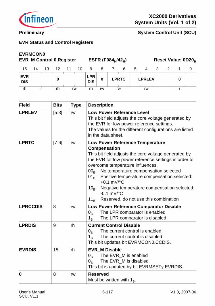
XC2000 DerivativesSystem Units (Vol. 1 of 2)
System Control Unit (SCU)Preliminary
EVR Status and Control Registers
EVRMCON0EVR_M Control 0 Register ESFR (F084H/42H) Reset Value: 0D20H
15 14 13 12 11 10 9 8 7 6 5 4 3 2 1 0
EVRDIS 0 LPR
DIS 0 LPRTC LPRLEV 0
rh r rh rw rh rw rw rw r
Field Bits Type DescriptionLPRLEV [5:3] rw Low Power Reference Level
This bit field adjusts the core voltage generated by the EVR for low power reference settings.The values for the different configurations are listed in the data sheet.
LPRTC [7:6] rw Low Power Reference Temperature CompensationThis bit field adjusts the core voltage generated by the EVR for low power reference settings in order to overcome temperature influences.00B No temperature compensation selected01B Positive temperature compensation selected:
+0.1 mV/°C10B Negative temperature compensation selected:
-0.1 mV/°C11B Reserved, do not use this combination
LPRCCDIS 8 rw Low Power Reference Comparator Disable0B The LPR comparator is enabled1B The LPR comparator is disabled
LPRDIS 9 rh Current Control Disable0B The current control is enabled1B The current control is disabledThis bit updates bit EVRMCON0.CCDIS.
EVRDIS 15 rh EVR_M Disable0B The EVR_M is enabled0B The EVR_M is disabledThis bit is updated by bit EVRMSETy.EVRDIS.
0 8 rw ReservedMust be written with 1B.
User’s Manual 6-117 V1.0, 2007-06SCU, V1.1
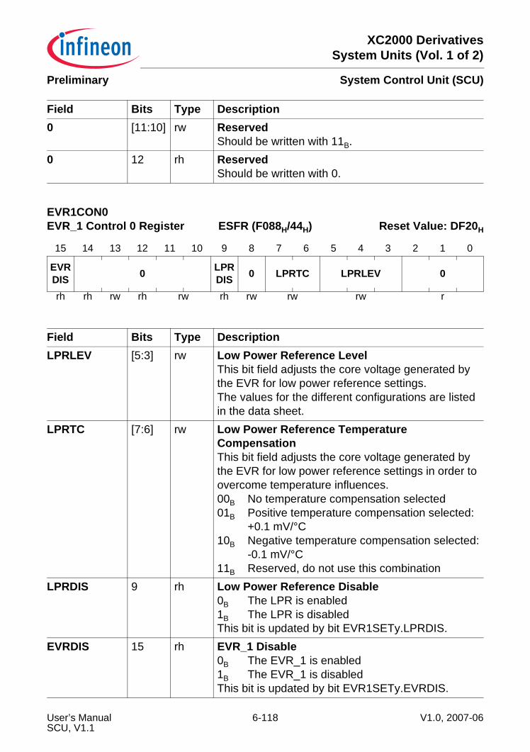
XC2000 DerivativesSystem Units (Vol. 1 of 2)
System Control Unit (SCU)Preliminary
0 [11:10] rw ReservedShould be written with 11B.
0 12 rh ReservedShould be written with 0.
EVR1CON0EVR_1 Control 0 Register ESFR (F088H/44H) Reset Value: DF20H
15 14 13 12 11 10 9 8 7 6 5 4 3 2 1 0
EVRDIS 0 LPR
DIS 0 LPRTC LPRLEV 0
rh rh rw rh rw rh rw rw rw r
Field Bits Type DescriptionLPRLEV [5:3] rw Low Power Reference Level
This bit field adjusts the core voltage generated by the EVR for low power reference settings.The values for the different configurations are listed in the data sheet.
LPRTC [7:6] rw Low Power Reference Temperature CompensationThis bit field adjusts the core voltage generated by the EVR for low power reference settings in order to overcome temperature influences.00B No temperature compensation selected01B Positive temperature compensation selected:
+0.1 mV/°C10B Negative temperature compensation selected:
-0.1 mV/°C11B Reserved, do not use this combination
LPRDIS 9 rh Low Power Reference Disable0B The LPR is enabled1B The LPR is disabledThis bit is updated by bit EVR1SETy.LPRDIS.
EVRDIS 15 rh EVR_1 Disable0B The EVR_1 is enabled1B The EVR_1 is disabledThis bit is updated by bit EVR1SETy.EVRDIS.
Field Bits Type Description
User’s Manual 6-118 V1.0, 2007-06SCU, V1.1
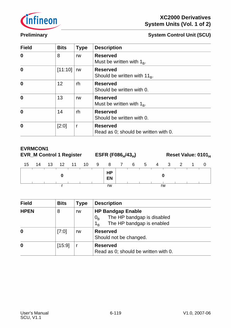
XC2000 DerivativesSystem Units (Vol. 1 of 2)
System Control Unit (SCU)Preliminary
0 8 rw ReservedMust be written with 1B.
0 [11:10] rw ReservedShould be written with 11B.
0 12 rh ReservedShould be written with 0.
0 13 rw ReservedMust be written with 1B.
0 14 rh ReservedShould be written with 0.
0 [2:0] r ReservedRead as 0; should be written with 0.
EVRMCON1EVR_M Control 1 Register ESFR (F086H/43H) Reset Value: 0101H
15 14 13 12 11 10 9 8 7 6 5 4 3 2 1 0
0 HPEN 0
r rw rw
Field Bits Type DescriptionHPEN 8 rw HP Bandgap Enable
0B The HP bandgap is disabled1B The HP bandgap is enabled
0 [7:0] rw ReservedShould not be changed.
0 [15:9] r ReservedRead as 0; should be written with 0.
Field Bits Type Description
User’s Manual 6-119 V1.0, 2007-06SCU, V1.1

XC2000 DerivativesSystem Units (Vol. 1 of 2)
System Control Unit (SCU)Preliminary
EVRMSET10VEVR_M Setting for 1.0 V Register
ESFR (F090H/48H) Reset Value: 005BH
15 14 13 12 11 10 9 8 7 6 5 4 3 2 1 0
EVRDIS 0 CC
DIS 0 LPRDIS 0 VRSEL VLEV
rw rw rw rw rw rw rw rw
Field Bits Type DescriptionVLEV [5:0] rw Voltage Level Adjust
The values for the different configurations are listed in the data sheet.
VRSEL [7:6] rw Voltage Reference Selection00B Full Voltage with high precision bandgap
selected01B Reduced Voltage with low power reference
selected10B Reserved, done not use this combination11B Full Voltage with low power reference selectedNote: 01B should always be written to this bit field.
LPRDIS 9 rw Low Power Reference Disable0B The LPR is enabled1B The LPR is disabledThis bit updates bit EVRMCON0.LPRDIS.
CCDIS 12 rw Current Control Disable0B The current control is enabled1B The current control is disabledThis bit updates bit EVRMCON0.CCDIS.
EVRDIS 15 rw EVR_M Disable0B The EVR_M is enabled1B The EVR_M is disabledThis bit updates bit EVRMCON0.EVRDIS.
0 8,[11:10][14:13]
rw ReservedShould be written with 0.
User’s Manual 6-120 V1.0, 2007-06SCU, V1.1
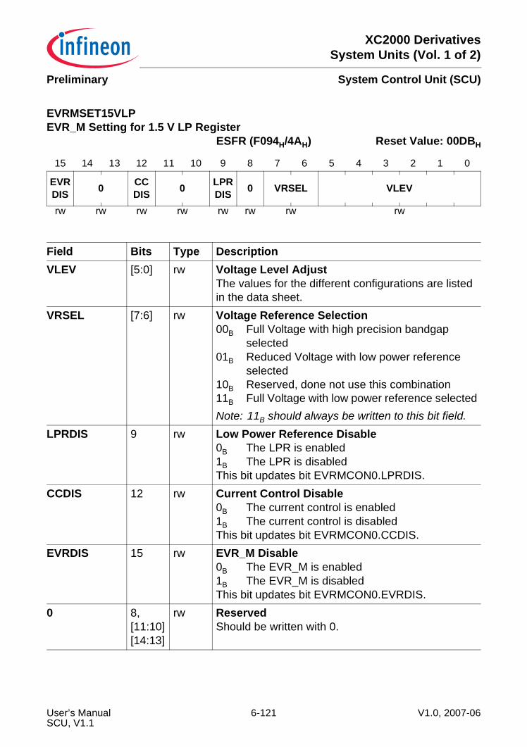
XC2000 DerivativesSystem Units (Vol. 1 of 2)
System Control Unit (SCU)Preliminary
EVRMSET15VLPEVR_M Setting for 1.5 V LP Register
ESFR (F094H/4AH) Reset Value: 00DBH
15 14 13 12 11 10 9 8 7 6 5 4 3 2 1 0
EVRDIS 0 CC
DIS 0 LPRDIS 0 VRSEL VLEV
rw rw rw rw rw rw rw rw
Field Bits Type DescriptionVLEV [5:0] rw Voltage Level Adjust
The values for the different configurations are listed in the data sheet.
VRSEL [7:6] rw Voltage Reference Selection00B Full Voltage with high precision bandgap
selected01B Reduced Voltage with low power reference
selected10B Reserved, done not use this combination11B Full Voltage with low power reference selectedNote: 11B should always be written to this bit field.
LPRDIS 9 rw Low Power Reference Disable0B The LPR is enabled1B The LPR is disabledThis bit updates bit EVRMCON0.LPRDIS.
CCDIS 12 rw Current Control Disable0B The current control is enabled1B The current control is disabledThis bit updates bit EVRMCON0.CCDIS.
EVRDIS 15 rw EVR_M Disable0B The EVR_M is enabled1B The EVR_M is disabledThis bit updates bit EVRMCON0.EVRDIS.
0 8,[11:10][14:13]
rw ReservedShould be written with 0.
User’s Manual 6-121 V1.0, 2007-06SCU, V1.1
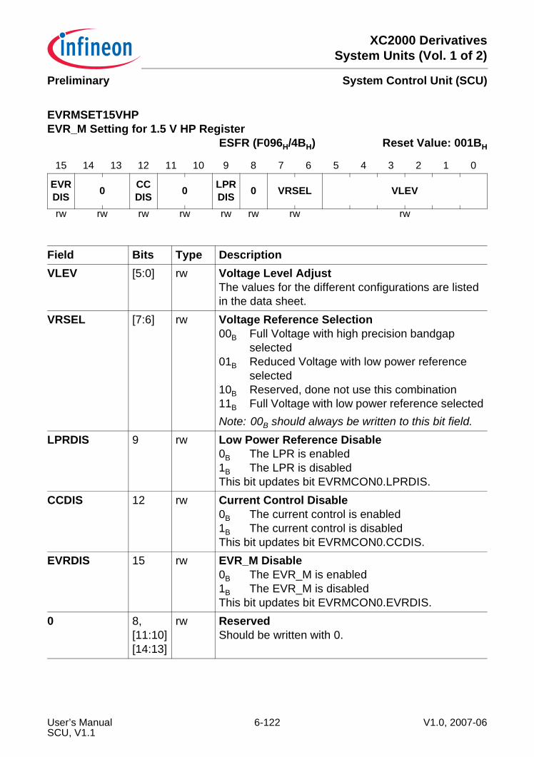
XC2000 DerivativesSystem Units (Vol. 1 of 2)
System Control Unit (SCU)Preliminary
EVRMSET15VHPEVR_M Setting for 1.5 V HP Register
ESFR (F096H/4BH) Reset Value: 001BH
15 14 13 12 11 10 9 8 7 6 5 4 3 2 1 0
EVRDIS 0 CC
DIS 0 LPRDIS 0 VRSEL VLEV
rw rw rw rw rw rw rw rw
Field Bits Type DescriptionVLEV [5:0] rw Voltage Level Adjust
The values for the different configurations are listed in the data sheet.
VRSEL [7:6] rw Voltage Reference Selection00B Full Voltage with high precision bandgap
selected01B Reduced Voltage with low power reference
selected10B Reserved, done not use this combination11B Full Voltage with low power reference selectedNote: 00B should always be written to this bit field.
LPRDIS 9 rw Low Power Reference Disable0B The LPR is enabled1B The LPR is disabledThis bit updates bit EVRMCON0.LPRDIS.
CCDIS 12 rw Current Control Disable0B The current control is enabled1B The current control is disabledThis bit updates bit EVRMCON0.CCDIS.
EVRDIS 15 rw EVR_M Disable0B The EVR_M is enabled1B The EVR_M is disabledThis bit updates bit EVRMCON0.EVRDIS.
0 8,[11:10][14:13]
rw ReservedShould be written with 0.
User’s Manual 6-122 V1.0, 2007-06SCU, V1.1
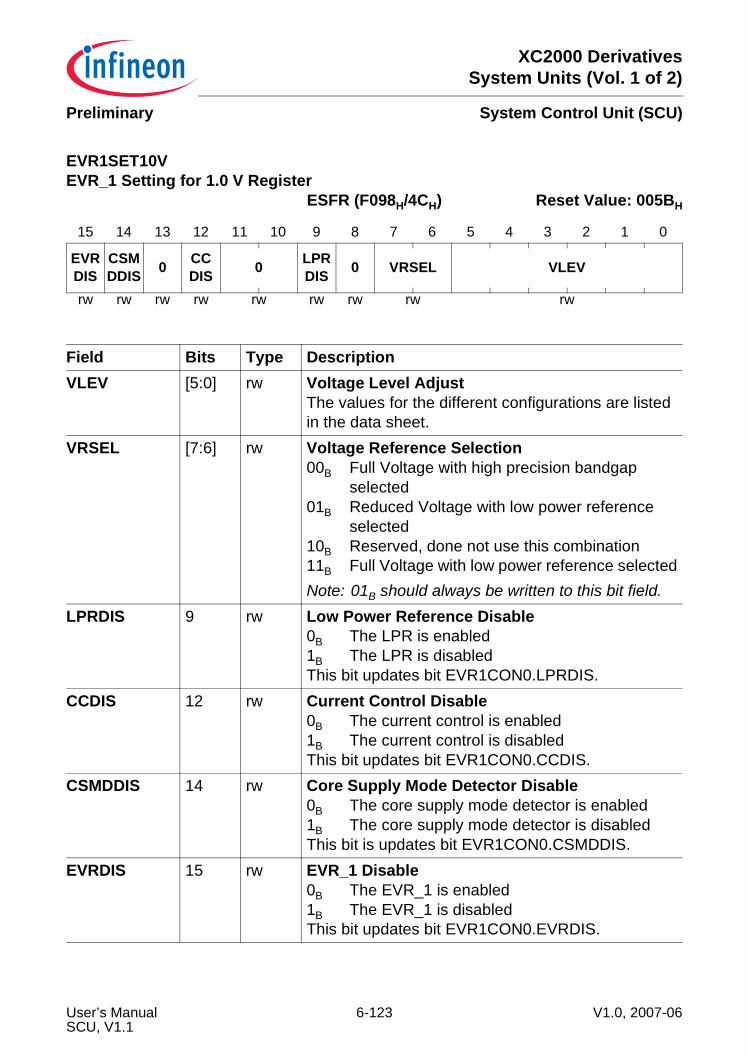
XC2000 DerivativesSystem Units (Vol. 1 of 2)
System Control Unit (SCU)Preliminary
EVR1SET10VEVR_1 Setting for 1.0 V Register
ESFR (F098H/4CH) Reset Value: 005BH
15 14 13 12 11 10 9 8 7 6 5 4 3 2 1 0
EVRDIS
CSMDDIS 0 CC
DIS 0 LPRDIS 0 VRSEL VLEV
rw rw rw rw rw rw rw rw rw
Field Bits Type DescriptionVLEV [5:0] rw Voltage Level Adjust
The values for the different configurations are listed in the data sheet.
VRSEL [7:6] rw Voltage Reference Selection00B Full Voltage with high precision bandgap
selected01B Reduced Voltage with low power reference
selected10B Reserved, done not use this combination11B Full Voltage with low power reference selectedNote: 01B should always be written to this bit field.
LPRDIS 9 rw Low Power Reference Disable0B The LPR is enabled1B The LPR is disabledThis bit updates bit EVR1CON0.LPRDIS.
CCDIS 12 rw Current Control Disable0B The current control is enabled1B The current control is disabledThis bit updates bit EVR1CON0.CCDIS.
CSMDDIS 14 rw Core Supply Mode Detector Disable0B The core supply mode detector is enabled1B The core supply mode detector is disabledThis bit is updates bit EVR1CON0.CSMDDIS.
EVRDIS 15 rw EVR_1 Disable0B The EVR_1 is enabled1B The EVR_1 is disabledThis bit updates bit EVR1CON0.EVRDIS.
User’s Manual 6-123 V1.0, 2007-06SCU, V1.1
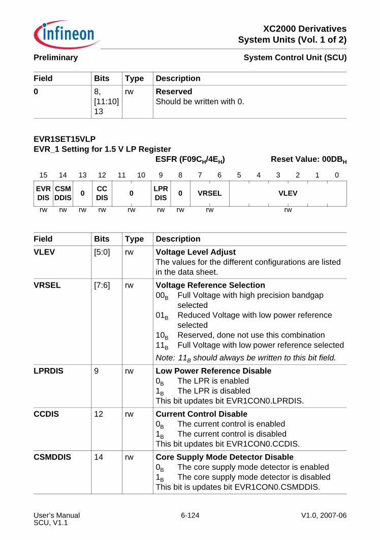
XC2000 DerivativesSystem Units (Vol. 1 of 2)
System Control Unit (SCU)Preliminary
0 8,[11:10]13
rw ReservedShould be written with 0.
EVR1SET15VLPEVR_1 Setting for 1.5 V LP Register
ESFR (F09CH/4EH) Reset Value: 00DBH
15 14 13 12 11 10 9 8 7 6 5 4 3 2 1 0
EVRDIS
CSMDDIS 0 CC
DIS 0 LPRDIS 0 VRSEL VLEV
rw rw rw rw rw rw rw rw rw
Field Bits Type DescriptionVLEV [5:0] rw Voltage Level Adjust
The values for the different configurations are listed in the data sheet.
VRSEL [7:6] rw Voltage Reference Selection00B Full Voltage with high precision bandgap
selected01B Reduced Voltage with low power reference
selected10B Reserved, done not use this combination11B Full Voltage with low power reference selectedNote: 11B should always be written to this bit field.
LPRDIS 9 rw Low Power Reference Disable0B The LPR is enabled1B The LPR is disabledThis bit updates bit EVR1CON0.LPRDIS.
CCDIS 12 rw Current Control Disable0B The current control is enabled1B The current control is disabledThis bit updates bit EVR1CON0.CCDIS.
CSMDDIS 14 rw Core Supply Mode Detector Disable0B The core supply mode detector is enabled1B The core supply mode detector is disabledThis bit is updates bit EVR1CON0.CSMDDIS.
Field Bits Type Description
User’s Manual 6-124 V1.0, 2007-06SCU, V1.1
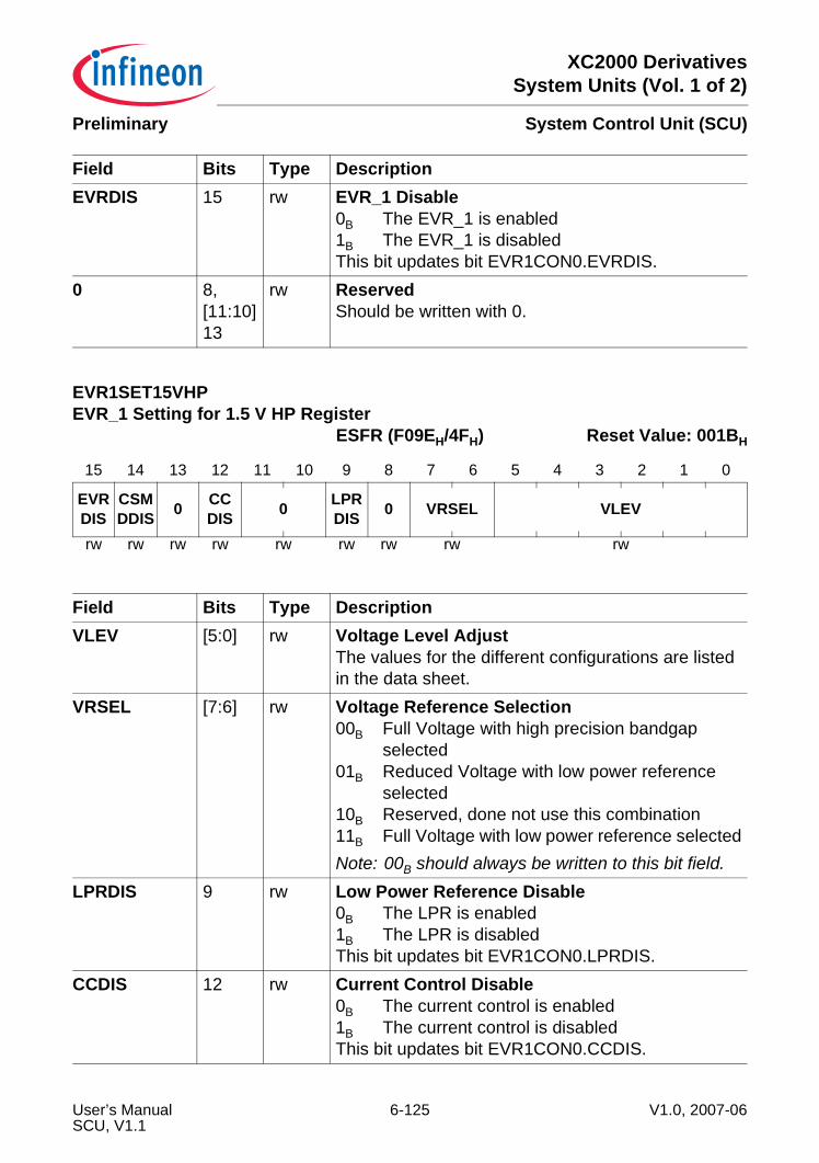
XC2000 DerivativesSystem Units (Vol. 1 of 2)
System Control Unit (SCU)Preliminary
EVRDIS 15 rw EVR_1 Disable0B The EVR_1 is enabled1B The EVR_1 is disabledThis bit updates bit EVR1CON0.EVRDIS.
0 8,[11:10]13
rw ReservedShould be written with 0.
EVR1SET15VHPEVR_1 Setting for 1.5 V HP Register
ESFR (F09EH/4FH) Reset Value: 001BH
15 14 13 12 11 10 9 8 7 6 5 4 3 2 1 0
EVRDIS
CSMDDIS 0 CC
DIS 0 LPRDIS 0 VRSEL VLEV
rw rw rw rw rw rw rw rw rw
Field Bits Type DescriptionVLEV [5:0] rw Voltage Level Adjust
The values for the different configurations are listed in the data sheet.
VRSEL [7:6] rw Voltage Reference Selection00B Full Voltage with high precision bandgap
selected01B Reduced Voltage with low power reference
selected10B Reserved, done not use this combination11B Full Voltage with low power reference selectedNote: 00B should always be written to this bit field.
LPRDIS 9 rw Low Power Reference Disable0B The LPR is enabled1B The LPR is disabledThis bit updates bit EVR1CON0.LPRDIS.
CCDIS 12 rw Current Control Disable0B The current control is enabled1B The current control is disabledThis bit updates bit EVR1CON0.CCDIS.
Field Bits Type Description
User’s Manual 6-125 V1.0, 2007-06SCU, V1.1
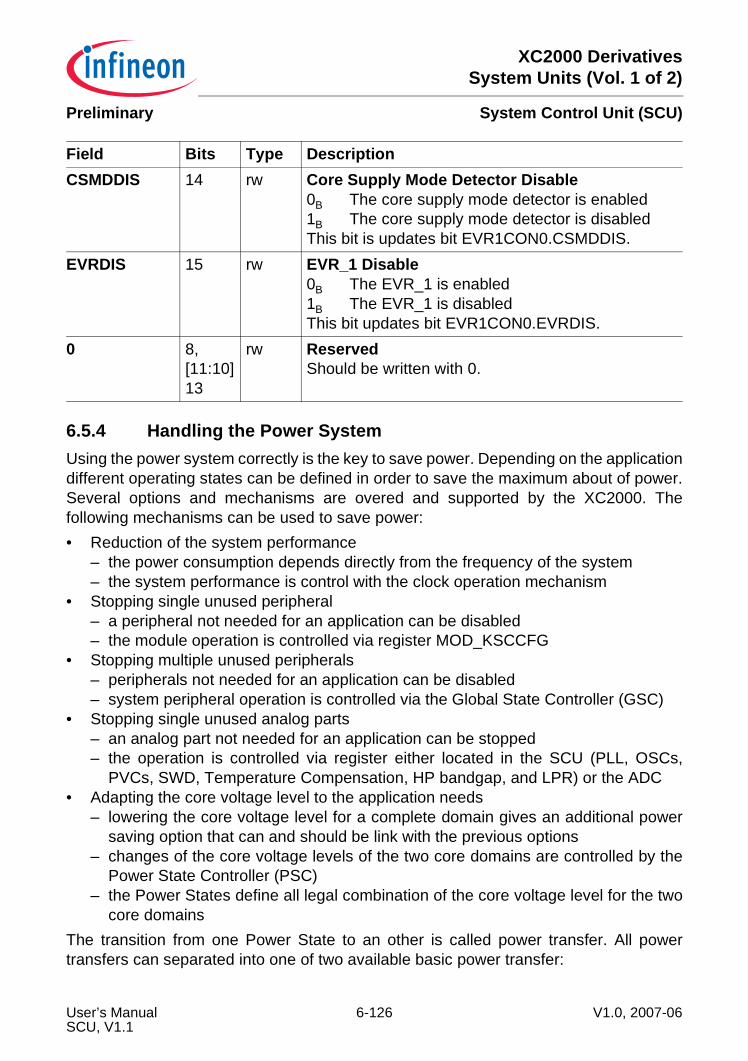
XC2000 DerivativesSystem Units (Vol. 1 of 2)
System Control Unit (SCU)Preliminary
6.5.4 Handling the Power SystemUsing the power system correctly is the key to save power. Depending on the applicationdifferent operating states can be defined in order to save the maximum about of power.Several options and mechanisms are overed and supported by the XC2000. Thefollowing mechanisms can be used to save power:• Reduction of the system performance
– the power consumption depends directly from the frequency of the system– the system performance is control with the clock operation mechanism
• Stopping single unused peripheral– a peripheral not needed for an application can be disabled– the module operation is controlled via register MOD_KSCCFG
• Stopping multiple unused peripherals– peripherals not needed for an application can be disabled– system peripheral operation is controlled via the Global State Controller (GSC)
• Stopping single unused analog parts– an analog part not needed for an application can be stopped– the operation is controlled via register either located in the SCU (PLL, OSCs,
PVCs, SWD, Temperature Compensation, HP bandgap, and LPR) or the ADC• Adapting the core voltage level to the application needs
– lowering the core voltage level for a complete domain gives an additional powersaving option that can and should be link with the previous options
– changes of the core voltage levels of the two core domains are controlled by thePower State Controller (PSC)
– the Power States define all legal combination of the core voltage level for the twocore domains
The transition from one Power State to an other is called power transfer. All powertransfers can separated into one of two available basic power transfer:
CSMDDIS 14 rw Core Supply Mode Detector Disable0B The core supply mode detector is enabled1B The core supply mode detector is disabledThis bit is updates bit EVR1CON0.CSMDDIS.
EVRDIS 15 rw EVR_1 Disable0B The EVR_1 is enabled1B The EVR_1 is disabledThis bit updates bit EVR1CON0.EVRDIS.
0 8,[11:10]13
rw ReservedShould be written with 0.
Field Bits Type Description
User’s Manual 6-126 V1.0, 2007-06SCU, V1.1
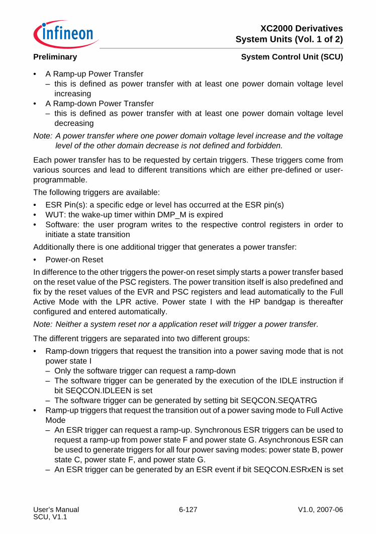
XC2000 DerivativesSystem Units (Vol. 1 of 2)
System Control Unit (SCU)Preliminary
• A Ramp-up Power Transfer– this is defined as power transfer with at least one power domain voltage level
increasing• A Ramp-down Power Transfer
– this is defined as power transfer with at least one power domain voltage leveldecreasing
Note: A power transfer where one power domain voltage level increase and the voltagelevel of the other domain decrease is not defined and forbidden.
Each power transfer has to be requested by certain triggers. These triggers come fromvarious sources and lead to different transitions which are either pre-defined or user-programmable.The following triggers are available:• ESR Pin(s): a specific edge or level has occurred at the ESR pin(s)• WUT: the wake-up timer within DMP_M is expired• Software: the user program writes to the respective control registers in order to
initiate a state transitionAdditionally there is one additional trigger that generates a power transfer:• Power-on ResetIn difference to the other triggers the power-on reset simply starts a power transfer basedon the reset value of the PSC registers. The power transition itself is also predefined andfix by the reset values of the EVR and PSC registers and lead automatically to the FullActive Mode with the LPR active. Power state I with the HP bandgap is thereafterconfigured and entered automatically.Note: Neither a system reset nor a application reset will trigger a power transfer.
The different triggers are separated into two different groups:• Ramp-down triggers that request the transition into a power saving mode that is not
power state I– Only the software trigger can request a ramp-down– The software trigger can be generated by the execution of the IDLE instruction if
bit SEQCON.IDLEEN is set– The software trigger can be generated by setting bit SEQCON.SEQATRG
• Ramp-up triggers that request the transition out of a power saving mode to Full ActiveMode– An ESR trigger can request a ramp-up. Synchronous ESR triggers can be used to
request a ramp-up from power state F and power state G. Asynchronous ESR canbe used to generate triggers for all four power saving modes: power state B, powerstate C, power state F, and power state G.
– An ESR trigger can be generated by an ESR event if bit SEQCON.ESRxEN is set
User’s Manual 6-127 V1.0, 2007-06SCU, V1.1
XC2000 DerivativesSystem Units (Vol. 1 of 2)
System Control Unit (SCU)Preliminary
– A wake-up timer event can generate a ramp-up trigger. A wake-up timer triggercan request a ramp-up from the power saving states power state F and powerstate G only.
– A wake-up timer trigger can be generated by an WUT event if bitSEQCON.WUTEN is set
6.5.5 Power State Controller (PSC)The Power State Controller (PSC) controls the operation of the EVRs and PVCs andhandles changes in the control different values.
6.5.5.1 General OverviewA power state transition implies a change of the core voltages in one or both core supplydomains. Each power state transition consists of several steps to de-couple the differentphases of the State Transition Sequence (STS). A state transition sequence defines howEVRs and their associated PVCs are controlled and modified when a voltage change isrequested from the system.• Sequence A is used for ramp-down power transfers• Sequence B is used for ramp-up power transfersSequence A; it is invoked if instruction IDLE is executed or a software trigger bitSEQBTRG in register SEQCON is set.Sequence B; it is invoked if at least one valid wake-up trigger is asserted. If a wake-uptrigger is valid (can be recognized) depends on the currently entered power state. Forsequence B it is required to be pre-configured by the software when a power saving stateis entered where no software can be executed. Sequence B can only started after asequence A was performed. If no sequence A was performed the trigger for thesequence B is treated as pending as long as a sequence A was performed.Before a power transition is started all reset triggers that can request a reset have to bedisabled to ensure a correct power transition. Reset generation can be disabled bysetting RSTCON0 = 0x0000 and RSTCON1 = 0x0000. After the power transition thereset can be enabled again as the application requires. Due to the fact that for the powersaving states no software can be executed the resets remain disabled until power stateFull Active is entered again. For real emergency reset request that will cause seversystem damage when lost, they should be redirected to the PORST pin. Other resettriggers can either be redirected to a trap or the wake-up trigger of the power controlsystem via the ESR pins.
6.5.5.2 Sequence ConfigurationEach of the two sequences is built of six configuration data sets defining up to six steps.Each step of the sequence is controlled by its dedicated configuration data set.
User’s Manual 6-128 V1.0, 2007-06SCU, V1.1

XC2000 DerivativesSystem Units (Vol. 1 of 2)
System Control Unit (SCU)Preliminary
Step0 defines the current power state depending if the last transition was done withsequence A or sequence B. Step0 defines the target power state depending on thetransition type. The sets 1 to 6 can be used as interim step configurations that areneeded for a transition.At the end of each power state transition the values from the last enabled step are copiedto step 0.
6.5.5.3 Power State Transition ControllingThe PSC have to be pre-configured before the transition sequence is started. For apower state transition sequence using sequence B the control registers SEQBSTEPxand PVCyCONBx should be pre-configured for the wake-up transition before the firstpower state transition is stated.A transition sequence is started if either the IDLE instruction is executed or a ramp-uptrigger is asserted. A transition sequence is only started if no transition is currentlyrunning. The transition sequence itself is the controlled by the sequence control registersSEQzCONx.Note: With the start of a sequence a trigger for the WUT is generated. Therefore the
WUT can be started if configured so (WUCR.AON = 1).
Skipping a StepIf a step is skipped the next not skipped step is executed without any time penalty. If astep is skipped or not is configured via bit SEQzCONx.SEN.
Stopping the System Clock for a Power DomainIt is required to stop the system clock for each step that select a different core domainvoltage level than the previous step has for a power domain. If the core voltage levelsare unchanged the system clock can stay active. If the system clock has to be stoppedthe PSC requests so and for the continuation the asynchronous event has to beselected.If the system clock is not stopped synchronous continuation is selected.If the system clock is stopped asynchronous continuation is selected.This configuration is ignored if the step is configured to be skipped.The system clock is enabled again as soon as the selected trigger condition (bit fieldTRGSEL in the associated register) is valid again. If no trigger was selected(TRGSEL = 0000B) the system clock is not disabled at all.This feature is controlled via bits SEQzCONx.CLKEN1 and SEQzCONx.CLKENM
User’s Manual 6-129 V1.0, 2007-06SCU, V1.1
XC2000 DerivativesSystem Units (Vol. 1 of 2)
System Control Unit (SCU)Preliminary
Connection to the GSCIn order to stop or activate the operation of peripherals within DMP_1 the GSC is used.For this purpose the PSCx exit and PSCx entry GSC sources are used (x = sequence Aor B). If the system clock should be stopped for domain DMP_1 the PSCA entry is usedto bring all blocks in this domain into a state where the system clock can be stopped. Ifthe system clock should be active for domain DMP_1 the PSCB exit is used to reactivatethe clock system again. Unless disabled via bit SEQCON.GSCBY the entry request isgenerated at the start of a sequence (before the first step is executed). Unless disabledvia bit SEQCON.GSCBY the exit request is generated at the end of a sequence (afterthe last step is executed).
Asynchronous/Synchronous ContinuationAn asynchronous continuation event is defined if both selected PVC OK outputs (fromPVC_M and PVC_1) match their configured action level.A synchronous continuation event is defined by the system clock for DMP_M divided bythe value of bit field SEQzSTEPx.SYSDIV. Each time a step is started with the systemclock enabled for DMP_M a synchronous continuation trigger is generated after SYSDIVsystem clock cycles.Whenever the required continuation event occurs the next step is executed.This configuration is ignored if the step is configured to be skipped.
6.5.5.4 Trigger Handling during a Power TransitionA power transition is an atomic operation. This means that it has to be finished beforeany new active can be performed. Triggers that request an other power transitionoccurring a currently performed power transition are stored automatically and trigger thenext power transition immediately after the currently one is finished.
6.5.6 Operating a Power TransferPerforming a power transfer requires several steps that need to be executed involvingboth hardware and software operation. The main operation of each power transfer arethe power transitions handled by the PSC. Each power transfer includes exactly twopower transitions, one ramp-down followed by one ramp-up.
PreparationThis phase includes different tasks that are required to prepare the system for the ramp-down and the later ramp-up.• The sequence control register for both sequences A and B should be configured as
needed
User’s Manual 6-130 V1.0, 2007-06SCU, V1.1
XC2000 DerivativesSystem Units (Vol. 1 of 2)
System Control Unit (SCU)Preliminary
– The enable bits for the two power transitions should not be set before allpreparations are done in order to avoid a sequence start before the set-up isfinished
• The GSC control register should be set up to stop the operations for the ramp-downand restart of the operation with the ramp-up
• The KSCCFG control register of each module should be set up to stop the operationsfor the ramp-down and restart of the operation with the ramp-up
• The reset generation should be disable by clearing the RSTCON registers• The global interrupt disable should be set to avoid interrupt operation• OSC_WU has to be active• The wake-up timer should be configured if this trigger is intended as ramp-up trigger• The ESRx function should be configured if this trigger is intended as ramp-up trigger• The ESRx pads should be configured if this trigger is intended as ramp-up trigger• Switch to LPR operation and disable the HP bandgap if required by the application
– Disabling the HP bandgap for a power saving mode reduces the overall powerconsummation of this mode
– Disabling the HP bandgap also disables the flash, therefore all code that has to beexecuted afterwards till the flash active again has to be copied first to the PSRAM
• Switch off the VCO part of the PLL or the complete PLL– Disabling the VCO part or the complete PLL for a power saving mode reduces the
overall power consummation of this mode– Before disabling the VCO part or the complete PLL a clock source has to be
selected that still delivers a system clock after the VCO part or the complete PLLis disabled
• Enable both power sequences just before the IDLE instruction is executed• Execute the IDLE instruction
– The execution of the IDLE instruction starts the sequence A for the ramp-down
6.5.6.1 Generic Ramp-down ScenarioThe following scenario shows the ramp-down flow for a better understanding.Both thresholds are located below the current supply voltage. If the voltage falls belowthe higher threshold of the PVC, a warning interrupt can be generated (undershootwarning). If the voltage falls also below the lower threshold LEV1, a reset of this coresupply domain can be generated.1. Stop the system operation of the peripherals via the GSC2. Switch the power supply of the EVRs from the HP bandgap to the LPR if the HP
bandgap is currently used3. Start sequence A: Both threshold levels are changed. The reset level is changed to
the new target value - 100 mV and the old interrupt level is changed to the new targetlevel + 200 mV.
User’s Manual 6-131 V1.0, 2007-06SCU, V1.1
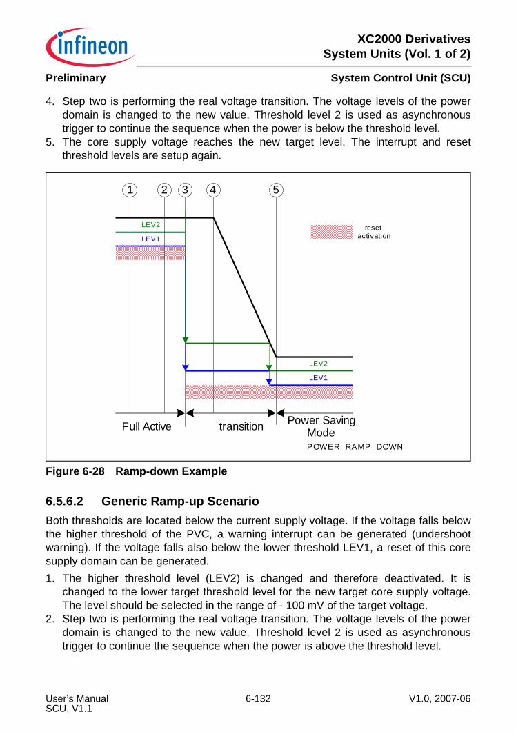
XC2000 DerivativesSystem Units (Vol. 1 of 2)
System Control Unit (SCU)Preliminary
4. Step two is performing the real voltage transition. The voltage levels of the powerdomain is changed to the new value. Threshold level 2 is used as asynchronoustrigger to continue the sequence when the power is below the threshold level.
5. The core supply voltage reaches the new target level. The interrupt and resetthreshold levels are setup again.
Figure 6-28 Ramp-down Example
6.5.6.2 Generic Ramp-up ScenarioBoth thresholds are located below the current supply voltage. If the voltage falls belowthe higher threshold of the PVC, a warning interrupt can be generated (undershootwarning). If the voltage falls also below the lower threshold LEV1, a reset of this coresupply domain can be generated.1. The higher threshold level (LEV2) is changed and therefore deactivated. It is
changed to the lower target threshold level for the new target core supply voltage.The level should be selected in the range of - 100 mV of the target voltage.
2. Step two is performing the real voltage transition. The voltage levels of the powerdomain is changed to the new value. Threshold level 2 is used as asynchronoustrigger to continue the sequence when the power is above the threshold level.
POWER_RAMP_DOWN
2
Full Active Power SavingModetransition
1 3
LEV2
LEV1
LEV1
LEV2
resetactivation
4 5
User’s Manual 6-132 V1.0, 2007-06SCU, V1.1
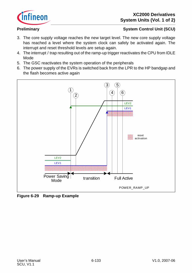
XC2000 DerivativesSystem Units (Vol. 1 of 2)
System Control Unit (SCU)Preliminary
3. The core supply voltage reaches the new target level. The new core supply voltagehas reached a level where the system clock can safely be activated again. Theinterrupt and reset threshold levels are setup again.
4. The interrupt / trap resulting out of the ramp-up trigger reactivates the CPU from IDLEMode
5. The GSC reactivates the system operation of the peripherals6. The power supply of the EVRs is switched back from the LPR to the HP bandgap and
the flash becomes active again
Figure 6-29 Ramp-up Example
2
POWER_RAMP_UP
Power SavingMode Full Activetransition
13
LEV1
LEV2
LEV2
LEV1
resetactivation
4
5
6
User’s Manual 6-133 V1.0, 2007-06SCU, V1.1

XC2000 DerivativesSystem Units (Vol. 1 of 2)
System Control Unit (SCU)Preliminary
6.5.7 Power Control Registers
6.5.7.1 PSC Status and Control Registers
SEQCONSequence Control Register
SFR (FEE4H/72H) Reset Value: 8004H
15 14 13 12 11 10 9 8 7 6 5 4 3 2 1 0
GSCBY
SEQBOSCDIS
SEQAOSCDIS
0ESR
2EN
ESR1
EN
ESR0
EN
WUTEN 0 IDLE
EN
SEQB
EN
SEQA
EN0
SEQA
TRGrw rw rw r rw rw rw rw r rw rwh rwh r w
Field Bits Type DescriptionSEQATRG 0 w Sequence A Trigger
Setting this bit trigger a power transition defined by sequence A0B No action1B Sequence A is startedSequence A is only started if Sequence B is not currently active.This bit is automatically cleared and always read as zero.
SEQAEN 2 rwh Sequence A Enable0B Sequence A is never started1B Sequence A is started if requestedSequence A is only started if Sequence B is not currently active.This bit is automatically cleared after the sequence was started.
SEQBEN 3 rwh Sequence B Enable0B Sequence B is never started1B Sequence B is started if requestedSequence B is only started if Sequence A is not currently active.This bit is automatically cleared after the sequence was started.
User’s Manual 6-134 V1.0, 2007-06SCU, V1.1
XC2000 DerivativesSystem Units (Vol. 1 of 2)
System Control Unit (SCU)Preliminary
IDLEEN 4 rw IDLE Trigger EnableThis bit defines if the IDLE instruction can trigger sequence A or not.0B Sequence A is never triggered by the IDLE
instruction1B Sequence A is triggered by the IDLE
instructionWUTEN 8 rw WUT Trigger Enable
This bit defines if an WUT event can trigger sequence B or not.0B Sequence B is never triggered by an WUT
event1B Sequence B is triggered by WUT event
ESR0EN 9 rw ESR0 Trigger EnableThis bit defines if an ESR0 event can trigger sequence B or not.0B Sequence B is never triggered by an ESR0
event1B Sequence B is triggered by ESR0 event
ESR1EN 10 rw ESR1 Trigger EnableThis bit defines if an ESR1 event can trigger sequence B or not.0B Sequence B is never triggered by an ESR1
event1B Sequence B is triggered by ESR1 event
ESR2EN 11 rw ESR2 Trigger EnableThis bit defines if an ESR2 event can trigger sequence B or not.0B Sequence B is never triggered by an ESR2
event1B Sequence B is triggered by ESR2 event
SEQAOSCEN 13 rw Sequence A OSC_WU EnableThis bit defines if the OSC_WU is enabled with the end of the sequence A.0B The enable setting for OSC_WU is left
unchanged1B OSC_WU is disabled
Field Bits Type Description
User’s Manual 6-135 V1.0, 2007-06SCU, V1.1
XC2000 DerivativesSystem Units (Vol. 1 of 2)
System Control Unit (SCU)Preliminary
SEQBOSCEN 14 rw Sequence B OSC_WU EnableThis bit defines if the OSC_WU is enabled with the end of the sequence B.0B The enable setting for OSC_WU is left
unchanged1B OSC_WU is disabled
GSCBY 15 rw GSC BypassThis bit defines if an PSC event can trigger GSC action or not.0B The normal GSC action is requested1B No GSC action is started
0 1,[7:5], 12
r ReservedRead as 0; should be written with 0.
STEP0Step 0 Register SFR (FEF2H/79H) Reset Value: C063H
15 14 13 12 11 10 9 8 7 6 5 4 3 2 1 0
1PVC
1OFF
PVCM
OFF
SYSDIV TRGSEL CLK
EN1CLKENM V1 VM
rwh rwh rwh rwh rwh rwh rwh rwh rwh
Field Bits Type DescriptionVM [2:0] rwh DMP_M Voltage Configuration
This bit defines the DMP_M core supply voltage that is requested from EVR_M.000B Full Voltage with HP bandgap selected001B Reduced Voltage with LPR selected010B Reserved, do not use this combination011B Full Voltage with LPR selected100B Off is configured101B Off is configured110B Off is configured111B Off is configured
Field Bits Type Description
User’s Manual 6-136 V1.0, 2007-06SCU, V1.1
XC2000 DerivativesSystem Units (Vol. 1 of 2)
System Control Unit (SCU)Preliminary
V1 [5:3] rwh DMP_1 Voltage ConfigurationThis bit defines the DMP_1 core supply voltage that is requested from EVR_1.000B Full Voltage with HP bandgap selected. If
DMP_1 was not powered before this is not changed and only the EVR configuration is changed.
001B Reduced Voltage with LPR selected. If DMP_1 was not powered before this is not changed and only the EVR configuration is changed.
010B Reserved, do not use this combination011B Full Voltage with LPR selected. If DMP_1 was
not powered before this is not changed and only the EVR configuration is changed.
100B Off is configured, all clocks in the DMP_1 are disabled and DMP_1 is not longer powered
101B Configuration is unchanged reading returns last configured value out of 000B, 001B, 010B, 011B, or 100B but DMP_1 is powered with EVR_1 configuration
110B Configuration is unchanged reading returns last configured value out of 000B, 001B, 010B, 011B, or 100B, all clocks in the DMP_1 are enabled
111B Configuration is unchanged reading returns last configured value out of 000B, 001B, 010B, 011B, or 100B, all clocks in the DMP_1 are disabled
CLKENM 6 rwh System Clock Enable for DMP_MThis bit defines the system clock have to be stopped for DMP_M.0B System clock for DMP_M is stopped1B System clock for DMP_M is running
CLKEN1 7 rwh System Clock Enable for DMP_1This bit defines the system clock have to be stopped for DMP_1.0B System clock for DMP_1 is stopped1B System clock for DMP_1 is running
Field Bits Type Description
User’s Manual 6-137 V1.0, 2007-06SCU, V1.1

XC2000 DerivativesSystem Units (Vol. 1 of 2)
System Control Unit (SCU)Preliminary
TRGSEL [11:8] rwh Trigger SelectionThis bit field defines the which of the four possible OK outputs from both PVCs are used for validating the power transition.0000BNon of the outputs is used0001BOK 1 from PVC_M is used0010BOK 2 from PVC_M is used0011BOK 1 from PVC_M AND OK 2 from PVC_M is
used0100BOK 1 from PVC_1 is used0101BOK 1 from PVC_M AND OK 1 from PVC_1 is
used0110BOK 2 from PVC_M AND OK 1 from PVC_1 is
used0111BOK 1 from PVC_M AND OK 2 from PVC_M
AND OK 1 from PVC_1 is used1000BOK 2 from PVC_1 is used1001BOK 1 from PVC_M AND OK 2 from PVC_1 is
used1010BOK 2 from PVC_M AND OK 2 from PVC_1 is
used1011BOK 1 from PVC_M AND OK 2 from PVC_M
AND OK 2 from PVC_1 is used1100BOK 1 from PVC_1 AND OK 2 from PVC_1 is
used1101BOK 1 from PVC_M AND OK 1 from PVC_1
AND OK 2 from PVC_1 is used1110BOK 2 from PVC_M AND OK 1 from PVC_1
AND OK2 from PVC_1 is used1111BOK 1 from PVC_M AND OK 2 from PVC_M
AND OK 1 from PVC_1 AND OK2 from PVC_1 is used
SYSDIV 12 rwh System Clock DividerThis bit defines the number of system clock cycles fSYS before the sequence is continued.0B The sequence is continued after 1 fSYS cycles1B The sequence is continued after 64 fSYS cycles
Field Bits Type Description
User’s Manual 6-138 V1.0, 2007-06SCU, V1.1
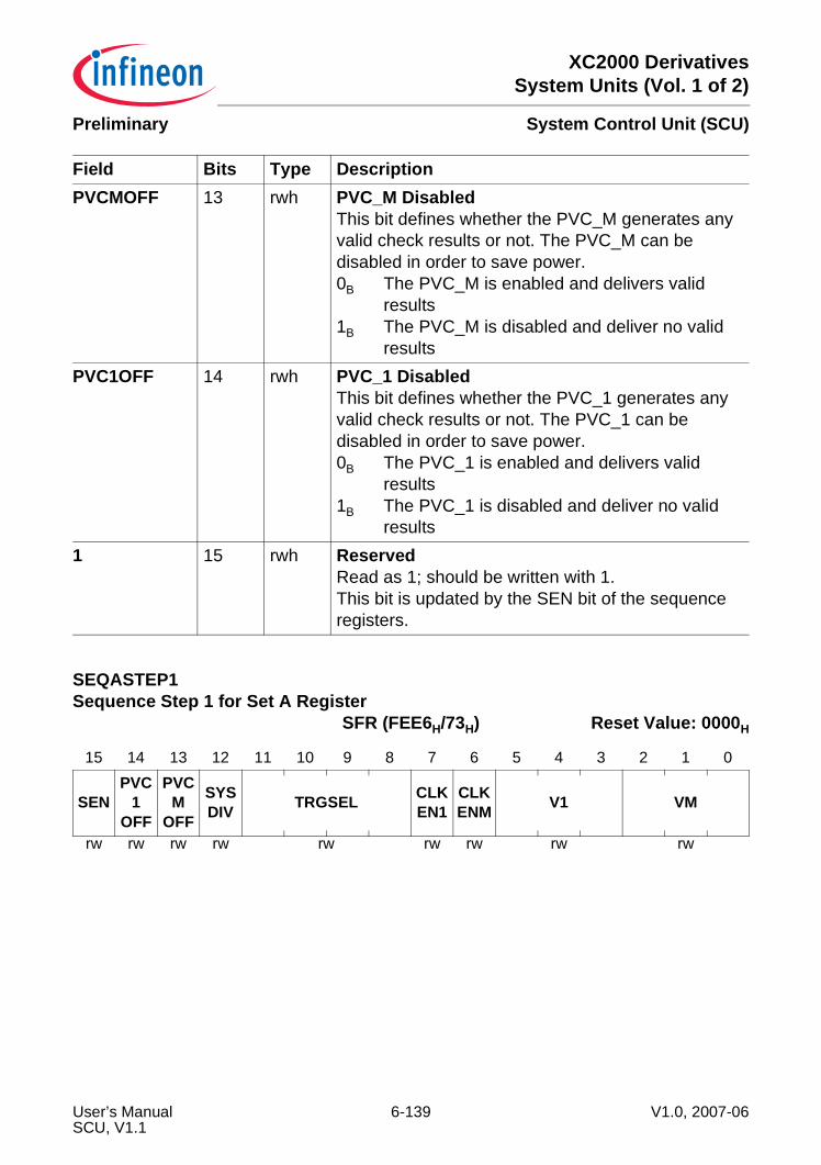
XC2000 DerivativesSystem Units (Vol. 1 of 2)
System Control Unit (SCU)Preliminary
PVCMOFF 13 rwh PVC_M DisabledThis bit defines whether the PVC_M generates any valid check results or not. The PVC_M can be disabled in order to save power.0B The PVC_M is enabled and delivers valid
results1B The PVC_M is disabled and deliver no valid
resultsPVC1OFF 14 rwh PVC_1 Disabled
This bit defines whether the PVC_1 generates any valid check results or not. The PVC_1 can be disabled in order to save power.0B The PVC_1 is enabled and delivers valid
results1B The PVC_1 is disabled and deliver no valid
results1 15 rwh Reserved
Read as 1; should be written with 1.This bit is updated by the SEN bit of the sequence registers.
SEQASTEP1Sequence Step 1 for Set A Register
SFR (FEE6H/73H) Reset Value: 0000H
15 14 13 12 11 10 9 8 7 6 5 4 3 2 1 0
SENPVC
1OFF
PVCM
OFF
SYSDIV TRGSEL CLK
EN1CLKENM V1 VM
rw rw rw rw rw rw rw rw rw
Field Bits Type Description
User’s Manual 6-139 V1.0, 2007-06SCU, V1.1
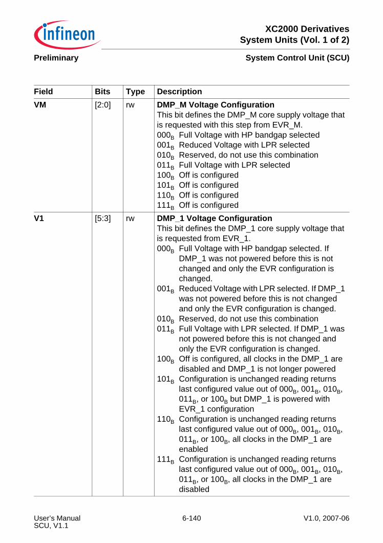
XC2000 DerivativesSystem Units (Vol. 1 of 2)
System Control Unit (SCU)Preliminary
Field Bits Type DescriptionVM [2:0] rw DMP_M Voltage Configuration
This bit defines the DMP_M core supply voltage that is requested with this step from EVR_M.000B Full Voltage with HP bandgap selected001B Reduced Voltage with LPR selected010B Reserved, do not use this combination011B Full Voltage with LPR selected100B Off is configured101B Off is configured110B Off is configured111B Off is configured
V1 [5:3] rw DMP_1 Voltage ConfigurationThis bit defines the DMP_1 core supply voltage that is requested from EVR_1.000B Full Voltage with HP bandgap selected. If
DMP_1 was not powered before this is not changed and only the EVR configuration is changed.
001B Reduced Voltage with LPR selected. If DMP_1 was not powered before this is not changed and only the EVR configuration is changed.
010B Reserved, do not use this combination011B Full Voltage with LPR selected. If DMP_1 was
not powered before this is not changed and only the EVR configuration is changed.
100B Off is configured, all clocks in the DMP_1 are disabled and DMP_1 is not longer powered
101B Configuration is unchanged reading returns last configured value out of 000B, 001B, 010B, 011B, or 100B but DMP_1 is powered with EVR_1 configuration
110B Configuration is unchanged reading returns last configured value out of 000B, 001B, 010B, 011B, or 100B, all clocks in the DMP_1 are enabled
111B Configuration is unchanged reading returns last configured value out of 000B, 001B, 010B, 011B, or 100B, all clocks in the DMP_1 are disabled
User’s Manual 6-140 V1.0, 2007-06SCU, V1.1

XC2000 DerivativesSystem Units (Vol. 1 of 2)
System Control Unit (SCU)Preliminary
CLKENM 6 rw System Clock Enable for DMP_MThis bit defines the system clock have to be stopped till the next step or not for DMP_M.0B System clock for DMP_M is stopped1B System clock for DMP_M is running
CLKEN1 7 rw System Clock Enable for DMP_1This bit defines the system clock have to be stopped till the next step or not for DMP_1.0B System clock for DMP_1 is stopped1B System clock for DMP_1 is running
Field Bits Type Description
User’s Manual 6-141 V1.0, 2007-06SCU, V1.1
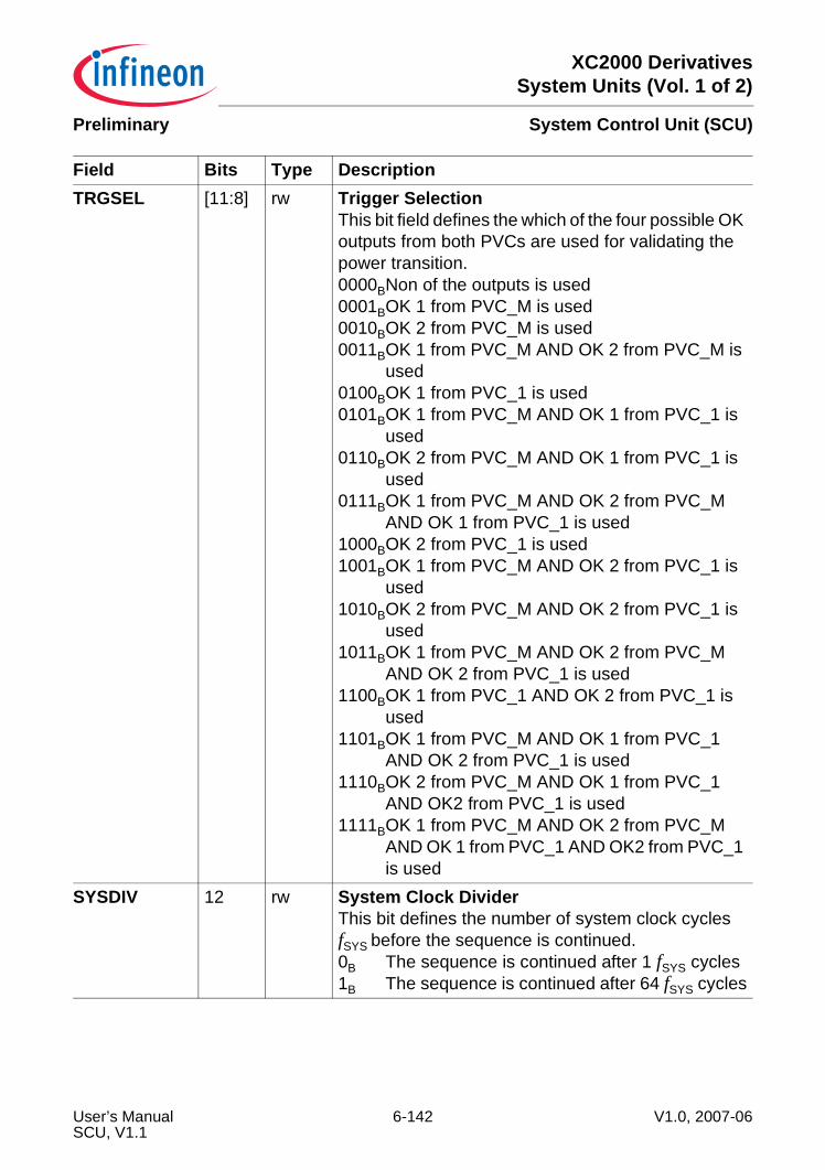
XC2000 DerivativesSystem Units (Vol. 1 of 2)
System Control Unit (SCU)Preliminary
TRGSEL [11:8] rw Trigger SelectionThis bit field defines the which of the four possible OK outputs from both PVCs are used for validating the power transition.0000BNon of the outputs is used0001BOK 1 from PVC_M is used0010BOK 2 from PVC_M is used0011BOK 1 from PVC_M AND OK 2 from PVC_M is
used0100BOK 1 from PVC_1 is used0101BOK 1 from PVC_M AND OK 1 from PVC_1 is
used0110BOK 2 from PVC_M AND OK 1 from PVC_1 is
used0111BOK 1 from PVC_M AND OK 2 from PVC_M
AND OK 1 from PVC_1 is used1000BOK 2 from PVC_1 is used1001BOK 1 from PVC_M AND OK 2 from PVC_1 is
used1010BOK 2 from PVC_M AND OK 2 from PVC_1 is
used1011BOK 1 from PVC_M AND OK 2 from PVC_M
AND OK 2 from PVC_1 is used1100BOK 1 from PVC_1 AND OK 2 from PVC_1 is
used1101BOK 1 from PVC_M AND OK 1 from PVC_1
AND OK 2 from PVC_1 is used1110BOK 2 from PVC_M AND OK 1 from PVC_1
AND OK2 from PVC_1 is used1111BOK 1 from PVC_M AND OK 2 from PVC_M
AND OK 1 from PVC_1 AND OK2 from PVC_1 is used
SYSDIV 12 rw System Clock DividerThis bit defines the number of system clock cycles fSYS before the sequence is continued.0B The sequence is continued after 1 fSYS cycles1B The sequence is continued after 64 fSYS cycles
Field Bits Type Description
User’s Manual 6-142 V1.0, 2007-06SCU, V1.1

XC2000 DerivativesSystem Units (Vol. 1 of 2)
System Control Unit (SCU)Preliminary
PVCMOFF 13 rw PVC_M DisabledThis bit defines whether the PVC generates any valid check results or not for this step. The PVC can be disabled in order to save power.0B The PVC_M is enabled and delivers valid
results1B The PVC_M is disabled and deliver no valid
resultsPVC1OFF 14 rw PVC_1 Disabled
This bit defines whether the PVC generates any valid check results or not for this step. The PVC can be disabled in order to save power.0B The PVC_1 is enabled and delivers valid
results1B The PVC_1 is disabled and deliver no valid
resultsSEN 15 rw Step Enable
This bit defines the operation that is connected with step n of the transition is skipped or not.0B Step is skipped1B Step is executed
Field Bits Type Description
User’s Manual 6-143 V1.0, 2007-06SCU, V1.1
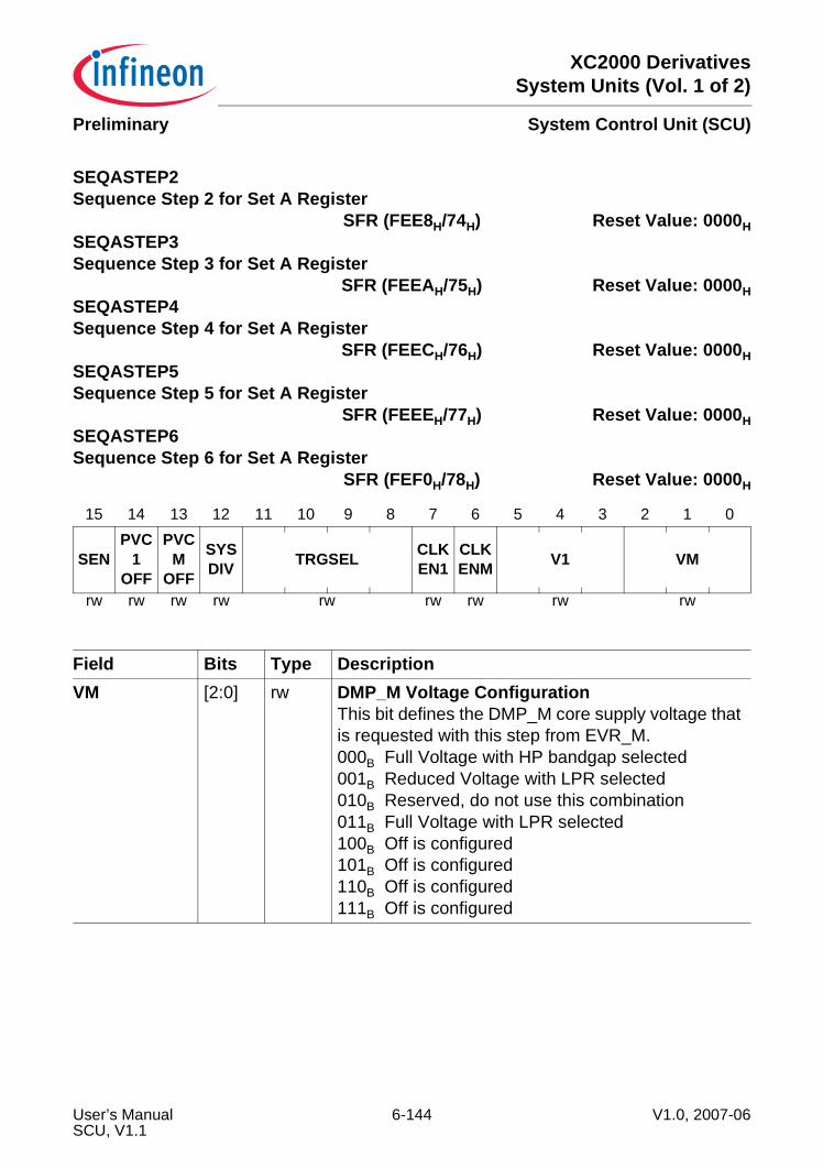
XC2000 DerivativesSystem Units (Vol. 1 of 2)
System Control Unit (SCU)Preliminary
SEQASTEP2Sequence Step 2 for Set A Register
SFR (FEE8H/74H) Reset Value: 0000HSEQASTEP3Sequence Step 3 for Set A Register
SFR (FEEAH/75H) Reset Value: 0000HSEQASTEP4Sequence Step 4 for Set A Register
SFR (FEECH/76H) Reset Value: 0000HSEQASTEP5Sequence Step 5 for Set A Register
SFR (FEEEH/77H) Reset Value: 0000HSEQASTEP6Sequence Step 6 for Set A Register
SFR (FEF0H/78H) Reset Value: 0000H
15 14 13 12 11 10 9 8 7 6 5 4 3 2 1 0
SENPVC
1OFF
PVCM
OFF
SYSDIV TRGSEL CLK
EN1CLKENM V1 VM
rw rw rw rw rw rw rw rw rw
Field Bits Type DescriptionVM [2:0] rw DMP_M Voltage Configuration
This bit defines the DMP_M core supply voltage that is requested with this step from EVR_M.000B Full Voltage with HP bandgap selected001B Reduced Voltage with LPR selected010B Reserved, do not use this combination011B Full Voltage with LPR selected100B Off is configured101B Off is configured110B Off is configured111B Off is configured
User’s Manual 6-144 V1.0, 2007-06SCU, V1.1
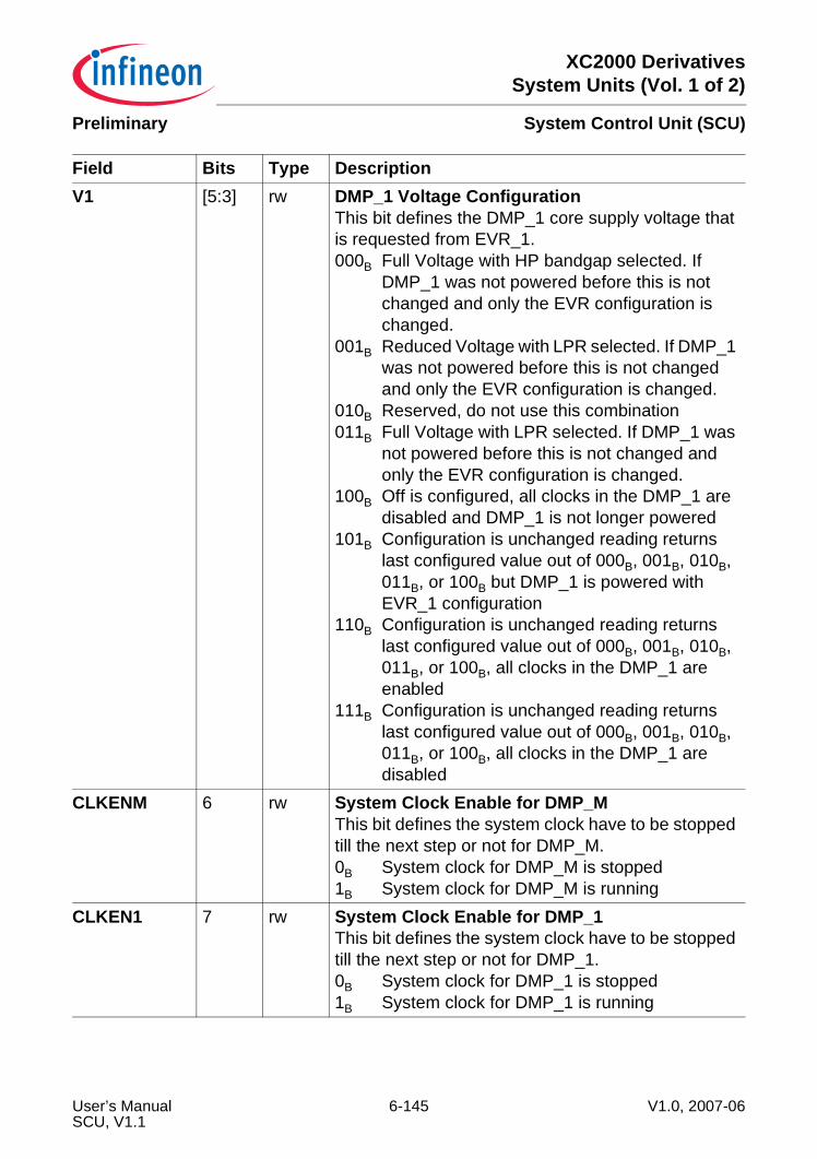
XC2000 DerivativesSystem Units (Vol. 1 of 2)
System Control Unit (SCU)Preliminary
V1 [5:3] rw DMP_1 Voltage ConfigurationThis bit defines the DMP_1 core supply voltage that is requested from EVR_1.000B Full Voltage with HP bandgap selected. If
DMP_1 was not powered before this is not changed and only the EVR configuration is changed.
001B Reduced Voltage with LPR selected. If DMP_1 was not powered before this is not changed and only the EVR configuration is changed.
010B Reserved, do not use this combination011B Full Voltage with LPR selected. If DMP_1 was
not powered before this is not changed and only the EVR configuration is changed.
100B Off is configured, all clocks in the DMP_1 are disabled and DMP_1 is not longer powered
101B Configuration is unchanged reading returns last configured value out of 000B, 001B, 010B, 011B, or 100B but DMP_1 is powered with EVR_1 configuration
110B Configuration is unchanged reading returns last configured value out of 000B, 001B, 010B, 011B, or 100B, all clocks in the DMP_1 are enabled
111B Configuration is unchanged reading returns last configured value out of 000B, 001B, 010B, 011B, or 100B, all clocks in the DMP_1 are disabled
CLKENM 6 rw System Clock Enable for DMP_MThis bit defines the system clock have to be stopped till the next step or not for DMP_M.0B System clock for DMP_M is stopped1B System clock for DMP_M is running
CLKEN1 7 rw System Clock Enable for DMP_1This bit defines the system clock have to be stopped till the next step or not for DMP_1.0B System clock for DMP_1 is stopped1B System clock for DMP_1 is running
Field Bits Type Description
User’s Manual 6-145 V1.0, 2007-06SCU, V1.1
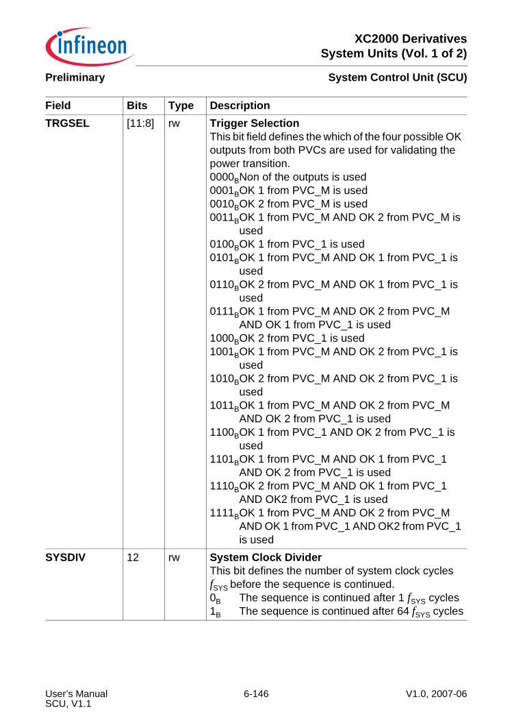
XC2000 DerivativesSystem Units (Vol. 1 of 2)
System Control Unit (SCU)Preliminary
TRGSEL [11:8] rw Trigger SelectionThis bit field defines the which of the four possible OK outputs from both PVCs are used for validating the power transition.0000BNon of the outputs is used0001BOK 1 from PVC_M is used0010BOK 2 from PVC_M is used0011BOK 1 from PVC_M AND OK 2 from PVC_M is
used0100BOK 1 from PVC_1 is used0101BOK 1 from PVC_M AND OK 1 from PVC_1 is
used0110BOK 2 from PVC_M AND OK 1 from PVC_1 is
used0111BOK 1 from PVC_M AND OK 2 from PVC_M
AND OK 1 from PVC_1 is used1000BOK 2 from PVC_1 is used1001BOK 1 from PVC_M AND OK 2 from PVC_1 is
used1010BOK 2 from PVC_M AND OK 2 from PVC_1 is
used1011BOK 1 from PVC_M AND OK 2 from PVC_M
AND OK 2 from PVC_1 is used1100BOK 1 from PVC_1 AND OK 2 from PVC_1 is
used1101BOK 1 from PVC_M AND OK 1 from PVC_1
AND OK 2 from PVC_1 is used1110BOK 2 from PVC_M AND OK 1 from PVC_1
AND OK2 from PVC_1 is used1111BOK 1 from PVC_M AND OK 2 from PVC_M
AND OK 1 from PVC_1 AND OK2 from PVC_1 is used
SYSDIV 12 rw System Clock DividerThis bit defines the number of system clock cycles fSYS before the sequence is continued.0B The sequence is continued after 1 fSYS cycles1B The sequence is continued after 64 fSYS cycles
Field Bits Type Description
User’s Manual 6-146 V1.0, 2007-06SCU, V1.1
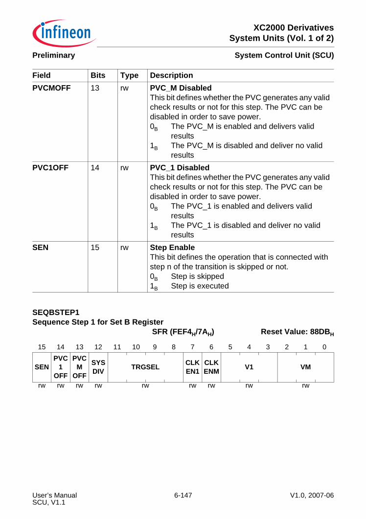
XC2000 DerivativesSystem Units (Vol. 1 of 2)
System Control Unit (SCU)Preliminary
PVCMOFF 13 rw PVC_M DisabledThis bit defines whether the PVC generates any valid check results or not for this step. The PVC can be disabled in order to save power.0B The PVC_M is enabled and delivers valid
results1B The PVC_M is disabled and deliver no valid
resultsPVC1OFF 14 rw PVC_1 Disabled
This bit defines whether the PVC generates any valid check results or not for this step. The PVC can be disabled in order to save power.0B The PVC_1 is enabled and delivers valid
results1B The PVC_1 is disabled and deliver no valid
resultsSEN 15 rw Step Enable
This bit defines the operation that is connected with step n of the transition is skipped or not.0B Step is skipped1B Step is executed
SEQBSTEP1Sequence Step 1 for Set B Register
SFR (FEF4H/7AH) Reset Value: 88DBH
15 14 13 12 11 10 9 8 7 6 5 4 3 2 1 0
SENPVC
1OFF
PVCM
OFF
SYSDIV TRGSEL CLK
EN1CLKENM V1 VM
rw rw rw rw rw rw rw rw rw
Field Bits Type Description
User’s Manual 6-147 V1.0, 2007-06SCU, V1.1

XC2000 DerivativesSystem Units (Vol. 1 of 2)
System Control Unit (SCU)Preliminary
Field Bits Type DescriptionVM [2:0] rw DMP_M Voltage Configuration
This bit defines the DMP_M core supply voltage that is requested with this step from EVR_M.000B Full Voltage with HP bandgap selected001B Reduced Voltage with LPR selected010B Reserved, do not use this combination011B Full Voltage with LPR selected100B Off is configured101B Off is configured110B Off is configured111B Off is configured
V1 [5:3] rw DMP_1 Voltage ConfigurationThis bit defines the DMP_1 core supply voltage that is requested from EVR_1.000B Full Voltage with HP bandgap selected. If
DMP_1 was not powered before this is not changed and only the EVR configuration is changed.
001B Reduced Voltage with LPR selected. If DMP_1 was not powered before this is not changed and only the EVR configuration is changed.
010B Reserved, do not use this combination011B Full Voltage with LPR selected. If DMP_1 was
not powered before this is not changed and only the EVR configuration is changed.
100B Off is configured, all clocks in the DMP_1 are disabled and DMP_1 is not longer powered
101B Configuration is unchanged reading returns last configured value out of 000B, 001B, 010B, 011B, or 100B but DMP_1 is powered with EVR_1 configuration
110B Configuration is unchanged reading returns last configured value out of 000B, 001B, 010B, 011B, or 100B, all clocks in the DMP_1 are enabled
111B Configuration is unchanged reading returns last configured value out of 000B, 001B, 010B, 011B, or 100B, all clocks in the DMP_1 are disabled
User’s Manual 6-148 V1.0, 2007-06SCU, V1.1
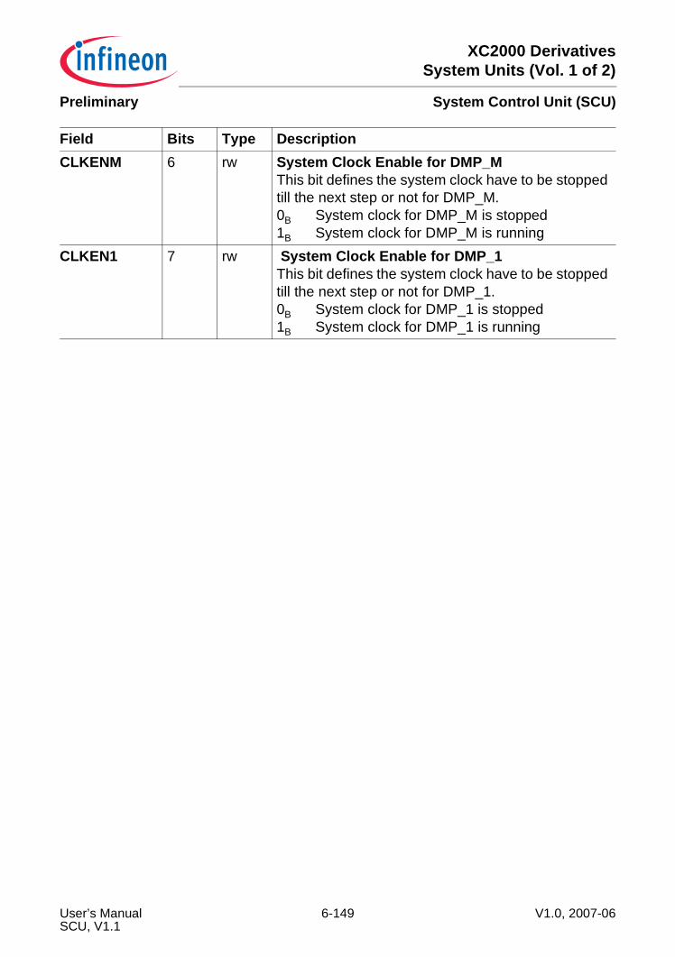
XC2000 DerivativesSystem Units (Vol. 1 of 2)
System Control Unit (SCU)Preliminary
CLKENM 6 rw System Clock Enable for DMP_MThis bit defines the system clock have to be stopped till the next step or not for DMP_M.0B System clock for DMP_M is stopped1B System clock for DMP_M is running
CLKEN1 7 rw System Clock Enable for DMP_1This bit defines the system clock have to be stopped till the next step or not for DMP_1.0B System clock for DMP_1 is stopped1B System clock for DMP_1 is running
Field Bits Type Description
User’s Manual 6-149 V1.0, 2007-06SCU, V1.1

XC2000 DerivativesSystem Units (Vol. 1 of 2)
System Control Unit (SCU)Preliminary
TRGSEL [11:8] rw Trigger SelectionThis bit field defines the which of the four possible OK outputs from both PVCs are used for validating the power transition.0000BNon of the outputs is used0001BOK 1 from PVC_M is used0010BOK 2 from PVC_M is used0011BOK 1 from PVC_M AND OK 2 from PVC_M is
used0100BOK 1 from PVC_1 is used0101BOK 1 from PVC_M AND OK 1 from PVC_1 is
used0110BOK 2 from PVC_M AND OK 1 from PVC_1 is
used0111BOK 1 from PVC_M AND OK 2 from PVC_M
AND OK 1 from PVC_1 is used1000BOK 2 from PVC_1 is used1001BOK 1 from PVC_M AND OK 2 from PVC_1 is
used1010BOK 2 from PVC_M AND OK 2 from PVC_1 is
used1011BOK 1 from PVC_M AND OK 2 from PVC_M
AND OK 2 from PVC_1 is used1100BOK 1 from PVC_1 AND OK 2 from PVC_1 is
used1101BOK 1 from PVC_M AND OK 1 from PVC_1
AND OK 2 from PVC_1 is used1110BOK 2 from PVC_M AND OK 1 from PVC_1
AND OK2 from PVC_1 is used1111BOK 1 from PVC_M AND OK 2 from PVC_M
AND OK 1 from PVC_1 AND OK2 from PVC_1 is used
SYSDIV 12 rw System Clock DividerThis bit defines the number of system clock cycles fSYS before the sequence is continued.0B The sequence is continued after 1 fSYS cycles1B The sequence is continued after 64 fSYS cycles
Field Bits Type Description
User’s Manual 6-150 V1.0, 2007-06SCU, V1.1
XC2000 DerivativesSystem Units (Vol. 1 of 2)
System Control Unit (SCU)Preliminary
PVCMOFF 13 rw PVC_M DisabledThis bit defines whether the PVC generates any valid check results or not for this step. The PVC can be disabled in order to save power.0B The PVC_M is enabled and delivers valid
results1B The PVC_M is disabled and deliver no valid
resultsPVC1OFF 14 rw PVC_1 Disabled
This bit defines whether the PVC generates any valid check results or not for this step. The PVC can be disabled in order to save power.0B The PVC_1 is enabled and delivers valid
results1B The PVC_1 is disabled and deliver no valid
resultsSEN 15 rw Step Enable
This bit defines the operation that is connected with step n of the transition is skipped or not.0B Step is skipped1B Step is executed
Field Bits Type Description
User’s Manual 6-151 V1.0, 2007-06SCU, V1.1

XC2000 DerivativesSystem Units (Vol. 1 of 2)
System Control Unit (SCU)Preliminary
SEQBSTEP2Sequence Step 2 for Set B Register
SFR (FEF6H/7BH) Reset Value: 80EBHSEQBSTEP3Sequence Step 3 for Set B Register
SFR (FEF8H/7CH) Reset Value: 80F3HSEQBSTEP4Sequence Step 4 for Set B Register
SFR (FEFAH/7DH) Reset Value: 0000HSEQBSTEP5Sequence Step 5 for Set B Register
SFR (FEFCH/7EH) Reset Value: 0000HSEQBSTEP6Sequence Step 6 for Set B Register
SFR (FEFEH/7FH) Reset Value: 0000H
15 14 13 12 11 10 9 8 7 6 5 4 3 2 1 0
SENPVC
1OFF
PVCM
OFF
SYSDIV TRGSEL CLK
EN1CLKENM V1 VM
rw rw rw rw rw rw rw rw rw
Field Bits Type DescriptionVM [2:0] rw DMP_M Voltage Configuration
This bit defines the DMP_M core supply voltage that is requested with this step from EVR_M.000B Full Voltage with HP bandgap selected001B Reduced Voltage with LPR selected010B Reserved, do not use this combination011B Full Voltage with LPR selected100B Off is configured101B Off is configured110B Off is configured111B Off is configured
User’s Manual 6-152 V1.0, 2007-06SCU, V1.1

XC2000 DerivativesSystem Units (Vol. 1 of 2)
System Control Unit (SCU)Preliminary
V1 [5:3] rw DMP_1 Voltage ConfigurationThis bit defines the DMP_1 core supply voltage that is requested from EVR_1.000B Full Voltage with HP bandgap selected. If
DMP_1 was not powered before this is not changed and only the EVR configuration is changed.
001B Reduced Voltage with LPR selected. If DMP_1 was not powered before this is not changed and only the EVR configuration is changed.
010B Reserved, do not use this combination011B Full Voltage with LPR selected. If DMP_1 was
not powered before this is not changed and only the EVR configuration is changed.
100B Off is configured, all clocks in the DMP_1 are disabled and DMP_1 is not longer powered
101B Configuration is unchanged reading returns last configured value out of 000B, 001B, 010B, 011B, or 100B but DMP_1 is powered with EVR_1 configuration
110B Configuration is unchanged reading returns last configured value out of 000B, 001B, 010B, 011B, or 100B, all clocks in the DMP_1 are enabled
111B Configuration is unchanged reading returns last configured value out of 000B, 001B, 010B, 011B, or 100B, all clocks in the DMP_1 are disabled
CLKENM 6 rw System Clock Enable for DMP_MThis bit defines the system clock have to be stopped till the next step or not for DMP_M.0B System clock for DMP_M is stopped1B System clock for DMP_M is running
CLKEN1 7 rw System Clock Enable for DMP_1This bit defines the system clock have to be stopped till the next step or not for DMP_1.0B System clock for DMP_1 is stopped1B System clock for DMP_1 is running
Field Bits Type Description
User’s Manual 6-153 V1.0, 2007-06SCU, V1.1

XC2000 DerivativesSystem Units (Vol. 1 of 2)
System Control Unit (SCU)Preliminary
TRGSEL [11:8] rw Trigger SelectionThis bit field defines the which of the four possible OK outputs from both PVCs are used for validating the power transition.0000BNon of the outputs is used0001BOK 1 from PVC_M is used0010BOK 2 from PVC_M is used0011BOK 1 from PVC_M AND OK 2 from PVC_M is
used0100BOK 1 from PVC_1 is used0101BOK 1 from PVC_M AND OK 1 from PVC_1 is
used0110BOK 2 from PVC_M AND OK 1 from PVC_1 is
used0111BOK 1 from PVC_M AND OK 2 from PVC_M
AND OK 1 from PVC_1 is used1000BOK 2 from PVC_1 is used1001BOK 1 from PVC_M AND OK 2 from PVC_1 is
used1010BOK 2 from PVC_M AND OK 2 from PVC_1 is
used1011BOK 1 from PVC_M AND OK 2 from PVC_M
AND OK 2 from PVC_1 is used1100BOK 1 from PVC_1 AND OK 2 from PVC_1 is
used1101BOK 1 from PVC_M AND OK 1 from PVC_1
AND OK 2 from PVC_1 is used1110BOK 2 from PVC_M AND OK 1 from PVC_1
AND OK2 from PVC_1 is used1111BOK 1 from PVC_M AND OK 2 from PVC_M
AND OK 1 from PVC_1 AND OK2 from PVC_1 is used
SYSDIV 12 rw System Clock DividerThis bit defines the number of system clock cycles fSYS before the sequence is continued.0B The sequence is continued after 1 fSYS cycles1B The sequence is continued after 64 fSYS cycles
Field Bits Type Description
User’s Manual 6-154 V1.0, 2007-06SCU, V1.1

XC2000 DerivativesSystem Units (Vol. 1 of 2)
System Control Unit (SCU)Preliminary
PVCMOFF 13 rw PVC_M DisabledThis bit defines whether the PVC generates any valid check results or not for this step. The PVC can be disabled in order to save power.0B The PVC_M is enabled and delivers valid
results1B The PVC_M is disabled and deliver no valid
resultsPVC1OFF 14 rw PVC_1 Disabled
This bit defines whether the PVC generates any valid check results or not for this step. The PVC can be disabled in order to save power.0B The PVC_1 is enabled and delivers valid
results1B The PVC_1 is disabled and deliver no valid
resultsSEN 15 rw Step Enable
This bit defines the operation that is connected with step n of the transition is skipped or not.0B Step is skipped1B Step is executed
Field Bits Type Description
User’s Manual 6-155 V1.0, 2007-06SCU, V1.1
XC2000 DerivativesSystem Units (Vol. 1 of 2)
System Control Unit (SCU)Preliminary
6.6 Global State Controller (GSC)Beside power saving modes and the clock management Mode Control for the systemperipherals provides an additional opportunity for configuring the system to theapplication needs.Mode Control is described in detail in this chapter and is implemented by the GSC.The GSC enables the user to configure one operating mode in a fast and easy way,reacting fast and explicit to needs of an application.
Feature OverviewThe following issues are handled by the GSC:• Control of peripheral clock operation• Suspend control for debugging• Arbitration between the different request sourcesAccording to the requests coming from the OCDS, the SWD pre-warning detection orother blocks, the GSC does an internal prioritization. The result is forwarded asbroadcast command request to all peripherals. The GSC internal prioritization schemefor the implemented request sources is shown in Table 6-15.
6.6.1 GSC Control FlowAt least one request source asserts its request trigger in order to request a mode changein the SoC. If several requests are pending there is an arbitration mechanism that treatsthis issue. Request triggers are not stored by the GSC, therefore a trigger source has toassert its trigger until the trigger is no longer valid or needed.A request trigger is kept asserted as long as either the request is still pending or theresulting command of the request was entered and acknowledged by the system. Thecommunication of the GSC and the peripherals is based on commands. Three differentcommands are defined resulting in three modes:• Wake-up command
– This command defines the Normal Mode• Clock-off command
– This command defines the Stop Mode• Debug command
– This command defines the Suspend ModeEach peripheral defines its specific behavior for these three modes via the moduleregister mod_KSCCFG.
6.6.1.1 Request Source ArbitrationThe arbitration is a priority driven arbitration. The highest priority in this arbitration iszero.
User’s Manual 6-156 V1.0, 2007-06SCU, V1.1
XC2000 DerivativesSystem Units (Vol. 1 of 2)
System Control Unit (SCU)Preliminary
Each cycle a new arbitration round is started. The winner of an arbitration round canissue the next command towards the SoC. Please note that winning an arbitration doesnot lead automatically to a new command raised. Only if currently no command isbroadcast in the SoC a new command can be generated and broadcast. If the winner ofthe arbitration round is the same request trigger as in the previous round or if no winnerwas detected no new command request is generated.
6.6.1.2 Generation of a New CommandWhen a new request trigger was detected and arbitrated a new command request isgenerated if one of the following conditions is valid:• Currently no command request is broadcast that is not received by all slaves
Table 6-15 Connection of the Request SourcesRequest Source PriorityPSCB exit 0PSCB entry 1PSCA exit 2PSCA entry 3OCDS exit 4ESR0 5ESR1 6ESR2 7WUT 8ITC 9SW1 11SW2 12OCDS entry 14
Table 6-16 Request Source and Command Request CouplingRequest Source Command DescriptionPSCB exit Wake-up; Normal ModePSCB entry Clock-off ModePSCA exit Wake-up; Normal ModePSCA entry Clock-off ModeOCDS exit Wake-up; Normal Mode
User’s Manual 6-157 V1.0, 2007-06SCU, V1.1
XC2000 DerivativesSystem Units (Vol. 1 of 2)
System Control Unit (SCU)Preliminary
6.6.1.3 Usage of CommandsThe complete control mechanism for the different operation modes of the various slavesare divided into two parts:• A central control and configuration part; the Global State Controller (GSC)• One local control part in each slave; the Kernel State Controller (KSC)Via the GSC either different hardware sources (e.g. the WUT or the OCDS) or thesoftware can request the system to enter a specific mode. The parts that are affected bythe mode can be pre-defined locally for each part via the KSC. For each command aspecific reaction can be pre-configured in each KSC for each individual part.
6.6.1.4 Terminating a Request TriggerA request trigger is no longer taken into account for the arbitration after the de-assertingof the request trigger.
6.6.1.5 Suspend Control FlowThe suspend feature is controlled by the OCDS block. The GSC operates only as controland communication interface towards the system. The suspend feature is composed outof two requirements:The mode that has to be entered when the Suspend Mode is requested.The mode that has to be entered when the Suspend Mode is left.The request to enter Suspend Mode is forwarded form the OCDS. When the SuspendMode is requested the system is expected to be stopped as soon as possible in an idlestate where no internal process is pending and in a way that this system state does notlead to any damage internally or externally and can also be left without any damage.Therefore all peripherals in the system are requested to enter a mode where the clockcan be stopped. This is done by sending a debug command.
ESR0 Wake-up; Normal ModeESR1 Wake-up; Normal ModeESR2 Clock-off ModeWUT Wake-up; Normal ModeITC Wake-up; Normal ModeSW1 Wake-up; Normal ModeSW2 Clock-off ModeOCDS entry Suspend Mode
Table 6-16 Request Source and Command Request CouplingRequest Source Command Description
User’s Manual 6-158 V1.0, 2007-06SCU, V1.1
XC2000 DerivativesSystem Units (Vol. 1 of 2)
System Control Unit (SCU)Preliminary
Leaving the Suspend Mode should serve the goal that debugging is a non-intrusiveoperation. Therefore leaving the Suspend Mode can not lead to only one dedicatedsystem mode, instead it leads to the system mode the system left when it was requestedto exit the Suspend Mode. The system mode is stored when a Suspend Mode requestis detected by the GSC and is used as target system mode when a leave Suspend Modetrigger is detected by the GSC.
6.6.1.6 Error Feedback for a Mode TransitionIn case at least one peripheral reports an error the error flag in register GSCSTAT is set.If no error is currently detected upon a new assertion of a system mode by the GSC theerror flag is cleared. To inform the system of this erroneous state an interrupt can begenerated.
User’s Manual 6-159 V1.0, 2007-06SCU, V1.1
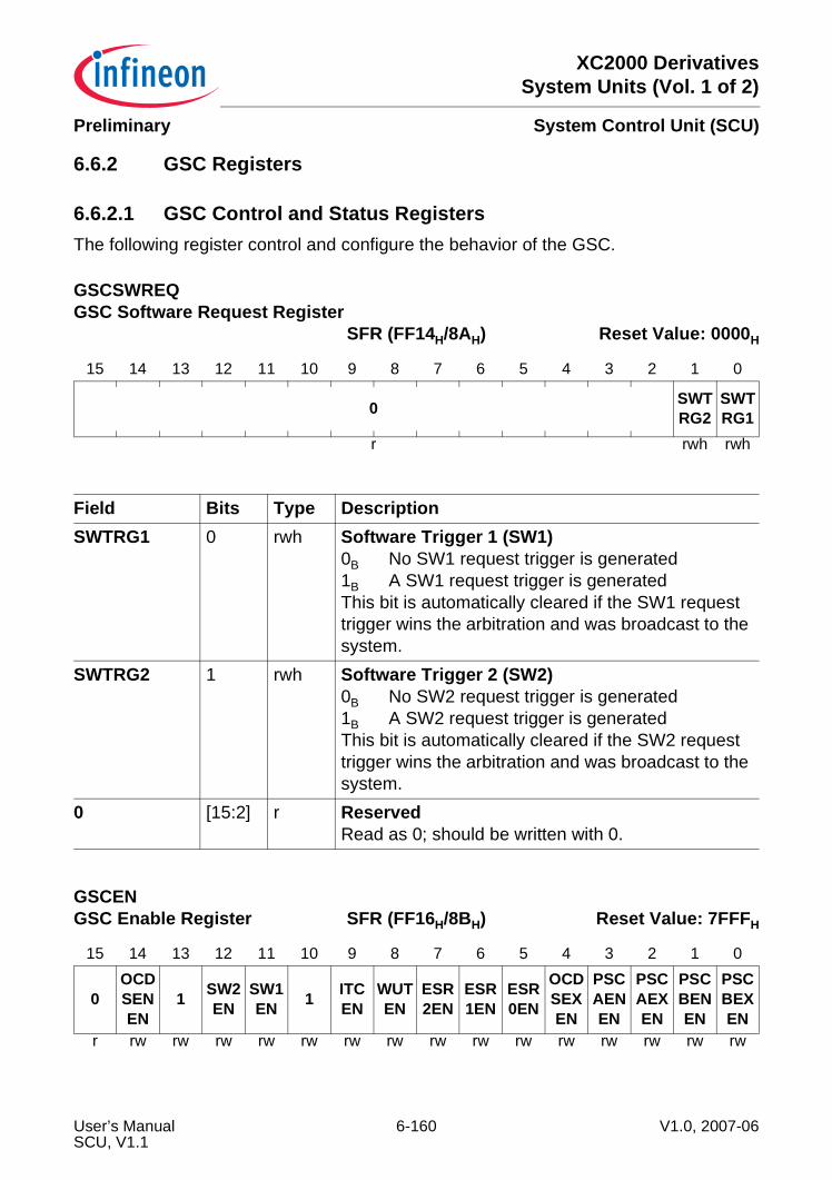
XC2000 DerivativesSystem Units (Vol. 1 of 2)
System Control Unit (SCU)Preliminary
6.6.2 GSC Registers
6.6.2.1 GSC Control and Status RegistersThe following register control and configure the behavior of the GSC.
GSCSWREQGSC Software Request Register
SFR (FF14H/8AH) Reset Value: 0000H
15 14 13 12 11 10 9 8 7 6 5 4 3 2 1 0
0 SWTRG2
SWTRG1
r rwh rwh
Field Bits Type DescriptionSWTRG1 0 rwh Software Trigger 1 (SW1)
0B No SW1 request trigger is generated1B A SW1 request trigger is generatedThis bit is automatically cleared if the SW1 request trigger wins the arbitration and was broadcast to the system.
SWTRG2 1 rwh Software Trigger 2 (SW2)0B No SW2 request trigger is generated1B A SW2 request trigger is generatedThis bit is automatically cleared if the SW2 request trigger wins the arbitration and was broadcast to the system.
0 [15:2] r ReservedRead as 0; should be written with 0.
GSCENGSC Enable Register SFR (FF16H/8BH) Reset Value: 7FFFH
15 14 13 12 11 10 9 8 7 6 5 4 3 2 1 0
0OCDSENEN
1 SW2EN
SW1EN 1 ITC
ENWUTEN
ESR2EN
ESR1EN
ESR0EN
OCDSEXEN
PSCAENEN
PSCAEXEN
PSCBENEN
PSCBEXEN
r rw rw rw rw rw rw rw rw rw rw rw rw rw rw rw
User’s Manual 6-160 V1.0, 2007-06SCU, V1.1
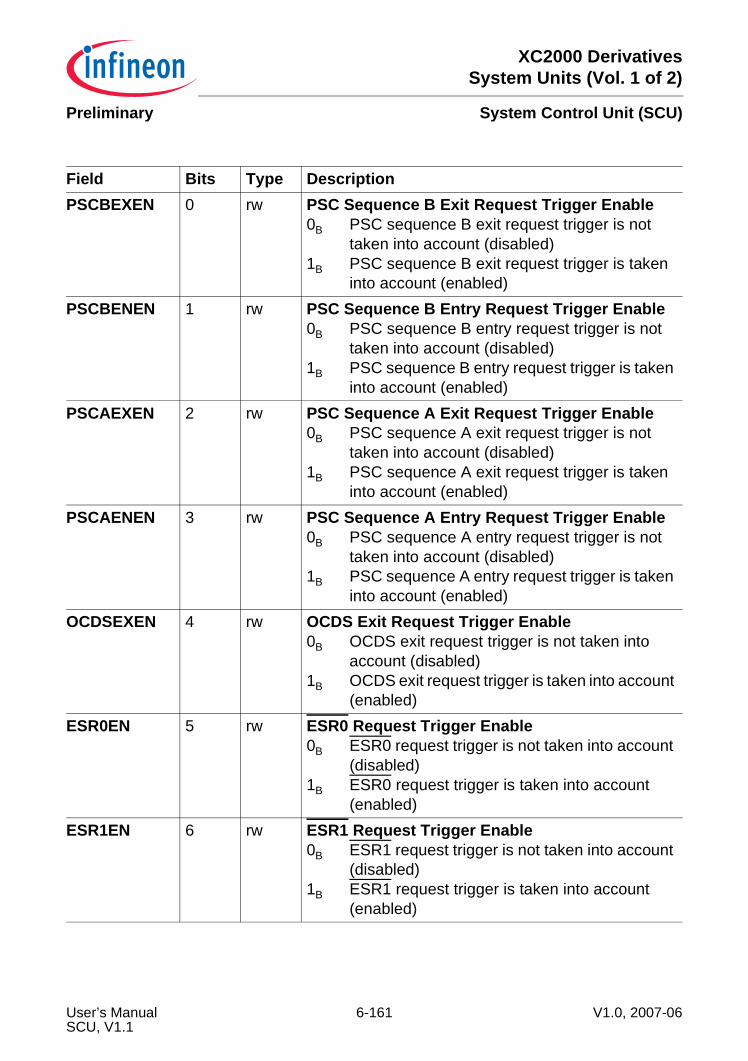
XC2000 DerivativesSystem Units (Vol. 1 of 2)
System Control Unit (SCU)Preliminary
Field Bits Type DescriptionPSCBEXEN 0 rw PSC Sequence B Exit Request Trigger Enable
0B PSC sequence B exit request trigger is not taken into account (disabled)
1B PSC sequence B exit request trigger is taken into account (enabled)
PSCBENEN 1 rw PSC Sequence B Entry Request Trigger Enable0B PSC sequence B entry request trigger is not
taken into account (disabled)1B PSC sequence B entry request trigger is taken
into account (enabled)PSCAEXEN 2 rw PSC Sequence A Exit Request Trigger Enable
0B PSC sequence A exit request trigger is not taken into account (disabled)
1B PSC sequence A exit request trigger is taken into account (enabled)
PSCAENEN 3 rw PSC Sequence A Entry Request Trigger Enable0B PSC sequence A entry request trigger is not
taken into account (disabled)1B PSC sequence A entry request trigger is taken
into account (enabled)OCDSEXEN 4 rw OCDS Exit Request Trigger Enable
0B OCDS exit request trigger is not taken into account (disabled)
1B OCDS exit request trigger is taken into account (enabled)
ESR0EN 5 rw ESR0 Request Trigger Enable0B ESR0 request trigger is not taken into account
(disabled)1B ESR0 request trigger is taken into account
(enabled)ESR1EN 6 rw ESR1 Request Trigger Enable
0B ESR1 request trigger is not taken into account (disabled)
1B ESR1 request trigger is taken into account (enabled)
User’s Manual 6-161 V1.0, 2007-06SCU, V1.1

XC2000 DerivativesSystem Units (Vol. 1 of 2)
System Control Unit (SCU)Preliminary
ESR2EN 7 rw ESR2 Request Trigger Enable0B ESR2 request trigger is not taken into account
(disabled)1B ESR2 request trigger is taken into account
(enabled)WUTEN 8 rw WUT Request Trigger Enable
0B WUT request trigger is not taken into account (disabled)
1B WUT request trigger is taken into account (enabled)
ITCEN 9 rw ITC Request Trigger Enable0B ITC request trigger is not taken into account
(disabled)1B ITC request trigger is taken into account
(enabled)SW1EN 11 rw Software 1 Request Trigger Enable
0B SW1 request trigger is not taken into account (disabled)
1B SW1 request trigger is taken into account (enabled)
SW2EN 12 rw Software 2 Request Trigger Enable0B SW2 request trigger is not taken into account
(disabled)1B SW2 request trigger is taken into account
(enabled)OCDSENEN 14 rw OCDS Entry Request Trigger Enable
0B OCDS entry request trigger is not taken into account (disabled)
1B OCDS entry request trigger is taken into account (enabled)
OCDS entry is the request source belonging to the according connector interface.
1 10, 13 rw ReservedShould be written with.
0 15 r ReservedRead as 0; should be written with 0.
Field Bits Type Description
User’s Manual 6-162 V1.0, 2007-06SCU, V1.1
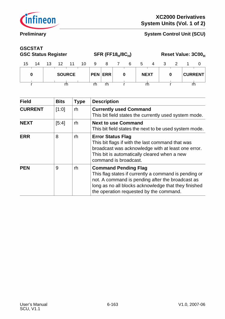
XC2000 DerivativesSystem Units (Vol. 1 of 2)
System Control Unit (SCU)Preliminary
GSCSTATGSC Status Register SFR (FF18H/8CH) Reset Value: 3C00H
15 14 13 12 11 10 9 8 7 6 5 4 3 2 1 0
0 SOURCE PEN ERR 0 NEXT 0 CURRENT
r rh rh rh r rh r rh
Field Bits Type DescriptionCURRENT [1:0] rh Currently used Command
This bit field states the currently used system mode.NEXT [5:4] rh Next to use Command
This bit field states the next to be used system mode.ERR 8 rh Error Status Flag
This bit flags if with the last command that was broadcast was acknowledge with at least one error. This bit is automatically cleared when a new command is broadcast.
PEN 9 rh Command Pending FlagThis flag states if currently a command is pending or not. A command is pending after the broadcast as long as no all blocks acknowledge that they finished the operation requested by the command.
User’s Manual 6-163 V1.0, 2007-06SCU, V1.1
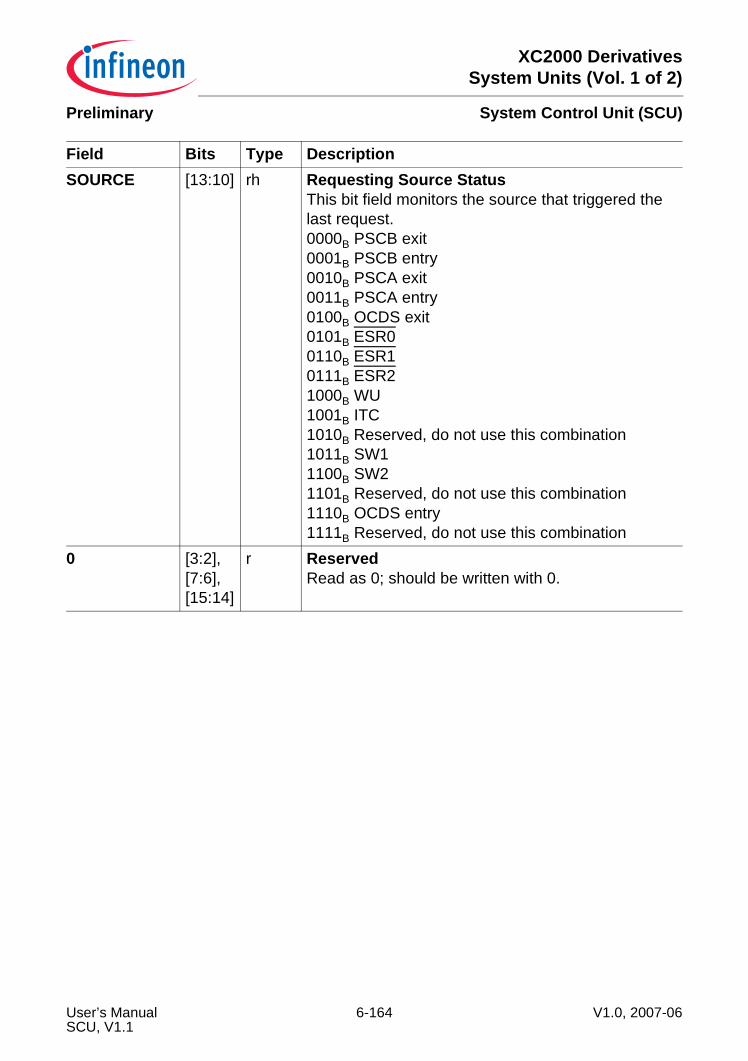
XC2000 DerivativesSystem Units (Vol. 1 of 2)
System Control Unit (SCU)Preliminary
SOURCE [13:10] rh Requesting Source StatusThis bit field monitors the source that triggered the last request.0000B PSCB exit0001B PSCB entry0010B PSCA exit0011B PSCA entry0100B OCDS exit0101B ESR00110B ESR10111B ESR21000B WU1001B ITC1010B Reserved, do not use this combination1011B SW11100B SW21101B Reserved, do not use this combination1110B OCDS entry1111B Reserved, do not use this combination
0 [3:2],[7:6],[15:14]
r ReservedRead as 0; should be written with 0.
Field Bits Type Description
User’s Manual 6-164 V1.0, 2007-06SCU, V1.1
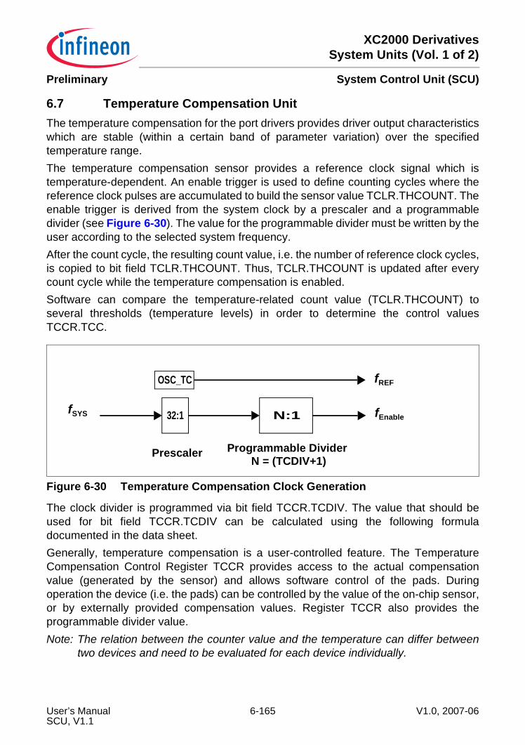
XC2000 DerivativesSystem Units (Vol. 1 of 2)
System Control Unit (SCU)Preliminary
6.7 Temperature Compensation Unit The temperature compensation for the port drivers provides driver output characteristicswhich are stable (within a certain band of parameter variation) over the specifiedtemperature range.The temperature compensation sensor provides a reference clock signal which istemperature-dependent. An enable trigger is used to define counting cycles where thereference clock pulses are accumulated to build the sensor value TCLR.THCOUNT. Theenable trigger is derived from the system clock by a prescaler and a programmabledivider (see Figure 6-30). The value for the programmable divider must be written by theuser according to the selected system frequency.After the count cycle, the resulting count value, i.e. the number of reference clock cycles,is copied to bit field TCLR.THCOUNT. Thus, TCLR.THCOUNT is updated after everycount cycle while the temperature compensation is enabled.Software can compare the temperature-related count value (TCLR.THCOUNT) toseveral thresholds (temperature levels) in order to determine the control valuesTCCR.TCC.
Figure 6-30 Temperature Compensation Clock Generation
The clock divider is programmed via bit field TCCR.TCDIV. The value that should beused for bit field TCCR.TCDIV can be calculated using the following formuladocumented in the data sheet.Generally, temperature compensation is a user-controlled feature. The TemperatureCompensation Control Register TCCR provides access to the actual compensationvalue (generated by the sensor) and allows software control of the pads. Duringoperation the device (i.e. the pads) can be controlled by the value of the on-chip sensor,or by externally provided compensation values. Register TCCR also provides theprogrammable divider value.Note: The relation between the counter value and the temperature can differ between
two devices and need to be evaluated for each device individually.
32:1 N:1
Prescaler Programmable Divider
fEnablefSYS
N = (TCDIV+1)
OSC_TC fREF
User’s Manual 6-165 V1.0, 2007-06SCU, V1.1
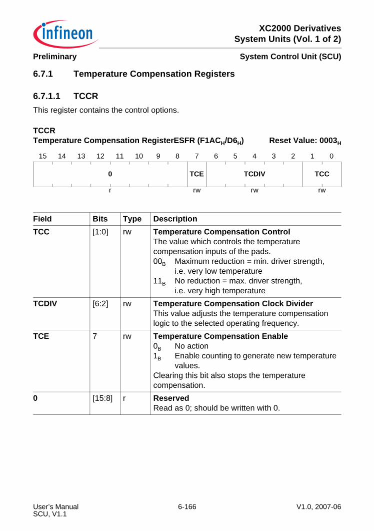
XC2000 DerivativesSystem Units (Vol. 1 of 2)
System Control Unit (SCU)Preliminary
6.7.1 Temperature Compensation Registers
6.7.1.1 TCCRThis register contains the control options.
TCCRTemperature Compensation RegisterESFR (F1ACH/D6H) Reset Value: 0003H
15 14 13 12 11 10 9 8 7 6 5 4 3 2 1 0
0 TCE TCDIV TCC
r rw rw rw
Field Bits Type DescriptionTCC [1:0] rw Temperature Compensation Control
The value which controls the temperature compensation inputs of the pads.00B Maximum reduction = min. driver strength,
i.e. very low temperature11B No reduction = max. driver strength,
i.e. very high temperatureTCDIV [6:2] rw Temperature Compensation Clock Divider
This value adjusts the temperature compensation logic to the selected operating frequency.
TCE 7 rw Temperature Compensation Enable0B No action1B Enable counting to generate new temperature
values.Clearing this bit also stops the temperature compensation.
0 [15:8] r ReservedRead as 0; should be written with 0.
User’s Manual 6-166 V1.0, 2007-06SCU, V1.1
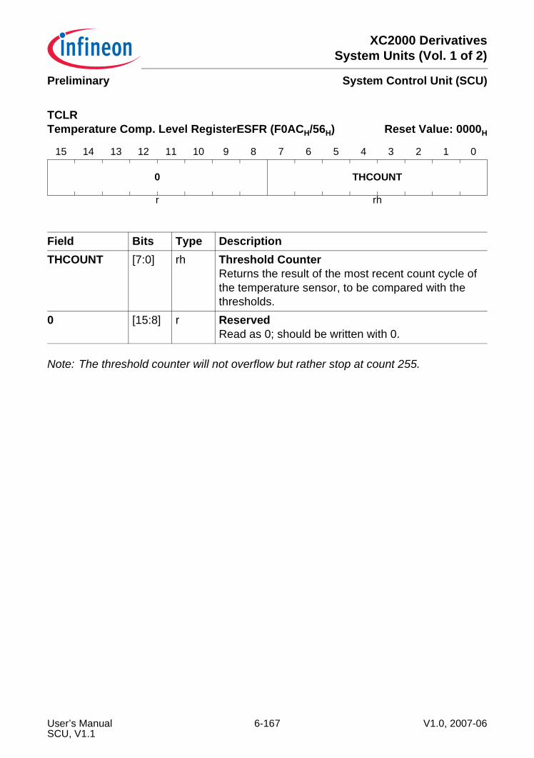
XC2000 DerivativesSystem Units (Vol. 1 of 2)
System Control Unit (SCU)Preliminary
Note: The threshold counter will not overflow but rather stop at count 255.
TCLRTemperature Comp. Level RegisterESFR (F0ACH/56H) Reset Value: 0000H
15 14 13 12 11 10 9 8 7 6 5 4 3 2 1 0
0 THCOUNT
r rh
Field Bits Type DescriptionTHCOUNT [7:0] rh Threshold Counter
Returns the result of the most recent count cycle of the temperature sensor, to be compared with the thresholds.
0 [15:8] r ReservedRead as 0; should be written with 0.
User’s Manual 6-167 V1.0, 2007-06SCU, V1.1

XC2000 DerivativesSystem Units (Vol. 1 of 2)
System Control Unit (SCU)Preliminary
6.8 Watchdog TimerThe following part describes the WDT and its functionality.
6.8.1 IntroductionThe Watchdog Timer (WDT) is a secure mechanism to overcome life- and dead-locks.An enabled WDT generates a reset for the system if not serviced in a configured timeframe.
FeaturesThe following list is a summary of the WDT functions:• 16-bit Watchdog Timer• Selectable operating frequency: fIN / 256 or fIN / 16384• Timer overflow error detection• Individual disable for timer functionality• Double Reset DetectionFigure 6-31 provides an overview on the registers of the Watchdog Timer.
Figure 6-31 Watchdog Timer Register Overview
6.8.2 OverviewThe Watchdog Timer (WDT) provides a highly reliable and secure way to detect andrecover from software or hardware failure. The WDT helps to abort an accidentalmalfunction of the XC2000 in a user-specified time period. When enabled, the WDT willcause the XC2000 system to be reset if the WDT is not serviced within a user-programmable time period. The CPU must service the WDT within this time interval toprevent the WDT from causing a WDT reset request trigger. Hence, regular service ofthe WDT confirms that the system is functioning properly.A further enhancement in the Watchdog Timer is its reset prewarning operation. Insteadof immediately resetting the device on the detection of an error, a prewarning output isgiven to the system via an interrupt request. This makes it possible to bring the systeminto a defined and predictable status, before the reset is finally issued.
WDT_Reg_Overview.vsd
WDTCS
W DT Control &Status Register
WDTCSWDTRELWDTTIM
WDT Control and Status RegisterWDT Reload RegisterWDT Timer Register
WDTTIM
W DT TimerRegister
WDTREL
W DT ReloadRegister
User’s Manual 6-168 V1.0, 2007-06SCU, V1.1
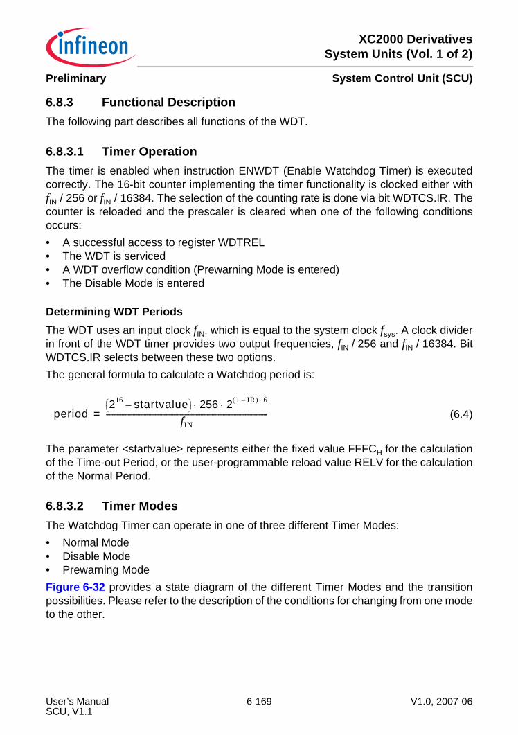
XC2000 DerivativesSystem Units (Vol. 1 of 2)
System Control Unit (SCU)Preliminary
6.8.3 Functional DescriptionThe following part describes all functions of the WDT.
6.8.3.1 Timer OperationThe timer is enabled when instruction ENWDT (Enable Watchdog Timer) is executedcorrectly. The 16-bit counter implementing the timer functionality is clocked either withfIN / 256 or fIN / 16384. The selection of the counting rate is done via bit WDTCS.IR. Thecounter is reloaded and the prescaler is cleared when one of the following conditionsoccurs:• A successful access to register WDTREL• The WDT is serviced• A WDT overflow condition (Prewarning Mode is entered)• The Disable Mode is entered
Determining WDT PeriodsThe WDT uses an input clock fIN, which is equal to the system clock fsys. A clock dividerin front of the WDT timer provides two output frequencies, fIN / 256 and fIN / 16384. BitWDTCS.IR selects between these two options.The general formula to calculate a Watchdog period is:
(6.4)
The parameter <startvalue> represents either the fixed value FFFCH for the calculationof the Time-out Period, or the user-programmable reload value RELV for the calculationof the Normal Period.
6.8.3.2 Timer ModesThe Watchdog Timer can operate in one of three different Timer Modes:• Normal Mode• Disable Mode• Prewarning ModeFigure 6-32 provides a state diagram of the different Timer Modes and the transitionpossibilities. Please refer to the description of the conditions for changing from one modeto the other.
period216 startvalue–⎝ ⎠
⎛ ⎞ 256 2 1 IR–( ) 6⋅⋅ ⋅
fIN-----------------------------------------------------------------------------------------------------------------------------------=
User’s Manual 6-169 V1.0, 2007-06SCU, V1.1
XC2000 DerivativesSystem Units (Vol. 1 of 2)
System Control Unit (SCU)Preliminary
Figure 6-32 State Diagram of the Timer Modes
Normal ModeThe Normal Mode is the default mode after an application reset. Normal Mode can beentered from Disable Mode only when instruction ENWDT is executed. The timer isloaded with RELV when the Normal Mode is entered, and it starts counting upwards.After reset, the timer is loaded with FFFCH, and it starts counting upwards. It has to beserviced before the counter overflows. Servicing is performed by the CPU viainstructions SRVWDT and/or ENWDT.If the WDT is not serviced before the timer overflows, a system malfunction is assumed,a WDT error is generated, and Prewarning Mode is entered. A reset of the XC2000 isimminent and can no longer be stopped.
Table 6-17 Timer Periods in Normal ModeIS Reload
ValueMin. / Max.
Period Example@ fIN= 40 MHz
0 0000H min. 65535 × 16384 / fIN = 1073725440 / fIN 26.8 smax. 65536 × 16384 / fIN = 1073741824 / fIN 26.8 s
FFFEH min. 1 × 16384 / fIN = 16384 / fIN 410 µsmax. 2 × 16384 / fIN = 32768 / fIN 819 µs
WDT Reset TriggerWDTCS.OE set
NormalMode
Pre-WarningMode
DisableMode
ENWDT
ApplicationReset
Timeroverflow
DISWDT
WDT_modes
User’s Manual 6-170 V1.0, 2007-06SCU, V1.1
XC2000 DerivativesSystem Units (Vol. 1 of 2)
System Control Unit (SCU)Preliminary
Disable ModeDisable Mode is provided for applications that do not require the Watchdog Timerfunction. Disable Mode is entered when instruction DISWDT is executed, either beforeEnd-of-Init, if CPUCON1.WDTCTL = 0, or at any time, if CPUCON1.WDTCTL = 1. Thetimer is cleared in this mode. A transition from Disable Mode to Normal Mode isperformed when instruction ENWDT is executed while CPUCON1.WDTCTL = 1 Thetimer is reloaded and the prescalers are cleared on this transition.
Prewarning ModePrewarning Mode is entered always when a Watchdog error is detected. This is anoverflow in Normal Mode. Instead of immediately requesting a reset of the device, theWDT enables the system to enter a secure state by issuing the prewarning output beforethe reset occurs. Receiving the prewarning, the CPU and the system are requested tofinish all pending transaction requests and to not generate new ones. The prewarning issignalled via an interrupt. The CPU can recognize the WDT prewarning interrupt viaregister INTSTAT. After finishing all pending transactions, the CPU should execute theIDLE instruction to stop all further processing before the coming reset.In Prewarning mode, the WDT starts counting from FFFFH upwards, and then requestsa WDT reset on the overflow. This reset request - and following reset generation - cannot be avoided in this mode; the WDT does not react anymore to accesses to itsregisters, nor will it change its state until it is reset.A feature of the WDT detects double errors and sets the whole system into a permanentWDT reset. This feature prevents the XC2000 from executing random wrong code forlonger than the Time-out Period, and prevents the XC2000 from being repeatedly resetby the WDT.Double WDT errors are detected with the aid of the error-indication flag WDTCS.OE.Servicing the WDT automatically clears this bit. However, this bit is not cleared when areset is caused by the WDT reset. Because the error bit is preserved across resetsrequested by the WDT, the WDT can examine if an overflow occurs again. If bitWDTCS.OE is still set when a new WDT overflow occurs, then there must have been apreceding WDT reset without a software service of the WDT in the meantime. Hence,
1 0000H min. 65535 × 256 / fIN = 16776960 / fIN 419 msmax. 65536 × 256 / fIN = 16777216 / fIN 419 ms
FFFEH min. 1 × 256 / fIN = 256 / fIN 6.4 µsmax. 2 × 256 / fIN = 512 / fIN 12.8 µs
Table 6-17 Timer Periods in Normal ModeIS Reload
ValueMin. / Max.
Period Example@ fIN= 40 MHz
User’s Manual 6-171 V1.0, 2007-06SCU, V1.1
XC2000 DerivativesSystem Units (Vol. 1 of 2)
System Control Unit (SCU)Preliminary
this is a double WDT error condition. In this case, the WDT will generate another resetafter the termination of the Prewarning Mode, but this time, the XC2000 will be held inthe reset state until a power-up reset is generated by external hardware.Note: Double WDT errors can only occur if the WDT reset is not configured to generate
a system reset.
6.8.3.3 WDT during Power-Saving ModesDuring Offline Mode, the WDT cannot be serviced. Excluding the case where the systemis running normally, a strategy for managing the WDT is needed for the Offline Mode.There are two ways to handle the WDT in this case. First, the WDT can be disabled before going into Offline Mode. This has thedisadvantage that the system will no longer be monitored during the Offline period.Second, the time the system stays in the Offline Mode can be configured with the wake-up timer in a way that the system is switched back to Active Mode before the WDT needsto be serviced. Then the CPU can service the WDT again and return to the Offline Mode.Note: Before switching into a non-running power-management mode, software should
perform a Watchdog service sequence. The Watchdog reload value RELV inregister WDTREL should be programmed such that the wake-up occurs after aperiod which best meets application requirements.
6.8.3.4 Suspend Mode SupportIn an enabled and active debug session, the Watchdog functionality can lead tounintended resets. Therefore, to avoid these resets, the OCDS can control whether theWDT is enabled or disabled (default after reset). This is done via bit CBS_IOSR.DB.
Table 6-18 OCDS Behavior of WDTWDTCS.DS CBS_DBGSR.DBGEN CBS_IOSR.DB WDT Action1 X X Stopped0 0 X Running0 1 0 Stopped0 1 1 Running
User’s Manual 6-172 V1.0, 2007-06SCU, V1.1
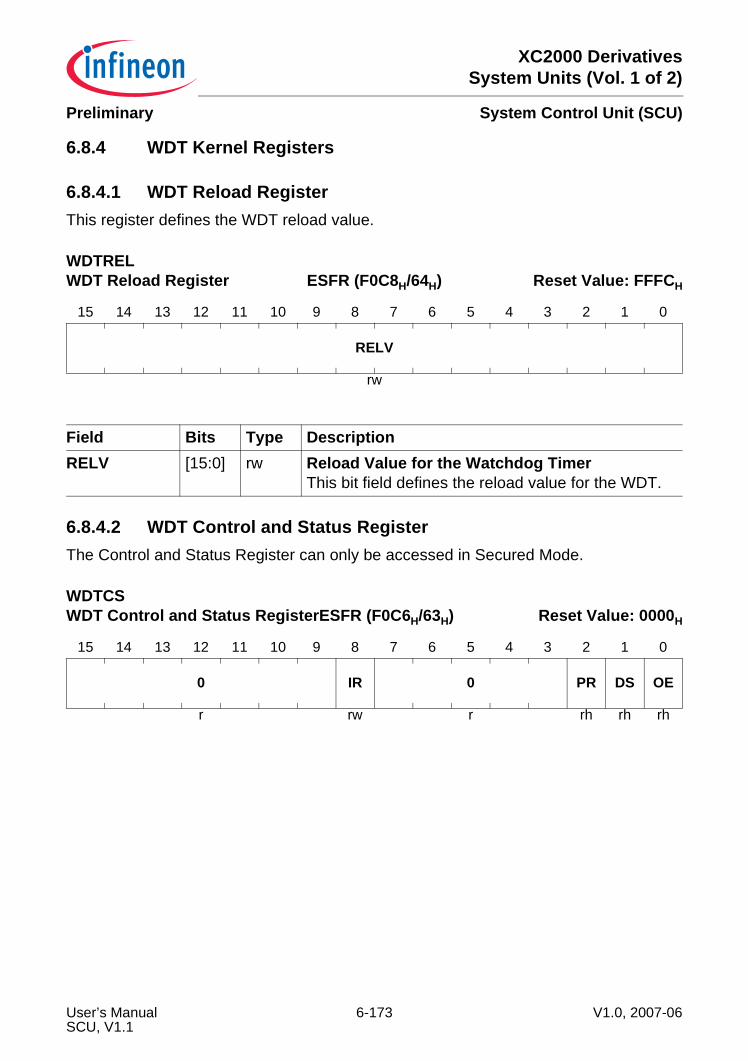
XC2000 DerivativesSystem Units (Vol. 1 of 2)
System Control Unit (SCU)Preliminary
6.8.4 WDT Kernel Registers
6.8.4.1 WDT Reload RegisterThis register defines the WDT reload value.
6.8.4.2 WDT Control and Status RegisterThe Control and Status Register can only be accessed in Secured Mode.
WDTRELWDT Reload Register ESFR (F0C8H/64H) Reset Value: FFFCH
15 14 13 12 11 10 9 8 7 6 5 4 3 2 1 0
RELV
rw
Field Bits Type DescriptionRELV [15:0] rw Reload Value for the Watchdog Timer
This bit field defines the reload value for the WDT.
WDTCSWDT Control and Status RegisterESFR (F0C6H/63H) Reset Value: 0000H
15 14 13 12 11 10 9 8 7 6 5 4 3 2 1 0
0 IR 0 PR DS OE
r rw r rh rh rh
User’s Manual 6-173 V1.0, 2007-06SCU, V1.1
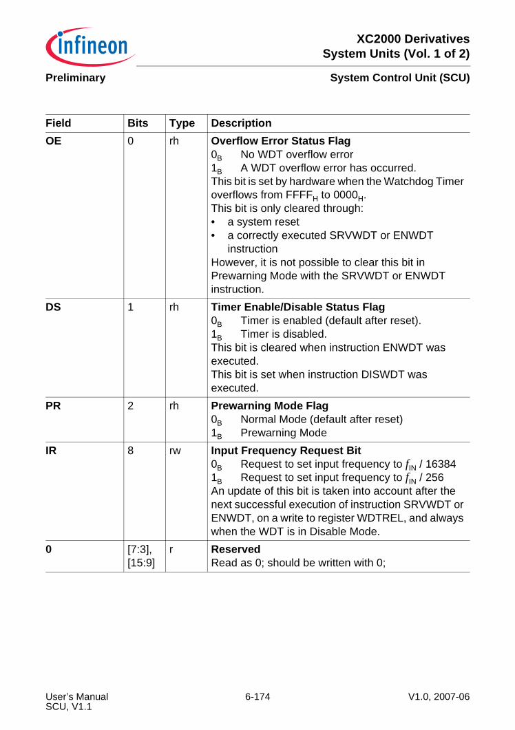
XC2000 DerivativesSystem Units (Vol. 1 of 2)
System Control Unit (SCU)Preliminary
Field Bits Type DescriptionOE 0 rh Overflow Error Status Flag
0B No WDT overflow error1B A WDT overflow error has occurred.This bit is set by hardware when the Watchdog Timer overflows from FFFFH to 0000H. This bit is only cleared through:• a system reset• a correctly executed SRVWDT or ENWDT
instructionHowever, it is not possible to clear this bit in Prewarning Mode with the SRVWDT or ENWDT instruction.
DS 1 rh Timer Enable/Disable Status Flag0B Timer is enabled (default after reset).1B Timer is disabled.This bit is cleared when instruction ENWDT was executed.This bit is set when instruction DISWDT was executed.
PR 2 rh Prewarning Mode Flag0B Normal Mode (default after reset)1B Prewarning Mode
IR 8 rw Input Frequency Request Bit0B Request to set input frequency to fIN / 163841B Request to set input frequency to fIN / 256An update of this bit is taken into account after the next successful execution of instruction SRVWDT or ENWDT, on a write to register WDTREL, and always when the WDT is in Disable Mode.
0 [7:3],[15:9]
r ReservedRead as 0; should be written with 0;
User’s Manual 6-174 V1.0, 2007-06SCU, V1.1
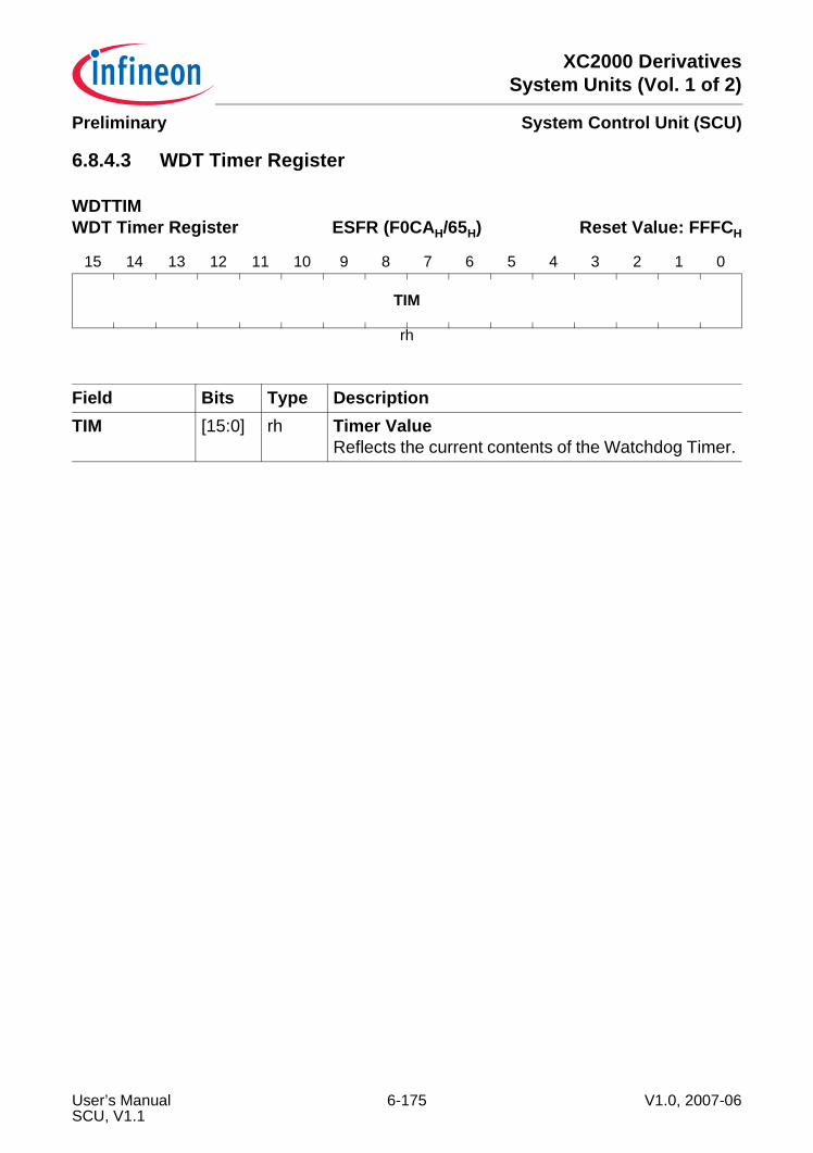
XC2000 DerivativesSystem Units (Vol. 1 of 2)
System Control Unit (SCU)Preliminary
6.8.4.3 WDT Timer Register
WDTTIMWDT Timer Register ESFR (F0CAH/65H) Reset Value: FFFCH
15 14 13 12 11 10 9 8 7 6 5 4 3 2 1 0
TIM
rh
Field Bits Type DescriptionTIM [15:0] rh Timer Value
Reflects the current contents of the Watchdog Timer.
User’s Manual 6-175 V1.0, 2007-06SCU, V1.1
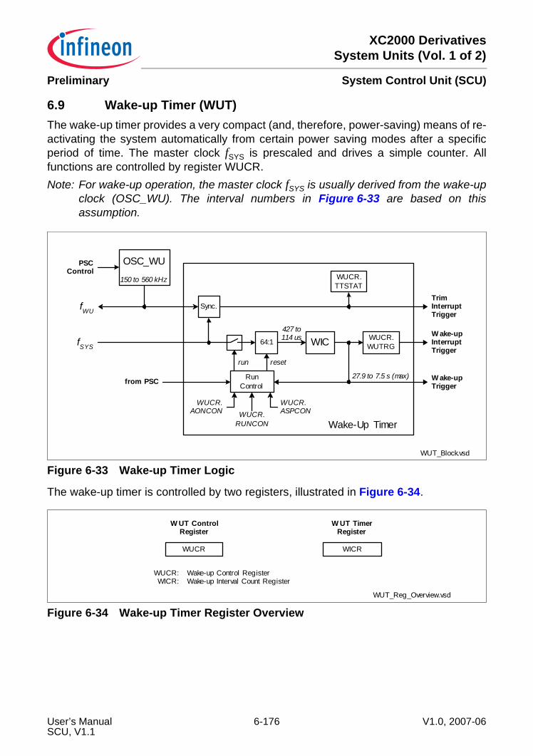
XC2000 DerivativesSystem Units (Vol. 1 of 2)
System Control Unit (SCU)Preliminary
6.9 Wake-up Timer (WUT)The wake-up timer provides a very compact (and, therefore, power-saving) means of re-activating the system automatically from certain power saving modes after a specificperiod of time. The master clock fSYS is prescaled and drives a simple counter. Allfunctions are controlled by register WUCR.Note: For wake-up operation, the master clock fSYS is usually derived from the wake-up
clock (OSC_WU). The interval numbers in Figure 6-33 are based on thisassumption.
Figure 6-33 Wake-up Timer Logic
The wake-up timer is controlled by two registers, illustrated in Figure 6-34.
Figure 6-34 Wake-up Timer Register Overview
WUT_Block.vsd
OSC_WU
27.9 to 7.5 s (max)
Sync.
fSYS64:1 WIC WUCR.
WUTRG
427 to114 us
TrimInterruptTrigger
W ake-upTrigger
W ake-upInterruptTrigger
fWU
RunControl
reset
WUCR.AONCON
WUCR.ASPCON
WUCR.TTSTAT
150 to 560 kHz
Wake-Up Timer
from PSC
WUCR.RUNCON
run
PSCControl
WUT_Reg_Overview.vsd
WUCR
W UT ControlRegister
WUCR:WICR:
Wake-up Control RegisterWake-up Interval Count Register
WICR
W UT TimerRegister
User’s Manual 6-176 V1.0, 2007-06SCU, V1.1
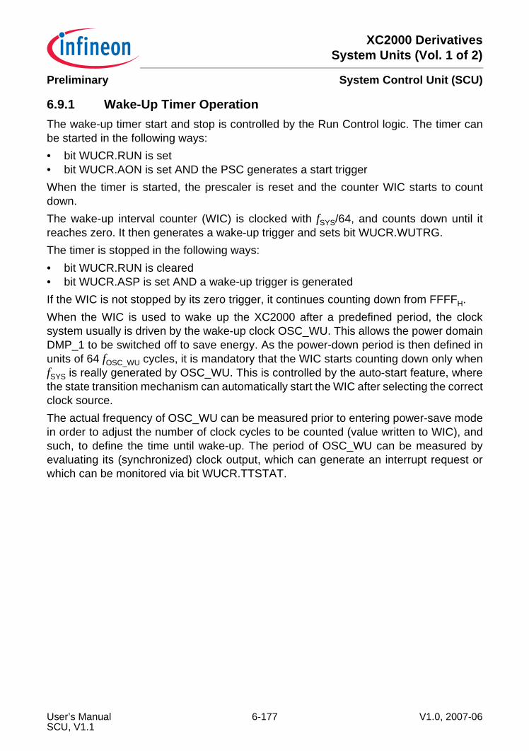
XC2000 DerivativesSystem Units (Vol. 1 of 2)
System Control Unit (SCU)Preliminary
6.9.1 Wake-Up Timer OperationThe wake-up timer start and stop is controlled by the Run Control logic. The timer canbe started in the following ways:• bit WUCR.RUN is set• bit WUCR.AON is set AND the PSC generates a start triggerWhen the timer is started, the prescaler is reset and the counter WIC starts to countdown.The wake-up interval counter (WIC) is clocked with fSYS/64, and counts down until itreaches zero. It then generates a wake-up trigger and sets bit WUCR.WUTRG.The timer is stopped in the following ways:• bit WUCR.RUN is cleared• bit WUCR.ASP is set AND a wake-up trigger is generatedIf the WIC is not stopped by its zero trigger, it continues counting down from FFFFH.When the WIC is used to wake up the XC2000 after a predefined period, the clocksystem usually is driven by the wake-up clock OSC_WU. This allows the power domainDMP_1 to be switched off to save energy. As the power-down period is then defined inunits of 64 fOSC_WU cycles, it is mandatory that the WIC starts counting down only whenfSYS is really generated by OSC_WU. This is controlled by the auto-start feature, wherethe state transition mechanism can automatically start the WIC after selecting the correctclock source.The actual frequency of OSC_WU can be measured prior to entering power-save modein order to adjust the number of clock cycles to be counted (value written to WIC), andsuch, to define the time until wake-up. The period of OSC_WU can be measured byevaluating its (synchronized) clock output, which can generate an interrupt request orwhich can be monitored via bit WUCR.TTSTAT.
User’s Manual 6-177 V1.0, 2007-06SCU, V1.1
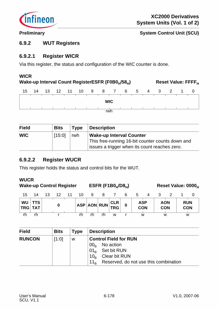
XC2000 DerivativesSystem Units (Vol. 1 of 2)
System Control Unit (SCU)Preliminary
6.9.2 WUT Registers
6.9.2.1 Register WICRVia this register, the status and configuration of the WIC counter is done.
6.9.2.2 Register WUCRThis register holds the status and control bits for the WUT.
WICRWake-up Interval Count RegisterESFR (F0B0H/58H) Reset Value: FFFFH
15 14 13 12 11 10 9 8 7 6 5 4 3 2 1 0
WIC
rwh
Field Bits Type DescriptionWIC [15:0] rwh Wake-up Interval Counter
This free-running 16-bit counter counts down and issues a trigger when its count reaches zero.
WUCRWake-up Control Register ESFR (F1B0H/D8H) Reset Value: 0000H
15 14 13 12 11 10 9 8 7 6 5 4 3 2 1 0
WUTRG
TTSTAT 0 ASP AON RUN CLR
TRG 0 ASPCON
AONCON
RUNCON
rh rh r rh rh rh w r w w w
Field Bits Type DescriptionRUNCON [1:0] w Control Field for RUN
00B No action01B Set bit RUN10B Clear bit RUN11B Reserved, do not use this combination
User’s Manual 6-178 V1.0, 2007-06SCU, V1.1
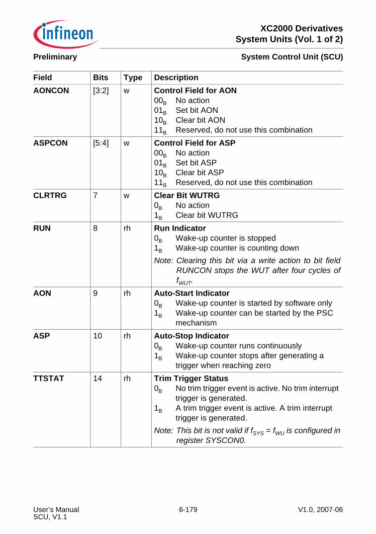
XC2000 DerivativesSystem Units (Vol. 1 of 2)
System Control Unit (SCU)Preliminary
AONCON [3:2] w Control Field for AON00B No action01B Set bit AON10B Clear bit AON11B Reserved, do not use this combination
ASPCON [5:4] w Control Field for ASP00B No action01B Set bit ASP10B Clear bit ASP11B Reserved, do not use this combination
CLRTRG 7 w Clear Bit WUTRG0B No action1B Clear bit WUTRG
RUN 8 rh Run Indicator0B Wake-up counter is stopped1B Wake-up counter is counting downNote: Clearing this bit via a write action to bit field
RUNCON stops the WUT after four cycles offWUT.
AON 9 rh Auto-Start Indicator0B Wake-up counter is started by software only1B Wake-up counter can be started by the PSC
mechanismASP 10 rh Auto-Stop Indicator
0B Wake-up counter runs continuously1B Wake-up counter stops after generating a
trigger when reaching zeroTTSTAT 14 rh Trim Trigger Status
0B No trim trigger event is active. No trim interrupt trigger is generated.
1B A trim trigger event is active. A trim interrupt trigger is generated.
Note: This bit is not valid if fSYS = fWU is configured inregister SYSCON0.
Field Bits Type Description
User’s Manual 6-179 V1.0, 2007-06SCU, V1.1
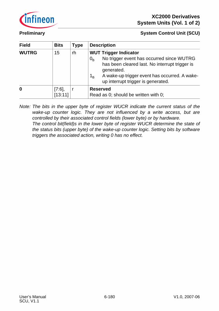
XC2000 DerivativesSystem Units (Vol. 1 of 2)
System Control Unit (SCU)Preliminary
Note: The bits in the upper byte of register WUCR indicate the current status of thewake-up counter logic. They are not influenced by a write access, but arecontrolled by their associated control fields (lower byte) or by hardware.The control bit(field)s in the lower byte of register WUCR determine the state ofthe status bits (upper byte) of the wake-up counter logic. Setting bits by softwaretriggers the associated action, writing 0 has no effect.
WUTRG 15 rh WUT Trigger Indicator0B No trigger event has occurred since WUTRG
has been cleared last. No interrupt trigger is generated.
1B A wake-up trigger event has occurred. A wake-up interrupt trigger is generated.
0 [7:6],[13:11]
r ReservedRead as 0; should be written with 0;
Field Bits Type Description
User’s Manual 6-180 V1.0, 2007-06SCU, V1.1
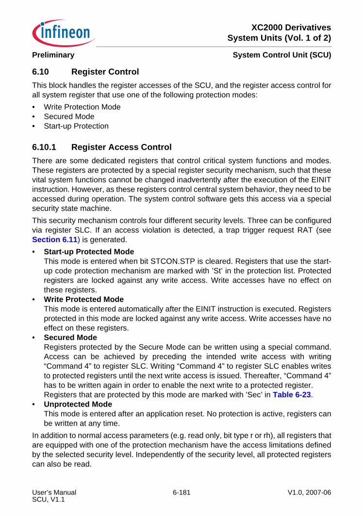
XC2000 DerivativesSystem Units (Vol. 1 of 2)
System Control Unit (SCU)Preliminary
6.10 Register ControlThis block handles the register accesses of the SCU, and the register access control forall system register that use one of the following protection modes:• Write Protection Mode• Secured Mode• Start-up Protection
6.10.1 Register Access ControlThere are some dedicated registers that control critical system functions and modes.These registers are protected by a special register security mechanism, such that thesevital system functions cannot be changed inadvertently after the execution of the EINITinstruction. However, as these registers control central system behavior, they need to beaccessed during operation. The system control software gets this access via a specialsecurity state machine.This security mechanism controls four different security levels. Three can be configuredvia register SLC. If an access violation is detected, a trap trigger request RAT (seeSection 6.11) is generated.• Start-up Protected Mode
This mode is entered when bit STCON.STP is cleared. Registers that use the start-up code protection mechanism are marked with ’St’ in the protection list. Protectedregisters are locked against any write access. Write accesses have no effect onthese registers.
• Write Protected ModeThis mode is entered automatically after the EINIT instruction is executed. Registersprotected in this mode are locked against any write access. Write accesses have noeffect on these registers.
• Secured ModeRegisters protected by the Secure Mode can be written using a special command.Access can be achieved by preceding the intended write access with writing“Command 4” to register SLC. Writing “Command 4” to register SLC enables writesto protected registers until the next write access is issued. Thereafter, “Command 4”has to be written again in order to enable the next write to a protected register.Registers that are protected by this mode are marked with ’Sec’ in Table 6-23.
• Unprotected Mode This mode is entered after an application reset. No protection is active, registers canbe written at any time.
In addition to normal access parameters (e.g. read only, bit type r or rh), all registers thatare equipped with one of the protection mechanism have the access limitations definedby the selected security level. Independently of the security level, all protected registerscan also be read.
User’s Manual 6-181 V1.0, 2007-06SCU, V1.1
XC2000 DerivativesSystem Units (Vol. 1 of 2)
System Control Unit (SCU)Preliminary
6.10.1.1 Controlling the Security LevelTwo registers, the Security Level Command register (SLC) and the Security Level Statusregister (SLS), control the security level. The SLC register accepts the commands tocontrol the state machine modifying the security level, while the SLS register shows theactual password, the actual security level, and the state of the state machine.
Figure 6-35 State Machine for Security Level Controlling
The following mechanism is used to control the actual security level:• Changing the security level
can be done by executing the following command sequence:“Command 0 - Command 1 - Command 2 - Command 3”.This sequence establishes a new security level and/or a new password.
Note: It is recommended to lock all command sequences with an atomic sequence.
Table 6-19 Commands for Security Level ControlCommand Definition NoteCommand 0 AAAAH
Command 1 5554H
Command 2 96H || <inverse password>Command 3 000B || <new level> || 000B || <new password>Command 4 8EH || <inverse password> Secured Mode only
Sta te 0
Sta te 1
Command 3 or any write access
Com
man
d 0
Command 1or any write access
Command 1State 4
Class 3 Reset
Command 4
Any write access
Sta te 3
Sta te 2
Command 2or any write access
Com
man
d 2
MCA05336
User’s Manual 6-182 V1.0, 2007-06SCU, V1.1
XC2000 DerivativesSystem Units (Vol. 1 of 2)
System Control Unit (SCU)Preliminary
6.10.2 Register Protection Registers
6.10.2.1 Register SLCThis register is the interface for the protection commands.
SLCSecurity Level Command RegisterESFR (F0C0H/60H) Reset Value: 0000H
15 14 13 12 11 10 9 8 7 6 5 4 3 2 1 0
COMMAND
rw
Field Bits Type DescriptionCOMMAND [15:0] rw Security Level Control Command
The commands to control the security level must be written to this register (see Table 6-19)
User’s Manual 6-183 V1.0, 2007-06SCU, V1.1
XC2000 DerivativesSystem Units (Vol. 1 of 2)
System Control Unit (SCU)Preliminary
6.10.2.2 Register SLSThis register reflects the status of the register protection.
SLSSecurity Level Status Register ESFR (F0C2H/61H) Reset Value: 0000H
15 14 13 12 11 10 9 8 7 6 5 4 3 2 1 0
STATE SL 0 PASSWORD
rh rh r rh
Field Bits Type DescriptionPASSWORD [7:0] rh Current Security Control Password
Default after reset = 00H
SL [12:11] rh Security Level 1)
00B Unprotected Mode (default)01B Secured Mode10B Reserved, do not use this combination11B Write Protected Mode
1) While the security level is “unprotected” after reset, it changes to “write protected” after the execution ofinstruction EINIT.
STATE [15:13] rh Current State of Switching State Machine000B Awaiting command 0 or command 4 (default)001B Awaiting command 1010B Awaiting command 2011B Awaiting new security level and password100B Next access granted in Secured Mode101B Reserved, do not use this combination11XB Reserved, do not use this combination
0 [10:8] r ReservedRead as 0; should be written with 0;
User’s Manual 6-184 V1.0, 2007-06SCU, V1.1

XC2000 DerivativesSystem Units (Vol. 1 of 2)
System Control Unit (SCU)Preliminary
6.10.3 Miscellaneous System Control Registers
6.10.3.1 System Control RegistersThe following register serves for various system tasks.
SYSCON1System Control 1 Register SFR (FF4CH/A6H) Reset Value: 0003H
15 14 13 12 11 10 9 8 7 6 5 4 3 2 1 0
0 GLCCST
OCDSEN 0
r rw rw rw
Field Bits Type DescriptionOCDSEN 2 rw OCDS/Cerberus Enable
0B OCDS and Cerberus are still in reset state1B ODCS and Cerberus are operable
GLCCST 3 rw Global CAPCOM StartBit GLCCST starts all CAPCOM units synchronously, if enabled. 0B CAPCOM timer start is controlled locally in
each unit1B All CAPCOM timers are started synchronouslyGLCCST is automatically cleared in the clock cycle after it was set.
0 [1:0] rw ReservedShould be written with 0.
0 [15:4] r ReservedRead as 0; should be written with 0.
User’s Manual 6-185 V1.0, 2007-06SCU, V1.1

XC2000 DerivativesSystem Units (Vol. 1 of 2)
System Control Unit (SCU)Preliminary
6.11 SCU Interrupt and Trap HandlingThe SCU handles a number of interrupts and traps. It contains appropriate logic andregisters to enable/disable the request sources, to hold the request flags, to set or clearthe flags, and to distribute the requests to a given interrupt or trap node.The interrupt structure is detailed in Section 6.11.1, while the trap structure is explainedin Section 6.11.3.In order to not loose interrupts or traps during a power-save mode, a number of interruptand trap requests are fed through a sticky flag register in the DMP_M domain, beforebeing connected to the SCU interrupt or trap handling structure. In this way, theoccurrence of an event is registered even when the DMP_1 domain is powered down.Details about this structure can be found in Section 6.11.5.An additional part of the SCU structure facilitates the mapping of the interrupt requestsources in the system to the sixteen interrupt nodes CC2_CCxIC. These interrupt nodesare shared between the CC2 and other interrupt sources. Details can be found inSection 6.11.7.Figure 6-36 provides an overview on the SCU interrupt and trap handling, whileFigure 6-37 shows the registers involved.
Figure 6-36 SCU Interrupt and Trap OverviewSCU_Trap_Int_Overview.vsd
SCU InterruptStructure
TrapEvents
InterruptEvents
Int. & TrapTrigger Reg.
DMPMIT
SCU TrapStructure
DMP_MDomain
1
9
4
4 Trap StatusRegister
TRAPSTAT
Interrupt StatusRegisterINTSTAT
9
4
16
10
Alternate InterruptAssignment Register
ISSR
16to 16 ITC NodesCC2_CC16IC..CC2_CC31IC
CC2InterruptSources
USIC & ERUInterruptSources
9
4
disable
disable
request
request
SCU_IRQ0
SCU_IRQ1
to ITC Node 6C H
to ITC Node 6BH
to TFR.ACER
to TFR.SR1
to TFR.SR0
SCU_TRQ0
SCU_TRQ1
SCU_TRQ2
DMP_1Domain
requ
est
requ
est
requ
est
requ
est
User’s Manual 6-186 V1.0, 2007-06SCU, V1.1
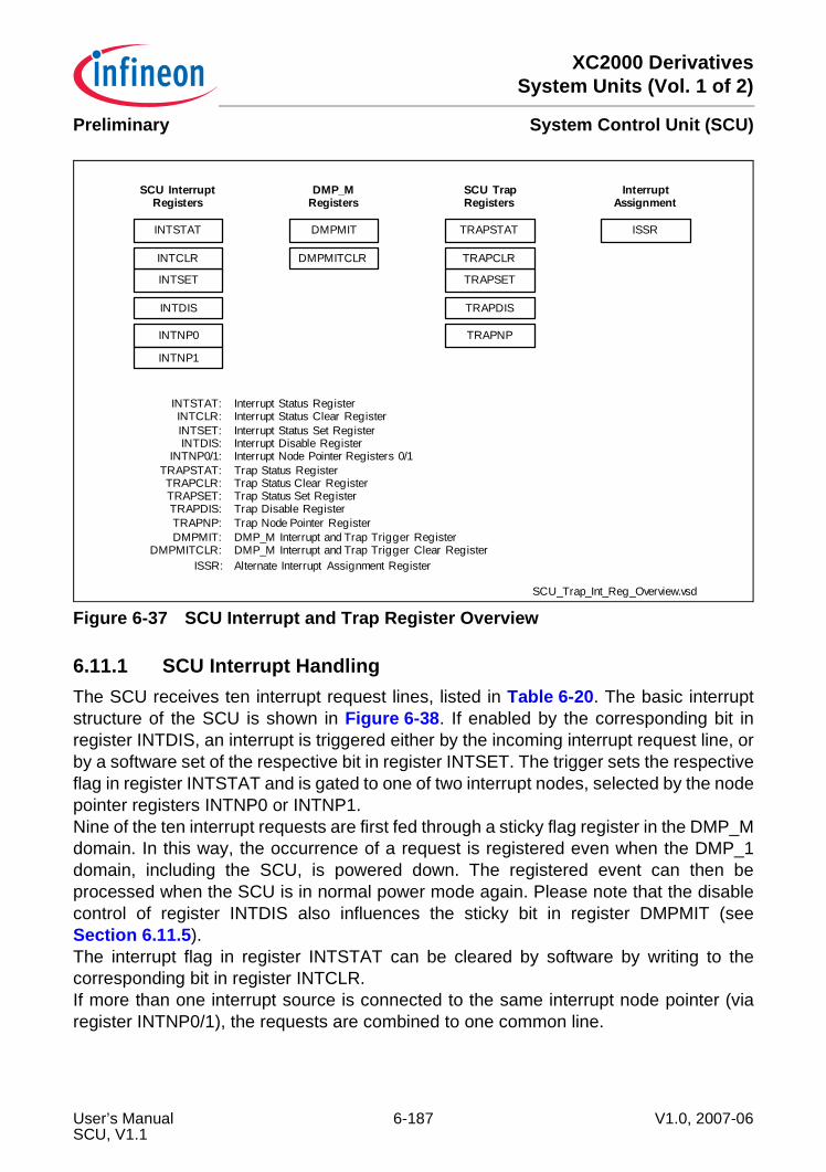
XC2000 DerivativesSystem Units (Vol. 1 of 2)
System Control Unit (SCU)Preliminary
Figure 6-37 SCU Interrupt and Trap Register Overview
6.11.1 SCU Interrupt HandlingThe SCU receives ten interrupt request lines, listed in Table 6-20. The basic interruptstructure of the SCU is shown in Figure 6-38. If enabled by the corresponding bit inregister INTDIS, an interrupt is triggered either by the incoming interrupt request line, orby a software set of the respective bit in register INTSET. The trigger sets the respectiveflag in register INTSTAT and is gated to one of two interrupt nodes, selected by the nodepointer registers INTNP0 or INTNP1.Nine of the ten interrupt requests are first fed through a sticky flag register in the DMP_Mdomain. In this way, the occurrence of a request is registered even when the DMP_1domain, including the SCU, is powered down. The registered event can then beprocessed when the SCU is in normal power mode again. Please note that the disablecontrol of register INTDIS also influences the sticky bit in register DMPMIT (seeSection 6.11.5).The interrupt flag in register INTSTAT can be cleared by software by writing to thecorresponding bit in register INTCLR.If more than one interrupt source is connected to the same interrupt node pointer (viaregister INTNP0/1), the requests are combined to one common line.
SCU_Trap_Int_Reg_Overview.vsd
SCU TrapRegisters
INTSTAT
INTSET
INTCLR
INTDIS
INTNP0
INTNP1
TRAPSTAT
TRAPSET
TRAPCLR
TRAPDIS
TRAPNP
DMPMIT
DMPMITCLR
SCU InterruptRegisters
DMP_MRegisters
INTSTAT:INTCLR:INTSET:INTDIS:
INTNP0/1:
Interrupt Status RegisterInterrupt Status Clear RegisterInterrupt Status Set RegisterInterrupt Disable RegisterInterrupt Node Pointer Registers 0/1
TRAPSTAT:TRAPCLR:TRAPSET:TRAPDIS:TRAPNP:
Trap Status RegisterTrap Status Clear RegisterTrap Status Set RegisterTrap Disable RegisterTrap Node Pointer Register
DMPMIT:DMPMITCLR:
DMP_M Interrupt and Trap Trigger RegisterDMP_M Interrupt and Trap Trigger Clear Register
ISSR
InterruptAssignment
ISSR: Alternate Interrupt Assignment Register
User’s Manual 6-187 V1.0, 2007-06SCU, V1.1
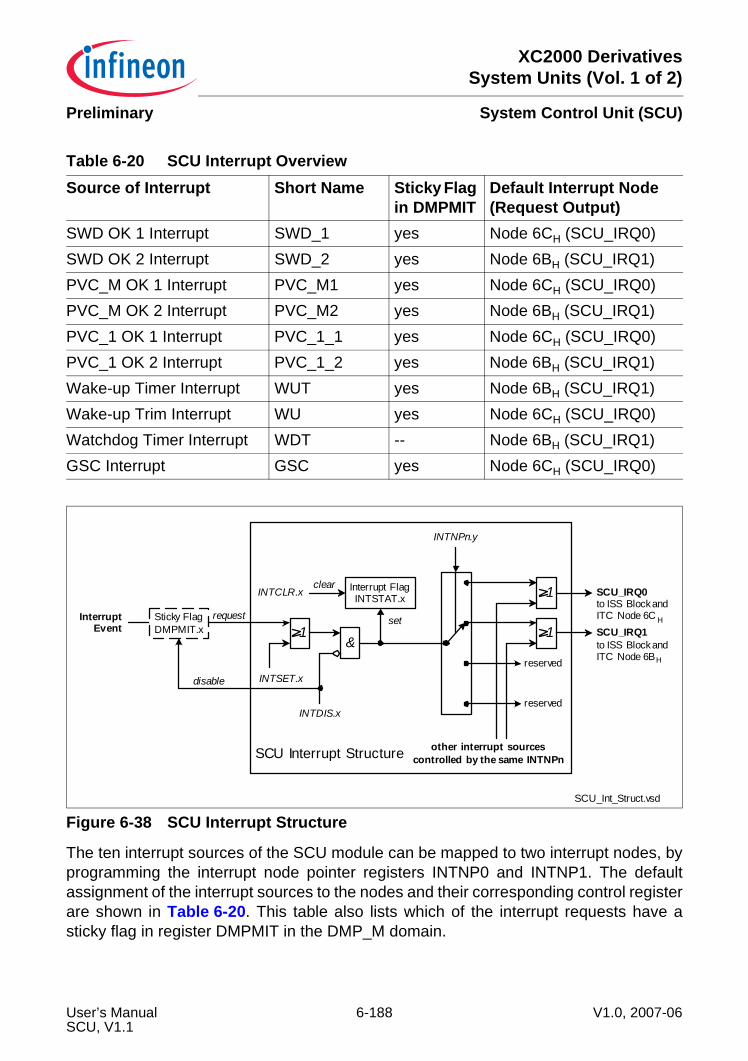
XC2000 DerivativesSystem Units (Vol. 1 of 2)
System Control Unit (SCU)Preliminary
Figure 6-38 SCU Interrupt Structure
The ten interrupt sources of the SCU module can be mapped to two interrupt nodes, byprogramming the interrupt node pointer registers INTNP0 and INTNP1. The defaultassignment of the interrupt sources to the nodes and their corresponding control registerare shown in Table 6-20. This table also lists which of the interrupt requests have asticky flag in register DMPMIT in the DMP_M domain.
Table 6-20 SCU Interrupt OverviewSource of Interrupt Short Name Sticky Flag
in DMPMITDefault Interrupt Node (Request Output)
SWD OK 1 Interrupt SWD_1 yes Node 6CH (SCU_IRQ0)SWD OK 2 Interrupt SWD_2 yes Node 6BH (SCU_IRQ1)PVC_M OK 1 Interrupt PVC_M1 yes Node 6CH (SCU_IRQ0)PVC_M OK 2 Interrupt PVC_M2 yes Node 6BH (SCU_IRQ1)PVC_1 OK 1 Interrupt PVC_1_1 yes Node 6CH (SCU_IRQ0)PVC_1 OK 2 Interrupt PVC_1_2 yes Node 6BH (SCU_IRQ1)Wake-up Timer Interrupt WUT yes Node 6BH (SCU_IRQ1)Wake-up Trim Interrupt WU yes Node 6CH (SCU_IRQ0)Watchdog Timer Interrupt WDT -- Node 6BH (SCU_IRQ1)GSC Interrupt GSC yes Node 6CH (SCU_IRQ0)
SCU_Int_Struct.vsd
INTSET.x
SCU Interrupt Structure
clear
other interrupt sourcescontrolled by the same INTNPn
&
1
1 1
Interrupt FlagINTSTAT.x
INTDIS.x
INTCLR.x
set
SCU_IRQ0
InterruptEvent
INTNPn.y
reserved
reserved
Sticky FlagDMPMIT.x SCU_IRQ1
to ISS Block andITC Node 6C H
to ISS Block andITC Node 6BH
disable
request
User’s Manual 6-188 V1.0, 2007-06SCU, V1.1
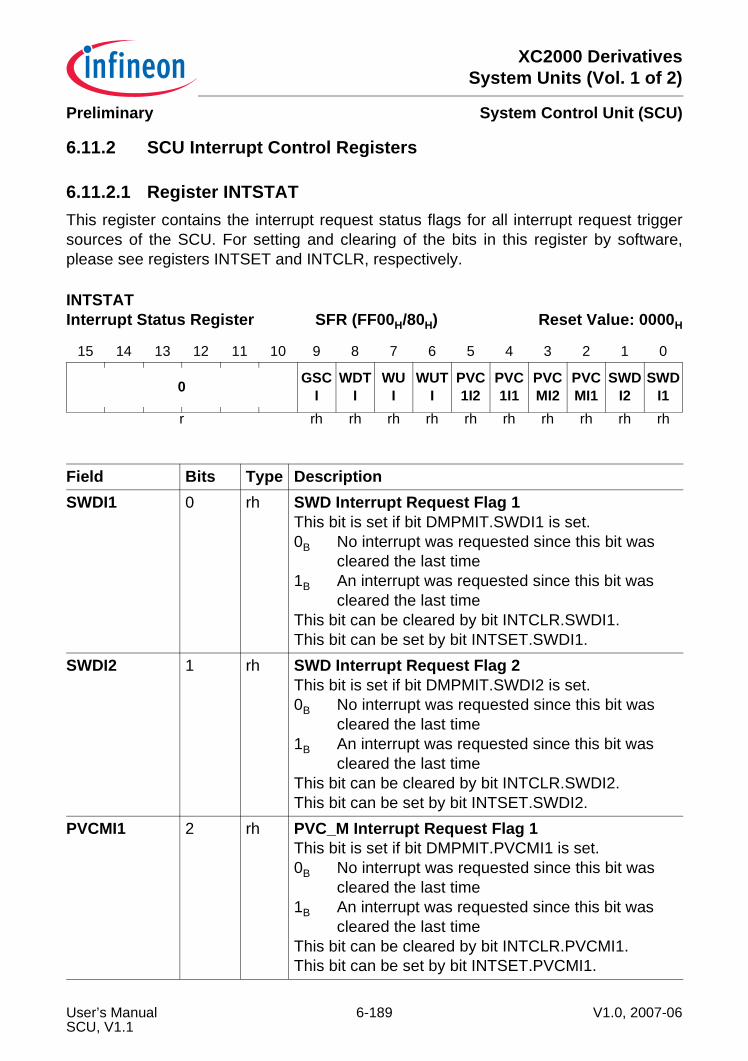
XC2000 DerivativesSystem Units (Vol. 1 of 2)
System Control Unit (SCU)Preliminary
6.11.2 SCU Interrupt Control Registers
6.11.2.1 Register INTSTATThis register contains the interrupt request status flags for all interrupt request triggersources of the SCU. For setting and clearing of the bits in this register by software,please see registers INTSET and INTCLR, respectively.
INTSTATInterrupt Status Register SFR (FF00H/80H) Reset Value: 0000H
15 14 13 12 11 10 9 8 7 6 5 4 3 2 1 0
0 GSCI
WDTI
WUI
WUTI
PVC1I2
PVC1I1
PVCMI2
PVCMI1
SWDI2
SWDI1
r rh rh rh rh rh rh rh rh rh rh
Field Bits Type DescriptionSWDI1 0 rh SWD Interrupt Request Flag 1
This bit is set if bit DMPMIT.SWDI1 is set.0B No interrupt was requested since this bit was
cleared the last time1B An interrupt was requested since this bit was
cleared the last timeThis bit can be cleared by bit INTCLR.SWDI1.This bit can be set by bit INTSET.SWDI1.
SWDI2 1 rh SWD Interrupt Request Flag 2This bit is set if bit DMPMIT.SWDI2 is set.0B No interrupt was requested since this bit was
cleared the last time1B An interrupt was requested since this bit was
cleared the last timeThis bit can be cleared by bit INTCLR.SWDI2.This bit can be set by bit INTSET.SWDI2.
PVCMI1 2 rh PVC_M Interrupt Request Flag 1This bit is set if bit DMPMIT.PVCMI1 is set.0B No interrupt was requested since this bit was
cleared the last time1B An interrupt was requested since this bit was
cleared the last timeThis bit can be cleared by bit INTCLR.PVCMI1.This bit can be set by bit INTSET.PVCMI1.
User’s Manual 6-189 V1.0, 2007-06SCU, V1.1
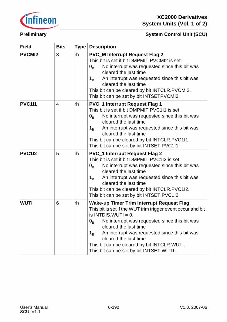
XC2000 DerivativesSystem Units (Vol. 1 of 2)
System Control Unit (SCU)Preliminary
PVCMI2 3 rh PVC_M Interrupt Request Flag 2This bit is set if bit DMPMIT.PVCMI2 is set.0B No interrupt was requested since this bit was
cleared the last time1B An interrupt was requested since this bit was
cleared the last timeThis bit can be cleared by bit INTCLR.PVCMI2.This bit can be set by bit INTSETPVCMI2.
PVC1I1 4 rh PVC_1 Interrupt Request Flag 1This bit is set if bit DMPMIT.PVC1I1 is set.0B No interrupt was requested since this bit was
cleared the last time1B An interrupt was requested since this bit was
cleared the last timeThis bit can be cleared by bit INTCLR.PVC1I1.This bit can be set by bit INTSET.PVC1I1.
PVC1I2 5 rh PVC_1 Interrupt Request Flag 2This bit is set if bit DMPMIT.PVC1I2 is set.0B No interrupt was requested since this bit was
cleared the last time1B An interrupt was requested since this bit was
cleared the last timeThis bit can be cleared by bit INTCLR.PVC1I2.This bit can be set by bit INTSET.PVC1I2.
WUTI 6 rh Wake-up Timer Trim Interrupt Request FlagThis bit is set if the WUT trim trigger event occur and bit is INTDIS.WUTI = 0.0B No interrupt was requested since this bit was
cleared the last time1B An interrupt was requested since this bit was
cleared the last timeThis bit can be cleared by bit INTCLR.WUTI.This bit can be set by bit INTSET.WUTI.
Field Bits Type Description
User’s Manual 6-190 V1.0, 2007-06SCU, V1.1

XC2000 DerivativesSystem Units (Vol. 1 of 2)
System Control Unit (SCU)Preliminary
WUI 7 rh Wake-up Timer Interrupt Request FlagThis bit is set if the WU trigger event occur and bit is INTDIS.WUI = 0.0B No interrupt was requested since this bit was
cleared the last time1B An interrupt was requested since this bit was
cleared the last timeThis bit can be cleared by bit INTCLR.WUI.This bit can be set by bit INTSET.WUI.
WDTI 8 rh Watchdog Timer Interrupt Request FlagThis bit is set if the WDT Prewarning Mode is entered and bit is INTDIS.WDTI = 0.0B No interrupt was requested since this bit was
cleared the last time1B An interrupt was requested since this bit was
cleared the last timeThis bit can be cleared by bit INTCLR.WDTI.This bit can be set by bit INTSET.WDTI.
GSCI 9 rh GSC Interrupt Request FlagThis bit is set if the GSC error bit is set and bit is INTDIS.GSCI = 0.0B No interrupt was requested since this bit was
cleared the last time1B An interrupt was requested since this bit was
cleared the last timeThis bit can be cleared by bit INTCLR.GSCI.This bit can be set by bit INTSET.GSCI.
0 [15:10] r ReservedRead as 0; should be written with 0.
Field Bits Type Description
User’s Manual 6-191 V1.0, 2007-06SCU, V1.1
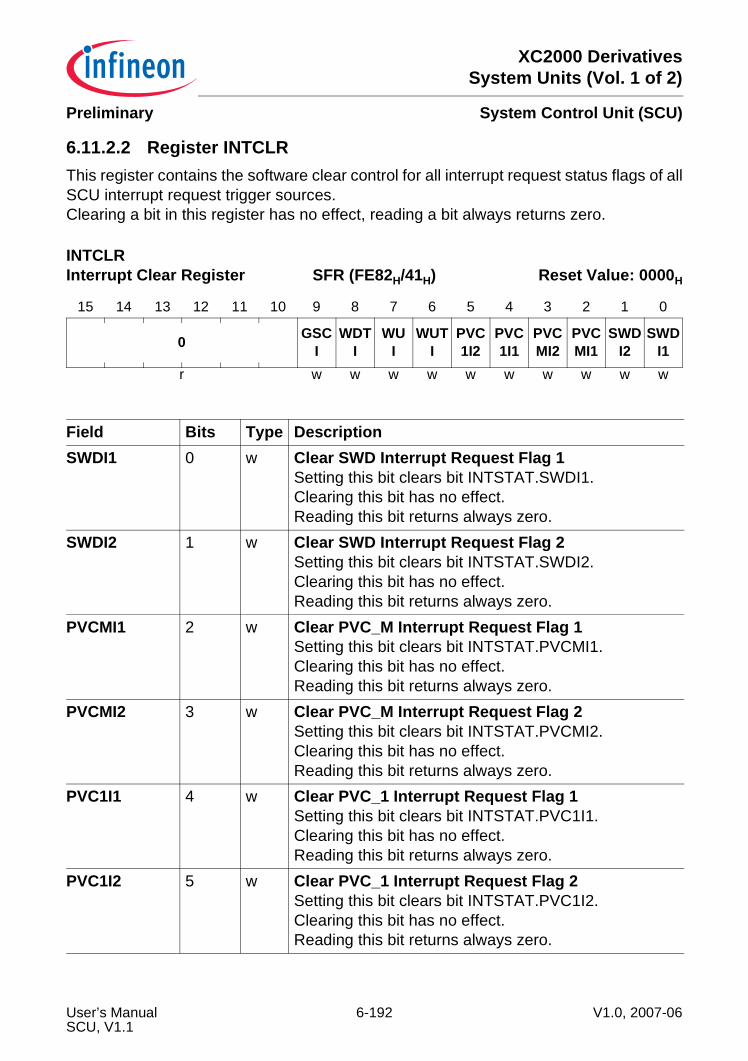
XC2000 DerivativesSystem Units (Vol. 1 of 2)
System Control Unit (SCU)Preliminary
6.11.2.2 Register INTCLRThis register contains the software clear control for all interrupt request status flags of allSCU interrupt request trigger sources.Clearing a bit in this register has no effect, reading a bit always returns zero.
INTCLRInterrupt Clear Register SFR (FE82H/41H) Reset Value: 0000H
15 14 13 12 11 10 9 8 7 6 5 4 3 2 1 0
0 GSCI
WDTI
WUI
WUTI
PVC1I2
PVC1I1
PVCMI2
PVCMI1
SWDI2
SWDI1
r w w w w w w w w w w
Field Bits Type DescriptionSWDI1 0 w Clear SWD Interrupt Request Flag 1
Setting this bit clears bit INTSTAT.SWDI1.Clearing this bit has no effect.Reading this bit returns always zero.
SWDI2 1 w Clear SWD Interrupt Request Flag 2Setting this bit clears bit INTSTAT.SWDI2.Clearing this bit has no effect.Reading this bit returns always zero.
PVCMI1 2 w Clear PVC_M Interrupt Request Flag 1Setting this bit clears bit INTSTAT.PVCMI1.Clearing this bit has no effect.Reading this bit returns always zero.
PVCMI2 3 w Clear PVC_M Interrupt Request Flag 2Setting this bit clears bit INTSTAT.PVCMI2.Clearing this bit has no effect.Reading this bit returns always zero.
PVC1I1 4 w Clear PVC_1 Interrupt Request Flag 1Setting this bit clears bit INTSTAT.PVC1I1.Clearing this bit has no effect.Reading this bit returns always zero.
PVC1I2 5 w Clear PVC_1 Interrupt Request Flag 2Setting this bit clears bit INTSTAT.PVC1I2.Clearing this bit has no effect.Reading this bit returns always zero.
User’s Manual 6-192 V1.0, 2007-06SCU, V1.1
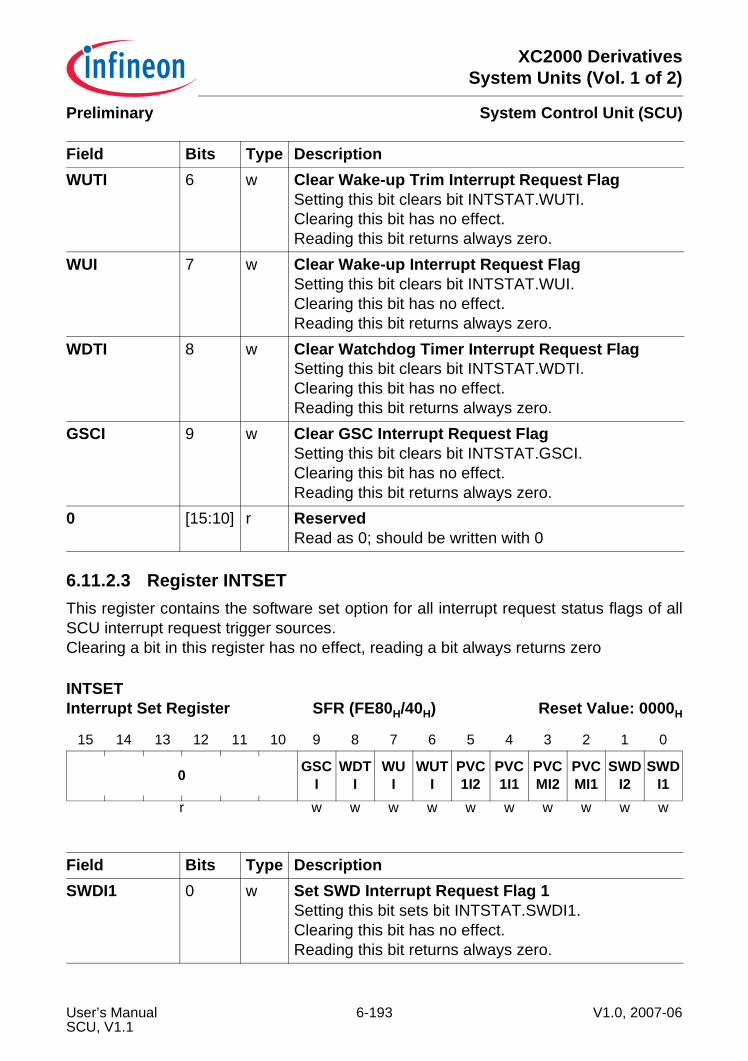
XC2000 DerivativesSystem Units (Vol. 1 of 2)
System Control Unit (SCU)Preliminary
6.11.2.3 Register INTSETThis register contains the software set option for all interrupt request status flags of allSCU interrupt request trigger sources.Clearing a bit in this register has no effect, reading a bit always returns zero
WUTI 6 w Clear Wake-up Trim Interrupt Request FlagSetting this bit clears bit INTSTAT.WUTI.Clearing this bit has no effect.Reading this bit returns always zero.
WUI 7 w Clear Wake-up Interrupt Request FlagSetting this bit clears bit INTSTAT.WUI.Clearing this bit has no effect.Reading this bit returns always zero.
WDTI 8 w Clear Watchdog Timer Interrupt Request FlagSetting this bit clears bit INTSTAT.WDTI.Clearing this bit has no effect.Reading this bit returns always zero.
GSCI 9 w Clear GSC Interrupt Request FlagSetting this bit clears bit INTSTAT.GSCI.Clearing this bit has no effect.Reading this bit returns always zero.
0 [15:10] r ReservedRead as 0; should be written with 0
INTSETInterrupt Set Register SFR (FE80H/40H) Reset Value: 0000H
15 14 13 12 11 10 9 8 7 6 5 4 3 2 1 0
0 GSCI
WDTI
WUI
WUTI
PVC1I2
PVC1I1
PVCMI2
PVCMI1
SWDI2
SWDI1
r w w w w w w w w w w
Field Bits Type DescriptionSWDI1 0 w Set SWD Interrupt Request Flag 1
Setting this bit sets bit INTSTAT.SWDI1.Clearing this bit has no effect.Reading this bit returns always zero.
Field Bits Type Description
User’s Manual 6-193 V1.0, 2007-06SCU, V1.1
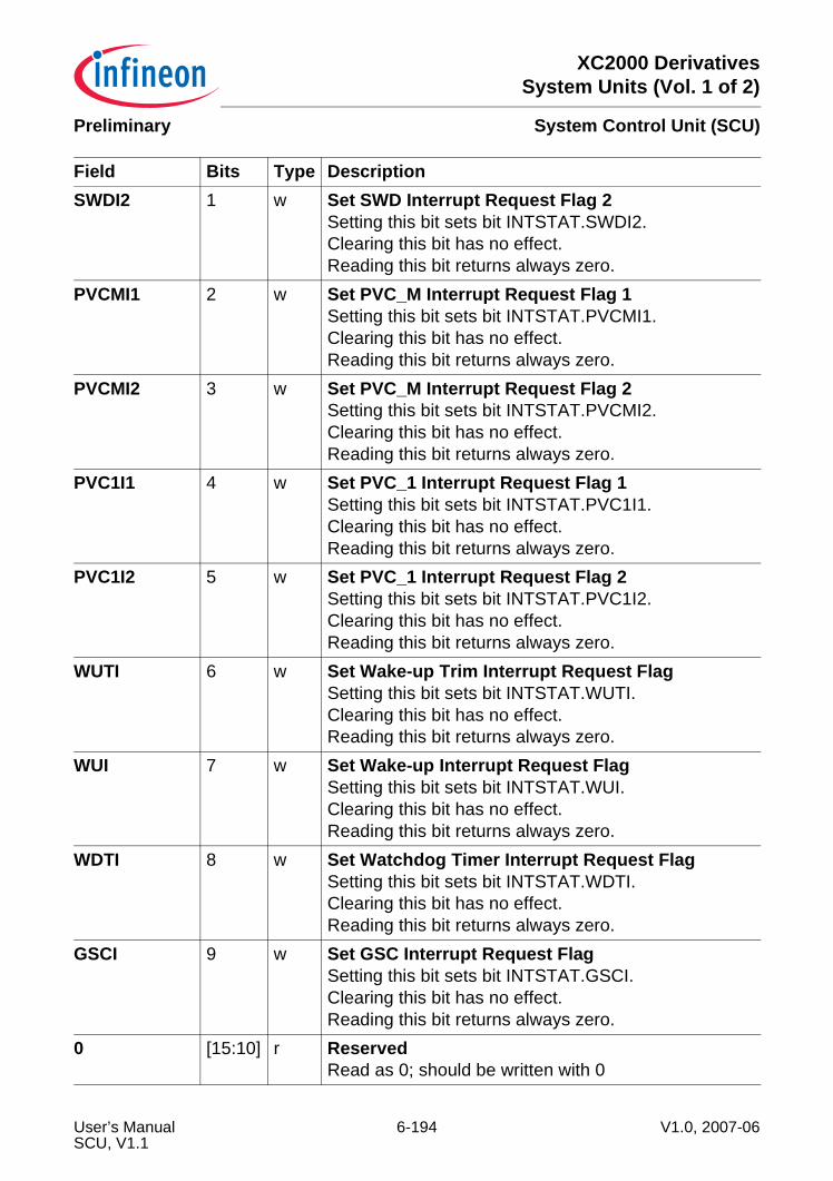
XC2000 DerivativesSystem Units (Vol. 1 of 2)
System Control Unit (SCU)Preliminary
SWDI2 1 w Set SWD Interrupt Request Flag 2Setting this bit sets bit INTSTAT.SWDI2.Clearing this bit has no effect.Reading this bit returns always zero.
PVCMI1 2 w Set PVC_M Interrupt Request Flag 1Setting this bit sets bit INTSTAT.PVCMI1.Clearing this bit has no effect.Reading this bit returns always zero.
PVCMI2 3 w Set PVC_M Interrupt Request Flag 2Setting this bit sets bit INTSTAT.PVCMI2.Clearing this bit has no effect.Reading this bit returns always zero.
PVC1I1 4 w Set PVC_1 Interrupt Request Flag 1Setting this bit sets bit INTSTAT.PVC1I1.Clearing this bit has no effect.Reading this bit returns always zero.
PVC1I2 5 w Set PVC_1 Interrupt Request Flag 2Setting this bit sets bit INTSTAT.PVC1I2.Clearing this bit has no effect.Reading this bit returns always zero.
WUTI 6 w Set Wake-up Trim Interrupt Request FlagSetting this bit sets bit INTSTAT.WUTI.Clearing this bit has no effect.Reading this bit returns always zero.
WUI 7 w Set Wake-up Interrupt Request FlagSetting this bit sets bit INTSTAT.WUI.Clearing this bit has no effect.Reading this bit returns always zero.
WDTI 8 w Set Watchdog Timer Interrupt Request FlagSetting this bit sets bit INTSTAT.WDTI.Clearing this bit has no effect.Reading this bit returns always zero.
GSCI 9 w Set GSC Interrupt Request FlagSetting this bit sets bit INTSTAT.GSCI.Clearing this bit has no effect.Reading this bit returns always zero.
0 [15:10] r ReservedRead as 0; should be written with 0
Field Bits Type Description
User’s Manual 6-194 V1.0, 2007-06SCU, V1.1
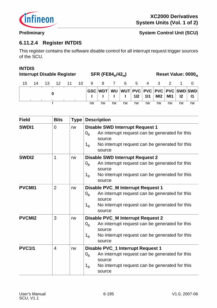
XC2000 DerivativesSystem Units (Vol. 1 of 2)
System Control Unit (SCU)Preliminary
6.11.2.4 Register INTDISThis register contains the software disable control for all interrupt request trigger sourcesof the SCU.
INTDISInterrupt Disable Register SFR (FE84H/42H) Reset Value: 0000H
15 14 13 12 11 10 9 8 7 6 5 4 3 2 1 0
0 GSCI
WDTI
WUI
WUTI
PVC1I2
PVC1I1
PVCMI2
PVCMI1
SWDI2
SWDI1
r rw rw rw rw rw rw rw rw rw rw
Field Bits Type DescriptionSWDI1 0 rw Disable SWD Interrupt Request 1
0B An interrupt request can be generated for this source
1B No interrupt request can be generated for this source
SWDI2 1 rw Disable SWD Interrupt Request 20B An interrupt request can be generated for this
source1B No interrupt request can be generated for this
sourcePVCMI1 2 rw Disable PVC_M Interrupt Request 1
0B An interrupt request can be generated for this source
1B No interrupt request can be generated for this source
PVCMI2 3 rw Disable PVC_M Interrupt Request 20B An interrupt request can be generated for this
source1B No interrupt request can be generated for this
sourcePVC1I1 4 rw Disable PVC_1 Interrupt Request 1
0B An interrupt request can be generated for this source
1B No interrupt request can be generated for this source
User’s Manual 6-195 V1.0, 2007-06SCU, V1.1
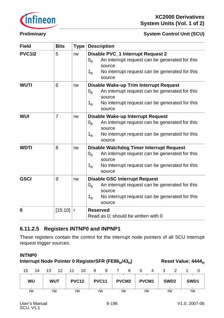
XC2000 DerivativesSystem Units (Vol. 1 of 2)
System Control Unit (SCU)Preliminary
6.11.2.5 Registers INTNP0 and INPNP1These registers contain the control for the interrupt node pointers of all SCU interruptrequest trigger sources.
PVC1I2 5 rw Disable PVC_1 Interrupt Request 20B An interrupt request can be generated for this
source1B No interrupt request can be generated for this
sourceWUTI 6 rw Disable Wake-up Trim Interrupt Request
0B An interrupt request can be generated for this source
1B No interrupt request can be generated for this source
WUI 7 rw Disable Wake-up Interrupt Request0B An interrupt request can be generated for this
source1B No interrupt request can be generated for this
sourceWDTI 8 rw Disable Watchdog Timer Interrupt Request
0B An interrupt request can be generated for this source
1B No interrupt request can be generated for this source
GSCI 9 rw Disable GSC Interrupt Request0B An interrupt request can be generated for this
source1B No interrupt request can be generated for this
source0 [15:10] r Reserved
Read as 0; should be written with 0
INTNP0Interrupt Node Pointer 0 RegisterSFR (FE86H/43H) Reset Value: 4444H
15 14 13 12 11 10 9 8 7 6 5 4 3 2 1 0
WU WUT PVC12 PVC11 PVCM2 PVCM1 SWD2 SWD1
rw rw rw rw rw rw rw rw
Field Bits Type Description
User’s Manual 6-196 V1.0, 2007-06SCU, V1.1
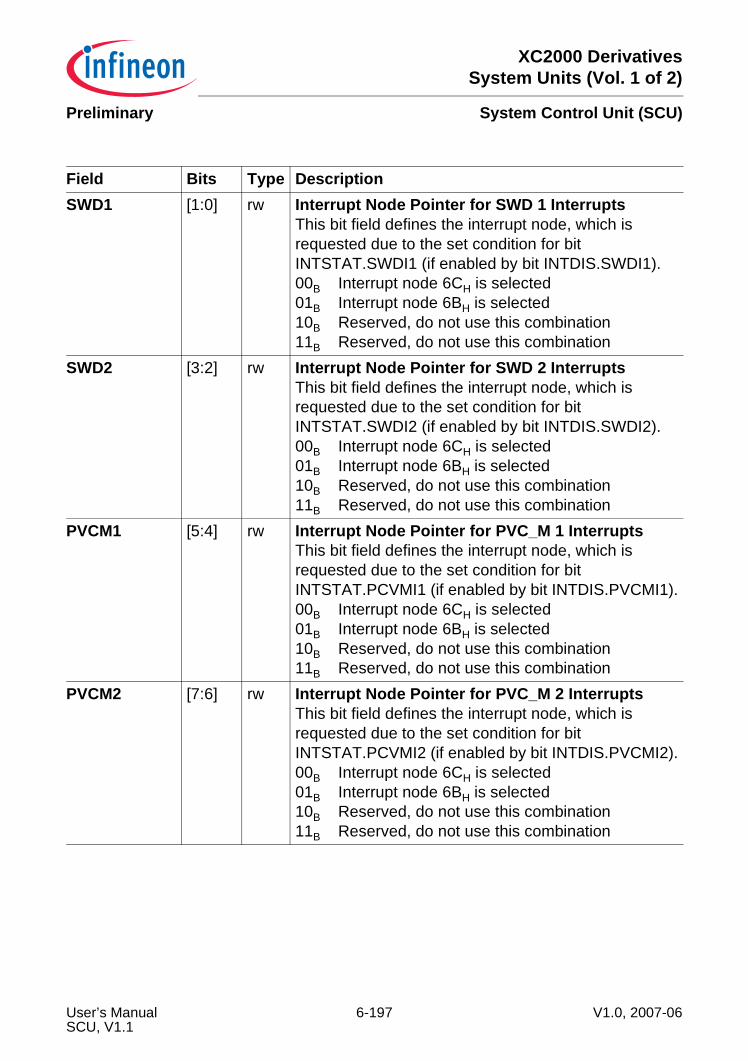
XC2000 DerivativesSystem Units (Vol. 1 of 2)
System Control Unit (SCU)Preliminary
Field Bits Type DescriptionSWD1 [1:0] rw Interrupt Node Pointer for SWD 1 Interrupts
This bit field defines the interrupt node, which is requested due to the set condition for bit INTSTAT.SWDI1 (if enabled by bit INTDIS.SWDI1).00B Interrupt node 6CH is selected01B Interrupt node 6BH is selected10B Reserved, do not use this combination11B Reserved, do not use this combination
SWD2 [3:2] rw Interrupt Node Pointer for SWD 2 InterruptsThis bit field defines the interrupt node, which is requested due to the set condition for bit INTSTAT.SWDI2 (if enabled by bit INTDIS.SWDI2).00B Interrupt node 6CH is selected01B Interrupt node 6BH is selected10B Reserved, do not use this combination11B Reserved, do not use this combination
PVCM1 [5:4] rw Interrupt Node Pointer for PVC_M 1 InterruptsThis bit field defines the interrupt node, which is requested due to the set condition for bit INTSTAT.PCVMI1 (if enabled by bit INTDIS.PVCMI1).00B Interrupt node 6CH is selected01B Interrupt node 6BH is selected10B Reserved, do not use this combination11B Reserved, do not use this combination
PVCM2 [7:6] rw Interrupt Node Pointer for PVC_M 2 InterruptsThis bit field defines the interrupt node, which is requested due to the set condition for bit INTSTAT.PCVMI2 (if enabled by bit INTDIS.PVCMI2).00B Interrupt node 6CH is selected01B Interrupt node 6BH is selected10B Reserved, do not use this combination11B Reserved, do not use this combination
User’s Manual 6-197 V1.0, 2007-06SCU, V1.1
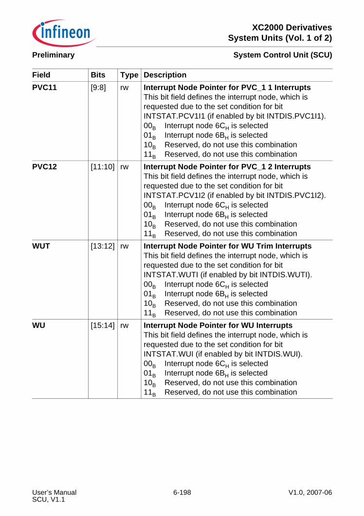
XC2000 DerivativesSystem Units (Vol. 1 of 2)
System Control Unit (SCU)Preliminary
PVC11 [9:8] rw Interrupt Node Pointer for PVC_1 1 InterruptsThis bit field defines the interrupt node, which is requested due to the set condition for bit INTSTAT.PCV1I1 (if enabled by bit INTDIS.PVC1I1).00B Interrupt node 6CH is selected01B Interrupt node 6BH is selected10B Reserved, do not use this combination11B Reserved, do not use this combination
PVC12 [11:10] rw Interrupt Node Pointer for PVC_1 2 InterruptsThis bit field defines the interrupt node, which is requested due to the set condition for bit INTSTAT.PCV1I2 (if enabled by bit INTDIS.PVC1I2).00B Interrupt node 6CH is selected01B Interrupt node 6BH is selected10B Reserved, do not use this combination11B Reserved, do not use this combination
WUT [13:12] rw Interrupt Node Pointer for WU Trim InterruptsThis bit field defines the interrupt node, which is requested due to the set condition for bit INTSTAT.WUTI (if enabled by bit INTDIS.WUTI).00B Interrupt node 6CH is selected01B Interrupt node 6BH is selected10B Reserved, do not use this combination11B Reserved, do not use this combination
WU [15:14] rw Interrupt Node Pointer for WU InterruptsThis bit field defines the interrupt node, which is requested due to the set condition for bit INTSTAT.WUI (if enabled by bit INTDIS.WUI).00B Interrupt node 6CH is selected01B Interrupt node 6BH is selected10B Reserved, do not use this combination11B Reserved, do not use this combination
Field Bits Type Description
User’s Manual 6-198 V1.0, 2007-06SCU, V1.1
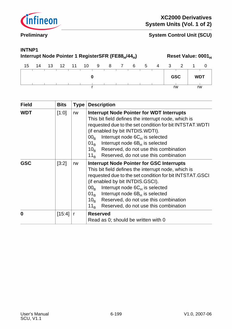
XC2000 DerivativesSystem Units (Vol. 1 of 2)
System Control Unit (SCU)Preliminary
INTNP1Interrupt Node Pointer 1 RegisterSFR (FE88H/44H) Reset Value: 0001H
15 14 13 12 11 10 9 8 7 6 5 4 3 2 1 0
0 GSC WDT
r rw rw
Field Bits Type DescriptionWDT [1:0] rw Interrupt Node Pointer for WDT Interrupts
This bit field defines the interrupt node, which is requested due to the set condition for bit INTSTAT.WDTI (if enabled by bit INTDIS.WDTI).00B Interrupt node 6CH is selected01B Interrupt node 6BH is selected10B Reserved, do not use this combination11B Reserved, do not use this combination
GSC [3:2] rw Interrupt Node Pointer for GSC InterruptsThis bit field defines the interrupt node, which is requested due to the set condition for bit INTSTAT.GSCI (if enabled by bit INTDIS.GSCI).00B Interrupt node 6CH is selected01B Interrupt node 6BH is selected10B Reserved, do not use this combination11B Reserved, do not use this combination
0 [15:4] r ReservedRead as 0; should be written with 0
User’s Manual 6-199 V1.0, 2007-06SCU, V1.1
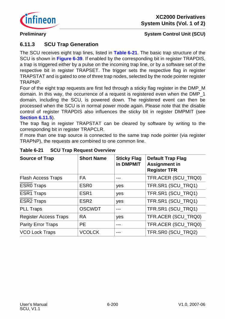
XC2000 DerivativesSystem Units (Vol. 1 of 2)
System Control Unit (SCU)Preliminary
6.11.3 SCU Trap GenerationThe SCU receives eight trap lines, listed in Table 6-21. The basic trap structure of theSCU is shown in Figure 6-39. If enabled by the corresponding bit in register TRAPDIS,a trap is triggered either by a pulse on the incoming trap line, or by a software set of therespective bit in register TRAPSET. The trigger sets the respective flag in registerTRAPSTAT and is gated to one of three trap nodes, selected by the node pointer registerTRAPNP.Four of the eight trap requests are first fed through a sticky flag register in the DMP_Mdomain. In this way, the occurrence of a request is registered even when the DMP_1domain, including the SCU, is powered down. The registered event can then beprocessed when the SCU is in normal power mode again. Please note that the disablecontrol of register TRAPDIS also influences the sticky bit in register DMPMIT (seeSection 6.11.5).The trap flag in register TRAPSTAT can be cleared by software by writing to thecorresponding bit in register TRAPCLR.If more than one trap source is connected to the same trap node pointer (via registerTRAPNP), the requests are combined to one common line.
Table 6-21 SCU Trap Request OverviewSource of Trap Short Name Sticky Flag
in DMPMITDefault Trap Flag Assignment in Register TFR
Flash Access Traps FA --- TFR.ACER (SCU_TRQ0)ESR0 Traps ESR0 yes TFR.SR1 (SCU_TRQ1)ESR1 Traps ESR1 yes TFR.SR1 (SCU_TRQ1)ESR2 Traps ESR2 yes TFR.SR1 (SCU_TRQ1)PLL Traps OSCWDT --- TFR.SR1 (SCU_TRQ1)Register Access Traps RA yes TFR.ACER (SCU_TRQ0)Parity Error Traps PE --- TFR.ACER (SCU_TRQ0)VCO Lock Traps VCOLCK --- TFR.SR0 (SCU_TRQ2)
User’s Manual 6-200 V1.0, 2007-06SCU, V1.1
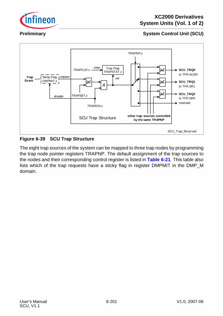
XC2000 DerivativesSystem Units (Vol. 1 of 2)
System Control Unit (SCU)Preliminary
Figure 6-39 SCU Trap Structure
The eight trap sources of the system can be mapped to three trap nodes by programmingthe trap node pointer registers TRAPNP. The default assignment of the trap sources tothe nodes and their corresponding control register is listed in Table 6-21. This table alsolists which of the trap requests have a sticky flag in register DMPMIT in the DMP_Mdomain.
SCU_Trap_Struct.vsd
TRAPSET.x
SCU Trap Structure
clear
other trap sources controlledby the same TRAPNP
&
1
1
1
1
Trap FlagTRAPSTAT.x
TRAPDIS.x
TRAPCLR.x
setTrapEvent
TRAPNP.y
Sticky FlagDMPMIT.x
reserved
SCU_TRQ0
SCU_TRQ1
SCU_TRQ2
to TFR.ACER
to TFR.SR1
to TFR.SR0disable
request
User’s Manual 6-201 V1.0, 2007-06SCU, V1.1
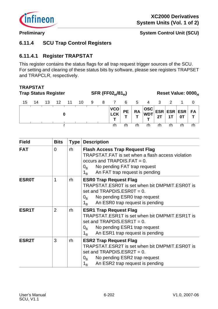
XC2000 DerivativesSystem Units (Vol. 1 of 2)
System Control Unit (SCU)Preliminary
6.11.4 SCU Trap Control Registers
6.11.4.1 Register TRAPSTATThis register contains the status flags for all trap request trigger sources of the SCU.For setting and clearing of these status bits by software, please see registers TRAPSETand TRAPCLR, respectively.
TRAPSTATTrap Status Register SFR (FF02H/81H) Reset Value: 0000H
15 14 13 12 11 10 9 8 7 6 5 4 3 2 1 0
0VCOLCK
T
PET
RAT
OSCWDT
T
ESR2T
ESR1T
ESR0T
FAT
r rh rh rh rh rh rh rh rh
Field Bits Type DescriptionFAT 0 rh Flash Access Trap Request Flag
TRAPSTAT.FAT is set when a flash access violation occurs and TRAPDIS.FAT = 0.0B No pending FAT trap request1B An FAT trap request is pending
ESR0T 1 rh ESR0 Trap Request FlagTRAPSTAT.ESR0T is set when bit DMPMIT.ESR0T is set and TRAPDIS.ESR0T = 0.0B No pending ESR0 trap request1B An ESR0 trap request is pending
ESR1T 2 rh ESR1 Trap Request FlagTRAPSTAT.ESR1T is set when bit DMPMIT.ESR1T is set and TRAPDIS.ESR1T = 0.0B No pending ESR1 trap request1B An ESR1 trap request is pending
ESR2T 3 rh ESR2 Trap Request FlagTRAPSTAT.ESR2T is set when bit DMPMIT.ESR0T is set and TRAPDIS.ESR2T = 0.0B No pending ESR2 trap request1B An ESR2 trap request is pending
User’s Manual 6-202 V1.0, 2007-06SCU, V1.1
XC2000 DerivativesSystem Units (Vol. 1 of 2)
System Control Unit (SCU)Preliminary
OSCWDTT 4 rh OSCWDT Trap Request FlagTRAPSTAT.OSCWDTT is set when an OSCWDT emergency event occurs and TRAPDIS.OSCWDTT = 0.0B No pending OSCWDT trap request1B An OSCWDT trap request is pending
RAT 5 rh Register Access Trap Request FlagTRAPSTAT.RAT is set when bit DMPMIT.RAT is set and TRAPDIS.RAT = 0.0B No pending RAT trap request1B An RAT trap request is pending
PET 6 rh Parity Error Trap Request FlagTRAPSTAT.PET is set when a memory parity error occurs and TRAPDIS.PET = 0.0B No pending PET trap request1B An PET trap request is pending
VCOLCKT 7 rh VCOWDT Trap Request FlagTRAPSTAT.VCOLCKT is set when a VCOLCK emergency event occurs and TRAPDIS.VCOLCKT = 0.0B No pending VCOLCK trap request1B An VCOLCK trap request is pending
0 [15:8] r ReservedRead as 0; should be written with 0.
Field Bits Type Description
User’s Manual 6-203 V1.0, 2007-06SCU, V1.1
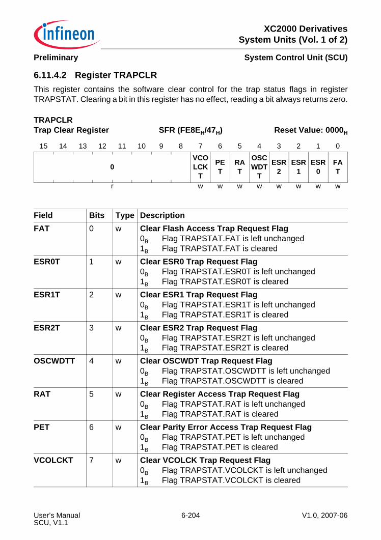
XC2000 DerivativesSystem Units (Vol. 1 of 2)
System Control Unit (SCU)Preliminary
6.11.4.2 Register TRAPCLRThis register contains the software clear control for the trap status flags in registerTRAPSTAT. Clearing a bit in this register has no effect, reading a bit always returns zero.
TRAPCLRTrap Clear Register SFR (FE8EH/47H) Reset Value: 0000H
15 14 13 12 11 10 9 8 7 6 5 4 3 2 1 0
0VCOLCK
T
PET
RAT
OSCWDT
T
ESR2
ESR1
ESR0
FAT
r w w w w w w w w
Field Bits Type DescriptionFAT 0 w Clear Flash Access Trap Request Flag
0B Flag TRAPSTAT.FAT is left unchanged1B Flag TRAPSTAT.FAT is cleared
ESR0T 1 w Clear ESR0 Trap Request Flag0B Flag TRAPSTAT.ESR0T is left unchanged1B Flag TRAPSTAT.ESR0T is cleared
ESR1T 2 w Clear ESR1 Trap Request Flag0B Flag TRAPSTAT.ESR1T is left unchanged1B Flag TRAPSTAT.ESR1T is cleared
ESR2T 3 w Clear ESR2 Trap Request Flag0B Flag TRAPSTAT.ESR2T is left unchanged1B Flag TRAPSTAT.ESR2T is cleared
OSCWDTT 4 w Clear OSCWDT Trap Request Flag0B Flag TRAPSTAT.OSCWDTT is left unchanged1B Flag TRAPSTAT.OSCWDTT is cleared
RAT 5 w Clear Register Access Trap Request Flag0B Flag TRAPSTAT.RAT is left unchanged1B Flag TRAPSTAT.RAT is cleared
PET 6 w Clear Parity Error Access Trap Request Flag0B Flag TRAPSTAT.PET is left unchanged1B Flag TRAPSTAT.PET is cleared
VCOLCKT 7 w Clear VCOLCK Trap Request Flag0B Flag TRAPSTAT.VCOLCKT is left unchanged1B Flag TRAPSTAT.VCOLCKT is cleared
User’s Manual 6-204 V1.0, 2007-06SCU, V1.1
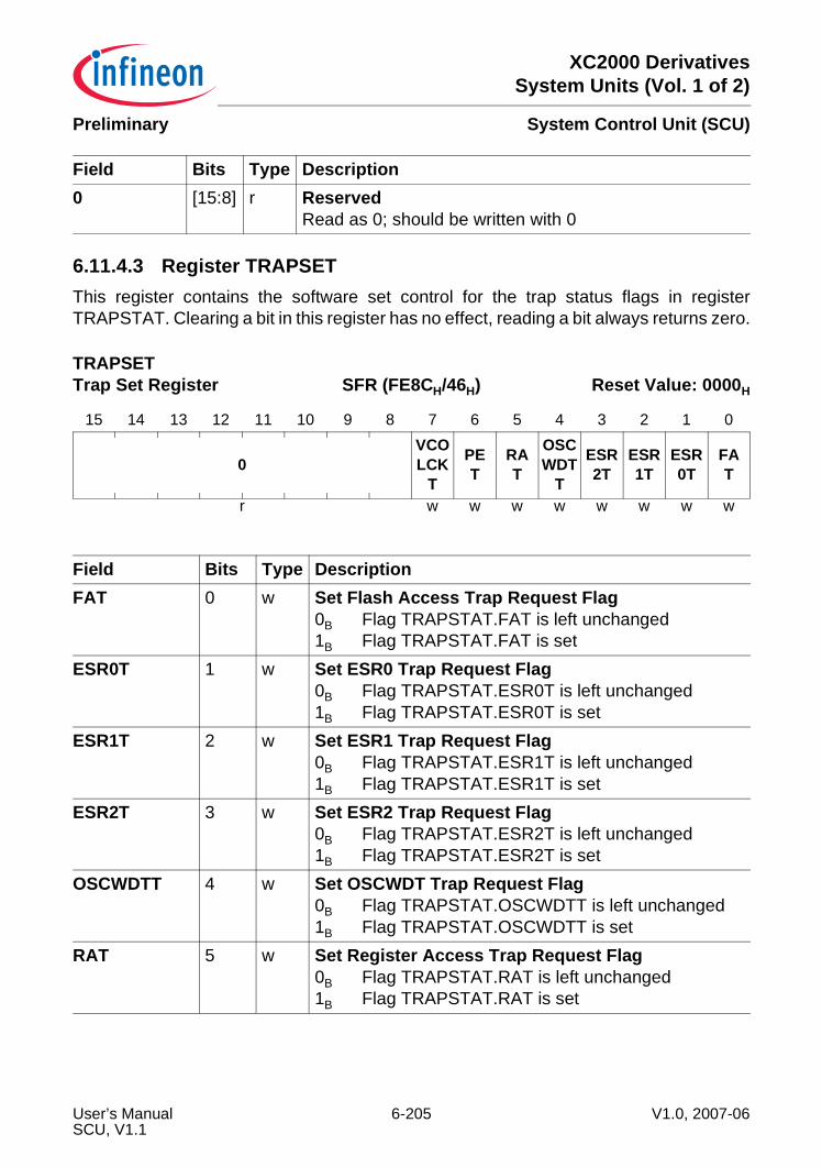
XC2000 DerivativesSystem Units (Vol. 1 of 2)
System Control Unit (SCU)Preliminary
6.11.4.3 Register TRAPSETThis register contains the software set control for the trap status flags in registerTRAPSTAT. Clearing a bit in this register has no effect, reading a bit always returns zero.
0 [15:8] r ReservedRead as 0; should be written with 0
TRAPSETTrap Set Register SFR (FE8CH/46H) Reset Value: 0000H
15 14 13 12 11 10 9 8 7 6 5 4 3 2 1 0
0VCOLCK
T
PET
RAT
OSCWDT
T
ESR2T
ESR1T
ESR0T
FAT
r w w w w w w w w
Field Bits Type DescriptionFAT 0 w Set Flash Access Trap Request Flag
0B Flag TRAPSTAT.FAT is left unchanged1B Flag TRAPSTAT.FAT is set
ESR0T 1 w Set ESR0 Trap Request Flag0B Flag TRAPSTAT.ESR0T is left unchanged1B Flag TRAPSTAT.ESR0T is set
ESR1T 2 w Set ESR1 Trap Request Flag0B Flag TRAPSTAT.ESR1T is left unchanged1B Flag TRAPSTAT.ESR1T is set
ESR2T 3 w Set ESR2 Trap Request Flag0B Flag TRAPSTAT.ESR2T is left unchanged1B Flag TRAPSTAT.ESR2T is set
OSCWDTT 4 w Set OSCWDT Trap Request Flag0B Flag TRAPSTAT.OSCWDTT is left unchanged1B Flag TRAPSTAT.OSCWDTT is set
RAT 5 w Set Register Access Trap Request Flag0B Flag TRAPSTAT.RAT is left unchanged1B Flag TRAPSTAT.RAT is set
Field Bits Type Description
User’s Manual 6-205 V1.0, 2007-06SCU, V1.1
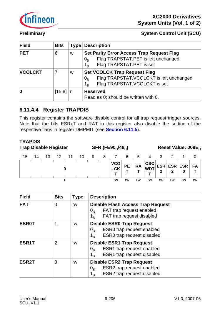
XC2000 DerivativesSystem Units (Vol. 1 of 2)
System Control Unit (SCU)Preliminary
6.11.4.4 Register TRAPDISThis register contains the software disable control for all trap request trigger sources.Note that the bits ESRxT and RAT in this register also disable the setting of therespective flags in register DMPMIT (see Section 6.11.5).
PET 6 w Set Parity Error Access Trap Request Flag0B Flag TRAPSTAT.PET is left unchanged1B Flag TRAPSTAT.PET is set
VCOLCKT 7 w Set VCOLCK Trap Request Flag0B Flag TRAPSTAT.VCOLCKT is left unchanged1B Flag TRAPSTAT.VCOLCKT is set
0 [15:8] r ReservedRead as 0; should be written with 0.
TRAPDISTrap Disable Register SFR (FE90H/48H) Reset Value: 009EH
15 14 13 12 11 10 9 8 7 6 5 4 3 2 1 0
0VCOLCK
T
PET
RAT
OSCWDT
T
ESR2
ESR2
ESR0
FAT
r rw rw rw rw rw rw rw rw
Field Bits Type DescriptionFAT 0 rw Disable Flash Access Trap Request
0B FAT trap request enabled1B FAT trap request disabled
ESR0T 1 rw Disable ESR0 Trap Request0B ESR0 trap request enabled1B ESR0 trap request disabled
ESR1T 2 rw Disable ESR1 Trap Request0B ESR1 trap request enabled1B ESR1 trap request disabled
ESR2T 3 rw Disable ESR2 Trap Request0B ESR2 trap request enabled1B ESR2 trap request disabled
Field Bits Type Description
User’s Manual 6-206 V1.0, 2007-06SCU, V1.1
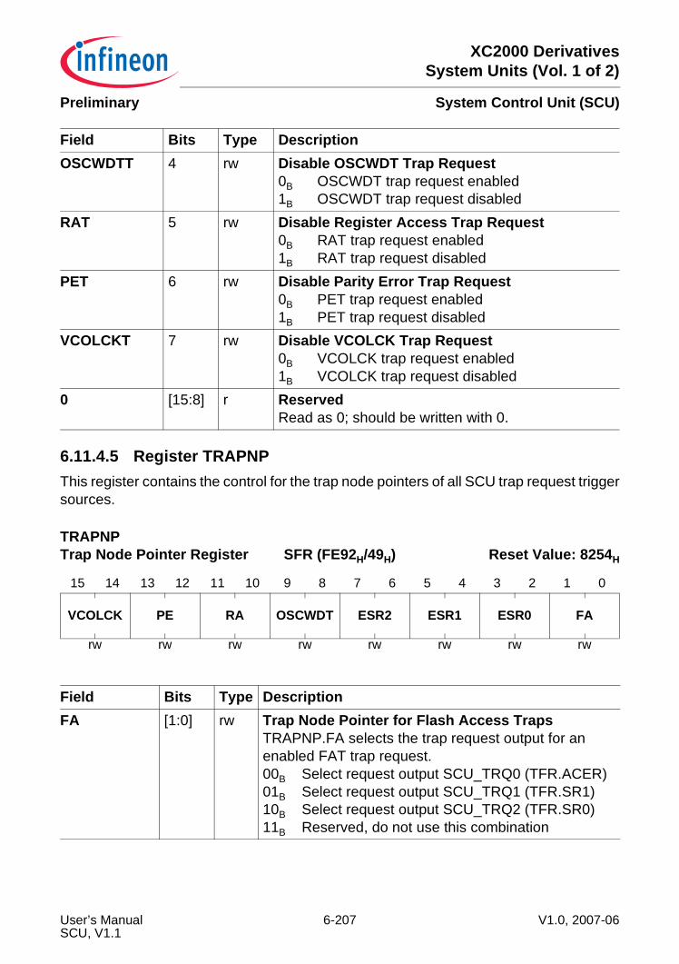
XC2000 DerivativesSystem Units (Vol. 1 of 2)
System Control Unit (SCU)Preliminary
6.11.4.5 Register TRAPNPThis register contains the control for the trap node pointers of all SCU trap request triggersources.
OSCWDTT 4 rw Disable OSCWDT Trap Request0B OSCWDT trap request enabled1B OSCWDT trap request disabled
RAT 5 rw Disable Register Access Trap Request0B RAT trap request enabled1B RAT trap request disabled
PET 6 rw Disable Parity Error Trap Request0B PET trap request enabled1B PET trap request disabled
VCOLCKT 7 rw Disable VCOLCK Trap Request0B VCOLCK trap request enabled1B VCOLCK trap request disabled
0 [15:8] r ReservedRead as 0; should be written with 0.
TRAPNPTrap Node Pointer Register SFR (FE92H/49H) Reset Value: 8254H
15 14 13 12 11 10 9 8 7 6 5 4 3 2 1 0
VCOLCK PE RA OSCWDT ESR2 ESR1 ESR0 FA
rw rw rw rw rw rw rw rw
Field Bits Type DescriptionFA [1:0] rw Trap Node Pointer for Flash Access Traps
TRAPNP.FA selects the trap request output for an enabled FAT trap request.00B Select request output SCU_TRQ0 (TFR.ACER)01B Select request output SCU_TRQ1 (TFR.SR1)10B Select request output SCU_TRQ2 (TFR.SR0)11B Reserved, do not use this combination
Field Bits Type Description
User’s Manual 6-207 V1.0, 2007-06SCU, V1.1
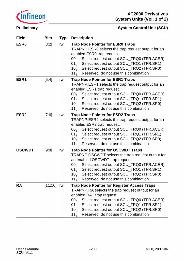
XC2000 DerivativesSystem Units (Vol. 1 of 2)
System Control Unit (SCU)Preliminary
ESR0 [3:2] rw Trap Node Pointer for ESR0 TrapsTRAPNP.ESR0 selects the trap request output for an enabled ESR0 trap request.00B Select request output SCU_TRQ0 (TFR.ACER)01B Select request output SCU_TRQ1 (TFR.SR1)10B Select request output SCU_TRQ2 (TFR.SR0)11B Reserved, do not use this combination
ESR1 [5:4] rw Trap Node Pointer for ESR1 TrapsTRAPNP.ESR1 selects the trap request output for an enabled ESR1 trap request.00B Select request output SCU_TRQ0 (TFR.ACER)01B Select request output SCU_TRQ1 (TFR.SR1)10B Select request output SCU_TRQ2 (TFR.SR0)11B Reserved, do not use this combination
ESR2 [7:6] rw Trap Node Pointer for ESR2 TrapsTRAPNP.ESR2 selects the trap request output for an enabled ESR2 trap request.00B Select request output SCU_TRQ0 (TFR.ACER)01B Select request output SCU_TRQ1 (TFR.SR1)10B Select request output SCU_TRQ2 (TFR.SR0)11B Reserved, do not use this combination
OSCWDT [9:8] rw Trap Node Pointer for OSCWDT TrapsTRAPNP.OSCWDT selects the trap request output for an enabled OSCWDT trap request.00B Select request output SCU_TRQ0 (TFR.ACER)01B Select request output SCU_TRQ1 (TFR.SR1)10B Select request output SCU_TRQ2 (TFR.SR0)11B Reserved, do not use this combination
RA [11:10] rw Trap Node Pointer for Register Access TrapsTRAPNP.RA selects the trap request output for an enabled RAT trap request.00B Select request output SCU_TRQ0 (TFR.ACER)01B Select request output SCU_TRQ1 (TFR.SR1)10B Select request output SCU_TRQ2 (TFR.SR0)11B Reserved, do not use this combination
Field Bits Type Description
User’s Manual 6-208 V1.0, 2007-06SCU, V1.1
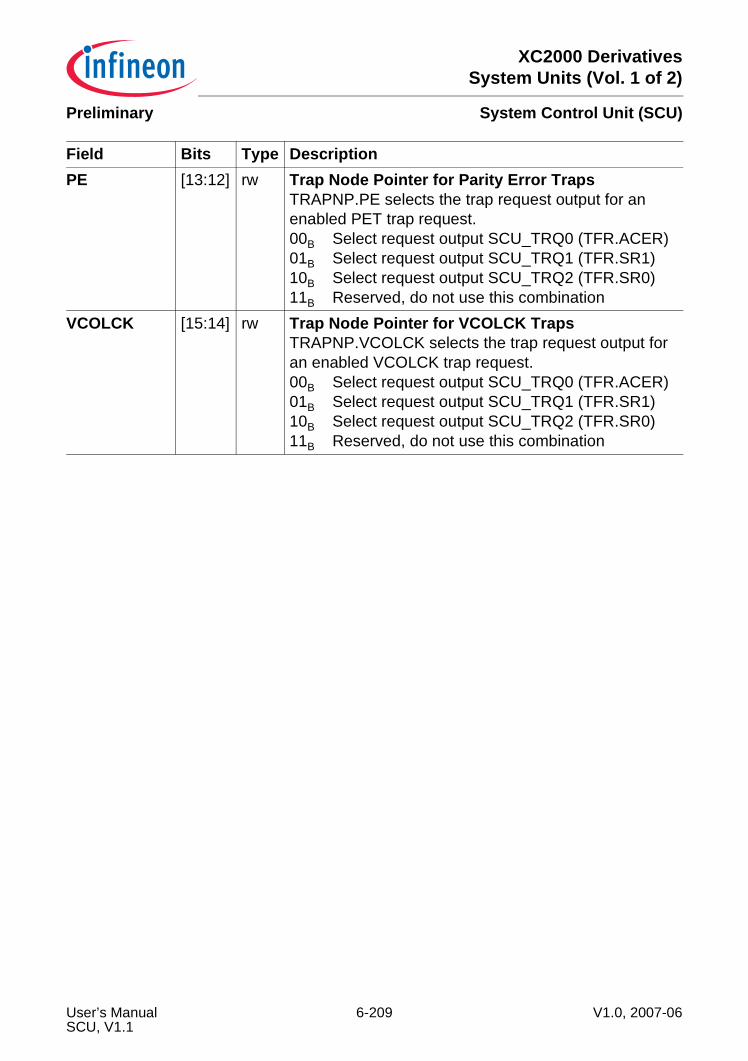
XC2000 DerivativesSystem Units (Vol. 1 of 2)
System Control Unit (SCU)Preliminary
PE [13:12] rw Trap Node Pointer for Parity Error TrapsTRAPNP.PE selects the trap request output for an enabled PET trap request.00B Select request output SCU_TRQ0 (TFR.ACER)01B Select request output SCU_TRQ1 (TFR.SR1)10B Select request output SCU_TRQ2 (TFR.SR0)11B Reserved, do not use this combination
VCOLCK [15:14] rw Trap Node Pointer for VCOLCK TrapsTRAPNP.VCOLCK selects the trap request output for an enabled VCOLCK trap request.00B Select request output SCU_TRQ0 (TFR.ACER)01B Select request output SCU_TRQ1 (TFR.SR1)10B Select request output SCU_TRQ2 (TFR.SR0)11B Reserved, do not use this combination
Field Bits Type Description
User’s Manual 6-209 V1.0, 2007-06SCU, V1.1

XC2000 DerivativesSystem Units (Vol. 1 of 2)
System Control Unit (SCU)Preliminary
6.11.5 DPM_M Interrupt and Trap SupportFor a number of SCU interrupt and trap requests, sticky status flags are implementedadditionally in the DMP_M. These flags are set with a trigger, and if set, trigger theinterrupt or trap generation in the DMP_1 SCU. In this way, no trap trigger is lost, evenwhen the DMP_1 is currently not powered. The flags are located in register DMPMIT.Please note that the disable control bits in registers INTDIS and TRAPDIS also controlthe setting of the respective DMPMIT.x flag, as illustrated in Figure 6-40.
Figure 6-40 DPM_M Sticky Interrupt and Trap FlagsSCU_DMPMIT_Struct.vsd
DMP_M
clear Interrupt / Trap TriggerFlag DMPMIT.xDMPMITCLR.x
setInterruptor Trap
Event
to SCUInterrupt/TrapStructure
&
INTDIS.xTRAPDIS.x
disable
request
User’s Manual 6-210 V1.0, 2007-06SCU, V1.1
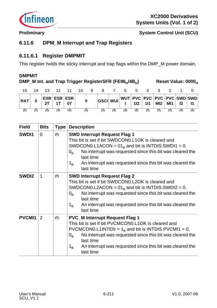
XC2000 DerivativesSystem Units (Vol. 1 of 2)
System Control Unit (SCU)Preliminary
6.11.6 DPM_M Interrupt and Trap Registers
6.11.6.1 Register DMPMITThis register holds the sticky interrupt and trap flags within the DMP_M power domain.
DMPMITDMP_M Int. and Trap Trigger RegisterSFR (FE96H/4BH) Reset Value: 0000H
15 14 13 12 11 10 9 8 7 6 5 4 3 2 1 0
RAT 0 ESR2T
ESR1T
ESR0T 0 GSCI WUI WUT
IPVC1I2
PVC1I1
PVCMI2
PVCMI1
SWDI2
SWDI1
rh rh rh rh rh rh rh rh rh rh rh rh rh rh rh
Field Bits Type DescriptionSWDI1 0 rh SWD Interrupt Request Flag 1
This bit is set if bit SWDCON0.L1OK is cleared and SWDCON0.L1ACON = 01B and bit is INTDIS.SWDI1 = 0.0B No interrupt was requested since this bit was cleared the
last time1B An interrupt was requested since this bit was cleared the
last timeSWDI2 1 rh SWD Interrupt Request Flag 2
This bit is set if bit SWDCON0.L2OK is cleared and SWDCON0.L2ACON = 01B and bit is INTDIS.SWDI2 = 0.0B No interrupt was requested since this bit was cleared the
last time1B An interrupt was requested since this bit was cleared the
last timePVCMI1 2 rh PVC_M Interrupt Request Flag 1
This bit is set if bit PVCMCON0.L1OK is cleared and PVCMCON0.L1INTEN = 1B and bit is INTDIS.PVCMI1 = 0.0B No interrupt was requested since this bit was cleared the
last time1B An interrupt was requested since this bit was cleared the
last time
User’s Manual 6-211 V1.0, 2007-06SCU, V1.1

XC2000 DerivativesSystem Units (Vol. 1 of 2)
System Control Unit (SCU)Preliminary
PVCMI2 3 rh PVC_M Interrupt Request Flag 2This bit is set if bit PVCMCON0.L2OK is cleared and PVCMCON0.L2INTEN = 1B and bit is INTDIS.PVCMI2 = 0.0B No interrupt was requested since this bit was cleared the
last time1B An interrupt was requested since this bit was cleared the
last timePVC1I1 4 rh PVC_1 Interrupt Request Flag 1
This bit is set if bit PVC1CON0.L1OK is cleared and PVC1CON0.L1INTEN = 1B and bit is INTDIS.PVC1I1 = 0.0B No interrupt was requested since this bit was cleared the
last time1B An interrupt was requested since this bit was cleared the
last timePVC1I2 5 rh PVC_1 Interrupt Request Flag 2
This bit is set if bit PVC1CON0.L2OK is cleared and PVC1CON0.L2INTEN = 1B and bit is INTDIS.PVC1I2 = 0.0B No interrupt was requested since this bit was cleared the
last time1B An interrupt was requested since this bit was cleared the
last timeWUTI 6 rh Wake-up Trim Interrupt Request Flag
This bit is set if a wake-up trim trigger occurs and bit is INTDIS.WUTI = 0.0B No interrupt was requested since this bit was cleared the
last time1B An interrupt was requested since this bit was cleared the
last timeWUI 7 rh Wake-up Interrupt Request Flag
This bit is set if a wake-up trigger occurs and bit is INTDIS.WUI = 0.0B No interrupt was requested since this bit was cleared the
last time1B An interrupt was requested since this bit was cleared the
last time
Field Bits Type Description
User’s Manual 6-212 V1.0, 2007-06SCU, V1.1

XC2000 DerivativesSystem Units (Vol. 1 of 2)
System Control Unit (SCU)Preliminary
GSCI 8 rh GSC Interrupt Request FlagThis bit is set if a GSC trigger occurs and bit is INTDIS.GSCI = 0.0B No interrupt was requested since this bit was cleared the
last time1B An interrupt was requested since this bit was cleared the
last timeESR0T 11 rh ESR0 Trap Request Flag
This bit is set if pin ESR0 is asserted.0B No trap was requested since this bit was cleared the last
time1B A trap was requested since this bit was cleared the last
timeESR1T 12 rh ESR1 Trap Request Flag
This bit is set if pin ESR1 is asserted.0B No trap was requested since this bit was cleared the last
time1B A trap was requested since this bit was cleared the last
timeESR2T 13 rh ESR2 Trap Request Flag
This bit is set if pin ESR2 is asserted.0B No trap was requested since this bit was cleared the last
time1B A trap was requested since this bit was cleared the last
timeRAT 15 rh Register Access Trap Request Flag
This bit is set a protected register is written by an non-authorized access.0B No trap was requested since this bit was cleared the last
time1B A trap was requested since this bit was cleared the last
time0 [10:9]
14rh Reserved
Read as 0; should be written with 0.
Field Bits Type Description
User’s Manual 6-213 V1.0, 2007-06SCU, V1.1
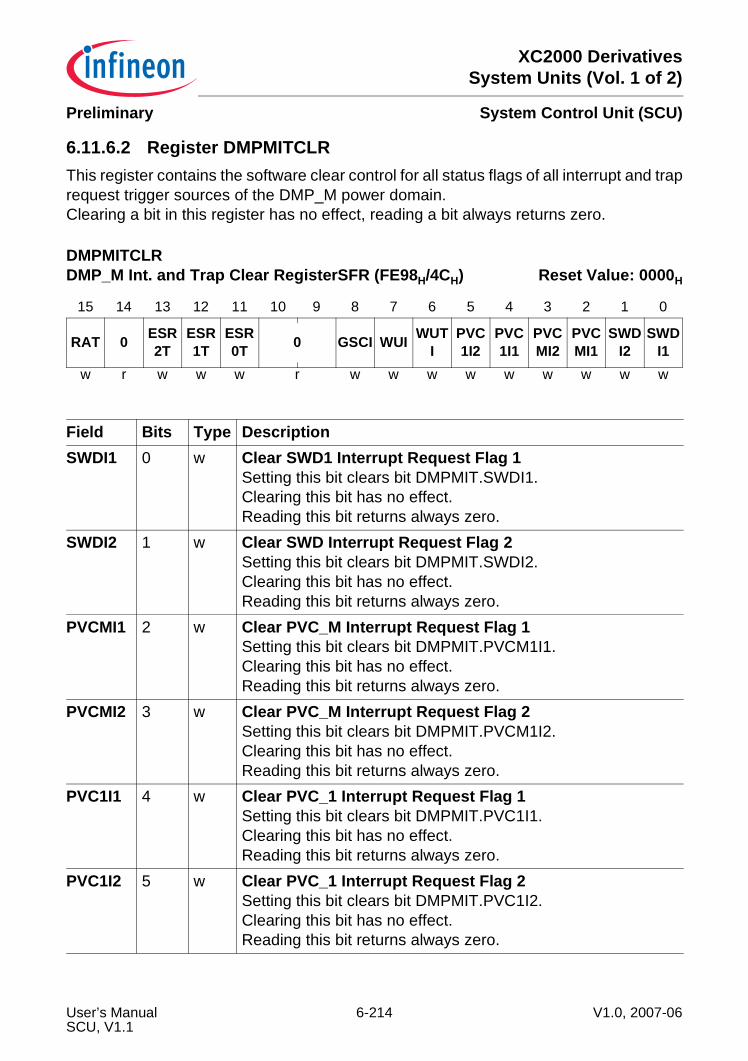
XC2000 DerivativesSystem Units (Vol. 1 of 2)
System Control Unit (SCU)Preliminary
6.11.6.2 Register DMPMITCLRThis register contains the software clear control for all status flags of all interrupt and traprequest trigger sources of the DMP_M power domain.Clearing a bit in this register has no effect, reading a bit always returns zero.
DMPMITCLRDMP_M Int. and Trap Clear RegisterSFR (FE98H/4CH) Reset Value: 0000H
15 14 13 12 11 10 9 8 7 6 5 4 3 2 1 0
RAT 0 ESR2T
ESR1T
ESR0T 0 GSCI WUI WUT
IPVC1I2
PVC1I1
PVCMI2
PVCMI1
SWDI2
SWDI1
w r w w w r w w w w w w w w w
Field Bits Type DescriptionSWDI1 0 w Clear SWD1 Interrupt Request Flag 1
Setting this bit clears bit DMPMIT.SWDI1.Clearing this bit has no effect.Reading this bit returns always zero.
SWDI2 1 w Clear SWD Interrupt Request Flag 2Setting this bit clears bit DMPMIT.SWDI2.Clearing this bit has no effect.Reading this bit returns always zero.
PVCMI1 2 w Clear PVC_M Interrupt Request Flag 1Setting this bit clears bit DMPMIT.PVCM1I1.Clearing this bit has no effect.Reading this bit returns always zero.
PVCMI2 3 w Clear PVC_M Interrupt Request Flag 2Setting this bit clears bit DMPMIT.PVCM1I2.Clearing this bit has no effect.Reading this bit returns always zero.
PVC1I1 4 w Clear PVC_1 Interrupt Request Flag 1Setting this bit clears bit DMPMIT.PVC1I1.Clearing this bit has no effect.Reading this bit returns always zero.
PVC1I2 5 w Clear PVC_1 Interrupt Request Flag 2Setting this bit clears bit DMPMIT.PVC1I2.Clearing this bit has no effect.Reading this bit returns always zero.
User’s Manual 6-214 V1.0, 2007-06SCU, V1.1
XC2000 DerivativesSystem Units (Vol. 1 of 2)
System Control Unit (SCU)Preliminary
WUTI 6 w Clear Wake-up Trim Interrupt Request FlagSetting this bit clears bit DMPMIT.WUTI.Clearing this bit has no effect.Reading this bit returns always zero.
WUI 7 w Clear Wake-up Interrupt Request FlagSetting this bit clears bit DMPMIT.WUI.Clearing this bit has no effect.Reading this bit returns always zero.
GSCI 8 w Clear GSC Interrupt Request FlagSetting this bit clears bit DMPMIT.GSCI.Clearing this bit has no effect.Reading this bit returns always zero.
ESR0T 11 w Clear ESR0 Trap Request FlagSetting this bit clears bit DMPMIT.ESR0T.Clearing this bit has no effect.Reading this bit returns always zero.
ESR1T 12 w Clear ESR1 Trap Request FlagSetting this bit clears bit DMPMIT.ESR1T.Clearing this bit has no effect.Reading this bit returns always zero.
ESR2T 13 w Clear ESR2 Trap Request FlagSetting this bit clears bit DMPMIT.ESR2T.Clearing this bit has no effect.Reading this bit returns always zero.
RAT 15 w Clear Register Access Trap Request FlagSetting this bit clears bit DMPMIT.RAT.Clearing this bit has no effect.Reading this bit returns always zero.
0 [10:9]14
r ReservedRead as 0; should be written with 0.
Field Bits Type Description
User’s Manual 6-215 V1.0, 2007-06SCU, V1.1
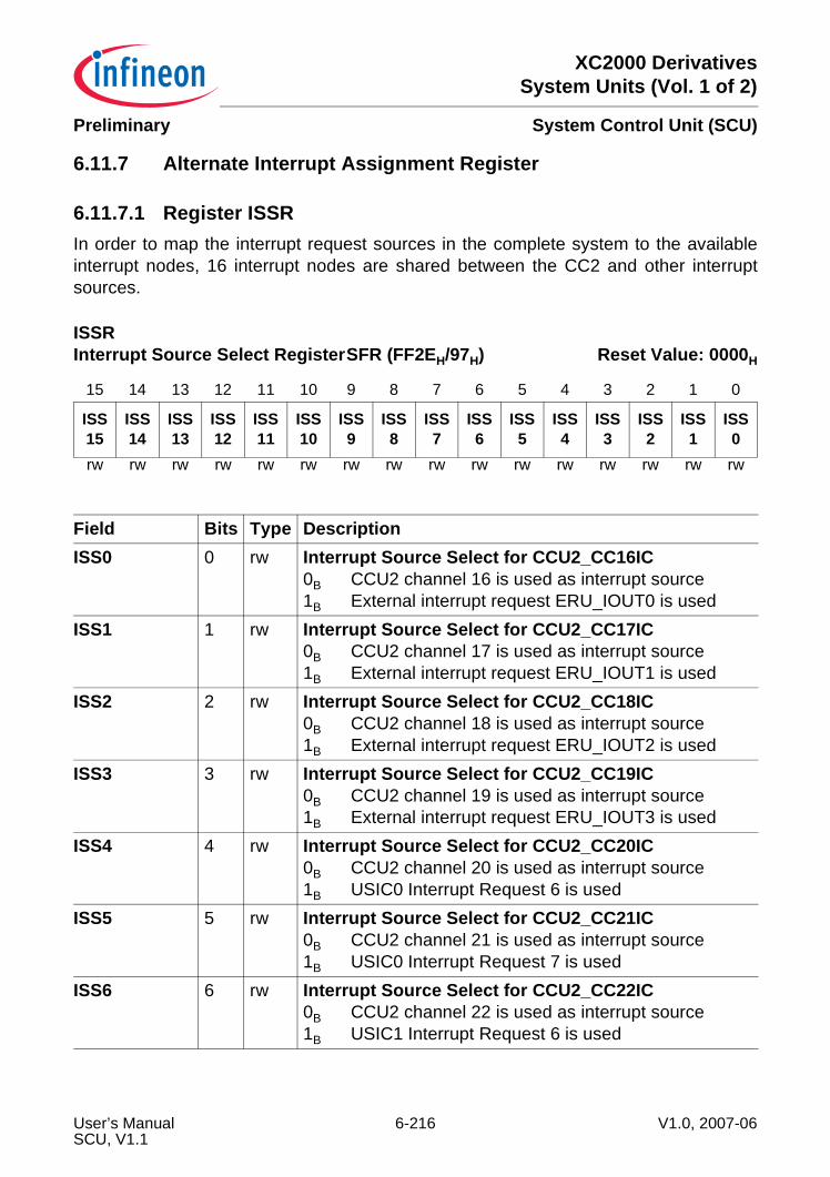
XC2000 DerivativesSystem Units (Vol. 1 of 2)
System Control Unit (SCU)Preliminary
6.11.7 Alternate Interrupt Assignment Register
6.11.7.1 Register ISSRIn order to map the interrupt request sources in the complete system to the availableinterrupt nodes, 16 interrupt nodes are shared between the CC2 and other interruptsources.
ISSRInterrupt Source Select RegisterSFR (FF2EH/97H) Reset Value: 0000H
15 14 13 12 11 10 9 8 7 6 5 4 3 2 1 0
ISS15
ISS14
ISS13
ISS12
ISS11
ISS10
ISS9
ISS8
ISS7
ISS6
ISS5
ISS4
ISS3
ISS2
ISS1
ISS0
rw rw rw rw rw rw rw rw rw rw rw rw rw rw rw rw
Field Bits Type DescriptionISS0 0 rw Interrupt Source Select for CCU2_CC16IC
0B CCU2 channel 16 is used as interrupt source1B External interrupt request ERU_IOUT0 is used
ISS1 1 rw Interrupt Source Select for CCU2_CC17IC0B CCU2 channel 17 is used as interrupt source1B External interrupt request ERU_IOUT1 is used
ISS2 2 rw Interrupt Source Select for CCU2_CC18IC0B CCU2 channel 18 is used as interrupt source1B External interrupt request ERU_IOUT2 is used
ISS3 3 rw Interrupt Source Select for CCU2_CC19IC0B CCU2 channel 19 is used as interrupt source1B External interrupt request ERU_IOUT3 is used
ISS4 4 rw Interrupt Source Select for CCU2_CC20IC0B CCU2 channel 20 is used as interrupt source1B USIC0 Interrupt Request 6 is used
ISS5 5 rw Interrupt Source Select for CCU2_CC21IC0B CCU2 channel 21 is used as interrupt source1B USIC0 Interrupt Request 7 is used
ISS6 6 rw Interrupt Source Select for CCU2_CC22IC0B CCU2 channel 22 is used as interrupt source1B USIC1 Interrupt Request 6 is used
User’s Manual 6-216 V1.0, 2007-06SCU, V1.1
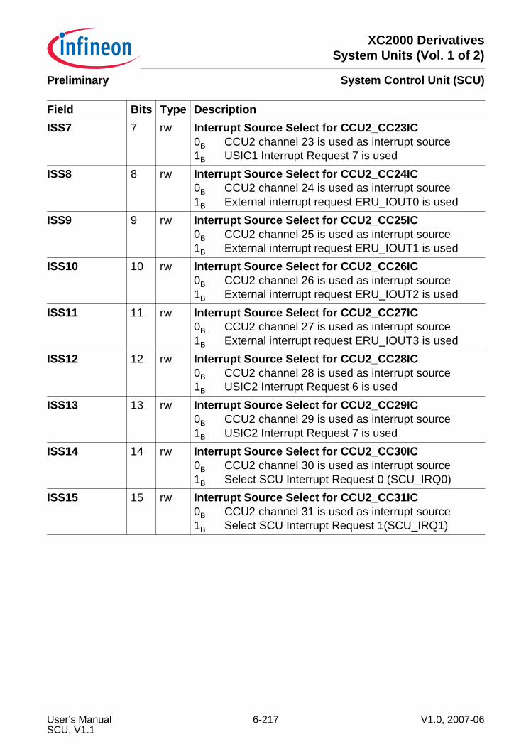
XC2000 DerivativesSystem Units (Vol. 1 of 2)
System Control Unit (SCU)Preliminary
ISS7 7 rw Interrupt Source Select for CCU2_CC23IC0B CCU2 channel 23 is used as interrupt source1B USIC1 Interrupt Request 7 is used
ISS8 8 rw Interrupt Source Select for CCU2_CC24IC0B CCU2 channel 24 is used as interrupt source1B External interrupt request ERU_IOUT0 is used
ISS9 9 rw Interrupt Source Select for CCU2_CC25IC0B CCU2 channel 25 is used as interrupt source1B External interrupt request ERU_IOUT1 is used
ISS10 10 rw Interrupt Source Select for CCU2_CC26IC0B CCU2 channel 26 is used as interrupt source1B External interrupt request ERU_IOUT2 is used
ISS11 11 rw Interrupt Source Select for CCU2_CC27IC0B CCU2 channel 27 is used as interrupt source1B External interrupt request ERU_IOUT3 is used
ISS12 12 rw Interrupt Source Select for CCU2_CC28IC0B CCU2 channel 28 is used as interrupt source1B USIC2 Interrupt Request 6 is used
ISS13 13 rw Interrupt Source Select for CCU2_CC29IC0B CCU2 channel 29 is used as interrupt source1B USIC2 Interrupt Request 7 is used
ISS14 14 rw Interrupt Source Select for CCU2_CC30IC0B CCU2 channel 30 is used as interrupt source1B Select SCU Interrupt Request 0 (SCU_IRQ0)
ISS15 15 rw Interrupt Source Select for CCU2_CC31IC0B CCU2 channel 31 is used as interrupt source1B Select SCU Interrupt Request 1(SCU_IRQ1)
Field Bits Type Description
User’s Manual 6-217 V1.0, 2007-06SCU, V1.1
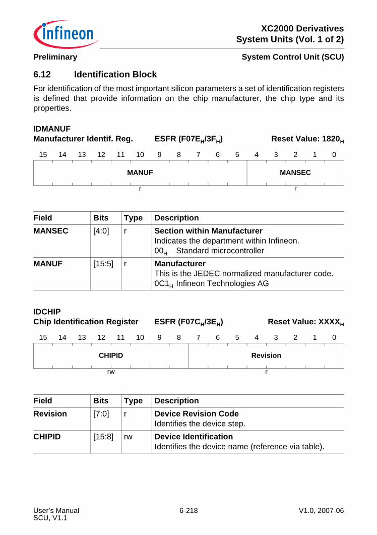
XC2000 DerivativesSystem Units (Vol. 1 of 2)
System Control Unit (SCU)Preliminary
6.12 Identification BlockFor identification of the most important silicon parameters a set of identification registersis defined that provide information on the chip manufacturer, the chip type and itsproperties.
IDMANUFManufacturer Identif. Reg. ESFR (F07EH/3FH) Reset Value: 1820H
15 14 13 12 11 10 9 8 7 6 5 4 3 2 1 0
MANUF MANSEC
r r
Field Bits Type DescriptionMANSEC [4:0] r Section within Manufacturer
Indicates the department within Infineon.00H Standard microcontroller
MANUF [15:5] r ManufacturerThis is the JEDEC normalized manufacturer code.0C1H Infineon Technologies AG
IDCHIPChip Identification Register ESFR (F07CH/3EH) Reset Value: XXXXH
15 14 13 12 11 10 9 8 7 6 5 4 3 2 1 0
CHIPID Revision
rw r
Field Bits Type DescriptionRevision [7:0] r Device Revision Code
Identifies the device step.CHIPID [15:8] rw Device Identification
Identifies the device name (reference via table).
User’s Manual 6-218 V1.0, 2007-06SCU, V1.1
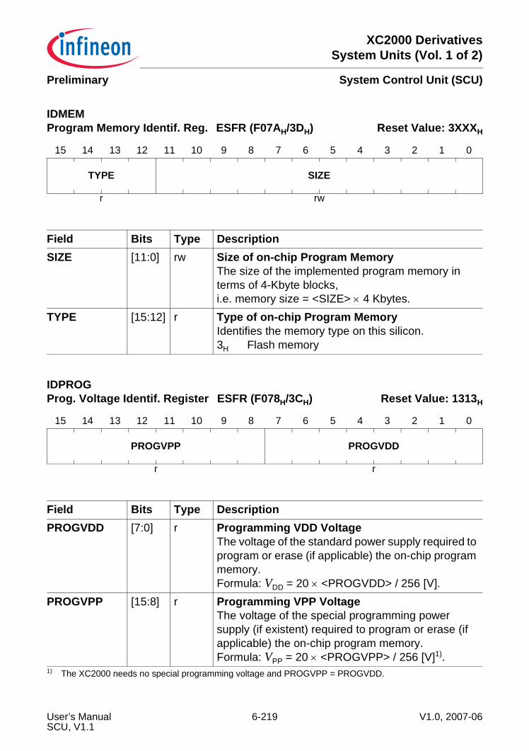
XC2000 DerivativesSystem Units (Vol. 1 of 2)
System Control Unit (SCU)Preliminary
IDMEMProgram Memory Identif. Reg. ESFR (F07AH/3DH) Reset Value: 3XXXH
15 14 13 12 11 10 9 8 7 6 5 4 3 2 1 0
TYPE SIZE
r rw
Field Bits Type DescriptionSIZE [11:0] rw Size of on-chip Program Memory
The size of the implemented program memory in terms of 4-Kbyte blocks,i.e. memory size = <SIZE> × 4 Kbytes.
TYPE [15:12] r Type of on-chip Program MemoryIdentifies the memory type on this silicon.3H Flash memory
IDPROGProg. Voltage Identif. Register ESFR (F078H/3CH) Reset Value: 1313H
15 14 13 12 11 10 9 8 7 6 5 4 3 2 1 0
PROGVPP PROGVDD
r r
Field Bits Type DescriptionPROGVDD [7:0] r Programming VDD Voltage
The voltage of the standard power supply required to program or erase (if applicable) the on-chip program memory.Formula: VDD = 20 × <PROGVDD> / 256 [V].
PROGVPP [15:8] r Programming VPP VoltageThe voltage of the special programming power supply (if existent) required to program or erase (if applicable) the on-chip program memory.Formula: VPP = 20 × <PROGVPP> / 256 [V]1).
1) The XC2000 needs no special programming voltage and PROGVPP = PROGVDD.
User’s Manual 6-219 V1.0, 2007-06SCU, V1.1
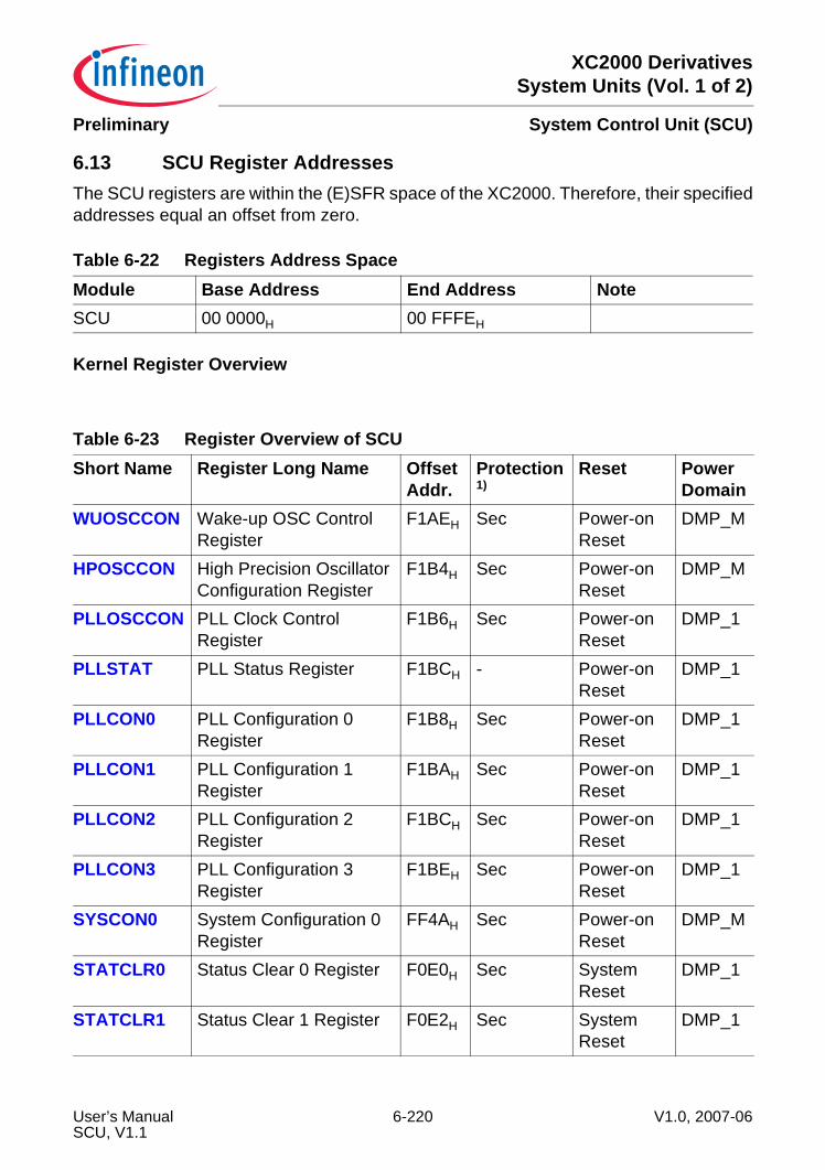
XC2000 DerivativesSystem Units (Vol. 1 of 2)
System Control Unit (SCU)Preliminary
6.13 SCU Register AddressesThe SCU registers are within the (E)SFR space of the XC2000. Therefore, their specifiedaddresses equal an offset from zero.
Kernel Register Overview
Table 6-22 Registers Address SpaceModule Base Address End Address NoteSCU 00 0000H 00 FFFEH
Table 6-23 Register Overview of SCUShort Name Register Long Name Offset
Addr.Protection1)
Reset Power Domain
WUOSCCON Wake-up OSC Control Register
F1AEH Sec Power-on Reset
DMP_M
HPOSCCON High Precision Oscillator Configuration Register
F1B4H Sec Power-on Reset
DMP_M
PLLOSCCON PLL Clock Control Register
F1B6H Sec Power-on Reset
DMP_1
PLLSTAT PLL Status Register F1BCH - Power-on Reset
DMP_1
PLLCON0 PLL Configuration 0 Register
F1B8H Sec Power-on Reset
DMP_1
PLLCON1 PLL Configuration 1 Register
F1BAH Sec Power-on Reset
DMP_1
PLLCON2 PLL Configuration 2 Register
F1BCH Sec Power-on Reset
DMP_1
PLLCON3 PLL Configuration 3 Register
F1BEH Sec Power-on Reset
DMP_1
SYSCON0 System Configuration 0 Register
FF4AH Sec Power-on Reset
DMP_M
STATCLR0 Status Clear 0 Register F0E0H Sec System Reset
DMP_1
STATCLR1 Status Clear 1 Register F0E2H Sec System Reset
DMP_1
User’s Manual 6-220 V1.0, 2007-06SCU, V1.1
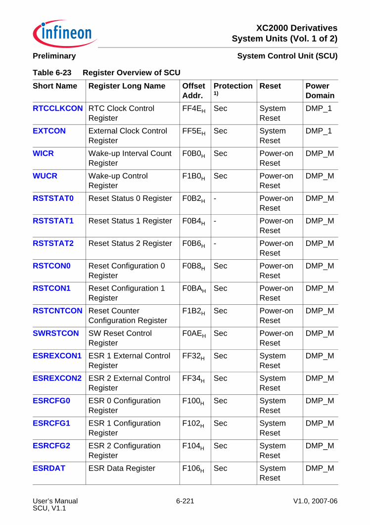
XC2000 DerivativesSystem Units (Vol. 1 of 2)
System Control Unit (SCU)Preliminary
RTCCLKCON RTC Clock Control Register
FF4EH Sec System Reset
DMP_1
EXTCON External Clock Control Register
FF5EH Sec System Reset
DMP_1
WICR Wake-up Interval Count Register
F0B0H Sec Power-on Reset
DMP_M
WUCR Wake-up Control Register
F1B0H Sec Power-on Reset
DMP_M
RSTSTAT0 Reset Status 0 Register F0B2H - Power-on Reset
DMP_M
RSTSTAT1 Reset Status 1 Register F0B4H - Power-on Reset
DMP_M
RSTSTAT2 Reset Status 2 Register F0B6H - Power-on Reset
DMP_M
RSTCON0 Reset Configuration 0 Register
F0B8H Sec Power-on Reset
DMP_M
RSTCON1 Reset Configuration 1 Register
F0BAH Sec Power-on Reset
DMP_M
RSTCNTCON Reset Counter Configuration Register
F1B2H Sec Power-on Reset
DMP_M
SWRSTCON SW Reset Control Register
F0AEH Sec Power-on Reset
DMP_M
ESREXCON1 ESR 1 External Control Register
FF32H Sec System Reset
DMP_M
ESREXCON2 ESR 2 External Control Register
FF34H Sec System Reset
DMP_M
ESRCFG0 ESR 0 Configuration Register
F100H Sec System Reset
DMP_M
ESRCFG1 ESR 1 Configuration Register
F102H Sec System Reset
DMP_M
ESRCFG2 ESR 2 Configuration Register
F104H Sec System Reset
DMP_M
ESRDAT ESR Data Register F106H Sec System Reset
DMP_M
Table 6-23 Register Overview of SCUShort Name Register Long Name Offset
Addr.Protection1)
Reset Power Domain
User’s Manual 6-221 V1.0, 2007-06SCU, V1.1
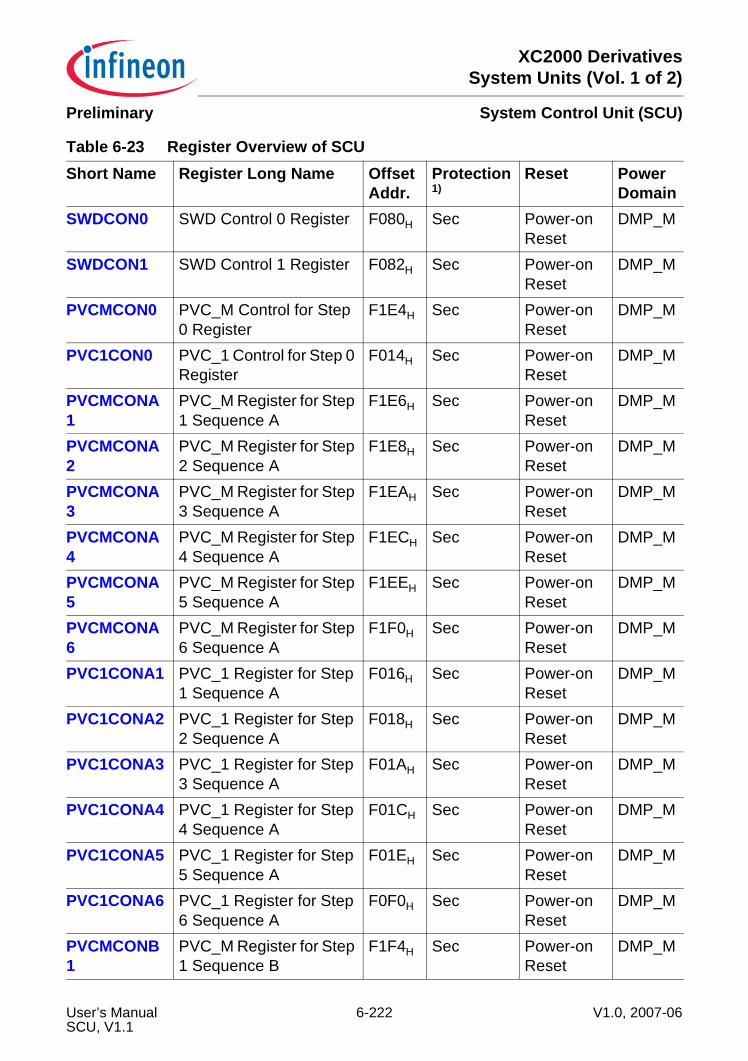
XC2000 DerivativesSystem Units (Vol. 1 of 2)
System Control Unit (SCU)Preliminary
SWDCON0 SWD Control 0 Register F080H Sec Power-on Reset
DMP_M
SWDCON1 SWD Control 1 Register F082H Sec Power-on Reset
DMP_M
PVCMCON0 PVC_M Control for Step 0 Register
F1E4H Sec Power-on Reset
DMP_M
PVC1CON0 PVC_1 Control for Step 0 Register
F014H Sec Power-on Reset
DMP_M
PVCMCONA1
PVC_M Register for Step 1 Sequence A
F1E6H Sec Power-on Reset
DMP_M
PVCMCONA2
PVC_M Register for Step 2 Sequence A
F1E8H Sec Power-on Reset
DMP_M
PVCMCONA3
PVC_M Register for Step 3 Sequence A
F1EAH Sec Power-on Reset
DMP_M
PVCMCONA4
PVC_M Register for Step 4 Sequence A
F1ECH Sec Power-on Reset
DMP_M
PVCMCONA5
PVC_M Register for Step 5 Sequence A
F1EEH Sec Power-on Reset
DMP_M
PVCMCONA6
PVC_M Register for Step 6 Sequence A
F1F0H Sec Power-on Reset
DMP_M
PVC1CONA1 PVC_1 Register for Step 1 Sequence A
F016H Sec Power-on Reset
DMP_M
PVC1CONA2 PVC_1 Register for Step 2 Sequence A
F018H Sec Power-on Reset
DMP_M
PVC1CONA3 PVC_1 Register for Step 3 Sequence A
F01AH Sec Power-on Reset
DMP_M
PVC1CONA4 PVC_1 Register for Step 4 Sequence A
F01CH Sec Power-on Reset
DMP_M
PVC1CONA5 PVC_1 Register for Step 5 Sequence A
F01EH Sec Power-on Reset
DMP_M
PVC1CONA6 PVC_1 Register for Step 6 Sequence A
F0F0H Sec Power-on Reset
DMP_M
PVCMCONB1
PVC_M Register for Step 1 Sequence B
F1F4H Sec Power-on Reset
DMP_M
Table 6-23 Register Overview of SCUShort Name Register Long Name Offset
Addr.Protection1)
Reset Power Domain
User’s Manual 6-222 V1.0, 2007-06SCU, V1.1
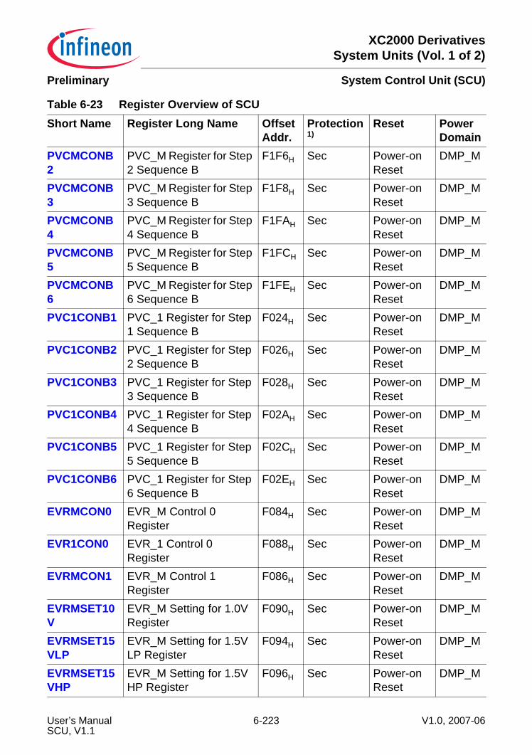
XC2000 DerivativesSystem Units (Vol. 1 of 2)
System Control Unit (SCU)Preliminary
PVCMCONB2
PVC_M Register for Step 2 Sequence B
F1F6H Sec Power-on Reset
DMP_M
PVCMCONB3
PVC_M Register for Step 3 Sequence B
F1F8H Sec Power-on Reset
DMP_M
PVCMCONB4
PVC_M Register for Step 4 Sequence B
F1FAH Sec Power-on Reset
DMP_M
PVCMCONB5
PVC_M Register for Step 5 Sequence B
F1FCH Sec Power-on Reset
DMP_M
PVCMCONB6
PVC_M Register for Step 6 Sequence B
F1FEH Sec Power-on Reset
DMP_M
PVC1CONB1 PVC_1 Register for Step 1 Sequence B
F024H Sec Power-on Reset
DMP_M
PVC1CONB2 PVC_1 Register for Step 2 Sequence B
F026H Sec Power-on Reset
DMP_M
PVC1CONB3 PVC_1 Register for Step 3 Sequence B
F028H Sec Power-on Reset
DMP_M
PVC1CONB4 PVC_1 Register for Step 4 Sequence B
F02AH Sec Power-on Reset
DMP_M
PVC1CONB5 PVC_1 Register for Step 5 Sequence B
F02CH Sec Power-on Reset
DMP_M
PVC1CONB6 PVC_1 Register for Step 6 Sequence B
F02EH Sec Power-on Reset
DMP_M
EVRMCON0 EVR_M Control 0 Register
F084H Sec Power-on Reset
DMP_M
EVR1CON0 EVR_1 Control 0 Register
F088H Sec Power-on Reset
DMP_M
EVRMCON1 EVR_M Control 1 Register
F086H Sec Power-on Reset
DMP_M
EVRMSET10V
EVR_M Setting for 1.0V Register
F090H Sec Power-on Reset
DMP_M
EVRMSET15VLP
EVR_M Setting for 1.5V LP Register
F094H Sec Power-on Reset
DMP_M
EVRMSET15VHP
EVR_M Setting for 1.5V HP Register
F096H Sec Power-on Reset
DMP_M
Table 6-23 Register Overview of SCUShort Name Register Long Name Offset
Addr.Protection1)
Reset Power Domain
User’s Manual 6-223 V1.0, 2007-06SCU, V1.1
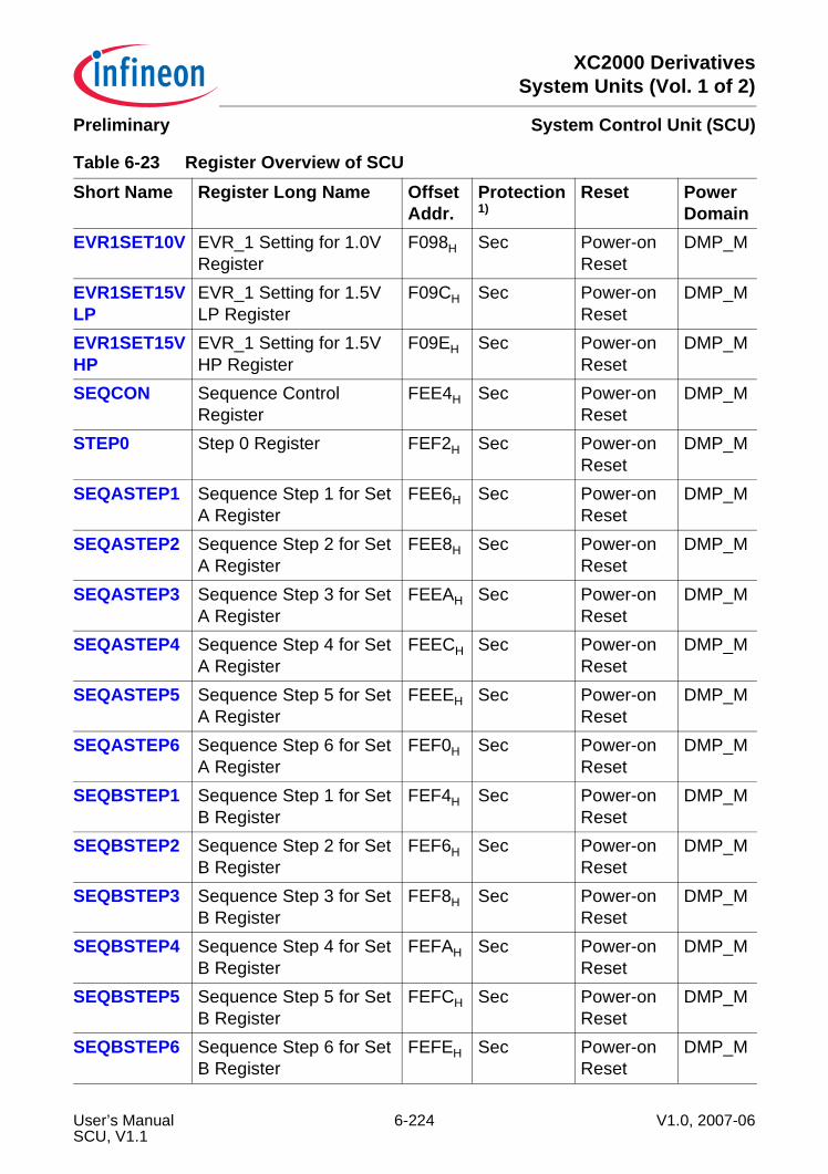
XC2000 DerivativesSystem Units (Vol. 1 of 2)
System Control Unit (SCU)Preliminary
EVR1SET10V EVR_1 Setting for 1.0V Register
F098H Sec Power-on Reset
DMP_M
EVR1SET15VLP
EVR_1 Setting for 1.5V LP Register
F09CH Sec Power-on Reset
DMP_M
EVR1SET15VHP
EVR_1 Setting for 1.5V HP Register
F09EH Sec Power-on Reset
DMP_M
SEQCON Sequence Control Register
FEE4H Sec Power-on Reset
DMP_M
STEP0 Step 0 Register FEF2H Sec Power-on Reset
DMP_M
SEQASTEP1 Sequence Step 1 for Set A Register
FEE6H Sec Power-on Reset
DMP_M
SEQASTEP2 Sequence Step 2 for Set A Register
FEE8H Sec Power-on Reset
DMP_M
SEQASTEP3 Sequence Step 3 for Set A Register
FEEAH Sec Power-on Reset
DMP_M
SEQASTEP4 Sequence Step 4 for Set A Register
FEECH Sec Power-on Reset
DMP_M
SEQASTEP5 Sequence Step 5 for Set A Register
FEEEH Sec Power-on Reset
DMP_M
SEQASTEP6 Sequence Step 6 for Set A Register
FEF0H Sec Power-on Reset
DMP_M
SEQBSTEP1 Sequence Step 1 for Set B Register
FEF4H Sec Power-on Reset
DMP_M
SEQBSTEP2 Sequence Step 2 for Set B Register
FEF6H Sec Power-on Reset
DMP_M
SEQBSTEP3 Sequence Step 3 for Set B Register
FEF8H Sec Power-on Reset
DMP_M
SEQBSTEP4 Sequence Step 4 for Set B Register
FEFAH Sec Power-on Reset
DMP_M
SEQBSTEP5 Sequence Step 5 for Set B Register
FEFCH Sec Power-on Reset
DMP_M
SEQBSTEP6 Sequence Step 6 for Set B Register
FEFEH Sec Power-on Reset
DMP_M
Table 6-23 Register Overview of SCUShort Name Register Long Name Offset
Addr.Protection1)
Reset Power Domain
User’s Manual 6-224 V1.0, 2007-06SCU, V1.1
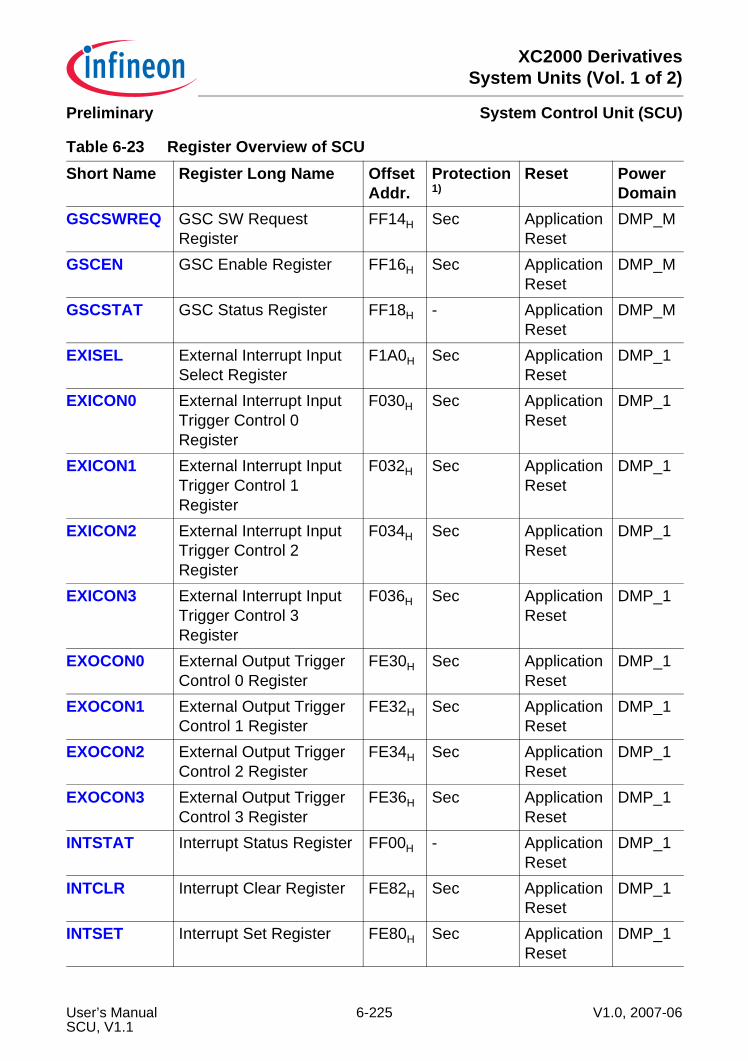
XC2000 DerivativesSystem Units (Vol. 1 of 2)
System Control Unit (SCU)Preliminary
GSCSWREQ GSC SW Request Register
FF14H Sec Application Reset
DMP_M
GSCEN GSC Enable Register FF16H Sec Application Reset
DMP_M
GSCSTAT GSC Status Register FF18H - Application Reset
DMP_M
EXISEL External Interrupt Input Select Register
F1A0H Sec Application Reset
DMP_1
EXICON0 External Interrupt Input Trigger Control 0 Register
F030H Sec Application Reset
DMP_1
EXICON1 External Interrupt Input Trigger Control 1 Register
F032H Sec Application Reset
DMP_1
EXICON2 External Interrupt Input Trigger Control 2 Register
F034H Sec Application Reset
DMP_1
EXICON3 External Interrupt Input Trigger Control 3 Register
F036H Sec Application Reset
DMP_1
EXOCON0 External Output Trigger Control 0 Register
FE30H Sec Application Reset
DMP_1
EXOCON1 External Output Trigger Control 1 Register
FE32H Sec Application Reset
DMP_1
EXOCON2 External Output Trigger Control 2 Register
FE34H Sec Application Reset
DMP_1
EXOCON3 External Output Trigger Control 3 Register
FE36H Sec Application Reset
DMP_1
INTSTAT Interrupt Status Register FF00H - Application Reset
DMP_1
INTCLR Interrupt Clear Register FE82H Sec Application Reset
DMP_1
INTSET Interrupt Set Register FE80H Sec Application Reset
DMP_1
Table 6-23 Register Overview of SCUShort Name Register Long Name Offset
Addr.Protection1)
Reset Power Domain
User’s Manual 6-225 V1.0, 2007-06SCU, V1.1
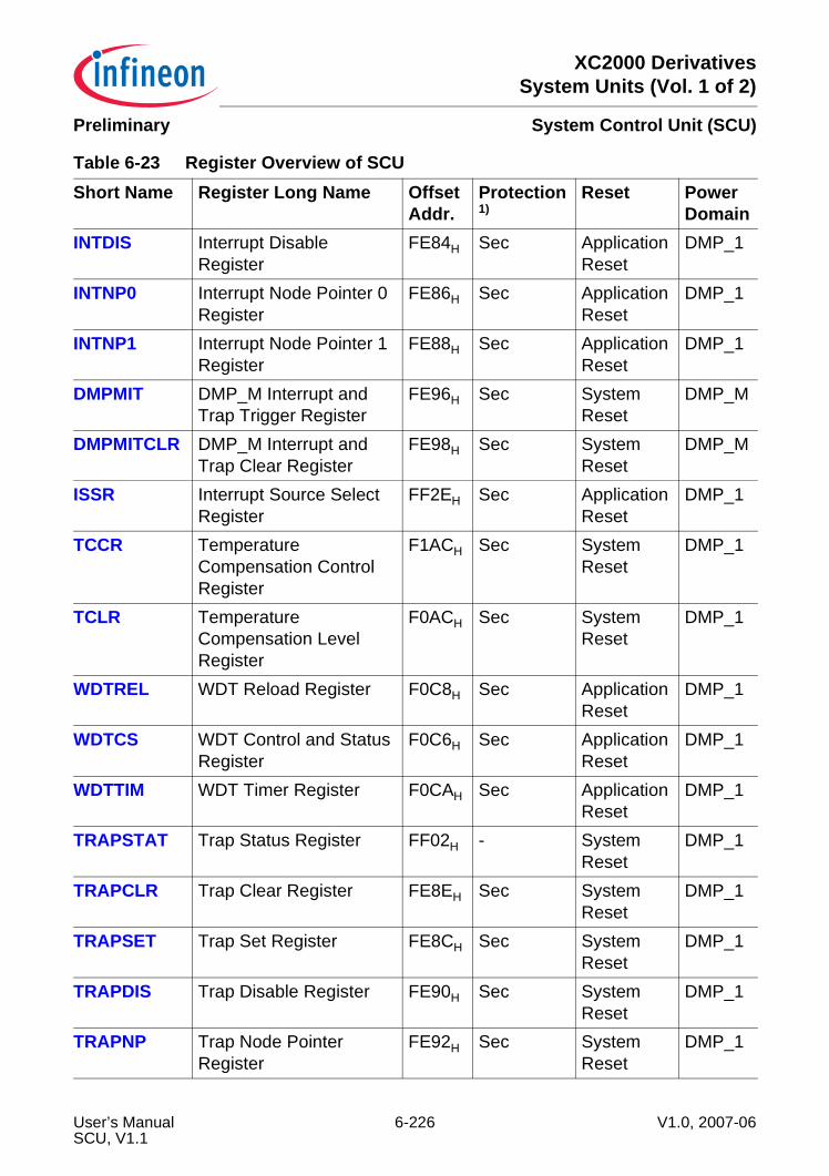
XC2000 DerivativesSystem Units (Vol. 1 of 2)
System Control Unit (SCU)Preliminary
INTDIS Interrupt Disable Register
FE84H Sec Application Reset
DMP_1
INTNP0 Interrupt Node Pointer 0 Register
FE86H Sec Application Reset
DMP_1
INTNP1 Interrupt Node Pointer 1 Register
FE88H Sec Application Reset
DMP_1
DMPMIT DMP_M Interrupt and Trap Trigger Register
FE96H Sec System Reset
DMP_M
DMPMITCLR DMP_M Interrupt and Trap Clear Register
FE98H Sec System Reset
DMP_M
ISSR Interrupt Source Select Register
FF2EH Sec Application Reset
DMP_1
TCCR Temperature Compensation Control Register
F1ACH Sec System Reset
DMP_1
TCLR Temperature Compensation Level Register
F0ACH Sec System Reset
DMP_1
WDTREL WDT Reload Register F0C8H Sec Application Reset
DMP_1
WDTCS WDT Control and Status Register
F0C6H Sec Application Reset
DMP_1
WDTTIM WDT Timer Register F0CAH Sec Application Reset
DMP_1
TRAPSTAT Trap Status Register FF02H - System Reset
DMP_1
TRAPCLR Trap Clear Register FE8EH Sec System Reset
DMP_1
TRAPSET Trap Set Register FE8CH Sec System Reset
DMP_1
TRAPDIS Trap Disable Register FE90H Sec System Reset
DMP_1
TRAPNP Trap Node Pointer Register
FE92H Sec System Reset
DMP_1
Table 6-23 Register Overview of SCUShort Name Register Long Name Offset
Addr.Protection1)
Reset Power Domain
User’s Manual 6-226 V1.0, 2007-06SCU, V1.1
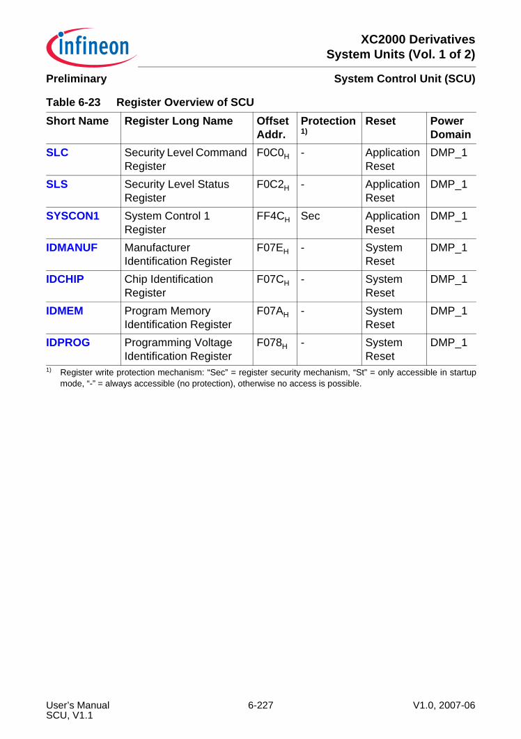
XC2000 DerivativesSystem Units (Vol. 1 of 2)
System Control Unit (SCU)Preliminary
SLC Security Level Command Register
F0C0H - Application Reset
DMP_1
SLS Security Level Status Register
F0C2H - Application Reset
DMP_1
SYSCON1 System Control 1 Register
FF4CH Sec Application Reset
DMP_1
IDMANUF Manufacturer Identification Register
F07EH - System Reset
DMP_1
IDCHIP Chip Identification Register
F07CH - System Reset
DMP_1
IDMEM Program Memory Identification Register
F07AH - System Reset
DMP_1
IDPROG Programming Voltage Identification Register
F078H - System Reset
DMP_1
1) Register write protection mechanism: “Sec” = register security mechanism, “St” = only accessible in startupmode, “-” = always accessible (no protection), otherwise no access is possible.
Table 6-23 Register Overview of SCUShort Name Register Long Name Offset
Addr.Protection1)
Reset Power Domain
User’s Manual 6-227 V1.0, 2007-06SCU, V1.1
XC2000 DerivativesSystem Units (Vol. 1 of 2)
System Control Unit (SCU)Preliminary
User’s Manual 6-228 V1.0, 2007-06SCU, V1.1
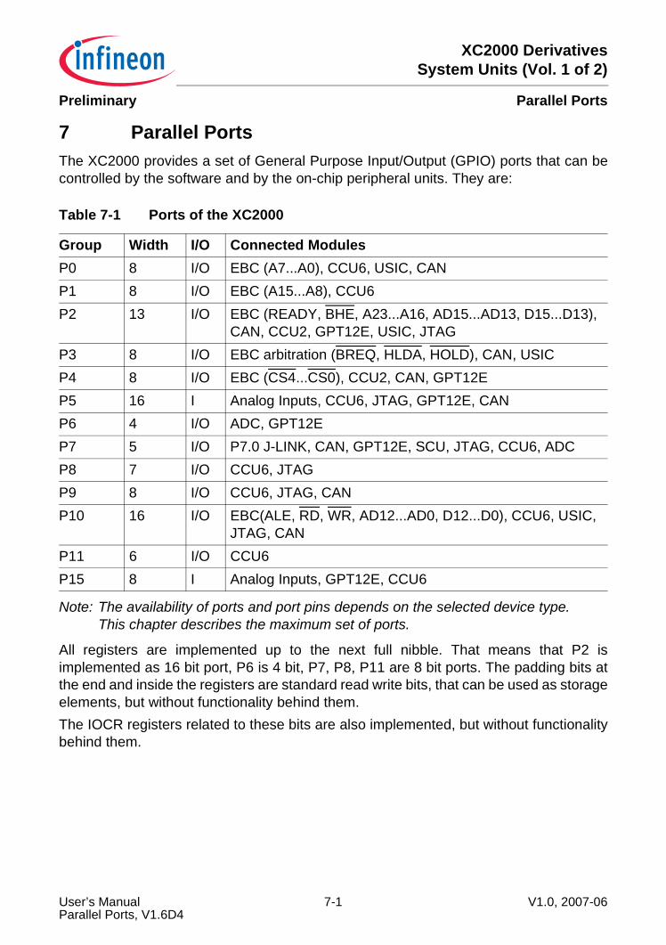
XC2000 DerivativesSystem Units (Vol. 1 of 2)
Parallel PortsPreliminary
7 Parallel PortsThe XC2000 provides a set of General Purpose Input/Output (GPIO) ports that can becontrolled by the software and by the on-chip peripheral units. They are:
Note: The availability of ports and port pins depends on the selected device type.This chapter describes the maximum set of ports.
All registers are implemented up to the next full nibble. That means that P2 isimplemented as 16 bit port, P6 is 4 bit, P7, P8, P11 are 8 bit ports. The padding bits atthe end and inside the registers are standard read write bits, that can be used as storageelements, but without functionality behind them.The IOCR registers related to these bits are also implemented, but without functionalitybehind them.
Table 7-1 Ports of the XC2000
Group Width I/O Connected ModulesP0 8 I/O EBC (A7...A0), CCU6, USIC, CANP1 8 I/O EBC (A15...A8), CCU6P2 13 I/O EBC (READY, BHE, A23...A16, AD15...AD13, D15...D13),
CAN, CCU2, GPT12E, USIC, JTAGP3 8 I/O EBC arbitration (BREQ, HLDA, HOLD), CAN, USICP4 8 I/O EBC (CS4...CS0), CCU2, CAN, GPT12EP5 16 I Analog Inputs, CCU6, JTAG, GPT12E, CANP6 4 I/O ADC, GPT12EP7 5 I/O P7.0 J-LINK, CAN, GPT12E, SCU, JTAG, CCU6, ADCP8 7 I/O CCU6, JTAGP9 8 I/O CCU6, JTAG, CANP10 16 I/O EBC(ALE, RD, WR, AD12...AD0, D12...D0), CCU6, USIC,
JTAG, CANP11 6 I/O CCU6P15 8 I Analog Inputs, GPT12E, CCU6
User’s Manual 7-1 V1.0, 2007-06Parallel Ports, V1.6D4
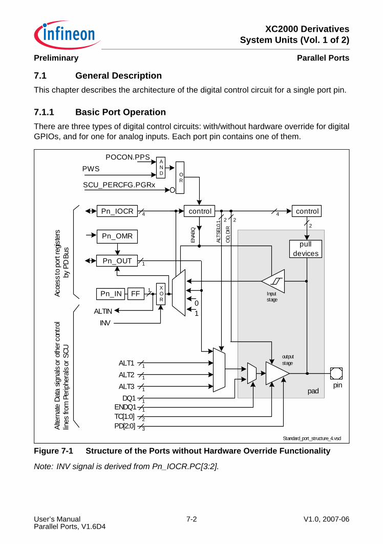
XC2000 DerivativesSystem Units (Vol. 1 of 2)
Parallel PortsPreliminary
7.1 General DescriptionThis chapter describes the architecture of the digital control circuit for a single port pin.
7.1.1 Basic Port OperationThere are three types of digital control circuits: with/without hardware override for digitalGPIOs, and for one for analog inputs. Each port pin contains one of them.
Figure 7-1 Structure of the Ports without Hardware Override Functionality
Note: INV signal is derived from Pn_IOCR.PC[3:2].
pin
ALT1
Pn_IOCR
ALT2ALT3
TC[1:0]PD[2:0]
1
1
1
pulldevices
4 control
22
Standard_port_structure_4.vsd
Acce
ss to
por
t reg
iste
rs b
y PD
Bus
Alte
rnat
e Da
ta s
igna
ls or
oth
er c
ontro
llin
es fr
om P
erip
hera
ls or
SCU
outputstage
pad
4
OD,
DIR
DQ1ENDQ1 1
3
1
2
Pn_IN
ALTIN
Inputstage
Pn_OUT 1
Pn_OMR
XOR
INV
2AL
TSEL
0,1
control
POCON.PPS
01
AND O
RSCU_PERCFG.PGRx
PWS
ENAB
Q
FF 1
User’s Manual 7-2 V1.0, 2007-06Parallel Ports, V1.6D4
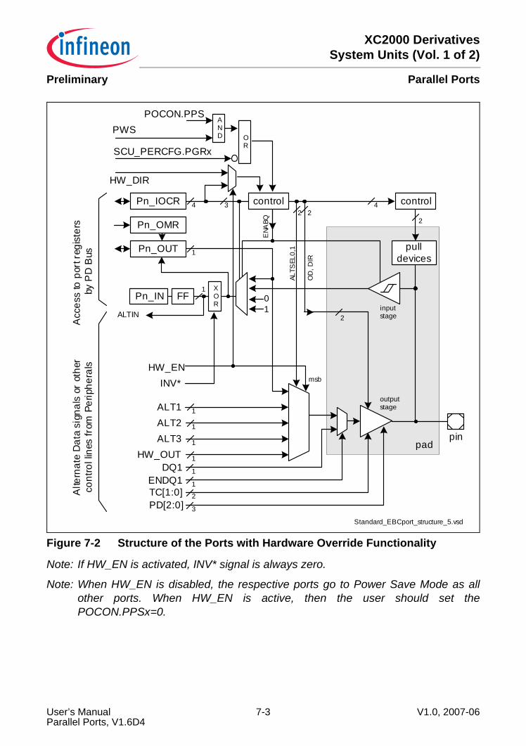
XC2000 DerivativesSystem Units (Vol. 1 of 2)
Parallel PortsPreliminary
Figure 7-2 Structure of the Ports with Hardware Override Functionality
Note: If HW_EN is activated, INV* signal is always zero.
Note: When HW_EN is disabled, the respective ports go to Power Save Mode as allother ports. When HW_EN is active, then the user should set thePOCON.PPSx=0.
ENA
BQ
pin
ALT1
Pn_OUT
Pn_IN
Pn_OMR
Pn_IOCR
ALT21
1
1
1
pulldevices
24 control
22
Acc
ess
to p
ort r
egis
ters
by
PD
Bus
Alte
rnat
e D
ata
sign
als
or o
ther
cont
rol l
ines
from
Per
iphe
rals
inputstage
outputstage
ALTIN
pad
4
ALTS
EL0,
1
TC[1:0]PD[2:0]
DQ1ENDQ1 1
3
1
2
ALT3 1
HW_OUT 1
HW_DIR
2O
D, D
IR
msb
Standard_EBCport_structure_5.vsd
XOR
INV*
01
POCON.PPSAND O
RSCU_PERCFG.PGRx
PWS
control3
HW_EN
FF
User’s Manual 7-3 V1.0, 2007-06Parallel Ports, V1.6D4
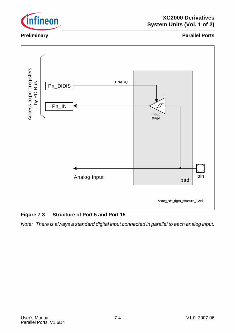
XC2000 DerivativesSystem Units (Vol. 1 of 2)
Parallel PortsPreliminary
Figure 7-3 Structure of Port 5 and Port 15
Note: There is always a standard digital input connected in parallel to each analog input.
pin
Analog_port_digital_structure_2.vsd
Acc
ess
to p
ort r
egis
ters
by
PD
Bus
pad
Pn_INInputstage
Pn_DIDIS
Analog Input
ENABQ
User’s Manual 7-4 V1.0, 2007-06Parallel Ports, V1.6D4
XC2000 DerivativesSystem Units (Vol. 1 of 2)
Parallel PortsPreliminary
7.1.2 Input Stage ControlAn input stage consists of a Schmitt trigger, which can be enabled or disabled viasoftware, and an input multiplexer that by default selects the output of the inputSchmitt trigger.A disabled input driver drives high logical level. During and after reset, all input stagesare enabled by default.
7.1.3 Output Driver ControlAn output stage consists of an output driver, output multiplexer, and register bit fields fortheir control.
7.1.3.1 Active Mode BehaviorEach output driver can be configured in a push-pull or an open-drain mode, or it can bedeactivated (three-stated). An output multiplexer in front of the output driver selects thesignal source, choosing either the appropriate bit of the Pn_OUT register, or one ofmaximum three lines coming from a peripheral unit, see Figure 7-1. The selection isdone via the Pn_IOCR register. Software can set or clear the bit Pn_OUT.Px, whichdrives the port pin in case it is selected by the output multiplexer.An output driver with hardware override can select an additional output signal comingfrom a peripheral. While the hardware override is activated, this signal has higher prioritythan all other output signals and can not be deselected by the port. In this case, theperipheral controls the direction of the pin.
7.1.3.2 Power Saving Mode BehaviorIn Power Saving Mode (core and IO supply voltages available), the behavior of a pindepends on the setting of the POCONx.PPSx bit. Basically, groups of four pins within aport can be configured to react to Power Save Mode Request or to ignore it. In case apin group is configured to react to a Power Save Mode Request, each pin within a groupreacts according to its own configuration according to the Table 7-5.
7.1.3.3 Reset BehaviorDuring reset, all output stages of GPIO pins go to tri-state mode without any pull-up orpull-down device.
7.1.3.4 Power-fail BehaviorWhen the core supply fails while the pad supply remains stable, the output stages go intotri-state mode.
User’s Manual 7-5 V1.0, 2007-06Parallel Ports, V1.6D4
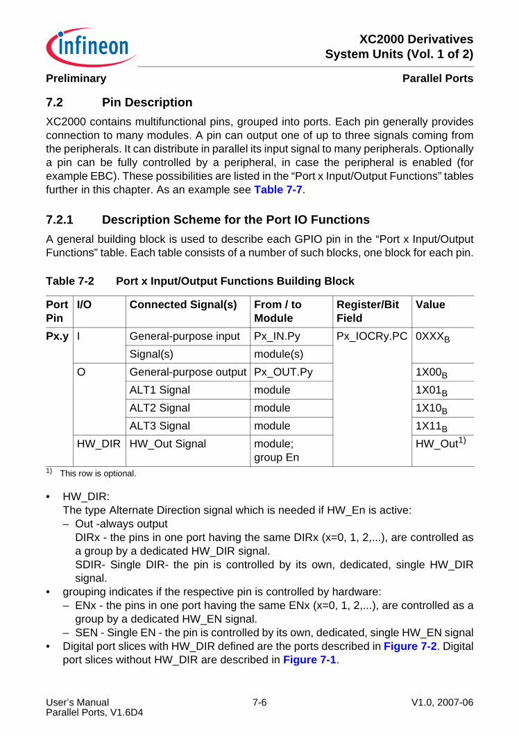
XC2000 DerivativesSystem Units (Vol. 1 of 2)
Parallel PortsPreliminary
7.2 Pin DescriptionXC2000 contains multifunctional pins, grouped into ports. Each pin generally providesconnection to many modules. A pin can output one of up to three signals coming fromthe peripherals. It can distribute in parallel its input signal to many peripherals. Optionallya pin can be fully controlled by a peripheral, in case the peripheral is enabled (forexample EBC). These possibilities are listed in the “Port x Input/Output Functions” tablesfurther in this chapter. As an example see Table 7-7.
7.2.1 Description Scheme for the Port IO FunctionsA general building block is used to describe each GPIO pin in the “Port x Input/OutputFunctions” table. Each table consists of a number of such blocks, one block for each pin.
• HW_DIR: The type Alternate Direction signal which is needed if HW_En is active:– Out -always output
DIRx - the pins in one port having the same DIRx (x=0, 1, 2,...), are controlled asa group by a dedicated HW_DIR signal.SDIR- Single DIR- the pin is controlled by its own, dedicated, single HW_DIRsignal.
• grouping indicates if the respective pin is controlled by hardware:– ENx - the pins in one port having the same ENx (x=0, 1, 2,...), are controlled as a
group by a dedicated HW_EN signal.– SEN - Single EN - the pin is controlled by its own, dedicated, single HW_EN signal
• Digital port slices with HW_DIR defined are the ports described in Figure 7-2. Digitalport slices without HW_DIR are described in Figure 7-1.
Table 7-2 Port x Input/Output Functions Building Block
PortPin
I/O Connected Signal(s) From / to Module
Register/Bit Field
Value
Px.y I General-purpose input Px_IN.Py Px_IOCRy.PC 0XXXB
Signal(s) module(s)O General-purpose output Px_OUT.Py 1X00B
ALT1 Signal module 1X01B
ALT2 Signal module 1X10B
ALT3 Signal module 1X11B
HW_DIR HW_Out Signal module; group En
HW_Out1)
1) This row is optional.
User’s Manual 7-6 V1.0, 2007-06Parallel Ports, V1.6D4
XC2000 DerivativesSystem Units (Vol. 1 of 2)
Parallel PortsPreliminary
7.3 Port DescriptionThe bit positions in the port registers always start right-aligned. For example, a portcomprising only 8 pins only uses the bit positions [7:0] of the corresponding register. Theremaining bit positions are filled with 0 (r).The pad driver mode registers may be different for each port. As a result, they aredescribed independently for each port in the corresponding chapter.
7.3.1 Port Register Description
7.3.1.1 Pad Driver ControlThe pad structure used in this device offers the possibility to select the output driverstrength and the slew rate. These selections are independent from the output portfunctionality, such as open-drain, push/pull or input only.In order to minimize EMI problems, the driver strength can be adapted to the applicationrequirements by bit fields PDMx. The selection is done in groups of four pins.The Port Output Control registers POCON provide the corresponding control bits. A4-bit control field configures the driver strength and the edge shape. Word portsconsume four control nibbles each, byte ports consume two control nibbles each, whereeach control nibble controls 4 pins of the respective port.Note: P2_POCON register in the P11_MR contains an exception regarding the
additional strong output driver connected in parallel to the standard output driverof the P2.8 pin. See port 2 section.
User’s Manual 7-7 V1.0, 2007-06Parallel Ports, V1.6D4
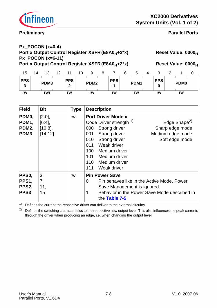
XC2000 DerivativesSystem Units (Vol. 1 of 2)
Parallel PortsPreliminary
Px_POCON (x=0-4) Port x Output Control Register XSFR (E8A0H+2*x) Reset Value: 0000HPx_POCON (x=6-11)Port x Output Control Register XSFR (E8A0H+2*x) Reset Value: 0000H
15 14 13 12 11 10 9 8 7 6 5 4 3 2 1 0
PPS3 PDM3 PPS
2 PDM2 PPS1 PDM1 PPS
0 PDM0
rw rwr rw rw rw rw rw rw
Field Bit Type DescriptionPDM0,PDM1,PDM2,PDM3
[2:0],[6:4],[10:8],[14:12]
rw Port Driver Mode xCode Driver strength 1) Edge Shape2)
000 Strong driver Sharp edge mode001 Strong driver Medium edge mode010 Strong driver Soft edge mode011 Weak driver 100 Medium driver101 Medium driver110 Medium driver111 Weak driver
1) Defines the current the respective driver can deliver to the external circuitry.2) Defines the switching characteristics to the respective new output level. This also influences the peak currents
through the driver when producing an edge, i.e. when changing the output level.
PPS0,PPS1,PPS2,PPS3
3,7,11,15
rw Pin Power Save0 Pin behaves like in the Active Mode. Power
Save Management is ignored.1 Behavior in the Power Save Mode described in
the Table 7-5.
User’s Manual 7-8 V1.0, 2007-06Parallel Ports, V1.6D4
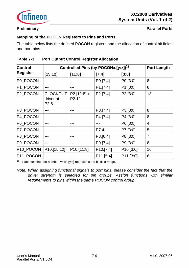
XC2000 DerivativesSystem Units (Vol. 1 of 2)
Parallel PortsPreliminary
Mapping of the POCON Registers to Pins and PortsThe table below lists the defined POCON registers and the allocation of control bit fieldsand port pins.
Note: When assigning functional signals to port pins, please consider the fact that thedriver strength is selected for pin groups. Assign functions with similarrequirements to pins within the same POCON control group.
Table 7-3 Port Output Control Register Allocation
Control Register
Controlled Pins (by POCONx.[y:z])1)
1) x denotes the port number, while [y:z] represents the bit field range.
Port Length[15:12] [11:8] [7:4] [3:0]
P0_POCON --- --- P0.[7:4] P0.[3:0] 8P1_POCON --- --- P1.[7:4] P1.[3:0] 8P2_POCON CLOCKOUT
driver at P2.8
P2.[11:8] + P2.12
P2.[7:4] P2.[3:0] 13
P3_POCON --- --- P3.[7:4] P3.[3:0] 8P4_POCON --- --- P4.[7:4] P4.[3:0] 8P6_POCON --- --- --- P6.[3:0] 4P7_POCON --- --- P7.4 P7.[3:0] 5P8_POCON --- --- P8.[6:4] P8.[3:0] 7P9_POCON --- --- P9.[7:4] P9.[3:0] 8P10_POCON P10.[15:12] P10.[11:8] P10.[7:4] P10.[3:0] 16P11_POCON --- --- P11.[5:4] P11.[3:0] 6
User’s Manual 7-9 V1.0, 2007-06Parallel Ports, V1.6D4
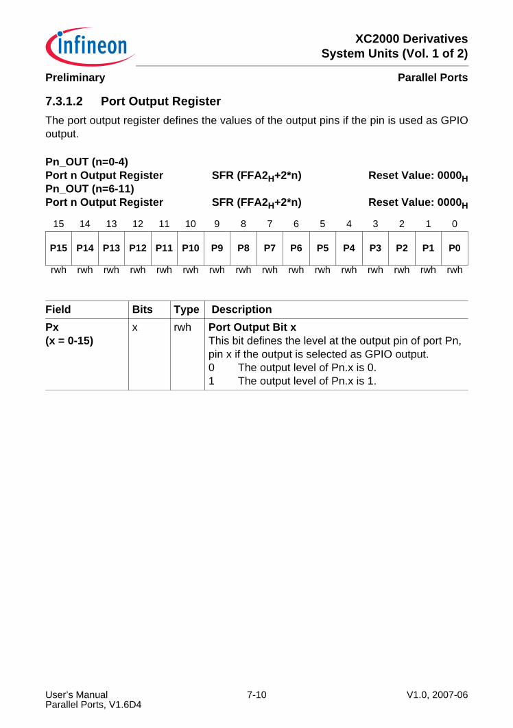
XC2000 DerivativesSystem Units (Vol. 1 of 2)
Parallel PortsPreliminary
7.3.1.2 Port Output RegisterThe port output register defines the values of the output pins if the pin is used as GPIOoutput.
Pn_OUT (n=0-4) Port n Output Register SFR (FFA2H+2*n) Reset Value: 0000HPn_OUT (n=6-11)Port n Output Register SFR (FFA2H+2*n) Reset Value: 0000H
15 14 13 12 11 10 9 8 7 6 5 4 3 2 1 0
P15 P14 P13 P12 P11 P10 P9 P8 P7 P6 P5 P4 P3 P2 P1 P0
rwh rwh rwh rwh rwh rwh rwh rwh rwh rwh rwh rwh rwh rwh rwh rwh
Field Bits Type DescriptionPx(x = 0-15)
x rwh Port Output Bit xThis bit defines the level at the output pin of port Pn, pin x if the output is selected as GPIO output.0 The output level of Pn.x is 0.1 The output level of Pn.x is 1.
User’s Manual 7-10 V1.0, 2007-06Parallel Ports, V1.6D4
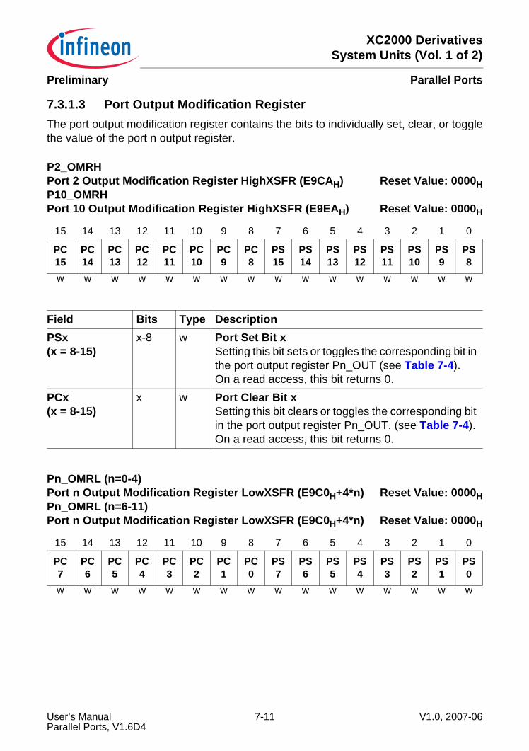
XC2000 DerivativesSystem Units (Vol. 1 of 2)
Parallel PortsPreliminary
7.3.1.3 Port Output Modification RegisterThe port output modification register contains the bits to individually set, clear, or togglethe value of the port n output register.
P2_OMRH Port 2 Output Modification Register HighXSFR (E9CAH) Reset Value: 0000HP10_OMRH Port 10 Output Modification Register HighXSFR (E9EAH) Reset Value: 0000H
15 14 13 12 11 10 9 8 7 6 5 4 3 2 1 0
PC15
PC14
PC13
PC12
PC11
PC10
PC9
PC8
PS15
PS14
PS13
PS12
PS11
PS10
PS9
PS8
w w w w w w w w w w w w w w w w
Field Bits Type DescriptionPSx(x = 8-15)
x-8 w Port Set Bit xSetting this bit sets or toggles the corresponding bit in the port output register Pn_OUT (see Table 7-4).On a read access, this bit returns 0.
PCx(x = 8-15)
x w Port Clear Bit xSetting this bit clears or toggles the corresponding bit in the port output register Pn_OUT. (see Table 7-4).On a read access, this bit returns 0.
Pn_OMRL (n=0-4) Port n Output Modification Register LowXSFR (E9C0H+4*n) Reset Value: 0000HPn_OMRL (n=6-11)Port n Output Modification Register LowXSFR (E9C0H+4*n) Reset Value: 0000H
15 14 13 12 11 10 9 8 7 6 5 4 3 2 1 0
PC7
PC6
PC5
PC4
PC3
PC2
PC1
PC0
PS7
PS6
PS5
PS4
PS3
PS2
PS1
PS0
w w w w w w w w w w w w w w w w
User’s Manual 7-11 V1.0, 2007-06Parallel Ports, V1.6D4
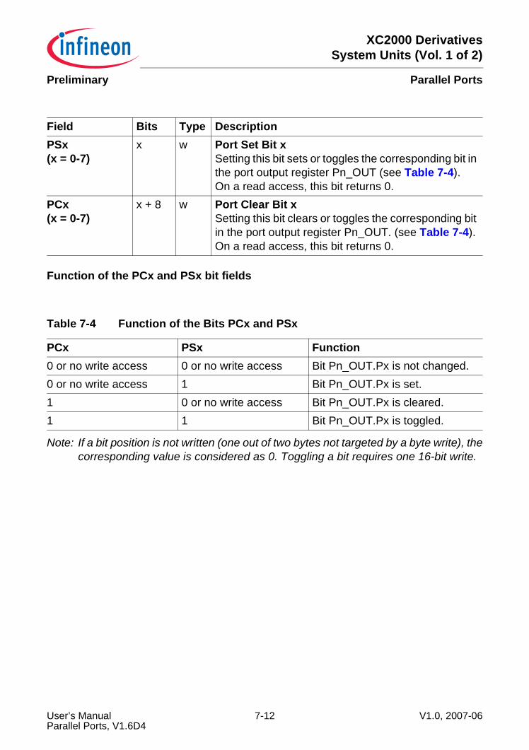
XC2000 DerivativesSystem Units (Vol. 1 of 2)
Parallel PortsPreliminary
Function of the PCx and PSx bit fields
Note: If a bit position is not written (one out of two bytes not targeted by a byte write), thecorresponding value is considered as 0. Toggling a bit requires one 16-bit write.
Field Bits Type DescriptionPSx(x = 0-7)
x w Port Set Bit xSetting this bit sets or toggles the corresponding bit in the port output register Pn_OUT (see Table 7-4).On a read access, this bit returns 0.
PCx(x = 0-7)
x + 8 w Port Clear Bit xSetting this bit clears or toggles the corresponding bit in the port output register Pn_OUT. (see Table 7-4).On a read access, this bit returns 0.
Table 7-4 Function of the Bits PCx and PSx
PCx PSx Function0 or no write access 0 or no write access Bit Pn_OUT.Px is not changed.0 or no write access 1 Bit Pn_OUT.Px is set.1 0 or no write access Bit Pn_OUT.Px is cleared.1 1 Bit Pn_OUT.Px is toggled.
User’s Manual 7-12 V1.0, 2007-06Parallel Ports, V1.6D4
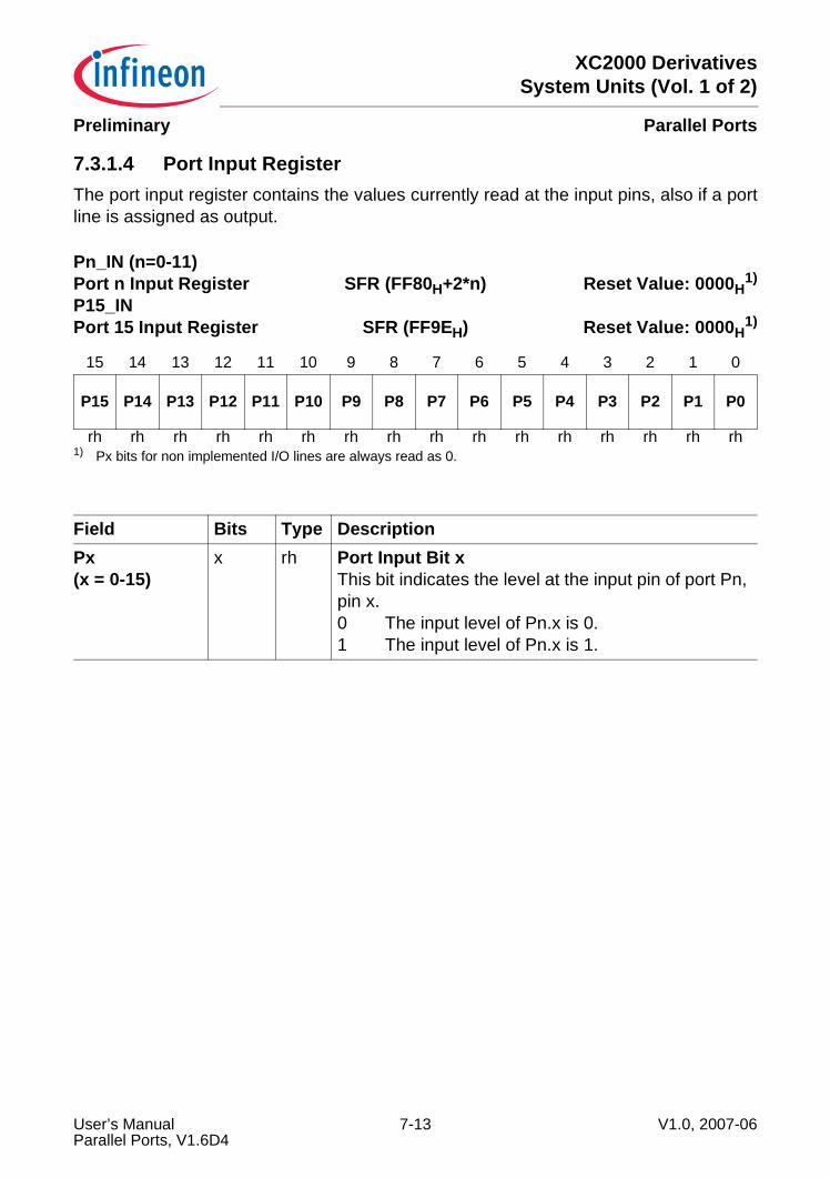
XC2000 DerivativesSystem Units (Vol. 1 of 2)
Parallel PortsPreliminary
7.3.1.4 Port Input RegisterThe port input register contains the values currently read at the input pins, also if a portline is assigned as output.
Pn_IN (n=0-11) Port n Input Register SFR (FF80H+2*n) Reset Value: 0000H
1)
P15_INPort 15 Input Register SFR (FF9EH) Reset Value: 0000H
1)
1) Px bits for non implemented I/O lines are always read as 0.
15 14 13 12 11 10 9 8 7 6 5 4 3 2 1 0
P15 P14 P13 P12 P11 P10 P9 P8 P7 P6 P5 P4 P3 P2 P1 P0
rh rh rh rh rh rh rh rh rh rh rh rh rh rh rh rh
Field Bits Type DescriptionPx(x = 0-15)
x rh Port Input Bit xThis bit indicates the level at the input pin of port Pn, pin x.0 The input level of Pn.x is 0.1 The input level of Pn.x is 1.
User’s Manual 7-13 V1.0, 2007-06Parallel Ports, V1.6D4

XC2000 DerivativesSystem Units (Vol. 1 of 2)
Parallel PortsPreliminary
7.3.1.5 Port Input/Output Control RegistersThe port input/output control registers contain the bit fields to select the digital output andinput driver characteristics, such as pull-up/down devices, port direction (input/output),open-drain and alternate output selections. The coding of the options is shown inTable 7-5.Depending on the port functionality not all of the input/output control registers may beimplemented. The structure with one control bit field for each port pin located in differentregister offers the possibility to configure port pin functionality of a single pin withoutaccessing some other PCx in the same register by word-oriented writes.
P0_IOCRx (x=00-07) Port 0 Input/Output Control Register x XSFR (E800H+2*x) Reset Value: 0000HP1_IOCRx (x=00-07)Port 1 Input/Output Control Register x XSFR (E820H+2*x) Reset Value: 0000HP2_IOCRx (x=00-12)Port 2 Input/Output Control Register x XSFR (E840H+2*x) Reset Value: 0000HP3_IOCRx (x=00-07)Port 3 Input/Output Control Register x XSFR (E860H+2*x) Reset Value: 0000HP4_IOCRx (x=00-07)Port 4 Input/Output Control Register x XSFR (E880H+2*x) Reset Value: 0000HP6_IOCRx (x=00-03)Port 6 Input/Output Control Register x XSFR (E8C0H+2*x) Reset Value: 0000HP7_IOCRx (x=00-04)Port 7 Input/Output Control Register x XSFR (E8E0H+2*x) Reset Value: 0000HP8_IOCRx (x=00-06)Port 8 Input/Output Control Register x XSFR (E900H+2*x) Reset Value: 0000HP9_IOCRx (x=00-07)Port 9 Input/Output Control Register x XSFR (E920H+2*x) Reset Value: 0000HP10_IOCRx (x=00-15)Port 10 Input/Output Control Register x XSFR (E940H+2*x) Reset Value: 0000HP11_IOCRx (x=00-05)Port 11 Input/Output Control Register x XSFR (E960H+2*x) Reset Value: 0000H
15 14 13 12 11 10 9 8 7 6 5 4 3 2 1 0
0 PC 0
r rw r
User’s Manual 7-14 V1.0, 2007-06Parallel Ports, V1.6D4
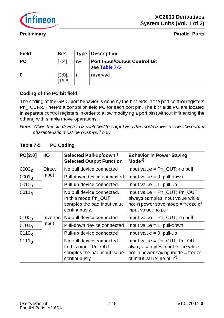
XC2000 DerivativesSystem Units (Vol. 1 of 2)
Parallel PortsPreliminary
Coding of the PC bit fieldThe coding of the GPIO port behavior is done by the bit fields in the port control registersPn_IOCRx. There’s a control bit field PC for each port pin. The bit fields PC are locatedin separate control registers in order to allow modifying a port pin (without influencing theothers) with simple move operations.Note: When the pin direction is switched to output and the mode is test mode, the output
characteristic must be push-pull only.
Field Bits Type DescriptionPC [7:4] rw Port Input/Output Control Bit
see Table 7-50 [3:0],
[15:8]r reserved
Table 7-5 PC Coding
PC[3:0] I/O Selected Pull-up/down /Selected Output Function
Behavior in Power Saving Mode1)
0000B Direct Input
No pull device connected Input value = Pn_OUT; no pull0001B Pull-down device connected Input value = 0; pull-down0010B Pull-up device connected Input value = 1; pull-up0011B No pull device connected.
In this mode Pn_OUT samples the pad input value continuously.
Input value = Pn_OUT; Pn_OUT always samples input value while not in power save mode = freeze of input value; no pull
0100B Inverted Input
No pull device connected Input value = Pn_OUT; no pull0101B Pull-down device connected Input value = 1; pull-down0110B Pull-up device connected Input value = 0; pull-up0111B No pull device connected
In this mode Pn_OUT samples the pad input value continuously.
Input value = Pn_OUT; Pn_OUT always samples input value while not in power saving mode = freeze of input value; no pull2)
User’s Manual 7-15 V1.0, 2007-06Parallel Ports, V1.6D4
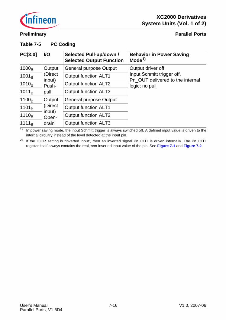
XC2000 DerivativesSystem Units (Vol. 1 of 2)
Parallel PortsPreliminary
1000B Output(Direct input)Push-pull
General purpose Output Output driver off.Input Schmitt trigger off.Pn_OUT delivered to the internal logic; no pull
1001B Output function ALT11010B Output function ALT21011B Output function ALT3
1100B Output(Direct input)Open-drain
General purpose Output1101B Output function ALT11110B Output function ALT21111B Output function ALT31) In power saving mode, the input Schmitt trigger is always switched off. A defined input value is driven to the
internal circuitry instead of the level detected at the input pin.2) If the IOCR setting is “inverted input”, then an inverted signal Pn_OUT is driven internally. The Pn_OUT
register itself always contains the real, non-inverted input value of the pin. See Figure 7-1 and Figure 7-2.
Table 7-5 PC Coding
PC[3:0] I/O Selected Pull-up/down /Selected Output Function
Behavior in Power Saving Mode1)
User’s Manual 7-16 V1.0, 2007-06Parallel Ports, V1.6D4
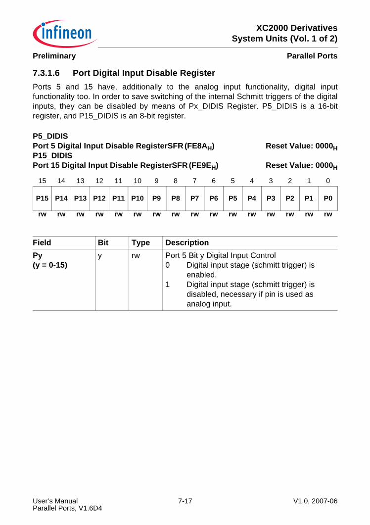
XC2000 DerivativesSystem Units (Vol. 1 of 2)
Parallel PortsPreliminary
7.3.1.6 Port Digital Input Disable RegisterPorts 5 and 15 have, additionally to the analog input functionality, digital inputfunctionality too. In order to save switching of the internal Schmitt triggers of the digitalinputs, they can be disabled by means of Px_DIDIS Register. P5_DIDIS is a 16-bitregister, and P15_DIDIS is an 8-bit register.
P5_DIDIS Port 5 Digital Input Disable RegisterSFR (FE8AH) Reset Value: 0000HP15_DIDIS Port 15 Digital Input Disable RegisterSFR (FE9EH) Reset Value: 0000H
15 14 13 12 11 10 9 8 7 6 5 4 3 2 1 0
P15 P14 P13 P12 P11 P10 P9 P8 P7 P6 P5 P4 P3 P2 P1 P0
rw rw rw rw rw rw rw rw rw rw rw rw rw rw rw rw
Field Bit Type DescriptionPy(y = 0-15)
y rw Port 5 Bit y Digital Input Control0 Digital input stage (schmitt trigger) is
enabled.1 Digital input stage (schmitt trigger) is
disabled, necessary if pin is used as analog input.
User’s Manual 7-17 V1.0, 2007-06Parallel Ports, V1.6D4

XC2000 DerivativesSystem Units (Vol. 1 of 2)
Parallel PortsPreliminary
7.3.2 Port 0Port 0 is an 8-bit GPIO port.
7.3.2.1 Overview The port registers of Port 0 are shown in Figure 7-4.For this port, all pins can be read as GPIO, from the Port Input Register.
Figure 7-4 Port 0 Register Overview
Table 7-6 Port 0 RegistersRegister Short Name
Register Long Name Address Offset
Reset Value
P0_OUT Port 0 Output Register FFA2H 0000H
P0_IN Port 0 Input Register FF80H 0000H
P0_OMRL Port 0 Output Modification Register Low E9C0H 0000H
P0_POCON Port 0 Output Control Register E8A0H 0000H
P0_IOCR00 Port 0 Input/Output Control Register 0 E800H 0000H
P0_IOCR01 Port 0 Input/Output Control Register 1 E802H 0000H
P0_IOCR02 Port 0 Input/Output Control Register 2 E804H 0000H
P0_IOCR03 Port 0 Input/Output Control Register 3 E806H 0000H
P0_IOCR04 Port 0 Input/Output Control Register 4 E808H 0000H
P0_IOCR05 Port 0 Input/Output Control Register 5 E80AH 0000H
P0_IOCR06 Port 0 Input/Output Control Register 6 E80CH 0000H
P0_IOCR07 Port 0 Input/Output Control Register 7 E80EH 0000H
P0_OMRL
Port0_Regs.vsd
P0_IOCR00 P0_OUT
ModificationRegisters
DataRegisters
P0_IN
ControlRegisters
P0_IOCR07:
P0_POCON
User’s Manual 7-18 V1.0, 2007-06Parallel Ports, V1.6D4
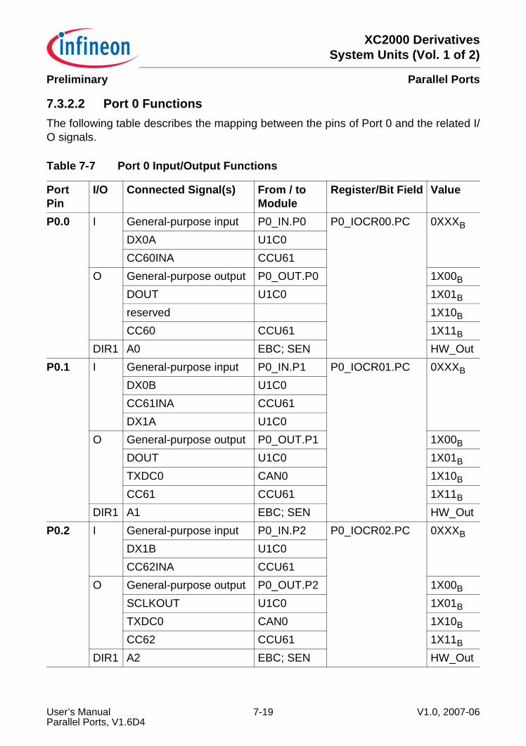
XC2000 DerivativesSystem Units (Vol. 1 of 2)
Parallel PortsPreliminary
7.3.2.2 Port 0 FunctionsThe following table describes the mapping between the pins of Port 0 and the related I/O signals.
Table 7-7 Port 0 Input/Output Functions
PortPin
I/O Connected Signal(s) From / to Module
Register/Bit Field Value
P0.0 I General-purpose input P0_IN.P0 P0_IOCR00.PC 0XXXB
DX0A U1C0CC60INA CCU61
O General-purpose output P0_OUT.P0 1X00B
DOUT U1C0 1X01B
reserved 1X10B
CC60 CCU61 1X11B
DIR1 A0 EBC; SEN HW_OutP0.1 I General-purpose input P0_IN.P1 P0_IOCR01.PC 0XXXB
DX0B U1C0CC61INA CCU61DX1A U1C0
O General-purpose output P0_OUT.P1 1X00B
DOUT U1C0 1X01B
TXDC0 CAN0 1X10B
CC61 CCU61 1X11B
DIR1 A1 EBC; SEN HW_OutP0.2 I General-purpose input P0_IN.P2 P0_IOCR02.PC 0XXXB
DX1B U1C0CC62INA CCU61
O General-purpose output P0_OUT.P2 1X00B
SCLKOUT U1C0 1X01B
TXDC0 CAN0 1X10B
CC62 CCU61 1X11B
DIR1 A2 EBC; SEN HW_Out
User’s Manual 7-19 V1.0, 2007-06Parallel Ports, V1.6D4
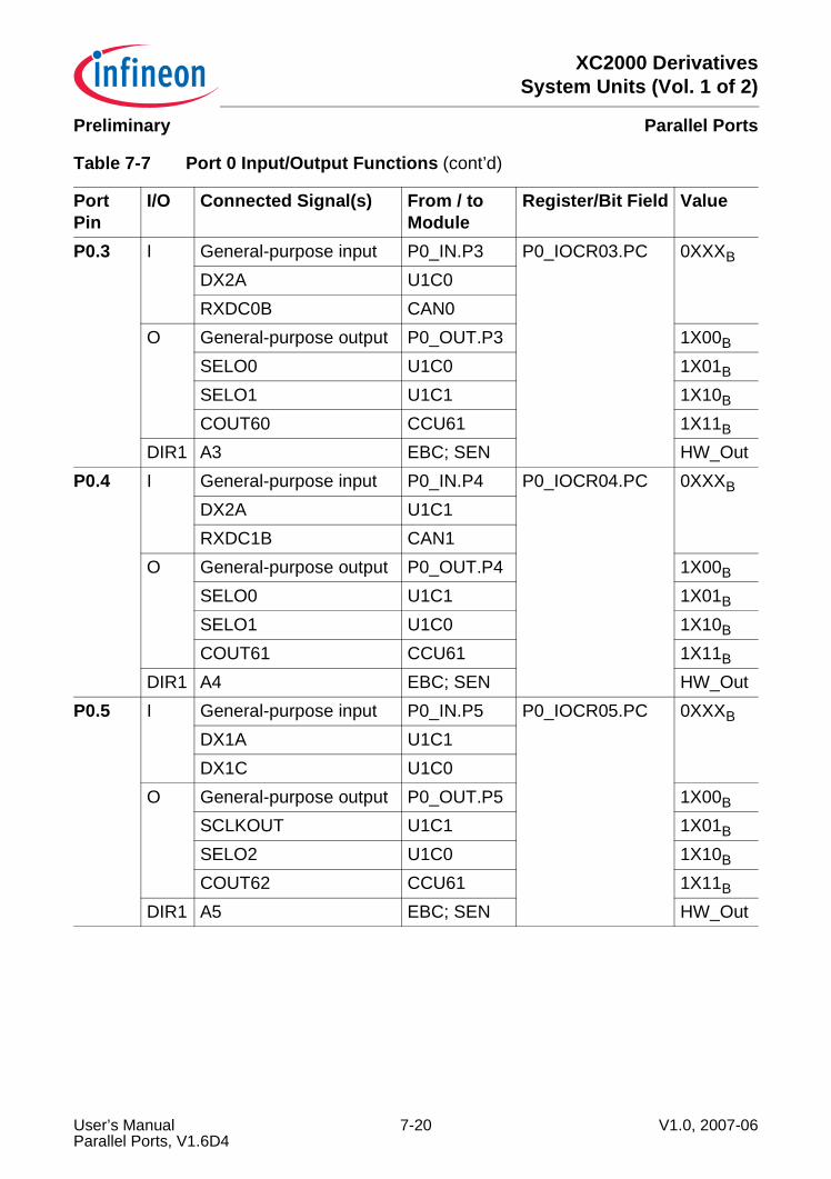
XC2000 DerivativesSystem Units (Vol. 1 of 2)
Parallel PortsPreliminary
P0.3 I General-purpose input P0_IN.P3 P0_IOCR03.PC 0XXXB
DX2A U1C0RXDC0B CAN0
O General-purpose output P0_OUT.P3 1X00B
SELO0 U1C0 1X01B
SELO1 U1C1 1X10B
COUT60 CCU61 1X11B
DIR1 A3 EBC; SEN HW_OutP0.4 I General-purpose input P0_IN.P4 P0_IOCR04.PC 0XXXB
DX2A U1C1RXDC1B CAN1
O General-purpose output P0_OUT.P4 1X00B
SELO0 U1C1 1X01B
SELO1 U1C0 1X10B
COUT61 CCU61 1X11B
DIR1 A4 EBC; SEN HW_OutP0.5 I General-purpose input P0_IN.P5 P0_IOCR05.PC 0XXXB
DX1A U1C1DX1C U1C0
O General-purpose output P0_OUT.P5 1X00B
SCLKOUT U1C1 1X01B
SELO2 U1C0 1X10B
COUT62 CCU61 1X11B
DIR1 A5 EBC; SEN HW_Out
Table 7-7 Port 0 Input/Output Functions (cont’d)
PortPin
I/O Connected Signal(s) From / to Module
Register/Bit Field Value
User’s Manual 7-20 V1.0, 2007-06Parallel Ports, V1.6D4
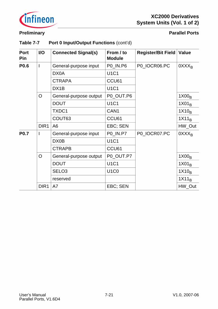
XC2000 DerivativesSystem Units (Vol. 1 of 2)
Parallel PortsPreliminary
P0.6 I General-purpose input P0_IN.P6 P0_IOCR06.PC 0XXXB
DX0A U1C1CTRAPA CCU61DX1B U1C1
O General-purpose output P0_OUT.P6 1X00B
DOUT U1C1 1X01B
TXDC1 CAN1 1X10B
COUT63 CCU61 1X11B
DIR1 A6 EBC; SEN HW_OutP0.7 I General-purpose input P0_IN.P7 P0_IOCR07.PC 0XXXB
DX0B U1C1CTRAPB CCU61
O General-purpose output P0_OUT.P7 1X00B
DOUT U1C1 1X01B
SELO3 U1C0 1X10B
reserved 1X11B
DIR1 A7 EBC; SEN HW_Out
Table 7-7 Port 0 Input/Output Functions (cont’d)
PortPin
I/O Connected Signal(s) From / to Module
Register/Bit Field Value
User’s Manual 7-21 V1.0, 2007-06Parallel Ports, V1.6D4
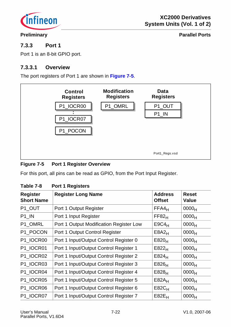
XC2000 DerivativesSystem Units (Vol. 1 of 2)
Parallel PortsPreliminary
7.3.3 Port 1Port 1 is an 8-bit GPIO port.
7.3.3.1 OverviewThe port registers of Port 1 are shown in Figure 7-5.
Figure 7-5 Port 1 Register Overview
For this port, all pins can be read as GPIO, from the Port Input Register.
Table 7-8 Port 1 RegistersRegister Short Name
Register Long Name Address Offset
Reset Value
P1_OUT Port 1 Output Register FFA4H 0000H
P1_IN Port 1 Input Register FF82H 0000H
P1_OMRL Port 1 Output Modification Register Low E9C4H 0000H
P1_POCON Port 1 Output Control Register E8A2H 0000H
P1_IOCR00 Port 1 Input/Output Control Register 0 E820H 0000H
P1_IOCR01 Port 1 Input/Output Control Register 1 E822H 0000H
P1_IOCR02 Port 1 Input/Output Control Register 2 E824H 0000H
P1_IOCR03 Port 1 Input/Output Control Register 3 E826H 0000H
P1_IOCR04 Port 1 Input/Output Control Register 4 E828H 0000H
P1_IOCR05 Port 1 Input/Output Control Register 5 E82AH 0000H
P1_IOCR06 Port 1 Input/Output Control Register 6 E82CH 0000H
P1_IOCR07 Port 1 Input/Output Control Register 7 E82EH 0000H
P1_OMRL
Port1_Regs.vsd
P1_IOCR00 P1_OUT
ModificationRegisters
DataRegisters
P1_IN
ControlRegisters
P1_IOCR07:
P1_POCON
User’s Manual 7-22 V1.0, 2007-06Parallel Ports, V1.6D4

XC2000 DerivativesSystem Units (Vol. 1 of 2)
Parallel PortsPreliminary
7.3.3.2 Port 1 FunctionsThe following table describes the mapping between the pins of Port 1 and the related I/O signals.
Table 7-9 Port 1 Input/Output Functions
PortPin
I/O Connected Signal(s) From / to Module
Register/Bit Field Value
P1.0 I General-purpose input P1_IN.P0 P1_IOCR00.PC 0XXXB
ERU_0B0 SCUCTRAPB CCU62
O General-purpose output P1_OUT.P0 1X00B
MCLKOUT U1C0 1X01B
SELO4 U1C0 1X10B
reserved 1X11B
DIR1 A8 EBC; SEN HW_OutP1.1 I General-purpose input P1_IN.P1 P1_IOCR01.PC 0XXXB
ERU_1B0 SCUDX0C U2C1
O General-purpose output P1_OUT.P1 1X00B
COUT62 CCU62 1X01B
SELO5 U1C0 1X10B
DOUT U2C1 1X11B
DIR1 A9 EBC; SEN HW_Out
User’s Manual 7-23 V1.0, 2007-06Parallel Ports, V1.6D4
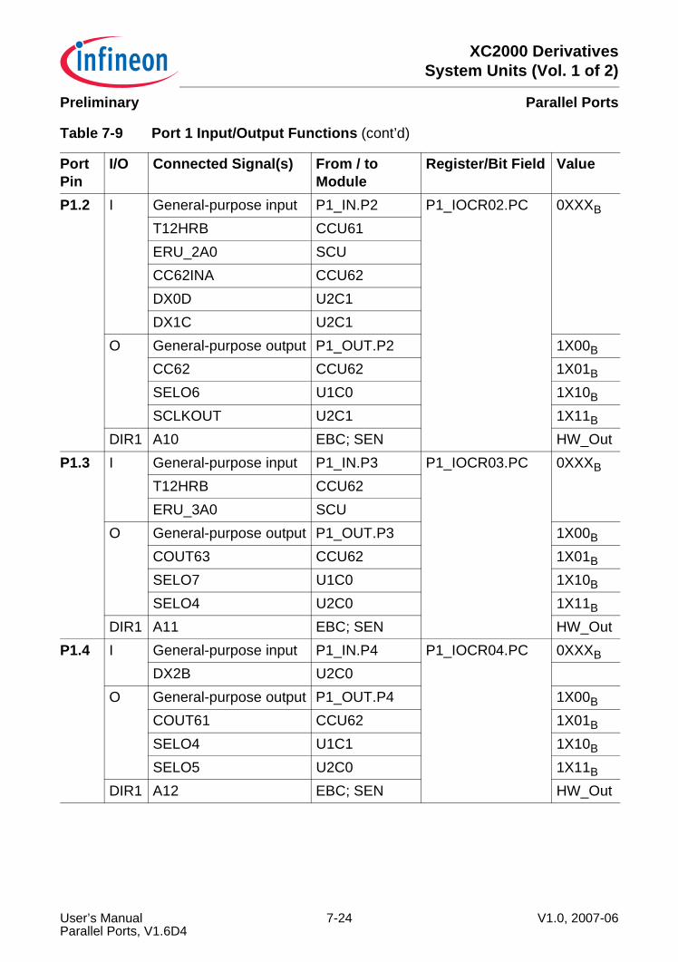
XC2000 DerivativesSystem Units (Vol. 1 of 2)
Parallel PortsPreliminary
P1.2 I General-purpose input P1_IN.P2 P1_IOCR02.PC 0XXXB
T12HRB CCU61ERU_2A0 SCUCC62INA CCU62DX0D U2C1DX1C U2C1
O General-purpose output P1_OUT.P2 1X00B
CC62 CCU62 1X01B
SELO6 U1C0 1X10B
SCLKOUT U2C1 1X11B
DIR1 A10 EBC; SEN HW_OutP1.3 I General-purpose input P1_IN.P3 P1_IOCR03.PC 0XXXB
T12HRB CCU62ERU_3A0 SCU
O General-purpose output P1_OUT.P3 1X00B
COUT63 CCU62 1X01B
SELO7 U1C0 1X10B
SELO4 U2C0 1X11B
DIR1 A11 EBC; SEN HW_OutP1.4 I General-purpose input P1_IN.P4 P1_IOCR04.PC 0XXXB
DX2B U2C0O General-purpose output P1_OUT.P4 1X00B
COUT61 CCU62 1X01B
SELO4 U1C1 1X10B
SELO5 U2C0 1X11B
DIR1 A12 EBC; SEN HW_Out
Table 7-9 Port 1 Input/Output Functions (cont’d)
PortPin
I/O Connected Signal(s) From / to Module
Register/Bit Field Value
User’s Manual 7-24 V1.0, 2007-06Parallel Ports, V1.6D4
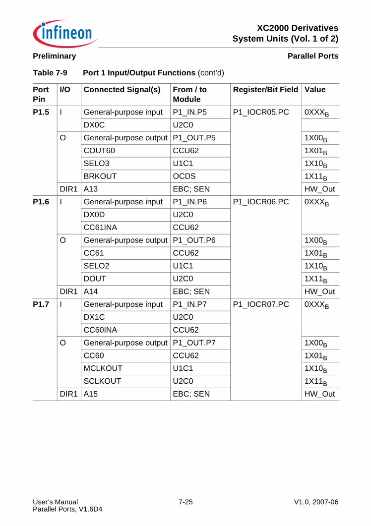
XC2000 DerivativesSystem Units (Vol. 1 of 2)
Parallel PortsPreliminary
P1.5 I General-purpose input P1_IN.P5 P1_IOCR05.PC 0XXXB
DX0C U2C0O General-purpose output P1_OUT.P5 1X00B
COUT60 CCU62 1X01B
SELO3 U1C1 1X10B
BRKOUT OCDS 1X11B
DIR1 A13 EBC; SEN HW_OutP1.6 I General-purpose input P1_IN.P6 P1_IOCR06.PC 0XXXB
DX0D U2C0CC61INA CCU62
O General-purpose output P1_OUT.P6 1X00B
CC61 CCU62 1X01B
SELO2 U1C1 1X10B
DOUT U2C0 1X11B
DIR1 A14 EBC; SEN HW_OutP1.7 I General-purpose input P1_IN.P7 P1_IOCR07.PC 0XXXB
DX1C U2C0CC60INA CCU62
O General-purpose output P1_OUT.P7 1X00B
CC60 CCU62 1X01B
MCLKOUT U1C1 1X10B
SCLKOUT U2C0 1X11B
DIR1 A15 EBC; SEN HW_Out
Table 7-9 Port 1 Input/Output Functions (cont’d)
PortPin
I/O Connected Signal(s) From / to Module
Register/Bit Field Value
User’s Manual 7-25 V1.0, 2007-06Parallel Ports, V1.6D4
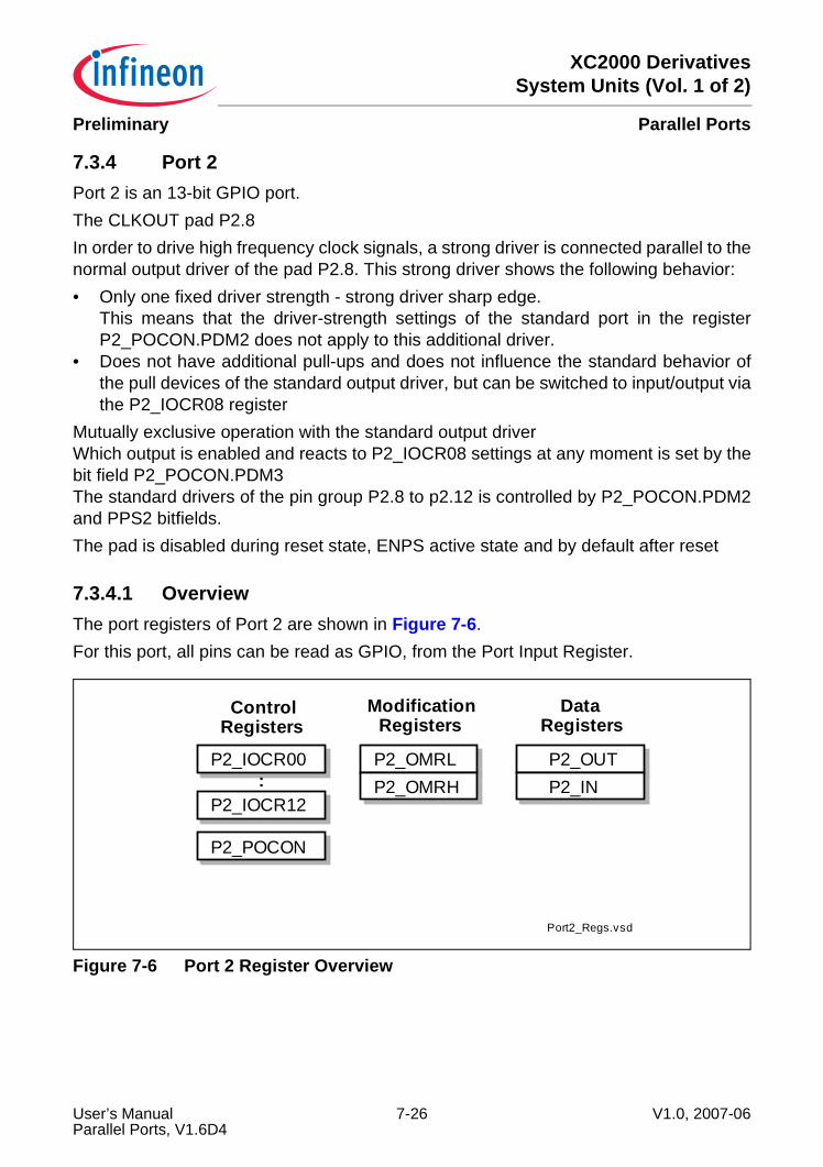
XC2000 DerivativesSystem Units (Vol. 1 of 2)
Parallel PortsPreliminary
7.3.4 Port 2Port 2 is an 13-bit GPIO port.The CLKOUT pad P2.8In order to drive high frequency clock signals, a strong driver is connected parallel to thenormal output driver of the pad P2.8. This strong driver shows the following behavior:• Only one fixed driver strength - strong driver sharp edge.
This means that the driver-strength settings of the standard port in the registerP2_POCON.PDM2 does not apply to this additional driver.
• Does not have additional pull-ups and does not influence the standard behavior ofthe pull devices of the standard output driver, but can be switched to input/output viathe P2_IOCR08 register
Mutually exclusive operation with the standard output driverWhich output is enabled and reacts to P2_IOCR08 settings at any moment is set by thebit field P2_POCON.PDM3 The standard drivers of the pin group P2.8 to p2.12 is controlled by P2_POCON.PDM2and PPS2 bitfields.The pad is disabled during reset state, ENPS active state and by default after reset
7.3.4.1 OverviewThe port registers of Port 2 are shown in Figure 7-6.For this port, all pins can be read as GPIO, from the Port Input Register.
Figure 7-6 Port 2 Register Overview
P2_OMRL
Port2_Regs.vsd
P2_IOCR00 P2_OUT
ModificationRegisters
DataRegisters
P2_IN
ControlRegisters
P2_IOCR12:
P2_POCON
P2_OMRH
User’s Manual 7-26 V1.0, 2007-06Parallel Ports, V1.6D4
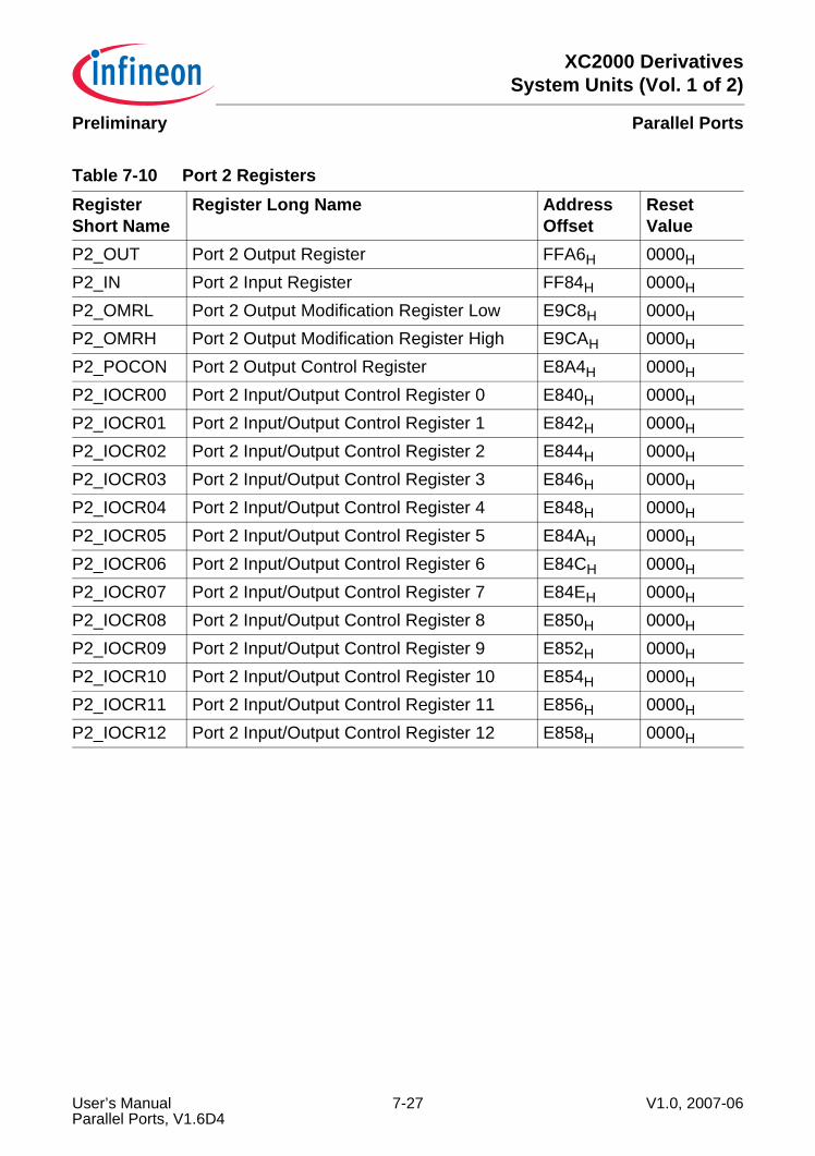
XC2000 DerivativesSystem Units (Vol. 1 of 2)
Parallel PortsPreliminary
Table 7-10 Port 2 RegistersRegister Short Name
Register Long Name Address Offset
Reset Value
P2_OUT Port 2 Output Register FFA6H 0000H
P2_IN Port 2 Input Register FF84H 0000H
P2_OMRL Port 2 Output Modification Register Low E9C8H 0000H
P2_OMRH Port 2 Output Modification Register High E9CAH 0000H
P2_POCON Port 2 Output Control Register E8A4H 0000H
P2_IOCR00 Port 2 Input/Output Control Register 0 E840H 0000H
P2_IOCR01 Port 2 Input/Output Control Register 1 E842H 0000H
P2_IOCR02 Port 2 Input/Output Control Register 2 E844H 0000H
P2_IOCR03 Port 2 Input/Output Control Register 3 E846H 0000H
P2_IOCR04 Port 2 Input/Output Control Register 4 E848H 0000H
P2_IOCR05 Port 2 Input/Output Control Register 5 E84AH 0000H
P2_IOCR06 Port 2 Input/Output Control Register 6 E84CH 0000H
P2_IOCR07 Port 2 Input/Output Control Register 7 E84EH 0000H
P2_IOCR08 Port 2 Input/Output Control Register 8 E850H 0000H
P2_IOCR09 Port 2 Input/Output Control Register 9 E852H 0000H
P2_IOCR10 Port 2 Input/Output Control Register 10 E854H 0000H
P2_IOCR11 Port 2 Input/Output Control Register 11 E856H 0000H
P2_IOCR12 Port 2 Input/Output Control Register 12 E858H 0000H
User’s Manual 7-27 V1.0, 2007-06Parallel Ports, V1.6D4
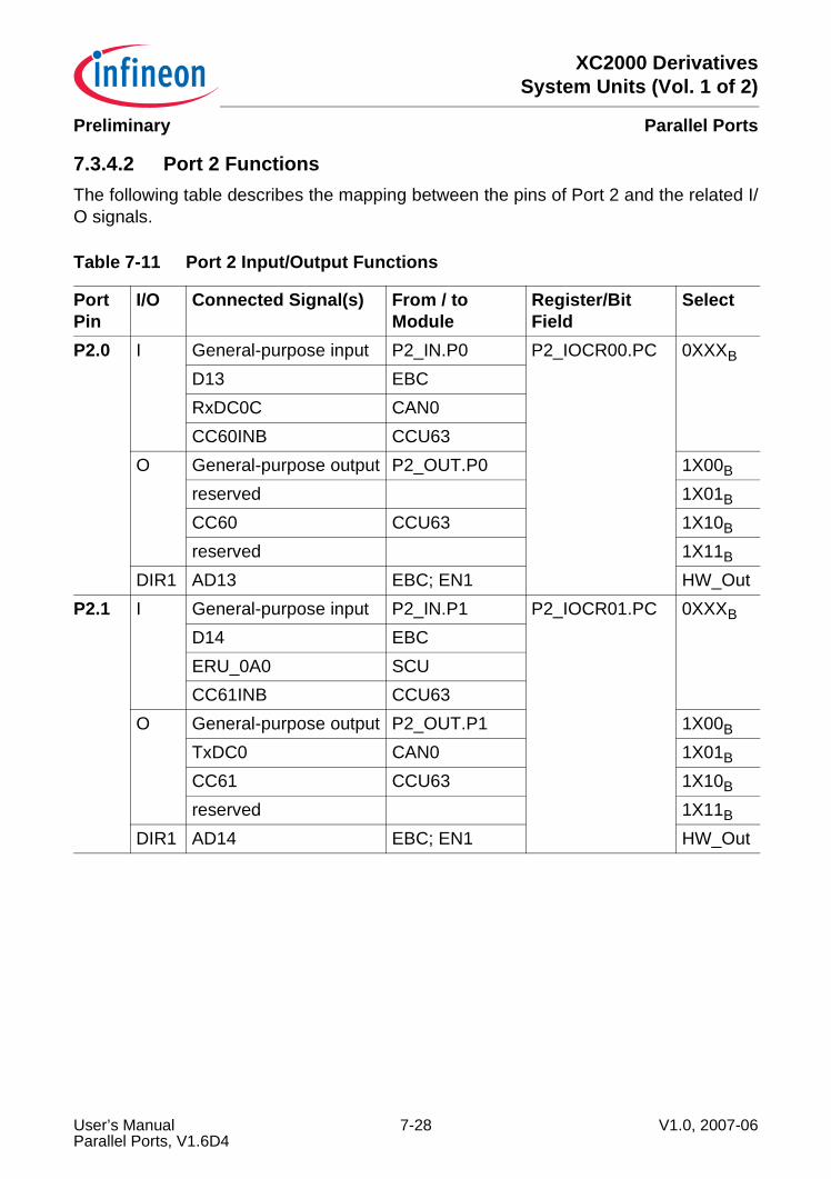
XC2000 DerivativesSystem Units (Vol. 1 of 2)
Parallel PortsPreliminary
7.3.4.2 Port 2 FunctionsThe following table describes the mapping between the pins of Port 2 and the related I/O signals.
Table 7-11 Port 2 Input/Output Functions
PortPin
I/O Connected Signal(s) From / to Module
Register/Bit Field
Select
P2.0 I General-purpose input P2_IN.P0 P2_IOCR00.PC 0XXXB
D13 EBCRxDC0C CAN0CC60INB CCU63
O General-purpose output P2_OUT.P0 1X00B
reserved 1X01B
CC60 CCU63 1X10B
reserved 1X11B
DIR1 AD13 EBC; EN1 HW_OutP2.1 I General-purpose input P2_IN.P1 P2_IOCR01.PC 0XXXB
D14 EBCERU_0A0 SCUCC61INB CCU63
O General-purpose output P2_OUT.P1 1X00B
TxDC0 CAN0 1X01B
CC61 CCU63 1X10B
reserved 1X11B
DIR1 AD14 EBC; EN1 HW_Out
User’s Manual 7-28 V1.0, 2007-06Parallel Ports, V1.6D4

XC2000 DerivativesSystem Units (Vol. 1 of 2)
Parallel PortsPreliminary
P2.2 I General-purpose input P2_IN.P2 P2_IOCR02.PC 0XXXB
D15 EBCECTT1 CAN0 TTCANERU_1A0 SCUCC62INB CCU63
O General-purpose output P2_OUT.P2 1X00B
TxDC1 CAN1 1X01B
CC62 CCU63 1X10B
reserved 1X11B
DIR1 AD15 EBC; EN1 HW_OutP2.3 I General-purpose input P2_IN.P3 P2_IOCR03.PC 0XXXB
DX0E U0C0RXDC0A CAN0CC2_16 CAPCOM2
O General-purpose output P2_OUT.P3 1X00B
DOUT U0C0 1X01B
COUT63 CCU63 1X10B
CC2_16 CAPCOM2 1X11B
DIR2 A16 EBC; SEN HW_OutP2.4 I General-purpose input P2_IN.P4 P2_IOCR04.PC 0XXXB
DX0F U0C0RXDC1A CAN1CC2_17 CAPCOM2
O General-purpose output P2_OUT.P4 1X00B
reserved 1X01B
TXDC0 CAN0 1X10B
CC2_17 CAPCOM2 1X11B
DIR2 A17 EBC; SEN HW_Out
Table 7-11 Port 2 Input/Output Functions (cont’d)
PortPin
I/O Connected Signal(s) From / to Module
Register/Bit Field
Select
User’s Manual 7-29 V1.0, 2007-06Parallel Ports, V1.6D4
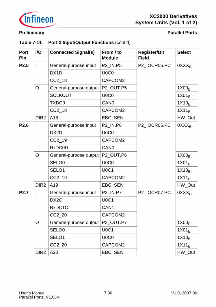
XC2000 DerivativesSystem Units (Vol. 1 of 2)
Parallel PortsPreliminary
P2.5 I General-purpose input P2_IN.P5 P2_IOCR05.PC 0XXXB
DX1D U0C0CC2_18 CAPCOM2
O General-purpose output P2_OUT.P5 1X00B
SCLKOUT U0C0 1X01B
TXDC0 CAN0 1X10B
CC2_18 CAPCOM2 1X11B
DIR2 A18 EBC; SEN HW_OutP2.6 I General-purpose input P2_IN.P6 P2_IOCR06.PC 0XXXB
DX2D U0C0CC2_19 CAPCOM2RxDC0D CAN0
O General-purpose output P2_OUT.P6 1X00B
SELO0 U0C0 1X01B
SELO1 U0C1 1X10B
CC2_19 CAPCOM2 1X11B
DIR2 A19 EBC; SEN HW_OutP2.7 I General-purpose input P2_IN.P7 P2_IOCR07.PC 0XXXB
DX2C U0C1RxDC1C CAN1CC2_20 CAPCOM2
O General-purpose output P2_OUT.P7 1X00B
SELO0 U0C1 1X01B
SELO1 U0C0 1X10B
CC2_20 CAPCOM2 1X11B
DIR2 A20 EBC; SEN HW_Out
Table 7-11 Port 2 Input/Output Functions (cont’d)
PortPin
I/O Connected Signal(s) From / to Module
Register/Bit Field
Select
User’s Manual 7-30 V1.0, 2007-06Parallel Ports, V1.6D4
XC2000 DerivativesSystem Units (Vol. 1 of 2)
Parallel PortsPreliminary
P2.8 I General-purpose input P2_IN.P8 P2_IOCR08.PC 0XXXB
DX1D U0C1CC2_21 CAPCOM2
O General-purpose output P2_OUT.P8 1X00B
SCLKOUT U0C1 1X01B
FOUT SCU 1X10B
CC2_21 CAPCOM2 1X11B
DIR2 A21 EBC; SEN HW_OutP2.9 I General-purpose input P2_IN.P9 P2_IOCR09.PC 0XXXB
TCK_A JTAGCC2_22 CAPCOM2
O General-purpose output P2_OUT.P9 1X00B
DOUT U0C1 1X01B
TXDC1 CAN1 1X10B
CC2_22 CAPCOM2 1X11B
SDIR A22 EBC; SEN HW_OutP2.10 I General-purpose input P2_IN.P10 P2_IOCR10.PC 0XXXB
DX0E U0C1CC2_23 CAPCOM2CAPIN GPT12E
O General-purpose output P2_OUT.P10 1X00B
DOUT U0C1 1X01B
SELO3 U0C0 1X10B
CC2_23 CAPCOM2 1X11B
DIR2 A23 EBC; SEN HW_Out
Table 7-11 Port 2 Input/Output Functions (cont’d)
PortPin
I/O Connected Signal(s) From / to Module
Register/Bit Field
Select
User’s Manual 7-31 V1.0, 2007-06Parallel Ports, V1.6D4

XC2000 DerivativesSystem Units (Vol. 1 of 2)
Parallel PortsPreliminary
P2.11 I General-purpose input P2_IN.P11 P2_IOCR11.PC 0XXXB
O General-purpose output P2_OUT.P11 1X00B
SELO2 U0C0 1X01B
SELO2 U0C1 1X10B
reserved 1X11B
SDIR BHE EBC; SEN HW_OutP2.12 I General-purpose input P2_IN.P12 P2_IOCR12.PC 0XXXB
READY EBCO General-purpose output P2_OUT.P12 1X00B
SELO4 U0C0 1X01B
SELO3 U0C1 1X10B
reserved 1X11B
SDIR READY EBC; SEN HW_Out
Table 7-11 Port 2 Input/Output Functions (cont’d)
PortPin
I/O Connected Signal(s) From / to Module
Register/Bit Field
Select
User’s Manual 7-32 V1.0, 2007-06Parallel Ports, V1.6D4

XC2000 DerivativesSystem Units (Vol. 1 of 2)
Parallel PortsPreliminary
7.3.5 Port 3Port 3 is an 8-bit GPIO port.
7.3.5.1 OverviewThe port registers of Port 3 are shown in Figure 7-7.For this port, all pins can be read as GPIO, from the Port Input Register.
Figure 7-7 Port 3 Register Overview
Table 7-12 Port 3 RegistersRegister Short Name
Register Long Name Address Offset
Reset Value
P3_OUT Port 3 Output Register FFA8H 0000H
P3_IN Port 3 Input Register FF86H 0000H
P3_OMRL Port 3 Output Modification Register Low E9CCH 0000H
P3_POCON Port 3 Output Control Register E8A6H 0000H
P3_IOCR00 Port 3 Input/Output Control Register 0 E860H 0000H
P3_IOCR01 Port 3 Input/Output Control Register 1 E862H 0000H
P3_IOCR02 Port 3 Input/Output Control Register 2 E864H 0000H
P3_IOCR03 Port 3 Input/Output Control Register 3 E866H 0000H
P3_IOCR04 Port 3 Input/Output Control Register 4 E868H 0000H
P3_IOCR05 Port 3 Input/Output Control Register 5 E86AH 0000H
P3_IOCR06 Port 3 Input/Output Control Register 6 E86CH 0000H
P3_IOCR07 Port 3 Input/Output Control Register 7 E86EH 0000H
P3_OMRL
Port3_Regs.vsd
P3_IOCR00 P3_OUT
ModificationRegisters
DataRegisters
P3_IN
ControlRegisters
P3_IOCR07:
P3_POCON
User’s Manual 7-33 V1.0, 2007-06Parallel Ports, V1.6D4
XC2000 DerivativesSystem Units (Vol. 1 of 2)
Parallel PortsPreliminary
7.3.5.2 Port 3 FunctionsThe following table describes the mapping between the pins of Port 3 and the related I/O signals.
Table 7-13 Port 3 Input/Output Functions
PortPin
I/O Connected Signal(s) From / to Module
Register/Bit Field
Select
P3.0 I General-purpose input P3_IN.P0 P3_IOCR00.PC 0XXXB
DX0A U2C0RxDC3B CAN3DX1A U2C0
O General-purpose output P3_OUT.P0 1X00B
DOUT U2C0 1X01B
reserved 1X10B
reserved 1X11B
SDIR BREQ EBC; EN3 HW_OutP3.1 I General-purpose input P3_IN.P1 P3_IOCR01.PC 0XXXB
DX0B U2C0HLDA EBC
O General-purpose output P3_OUT.P1 1X00B
DOUT U2C0 1X01B
TXDC3 CAN3 1X10B
reserved 1X11B
SDIR HLDA EBC; EN3 HW_OutP3.2 I General-purpose input P3_IN.P2 P3_IOCR02.PC 0XXXB
DX1B U2C0HOLD EBC
O General-purpose output P3_OUT.P2 1X00B
SCLKOUT U2C0 1X01B
TXDC3 CAN3 1X10B
reserved 1X11B
User’s Manual 7-34 V1.0, 2007-06Parallel Ports, V1.6D4
XC2000 DerivativesSystem Units (Vol. 1 of 2)
Parallel PortsPreliminary
P3.3 I General-purpose input P3_IN.P3 P3_IOCR03.PC 0XXXB
DX2A U2C0RXDC3A CAN3
O General-purpose output P3_OUT.P3 1X00B
SELO0 U2C0 1X01B
SELO1 U2C1 1X10B
reserved 1X11B
P3.4 I General-purpose input P3_IN.P4 P3_IOCR04.PC 0XXXB
DX2A U2C1RXDC4A CAN4
O General-purpose output P3_OUT.P4 1X00B
SELO0 U2C1 1X01B
SELO1 U2C0 1X10B
SELO4 U0C0 1X11B
P3.5 I General-purpose input P3_IN.P5 P3_IOCR05.PC 0XXXB
DX1A U2C1O General-purpose output P3_OUT.P5 1X00B
SCLKOUT U2C1 1X01B
SELO2 U2C0 1X10B
SELO5 U0C0 1X11B
P3.6 I General-purpose input P3_IN.P6 P3_IOCR06.PC 0XXXB
DX0A U2C1DX1B U2C1
O General-purpose output P3_OUT.P6 1X00B
DOUT U2C1 1X01B
TXDC4 CAN4 1X10B
SELO6 U0C0 1X11B
Table 7-13 Port 3 Input/Output Functions (cont’d)
PortPin
I/O Connected Signal(s) From / to Module
Register/Bit Field
Select
User’s Manual 7-35 V1.0, 2007-06Parallel Ports, V1.6D4
XC2000 DerivativesSystem Units (Vol. 1 of 2)
Parallel PortsPreliminary
P3.7 I General-purpose input P3_IN.P7 P3_IOCR07.PC 0XXXB
DX0B U2C1O General-purpose output P3_OUT.P7 1X00B
DOUT U2C1 1X01B
SELO3 U2C0 1X10B
SELO7 U0C0 1X11B
Table 7-13 Port 3 Input/Output Functions (cont’d)
PortPin
I/O Connected Signal(s) From / to Module
Register/Bit Field
Select
User’s Manual 7-36 V1.0, 2007-06Parallel Ports, V1.6D4
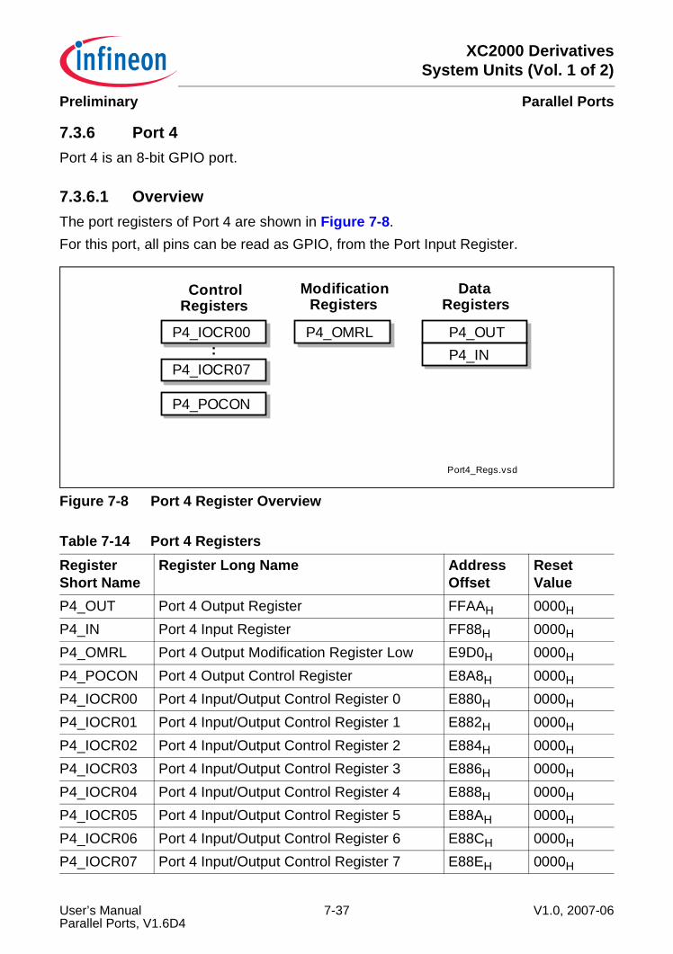
XC2000 DerivativesSystem Units (Vol. 1 of 2)
Parallel PortsPreliminary
7.3.6 Port 4Port 4 is an 8-bit GPIO port.
7.3.6.1 OverviewThe port registers of Port 4 are shown in Figure 7-8.For this port, all pins can be read as GPIO, from the Port Input Register.
Figure 7-8 Port 4 Register Overview
Table 7-14 Port 4 RegistersRegister Short Name
Register Long Name Address Offset
Reset Value
P4_OUT Port 4 Output Register FFAAH 0000H
P4_IN Port 4 Input Register FF88H 0000H
P4_OMRL Port 4 Output Modification Register Low E9D0H 0000H
P4_POCON Port 4 Output Control Register E8A8H 0000H
P4_IOCR00 Port 4 Input/Output Control Register 0 E880H 0000H
P4_IOCR01 Port 4 Input/Output Control Register 1 E882H 0000H
P4_IOCR02 Port 4 Input/Output Control Register 2 E884H 0000H
P4_IOCR03 Port 4 Input/Output Control Register 3 E886H 0000H
P4_IOCR04 Port 4 Input/Output Control Register 4 E888H 0000H
P4_IOCR05 Port 4 Input/Output Control Register 5 E88AH 0000H
P4_IOCR06 Port 4 Input/Output Control Register 6 E88CH 0000H
P4_IOCR07 Port 4 Input/Output Control Register 7 E88EH 0000H
P4_OMRL
Port4_Regs.vsd
P4_IOCR00 P4_OUT
ModificationRegisters
DataRegisters
P4_IN
ControlRegisters
P4_IOCR07:
P4_POCON
User’s Manual 7-37 V1.0, 2007-06Parallel Ports, V1.6D4
XC2000 DerivativesSystem Units (Vol. 1 of 2)
Parallel PortsPreliminary
7.3.6.2 Port 4 FunctionsThe following table describes the mapping between the pins of Port 4 and the related I/O signals.
Table 7-15 Port 4 Input/Output Functions
PortPin
I/O Connected Signal(s) From / to Module
Register/Bit Field
Select
P4.0 I General-purpose input P4_IN.P0 P4_IOCR00.PC 0XXXB
CC2_24 CAPCOM2O General-purpose output P4_OUT.P0 1X00B
reserved 1X01B
reserved 1X10B
CC2_24 CAPCOM2 1X11B
DIR3 CS0 EBC; SEN HW_OutP4.1 I General-purpose input P4_IN.P1 P4_IOCR01.PC 0XXXB
CC2_25 CAPCOM2O General-purpose output P4_OUT.P1 1X00B
reserved 1X01B
TXDC2 CAN2 1X10B
CC2_25 CAPCOM2 1X11B
DIR3 CS1 EBC; SEN HW_OutP4.2 I General-purpose input P4_IN.P2 P4_IOCR02.PC 0XXXB
CC2_26 CAPCOM2T2IN GPT12E
O General-purpose output P4_OUT.P2 1X00B
reserved 1X01B
TXDC2 CAN2 1X10B
CC2_26 CAPCOM2 1X11B
DIR3 CS2 EBC; SEN HW_Out
User’s Manual 7-38 V1.0, 2007-06Parallel Ports, V1.6D4
XC2000 DerivativesSystem Units (Vol. 1 of 2)
Parallel PortsPreliminary
P4.3 I General-purpose input P4_IN.P3 P4_IOCR03.PC 0XXXB
RXDC2A CAN2CC2_27 CAPCOM2T2EUD GPT12E
O General-purpose output P4_OUT.P3 1X00B
reserved 1X01B
reserved 1X10B
CC2_27 CAPCOM2 1X11B
DIR3 CS3 EBC; SEN HW_OutP4.4 I General-purpose input P4_IN.P4 P4_IOCR04.PC 0XXXB
CC2_28 CAPCOM2COUNT RTC
O General-purpose output P4_OUT.P4 1X00B
reserved 1X01B
reserved 1X10B
CC2_28 CAPCOM2 1X11B
DIR3 CS4 EBC; SEN HW_OutP4.5 I General-purpose input P4_IN.P5 P4_IOCR05.PC 0XXXB
CC2_29 CAPCOM2O General-purpose output P4_OUT.P5 1X00B
reserved 1X01B
reserved 1X10B
CC2_29 CAPCOM2 1X11B
Table 7-15 Port 4 Input/Output Functions (cont’d)
PortPin
I/O Connected Signal(s) From / to Module
Register/Bit Field
Select
User’s Manual 7-39 V1.0, 2007-06Parallel Ports, V1.6D4
XC2000 DerivativesSystem Units (Vol. 1 of 2)
Parallel PortsPreliminary
P4.6 I General-purpose input P4_IN.P6 P4_IOCR06.PC 0XXXB
CC2_30 CAPCOM2T4IN GPT12E
O General-purpose output P4_OUT.P6 1X00B
reserved 1X01B
reserved 1X10B
CC2_30 CAPCOM2 1X11B
P4.7 I General-purpose input P4_IN.P7 P4_IOCR07.PC 0XXXB
CC2_31 CAPCOM2T4EUD GPT12E
O General-purpose output P4_OUT.P7 1X00B
reserved 1X01B
reserved 1X10B
CC2_31 CAPCOM2 1X11B
Table 7-15 Port 4 Input/Output Functions (cont’d)
PortPin
I/O Connected Signal(s) From / to Module
Register/Bit Field
Select
User’s Manual 7-40 V1.0, 2007-06Parallel Ports, V1.6D4
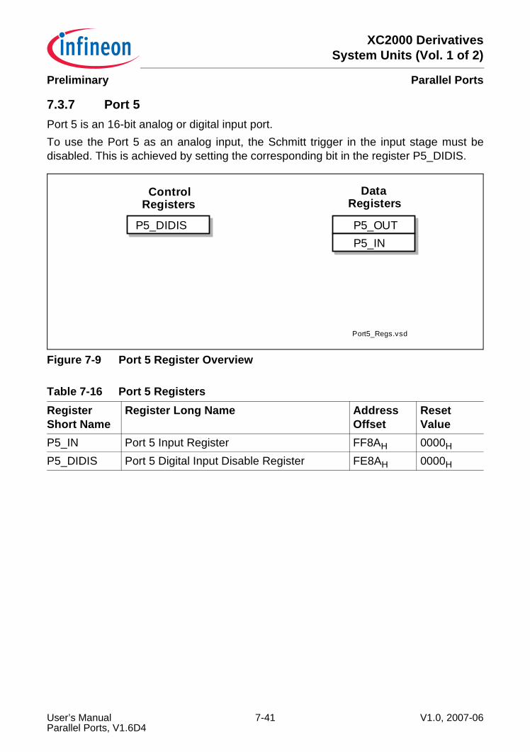
XC2000 DerivativesSystem Units (Vol. 1 of 2)
Parallel PortsPreliminary
7.3.7 Port 5Port 5 is an 16-bit analog or digital input port. To use the Port 5 as an analog input, the Schmitt trigger in the input stage must bedisabled. This is achieved by setting the corresponding bit in the register P5_DIDIS.
Figure 7-9 Port 5 Register Overview
Table 7-16 Port 5 RegistersRegister Short Name
Register Long Name Address Offset
Reset Value
P5_IN Port 5 Input Register FF8AH 0000H
P5_DIDIS Port 5 Digital Input Disable Register FE8AH 0000H
Port5_Regs.vsd
P5_DIDIS P5_OUT
DataRegisters
P5_IN
ControlRegisters
User’s Manual 7-41 V1.0, 2007-06Parallel Ports, V1.6D4

XC2000 DerivativesSystem Units (Vol. 1 of 2)
Parallel PortsPreliminary
7.3.7.1 Port 5 FunctionsThe following table describes the mapping between the pins of Port 5 and the related I/O signals.
Table 7-17 Port 5 Input/Output Functions
PortPin
I/O Select Connected Signal(s) From / to Module
P5.0 IP5.1 IP5.2 I TDI_A JTAGP5.3 I T3IN GPT12EP5.4 I T12HRB CCU63
T3EUD GPT12ETMS_A JTAG
P5.5 I T12HRB CCU60P5.6 IP5.7 IP5.8 I T12HRC CCU60
T13HRC CCU60T12HRC CCU61T13HRC CCU61T12HRC CCU62T13HRC CCU62T12HRC CCU63T13HRC CCU63
P5.9 I CC2_T7IN CAPCOM2P5.10 I BRKIN_A JTAGP5.11 IP5.12 IP5.13 I ERU_0B1 SCUP5.14 IP5.15 I ECTT3 CAN0 TTCAN
User’s Manual 7-42 V1.0, 2007-06Parallel Ports, V1.6D4

XC2000 DerivativesSystem Units (Vol. 1 of 2)
Parallel PortsPreliminary
7.3.8 Port 6Port 6 is an 4-bit GPIO port.
7.3.8.1 OverviewThe port registers of Port 6 are shown in Figure 7-10.For this port, all pins can be read as GPIO, from the Port Input Register.
Figure 7-10 Port 6 Register Overview
Table 7-18 Port 6 RegistersRegister Short Name
Register Long Name Address Offset
Reset Value
P6_OUT Port 6 Output Register FFAEH 0000H
P6_IN Port 6 Input Register FF8CH 0000H
P6_OMRL Port 6 Output Modification Register Low E9D8H 0000H
P6_POCON Port 6 Output Control Register E8ACH 0000H
P6_IOCR00 Port 6 Input/Output Control Register 0 E8C0H 0000H
P6_IOCR01 Port 6 Input/Output Control Register 1 E8C2H 0000H
P6_IOCR02 Port 6 Input/Output Control Register 2 E8C4H 0000H
P6_IOCR03 Port 6 Input/Output Control Register 4 E8C6H 0000H
P6_OMRL
Port6_Regs.vsd
P6_IOCR00 P6_OUT
ModificationRegisters
DataRegisters
P6_IN
ControlRegisters
P6_IOCR03:
P6_POCON
User’s Manual 7-43 V1.0, 2007-06Parallel Ports, V1.6D4
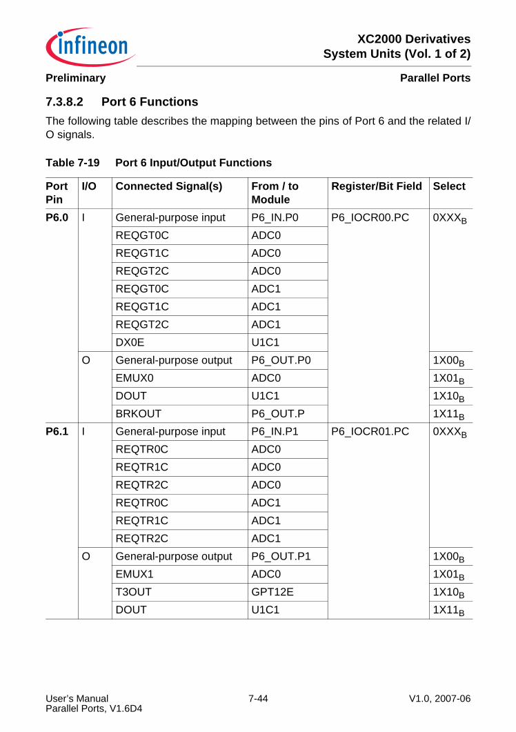
XC2000 DerivativesSystem Units (Vol. 1 of 2)
Parallel PortsPreliminary
7.3.8.2 Port 6 FunctionsThe following table describes the mapping between the pins of Port 6 and the related I/O signals.
Table 7-19 Port 6 Input/Output Functions
PortPin
I/O Connected Signal(s) From / to Module
Register/Bit Field Select
P6.0 I General-purpose input P6_IN.P0 P6_IOCR00.PC 0XXXB
REQGT0C ADC0REQGT1C ADC0REQGT2C ADC0REQGT0C ADC1REQGT1C ADC1REQGT2C ADC1DX0E U1C1
O General-purpose output P6_OUT.P0 1X00B
EMUX0 ADC0 1X01B
DOUT U1C1 1X10B
BRKOUT P6_OUT.P 1X11B
P6.1 I General-purpose input P6_IN.P1 P6_IOCR01.PC 0XXXB
REQTR0C ADC0REQTR1C ADC0REQTR2C ADC0REQTR0C ADC1REQTR1C ADC1REQTR2C ADC1
O General-purpose output P6_OUT.P1 1X00B
EMUX1 ADC0 1X01B
T3OUT GPT12E 1X10B
DOUT U1C1 1X11B
User’s Manual 7-44 V1.0, 2007-06Parallel Ports, V1.6D4
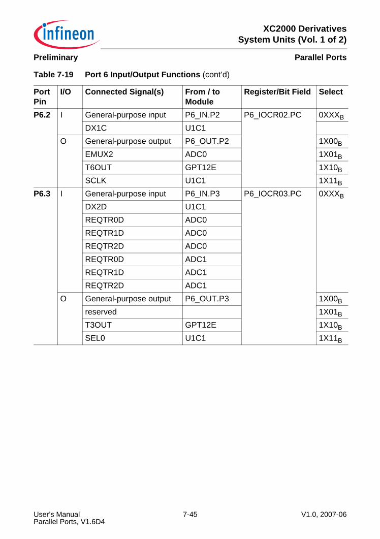
XC2000 DerivativesSystem Units (Vol. 1 of 2)
Parallel PortsPreliminary
P6.2 I General-purpose input P6_IN.P2 P6_IOCR02.PC 0XXXB
DX1C U1C1O General-purpose output P6_OUT.P2 1X00B
EMUX2 ADC0 1X01B
T6OUT GPT12E 1X10B
SCLK U1C1 1X11B
P6.3 I General-purpose input P6_IN.P3 P6_IOCR03.PC 0XXXB
DX2D U1C1REQTR0D ADC0REQTR1D ADC0REQTR2D ADC0REQTR0D ADC1REQTR1D ADC1REQTR2D ADC1
O General-purpose output P6_OUT.P3 1X00B
reserved 1X01B
T3OUT GPT12E 1X10B
SEL0 U1C1 1X11B
Table 7-19 Port 6 Input/Output Functions (cont’d)
PortPin
I/O Connected Signal(s) From / to Module
Register/Bit Field Select
User’s Manual 7-45 V1.0, 2007-06Parallel Ports, V1.6D4
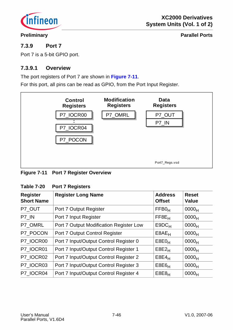
XC2000 DerivativesSystem Units (Vol. 1 of 2)
Parallel PortsPreliminary
7.3.9 Port 7Port 7 is a 5-bit GPIO port.
7.3.9.1 OverviewThe port registers of Port 7 are shown in Figure 7-11.For this port, all pins can be read as GPIO, from the Port Input Register.
Figure 7-11 Port 7 Register Overview
Table 7-20 Port 7 RegistersRegister Short Name
Register Long Name Address Offset
Reset Value
P7_OUT Port 7 Output Register FFB0H 0000H
P7_IN Port 7 Input Register FF8EH 0000H
P7_OMRL Port 7 Output Modification Register Low E9DCH 0000H
P7_POCON Port 7 Output Control Register E8AEH 0000H
P7_IOCR00 Port 7 Input/Output Control Register 0 E8E0H 0000H
P7_IOCR01 Port 7 Input/Output Control Register 1 E8E2H 0000H
P7_IOCR02 Port 7 Input/Output Control Register 2 E8E4H 0000H
P7_IOCR03 Port 7 Input/Output Control Register 3 E8E6H 0000H
P7_IOCR04 Port 7 Input/Output Control Register 4 E8E8H 0000H
P7_OMRL
Port7_Regs.vsd
P7_IOCR00 P7_OUT
ModificationRegisters
DataRegisters
P7_IN
ControlRegisters
P7_IOCR04:
P7_POCON
User’s Manual 7-46 V1.0, 2007-06Parallel Ports, V1.6D4
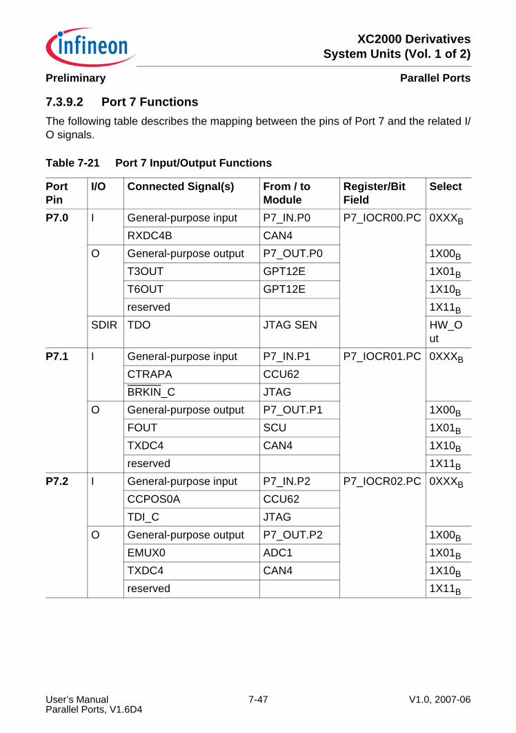
XC2000 DerivativesSystem Units (Vol. 1 of 2)
Parallel PortsPreliminary
7.3.9.2 Port 7 FunctionsThe following table describes the mapping between the pins of Port 7 and the related I/O signals.
Table 7-21 Port 7 Input/Output Functions
PortPin
I/O Connected Signal(s) From / to Module
Register/Bit Field
Select
P7.0 I General-purpose input P7_IN.P0 P7_IOCR00.PC 0XXXB
RXDC4B CAN4O General-purpose output P7_OUT.P0 1X00B
T3OUT GPT12E 1X01B
T6OUT GPT12E 1X10B
reserved 1X11B
SDIR TDO JTAG SEN HW_Out
P7.1 I General-purpose input P7_IN.P1 P7_IOCR01.PC 0XXXB
CTRAPA CCU62BRKIN_C JTAG
O General-purpose output P7_OUT.P1 1X00B
FOUT SCU 1X01B
TXDC4 CAN4 1X10B
reserved 1X11B
P7.2 I General-purpose input P7_IN.P2 P7_IOCR02.PC 0XXXB
CCPOS0A CCU62TDI_C JTAG
O General-purpose output P7_OUT.P2 1X00B
EMUX0 ADC1 1X01B
TXDC4 CAN4 1X10B
reserved 1X11B
User’s Manual 7-47 V1.0, 2007-06Parallel Ports, V1.6D4
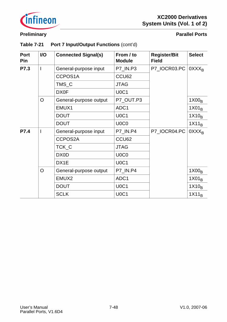
XC2000 DerivativesSystem Units (Vol. 1 of 2)
Parallel PortsPreliminary
P7.3 I General-purpose input P7_IN.P3 P7_IOCR03.PC 0XXXB
CCPOS1A CCU62TMS_C JTAGDX0F U0C1
O General-purpose output P7_OUT.P3 1X00B
EMUX1 ADC1 1X01B
DOUT U0C1 1X10B
DOUT U0C0 1X11B
P7.4 I General-purpose input P7_IN.P4 P7_IOCR04.PC 0XXXB
CCPOS2A CCU62TCK_C JTAGDX0D U0C0DX1E U0C1
O General-purpose output P7_IN.P4 1X00B
EMUX2 ADC1 1X01B
DOUT U0C1 1X10B
SCLK U0C1 1X11B
Table 7-21 Port 7 Input/Output Functions (cont’d)
PortPin
I/O Connected Signal(s) From / to Module
Register/Bit Field
Select
User’s Manual 7-48 V1.0, 2007-06Parallel Ports, V1.6D4

XC2000 DerivativesSystem Units (Vol. 1 of 2)
Parallel PortsPreliminary
7.3.10 Port 8Port 8 is an 7-bit GPIO port.
7.3.10.1 OverviewThe port registers of Port 8 are shown in Figure 7-12.For this port, all pins can be read as GPIO, from the Port Input Register.
Figure 7-12 Port 8 Register Overview
Table 7-22 Port 8 RegistersRegister Short Name
Register Long Name Address Offset
Reset Value
P8_OUT Port 8 Output Register FFB2H 0000H
P8_IN Port 8 Input Register FF90H 0000H
P8_OMRL Port 8 Output Modification Register Low E9E0H 0000H
P8_POCON Port 8 Output Control Register E8B0H 0000H
P8_IOCR00 Port 8 Input/Output Control Register 0 E900H 0000H
P8_IOCR01 Port 8 Input/Output Control Register 1 E902H 0000H
P8_IOCR02 Port 8 Input/Output Control Register 2 E904H 0000H
P8_IOCR03 Port 8 Input/Output Control Register 3 E906H 0000H
P8_IOCR04 Port 8 Input/Output Control Register 4 E908H 0000H
P8_IOCR05 Port 8 Input/Output Control Register 5 E90AH 0000H
P8_IOCR06 Port 8 Input/Output Control Register 6 E90CH 0000H
P8_OMRL
Port8_Regs.vsd
P8_IOCR00 P8_OUT
ModificationRegisters
DataRegisters
P8_IN
ControlRegisters
P8_IOCR06:
P8_POCON
User’s Manual 7-49 V1.0, 2007-06Parallel Ports, V1.6D4
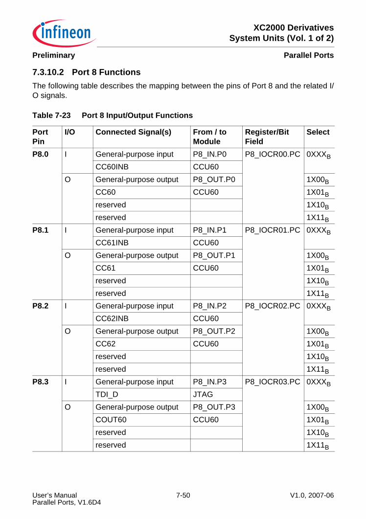
XC2000 DerivativesSystem Units (Vol. 1 of 2)
Parallel PortsPreliminary
7.3.10.2 Port 8 FunctionsThe following table describes the mapping between the pins of Port 8 and the related I/O signals.
Table 7-23 Port 8 Input/Output Functions
PortPin
I/O Connected Signal(s) From / to Module
Register/Bit Field
Select
P8.0 I General-purpose input P8_IN.P0 P8_IOCR00.PC 0XXXB
CC60INB CCU60O General-purpose output P8_OUT.P0 1X00B
CC60 CCU60 1X01B
reserved 1X10B
reserved 1X11B
P8.1 I General-purpose input P8_IN.P1 P8_IOCR01.PC 0XXXB
CC61INB CCU60O General-purpose output P8_OUT.P1 1X00B
CC61 CCU60 1X01B
reserved 1X10B
reserved 1X11B
P8.2 I General-purpose input P8_IN.P2 P8_IOCR02.PC 0XXXB
CC62INB CCU60O General-purpose output P8_OUT.P2 1X00B
CC62 CCU60 1X01B
reserved 1X10B
reserved 1X11B
P8.3 I General-purpose input P8_IN.P3 P8_IOCR03.PC 0XXXB
TDI_D JTAGO General-purpose output P8_OUT.P3 1X00B
COUT60 CCU60 1X01B
reserved 1X10B
reserved 1X11B
User’s Manual 7-50 V1.0, 2007-06Parallel Ports, V1.6D4
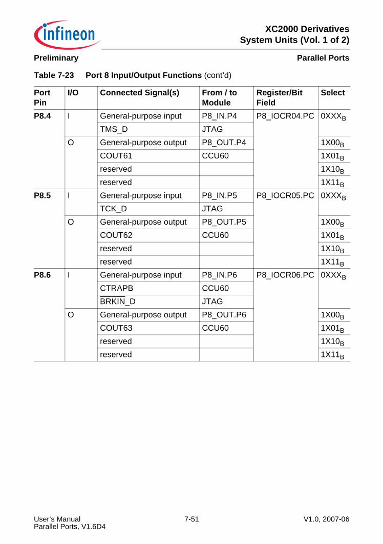
XC2000 DerivativesSystem Units (Vol. 1 of 2)
Parallel PortsPreliminary
P8.4 I General-purpose input P8_IN.P4 P8_IOCR04.PC 0XXXB
TMS_D JTAGO General-purpose output P8_OUT.P4 1X00B
COUT61 CCU60 1X01B
reserved 1X10B
reserved 1X11B
P8.5 I General-purpose input P8_IN.P5 P8_IOCR05.PC 0XXXB
TCK_D JTAGO General-purpose output P8_OUT.P5 1X00B
COUT62 CCU60 1X01B
reserved 1X10B
reserved 1X11B
P8.6 I General-purpose input P8_IN.P6 P8_IOCR06.PC 0XXXB
CTRAPB CCU60BRKIN_D JTAG
O General-purpose output P8_OUT.P6 1X00B
COUT63 CCU60 1X01B
reserved 1X10B
reserved 1X11B
Table 7-23 Port 8 Input/Output Functions (cont’d)
PortPin
I/O Connected Signal(s) From / to Module
Register/Bit Field
Select
User’s Manual 7-51 V1.0, 2007-06Parallel Ports, V1.6D4

XC2000 DerivativesSystem Units (Vol. 1 of 2)
Parallel PortsPreliminary
7.3.11 Port 9Port 9 is an 8-bit GPIO port.
7.3.11.1 OverviewThe port registers of Port 9 are shown in Figure 7-13.For this port, all pins can be read as GPIO, from the Port Input Register.
Figure 7-13 Port 9 Register Overview
Table 7-24 Port 9 RegistersRegister Short Name
Register Long Name Address Offset
Reset Value
P9_OUT Port 9 Output Register FFB4H 0000H
P9_IN Port 9 Input Register FF92H 0000H
P9_OMRL Port 9 Output Modification Register Low E9E4H 0000H
P9_POCON Port 9 Output Control Register E8B2H 0000H
P9_IOCR00 Port 9 Input/Output Control Register 0 E920H 0000H
P9_IOCR01 Port 9 Input/Output Control Register 1 E922H 0000H
P9_IOCR02 Port 9 Input/Output Control Register 2 E924H 0000H
P9_IOCR03 Port 9 Input/Output Control Register 3 E926H 0000H
P9_IOCR04 Port 9 Input/Output Control Register 4 E928H 0000H
P9_IOCR05 Port 9 Input/Output Control Register 5 E92AH 0000H
P9_IOCR06 Port 9 Input/Output Control Register 6 E92CH 0000H
P9_IOCR07 Port 9 Input/Output Control Register 7 E92EH 0000H
P9_OMRL
Port9_Regs.vsd
P9_IOCR00 P9_OUT
ModificationRegisters
DataRegisters
P9_IN
ControlRegisters
P9_IOCR07:
P9_POCON
User’s Manual 7-52 V1.0, 2007-06Parallel Ports, V1.6D4
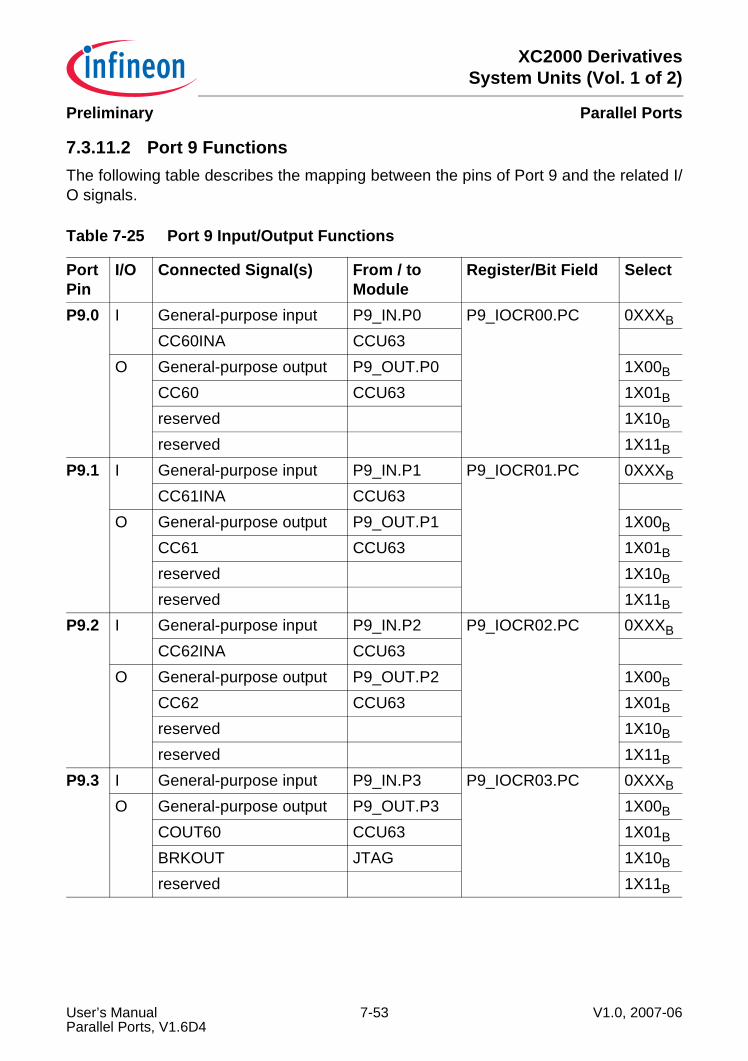
XC2000 DerivativesSystem Units (Vol. 1 of 2)
Parallel PortsPreliminary
7.3.11.2 Port 9 FunctionsThe following table describes the mapping between the pins of Port 9 and the related I/O signals.
Table 7-25 Port 9 Input/Output Functions
PortPin
I/O Connected Signal(s) From / to Module
Register/Bit Field Select
P9.0 I General-purpose input P9_IN.P0 P9_IOCR00.PC 0XXXB
CC60INA CCU63O General-purpose output P9_OUT.P0 1X00B
CC60 CCU63 1X01B
reserved 1X10B
reserved 1X11B
P9.1 I General-purpose input P9_IN.P1 P9_IOCR01.PC 0XXXB
CC61INA CCU63O General-purpose output P9_OUT.P1 1X00B
CC61 CCU63 1X01B
reserved 1X10B
reserved 1X11B
P9.2 I General-purpose input P9_IN.P2 P9_IOCR02.PC 0XXXB
CC62INA CCU63O General-purpose output P9_OUT.P2 1X00B
CC62 CCU63 1X01B
reserved 1X10B
reserved 1X11B
P9.3 I General-purpose input P9_IN.P3 P9_IOCR03.PC 0XXXB
O General-purpose output P9_OUT.P3 1X00B
COUT60 CCU63 1X01B
BRKOUT JTAG 1X10B
reserved 1X11B
User’s Manual 7-53 V1.0, 2007-06Parallel Ports, V1.6D4
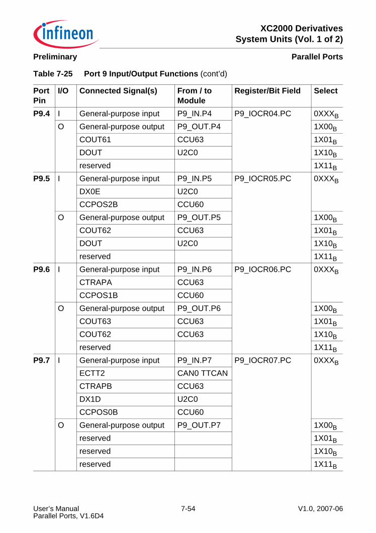
XC2000 DerivativesSystem Units (Vol. 1 of 2)
Parallel PortsPreliminary
P9.4 I General-purpose input P9_IN.P4 P9_IOCR04.PC 0XXXB
O General-purpose output P9_OUT.P4 1X00B
COUT61 CCU63 1X01B
DOUT U2C0 1X10B
reserved 1X11B
P9.5 I General-purpose input P9_IN.P5 P9_IOCR05.PC 0XXXB
DX0E U2C0CCPOS2B CCU60
O General-purpose output P9_OUT.P5 1X00B
COUT62 CCU63 1X01B
DOUT U2C0 1X10B
reserved 1X11B
P9.6 I General-purpose input P9_IN.P6 P9_IOCR06.PC 0XXXB
CTRAPA CCU63 CCPOS1B CCU60
O General-purpose output P9_OUT.P6 1X00B
COUT63 CCU63 1X01B
COUT62 CCU63 1X10B
reserved 1X11B
P9.7 I General-purpose input P9_IN.P7 P9_IOCR07.PC 0XXXB
ECTT2 CAN0 TTCANCTRAPB CCU63DX1D U2C0CCPOS0B CCU60
O General-purpose output P9_OUT.P7 1X00B
reserved 1X01B
reserved 1X10B
reserved 1X11B
Table 7-25 Port 9 Input/Output Functions (cont’d)
PortPin
I/O Connected Signal(s) From / to Module
Register/Bit Field Select
User’s Manual 7-54 V1.0, 2007-06Parallel Ports, V1.6D4
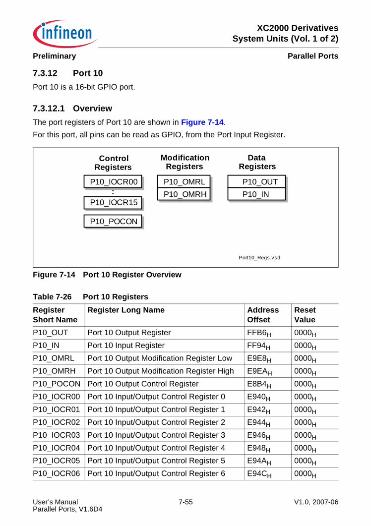
XC2000 DerivativesSystem Units (Vol. 1 of 2)
Parallel PortsPreliminary
7.3.12 Port 10Port 10 is a 16-bit GPIO port.
7.3.12.1 OverviewThe port registers of Port 10 are shown in Figure 7-14.For this port, all pins can be read as GPIO, from the Port Input Register.
Figure 7-14 Port 10 Register Overview
Table 7-26 Port 10 RegistersRegister Short Name
Register Long Name Address Offset
Reset Value
P10_OUT Port 10 Output Register FFB6H 0000H
P10_IN Port 10 Input Register FF94H 0000H
P10_OMRL Port 10 Output Modification Register Low E9E8H 0000H
P10_OMRH Port 10 Output Modification Register High E9EAH 0000H
P10_POCON Port 10 Output Control Register E8B4H 0000H
P10_IOCR00 Port 10 Input/Output Control Register 0 E940H 0000H
P10_IOCR01 Port 10 Input/Output Control Register 1 E942H 0000H
P10_IOCR02 Port 10 Input/Output Control Register 2 E944H 0000H
P10_IOCR03 Port 10 Input/Output Control Register 3 E946H 0000H
P10_IOCR04 Port 10 Input/Output Control Register 4 E948H 0000H
P10_IOCR05 Port 10 Input/Output Control Register 5 E94AH 0000H
P10_IOCR06 Port 10 Input/Output Control Register 6 E94CH 0000H
P10_OMRL
Port10_Regs.vsd
P10_IOCR00 P10_OUT
ModificationRegisters
DataRegisters
P10_IN
ControlRegisters
P10_IOCR15:
P10_POCON
P10_OMRH
User’s Manual 7-55 V1.0, 2007-06Parallel Ports, V1.6D4
XC2000 DerivativesSystem Units (Vol. 1 of 2)
Parallel PortsPreliminary
7.3.12.2 Port 10 FunctionsThe following table describes the mapping between the pins of Port 10 and the relatedI/O signals.
P10_IOCR07 Port 10 Input/Output Control Register 7 E94EH 0000H
P10_IOCR08 Port 10 Input/Output Control Register 8 E950H 0000H
P10_IOCR09 Port 10 Input/Output Control Register 9 E952H 0000H
P10_IOCR10 Port 10 Input/Output Control Register 10 E954H 0000H
P10_IOCR11 Port 10 Input/Output Control Register 11 E956H 0000H
P10_IOCR12 Port 10 Input/Output Control Register 12 E958H 0000H
P10_IOCR13 Port 10 Input/Output Control Register 13 E95AH 0000H
P10_IOCR14 Port 10 Input/Output Control Register 14 E95CH 0000H
P10_IOCR15 Port 10 Input/Output Control Register 15 E95EH 0000H
Table 7-27 Port 10 Input/Output Functions
PortPin
I/O Connected Signal(s) From / to Module
Register/Bit Field
Select
P10.0 I General-purpose input P10_IN.P0 P10_IOCR00.PC 0XXXB
D0 EBCCC60INA CCU60DX0A U0C0DX0A U0C1
O General-purpose output P10_OUT.P0 1X00B
DOUT U0C1 1X01B
CC60 CCU60 1X10B
reserved 1X11B
DIR1 AD0 EBC; EN1 HW_Out
Table 7-26 Port 10 Registers (cont’d)
Register Short Name
Register Long Name Address Offset
Reset Value
User’s Manual 7-56 V1.0, 2007-06Parallel Ports, V1.6D4
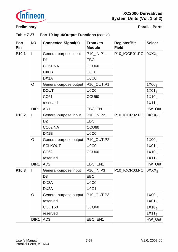
XC2000 DerivativesSystem Units (Vol. 1 of 2)
Parallel PortsPreliminary
P10.1 I General-purpose input P10_IN.P1 P10_IOCR01.PC 0XXXB
D1 EBCCC61INA CCU60DX0B U0C0DX1A U0C0
O General-purpose output P10_OUT.P1 1X00B
DOUT U0C0 1X01B
CC61 CCU60 1X10B
reserved 1X11B
DIR1 AD1 EBC; EN1 HW_OutP10.2 I General-purpose input P10_IN.P2 P10_IOCR02.PC 0XXXB
D2 EBCCC62INA CCU60DX1B U0C0
O General-purpose output P10_OUT.P2 1X00B
SCLKOUT U0C0 1X01B
CC62 CCU60 1X10B
reserved 1X11B
DIR1 AD2 EBC; EN1 HW_OutP10.3 I General-purpose input P10_IN.P3 P10_IOCR03.PC 0XXXB
D3 EBCDX2A U0C0DX2A U0C1
O General-purpose output P10_OUT.P3 1X00B
reserved 1X01B
COUT60 CCU60 1X10B
reserved 1X11B
DIR1 AD3 EBC; EN1 HW_Out
Table 7-27 Port 10 Input/Output Functions (cont’d)
PortPin
I/O Connected Signal(s) From / to Module
Register/Bit Field
Select
User’s Manual 7-57 V1.0, 2007-06Parallel Ports, V1.6D4
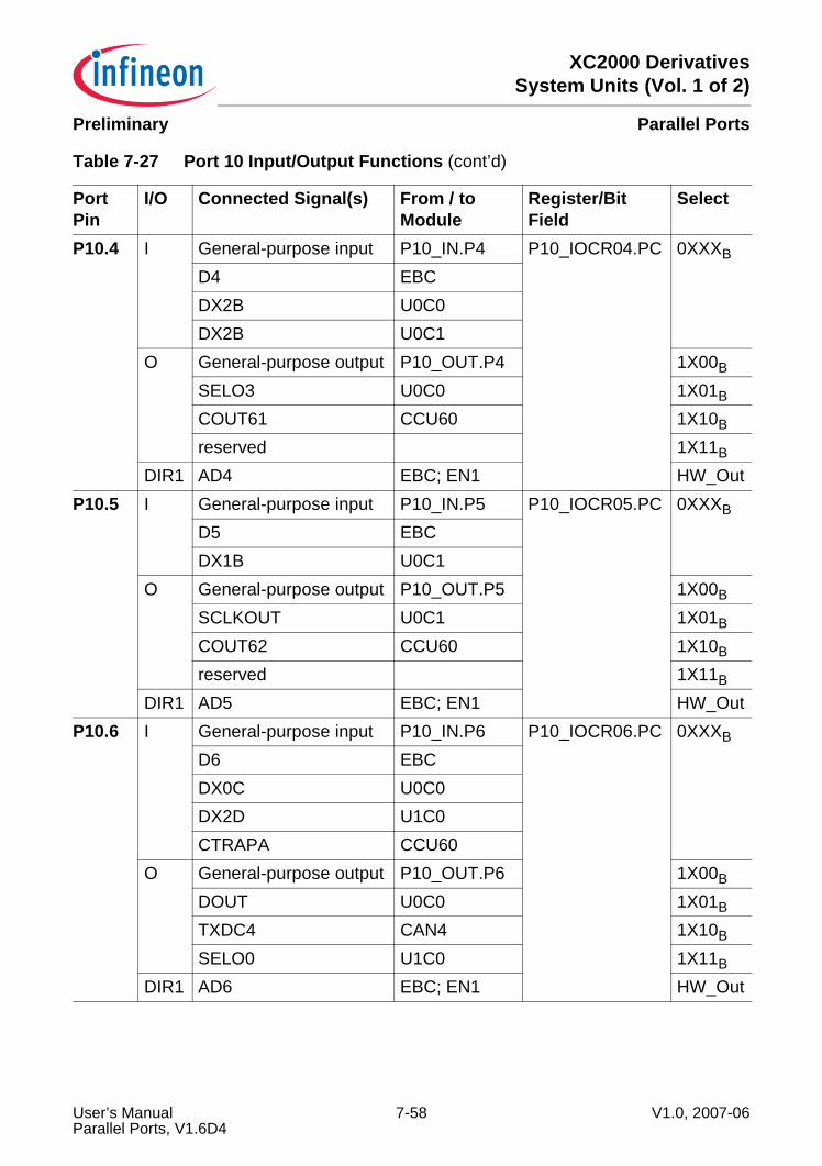
XC2000 DerivativesSystem Units (Vol. 1 of 2)
Parallel PortsPreliminary
P10.4 I General-purpose input P10_IN.P4 P10_IOCR04.PC 0XXXB
D4 EBCDX2B U0C0DX2B U0C1
O General-purpose output P10_OUT.P4 1X00B
SELO3 U0C0 1X01B
COUT61 CCU60 1X10B
reserved 1X11B
DIR1 AD4 EBC; EN1 HW_OutP10.5 I General-purpose input P10_IN.P5 P10_IOCR05.PC 0XXXB
D5 EBCDX1B U0C1
O General-purpose output P10_OUT.P5 1X00B
SCLKOUT U0C1 1X01B
COUT62 CCU60 1X10B
reserved 1X11B
DIR1 AD5 EBC; EN1 HW_OutP10.6 I General-purpose input P10_IN.P6 P10_IOCR06.PC 0XXXB
D6 EBCDX0C U0C0DX2D U1C0CTRAPA CCU60
O General-purpose output P10_OUT.P6 1X00B
DOUT U0C0 1X01B
TXDC4 CAN4 1X10B
SELO0 U1C0 1X11B
DIR1 AD6 EBC; EN1 HW_Out
Table 7-27 Port 10 Input/Output Functions (cont’d)
PortPin
I/O Connected Signal(s) From / to Module
Register/Bit Field
Select
User’s Manual 7-58 V1.0, 2007-06Parallel Ports, V1.6D4
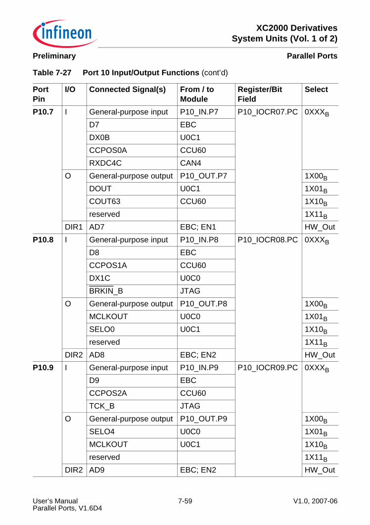
XC2000 DerivativesSystem Units (Vol. 1 of 2)
Parallel PortsPreliminary
P10.7 I General-purpose input P10_IN.P7 P10_IOCR07.PC 0XXXB
D7 EBCDX0B U0C1CCPOS0A CCU60RXDC4C CAN4
O General-purpose output P10_OUT.P7 1X00B
DOUT U0C1 1X01B
COUT63 CCU60 1X10B
reserved 1X11B
DIR1 AD7 EBC; EN1 HW_OutP10.8 I General-purpose input P10_IN.P8 P10_IOCR08.PC 0XXXB
D8 EBCCCPOS1A CCU60DX1C U0C0BRKIN_B JTAG
O General-purpose output P10_OUT.P8 1X00B
MCLKOUT U0C0 1X01B
SELO0 U0C1 1X10B
reserved 1X11B
DIR2 AD8 EBC; EN2 HW_OutP10.9 I General-purpose input P10_IN.P9 P10_IOCR09.PC 0XXXB
D9 EBCCCPOS2A CCU60TCK_B JTAG
O General-purpose output P10_OUT.P9 1X00B
SELO4 U0C0 1X01B
MCLKOUT U0C1 1X10B
reserved 1X11B
DIR2 AD9 EBC; EN2 HW_Out
Table 7-27 Port 10 Input/Output Functions (cont’d)
PortPin
I/O Connected Signal(s) From / to Module
Register/Bit Field
Select
User’s Manual 7-59 V1.0, 2007-06Parallel Ports, V1.6D4
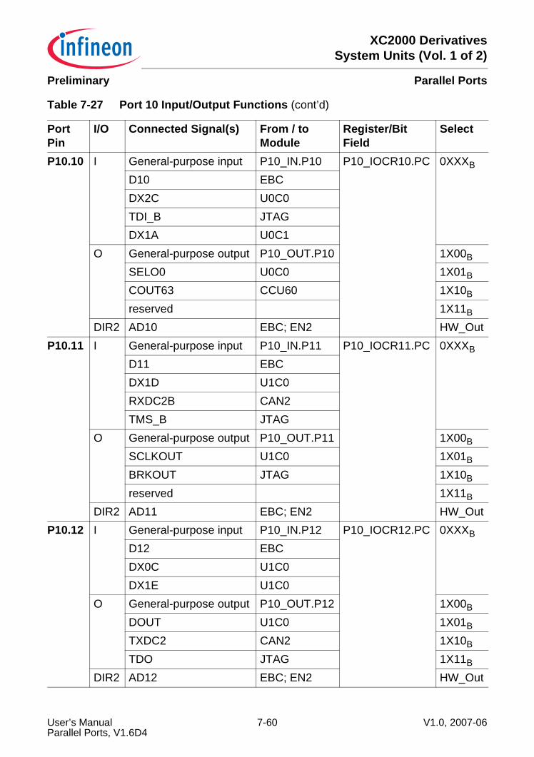
XC2000 DerivativesSystem Units (Vol. 1 of 2)
Parallel PortsPreliminary
P10.10 I General-purpose input P10_IN.P10 P10_IOCR10.PC 0XXXB
D10 EBCDX2C U0C0TDI_B JTAGDX1A U0C1
O General-purpose output P10_OUT.P10 1X00B
SELO0 U0C0 1X01B
COUT63 CCU60 1X10B
reserved 1X11B
DIR2 AD10 EBC; EN2 HW_OutP10.11 I General-purpose input P10_IN.P11 P10_IOCR11.PC 0XXXB
D11 EBCDX1D U1C0RXDC2B CAN2TMS_B JTAG
O General-purpose output P10_OUT.P11 1X00B
SCLKOUT U1C0 1X01B
BRKOUT JTAG 1X10B
reserved 1X11B
DIR2 AD11 EBC; EN2 HW_OutP10.12 I General-purpose input P10_IN.P12 P10_IOCR12.PC 0XXXB
D12 EBCDX0C U1C0DX1E U1C0
O General-purpose output P10_OUT.P12 1X00B
DOUT U1C0 1X01B
TXDC2 CAN2 1X10B
TDO JTAG 1X11B
DIR2 AD12 EBC; EN2 HW_Out
Table 7-27 Port 10 Input/Output Functions (cont’d)
PortPin
I/O Connected Signal(s) From / to Module
Register/Bit Field
Select
User’s Manual 7-60 V1.0, 2007-06Parallel Ports, V1.6D4
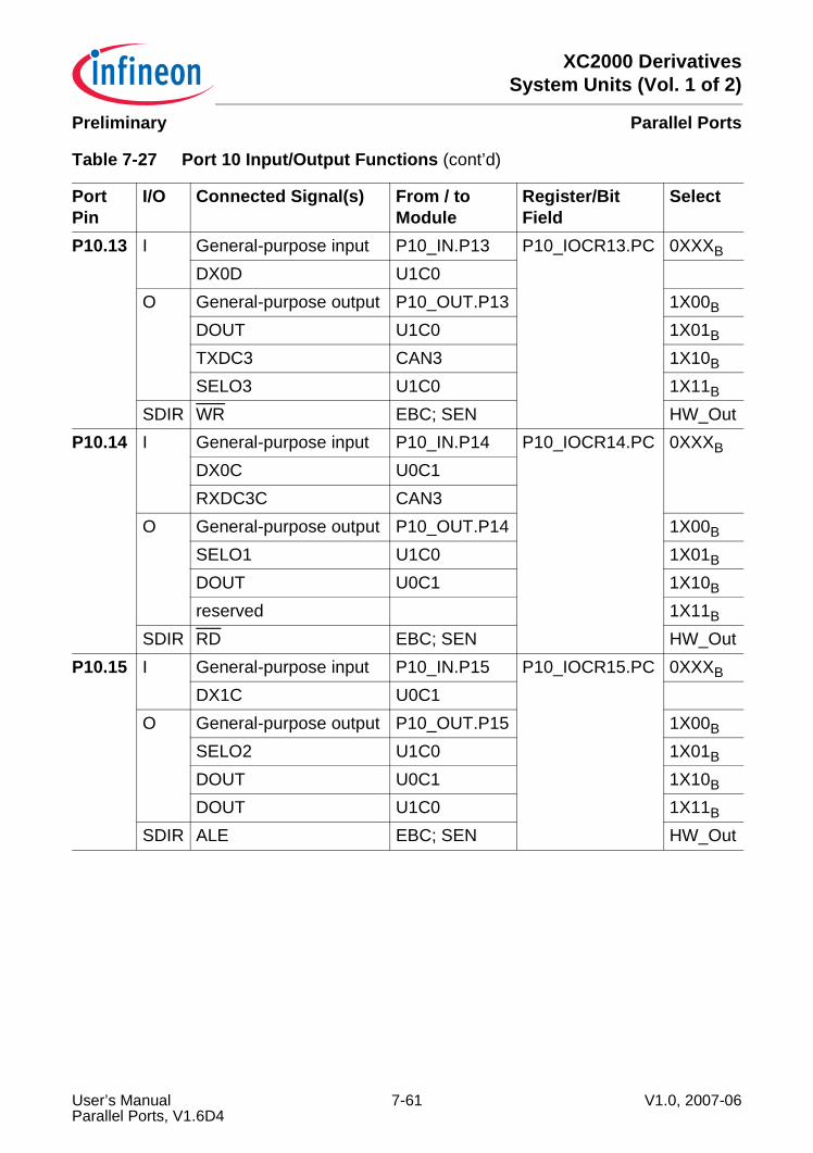
XC2000 DerivativesSystem Units (Vol. 1 of 2)
Parallel PortsPreliminary
P10.13 I General-purpose input P10_IN.P13 P10_IOCR13.PC 0XXXB
DX0D U1C0O General-purpose output P10_OUT.P13 1X00B
DOUT U1C0 1X01B
TXDC3 CAN3 1X10B
SELO3 U1C0 1X11B
SDIR WR EBC; SEN HW_OutP10.14 I General-purpose input P10_IN.P14 P10_IOCR14.PC 0XXXB
DX0C U0C1RXDC3C CAN3
O General-purpose output P10_OUT.P14 1X00B
SELO1 U1C0 1X01B
DOUT U0C1 1X10B
reserved 1X11B
SDIR RD EBC; SEN HW_OutP10.15 I General-purpose input P10_IN.P15 P10_IOCR15.PC 0XXXB
DX1C U0C1O General-purpose output P10_OUT.P15 1X00B
SELO2 U1C0 1X01B
DOUT U0C1 1X10B
DOUT U1C0 1X11B
SDIR ALE EBC; SEN HW_Out
Table 7-27 Port 10 Input/Output Functions (cont’d)
PortPin
I/O Connected Signal(s) From / to Module
Register/Bit Field
Select
User’s Manual 7-61 V1.0, 2007-06Parallel Ports, V1.6D4
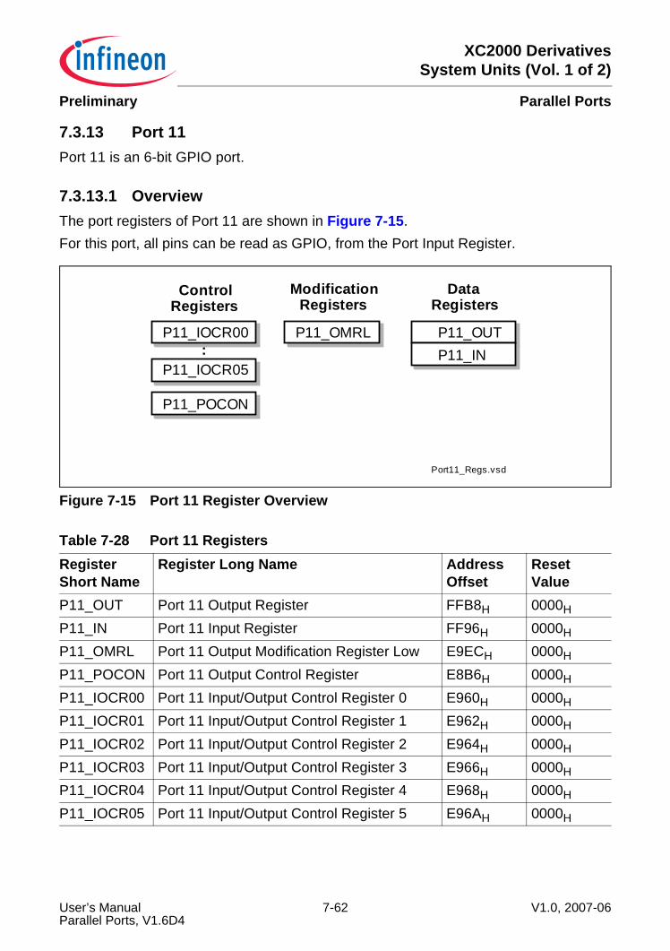
XC2000 DerivativesSystem Units (Vol. 1 of 2)
Parallel PortsPreliminary
7.3.13 Port 11Port 11 is an 6-bit GPIO port.
7.3.13.1 OverviewThe port registers of Port 11 are shown in Figure 7-15.For this port, all pins can be read as GPIO, from the Port Input Register.
Figure 7-15 Port 11 Register Overview
Table 7-28 Port 11 RegistersRegister Short Name
Register Long Name Address Offset
Reset Value
P11_OUT Port 11 Output Register FFB8H 0000H
P11_IN Port 11 Input Register FF96H 0000H
P11_OMRL Port 11 Output Modification Register Low E9ECH 0000H
P11_POCON Port 11 Output Control Register E8B6H 0000H
P11_IOCR00 Port 11 Input/Output Control Register 0 E960H 0000H
P11_IOCR01 Port 11 Input/Output Control Register 1 E962H 0000H
P11_IOCR02 Port 11 Input/Output Control Register 2 E964H 0000H
P11_IOCR03 Port 11 Input/Output Control Register 3 E966H 0000H
P11_IOCR04 Port 11 Input/Output Control Register 4 E968H 0000H
P11_IOCR05 Port 11 Input/Output Control Register 5 E96AH 0000H
P11_OMRL
Port11_Regs.vsd
P11_IOCR00 P11_OUT
ModificationRegisters
DataRegisters
P11_IN
ControlRegisters
P11_IOCR05:
P11_POCON
User’s Manual 7-62 V1.0, 2007-06Parallel Ports, V1.6D4
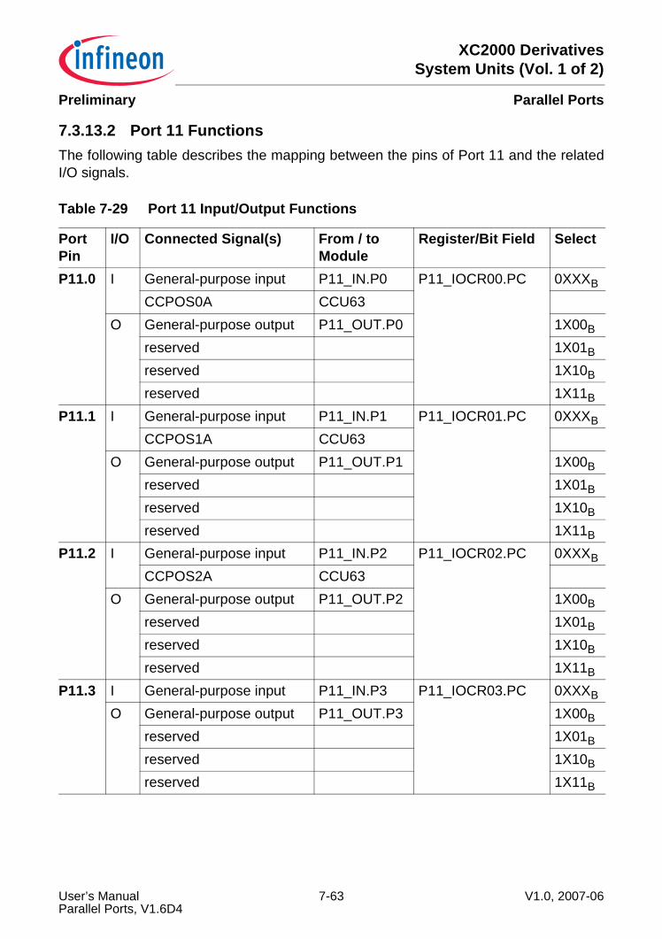
XC2000 DerivativesSystem Units (Vol. 1 of 2)
Parallel PortsPreliminary
7.3.13.2 Port 11 FunctionsThe following table describes the mapping between the pins of Port 11 and the relatedI/O signals.
Table 7-29 Port 11 Input/Output Functions
PortPin
I/O Connected Signal(s) From / to Module
Register/Bit Field Select
P11.0 I General-purpose input P11_IN.P0 P11_IOCR00.PC 0XXXB
CCPOS0A CCU63O General-purpose output P11_OUT.P0 1X00B
reserved 1X01B
reserved 1X10B
reserved 1X11B
P11.1 I General-purpose input P11_IN.P1 P11_IOCR01.PC 0XXXB
CCPOS1A CCU63O General-purpose output P11_OUT.P1 1X00B
reserved 1X01B
reserved 1X10B
reserved 1X11B
P11.2 I General-purpose input P11_IN.P2 P11_IOCR02.PC 0XXXB
CCPOS2A CCU63O General-purpose output P11_OUT.P2 1X00B
reserved 1X01B
reserved 1X10B
reserved 1X11B
P11.3 I General-purpose input P11_IN.P3 P11_IOCR03.PC 0XXXB
O General-purpose output P11_OUT.P3 1X00B
reserved 1X01B
reserved 1X10B
reserved 1X11B
User’s Manual 7-63 V1.0, 2007-06Parallel Ports, V1.6D4
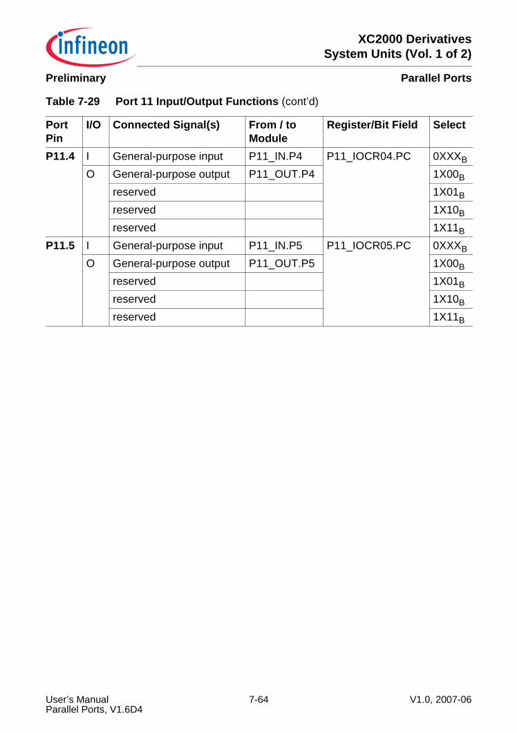
XC2000 DerivativesSystem Units (Vol. 1 of 2)
Parallel PortsPreliminary
P11.4 I General-purpose input P11_IN.P4 P11_IOCR04.PC 0XXXB
O General-purpose output P11_OUT.P4 1X00B
reserved 1X01B
reserved 1X10B
reserved 1X11B
P11.5 I General-purpose input P11_IN.P5 P11_IOCR05.PC 0XXXB
O General-purpose output P11_OUT.P5 1X00B
reserved 1X01B
reserved 1X10B
reserved 1X11B
Table 7-29 Port 11 Input/Output Functions (cont’d)
PortPin
I/O Connected Signal(s) From / to Module
Register/Bit Field Select
User’s Manual 7-64 V1.0, 2007-06Parallel Ports, V1.6D4
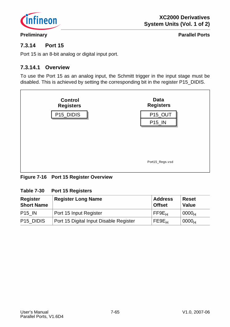
XC2000 DerivativesSystem Units (Vol. 1 of 2)
Parallel PortsPreliminary
7.3.14 Port 15Port 15 is an 8-bit analog or digital input port.
7.3.14.1 OverviewTo use the Port 15 as an analog input, the Schmitt trigger in the input stage must bedisabled. This is achieved by setting the corresponding bit in the register P15_DIDIS.
Figure 7-16 Port 15 Register Overview
Table 7-30 Port 15 RegistersRegister Short Name
Register Long Name Address Offset
Reset Value
P15_IN Port 15 Input Register FF9EH 0000H
P15_DIDIS Port 15 Digital Input Disable Register FE9EH 0000H
Port15_Regs.vsd
P15_DIDIS P15_OUT
DataRegisters
P15_IN
ControlRegisters
User’s Manual 7-65 V1.0, 2007-06Parallel Ports, V1.6D4
XC2000 DerivativesSystem Units (Vol. 1 of 2)
Parallel PortsPreliminary
7.3.14.2 Port 15 FunctionsThe following table describes the mapping between the pins of Port 15 and the relatedI/O signals.
Table 7-31 Port 15 Input/Output Functions
PortPin
I/O Select Connected Signal(s) From / to Module
P15.0 IP15.1 IP15.2 I T5IN GPT12EP15.3 I T5EUD GPT12EP15.4 I T6IN GPT12EP15.5 I T6EUD GPT12EP15.6 IP15.7 I
User’s Manual 7-66 V1.0, 2007-06Parallel Ports, V1.6D4
XC2000 DerivativesSystem Units (Vol. 1 of 2)
Dedicated PinsPreliminary
8 Dedicated PinsMost of the input/output or control signals of the functional the XC2000 are realized asalternate functions of pins of the parallel ports. There is, however, a number of signalsthat use separate pins, including the oscillator, special control signals and, of course, thepower supply.Table 8-1 summarizes the dedicated pins of the XC2000.
The Power-On Reset Input PORST allows to put the XC2000 into the well defined resetcondition either at power-up or external events like a hardware failure or manual reset.The External Service Request Inputs ESR0, ESR1, and ESR2 can be used for severalsystem-related functions:• trigger interrupt or trap (Class A or Class B) requests via an external signal (e.g. a
power-fail signal)• generate wake-up request signals• generate hardware reset requests (ESR0 is bidirectional by default, ESR1 and ESR2
can optionally output a reset signal)• data/control input for CCU6x, MultiCAN, and USIC (ESR1 or ESR2)• software-controlled input/output signal
Table 8-1 XC2000 Dedicated PinsPin(s) FunctionPORST Power-On Reset InputESR0 External Service Request Input 0ESR1 External Service Request Input 1ESR2 External Service Request Input 2XTAL1, XTAL2 Oscillator Input/Output (main oscillator)TESTM Test Mode EnableTRST Test-System Reset InputTRef Control Pin for Core Voltage GenerationVAREFx, VAGND Power Supply for the Analog/Digital Converter(s)VDDIM Digital Core Supply for Domain M (1 pin)VDDI1 Digital Core Supply for Domain 1 (3 pins)VDDPA Digital Pad Supply for Domain A (1 pin)VDDPB Digital Pad Supply for Domain B (8 pins)VSS Digital Ground (4 pins)
User’s Manual 8-1 V1.0, 2007-06DediPins_X7, V2.0
XC2000 DerivativesSystem Units (Vol. 1 of 2)
Dedicated PinsPreliminary
The Oscillator Input XTAL1 and Output XTAL2 connect the internal Main Oscillatorto the external crystal. The oscillator provides an inverter and a feedback element. Thestandard external oscillator circuitry (see Section 6.1.2) comprises the crystal, two lowend capacitors and series resistor to limit the current through the crystal. The mainoscillator is intended for the generation of a high-precision operating clock signal for theXC2000.An external clock signal may be fed to the input XTAL1, leaving XTAL2 open. The currentlogic state of input XTAL1 can be read via a status flag, so XTAL1 can be used as digitalinput if neither the oscillator interface nor the clock input is required.Note: Pin XTAL1 belongs to the core power domain DMP_M. All input signals, therefore,
must be within the core voltage range.
The Test Mode Input TESTM puts the XC2000 into a test mode, which is used duringthe production tests of the device. In test mode, the XC2000 behaves different fromnormal operation. Therefore, pin TESTM must be held HIGH (connect to VDDPB) fornormal operation in an application system.The Test Reset Input TRST puts the XC2000’s debug system into reset state. Duringnormal operation this input should be held low. For debugging purposes the on-chipdebugging system can be enabled by driving pin TRST high at the rising edge of PORST.The Control Pin for Core Voltage Generation TRef selects the generation method forthe core supply voltage VDDI. Connect TRef to VDDPB to use the on-chip EVRs, connectTRef to VDDI1 for external core voltage supply (on-chip EVRs off).The Analog Reference Voltage Supply pins VAREFx and VAGND provide separatereference voltage for the on-chip Analog/Digital-Converter(s). This reduces the noisethat is coupled to the analog input signals from the digital logic sections and so improvesthe stability of the conversion results, when VAREF and VAGND are properly discoupledfrom VDD and VSS. Also, because conversion results are generated in relation to thereference voltages, ratiometric conversions are easily achieved.Note: Channel 0 of each module can be used as an alternate reference voltage input.
The Core Supply pins VDDIM/VDDI1 serve two purposes: While the on-chip EVVRsprovide the power for the core logic of the XC2000 these pins connect the EVVRs to theirexternal buffer capacitors. For external supply, the core voltage is applied to these pins.The respective VDDI/VSS pairs should be decoupled as close to the pins as possible. Useceramic capacitors and observe their values recommended in the respective DataSheet.The Power Supply pins VDDPA/VDDPB provide the power supply for all the digital logic ofthe XC2000. Each power domain (DMP_A and DMP_B) can be supplied with anarbitrary voltage within the specified supply voltage range (please refer to thecorresponding Data Sheets). These pins supply the output drivers as well as the on-chipEVVRs, except for external core voltage supply. The respective VDDP/VSS pairs shouldbe decoupled as close to the pins as possible.
User’s Manual 8-2 V1.0, 2007-06DediPins_X7, V2.0
XC2000 DerivativesSystem Units (Vol. 1 of 2)
Dedicated PinsPreliminary
The Ground Reference pins VSS provide the ground reference voltage for the powersupplies as well as the reference voltage for the input signals.Note: All VDDx pins and all VSS pins must be connected to the power supplies and
ground, respectively.
User’s Manual 8-3 V1.0, 2007-06DediPins_X7, V2.0
XC2000 DerivativesSystem Units (Vol. 1 of 2)
Dedicated PinsPreliminary
User’s Manual 8-4 V1.0, 2007-06DediPins_X7, V2.0
XC2000 DerivativesSystem Units (Vol. 1 of 2)
The External Bus Controller EBCPreliminary
9 The External Bus Controller EBC All external memory accesses are performed by a particular on-chip External BusController (EBC). It can be programmed either to Single Chip Mode when no externalmemory is required at all, or dynamically (depending on the selected address range,belonging to a chip-select signal) to one of four different external memory access modes,which are as follows:• 16/17/18/19 … 24-bit Addresses, 16-bit Data, Demultiplexed• 16/17/18/19 … 24-bit Addresses, 16-bit Data, Multiplexed• 16/17/18/19 … 24-bit Addresses, 8-bit Data, Multiplexed• 16/17/18/19 … 24-bit Addresses, 8-bit Data, DemultiplexedNote: The following description refers to the general EBC feature set. In packages
smaller than 144-pin, some features are not available, see Table 9-1.
In the multiplexed bus modes intra-segment address outputs and data input/outputs areoverlaid on 16 port pins. High order address (segment) lines are mapped to separateport pins. In the demultiplexed bus modes, address outputs and data input/outputs arenot overlaid but mapped to the port pins separately. For applications which do not useall address lines for external devices, the external address space can be restricted to8 Mbytes, 4 Mbytes, 2 Mbytes, 1 Mbyte, 512 Kbytes, 256 Kbytes, 128 Kbytes or64 Kbytes. In this case seven, six, five and so on, or no segment address lines are active.Up to 5 external CS signals can be generated in order to save external glue logic. Accessto very slow memories is supported via a particular ‘Ready’ function. A HOLD/HLDAprotocol is available for bus arbitration.The XC2000 External Bus Controller (EBC) allows access to externalperipherals/memories and to internal LXBus modules. The LXBus is an internalrepresentation of the ExtBus and it controls accesses to integrated peripherals andmodules in the same way as accesses to external components. Because some ExtBuscontrol signals are generally configurable, related additional control signals arenecessary for the internal LXBus to support its maybe different configuration.The function of the EBC is controlled via a set of configuration registers. The basic andgeneral behaviour is programmed via the mode-selection registers EBCMOD0 andEBCMOD1.Additionally to the supported external bus chip-select channels, one LXBus chip selectchannel is provided (both types together handled as ‘external’ chip select channels).With one exception, each of these chip-select signals is programmable via a set ofregisters. The Function CONtrol register for CSx (FCONCSx) register specifies theexternal bus/LXBus cycles in terms of address (multiplexed/demultiplexed), data(16-bit/8-bit), READY control, and chip-select enable. The timing of the bus access iscontrolled by the Timing CONfiguration registers for CSx (TCONCSx), which specify thetiming of the bus cycle with the lengths of the different access phases. All these
User’s Manual 9-1 V1.0, 2007-06EBC_X8, V1.0d1
XC2000 DerivativesSystem Units (Vol. 1 of 2)
The External Bus Controller EBCPreliminary
parameters are used for accesses within a specific address area that is defined via thecorresponding ADDRess SELect register ADDRSELx.The five register sets (FCONCSx/TCONCSx/ADDRSELx) define five independent andprogrammable “address windows”, whereas all external accesses outside thesewindows are controlled via registers FCONCS0 and TCONCS0. Chip Select signals CS0… CS4 belong to accesses on external bus, the additional Chip Select CS7 is used foraccess to the internal MultiCAN and USIC module on LXBus.The external bus timing is related to the reference CLocK OUTput (CLKOUT). All bussignals are generated in relation to the rising edge of this clock. The external bus protocolis compatible with those of the standard C166 Family. However, the external bus timingis improved in terms of wait-state granularity and signal flexibility.These improvements are configured via an enhanced register set (see above) incomparison to C166 Family. The C16x registers SYSCON and BUSCONx are no longerused. But because the configuration of the external bus controller is done during theapplication initialization, only some initialization code has to be adapted for using thenew EBC module instead of the C16x external bus controller.
User’s Manual 9-2 V1.0, 2007-06EBC_X8, V1.0d1
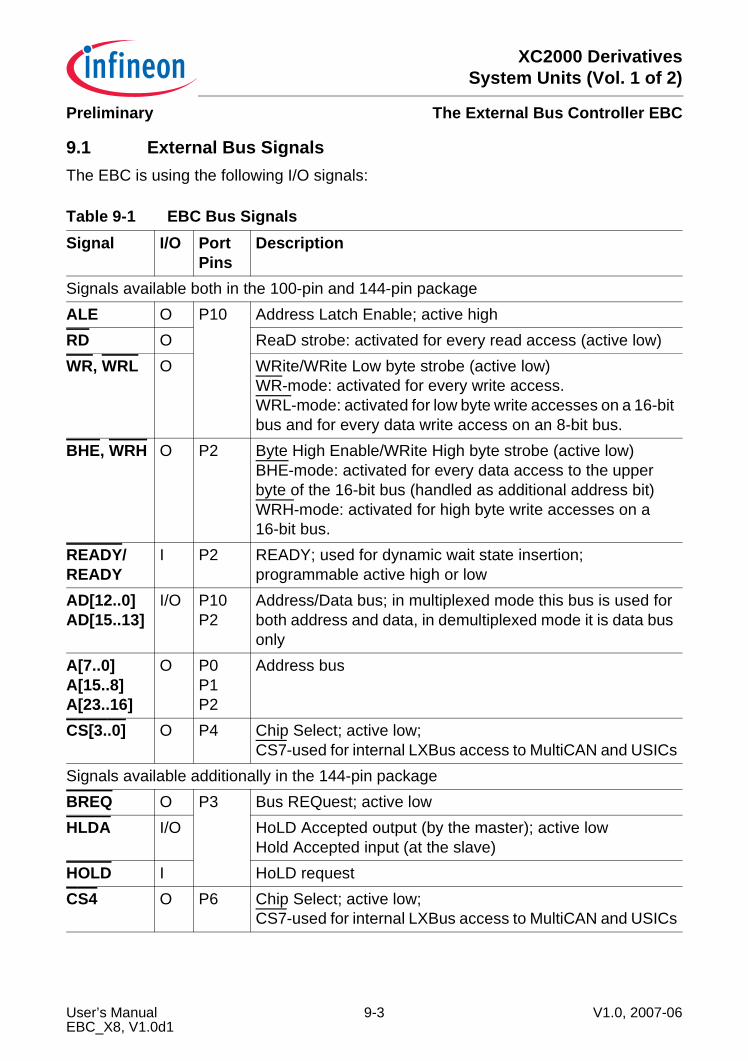
XC2000 DerivativesSystem Units (Vol. 1 of 2)
The External Bus Controller EBCPreliminary
9.1 External Bus SignalsThe EBC is using the following I/O signals:
Table 9-1 EBC Bus SignalsSignal I/O Port
PinsDescription
Signals available both in the 100-pin and 144-pin packageALE O P10 Address Latch Enable; active highRD O ReaD strobe: activated for every read access (active low)WR, WRL O WRite/WRite Low byte strobe (active low)
WR-mode: activated for every write access.WRL-mode: activated for low byte write accesses on a 16-bit bus and for every data write access on an 8-bit bus.
BHE, WRH O P2 Byte High Enable/WRite High byte strobe (active low)BHE-mode: activated for every data access to the upper byte of the 16-bit bus (handled as additional address bit)WRH-mode: activated for high byte write accesses on a 16-bit bus.
READY/READY
I P2 READY; used for dynamic wait state insertion; programmable active high or low
AD[12..0]AD[15..13]
I/O P10P2
Address/Data bus; in multiplexed mode this bus is used for both address and data, in demultiplexed mode it is data bus only
A[7..0]A[15..8]A[23..16]
O P0P1P2
Address bus
CS[3..0] O P4 Chip Select; active low;CS7-used for internal LXBus access to MultiCAN and USICs
Signals available additionally in the 144-pin packageBREQ O P3 Bus REQuest; active lowHLDA I/O HoLD Accepted output (by the master); active low
Hold Accepted input (at the slave)HOLD I HoLD requestCS4 O P6 Chip Select; active low;
CS7-used for internal LXBus access to MultiCAN and USICs
User’s Manual 9-3 V1.0, 2007-06EBC_X8, V1.0d1
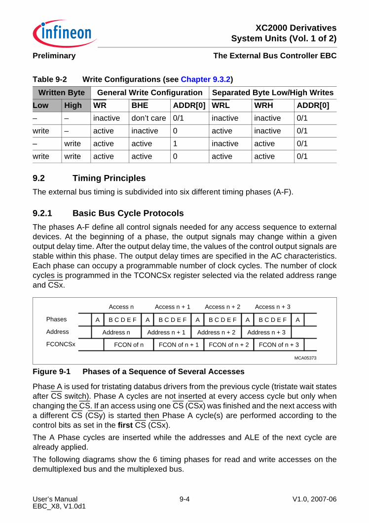
XC2000 DerivativesSystem Units (Vol. 1 of 2)
The External Bus Controller EBCPreliminary
9.2 Timing PrinciplesThe external bus timing is subdivided into six different timing phases (A-F).
9.2.1 Basic Bus Cycle ProtocolsThe phases A-F define all control signals needed for any access sequence to externaldevices. At the beginning of a phase, the output signals may change within a givenoutput delay time. After the output delay time, the values of the control output signals arestable within this phase. The output delay times are specified in the AC characteristics.Each phase can occupy a programmable number of clock cycles. The number of clockcycles is programmed in the TCONCSx register selected via the related address rangeand CSx.
Figure 9-1 Phases of a Sequence of Several Accesses
Phase A is used for tristating databus drivers from the previous cycle (tristate wait statesafter CS switch). Phase A cycles are not inserted at every access cycle but only whenchanging the CS. If an access using one CS (CSx) was finished and the next access witha different CS (CSy) is started then Phase A cycle(s) are performed according to thecontrol bits as set in the first CS (CSx).The A Phase cycles are inserted while the addresses and ALE of the next cycle arealready applied.The following diagrams show the 6 timing phases for read and write accesses on thedemultiplexed bus and the multiplexed bus.
Table 9-2 Write Configurations (see Chapter 9.3.2)Written Byte General Write Configuration Separated Byte Low/High Writes
Low High WR BHE ADDR[0] WRL WRH ADDR[0]– – inactive don’t care 0/1 inactive inactive 0/1write – active inactive 0 active inactive 0/1– write active active 1 inactive active 0/1write write active active 0 active active 0/1
B C D E F
MCA05373
Phases A A B C D E F A B C D E F A B C D E F A
Access n Access n + 1 Access n + 2 Access n + 3
Address n Address n + 1 Address n + 2 Address n + 3Address
FCON of n FCON of n + 1 FCON of n + 2 FCON of n + 3FCONCSx
User’s Manual 9-4 V1.0, 2007-06EBC_X8, V1.0d1
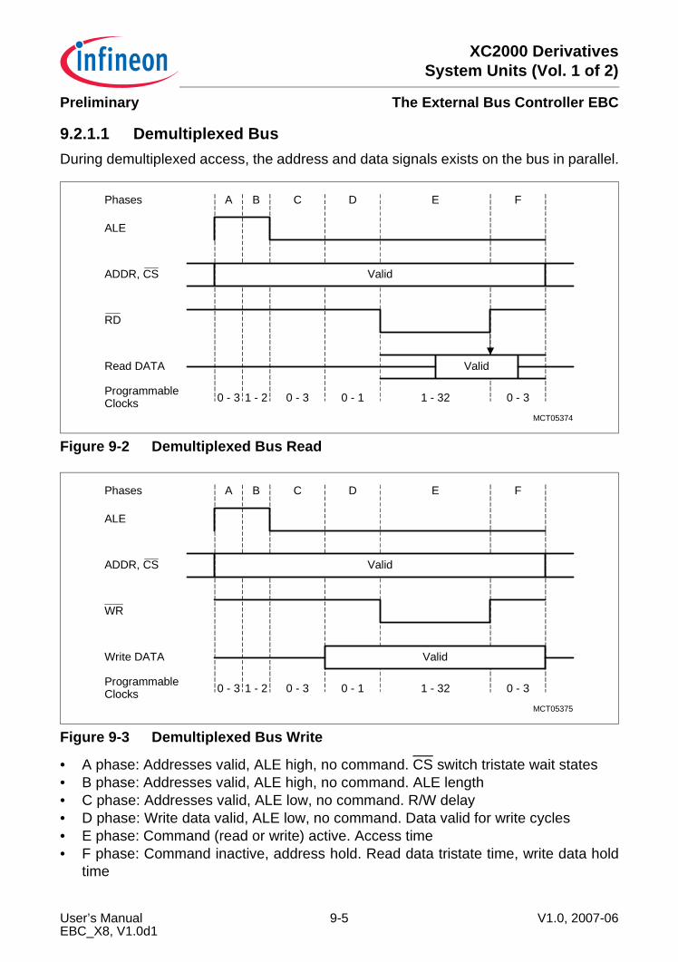
XC2000 DerivativesSystem Units (Vol. 1 of 2)
The External Bus Controller EBCPreliminary
9.2.1.1 Demultiplexed BusDuring demultiplexed access, the address and data signals exists on the bus in parallel.
Figure 9-2 Demultiplexed Bus Read
Figure 9-3 Demultiplexed Bus Write
• A phase: Addresses valid, ALE high, no command. CS switch tristate wait states• B phase: Addresses valid, ALE high, no command. ALE length• C phase: Addresses valid, ALE low, no command. R/W delay• D phase: Write data valid, ALE low, no command. Data valid for write cycles• E phase: Command (read or write) active. Access time• F phase: Command inactive, address hold. Read data tristate time, write data hold
time
MCT05374
A B C D E F
Valid
Valid
0 - 3 1 - 2 0 - 3 0 - 1 1 - 32 0 - 3
Phases
ALE
ADDR, CS
RD
Read DATA
ProgrammableClocks
MCT05375
A B C D E F
Valid
Valid
0 - 3 1 - 2 0 - 3 0 - 1 1 - 32 0 - 3
Phases
ALE
ADDR, CS
WR
Write DATA
ProgrammableClocks
User’s Manual 9-5 V1.0, 2007-06EBC_X8, V1.0d1
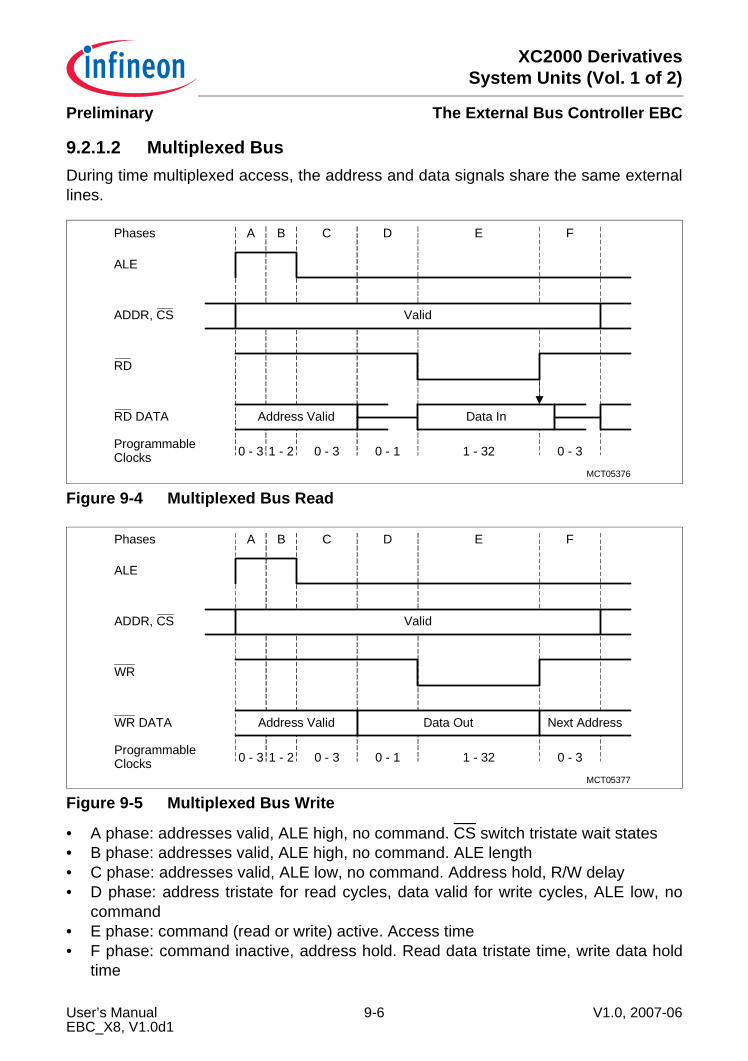
XC2000 DerivativesSystem Units (Vol. 1 of 2)
The External Bus Controller EBCPreliminary
9.2.1.2 Multiplexed BusDuring time multiplexed access, the address and data signals share the same externallines.
Figure 9-4 Multiplexed Bus Read
Figure 9-5 Multiplexed Bus Write
• A phase: addresses valid, ALE high, no command. CS switch tristate wait states• B phase: addresses valid, ALE high, no command. ALE length• C phase: addresses valid, ALE low, no command. Address hold, R/W delay• D phase: address tristate for read cycles, data valid for write cycles, ALE low, no
command• E phase: command (read or write) active. Access time• F phase: command inactive, address hold. Read data tristate time, write data hold
time
Address Valid
MCT05376
A B C D E F
Valid
Data In
0 - 3 1 - 2 0 - 3 0 - 1 1 - 32 0 - 3
Phases
ALE
ADDR, CS
RD
RD DATA
ProgrammableClocks
Next AddressAddress Valid
MCT05377
A B C D E F
Valid
Data Out
0 - 3 1 - 2 0 - 3 0 - 1 1 - 32 0 - 3
Phases
ALE
ADDR, CS
WR
WR DATA
ProgrammableClocks
User’s Manual 9-6 V1.0, 2007-06EBC_X8, V1.0d1
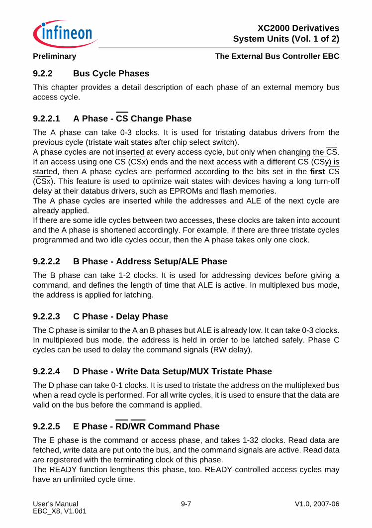
XC2000 DerivativesSystem Units (Vol. 1 of 2)
The External Bus Controller EBCPreliminary
9.2.2 Bus Cycle PhasesThis chapter provides a detail description of each phase of an external memory busaccess cycle.
9.2.2.1 A Phase - CS Change PhaseThe A phase can take 0-3 clocks. It is used for tristating databus drivers from theprevious cycle (tristate wait states after chip select switch).A phase cycles are not inserted at every access cycle, but only when changing the CS.If an access using one CS (CSx) ends and the next access with a different CS (CSy) isstarted, then A phase cycles are performed according to the bits set in the first CS(CSx). This feature is used to optimize wait states with devices having a long turn-offdelay at their databus drivers, such as EPROMs and flash memories.The A phase cycles are inserted while the addresses and ALE of the next cycle arealready applied.If there are some idle cycles between two accesses, these clocks are taken into accountand the A phase is shortened accordingly. For example, if there are three tristate cyclesprogrammed and two idle cycles occur, then the A phase takes only one clock.
9.2.2.2 B Phase - Address Setup/ALE PhaseThe B phase can take 1-2 clocks. It is used for addressing devices before giving acommand, and defines the length of time that ALE is active. In multiplexed bus mode,the address is applied for latching.
9.2.2.3 C Phase - Delay PhaseThe C phase is similar to the A an B phases but ALE is already low. It can take 0-3 clocks.In multiplexed bus mode, the address is held in order to be latched safely. Phase Ccycles can be used to delay the command signals (RW delay).
9.2.2.4 D Phase - Write Data Setup/MUX Tristate PhaseThe D phase can take 0-1 clocks. It is used to tristate the address on the multiplexed buswhen a read cycle is performed. For all write cycles, it is used to ensure that the data arevalid on the bus before the command is applied.
9.2.2.5 E Phase - RD/WR Command PhaseThe E phase is the command or access phase, and takes 1-32 clocks. Read data arefetched, write data are put onto the bus, and the command signals are active. Read dataare registered with the terminating clock of this phase.The READY function lengthens this phase, too. READY-controlled access cycles mayhave an unlimited cycle time.
User’s Manual 9-7 V1.0, 2007-06EBC_X8, V1.0d1
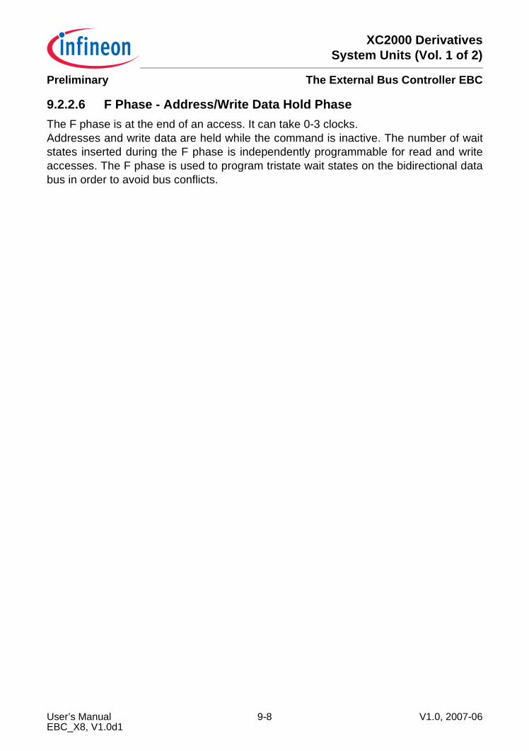
XC2000 DerivativesSystem Units (Vol. 1 of 2)
The External Bus Controller EBCPreliminary
9.2.2.6 F Phase - Address/Write Data Hold PhaseThe F phase is at the end of an access. It can take 0-3 clocks.Addresses and write data are held while the command is inactive. The number of waitstates inserted during the F phase is independently programmable for read and writeaccesses. The F phase is used to program tristate wait states on the bidirectional databus in order to avoid bus conflicts.
User’s Manual 9-8 V1.0, 2007-06EBC_X8, V1.0d1
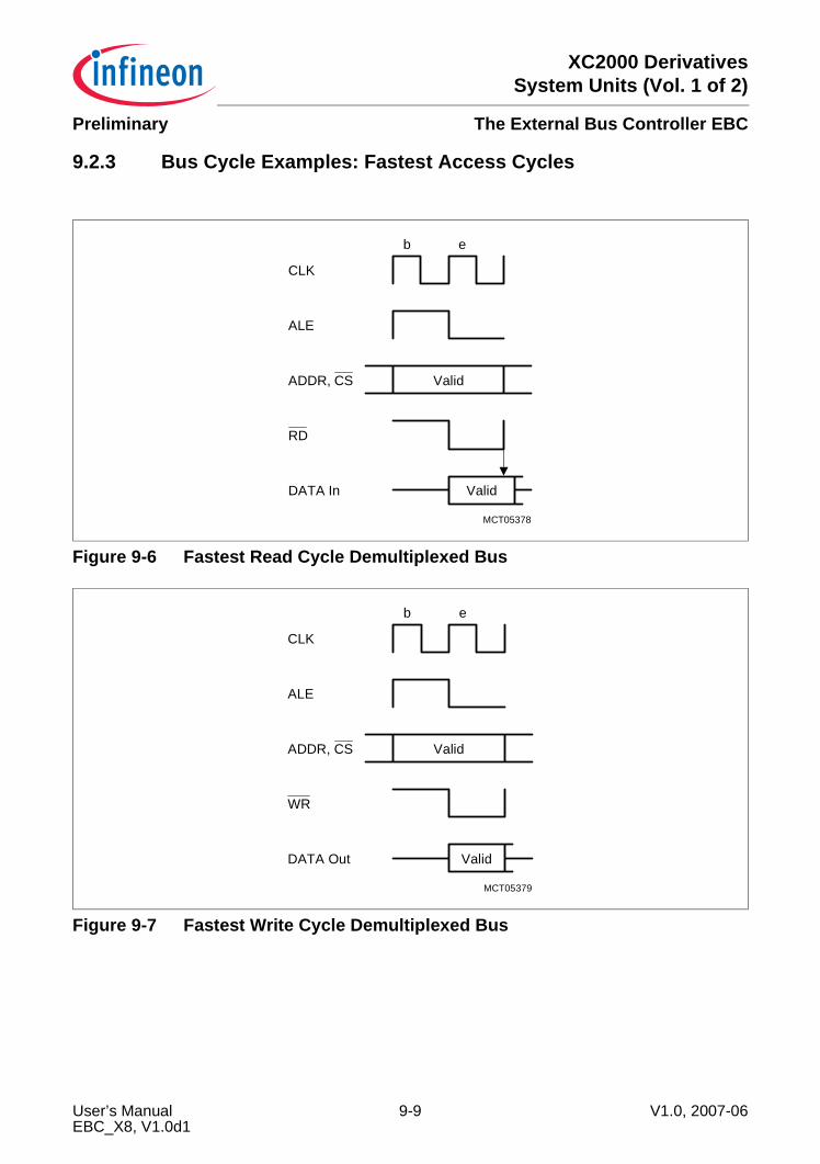
XC2000 DerivativesSystem Units (Vol. 1 of 2)
The External Bus Controller EBCPreliminary
9.2.3 Bus Cycle Examples: Fastest Access Cycles
Figure 9-6 Fastest Read Cycle Demultiplexed Bus
Figure 9-7 Fastest Write Cycle Demultiplexed Bus
MCT05378
b
CLK
e
ALE
ValidADDR, CS
RD
ValidDATA In
MCT05379
b
CLK
e
ALE
ValidADDR, CS
WR
ValidDATA Out
User’s Manual 9-9 V1.0, 2007-06EBC_X8, V1.0d1
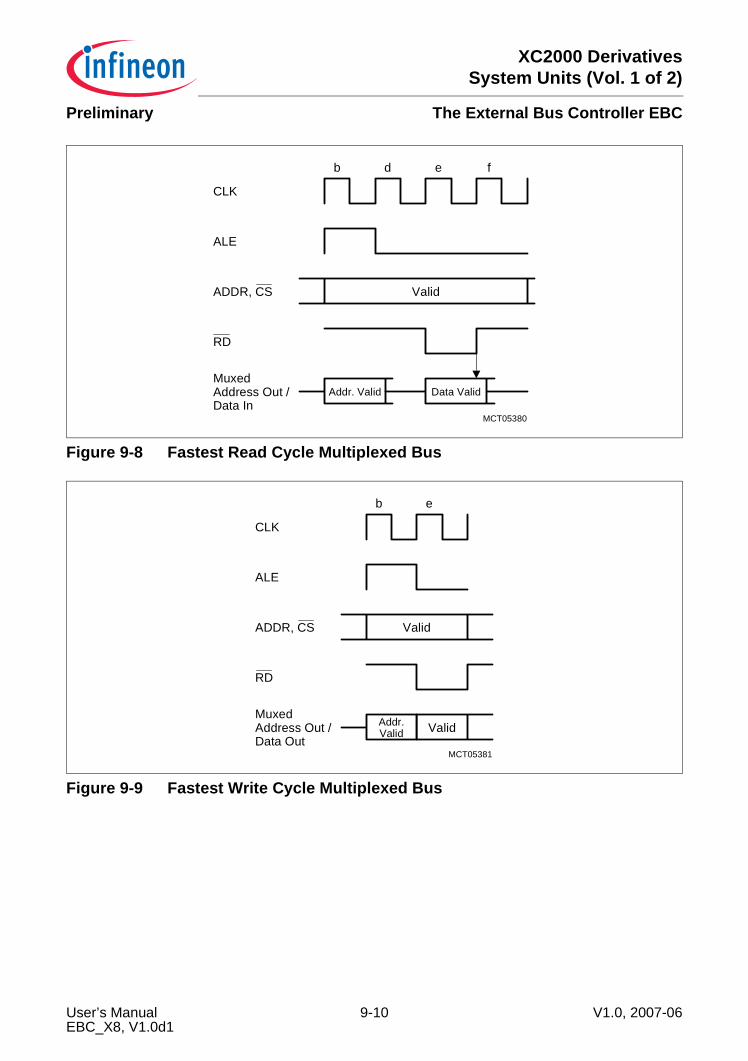
XC2000 DerivativesSystem Units (Vol. 1 of 2)
The External Bus Controller EBCPreliminary
Figure 9-8 Fastest Read Cycle Multiplexed Bus
Figure 9-9 Fastest Write Cycle Multiplexed Bus
MCT05380
b
CLK
d
ALE
ValidADDR, CS
RD
Data ValidMuxedAddress Out /Data In
e f
Addr. Valid
MCT05381
b
CLK
e
ALE
ValidADDR, CS
RD
ValidMuxedAddress Out /Data Out
Addr.Valid
User’s Manual 9-10 V1.0, 2007-06EBC_X8, V1.0d1
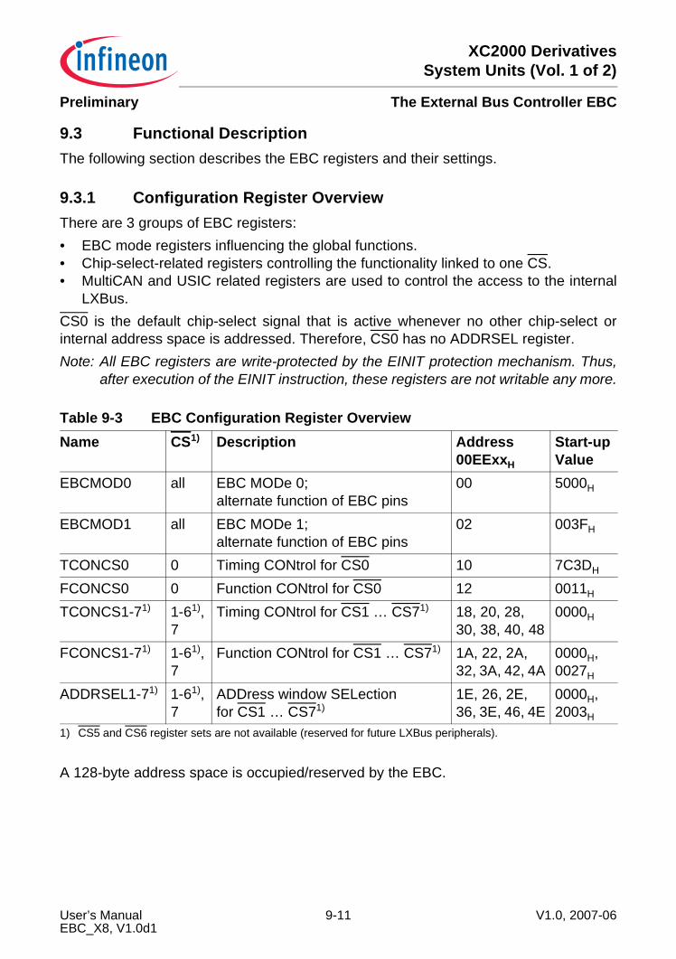
XC2000 DerivativesSystem Units (Vol. 1 of 2)
The External Bus Controller EBCPreliminary
9.3 Functional DescriptionThe following section describes the EBC registers and their settings.
9.3.1 Configuration Register OverviewThere are 3 groups of EBC registers:• EBC mode registers influencing the global functions.• Chip-select-related registers controlling the functionality linked to one CS.• MultiCAN and USIC related registers are used to control the access to the internal
LXBus.CS0 is the default chip-select signal that is active whenever no other chip-select orinternal address space is addressed. Therefore, CS0 has no ADDRSEL register.Note: All EBC registers are write-protected by the EINIT protection mechanism. Thus,
after execution of the EINIT instruction, these registers are not writable any more.
A 128-byte address space is occupied/reserved by the EBC.
Table 9-3 EBC Configuration Register OverviewName CS1)
1) CS5 and CS6 register sets are not available (reserved for future LXBus peripherals).
Description Address00EExxH
Start-up Value
EBCMOD0 all EBC MODe 0;alternate function of EBC pins
00 5000H
EBCMOD1 all EBC MODe 1;alternate function of EBC pins
02 003FH
TCONCS0 0 Timing CONtrol for CS0 10 7C3DH
FCONCS0 0 Function CONtrol for CS0 12 0011H
TCONCS1-71) 1-61), 7
Timing CONtrol for CS1 … CS71) 18, 20, 28, 30, 38, 40, 48
0000H
FCONCS1-71) 1-61), 7
Function CONtrol for CS1 … CS71) 1A, 22, 2A, 32, 3A, 42, 4A
0000H, 0027H
ADDRSEL1-71) 1-61), 7
ADDress window SELectionfor CS1 … CS71)
1E, 26, 2E, 36, 3E, 46, 4E
0000H, 2003H
User’s Manual 9-11 V1.0, 2007-06EBC_X8, V1.0d1
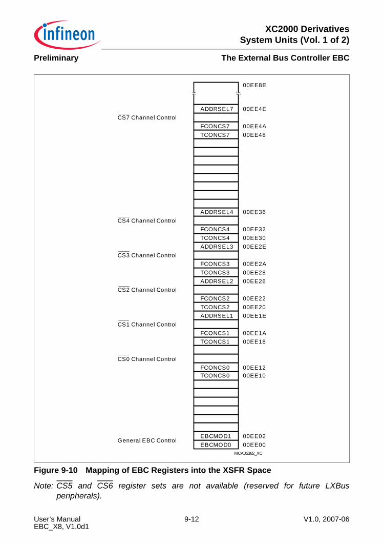
XC2000 DerivativesSystem Units (Vol. 1 of 2)
The External Bus Controller EBCPreliminary
Figure 9-10 Mapping of EBC Registers into the XSFR Space
Note: CS5 and CS6 register sets are not available (reserved for future LXBusperipherals).
MCA05382_XC
EBCMOD0EBCMOD1
TCONCS0FCONCS0
TCONCS1FCONCS1
ADDRSEL1TCONCS2FCONCS2
ADDRSEL2TCONCS3FCONCS3
ADDRSEL3
TCONCS7FCONCS7
ADDRSEL7
00EE0000EE02
00EE1000EE12
00EE1800EE1A
00EE1E00EE2000EE22
00EE2600EE2800EE2A
00EE2E
00EE4800EE4A
00EE4E
00EE8E
General EBC Control
CS0 Channel Control
CS1 Channel Control
CS2 Channel Control
CS3 Channel Control
CS7 Channel Control
TCONCS4FCONCS4
ADDRSEL4
00EE3000EE32
00EE36CS4 Channel Control
User’s Manual 9-12 V1.0, 2007-06EBC_X8, V1.0d1
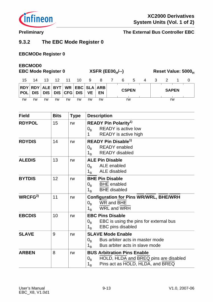
XC2000 DerivativesSystem Units (Vol. 1 of 2)
The External Bus Controller EBCPreliminary
9.3.2 The EBC Mode Register 0
EBCMODe Register 0
EBCMOD0 EBC Mode Register 0 XSFR (EE00H/--) Reset Value: 5000H
15 14 13 12 11 10 9 8 7 6 5 4 3 2 1 0
RDY POL
RDY DIS
ALE DIS
BYT DIS
WR CFG
EBC DIS
SLA VE
ARB EN CSPEN SAPEN
rw rw rw rw rw rw rw rw rw rw
Field Bits Type DescriptionRDYPOL 15 rw READY Pin Polarity1)
0B READY is active low1 READY is active high
RDYDIS 14 rw READY Pin Disable1)
0B READY enabled1B READY disabled
ALEDIS 13 rw ALE Pin Disable0B ALE enabled1B ALE disabled
BYTDIS 12 rw BHE Pin Disable0B BHE enabled1B BHE disabled
WRCFG2) 11 rw Configuration for Pins WR/WRL, BHE/WRH0B WR and BHE1B WRL and WRH
EBCDIS 10 rw EBC Pins Disable0B EBC is using the pins for external bus1B EBC pins disabled
SLAVE 9 rw SLAVE Mode Enable0B Bus arbiter acts in master mode1B Bus arbiter acts in slave mode
ARBEN 8 rw BUS Arbitration Pins Enable0B HOLD, HLDA and BREQ pins are disabled1B Pins act as HOLD, HLDA, and BREQ
User’s Manual 9-13 V1.0, 2007-06EBC_X8, V1.0d1
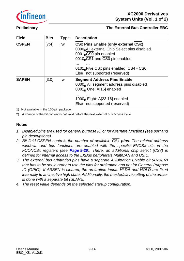
XC2000 DerivativesSystem Units (Vol. 1 of 2)
The External Bus Controller EBCPreliminary
Notes1. Disabled pins are used for general purpose IO or for alternate functions (see port and
pin descriptions).2. Bit field CSPEN controls the number of available CSx pins. The related address
windows and bus functions are enabled with the specific ENCSx bits in theFCONCSx registers (see Page 9-20). There, an additional chip select (CS7) isdefined for internal access to the LXBus peripherals MultiCAN and USIC.
3. The external bus arbitration pins have a separate ARBitration ENable bit (ARBEN)that has to be set in order to use the pins for arbitration and not for General PurposeIO (GPIO). If ARBEN is cleared, the arbitration inputs HLDA and HOLD are fixedinternally to an inactive high state. Additionally, the master/slave setting of the arbiteris done with a separate bit (SLAVE).
4. The reset value depends on the selected startup configuration.
CSPEN [7:4] rw CSx Pins Enable (only external CSx)0000BAll external Chip Select pins disabled.0001BCS0 pin enabled0010BCS1 and CS0 pin enabled… …0101BFive CSx pins enabled: CS4 - CS0Else not supported (reserved)
SAPEN [3:0] rw Segment Address Pins Enable0000B All segment address pins disabled0001B One: A[16] enabled… …1000B Eight: A[23:16] enabledElse not supported (reserved)
1) Not available in the 100-pin package.2) A change of the bit content is not valid before the next external bus access cycle.
Field Bits Type Description
User’s Manual 9-14 V1.0, 2007-06EBC_X8, V1.0d1

XC2000 DerivativesSystem Units (Vol. 1 of 2)
The External Bus Controller EBCPreliminary
9.3.3 The EBC Mode Register 1EBC MODe register 1 controls the general use of port pins for external bus.
Notes1. Disabled bus pins may be used for general purpose IO or for alternate functions (see
port and pin descriptions).2. After reset, the address and data bus pins are enabled, but in Idle state.
EBCMOD1 EBC Mode Register 1 XSFR (EE02H/--) Reset Value: 003FH
15 14 13 12 11 10 9 8 7 6 5 4 3 2 1 0
- - - - - - - - WRPDIS
DHPDIS
ALPDIS
A0PDIS APDIS
- - - - - - - - rw rw rw rw rw
Field Bits Type DescriptionWRPDIS 7 rw WR/WRL Pin Disable
0B WR/WRL pin enabled1B WR/WRL pin disabled
DHPDIS 6 rw Data High Port Pins Disable0B Address/Data bus pins 15-8 enabled1B Address/Data bus pins 15-8 disabled
ALPDIS 5 rw Address Low Pins Disable0B Address bus pins 7-0 generally enabled
(depending on APDIS/A0PDIS)1B Address bus pins 7-0 disabled
A0PDIS 4 rw Address Bit 0 Pin Disable0B Address bus pin 0 enabled1B Address bus pin 0 disabled
APDIS [3:0] rw Address Port Pins Disable0000B Address bus pins 15-1 enabled0001B Pin A15 disabled, A14-A1 enabled0010B Pins A15-A14 disabled, A13-A1 enabled0011B Pins A15-A13 disabled, A12-A1 enabled… …1110B Pins A15-A2 disabled, A1 enabled1111B Address bus pins 15-1 disabled
User’s Manual 9-15 V1.0, 2007-06EBC_X8, V1.0d1
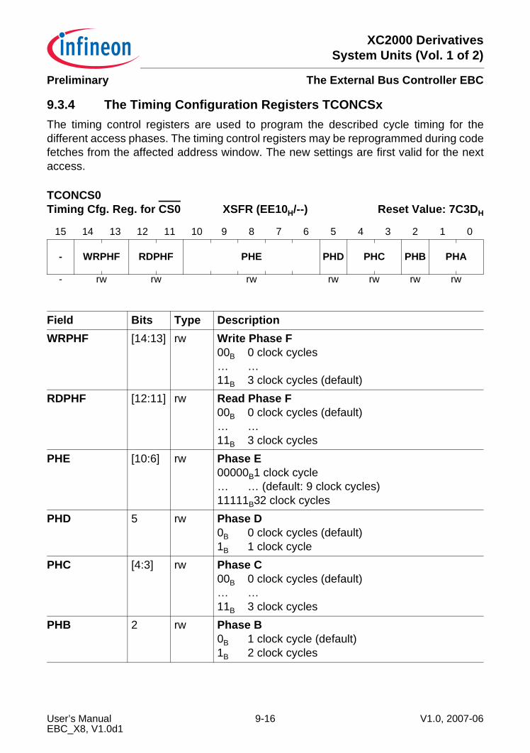
XC2000 DerivativesSystem Units (Vol. 1 of 2)
The External Bus Controller EBCPreliminary
9.3.4 The Timing Configuration Registers TCONCSxThe timing control registers are used to program the described cycle timing for thedifferent access phases. The timing control registers may be reprogrammed during codefetches from the affected address window. The new settings are first valid for the nextaccess.
TCONCS0 Timing Cfg. Reg. for CS0 XSFR (EE10H/--) Reset Value: 7C3DH
15 14 13 12 11 10 9 8 7 6 5 4 3 2 1 0
- WRPHF RDPHF PHE PHD PHC PHB PHA
- rw rw rw rw rw rw rw
Field Bits Type DescriptionWRPHF [14:13] rw Write Phase F
00B 0 clock cycles… …11B 3 clock cycles (default)
RDPHF [12:11] rw Read Phase F00B 0 clock cycles (default)… …11B 3 clock cycles
PHE [10:6] rw Phase E00000B1 clock cycle… … (default: 9 clock cycles)11111B32 clock cycles
PHD 5 rw Phase D0B 0 clock cycles (default)1B 1 clock cycle
PHC [4:3] rw Phase C00B 0 clock cycles (default)… …11B 3 clock cycles
PHB 2 rw Phase B0B 1 clock cycle (default)1B 2 clock cycles
User’s Manual 9-16 V1.0, 2007-06EBC_X8, V1.0d1
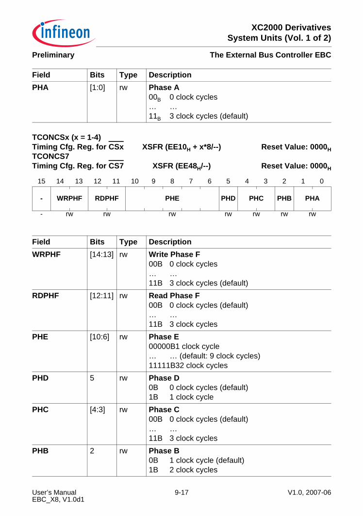
XC2000 DerivativesSystem Units (Vol. 1 of 2)
The External Bus Controller EBCPreliminary
PHA [1:0] rw Phase A00B 0 clock cycles… …11B 3 clock cycles (default)
TCONCSx (x = 1-4) Timing Cfg. Reg. for CSx XSFR (EE10H + x*8/--) Reset Value: 0000HTCONCS7 Timing Cfg. Reg. for CS7 XSFR (EE48H/--) Reset Value: 0000H
15 14 13 12 11 10 9 8 7 6 5 4 3 2 1 0
- WRPHF RDPHF PHE PHD PHC PHB PHA
- rw rw rw rw rw rw rw
Field Bits Type DescriptionWRPHF [14:13] rw Write Phase F
00B 0 clock cycles… …11B 3 clock cycles (default)
RDPHF [12:11] rw Read Phase F00B 0 clock cycles (default)… …11B 3 clock cycles
PHE [10:6] rw Phase E00000B1 clock cycle… … (default: 9 clock cycles)11111B32 clock cycles
PHD 5 rw Phase D0B 0 clock cycles (default)1B 1 clock cycle
PHC [4:3] rw Phase C00B 0 clock cycles (default)… …11B 3 clock cycles
PHB 2 rw Phase B0B 1 clock cycle (default)1B 2 clock cycles
Field Bits Type Description
User’s Manual 9-17 V1.0, 2007-06EBC_X8, V1.0d1
XC2000 DerivativesSystem Units (Vol. 1 of 2)
The External Bus Controller EBCPreliminary
Note: x = 7 belongs to the additional chip select (CS7) which is used and defined forinternal access to the LXBus peripherals MultiCAN and USIC. The registerTCONCS4 controls the chip select CS4, that is available only in the 144-pinpackage.
PHA [1:0] rw Phase A00B 0 clock cycles… …11B 3 clock cycles (default)
Field Bits Type Description
User’s Manual 9-18 V1.0, 2007-06EBC_X8, V1.0d1
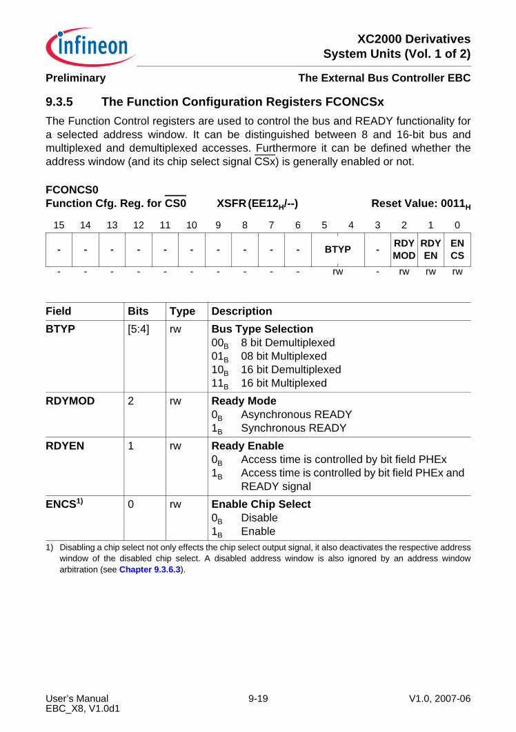
XC2000 DerivativesSystem Units (Vol. 1 of 2)
The External Bus Controller EBCPreliminary
9.3.5 The Function Configuration Registers FCONCSxThe Function Control registers are used to control the bus and READY functionality fora selected address window. It can be distinguished between 8 and 16-bit bus andmultiplexed and demultiplexed accesses. Furthermore it can be defined whether theaddress window (and its chip select signal CSx) is generally enabled or not.
FCONCS0 Function Cfg. Reg. for CS0 XSFR (EE12H/--) Reset Value: 0011H
15 14 13 12 11 10 9 8 7 6 5 4 3 2 1 0
- - - - - - - - - - BTYP - RDY MOD
RDYEN
ENCS
- - - - - - - - - - rw - rw rw rw
Field Bits Type DescriptionBTYP [5:4] rw Bus Type Selection
00B 8 bit Demultiplexed01B 08 bit Multiplexed10B 16 bit Demultiplexed11B 16 bit Multiplexed
RDYMOD 2 rw Ready Mode0B Asynchronous READY1B Synchronous READY
RDYEN 1 rw Ready Enable0B Access time is controlled by bit field PHEx1B Access time is controlled by bit field PHEx and
READY signalENCS1)
1) Disabling a chip select not only effects the chip select output signal, it also deactivates the respective addresswindow of the disabled chip select. A disabled address window is also ignored by an address windowarbitration (see Chapter 9.3.6.3).
0 rw Enable Chip Select0B Disable1B Enable
User’s Manual 9-19 V1.0, 2007-06EBC_X8, V1.0d1
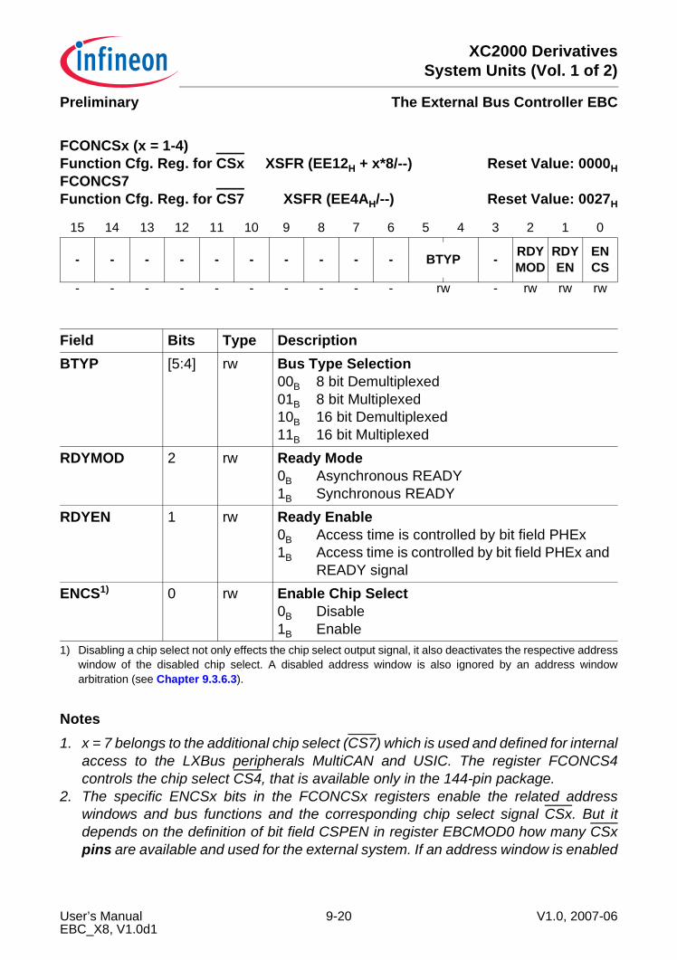
XC2000 DerivativesSystem Units (Vol. 1 of 2)
The External Bus Controller EBCPreliminary
Notes1. x = 7 belongs to the additional chip select (CS7) which is used and defined for internal
access to the LXBus peripherals MultiCAN and USIC. The register FCONCS4controls the chip select CS4, that is available only in the 144-pin package.
2. The specific ENCSx bits in the FCONCSx registers enable the related addresswindows and bus functions and the corresponding chip select signal CSx. But itdepends on the definition of bit field CSPEN in register EBCMOD0 how many CSxpins are available and used for the external system. If an address window is enabled
FCONCSx (x = 1-4) Function Cfg. Reg. for CSx XSFR (EE12H + x*8/--) Reset Value: 0000HFCONCS7Function Cfg. Reg. for CS7 XSFR (EE4AH/--) Reset Value: 0027H
15 14 13 12 11 10 9 8 7 6 5 4 3 2 1 0
- - - - - - - - - - BTYP - RDY MOD
RDY EN
ENCS
- - - - - - - - - - rw - rw rw rw
Field Bits Type DescriptionBTYP [5:4] rw Bus Type Selection
00B 8 bit Demultiplexed01B 8 bit Multiplexed10B 16 bit Demultiplexed11B 16 bit Multiplexed
RDYMOD 2 rw Ready Mode0B Asynchronous READY1B Synchronous READY
RDYEN 1 rw Ready Enable0B Access time is controlled by bit field PHEx1B Access time is controlled by bit field PHEx and
READY signalENCS1)
1) Disabling a chip select not only effects the chip select output signal, it also deactivates the respective addresswindow of the disabled chip select. A disabled address window is also ignored by an address windowarbitration (see Chapter 9.3.6.3).
0 rw Enable Chip Select0B Disable1B Enable
User’s Manual 9-20 V1.0, 2007-06EBC_X8, V1.0d1
XC2000 DerivativesSystem Units (Vol. 1 of 2)
The External Bus Controller EBCPreliminary
but no external pin is available for the CSx, the external bus cycle is executed withoutchip select signal.
3. With ENCS7 the chip select CS7 and its related register set is enabled and definedfor internal access to the LXBus peripherals MultiCAN and USIC.
User’s Manual 9-21 V1.0, 2007-06EBC_X8, V1.0d1
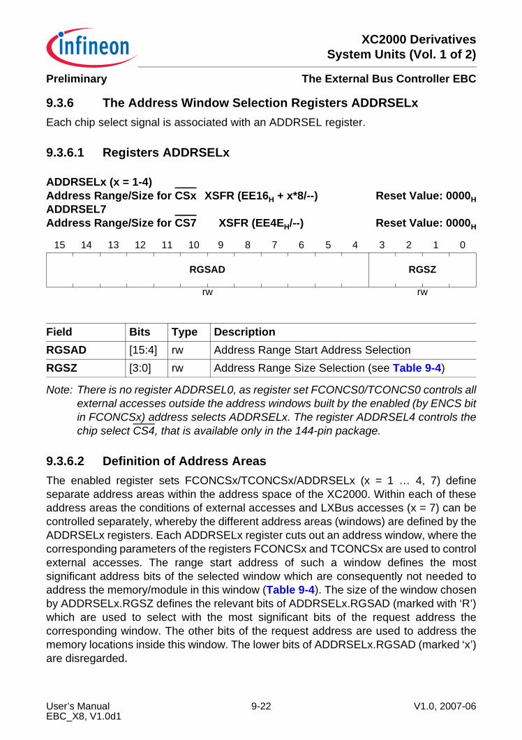
XC2000 DerivativesSystem Units (Vol. 1 of 2)
The External Bus Controller EBCPreliminary
9.3.6 The Address Window Selection Registers ADDRSELxEach chip select signal is associated with an ADDRSEL register.
9.3.6.1 Registers ADDRSELx
Note: There is no register ADDRSEL0, as register set FCONCS0/TCONCS0 controls allexternal accesses outside the address windows built by the enabled (by ENCS bitin FCONCSx) address selects ADDRSELx. The register ADDRSEL4 controls thechip select CS4, that is available only in the 144-pin package.
9.3.6.2 Definition of Address AreasThe enabled register sets FCONCSx/TCONCSx/ADDRSELx (x = 1 … 4, 7) defineseparate address areas within the address space of the XC2000. Within each of theseaddress areas the conditions of external accesses and LXBus accesses (x = 7) can becontrolled separately, whereby the different address areas (windows) are defined by theADDRSELx registers. Each ADDRSELx register cuts out an address window, where thecorresponding parameters of the registers FCONCSx and TCONCSx are used to controlexternal accesses. The range start address of such a window defines the mostsignificant address bits of the selected window which are consequently not needed toaddress the memory/module in this window (Table 9-4). The size of the window chosenby ADDRSELx.RGSZ defines the relevant bits of ADDRSELx.RGSAD (marked with ‘R’)which are used to select with the most significant bits of the request address thecorresponding window. The other bits of the request address are used to address thememory locations inside this window. The lower bits of ADDRSELx.RGSAD (marked ‘x’)are disregarded.
ADDRSELx (x = 1-4) Address Range/Size for CSx XSFR (EE16H + x*8/--) Reset Value: 0000HADDRSEL7 Address Range/Size for CS7 XSFR (EE4EH/--) Reset Value: 0000H
15 14 13 12 11 10 9 8 7 6 5 4 3 2 1 0
RGSAD RGSZ
rw rw
Field Bits Type DescriptionRGSAD [15:4] rw Address Range Start Address SelectionRGSZ [3:0] rw Address Range Size Selection (see Table 9-4)
User’s Manual 9-22 V1.0, 2007-06EBC_X8, V1.0d1
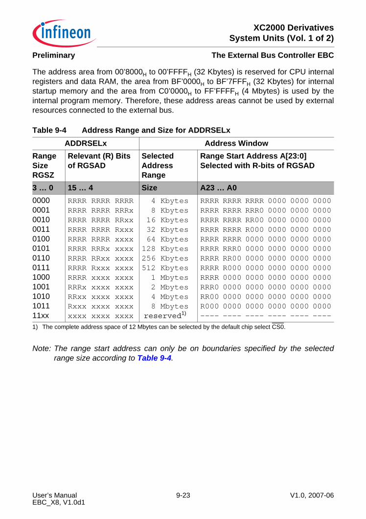
XC2000 DerivativesSystem Units (Vol. 1 of 2)
The External Bus Controller EBCPreliminary
The address area from 00’8000H to 00’FFFFH (32 Kbytes) is reserved for CPU internalregisters and data RAM, the area from BF’0000H to BF’7FFFH (32 Kbytes) for internalstartup memory and the area from C0’0000H to FF’FFFFH (4 Mbytes) is used by theinternal program memory. Therefore, these address areas cannot be used by externalresources connected to the external bus.
Note: The range start address can only be on boundaries specified by the selectedrange size according to Table 9-4.
Table 9-4 Address Range and Size for ADDRSELxADDRSELx Address Window
Range SizeRGSZ
Relevant (R) Bits of RGSAD
Selected Address Range
Range Start Address A[23:0] Selected with R-bits of RGSAD
3 … 0 15 … 4 Size A23 … A000000001001000110100010101100111100010011010101111xx
RRRR RRRR RRRRRRRR RRRR RRRxRRRR RRRR RRxxRRRR RRRR RxxxRRRR RRRR xxxxRRRR RRRx xxxxRRRR RRxx xxxxRRRR Rxxx xxxxRRRR xxxx xxxxRRRx xxxx xxxxRRxx xxxx xxxxRxxx xxxx xxxxxxxx xxxx xxxx
4 Kbytes 8 Kbytes 16 Kbytes 32 Kbytes 64 Kbytes128 Kbytes256 Kbytes512 Kbytes 1 Mbytes 2 Mbytes 4 Mbytes 8 Mbytes reserved1)
1) The complete address space of 12 Mbytes can be selected by the default chip select CS0.
RRRR RRRR RRRR 0000 0000 0000RRRR RRRR RRR0 0000 0000 0000RRRR RRRR RR00 0000 0000 0000RRRR RRRR R000 0000 0000 0000RRRR RRRR 0000 0000 0000 0000RRRR RRR0 0000 0000 0000 0000RRRR RR00 0000 0000 0000 0000RRRR R000 0000 0000 0000 0000RRRR 0000 0000 0000 0000 0000RRR0 0000 0000 0000 0000 0000RR00 0000 0000 0000 0000 0000R000 0000 0000 0000 0000 0000---- ---- ---- ---- ---- ----
User’s Manual 9-23 V1.0, 2007-06EBC_X8, V1.0d1
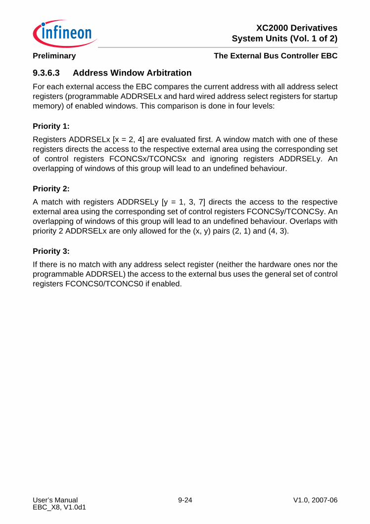
XC2000 DerivativesSystem Units (Vol. 1 of 2)
The External Bus Controller EBCPreliminary
9.3.6.3 Address Window ArbitrationFor each external access the EBC compares the current address with all address selectregisters (programmable ADDRSELx and hard wired address select registers for startupmemory) of enabled windows. This comparison is done in four levels:
Priority 1:Registers ADDRSELx [x = 2, 4] are evaluated first. A window match with one of theseregisters directs the access to the respective external area using the corresponding setof control registers FCONCSx/TCONCSx and ignoring registers ADDRSELy. Anoverlapping of windows of this group will lead to an undefined behaviour.
Priority 2:A match with registers ADDRSELy [y = 1, 3, 7] directs the access to the respectiveexternal area using the corresponding set of control registers FCONCSy/TCONCSy. Anoverlapping of windows of this group will lead to an undefined behaviour. Overlaps withpriority 2 ADDRSELx are only allowed for the (x, y) pairs (2, 1) and (4, 3).
Priority 3:If there is no match with any address select register (neither the hardware ones nor theprogrammable ADDRSEL) the access to the external bus uses the general set of controlregisters FCONCS0/TCONCS0 if enabled.
User’s Manual 9-24 V1.0, 2007-06EBC_X8, V1.0d1
XC2000 DerivativesSystem Units (Vol. 1 of 2)
The External Bus Controller EBCPreliminary
9.3.7 Ready Controlled Bus CyclesIn cases, where the response (access) time of a peripheral is not constant, or where theprogrammable wait states are not enough, the EBC provides external bus cycles that areterminated via a READY input signal.
9.3.7.1 GeneralIn such cases during phase E the EBC first counts a programmable number of clockcycles (1 … 32) and then starts in the last wait cycle to monitor the internal READY line(see Figure 9-11) to determine the actual end of the current bus cycle. The externaldevice drives READY active in order to indicate that data has been latched (write cycle)or is available (read cycle).The READY pin is generally enabled by setting the bit RDYDIS in EBCMOD0 to ‘0’ inorder to switch the corresponding port pin. Also the polarity of the READY is definedinside the EBCMOD0 register on the RDYPOL bit.For a specific address window the READY function is enabled via the RDYEN bit in theFCONCSx register. With FCONCSx.RDYMOD the READY is handled either insynchronous or in asynchronous mode (see also Figure 9-11).When the READY function is enabled for a specific address window, each bus cyclewithin this window must be terminated with an active READY signal. Otherwise thecontroller hangs until the next reset. This is also the case for an enabled RDYEN but adisabled READY port pin.
Figure 9-11 External to Internal READY Conversion
MCA05383
1READY Ext
EBCMOD0.RDYPOL
Async.
FCONCSx.RDYMODx
Sync. READY Int
MUX0
1
MUX0
1
User’s Manual 9-25 V1.0, 2007-06EBC_X8, V1.0d1

XC2000 DerivativesSystem Units (Vol. 1 of 2)
The External Bus Controller EBCPreliminary
9.3.7.2 The Synchronous/Asynchronous READYThe synchronous READY provides the fastest bus cycles, but requires setup and holdtimes to be met. The CLKOUT signal should be enabled and may be used by theperipheral logic to control the READY timing in this case.The asynchronous READY is less restrictive, but requires one additional wait statecaused by the internal synchronization. As the asynchronous READY is sampled earlierprogrammed wait states may be necessary to provide proper bus cycles.A READY signal (especially asynchronous READY) that has been activated by anexternal device may be deactivated in response to the trailing (rising) edge of therespective command (RD or WR).
Figure 9-12 READY Controlled Bus Cycles
9.3.7.3 Combining the READY Function with Predefined Wait StatesTypically an external wait state or READY control logic takes a while to generate theREADY signal when a cycle was started. After a predefined number of clock cycles theEBC will start checking its READY line to determine the end of the bus cycle.When using the READY function with so-called ‘normally-ready’ peripherals, it may leadto erroneous bus cycles, if the READY line is sampled too early. These peripherals pulltheir READY output active, while they are idle. When they are accessed, they driveREADY inactive until the bus cycle is complete, then drive it active again. If, however,the peripheral drives READY inactive a little late, after the first sample point of theXC2000, the controller samples an active READY and terminates the current bus cycle
Programmedphase E
wait states
Programmedphase E
wait states
MCT05384
Bus Cycle with Active READY Bus Cycle Extended via READY
ALE
RD / WR
Sync. READY
Async. READY
Sampling of READY Input Not Interesting READY Cycles
User’s Manual 9-26 V1.0, 2007-06EBC_X8, V1.0d1
XC2000 DerivativesSystem Units (Vol. 1 of 2)
The External Bus Controller EBCPreliminary
too early. By inserting predefined wait states the first READY sample point can be shiftedto a time, where the peripheral has safely controlled the READY line.
9.3.8 Access Control to LXBus ModulesAccess control to LXBus is required for accesses to the MultiCAN and USIC module. Ingeneral, accesses to LXBus are not visible on external bus. During LXBus cycles, theexternal bus is still enabled, but driven to inactive states (control signals) or switched intothe read mode (busses).For accesses to MultiCAN and USICs, CS7 and its control registers ADDRSEL7,TCONCS7, and FCONCS7 are used. The selection of LXBus is controlled with CS7. Theaddress range, defined in ADDRSEL7, is located in the ’External IO Range’ (range from20’0000H to 3F’FFFFH). Only for the External IO Range of the total external addressrange it is guaranteed, that a read access is executed after a preceding write access.The value of the bus function control register FCONCS7 is selected according to therequirements of the MultiCAN and USIC: 16-bit demultiplexed bus, access timecontrolled with synchronous READY. This function control is represented by the defaultvalue for FCONCS7 of ’0027H’.The LXBus cycle timing as controlled with register TCONCS7 the shortest possibletiming using two clock cycles for one bus cycle. But this minimum timing will belengthened with waitstate(s) controlled by the MultiCAN/USIC itself with the READYfunction. This timing control is controlled by the reset value of TCONCS7 (’0000H’).
User’s Manual 9-27 V1.0, 2007-06EBC_X8, V1.0d1
XC2000 DerivativesSystem Units (Vol. 1 of 2)
The External Bus Controller EBCPreliminary
9.3.9 External Bus ArbitrationThe XC2000 supports multi master systems on the external bus by its external busarbitration. This bus arbitration allows an external master to request the external bus.The XC2000 will release the external bus and will float the data and address bus linesand force the control signals via pull-ups/downs to their inactive state.
9.3.9.1 Initialization of ArbitrationDuring reset all arbitration pins are tristate, except pin BREQ which is pulled inactive.After reset the XC2000 EBC always starts in ‘init mode’ where the external bus isavailable but no arbitration is enabled. All arbitration pins are ignored in this state. Otherto the external bus connected XC2000 EBCs assume to have the bus also, so potentialbus conflicts are not resolved. For a multi master system the arbitration should beinitialized first before starting any bus access. The EBC can either be chosen asarbitration master or as arbitration slave by programming the EBCMOD0 bit SLAVE. Theselected mode and the arbitration gets active by the first setting of the HLDEN bit insidethe CPUs PSW register. Afterwards a change of the slave/master mode is not possiblewithout resetting the device. Of course for arbitration the dedicated pins have to beactivated by setting EBCMOD0.ARBEN.
9.3.9.2 Arbitration Master SchemeIf the XC2000 EBC is configured as arbitration master, it is default owner of the externalbus, controls the arbitration protocol and drives the bus also during idle phases with nobus requests. To perform the arbitration handshake a HOLD input allows the request ofthe external bus from the arbitration master. When the arbitration master hands over thebus to the requester this is signaled by driving the hold acknowledge pin HLDA low,which remains at this level until the arbitration slave frees the bus by releasing its requeston the HOLD input. If the arbitration master is not the owner of the bus it treats theexternal bus interface as follows:• Address and data bus(es) float to tristate• Command lines are pulled high by internal pull-up devices (RD, WR/WRL,
BHE/WRH)• Address latch control line ALE is pulled low by an internal pull-down device• CSx outputs are pulled high by internal pull-up devices.In this state the arbitration slave can take over the bus.If the arbitration master requires the bus again, it can request the bus via the bus requestsignal BREQ. As soon as the arbitration master regains the bus it releases the BREQsignal and drives HLDA to high.
User’s Manual 9-28 V1.0, 2007-06EBC_X8, V1.0d1
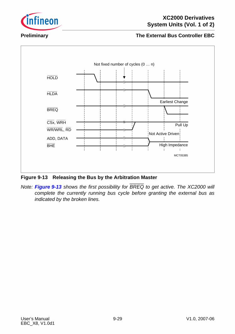
XC2000 DerivativesSystem Units (Vol. 1 of 2)
The External Bus Controller EBCPreliminary
Figure 9-13 Releasing the Bus by the Arbitration Master
Note: Figure 9-13 shows the first possibility for BREQ to get active. The XC2000 willcomplete the currently running bus cycle before granting the external bus asindicated by the broken lines.
MCT05385
Not fixed number of cycles (0 … n)
HOLD
HLDA
BREQ
CSx, WRH
WR/WRL, RD
ADD, DATA
BHE
Earliest Change
Not Active Driven
Pull Up
High Impedance
User’s Manual 9-29 V1.0, 2007-06EBC_X8, V1.0d1
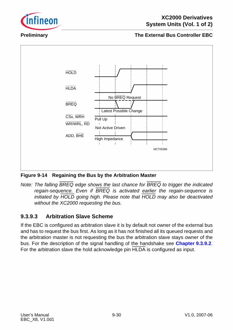
XC2000 DerivativesSystem Units (Vol. 1 of 2)
The External Bus Controller EBCPreliminary
Figure 9-14 Regaining the Bus by the Arbitration Master
Note: The falling BREQ edge shows the last chance for BREQ to trigger the indicatedregain-sequence. Even if BREQ is activated earlier the regain-sequence isinitiated by HOLD going high. Please note that HOLD may also be deactivatedwithout the XC2000 requesting the bus.
9.3.9.3 Arbitration Slave SchemeIf the EBC is configured as arbitration slave it is by default not owner of the external busand has to request the bus first. As long as it has not finished all its queued requests andthe arbitration master is not requesting the bus the arbitration slave stays owner of thebus. For the description of the signal handling of the handshake see Chapter 9.3.9.2.For the arbitration slave the hold acknowledge pin HLDA is configured as input.
MCT05386
HOLD
HLDA
BREQ
CSx, WRH
WR/WRL, RD
ADD, BHE
Not Active Driven
Pull Up
High Impedance
Latest Possible Change
No BREQ Request
User’s Manual 9-30 V1.0, 2007-06EBC_X8, V1.0d1
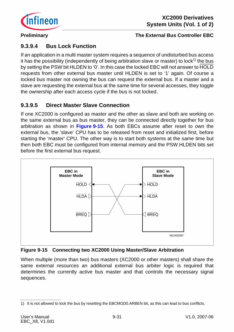
XC2000 DerivativesSystem Units (Vol. 1 of 2)
The External Bus Controller EBCPreliminary
9.3.9.4 Bus Lock FunctionIf an application in a multi master system requires a sequence of undisturbed bus accessit has the possibility (independently of being arbitration slave or master) to lock1) the busby setting the PSW bit HLDEN to ‘0’. In this case the locked EBC will not answer to HOLDrequests from other external bus master until HLDEN is set to ‘1’ again. Of course alocked bus master not owning the bus can request the external bus. If a master and aslave are requesting the external bus at the same time for several accesses, they togglethe ownership after each access cycle if the bus is not locked.
9.3.9.5 Direct Master Slave ConnectionIf one XC2000 is configured as master and the other as slave and both are working onthe same external bus as bus master, they can be connected directly together for busarbitration as shown in Figure 9-15. As both EBCs assume after reset to own theexternal bus, the ‘slave’ CPU has to be released from reset and initialized first, beforestarting the ‘master’ CPU. The other way is to start both systems at the same time butthen both EBC must be configured from internal memory and the PSW.HLDEN bits setbefore the first external bus request.
Figure 9-15 Connecting two XC2000 Using Master/Slave Arbitration
When multiple (more than two) bus masters (XC2000 or other masters) shall share thesame external resources an additional external bus arbiter logic is required thatdetermines the currently active bus master and that controls the necessary signalsequences.
1) It is not allowed to lock the bus by resetting the EBCMOD0.ARBEN bit, as this can lead to bus conflicts.
EBC inMaster Mode
EBC inSlave Mode
MCA05387
HOLD
BREQ
HLDA
HOLD
BREQ
HLDA
User’s Manual 9-31 V1.0, 2007-06EBC_X8, V1.0d1
XC2000 DerivativesSystem Units (Vol. 1 of 2)
The External Bus Controller EBCPreliminary
9.3.10 Shutdown ControlIn case of a shutdown request from the SCU it must be insured by the EBC that all thedifferent functions of the EBC are in a non-active state before the whole chip is switchedin a Idle, Powerdown, Sleep or Software Reset mode. A running bus cycle is finished,still requested bus cycles are executed. Depending on the master/slave configuration ofEBC, the external bus arbiter is controlled for regaining the bus (master) beforeperforming the requested cycles, or the external bus must be released after completeexecution of still requested bus cycles (see Table 9-5). Only when this shutdownsequence is terminated, the shutdown acknowledge is generated from EBC (and fromother modules, as described for SCU) and the chip can enter the requested mode.Table 9-5 gives an overview of the shutdown control in EBC depending on the EBCconfiguration.
Table 9-5 EBC Shutdown ControlArbitration Mode
Master Mode Slave Mode
Bus Control With Control of the Bus
Without Control of the Bus
With Control of the Bus
Without Control of the Bus
– Finish all pending cycle requests.Send shutdown acknowledge with the control of the bus.
Ask for the bus.Finish all pending cycle requests.Send shutdown acknowledge with the control of the bus.
Finish all pending requests.Send shutdown acknowledge after leaving the bus.
Ask for the bus if needed and finish all requests.Send shutdown acknowledge after leaving the bus.
User’s Manual 9-32 V1.0, 2007-06EBC_X8, V1.0d1
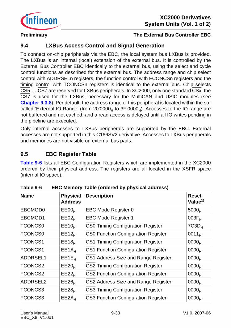
XC2000 DerivativesSystem Units (Vol. 1 of 2)
The External Bus Controller EBCPreliminary
9.4 LXBus Access Control and Signal GenerationTo connect on-chip peripherals via the EBC, the local system bus LXBus is provided.The LXBus is an internal (local) extension of the external bus. It is controlled by theExternal Bus Controller EBC identically to the external bus, using the select and cyclecontrol functions as described for the external bus. The address range and chip selectcontrol with ADDRSELn registers, the function control with FCONCSn registers and thetiming control with TCONCSn registers is identical to the external bus. Chip selectsCS5 … CS7 are reserved for LXBus peripherals. In XC2000, only one standard CSx, theCS7 is used for the LXBus, necessary for the MultiCAN and USIC modules (seeChapter 9.3.8). Per default, the address range of this peripheral is located within the so-called ‘External IO Range’ (from 20’0000H to 3F’0000H). Accesses to the IO range arenot buffered and not cached, and a read access is delayed until all IO writes pending inthe pipeline are executed.Only internal accesses to LXBus peripherals are supported by the EBC. Externalaccesses are not supported in this C166SV2 derivative. Accesses to LXBus peripheralsand memories are not visible on external bus pads.
9.5 EBC Register TableTable 9-6 lists all EBC Configuration Registers which are implemented in the XC2000ordered by their physical address. The registers are all located in the XSFR space(internal IO space).
Table 9-6 EBC Memory Table (ordered by physical address)Name Physical
AddressDescription Reset
Value1)
EBCMOD0 EE00H EBC Mode Register 0 5000H
EBCMOD1 EE02H EBC Mode Register 1 003FH
TCONCS0 EE10H CS0 Timing Configuration Register 7C3DH
FCONCS0 EE12H CS0 Function Configuration Register 0011H
TCONCS1 EE18H CS1 Timing Configuration Register 0000H
FCONCS1 EE1AH CS1 Function Configuration Register 0000H
ADDRSEL1 EE1EH CS1 Address Size and Range Register 0000H
TCONCS2 EE20H CS2 Timing Configuration Register 0000H
FCONCS2 EE22H CS2 Function Configuration Register 0000H
ADDRSEL2 EE26H CS2 Address Size and Range Register 0000H
TCONCS3 EE28H CS3 Timing Configuration Register 0000H
FCONCS3 EE2AH CS3 Function Configuration Register 0000H
User’s Manual 9-33 V1.0, 2007-06EBC_X8, V1.0d1
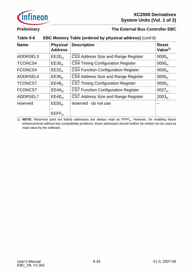
XC2000 DerivativesSystem Units (Vol. 1 of 2)
The External Bus Controller EBCPreliminary
ADDRSEL3 EE2EH CS3 Address Size and Range Register 0000H
TCONCS4 EE30H CS4 Timing Configuration Register 0000H
FCONCS4 EE32H CS4 Function Configuration Register 0000H
ADDRSEL4 EE36H CS4 Address Size and Range Register 0000H
TCONCS7 EE48H CS7 Timing Configuration Register 0000H
FCONCS7 EE4AH CS7 Function Configuration Register 0027H
ADDRSEL7 EE4EH CS7 Address Size and Range Register 2003H
reserved EE50H-EEFFH
reserved - do not use –
1) NOTE: Reserved (and not listed) addresses are always read as FFFFH. However, for enabling futureenhancements without any compatibility problems, these addresses should neither be written nor be used asread value by the software.
Table 9-6 EBC Memory Table (ordered by physical address) (cont’d)
Name Physical Address
Description Reset Value1)
User’s Manual 9-34 V1.0, 2007-06EBC_X8, V1.0d1
XC2000 DerivativesSystem Units (Vol. 1 of 2)
Startup Configuration and Bootstrap LoadingPreliminary
10 Startup Configuration and Bootstrap LoadingAfter start-up, the XC2000 executes code out of an on-chip or off-chip program memory. The initial code source can be selected via hardware configuration (i.e. defined levels on specific pins):• Internal Start Mode: executes code out of the on-chip program Flash.• External Start Mode: executes code out of an off-chip memory connected to the
External Bus Interface.• Bootstrap Loading Modes: execute code out of the on-chip program SRAM
(PSRAM). This code is downloaded beforehand via a selectable serial interface.
10.1 Start-Up Mode SelectionAfter any device start-up the currently valid start-up configuration is indicated in bitfield HWCFG of register SCU_STSTAT. Table 10-1 summarizes the defined start up modes.A start-up configuration can be selected in two ways:• Via an externally applied hardware configuration upon a Power-on or Internal
Application reset The hardware configuration is applied to Port 10 pins (P10.[3:0]). The hardware that activates a startup configuration during reset may be simple pull resistors for systems that use this feature upon every reset. You may want to use a switchable solution (via jumpers or an external signal) for systems that only temporarily use a hardware configuration.
• By executing the following software sequence (using register SCU_SWRSTCON, described in Section 6.2.10.2):– Write respective configuration value (refer to Table 10-1) to bitfield SWCFG;– Set Software Boot Configuration bit: SWBOOT = 1;– Trigger a software reset by activating Software Reset Request: SWRSTREQ = 1.
Note: After an Application reset the hardware configuration from P10 will not be evaluated, but the same configuration will be used as upon the previous reset.
User’s Manual 10-1 V1.0, 2007-06SCFG/BSL, V1.0
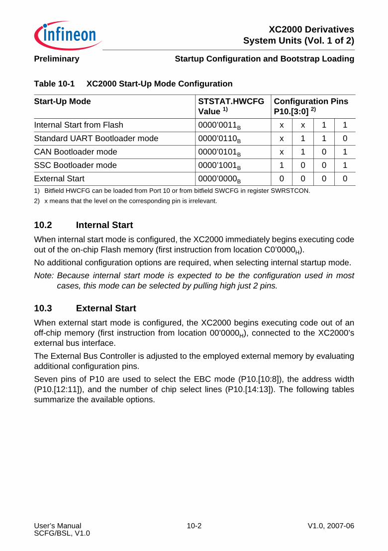
XC2000 DerivativesSystem Units (Vol. 1 of 2)
Startup Configuration and Bootstrap LoadingPreliminary
10.2 Internal StartWhen internal start mode is configured, the XC2000 immediately begins executing code out of the on-chip Flash memory (first instruction from location C0’0000H).No additional configuration options are required, when selecting internal startup mode.Note: Because internal start mode is expected to be the configuration used in most
cases, this mode can be selected by pulling high just 2 pins.
10.3 External StartWhen external start mode is configured, the XC2000 begins executing code out of an off-chip memory (first instruction from location 00’0000H), connected to the XC2000’s external bus interface.The External Bus Controller is adjusted to the employed external memory by evaluating additional configuration pins.Seven pins of P10 are used to select the EBC mode (P10.[10:8]), the address width (P10.[12:11]), and the number of chip select lines (P10.[14:13]). The following tables summarize the available options.
Table 10-1 XC2000 Start-Up Mode Configuration
Start-Up Mode STSTAT.HWCFG Value 1)
1) Bitfield HWCFG can be loaded from Port 10 or from bitfield SWCFG in register SWRSTCON.
Configuration Pins P10.[3:0] 2)
2) x means that the level on the corresponding pin is irrelevant.
Internal Start from Flash 0000’0011B x x 1 1Standard UART Bootloader mode 0000’0110B x 1 1 0CAN Bootloader mode 0000’0101B x 1 0 1SSC Bootloader mode 0000’1001B 1 0 0 1External Start 0000’0000B 0 0 0 0
User’s Manual 10-2 V1.0, 2007-06SCFG/BSL, V1.0
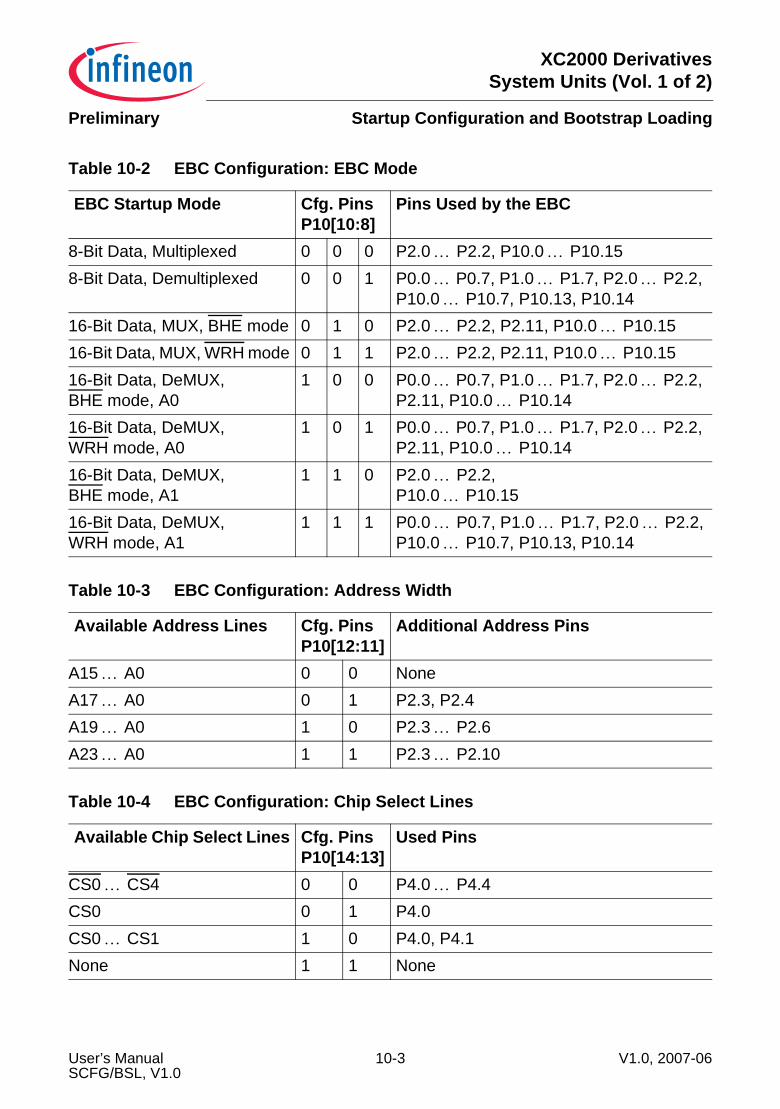
XC2000 DerivativesSystem Units (Vol. 1 of 2)
Startup Configuration and Bootstrap LoadingPreliminary
Table 10-2 EBC Configuration: EBC Mode
EBC Startup Mode Cfg. Pins P10[10:8]
Pins Used by the EBC
8-Bit Data, Multiplexed 0 0 0 P2.0 … P2.2, P10.0 … P10.158-Bit Data, Demultiplexed 0 0 1 P0.0 … P0.7, P1.0 … P1.7, P2.0 … P2.2,
P10.0 … P10.7, P10.13, P10.1416-Bit Data, MUX, BHE mode 0 1 0 P2.0 … P2.2, P2.11, P10.0 … P10.1516-Bit Data, MUX, WRH mode 0 1 1 P2.0 … P2.2, P2.11, P10.0 … P10.1516-Bit Data, DeMUX, BHE mode, A0
1 0 0 P0.0 … P0.7, P1.0 … P1.7, P2.0 … P2.2, P2.11, P10.0 … P10.14
16-Bit Data, DeMUX, WRH mode, A0
1 0 1 P0.0 … P0.7, P1.0 … P1.7, P2.0 … P2.2, P2.11, P10.0 … P10.14
16-Bit Data, DeMUX, BHE mode, A1
1 1 0 P2.0 … P2.2, P10.0 … P10.15
16-Bit Data, DeMUX, WRH mode, A1
1 1 1 P0.0 … P0.7, P1.0 … P1.7, P2.0 … P2.2, P10.0 … P10.7, P10.13, P10.14
Table 10-3 EBC Configuration: Address Width
Available Address Lines Cfg. Pins P10[12:11]
Additional Address Pins
A15 … A0 0 0 NoneA17 … A0 0 1 P2.3, P2.4A19 … A0 1 0 P2.3 … P2.6A23 … A0 1 1 P2.3 … P2.10
Table 10-4 EBC Configuration: Chip Select Lines
Available Chip Select Lines Cfg. Pins P10[14:13]
Used Pins
CS0 … CS4 0 0 P4.0 … P4.4CS0 0 1 P4.0CS0 … CS1 1 0 P4.0, P4.1None 1 1 None
User’s Manual 10-3 V1.0, 2007-06SCFG/BSL, V1.0
XC2000 DerivativesSystem Units (Vol. 1 of 2)
Startup Configuration and Bootstrap LoadingPreliminary
10.4 Bootstrap Loading Bootstrap Loading is the technique of transferring code to the XC2000 via a certain interface (usually serial) before the regular code execution out of non-volatile program memory commences. Instead, the XC2000 executes the previously received code.This boot-code may be complete (e.g. temporary software for testing or calibration), amend existing code in non-volatile program memory (e.g. with product-specific data or routines), or load additional code (e.g. using higher or more secure protocols). A possible application for bootstrap loading is the programming of virgin Flash memory at the end of a production line, with no external memory or internal Flash required for the initialization code.The BSL mechanism may be used for standard system startup as well as only for special occasions like system maintenance (firmware update) or end-of-line programming or testing.The XC2000 supports bootstrap loading using several protocols/modes:• Standard UART protocol, loading 32 bytes (see Section 10.4.2)• Synchronous serial protocol (see Section 10.4.3)• CAN protocol (see Section 10.4.4)For a summary of these modes, see also Table 10-10
10.4.1 General FunctionalityEven though each bootstrap loader has its particular functionality, the general handling is the same for all of them.
Entering a Bootstrap LoaderBootstrap loaders are enabled by selecting a specific start-up configuration (see Section 10.1).The required configuration patterns are described in Table 10-10 for the bootstrap loaders, and are summarized in Table 10-1.
User’s Manual 10-4 V1.0, 2007-06SCFG/BSL, V1.0
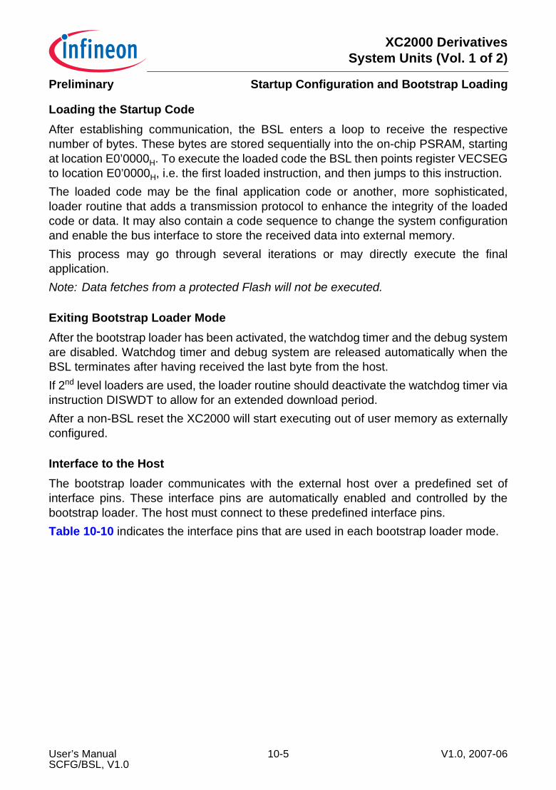
XC2000 DerivativesSystem Units (Vol. 1 of 2)
Startup Configuration and Bootstrap LoadingPreliminary
Loading the Startup CodeAfter establishing communication, the BSL enters a loop to receive the respective number of bytes. These bytes are stored sequentially into the on-chip PSRAM, starting at location E0’0000H. To execute the loaded code the BSL then points register VECSEG to location E0’0000H, i.e. the first loaded instruction, and then jumps to this instruction.The loaded code may be the final application code or another, more sophisticated, loader routine that adds a transmission protocol to enhance the integrity of the loaded code or data. It may also contain a code sequence to change the system configuration and enable the bus interface to store the received data into external memory.This process may go through several iterations or may directly execute the final application.Note: Data fetches from a protected Flash will not be executed.
Exiting Bootstrap Loader ModeAfter the bootstrap loader has been activated, the watchdog timer and the debug system are disabled. Watchdog timer and debug system are released automatically when the BSL terminates after having received the last byte from the host.If 2nd level loaders are used, the loader routine should deactivate the watchdog timer via instruction DISWDT to allow for an extended download period.After a non-BSL reset the XC2000 will start executing out of user memory as externally configured.
Interface to the HostThe bootstrap loader communicates with the external host over a predefined set of interface pins. These interface pins are automatically enabled and controlled by the bootstrap loader. The host must connect to these predefined interface pins.Table 10-10 indicates the interface pins that are used in each bootstrap loader mode.
User’s Manual 10-5 V1.0, 2007-06SCFG/BSL, V1.0
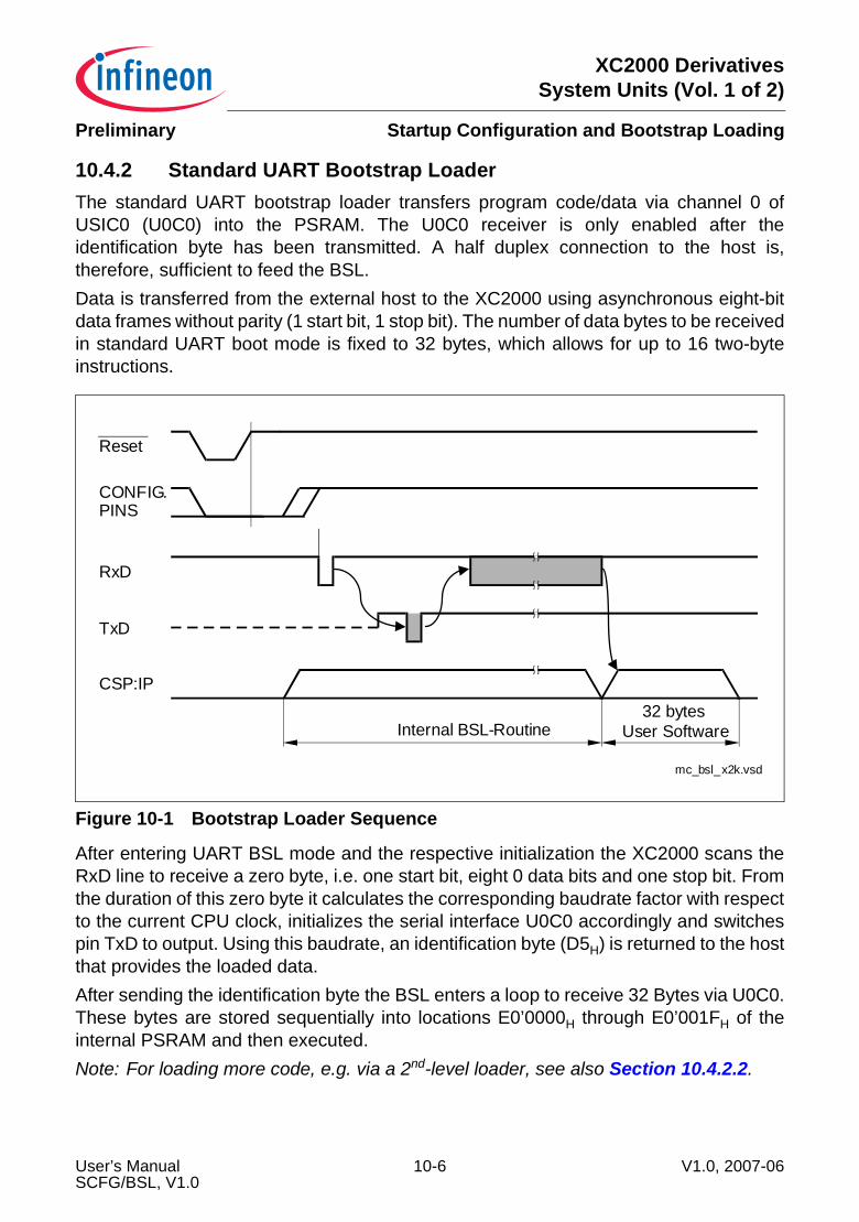
XC2000 DerivativesSystem Units (Vol. 1 of 2)
Startup Configuration and Bootstrap LoadingPreliminary
10.4.2 Standard UART Bootstrap LoaderThe standard UART bootstrap loader transfers program code/data via channel 0 of USIC0 (U0C0) into the PSRAM. The U0C0 receiver is only enabled after the identification byte has been transmitted. A half duplex connection to the host is, therefore, sufficient to feed the BSL.Data is transferred from the external host to the XC2000 using asynchronous eight-bit data frames without parity (1 start bit, 1 stop bit). The number of data bytes to be received in standard UART boot mode is fixed to 32 bytes, which allows for up to 16 two-byteinstructions.
Figure 10-1 Bootstrap Loader Sequence
After entering UART BSL mode and the respective initialization the XC2000 scans the RxD line to receive a zero byte, i.e. one start bit, eight 0 data bits and one stop bit. From the duration of this zero byte it calculates the corresponding baudrate factor with respect to the current CPU clock, initializes the serial interface U0C0 accordingly and switches pin TxD to output. Using this baudrate, an identification byte (D5H) is returned to the host that provides the loaded data.After sending the identification byte the BSL enters a loop to receive 32 Bytes via U0C0. These bytes are stored sequentially into locations E0’0000H through E0’001FH of the internal PSRAM and then executed.Note: For loading more code, e.g. via a 2nd-level loader, see also Section 10.4.2.2.
mc_bsl_x2k.vsd
Reset
CONFIG. PINS
RxD
TxD
CSP:IP32 bytes
User SoftwareInternal BSL-Routine
User’s Manual 10-6 V1.0, 2007-06SCFG/BSL, V1.0
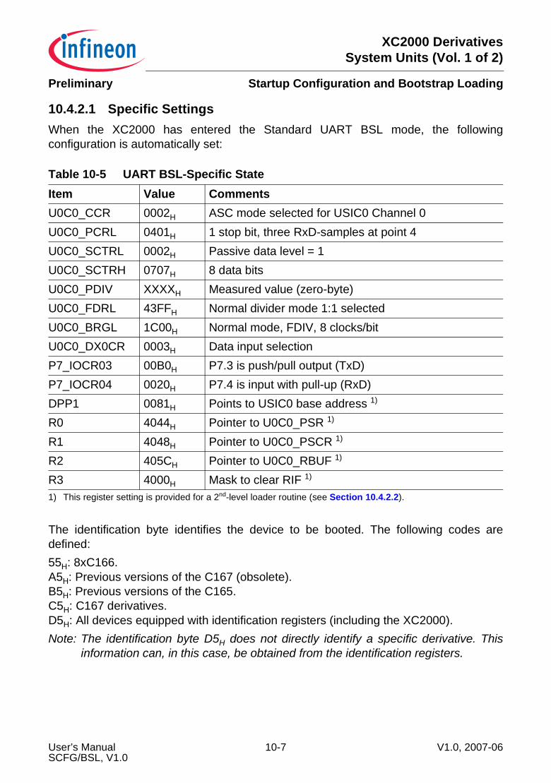
XC2000 DerivativesSystem Units (Vol. 1 of 2)
Startup Configuration and Bootstrap LoadingPreliminary
10.4.2.1 Specific SettingsWhen the XC2000 has entered the Standard UART BSL mode, the following configuration is automatically set:
The identification byte identifies the device to be booted. The following codes are defined:55H: 8xC166. A5H: Previous versions of the C167 (obsolete). B5H: Previous versions of the C165. C5H: C167 derivatives. D5H: All devices equipped with identification registers (including the XC2000).Note: The identification byte D5H does not directly identify a specific derivative. This
information can, in this case, be obtained from the identification registers.
Table 10-5 UART BSL-Specific StateItem Value CommentsU0C0_CCR 0002H ASC mode selected for USIC0 Channel 0U0C0_PCRL 0401H 1 stop bit, three RxD-samples at point 4U0C0_SCTRL 0002H Passive data level = 1U0C0_SCTRH 0707H 8 data bitsU0C0_PDIV XXXXH Measured value (zero-byte)U0C0_FDRL 43FFH Normal divider mode 1:1 selectedU0C0_BRGL 1C00H Normal mode, FDIV, 8 clocks/bitU0C0_DX0CR 0003H Data input selectionP7_IOCR03 00B0H P7.3 is push/pull output (TxD)P7_IOCR04 0020H P7.4 is input with pull-up (RxD)DPP1 0081H Points to USIC0 base address 1)
1) This register setting is provided for a 2nd-level loader routine (see Section 10.4.2.2).
R0 4044H Pointer to U0C0_PSR 1)
R1 4048H Pointer to U0C0_PSCR 1)
R2 405CH Pointer to U0C0_RBUF 1)
R3 4000H Mask to clear RIF 1)
User’s Manual 10-7 V1.0, 2007-06SCFG/BSL, V1.0
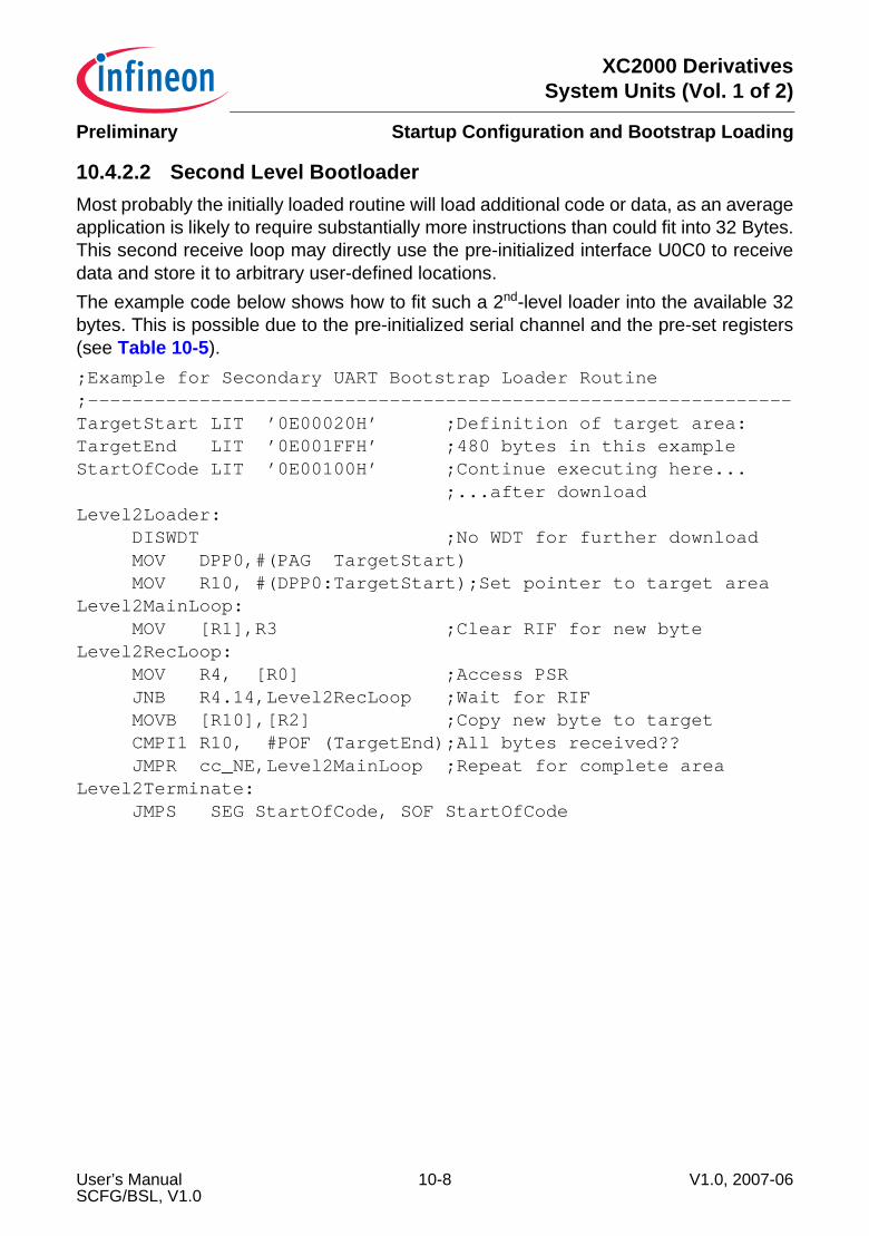
XC2000 DerivativesSystem Units (Vol. 1 of 2)
Startup Configuration and Bootstrap LoadingPreliminary
10.4.2.2 Second Level BootloaderMost probably the initially loaded routine will load additional code or data, as an average application is likely to require substantially more instructions than could fit into 32 Bytes. This second receive loop may directly use the pre-initialized interface U0C0 to receive data and store it to arbitrary user-defined locations.The example code below shows how to fit such a 2nd-level loader into the available 32 bytes. This is possible due to the pre-initialized serial channel and the pre-set registers (see Table 10-5).;Example for Secondary UART Bootstrap Loader Routine;---------------------------------------------------------------TargetStart LIT ’0E00020H’ ;Definition of target area:TargetEnd LIT ’0E001FFH’ ;480 bytes in this exampleStartOfCode LIT ’0E00100H’ ;Continue executing here... ;...after downloadLevel2Loader: DISWDT ;No WDT for further download MOV DPP0,#(PAG TargetStart) MOV R10, #(DPP0:TargetStart);Set pointer to target areaLevel2MainLoop: MOV [R1],R3 ;Clear RIF for new byteLevel2RecLoop: MOV R4, [R0] ;Access PSR JNB R4.14,Level2RecLoop ;Wait for RIF MOVB [R10],[R2] ;Copy new byte to target CMPI1 R10, #POF (TargetEnd);All bytes received?? JMPR cc_NE,Level2MainLoop ;Repeat for complete areaLevel2Terminate: JMPS SEG StartOfCode, SOF StartOfCode
User’s Manual 10-8 V1.0, 2007-06SCFG/BSL, V1.0
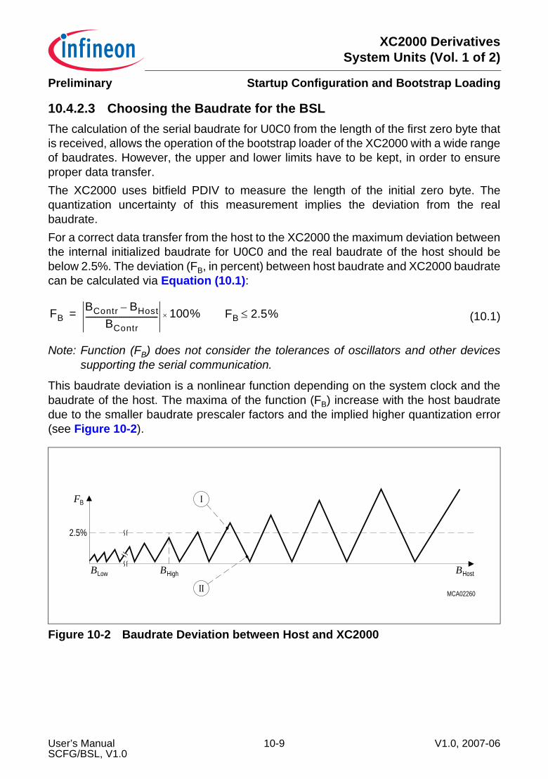
XC2000 DerivativesSystem Units (Vol. 1 of 2)
Startup Configuration and Bootstrap LoadingPreliminary
10.4.2.3 Choosing the Baudrate for the BSL The calculation of the serial baudrate for U0C0 from the length of the first zero byte that is received, allows the operation of the bootstrap loader of the XC2000 with a wide range of baudrates. However, the upper and lower limits have to be kept, in order to ensure proper data transfer.The XC2000 uses bitfield PDIV to measure the length of the initial zero byte. The quantization uncertainty of this measurement implies the deviation from the real baudrate.For a correct data transfer from the host to the XC2000 the maximum deviation between the internal initialized baudrate for U0C0 and the real baudrate of the host should be below 2.5%. The deviation (FB, in percent) between host baudrate and XC2000 baudrate can be calculated via Equation (10.1):
(10.1)
Note: Function (FB) does not consider the tolerances of oscillators and other devices supporting the serial communication.
This baudrate deviation is a nonlinear function depending on the system clock and the baudrate of the host. The maxima of the function (FB) increase with the host baudrate due to the smaller baudrate prescaler factors and the implied higher quantization error (see Figure 10-2).
Figure 10-2 Baudrate Deviation between Host and XC2000
FBBContr BHost–
BContr------------------------------------- 100%×= FB 2.5%≤
MCA02260
BF
2.5%
LowB BHigh
Ι
ΙΙ
BHost
User’s Manual 10-9 V1.0, 2007-06SCFG/BSL, V1.0
XC2000 DerivativesSystem Units (Vol. 1 of 2)
Startup Configuration and Bootstrap LoadingPreliminary
The minimum baudrate (BLow in Figure 10-2) is determined by the maximum count capacity of bitfield PDIV, when measuring the zero byte, i.e. it depends on the system clock. The minimum baudrate is obtained by using the maximum PDIV count 210 in the baudrate formula. Baudrates below BLow would cause PDIV to overflow. In this case U0C0 cannot be initialized properly and the communication with the external host is likely to fail.The maximum baudrate (BHigh in Figure 10-2) is the highest baudrate where the deviation still does not exceed the limit, i.e. all baudrates between BLow and BHigh are below the deviation limit. BHigh marks the baudrate up to which communication with the external host will work properly without additional tests or investigations.Higher baudrates, however, may be used as long as the actual deviation does not exceed the indicated limit. A certain baudrate (marked I) in Figure 10-2) may e.g. violate the deviation limit, while an even higher baudrate (marked II) in Figure 10-2) stays very well below it. Any baudrate can be used for the bootstrap loader provided that the following three prerequisites are fulfilled:• the baudrate is within the specified operating range for U0C0• the external host is able to use this baudrate• the computed deviation error is below the limit.Note: When the bootstrap loader mode is entered after a power reset, the bootstrap
loader will begin to operate with fSYS = fIOSC × 2 (approximately 10 MHz) which will limit the maximum baudrate for U0C0. Higher levels of the bootstrapping sequence can then switch the clock generation mode in order to achieve higher baudrates for the download.
User’s Manual 10-10 V1.0, 2007-06SCFG/BSL, V1.0
XC2000 DerivativesSystem Units (Vol. 1 of 2)
Startup Configuration and Bootstrap LoadingPreliminary
10.4.3 Synchronous Serial Channel Bootstrap LoaderThe Synchronous Serial Channel (SSC) bootstrap loader transfers program code/data from an external serial EEPROM via channel 0 of USIC0 (U0C0) into the PSRAM. The XC2000 is the master, so no additional elements (except for the EEPROM) are required.Data is transferred from the external EEPROM to the XC2000 using synchronous eight-bit data frames with MSB first. The number of data bytes to be received in SSC boot mode is user-selectable. The serial clock rate is set to fSYS/10, which results in 1 MHz after a power reset.After entering SSC BSL mode and the respective initialization, the XC2000 first reads the header from the first addresses (00...0) of the target EEPROM. This header consists of two items:• The memory identification Byte: D5H• The data size field: 1 byte or 2 bytes, depending on the EEPROM’s addressing mode
(8-bit or 16-bit, see Section 10.4.3.1)If both items are valid the BSL enters a loop to read the number of bytes defined by the data size field (maximum is FFH or FF00H, depending on the EEPROM) via U0C0.These bytes are stored sequentially into PSRAM starting at location E0’0000H and are then executed. Therefore, the size of the PSRAM in the respective derivative determines the real maximum block size to be downloaded.An invalid header (identification byte ≠ D5H, data size field = 0 or greater than 65280/FF00H) is indicated by toggling the CS line low 3 times. This helps debugging during the system setup phase.
User’s Manual 10-11 V1.0, 2007-06SCFG/BSL, V1.0
XC2000 DerivativesSystem Units (Vol. 1 of 2)
Startup Configuration and Bootstrap LoadingPreliminary
10.4.3.1 Supported EEPROM TypesThe XC2000’s SSC bootstrap loader assumes an SPI-compatible EEPROM (25xxx series). It supports devices with 8-bit addressing as well as with 16-bit addressing. The connected EEPROM type is determined by examining the received header bytes, as indicated in Table 10-6.
Note: The value of the returned default bytes (indicated as XXH) depends on the employed EEPROM type.
Table 10-6 Determining the EEPROM TypeSSC Frame Number
Meaning of Transmitted Data
Received Data from 8-bit Addr. Device
Received Data from 16-bit Addr. Device
1 03H: Read command XXH (default level) XXH (default level)2 00H: Address byte
(high for 16-bit addr.)XXH (default level) XXH (default level)
3 00H: Address byte low Identification Byte XXH (default level)4 00H: Dummy byte Size field Identification Byte5 00H: Dummy byte Data byte 1 Size field, high Byte6 00H: Dummy byte Data byte 2 Size field, low Byte7 00H: Dummy byte Data byte 3 Data byte 1… 00H: Dummy byte Data byte 4 … n Data byte 2 … n
User’s Manual 10-12 V1.0, 2007-06SCFG/BSL, V1.0

XC2000 DerivativesSystem Units (Vol. 1 of 2)
Startup Configuration and Bootstrap LoadingPreliminary
10.4.3.2 Specific SettingsWhen the XC2000 has entered the SSC BSL mode, the following configuration is automatically set:
Table 10-7 SSC BSL-Specific StateItem Value CommentsU0C0_CCR 0001H SSC mode selected for USIC0 Channel 0U0C0_PCRL 0011H SSC master mode, frequency from fPPP U0C0_PCRH 8000H MCLK generation is enabledU0C0_SCTRL 0103H MSB first, passive data level=1U0C0_SCTRH 073FH 8 data bits, infinite frameU0C0_DX0CR 0015H Data input selectionU0C0_FDRL 43FFH Normal divider mode 1:1 selectedU0C0_BRGL 0000H Normal mode, FDIV - default value after resetU0C0_BRGH 8004H Passive levels MCLK/SCLK=0, PDIV=4P2_IOCR03 00D0H P2.3 is open-drain output (MTSR)P2_IOCR04 0020H P2.4 is input with pull-up (MRST)P2_IOCR05 00D0H P2.5 is open-drain output (SCLK)P2_IOCR06 00C0H P2.6 is open-drain output (SLS)
User’s Manual 10-13 V1.0, 2007-06SCFG/BSL, V1.0
XC2000 DerivativesSystem Units (Vol. 1 of 2)
Startup Configuration and Bootstrap LoadingPreliminary
10.4.4 CAN Bootstrap LoaderThe CAN bootstrap loader transfers program code/data via node 0 of the MultiCAN module into the PSRAM. Data is transferred from the external host to the XC2000 using eight-byte data frames. The number of data frames to be received is programmable and determined by the 16-bit data message count value DMSGC.The communication between XC2000 and external host is based on the following three CAN standard frames:• Initialization frame - sent by the external host to the XC2000• Acknowledge frame - sent by the XC2000 to the external host• Data frame(s) - sent by the external host to the XC2000The initialization frame is used in the XC2000 for baud rate detection. After a successful baud rate detection is reported to the external host by sending the acknowledge frame, data is transmitted using data frames. Table 10-8 shows the parameters and settings forthe three utilized CAN standard frames.Note: The CAN bootstrap loader requires a point-to-point connection with the host, i.e.
the XC2000 must be only CAN node connected to the network. A crystal with at least 4 MHz is required for CAN bootstrap loader operation.
Initialization PhaseThe first task is to determine the CAN baud rate at which the external host is communicating. This task requires the external host to send initialization frames continuously to the XC2000. The first two data bytes of the initialization frame include a 2-byte baud rate detection pattern (5555H), an 11-bit (2-byte) identifier ACKID1) for the acknowledge frame, a 16-bit data message count value DMSGC, and an 11-bit (2-byte) identifier DMSGID1) to be used by the data frame(s).The CAN baud rate is determined by analyzing the received baud rate detection pattern (5555H) and the baud rate registers of the MultiCAN module are set accordingly. The XC2000 is now ready to receive CAN frames with the baud rate of the external host.
Acknowledge PhaseIn the acknowledge phase, the bootstrap loader waits until it receives the next correctly recognized initialization frame from the external host, and acknowledges this frame by generating a dominant bit in its ACK slot. Afterwards, the bootstrap loader transmits an acknowledge frame back to the external host, indicating that it is now ready to receive data frames. The acknowledge frame uses the message identifier ACKID that has been received with the initialization frame.
1) The CAN bootstrap loader copies the two identifier bytes received in the initialization frame directly to register MOAR. Therefore, the respective fields in the initialization frame must contain the intended identifier padded with two dummy bits at the lower end and extended with bitfields IDE (=0B) and PRI (=01B) at the upper end.
User’s Manual 10-14 V1.0, 2007-06SCFG/BSL, V1.0
XC2000 DerivativesSystem Units (Vol. 1 of 2)
Startup Configuration and Bootstrap LoadingPreliminary
Data Transmission PhaseIn the data transmission phase, data frames are sent by the external host and received by the XC2000. The data frames use the 11-bit data message identifier DMSGID that has been sent with the initialization frame. Eight data bytes are transmitted with each data frame. The first data byte is stored in PSRAM at E0’0000H. Consecutive data bytes are stored at incrementing addresses.Both communication partners evaluate the data message count DMSGC until the requested number of CAN data frames has been transmitted. After the reception of the last CAN data frame, the bootstrap loader finishes and executes the loaded code.
Timing ParametersThere are no general restrictions for CAN timings of the external host. During the initialization phase the external host transmits initialization frames. If no acknowledge frame is sent back within a certain time as defined in the external host (e.g. after a dedicated number of initialization frame transmissions), the external host can decide that the XC2000 is not able to establish the CAN boot communication link.
Table 10-8 CAN Bootstrap Loader Frames Frame Type Parameter DescriptionInitialization Frame
Identifier 11-bit, don’t careDLC = 8 Data length code, 8 bytes within CAN frameData bytes 0/1 Baud rate detection pattern (5555H)Data bytes 2/3 Acknowledge message identifier ACKID
(complete register contents)Data bytes 4/5 Data message count DMSGC, 16-bitData bytes 6/7 Data message identifier DMSGID
(complete register contents)Acknowledge Frame
Identifier Acknowledge message identifier ACKID as received by data bytes [3:2] of the initialization frame
DLC = 4 Data length code, 4 bytes within CAN frameData bytes 0/1 Contents of bit-timing registerData bytes 2/3 Copy of acknowledge identifier from initialization frame
Data frame Identifier Data message identifier DMSGID as sent by data bytes [7:6] of the initialization frame
DLC = 8 Data length code, 8 bytes within CAN frameData bytes 0 to 7
Data bytes, assigned to increasing destination (PSRAM) addresses
User’s Manual 10-15 V1.0, 2007-06SCFG/BSL, V1.0
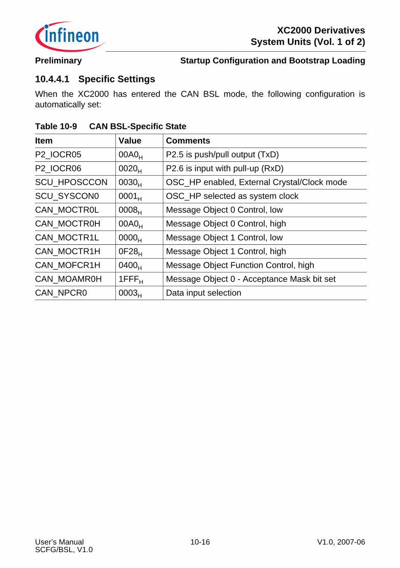
XC2000 DerivativesSystem Units (Vol. 1 of 2)
Startup Configuration and Bootstrap LoadingPreliminary
10.4.4.1 Specific SettingsWhen the XC2000 has entered the CAN BSL mode, the following configuration is automatically set:
Table 10-9 CAN BSL-Specific StateItem Value CommentsP2_IOCR05 00A0H P2.5 is push/pull output (TxD)P2_IOCR06 0020H P2.6 is input with pull-up (RxD)SCU_HPOSCCON 0030H OSC_HP enabled, External Crystal/Clock modeSCU_SYSCON0 0001H OSC_HP selected as system clockCAN_MOCTR0L 0008H Message Object 0 Control, low CAN_MOCTR0H 00A0H Message Object 0 Control, high CAN_MOCTR1L 0000H Message Object 1 Control, low CAN_MOCTR1H 0F28H Message Object 1 Control, high CAN_MOFCR1H 0400H Message Object Function Control, high CAN_MOAMR0H 1FFFH Message Object 0 - Acceptance Mask bit set CAN_NPCR0 0003H Data input selection
User’s Manual 10-16 V1.0, 2007-06SCFG/BSL, V1.0
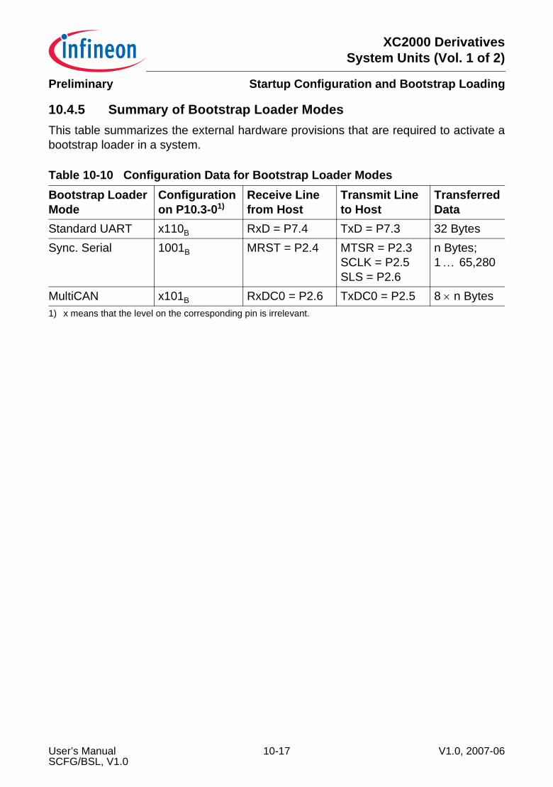
XC2000 DerivativesSystem Units (Vol. 1 of 2)
Startup Configuration and Bootstrap LoadingPreliminary
10.4.5 Summary of Bootstrap Loader ModesThis table summarizes the external hardware provisions that are required to activate a bootstrap loader in a system.
Table 10-10 Configuration Data for Bootstrap Loader ModesBootstrap Loader Mode
Configuration on P10.3-01)
1) x means that the level on the corresponding pin is irrelevant.
Receive Line from Host
Transmit Line to Host
Transferred Data
Standard UART x110B RxD = P7.4 TxD = P7.3 32 BytesSync. Serial 1001B MRST = P2.4 MTSR = P2.3
SCLK = P2.5SLS = P2.6
n Bytes; 1 … 65,280
MultiCAN x101B RxDC0 = P2.6 TxDC0 = P2.5 8 × n Bytes
User’s Manual 10-17 V1.0, 2007-06SCFG/BSL, V1.0
XC2000 DerivativesSystem Units (Vol. 1 of 2)
Startup Configuration and Bootstrap LoadingPreliminary
User’s Manual 10-18 V1.0, 2007-06SCFG/BSL, V1.0
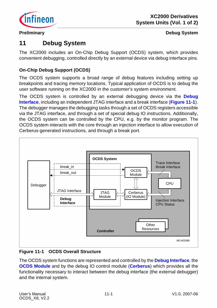
XC2000 DerivativesSystem Units (Vol. 1 of 2)
Debug SystemPreliminary
11 Debug SystemThe XC2000 includes an On-Chip Debug Support (OCDS) system, which providesconvenient debugging, controlled directly by an external device via debug interface pins.
On-Chip Debug Support (OCDS)The OCDS system supports a broad range of debug features including setting upbreakpoints and tracing memory locations. Typical application of OCDS is to debug theuser software running on the XC2000 in the customer’s system environment.The OCDS system is controlled by an external debugging device via the DebugInterface, including an independent JTAG interface and a break interface (Figure 11-1).The debugger manages the debugging tasks through a set of OCDS registers accessiblevia the JTAG interface, and through a set of special debug IO instructions. Additionally,the OCDS system can be controlled by the CPU, e.g. by the monitor program. TheOCDS system interacts with the core through an injection interface to allow execution ofCerberus-generated instructions, and through a break port.
Figure 11-1 OCDS Overall Structure
The OCDS system functions are represented and controlled by the Debug Interface, theOCDS Module and by the debug IO control module (Cerberus) which provides all thefunctionality necessary to interact between the debug interface (the external debugger)and the internal system.
Controller
OCDS System
Debugger
MCA05388
JTAG Interface JTAGModule
Cerberus(IO Module)Debug
Interface
OCDSModule
OtherResources
Trace InterfaceBreak Interface
Injection InterfaceCPU Status
CPU
break_inbreak_out
User’s Manual 11-1 V1.0, 2007-06OCDS_X8, V2.2
XC2000 DerivativesSystem Units (Vol. 1 of 2)
Debug SystemPreliminary
The OCDS system provides the following basic features:• Hardware, software and external pin breakpoints• Reaction on break with CPU-Halt, monitor call, data transfer and external signal• Read/write access to the whole address space• Single stepping• Debug Interface pins for JTAG interface and break interface• Injection of arbitrary instructions• Fast memory tracing through transfer to external bus• Analysis and status registers
11.1 Debug InterfaceThe Debug Interface is a channel to access XC2000 On-Chip Debug Support (OCDS)resources. Through it data can be transferred to/from all on- and off-chip (if any)memories and control registers.
Features and Functions• Independent interface for On-Chip Debug Support (OCDS)• JTAG port based on the IEEE 1149 JTAG standard• Break interface for external trigger and indication of breaks• Generic memory access functionality• Independent data transfer channel for e.g. programming of on-chip non volatile
memoryThe Debug Interface is represented by:• Standard JTAG Interface• Two additional XC2000 specific signals - OCDS Break-Interface
JTAG InterfaceThe JTAG interface is a standardized and dedicated port usually used for boundary scanand for chip internal tests. Because both of these applications are not enabled duringnormal operation of the device in a system, the JTAG port is an ideal interface fordebugging tasks.This interface holds the JTAG IEEE.1149-standard signals:• TDI - Serial data input• TDO - Serial data output• TCK - JTAG clock• TMS - State machine control signal• TRST - Reset/Module enable
User’s Manual 11-2 V1.0, 2007-06OCDS_X8, V2.2
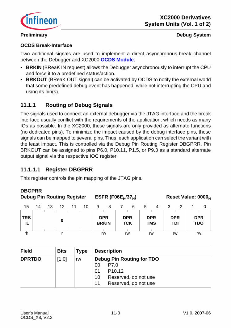
XC2000 DerivativesSystem Units (Vol. 1 of 2)
Debug SystemPreliminary
OCDS Break-InterfaceTwo additional signals are used to implement a direct asynchronous-break channelbetween the Debugger and XC2000 OCDS Module:• BRKIN (BReaK IN request) allows the Debugger asynchronously to interrupt the CPU
and force it to a predefined status/action.• BRKOUT (BReaK OUT signal) can be activated by OCDS to notify the external world
that some predefined debug event has happened, while not interrupting the CPU andusing its pin(s).
11.1.1 Routing of Debug SignalsThe signals used to connect an external debugger via the JTAG interface and the breakinterface usually conflict with the requirements of the application, which needs as manyIOs as possible. In the XC2000, these signals are only provided as alternate functions(no dedicated pins). To minimize the impact caused by the debug interface pins, thesesignals can be mapped to several pins. Thus, each application can select the variant withthe least impact. This is controlled via the Debug Pin Routing Register DBGPRR. PinBRKOUT can be assigned to pins P6.0, P10.11, P1.5, or P9.3 as a standard alternateoutput signal via the respective IOC register.
11.1.1.1 Register DBGPRRThis register controls the pin mapping of the JTAG pins.
DBGPRRDebug Pin Routing Register ESFR (F06EH/37H) Reset Value: 0000H
15 14 13 12 11 10 9 8 7 6 5 4 3 2 1 0
TRSTL 0 DPR
BRKINDPRTCK
DPRTMS
DPRTDI
DPRTDO
rh r rw rw rw rw rw
Field Bits Type DescriptionDPRTDO [1:0] rw Debug Pin Routing for TDO
00 P7.001 P10.1210 Reserved, do not use11 Reserved, do not use
User’s Manual 11-3 V1.0, 2007-06OCDS_X8, V2.2
XC2000 DerivativesSystem Units (Vol. 1 of 2)
Debug SystemPreliminary
DPRTDI [3:2] rw Debug Pin Routing for TDI00 P5.201 P10.1010 P7.211 P8.3
DPRTMS [5:4] rw Debug Pin Routing for TMS00 P5.401 P10.1110 P7.311 P8.4
DPRTCK [7:6] rw Debug Pin Routing for TCK00 P2.901 P10.910 P7.411 P8.5
DPRBRKIN [9:8] rw Debug Pin Routing for BRKIN00 P5.1001 P10.810 P7.111 P8.6
TRSTL 15 rh TRST Pin Start-up ValueThis bit indicates if the Debug Mode can be entered or not.0 A debugger can not be connected1 A debugger can be connected
0 [14:10] r Reservedread as 0; should be written with 0.
Field Bits Type Description
User’s Manual 11-4 V1.0, 2007-06OCDS_X8, V2.2
XC2000 DerivativesSystem Units (Vol. 1 of 2)
Debug SystemPreliminary
11.2 OCDS ModuleThe application of OCDS Module is to debug the user software running on the CPU inthe customer’s system. This is done with an external debugger, that controls the OCDSModule via the independent Debug Interface.
Features• Hardware, software and external pin breakpoints• Up to 4 instruction pointer breakpoints• Masked comparisons for hardware breakpoints• The OCDS can also be configured by a monitor• Support of multi CPU/master system• Single stepping with monitor or CPU halt• PC is visible in halt mode (IO_READ_IP instruction injection via Cerberus)
Basic ConceptThe on chip debug concept is split up into two parts. The first part covers the generationof debug events and the second part defines what actions are taken when a debug eventis generated.• Debug events:
– Hardware Breakpoints– Decoding of a SBRK Instruction– Break Pin Input activated
• Debug event actions:– Halt Mode of the CPU– Call a Monitor– Trigger Transfer– Activate External Pin Output
User’s Manual 11-5 V1.0, 2007-06OCDS_X8, V2.2
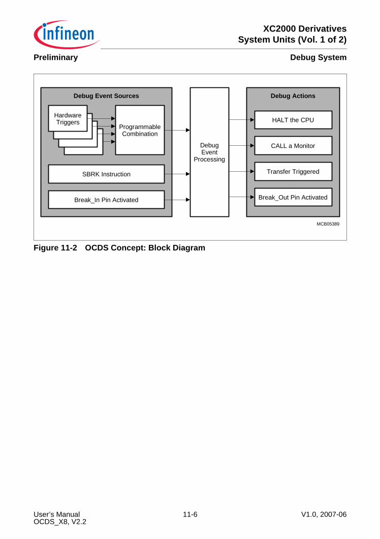
XC2000 DerivativesSystem Units (Vol. 1 of 2)
Debug SystemPreliminary
Figure 11-2 OCDS Concept: Block Diagram
Debug Event Sources Debug Actions
MCB05389
DebugEvent
Processing
SBRK Instruction
Break_In Pin Activated
HALT the CPU
CALL a Monitor
Transfer Triggered
Break_Out Pin Activated
ProgrammableCombination
HardwareTriggers
User’s Manual 11-6 V1.0, 2007-06OCDS_X8, V2.2
XC2000 DerivativesSystem Units (Vol. 1 of 2)
Debug SystemPreliminary
11.2.1 Debug EventsThe Debug Events can come from a few different sources.
Hardware BreakpointsThe Hardware Breakpoint is a debug-event, raised when a single or a combination ofmultiple trigger-signals are matching with the programmed conditions.The following hardware trigger sources can be used:
SBRK InstructionThis is a mechanism through which the software can explicitly generate a debug event.It can be used for instance by a debugger to temporarily patch code held in RAM in orderto implement Software Breakpoints.A special SBRK (Software BReaK) instruction is defined with opcode 0x8C00. When thisinstruction has been decoded and it reaches the Execute stage, the whole pipeline iscanceled including the SBRK itself. Hence in fact the SBRK instruction is never“executed” by itself.The further behavior is dependent on how OCDS has been programmed:• if the OCDS is enabled and the software breakpoints are also enabled, then the CPU
goes into Halt Mode• if the OCDS is disabled or the software breakpoints are disabled, then the Software
Break Trap (SBRKTRAP) is executed-Class A Trap, number 08H
Break Pin InputAn external debug break pin (BRKIN) is provided to allow the debugger toasynchronously interrupt the processor.
Table 11-1 Hardware TriggersTrigger Source SizeTask Identifier 16 bitsInstruction Pointer 24 bitsData address of reads (two busses monitored) 2 × 24 bitsData address of writes 24 bitsData value (reads or writes) 16 bits
User’s Manual 11-7 V1.0, 2007-06OCDS_X8, V2.2
XC2000 DerivativesSystem Units (Vol. 1 of 2)
Debug SystemPreliminary
11.2.2 Debug ActionsWhen the OCDS is enabled and a debug event is generated, one of the following actionsis taken:
Trigger TransferOne of the actions that can be specified to occur on a debug event being raised is totrigger the Cerberus:• to execute a Data Transfer - this can be used in critical routines where the system
cannot be interrupted to transfer a memory location• to inject an instruction to the Core - using this mechanism, an arbitrary instruction can
be injected into the XC2000 pipeline
Halt ModeUpon this Action the OCDS Module sends a Break-Request to the Core.The Core accepts this request, if the OCDS Break Level is higher than current CPUpriority level. In case a Break-Request is accepted, the system suspends execution withhalting the instruction flow.The Halt Mode can be still interrupted by higher priority user interrupts. It then relies onthe external debugger system to interrogate the target purely through reading andupdating via the debug interface.
Call a MonitorOne of the possible actions to be taken when a debug event is raised is to call a MonitorProgram.This short entry to a Monitor allows a flexible debug environment to be defined which iscapable of satisfying many of the requirements for efficient debugging of a real timesystem. In the common case the Monitor has the highest priority and can not beinterrupted from any other requesting source.It is also possible to have an Interruptible Monitor Program. In such a case safety criticalcode can be still served while the Monitor (Debugger) is active, which gives a maximumflexibility to the user.
Activate External PinThis action activates the external pin BRKOUT of the OCDS Break-Interface. It can beused in critical routines where the system cannot be interrupted to signal to the externalworld that a particular event has happened. The feature could also be useful tosynchronize the internal and external debug hardware.
User’s Manual 11-8 V1.0, 2007-06OCDS_X8, V2.2
XC2000 DerivativesSystem Units (Vol. 1 of 2)
Debug SystemPreliminary
11.3 CerberusCerberus is the module which provides and controls all the operations necessary tointeract between the external debugger (via the Debug Interface), the OCDS Moduleand the internal system of XC2000.
Features• JTAG interface is used as control and data channel• Generic memory read/write functionality (RW mode) with access to the whole address
space• Reading and writing of general-purpose registers (GPRs)• Injection of arbitrary instructions• External host controls all transactions• All transactions are available at normal run time and in halt mode• Priority of transactions can be configured• Full support for communication between the monitor and an external host (debugger)• Optional error protection• Tracing memory locations through transferring values to the external bus• Analysis Register for internal bus locking situationsThe target application of Cerberus is to use the JTAG interface as an independent portfor On Chip Debug Support. The external debugger can access the OCDS registers andarbitrary memory locations with the injection mechanism.
11.3.1 Functional OverviewCerberus is operated by an external debugger across the JTAG Interface. TheDebugger supplies Cerberus IO Instructions and performs bidirectional data-transfers.The Cerberus distinguishes between two main modes of operation:
Read/Write Mode of OperationRead/Write (RW) Mode is the most typical way to operate Cerberus. This mode is usedto read and write memory locations or to inject instructions. The injection interface to thecore is actively used in this mode.In this mode an external Debugger (host), using JTAG Interface, can:• read and write memory locations from the target system (data-transfer);• inject arbitrary instructions to be executed by the Core.All Cerberus IO Instructions can be used in RW mode. The dedicated IO_READ_IPinstruction is provided in RW mode to read the IP of the CPU while in Break.
User’s Manual 11-9 V1.0, 2007-06OCDS_X8, V2.2
XC2000 DerivativesSystem Units (Vol. 1 of 2)
Debug SystemPreliminary
The access to any memory location is performed with injected instructions, as PECtransfer. The following Cerberus IO Instructions can be used in their generic meaning:• IO_READ_WORD, IO_WRITE_WORD• IO_READ_BLOCK, IO_WRITE_BLOCK• IO_WRITE_BYTEWithin these instructions, the host writes/reads data to/from a dedicatedregister/memory, while the Cerberus itself takes care of the rest: to perform a PECtransfer by injection of the appropriate instructions to the Core.
Communication Mode of OperationIn this mode the external host (debugger) communicates with a program (Monitor)running on the CPU. The data-transfers are made via a PDBus+ register. The externalhost is master of all transactions, requesting the monitor to write or read a value.The difference to Read/Write Mode of Operation is that the read or write request nowis not actively executed by the Cerberus, but it sets request bits in a CPU accessibleregister to signal the Monitor, that the host wants to send (IO_WRITE_WORD) or receive(IO_READ_WORD) a value. The Monitor has to poll this status register and performrespectively the proper actionsCommunication Mode is the default mode after reset. Only the IO_WRITE_WORD andIO_READ_WORD Instructions are effectively used in Communication Mode.The Host and the Monitor exchange data directly with the dedicated data-register. For asynchronization of Host (Debugger) and Monitor accesses, there are associated controlbits in a Cerberus status register.
User’s Manual 11-10 V1.0, 2007-06OCDS_X8, V2.2
XC2000 DerivativesSystem Units (Vol. 1 of 2)
Instruction Set SummaryPreliminary
12 Instruction Set SummaryThis chapter briefly summarizes the XC2000’s instructions ordered by instructionclasses. This provides a basic understanding of the XC2000’s instruction set, the powerand versatility of the instructions and their general usage.A detailed description of each single instruction, including its operand data type,condition flag settings, addressing modes, length (number of bytes) and object codeformat is provided in the “Instruction Set Manual” for the XC2000 Family. This manualalso provides tables ordering the instructions according to various criteria, to allow quickreferences.
Summary of Instruction ClassesGrouping the various instruction into classes aids in identifying similar instructions (e.g.SHR, ROR) and variations of certain instructions (e.g. ADD, ADDB). This provides aneasy access to the possibilities and the power of the instructions of the XC2000.Note: The used mnemonics refer to the detailed description.
Table 12-1 Arithmetic InstructionsAddition of two words or bytes: ADD ADDBAddition with Carry of two words or bytes: ADDC ADDCBSubtraction of two words or bytes: SUB SUBBSubtraction with Carry of two words or bytes: SUBC SUBCB16 × 16 bit signed or unsigned multiplication: MUL MULU16/16 bit signed or unsigned division: DIV DIVU32/16 bit signed or unsigned division: DIVL DIVLU1’s complement of a word or byte: CPL CPLB2’s complement (negation) of a word or byte: NEG NEGB
Table 12-2 Logical InstructionsBitwise ANDing of two words or bytes: AND ANDBBitwise ORing of two words or bytes: OR ORBBitwise XORing of two words or bytes: XOR XORB
User’s Manual 12-1 V1.0, 2007-06InstrSummary_X, V2.0
XC2000 DerivativesSystem Units (Vol. 1 of 2)
Instruction Set SummaryPreliminary
Table 12-3 Compare and Loop Control InstructionsComparison of two words or bytes: CMP CMPBComparison of two words with post-increment by either 1 or 2:
CMPI1 CMPI2
Comparison of two words with post-decrement by either 1 or 2:
CMPD1 CMPD2
Table 12-4 Boolean Bit Manipulation InstructionsManipulation of a maskable bit field in either the high or the low byte of a word:
BFLDH BFLDL
Setting a single bit (to ‘1’): BSET –Clearing a single bit (to ‘0’): BCLR –Movement of a single bit: BMOV –Movement of a negated bit: BMOVN –ANDing of two bits: BAND –ORing of two bits: BOR –XORing of two bits: BXOR –Comparison of two bits: BCMP –
Table 12-5 Shift and Rotate InstructionsShifting right of a word: SHR –Shifting left of a word: SHL –Rotating right of a word: ROR –Rotating left of a word: ROL –Arithmetic shifting right of a word (sign bit shifting): ASHR –
Table 12-6 Prioritize InstructionDetermination of the number of shift cycles required to normalize a word operand (floating point support):
PRIOR –
User’s Manual 12-2 V1.0, 2007-06InstrSummary_X, V2.0
XC2000 DerivativesSystem Units (Vol. 1 of 2)
Instruction Set SummaryPreliminary
Note: The data movement instructions can be used with a big number of differentaddressing modes including indirect addressing and automatic pointer in-/decrementing.
Table 12-7 Data Movement InstructionsStandard data movement of a word or byte: MOV MOVBData movement of a byte to a word location with either sign or zero byte extension:
MOVBS MOVBZ
Table 12-8 System Stack InstructionsPushing of a word onto the system stack: PUSH –Popping of a word from the system stack: POP –Saving of a word on the system stack, and then updating the old word with a new value (provided for register bank switching):
SCXT –
Table 12-9 Jump InstructionsConditional jumping to an either absolutely, indirectly, or relatively addressed target instruction within the current code segment:
JMPA JMPI JMPR
Unconditional jumping to an absolutely addressed target instruction within any code segment:
JMPS – –
Conditional jumping to a relatively addressed target instruction within the current code segment depending on the state of a selectable bit:
JB JNB –
Conditional jumping to a relatively addressed target instruction within the current code segment depending on the state of a selectable bit with a post-inversion of the tested bit in case of jump taken (semaphore support):
JBC JNBS –
User’s Manual 12-3 V1.0, 2007-06InstrSummary_X, V2.0
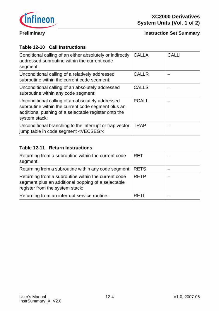
XC2000 DerivativesSystem Units (Vol. 1 of 2)
Instruction Set SummaryPreliminary
Table 12-10 Call InstructionsConditional calling of an either absolutely or indirectly addressed subroutine within the current code segment:
CALLA CALLI
Unconditional calling of a relatively addressed subroutine within the current code segment:
CALLR –
Unconditional calling of an absolutely addressed subroutine within any code segment:
CALLS –
Unconditional calling of an absolutely addressed subroutine within the current code segment plus an additional pushing of a selectable register onto the system stack:
PCALL –
Unconditional branching to the interrupt or trap vector jump table in code segment <VECSEG>:
TRAP –
Table 12-11 Return InstructionsReturning from a subroutine within the current code segment:
RET –
Returning from a subroutine within any code segment: RETS –Returning from a subroutine within the current code segment plus an additional popping of a selectable register from the system stack:
RETP –
Returning from an interrupt service routine: RETI –
User’s Manual 12-4 V1.0, 2007-06InstrSummary_X, V2.0
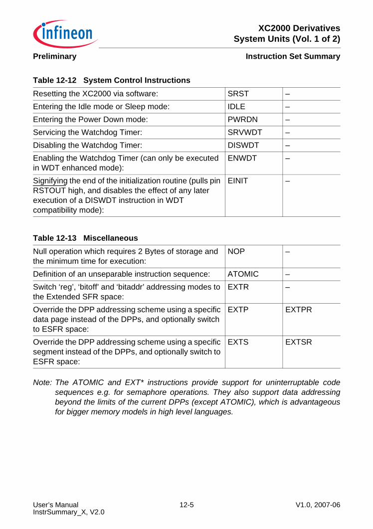
XC2000 DerivativesSystem Units (Vol. 1 of 2)
Instruction Set SummaryPreliminary
Note: The ATOMIC and EXT* instructions provide support for uninterruptable codesequences e.g. for semaphore operations. They also support data addressingbeyond the limits of the current DPPs (except ATOMIC), which is advantageousfor bigger memory models in high level languages.
Table 12-12 System Control InstructionsResetting the XC2000 via software: SRST –Entering the Idle mode or Sleep mode: IDLE –Entering the Power Down mode: PWRDN –Servicing the Watchdog Timer: SRVWDT –Disabling the Watchdog Timer: DISWDT –Enabling the Watchdog Timer (can only be executed in WDT enhanced mode):
ENWDT –
Signifying the end of the initialization routine (pulls pin RSTOUT high, and disables the effect of any later execution of a DISWDT instruction in WDT compatibility mode):
EINIT –
Table 12-13 MiscellaneousNull operation which requires 2 Bytes of storage and the minimum time for execution:
NOP –
Definition of an unseparable instruction sequence: ATOMIC –Switch ‘reg’, ‘bitoff’ and ‘bitaddr’ addressing modes to the Extended SFR space:
EXTR –
Override the DPP addressing scheme using a specific data page instead of the DPPs, and optionally switch to ESFR space:
EXTP EXTPR
Override the DPP addressing scheme using a specific segment instead of the DPPs, and optionally switch to ESFR space:
EXTS EXTSR
User’s Manual 12-5 V1.0, 2007-06InstrSummary_X, V2.0
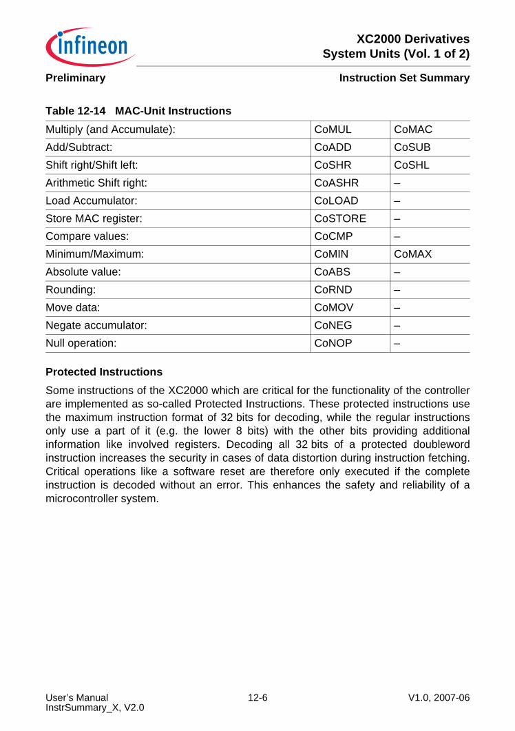
XC2000 DerivativesSystem Units (Vol. 1 of 2)
Instruction Set SummaryPreliminary
Protected InstructionsSome instructions of the XC2000 which are critical for the functionality of the controllerare implemented as so-called Protected Instructions. These protected instructions usethe maximum instruction format of 32 bits for decoding, while the regular instructionsonly use a part of it (e.g. the lower 8 bits) with the other bits providing additionalinformation like involved registers. Decoding all 32 bits of a protected doublewordinstruction increases the security in cases of data distortion during instruction fetching.Critical operations like a software reset are therefore only executed if the completeinstruction is decoded without an error. This enhances the safety and reliability of amicrocontroller system.
Table 12-14 MAC-Unit InstructionsMultiply (and Accumulate): CoMUL CoMACAdd/Subtract: CoADD CoSUBShift right/Shift left: CoSHR CoSHLArithmetic Shift right: CoASHR –Load Accumulator: CoLOAD –Store MAC register: CoSTORE –Compare values: CoCMP –Minimum/Maximum: CoMIN CoMAXAbsolute value: CoABS –Rounding: CoRND –Move data: CoMOV –Negate accumulator: CoNEG –Null operation: CoNOP –
User’s Manual 12-6 V1.0, 2007-06InstrSummary_X, V2.0
XC2000 DerivativesSystem Units (Vol. 1 of 2)
Device SpecificationPreliminary
13 Device SpecificationThe device specification describes the electrical parameters of the device. It lists DCcharacteristics like input, output or supply voltages or currents, and AC characteristicslike timing characteristics and requirements.Other than the architecture, the instruction set, or the basic functions of the XC2000 coreand its peripherals, these DC and AC characteristics are subject to changes due todevice improvements or specific derivatives of the standard device.Therefore, these characteristics are not contained in this manual, but rather provided ina separate Data Sheet, which can be updated more frequently.Please refer to the current version of the Data Sheet of the respective device for allelectrical parameters.Note: In any case the specific characteristics of a device should be verified, before a new
design is started. This ensures that the used information is up to date.
The XC2000 derivatives are shipped in several packages. Figure 13-1 and Figure 13-2show the basic pin diagrams of the XC2000. They show the location of the differentsupply and IO pins. A detailed description of all the pins and their selectable functionscan be found in the corresponding Data Sheet.Note: Not all alternate functions shown in Figure 13-1 are supported by all derivatives.
Please refer to the corresponding descriptions in the data sheets.
User’s Manual 13-1 V1.0, 2007-06DeviceSpecX2K, V1.0
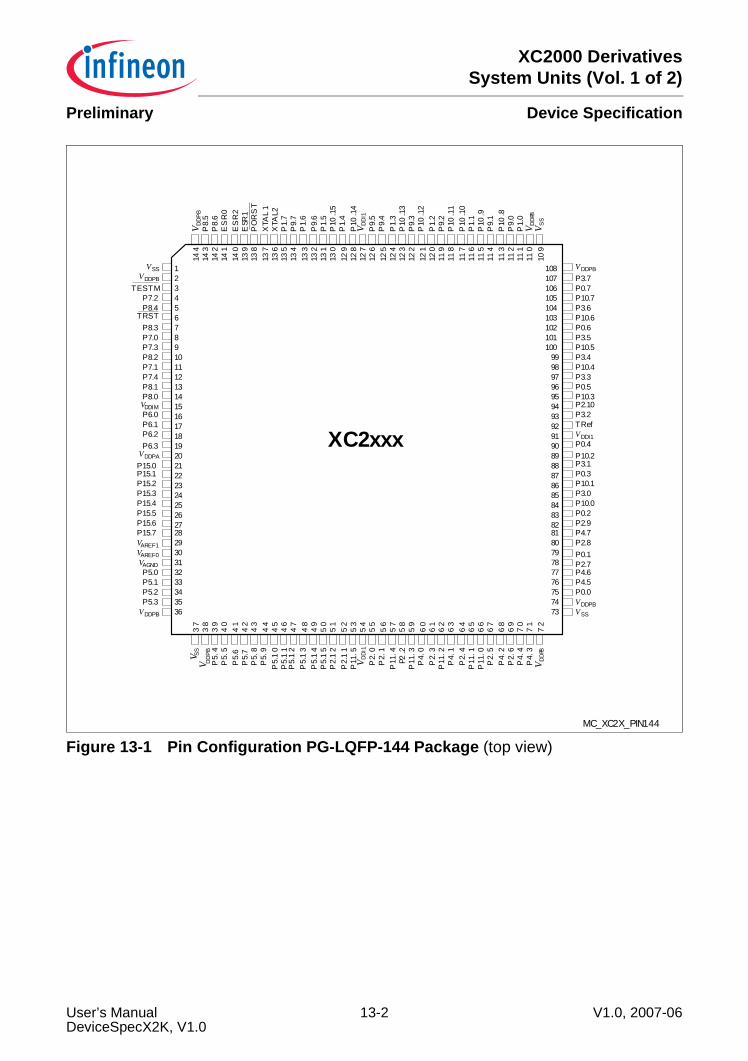
XC2000 DerivativesSystem Units (Vol. 1 of 2)
Device SpecificationPreliminary
Figure 13-1 Pin Configuration PG-LQFP-144 Package (top view)MC_XC2X_PIN144
VSS
VDDPB
P0.0P4.5P4.6P2.7
P5.2P5.1P5.0
VAGND
VAREF0
VAREF1
P15.5P15.4P15.3P15.2P15.1P15.0
P6.2P6.1P6.0VDDIM
P8.0P8.1P7.4P7.1P8.2P7.3P7.0P8.3
P7.2TESTM
VDDPB
VSS
VDDPA
P6.3
P15.7P15.6
VDDPB
P5.3
P2.8P0.1
P4.7P2.9P0.2P10.0P3.0P10.1P0.3P3.1P10.2P0.4VDDI1
TRefP3.2P2.10P10.3P0.5P3.3P10.4P3.4P10.5P3.5P0.6P10.6P3.6P10.7P0.7P3.7VDDPB
V DD
PBP
8.5
P8.
6E
SR
0E
SR
2E
SR1
PO
RS
TX
TAL
1X
TAL2
P1.
7P
9.7
P1.
6P
9.6
P1.
5P
10.1
5P
1.4
P10
.14
V DD
I1P
9.5
P9.
4P
1.3
P10
.13
P9.
3P
10.1
2P
1.2
P9.
2P
10.1
1P
10.1
0P
1.1
P10
.9P
9.1
P10
.8P
9.0
P1.
0V D
DPB
V SS
P2.
1
V SS
V DD
PBP
5.4
P5.
5P
5.6
P5.
7P
5.8
P5.
9P
5.1
0P
5.1
1P
5.1
2P
5.1
3P
5.1
4P
5.1
5P
2.1
2P
2.1
1P
11.5
V DDI
1P
2.0
P11
.4P2
.2P
11.3
P4.
0P
2.3
P11
.2P
4.1
P2.
4P
11.1
P11
.0P
2.5
P4.
2P
2.6
P4.
4P
4.3
V DD
PB
XC2xxx
108107106105104103102101100
99989796959493929190898887868584838281807978777675747336
3534333231302928272625242322212019181716151413121110987654321
144
143
142
141
140
139
138
137
136
135
134
133
132
131
130
129
128
127
126
125
124
123
122
121
120
119
118
117
116
115
114
113
112
111
110
109
37
38
39
40
41
42
43
44
45
46
47
48
49
50
51
52
53
54
55
56
57
58
59
60
61
62
63
64
65
66
67
68
69
70
71
72
P8.4TRST
User’s Manual 13-2 V1.0, 2007-06DeviceSpecX2K, V1.0
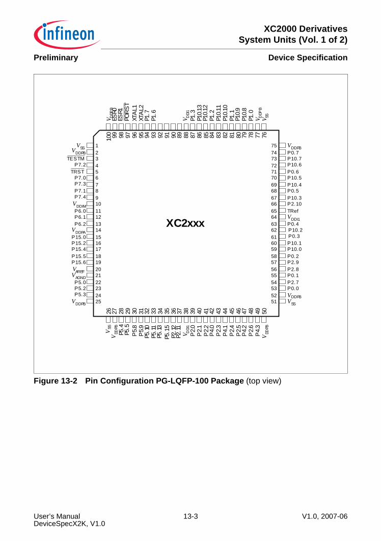
XC2000 DerivativesSystem Units (Vol. 1 of 2)
Device SpecificationPreliminary
Figure 13-2 Pin Configuration PG-LQFP-100 Package (top view)
VDDPB 25P5.3 24P5.2 23P5.0 22
VAGND 212019
P15.5 18
VDDPA
1716
P15.0 15
P15.4
14P6.2 13P6.1 12P6.0 11
VDDIM 1098
P7.3 765
P7.2 4TESTM 3
VDDPB 2VSS 1
P7.0TRST
VAREF
P15.6
100 99 98 97 96 95 94 93 92 91 90 89 88 87 86 85 84 83 82 81 80 79 78 77 76
V DDP
BES
R0ES
R1PO
RST
XTA
L1XT
AL2
P1.7
P1.6
V DDI
1P1
.3P1
0.13
P10.
12P1
.2P1
0.11
P10.
10P1
.1P1
0.9
P10.
8P1
.0V D
DPB
V SS
26 27 28 29 30 31 32 33 34 35 36 37 38 39 40 41 42 43 44 45P
2.446 47 48 49 50
VSS
VDD
PB
P5.8
P5.9
P5.10
P5.11
P5.13
P5.1
5P2
.12P2
.11V D
DI1
P2.0
P2.1
P2.2
P4.0
P2.3
P4.1
P2.5
P4.2
P2.6
P4.3
VDD
PB
75747372717069686766656463626160595857565554535251 VSS
VDDPB
P0.0P2.7P0.1P2.8P2.9P0.2P10.0P10.1
P10.2P0.4VDDI1
TRefP2.10P10.3P0.5P10.4P10.5P0.6P10.6P10.7P0.7VDDPB
XC2xxx
P7.4P7.1
P15.2P0.3
P5.4
P5.5
User’s Manual 13-3 V1.0, 2007-06DeviceSpecX2K, V1.0

XC2000 DerivativesSystem Units (Vol. 1 of 2)
Device SpecificationPreliminary
User’s Manual 13-4 V1.0, 2007-06DeviceSpecX2K, V1.0
XC2000 DerivativesSystem Units (Vol. 1 of 2)
Keyword IndexPreliminary
Keyword IndexThis section lists a number of keywords which refer to specific details of the XC2000 interms of its architecture, its functional units or functions. This helps to quickly find theanswer to specific questions about the XC2000.This User’s Manual consists of two Volumes, “System Units” and “Peripheral Units”. Foryour convenience this keyword index refers to both volumes, so you can immediatelyfind the reference to the desired section in the corresponding document ([1] or [2]).Note: Registers are listed in a separate index: Register Index.
AAcronyms 1-9 [1]Addressing Modes
CoREG Addressing Mode 4-50 [1]DSP Addressing Modes 4-46 [1]Indirect Addressing Modes 4-44 [1]Long Addressing Modes 4-41 [1]Short Addressing Modes 4-39 [1]
ALU 4-57 [1]
BBaudrate
Bootstrap Loader 10-9 [1]Bit
Handling 4-60 [1]Manipulation Instructions 12-2 [1]protected 4-61 [1]reserved 2-17 [1]
Block Diagram ITC / PEC 5-3 [1]Bootstrap Loader 10-4 [1]
CCAN
Block diagram 20-2 [2]Clock control 20-102 [2]Features 20-2 [2]Functional description 20-4 [2]Interrupt structure 20-105 [2]Module implementation 20-106 [2]MultiCAN
Analysis mode 20-19 [2]
Bit timing 20-10 [2]Block diagram 20-7 [2]Error handling 20-12 [2]Gateway mode 20-42 [2]Interrupts 20-13 [2]Message acceptance filtering 20-22 [2]Message object FIFO 20-37 [2]Message object lists 20-14 [2]Node control 20-10 [2]
Overview 20-4 [2]Registers
LISTiH 20-58 [2]LISTiL 20-59 [2]MCR 20-56 [2]MITR 20-57 [2]MOAMRnH 20-95 [2]MOAMRnL 20-95 [2]MOARnH 20-97 [2]MOARnL 20-98 [2]MOCTRnH 20-80 [2], 20-82 [2]MOCTRnL 20-81 [2], 20-82 [2]MODATAnHH 20-101 [2]MODATAnHL 20-101 [2]MODATAnLH 20-100 [2]MODATAnLL 20-100 [2]MOFCRnH 20-89 [2]MOFCRnL 20-91 [2]MOFGPRnH 20-93 [2]MOFGPRnL 20-93 [2]MOIPRnH 20-87 [2]
User’s Manual L-1 V1.0, 2007-06
XC2000 DerivativesSystem Units (Vol. 1 of 2)
Keyword IndexPreliminary
MOIPRnL 20-87 [2]MSIDk 20-61 [2]MSIMASKH 20-62 [2]MSIMASKL 20-62 [2]MSPNDkH 20-60 [2]MSPNDkL 20-60 [2]NBTRxH 20-72 [2]NBTRxL 20-73 [2]NCRx 20-63 [2]NECNTxH 20-74 [2]NECNTxL 20-74 [2]NFCRxH 20-76 [2]NFCRxL 20-77 [2]NIPRx 20-70 [2]NPCRx 20-71 [2]NSRx 20-66 [2]PANCTRH 20-51 [2]PANCTRL 20-51 [2]
CAPCOM12Capture Mode 17-14 [2]Counter Mode 17-9 [2]
CAPCOM2 2-17 [1]Capture Mode
GPT1 14-26 [2]GPT2 (CAPREL) 14-48 [2]
Capture/Compare Registers 17-11 [2]CCU6 2-19 [1]Clock
generation 2-32 [1]Clock System 6-2 [1]
Clock Control Unit 6-13 [1]Clock Generation Unit 6-2 [1]Clock Output 6-15 [1]Crystal oscillator 6-3 [1]Crystal Oscillator run detection 6-11 [1]Emergency Clock Operation 6-14 [1]PLL 6-5 [1]
Switching parameters 6-12 [1]Concatenation of Timers 14-22 [2],
14-47 [2]Context
Pointer Updating 4-34 [1]Switch 4-33 [1]
Switching 5-33 [1]Count direction 14-6 [2], 14-36 [2]Counter 14-20 [2], 14-45 [2]Counter Mode (GPT1) 14-10 [2], 14-40 [2]CPU 2-2 [1], 4-1 [1]
DData Management Unit (Introduction)
2-9 [1]Data Page 4-42 [1]Development Support 1-8 [1]Direction
count 14-6 [2], 14-36 [2]Disable
Interrupt 5-30 [1]Division 4-62 [1]Double-Register Compare 17-24 [2]DPP 4-42 [1]
EEBC
Bus Signals 9-3 [1]Memory Table 9-33 [1]
EnableInterrupt 5-30 [1]
End of PEC Interrupt Sub Node 5-29 [1]ESRx 5-1 [1]External
Bus 2-14 [1]Interrupts 5-36 [1]
External Request Unit (ERU) 6-64 [1]ERS 6-72 [1]ETL 6-74 [1]Internal Connections 6-76 [1]OGU 6-77 [1]Operation 6-64 [1]Pin Connetions 6-66 [1]
External Service Request (ESR) 6-52 [1]ESR Pad Control 6-57 [1]ESR Reset 6-55 [1]ESR Trap 6-56 [1]ESR Wake-up 6-56 [1]Operation 6-52 [1]
User’s Manual L-2 V1.0, 2007-06
XC2000 DerivativesSystem Units (Vol. 1 of 2)
Keyword IndexPreliminary
FFlags 4-56 [1]–4-59 [1]Fractional divider
Block diagram 20-108 [2]Operating modes 20-110 [2]Suspend mode 20-111 [2]
GGated timer mode (GPT1) 14-9 [2]Gated timer mode (GPT2) 14-39 [2]Global State Controller (GSC) 6-156 [1]
Commands 6-157 [1]Operation 6-156 [1]Priorities 6-156 [1]
GPT 2-20 [1]GPT1 14-2 [2]GPT2 14-32 [2]
HHardware
Traps 5-41 [1]
IIncremental Interface Mode (GPT1)
14-11 [2]Instruction 12-1 [1]
Bit Manipulation 12-2 [1]Pipeline 4-11 [1]protected 12-6 [1]
InterfaceExternal Bus 9-1 [1]
InterruptArbitration 5-4 [1]Enable/Disable 5-30 [1]External 5-36 [1]Jump Table Cache 5-17 [1]Latency 5-39 [1]Node Sharing 5-35 [1]Priority 5-7 [1]Processing 5-1 [1]RTC 15-13 [2]System 2-8 [1], 5-2 [1]
LLatency
Interrupt, PEC 5-39 [1]LXBus 2-14 [1]
MMemory 2-10 [1]Multiplication 4-62 [1]
OOCDS
Requests 5-38 [1]
PPEC 2-10 [1], 5-19 [1]
Latency 5-39 [1]Transfer Count 5-20 [1]
PeripheralEvent Controller --> PEC 5-19 [1]Summary 2-15 [1]
Pins 8-1 [1]Pipeline 4-11 [1]Port 2-30 [1]Ports
Configuring a Pin 7-15 [1]I/O Description Entry 7-6 [1]Output register Pn_OUT 7-10 [1]Pad driver control 7-7 [1]Structure
Analog 7-4 [1]Hardware Override 7-3 [1]Standard 7-2 [1]
Power Control 6-90 [1]Changing Core Voltage 6-126 [1]Control of Core Voltage 6-115 [1]EVR 6-115 [1]Monitoring Core Voltage 6-97 [1]PSC 6-128 [1]PVC 6-97 [1]Supply Watchdog (SWD) 6-91 [1]
Program Management Unit (Introduction) 2-9 [1]
User’s Manual L-3 V1.0, 2007-06
XC2000 DerivativesSystem Units (Vol. 1 of 2)
Keyword IndexPreliminary
ProtectedBits 4-61 [1]instruction 12-6 [1]
RReal Time Clock (->RTC) 2-22 [1], 15-1 [2]Reserved bits 2-17 [1]Reset 6-33 [1]
Modules behavior 6-40 [1]Reset Operation 6-33 [1]Reset Types 6-33 [1]
CPU Reset 6-38 [1]ESR Reset 6-37 [1]Memory Parity Reset 6-38 [1]OCDS Controlled Reset 6-38 [1]Power-on Reset 6-37 [1]Software Reset 6-38 [1]Supply Watchdog Reset 6-37 [1]Voltage Monitoring Reset 6-37 [1]Watchdog Timer Reset 6-38 [1]
RTC 2-22 [1], 15-1 [2]Registers
T14 15-8 [2]T14REL 15-8 [2]
SSCU
Identification 6-218 [1]Interrupt 6-186 [1]
Buffering 6-210 [1]Operation 6-187 [1]
Register Access 6-181 [1]Register Overview 6-220 [1]Trap 6-186 [1]
Buffering 6-210 [1]Operation 6-200 [1]
Segmentation 4-37 [1]Sharing
Interrupt Nodes 5-35 [1]Software
Traps 5-41 [1]SR0 5-46 [1]SR1 5-46 [1]
Stack 4-52 [1]
TTemperature Compensation Unit 6-165 [1]Timer 14-2 [2], 14-32 [2]
Auxiliary Timer 14-15 [2], 14-41 [2]Concatenation 14-22 [2], 14-47 [2]Core Timer 14-4 [2], 14-34 [2]Counter Mode (GPT1) 14-10 [2], 14-40 [2]Gated Mode (GPT1) 14-9 [2]Gated Mode (GPT2) 14-39 [2]Incremental Interface Mode (GPT1) 14-11 [2]Mode (GPT1) 14-8 [2]Mode (GPT2) 14-38 [2]
Tools 1-8 [1]Traps 5-41 [1]
WWake-up Timer 6-176 [1]Watchdog 2-29 [1]Watchdog Timer 6-168 [1]
Operation 6-168 [1]Disable Mode 6-171 [1]Normal Mode 6-170 [1]Prewarning Mode 6-171 [1]Suspend Mode 6-172 [1]
User’s Manual L-4 V1.0, 2007-06
XC2000 DerivativesSystem Units (Vol. 1 of 2)
Register IndexPreliminary
Register IndexThis section lists the registers of the XC2000. This helps to quickly find the reference tothe description of the respective register.This User’s Manual consists of two Volumes, “System Units” and “Peripheral Units”. Foryour convenience this register index refers to both volumes, so you can immediately findthe reference to the desired section in the corresponding document ([1] or [2]).Note: Keywords are listed in a separate index: Keyword Index.
AADC0_KSCFG 16-24 [2]ADCx_ALR0 16-77 [2]ADCx_ASENR 16-37 [2]ADCx_CHCTRx 16-68 [2]ADCx_CHINCR 16-73 [2]ADCx_CHINFR 16-72 [2]ADCx_CHINPRx 16-74 [2]ADCx_CRCRx 16-43 [2]ADCx_CRMRx 16-45 [2]ADCx_CRPRx 16-44 [2]ADCx_EMCTR 16-102 [2]ADCx_EMENR 16-103 [2]ADCx_EVINCR 16-93 [2]ADCx_EVINFR 16-92 [2]ADCx_EVINPRx 16-94 [2]ADCx_GLOBCTR 16-26 [2]ADCx_GLOBSTR 16-28 [2]ADCx_INPRx 16-70 [2]ADCx_LCBRx 16-71 [2]ADCx_PISEL 16-31 [2]ADCx_Q0Rx 16-57 [2]ADCx_QBURx 16-59 [2]ADCx_QINRx 16-61 [2]ADCx_QMRx 16-52 [2]ADCx_QSRx 16-55 [2]ADCx_RCRx 16-90 [2]ADCx_RESRAVx 16-87 [2]ADCx_RESRAx 16-87 [2]ADCx_RESRVx 16-86 [2]ADCx_RESRx 16-86 [2]ADCx_RSPRx 16-38 [2]
ADCx_RSSR 16-88 [2]ADCx_SYNCTR 16-104 [2]ADCx_VFR 16-89 [2]ADDRSELx 9-22 [1]
BBANKSELx 5-34 [1]
CCAN_LISTiH 20-58 [2]CAN_LISTiL 20-59 [2]CAN_MCR 20-56 [2]CAN_MITR 20-57 [2]CAN_MOAMRnH 20-95 [2]CAN_MOAMRnL 20-95 [2]CAN_MOARnH 20-97 [2]CAN_MOARnL 20-98 [2]CAN_MOCTRnH 20-80 [2]CAN_MOCTRnL 20-81 [2]CAN_MODATAnHH 20-101 [2]CAN_MODATAnHL 20-101 [2]CAN_MODATAnLH 20-100 [2]CAN_MODATAnLL 20-100 [2]CAN_MOFCRnH 20-89 [2]CAN_MOFCRnL 20-91 [2]CAN_MOFGPRnH 20-93 [2]CAN_MOFGPRnL 20-93 [2]CAN_MOIPRnH 20-87 [2]CAN_MOIPRnL 20-87 [2]CAN_MOSTATnH 20-82 [2]CAN_MOSTATnL 20-82 [2]CAN_MSIDk 20-61 [2]
User’s Manual L-5 V1.0, 2007-06
XC2000 DerivativesSystem Units (Vol. 1 of 2)
Register IndexPreliminary
CAN_MSIMASKH 20-62 [2]CAN_MSIMASKL 20-62 [2]CAN_MSPNDkH 20-60 [2]CAN_MSPNDkL 20-60 [2]CAN_NBTRxH 20-72 [2]CAN_NBTRxL 20-73 [2]CAN_NCRx 20-63 [2]CAN_NECNTxH 20-74 [2]CAN_NECNTxL 20-74 [2]CAN_NFCRxH 20-76 [2]CAN_NFCRxL 20-77 [2]CAN_NIPRx 20-70 [2]CAN_NPCRx 20-71 [2]CAN_NSRx 20-66 [2]CAN_PANCTRH 20-51 [2]CAN_PANCTRL 20-51 [2]CAPREL 14-56 [2]CC2_CCyIC 17-36 [2]CC2_DRM 17-25 [2]CC2_IOC 17-31 [2]CC2_KSCCFG 17-39 [2]CC2_M4/5/6/7 17-11 [2]CC2_OUT 17-27 [2]CC2_SEE 17-29 [2]CC2_SEM 17-29 [2]CC2_T78CON 17-5 [2]CC2_T7IC 17-10 [2]CC2_T8IC 17-10 [2]CCU6x_CC63R 18-65 [2]CCU6x_CC63SR 18-65 [2]CCU6x_CC6xR 18-34 [2]CCU6x_CC6xSR 18-35 [2]CCU6x_CMPMODIF 18-40 [2]CCU6x_CMPSTAT 18-38 [2]CCU6x_IEN 18-98 [2]CCU6x_INP 18-101 [2]CCU6x_IS 18-91 [2]CCU6x_ISR 18-96 [2]CCU6x_ISS 18-94 [2]CCU6x_KSCFG 18-111 [2]CCU6x_KSCSR 18-113 [2]CCU6x_MCFG 18-114 [2]CCU6x_MCMCTR 18-84 [2]
CCU6x_MCMOUT 18-87 [2]CCU6x_MCMOUTS 18-86 [2]CCU6x_MODCTR 18-78 [2]CCU6x_PISELH 18-109 [2]CCU6x_PISELL 18-107 [2]CCU6x_PSLR 18-83 [2]CCU6x_T12 18-33 [2]CCU6x_T12DTC 18-36 [2]CCU6x_T12MSEL 18-41 [2]CCU6x_T12PR 18-33 [2]CCU6x_T13 18-63 [2]CCU6x_T13PR 18-64 [2]CCU6x_TCTR0 18-42 [2]CCU6x_TCTR2 18-45 [2]CCU6x_TCTR4 18-48 [2]CCU6x_TRPCTR 18-80 [2]CP 4-36 [1]CPUCON1 4-26 [1]CPUCON2 4-27 [1]CRIC 14-57 [2]CSP 4-38 [1]
DDPP0/1/2/3 4-42 [1]DSTPx 5-24 [1]
EEBCMOD0 9-13 [1]EBCMOD1 9-15 [1]EOPIC 5-28 [1]
FFCONCS0 9-19 [1]FCONCS1/2/3/4/7 9-20 [1]FINT0/1ADDR 5-17 [1]FINT0/1CSP 5-17 [1]FL_KSCCFG 3-64 [1]FSR_BUSY 3-57 [1]FSR_OP 3-57 [1]FSR_PROT 3-59 [1]
GGPT12E_CAPREL 14-56 [2]
User’s Manual L-6 V1.0, 2007-06
XC2000 DerivativesSystem Units (Vol. 1 of 2)
Register IndexPreliminary
GPT12E_CRIC 14-57 [2]GPT12E_KSCCFG 14-58 [2]GPT12E_T2,-T3,-T4 14-30 [2]GPT12E_T2/3/4IC 14-31 [2]GPT12E_T2CON 14-15 [2]GPT12E_T3CON 14-4 [2]GPT12E_T4CON 14-15 [2]GPT12E_T5,-T6 14-56 [2]GPT12E_T5/6IC 14-57 [2]GPT12E_T5CON 14-41 [2]GPT12E_T6CON 14-34 [2]
IIDX0/1 4-46 [1]IMBCTRH 3-54 [1]IMBCTRL 3-52 [1]INTCTR 3-55 [1]IP 4-38 [1]
MMAH 4-69 [1]MAL 4-68 [1]MAR 3-61 [1]MCW 4-65 [1]MDC 4-63 [1]MDH 4-62 [1]MDL 4-63 [1]MEM_KSCCFG 3-63 [1]MKMEM0/1 3-76 [1]MRW 4-72 [1]MSW 4-70 [1]
OONES 4-74 [1]
PPECCx 5-20 [1]PECISNC 5-28 [1]PECON 3-78 [1]PECSEGx 5-24 [1]Pn_DIDIS
P15 7-17 [1]P5 7-17 [1]
Pn_IN 7-13 [1]Pn_IOCRx 7-14 [1]Pn_OMRH
P10 7-11 [1]P2 7-11 [1]
Pn_OMRL 7-11 [1]Pn_OUT 7-10 [1]Pn_POCON 7-8 [1]Ports
Pn_IN 7-13 [1]Pn_IOCRx 7-14 [1]Pn_OMR 7-11 [1]
PROCONx 3-62 [1]PSW 4-56 [1]
QQR0/1 4-45 [1]QX0/1 4-47 [1]
RRELH/L 15-10 [2]RTC_CON 15-5 [2]RTC_IC 15-14 [2]RTC_ISNC 15-14 [2]RTC_KSCCFG 15-15 [2]RTC_RELH/L 15-10 [2]RTC_RTCH/L 15-9 [2]RTC_T14 15-8 [2]RTC_T14REL 15-8 [2]RTCH/L 15-9 [2]
SSBRAM_DATA0 3-74 [1]SBRAM_DATA1 3-75 [1]SBRAM_RADD 3-72 [1]SBRAM_WADD 3-73 [1]SCU
RegistersDMPMIT 6-211 [1]DMPMITCLR 6-214 [1]ESRCFG0 6-61 [1]ESRCFG1 6-61 [1]ESRCFG2 6-61 [1]
User’s Manual L-7 V1.0, 2007-06
XC2000 DerivativesSystem Units (Vol. 1 of 2)
Register IndexPreliminary
ESRDAT 6-63 [1]ESREXCON1 6-58 [1]ESREXCON2 6-59 [1]EVR1CON0 6-118 [1]EVR1SET10V 6-123 [1]EVR1SET15VHP 6-125 [1]EVR1SET15VLP 6-124 [1]EVRMCON0 6-117 [1]EVRMCON1 6-119 [1]EVRMSET10V 6-120 [1]EVRMSET15VHP 6-122 [1]EVRMSET15VLP 6-121 [1]EXICON0 6-85 [1]EXICON1 6-85 [1]EXICON2 6-85 [1]EXICON3 6-85 [1]EXISEL 6-83 [1]EXOCON0 6-88 [1]EXOCON1 6-88 [1]EXOCON2 6-88 [1]EXOCON3 6-88 [1]EXTCON 6-31 [1]GSCEN 6-160 [1]GSCSTAT 6-163 [1]GSCSWREQ 6-160 [1]HPOSCCON 6-19 [1]IDCHIP 6-218 [1]IDMANUF 6-218 [1]IDMEM 6-219 [1]IDPROG 6-219 [1]INTCLR 6-192 [1]INTDIS 6-195 [1]INTNP0 6-196 [1]INTNP1 6-199 [1]INTSET 6-193 [1]INTSTAT 6-189 [1]ISSR 6-216 [1]PLLCON0 6-24 [1]PLLCON1 6-25 [1]PLLCON2 6-26 [1]PLLCON3 6-27 [1]PLLOSCCON 6-21 [1]PLLSTAT 6-22 [1]
PVC1CON0 6-100 [1]PVC1CONA1 6-106 [1]PVC1CONA2 6-106 [1]PVC1CONA3 6-106 [1]PVC1CONA4 6-106 [1]PVC1CONA5 6-106 [1]PVC1CONA6 6-106 [1]PVC1CONB1 6-112 [1]PVC1CONB3 6-112 [1]PVC1CONB4 6-112 [1]PVC1CONB5 6-112 [1]PVC1CONB6 6-112 [1]PVCMCON0 6-98 [1]PVCMCONA1 6-103 [1]PVCMCONA2 6-103 [1]PVCMCONA3 6-103 [1]PVCMCONA4 6-103 [1]PVCMCONA5 6-103 [1]PVCMCONA6 6-103 [1]PVCMCONB1 6-109 [1]PVCMCONB2 6-109 [1]PVCMCONB3 6-109 [1]PVCMCONB4 6-109 [1]PVCMCONB5 6-109 [1]PVCMCONB6 6-109 [1]RSTCNTCON 6-50 [1]RSTCON0 6-47 [1]RSTCON1 6-48 [1]RSTSTAT0 6-41 [1]RSTSTAT1 6-42 [1]RSTSTAT2 6-44 [1]RTCCLKCON 6-31 [1]SEQASTEP1 6-139 [1]SEQASTEP2 6-144 [1]SEQASTEP3 6-144 [1]SEQASTEP4 6-144 [1]SEQASTEP5 6-144 [1]SEQASTEP6 6-144 [1]SEQBSTEP1 6-147 [1]SEQBSTEP2 6-152 [1]SEQBSTEP3 6-152 [1]SEQBSTEP4 6-152 [1]SEQBSTEP5 6-152 [1]
User’s Manual L-8 V1.0, 2007-06
XC2000 DerivativesSystem Units (Vol. 1 of 2)
Register IndexPreliminary
SEQBSTEP6 6-152 [1]SEQCON 6-134 [1]SLC 6-183 [1]SLS 6-184 [1]STATCLR0 6-29 [1]STATCLR1 6-30 [1]STEP0 6-136 [1]SWDCON0 6-94 [1]SWDCON1 6-95 [1]SWRSTCON 6-51 [1]SYSCON0 6-28 [1]SYSCON1 6-185 [1]TCCR 6-166 [1]TCLR 6-167 [1]TRAPCLR 6-204 [1], 6-205 [1]TRAPDIS 6-206 [1]TRAPNP 6-207 [1]TRAPSTAT 6-202 [1]WDTCS 6-173 [1]WDTREL 6-173 [1]WDTTIM 6-175 [1]WICR 6-178 [1]WUCR 6-178 [1]WUOSCCON 6-18 [1]
SCU_STSTAT 6-46 [1]SP 4-53 [1]SPSEG 4-53 [1]SRCPx 5-24 [1]STKOV 4-55 [1]STKUN 4-55 [1]STSTAT 6-46 [1]
TT14 15-8 [2]T14REL 15-8 [2]T2, T3, T4 14-30 [2]T2/3/4IC 14-31 [2]T2CON 14-15 [2]T3CON 14-4 [2]T4CON 14-15 [2]T5, T6 14-56 [2]T5/6IC 14-57 [2]T5CON 14-41 [2]
T6CON 14-34 [2]T7IC 17-10 [2]T8IC 17-10 [2]TCONCS0 9-16 [1]TCONCS1/2/3/4 9-17 [1]TFR 5-43 [1]
UUSIC_BRGH 19-53 [2]USIC_BRGL 19-51 [2]USIC_BYP 19-91 [2]USIC_BYPCRH 19-93 [2]USIC_BYPCRL 19-91 [2]USIC_CCFG 19-31 [2]USIC_CCR 19-28 [2]USIC_DXxCR 19-42 [2]USIC_FDRH 19-50 [2]USIC_FDRL 19-49 [2]USIC_FMRH 19-71 [2]USIC_FMRL 19-70 [2]USIC_INPRH 19-36 [2]USIC_INPRL 19-35 [2]USIC_INx 19-107 [2]USIC_KSCFG 19-33 [2]USIC_OUTDRH 19-109 [2]USIC_OUTDRL 19-109 [2]USIC_OUTRH 19-108 [2]USIC_OUTRL 19-108 [2]USIC_PCRH 19-37 [2]USIC_PCRL 19-37 [2]USIC_PSCR 19-39 [2]USIC_PSR 19-38 [2]USIC_RBCTRH 19-103 [2]USIC_RBCTRL 19-103 [2]USIC_RBUF 19-79 [2]USIC_RBUF0 19-73 [2]USIC_RBUF01SRH 19-76 [2]USIC_RBUF01SRL 19-73 [2]USIC_RBUF1 19-76 [2]USIC_RBUFD 19-79 [2]USIC_RBUFSR 19-80 [2]USIC_SCTRH 19-62 [2]USIC_SCTRL 19-60 [2]
User’s Manual L-9 V1.0, 2007-06
XC2000 DerivativesSystem Units (Vol. 1 of 2)
Register IndexPreliminary
USIC_TBCTRH 19-100 [2]USIC_TBCTRL 19-100 [2]USIC_TBUFx 19-72 [2]USIC_TCSRH 19-68 [2]USIC_TCSRL 19-63 [2]USIC_TRBPTRH 19-110 [2]USIC_TRBPTRL 19-110 [2]USIC_TRBSCR 19-98 [2]USIC_TRBSRH 19-97 [2]USIC_TRBSRL 19-94 [2]
VVECSEG 5-11 [1]
XxxIC (gen.) 5-6 [1]
ZZEROS 4-74 [1]
User’s Manual L-10 V1.0, 2007-06

Related Documents