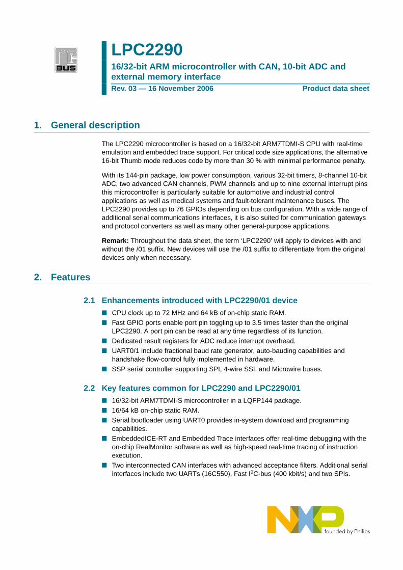
1. General description The LPC2290 microcontroller is based on a 16/32-bit ARM7TDMI-S CPU with real-time emulation and embedded trace support. For critical code size applications, the alternative 16-bit Thumb mode reduces code by more than 30 % with minimal performance penalty. With its 144-pin package, low power consumption, various 32-bit timers, 8-channel 10-bit ADC, two advanced CAN channels, PWM channels and up to nine external interrupt pins this microcontroller is particularly suitable for automotive and industrial control applications as well as medical systems and fault-tolerant maintenance buses. The LPC2290 provides up to 76 GPIOs depending on bus configuration. With a wide range of additional serial communications interfaces, it is also suited for communication gateways and protocol converters as well as many other general-purpose applications. Remark: Throughout the data sheet, the term ‘LPC2290’ will apply to devices with and without the /01 suffix. New devices will use the /01 suffix to differentiate from the original devices only when necessary. 2. Features 2.1 Enhancements introduced with LPC2290/01 device ■ CPU clock up to 72 MHz and 64 kB of on-chip static RAM. ■ Fast GPIO ports enable port pin toggling up to 3.5 times faster than the original LPC2290. A port pin can be read at any time regardless of its function. ■ Dedicated result registers for ADC reduce interrupt overhead. ■ UART0/1 include fractional baud rate generator, auto-bauding capabilities and handshake flow-control fully implemented in hardware. ■ SSP serial controller supporting SPI, 4-wire SSI, and Microwire buses. 2.2 Key features common for LPC2290 and LPC2290/01 ■ 16/32-bit ARM7TDMI-S microcontroller in a LQFP144 package. ■ 16/64 kB on-chip static RAM. ■ Serial bootloader using UART0 provides in-system download and programming capabilities. ■ EmbeddedICE-RT and Embedded Trace interfaces offer real-time debugging with the on-chip RealMonitor software as well as high-speed real-time tracing of instruction execution. ■ Two interconnected CAN interfaces with advanced acceptance filters. Additional serial interfaces include two UARTs (16C550), Fast I 2 C-bus (400 kbit/s) and two SPIs. LPC2290 16/32-bit ARM microcontroller with CAN, 10-bit ADC and external memory interface Rev. 03 — 16 November 2006 Product data sheet

Welcome message from author
This document is posted to help you gain knowledge. Please leave a comment to let me know what you think about it! Share it to your friends and learn new things together.
Transcript
1. General description
The LPC2290 microcontroller is based on a 16/32-bit ARM7TDMI-S CPU with real-timeemulation and embedded trace support. For critical code size applications, the alternative16-bit Thumb mode reduces code by more than 30 % with minimal performance penalty.
With its 144-pin package, low power consumption, various 32-bit timers, 8-channel 10-bitADC, two advanced CAN channels, PWM channels and up to nine external interrupt pinsthis microcontroller is particularly suitable for automotive and industrial controlapplications as well as medical systems and fault-tolerant maintenance buses. TheLPC2290 provides up to 76 GPIOs depending on bus configuration. With a wide range ofadditional serial communications interfaces, it is also suited for communication gatewaysand protocol converters as well as many other general-purpose applications.
Remark: Throughout the data sheet, the term ‘LPC2290’ will apply to devices with andwithout the /01 suffix. New devices will use the /01 suffix to differentiate from the originaldevices only when necessary.
2. Features
2.1 Enhancements introduced with LPC2290/01 devicen CPU clock up to 72 MHz and 64 kB of on-chip static RAM.
n Fast GPIO ports enable port pin toggling up to 3.5 times faster than the originalLPC2290. A port pin can be read at any time regardless of its function.
n Dedicated result registers for ADC reduce interrupt overhead.
n UART0/1 include fractional baud rate generator, auto-bauding capabilities andhandshake flow-control fully implemented in hardware.
n SSP serial controller supporting SPI, 4-wire SSI, and Microwire buses.
2.2 Key features common for LPC2290 and LPC2290/01n 16/32-bit ARM7TDMI-S microcontroller in a LQFP144 package.
n 16/64 kB on-chip static RAM.
n Serial bootloader using UART0 provides in-system download and programmingcapabilities.
n EmbeddedICE-RT and Embedded Trace interfaces offer real-time debugging with theon-chip RealMonitor software as well as high-speed real-time tracing of instructionexecution.
n Two interconnected CAN interfaces with advanced acceptance filters. Additional serialinterfaces include two UARTs (16C550), Fast I2C-bus (400 kbit/s) and two SPIs.
LPC229016/32-bit ARM microcontroller with CAN, 10-bit ADC andexternal memory interfaceRev. 03 — 16 November 2006 Product data sheet
NXP Semiconductors LPC229016/32-bit ARM microcontroller with external memory interface
n Eight channel 10-bit ADC with conversion time as low as 2.44 µs.
n Two 32-bit timers (with four capture and four compare channels), PWM unit (sixoutputs), Real-Time Clock (RTC) and watchdog.
n Vectored Interrupt Controller (VIC) with configurable priorities and vector addresses.
n Configurable external memory interface with up to four banks, each up to 16 MB and8/16/32-bit data width.
n Up to 76 general purpose I/O pins (5 V tolerant). Up to nine edge/level sensitiveexternal interrupt pins available.
n 60/72 MHz maximum CPU clock available from programmable on-chip PLL withsettling time of 100 µs.
n On-chip crystal oscillator with an operating range of 1 MHz to 30 MHz.
n Power saving modes include Idle and Power-down.
n Processor wake-up from Power-down mode via external interrupt.
n Individual enable/disable of peripheral functions for power optimization.
n Dual power supply:
u CPU operating voltage range of 1.65 V to 1.95 V (1.8 V ± 0.15 V).
u I/O power supply range of 3.0 V to 3.6 V (3.3 V ± 10 %) with 5 V tolerant I/O pads.
3. Ordering information
3.1 Ordering options
Table 1. Ordering information
Type number Package
Name Description Version
LPC2290FBD144 LQFP144 plastic low profile quad flat package;144 leads; body 20 × 20 × 1.4 mm
SOT486-1
LPC2290FBD144/01 LQFP144 plastic low profile quad flat package;144 leads; body 20 × 20 × 1.4 mm
SOT486-1
Table 2. Ordering options
Type number RAM CAN Enhancements Temperature range
LPC2290FBD144 16 kB 2 channels None −40 °C to +85 °C
LPC2290FBD144/01 64 kB 2 channels Higher CPU clock, moreon-chip SRAM, Fast I/Os,improved UARTs, added SSP,upgraded ADC
−40 °C to +85 °C
LPC2290_3 © NXP B.V. 2006. All rights reserved.
Product data sheet Rev. 03 — 16 November 2006 2 of 41
NXP Semiconductors LPC229016/32-bit ARM microcontroller with external memory interface
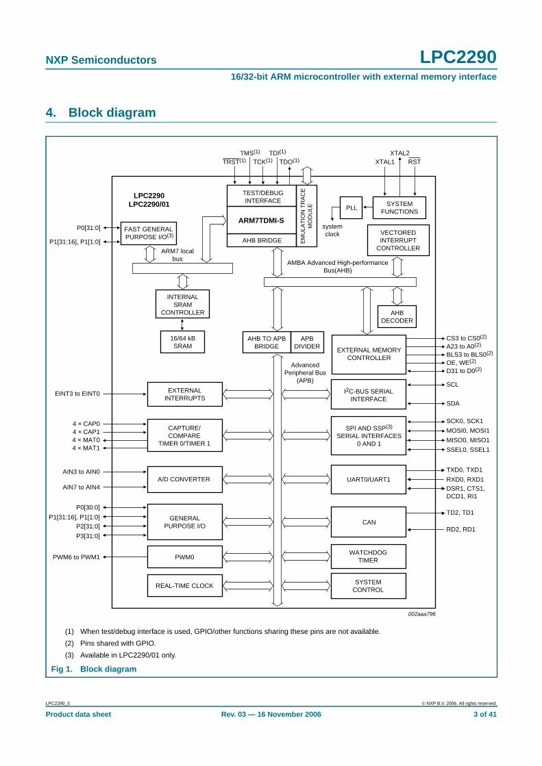
4. Block diagram
(1) When test/debug interface is used, GPIO/other functions sharing these pins are not available.
(2) Pins shared with GPIO.
(3) Available in LPC2290/01 only.
Fig 1. Block diagram
002aaa796
systemclock
SCL
P0[30:0]
P2[31:0]P1[31:16], P1[1:0]
P3[31:0]
SDA
CS3 to CS0(2)
A23 to A0(2)
BLS3 to BLS0(2)
OE, WE(2)
D31 to D0(2)
TRST(1)TMS(1)
TCK(1)TDI(1)
TDO(1)XTAL2
XTAL1
SCK0, SCK1
MOSI0, MOSI1
MISO0, MISO1
EINT3 to EINT0
4 × CAP04 × CAP1
4 × MAT14 × MAT0
AIN3 to AIN0
AIN7 to AIN4
PWM6 to PWM1
SSEL0, SSEL1
TD2, TD1
RD2, RD1
TXD0, TXD1
RXD0, RXD1DSR1, CTS1,DCD1, RI1
AMBA Advanced High-performanceBus(AHB)
AHB BRIDGE EM
ULA
TIO
N T
RA
CE
MO
DU
LE
TEST/DEBUGINTERFACE
AHBDECODER
AHB TO APBBRIDGE
APBDIVIDER
VECTOREDINTERRUPT
CONTROLLER
SYSTEMFUNCTIONS
PLL
SPI AND SSP(3)
SERIAL INTERFACES0 AND 1
I2C-BUS SERIALINTERFACE
UART0/UART1
CAN
WATCHDOGTIMER
SYSTEMCONTROL
EXTERNALINTERRUPTS
GENERALPURPOSE I/O
PWM0
CAPTURE/COMPARE
TIMER 0/TIMER 1
A/D CONVERTER
ARM7TDMI-S
LPC2290LPC2290/01
INTERNALSRAM
CONTROLLER
16/64 kBSRAM
ARM7 localbus
AdvancedPeripheral Bus
(APB)
REAL-TIME CLOCK
RST
EXTERNAL MEMORYCONTROLLER
P0[31:0]
P1[31:16], P1[1:0]
FAST GENERAL PURPOSE I/O(3)
LPC2290_3 © NXP B.V. 2006. All rights reserved.
Product data sheet Rev. 03 — 16 November 2006 3 of 41
NXP Semiconductors LPC229016/32-bit ARM microcontroller with external memory interface
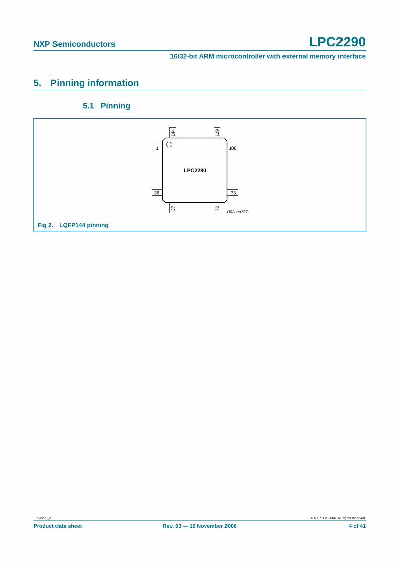
5. Pinning information
5.1 Pinning
Fig 2. LQFP144 pinning
LPC2290
108
37 72
144
109
73
1
36
002aaa797
LPC2290_3 © NXP B.V. 2006. All rights reserved.
Product data sheet Rev. 03 — 16 November 2006 4 of 41
NXP Semiconductors LPC229016/32-bit ARM microcontroller with external memory interface
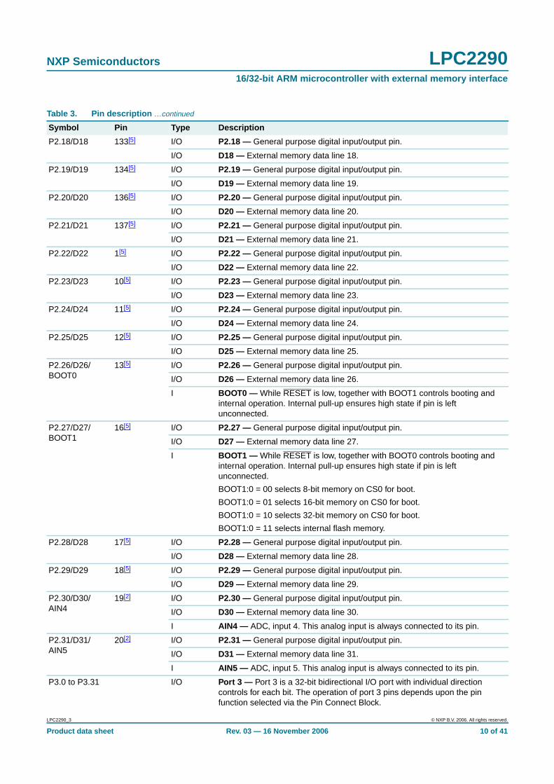
5.2 Pin description
Table 3. Pin description
Symbol Pin Type Description
P0.0 to P0.31 I/O Port 0: Port 0 is a 32-bit bidirectional I/O port with individual direction controlsfor each bit. The operation of port 0 pins depends upon the pin functionselected via the Pin Connect Block.
Pins 26 and 31 of port 0 are not available.
P0.0/TXD0/PWM1
42[1] I/O P0.0 — General purpose digital input/output pin.
O TXD0 — Transmitter output for UART0.
O PWM1 — Pulse Width Modulator output 1.
P0.1/RXD0/PWM3/EINT0
49[2] I/O P0.1 — General purpose digital input/output pin.
I RXD0 — Receiver input for UART0.
O PWM3 — Pulse Width Modulator output 3.
I EINT0 — External interrupt 0 input
P0.2/SCL/CAP0.0
50[3] I/O P0.2 — General purpose digital input/output pin.
I/O SCL — I2C-bus clock input/output. Open-drain output (for I2C-buscompliance).
I CAP0.0 — Capture input for Timer 0, channel 0.
P0.3/SDA/MAT0.0/EINT1
58[3] I/O P0.3 — General purpose digital input/output pin.
I/O SDA — I2C-bus data input/output. Open-drain output (for I2C-buscompliance).
O MAT0.0 — Match output for Timer 0, channel 0.
I EINT1 — External interrupt 1 input.
P0.4/SCK0/CAP0.1
59[1] I/O P0.4 — General purpose digital input/output pin.
I/O SCK0 — Serial clock for SPI0. SPI clock output from master or input to slave.
I CAP0.1 — Capture input for Timer 0, channel 1.
P0.5/MISO0/MAT0.1
61[1] I/O P0.5 — General purpose digital input/output pin.
I/O MISO0 — Master In Slave OUT for SPI0. Data input to SPI master or dataoutput from SPI slave.
O MAT0.1 — Match output for Timer 0, channel 1.
P0.6/MOSI0/CAP0.2
68[1] I/O P0.6 — General purpose digital input/output pin.
I/O MOSI0 — Master Out Slave In for SPI0. Data output from SPI master or datainput to SPI slave.
I CAP0.2 — Capture input for Timer 0, channel 2.
P0.7/SSEL0/PWM2/EINT2
69[2] I/O P0.7 — General purpose digital input/output pin.
I SSEL0 — Slave Select for SPI0. Selects the SPI interface as a slave.
O PWM2 — Pulse Width Modulator output 2.
I EINT2 — External interrupt 2 input.
P0.8/TXD1/PWM4
75[1] I/O P0.8 — General purpose digital input/output pin.
O TXD1 — Transmitter output for UART1.
O PWM4 — Pulse Width Modulator output 4.
LPC2290_3 © NXP B.V. 2006. All rights reserved.
Product data sheet Rev. 03 — 16 November 2006 5 of 41
NXP Semiconductors LPC229016/32-bit ARM microcontroller with external memory interface
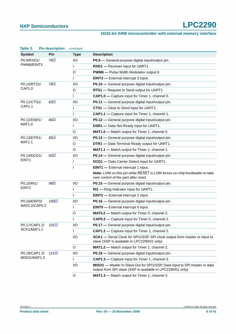
P0.9/RXD1/PWM6/EINT3
76[2] I/O P0.9 — General purpose digital input/output pin.
I RXD1 — Receiver input for UART1.
O PWM6 — Pulse Width Modulator output 6.
I EINT3 — External interrupt 3 input.
P0.10/RTS1/CAP1.0
78[1] I/O P0.10 — General purpose digital input/output pin.
O RTS1 — Request to Send output for UART1.
I CAP1.0 — Capture input for Timer 1, channel 0.
P0.11/CTS1/CAP1.1
83[1] I/O P0.11 — General purpose digital input/output pin.
I CTS1 — Clear to Send input for UART1.
I CAP1.1 — Capture input for Timer 1, channel 1.
P0.12/DSR1/MAT1.0
84[1] I/O P0.12 — General purpose digital input/output pin.
I DSR1 — Data Set Ready input for UART1.
O MAT1.0 — Match output for Timer 1, channel 0.
P0.13/DTR1/MAT1.1
85[1] I/O P0.13 — General purpose digital input/output pin.
O DTR1 — Data Terminal Ready output for UART1.
O MAT1.1 — Match output for Timer 1, channel 1.
P0.14/DCD1/EINT1
92[2] I/O P0.14 — General purpose digital input/output pin.
I DCD1 — Data Carrier Detect input for UART1.
I EINT1 — External interrupt 1 input.
Note: LOW on this pin while RESET is LOW forces on-chip bootloader to takeover control of the part after reset.
P0.15/RI1/EINT2
99[2] I/O P0.15 — General purpose digital input/output pin.
I RI1 — Ring Indicator input for UART1.
I EINT2 — External interrupt 2 input.
P0.16/EINT0/MAT0.2/CAP0.2
100[2] I/O P0.16 — General purpose digital input/output pin.
I EINT0 — External interrupt 0 input.
O MAT0.2 — Match output for Timer 0, channel 2.
I CAP0.2 — Capture input for Timer 0, channel 2.
P0.17/CAP1.2/SCK1/MAT1.2
101[1] I/O P0.17 — General purpose digital input/output pin.
I CAP1.2 — Capture input for Timer 1, channel 2.
I/O SCK1 — Serial Clock for SPI1/SSP. SPI clock output from master or input toslave (SSP is available in LPC2290/01 only).
O MAT1.2 — Match output for Timer 1, channel 2.
P0.18/CAP1.3/MISO1/MAT1.3
121[1] I/O P0.18 — General purpose digital input/output pin.
I CAP1.3 — Capture input for Timer 1, channel 3.
I/O MISO1 — Master In Slave Out for SPI1/SSP. Data input to SPI master or dataoutput from SPI slave (SSP is available in LPC2290/01 only).
O MAT1.3 — Match output for Timer 1, channel 3.
Table 3. Pin description …continued
Symbol Pin Type Description
LPC2290_3 © NXP B.V. 2006. All rights reserved.
Product data sheet Rev. 03 — 16 November 2006 6 of 41
NXP Semiconductors LPC229016/32-bit ARM microcontroller with external memory interface
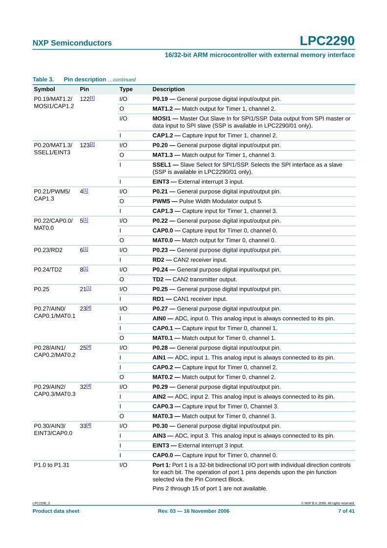
P0.19/MAT1.2/MOSI1/CAP1.2
122[1] I/O P0.19 — General purpose digital input/output pin.
O MAT1.2 — Match output for Timer 1, channel 2.
I/O MOSI1 — Master Out Slave In for SPI1/SSP. Data output from SPI master ordata input to SPI slave (SSP is available in LPC2290/01 only).
I CAP1.2 — Capture input for Timer 1, channel 2.
P0.20/MAT1.3/SSEL1/EINT3
123[2] I/O P0.20 — General purpose digital input/output pin.
O MAT1.3 — Match output for Timer 1, channel 3.
I SSEL1 — Slave Select for SPI1/SSP. Selects the SPI interface as a slave(SSP is available in LPC2290/01 only).
I EINT3 — External interrupt 3 input.
P0.21/PWM5/CAP1.3
4[1] I/O P0.21 — General purpose digital input/output pin.
O PWM5 — Pulse Width Modulator output 5.
I CAP1.3 — Capture input for Timer 1, channel 3.
P0.22/CAP0.0/MAT0.0
5[1] I/O P0.22 — General purpose digital input/output pin.
I CAP0.0 — Capture input for Timer 0, channel 0.
O MAT0.0 — Match output for Timer 0, channel 0.
P0.23/RD2 6[1] I/O P0.23 — General purpose digital input/output pin.
I RD2 — CAN2 receiver input.
P0.24/TD2 8[1] I/O P0.24 — General purpose digital input/output pin.
O TD2 — CAN2 transmitter output.
P0.25 21[1] I/O P0.25 — General purpose digital input/output pin.
I RD1 — CAN1 receiver input.
P0.27/AIN0/CAP0.1/MAT0.1
23[4] I/O P0.27 — General purpose digital input/output pin.
I AIN0 — ADC, input 0. This analog input is always connected to its pin.
I CAP0.1 — Capture input for Timer 0, channel 1.
O MAT0.1 — Match output for Timer 0, channel 1.
P0.28/AIN1/CAP0.2/MAT0.2
25[4] I/O P0.28 — General purpose digital input/output pin.
I AIN1 — ADC, input 1. This analog input is always connected to its pin.
I CAP0.2 — Capture input for Timer 0, channel 2.
O MAT0.2 — Match output for Timer 0, channel 2.
P0.29/AIN2/CAP0.3/MAT0.3
32[4] I/O P0.29 — General purpose digital input/output pin.
I AIN2 — ADC, input 2. This analog input is always connected to its pin.
I CAP0.3 — Capture input for Timer 0, Channel 3.
O MAT0.3 — Match output for Timer 0, channel 3.
P0.30/AIN3/EINT3/CAP0.0
33[4] I/O P0.30 — General purpose digital input/output pin.
I AIN3 — ADC, input 3. This analog input is always connected to its pin.
I EINT3 — External interrupt 3 input.
I CAP0.0 — Capture input for Timer 0, channel 0.
P1.0 to P1.31 I/O Port 1: Port 1 is a 32-bit bidirectional I/O port with individual direction controlsfor each bit. The operation of port 1 pins depends upon the pin functionselected via the Pin Connect Block.
Pins 2 through 15 of port 1 are not available.
Table 3. Pin description …continued
Symbol Pin Type Description
LPC2290_3 © NXP B.V. 2006. All rights reserved.
Product data sheet Rev. 03 — 16 November 2006 7 of 41
NXP Semiconductors LPC229016/32-bit ARM microcontroller with external memory interface
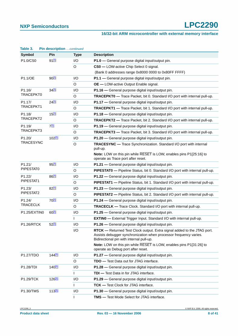
P1.0/CS0 91[5] I/O P1.0 — General purpose digital input/output pin.
O CS0 — LOW-active Chip Select 0 signal.
(Bank 0 addresses range 0x8000 0000 to 0x80FF FFFF)
P1.1/OE 90[5] I/O P1.1 — General purpose digital input/output pin.
O OE — LOW-active Output Enable signal.
P1.16/TRACEPKT0
34[5] I/O P1.16 — General purpose digital input/output pin.
O TRACEPKT0 — Trace Packet, bit 0. Standard I/O port with internal pull-up.
P1.17/TRACEPKT1
24[5] I/O P1.17 — General purpose digital input/output pin.
O TRACEPKT1 — Trace Packet, bit 1. Standard I/O port with internal pull-up.
P1.18/TRACEPKT2
15[5] I/O P1.18 — General purpose digital input/output pin.
O TRACEPKT2 — Trace Packet, bit 2. Standard I/O port with internal pull-up.
P1.19/TRACEPKT3
7[5] I/O P1.19 — General purpose digital input/output pin.
O TRACEPKT3 — Trace Packet, bit 3. Standard I/O port with internal pull-up.
P1.20/TRACESYNC
102[5] I/O P1.20 — General purpose digital input/output pin.
O TRACESYNC — Trace Synchronization. Standard I/O port with internalpull-up.
Note: LOW on this pin while RESET is LOW, enables pins P1[25:16] tooperate as Trace port after reset.
P1.21/PIPESTAT0
95[5] I/O P1.21 — General purpose digital input/output pin.
O PIPESTAT0 — Pipeline Status, bit 0. Standard I/O port with internal pull-up.
P1.22/PIPESTAT1
86[5] I/O P1.22 — General purpose digital input/output pin.
O PIPESTAT1 — Pipeline Status, bit 1. Standard I/O port with internal pull-up.
P1.23/PIPESTAT2
82[5] I/O P1.23 — General purpose digital input/output pin.
O PIPESTAT2 — Pipeline Status, bit 2. Standard I/O port with internal pull-up.
P1.24/TRACECLK
70[5] I/O P1.24 — General purpose digital input/output pin.
O TRACECLK — Trace Clock. Standard I/O port with internal pull-up.
P1.25/EXTIN0 60[5] I/O P1.25 — General purpose digital input/output pin.
I EXTIN0 — External Trigger Input. Standard I/O with internal pull-up.
P1.26/RTCK 52[5] I/O P1.26 — General purpose digital input/output pin.
I/O RTCK — Returned Test Clock output. Extra signal added to the JTAG port.Assists debugger synchronization when processor frequency varies.Bidirectional pin with internal pull-up.
Note: LOW on this pin while RESET is LOW, enables pins P1[31:26] tooperate as Debug port after reset.
P1.27/TDO 144[5] I/O P1.27 — General purpose digital input/output pin.
O TDO — Test Data out for JTAG interface.
P1.28/TDI 140[5] I/O P1.28 — General purpose digital input/output pin.
I TDI — Test Data in for JTAG interface.
P1.29/TCK 126[5] I/O P1.29 — General purpose digital input/output pin.
I TCK — Test Clock for JTAG interface.
P1.30/TMS 113[5] I/O P1.30 — General purpose digital input/output pin.
I TMS — Test Mode Select for JTAG interface.
Table 3. Pin description …continued
Symbol Pin Type Description
LPC2290_3 © NXP B.V. 2006. All rights reserved.
Product data sheet Rev. 03 — 16 November 2006 8 of 41
NXP Semiconductors LPC229016/32-bit ARM microcontroller with external memory interface
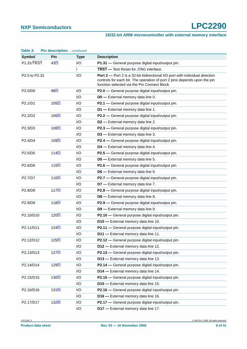
P1.31/TRST 43[5] I/O P1.31 — General purpose digital input/output pin.
I TRST — Test Reset for JTAG interface.
P2.0 to P2.31 I/O Port 2 — Port 2 is a 32-bit bidirectional I/O port with individual directioncontrols for each bit. The operation of port 2 pins depends upon the pinfunction selected via the Pin Connect Block.
P2.0/D0 98[5] I/O P2.0 — General purpose digital input/output pin.
I/O D0 — External memory data line 0.
P2.1/D1 105[5] I/O P2.1 — General purpose digital input/output pin.
I/O D1 — External memory data line 1.
P2.2/D2 106[5] I/O P2.2 — General purpose digital input/output pin.
I/O D2 — External memory data line 2.
P2.3/D3 108[5] I/O P2.3 — General purpose digital input/output pin.
I/O D3 — External memory data line 3.
P2.4/D4 109[5] I/O P2.4 — General purpose digital input/output pin.
I/O D4 — External memory data line 4.
P2.5/D5 114[5] I/O P2.5 — General purpose digital input/output pin.
I/O D5 — External memory data line 5.
P2.6/D6 115[5] I/O P2.6 — General purpose digital input/output pin.
I/O D6 — External memory data line 6.
P2.7/D7 116[5] I/O P2.7 — General purpose digital input/output pin.
I/O D7 — External memory data line 7.
P2.8/D8 117[5] I/O P2.8 — General purpose digital input/output pin.
I/O D8 — External memory data line 8.
P2.9/D9 118[5] I/O P2.9 — General purpose digital input/output pin.
I/O D9 — External memory data line 9.
P2.10/D10 120[5] I/O P2.10 — General purpose digital input/output pin.
I/O D10 — External memory data line 10.
P2.11/D11 124[5] I/O P2.11 — General purpose digital input/output pin.
I/O D11 — External memory data line 11.
P2.12/D12 125[5] I/O P2.12 — General purpose digital input/output pin.
I/O D12 — External memory data line 12.
P2.13/D13 127[5] I/O P2.13 — General purpose digital input/output pin.
I/O D13 — External memory data line 13.
P2.14/D14 129[5] I/O P2.14 — General purpose digital input/output pin.
I/O D14 — External memory data line 14.
P2.15/D15 130[5] I/O P2.15 — General purpose digital input/output pin.
I/O D15 — External memory data line 15.
P2.16/D16 131[5] I/O P2.16 — General purpose digital input/output pin.
I/O D16 — External memory data line 16.
P2.17/D17 132[5] I/O P2.17 — General purpose digital input/output pin.
I/O D17 — External memory data line 17.
Table 3. Pin description …continued
Symbol Pin Type Description
LPC2290_3 © NXP B.V. 2006. All rights reserved.
Product data sheet Rev. 03 — 16 November 2006 9 of 41
NXP Semiconductors LPC229016/32-bit ARM microcontroller with external memory interface
P2.18/D18 133[5] I/O P2.18 — General purpose digital input/output pin.
I/O D18 — External memory data line 18.
P2.19/D19 134[5] I/O P2.19 — General purpose digital input/output pin.
I/O D19 — External memory data line 19.
P2.20/D20 136[5] I/O P2.20 — General purpose digital input/output pin.
I/O D20 — External memory data line 20.
P2.21/D21 137[5] I/O P2.21 — General purpose digital input/output pin.
I/O D21 — External memory data line 21.
P2.22/D22 1[5] I/O P2.22 — General purpose digital input/output pin.
I/O D22 — External memory data line 22.
P2.23/D23 10[5] I/O P2.23 — General purpose digital input/output pin.
I/O D23 — External memory data line 23.
P2.24/D24 11[5] I/O P2.24 — General purpose digital input/output pin.
I/O D24 — External memory data line 24.
P2.25/D25 12[5] I/O P2.25 — General purpose digital input/output pin.
I/O D25 — External memory data line 25.
P2.26/D26/BOOT0
13[5] I/O P2.26 — General purpose digital input/output pin.
I/O D26 — External memory data line 26.
I BOOT0 — While RESET is low, together with BOOT1 controls booting andinternal operation. Internal pull-up ensures high state if pin is leftunconnected.
P2.27/D27/BOOT1
16[5] I/O P2.27 — General purpose digital input/output pin.
I/O D27 — External memory data line 27.
I BOOT1 — While RESET is low, together with BOOT0 controls booting andinternal operation. Internal pull-up ensures high state if pin is leftunconnected.
BOOT1:0 = 00 selects 8-bit memory on CS0 for boot.
BOOT1:0 = 01 selects 16-bit memory on CS0 for boot.
BOOT1:0 = 10 selects 32-bit memory on CS0 for boot.
BOOT1:0 = 11 selects internal flash memory.
P2.28/D28 17[5] I/O P2.28 — General purpose digital input/output pin.
I/O D28 — External memory data line 28.
P2.29/D29 18[5] I/O P2.29 — General purpose digital input/output pin.
I/O D29 — External memory data line 29.
P2.30/D30/AIN4
19[2] I/O P2.30 — General purpose digital input/output pin.
I/O D30 — External memory data line 30.
I AIN4 — ADC, input 4. This analog input is always connected to its pin.
P2.31/D31/AIN5
20[2] I/O P2.31 — General purpose digital input/output pin.
I/O D31 — External memory data line 31.
I AIN5 — ADC, input 5. This analog input is always connected to its pin.
P3.0 to P3.31 I/O Port 3 — Port 3 is a 32-bit bidirectional I/O port with individual directioncontrols for each bit. The operation of port 3 pins depends upon the pinfunction selected via the Pin Connect Block.
Table 3. Pin description …continued
Symbol Pin Type Description
LPC2290_3 © NXP B.V. 2006. All rights reserved.
Product data sheet Rev. 03 — 16 November 2006 10 of 41
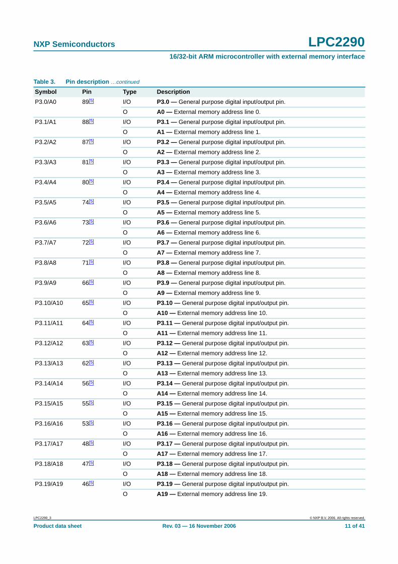
NXP Semiconductors LPC229016/32-bit ARM microcontroller with external memory interface
P3.0/A0 89[5] I/O P3.0 — General purpose digital input/output pin.
O A0 — External memory address line 0.
P3.1/A1 88[5] I/O P3.1 — General purpose digital input/output pin.
O A1 — External memory address line 1.
P3.2/A2 87[5] I/O P3.2 — General purpose digital input/output pin.
O A2 — External memory address line 2.
P3.3/A3 81[5] I/O P3.3 — General purpose digital input/output pin.
O A3 — External memory address line 3.
P3.4/A4 80[5] I/O P3.4 — General purpose digital input/output pin.
O A4 — External memory address line 4.
P3.5/A5 74[5] I/O P3.5 — General purpose digital input/output pin.
O A5 — External memory address line 5.
P3.6/A6 73[5] I/O P3.6 — General purpose digital input/output pin.
O A6 — External memory address line 6.
P3.7/A7 72[5] I/O P3.7 — General purpose digital input/output pin.
O A7 — External memory address line 7.
P3.8/A8 71[5] I/O P3.8 — General purpose digital input/output pin.
O A8 — External memory address line 8.
P3.9/A9 66[5] I/O P3.9 — General purpose digital input/output pin.
O A9 — External memory address line 9.
P3.10/A10 65[5] I/O P3.10 — General purpose digital input/output pin.
O A10 — External memory address line 10.
P3.11/A11 64[5] I/O P3.11 — General purpose digital input/output pin.
O A11 — External memory address line 11.
P3.12/A12 63[5] I/O P3.12 — General purpose digital input/output pin.
O A12 — External memory address line 12.
P3.13/A13 62[5] I/O P3.13 — General purpose digital input/output pin.
O A13 — External memory address line 13.
P3.14/A14 56[5] I/O P3.14 — General purpose digital input/output pin.
O A14 — External memory address line 14.
P3.15/A15 55[5] I/O P3.15 — General purpose digital input/output pin.
O A15 — External memory address line 15.
P3.16/A16 53[5] I/O P3.16 — General purpose digital input/output pin.
O A16 — External memory address line 16.
P3.17/A17 48[5] I/O P3.17 — General purpose digital input/output pin.
O A17 — External memory address line 17.
P3.18/A18 47[5] I/O P3.18 — General purpose digital input/output pin.
O A18 — External memory address line 18.
P3.19/A19 46[5] I/O P3.19 — General purpose digital input/output pin.
O A19 — External memory address line 19.
Table 3. Pin description …continued
Symbol Pin Type Description
LPC2290_3 © NXP B.V. 2006. All rights reserved.
Product data sheet Rev. 03 — 16 November 2006 11 of 41
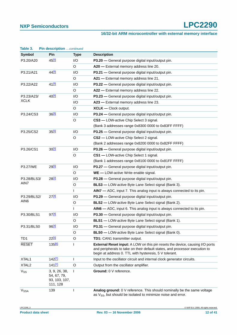
NXP Semiconductors LPC229016/32-bit ARM microcontroller with external memory interface
P3.20/A20 45[5] I/O P3.20 — General purpose digital input/output pin.
O A20 — External memory address line 20.
P3.21/A21 44[5] I/O P3.21 — General purpose digital input/output pin.
O A21 — External memory address line 21.
P3.22/A22 41[5] I/O P3.22 — General purpose digital input/output pin.
O A22 — External memory address line 22.
P3.23/A23/XCLK
40[5] I/O P3.23 — General purpose digital input/output pin.
I/O A23 — External memory address line 23.
O XCLK — Clock output.
P3.24/CS3 36[5] I/O P3.24 — General purpose digital input/output pin.
O CS3 — LOW-active Chip Select 3 signal.
(Bank 3 addresses range 0x8300 0000 to 0x83FF FFFF)
P3.25/CS2 35[5] I/O P3.25 — General purpose digital input/output pin.
O CS2 — LOW-active Chip Select 2 signal.
(Bank 2 addresses range 0x8200 0000 to 0x82FF FFFF)
P3.26/CS1 30[5] I/O P3.26 — General purpose digital input/output pin.
O CS1 — LOW-active Chip Select 1 signal.
(Bank 1 addresses range 0x8100 0000 to 0x81FF FFFF)
P3.27/WE 29[5] I/O P3.27 — General purpose digital input/output pin.
O WE — LOW-active Write enable signal.
P3.28/BLS3/AIN7
28[2] I/O P3.28 — General purpose digital input/output pin.
O BLS3 — LOW-active Byte Lane Select signal (Bank 3).
I AIN7 — ADC, input 7. This analog input is always connected to its pin.
P3.29/BLS2/AIN6
27[4] I/O P3.29 — General purpose digital input/output pin.
O BLS2 — LOW-active Byte Lane Select signal (Bank 2).
I AIN6 — ADC, input 6. This analog input is always connected to its pin.
P3.30/BLS1 97[4] I/O P3.30 — General purpose digital input/output pin.
O BLS1 — LOW-active Byte Lane Select signal (Bank 1).
P3.31/BLS0 96[4] I/O P3.31 — General purpose digital input/output pin.
O BLS0 — LOW-active Byte Lane Select signal (Bank 0).
TD1 22[5] O TD1: CAN1 transmitter output.
RESET 135[6] I External Reset input: A LOW on this pin resets the device, causing I/O portsand peripherals to take on their default states, and processor execution tobegin at address 0. TTL with hysteresis, 5 V tolerant.
XTAL1 142[7] I Input to the oscillator circuit and internal clock generator circuits.
XTAL2 141[7] O Output from the oscillator amplifier.
VSS 3, 9, 26, 38,54, 67, 79,93, 103, 107,111, 128
I Ground: 0 V reference.
VSSA 139 I Analog ground: 0 V reference. This should nominally be the same voltageas VSS, but should be isolated to minimize noise and error.
Table 3. Pin description …continued
Symbol Pin Type Description
LPC2290_3 © NXP B.V. 2006. All rights reserved.
Product data sheet Rev. 03 — 16 November 2006 12 of 41
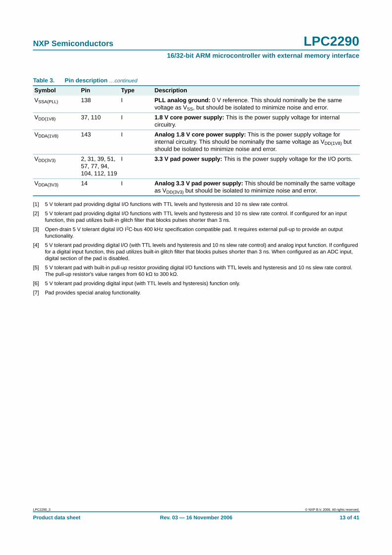
NXP Semiconductors LPC229016/32-bit ARM microcontroller with external memory interface
[1] 5 V tolerant pad providing digital I/O functions with TTL levels and hysteresis and 10 ns slew rate control.
[2] 5 V tolerant pad providing digital I/O functions with TTL levels and hysteresis and 10 ns slew rate control. If configured for an inputfunction, this pad utilizes built-in glitch filter that blocks pulses shorter than 3 ns.
[3] Open-drain 5 V tolerant digital I/O I2C-bus 400 kHz specification compatible pad. It requires external pull-up to provide an outputfunctionality.
[4] 5 V tolerant pad providing digital I/O (with TTL levels and hysteresis and 10 ns slew rate control) and analog input function. If configuredfor a digital input function, this pad utilizes built-in glitch filter that blocks pulses shorter than 3 ns. When configured as an ADC input,digital section of the pad is disabled.
[5] 5 V tolerant pad with built-in pull-up resistor providing digital I/O functions with TTL levels and hysteresis and 10 ns slew rate control.The pull-up resistor’s value ranges from 60 kΩ to 300 kΩ.
[6] 5 V tolerant pad providing digital input (with TTL levels and hysteresis) function only.
[7] Pad provides special analog functionality.
VSSA(PLL) 138 I PLL analog ground: 0 V reference. This should nominally be the samevoltage as VSS, but should be isolated to minimize noise and error.
VDD(1V8) 37, 110 I 1.8 V core power supply: This is the power supply voltage for internalcircuitry.
VDDA(1V8) 143 I Analog 1.8 V core power supply: This is the power supply voltage forinternal circuitry. This should be nominally the same voltage as VDD(1V8) butshould be isolated to minimize noise and error.
VDD(3V3) 2, 31, 39, 51,57, 77, 94,104, 112, 119
I 3.3 V pad power supply: This is the power supply voltage for the I/O ports.
VDDA(3V3) 14 I Analog 3.3 V pad power supply: This should be nominally the same voltageas VDD(3V3) but should be isolated to minimize noise and error.
Table 3. Pin description …continued
Symbol Pin Type Description
LPC2290_3 © NXP B.V. 2006. All rights reserved.
Product data sheet Rev. 03 — 16 November 2006 13 of 41
NXP Semiconductors LPC229016/32-bit ARM microcontroller with external memory interface
6. Functional description
6.1 Architectural overviewThe ARM7TDMI-S is a general purpose 32-bit microprocessor, which offers highperformance and very low power consumption. The ARM architecture is based on RISCprinciples, and the instruction set and related decode mechanism are much simpler thanthose of microprogrammed CISC. This simplicity results in a high instruction throughputand impressive real-time interrupt response from a small and cost-effective processorcore.
Pipeline techniques are employed so that all parts of the processing and memory systemscan operate continuously. Typically, while one instruction is being executed, its successoris being decoded, and a third instruction is being fetched from memory.
The ARM7TDMI-S processor also employs a unique architectural strategy known asThumb, which makes it ideally suited to high-volume applications with memoryrestrictions, or applications where code density is an issue.
The key idea behind Thumb is that of a super-reduced instruction set. Essentially, theARM7TDMI-S processor has two instruction sets:
• The standard 32-bit ARM set.
• A 16-bit Thumb set.
The Thumb set’s 16-bit instruction length allows it to approach twice the density ofstandard ARM code while retaining most of the ARM’s performance advantage over atraditional 16-bit processor using 16-bit registers. This is possible because Thumb codeoperates on the same 32-bit register set as ARM code.
Thumb code is able to provide up to 65 % of the code size of ARM, and 160 % of theperformance of an equivalent ARM processor connected to a 16-bit memory system.
6.2 On-chip SRAMOn-chip SRAM may be used for code and/or data storage. The SRAM may be accessedas 8-bit, 16-bit, and 32-bit. The LPC2290 provides 16 kB of SRAM and the LPC2290/01provides 64 kB of SRAM.
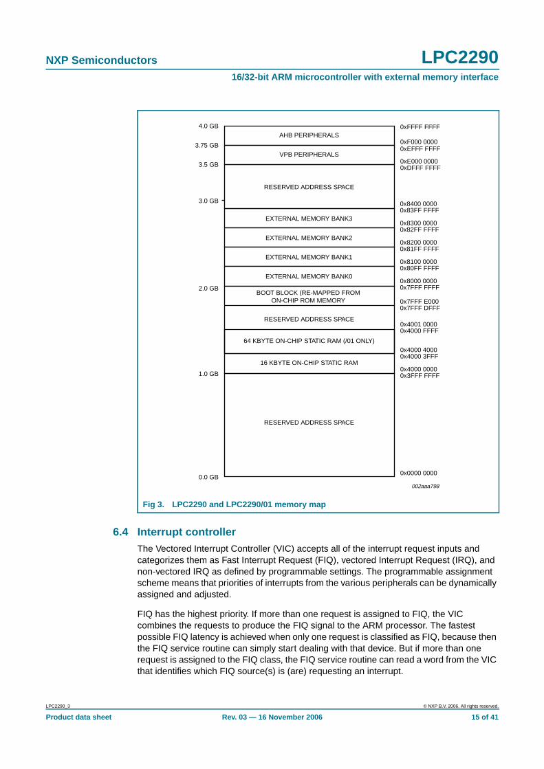
6.3 Memory mapThe LPC2290 memory maps incorporate several distinct regions, as shown in Figure 3.
In addition, the CPU interrupt vectors may be re-mapped to allow them to reside in eitheron-chip bootloader, external memory BANK0 or on-chip static RAM. This is described inSection 6.18 “System control”.
LPC2290_3 © NXP B.V. 2006. All rights reserved.
Product data sheet Rev. 03 — 16 November 2006 14 of 41
NXP Semiconductors LPC229016/32-bit ARM microcontroller with external memory interface
6.4 Interrupt controllerThe Vectored Interrupt Controller (VIC) accepts all of the interrupt request inputs andcategorizes them as Fast Interrupt Request (FIQ), vectored Interrupt Request (IRQ), andnon-vectored IRQ as defined by programmable settings. The programmable assignmentscheme means that priorities of interrupts from the various peripherals can be dynamicallyassigned and adjusted.
FIQ has the highest priority. If more than one request is assigned to FIQ, the VICcombines the requests to produce the FIQ signal to the ARM processor. The fastestpossible FIQ latency is achieved when only one request is classified as FIQ, because thenthe FIQ service routine can simply start dealing with that device. But if more than onerequest is assigned to the FIQ class, the FIQ service routine can read a word from the VICthat identifies which FIQ source(s) is (are) requesting an interrupt.
Fig 3. LPC2290 and LPC2290/01 memory map
AHB PERIPHERALS
VPB PERIPHERALS
RESERVED ADDRESS SPACE
RESERVED ADDRESS SPACE
16 KBYTE ON-CHIP STATIC RAM
64 KBYTE ON-CHIP STATIC RAM (/01 ONLY)
RESERVED ADDRESS SPACE
0xFFFF FFFF
0xF000 00000xEFFF FFFF
0xE000 00000xDFFF FFFF
0x4000 40000x4000 3FFF
0x4001 00000x4000 FFFF
0x4000 00000x3FFF FFFF
4.0 GB
3.75 GB
3.5 GB
3.0 GB
2.0 GB
1.0 GB
0.0 GB0x0000 0000
002aaa798
0x8400 0000
0x7FFF FFFF
EXTERNAL MEMORY BANK30x83FF FFFF
0x8300 0000
EXTERNAL MEMORY BANK20x82FF FFFF
0x8200 0000
EXTERNAL MEMORY BANK10x81FF FFFF
0x8100 0000
EXTERNAL MEMORY BANK00x80FF FFFF
0x8000 0000
BOOT BLOCK (RE-MAPPED FROMON-CHIP ROM MEMORY 0x7FFF E000
0x7FFF DFFF
LPC2290_3 © NXP B.V. 2006. All rights reserved.
Product data sheet Rev. 03 — 16 November 2006 15 of 41
NXP Semiconductors LPC229016/32-bit ARM microcontroller with external memory interface
Vectored IRQs have the middle priority. Sixteen of the interrupt requests can be assignedto this category. Any of the interrupt requests can be assigned to any of the 16 vectoredIRQ slots, among which slot 0 has the highest priority and slot 15 has the lowest.
Non-vectored IRQs have the lowest priority.
The VIC combines the requests from all the vectored and non-vectored IRQs to producethe IRQ signal to the ARM processor. The IRQ service routine can start by reading aregister from the VIC and jumping there. If any of the vectored IRQs are requesting, theVIC provides the address of the highest-priority requesting IRQs service routine,otherwise it provides the address of a default routine that is shared by all the non-vectoredIRQs. The default routine can read another VIC register to see what IRQs are active.
6.4.1 Interrupt sources
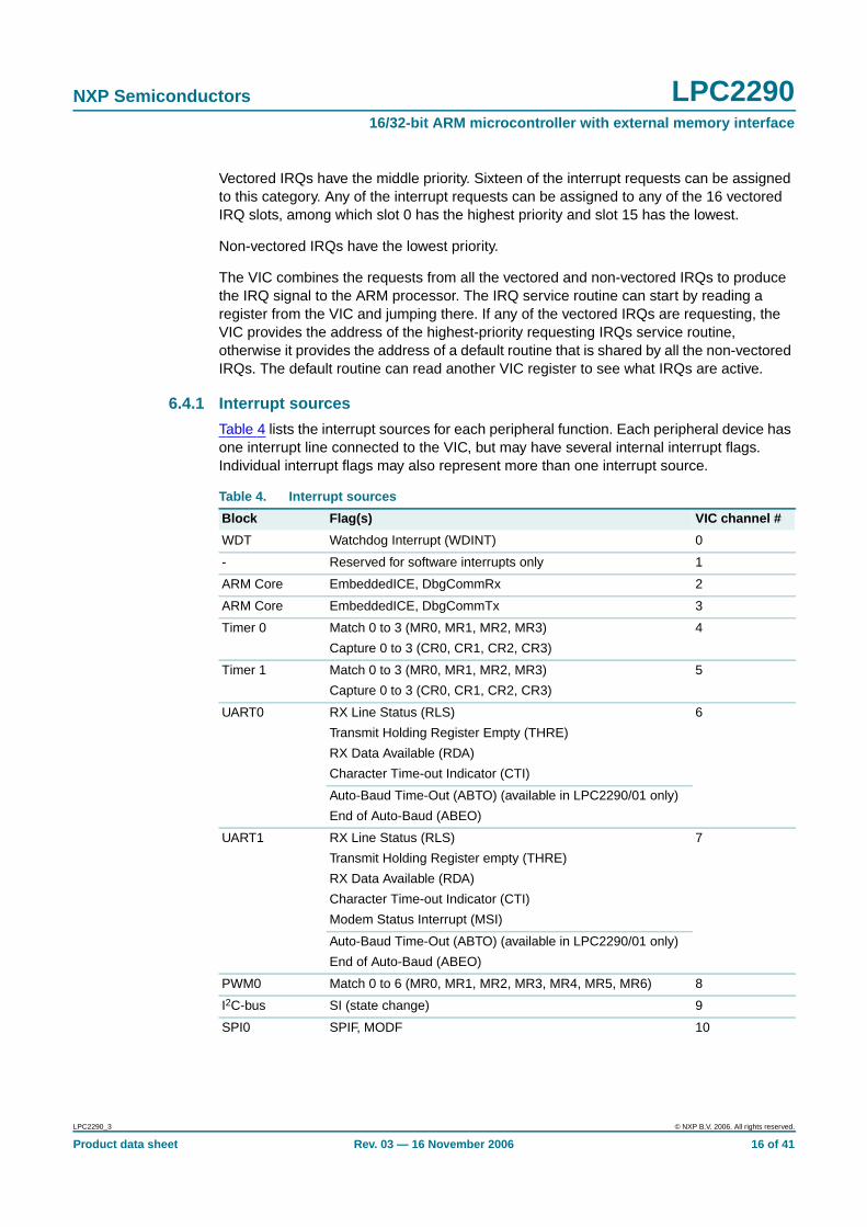
Table 4 lists the interrupt sources for each peripheral function. Each peripheral device hasone interrupt line connected to the VIC, but may have several internal interrupt flags.Individual interrupt flags may also represent more than one interrupt source.
Table 4. Interrupt sources
Block Flag(s) VIC channel #
WDT Watchdog Interrupt (WDINT) 0
- Reserved for software interrupts only 1
ARM Core EmbeddedICE, DbgCommRx 2
ARM Core EmbeddedICE, DbgCommTx 3
Timer 0 Match 0 to 3 (MR0, MR1, MR2, MR3)
Capture 0 to 3 (CR0, CR1, CR2, CR3)
4
Timer 1 Match 0 to 3 (MR0, MR1, MR2, MR3)
Capture 0 to 3 (CR0, CR1, CR2, CR3)
5
UART0 RX Line Status (RLS)
Transmit Holding Register Empty (THRE)
RX Data Available (RDA)
Character Time-out Indicator (CTI)
6
Auto-Baud Time-Out (ABTO) (available in LPC2290/01 only)
End of Auto-Baud (ABEO)
UART1 RX Line Status (RLS)
Transmit Holding Register empty (THRE)
RX Data Available (RDA)
Character Time-out Indicator (CTI)
Modem Status Interrupt (MSI)
7
Auto-Baud Time-Out (ABTO) (available in LPC2290/01 only)
End of Auto-Baud (ABEO)
PWM0 Match 0 to 6 (MR0, MR1, MR2, MR3, MR4, MR5, MR6) 8
I2C-bus SI (state change) 9
SPI0 SPIF, MODF 10
LPC2290_3 © NXP B.V. 2006. All rights reserved.
Product data sheet Rev. 03 — 16 November 2006 16 of 41
NXP Semiconductors LPC229016/32-bit ARM microcontroller with external memory interface
6.5 Pin connect blockThe pin connect block allows selected pins of the microcontroller to have more than onefunction. Configuration registers control the multiplexers to allow connection between thepin and the on-chip peripherals. Peripherals should be connected to the appropriate pinsprior to being activated, and prior to any related interrupt(s) being enabled. Activity of anyenabled peripheral function that is not mapped to a related pin should be consideredundefined.
6.6 External memory controllerThe external Static Memory Controller is a module which provides an interface betweenthe system bus and external (off-chip) memory devices. It provides support for up to fourindependently configurable memory banks (16 MB each with byte lane enable control)simultaneously. Each memory bank is capable of supporting SRAM, ROM, flash EPROM,burst ROM memory, or some external I/O devices.
Each memory bank may be 8-bit, 16-bit, or 32-bit wide.
6.7 General purpose parallel I/O and Fast I/ODevice pins that are not connected to a specific peripheral function are controlled by theGPIO registers. Pins may be dynamically configured as inputs or outputs. Separateregisters allow setting or clearing any number of outputs simultaneously. The value of theoutput register may be read back, as well as the current state of the port pins.
6.7.1 Features
• Direction control of individual bits.
• Separate control of output set and clear.
SPI1/SSP Source: SPI1 SPI Interrupt Flag (SPIF), Mode Fault (MODF) 11
Source: SSP (available in LPC2290/01 only)
TX FIFO at least half empty (TXRIS)
RX FIFO at least half full (RXRIS)
Receive Timeout condition (RTRIS)
Receive Overrun (RORRIS)
PLL PLL Lock (PLOCK) 12
RTC RTCCIF (Counter Increment), RTCALF (Alarm) 13
System Control External Interrupt 0 (EINT0) 14
External Interrupt 1 (EINT1) 15
External Interrupt 2 (EINT2) 16
External Interrupt 3 (EINT3) 17
A/D ADC 18
CAN 1 ORed CAN Acceptance Filter 19
CAN1 (TX int, RX int) 20, 21
CAN2 (TX int, RX int) 22, 23
Table 4. Interrupt sources …continued
Block Flag(s) VIC channel #
LPC2290_3 © NXP B.V. 2006. All rights reserved.
Product data sheet Rev. 03 — 16 November 2006 17 of 41
NXP Semiconductors LPC229016/32-bit ARM microcontroller with external memory interface
• All I/O default to inputs after reset.
6.7.2 Fast I/O features available in LPC2290/01 only
• Fast I/O registers are located on the ARM local bus for the fastest possible I/O timing.
• All GPIO registers are byte addressable.
• Entire port value can be written in one instruction.
• Mask registers allow single instruction to set or clear any number of bits in one port.
6.8 10-bit ADCThe LPC2290 each contain a single 10-bit successive approximation ADC with eightmultiplexed channels.
6.8.1 Features
• Measurement range of 0 V to 3.3 V.
• Capable of performing more than 400000 10-bit samples per second.
• Burst conversion mode for single or multiple inputs.
• Optional conversion on transition on input pin or Timer Match signal.
6.8.2 ADC features available in LPC2290/01 only
• Every analog input has a dedicated result register to reduce interrupt overhead.
• Every analog input can generate an interrupt once the conversion is completed.
6.9 CAN controllers and acceptance filterThe LPC2290 contains two CAN controllers. The CAN is a serial communications protocolwhich efficiently supports distributed real-time control with a very high level of security. Itsdomain of application ranges from high-speed networks to low cost multiplex wiring.
6.9.1 Features
• Data rates up to 1 Mbit/s on each bus.
• 32-bit register and RAM access.
• Compatible with CAN specification 2.0B, ISO 11898-1.
• Global Acceptance Filter recognizes 11-bit and 29-bit RX identifiers for all CAN buses.
• Acceptance Filter can provide FullCAN-style automatic reception for selectedStandard identifiers.
• Full CAN messages can generate interrupts.
6.10 UARTsThe LPC2290 contains two UARTs. In addition to standard transmit and receive datalines, UART1 also provides a full modem control handshake interface.
6.10.1 Features
• 16 B Receive and Transmit FIFOs.
LPC2290_3 © NXP B.V. 2006. All rights reserved.
Product data sheet Rev. 03 — 16 November 2006 18 of 41
NXP Semiconductors LPC229016/32-bit ARM microcontroller with external memory interface
• Register locations conform to 16C550 industry standard.
• Receiver FIFO trigger points at 1 B, 4 B, 8 B, and 14 B.
• Built-in baud rate generator.
• Standard modem interface signals included on UART1.
6.10.2 UART features available in LPC2290/01 only
• The transmission FIFO control enables implementation of software (XON/XOFF) flowcontrol on both UARTs and hardware (CTS/RTS) flow control on UART1 only.
• Fractional baud rate generator enables standard baud rates such as 115200 to beachieved with any crystal frequency above 2 MHz.
• Auto-bauding.
• Auto-CTS/RTS flow-control fully implemented in hardware.
6.11 I2C-bus serial I/O controllerThe I2C-bus is bidirectional, for inter-IC control using only two wires: a serial clock line(SCL), and a serial data line (SDA). Each device is recognized by a unique address andcan operate as either a receiver-only device (e.g., an LCD driver or a transmitter with thecapability to both receive and send information (such as memory). Transmitters and/orreceivers can operate in either master or slave mode, depending on whether the chip hasto initiate a data transfer or is only addressed. The I2C-bus is a multi-master bus, it can becontrolled by more than one bus master connected to it.
The I2C-bus implemented in LPC2290 supports bit rate up to 400 kbit/s (Fast I2C-bus).
6.11.1 Features
• Compliant with standard I2C-bus interface.
• Easy to configure as master, slave, or master/slave.
• Programmable clocks allow versatile rate control.
• Bidirectional data transfer between masters and slaves.
• Multi-master bus (no central master).
• Arbitration between simultaneously transmitting masters without corruption of serialdata on the bus.
• Serial clock synchronization allows devices with different bit rates to communicate viaone serial bus.
• Serial clock synchronization can be used as a handshake mechanism to suspend andresume serial transfer.
• The I2C-bus may be used for test and diagnostic purposes.
6.12 SPI serial I/O controllerThe LPC2290 contains two SPIs. The SPI is a full duplex serial interface, designed to beable to handle multiple masters and slaves connected to a given bus. Only a single masterand a single slave can communicate on the interface during a given data transfer. During adata transfer the master always sends a byte of data to the slave, and the slave alwayssends a byte of data to the master.
LPC2290_3 © NXP B.V. 2006. All rights reserved.
Product data sheet Rev. 03 — 16 November 2006 19 of 41
NXP Semiconductors LPC229016/32-bit ARM microcontroller with external memory interface
6.12.1 Features
• Compliant with SPI specification.
• Synchronous, serial, full duplex, communication.
• Combined SPI master and slave.
• Maximum data bit rate of one eighth of the input clock rate.
6.13 SSP serial I/O controller (available in LPC2290/01 only)The LPC2290/01 contains one Serial Synchronous Port controller (SSP). The SSPcontroller is capable of operation on a SPI, 4-wire SSI, or Microwire bus. It can interactwith multiple masters and slaves on the bus. However, only a single master and a singleslave can communicate on the bus during a given data transfer. The SSP supports fullduplex transfers, with frames of 4 bits to 16 bits of data flowing from the master to theslave and from the slave to the master. Often only one of these data flows carriesmeaningful data.
The SSP and SPI1 share the same pins on LPC2290/01. After a reset, SPI1 is enabledand SSP is disabled.
6.13.1 Features
• Synchronous Serial Communication.
• 8-frame FIFOs for both transmit and receive.
• Compatible with Motorola SPI, 4-wire TI SSI and National Semiconductor Microwirebuses.
• Master or slave operation.
• Four bits to 16 bits per SPI frame.
6.14 General purpose timersThe TIMER0 and TIMER1 are designed to count cycles of the peripheral clock (PCLK)and optionally generate interrupts or perform other actions at specified timer values,based on four match registers. It also includes four capture inputs to trap the timer valuewhen an input signal transitions, optionally generating an interrupt. Multiple pins can beselected to perform a single capture or match function, providing an application with ‘or’and ‘and’, as well as ‘broadcast’ functions among them.
6.14.1 Features
• A 32-bit Timer/Counter with a programmable 32-bit prescaler.
• Four 32-bit capture channels per timer that can take a snapshot of the timer valuewhen an input signal transitions. A capture event may also optionally generate aninterrupt.
• Four 32-bit match registers that allow:
– Continuous operation with optional interrupt generation on match.
– Stop timer on match with optional interrupt generation.
– Reset timer on match with optional interrupt generation.
LPC2290_3 © NXP B.V. 2006. All rights reserved.
Product data sheet Rev. 03 — 16 November 2006 20 of 41
NXP Semiconductors LPC229016/32-bit ARM microcontroller with external memory interface
• Four external outputs per timer corresponding to match registers, with the followingcapabilities:
– Set LOW on match.
– Set HIGH on match.
– Toggle on match.
– Do nothing on match.
6.14.2 Timer features available in LPC2290/01 only
• Timers can count cycles of the externally supplied clock providing external eventcounting functionality
6.15 Watchdog timerThe purpose of the watchdog is to reset the microcontroller within a reasonable amount oftime if it enters an erroneous state. When enabled, the watchdog will generate a systemreset if the user program fails to ‘feed’ (or reload) the watchdog within a predeterminedamount of time.
6.15.1 Features
• Internally resets chip if not periodically reloaded.
• Debug mode.
• Enabled by software but requires a hardware reset or a watchdog reset/interrupt to bedisabled.
• Incorrect/incomplete feed sequence causes reset/interrupt if enabled.
• Flag to indicate watchdog reset.
• Programmable 32-bit timer with internal pre-scaler.
• Selectable time period from (Tcy(PCLK) × 256 × 4) to (Tcy(PCLK) × 232 × 4) in multiples ofTcy(PCLK) × 4.
6.16 Real-time clockThe Real-Time Clock (RTC) is designed to provide a set of counters to measure timewhen normal or idle operating mode is selected. The RTC has been designed to use littlepower, making it suitable for battery powered systems where the CPU is not runningcontinuously (Idle mode).
6.16.1 Features
• Measures the passage of time to maintain a calendar and clock.
• Ultra-low power design to support battery powered systems.
• Provides Seconds, Minutes, Hours, Day of Month, Month, Year, Day of Week, and Dayof Year.
• Programmable Reference Clock Divider allows adjustment of the RTC to matchvarious crystal frequencies.
LPC2290_3 © NXP B.V. 2006. All rights reserved.
Product data sheet Rev. 03 — 16 November 2006 21 of 41
NXP Semiconductors LPC229016/32-bit ARM microcontroller with external memory interface
6.17 Pulse width modulatorThe PWM is based on the standard Timer block and inherits all of its features, althoughonly the PWM function is pinned out on the LPC2290. The Timer is designed to countcycles of the peripheral clock (PCLK) and optionally generate interrupts or perform otheractions when specified timer values occur, based on seven match registers. The PWMfunction is also based on match register events.
The ability to separately control rising and falling edge locations allows the PWM to beused for more applications. For instance, multi-phase motor control typically requires threenon-overlapping PWM outputs with individual control of all three pulse widths andpositions.
Two match registers can be used to provide a single edge controlled PWM output. Onematch register (MR0) controls the PWM cycle rate, by resetting the count upon match.The other match register controls the PWM edge position. Additional single edgecontrolled PWM outputs require only one match register each, since the repetition rate isthe same for all PWM outputs. Multiple single edge controlled PWM outputs will all have arising edge at the beginning of each PWM cycle, when an MR0 match occurs.
Three match registers can be used to provide a PWM output with both edges controlled.Again, the MR0 match register controls the PWM cycle rate. The other match registerscontrol the two PWM edge positions. Additional double edge controlled PWM outputsrequire only two match registers each, since the repetition rate is the same for all PWMoutputs.
With double edge controlled PWM outputs, specific match registers control the rising andfalling edge of the output. This allows both positive going PWM pulses (when the risingedge occurs prior to the falling edge), and negative going PWM pulses (when the fallingedge occurs prior to the rising edge).
6.17.1 Features
• Seven match registers allow up to six single edge controlled or three double edgecontrolled PWM outputs, or a mix of both types.
• The match registers also allow:
– Continuous operation with optional interrupt generation on match.
– Stop timer on match with optional interrupt generation.
– Reset timer on match with optional interrupt generation.
• Supports single edge controlled and/or double edge controlled PWM outputs. Singleedge controlled PWM outputs all go HIGH at the beginning of each cycle unless theoutput is a constant LOW. Double edge controlled PWM outputs can have either edgeoccur at any position within a cycle. This allows for both positive going and negativegoing pulses.
• Pulse period and width can be any number of timer counts. This allows completeflexibility in the trade-off between resolution and repetition rate. All PWM outputs willoccur at the same repetition rate.
• Double edge controlled PWM outputs can be programmed to be either positive goingor negative going pulses.
LPC2290_3 © NXP B.V. 2006. All rights reserved.
Product data sheet Rev. 03 — 16 November 2006 22 of 41
NXP Semiconductors LPC229016/32-bit ARM microcontroller with external memory interface
• Match register updates are synchronized with pulse outputs to prevent generation oferroneous pulses. Software must ‘release’ new match values before they can becomeeffective.
• May be used as a standard timer if the PWM mode is not enabled.
• A 32-bit Timer/Counter with a programmable 32-bit prescaler.
6.18 System control
6.18.1 Crystal oscillator
The oscillator supports crystals in the range of 1 MHz to 30 MHz. The oscillator outputfrequency is called fosc and the ARM processor clock frequency is referred to as CCLK forpurposes of rate equations, etc. fosc and CCLK are the same value unless the PLL isrunning and connected. Refer to Section 6.18.2 “PLL” for additional information.
6.18.2 PLL
The PLL accepts an input clock frequency in the range of 10 MHz to 25 MHz. The inputfrequency is multiplied up into the range of 10 MHz to 60 MHz with a Current ControlledOscillator (CCO). The multiplier can be an integer value from 1 to 32 (in practice, themultiplier value cannot be higher than 6 on this family of microcontrollers due to the upperfrequency limit of the CPU). The CCO operates in the range of 156 MHz to 320 MHz, sothere is an additional divider in the loop to keep the CCO within its frequency range whilethe PLL is providing the desired output frequency. The output divider may be set to divideby 2, 4, 8, or 16 to produce the output clock. Since the minimum output divider value is 2,it is insured that the PLL output has a 50 % duty cycle.The PLL is turned off and bypassedfollowing a chip reset and may be enabled by software. The program must configure andactivate the PLL, wait for the PLL to Lock, then connect to the PLL as a clock source. ThePLL settling time is 100 µs.
6.18.3 Reset and wake-up timer
Reset has two sources on the LPC2290: the RESET pin and watchdog reset. The RESETpin is a Schmitt trigger input pin with an additional glitch filter. Assertion of chip reset byany source starts the Wake-up Timer (see Wake-up Timer description below), causing theinternal chip reset to remain asserted until the external reset is de-asserted, the oscillatoris running, a fixed number of clocks have passed, and the on-chip flash controller hascompleted its initialization.
When the internal reset is removed, the processor begins executing at address 0, which isthe reset vector. At that point, all of the processor and peripheral registers have beeninitialized to predetermined values.
The Wake-up Timer ensures that the oscillator and other analog functions required forchip operation are fully functional before the processor is allowed to execute instructions.This is important at power-on, all types of reset, and whenever any of the aforementionedfunctions are turned off for any reason. Since the oscillator and other functions are turnedoff during Power-down mode, any wake-up of the processor from Power-down modemakes use of the Wake-up Timer.
LPC2290_3 © NXP B.V. 2006. All rights reserved.
Product data sheet Rev. 03 — 16 November 2006 23 of 41
NXP Semiconductors LPC229016/32-bit ARM microcontroller with external memory interface
The Wake-up Timer monitors the crystal oscillator as the means of checking whether it issafe to begin code execution. When power is applied to the chip, or some event causedthe chip to exit Power-down mode, some time is required for the oscillator to produce asignal of sufficient amplitude to drive the clock logic. The amount of time depends onmany factors, including the rate of VDD ramp (in the case of power-on), the type of crystaland its electrical characteristics (if a quartz crystal is used), as well as any other externalcircuitry (e.g. capacitors), and the characteristics of the oscillator itself under the existingambient conditions.
6.18.4 External interrupt inputs
The LPC2290 include up to nine edge or level sensitive External Interrupt Inputs asselectable pin functions. When the pins are combined, external events can be processedas four independent interrupt signals. The External Interrupt Inputs can optionally be usedto wake up the processor from Power-down mode.
6.18.5 Memory mapping control
The Memory Mapping Control alters the mapping of the interrupt vectors that appearbeginning at address 0x0000 0000. Vectors may be mapped to the bottom of the on-chipflash memory, or to the on-chip static RAM. This allows code running in different memoryspaces to have control of the interrupts.
6.18.6 Power control
The LPC2290 support two reduced power modes: Idle mode and Power-down mode. InIdle mode, execution of instructions is suspended until either a reset or interrupt occurs.Peripheral functions continue operation during Idle mode and may generate interrupts tocause the processor to resume execution. Idle mode eliminates power used by theprocessor itself, memory systems and related controllers, and internal buses.
In Power-down mode, the oscillator is shut down and the chip receives no internal clocks.The processor state and registers, peripheral registers, and internal SRAM values arepreserved throughout Power-down mode and the logic levels of chip output pins remainstatic. The Power-down mode can be terminated and normal operation resumed by eithera reset or certain specific interrupts that are able to function without clocks. Since alldynamic operation of the chip is suspended, Power-down mode reduces chip powerconsumption to nearly zero.
A Power Control for Peripherals feature allows individual peripherals to be turned off ifthey are not needed in the application, resulting in additional power savings.
6.18.7 APB bus
The APB divider determines the relationship between the processor clock (CCLK) and theclock used by peripheral devices (PCLK). The APB divider serves two purposes. The firstis to provide peripherals with the desired PCLK via APB bus so that they can operate atthe speed chosen for the ARM processor. In order to achieve this, the APB bus may beslowed down to 1⁄2 to 1⁄4 of the processor clock rate. Because the APB bus must workproperly at power-up (and its timing cannot be altered if it does not work since the APBdivider control registers reside on the APB bus), the default condition at reset is for theAPB bus to run at 1⁄4 of the processor clock rate. The second purpose of the APB divideris to allow power savings when an application does not require any peripherals to run atthe full processor rate. Because the APB divider is connected to the PLL output, the PLLremains active (if it was running) during Idle mode.
LPC2290_3 © NXP B.V. 2006. All rights reserved.
Product data sheet Rev. 03 — 16 November 2006 24 of 41
NXP Semiconductors LPC229016/32-bit ARM microcontroller with external memory interface
6.19 Emulation and debuggingThe LPC2290 support emulation and debugging via a JTAG serial port. A trace portallows tracing program execution. Debugging and trace functions are multiplexed only withGPIOs on Port 1. This means that all communication, timer and interface peripheralsresiding on Port 0 are available during the development and debugging phase as they arewhen the application is run in the embedded system itself.
6.19.1 EmbeddedICE
Standard ARM EmbeddedICE logic provides on-chip debug support. The debugging ofthe target system requires a host computer running the debugger software and anEmbeddedICE protocol convertor. EmbeddedICE protocol convertor converts the remotedebug protocol commands to the JTAG data needed to access the ARM core.
The ARM core has a Debug Communication Channel function built-in. The debugcommunication channel allows a program running on the target to communicate with thehost debugger or another separate host without stopping the program flow or evenentering the debug state. The debug communication channel is accessed as acoprocessor 14 by the program running on the ARM7TDMI-S core. The debugcommunication channel allows the JTAG port to be used for sending and receiving datawithout affecting the normal program flow. The debug communication channel data andcontrol registers are mapped in to addresses in the EmbeddedICE logic.
6.19.2 Embedded trace
Since the LPC2290 has significant amounts of on-chip memory, it is not possible todetermine how the processor core is operating simply by observing the external pins. TheEmbedded Trace Macrocell (ETM) provides real-time trace capability for deeplyembedded processor cores. It outputs information about processor execution to the traceport.
The ETM is connected directly to the ARM core and not to the main AMBA system bus. Itcompresses the trace information and exports it through a narrow trace port. An externaltrace port analyzer must capture the trace information under software debugger control.Instruction trace (or PC trace) shows the flow of execution of the processor and provides alist of all the instructions that were executed. Instruction trace is significantly compressedby only broadcasting branch addresses as well as a set of status signals that indicate thepipeline status on a cycle by cycle basis. Trace information generation can be controlledby selecting the trigger resource. Trigger resources include address comparators,counters and sequencers. Since trace information is compressed the software debuggerrequires a static image of the code being executed. Self-modifying code can not be tracedbecause of this restriction.
6.19.3 RealMonitor
RealMonitor is a configurable software module, developed by ARM Inc., which enablesreal-time debug. It is a lightweight debug monitor that runs in the background while usersdebug their foreground application. It communicates with the host using the DCC (DebugCommunications Channel), which is present in the EmbeddedICE logic. The LPC2290contain a specific configuration of RealMonitor software programmed into the on-chipflash memory.
LPC2290_3 © NXP B.V. 2006. All rights reserved.
Product data sheet Rev. 03 — 16 November 2006 25 of 41
NXP Semiconductors LPC229016/32-bit ARM microcontroller with external memory interface
7. Limiting values
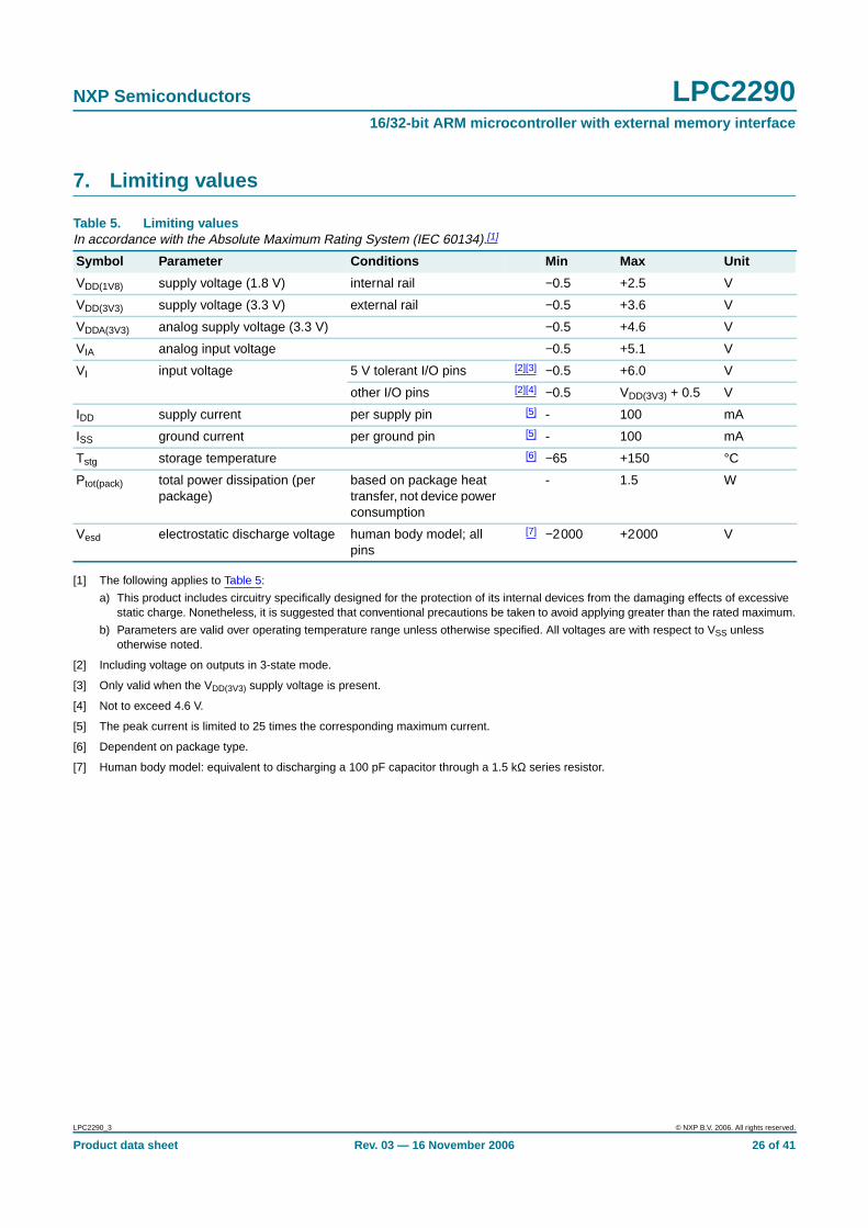
[1] The following applies to Table 5:
a) This product includes circuitry specifically designed for the protection of its internal devices from the damaging effects of excessivestatic charge. Nonetheless, it is suggested that conventional precautions be taken to avoid applying greater than the rated maximum.
b) Parameters are valid over operating temperature range unless otherwise specified. All voltages are with respect to VSS unlessotherwise noted.
[2] Including voltage on outputs in 3-state mode.
[3] Only valid when the VDD(3V3) supply voltage is present.
[4] Not to exceed 4.6 V.
[5] The peak current is limited to 25 times the corresponding maximum current.
[6] Dependent on package type.
[7] Human body model: equivalent to discharging a 100 pF capacitor through a 1.5 kΩ series resistor.
Table 5. Limiting valuesIn accordance with the Absolute Maximum Rating System (IEC 60134).[1]
Symbol Parameter Conditions Min Max Unit
VDD(1V8) supply voltage (1.8 V) internal rail −0.5 +2.5 V
VDD(3V3) supply voltage (3.3 V) external rail −0.5 +3.6 V
VDDA(3V3) analog supply voltage (3.3 V) −0.5 +4.6 V
VIA analog input voltage −0.5 +5.1 V
VI input voltage 5 V tolerant I/O pins [2][3] −0.5 +6.0 V
other I/O pins [2][4] −0.5 VDD(3V3) + 0.5 V
IDD supply current per supply pin [5] - 100 mA
ISS ground current per ground pin [5] - 100 mA
Tstg storage temperature [6] −65 +150 °C
Ptot(pack) total power dissipation (perpackage)
based on package heattransfer, not device powerconsumption
- 1.5 W
Vesd electrostatic discharge voltage human body model; allpins
[7] −2000 +2000 V
LPC2290_3 © NXP B.V. 2006. All rights reserved.
Product data sheet Rev. 03 — 16 November 2006 26 of 41
NXP Semiconductors LPC229016/32-bit ARM microcontroller with external memory interface
8. Static characteristics
Table 6. Static characteristicsTamb = −40 °C to +85 °C for industrial applications, unless otherwise specified.
Symbol Parameter Conditions Min Typ[1] Max Unit
VDD(1V8) supply voltage (1.8 V) internal rail 1.65 1.8 1.95 V
VDD(3V3) supply voltage (3.3 V) external rail 3.0 3.3 3.6 V
VDDA(3V3) analog supply voltage(3.3 V)
2.5 3.3 3.6 V
Standard port pins, RESET, RTCK
IIL LOW-level input current VI = 0 V; no pull-up - - 3 µA
IIH HIGH-level input current VI = VDD(3V3); no pull-down - - 3 µA
IOZ OFF-state output current VO = 0 V, VO = VDD(3V3);no pull-up/down
- - 3 µA
Ilatch I/O latch-up current −(0.5VDD(3V3)) < VI <(1.5VDD(3V3)); Tj < 125 °C
100 - - mA
VI input voltage [2][3][4] 0 - 5.5 V
VO output voltage output active 0 - VDD(3V3) V
VIH HIGH-level input voltage 2.0 - - V
VIL LOW-level input voltage - - 0.8 V
Vhys hysteresis voltage - 0.4 - V
VOH HIGH-level output voltage IOH = −4 mA [5] VDD(3V3) − 0.4 - - V
VOL LOW-level output voltage IOL = −4 mA [5] - - 0.4 V
IOH HIGH-level output current VOH = VDD(3V3) − 0.4 V [5] −4 - - mA
IOL LOW-level output current VOL = 0.4 V [5] 4 - - mA
IOHS HIGH-level short-circuitoutput current
VOH = 0 V [6] - - −45 mA
IOLS LOW-level short-circuitoutput current
VOL = VDD(3V3)[6] - - 50 mA
Ipd pull-down current VI = 5 V [7] 10 50 150 µA
Ipu pull-up current VI = 0 V [8] −15 −50 −85 µA
VDD(3V3) < VI < 5 V [7] 0 0 0 µA
IDD(act) active mode supplycurrent
VDD(1V8) = 1.8 V,CCLK = 60 MHz,Tamb = 25 °C, code
while(1)
executed from flash, noactive peripherals
- 50 - mA
IDD(pd) Power-down mode supplycurrent
VDD(1V8) = 1.8 V,Tamb = 25 °C,
- 10 - µA
VDD(1V8) = 1.8 V,Tamb = 85 °C
- 110 500 µA
VDD(1V8) = 1.8 V,Tamb = 125 °C
- 300 1000 µA
LPC2290_3 © NXP B.V. 2006. All rights reserved.
Product data sheet Rev. 03 — 16 November 2006 27 of 41
NXP Semiconductors LPC229016/32-bit ARM microcontroller with external memory interface
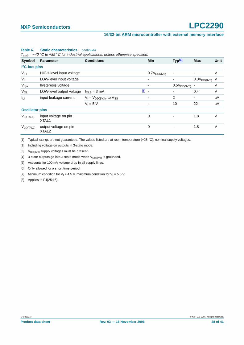
[1] Typical ratings are not guaranteed. The values listed are at room temperature (+25 °C), nominal supply voltages.
[2] Including voltage on outputs in 3-state mode.
[3] VDD(3V3) supply voltages must be present.
[4] 3-state outputs go into 3-state mode when VDD(3V3) is grounded.
[5] Accounts for 100 mV voltage drop in all supply lines.
[6] Only allowed for a short time period.
[7] Minimum condition for VI = 4.5 V, maximum condition for VI = 5.5 V.
[8] Applies to P1[25:16].
I2C-bus pins
VIH HIGH-level input voltage 0.7VDD(3V3) - - V
VIL LOW-level input voltage - - 0.3VDD(3V3) V
Vhys hysteresis voltage - 0.5VDD(3V3) - V
VOL LOW-level output voltage IOLS = 3 mA [5] - - 0.4 V
ILI input leakage current VI = VDD(3V3); to VSS - 2 4 µA
VI = 5 V - 10 22 µA
Oscillator pins
Vi(XTAL1) input voltage on pinXTAL1
0 - 1.8 V
Vo(XTAL2) output voltage on pinXTAL2
0 - 1.8 V
Table 6. Static characteristics …continuedTamb = −40 °C to +85 °C for industrial applications, unless otherwise specified.
Symbol Parameter Conditions Min Typ[1] Max Unit
LPC2290_3 © NXP B.V. 2006. All rights reserved.
Product data sheet Rev. 03 — 16 November 2006 28 of 41
NXP Semiconductors LPC229016/32-bit ARM microcontroller with external memory interface
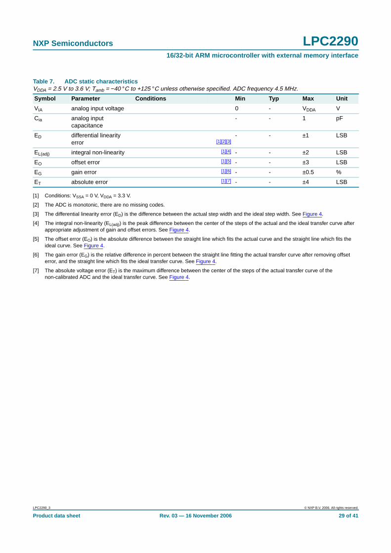
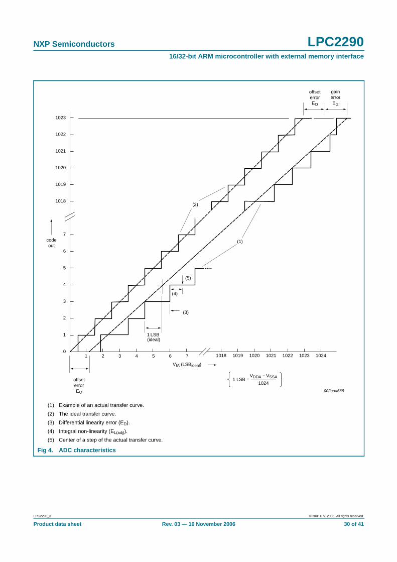
[1] Conditions: VSSA = 0 V, VDDA = 3.3 V.
[2] The ADC is monotonic, there are no missing codes.
[3] The differential linearity error (ED) is the difference between the actual step width and the ideal step width. See Figure 4.
[4] The integral non-linearity (EL(adj)) is the peak difference between the center of the steps of the actual and the ideal transfer curve afterappropriate adjustment of gain and offset errors. See Figure 4.
[5] The offset error (EO) is the absolute difference between the straight line which fits the actual curve and the straight line which fits theideal curve. See Figure 4.
[6] The gain error (EG) is the relative difference in percent between the straight line fitting the actual transfer curve after removing offseterror, and the straight line which fits the ideal transfer curve. See Figure 4.
[7] The absolute voltage error (ET) is the maximum difference between the center of the steps of the actual transfer curve of thenon-calibrated ADC and the ideal transfer curve. See Figure 4.
Table 7. ADC static characteristicsVDDA = 2.5 V to 3.6 V; Tamb = −40 °C to +125 °C unless otherwise specified. ADC frequency 4.5 MHz.
Symbol Parameter Conditions Min Typ Max Unit
VIA analog input voltage 0 - VDDA V
Cia analog inputcapacitance
- - 1 pF
ED differential linearityerror [1][2][3]
- - ±1 LSB
EL(adj) integral non-linearity [1][4] - - ±2 LSB
EO offset error [1][5] - - ±3 LSB
EG gain error [1][6] - - ±0.5 %
ET absolute error [1][7] - - ±4 LSB
LPC2290_3 © NXP B.V. 2006. All rights reserved.
Product data sheet Rev. 03 — 16 November 2006 29 of 41
NXP Semiconductors LPC229016/32-bit ARM microcontroller with external memory interface
(1) Example of an actual transfer curve.
(2) The ideal transfer curve.
(3) Differential linearity error (ED).
(4) Integral non-linearity (EL(adj)).
(5) Center of a step of the actual transfer curve.
Fig 4. ADC characteristics
002aaa668
1023
1022
1021
1020
1019
(2)
(1)
10241018 1019 1020 1021 1022 102371 2 3 4 5 6
7
6
5
4
3
2
1
0
1018
(5)
(4)
(3)
1 LSB(ideal)
codeout
VDDA − VSSA
1024
offseterrorEO
gainerrorEG
offseterrorEO
VIA (LSBideal)
1 LSB =
LPC2290_3 © NXP B.V. 2006. All rights reserved.
Product data sheet Rev. 03 — 16 November 2006 30 of 41
NXP Semiconductors LPC229016/32-bit ARM microcontroller with external memory interface
9. Dynamic characteristics
[1] Parameters are valid over operating temperature range unless otherwise specified.
[2] Bus capacitance Cb in pF, from 10 pF to 400 pF.
Table 8. Dynamic characteristicsTamb = −40 °C to +125 °C; VDD(1V8), VDD(3V3) over specified ranges.[1]
Symbol Parameter Conditions Min Typ Max Unit
External clock
fosc oscillator frequency supplied by an externaloscillator (signal generator)
1 - 50 MHz
external clock frequencysupplied by an externalcrystal oscillator
1 - 30 MHz
external clock frequency ifon-chip PLL is used
10 - 25 MHz
external clock frequency ifon-chip bootloader is usedfor initial code download
10 - 25 MHz
Tcy(clk) clock cycle time 20 - 1000 ns
tCHCX clock HIGH time Tcy(clk) × 0.4 - - ns
tCLCX clock LOW time Tcy(clk) × 0.4 - - ns
tCLCH clock rise time - - 5 ns
tCHCL clock fall time - - 5 ns
Port pins (except P0.2 and P0.3)
tr rise time - 10 - ns
tf fall time - 10 - ns
I2C-bus pins (P0.2 and P0.3)
tf fall time VIH to VIL[2] 20 + 0.1 × Cb - - ns
LPC2290_3 © NXP B.V. 2006. All rights reserved.
Product data sheet Rev. 03 — 16 November 2006 31 of 41
NXP Semiconductors LPC229016/32-bit ARM microcontroller with external memory interface
Table 9. External memory interface dynamic characteristicsCL = 25 pF, Tamb = 40 °C
Symbol Parameter Conditions Min Typ Max Unit
Common to read and write cycles
tCHAV XCLK HIGH to address validtime
- - 10 ns
tCHCSL XCLK HIGH to CS LOW time - - 10 ns
tCHCSH XCLK HIGH to CS HIGHtime
- - 10 ns
tCHANV XCLK HIGH to addressinvalid time
- - 10 ns
Read cycle parameters
tCSLAV CS LOW to address validtime
[1] −5 - +10 ns
tOELAV OE LOW to address validtime
[1] −5 - +10 ns
tCSLOEL CS LOW to OE LOW time −5 - +5 ns
tam memory access time [2][3] (Tcy(CCLK) × (2 + WST1)) +(−20)
- - ns
tam(ibr) memory access time (initialburst-ROM)
[2][3] (Tcy(CCLK) × (2 + WST1)) +(−20)
- - ns
tam(sbr) memory access time(subsequent burst-ROM)
[2][4] Tcy(CCLK) + (−20) - - ns
th(D) data hold time [5] 0 - - ns
tCSHOEH CS HIGH to OE HIGH time −5 - +5 ns
tOEHANV OE HIGH to address invalidtime
−5 - +5 ns
tCHOEL XCLK HIGH to OE LOW time −5 - +5 ns
tCHOEH XCLK HIGH to OE HIGHtime
−5 - +5 ns
Write cycle parameters
tAVCSL address valid to CS LOWtime
[1] Tcy(CCLK) − 10 - - ns
tCSLDV CS LOW to data valid time −5 - +5 ns
tCSLWEL CS LOW to WE LOW time −5 - +5 ns
tCSLBLSL CS LOW to BLS LOW time −5 - +5 ns
tWELDV WE LOW to data valid time −5 - +5 ns
tCSLDV CS LOW to data valid time −5 - +5 ns
tWELWEH WE LOW to WE HIGH time [2] Tcy(CCLK) × (1 + WST2) − 5 - Tcy(CCLK) × (1 +WST2) + 5
ns
tBLSLBLSH BLS LOW to BLS HIGH time [2] Tcy(CCLK) × (1 + WST2) − 5 - Tcy(CCLK) ×(1 + WST2) + 5
ns
tWEHANV WE HIGH to address invalidtime
[2] Tcy(CCLK) − 5 - Tcy(CCLK) + 5 ns
tWEHDNV WE HIGH to data invalid time [2] (2 × Tcy(CCLK)) − 5 - (2 × Tcy(CCLK)) + 5 ns
tBLSHANV BLS HIGH to address invalidtime
[2] Tcy(CCLK) − 5 - Tcy(CCLK) + 5 ns
LPC2290_3 © NXP B.V. 2006. All rights reserved.
Product data sheet Rev. 03 — 16 November 2006 32 of 41
NXP Semiconductors LPC229016/32-bit ARM microcontroller with external memory interface
[1] Except on initial access, in which case the address is set up Tcy(CCLK) earlier.
[2] Tcy(CCLK) = 1⁄CCLK.
[3] Latest of address valid, CS LOW, OE LOW to data valid.
[4] Address valid to data valid.
[5] Earliest of CS HIGH, OE HIGH, address change to data invalid.
tBLSHDNV BLS HIGH to data invalidtime
[2] (2 × Tcy(CCLK)) − 5 - (2 × Tcy(CCLK)) + 5 ns
tCHDV XCLK HIGH to data validtime
- - 10 ns
tCHWEL XCLK HIGH to WE LOWtime
- - 10 ns
tCHBLSL XCLK HIGH to BLS LOWtime
- - 10 ns
tCHWEH XCLK HIGH to WE HIGHtime
- - 10 ns
tCHBLSH XCLK HIGH to BLS HIGHtime
- - 10 ns
tCHDNV XCLK HIGH to data invalidtime
- - 10 ns
Table 9. External memory interface dynamic characteristics …continuedCL = 25 pF, Tamb = 40 °C
Symbol Parameter Conditions Min Typ Max Unit
Table 10. Standard read access specifications
Access cycle Max frequency WST setting
WST ≥ 0; round up tointeger
Memory access time requirement
standard read
standard write
burst read - initial
burst read - subsequent 3× N/A
f MAX2 WST1+
tRAM 20 ns+--------------------------------≤ WST1
tRAM 20 ns+
tcy CCLK( )--------------------------------≥ 2–
tRAM tcy CCLK( ) 2 WST1+( )× 20 ns–≤
f MAX1 WST2+
tWRITE 5 ns+----------------------------------≤ WST2
tWRITE tCYC 5+–
tcy CCLK( )--------------------------------------------≥
tWRITE tcy CCLK( ) 1 WST2+( )× 5 ns–≤
f MAX2 WST1+
tINIT 20 ns+--------------------------------≤ WST1
tINIT 20 ns+
tcy CCLK( )--------------------------------≥ 2–
tINIT tcy CCLK( ) 2 WST1+( )× 20 ns–≤
f MAX1
tROM 20 ns+---------------------------------≤ tROM tcy CCLK( ) 20 ns–≤
LPC2290_3 © NXP B.V. 2006. All rights reserved.
Product data sheet Rev. 03 — 16 November 2006 33 of 41
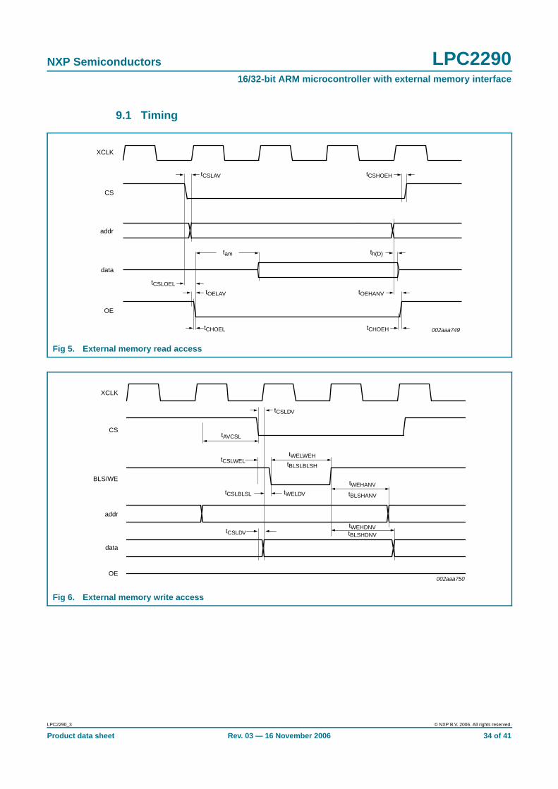
NXP Semiconductors LPC229016/32-bit ARM microcontroller with external memory interface
9.1 Timing
Fig 5. External memory read access
XCLK
CS
addr
data
OE
tCSLAV
tOELAV
tCSLOEL
tam th(D)
tCSHOEH
tOEHANV
tCHOEHtCHOEL 002aaa749
Fig 6. External memory write access
XCLK
CS
addr
data
BLS/WE
OE
tCSLWEL
tCSLBLSL tWELDV
tCSLDV
tWELWEH
tBLSLBLSH
tWEHANV
tBLSHANV
tWEHDNVtBLSHDNV
002aaa750
tCSLDV
tAVCSL
LPC2290_3 © NXP B.V. 2006. All rights reserved.
Product data sheet Rev. 03 — 16 November 2006 34 of 41
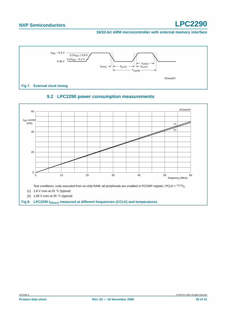
NXP Semiconductors LPC229016/32-bit ARM microcontroller with external memory interface
9.2 LPC2290 power consumption measurements
Fig 7. External clock timing
tCHCL tCLCX
tCHCX
Tcy(clk)
tCLCH
002aaa907
0.2VDD + 0.9 V
0.2VDD − 0.1 V
VDD − 0.5 V
0.45 V
Test conditions: code executed from on-chip RAM; all peripherals are enabled in PCONP register; PCLK = CCLK⁄4.
(1) 1.8 V core at 25 °C (typical)
(2) 1.65 V core at 25 °C (typical)
Fig 8. LPC2290 I DD(act) measured at different frequencies (CCLK) and temperatures
002aab452
frequency (MHz)0 60402010 5030
(1)
(2)
20
40
60
IDD current(mA)
0
LPC2290_3 © NXP B.V. 2006. All rights reserved.
Product data sheet Rev. 03 — 16 November 2006 35 of 41
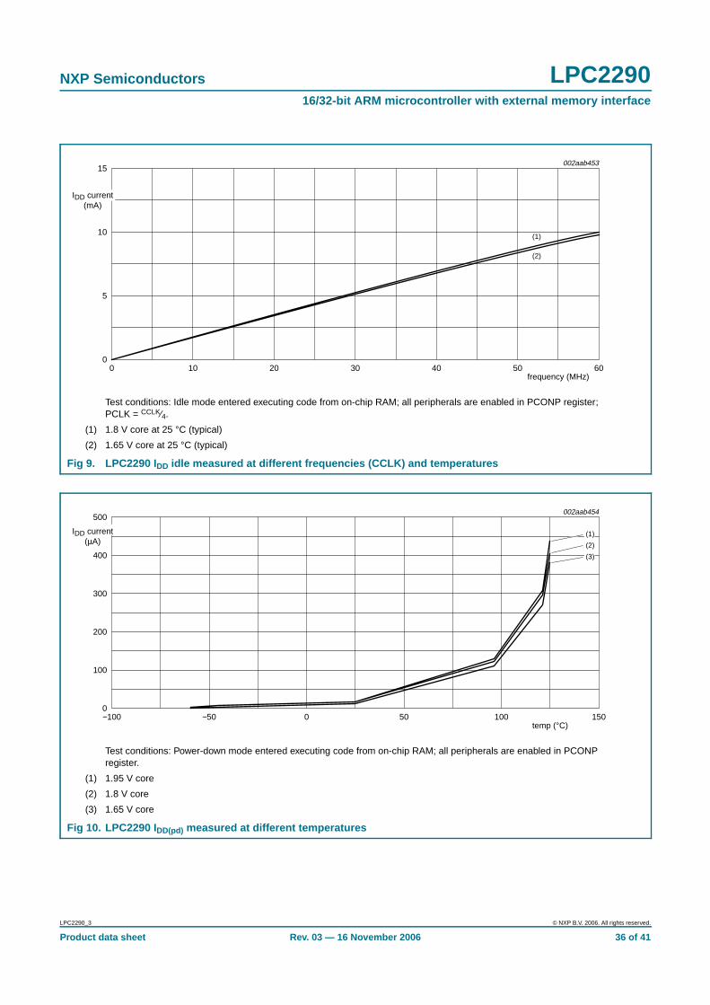
NXP Semiconductors LPC229016/32-bit ARM microcontroller with external memory interface
Test conditions: Idle mode entered executing code from on-chip RAM; all peripherals are enabled in PCONP register;PCLK = CCLK⁄4.
(1) 1.8 V core at 25 °C (typical)
(2) 1.65 V core at 25 °C (typical)
Fig 9. LPC2290 I DD idle measured at different frequencies (CCLK) and temperatures
frequency (MHz)0 60402010 5030
002aab453
5
10
15
IDD current(mA)
0
(1)
(2)
Test conditions: Power-down mode entered executing code from on-chip RAM; all peripherals are enabled in PCONPregister.
(1) 1.95 V core
(2) 1.8 V core
(3) 1.65 V core
Fig 10. LPC2290 I DD(pd) measured at different temperatures
002aab454
200
300
100
400
500
0
temp (°C)−100 1501000 50−50
IDD current(µA)
(1)
(2)
(3)
LPC2290_3 © NXP B.V. 2006. All rights reserved.
Product data sheet Rev. 03 — 16 November 2006 36 of 41
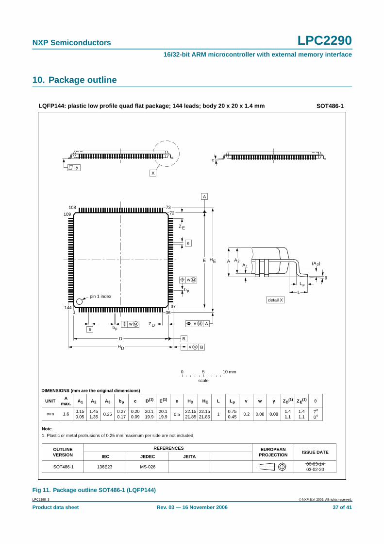
NXP Semiconductors LPC229016/32-bit ARM microcontroller with external memory interface
10. Package outline
Fig 11. Package outline SOT486-1 (LQFP144)
UNIT A1 A2 A3 bp c E(1) e HE L L p Zywv θ
REFERENCESOUTLINEVERSION
EUROPEANPROJECTION ISSUE DATE
IEC JEDEC JEITA
mm 0.150.05
1.451.35
0.250.270.17
0.200.09
20.119.9 0.5
22.1521.85
1.41.1
70
o
o0.080.2 0.081
DIMENSIONS (mm are the original dimensions)
Note
1. Plastic or metal protrusions of 0.25 mm maximum per side are not included.
0.750.45
SOT486-1 136E23 MS-02600-03-1403-02-20
D(1) (1)(1)
20.119.9
HD
22.1521.85
EZ
1.41.1
D
0 5 10 mm
scale
bpe
θ
EA1
A
Lp
detail X
L
(A )3
B
c
bp
EH A2
DH v M B
D
ZD
A
ZE
e
v M A
Xy
w M
w M
Amax.
1.6
LQFP144: plastic low profile quad flat package; 144 leads; body 20 x 20 x 1.4 mm SOT486-1
108
109
pin 1 index
7372
371
14436
LPC2290_3 © NXP B.V. 2006. All rights reserved.
Product data sheet Rev. 03 — 16 November 2006 37 of 41
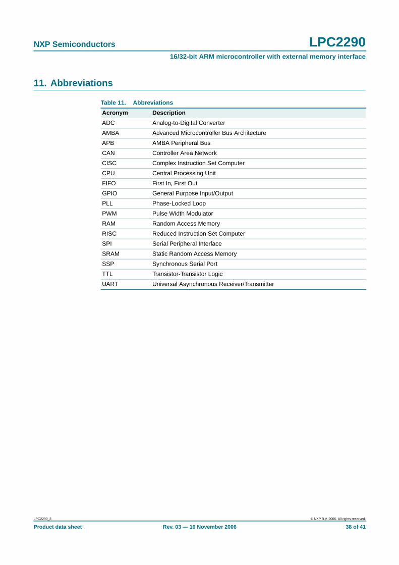
NXP Semiconductors LPC229016/32-bit ARM microcontroller with external memory interface
11. Abbreviations
Table 11. Abbreviations
Acronym Description
ADC Analog-to-Digital Converter
AMBA Advanced Microcontroller Bus Architecture
APB AMBA Peripheral Bus
CAN Controller Area Network
CISC Complex Instruction Set Computer
CPU Central Processing Unit
FIFO First In, First Out
GPIO General Purpose Input/Output
PLL Phase-Locked Loop
PWM Pulse Width Modulator
RAM Random Access Memory
RISC Reduced Instruction Set Computer
SPI Serial Peripheral Interface
SRAM Static Random Access Memory
SSP Synchronous Serial Port
TTL Transistor-Transistor Logic
UART Universal Asynchronous Receiver/Transmitter
LPC2290_3 © NXP B.V. 2006. All rights reserved.
Product data sheet Rev. 03 — 16 November 2006 38 of 41
NXP Semiconductors LPC229016/32-bit ARM microcontroller with external memory interface
12. Revision history
Table 12. Revision history
Document ID Release date Data sheet status Change notice Supersedes
LPC2290_3 20061116 Product data sheet - LPC2290-02
Modifications: • The format of this data sheet has been redesigned to comply with the new identityguidelines of NXP Semiconductors.
• Legal texts have been adapted to the new company name where appropriate.
• New features specific to the LPC2290/01 have been added throughout.
LPC2290-02 20041223 Product data - LPC2290-01
LPC2290-01 20040209 Preliminary data - -
LPC2290_3 © NXP B.V. 2006. All rights reserved.
Product data sheet Rev. 03 — 16 November 2006 39 of 41
NXP Semiconductors LPC229016/32-bit ARM microcontroller with external memory interface
13. Legal information
13.1 Data sheet status
[1] Please consult the most recently issued document before initiating or completing a design.
[2] The term ‘short data sheet’ is explained in section “Definitions”.
[3] The product status of device(s) described in this document may have changed since this document was published and may differ in case of multiple devices. The latest product statusinformation is available on the Internet at URL http://www.nxp.com.
13.2 Definitions
Draft — The document is a draft version only. The content is still underinternal review and subject to formal approval, which may result inmodifications or additions. NXP Semiconductors does not give anyrepresentations or warranties as to the accuracy or completeness ofinformation included herein and shall have no liability for the consequences ofuse of such information.
Short data sheet — A short data sheet is an extract from a full data sheetwith the same product type number(s) and title. A short data sheet is intendedfor quick reference only and should not be relied upon to contain detailed andfull information. For detailed and full information see the relevant full datasheet, which is available on request via the local NXP Semiconductors salesoffice. In case of any inconsistency or conflict with the short data sheet, thefull data sheet shall prevail.
13.3 Disclaimers
General — Information in this document is believed to be accurate andreliable. However, NXP Semiconductors does not give any representations orwarranties, expressed or implied, as to the accuracy or completeness of suchinformation and shall have no liability for the consequences of use of suchinformation.
Right to make changes — NXP Semiconductors reserves the right to makechanges to information published in this document, including withoutlimitation specifications and product descriptions, at any time and withoutnotice. This document supersedes and replaces all information supplied priorto the publication hereof.
Suitability for use — NXP Semiconductors products are not designed,authorized or warranted to be suitable for use in medical, military, aircraft,space or life support equipment, nor in applications where failure ormalfunction of a NXP Semiconductors product can reasonably be expected to
result in personal injury, death or severe property or environmental damage.NXP Semiconductors accepts no liability for inclusion and/or use of NXPSemiconductors products in such equipment or applications and thereforesuch inclusion and/or use is at the customer’s own risk.
Applications — Applications that are described herein for any of theseproducts are for illustrative purposes only. NXP Semiconductors makes norepresentation or warranty that such applications will be suitable for thespecified use without further testing or modification.
Limiting values — Stress above one or more limiting values (as defined inthe Absolute Maximum Ratings System of IEC 60134) may cause permanentdamage to the device. Limiting values are stress ratings only and operation ofthe device at these or any other conditions above those given in theCharacteristics sections of this document is not implied. Exposure to limitingvalues for extended periods may affect device reliability.
Terms and conditions of sale — NXP Semiconductors products are soldsubject to the general terms and conditions of commercial sale, as publishedat http://www.nxp.com/profile/terms, including those pertaining to warranty,intellectual property rights infringement and limitation of liability, unlessexplicitly otherwise agreed to in writing by NXP Semiconductors. In case ofany inconsistency or conflict between information in this document and suchterms and conditions, the latter will prevail.
No offer to sell or license — Nothing in this document may be interpretedor construed as an offer to sell products that is open for acceptance or thegrant, conveyance or implication of any license under any copyrights, patentsor other industrial or intellectual property rights.
13.4 TrademarksNotice: All referenced brands, product names, service names and trademarksare the property of their respective owners.
I2C-bus — logo is a trademark of NXP B.V.
14. Contact information
For additional information, please visit: http://www .nxp.com
For sales office addresses, send an email to: salesad [email protected]
Document status [1] [2] Product status [3] Definition
Objective [short] data sheet Development This document contains data from the objective specification for product development.
Preliminary [short] data sheet Qualification This document contains data from the preliminary specification.
Product [short] data sheet Production This document contains the product specification.
LPC2290_3 © NXP B.V. 2006. All rights reserved.
Product data sheet Rev. 03 — 16 November 2006 40 of 41
NXP Semiconductors LPC229016/32-bit ARM microcontroller with external memory interface
15. Contents
1 General description . . . . . . . . . . . . . . . . . . . . . . 12 Features . . . . . . . . . . . . . . . . . . . . . . . . . . . . . . . 12.1 Enhancements introduced with LPC2290/01
device . . . . . . . . . . . . . . . . . . . . . . . . . . . . . . . . 12.2 Key features common for LPC2290 and
LPC2290/01 . . . . . . . . . . . . . . . . . . . . . . . . . . . 13 Ordering information . . . . . . . . . . . . . . . . . . . . . 23.1 Ordering options . . . . . . . . . . . . . . . . . . . . . . . . 24 Block diagram . . . . . . . . . . . . . . . . . . . . . . . . . . 35 Pinning information . . . . . . . . . . . . . . . . . . . . . . 45.1 Pinning . . . . . . . . . . . . . . . . . . . . . . . . . . . . . . . 45.2 Pin description . . . . . . . . . . . . . . . . . . . . . . . . . 56 Functional description . . . . . . . . . . . . . . . . . . 146.1 Architectural overview. . . . . . . . . . . . . . . . . . . 146.2 On-chip SRAM . . . . . . . . . . . . . . . . . . . . . . . . 146.3 Memory map. . . . . . . . . . . . . . . . . . . . . . . . . . 146.4 Interrupt controller . . . . . . . . . . . . . . . . . . . . . 156.4.1 Interrupt sources. . . . . . . . . . . . . . . . . . . . . . . 166.5 Pin connect block . . . . . . . . . . . . . . . . . . . . . . 176.6 External memory controller. . . . . . . . . . . . . . . 176.7 General purpose parallel I/O and Fast I/O . . . 176.7.1 Features . . . . . . . . . . . . . . . . . . . . . . . . . . . . . 176.7.2 Fast I/O features available in LPC2290/01
only . . . . . . . . . . . . . . . . . . . . . . . . . . . . . . . . . 186.8 10-bit ADC . . . . . . . . . . . . . . . . . . . . . . . . . . . 186.8.1 Features . . . . . . . . . . . . . . . . . . . . . . . . . . . . . 186.8.2 ADC features available in LPC2290/01 only . . 186.9 CAN controllers and acceptance filter . . . . . . 186.9.1 Features . . . . . . . . . . . . . . . . . . . . . . . . . . . . . 186.10 UARTs . . . . . . . . . . . . . . . . . . . . . . . . . . . . . . 186.10.1 Features . . . . . . . . . . . . . . . . . . . . . . . . . . . . . 186.10.2 UART features available in LPC2290/01 only . 196.11 I2C-bus serial I/O controller . . . . . . . . . . . . . . 196.11.1 Features . . . . . . . . . . . . . . . . . . . . . . . . . . . . . 196.12 SPI serial I/O controller. . . . . . . . . . . . . . . . . . 196.12.1 Features . . . . . . . . . . . . . . . . . . . . . . . . . . . . . 206.13 SSP serial I/O controller (available in
LPC2290/01 only) . . . . . . . . . . . . . . . . . . . . . . 206.13.1 Features . . . . . . . . . . . . . . . . . . . . . . . . . . . . . 206.14 General purpose timers . . . . . . . . . . . . . . . . . 206.14.1 Features . . . . . . . . . . . . . . . . . . . . . . . . . . . . . 206.14.2 Timer features available in LPC2290/01 only . 216.15 Watchdog timer. . . . . . . . . . . . . . . . . . . . . . . . 216.15.1 Features . . . . . . . . . . . . . . . . . . . . . . . . . . . . . 216.16 Real-time clock . . . . . . . . . . . . . . . . . . . . . . . . 216.16.1 Features . . . . . . . . . . . . . . . . . . . . . . . . . . . . . 216.17 Pulse width modulator . . . . . . . . . . . . . . . . . . 22
6.17.1 Features . . . . . . . . . . . . . . . . . . . . . . . . . . . . . 226.18 System control . . . . . . . . . . . . . . . . . . . . . . . . 236.18.1 Crystal oscillator. . . . . . . . . . . . . . . . . . . . . . . 236.18.2 PLL. . . . . . . . . . . . . . . . . . . . . . . . . . . . . . . . . 236.18.3 Reset and wake-up timer . . . . . . . . . . . . . . . . 236.18.4 External interrupt inputs . . . . . . . . . . . . . . . . . 246.18.5 Memory mapping control . . . . . . . . . . . . . . . . 246.18.6 Power control . . . . . . . . . . . . . . . . . . . . . . . . . 246.18.7 APB bus . . . . . . . . . . . . . . . . . . . . . . . . . . . . . 246.19 Emulation and debugging. . . . . . . . . . . . . . . . 256.19.1 EmbeddedICE . . . . . . . . . . . . . . . . . . . . . . . . 256.19.2 Embedded trace. . . . . . . . . . . . . . . . . . . . . . . 256.19.3 RealMonitor . . . . . . . . . . . . . . . . . . . . . . . . . . 257 Limiting values . . . . . . . . . . . . . . . . . . . . . . . . 268 Static characteristics . . . . . . . . . . . . . . . . . . . 279 Dynamic characteristics . . . . . . . . . . . . . . . . . 319.1 Timing . . . . . . . . . . . . . . . . . . . . . . . . . . . . . . 349.2 LPC2290 power consumption measurements 3510 Package outline . . . . . . . . . . . . . . . . . . . . . . . . 3711 Abbreviations . . . . . . . . . . . . . . . . . . . . . . . . . 3812 Revision history . . . . . . . . . . . . . . . . . . . . . . . 3913 Legal information . . . . . . . . . . . . . . . . . . . . . . 4013.1 Data sheet status . . . . . . . . . . . . . . . . . . . . . . 4013.2 Definitions . . . . . . . . . . . . . . . . . . . . . . . . . . . 4013.3 Disclaimers. . . . . . . . . . . . . . . . . . . . . . . . . . . 4013.4 Trademarks . . . . . . . . . . . . . . . . . . . . . . . . . . 4014 Contact information . . . . . . . . . . . . . . . . . . . . 4015 Contents. . . . . . . . . . . . . . . . . . . . . . . . . . . . . . 41
© NXP B.V. 2006. All rights reserved.For more information, please visit: http://www.nxp.comFor sales office addresses, please send an email to: [email protected]
Date of release: 16 November 2006
Document identifier: LPC2290_3
Please be aware that important notices concerning this document and the product(s)described herein, have been included in section ‘Legal information’.
Related Documents