LEB and Vertex 2001 Trip report Gabriele Chiodini Fermilab, October 15, 2001 – Monday pixel meeting

LEB and Vertex 2001 Trip report Gabriele Chiodini Fermilab, October 15, 2001 – Monday pixel meeting.
Jan 02, 2016
Welcome message from author
This document is posted to help you gain knowledge. Please leave a comment to let me know what you think about it! Share it to your friends and learn new things together.
Transcript

LEB and Vertex 2001 Trip report
Gabriele ChiodiniFermilab, October 15, 2001 – Monday pixel meeting

G.Chiodini - Oct 15, 2001 - Fermilab 2
Attended conferences
7th Workshop on Electronics forLHC Experiments. Stockholm,Sweden, 10-14 Sep. 2001.
Plenary sessions:• Partially depleted SOI; • Trends: DSM, FPGA, and PCB.• LHC status; electronics for
Cal, Pix and AMS in space.• Hera-B commissioning.Parallel sessions:• Tracker FE –Trigger electronics• B+Rad effs –Cal electronics• Optoelec. -DAQ and DCS• Muons FE -GND+cooling+align.How to win a Nobel price!!!
10th International workshop onvertex detectors. Brunnen,Switzerland 23-28 Sep. 2001. Only plenary sessions:• Operating vertex• Planned vertex• Sensors• Detector readout• Triggering with vertex• Hybridization and
monolithic• Other applications

G.Chiodini - Oct 15, 2001 - Fermilab 3
LEB01: Partially depleted SOI (K. Bernstein - IBM)
• QM limitation to scaling law requires new concepts : PD SOI , DTMOS, FinFET, …
-------------------------------• Floating body effect in SOI.• PD SOI operation mode:
equilibrium, dynamic, steady.
• Delay: spatial + temporal.• Advantages:
– Less C SIMOX = 4.1, Si = 12).– Lower threshold.– No Latch-up.
• Applications: SRAM, powerPC, …
• Very few analog circuit in SOI.
Bulk MOSFET
PD SOI

G.Chiodini - Oct 15, 2001 - Fermilab 4
Trend in industry(1)• Scaling in DSM (K. Bernstein-IBM):
– Now tox= 0.1 um (0.25 um is 4 generation beyond ).– Scaling limitation due to QM (Roll-off from Morthy’s law if not innovation).– Problems: Process spread (yield), power and temperature distribution,
electromigration, hot carriers, SEU from surrounding material, oxide scaling (5 atoms, Igate is an issue), interconnect capacitive coupling, V drop.
– Innovation:• Device : DP SOI, FinFeT, Strained Si MOSFET. • Package: Chip Stack Module, 3D neural network.• System: Compiler and multiprocessor parallelism (it’s the future:no monster
chip).
• PC board (J.Bovier- Creative Electronic System)– Strong demand from new chip and technology: BGA and FBGA, fast
dynamic, multi PS, good cooling, low EMI.– New board require a high level designs (no change after).– Software testability (for example: JTAG chain).– BGA and FPGA package limits the re-workability. – Follow the design rules and stay in contact with your provider.– 18 month PC board delivering for CES.

G.Chiodini - Oct 15, 2001 - Fermilab 5
Trend in industry(2)• Progress in FPGA (P.Alfke - Xiling):
– PS: 1.5V (3.3V is dead, future 0.8V), good decoupling at LV is a problem.– Clock: 200MHz OK, > 500MHz need send clock+data (c is finite).– What we need:
• I/O levels.• serial Gbyte I/O.• embedded processor.• RAM or easy external RAM interface.
– Virtex-E (mature). Virtex-II (adolescent): multistandard I/O and efficient arithmetic. Virtex-II Pro (embryonic): MICROBLAZE 125 MHz on VirtexII.
• SEU in commercial FPGA (for space, S. Mattsson):– SETransient (for ex. glitch in the data or clock line) not seen in static mode.– Ions, protons,m and neutrons irradiation. – Antifuse an SRAM (often hang) based FPGA. – Xiling, Lucent, ATMEL, LATTICE, ACTEL, MEC.– Lower V more Upset, gold is bad, Xiling is on epilayer do not latch-up.– Xiling: regular FF and Triple red. FF, readback (bitstream repair).– Upset depend on frequency (non tested).– Ion: Xiling lower Eth than ACTEL but 100 time smaller cross section plateau.– Proton: Xiling cross section = 10E-14cm2, ACTEL 10 times more.– Neutrons: ? No beam direction? No packaging effect?

G.Chiodini - Oct 15, 2001 - Fermilab 6
LHC Status Reports(1)• LHC (T.Taylor):
– Commissioning: 1 January 2006. – LEP 90% dismounted.– Low beta 0.5m (0.25m you get SLHC, it’s feasible but BCO<25ns difficult).– Lattice dipole magnets from 3 companies: 3 working out of 4 (understood
why), more expensive than expected. Test all first 300-400 than decide. Production slope not bad but if problem show up they go out of schedule.
– Low beta quadrupoles from KEK and FNAL OK.– String test good. String2 test necessary for final installation.
• LHC Experiments: (J. Engelen)– Starting construction and learning how to do mass production.– FE more difficult than though (SLHC need to change all detectors).– CMS (4 reviews/year):
• Surface hall ready but cavern delayed by natural rock substitute by concrete• Yokes ready. Coil ready for 2004.• 223 m2 Si tracking: 200 detectors to exercise production + APV25 in DSM
good.• Pixel readout chip translated from DMILL to DSM.• Ecal: very noisy FE for APD. Muon: Drift chamber OK, RPC need oils to work
(big battle).• DAQ+Trigger: pilot project ready.

G.Chiodini - Oct 15, 2001 - Fermilab 7
LHC Status Reports(2)– ATLAS:
• Solenoid ready. 9m Prototype coil installed (goal 25m). 8 rings needed.• Tracker: pixel (DMILL to DSM FE issue) installed independently 1 year after
the tracker, SCT FE barrel OK, SCT FE end cup not OK.• Accordion Lar (no gaps) started electrodes production (more or less).• Tile Hcal very well. • Muons: stand-alone high precision big chambers (quality control for mass
production crucial).• DAQ+trigger go very well.
– LHCb:• Vertex: 300 um n-on-n single side, double metal layer microstrip.• Traker: silicon + straws.• Rich: HPD’s 1025 channels (500um x 500um), S/N=50, 25 MHz clock will be
reached in next version.• Ecal and Hcal OK.• Muon: RPC(no so good so far) + MWPC.
– ALICE:• Starting construction, TDR and R&D to do.• A lot of technologies involved but in good shape : pixel, SSD, SDD, RICH
(works at STAR), TPC, TOF ( multigap RPC is a novel concept dt=70ps), ECAL(CMS), L3 magnet.

G.Chiodini - Oct 15, 2001 - Fermilab 8
Electronics status reports– Hybrid pixel (M. Campell):
• ATLAS, CMS, BTeV, ALICE/LHCb. BTeV is very relevant and must be watched.• DSM: ALICE FE ready, LHCb next iteration BTeV FE almost ready.• DMILL: conversion in DSM: ATLAS and CMS.• 3D pixel=wire chamber with junction. No dead area, likely rad-hard. • Scaling: new current mode, dynamic range problems, LV problem.
– Cal (V. Radeka, “I encourage the people to be free to speak” ) :• Difficulty: large dynamic range (15-16 bit), uniformity and calibrations, fast.• CMS: 1fiber/crystal. No heat. Long tail killed by CMS (not for pile-up but
because radiation dependent) but ALICE can effort the tail. FNAL chip tested but noise larger and next iteration needed (inside 800 Mbit/s serializer). How much FE inside and outside? Problem of power.
• ATLAS: FE concentrated in the end of barrel (LHCb away few meter). In Tile-fiber the exponential tail is clipped (also if 5photoe/Mev!!!). Calibration problem with I constant and 0.1% accuracy due to parasitic L. Coherent noise is a problem, ground, shielding EMI to understand.
• FE good again in the next interaction!!!. LV regulator no progress (nobody wants work on CERN solution). Discrete component better than IC. Optical link still problems. Availability of technology is an issue (Vddd=3V). Spares and money.
• VLHC and SLHC: detectors are behind machine, rad effects, dynamic range issue.
• O.1 um good for digital but analog and mix is hard: tunneling gives large Igate.• Suggestion: Faraday cage between FE and detector in big system (Cu layer is
good).

G.Chiodini - Oct 15, 2001 - Fermilab 9
Hera-B electronic commissioning– In almost every subsystem there were surprises after assemblies:
• Rare and random chips and passive components failure.• Commercial optical link receiver: digital signals sensitive to particle flux.• LV broke soon, spikes in 240V, sensing failed.• Ground and shielding redesigned (also for crates).• Cross talk analog and digital lines.
– Lessons:• Hardware trigger must be tested also with no detector working.• SMT connector better than ST connector.• Quality of the board must be good.• Online masking of hot channels.• More expertise than one needed.• Software for commissioning need a lot of work.• GND, shielding and EMI critical.• Hardware needs to support debugging + on-line monitoring.• Use LVDS instead of open collector.• Regular ¾ month reviews from other experiments.

G.Chiodini - Oct 15, 2001 - Fermilab 10
Tracker FE (1)– ALICE (all DSM)
• SSD– HAL25 from ALICE28C 128 channels FE double side. JTAG programming
and controller, Reg with majority vote logic for SEU (new), OK but some yield problems.
– Ladder endcap electronics: controls 28 hybrids (6 FE chip/hybrid), power control, power protection (prevents latch-up, 1/m in PHOBE), readout, I/O buffering 25 m, JTAG. Solution 2 ASIC: analog buffer (now instable) + remaining functions (OK).
• Pixel– Very nice test stand: pci card in pc, vme interface, jtag, daq adapter
board. Used for wafer, bench, xray, Vpulse, beam. 65 kHz trigger rate. Labview + ROOT analysis. Calibration few minute per chip.
– Pilot chip to controls 5+5chips on ladder 1 and 2. 800 Gbit/s G-link compatible serializer and optical link receiver.
• SDD– large dynamic range FE and analog sampling (PASCAL chip OK). Huge
amount of data after digitations (AMBRA chip, good up to 60 Krad but memory die at 5 rad, now RAM in DSM). Two chips to avoid cross-talk.

G.Chiodini - Oct 15, 2001 - Fermilab 11
Tracker FE (2)– LHCb (all DSM)
• BEETLE1.1 chip for SVD, VETO?, RICH and more tested fine. 128 channel in pipeline, analog and binary readout not sparsified. 25 nsec peaking time (2 time worse than exp.). Submitted BEETLE-FE1.1-FE1.2-SR1.0 for improved peaking time and SEU hard regs and readback.
• ALICE1-LHCb for pixel and RICH. Qthmin<1000e@Qnoise<129e with sensor (no 3 bit adjust). LV=1.8V (1.6V designed). Reg redundancy. Sigma upset 60 Mev proton = 3e10-16cm2, Eth=5MeV mm2/mg. 12 Mrad OK. SPS 150GeV pion beam, good efficiency, working frequency = 10 MHz.
– ATLAS• SCT: Single side 12cm long sensors.
– ABCD3T chip in DMILL. Module tested in beam OK. Irradiation up to 3E14/cm2 need 500V and the TW=10 ns, timing change with irradiation. Good for p, gamma, pions. Starting production.
– SCT128A chip in DMILL. OK, 29%yield (3%FE+19%ADC+22%Dig+44%MUX).
• Pixel: MCM chip in DMILL. LVDS output link. Works OK up to 90 MHZ. 8 board irradiated at –30C up to 30 Mrad. After irradiation works up to 33 MHz (goal 40 MHz, simulation 80 MHz). Yield <50 %, actually 11%.

G.Chiodini - Oct 15, 2001 - Fermilab 12
Radiation and B effects on electronics– N and low gamma irradiation on commercial amp, switch, Vreg, DAC and ADC
(J.A. Agapito). – Low dose rate effect in test structure (for ABDC chip of ATLAS)
• Annealing is always beneficial and can not explain LDRE.• No LDRE observed in DMILL (max 0.5 krad/s up to 10 Mrad). Easy and more realistic
irradiation test. • Damage higher if you don’t bias (h trapped drift due to E). Someone says that the
opposite is true for CMOS. – Antifuse-FPGA for CMS DT in u-det tracker (1 rad/Y). ACTEL A54SX32 with
redundancy architecture and partition. SEU due to low energy h and n negligible. SEU < 2.9E-12cm2/chip (2.2SEU/y) for Ep=60 MeV. TID up to 20 krad OK, 40 krad still working.
– TID and SEU in FPGA in L1 muon for ATLAS (100rad/y). Xiling Virtex (2.5V) SRAM based:ASIC(1FF)=FPGA(30FF). SEU=4E-14cm2/bit and 1.6E-13 cm2/chip stack for 60 MeV p. Readback and reprogramming. 40 MHz clock, SEU not frequency dependent (I don’t believe it). In not-hardened flash PROM test SEU<1.3E-18cm2 !!!! 50 krad gamma after annealing is OK.
– CAEN: HV, LV modules tested with p (60MeV, 7krad=2e10p/cm2), gamma, n (60 MeV, 2E1011n/cm2), and under B (10 kGauss 5%-10% loss in worse case). Good for CMS u-det but ATLAS has 10 times more n.
– Atlas muon TDC LSI (Toshiba Gate array 0.3um CMOS) instead of FPGA. Slow PLL, SEU measurable but tolerable, no latch-up.

G.Chiodini - Oct 15, 2001 - Fermilab 13
Opto-electronics(1)– 75um precision CMS u-barrel alignment: n irradiation p(18MeV)
+Be up to 2.6E12 – 8E13 n/cm2 of COTS: LED (light decreases), LED driver, controller (SEU), lens, video sensor CMOS (synchronization and imaging lost at very end, OK with p but a lot of SEU) .
– GOL= Gbit/s data transmitter for LHC (P.Moreira: http://cern.ch/proj-gol).
• DSM, 32 bit/I, G-link and Gbit-Ethernet, 0.8-1.6Gbit/s. Redundancy in logic not in the serialiser, wire wired bits.
• Error free 4 day test but at 1.6MHz eye pattern not ideal (next version fix that).
• 10 Mrad 10 keV gamma no change. • SEU < 3.2E-13cm2 at 800 MHz for 60 MeV p. Ion test: Eth measured (5-
15MeVcm2/mg), increases with f, loss of lock is the dominant SEU. • SEU OK for serializer 10 times higher for PLL.• 100 samples to give to users. Few change for CMS and less SEU for
PLL.

G.Chiodini - Oct 15, 2001 - Fermilab 14
Opto-electronics(2)– LHCb RICH optical link trasmitter: GOL(800Mbit/s) + VCSEL+multimode
fibers. 1MHz not suppressed readout for L1. – Laser driver array for optical transmission at LHC (G. Cervelli).
DSM 3 channels for analogue and digital signals. Work very well, robust to Upset and total dose up to 20 Mrads. PDF of the production up to +/-3 sigma measured.
– QA manual for the CMS tracker optical links for environmental tests in pre-production and production (cal, B, rad, T, ageing, …). QA used in prototyping phase (after irr. discovered laser and photodiode dead and glass dark).
– Analogue opto-hybrids for CMS tracker extensively tested now starts pre-production. 17000 assembled pieces from 2002 to 2004.
– ATLAS SCT optical link. 30Mev,24GeV p and gamma: Truelight VCSEL <<1% failure after 10y. 10mA thr instead of 5 mA. Redundancy connections not increase noise. BER good. Package of 6hybrid+6flex. Ready for mass production.
– DMILL R/T optical link for ATLAS pixel: 80 MHz data Tr., 40 MHz clock and Bi-Phase Mark decoder. 25 GeV p irradiation. He didn’t show up.
– Optical link for ATLAS Tile-cal alternative to FPGA Chicago solution. Series of problems, now try with CERN device like GOL.

G.Chiodini - Oct 15, 2001 - Fermilab 15
Power distribution– Power supplies CMS-ECAL APD-HV. Tested CAEN
(SYS1527+HV4ch) and ISEG (HP-3858A HV8ch). Good ripple for both. Stability test CAEN is better (less variation, all channels behave the same).
– PS and distribution for ATLAS SCT. • 4088 module each one is own power cable. • 3 different cables: LM flex (Al)+LM special cable(Al, copper) +cable.
http:/merlot.ijs.si/~cindro/low_mass.html. • HV and LV together and twisted (cost? heat?too dense pack?). • Too many connectors and cables. Too late to optimize, next
prototype (Feb02) than pre-production (Apr02).• Maximum voltage drop highly above safety margin for ASIC’s. Rad
Hard regulator located in PP2 in R&D state.

G.Chiodini - Oct 15, 2001 - Fermilab 16
Operating vertex detectors (1)– CDF
• L00 pick-up noise from C fiber, removable by software but bad: S/N about 10.
• 5 DSSD layers (lessons):– Each layer is unique (5 sensor, 6/10 hybrids): reduce parts.– Difficult assembly (25% of all module need repair work): work in pipe-line and use
single side sensors.
• ISL: Every was very carefully tested before but in the final installation the cooling fluid doesn’t circulate. Glue blockage seen in Al elbow with new boroscope. October fixed with laser.
• Problem after installation:– 1.4% SVXII=1 wedge: damaged wires bonding on the port card– 2.8% SVXII=2 wedge: broken cable– 0.3%SVXII=½ ladder : has dead FE – Cooling ISL central part– Matching Inp/Out optical fiber impedance (introduce air or mylar, V up)– PS communication unreliable – Beam slope=0.6mrad (must be < 0.1mrad for vertexing); Beam center=3mm
(not < 1mm, lifetime compromised). Move all detector by 3 mm.
• Lessons:– Avoid custom made components – Long installation: delay from vendor too– Single component failures better affect efficiency and not acceptance.

G.Chiodini - Oct 15, 2001 - Fermilab 17
Operating vertex detectors (2)– D0
• 4Hdisk+6Barrel+12Fdisk DSSD. IP=30um up to eta<3.• Failure modes:
– 30% yield p-stop isolation defects in 90 degrees stereo angle.– Micro discharging effects: p-implants edge not aligned with electrodes.
• Lifetime limited by bypass capacitance.• Detector assembled and powered on:
– 15% chips not in the readout because they can not be downloaded (cables?, connectors?, chips?…). Should recover more 50% in October.
– Correlated noise. No sparsification up to now.
• Very good mechanical alignment (thanks Sidet)• Lessons:
– Use SSD– Much simpler design (with 6 sensor types were logistically very hard.
Big enterprise!!!)

G.Chiodini - Oct 15, 2001 - Fermilab 18
Operating vertex detectors (3)– Babar
• Rad hard up to 2 Mrad• ½ module not working out of 208. 1 dead module during operation • Power failure + magnet quenching.• Radiation:
– No radiation damage, hit efficiency 98%, dE/dx 2sigma sep. pion/K.– Radiation monitoring with pin diode. NIEL scaling works (dI~fluence).
Type inversion with e- (unexpected, no explanation). – Modules replacement 2004.
• Alignment crucial for sin(2beta):– Minimize residual now one plane each time but in the future inversion
of full matrix 6x(plane)E2 matrix.– Overlap hit very important for alignment, statistics not a problem.– Sin(2beta) measurements do not depend on the resolution function
parameterization.– New method necessary to extract lifetime better than PDG.

G.Chiodini - Oct 15, 2001 - Fermilab 19
Operating vertex detectors (4)– Belle
• DSSD (yield in each layer: 98.8%, 96.3%, 93.5%).• FE: VA1 (IDEAS, Norway) work well but loose gain 10 time faster than
expected (X ray beam losses was not noticed: orbit fixed + gold foil). Damaged modules replaced quickly and we could measure sin(2beta).
• 2002 upgraded vertex: more rad-hard DSSD, more rad tolerant chip VA2, new beam pipe (R=1.5 cm) for less background. (Luminosity increases fast).
• Difficult to predict any problem: radiation monitoring necessary (pin diode + radFET, do not use vertex).
– CleoIII• CVD diamond support. Reached < 2% Xo. • DSSD Hamamatzu:
– FE: BE chip Honeywell Rad-hard.– RC chip (CSEM): AC and Rbias on separate chip– Encapsulated wire bonds.
• 60% efficiency r-phi layer1 (z layers OK, layers 2-3 OK):– 3 broken Hybrid during installation.– 0% efficiency along rings getting worse with time (now also layer 2).
Radiation sickness already at 10-20 kRad. Vbias limited at 100 V. Encapsulation do not permit reworking.

G.Chiodini - Oct 15, 2001 - Fermilab 20
Operating vertex detectors (5)– Hera-B
• Large Roman pot system not interfering with Hera storage ring.• Two iteration needed to arrive to the final system.• Redundant pumping system: turbos + penning + Ti sublimation
(problems with Al cup out gassing at the begining).• Match beam impedance (shunt impedance Rs>100k for 52Mhz/f):
Al tube with holes, 4 Steel strip, 8 BeCu wires (all equivalent Rs reduced a factor of 100). (MAFIA32 3D software).
• No beam pick-up in the electronics (shielding works) but RF skin depth still not optimal (some RF resonances present).
• Binary Ice system with two cooling and pumping circuits for redundancy:
– Not recommended for T<-4C: viscosity increase, no benefits from binary system, safety hazard due to now explosive water-alcohol mixture.
– I will skip: H1, Zeus, STAR, PHOBOS and ATHENA. • First blast at RICH very scaring (PHOBOS: few % channels lost and
gain changed).

G.Chiodini - Oct 15, 2001 - Fermilab 21
Planned vertex (1) – CDF and D0 upgrade:
• SSD and high voltage detetcors • SVX4 in DSM• Few hybrid types.• Less material (for ex.: port card out of tracking region)• No double metal but kapton. No optical link but Cu transmission line (flex circuit).
– ATLAS SCT:• Sensors: Hamamatzu, CiS, Sintef• Termocycle for every hybrid and for subset of modules.• Pre-production is starting.
– ATLAS pixel:• Insertable layout. Less module more material in the forward region. One year
later others. • Al cooling pipe instead of C (broke at 8 Atm). Fluid C3F4.• Going in DSM (right now Qthrms=1000e- after 5 bit trimming) 50 Mrad radiation
test OK. • Module similar to BTeV. Thermal: C is strong and can break wire bonds (no so
far).• Chip in DSM: FE, MCC, VDC, DORIC. Engineering run in few weeks.• Sensor tiles: CiS gave good sensors (we don’t know the manufacture yield,
maybe 3 out of 15), Tesla gave no one (now maybe understood the problem). • 50 dummy module from two vendors. Assembly are going on but very slow
process.• Thinning not a problems (California vendors): plasma or lapping.

G.Chiodini - Oct 15, 2001 - Fermilab 22
Planned vertex (2) – CMS silicon tracker:
• A lot of tests: SSD Hamamatzu with p/n, AC coupled, polysilicon R , 300-500um, low resistivity, rho=1.5-3KOhmcm, metal overhang the p+ implant (500 to 600 V Vbreak).
• Crystal orientation <100> instead of usual <111)– Radiation up to 3E14 1 MeV eq n/cm2, Vdepl=280V.– Less interstrip capacitance.
• Layout details in the talk.• APV25 chip in DSM has pion SEU cross section few times larger than
us.
– CMS pixel:• SEU handled by frequent chip reset.• Sensor: 11GR single open p-ring hold 1000V (double break at 300 V)
– Single ring break at > 600 V after 6E1014p/cm2– Double and double crossed have 2 soft and hard breakdown after
irradiation (not present in diode, maybe premature breakdown for some pixels).
• Bump bonding in house capability (PSI)• P-spray is going to be developed at PSI.

G.Chiodini - Oct 15, 2001 - Fermilab 23
Planned vertex (3) – ALICE pixel:
• Qth<1000+/-200e- after 3 bit trimming, 32x256 pixels.• 6 wafer(86 chip each) tested at 300um and 750um thickness.• Yield: class I(30%), II(20 no injection more than 6000ch) ,III(20%), IV(30%bad).• Assemblies with AMS and VTT of p/n Canberra sensors (150-200um thick) and
chips on PC board acceptable (Thr and noise similar to bare chips). Test beam OK.
– LHCb tracker:• 9 stations, all different.• SSD p/n 6’’ wafer. –5C cold hydrogen box (Al foil + foam material).• Test beam with SPA (Kiev) detectors oxygenated and with multiguard rings.
They have too early breakdown.
– LHCb vertex locator (impact parameter trigger):• 1.3E13neq/cm2/y at 0.8 cm.• phi and r sensors. The r as 9 mm strip near the center.• Test beam: Double side Delphi, N+/n Hamamatzu and p/n micron. • SSD n+/n (from test beam), double metal and analog readout. • Impact parameter trigger with 150-250 pc. B would help a lot. New idea:
superL1.• L0 pile up VETO efficiency of 30-40% of single b-bbar events at optimal
luminosity.
G.Chiodini - Oct 15, 2001 - Fermilab 24
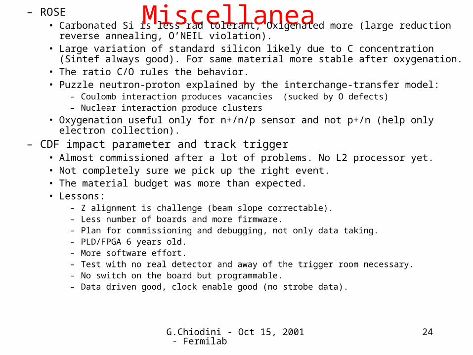
Miscellanea – ROSE• Carbonated Si is less rad tolerant, Oxigenated more (large reduction reverse
annealing, O’NEIL violation).• Large variation of standard silicon likely due to C concentration (Sintef always
good). For same material more stable after oxygenation.• The ratio C/O rules the behavior.• Puzzle neutron-proton explained by the interchange-transfer model:
– Coulomb interaction produces vacancies (sucked by O defects)– Nuclear interaction produce clusters
• Oxygenation useful only for n+/n/p sensor and not p+/n (help only electron collection).
– CDF impact parameter and track trigger• Almost commissioned after a lot of problems. No L2 processor yet.• Not completely sure we pick up the right event.• The material budget was more than expected.• Lessons:
– Z alignment is challenge (beam slope correctable).– Less number of boards and more firmware.– Plan for commissioning and debugging, not only data taking.– PLD/FPGA 6 years old.– More software effort.– Test with no real detector and away of the trigger room necessary.– No switch on the board but programmable.– Data driven good, clock enable good (no strobe data).

G.Chiodini - Oct 15, 2001 - Fermilab 25
Summary talk vertex2001 – C. Damerell
• Operating vertex very complex– Difficult to access and long sensor chain in one ladder. – Very sensitive to errors and beam losses.– QA precision necessary.– Group meeting, reviews, written document and worksheets necessary.– SSD preferred, but if DSD floating electronics recommended.– Wire bonds yield and thermal cycling necessary.
• Near future– Vertex with pixel (except LHCb), tracking with microstrip and gas
chambers.– Deep Submicron CMOS electronics. Concerns: LV and I protection.– Vertex triggering on-line: BTeV is going in the right direction.
• Linear collider– Hybrid pixel are almost ready but too much material (20 times more).– High speed column based CCD and Monolithic Active Pixel Sensor are
the preferred solution (not depleted device). Lot of progress but Rad-hardness must be tested (different from CMOS).
• A lot of not high energy applications.
Related Documents