1 1 CHAPTER 7 LATCH AND FLIP-FLOP 2 SEQUENTI AL CIRCUIT Called a circuit with memory. The output signals depend not only on the current inputs, but also the past sequence of input variables. Two types of sequential circuits: • Synchronous sequential circuits • Asynchro nous sequential circuit s

Welcome message from author
This document is posted to help you gain knowledge. Please leave a comment to let me know what you think about it! Share it to your friends and learn new things together.
Transcript

8/6/2019 Latch n Flip flop
http://slidepdf.com/reader/full/latch-n-flip-flop 1/26
1
1
CHAPTER 7
LATCH AND FLIP-FLOP
2
SEQUENTI AL CIRCUIT
Called a circuit with memory.
The output signals depend not only on the currentinputs, but also the past sequence of input variables.
Two types of sequential circuits:• Synchronous sequential circuits
• Asynchronous sequential circuits

8/6/2019 Latch n Flip flop
http://slidepdf.com/reader/full/latch-n-flip-flop 2/26
2
3
I) SYNCHRONOUS SEQUENTIAL CIRCUIT
• the output changes state only at a specified point on a triggeringinput called the clock (CLK), which is designated as a control input,C
• That is, the changes in the output occur in synchronization with theclock.
II) ASYNCHRONOUS SEQUENTIAL CIRCUIT
• depends on the inputs at only instance of time, whichthe input change.
• Refer to the events that do not have fixed timerelationship with each other, and generally do not occurat the same time
4
TERMINOLOGY
Multivibrator A class of digital circuits in which the output is connectedback to the input to produce either two stable states, onestable states, or no stable states, depending on theconfiguration.
Bistable Having two stable states. Flip-flop and latches are bistablemultivibrators.
Latch An asynchronous bistable multivibrator, used forstoring 1 bit.
Flip-Flop A synchronous bistable multivibrator, used forstoring 1 bit.
Asynchronous There is not fixed timing relationship.
Synchronous There is a fixed timing relationship, usuallythrough the use of a clock pulse
8/6/2019 Latch n Flip flop
http://slidepdf.com/reader/full/latch-n-flip-flop 3/26
3
5
Multivibrators
Bistable Monostable Astable
Latch Flip-Flop
S-RGated
S-RGated
D
Asynchronous synchronous
S-R
D
J-K
6
LAT CHES (SELAK )
The latch is a type of temporary storage device that has twostable states (bistable).
Basically is similar to FF because they are bistable devices that
can reside in either of two states using a feedback arrangement.
The main difference between latches and FF is in the method used for changing their state.
8/6/2019 Latch n Flip flop
http://slidepdf.com/reader/full/latch-n-flip-flop 4/26
4
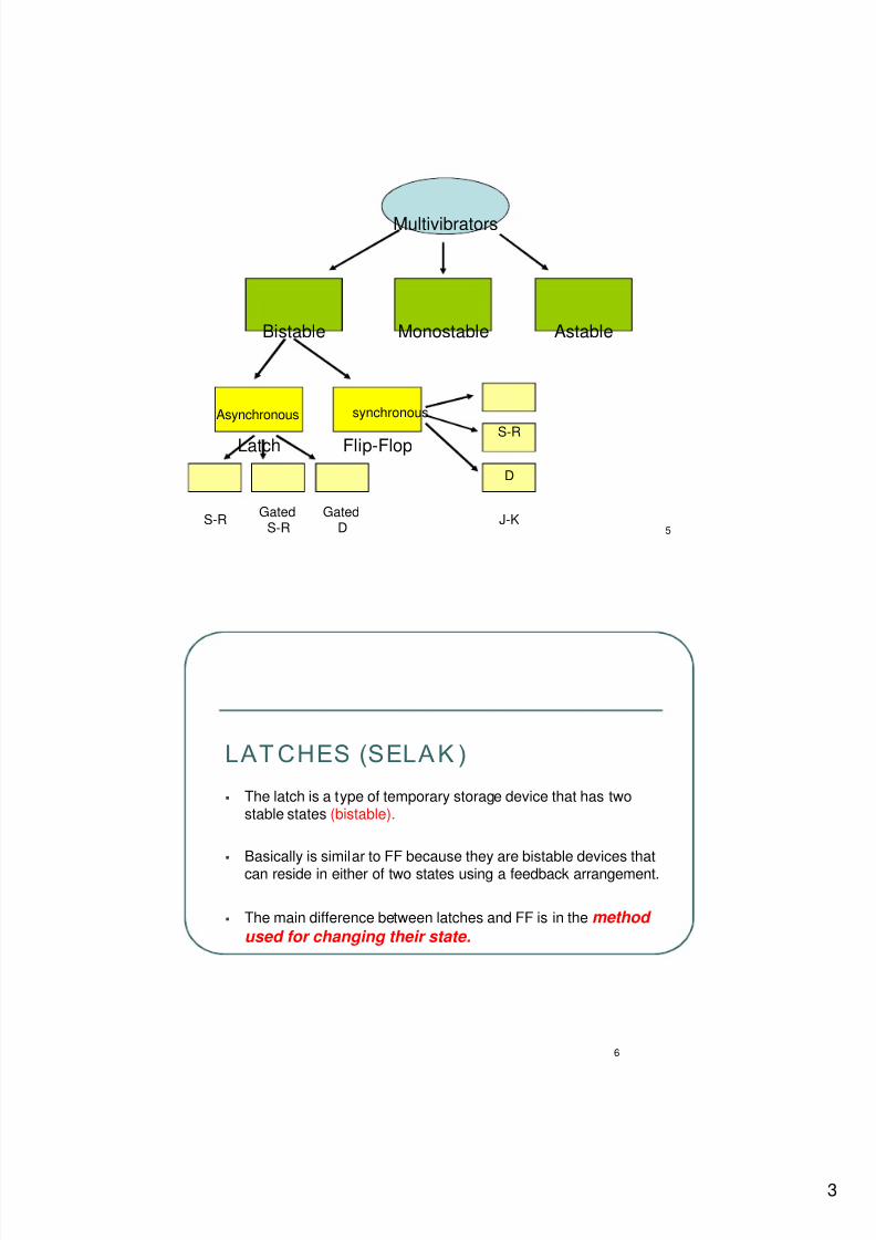
7
Latch
S-R GatedS-R
GatedD
Asynchronous
8
The S-R (SET-RESET) Latch (74LS279)
An active-HIGH input S-R (SET-RESET) latch is formed with two cross-coupled NOR gates.
An active-LOW input latch is formed with two cross-coupledNANDgates.
RS
8/6/2019 Latch n Flip flop
http://slidepdf.com/reader/full/latch-n-flip-flop 5/26
5
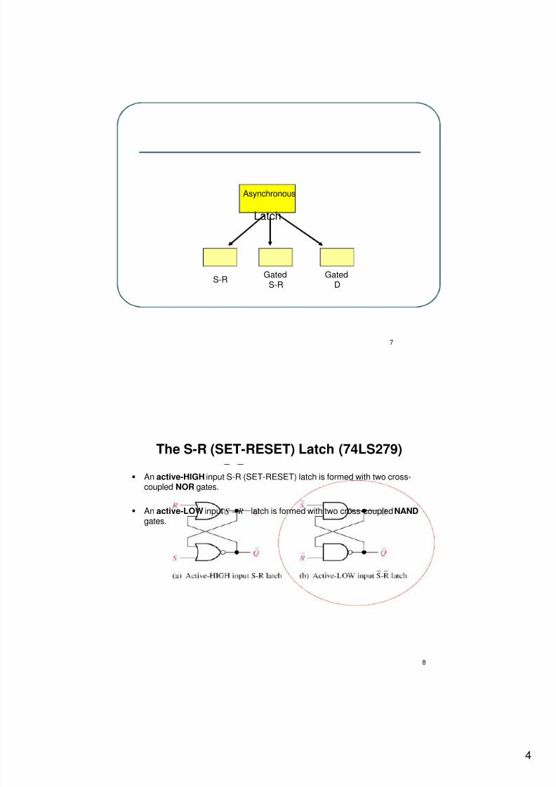
9
The S-R Latch
To explain the operation of the latch, we wil l use the OR gates withnegative/low inputs.
The latch is redrawn with the negative-OR equivalent symbols used forNAND gates.
Negative-OR equivalent ofthe NAND gate latch. RS
When Q is HIGH, is LOW, and when Q is LOW, is HIGH.Q Q
10
We can replace the and with the less confusing A and B respectively.
1) Let start by assuming that both inputs are 1 and Q = 1, therefore
S R
i) Let input A change to 0: ii ) Let input A change back to 1:
Summary:
For case i and ii , there is no change in Q, hence Q’ remains the same.
The S-R Latch

8/6/2019 Latch n Flip flop
http://slidepdf.com/reader/full/latch-n-flip-flop 6/26
6
11
2) Let input B change to 0:
Q changes to 0, hence Q’ change to 1
The circuit is now in a stable state.
Summary:
If Q=1, Q’=0, A=1 changing B from 1 to 0 RESETs Q to 0, Q’to 1
The S-R Latch
12
3) Let input A changes to 0:
Q will change to 1 and Q’ will change to 0
The circuit now in stable state.
Summary:
IF Q=0, Q’=1, B=1; A change from 1 to 0 SET Q to 1 and Q’ to 0.
The S-R Latch

8/6/2019 Latch n Flip flop
http://slidepdf.com/reader/full/latch-n-flip-flop 7/26
7
13
4) Previously we had A=0, B=1, Q=1 and Q’=0, let change B to 0.
Clearly, it is and INVALID Condition. Because Q=Q’
Summary:
The case of A=B=0 is to be avoided.
The S-R Latch
14
All this can summarized in the following truth-table:
A latch can reside in either of i ts twostates, SET or RESET
SET means that the Q output is HIGH.
RESET means that the Q output isLOW.
The S-R Latch
Logic symbols for both the active-HIGH input and the active-LOW input latchesare shown in figure below:

8/6/2019 Latch n Flip flop
http://slidepdf.com/reader/full/latch-n-flip-flop 8/26
8
15
The S-R Lat c h -- EXAMPLE
If the and waveforms in figure (a) below are applied tothe inputs of the active-LOW input latch, determine thewaveform that will be observed on the Q output. Assume Q isinitially LOW.
S R
RS
16
S-R Latch Application
If the switch bounce,means it is betweenposition 1 & 2,output will high. Aslong as switch DCfrom point 2, outputwill be high
If the switch bounce,means it is betweenposition 1 & 2,output will maintainbecause S-R willboth high, means NC
8/6/2019 Latch n Flip flop
http://slidepdf.com/reader/full/latch-n-flip-flop 9/26
9
17
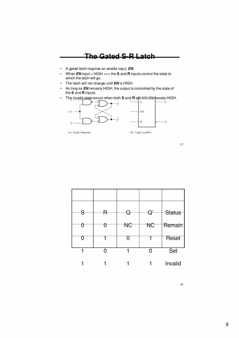
The Gated S-R Latch• A gated latch requires an enable input, EN .
• When EN input = HIGH ==> the S and R inputs control the state towhich the latch will go.
• The latch will not change until EN is HIGH.
• As long as EN remains HIGH, the output is controlled by the state ofthe S and R inputs.
• The invalid state occurs when both S and R are simultaneously HIGH.
18
S R Q Q’ Status
0 0 NC NC Remain
0 1 0 1 Reset
1 0 1 0 Set
1 1 1 1 Invalid

8/6/2019 Latch n Flip flop
http://slidepdf.com/reader/full/latch-n-flip-flop 10/26
10
19
Example (Gated S-R Latch)
20
The Gated D Latch

8/6/2019 Latch n Flip flop
http://slidepdf.com/reader/full/latch-n-flip-flop 11/26
11
21
22
Example (Gated D Latch)

8/6/2019 Latch n Flip flop
http://slidepdf.com/reader/full/latch-n-flip-flop 12/26
12
23
Flip-Flop
synchronous
S-R
D
J-K
24
Clock Pulse, Edge-Triggering
• The transition from state 0 to state 1 is called leading / positive / risingedge of the pulse.
• The transition from state 1 to state 0 is called trailing / negative / fallingedge of the pulse.
• The triggering of flip-flops can occur either at positive edge or negative edge.
• The time during which the clock is at logic 1 is called enable and the time
during which the clock is at logic 0 is called disable.• Unlike enable in latch, CLK just activate on the trigger time only not all on the
enable time.
Enable
Leading (positive)edge Diable
Trailing (negative)edge
0
1
Clock Pulse
8/6/2019 Latch n Flip flop
http://slidepdf.com/reader/full/latch-n-flip-flop 13/26
13
25
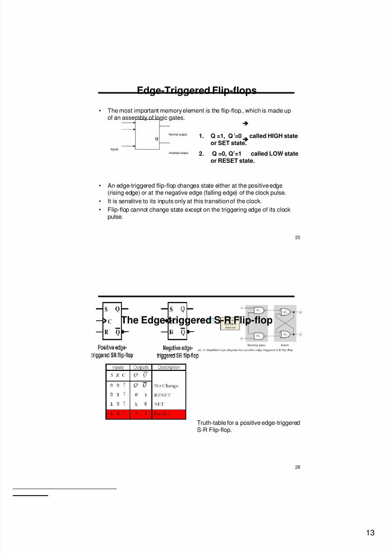
Edge-Triggered Flip-flops
• The most important memory element is the flip-flop., which is made upof an assembly of logic gates.
• An edge-triggered flip-flop changes state either at the positive edge
(rising edge) or at the negative edge (falling edge) of the clock pulse.• It is sensitive to its inputs only at this transition of the clock.
• Flip-flop cannot change state except on the triggering edge of its clockpulse.
.
.
.
.
Q
Normal output
Inverted output
Inputs
1. Q =1, Q ’=0called HIGH stateor SET state.
2. Q =0, Q’=1 called LOW stateor RESET state.
26
The Edge-triggered S-R Flip-flop
Truth-table for a positive edge-triggeredS-R Flip-flop.
8/6/2019 Latch n Flip flop
http://slidepdf.com/reader/full/latch-n-flip-flop 14/26
14
27
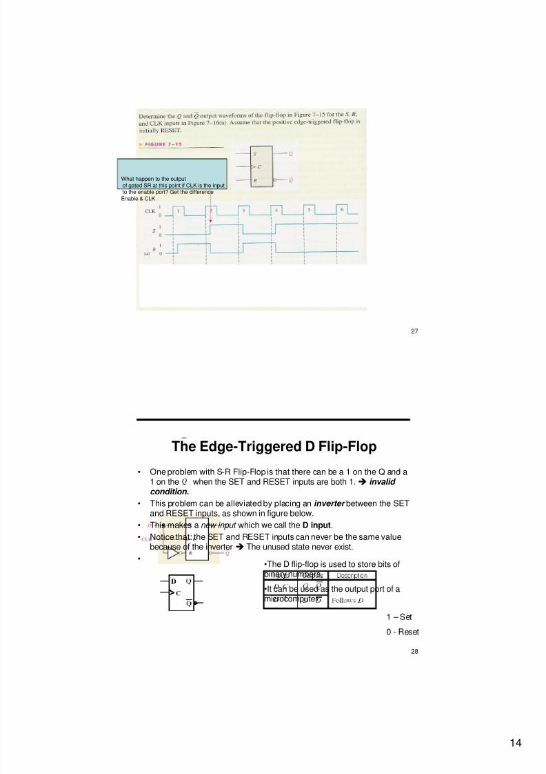
What happen to the output
of gated SR at this point if CLK is the inputto the enable port? Get the difference
Enable & CLK
28
The Edge-Triggered D Flip-Flop
• One problem with S-R Flip-Flop is that there can be a 1 on the Q and a1 on the when the SET and RESET inputs are both 1. invalid condition.
• This problem can be alleviated by placing an inverter between the SETand RESET inputs, as shown in figure below.
• This makes a new input which we call the D input.
• Notice that: the SET and RESET inputs can never be the same valuebecause of the inverter The unused state never exist.
•
Q
•The D flip-flop is used to store bits ofbinary numbers.
•It can be used as the output port of amicrocomputer.
1 – Set
0 - Reset

8/6/2019 Latch n Flip flop
http://slidepdf.com/reader/full/latch-n-flip-flop 15/26
15
29
Example:
Given the waveforms in figure (a) below for the D input and theclock, determine the Q output waveform if the flip-flop starts outRESET.
30
The Edge-Triggered J-K Flip-Flop
• The J-K flip-flop is versatile and is widely used type of flip-flop.
• The S-R edge-triggered flip-flop can be modified to become J-K edge-triggered flip-flop. The circuit is shown below.
• As can be seen the only changes in the JK flip-flop from the SR flip-flopare the additional feedback lines from the outputs to the oppositesteering gates.

8/6/2019 Latch n Flip flop
http://slidepdf.com/reader/full/latch-n-flip-flop 16/26
16
31
The Edge-Triggered J-K Flip-Flop
• The difference between the SR flip-flop and JK flip-flop is:
JK flip-flop has no invalid state as does the SR flip flop.
Summarized Truth-table Logic Symbols
32
Example
The waveforms in figure (a) below are applied to the J, K andclock inputs as indicated. Determine the Q output, assumingthat the flip-flop is initially RESET.

8/6/2019 Latch n Flip flop
http://slidepdf.com/reader/full/latch-n-flip-flop 17/26
17
33
Asynchronous Inputs
• Operate independently of the synchronous inputs and clock input
• Can be used to set the flip-flop to the 1 state or clear the flip-flop to 0state at any time, regardless of the conditions at the other inputs.
Designations for Asynchronous Inputs
• There are PRE, CLR, S D and R D .• But, the most common used designations are PRE and CLR .
• For the active-LOW status, we will use overbar to indicate them.
PRESET CLEAR Flip-flop response
1 1 Clocked operation.0 1 Q =1 (regardless of clock)
1 0 Q = 0 (regardless of clock)
0 0 Not used. (will give ambiguous response)
34
Asynchronous Preset and Clear Inputs
• Most integrated circuit flip-flop also have asynchronous inputs.
• These are inputs that affect the state of the flip-flop independent of the clock .
• An active level on the preset input will set the flip-flop.
• An active level on the clear input will reset the flip-flop.
• These preset and clear inputs must both be kept HIGH for
synchronous operation
Logic symbol for a JK flip-flop with
active LOW preset and clear inputs
.
Logic diagram for a basic JK flip-flop
with active LOW preset and clearinputs.

8/6/2019 Latch n Flip flop
http://slidepdf.com/reader/full/latch-n-flip-flop 18/26
18
35
Example:
For a positive edge-triggered JK flip-flop with preset and clearinputs in figure below, determine the Q output for the inputsshown in the timing diagram in part (a) if Q is initially LOW.
Flip-flop 7476
36
Flip-flop 7474
8/6/2019 Latch n Flip flop
http://slidepdf.com/reader/full/latch-n-flip-flop 19/26
19
37
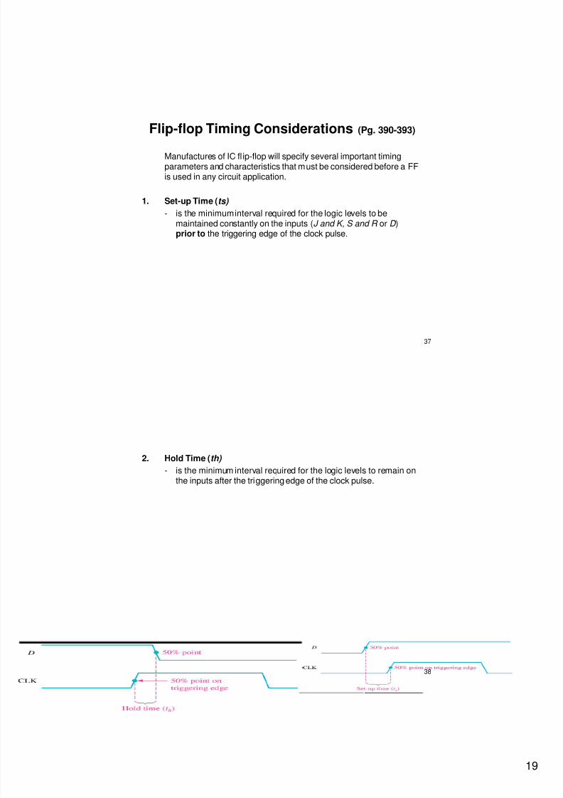
Flip-flop Timing Considerations (Pg. 390-393)
Manufactures of IC fl ip-flop will specify several important timingparameters and characteristics that must be considered before a FFis used in any circuit application.
1. Set-up Time (ts)
- is the minimum interval required for the logic levels to bemaintained constantly on the inputs (J and K, S and R or D )prior to the triggering edge of the clock pulse.
38
2. Hold Time (th)
- is the minimum interval required for the logic levels to remain onthe inputs after the triggering edge of the clock pulse.

8/6/2019 Latch n Flip flop
http://slidepdf.com/reader/full/latch-n-flip-flop 20/26
20
39
3. Propagation Delays
- is the interval of time required after an input signal has beenapplied for the resulting output change to occur.
- 4 categories of propagation delay are important in the operation ofa FF.
Measured from the triggering edge ofthe clock pulse to the LOW-to-HIGHtransition of output.
Measured from the triggeringedge of the clock pulse to theHIGH-to-LOW transition ofoutput.
40
Measured from the leadingedge of the preset input to theLOW-to-HIGH transition of theoutput.
Measured from the leadingedge of the clear input to theHIGH-to-LOW transition ofthe output.
8/6/2019 Latch n Flip flop
http://slidepdf.com/reader/full/latch-n-flip-flop 21/26
21
41
4. Maximum Clocking Frequency, fMax
- is the highest frequency that may be applied to the CLK input ofa FF.
- or is the highest rate at which FF can be reliably triggered.
- at clock frequencies above the maximum, the FF would beunable to respond quickly enough, and the operation would beimpaired.
- eg: For 7470 J-K flip-flop IC, its f MAX fall in the range 20 to 35MHz. So, he will specify the minimum f MAX as 20 MHz. Thismeans that; he cannot guarantee that the 7470 FF that you put inyour circuit will work above 20MHz. But, if you operate thembelow 20MHz, however; he guarantees that they will all work.
5. Pulse Widths (tw ) / Clock Pulse HIGH and LOW times
- the minimum time duration that the CLK signal must remain
LOW before it goes HIGH, sometimes called tw (L) , and theminimum time that CLK must kept HIGH before it returns LOW.Sometimes called tw (H).
42
6. Power Dissipation
- is the total power consumption of the device.
- Example:
If the FF operates on a +5V dc source and draws 5mA of current,the power dissipation is:
- Power dissipation is very important in most applications, inwhich the capacity of dc supply is concern.
- Example:
- It also tells you the output capacity required of the dc supply.
- Example:
If the FF operates on +5V dc, then the amount of current that thesupply must provide is:
mW mAV P CC 255
W mW mW PT 25.02502510
mAV
mW I 50
5
250

8/6/2019 Latch n Flip flop
http://slidepdf.com/reader/full/latch-n-flip-flop 22/26
22
43
Actual ICs
As practical examples of these timing parameters, let’s take a look at severalactual integrated-circuit FFs.
In particular, we will look at the following ICs:
7474 Dual edge-triggered D flip-flop (standard TTL)
74LS112 Dual edge-triggered J-K flip-flop (low power Schottky TTL)
74C74 Dual edge-triggered D flip-flop (metal-gate CMOS)
74HC112 Dual edge-triggered J-K flip-flop (high-speed CMOS)
44
Flip-Flop Applications
1. Contact Bounce Elimination
- When a mechanical switch is closed, the poles of the switch vibrateor bounce a number of times before finally making a solid contact.
- this bounces may produce voltage spikes, as shown in figure (a).
- Such voltage spikes are not desirable in a digital system.
- An SR latch can be used to eliminate the contact bounce as shown infigure (b).

8/6/2019 Latch n Flip flop
http://slidepdf.com/reader/full/latch-n-flip-flop 23/26
23
45
- The normal position of switch is 1.
- This input is LOW and latch is in RESET position.- When switch is thrown to position 2, goes HIGH due to
presence of pull up resistor to VCC and goes to LOW on thefirst contact.
- This SETs the latch.
- Any further voltage spikes on the input do not affect the latchand it remains SET.
- The Q output makes a clean transition from LOW to HIGH andvoltage spikes due to contact bounce are eliminated.
- A similar clean transition occurs when the switch is brought backto position 1.
R
R
S
S
46
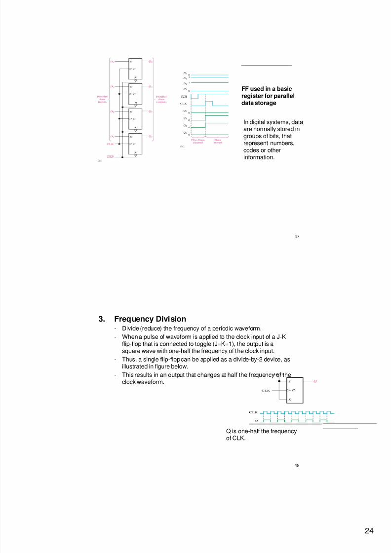
2. Parallel Data Storage in Registers
- Data storage is an important aspect of digital systems.
- Many data bits are taken on parallel lines and storedsimultaneously in a group of flip-flops.
- Figure (a) shows this parallel data input.
- The data inputs are connected to D0, D1 and D2 .
- The clock inputs of all the three flip-flops are tied together
and connected to common clock input.- This ensures that all the three flip-flops are triggered together.
- As shown in Figure (a), positive edge triggering is used inthis case.
- Therefore, the data is stored in flip-flops on the positiveedge of the clock.
- All the CLR terminals are also connected together, so that allthe three flip-flops are reset together.
- Groups of FF used to store data are known as registers incomputer terminology.
8/6/2019 Latch n Flip flop
http://slidepdf.com/reader/full/latch-n-flip-flop 24/26
24
47
FF used in a basic
register for paralleldata storage
In digital systems, dataare normally stored ingroups of bits, thatrepresent numbers,codes or otherinformation.
48
3. Frequency Division- Divide (reduce) the frequency of a periodic waveform.
- When a pulse of waveform is applied to the clock input of a J-Kflip-flop that is connected to toggle (J=K=1), the output is asquare wave with one-half the frequency of the clock input.
- Thus, a single flip-flop can be applied as a divide-by-2 device, asillustrated in figure below.
- This results in an output that changes at half the frequency of theclock waveform.
Q is one-half the frequencyof CLK.
8/6/2019 Latch n Flip flop
http://slidepdf.com/reader/full/latch-n-flip-flop 25/26
25
49
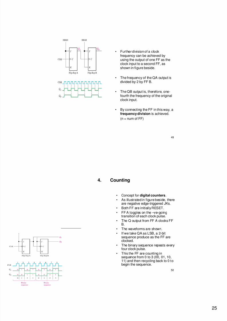
• Further division of a clock
frequency can be achieved byusing the output of one FF as theclock input to a second FF, asshown in figure beside.
• The frequency of the QA output isdivided by 2 by FF B.
• The QB output is, therefore, one-fourth the frequency of the originalclock input.
• By connecting the FF in this way, a
frequency division is achieved.
(n = num of FF)
50
4. Counting
• Concept for digital counters.
• As illustrated in figure beside, thereare negative edge-triggered JKs.
• Both FF are initially RESET.
• FF A toggles on the –ve-goingtransition of each clock pulse.
• The Q output from FF A clocks FF
B.• The waveforms are shown.
• If we take QA as LSB, a 2-bitsequence produce as the FF areclocked.
• The binary sequence repeats everyfour clock pulse.
• This the FF are counting insequence from 0 to 3 (00, 01, 10,11) and then recycling back to 0 tobegin the sequence.

8/6/2019 Latch n Flip flop
http://slidepdf.com/reader/full/latch-n-flip-flop 26/26
51
THE END
Related Documents