Laser Structuring of Organic Optoelectronic Devices To obtain the academic degree of Doctor Engineer (Dr.-Ing.) From the Department of Electrical Engineering and Information Technology Karlsruhe Institute of Technology (KIT) approved Dissertation from M.Sc. Joshua Alejandro Fragoso García Born in Mexico City, Mexico First Referee: Priv.-Doz. Dr.-Ing. Alexander Colsmann Second Referee: Prof. Dr. Bernhard Holzapfel Date of the oral exam: 14.02.2018

Welcome message from author
This document is posted to help you gain knowledge. Please leave a comment to let me know what you think about it! Share it to your friends and learn new things together.
Transcript

Laser Structuring ofOrganic Optoelectronic Devices
To obtain the academic degree of
Doctor Engineer (Dr.-Ing.)
From the Department of
Electrical Engineering and Information Technology
Karlsruhe Institute of Technology (KIT)
approved
Dissertation
from
M.Sc. Joshua Alejandro Fragoso García
Born in Mexico City, Mexico
First Referee: Priv.-Doz. Dr.-Ing. Alexander ColsmannSecond Referee: Prof. Dr. Bernhard HolzapfelDate of the oral exam: 14.02.2018


Laser Structuring ofOrganic Optoelectronic Devices
Zur Erlangung des akademischen Grades
DOKTOR-INGENIEURS
Von der Fakultät für Elektrotechnik und Informationstechni
des Karlsruher Institut für Technologie (KIT)
genehmigte Dissertation
von
M.Sc. Joshua Alejandro Fragoso García
geb. in Mexiko Stadt, Mexiko
Hauptreferent: Priv.-Doz. Dr.-Ing. Alexander ColsmannKorreferent: Prof. Dr. Bernhard HolzapfelTag der mündlichen Prüfung: 14.02.2018
k
s


Eidesstattliche Erklärung
Die vorliegende Arbeit wurde in der Zeit vom 01. Oktober 2013 bis zum 14. Februar 2018 amLichttechnischen Institut (LTI) des Karlsruher Instituts für Technologie (KIT) durchgeführtunter der Leitung von Herrn Priv.-Doz. Dr. Alexander Colsmann, LTI, KIT.
Ich versichere hiermit, dass ich die vorliegende Arbeit selbständig und unter Beachtung derRegeln zur Sicherung guter wissenschaftlicher Praxis im Karlsruher Institut für Technologie(KIT) in der aktuellen Fassung angefertigt habe. Ich habe keine anderen als die angegebenenQuellen und Hilfsmittel benutzt und wörtlich oder inhaltlich übernommene Stellen als solchekenntlich gemacht.
Karlsruhe, 15. 01. 2018
(Joshua A. Fragoso García)

Publication List
Articles in peer reviewed journalsJ. Fragoso, S.Höfle, M. Zhang, J. Dlugosch, T. Friedrich, S. Wager and A. Colsmann.OLED Luminaires: device arrays with 99.6% geometric fill factor structured by femtosecondlaser ablation, ACS Applied Materials & Interfaces. doi: 10.1021/acsami.7b12356
Articles in preparationJ. Fragoso, J. Dlugosch and A. Colsmann. Femtosecond multiwavelength ablation ITO onPET, Organic Electronics, in preparationGlaser & J. Fragoso, D. Bahro and A. Colsmann. A simple and fast experimental methodto find optimum design parameters for organic solar modules, Solar Energy Materials andSolar Cells, in preparationJ. Fragoso, T. Friedrich, D. Landerer, M. Koppitz and A. Colsmann. Invisible monolithicconnections in semitransparent all-solution organic solar modules, Energy Technology, inpreparation
Presentations at international conferencesJ. Fragoso, T. Friedrich, F. Nickel, D. Bahro, K. Glaser, J. Czolk, D. Landerer, M. Kop-pitz and A. Colsmann. Selective structuring of multilayers systems for organic solar cells,International Symposium on flexible Organic Electronics, Thessaloniki, Greece, 2016J. Fragoso, K. Glaser, J. Czolk, D. Landerer and A. Colsmann. Selective structuring ofpolymer multi-layers by femtosecond laser ablation, International laser & Coating Sympo-sium, Dresden, Germany, 2015J. Fragoso, D. Bahro, K. Glaser, F. Nickel and A. Colsmann. Laser structuring of tandemOPV modules, MatHero Summer School on Organic Photovoltaics, Freudenstadt, Germany,2015
iii

Publication List
Posters at international conferencesJ. Fragoso, F. Nickel and A. Colsmann. Femtosecond laser structuring of electrodes fororganic solar cells, MatHero Summer School on Organic Photovoltaics, Freudenstadt, Ger-many, 2015J. Fragoso, F. Nickel and A. Colsmann. Femtosecond laser structuring of electrodes for or-ganic solar cells, Large-area, Organic and Printed Electronics Convention (LOPEC), Munich,Germany, 2014J.Fragoso, F. Nickel and A. Colsmann. Femtosecond laser structuring of metal electrodesfor organic solar cells, 2nd International Next Generation Solar Energy (NGSE), Erlangen,Germany, 2013
iv

Supervised student works
M. Mertens. Laserinduzierte Herstellung von Nickeloxidschichten aus einem flüssigprozessiertenPräkursor, Master Thesis, Fakultät für Elektrotechnik und Informationstechnik, 2018 (inpreparation)F. Haberstroh. Near-Infrared Femtosecond Laser Ablation of Thin-Films for Organic Pho-tovoltaic Devices, Master Thesis, Karlsruhe School of Optics and Photonics, 2018J. Dlugosch. Laser processing of Nickel Oxide Precursor Films for Organic Photovoltaics,Master Thesis, Karlsruhe School of Optics and Photonics, 2017T. Friedrich. Selektive Laserstrukturierung von Polymerschichten für die organische Photo-voltaik, Masterarbeit, Fakultät für Elektrotechnik und Informationstechnik, 2016P. Böhler. Solution processed Nickel Oxide Hole Transport Layers for Organic Solar Cells,Bachelor Thesis, Department of Physics, Laboratory of Electron Microscopy, 2016T. Wünnemann Selektive Laserstrukturierung von organische Photovoltaik, Master Thesis
v


Summary
The future promise of organic electronics for a cheap production from solution has led tolarge investments in research and development. To take the research devices from lab scaleto the market, the structuring of them is necessary to connect the devices monolithically todecrease the resistance losses on the devices. Ultrashort pulsed lasers have been used for thispurpose in organic photovoltaic. They have also been used to structure the indium tin oxide(ITO) layer in different geometries for its application in other type of devices like organiclight emitting diodes (OLEDs).In this work the use of ultrashort pulsed lasers is investigated. Initially, the structuring ofITO on a mechanically flexible polyethylene substrate is studied. The ablation with differentwavelengths is explored. The ablation was then optimized to structure lines with low bulgesand selective ablation with negligible damage to the PET layer below. The structured lineswere optimized with different wavelengths in the visible regime.The ablation to monolithically connect OLEDs is then investigated. Devices with smallinactive areas that can be concealed by the illumination were manufactured. The power andcurrent efficiencies of these devices were improved by the decrease of the current and powerlosses on the devices. The structuring was optimized with two different wavelengths.In the next chapter, the structuring of OPV modules on ITO/glass substrates is explored.Different materials forming the active layer are investigated, demonstrating the feasibilityof using the ultrashort pulsed lasers to structure modules with different active layers. Thestructuring of tandem devices was also explored successfully fabricating working solar mod-ules. Finally, a method to experimentally optimized the solar cell width was investigated.In the last two chapter two different all-solution OPV architectures (semitransparent andopaque) are explored. The structuring was explored for different wavelengths in the visibleregime. Solar modules were then successfully manufactured. In both cases the structuringof the bottom electrode (PEDOT:PSS or silver) is essential as high bulges might lead toshortened devices.All the processes investigated in this work are an important step for the future fabricationof OPV and OLEDs.
vii


Contents
Publication List . . . . . . . . . . . . . . . . . . . . . . . . . . . . . . . . . . . . . . . . . iii
Supervised student works . . . . . . . . . . . . . . . . . . . . . . . . . . . . . . . . . . . v
Summary . . . . . . . . . . . . . . . . . . . . . . . . . . . . . . . . . . . . . . . . . . . . . vii
Contents . . . . . . . . . . . . . . . . . . . . . . . . . . . . . . . . . . . . . . . . . . . . . . ix
1 Introduction . . . . . . . . . . . . . . . . . . . . . . . . . . . . . . . . . . . . . . . . . 1
2 Fundamentals of organic semiconductors . . . . . . . . . . . . . . . . . . . . . . . 52.1 Organic semiconductors . . . . . . . . . . . . . . . . . . . . . . . . . . . . . . . . 52.2 Organic photovoltaics . . . . . . . . . . . . . . . . . . . . . . . . . . . . . . . . . 7
2.2.1 Working principle . . . . . . . . . . . . . . . . . . . . . . . . . . . . . . . 72.2.2 Interface materials in organic solar cells . . . . . . . . . . . . . . . . . . 102.2.3 Tandem solar cells . . . . . . . . . . . . . . . . . . . . . . . . . . . . . . . 122.2.4 Electrical characterization of organic solar cells . . . . . . . . . . . . . 132.2.5 Organic solar modules . . . . . . . . . . . . . . . . . . . . . . . . . . . . 15
2.3 Organic light emitting diodes . . . . . . . . . . . . . . . . . . . . . . . . . . . . . 162.3.1 Working principle . . . . . . . . . . . . . . . . . . . . . . . . . . . . . . . 162.3.2 Light emission and the role of the spin . . . . . . . . . . . . . . . . . . 162.3.3 OLED characterization . . . . . . . . . . . . . . . . . . . . . . . . . . . . 182.3.4 Upscaling of OLEDs . . . . . . . . . . . . . . . . . . . . . . . . . . . . . 19
3 Fabrication and characterization . . . . . . . . . . . . . . . . . . . . . . . . . . . . . 213.1 Sample preparation . . . . . . . . . . . . . . . . . . . . . . . . . . . . . . . . . . 21
3.1.1 Substrate preparation . . . . . . . . . . . . . . . . . . . . . . . . . . . . . 213.1.2 Layer application from solution . . . . . . . . . . . . . . . . . . . . . . . 213.1.3 Thermal evaporation layer application . . . . . . . . . . . . . . . . . . . 233.1.4 Cleanroom environment . . . . . . . . . . . . . . . . . . . . . . . . . . . 23
3.2 Characterization methods . . . . . . . . . . . . . . . . . . . . . . . . . . . . . . . 233.2.1 Topography characterization . . . . . . . . . . . . . . . . . . . . . . . . 233.2.2 Optoelectrical characterization . . . . . . . . . . . . . . . . . . . . . . . 25
3.3 Laser ablation setup . . . . . . . . . . . . . . . . . . . . . . . . . . . . . . . . . . 263.3.1 Ultrashort pulse amplifier (Libra) . . . . . . . . . . . . . . . . . . . . . 26
ix

CONTENTS
3.3.2 Ultrafast Optical parametric amplifier (OPerA Solo) . . . . . . . . . . 283.3.3 Workstation (µFAB, Newport) . . . . . . . . . . . . . . . . . . . . . . . 31
4 Laser principles . . . . . . . . . . . . . . . . . . . . . . . . . . . . . . . . . . . . . . . . 334.1 Working principle of a laser . . . . . . . . . . . . . . . . . . . . . . . . . . . . . 33
4.1.1 Light matter interaction . . . . . . . . . . . . . . . . . . . . . . . . . . . 344.1.2 Population inversion . . . . . . . . . . . . . . . . . . . . . . . . . . . . . 344.1.3 Feedback system . . . . . . . . . . . . . . . . . . . . . . . . . . . . . . . . 374.1.4 Types of lasers . . . . . . . . . . . . . . . . . . . . . . . . . . . . . . . . . 374.1.5 Q-Switching . . . . . . . . . . . . . . . . . . . . . . . . . . . . . . . . . . 374.1.6 Modelocking . . . . . . . . . . . . . . . . . . . . . . . . . . . . . . . . . . 384.1.7 Chirp Amplification . . . . . . . . . . . . . . . . . . . . . . . . . . . . . . 39
4.2 Wavelength tuning . . . . . . . . . . . . . . . . . . . . . . . . . . . . . . . . . . . 404.2.1 Optical parametric amplification . . . . . . . . . . . . . . . . . . . . . . 404.2.2 Sum-frequency generation . . . . . . . . . . . . . . . . . . . . . . . . . . 40
5 Laser processing . . . . . . . . . . . . . . . . . . . . . . . . . . . . . . . . . . . . . . . 435.1 Laser matter interaction . . . . . . . . . . . . . . . . . . . . . . . . . . . . . . . . 435.2 Nanosecond-laser ablation . . . . . . . . . . . . . . . . . . . . . . . . . . . . . . 45
5.2.1 Nanosecond ablation mechanisms . . . . . . . . . . . . . . . . . . . . . . 455.3 Ultrashort pulsed laser ablation . . . . . . . . . . . . . . . . . . . . . . . . . . . 47
5.3.1 Ablation mechanisms in dielectrics and metals . . . . . . . . . . . . . . 485.3.2 Theoretical threshold fluence determination . . . . . . . . . . . . . . . 49
5.4 Threshold fluence determination and pulse overlap . . . . . . . . . . . . . . . . 49
6 Femtosecond laser structuring of ITO on PET . . . . . . . . . . . . . . . . . . . . 516.1 Threshold fluence characterization . . . . . . . . . . . . . . . . . . . . . . . . . 516.2 Structuring process optimization . . . . . . . . . . . . . . . . . . . . . . . . . . 536.3 Discussion . . . . . . . . . . . . . . . . . . . . . . . . . . . . . . . . . . . . . . . . 58
7 OLED modules structured by femtosecond laser ablation . . . . . . . . . . . . . 617.1 Materials, device design and architecture . . . . . . . . . . . . . . . . . . . . . . 61
7.1.1 Materials . . . . . . . . . . . . . . . . . . . . . . . . . . . . . . . . . . . . 617.1.2 Architecture and sample design . . . . . . . . . . . . . . . . . . . . . . . 63
7.2 Threshold fluence characterization . . . . . . . . . . . . . . . . . . . . . . . . . 637.3 Structuring process optimization . . . . . . . . . . . . . . . . . . . . . . . . . . 65
7.3.1 ITO structuring (P1) . . . . . . . . . . . . . . . . . . . . . . . . . . . . . 657.3.2 ZnO/PEI/SuperYellow structuring (P2) . . . . . . . . . . . . . . . . . . 667.3.3 MoO3/silver (P3) structuring . . . . . . . . . . . . . . . . . . . . . . . . 67
7.4 Optoelectronic characterization . . . . . . . . . . . . . . . . . . . . . . . . . . . 677.5 Discussion . . . . . . . . . . . . . . . . . . . . . . . . . . . . . . . . . . . . . . . . 70
x

CONTENTS
8 Single-junction and tandem solar modules on top of ITO . . . . . . . . . . . . . 738.1 Materials . . . . . . . . . . . . . . . . . . . . . . . . . . . . . . . . . . . . . . . . . 748.2 Solar modules with PCDTBT:PC71BM . . . . . . . . . . . . . . . . . . . . . . 76
8.2.1 Architecture and solar module design . . . . . . . . . . . . . . . . . . . 768.2.2 Threshold fluences . . . . . . . . . . . . . . . . . . . . . . . . . . . . . . 778.2.3 Structuring process optimization . . . . . . . . . . . . . . . . . . . . . . 778.2.4 Electrical characterization . . . . . . . . . . . . . . . . . . . . . . . . . . 77
8.3 Solar modules with nanoparticulate P3HT:IC60BA . . . . . . . . . . . . . . . . 798.3.1 Architecture and solar module design . . . . . . . . . . . . . . . . . . . 798.3.2 Threshold fluences . . . . . . . . . . . . . . . . . . . . . . . . . . . . . . 798.3.3 Structuring process optimization . . . . . . . . . . . . . . . . . . . . . . 808.3.4 Electrical characterization . . . . . . . . . . . . . . . . . . . . . . . . . . 80
8.4 Tandem solar modules with PTB7:PC71BM . . . . . . . . . . . . . . . . . . . . 828.4.1 Architecture and solar module design . . . . . . . . . . . . . . . . . . . 838.4.2 Threshold fluences . . . . . . . . . . . . . . . . . . . . . . . . . . . . . . 838.4.3 Structuring process optimization . . . . . . . . . . . . . . . . . . . . . . 848.4.4 Electrical characterization . . . . . . . . . . . . . . . . . . . . . . . . . . 85
8.5 Rapid experimental optimization of the solar cell width . . . . . . . . . . . . . 868.6 Discussion . . . . . . . . . . . . . . . . . . . . . . . . . . . . . . . . . . . . . . . . 88
9 All-solution semi-transparent modules . . . . . . . . . . . . . . . . . . . . . . . . . 919.1 Materials and architecture . . . . . . . . . . . . . . . . . . . . . . . . . . . . . . 91
9.1.1 Materials . . . . . . . . . . . . . . . . . . . . . . . . . . . . . . . . . . . . 919.1.2 Architecture . . . . . . . . . . . . . . . . . . . . . . . . . . . . . . . . . . 93
9.2 Threshold fluences . . . . . . . . . . . . . . . . . . . . . . . . . . . . . . . . . . . 949.3 Structuring process optimization . . . . . . . . . . . . . . . . . . . . . . . . . . 95
9.3.1 PEDOT:PSS structuring (P1) . . . . . . . . . . . . . . . . . . . . . . . . 959.3.2 PBTZT-stat-BDTT-8:techPCBM (P2) structuring . . . . . . . . . . . 989.3.3 HYE (P3) structuring . . . . . . . . . . . . . . . . . . . . . . . . . . . . 100
9.4 Solar module characterization . . . . . . . . . . . . . . . . . . . . . . . . . . . . 1019.5 Discussion . . . . . . . . . . . . . . . . . . . . . . . . . . . . . . . . . . . . . . . . 102
10 All-solution opaque modules . . . . . . . . . . . . . . . . . . . . . . . . . . . . . . . 10510.1 Materials and device architecture . . . . . . . . . . . . . . . . . . . . . . . . . . 105
10.1.1 Materials . . . . . . . . . . . . . . . . . . . . . . . . . . . . . . . . . . . . 10510.1.2 Device architecture and design . . . . . . . . . . . . . . . . . . . . . . . 106
10.2 Threshold fluences . . . . . . . . . . . . . . . . . . . . . . . . . . . . . . . . . . . 10710.3 Structuring process optimization . . . . . . . . . . . . . . . . . . . . . . . . . . 108
10.3.1 Silver layer structuring (P1) . . . . . . . . . . . . . . . . . . . . . . . . . 10810.3.2 PBTZT-stat-BDTT-8:techPCBM layer structuring (P2) . . . . . . . . 11010.3.3 HYE (P3) structuring . . . . . . . . . . . . . . . . . . . . . . . . . . . . 111
xi

CONTENTS
10.4 Solar module characterization . . . . . . . . . . . . . . . . . . . . . . . . . . . . 11210.5 Discussion . . . . . . . . . . . . . . . . . . . . . . . . . . . . . . . . . . . . . . . . 113
11 Conclusions and outlook . . . . . . . . . . . . . . . . . . . . . . . . . . . . . . . . . . 115
A Single pulse threshold fluences . . . . . . . . . . . . . . . . . . . . . . . . . . . . . . 119
Bibliography . . . . . . . . . . . . . . . . . . . . . . . . . . . . . . . . . . . . . . . . . . . . 123
List of Figures . . . . . . . . . . . . . . . . . . . . . . . . . . . . . . . . . . . . . . . . . . 135
List of Tables . . . . . . . . . . . . . . . . . . . . . . . . . . . . . . . . . . . . . . . . . . . 139
Abbreviations . . . . . . . . . . . . . . . . . . . . . . . . . . . . . . . . . . . . . . . . . . . 141
Acknowledgements . . . . . . . . . . . . . . . . . . . . . . . . . . . . . . . . . . . . . . . 145
xii

1 Introduction
Organic Electronics is one of the most promising industrial sectors. It provides an alternativeto the mainstream silicon technologies and have several intrinsic advantages, such as thin-film devices, light weight, mechanical flexibility and the possibility of being produced atlow cost in roll-to-roll processes. Among the different technologies developed in the organicelectronics spectrum we can find organic light emitting devices (OLEDs) for both lighting anddisplay applications, organic photovoltaic devices (OPV), printed devices like temperatureand humidity sensors, batteries or memories. All these products have several applications fornumerous industries like packaging (sensors), automotive (lighting and energy production),building and architecture (lighting and energy production) among others. Together theseapplications represent a future market worth in excess of $ 70 billion by 2027, with a largepart of it being OLED displays.1
OLEDs are the most established technology within the context of organic electronics. Thefirst product to use an active-matrix OLED (AMOLED) was introduced by Kodak andSanyo in 2003 (Figure 1.1).2 Currently, AMOLEDs are used in displays in a whole varietyof products, like flat screen TVs, mobile phones, tablets etc. OLED lighting applicationsare already being tested. Audi’s swarm tail lights is one example of the use of OLEDs forlighting.3 The OLED backlighting technology used by AUDI resembles a screen, showing the
Figure 1.1: Camera by Kodak-Sanyo. First device with an OLED display introduced in 2003.2
1

1 Introduction
Figure 1.2: OPV integrated into sun glasses. The OPV device supplies energy for thermal and radiationintensity sensors.6
actions of the car´s driver. OLEDs have the advantage that they can also be processed fromsolution through roll-to-roll processes, avoiding costly high vacuum evaporation. However,this needs further exploration as the efficiency of the solution processed devices is not ashigh as the vacuum processed OLEDs.OPV are a promising energy technology that open new paths for novel applications. Itsintrinsic characteristics like light weight, semitransparency, color tunability, mechanical flex-ibility, roll-to-roll compatibility and low-light generation offer several advantages over themainstream silicon technology. Among all of these the most important one may be the low-light generation that enables indoor usage. The internet of things has led to an increasingamount of devices connected to the internet; not only mobile phones or tablets, also smart ledbulbs, cameras, sensors, etc. It is estimated that by 2020 there will be more than 50 billiondevices connected to the internet, more than 6 per person.4 All of these devices will increasepower consumption as they are supposed to be reachable at all times, therefore operatingfor long periods of time on standby. The electricity demand of these devices is expected togrow up to 1,140 TWh by 2025, accounting for 6% of the global electricity consumption.5
Just recently OPV have been integrated into sun glasses.6 (Figure 1.2) The glasses have anoutput of 400 µW, supplying energy, without batteries, for one temperature and irradiationsensors. The sensors work even under indoor lighting conditions, demonstrating a powerconversion efficiency of 6.2% at 500 lux.A not so mentioned advantage that OPV have over common crystalline silicon technologiesis the lower temperature coefficient. The temperature coefficient quantifies the tempera-ture sensitivity of the photovoltaic device.7 Common silicon solar modules have an averagetemperature coefficient between -0.37% and -0.52% C8. Therefore, when installed in hotweathers, where the solar resource is plenty, the performance is strongly hampered by thetemperature. OPV do not have this disadvantage as the temperature coefficient is slightlypositive 0.007% C.9 This improves the performance of the amount of kWh/kWp producedby OPV in hot temperature places where high irradiance is present.
2

Both OPV and OLED technologies help mitigate one of the largest problems humanity isfacing, Global Warming. As described above, the internet of things will require a total of1,140 TWh. These whole electricity consumption will generate more than 600 Mtons of CO2
to the atmosphere. This is a low estimate as a CO2 emission factor of 560 g kWh-1 is consid-ered. This is the emission factor reported for Germany over 2016.10 The capabilities of OPVwill expand the reach of renewable energies to produce energy inside our own houses. OLEDsare one highly energy efficient light source, hence the replacement of current luminaries withOLED luminaires will help to decrease the necessary electricity used in houses.OPV and OLED technologies require high precision structuring steps that allow the rightapplication of the technology. Ultrashort pulsed lasers are a unique tool that allows for highprecision and selective structuring of the thin film layers. Due to the cold ablation char-acteristics, the heat affected zone is minimized further increasing the precision. Currently,devices with a repetition rate of 200 kHz with a pulse energy of 1 mW are available in themarket.11 The high repetition rate allows the integration of the laser into a roll-to-roll devicewithout a significant decrease in the coating speed.In this work, a femtosecond laser source is used to selectively structure different organicelectronic devices (OLEDs and OPV).
3


2 Fundamentals of organicsemiconductors
This chapter covers the fundamental knowledge necessary to understand the function of OPVand OLEDs. Organic electronics exhibit semiconductor properties that enable the construc-tion of devices that are analogous to the ones used with inorganic semiconductors. Importantdifferences are present as the organic semiconductors do not have a valence band and conduc-tion band, instead they have a highest occupied orbital (HOMO) and lowest unoccupied orbital(LUMO). Due to the solution formation of some or all the layers, the upscaling of organicelectronics is different to the one of inorganic semiconductors. In section 2.1 the workingprinciples of organic semiconductors is explained. Section 2.2 covers the working principleof OPV, its characterization and the upscaling processes. Similarly, section 2.3 describes theworking principle of an OLED, its characterization and the upscaling processes.
2.1 Organic semiconductorsOrganic semiconductors are carbon based materials that exhibit semiconducting properties.Carbon is a chemical element with symbol C and atomic number 6. It has four valenceelectrons in its ground state. The electron distribution of carbon in its ground state isthe following: two electrons in the 1s orbital, two in the 2s orbital and the remaining twoin two of the three 2p orbitals. The ground state electronic configuration can be writtenas 1s22s22p1
x2p1y. The s orbitals are associated with a spherical charge distribution (Figure
2.1a) around the center of the atom, while the p orbitals have an 8 figure distribution (Figure2.1b). In the proximity of other carbon or hydrogen atoms that act as binding partners, theexerted external forces compensate the energy difference between the 2s and the 2p orbitals.
(a) (b) (c)
Figure 2.1: (a) s orbitals in the carbon atom. (b) p orbitals in the carbon atom. (c) Ethene molecule withthe sp orbitals forming σ bonds and the p orbitals forming π bonds.
5
2 Fundamentals of organic semiconductors
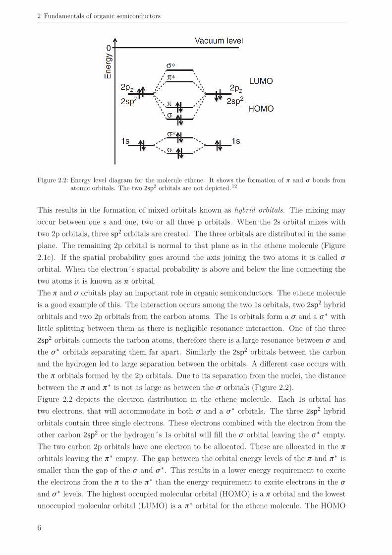
Figure 2.2: Energy level diagram for the molecule ethene. It shows the formation of π and σ bonds fromatomic orbitals. The two 2sp2 orbitals are not depicted.12
This results in the formation of mixed orbitals known as hybrid orbitals. The mixing mayoccur between one s and one, two or all three p orbitals. When the 2s orbital mixes withtwo 2p orbitals, three sp2 orbitals are created. The three orbitals are distributed in the sameplane. The remaining 2p orbital is normal to that plane as in the ethene molecule (Figure2.1c). If the spatial probability goes around the axis joining the two atoms it is called σ
orbital. When the electron´s spacial probability is above and below the line connecting thetwo atoms it is known as π orbital.The π and σ orbitals play an important role in organic semiconductors. The ethene moleculeis a good example of this. The interaction occurs among the two 1s orbitals, two 2sp2 hybridorbitals and two 2p orbitals from the carbon atoms. The 1s orbitals form a σ and a σ∗ withlittle splitting between them as there is negligible resonance interaction. One of the three2sp2 orbitals connects the carbon atoms, therefore there is a large resonance between σ andthe σ∗ orbitals separating them far apart. Similarly the 2sp2 orbitals between the carbonand the hydrogen led to large separation between the orbitals. A different case occurs withthe π orbitals formed by the 2p orbitals. Due to its separation from the nuclei, the distancebetween the π and π∗ is not as large as between the σ orbitals (Figure 2.2).Figure 2.2 depicts the electron distribution in the ethene molecule. Each 1s orbital hastwo electrons, that will accommodate in both σ and a σ∗ orbitals. The three 2sp2 hybridorbitals contain three single electrons. These electrons combined with the electron from theother carbon 2sp2 or the hydrogen´s 1s orbital will fill the σ orbital leaving the σ∗ empty.The two carbon 2p orbitals have one electron to be allocated. These are allocated in the πorbitals leaving the π∗ empty. The gap between the orbital energy levels of the π and π∗ issmaller than the gap of the σ and σ∗. This results in a lower energy requirement to excitethe electrons from the π to the π∗ than the energy requirement to excite electrons in the σand σ∗ levels. The highest occupied molecular orbital (HOMO) is a π orbital and the lowestunoccupied molecular orbital (LUMO) is a π∗ orbital for the ethene molecule. The HOMO
6

2.2 Organic photovoltaics
Figure 2.3: Hopping process in a disordered organic solid. r depicts the distance from the electrode. Thedashed line indicates the potential energy due to the electric field F.12
and the LUMO are called frontier orbitals. The energy difference between the HOMO andthe LUMO is analogous to the energy difference between the valence band and conductionband in the inorganic semiconductors and is responsible for the semiconductor properties oforganic materials.In order to use the semiconducting properties of organic materials, the charge carriers (holesand electrons) need to be extracted/injected. Due to the high and low energy levels of theσ and σ∗ it is difficult to achieve charge injection from the electrodes into these levels in themolecule. On the contrary, the π and π∗ have moderate energy levels that facilitate chargeinjection.Different to inorganic semiconductors, the orbitals do not form a regular uniform energyband, it is rather a collection of states where the charges move. Therefore, a so calledhopping process is the way the charge carriers propagate inside the organic semiconductor(Figure 2.3). This is one of the reasons why organic semiconductors have lower mobilities,in the range of 10-5 - 10-2 cm2 V-1 s-1, than inorganic semiconductors with mobilities in therange of 103 - 104 cm2 V-1 s-1.
2.2 Organic photovoltaics
2.2.1 Working principle
Organic solar cells have attracted large interest since they were discovered by Tang in 1986,who developed single heterojunction devices with an efficiency of about 1%.13 There aresubstantial differences between the common pn-junction solar cells made from crystallinesilicon and the ones made from organic semiconductors.14 15
7

2 Fundamentals of organic semiconductors
(a) (b)
Figure 2.4: (a) Bilayer heterojunction solar cell. 1) Light is absorbed close to the interface generating anexciton. The exciton is dissociated at the interface. The electron and hole are collected in thecathode and anode respectively. 2) The light is absorbed far from the interface generating anexciton that recombines afterward. (b) Bulk-heterojunction solar cell. The donor and acceptordomains are intermixed increasing the interface surface area. 1) The light is absorbed producingan exciton that is dissociated at the interface. The electron and hole are collected in the cathodeand anode respectively. 2) The light is absorbed producing an exciton that is dissociated. Thehole is trapped as it is located on an island with no contact to the anode. The hole will recombineafterwards.
• The absorption of a photon in an organic solar cell produces an excited state calledexciton (bound electron-hole pair). This exciton has a high binding energy of at least300 meV whereas excitons in inorganic semiconductors exhibit binding energies of aonly a few meV. To generate a current the excitons need to be dissociated. A secondmaterial, commonly called acceptor, is necessary for this dissociation. This materialwill provide an energy difference that is enough to separate the exciton.
• The diffusion length of the exciton is between 10 - 20 nm. If an exciton does not reachthe acceptor/donor interface, it would recombine and the energy would be lost as heat.
• Organic semiconductors have large extinction coefficients compared to crystalline sili-con. This leads to an efficient light harvesting in thin-films of 100 - 300 nm thickness.
• Organic solar cells are sandwiched between two electrodes with different work func-tions. A built-in potential appears, resulting in an electric field that helps the transportof charges. An organic solar cell is a drift device, whereas crystalline silicon solar cellsdepends mainly on diffusion processes.
An organic solar cell with an architecture similar to the one used by Tang is depicted inFigure 2.4a. The charges are usually absorbed on the donor material (Yellow). An exci-ton is created and it moves to the interfaces where it is dissociated (1). The hole is thencollected at the anode and the electrode at the cathode. If the exciton does not reach theinterface, it recombines (2). This type of architecture does not achieve high efficiencies. The
8

2.2 Organic photovoltaics
Figure 2.5: Energy levels of an organic solar cell. 1) Photons with higher energy than the bandgap areabsorbed. 2) Thermalization occurs and the exciton is formed. 3) Exciton diffusion to thematerial interface where it is dissociated. 4) Electron or holes are transferred to the acceptor ordonor respectively. The open circuit voltage is also indicated.14
layer thickness need to be ultrathin, approximately 20 nm to achieve appropriate excitondissociation due to the limited exciton diffusion length. Even with the large extinction co-efficients of organic solar cells, this thickness will not be sufficient to absorb a significantamount of light. A solution to increase the interface, while keeping the distance the excitonneeds to travel within the exciton diffusion length, is a bulk heterojunction (BHJ) (Figure2.4b). The materials are mixed together creating a morphology that allows to increase theinterface between the donor and acceptor. Similar to the bilayer-heterojunction, the lightis absorbed in the donor. The created exciton travels to the interface and the charges arecollected in the electrodes (1). However, some of the free charge carriers may not be able toreach their respective electrode as they are located in an island with no contact to the elec-trode. The charge carriers then recombine leading to higher losses on the device. Therefore,optimization of the BHJ morphology is necessary to decrease the recombination losses.Figure 2.5 shows the energy level diagrams of an organic solar cell.14 Photons with higherenergy than the bandgap are absorbed (1). The absorption may occur on both sides of theinterface. If the photon energy is higher than the bandgap, thermalization occurs and anexciton is formed (2). The exciton diffuses to the interface where it dissociates (3). Theelectrons are then transported to the cathode and the holes to the anode (4).One of the most important parameters for solar cells, the open-circuit voltage (Voc), isdepicted in Figure 2.5 for organic solar cells. The Voc is proportional to the energy gapbetween the HOMO level of the donor and the LUMO level of the acceptor. The V oc canbe calculated using the following empirical formula16:
Voc = 1
e(∣∣EHOMO,donor
∣∣− ∣∣ELUMO,acceptor∣∣)−0.3V (2.1)
9

2 Fundamentals of organic semiconductors
(a) (b)
Figure 2.6: Regular and inverted architectures with ITO and silver as top and bottom electrode. (a) Organicsolar cell with regular architecture: the position of the hole transport layer (HTL) on top of theITO defines it as the anode. (b) Organic solar cell with inverted architecture organic: the positionof the electron transport layer (ETL) on top of the ITO defines it as the cathode.
Where V oc is the open-circuit voltage, e is the elementary charge, EHOMO,donor is the HOMOlevel of the donor and ELUMO,acceptor is the LUMO level of the acceptor in eV. The 0.3 V isthe empirically calculated necessary energy to dissociate the electron.17
2.2.2 Interface materials in organic solar cells
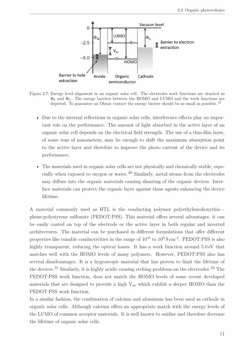
Interface materials have proved to help increasing the performance of organic solar cells.The functions of interface materials are:18 19
• Determines the device polarity. Regular and inverted architectures are used in organicsolar cells (Figure 2.6). Indium tin oxide (ITO) is commonly used as the bottomtransparent electrode while silver or aluminum are commonly used as the top elec-trode. Figure 2.6a shows the hole transport layer (HTL) on top of the ITO definingit as the anode for the regular architecture. On the contrary, figure 2.6b shows theelectron transport layer on top of the ITO defining it as the cathode for the invertedarchitecture.
• The interface materials should provide an ohmic electrode with the organic mate-rial. An ohmic electrode is capable to inject/extract more charges than can be trans-ported/produced in the device. This condition is defined as sustained space chargelimited current (SCL). Whether an electrode is able to sustain SCL conditions de-pends both on the extraction barrier and the charge carrier mobility of the organicsemiconductor. For ideal interfaces, the extraction barrier is defined by the energydifference between the work function of the electrodes and the HOMO of the donorand the LUMO of the acceptor (Figure 2.7). An estimate of an acceptable barrier is0.3 eV for a conjugated polymer with an average mobility of 10-4 cm2 V-1 s-1.12
10
2.2 Organic photovoltaics
Figure 2.7: Energy level alignment in an organic solar cell. The electrodes work functions are denoted asΦA and ΦC. The energy barriers between the HOMO and LUMO and the work functions aredepicted. To guarantee an Ohmic contact the energy barrier should be as small as possible.12
• Due to the internal reflections in organic solar cells, interference effects play an impor-tant role on the performance. The amount of light absorbed in the active layer of anorganic solar cell depends on the electrical field strength. The use of a thin-film layer,of some tens of nanometers, may be enough to shift the maximum absorption pointto the active layer and therefore to improve the photo current of the device and itsperformance.
• The materials used in organic solar cells are not physically and chemically stable, espe-cially when exposed to oxygen or water.20 Similarly, metal atoms from the electrodesmay diffuse into the organic materials causing shunting of the organic devices. Inter-face materials can protect the organic layer against these agents enhancing the devicelifetime.
A material commonly used as HTL is the conducting polymer polyethylenedioxythio -phene:polystyrene sulfonate (PEDOT:PSS). This material offers several advantages, it canbe easily coated on top of the electrode or the active layer in both regular and invertedarchitectures. The material can be purchased in different formulations that offer differentproperties like tunable conductivities in the range of 10-6 to 103 S cm-1. PEDOT:PSS is alsohighly transparent, reducing the optical losses. It has a work function around 5.0 eV thatmatches well with the HOMO levels of many polymers. However, PEDOT:PSS also hasseveral disadvantages. It is a hygroscopic material that has proven to limit the lifetime ofthe devices.21 Similarly, it is highly acidic causing etching problems on the electrodes.22 ThePEDOT:PSS work function, does not match the HOMO levels of some recent developedmaterials that are designed to provide a high Voc which exhibit a deeper HOMO than thePEDOT:PSS work function.In a similar fashion, the combination of calcium and aluminum has been used as cathode inorganic solar cells. Although calcium offers an appropriate match with the energy levels ofthe LUMO of common acceptor materials. It is well known to oxidize and therefore decreasethe lifetime of organic solar cells.
11

2 Fundamentals of organic semiconductors
Metal oxides offer an alternative to both PEDOT:PSS and the combination of calcium/alu-minum. Most metal oxides are robust and stable, eliminating the problem of the stabilitythat comes with the use of PEDOT:PSS or calcium. They can be processed from solutionusing different chemical precursors or can be evaporated in vacuum. There are several metaloxides with different work functions to choose in order to match the energy levels of thesemiconducting polymer materials.
2.2.3 Tandem solar cells
Similar to other photovoltaic devices, organic solar cells do not absorb light in the whole solarspectrum. This leads to absorption losses, due to photons that have less energy than thebandgap, and thermalization losses of high energy photons, caused by the electron relaxationafter the photon is absorbed. Therefore, an efficient way to absorb light along the wholesolar spectrum is necessary.23
A promising concept, that has been widely used in other photovoltaic technologies, is tohave two serially connected solar cells on top of each other. This is known as tandem ormultijunction solar cells (TSC). The absorption materials used in the TSC usually havecomplimentary absorption spectra, hence absorbing a larger part of the solar spectrum. Dueto the thin film nature of organic solar cells there is also a benefit from designing a TSCusing twice the same absorption material. This compensates for the low optical density ormoderate charge carrier transport properties of the material.24 The concept of homo-TSCand hetero-TSC is illustrated below (Figure 2.8).Due to the serial connection of TSC, they exhibit larger voltage and lower currents, resultingin the reduction of of resistive losses in the electrodes. The higher voltage also enables theuse of TSC to split water photochemically.26
Figure 2.8: Absorption spectrum coverage for homo and hetero tandem solar cells.25 The single junctionsolar cell efficiency is limited to the bottom left. The hetero-TSC complements the absorptionspectrum of the single solar cell (Right part), while the homo-TSC compensates for low opticaldensity (top part).
12

2.2 Organic photovoltaics
Tandem architectures have a theoretical maximum power conversion efficiency (PCE) limitof 15%.27 TSC with 13.2%28 have already been built, successfully demonstrating the appli-cation of this concept in organic solar cells.
2.2.4 Electrical characterization of organic solar cells
A solar cell can be approximated to a diode in the dark. A diode is a device that allows amuch larger current under forward bias (V >0) than under reverse bias (V <0), hence havinga rectifying behavior.29 For an ideal diode the dark current density Jdark is given by:
Jdark(V ) = Jo(eqV
kBT −1) (2.2)
Where Jo is a constant, K B is the Boltzmann constant and T is the temperature in Kelvin.When light shines on the device, a net photocurrent is produced that results from thesubtraction of the short circuit current J sc and the dark current, resulting in:
J = Jsc− Jo(eqV
kBT −1) (2.3)
When the contacts are isolated, the potential difference is maximized and the solar cellproduces the open circuit voltage (V oc). For the ideal diode this is given by:
Voc = kT
qln(
JscJo
+1) (2.4)
However, in real solar cells, the power is dissipated through the resistance of the contacts andthrough leakage currents. These effects can be electrically approximated to a series (Rs) andparallel (Rsh) resistance. The equivalent electrical circuit showing both Rs and Rsh, togetherwith the J sc and Jdark is shown in figure 2.9.If the parasitic resistances are considered the equation for the current of a solar cell becomes:
J = Jsc− Jo(eq(V +J ARs)
kBT −1)− V + J ARsRsh
(2.5)
Figure 2.9: Equivalent circuit of a solar cell. The series resistance of the electrodes is depicted as (Rs) andthe shunt resistance as (Rsh).
13

2 Fundamentals of organic semiconductors
Figure 2.10: Current density (black line) and power density (blue line) of a solar cell. The fill factor is theratio between the blue and the gray rectangles.
The power provided by a solar cell is P = JV . A solar cell has an optimum operating pointwhere it operates with the maximum efficiency. This point is know as the maximum powerpoint (MPP) at the voltage V mp and the current I mp. The ratio between the V mp the currentI mp and the V oc and current I sc is defined as fill factor (F F ). The FF is then given by:
F F = Vmp JmpVoc Jsc
(2.6)
Figure 2.10 depicts the fill factor as the ratio between the gray rectangle and the bluerectangle. J-V curves are used in this work instead of I-V curves to ease the comparison ofdifferent size devices.The power conversion efficiency (PCE) is the ratio of the extracted power over the incidentlight (P in):
PC E = Vmp JmpPin
(2.7)
The F F and the power conversion efficiency are then related by:
PC E = JscVocF F
Pin(2.8)
These four parameters J sc, V oc, F F and PC E are the key performance parameters. It isimportant to consider that the PCE is reported using standard test conditions (STC). TheSTC are defined as 1000 W m-2, air mass (AM) of 1.5 and 25°C. The air mass depends onthe path length that the light has to travel through the atmosphere to reach the position ofthe solar cells.
14

2.2 Organic photovoltaics
2.2.5 Organic solar modules
Most of the solar cells that are built on laboratory scale are in the square millimeter scale,making the electrical losses due to the resistance of the semi-transparent electrode irrelevant.When an organic solar cell is upscaled, the resistance losses increase as the path that thecharges need to travel, is longer. In addition the photocurrent grows with the area, increasingthe power losses P loss = V I 2. A common solution is to limit the size of the solar cells, thereforelimiting the current and the power losses. The solar cells are then serially connected in asolar module through a monolithic connection (Figure 2.11). The monolithic connection isachieved in three manufacturing steps. The first structuring step (P1) takes place on thebottom electrode, electrically isolating the subsequent solar cells. The second step (P2)divides the photoactive area, allowing the electrical connection between the devices. Thethird step (P3) separates the top electrode.It is important to consider that the area between the P1 and P3 cuts is not photoactive anddoes not produce energy. The ratio between the active area and the total area of deviceis the geometric fill factor (GFF). Structuring can be accomplished through lithography ormechanical processes. The lithography process has the disadvantage that is not suitable forlarge scale fabrication while the mechanical processes generate a large inactive area leadingto a reduction in the GF F . Reported GF F using mechanical methods are between 50 % and75 %.30 31 Hence, it is necessary to find alternative structuring processes to reduce the inactivearea. One option is the use of ultrashort pulsed lasers. This concept has been proven beforefor CIGS32 33, amorphous silicon34 and organic solar cells35 36 37 and it is further discussedin this thesis.Besides the construction of the monolithic connection, it is necessary to upscale the coatingprocedures for larger devices. Although the frequently used spin coater produces high qualitylayers, it has a substrate size limitation and it is not possible to adapt it to a roll-to-rollprocess. Hence, doctor blading was used in this work due to its similarities to the slot-diecoating that can be used on an industrial scale.
Figure 2.11: Two solar cells connected through a monolithic connection. The monolithic connection isachieved in three different structuring steps. Bottom electrode (P1) to isolate the individ-ual solar cells electrically. Active area (P2) to permit the electrical connection between theelectrodes. Top electrode (P3) to isolate the solar cells. The area defined between P1 and P3 isinactive.
15

2 Fundamentals of organic semiconductors
2.3 Organic light emitting diodes
2.3.1 Working principle
Organic light emitting diodes (OLEDs) employ the inverse working principle of organic solarcells. A voltage is applied to the device, positive and negative charges are injected throughthe electrodes. Electrons and holes form excitons, and then they recombine emitting light(Figure 2.12).One of the first OLEDs was reported by Tang in 1987 with an external quantum efficiencyof 1% luminous efficiency of 1.5 lm W-1 and brightness larger than 1000 cd m-2. OLEDs haveattracted the attention of both research institutes and industry due to its several advantagesover liquid crystal displays.
• Faster response.
• Higher image contrast.
• Optional mechanical flexibility.
• Light weight.
• Possibility of roll-to-roll production for future fast and low cost production.
2.3.2 Light emission and the role of the spin
The spin plays an important role in the emission mechanism of OLEDs. The spin of a stateis given by the total spin of the electrons in all the orbitals. However, the completely filledorbitals have no contribution to the total spin. Hence, the spin of the molecule can becalculated only considering the unpaired electrons of an excited state. Usually, this means
Figure 2.12: OLED working principle. 1) The charges are injected through the electrodes, 2) the chargesform an exciton, 3) the exciton recombines and 4) light is emitted.
16
2.3 Organic light emitting diodes
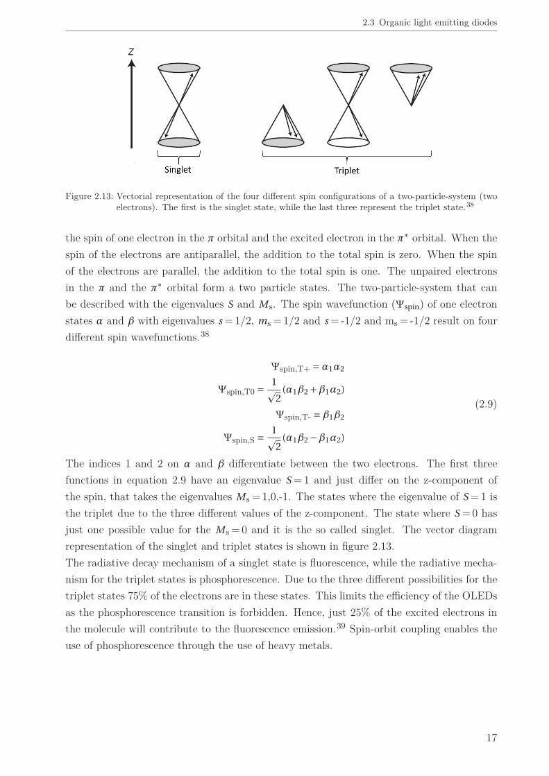
Figure 2.13: Vectorial representation of the four different spin configurations of a two-particle-system (twoelectrons). The first is the singlet state, while the last three represent the triplet state.38
the spin of one electron in the π orbital and the excited electron in the π∗ orbital. When thespin of the electrons are antiparallel, the addition to the total spin is zero. When the spinof the electrons are parallel, the addition to the total spin is one. The unpaired electronsin the π and the π∗ orbital form a two particle states. The two-particle-system that canbe described with the eigenvalues S and M s. The spin wavefunction (Ψspin) of one electronstates α and β with eigenvalues s = 1/2, ms = 1/2 and s = -1/2 and ms = -1/2 result on fourdifferent spin wavefunctions.38
Ψspin,T+ =α1α2
Ψspin,T0 =1p2
(α1β2 +β1α2)
Ψspin,T- =β1β2
Ψspin,S = 1p2
(α1β2 −β1α2)
(2.9)
The indices 1 and 2 on α and β differentiate between the two electrons. The first threefunctions in equation 2.9 have an eigenvalue S = 1 and just differ on the z-component ofthe spin, that takes the eigenvalues M s = 1,0,-1. The states where the eigenvalue of S = 1 isthe triplet due to the three different values of the z-component. The state where S = 0 hasjust one possible value for the M s = 0 and it is the so called singlet. The vector diagramrepresentation of the singlet and triplet states is shown in figure 2.13.The radiative decay mechanism of a singlet state is fluorescence, while the radiative mecha-nism for the triplet states is phosphorescence. Due to the three different possibilities for thetriplet states 75% of the electrons are in these states. This limits the efficiency of the OLEDsas the phosphorescence transition is forbidden. Hence, just 25% of the excited electrons inthe molecule will contribute to the fluorescence emission.39 Spin-orbit coupling enables theuse of phosphorescence through the use of heavy metals.
17
2 Fundamentals of organic semiconductors
2.3.3 OLED characterization
The electromagnetic radiation emitted by an OLED can be characterized in terms of phys-ical quantities (i.e. number of photons, photon energy, optical power commonly known as“radiant flux”). However, these units do not consider the human eye’s perception of light.For example, if an OLED has a high emission of photons in the infrared, the emitted opticalenergy could be high. This would not matter to the human eyes as they cannot detect lightin the infrared regime. Therefore, different units that consider the perception of the humaneye are needed. These units are called photometric units.40
• The luminous intensity (I v), represents the intensity of an optical source, as perceivedby the human eye. Its units are candela (cd), which is a base unit of the InternationalSystem of Units. A candela is defined as: the luminous intensity, in any given directionof a source that emits monochromatic radiation of frequency 540 x 1012 hertz and thathas a radiant intensity in that direction of 1/683 watt steradian-1.41
• The luminous flux (Φ), represents the light power of a source as perceived by the hu-man eye. The unit of luminous flux is the lumen (lm) and it is defined as:the luminousintensity, in any given direction of a source that emits monochromatic radiation of fre-quency 540 x 1012 hertz and that has a radiant intensity in that direction of 1/683 watt.The lumen is an SI unit derived from the candela. One candela is equivalent to onelumen steradian-1 or cd = lm sr-1. OLEDs are considered lambertian sources. A lam-bertian source emits light uniformly in all directions. Hence the luminance of an OLEDcan be calculated by:
L = Φ
Aπ(2.10)
• The illuminance is the luminous flux incident per unit area. The unit of illuminanceis the lux = lm m-2. It is used to characterize the necessary illuminance in differentenvironments, i.e. office desk lighting should have a minimum of 500 lux.
• The luminance (L) of a surface source is the ratio of the luminous intensity emitted ina certain direction (measured in cd) and the projected surface area(measured in m2).
• The current efficiency (ηc) is also an important performance parameter. It is calculatedby dividing the luminance (L) by the current density (J).
ηc = L
J(2.11)
• The power efficiency (η) is given by the ration between the luminous flux and theelectrical power (P).
η= ΦP
(2.12)
18

2.3 Organic light emitting diodes
2.3.4 Upscaling of OLEDs
Similar to the case of organic solar cells, the resistance of the transparent electrode has asignificant impact on the device performance when it is upscaled. In OLEDs it is even morerelevant as the high sheet resistance can lead to a voltage loss in the device that is translatedinto inhomogeneous luminance.42 This high sheet resistance leads also to lower efficiency asthe current necessary to light the devices increases with the area. Initial efforts to integratehighly conductive metal grids or bus bars have been explored to solve this problem.43–45
Slawinsky et al. tested different grid configurations and increased the homogeneity of a12 x 12 cm2 device.44 However, the bus bars and grids remain visible hence affecting thehomogeneity of the device.Another approach to reduce the current on the device, and consequently the resistive losses,is the use of tandem architectures. The tandem architectures allows the production of morethan one photon per electron-hole pair.46–51 This reduces the current and doubles the voltage,hence reducing the power losses when the device is upscaled.The concept of monolithic connections (Figure 2.11) has also been explored for OLEDs. Theindividual OLED size is limited and therefore the current is reduced. As in the case of thetandem option, the driving voltage increases with the number of individual units that areconnected. Duggal et al. demonstrated the feasibility of this approach in OLEDs, enhancingthe lifetime of the devices as the number of faulty devices decreased.52 Analogous to thecase of organic solar cells, the area between P1 and P3 does not emit light and therefore,should be reduced as much as possible. This concept is further explored in this thesis.
19


3 Fabrication and characterization
This chapter covers the different coating and characterization techniques used in this work.Section 3.1 describes the preparation process of the samples, from the cleaning of the substratesto the layer application processes. The cleanroom environment where the experiments tookplace is also described in this section. Section 3.2 describes the different characterizationmethods used in this work. Finally, section 3.3 describes the laser setup used for the ablationexperiments elaborated under the scope of this work.
3.1 Sample preparation
3.1.1 Substrate preparation
Both rigid glass and flexible Polyethylene terephthalate (PET) substrates were used in thescope of this work. Indium tin oxide (ITO) was used as semitransparent electrode in bothglass and PET substrates. The ITO was structured by etching for 10 minutes in a bathof hydrochloric acid (37% concentration). The substrates were subsequently cleaned withacetone and isopropanol in an ultrasonic bath (10 min each) and dried using nitrogen. Thesubstrates were then exposed to oxygen plasma for 2 minutes to remove any organic residues.
3.1.2 Layer application from solution
Two main solution coating methods were used to manufacture the devices investigated inthis work: spincoating and doctor blading.
• Spincoating is one of the most reliable techniques to apply layers from solution onlaboratory scale. It allows the formation of highly reproducible films and it can coatsubstrates up to 30 cm2. The typical spincoating process involves the application ofa liquid to a substrate followed by acceleration of the substrate to a chosen rotationalspeed. The process can involve different steps, each with its own speed, time lapseand acceleration. The angular velocity of the substrate results in ejection of mostof the solution, leaving just a thin-film on the substrate. The thickness depends onthe rotational speed, viscosity, volatility, molecular weight and concentration of thesolutions. The film thickness d can be empirically estimated from the relationship.53
d = kωα (3.1)
21

3 Fabrication and characterization
Where ω is the angular velocity and k and α are constants related to the physicalproperties of the solution. Spincoating has the disadvantage that most of the solutionis wasted and it is not compatible to roll-to-roll production as the substrates need tobe handled individually. All spincoating was performed in a glovebox under nitrogenatmosphere. The spincoater used for this work was located at the Light TechnologyInstitute (LTI).
• Doctor blading is a coating technique that has the advantage of producing less waste(less than 5%). The technique works by placing a blade at a fixed distance from thesubstrate surface that has to be coated. Typically, the gap is between 10 and 500 µm.The solution is then deposited in front of the blade (Figure 3.1). The blade is movedat a constant or variable speed pushing the solution over the substrate. The variablespeed helps to compensate for the lack of material at the end of the substrate, henceproducing more uniform layers. Some doctor blading systems also have a temperaturecontrolled plate that helps to regulate the drying process of the film.53
The final wet thickness should be around half of the blade height. The final dry thick-ness depends on the concentration of the solution. The speed of the blade also playsan important role. The final dry thickness can be calculated from the the empiricalrelationship:55
d = cv23 (3.2)
Where c is an empirical factor and v is the speed of the blade. The main advantagesof doctor blading over spincoating is that almost no material is lost, reducing thematerial use. Another advantage is that doctor blading is easily transferable to roll-to-roll process as it is similar to the knife-over-edge coating. It also has similarities toslot-die coating.
The main drawback of the doctor blading technique is the possible inhomogeneity ofthe film. This homogeneity is largest in the beginning and in the end. This can bepartially compensated with the use of an accelerated process. Another disadvantage
Figure 3.1: Doctor blading system. The solution is placed in front of the blade. The blade then forms thelayer by pushing the solution through its gap.54
22

3.2 Characterization methods
compared with spincoating is that the layer has a slower drying process that can leadto a different morphology of the film.
The doctor blading system (ZA A 2300, Zehntner GmbH Testing Instruments) usedduring this work was located at the Light Technology Institute. It was used both undernitrogen and ambient atmosphere. Two different applicators were used, the Universal-applicator (ZUA 2000 Universal-Applicator, Zehntner GmbH Testing Instruments) anda cylindrical applicator with different gap heights.
3.1.3 Thermal evaporation layer application
The hole transport layer and silver electrode were deposited using an evaporation machine(Spectros, Kurt J. Lesker Company LTD.) located at the LTI. The evaporation takes placeunder high vacuum of 10-6 bar. The evaporation machine has a three state pump systemto reach this low pressure in approximately 15 minutes. The sample is then placed in arotatory stage to guarantee a homogeneous deposition of the material. The layer thicknessis measured through a quartz crystal. The crystal detects the change of frequency due to thechange of mass. Two different crystals are used, one for dielectrics and one for metals. Thematerials are evaporated from two different sources, were they are heated using an electriccurrent.
3.1.4 Cleanroom environment
Due the thin-film nature of OPV and OLEDs, particles on the atmosphere can greatlydamaged them, creating shunts and shorts on the devices. Therefore, the devices weremanufactured in the cleanroom in the LTI. The cleanroom is divided in three differentrooms each with a different cleanroom class. The substrates were cut and etched in the firstroom with a cleanroom class of 100,000. Both spincoating and doctor blading systems werelocated in a room with yellow lighting and a cleanroom class of 1000 for the process underambient atmosphere. For the processing of oxygen and water sensitive materials, the layerswere deposited and characterized inside gloveboxes under nitrogen atmosphere.
3.2 Characterization methodsThis section describes the different characterization methods required to measure the elec-trical and optical properties of OPV and OLEDs. The methods to characterize the laser andthe laser structured lines are also described.
3.2.1 Topography characterization
One of the main needs for this work was to characterize the laser structured lines processes.A 3D confocal profiler was the main tool used for this purpose. An atomic force microscopeand scanning electron microscope were also used.
23

3 Fabrication and characterization
Figure 3.2: Confocal microscope working principle. The light coming from a light source is reflected using adichroic mirror. The light that is reflected from the focal plane reaches the imaging system (redline) while the light that is reflected from other surfaces that are not in focus is blocked by thepinhole (blue line).
• A 3D profiler with confocal and white light interferometry functions (Sensofar Neox)was mainly used for the characterization of the structured layers. The confocal optionwas mostly used in this work. The profiler has two different objectives for confocalmicroscopy with two different amplifications 20x (NA=0.45) and 150x (NA=0.95), bothfrom Nikon. It has two different light sources, blue and white. Confocal microscopyis a non contact 3D profiling method. Figure 3.2 shows the working principle. Lightcomes from a light source and it is focused. The focused light is reflected using adichroic mirror. The light then is focused on the sample through an objective. Thelight that comes from the focal plane will be detected by the imaging system. Theunfocused light (blue line) is blocked by a pinhole. This way the illumination and theobservation are focused. In order to perform a 3D scanning, several pictures of thisfocused images are taken by changing the position in the Z-axis.56 The Sensofar Neoxcan move with small steps of 100 nm. The system was also used to measure the size ofthe active areas of the solar modules and the width of the inactive areas. The confocalmicroscope is located at the Material Research center for Energy Systems (MZE).
• An atomic force microscope (AFM, Dimension Icon, Bruker) was used for in-depthmeasurements of the laser structured layers. The atomic force microscope works usinga sharp tip that is attached to a cantilever (Figure 3.3). A laser beam is reflected onthis cantilever to a photo diode. The forces due to the surface variations will deflectthe cantilever by attracting the sharp tip. The photodiode detects the deflection ofthe cantilever by measuring the movement of the laser. All measurements done inthis work were done in tapping mode. In this measurement mode, a piezo excites thecantilever to vibrate near its resonance frequency above the surface. A change in the
24

3.2 Characterization methods
Figure 3.3: AFM tapping mode working principle. The cantilever scans the surface and detects the heightvariations. A laser is reflected on the cantilever. The height variations are measured by detectingthe laser position variations.58
external potential, will alter the phase difference between the driving force and thecantilever oscillation amplitude. Both quantities can then be used as feedback signal.This method has the advantage that the tip barely touches the surfaces decreasing thetip wear.57
• A scanning electron microscope (FE-SEM, FEI Nova NANOSEM) was used for furtheranalysis of the laser structured lines. The device was used in low vacuum with a gaseousanalytical detector (GAD) and a low-vacuum detector (LVD). An electron beam scansthe surface of the sample, releasing secondary electrons from the surface of the sample.The secondary electrons are then detected by a sensor, registering different levels ofbrightness. To analyze the edge of the laser structured samples, they were brokenusing liquid nitrogen. The samples were then measured using a tilt angle of 70°.
3.2.2 Optoelectrical characterization
To evaluate the performance of the devices and the absorption characteristics of the layers,different measurement techniques were used.
• A UV-VIS-NIR spectrometer (Cary5000 Agilent Technologies) was used to determinethe spectral linear absorption of the different layers. Transmission (T) and reflexion(R) were measured using an integrating sphere. For the transmission measurements,the substrates were placed in front of an integrating sphere while for the reflexionmeasurements, they were placed behind. Absorption (A) was then calculated usingthe following relation:
A = 1−R −T (3.3)
• An integrated, home built OLED characterization system (OCS) was used to measurethe electrical and optical characteristics of the OLEDs. The system is in a nitrogenatmosphere inside a glovebox in the LTI. The sample is placed on a XY stage. There
25

3 Fabrication and characterization
are in total eight pins that were used to connect the different devices. A voltage isthen applied to the device and the current density J of the device is recorded. Theemitted light is measured through a fiber that is connected to a spectrometer (EEP2000, StellarNet). The measuring position is calibrated using a laser. The calibratedspectrum (φe(λ)) is recorded by the spectrometer. The luminous flux (φ) is thencalculated using the following relation:
φ= Km
∫ λ2
λ1φe(λ)Vλ(λ)dλ (3.4)
For the OLED modules, the measuring position was set next to the monolithic con-nection to measure the whole OLED module. The OCS is located in the cleanroom atthe LTI.
• A solar simulator was used to evaluate the performance of the solar cells and mod-ules. The solar simulator has a Xenon lamp that simulates the ASTM AM 1.5 solarspectrum. Different sample holders were used depending of the kind of substrate. Forthe 16 x 16 mm2 a holder with 8 pins was used, allowing the subsequent measure offour solar cells on one substrate. For the larger modules, crocodile clamps were used.The voltage was applied using a Keithley Source Measure Unit (SMU). The current ismeasured, recorded and divided by the photoactive area of the device to calculate thecurrent density. The software automatically determines the key performance parame-ters, V oc, J sc, PCE and F F . Before the measurements, the system is calibrated usinga reference cell from Newport.
3.3 Laser ablation setupThe femtosecond laser ablation setup is composed of three main parts and it is located atthe LTI:
• Ultrashort pulse amplifier (Libra, Coherent)
• Ultrafast optical parametric amplifier (OPerA Solo, Coherent)
• Workstation (µFAB, Newport)
The three parts are installed on top of an optical table (Newport) at the LTI. The beamis routed from the laser source to the workstation using different routing mirrors that arechanged depending on the selected wavelength. Depending on the laser source, the positionof the routing mirrors is modified. The main characteristics of each part are described below.
3.3.1 Ultrashort pulse amplifier (Libra)
The Libra is a chirp amplified laser that comprises:
26

3.3 Laser ablation setup
Figure 3.4: Libra optical bench assembly.The four main components of the Lbra are depicted.59
• Vitesse modelocked femtosecond laser (seed laser)
• Evolution Q-switch laser (pump laser)
• Synchronization and delay generator (SDG)
• Beam compressor/stretcher
• Regenerative amplifier
• Closed loop cooling chiller
The seed laser, the pump laser, the beam compressor/stretcher are all enclosed in the Libraoptical bench assembly (Figure 3.4).
• The Vitesse laser works as the seed laser for the regenerative amplifier. It is composedof a modelocked Ti:Sapphire laser that is pumped by a continuous-wave diode-pumpedgreen laser (Verdi Coherent).
27

3 Fabrication and characterization
Table 3.1: Libra output beam specifications.
Parameter Value
Central wavelength (nm) 800Average power (W) 3.6Pulse energy (mJ) 0.72
Spatial mode TEMoo, M2 < 1.3Polarization Linear horizontal
Repetition rate (Hz) 5000Pulse length (fs) 90
• The Evolution is a diode-pumped second harmonic Q-switched laser that providesthe pump power for the regenerative amplifier. It operates at λ= 527 nm and has arepetition rate of 5000 Hz.
• The regenerative amplifier amplifies one of the pulses of the seed laser using the pumppower. The regenerative amplifier employs two Pockels cells. The first Pockels cell letsthe pulse in the cavity after a certain number of amplification round (approximately8-10), the second Pockels cell is activated letting the pulse out of the amplifier. Thepulse is then send to the compressor. The amplification takes process in a Ti:Sapphirecrystal where both seed and pump beam meet. The Pockels cells are regulated by theSDG. The whole regenerative amplifier is actively cooled by a chiller.
• The stretcher and compressor work with gratings. The compressor has a fine adjust-ment tool that helps to optimize the compression level of the output pulses. The beamtakes several passes on the gratings to achieve the adequate stretching/compressionlevel.
The output beam of the Libra has the characteristics depicted in table 3.1.
3.3.2 Ultrafast Optical parametric amplifier (OPerA Solo)
The ultrafast optical parametric amplifier (OPerA Solo) is a two-stage parametric amplifierof white-light continuum. The OPerA Solo is composed of the following subunits:
• Pump delivery and splitting optics (PO)
• White-light continuum generator (WLG)
• Pre-amplifier (PA1)
• Signal beam expander collimator
• Amplifier
28

3.3 Laser ablation setup
Table 3.2: OPerA Solo wavelength regimes.
Regime Wavelength Range (nm)
Idler 1650-2600Signal 1175-1600
Second harmonic idler (SHI) 825-1150Second harmonic signal (SHS) 580-800
Sum frequency idler (SFI) 540-600Sum frequency signal (SFS) 480-530Fourth harmonic idler (FHI) 400-480
Fourth harmonic signal (FHS) 290-400
The OPerA Solo installed in the LTI includes the optics necessary to work with the differentwavelengths (table 3.2).The output beam of the Libra is used as input beam. The beam is directed through routingmirrors to a beam splitter (BS1). Approximately, 4 % of the power is directed to the pre-amplifier stage (PAS). The bulk of the beam is directed to the power amplification stage.The small part of the beam is again split (BS2), one part will be used for the white-lightcontinuum generation (WLC, approximately 1-3 µW) and the second part is used as thepump beam (30-70 µW) for the pre-amplification stage. The WLC is generated in a sapphirecrystal plate (SC). The WLC and the pump beam are overlaped non-collinearly in the firstnon linear crystal (NC1) where, parametric amplification takes place. The residual pumpand idler are blocked using a beam blocker (BB) while the signal is directed to the poweramplification stage. In the power amplification stage the signal and the remaining of thepump are overlapped collinearly and non-collinearly in the second non-linear crystal (NC2).This results in collimated signal and idler beams. A dichroic mirror (DM) is used to separatethe signal and the idler. If the signal is to be used, it is directed to the output of the OPerASolo using a routing mirror (SM). In case the idler has to be used, the idler mirrors (IM1and IM2) are installed. This mirrors are magnetic and have a fixed position. When installedthey also block the signal beam. The optics for the generation of the second harmonic,sum frequency and fourth harmonic are installed after the position of the idler mirrors. Asimplified schematic of the process is shown in figure 3.5.The wavelength adjustments are done by changing the delay of the beams in the pre-ampliferand amplifier stages, and the crystal angles. This is controlled by a computer software. Thecomputer software also controls the output wavelength. Besides the installation of the IM1and IM2, different beam splitters need to be installed, depending on the operation regimethat is chosen.The pulse energy varies depending on the chosen wavelength. Figure 3.6 shows the differentpulse energies at the output of the OPerA Solo for the different wavelengths. The highestefficiency of the system is 22.8% at λsignal = 1300 nm and λidler = 2066 nm. The beam willcome out through one of the four different outputs of the OPerA Solo depending on theregime that is used.
29

3 Fabrication and characterization
Figure 3.5: Simplified schematic OPerA Solo. The input beam is split (BS1). Around 4% is directed to thepre-amplifier while the bulk is directed to the amplifier. In the pre-amplifier the beam is splitagain (BS2). The smaller part is used to a generate white-light continuum (WLC) depicted as awhite line. The larger part is used as the preamplifier pump. Both beams meet non-collinearlyat the first non-linear crystal (NC1). Parametric amplification takes place. The signal beamis then directed to the amplifier while the idler and the rest of the pump are blocked with abeam blocker (BB). The signal meets the bulk of the input beam in the second non-linear crystal(NC2). Signal and idler beams are produced by the parametric amplification. A dichroic mirrorseparates the signal and the idler. In case of use of the idler, magnetic mirrors (IM1 and IM2) areinstalled. The mirrors block the signal beam. In case of using the signal the mirror SM directsthe beam to the output.
Figure 3.6: OPerA Solo pulse energies for different wavelengths and different regimes.
To monitor the output power of the OPerA Solo, a power meter (PS19, Coherent) with aresolution of 10 µW was used. During the scope of this work the wavelength range fromλ= 360 nm to λ= 750 nm was used.
30

3.3 Laser ablation setup
Figure 3.7: µFAB schematic showing the laser beam path from the entrance of the µFAB to the final focusingobjective.
3.3.3 Workstation (µFAB, Newport)
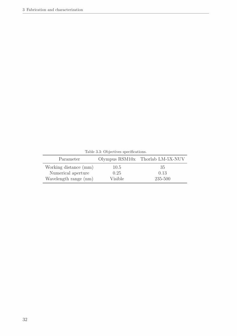
The final part of the laser setup is the worktstation (µFAB, Newport). After the beamenters the workstation, the beam is attenuated using a 1/2 waveplate (HWP) combinedwith a Glan-laser polarizer (P). The HWP is attached to a software controlled rotatorystage. The polarizer lets a certain amount of light pass depending on the rotation angle ofthe HWP. Then the beams goes to a beam splitter (BS). A fraction of the beam is redirectedto a power head (PH, Newport 918 DUV 0D3R). This fraction is used as reference to monitorthe power on the sample. The beam goes to a mechanical shutter (S). After the shutter, thebeam goes to a quarter waveplate (QWP) where the polarization is changed to circular. Thebeam then goes to a telescope for final collimation before being directed to the objective(OL). The sample is placed on an XYZ motorized stage. A CMOS camera is used as apositioning reference on the sample (Figure 3.7). The relationship between the power onthe sample and the reference power changes with different wavelengths. Therefore a powerrelationship is measured on the sample position using a different power meter (USB UV/VIS,Coherent) in combination with the one on the workstation.Two different objectives were used during this work, one for the visible and one for the UVregime, mainly at λ= 360 nm. The specifications are given in table 3.3.
31
3 Fabrication and characterization
Table 3.3: Objectives specifications.
Parameter Olympus RSM10x Thorlab LM-5X-NUV
Working distance (mm) 10.5 35Numerical aperture 0.25 0.13
Wavelength range (nm) Visible 235-500
32
4 Laser principles
This chapter explains the basic working principles of a laser. Section 4.1 covers the theorybehind the different laser sources used in this work such as modelocked, q-switching and chirpamplifiers. Section 4.2 covers the parametric amplification and non linear processes used inthe OPerA Solo.
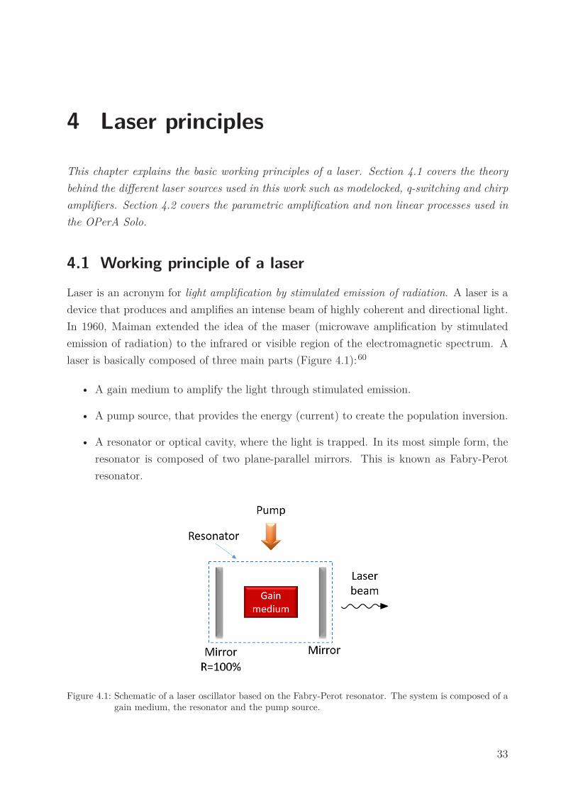
4.1 Working principle of a laserLaser is an acronym for light amplification by stimulated emission of radiation. A laser is adevice that produces and amplifies an intense beam of highly coherent and directional light.In 1960, Maiman extended the idea of the maser (microwave amplification by stimulatedemission of radiation) to the infrared or visible region of the electromagnetic spectrum. Alaser is basically composed of three main parts (Figure 4.1):60
• A gain medium to amplify the light through stimulated emission.
• A pump source, that provides the energy (current) to create the population inversion.
• A resonator or optical cavity, where the light is trapped. In its most simple form, theresonator is composed of two plane-parallel mirrors. This is known as Fabry-Perotresonator.
Figure 4.1: Schematic of a laser oscillator based on the Fabry-Perot resonator. The system is composed of again medium, the resonator and the pump source.
33

4 Laser principles
Figure 4.2: Absorption, spontaneous emission and stimulated emission in a two-level system with energiesE2 and E1 .61
4.1.1 Light matter interaction
As discussed in chapter 2, light can be absorbed and emitted by matter with the exci-tation/decay of an electron. These two processes are called absorption and spontaneousemission. A third process is the so called stimulated emission of light. This process will bediscussed in more detail below (figure 4.2)61:
• Absorption of a photon with energy hv=E2-E1. E2 and E1 are the energy of twodifferent levels in the system where the light interaction occurs. The absorption causesthe excitation of a particle from E1 to E2.
• Spontaneous emission of an emitted photon with an energy hv . This is caused by thedecay of a particle from E2 to E1. The name spontaneous emission originates from themoment of emission, when the polarization and the direction of the light is random.This process is responsible for the fluorescence of excited media.
• When an incoming photon induces a resonant transition from E2 to E1, stimulatedemission of a second photon of energy hv occurs. As it is resonant process both photonsare identical. This effect allows the amplification of light which is fundamental for alaser.
4.1.2 Population inversion
Laser amplification occurs, if less light is absorbed than emitted. This is commonly referredto as effective gain. The equation for the effective gain is related to the effect of the lightabsorption described by the Lambert-Beer law:61
I (z,λ) = I (0,λ)e−α(λ)z (4.1)
The absorption coefficient (λ) is proportional to the number density N1 that describes thenumber of entities in state E1.
α(λ) =σa(λ)N1 (4.2)
The proportionality constant σa(λ) is the absorption cross section. The stimulated emission(amplification) of light is:
34

4.1 Working principle of a laser
I (z,λ) = I (0,λ)eγ(λ)z (4.3)
Similar to the previous case the emission coefficient γ(λ) is proportional to the numberdensity N 2 that describes the number of entities in state E2.
γ(λ) =σe(λ)N2 (4.4)
The proportionality constant σe(λ) is the emission cross section. When combining bothprocesses, the total evolution of the spectral density is:
I (z,λ) = I (0,λ)e(σe(λ)N2−σa(λ)N1)z (4.5)
And the total gain of the system is:
G(z,λ) = I (0,λ)
I (0,λ)e(σe(λ)N2−σa(λ)N1)z (4.6)
To obtain a net amplification of light, G>1 is needed, hence N 2 needs to be larger than N 1.This is the so called population inversion, meaning that more entities populate the upperenergy level E2 than the lower energy level E1. In thermal equilibrium, the populationdensity relation between the two levels is directly given by the Boltzmann distribution:
N2N1
= e− hv21
kBT (4.7)
It is not possible to achieve population inversion in thermal equilibrium, ergo an excitationsource is required to excite the two level system (Figure 4.2). The ratio of N 2 and N 1 canbe described using the Einstein coefficients B12 and A21 in steady state:
N2N1
= B12u(v)
B12u(v)+ A21< 1 (4.8)
Where u(v) is the radiation density of the excitation source. As seen in equation 4.8, aneffective gain is not feasible, hence preventing the laser process in a two-level steady statesystem. An attainable way to achieve the population inversion is to add a third level to thesystem. The third level causes that absorption and emission occur at different wavelengths.When a three-level system is pumped, the population changes from level E1 to level E3 witha rate W p. This brings an entity to the top level E3. A fast decay from the level E3 tothe level E2 occurs, keeping the population of level E3 close to zero. When the absorption,the emission, and the spontaneous emission, plus the decay from level E3 to level E2 areconsidered, the change of N 2 in time is:
d N2d t
=WpN1+W12N1−W21N2− A21N2 (4.9)
Considering steady state. The ratio between N 2/N 1 is given by:
35

4 Laser principles
N2N1
= Wp+W21A21W21
(4.10)
Therefore, it is possible to have a positive gain and population inversion in a three levelsystem. However, this system has low efficiency as it has to compensate for the spontaneousemission rate. This leads to a high threshold to initiate the laser process.To increase the efficiency, a four-level system is used. This principle follows the same ideathat allowed the population inversion from the two-level system to the three-level system.It increases the efficiency by reducing the need of a high upper level population in N 2. Thefour-level system is represented in figure 4.3:In the four-level system a pump is used to create an excitation to the level E4. Similar tothe three-level system a fast decay is necessary from the level E4 to the level E3 keeping thepopulation of level E4 close to zero. Also there is a fast decay from level E2 to level E1. Theenergy separation between E2 and E1 needs to be sufficient to prevent thermal populationof E2. This keeps the population of level E2 close to zero. The population of N 3 consideringthe aforementioned processes is then given by:
N3 =Wp
Wp+W32+ A32+ A31(4.11)
This leads to a population inversion of N 3 with respect to N 2, that has a population closeto zero. The population inversion is present even with a low population accumulation inlevel three, hence decreasing the necessary pumping power and increasing the efficiency ofthe system.Although the Ti:Sapphire laser that is mainly used in this work has a vibronic state config-uration, its working principle can be approximated as a four-level system as shown in figure4.4.
Figure 4.3: Four-level laser system and the light interactions within.61
36

4.1 Working principle of a laser
(a) (b)
Figure 4.4: (a) Vibronic states in a Ti:Sapphire laser. (b) Four-level energy approximation of a Ti:Sapphirelaser.62
4.1.3 Feedback system
In the previous section, the necessary conditions to create population inversion are studied.As it is shown in figure 4.1 one of the main components of a laser is the resonator. Thisresonator is also known as laser cavity. One simple example of a resonator is the Fabry-Perotresonator that is composed of two different mirrors with different reflections. This allow us toreflect the amplified radiation back and forth in the gain medium. As seen in figure 4.1, oneof the reflective mirrors has 100% reflection while the other mirror has less than 100%. Thisone is known as output coupler (OC mirror) as it allows the beam to leave the resonator.61
4.1.4 Types of lasers
Lasers can be classified in two main groups:60
• Continuous wave lasers (CW): this type of lasers has a continuous flow of outputenergy, with small or no time variations. Some examples are: HeNe and Ar-ion lasers.
• Pulsed lasers: this type of lasers has a variation in the flow of energy output, asthe energy is emitted in pulses with an specific time range that can vary from µs tofs. Pulsed lasers are used in this work. Typical example are the Nd:YAG and theTi:Sapphire.
Two of the most common methods to generate pulsed beams are Q-switching and modelock-ing, both are described below.
4.1.5 Q-Switching
Q-switching is a technique that uses the gain medium as an energy container. The energy isaccumulated by not letting the beam escape through the outcoupling mirror. This creates ahigh level of population inversion that is far above the threshold for a CW operation of thelaser. When the outcoupling mirror is activated, the stored energy is released in the form of
37

4 Laser principles
Figure 4.5: Q-Switching process description. The energy of the pump is accumulated in the gain medium.The outcoupling mirror is opened, and with a certain delay a pulse with duration tp is released.63
a pulse of light after some delay. The pulse duration tp is usually short in the range of ns.The peak power of this pulse is far greater than the normal peak power of a CW laser.63
This process is depicted in figure 4.5. The Evolution is a Q-switching laser used in this work.
4.1.6 Modelocking
The short pulses generated using the Q-Switching process are limited to 20 ns. The limitationis due to the size of the resonator. To produce even shorter pulses in the ps and fs regime,mode-locking is used. The technique uses the fact that even lasers emit light in a certainbandwidth ∆υ. Therefore, the laser oscillates in the gain medium with a large number oflongitudinal modes. The process induces the locking of the different modes that are inside thegain medium into one fixed phase. This is possible because all the frequencies are multiplesof the same fundamental frequency. This allows the production of ultrashort pulses in therange of tens of fs.64 65 61 The pulse width is inversely related to the bandwidth of the lasersource by:
Tp ≈ 1
∆υ(4.12)
Hence, a prime gain medium for mode-locking is Ti:Sapphire that has a ∆υ = 1.1 x 10¹⁴ Hz.This is the type of gain medium inside the Vitesse, that is the laser used as seed inside theLibra.
38
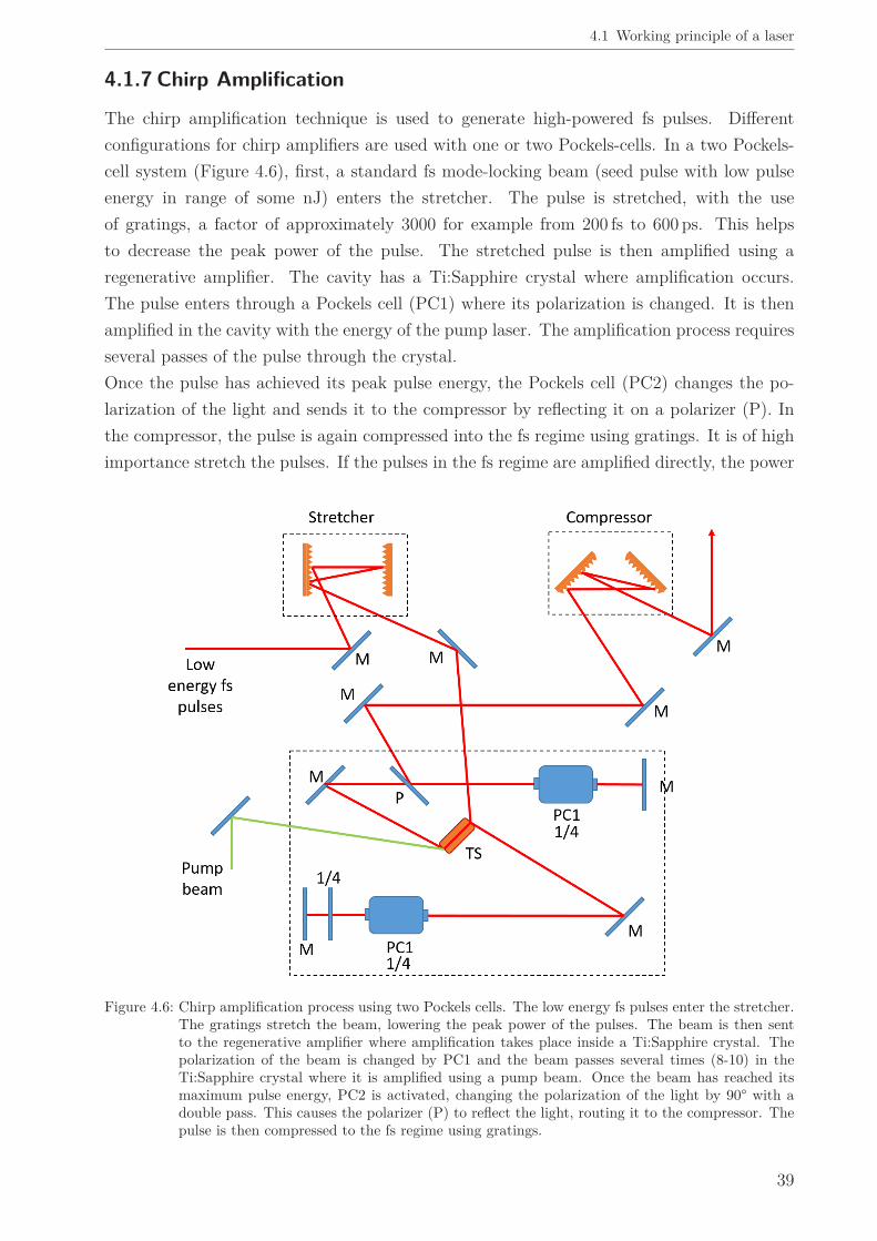
4.1 Working principle of a laser
4.1.7 Chirp Amplification
The chirp amplification technique is used to generate high-powered fs pulses. Differentconfigurations for chirp amplifiers are used with one or two Pockels-cells. In a two Pockels-cell system (Figure 4.6), first, a standard fs mode-locking beam (seed pulse with low pulseenergy in range of some nJ) enters the stretcher. The pulse is stretched, with the useof gratings, a factor of approximately 3000 for example from 200 fs to 600 ps. This helpsto decrease the peak power of the pulse. The stretched pulse is then amplified using aregenerative amplifier. The cavity has a Ti:Sapphire crystal where amplification occurs.The pulse enters through a Pockels cell (PC1) where its polarization is changed. It is thenamplified in the cavity with the energy of the pump laser. The amplification process requiresseveral passes of the pulse through the crystal.Once the pulse has achieved its peak pulse energy, the Pockels cell (PC2) changes the po-larization of the light and sends it to the compressor by reflecting it on a polarizer (P). Inthe compressor, the pulse is again compressed into the fs regime using gratings. It is of highimportance stretch the pulses. If the pulses in the fs regime are amplified directly, the power
Figure 4.6: Chirp amplification process using two Pockels cells. The low energy fs pulses enter the stretcher.The gratings stretch the beam, lowering the peak power of the pulses. The beam is then sentto the regenerative amplifier where amplification takes place inside a Ti:Sapphire crystal. Thepolarization of the beam is changed by PC1 and the beam passes several times (8-10) in theTi:Sapphire crystal where it is amplified using a pump beam. Once the beam has reached itsmaximum pulse energy, PC2 is activated, changing the polarization of the light by 90° with adouble pass. This causes the polarizer (P) to reflect the light, routing it to the compressor. Thepulse is then compressed to the fs regime using gratings.
39

4 Laser principles
would be too high for the crystal damaging it. This is the amplification process used insidethe Libra, the fs laser system used in this work.
4.2 Wavelength tuning
4.2.1 Optical parametric amplification
The heart of the system used in this thesis is an optical parametric amplifier. This sectionwill briefly explain the theory behind its working principle.In an optical parametric amplification the input includes two beams, the signal beam and thepump beam. In the output, a new beam that is called the idler is obtained.66 The followingequations gives the energy conservation in a parametric amplification process:
ωp =ωs+ωi (4.13)
The pump beam frequency (ωp) equals the addition of the signal (ωs) and the idler (ωi)beams’ frequencies. This is depicted in figure 4.7.The difference between the second harmonic conversion and the parametric amplification isthat the signal beam is indeed amplified using this process and not only converted to theidler. This amplification comes from the conversion of some of the pump beam photons intosignal and idler photons.The energy condition mentioned in equation 4.13 allows the generation of any frequencysmaller than ωp. The frequency ωs is controlled by the phase matching condition ∆k = 0.The phase matching can be modified either by changing the angle of the non-linear crystal orby changing its temperature.66 The first option is the one used in both amplification stagesinside the OPerA Solo.
4.2.2 Sum-frequency generation
The sum-frequency generation is an up-conversion process where two beams with frequenciesω1 and ω2 are combined to obtained a higher energy beam with frequency ω3 (Figure 4.8).66
Figure 4.7: Frequency relationship in a parametric amplification between the pump, signal and idler beams.
40

4.2 Wavelength tuning
Figure 4.8: Frequency relationship in a sum-frequency interaction.
The process is used using Nd:YAG pulses at λ1 = 1064 nm, combined with its own secondharmonic at λ= 532 nm to generate UV pulses at λ= 355 nm.A special case of the sum frequency generation is the second harmonic generation in whichω1 and ω2 are equivalent and ω3 results in a frequency doubling. If this process is repeated,the fourth harmonic is obtained.These processes sum-frequency, second harmonic and fourth harmonic are used in the OPerASolo. The OPerA Solo applies the aforementioned process to the signal and idler beamsallowing us to achieve different wavelengths.
41


5 Laser processing
This chapter covers the fundamentals of laser processing. The interaction of lasers withmatter is a complex process that depends on the type of material, the laser wavelength, thelaser intensity, the pulse length etc. Section 5.1 gives a short introduction to the matter-laserinteraction processes. Section 5.2 covers the principle of nanosecond laser ablation. Section5.3 covers the principles of the ultrashort pulse laser ablation, the methods to determine thelaser threshold fluence and the pulse overlap.
5.1 Laser matter interactionThe interaction between the laser beam and the matter depends on different factors. Onthe laser side, the parameters that play an important roll are: type of beam (continuous orpulsed), wavelength, intensity, coherence, polarization, beam shape and angle of incidence.On the material side, the chemical composition and the microstructure will determine theinteraction with the laser beam.67 Depending on the laser intensity, different interactionsmay occur. An overview is depicted in figure 5.1.
Figure 5.1: Overview of different laser-matter interactions depending on the laser intensity. The types oflasers to achieve this interactions are indicated.67
43
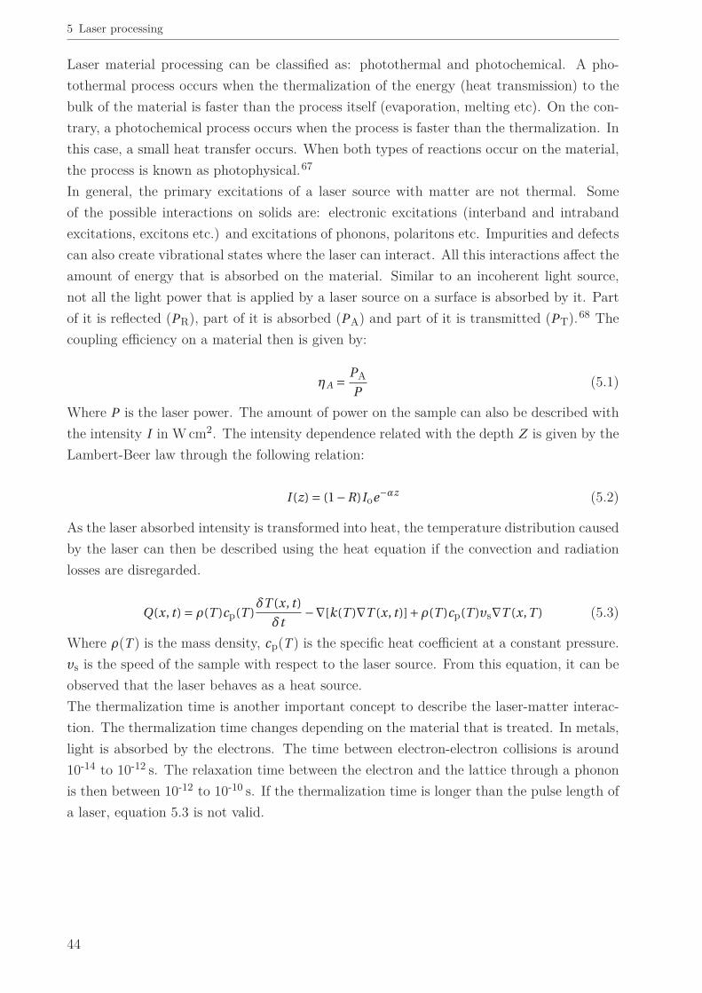
5 Laser processing
Laser material processing can be classified as: photothermal and photochemical. A pho-tothermal process occurs when the thermalization of the energy (heat transmission) to thebulk of the material is faster than the process itself (evaporation, melting etc). On the con-trary, a photochemical process occurs when the process is faster than the thermalization. Inthis case, a small heat transfer occurs. When both types of reactions occur on the material,the process is known as photophysical.67
In general, the primary excitations of a laser source with matter are not thermal. Someof the possible interactions on solids are: electronic excitations (interband and intrabandexcitations, excitons etc.) and excitations of phonons, polaritons etc. Impurities and defectscan also create vibrational states where the laser can interact. All this interactions affect theamount of energy that is absorbed on the material. Similar to an incoherent light source,not all the light power that is applied by a laser source on a surface is absorbed by it. Partof it is reflected (PR), part of it is absorbed (PA) and part of it is transmitted (PT).68 Thecoupling efficiency on a material then is given by:
ηA = PAP
(5.1)
Where P is the laser power. The amount of power on the sample can also be described withthe intensity I in W cm2. The intensity dependence related with the depth Z is given by theLambert-Beer law through the following relation:
I (z) = (1−R)Ioe−αz (5.2)
As the laser absorbed intensity is transformed into heat, the temperature distribution causedby the laser can then be described using the heat equation if the convection and radiationlosses are disregarded.
Q(x, t ) = ρ(T )cp(T )δT (x, t )
δt−∇[k(T )∇T (x, t )]+ρ(T )cp(T )υs∇T (x,T ) (5.3)
Where ρ(T ) is the mass density, cp(T ) is the specific heat coefficient at a constant pressure.υs is the speed of the sample with respect to the laser source. From this equation, it can beobserved that the laser behaves as a heat source.The thermalization time is another important concept to describe the laser-matter interac-tion. The thermalization time changes depending on the material that is treated. In metals,light is absorbed by the electrons. The time between electron-electron collisions is around10-14 to 10-12 s. The relaxation time between the electron and the lattice through a phononis then between 10-12 to 10-10 s. If the thermalization time is longer than the pulse length ofa laser, equation 5.3 is not valid.
44

5.2 Nanosecond-laser ablation
5.2 Nanosecond-laser ablationThe removal of material using short high-intensity laser pulses is known as laser ablation.Laser ablation suppresses the dissipation of thermal energy on the sample beyond the volumethat is affected on the sample. To preserve this condition the thickness of the layer ablatedby the pulse is in the order of the heat penetration depth lT ≈ 2(DTl)1/2 or the opticalpenetration depth lα =α-1, the larger one will be considered for this purpose.
5.2.1 Nanosecond ablation mechanisms
The thermal ablation process starts when photons are absorbed increasing the temperatureof the material. The increase on temperature changes the material properties, modifyingthe absorption of it. If the temperature rises beyond the evaporation temperature T v thematerial is removed by evaporation with or without melting. Another possibility is that theincrease of temperature increases the volume of the material under the laser beam. Thisinduces a mechanical stress that, for certain materials, can create a pop-off. The stresschanges the material properties as well, therefore changing the absorption of light.Photochemical ablation occurs when the intensity of the nanosecond laser source is highenough to induce a direct bond breaking, removing the single molecules from the materialsurface. The broken bonds can also induce a mechanical stress that might result in a pop-offsimilar to the one described before. This process takes place without change on the surfacetemperature. The combination of both processes is known as photophysical ablation. In thisprocess, both chemical and thermal processes contribute to the ablation rate.The most common mechanism for laser ablation using a nanosecond laser in the IR, VIS andUV regimes is a thermal process. Hence, thermal evaporation is the dominant mechanismwhere surface melting is observed. The temperature and the ablation velocity of a surface hitby a laser source is depicted in figure 5.2.67 The surface heats up to a stationary temperatureT st. T st is reached after the evaporation of the material starts at time tv. The constantablation speed is reached at time t st. After the pulse is over τl the cooling of the substratebegins. It is important to consider that, with nanosecond pulses the stationary regime isoften not reached. Similarly, stored energy might caused the ablation of material even afterthe pulse is over.Considering the temperature distribution described above (figure 5.2), the ablation rate bya laser pulse can be divided into different layers as described by:
∆h ≈ ∆h1+∆h2+∆h3+∆h4 (5.4)
∆h1 describes the ablated material between the beginning of the heating process and tv.This ablation is negligible and hence it is ignored. ∆h2 describes the ablation between tv
and t st. ∆h3 is the ablation that occurs when the material is in the stationary temperature.In some cases the pulse inserts a large amount of energy to the substrate and the ablationis then described by ∆h4. In a nanosecond pulse, the three final steps play an important
45
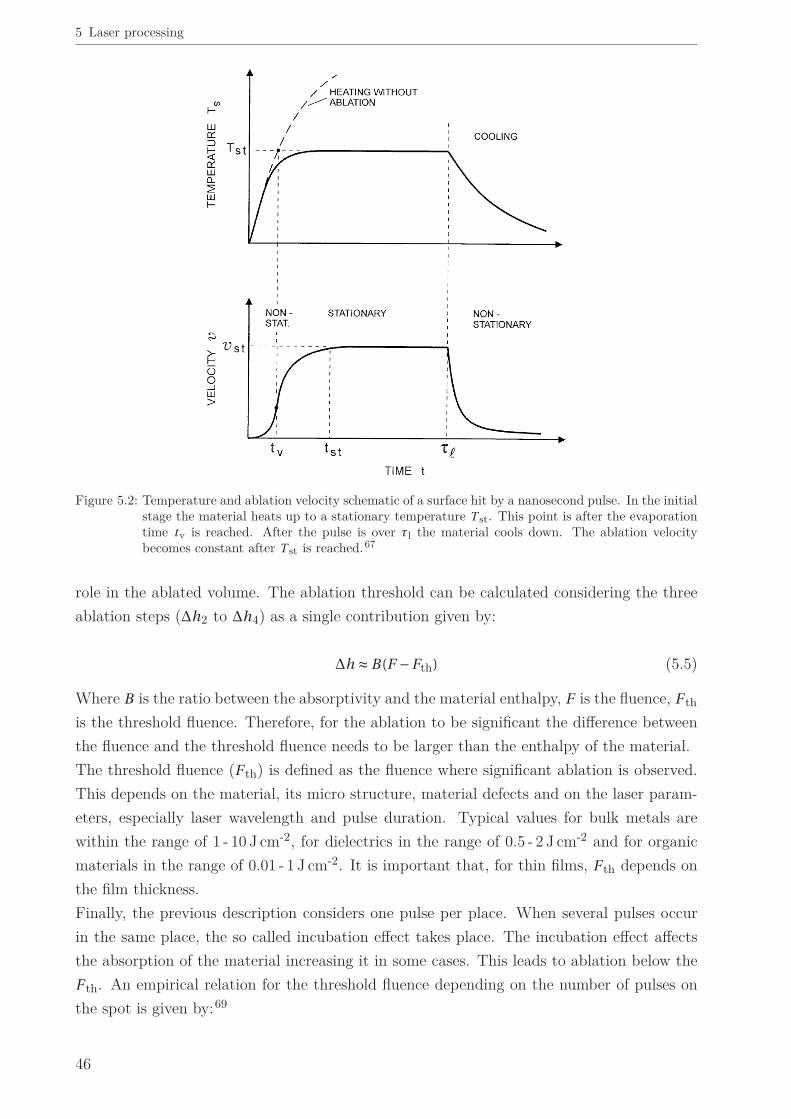
5 Laser processing
Figure 5.2: Temperature and ablation velocity schematic of a surface hit by a nanosecond pulse. In the initialstage the material heats up to a stationary temperature T st. This point is after the evaporationtime tv is reached. After the pulse is over τl the material cools down. The ablation velocitybecomes constant after T st is reached.67
role in the ablated volume. The ablation threshold can be calculated considering the threeablation steps (∆h2 to ∆h4) as a single contribution given by:
∆h ≈ B(F −Fth) (5.5)
Where B is the ratio between the absorptivity and the material enthalpy, F is the fluence, F th
is the threshold fluence. Therefore, for the ablation to be significant the difference betweenthe fluence and the threshold fluence needs to be larger than the enthalpy of the material.The threshold fluence (F th) is defined as the fluence where significant ablation is observed.This depends on the material, its micro structure, material defects and on the laser param-eters, especially laser wavelength and pulse duration. Typical values for bulk metals arewithin the range of 1 - 10 J cm-2, for dielectrics in the range of 0.5 - 2 J cm-2 and for organicmaterials in the range of 0.01 - 1 J cm-2. It is important that, for thin films, F th depends onthe film thickness.Finally, the previous description considers one pulse per place. When several pulses occurin the same place, the so called incubation effect takes place. The incubation effect affectsthe absorption of the material increasing it in some cases. This leads to ablation below theF th. An empirical relation for the threshold fluence depending on the number of pulses onthe spot is given by:69
46

5.3 Ultrashort pulsed laser ablation
Fthe(N ) = F1N S−1 (5.6)
Where F 1 is the single pulse threshold fluence, N is the number of pulses and S is theincubation coefficient. Therefore, it is expected that with a larger number of pulses in thesame location, the fluence necessary to ablate will decrease. The incubation effect is due toincrease of the absorption of the material. The absorption increase may be due to surfacemodifications.Although, nanosecond ablation offers unique advantages, for certain materials the pulses aretoo long for high quality structuring, specially for materials with high thermal conductivity.Therefore, pico and femtosecond laser ablation are feasible options that will be discussed inthe following section.
5.3 Ultrashort pulsed laser ablationUltrashort pulse laser ablation offers the advantage over nanosecond ablation of lower heataffected zones (HAZ) and higher precision structuring. It is mentioned in section 5.1 thatthe relaxation time between the electron and the lattice is between 10-12 to 10-10 s. If amaterial is ablated with a pulse which has a duration of 100 fs all the interactions within thematerial are electronic as there is not enough time for transmission of the energy from theelectrons to the lattice. Figure 5.3 depicts the different interaction times for femtosecondlaser interaction in metals and dielectrics.70
The higher structuring precision originates from the gaussian shape of the pulse. At lowerfluences closer to the threshold fluence, just the highest energy part of the pulse removesthe material. This allows high structuring precision, smaller than the spot size of the laserbeam.
Figure 5.3: Interaction times of femtosecond pulses with dielectric and metals.70
47
5 Laser processing
5.3.1 Ablation mechanisms in dielectrics and metals
The ablation process using ultrashort pulses is different for dielectrics and metals. Fordielectrics the initial step is to generate free electrons. The number of free electrons generatedin the material is defined by:
δntotalδt
= nmpi(I )+β(I )n (5.7)
where nmpi is the generation of free electrons due to multiphoton absorption and β(I ) is anintensity dependent impact ionization rate. Multiphoton absorption is strongly dependenton the laser intensity. For a pulse duration of 100 fs multiphoton ionization is the dominantabsorption mechanism for laser intensities higher than 1014 W cm-2.71 Once the energy isabsorbed and the free electrons are generated, the electron to electron collisions is multipliedby the inverse Bremsstrahlung (avalanche ionization). During this process electrons areaccelerated by the energy provided from the laser beam. The free electrons increase thelaser absorption leading to a higher number of free electrons. Due to the high density offree electrons the dielectric starts to behave as a metal. Afterward, the electrons leave thematerial, leaving a high concentration of positive ions on the surface. This positive ions thenare removed in the so called Coulomb explosion. The Coulomb explosion is a non-thermalprocess. After the pulse passes, the electrons transmit the remaining energy to the latticeand thermalization occurs.70
For metals the case is different as the electrons are already free. The electrons that absorbthe light take up energy. This leads to electron - electron thermalization, a process thattakes place in tens of fs. The diffusive energy transport by the high energy electrons willtake place as long as there is no thermal equilibrium between the electrons and the lattice.The thermal diffusion length that comes with this energy transfer is the key parameter forfs laser ablation.As the temperatures of the electrons and the lattice differs for both dielectrics and metals, thesurface temperature cannot be described using the classic heat equation (Equation 5.3).70
Instead two coupled differential equations are then needed:
Ce∂Te∂t
=∇· (ke∇Te)−Γ(Te−Tl)+Q
Cl∂Tl∂t
=∇· (kl∇Tl)−Γ(Te−Tl)(5.8)
Where T e and T l are the electron and lattice temperature, C e and C l are the heat capacitiesof the electron and the lattice and ke and k l are the electron and lattice heat conductivities.The Term Γ accounts for the coupling between the two equations. Q is the laser source that,in most cases, is assumed to have a Gaussian profile.
48

5.4 Threshold fluence determination and pulse overlap
5.3.2 Theoretical threshold fluence determination
Gamaly et al. developed a model to estimate the threshold fluence for dielectrics and met-als.71 The model starts using equation 5.7, evaluating the possibilities of having impactionization or multiphoton absorption. The final result for dielectrics is given by:
F dth = 3
16(εb+ Ji)
λneπ
(5.9)
and for metals:F m
th = 3
16(εb+εesc)
λneπ
(5.10)
where εb is the ion binding energy, J i is the ionization potential and εesc is the work function ofthe material. According to equation 5.9 the laser needs to overcome the ionization potentialto create free electrons plus the binding energy of the ions, resulting in material ablation.For the metals (equation 5.10), the ionization potential and the ion binding energy need tobe overcome. A linear relationship with the wavelength (λ) is also observed.
5.4 Threshold fluence determination and pulse overlapAs discussed above, the threshold fluence is the fluence where significant ablation is observed.Therefore, it is important to find an accurate method for its determination. Liu found alogarithmic relationship between the squared diameters of the single ablation spots and thethreshold fluence.72 This method has been further explained in different sources.73 37. Therelationship found by Liu is given by:
D2 = 2W 20 ln(
F
Fth) (5.11)
Where W 0 is the beam radius at the laser spot, D is the spot diameter. Due to the diffi-culties to measure W 0 accurately, the fluence is substituted by the pulse energy using therelationship:
F = Epulse
πW 20
(5.12)
where Epulse is the pulse energy E . Leading to the equation below;
D2 = 2W 20 ln(
E
Eth) (5.13)
Then the different squared diameters are plotted against the pulsed energies. In a graphicalrepresentation, a logarithmic scale is used on the x-axis, leading to a linear relationship.From the slope of the graph, W 0 is determined. Similarly, from the equation obtained fromthe linearization the threshold pulse energy (E th) is calculated. Finally, using equation 5.12,the threshold fluence is calculated.
49

5 Laser processing
A laser written line is constructed by overlapping the pulses. The pulse overlap is optimizedby testing different ablation speeds. The pulse overlap is given by:
Pulse overlap= 1− V
2W0 f(5.14)
Where f is the frequency of the laser and V is the structuring speed. The pulse overlapis important as a too high pulse overlap can lead to damage of the materials below. Aninsufficient pulse overlap may lead to incomplete electrical insulation and shorted electrodes,or poor contact between the electrodes in the case of a monolithic connection.
50

6 Femtosecond laser structuring of ITOon PET
Indium tin oxide (ITO) is a transparent conducting oxide that is commonly used in OPVand OLEDs. It has a high transmission of 90 % in the visible spectral regime and asheet resistance R = 12Ω-1 on glass and transmission of 80 % with a sheet resistanceR = 60Ω-1 on PET. To be used as an electrode in organic electronics, the ITO layerneeds to be structured. Methods to pattern the ITO often involve chemical etching or photo-lithography which offer high quality but are not compatible with roll-to-roll production.74,75
Ultrashort pulsed laser ablation is a proven technique to structure ITO on glass, producinghigh quality ablation with low bulges and electrical isolation of the different parts.76–78 Simi-larly, ultrashort pulsed laser ablation has been used to structure ITO on PET.79–82 However,the structuring of ITO on PET produced undesirable high bulges. The bulges may lead toshunts and defects in the devices as the layers on top are not thick enough to cover thebulges due to the thin-film nature of the devices. Hördemann introduced a method to re-duce the height of the bulges by using a sacrificial layer reducing the bulge height to lessthan 50 nm.83 The bulge height was also reduced using 5 passes with PO = 70% to less than100 nm. Other ideas were tested like using different beam shape like Top-Hat or Donut, butbulges higher than 100 nm were still produced. In this chapter, the ablation of ITO on PET(T500 nm = 80%, R = 60Ω-1, thickness = 90 nm, Sigma Aldrich) was explored. First thethreshold fluences ITO and PET were calculated for different wavelengths. The results arecompared to the respective absorption spectrum (section 6.1). The ITO structuring processwas then optimized for different wavelengths (section 6.2). Finally, section 6.3 concludesthis chapter.
6.1 Threshold fluence characterizationThe threshold fluences, for both ITO and PET, were determined using the Liu-method de-scribed in section 5.4 for eight different wavelengths λ= 360 nm, λ= 410 nm, λ= 450 nm,λ= 500 nm, λ= 550 nm, λ= 600 nm, λ= 650 nm and λ= 700 nm. Direct ablation was per-formed on the ITO side. The calculated focused waists were W 0 = 6.4 µm at λ= 360 nmand W 0 = 3.8 µm at λ= 700 nm. The difference is due to the different numerical aperturesof both objectives. Single pulse ablation was achieved by scribing lines using a speed of
51

6 Femtosecond laser structuring of ITO on PET
Figure 6.1: Threshold fluences at different wavelengths and absorption spectrum of ITO and PET. Thethreshold fluence shows no change for the ITO between λ= 410 nm and λ= 700 nm, however forPET it shows an increasing value with increasing wavelength. The maximum working windowfor selective ablation, marked in red, is given at λ= 700 nm.
180 mm s−1. The measured threshold fluences and the absorption spectrum, for both ITOand PET, are depicted in figure 6.1.A relationship between the absorption spectrum of ITO and its threshold fluences can beobserved. At λ= 360 nm, the absorption increases to 30%, translating in a reduction ofthe threshold fluence from F th = 170 mJ cm-2 to F th = 40 mJ cm-2. Between λ= 410 nm andλ= 700 nm, the threshold fluence of ITO remains constant at F th = 170 mJ cm−2 matchingthe absorption spectrum that remains constant with almost no absorption. The thresholdfluence is different to the F th = 250 mJ cm−2 reported by McDonell et al. for λ= 343 nm atλ= 1030 nm.80 The difference can be explained by the different pulse length used in bothstudies, 90 fs compared to 500 fs.The threshold fluence for PET does not follow the absorption spectrum as it shows anincreasing magnitude towards higher wavelengths while the absorption strength remainsconstant. This matches equation 5.9 where a linear dependency of the threshold fluence onthe wavelength is described. The equation does not describe the threshold fluences of ITO.One possible explanation is that the equation was developed to describe bulk materials suchas the PET substrate rather than transparent thin-films such as ITO.Finally, the best wavelength to achieve selective ablation is at λ= 700 nm where the work-ing window is the largest. The working window is the difference between the thresholdfluence of ITO and PET. This is marked in red in figure 6.1. In contrast, selective ab-lation at λ= 360 nm is complicated as both materials have a similar threshold fluence,F th = 40 mJ cm-2.
52
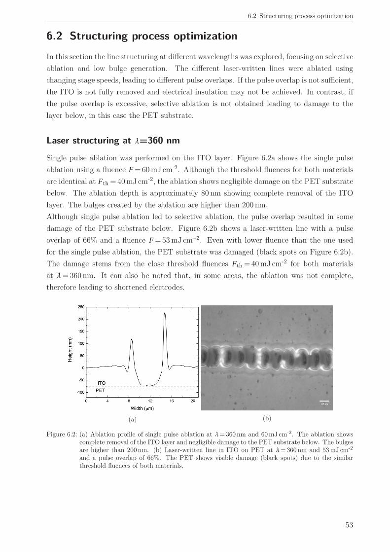
6.2 Structuring process optimization
6.2 Structuring process optimizationIn this section the line structuring at different wavelengths was explored, focusing on selectiveablation and low bulge generation. The different laser-written lines were ablated usingchanging stage speeds, leading to different pulse overlaps. If the pulse overlap is not sufficient,the ITO is not fully removed and electrical insulation may not be achieved. In contrast, ifthe pulse overlap is excessive, selective ablation is not obtained leading to damage to thelayer below, in this case the PET substrate.
Laser structuring at λ=360 nm
Single pulse ablation was performed on the ITO layer. Figure 6.2a shows the single pulseablation using a fluence F = 60 mJ cm-2. Although the threshold fluences for both materialsare identical at F th = 40 mJ cm-2, the ablation shows negligible damage on the PET substratebelow. The ablation depth is approximately 80 nm showing complete removal of the ITOlayer. The bulges created by the ablation are higher than 200 nm.Although single pulse ablation led to selective ablation, the pulse overlap resulted in somedamage of the PET substrate below. Figure 6.2b shows a laser-written line with a pulseoverlap of 66% and a fluence F = 53 mJ cm−2. Even with lower fluence than the one usedfor the single pulse ablation, the PET substrate was damaged (black spots on Figure 6.2b).The damage stems from the close threshold fluences F th = 40 mJ cm-2 for both materialsat λ= 360 nm. It can also be noted that, in some areas, the ablation was not complete,therefore leading to shortened electrodes.
(a) (b)
Figure 6.2: (a) Ablation profile of single pulse ablation at λ= 360 nm and 60 mJ cm-2. The ablation showscomplete removal of the ITO layer and negligible damage to the PET substrate below. The bulgesare higher than 200 nm. (b) Laser-written line in ITO on PET at λ= 360 nm and 53 mJ cm-2
and a pulse overlap of 66%. The PET shows visible damage (black spots) due to the similarthreshold fluences of both materials.
53

6 Femtosecond laser structuring of ITO on PET
Laser structuring at λ=410 nm
Laser structuring was performed at λ= 410 nm. A fluence F = 200 mJ cm-2 was tested. Thisfluence is slightly higher than the threshold fluence F th = 170 mJ cm-2 of ITO but lower thanthe one of PET, F th = 240 mJ cm-2, at the given wavelength. Figure 6.3a shows a confocal 3Dimage of a laser-written line with a pulse overlap of 69%. Selective ablation was performedwith no visible damage to the PET substrate below. However, the height of the bulges is≥ 250 nm. This is confirmed on the profile image of the selected line (Figure 6.3b). The highbulges may lead to shorts with the top electrode. The laser-written line width is < 5 µm.The pulse overlap was increased to 85%, to evaluate the effect on the bulges keeping thefluence constant at F = 200 mJ cm-2. Figure 6.3c shows a confocal 3D image of the resultinglaser-written line. The highest bulge is around 100 nm showing a significant improvementwhen compared to the lower pulse overlap. However, the higher pulse overlap led to damageof the PET substrate below as shown by the dark spots that go below 250 nm.
(a) (b)
(c) (d)
Figure 6.3: Comparison between laser-written lines at λ= 410 nm with different pulse overlaps. (a) and (b)show the 3D image and confocal profile of a laser-written line with a pulse overlap of 69%. Thelaser-written line shows selective ablation with negligible damage to the PET substrate below.However, the bulges are higher than 200 nm as shown in the profile picture (b). (c) and (d) showthe 3D image and confocal profile when the pulse overlap is increased to 85%. The bulges improvearound 100 nm (confocal profile (d)). However, the substrate shows damage due to the higherpulsed overlap. Both lines were structured with a F = 200 mJ cm-2 and have a laser-written linewidth of ≤5 µm.
54

6.2 Structuring process optimization
There is no significant increase on the laser-written line width as it remained ≤ 5 µm (Figure6.3d). The damage may be created due to an incubation effect created by the higher pulseoverlap. The incubation effect enhances the absorption of the PET.
Laser structuring at λ=550 nm
Due to the increment on the PET threshold fluence to F th = 427 mJ cm-2, the working win-dow becomes larger at λ= 550 nm than at λ= 410 nm. Hence a higher fluence was chosenF = 280 mJ cm-2 to evaluate the laser-written lines at λ= 550 nm. Using a pulse overlap of72%, selective ablation was achieved, however, the observed bulges were higher than 200 nm.Following the observations at λ= 410 nm where the increase in pulse overlap led to lowerbulges, the pulse overlap was increased to 89% at λ= 550 nm. The laser-written lines exhibitselective ablation, with negligible damage to the PET substrate. The bulges are reduced toapproximately 100 nm. The width of the laser-written lines is < 5 µm (Figure 6.4).
(a) (b)
(c) (d)
Figure 6.4: Comparison between laser-written lines at λ= 550 nm with different pulse overlaps. (a) and (b)show the 3D image and confocal profile of a laser-writtend line with a pulse overlap of 89%. Thelaser-written line shows selective ablation with negligible damage to the PET substrate below.The bulges are around 100 nm as shown in the profile picture (b). (c) and (d) show the 3D imageand confocal profile when the pulse overlap is increased to 95%. The bulges improve to ≤ 50 nm(confocal profile (d)). Selective ablation is achieved with negligible damage to the PET substratebelow. Both lines were structured with a F = 280 mJ cm-2 and have a laser-written line width of≤5 µm.
55

6 Femtosecond laser structuring of ITO on PET
Similar to the case with λ= 410 nm, a higher pulse overlap of 95% for λ= 550 nm wasevaluated, keeping the fluence constant at F = 280 mJ cm-2. Figure 6.4c depicts selectiveablation with negligible damage to the PET substrate. The bulge height is further decreasedto ≤ 50 nm. The largest operating window at λ= 550 nm provides the opportunity to increasethe pulse overlap to 95% without damaging the PET substrate below. The confocal profileimage (Figure 6.4d) of the ablation confirms the negligible damage to the PET substrate.The width of the laser-written lines is < 5 µm.
Laser structuring at λ=650 nm
At λ= 650 nm, the working window is similar to the one at λ= 550 nm as the thresholdfluence of λ= 650 nm of PET is F th = 430 mJ cm-2. A lower fluence F = 240 mJ cm-2 wasevaluated. Figure 6.5a shows a confocal 3D image of a laser-written line using a pulseoverlap of 90 %.
(a) (b)
(c) (d)
Figure 6.5: Comparison between laser-written lines at λ= 650 nm with different pulse overlaps. (a) and (b)show the 3D image and confocal profile of a laser-written line with a pulse overlap of 90%. Thelaser-written line shows selective ablation with little damage to the PET substrate below. Thebulges are around 50 nm as shown in the profile picture (b).(c) and (d) show the 3D image andconfocal profile when the pulse overlap is increased to 95%. The bulges remain consistent around50 nm (confocal profile (d)). Slight damage, in the order of 20 nm, is visible. Both lines werestructured with a F = 240 mJ cm-2 and have a laser-written line width of ≤5 µm.
56
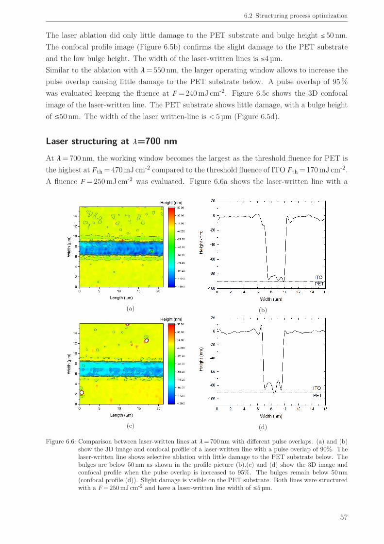
6.2 Structuring process optimization
The laser ablation did only little damage to the PET substrate and bulge height ≤ 50 nm.The confocal profile image (Figure 6.5b) confirms the slight damage to the PET substrateand the low bulge height. The width of the laser-written lines is ≤4 µm.Similar to the ablation with λ= 550 nm, the larger operating window allows to increase thepulse overlap causing little damage to the PET substrate below. A pulse overlap of 95 %was evaluated keeping the fluence at F = 240 mJ cm-2. Figure 6.5c shows the 3D confocalimage of the laser-written line. The PET substrate shows little damage, with a bulge heightof ≤50 nm. The width of the laser written-line is < 5 µm (Figure 6.5d).
Laser structuring at λ=700 nm
At λ= 700 nm, the working window becomes the largest as the threshold fluence for PET isthe highest at F th = 470 mJ cm-2 compared to the threshold fluence of ITO F th = 170 mJ cm-2.A fluence F = 250 mJ cm-2 was evaluated. Figure 6.6a shows the laser-written line with a
(a) (b)
(c) (d)
Figure 6.6: Comparison between laser-written lines at λ= 700 nm with different pulse overlaps. (a) and (b)show the 3D image and confocal profile of a laser-written line with a pulse overlap of 90%. Thelaser-written line shows selective ablation with little damage to the PET substrate below. Thebulges are below 50 nm as shown in the profile picture (b).(c) and (d) show the 3D image andconfocal profile when the pulse overlap is increased to 95%. The bulges remain below 50 nm(confocal profile (d)). Slight damage is visible on the PET substrate. Both lines were structuredwith a F = 250 mJ cm-2 and have a laser-written line width of ≤5 µm.
57
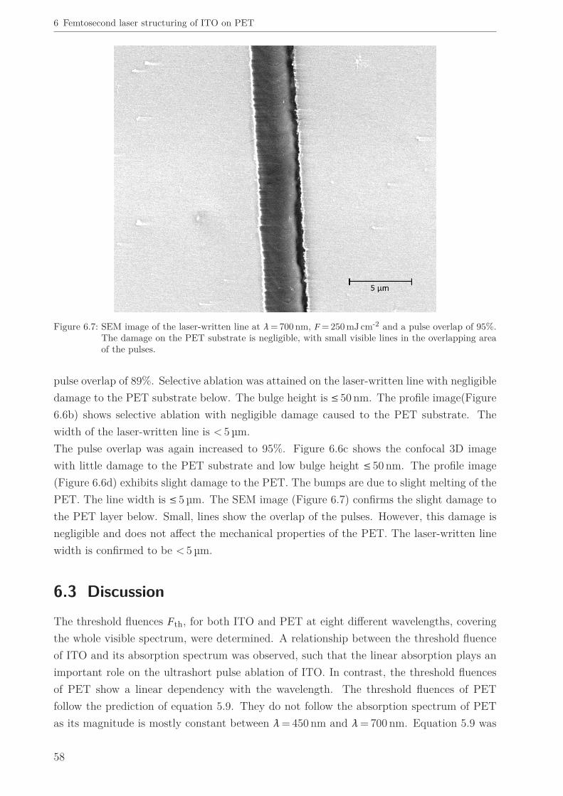
6 Femtosecond laser structuring of ITO on PET
Figure 6.7: SEM image of the laser-written line at λ= 700 nm, F = 250 mJ cm-2 and a pulse overlap of 95%.The damage on the PET substrate is negligible, with small visible lines in the overlapping areaof the pulses.
pulse overlap of 89%. Selective ablation was attained on the laser-written line with negligibledamage to the PET substrate below. The bulge height is ≤ 50 nm. The profile image(Figure6.6b) shows selective ablation with negligible damage caused to the PET substrate. Thewidth of the laser-written line is < 5 µm.The pulse overlap was again increased to 95%. Figure 6.6c shows the confocal 3D imagewith little damage to the PET substrate and low bulge height ≤ 50 nm. The profile image(Figure 6.6d) exhibits slight damage to the PET. The bumps are due to slight melting of thePET. The line width is ≤ 5 µm. The SEM image (Figure 6.7) confirms the slight damage tothe PET layer below. Small, lines show the overlap of the pulses. However, this damage isnegligible and does not affect the mechanical properties of the PET. The laser-written linewidth is confirmed to be < 5 µm.
6.3 DiscussionThe threshold fluences F th, for both ITO and PET at eight different wavelengths, coveringthe whole visible spectrum, were determined. A relationship between the threshold fluenceof ITO and its absorption spectrum was observed, such that the linear absorption plays animportant role on the ultrashort pulse ablation of ITO. In contrast, the threshold fluencesof PET show a linear dependency with the wavelength. The threshold fluences of PETfollow the prediction of equation 5.9. They do not follow the absorption spectrum of PETas its magnitude is mostly constant between λ= 450 nm and λ= 700 nm. Equation 5.9 was
58

6.3 Discussion
determined using the assumption of a bulk material and surface processes on the skin layer.This results could help further theoretical work to explain the interaction of femtosecondlasers with thin films at different wavelengths.Here, femtosecond laser structuring allowed to selectively structure ITO on top of PETwith low bulges ≤ 50 nm and slight damage to the ITO substrate below at three differentwavelengths λ= 550 nm, λ= 650 nm and λ= 700 nm. At λ= 410 nm, selective ablation wasachieved, however high bulges ≥ 200 nm were still produced. In all the evaluated wavelengths,the bulge height decreased with higher pulse overlaps. Therefore, a large working windowis important as it allows a higher pulse overlap without damaging the layer below as it wasdemonstrated in this work. The laser-written line widths were in all cases < 5 µm. The linewidth is below the waist W 0 of the objectives. This demonstrate that femtosecond laser cansuccessfully achieved high precision under the waist of the focused beam. The small linewidth will lead to smaller inactive areas on monolithically connected devices like OLEDsor OPVs modules. The best results were demonstrated at λ= 700 nm, F = 250 mJ cm-2 andpulse overlap of 95%. The low bulges will allow the construction of thin-film devices on topof the ITO layer without shunts that decrease their performance. The selective ablation willallow the use of PET substrates for applications that require mechanical flexibility.
59

7 OLED modules structured byfemtosecond laser ablation
OLEDs are rapidly becoming a new tendency on displays and luminaries. Several companiesuse them on mobile phones and flat screen TVs. For illumination large display areas arerequired. However, large areas come with detriment of the light homogeneity due to voltagelosses.42 The voltage losses are caused by the high sheet resistance of the transparent elec-trodes, typically ITO. The problem increases when the OLED area increases as the drivingcurrent of the OLED depends on the size of the device. The most common concept to solvethis issue is to use of metal bus bars that improve the conductivity.44,45,84–86 However, thebus bars are visible reducing its appeal. The bus bars have a typical height of 300 - 500 nm,which exceeds the common thickness of the light emitting layers, that is, ≤100 nm. Thiscan lead to shorts, and passivisation layers are necessary to solve this problem. A differentapproach is to monolithically connect the OLEDs into a large-scale module. The operatingcurrent then is limited by the smaller area of each individual OLED. This concept has beenproven by Dugal et al.52
In this chapter, femtosecond laser structured OLED modules are described. In section 7.1the used materials, the architecture and the device design of the OLED module are described.In section 7.2 the threshold fluences were calculated for 5 different wavelengths λ= 550 nm,λ= 600 nm, λ= 650 nm, λ= 700 nm and λ= 750 nm. Section 7.3 presents the optimizedprocess to structure process P1, P2 and P3 for two different wavelengths λ= 550 nm andλ= 700 nm. Section 7.4 describes the optoelectronic characterization of the devices. Section7.5 gives our conclusions. Parts of this section are reprinted and adapted from Fragoso etal.87
7.1 Materials, device design and architecture
7.1.1 Materials
The materials used for the OLEDs need to comply with several specifications. Besides theelectronic requirements necessary to bring the free carriers into the device, the processibilityof the materials is crucial to fabricate the devices. For the electron injection layer (EIL) andthe emitting layer the feasibility to process the material from solution is necessary. For thehole injection layer (HIL) and the metal electrodes vacuum evaporation of the materials isrequired.
61

7 OLED modules structured by femtosecond laser ablation
Zinc oxide
Zinc oxide (ZnO) is a transition metal oxide that has high electron mobility, wide bandgap (3.3 eV) and low work function (4.2 eV).88 Due to its electronic properties, it is usedas electron injection and transport layer. It is also a material with low reactivity, leadingto better stability on the devices.88,89 In this experiments the layers were produced froma nanoparticle dispersion (N10, Avantama Ag. 0.55 wt% in isopropanol). After depositionof the layers the samples were annealed under nitrogen atmosphere on a hotplate (150°,10 min).90
Polyethylenimine (PEI)
PEI is used to modify the work function of ZnO and facilitate the injection of electrons.91 Anultrathin layer (1 to 10 nm) is applied on top of the ZnO layer. The work function is modifieddue to the ethylamine dipole within the self assembled monolayer (SAM) and the dipolebetween the SAM and the ZnO layer. The PEI layer is spincoated from a 2-methoxyethanolsolution (0.4 wt%). After the application the samples were washed in ethanol and annealedunder ambient atmosphere on a hotplate (100°C, 10 min). The work function of the bilayer(ZnO/PEI) is 3.3 eV.90
SuperYellow
SuperYellow is a yellow emitting polymer (Merck KGaA). The color of the emitted lightin CIE 1931 XYZ color space is shown in Figure 7.1a.92 SuperYellow has a HOMO level of-5.4 eV and LUMO level of -3.0 eV, resulting in a band gap of 2.4 eV. The molecular structureof SuperYellow is shown in figure 7.1b.
(a) (b)
Figure 7.1: (a) SuperYellow emission in the CIE 1931 XYZ color space. (b) Molecular structure of SuperYel-low.92
62

7.2 Threshold fluence characterization
Molybdenum trioxide (MoO3)
Molybdenum trioxide was used as HIL. A 10 nm layer was evaporated in high vacuum forthis work. The work function of the MoO3 layer is -5.9 eV. MoO3 has been previously usedin OLEDs leading to stable devices as the HIL encapsulates the emitting layer.93.
7.1.2 Architecture and sample design
Figure 7.2a depicts the architecture and layer thicknesses of the OLED modules. ITO isused as bottom electrode. ZnO/PEI is the electron injection layer and SuperYellow is theemitting layer. MoO3 is the hole injection layer and silver is the top electrode.The individual OLEDs are connected in a module by structuring ITO as P1 to electricallyisolate the bottom electrode. ZnO/PEI/SuperYellow is structured as P2 to permit theelectrical connection between the OLEDs. MoO3 and silver are structured as P3 to separatethe top electrode.The OLED module was designed on a 25 x 25 mm2 ITO coated glass substrate (Figure 7.2b).The design permits the measurement of the individual OLEDs when two OLEDs per sub-strate are built. The total emitting area of the device is 1.625 cm2. The ITO contact waslaser structured twice, once for the P1 structuring step of the monolithic connection andonce to isolate the top contact from the bottom electrode of the OLED B. The silver/MoO3
top electrode was evaporated through a mask. The P3 step of the monolithic connectionwas structured using the laser on the silver.
7.2 Threshold fluence characterizationThe threshold fluences were determined for five different wavelengths from λ= 550 nm toλ= 750 nm with 50 nm steps using the Liu method described in section 5.4. This rangeincludes the wavelengths of the Ti:Sapphire laser and several commonly used green lasers.The ablation tests were done on proxy devices using the device architecture (figure 7.2a)
(a) (b)
Figure 7.2: (a) OLED module architecture showing the P1, P2, P3 steps for the monolithic connection. (b)Sample design on a 25 x 25 mm2 ITO coated glass substrate. The total emitting area of the deviceis 1.625 cm2.
63

7 OLED modules structured by femtosecond laser ablation
to consider the influence of the layers underneath. Single spots were attained by mov-ing the µFAB stage at 180 mm s-1. The calculated focused waist was W 0 = 3.5 µm atλ= 750 nm.Figure 7.3a shows the threshold fluences for the three materials ablated in steps P1, P2and P3. The threshold of ITO ,F th = 170 mJ cm-2, remains consistent during the wholewavelength range. SuperYellow threshold fluences, F th = 40 mJ cm-2, also remain constantfor all wavelengths. A similar tendency of the threshold fluences and the absorption isobserved for both materials (figure 7.3b). The absorption spectra have a slight increase inabsorption, however this is not significant and it is not reflected in the threshold fluences.The threshold fluences at different wavelengths do not follow equation 5.9 that expects alinear increase of the ablation threshold with the wavelength. It is possible that the differencestems from the thin-film nature of the layers.Different to what was observed for ITO and ZnO/PEI/SuperYellow, the threshold fluencefor MoO3/Silver (P3) increases linearly with the wavelength, from F th = 230 mJ cm-2 atλ= 550 nm to F th = 490 mJ cm-2 at λ= 750 nm (Figure 7.3a). The decrease in absorptionbetween λ= 550 nm and λ= 750 nm could partially explain the increase of the thresholdfluence. However, this tendency follows equation 5.10 where a linear relationship betweenthe wavelength and the threshold fluence is established. Although the MoO3/Silver layer isalso a thin-film, it is not semitransparent like ITO and ZnO/PEI/SuperYellow. This mayexplain the different tendencies for MoO3/Silver, and ITO and ZnO/PEI/SuperYellow.To facilitate the selective ablation of one layer on top of another it is important to havea working window, defined by the difference of the threshold fluences. Figure 7.3a clearlyshows that for the selective ablation of ZnO/PEI/SuperYellow (P2) on top of ITO there isan equal working window for all the studied wavelengths. For the ablation of MoO3/Silver(P3), the required fluence to structure P3 is higher than the one necessary to structure P1
(a)(b)
Figure 7.3: (a) Threshold fluence for ITO (P1), ZnO/PEI/SuperYellow (P2) and MoO3 for five differentwavelengths (b) absorption spectra for ITO (P1), ZnO/PEI/SuperYellow (P2) and MoO3/silver(P3).
64

7.3 Structuring process optimization
and P2. Therefore, the optimization of the pulse overlap is crucial to structure MoO3/Silver(P3).
7.3 Structuring process optimizationIn this section, line structuring with different wavelengths is explored. The lines are writtenby overlapping the pulses. The conditions are adjusted by changing the speed of the XYZstage. An insufficient pulse overlap might lead to incomplete ablation, hence creating shortsor a high sheet resistance. An excessive ablation may lead to the damage of the layerbelow. The structuring requirements change depending on the ablation step. For ITO (P1),consistent lines are required (to achieve electrical insulation), with low bulges and smalldamage to the glass substrate below. For ZnO/PEI/SuperYellow (P2) selective ablationwith a clean removal of the materials is the most important. Damage of the ITO belowwould hamper the performance or even prevent the operation of the device. If parts ofthe layers are not ablated, the series resistance of the device may increase, leading to lowerefficiencies. Finally in the case of MoO3/Silver (P3), it is most important not to damagethe ITO layer below. The ZnO/PEI/SuperYello below can be damaged without affectingthe device performance, however it is desirable to keep it as it functions as a buffer layerin case of melting of the silver top electrode during the ablation process. The melted silvermay lead to shorts if it contacts the bottom electrode.There is a constant working window for the structuring of P2 for all five studied wavelengths.The structuring processes were optimized for the two extreme cases, at λ= 550 nm and atλ= 750 nm.
7.3.1 ITO structuring (P1)
Several fluences above the threshold fluence were tested to structure ITO (P1). The optimumparameters were F = 370 mJ cm-2, pulse overlap of 86 % at λ1 = 550 nm and F = 350 mJ cm-2,
Figure 7.4: ITO structuring (P1) at λ= 550 nm and λ= 750 nm. Slight damage to the glass substrate belowis observed. The bulge is low, in the order of 20 nm, and the structured line width is ≤10 µm forboth wavelenghts.
65

7 OLED modules structured by femtosecond laser ablation
pulse overlap of 73 % at λ2 = 750 nm. Both processes led to clean ablation with slight damageto the glass substrate below and electrical insulation. The slight damage on the glass sub-strate does not hamper the device performance. The bulge is low in the order of 20 nm andthe line width is < 10 µm allowing small inactive areas. The ablation processes at both wave-lengths led to electrical insulation. Figure 7.4 depicts the confocal profile for the ablationprocesses at both wavelengths.
7.3.2 ZnO/PEI/SuperYellow structuring (P2)
Several fluences within the operating window were tested to structure ZnO/PEI/SuperYellow(P2). The optimum parameters were F = 110 mJ cm-2, pulse overlap of 85 % at λ1 = 550 nmand F = 240 mJ cm-2, pulse overlap of 86 % at λ2 = 750 nm. Similar to the case for the ITO,the laser-written lines have a width of < 10 µm. The structuring process at λ2 = 750 nmrequires a higher fluence to fully remove the ZnO layer below and to allow a direct connectionbetween the silver and the ITO. Figure 7.5a shows the confocal profile pictures of the laser-written lines, where nice selective ablation is achieved as no visible damage to the ITOlayer is shown. This is further confirmed in figure 7.5b where the SEM picture shows themonolithic connection between the silver and the ITO layers with negligible damage to theITO layer. The bulges are higher than 80 nm, however, they do not play a significant roleon the P2 ablation. In both cases, the relative high pulse overlap is necessary to remove theZnO layer without any residues and to allow a good connection between the ITO and thesilver layers.
(a) (b)
Figure 7.5: (a) Confocal profile image of the laser-written lines of the ZnO/PEI/SuperYellow (P2) usingλ= 550 nm and λ= 750 nm. Negligible damage to the ITO electrode below is visible. Bulges arepresent, however, they are not detrimental to the performance of the device. (b) SEM imageshowing the ablation of ZnO/PEI/SuperYellow (P2) at λ= 750 nm. The monolithic connection,between the silver and the ITO, is visible. The ITO shows negligible damage on the spot wherethe ablation took place.
66

7.4 Optoelectronic characterization
7.3.3 MoO3/silver (P3) structuring
Several fluences above the silver threshold fluence were tested to structure MoO3/silver(P3). The optimum parameters were F = 340 mJ cm-2, pulse overlap of 65% at λ1 = 550 nmand F = 540 mJ cm-2, pulse overlap of 66% at λ2 = 750 nm. The higher fluence used atλ2 = 750 nm reflects the higher threshold fluence. Figure 7.6a shows the confocal profileimage of the laser-written lines using both wavelengths. At λ1 = 550 nm, the ablation depth(140 nm) shows slight damage to the ZnO/PEI/SuperYellow layers underneath. However,this minor damage does not hamper the functionality of the device as the ITO is unscathed.Although a higher fluence was used at λ2 = 750 nm, similar results to the ones observed atλ1 = 550 nm are present, with slight damage to the ZnO/PEI/SuperYellow layers underneathand no visible damage to the ITO layer underneath. The bulges are higher than 200 nm,however, as there are no layers on top of P3, this does not affect the performance of thedevice. Figure 7.6b shows the SEM image of the P3 structured line at λ2 = 750 nm. Thelow contrast SuperYellow looks blacked. In the regions where the pulse overlapped, damageto the ZnO/PEI/SuperYellow is present. However, the image confirms that the ITO (false-colored) is intact. An increase on the pulse overlap to 89% leads to complete removal of theITO layer, hence preventing the operation of the devices.
7.4 Optoelectronic characterizationFollowing the optimization of the structuring processes for P1, P2 and P3, single OLEDs aswell as two and three OLED modules were built. Each OLED module has an active area of1.625 cm2. For the OLED modules, this area was divided in two or three parts. As depictedin figure 7.2a, the area defined by the width between P1 and P3 is inactive and hence notemissive. Figure 7.7a shows the confocal 3D profile image of a representative P1, P2 and P3
(a) (b)
Figure 7.6: (a) Confocal profile image of the laser-written lines of MoO3/silver (P3) at λ= 550 nm and atλ= 750 nm. Negligible damage to the ITO electrode below is visible. The ablation depth showsdamage to the ZnO/PEI/SuperYellow layers underneath. (b) SEM image showing the ablationof MoO3/silver (P3) at λ= 750 nm. The low contrast SuperYellow appears black on the image.The ZnO/PEI/SuperYellow is damaged where the pulses overlap. The ITO appears unscathed.
67
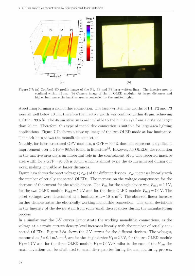
7 OLED modules structured by femtosecond laser ablation
(a) (b)
Figure 7.7: (a) Confocal 3D profile image of the P1, P3 and P3 laser-written lines. The inactive area isconfined within 45 µm. (b) Camera image of the lit OLED module. At larger distances andhigher luminance the inactive area is concealed by the emitted light.
structuring forming a monolithic connection. The laser-written line widths of P1, P2 and P3were all well below 10 µm, therefore the inactive width was confined within 45 µm, achievinga GFF = 99.6 %. The 45 µm structures are invisible to the human eye from a distance largerthan 20 cm. Therefore, this type of monolithic connection is suitable for large-area lightingapplications. Figure 7.7b shows a close up image of the two OLED mode at low luminance.The dark lines shows the monolithic connection.Notably, for laser structured OPV modules, a GFF = 99.6% does not represent a significantimprovement over a GFF = 98.5% found in literature94. However, for OLEDs, the reductionin the inactive area plays an important role in the concealment of it. The reported inactivearea width for a GFF = 98.5% is 80 µm which is almost twice the 45 µm achieved during ourwork, making it visible at larger distances.Figure 7.8a shows the onset voltages (V on) of the different devices. V on increases linearly withthe number of serially connected OLEDs. The increase on the voltage compensates for thedecrease of the current for the whole device. The V on for the single device was V on1 = 2.7 V,for the two OLED module V on2 = 5.2 V and for the three OLED module V on3 = 7.0 V. Theonset voltages were determined at a luminance L = 10 cd m-2. The observed linear increasefurther demonstrates the electrically working monolithic connection. The small deviationsin the linearity of the device stem from some small discrepancies during the manufacturingprocess.In a similar way the J-V curves demonstrate the working monolithic connections, as thevoltage at a certain current density level increases linearly with the number of serially con-nected OLEDs. Figure 7.8a shows the J-V curves for the different devices. The voltages,measured at J = 0.1 mA cm-2, are for the single device V 1 = 2.3 V, for the two OLED moduleV 2 = 4.7 V and for the three OLED module V 3 = 7.0 V. Similar to the case of the V on, thesmall deviations can be attributed to small discrepancies during the manufacturing process.
68
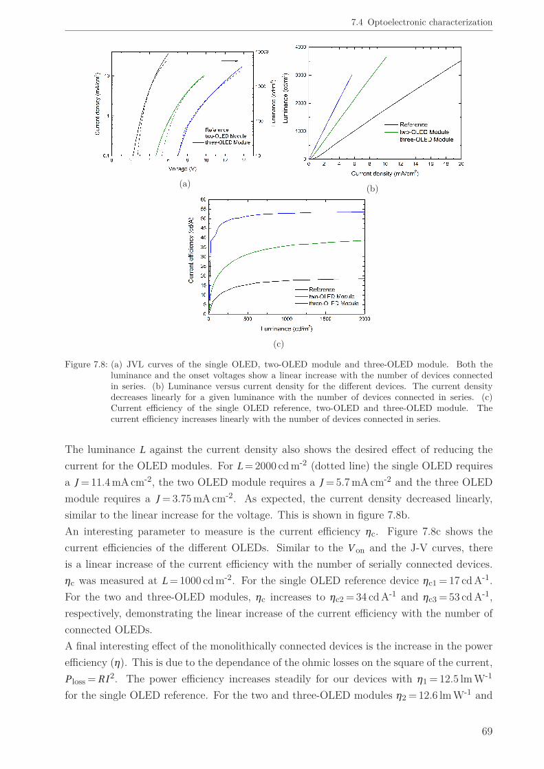
7.4 Optoelectronic characterization
(a) (b)
(c)
Figure 7.8: (a) JVL curves of the single OLED, two-OLED module and three-OLED module. Both theluminance and the onset voltages show a linear increase with the number of devices connectedin series. (b) Luminance versus current density for the different devices. The current densitydecreases linearly for a given luminance with the number of devices connected in series. (c)Current efficiency of the single OLED reference, two-OLED and three-OLED module. Thecurrent efficiency increases linearly with the number of devices connected in series.
The luminance L against the current density also shows the desired effect of reducing thecurrent for the OLED modules. For L = 2000 cd m-2 (dotted line) the single OLED requiresa J = 11.4 mA cm-2, the two OLED module requires a J = 5.7 mA cm-2 and the three OLEDmodule requires a J = 3.75 mA cm-2. As expected, the current density decreased linearly,similar to the linear increase for the voltage. This is shown in figure 7.8b.An interesting parameter to measure is the current efficiency ηc. Figure 7.8c shows thecurrent efficiencies of the different OLEDs. Similar to the V on and the J-V curves, thereis a linear increase of the current efficiency with the number of serially connected devices.ηc was measured at L = 1000 cd m-2. For the single OLED reference device ηc1 = 17 cd A-1.For the two and three-OLED modules, ηc increases to ηc2 = 34 cd A-1 and ηc3 = 53 cd A-1,respectively, demonstrating the linear increase of the current efficiency with the number ofconnected OLEDs.A final interesting effect of the monolithically connected devices is the increase in the powerefficiency (η). This is due to the dependance of the ohmic losses on the square of the current,P loss = RI 2. The power efficiency increases steadily for our devices with η1 = 12.5 lm W-1
for the single OLED reference. For the two and three-OLED modules η2 = 12.6 lm W-1 and
69
7 OLED modules structured by femtosecond laser ablation
Table 7.1: Key performance parameters for the different single two and three OLED modules.
Device V on (at 10 cd m-2) ηc (at 1000 cd m-2) η(at 1000 cd m-2)
Reference 2.7 V 17 cd A-1 12.5 lm W-1
Two-OLED module 5.3 V 34 cd A-1 12.6 lm W-1
Three-OLED module 7.0 V 53 cd A-1 14.0 lm W-1
η1 = 14.0 lm W-1 were achieved, again demonstrating the advantage of connecting the devicesin series. Table 7.1 shows the key performance parameters of the different devices.
7.5 DiscussionUltrashort pulsed laser structuring has been used to structure OLED modules. The studyof the threshold fluence dependency on the wavelength shows that, for the semitransparentthin-films, the threshold fluences do not follow the equation 5.9 where a linear relationshipbetween the threshold fluence and the wavelength is stated. However, this is not the casefor the silver top electrode that shows linear increase with higher wavelengths as describedin equation 5.10. This infers that, for thin semitransparent films, the linear absorption playa more important role than the non linear absorption. The results shown in this work couldhelp to further understand the femtosecond ablation process with different wavelengths forthin-films.It was demonstrated that it is feasible to structure P1, P2 and P3, for the described ar-chitecture (figure 7.2a), with both wavelengths λ= 550 nm and λ= 750 nm. It is importantto consider that selective ablation was achieved for the case of the silver, with damage onthe SuperYellow underneath just on the overlapped area. With a more stable laser, whereseveral non linear processes are not required to achieve the desired wavelength, it would bepossible to achieve selective ablation by controlling the overlap and reducing it to a mini-mum. The presence of SuperYellow reduces the possibility of shunts between the top silverelectrode and the bottom ITO electrode, reducing the number of failed devices. The possiblereduction of failed devices is a key point for any production on an industrial scale.The OLED modules show better optoelectronic characteristics than the single OLED refer-ence devices as reflected by higher currents and power efficiencies. It is important to makefurther studies on the number of devices that may be connected in series. These studieshave already been performed on OPV modules where a relationship between the number ofdevices, the width of the inactive area and the resistivity of the electrodes has been found.95
The monolithic connection was demonstrated to work based on the increase of the onsetvoltages with the number of devices connected in series. Importantly. the reduced widthof the inactive area that was achieved (≤45 µm) helps to conceal this non-emissive area andmakes the laser a suitable tool to process large-area OLEDs for lighting applications.A final interesting study to be performed in the future is the monolithic connection oftandem OLEDs. This would lead to further decrease of the current, leading to higher current
70

7.5 Discussion
efficiencies and more stable devices. The reduced current will also translate into a higherpower efficiency that is an important selling point for luminaires.Finally, it can be concluded that lasers are a suitable tool for industrial processes. In theablation processes discussed herein, just a minimal fraction of the laser power was used.Therefore, the splitting of the beam for parallel ablation of several lines is possible. Alsothe developments of new femtosecond lasers with repetition rates in the range of hundredsof KHz or even MHz will allow the fast processing in roll-to-roll devices with speeds as highas 1 m s-1.
71


8 Single-junction and tandem solarmodules on top of ITO
Organic solar cells have reached PCEs above 13 % in small-scale devices with photoactiveareas around 10 mm2.28 When the device is scaled up, the sheet resistance of the semi-transparent electrode, typically ITO, hampers the performance of the device. To reduce thiseffect the device is separated into several small units. The units are then connected inseries, effectively reducing the total current of the device and increasing the voltage. This isusually accomplished through a monolithic connection as explained in section 2.2. Mechanicalmethods can be used to structure the different steps. However, this leads to a large inactivearea, decreasing the performance of the device. The use of ultrashort pulsed lasers has beendemonstrated as a viable alternative to structure organic solar modules, reducing the inactivearea and allowing selective ablation of the different layers.In this chapter, the structuring process to manufacture solar modules, using different light-harvesting materials, is described. Section 8.1 introduces the materials used to build thesolar modules. In section 8.2 a single-junction solar minimodule with a photoactive area of10.5 mm2 is constructed. The single-junction solar minimodule uses Poly[N-9-heptadecanyl-2,7-carbazole-alt-5,5-(4,7-di-2-thienyl-2,1,3-benzothiadiazole)], Poly[[9-(1-octylnonyl)-9H-carbazole-2,7-diyl]-2,5-thiophenediyl-2,1,3-benzothiadiazole-4,7-diyl-2,5-thiophenediyl](PCDTBT) as donor material and [6,6]-Phenyl C71 butyric acid methyl esther (PC71BM) asacceptor to form the BHJ. Section 8.3 describes the structuring steps to manufacture single-junction modules using a nanoparticulate active layer. The nanoparticles are formed fromPoly(3-hexylthiophene-2,5-diyl) (P3HT) as donor and indene-C60bisadduct (IC60BA) as acceptor. In section 8.4 the ablation of single-junction and tan-dem devices is explored. Both single-junction and tandem devices are manufactured usingPoly(4,8-bis[(2-ethylhexyl)oxy]benzo[1,2-b:4,5-b]dithiophene-2,6-diyl3-fluoro-2-[(2-ethylhexyl)carbonyl]thieno[3,4-b]thiophenediyl) (PTB7) and PC71BM as acceptor to formthe active layer. Section 8.5 introduces the use of the ultrashort pulsed laser as a tool tooptimize the cell width of the manufactured solar modules. Section 8.5 was done togetherwith Konstantin Glaser, who focused his work in the optimization and upscaling of tandemsolar cells. Finally, section 8.6 concludes this chapter.
73

8 Single-junction and tandem solar modules on top of ITO
8.1 MaterialsThe materials that are used to build organic solar cells need to fulfill certain requirementsregarding the deposition processes and electronic configuration. This is especially importantfor tandem devices, where two solar cells are deposited on top of each other. As they aredeposited from solution, the application of the top solar cell may dissolve the layers under-neath. Therefore, a solvent barrier is necessary. Here, a Poly(3,4-ethylendioxythiophen):poly(styrolsulfonate) (PEDOT:PSS) formulation was used as solvent barrier. Solution process-ing, via doctor blading or spincoating, is a must for the materials that form the BHJ. Thereis a wide range of materials that can be used as active layers in organic solar devices. Inthis section three different polymers (PCDTBT, P3HT and PTB7) were used. As acceptors,two different fullerenes, PC71BM and IC60BA, were used. ZnO and MoO3 (ETL and HTL)were previously described in section 7.1.
PCDTBT
PCDTBT is a carbazole based copolymer that was first reported in 2007.96 The material hasa relatively deep HOMO at -5.5 eV.97 In combination with PC71BM as acceptor material thefabricated devices show a high V oc = 900 mV and PCE = 7%.97 PCDTBT devices have showna lifetime close to 7 years which demonstrate its high stability.98 The molecular structure isdepicted in figure 8.1.
S
H13C6 [ ]n
S S NC8H17
H17C8
NS
N
[]
n
P3HT PCDTBT
C2H5
H9C4 OO
SS
O C2H5
C4H9
S
O C2H5
C4H9
S
F
[ ]n
PTB7Figure 8.1: Molecular structure of three different polymers (PCDTBT, P3HT and PTB7) used as electron
donors in this work.
74
8.1 Materials
P3HT
P3HT is the most common used polymer material in organic solar cells; just in 2014 therewere more than 1000 publications related to P3HT.99 It has a low glass-transition temper-ature and it is highly crystalline. The HOMO of P3HT is at -5.0 eV and it has a relativelylarge bandgap (1.9 eV) limiting the current of the devices. When combined with IC60BA,the devices can achieve a PCE of 6.5 % with high V oc = 830 mV.100 The molecular structureof P3HT is shown in figure 8.1.
PTB7
PTB7 is a commonly used material in organic solar cell research that was first publishedin 2009.101 It has a HOMO of -5.15 eV and LUMO of -3.31 eV, resulting in a band gap of1.84 eV. When combined with PC71BM, it has demonstrated PCEs as high as 9.2 % with aV oc = 750 mV.102 The molecular structure is shown in figure 8.1.
PC71BM
PC71BM is a fullerene derivative that was first reported in 2003.103 It has a HOMO of-5.15 eV and LUMO of -3.31 eV, resulting in a band gap of 1.84 eV. It has the advantage overother fullerene derivatives that is not symmetric. Hence, it absorbs more light. Consideringthat the fullerene is a large fraction of the active layer, the enhanced light absorption permitsa significant increase of the J sc. The molecular structure is shown in figure 8.2.
IC60BA
IC60BA is a fullerene derivative that was first reported in 2010.104 It has a HOMO of -5.80 eVand a LUMO of -3.74 eV resulting in a band gap of 2.06 eV. The design of this fullerene tookinto consideration the adjustment of the LUMO to have a better match with the donormaterial, mostly P3HT. This leads to an increase in the V oc.105 The molecular structure isshown in figure 8.2.
PEDOT:PSS
PEDOT is a highly conductive and semitransparent π-conjugated polymer.106 To becomeprocessable from solution, PEDOT is combined with PSS forming the PEDOT:PSS com-posite. However PEDOT:PSS has an acidic nature with a PH-value between 1 and 2. PE-DOT:PSS is widely used as HTL because it is not soluble in non-polar solvents, therefore itis possible to apply the active layers on top of it without damaging the PEDOT:PSS layer.It has a work function of -5.1 eV.107
75

8 Single-junction and tandem solar modules on top of ITO
O
OCH3
PC71BM IC60BAFigure 8.2: Molecular structure of two fullerenes ( PC71BM and IC60BA) used as electron acceptors in this
work.
8.2 Solar modules with PCDTBT:PC71BM
8.2.1 Architecture and solar module design
Single-junction solar modules were constructed using the inverted architecture shown in fig-ure 8.3a. ZnO and MoO3 are used as ETL and HTL respectively. The active layer comprisesthe mixture of PCDTBT:PC71BM. ITO and silver are the bottom and top electrodes.The first solar modules were built on a 16 x 16 mm2 substrate. The substrate contains fourdifferent solar cells. P1, P2 and P3 were structured as shown in figure 8.3b. The ITOlayer was structured as P1. The ZnO and the active layer were structured as P2. Finally,the silver/MoO3 layers were structured as P3. An additional line, perpendicular to P1,P2and P3, was realized to electrically insulate the device. The red square on top of the silverelectrode shows the photo active area of one of the four solar cells. Two of the devices werestructured as solar modules, keeping the other two as reference single-junction solar cells.
(a) (b)
Figure 8.3: (a) Single-junction solar module architecture showing the P1, P2 and P3 structuring steps. (b)Device architecture and design showing P1, P2 and P3 The red square on top of the silver elec-trode shows the photoactive area of one of the four solar cells. The substrate area is 16 x 16 mm2.
76

8.2 Solar modules with PCDTBT:PC71BM
8.2.2 Threshold fluences
The ITO and silver threshold fluences were determined in section 7.2 at λ= 750 nm. Sim-ilarly, the threshold fluence of the PCDTBT:PC71BM (P2) layer was calculated using theLiu method described in section 5.4. Single pulse ablation was achieved by moving the stagewith a speed of 180 mm s-1. The logarithmic fit at λ= 750 nm is shown in figure 8.4a. Theextrapolated threshold fluence for PCDTBT:PC71BM is F th = 40 mJ cm-2.
8.2.3 Structuring process optimization
The optimized parameters to structure P1, P2 and P3 were determined by changing the stagespeed, testing different pulse overlaps with different fluences above the threshold fluence. Thestructuring requirements for each step are similar to the OLED modules (section 7.3). ForP1 it is important to electrically insulate the bottom electrode of the different solar cells.For P2, it is important to completely remove the photoactive layer without damage to theITO layer below. The complete removal of the PCDTBT:PC71BM and the ZnO layersenables a good electrical connection between bottom and top electrodes of neighboring solarcells. Finally, for P3 it is important to completely remove the silver top electrode, withoutdamaging the ITO layer below. However, it is important to prevent damage to the activelayer at this stage, as it prevents shorts between the silver and the ITO electrodes.The structuring of the ITO (P1) at λ= 750 nm was performed with the same parameters as forthe OLED module in section 7.3, with F = 350 mJ cm-2 and a pulse overlap of 73 %. The abla-tion showed slight damage to the glass that does not hamper the performance of the device. Afluence F = 80 mJ cm-2 and a pulse overlap of 91% were used to structure PCDTBT:PC71BM(P2). The ITO layer is unscathed with clean removal of the PCDTBT:PC71BM (P2) layer.Small remainders are visible (Figure 8.4c), however, they do not affect the electrical con-nection between the ITO and the silver. The laser-written line width is <10 µm (Figure8.4b). Finally, silver/MoO3 (P3) was structured using the same parameters as reported be-fore for the OLED module with F = 540 mJ cm-2 and pulse overlap of 66 %. The ablationresulted in no damage to the ITO layer and good electrical insulation of the neighboringsilver electrodes. The width of laser-written lines is <10 µm.
8.2.4 Electrical characterization
The structuring parameters found in the previous section were used to build a solar moduleusing the substrate design shown in figure 8.3b. The width of the inactive area between P1and P3 was approximately 100± 40 µm, leading to a high GFF = 96 %. The large standarddeviation comes from the manual alignment of the sample on the XYZ stage of the worksta-tion. Figure 8.5 shows the J-V curves for the best solar module and reference solar cell. Thesolar module delivers a V oc = 1.75 V twice the one of the solar cell that has V oc = 0.870 V.This indicates a working monolithic connection with clean ablation of the PCDBT:PC71BMlayer. The smaller photoactive area of each solar cell in the solar module limits the current
77
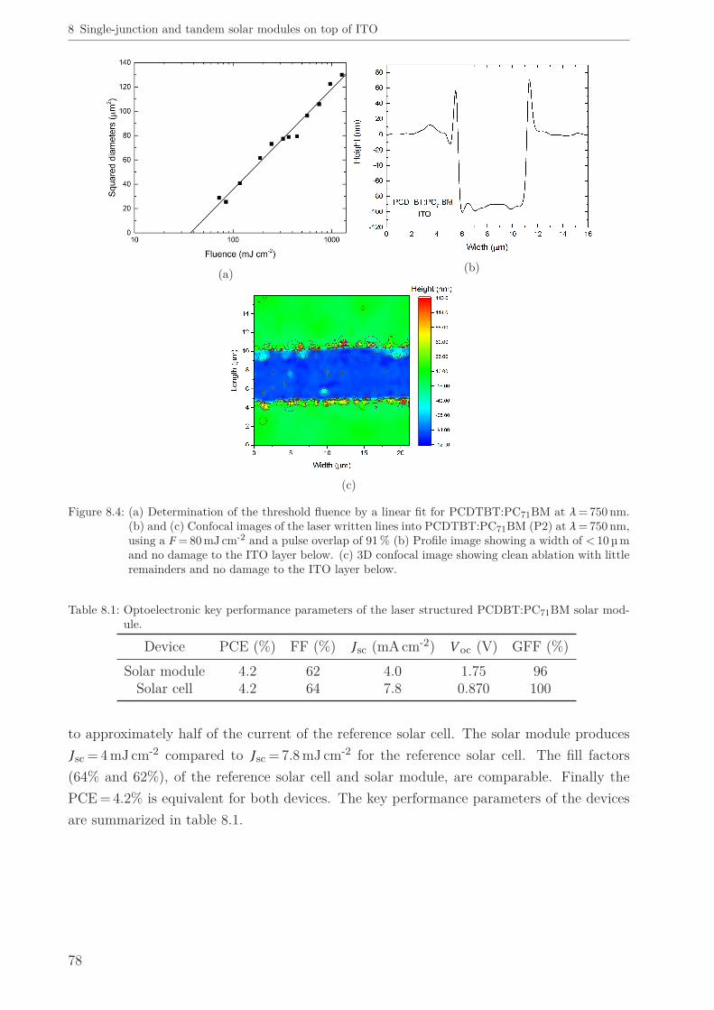
8 Single-junction and tandem solar modules on top of ITO
(a) (b)
(c)
Figure 8.4: (a) Determination of the threshold fluence by a linear fit for PCDTBT:PC71BM at λ= 750 nm.(b) and (c) Confocal images of the laser written lines into PCDTBT:PC71BM (P2) at λ= 750 nm,using a F = 80 mJ cm-2 and a pulse overlap of 91 % (b) Profile image showing a width of < 10 µ mand no damage to the ITO layer below. (c) 3D confocal image showing clean ablation with littleremainders and no damage to the ITO layer below.
Table 8.1: Optoelectronic key performance parameters of the laser structured PCDBT:PC71BM solar mod-ule.
Device PCE (%) FF (%) J sc (mA cm-2) V oc (V) GFF (%)
Solar module 4.2 62 4.0 1.75 96Solar cell 4.2 64 7.8 0.870 100
to approximately half of the current of the reference solar cell. The solar module producesJ sc = 4 mJ cm-2 compared to J sc = 7.8 mJ cm-2 for the reference solar cell. The fill factors(64% and 62%), of the reference solar cell and solar module, are comparable. Finally thePCE = 4.2% is equivalent for both devices. The key performance parameters of the devicesare summarized in table 8.1.
78

8.3 Solar modules with nanoparticulate P3HT:IC60BA
Figure 8.5: J-V curves of the best solar module and reference single-junction solar cell usingPCDTBT:PC71BM as photoactive layer.
8.3 Solar modules with nanoparticulate P3HT:IC60BAThe use of nanoparticles dispersed in alcohol or water represents an ecofriendly alternative tothe use of harmful solvents like chlorobenzene or dichlorobenzene to fabricate organic solarcells. This is specially important for the future industrial production of organic solar cells, asthe use of toxic solvents may increase the production costs, making them less competitive.Highly efficient organic solar cells, using P3HT:ICBA nanoparticles dispersed in ethanol,have been demonstrated before.108 The devices have also been upscaled to areas larger than1 cm2 using doctor blading.109
8.3.1 Architecture and solar module design
Figure 8.6a shows the architecture used for the solar module with the P1, P2 and P3 struc-turing steps. The P3HT:IC60BA devices were built using an inverted architecture with ZnOand MoO3 as ETL and HTL respectively. ITO and silver are used for the bottom and topelectrodes. The main difference to the structuring process of PCDTBT:PC71BM solar mod-ules is that, here, the ITO and ZnO were structured together as the P1 step. In this sectiontwo solar module designs were used: a design with a photoactive area of 10.5 mm2 depictedon figure 8.3b and a larger substrate (25 x 25 mm2) with a photoactive area of 1.8 cm2 (Figure8.6b). The ITO and ZnO layers have an additional laser-written line that allows contactwith the top electrode without shortening the device.
8.3.2 Threshold fluences
The ITO and silver threshold fluences were calculated in section 7.2. The threshold fluencefor the P3HT:IC60BA photoactive layer was determined using the Liu method (section 5.4).
79
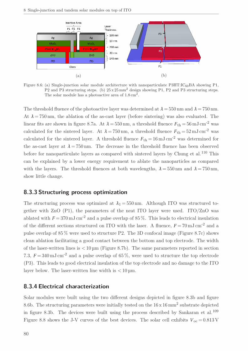
8 Single-junction and tandem solar modules on top of ITO
(a) (b)
Figure 8.6: (a) Single-junction solar module architecture with nanoparticulate P3HT:IC60BA showing P1,P2 and P3 structuring steps. (b) 25 x 25 mm2 design showing P1, P2 and P3 structuring steps.The solar module has a photoactive area of 1.8 cm2.
The threshold fluence of the photoactive layer was determined at λ= 550 nm and λ= 750 nm.At λ= 750 nm, the ablation of the as-cast layer (before sintering) was also evaluated. Thelinear fits are shown in figure 8.7a. At λ= 550 nm, a threshold fluence F th = 56 mJ cm-2 wascalculated for the sintered layer. At λ= 750 nm, a threshold fluence F th = 52 mJ cm-2 wascalculated for the sintered layer. A threshold fluence F th = 16 mJ cm-2 was determined forthe as-cast layer at λ= 750 nm. The decrease in the threshold fluence has been observedbefore for nanoparticulate layers as compared with sintered layers by Chung et al.110 Thiscan be explained by a lower energy requirement to ablate the nanoparticles as comparedwith the layers. The threshold fluences at both wavelengths, λ= 550 nm and λ= 750 nm,show little change.
8.3.3 Structuring process optimization
The structuring process was optimized at λ1 = 550 nm. Although ITO was structured to-gether with ZnO (P1), the parameters of the neat ITO layer were used. ITO/ZnO wasablated with F = 370 mJ cm-2 and a pulse overlap of 85 %. This leads to electrical insulationof the different sections structured on ITO with the laser. A fluence, F = 70 mJ cm-2 and apulse overlap of 85 % were used to structure P2. The 3D confocal image (Figure 8.7c) showsclean ablation facilitating a good contact between the bottom and top electrode. The widthof the laser-written lines is < 10 µm (Figure 8.7b). The same parameters reported in section7.3, F = 340 mJ cm-2 and a pulse overlap of 65 %, were used to structure the top electrode(P3). This leads to good electrical insulation of the top electrode and no damage to the ITOlayer below. The laser-written line width is < 10 µm.
8.3.4 Electrical characterization
Solar modules were built using the two different designs depicted in figure 8.3b and figure8.6b. The structuring parameters were initially tested on the 16 x 16 mm2 substrate depictedin figure 8.3b. The devices were built using the process described by Sankaran et al.109
Figure 8.8 shows the J-V curves of the best devices. The solar cell exhibits V oc = 0.813 V
80

8.3 Solar modules with nanoparticulate P3HT:IC60BA
(a) (b)
(c)
Figure 8.7: (a) Linear fits to determine the threshold fluences of P3HT:IC60BA (P2) at λ= 550 nm andλ= 750 nm. At λ= 750 nm the threshold fluence was calculated for both as cast and sinteredlayers. The as-cast layer shows a significant decrease of the threshold fluence. Both annealedthreshold fluences at λ= 550 nm and λ= 750 nm are similar. (b) and (c) Confocal images forthe structuring of P3HT:IC60BA (P2) at λ= 550 nm with F = 70 mJ cm-2 and a pulse overlap of85 % (b) Profile image showing a width of < 10 µ m and no damage to the ITO layer below. (c)3D image showing clean ablation with little remainders and no damage to the ITO layer belowallowing a good connection between the electrodes of two neighboring solar cells.
compared to a V oc = 1.620 V of the solar modules. The V oc doubling reflects the workingmonolithic connection between the individual solar cells. The short-circuit current densitywas J sc = 3.2 mA cm-2 for the solar module and J sc = 8.9 mA cm-2 for the solar cell. A highercurrent density of J sc = 4.5 mA cm-2 was expected for the solar module. The current densityloss can be explained by the different areas of the connected solar cells. The smaller solarcell limited the current density of the whole device. This translates into a lower PCE asthe solar cell exhibits a PCE = 3.8% compared to a PCE = 2.8% of the solar modules. Thefill factor F F = 57% is slightly better for the solar modules than the F F = 53 % for the solarcells. The change on fill factor may be attributed to the lower current density of the solarmodule. The small solar modules have a GFF = 96%.The solar module’s photoactive area was upscaled to 1.8 cm2 using the design depicted infigure 8.6b. The devices were built using doctor blading as described by Sankaran et al.109
Figure 8.8 shows the J-V curves for the solar modules composed of two solar cells. The solar
81
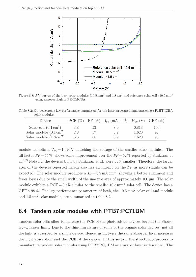
8 Single-junction and tandem solar modules on top of ITO
Figure 8.8: J-V curves of the best solar modules (10.5 mm2 and 1.8 cm2 and reference solar cell (10.5 mm2
using nanoparticulate P3HT:ICBA.
Table 8.2: Optoelectronic key performance parameters for the laser structured nanoparticulate P3HT:ICBAsolar modules.
Device PCE (%) FF (%) J sc (mA cm-2) V oc (V) GFF (%)
Solar cell (0.1 cm2) 3.8 53 8.9 0.813 100Solar module (0.1 cm2) 2.8 57 3.2 1.620 96Solar module (1.8 cm2) 3.5 55 3.9 1.620 98
module exhibits a V oc = 1.620 V matching the voltage of the smaller solar modules. Thefill factor F F = 55 %, shows some improvement over the F F = 52 % reported by Sankaran etal.109 Notably, the devices built by Sankaran et al. were 33 % smaller. Therefore, the largerarea of the devices reported herein also has an impact on the F F as more shunts can beexpected. The solar module produces a J sc = 3.9 mA cm-2, showing a better alignment andfewer losses due to the small width of the inactive area of approximately 100 µm. The solarmodule exhibits a PCE = 3.5% similar to the smaller 10.5 mm2 solar cell. The device has aGFF > 98 %. The key performance parameters of both, the 10.5 mm2 solar cell and moduleand 1.5 cm2 solar module, are summarized in table 8.2.
8.4 Tandem solar modules with PTB7:PC71BMTandem solar cells allow to increase the PCE of the photovoltaic devices beyond the Shock-ley–Queisser limit. Due to the thin-film nature of some of the organic solar devices, not allthe light is absorbed by a single device. Hence, using twice the same absorber layer increasesthe light absorption and the PCE of the device. In this section the structuring process tomanufacture tandem solar modules using PTB7:PC71BM as absorber layer is described. The
82

8.4 Tandem solar modules with PTB7:PC71BM
increase of the layer thickness of tandem devices, represent a challenge to remove the activelayers and connect the neighboring solar cells into a module.
8.4.1 Architecture and solar module design
The architectures used for the single-junction and tandem solar modules are shown in figure8.9. The tandem architecture is composed of two PTB7:PC71BM solar cells connectedthrough a recombination layer. A solvent barrier enables the deposition of the second solarcell. Here, PEDOT:PSS M-HTL Solar was used as solvent barrier. A second PEDOT:PSSformulation CPP 105D is used to improve the adherence of the M-HTL Solar layer on theabsorber layer. ZnO and MoO3 are used as ETL and HTL, respectively.
8.4.2 Threshold fluences
The ITO and silver threshold fluences were calculated in section 7.2. The threshold flu-ences for the single-junction and tandem active layers were determined at λ= 550 nm andλ= 750 nm using the Liu method (section 5.4). The threshold fluences at λ= 550 nm wereF th = 35 mJ cm-2 for the single-junction absorber layer and F th = 60 mJ cm-2 for the tandemabsorber layer (Figure 8.10a). The threshold fluences at λ= 750 nm were F th = 40 mJ cm-2
for the single-junction absorber layer and F th = 90 mJ cm-2 for the tandem absorber layer.The difference between the wavelengths could be caused by the change in the absorptionfor PTB7:PC71BM as the absorption is slightly higher at λ= 550 nm than at λ= 750 nm.111
The difference between the single-junction and the tandem absorber layer threshold fluencesis due to the layer thickness difference.
(a) (b)
Figure 8.9: (a) Single-junction solar module architecture with P1, P2 and P3 structuring steps. (b) Tandemsolar module architecture with P1, P2 and P3 structuring steps.
83

8 Single-junction and tandem solar modules on top of ITO
8.4.3 Structuring process optimization
The process parameters were optimized at λ= 550 nm. ITO/ZnO layer (P1) was structuredusing the parameters used in section 8.3. The optimized parameters to structure the pho-toactive layer (P2) are F = 13 J cm-2 and a pulse overlap of 85 % for the single-junction solarmodules, and F = 15 J cm-2 and a pulse overlap of 89 % for the tandem solar modules.The fluence and pulse overlap are slightly higher for the tandem devices to guarantee aclean ablation with negligible remainders (Figure 8.10c). The P2 structuring confocal profileimage of the tandem device is shown in Figure 8.10b. There is no visible damage to theITO underneath. Although the bulges are higher than 500 nm, they do not hamper theperformance of the devices as no shorts can be created. The laser-written line width is< 10 µm. To structure the silver/MoO3 (P3) electrodes the same parameters as for thepreviously described single-junction modules were used (sections 8.2 and 8.3). The laser-written line into silver shows complete removal of the silver top electrode. However, thephotoactive layer is not entirely removed on the tandem device.
(a) (b)
(c)
Figure 8.10: (a) Linear fits to determine the threshold fluences of PTB7:PC71BM in single-junction (contin-uous line) and tandem (dashed lines) devices at λ= 550 nm (green) and λ= 750 nm (red). (b)and (c) Confocal images of the laser-written line into the active layer (P2) in a tandem deviceat λ= 550 nm with F = 15 mJ cm-2 pulse overlap of 89% (b) Profile image showing a width of< 10 µm and no damage to the ITO layer below. (c) 3D confocal image showing clean ablationwith no remainders and no damage to the ITO layer below.
84

8.4 Tandem solar modules with PTB7:PC71BM
8.4.4 Electrical characterization
Single-junction and tandem solar modules were built using the 16 x 16 mm2 design shownin figure 8.3b. J-V curves for both single-junction and tandem solar cell and modules aredepicted in figure 8.11. The voltage doubling due to the monolithic connection is evidentas the single-junction solar modules exhibit a V oc = 1.451 V while the single-junction solarcells exhibit a V oc = 0.720 V. The solar tandem devices exhibit the voltage doubling as well.The tandem solar cells exhibit a V oc = 1.285 V and the tandem solar modules exhibit aV oc = 2.476 V. The tandem devices show a voltage loss when compared to the single-junctiondevices. This is probably due to water adsorption in the PEDOT:PSS layer during thestructuring process. PEDOT:PSS is a hygroscopic material, and it has been demonstratedthat this leads to water absorption and the degradation of the devices.112 This effect isalso reflected in the lower fill factor of the tandem reference solar cell (F F = 48%) andsolar module (F F = 44%). The tandem solar cell exhibits PCE = 4.6 % and the tandemsolar solar module exhibits PCE = 4.0 %. The single-junction solar cell and solar moduleexhibit PCE = 5.7 % and PCE = 5.5 %, respectively. Single-junction and tandem deviceswere completely built under nitrogen atmosphere with no exposition to air. The single-junction solar cells in nitrogen exhibit a PCE = 6.0 % and the tandem solar cells exhibita PCE = 6.4 % for the tandem solar cells. The PCE reduction caused by air exposition ishigher on the tandem devices that have the PEDOT:PSS layers than on the single-junctionlayers. The single junction solar modules have a GFF = 96% and the tandem solar moduleshave a GFF = 93%. The difference is due to the manual alignment of the devices on theXYZ stage of the workstation that leads to different inactive areas. The key performanceparameters of the devices are summarized in table 8.3.
Figure 8.11: J-V curves for the single-junction, tandem solar cells and modules.
85

8 Single-junction and tandem solar modules on top of ITO
Table 8.3: Key performance parameters for the laser structured single-junction and tandem solar modulesand reference cells using PTB7:PC71BM as absorber layer.
Solar devices PCE (%) FF (%) J sc (mA cm-2) V oc (V) GFF (%)
Single cell (Nitrogen) 6.0 60 14.1 0.720 100Single cell (Air) 5.7 62 12.8 0.723 100Single module (Air) 5.5 66 5.8 1.450 96Tandem cell (Nitrogen) 6.4 53 8.3 1.460 100Tandem cell (Air) 4.6 48 7.5 1.285 100Tandem module (Air) 4.0 44 3.6 2.476 93
8.5 Rapid experimental optimization of the solar cell widthThe width of each solar cell is very important for the final performance of a solar module.If the solar cell is too wide, the performance decreases due to the resistive losses in theelectrode. If the solar cell is too narrow, a larger number of monolithic connections isnecessary, resulting in an increase of the inactive area of the device. Hence, a compromise isnecessary, and the width and number of solar cells in a module should be optimized. Thishas been accomplished using simulation methods where the resistance of the electrodes isestimated.95
P1 3. P3
1., 2. P2
P1 3. P3
1., 2. P2Figure 8.12: Substrate design for the solar cell width optimization. Initially the ITO is structured for different
solar cell widths. The photoactive layer is coated and P2 is structured. The top electrode iscoated and P3 is structured. The width of each of the solar cells is determined by the positionof the monolithic connection. The solar cells are measured through the monolithic connection,hence considering the inactive area in the measurements. The solar cell widths are shown inorange.113
86
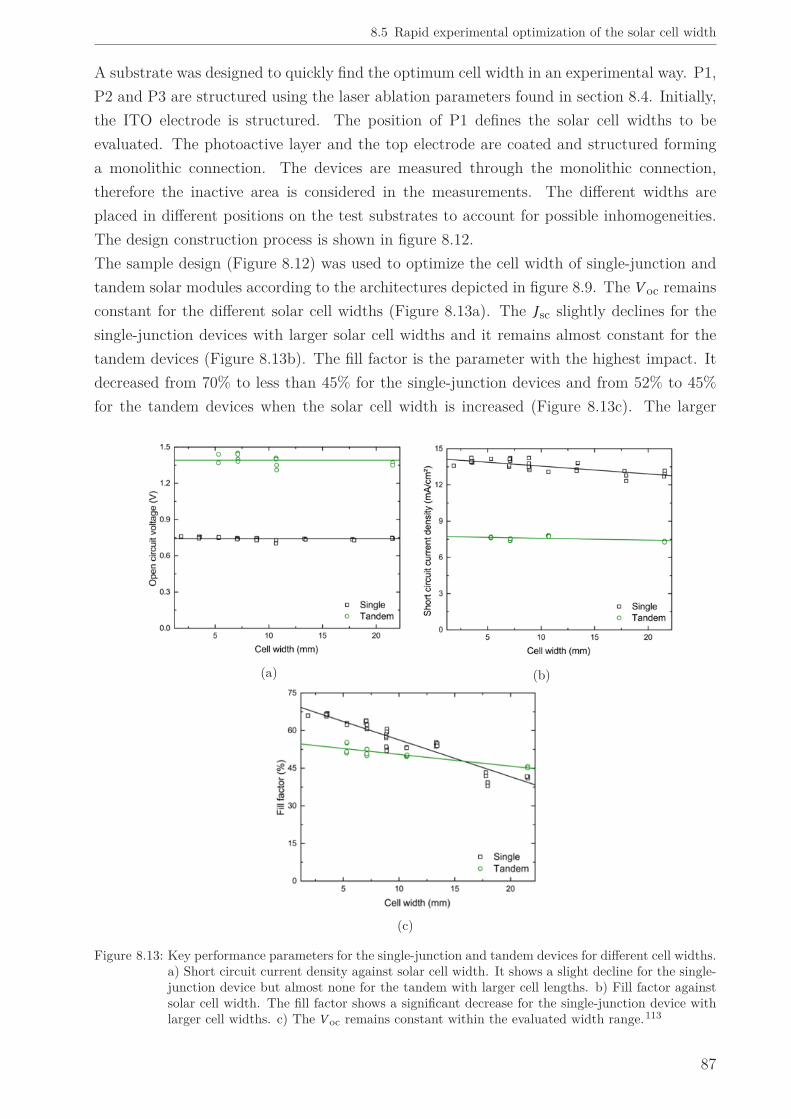
8.5 Rapid experimental optimization of the solar cell width
A substrate was designed to quickly find the optimum cell width in an experimental way. P1,P2 and P3 are structured using the laser ablation parameters found in section 8.4. Initially,the ITO electrode is structured. The position of P1 defines the solar cell widths to beevaluated. The photoactive layer and the top electrode are coated and structured forminga monolithic connection. The devices are measured through the monolithic connection,therefore the inactive area is considered in the measurements. The different widths areplaced in different positions on the test substrates to account for possible inhomogeneities.The design construction process is shown in figure 8.12.The sample design (Figure 8.12) was used to optimize the cell width of single-junction andtandem solar modules according to the architectures depicted in figure 8.9. The V oc remainsconstant for the different solar cell widths (Figure 8.13a). The J sc slightly declines for thesingle-junction devices with larger solar cell widths and it remains almost constant for thetandem devices (Figure 8.13b). The fill factor is the parameter with the highest impact. Itdecreased from 70% to less than 45% for the single-junction devices and from 52% to 45%for the tandem devices when the solar cell width is increased (Figure 8.13c). The larger
(a) (b)
(c)
Figure 8.13: Key performance parameters for the single-junction and tandem devices for different cell widths.a) Short circuit current density against solar cell width. It shows a slight decline for the single-junction device but almost none for the tandem with larger cell lengths. b) Fill factor againstsolar cell width. The fill factor shows a significant decrease for the single-junction device withlarger cell widths. c) The V oc remains constant within the evaluated width range.113
87

8 Single-junction and tandem solar modules on top of ITO
(a) (b)
Figure 8.14: a) Number of structuring steps and PCE versus cell width. b) J-V curves of the reference solarcell (10.5 mm2) and the eight-cell-solar module (6.5 cm2) built with the previously determinedsolar cell width. The solar module has 87 % of the reference solar cell PCE.113
reduction for the single devices stems from the larger operating currents that increase theohmic losses.Solar modules were built to prove the previous findings focusing on the single-junction devicesas they showed the higher decline. Figure 8.14a shows that the maximum PCE is achievedwith a solar cell width of 2.4 mm. However, this requires the maximum number of monolithicconnections, hence of laser structuring steps. A solar cell width of 6 mm will yield 90% of themaximum PCE, but will require 34% less structuring steps resulting in a reasonable exchangethat will ease the fabrication of the devices.The decrease in the number of processing stepsmay also lead to a higher yield as there are fewer possibilities of defects.Solar modules were then built with a total photoactive area of 6.5 cm2. The J-V curvesfor both the reference solar cell (10.5 mm2) and the solar module are shown in figure 8.14b.The solar module has PCE = 5.0% and the reference solar cell has PCE = 5.7% (Figure8.14b). The ratio between both PCEs is 87% demonstrating the accuracy of the experimentalmethod (90% was predicted). The slightly lower PCE can be explained due to the largerarea (6.5 cm2) leading to more inhomogeneities of the layers. The solar modules have aGFF = 99% demonstrating the reduction of the lost area with the use of lasers.
8.6 DiscussionIn this chapter, laser structuring of monolithic connections to construct organic solar mod-ules was demonstrated. The devices were built using three different photoactive layers,PCDTBT:PC71BM, nanoparticulate P3HT:IC60BA and PTB7:PC71BM in single-junctionand tandem architectures. Table 8.4 shows a summary of the threshold fluences of thesematerials.The threshold fluence of the single-junction devices, using PCDTBT:PC71BM andPTB7:PC71BM, are similar (35 and 41 mJ cm-2). The threshold fluence of the sintered
88

8.6 Discussion
Table 8.4: Threshold fluences of the photoactive layers PCDTBT:PC71BM, nanoparticulate P3HT:IC60BAand PTB7:PC71BM in single-junction and tandem architectures.
Material λ= 550 nm (mJ cm-2) λ= 750 nm (mJ cm-2)
PCDTBT:PC71BM - 40P3HT:IC60BA sintered 56 52P3HT:IC60BA as-cast - 16
PTB7:PC71BM single-junction 35 41PTB7:PC71BM tandem 60 90
P3HT:IC60BA nanoparticulate layer is slightly higher. This could be caused by the thickerlayer of P3HT:IC60BA (200 nm). The as-cast P3HT:IC60BA nanoparticulate layer has asignificantly lower threshold, as the nanoparticles are easier to ablate as shown by byChung et al.110. The effect of the wavelength is evident on the PTB7:PC71BM layers,both single-junction and tandem. The increase at λ= 750 nm may be originated from thesharp absorption reduction of the layer.Ultrashort pulsed lasers are suitable to structure solar modules using ITO as bottom elec-trode on a glass substrate. The large working window between the threshold fluence ofITO (P1) and the threshold fluence of the photoactive layers (P2), facilitates the selectiveablation of the P2 layer. Although the silver (P3) has a higher threshold fluence than theITO (Figure 7.3a), the ablation without damage to the ITO is possible when working witha fluence close to the threshold fluence of silver and a low pulse overlap.Finally, the use of ultrashort pulsed lasers facilitate the experimental optimization of the solarmodules. One substrate is enough to test and to find the most adequate solar cell widthin terms of PCE and number of processing steps. The PCE of the test solar module was87 % of the PCE of the reference solar cell (Maximum expected PCE). The prediction of theexperiment was 90%. The small difference can be explained due to the larger photoactivearea of the test solar modules. The GFF of these devices was higher than 99 % againdemonstrating the advantages of using ultrashort pulsed lasers.
89

9 All-solution semi-transparent modules
ITO has been the most used semi-transparent electrode in OPV. However, it has severaldisadvantages, as it cannot be produced through a roll-to-roll process and it is highly brittlewhich limits its applicability in mechanically flexible devices, which is one of the inherentadvantages of OPV. Likewise, the use of vacuum processed metal top electrodes hinders theimplementation of a full roll-to-roll process that will decrease the future price of OPV. Severalalternatives have been studied to substitute both electrodes, such as metal inks,114–117 silvernanowires,117–122 high conductive polymers,121–124 metal grids125 and hybrids.126–132 All-solution solar modules have also been constructed following this concept,117 however P1, P2and P3 have been mechanically scribed leading to low geometric fill factors and imprecisiondue to the manual processes performed to structure.In this chapter ultrashort pulse lasers were used to structure a flexible all-solution solarmodule. The materials and the device architecture are described in section 9.1. In section9.2 the threshold fluences for the different materials is determined. Section 9.3 describesthe ablation process for certain wavelengths and in section 9.4 the construction of a laserstructured solar module is described. Section 9.5 provides a short discussion of the resultsdepicted in this chapter. This results depicted in this chapter were part of the master thesisof Torsten Friedrich. The device architecture was developed by Jens Czolk, Manuel Koppitzand Dominik Landerer.132
9.1 Materials and architecture
9.1.1 Materials
ZnO was used as ETL, and the material is described in section 7.1. PEDOT:PSS is used toimprove the lateral conductivity of the silver mesh on PET used in this chapter. PEDOT:PSSis described in section 8.1.
PET foil with silver mesh
A 50 µm thick PET foil with 10 µm wide and 40 nm thick printed silver lines was used asbottom electrode. The silver mesh covers 9 % of the PET substrate as depicted on figure9.1a. The silver mesh electrode has a sheet resistance R = 16Ω-1 which is comparableto that of ITO on glass and lower than that of ITO on PET. The transmission of the PET
91

9 All-solution semi-transparent modules
with the silver grid is close to 80 % as shown in figure 9.1b. When combined with a layer ofPEDOT:PSS the transmission declines slightly in the infrared spectral regime.
Hybrid electrodes (HYE) comprising PEDOT:PSS and silver nanowires
A commercially available solution of PEDOT:PSS mixed with silver nanowires (Clevios HYE)was used as one of the electrodes. The nanowire diameter was estimated to be approximately20 nm. They have an average length of 20 µm. The sheet resistance of the correspondingelectrodes are dependent on the thickness. Therefore a compromise between sheet resistanceand transmission of the layer is necessary (Figure 9.1d). Figure 9.1c shows an SEM image ofthe nanowires combined with PEDOT:PSS. The nanowires are homogeneously distributed.
PBTZT-stat-BDTT-8
PBTZT-stat-BDTT-8 is a royal blue polymer with absorption peaks at λ= 600 nm andλ= 640 nm. It is composed of substituted benzodithiophene, thiophene, and benzothiadia-zole. The LUMO and HOMO are reported to be -3.7 and -5.4 eV, respectively. The materialhas demonstrated PCE = 4.5% for semi-transparent flexible devices. It was used on the con-
(a) (b)
(c) (d)
Figure 9.1: (a) Silver grid optical microscope image. (b) Transmission of the silver grid alone and in combina-tion with PEDOT:PSS.(c) SEM image of the HYE electrode. The nanowires are homogeneouslydistributed inside the PEDOT:PSS layer. (d) Transmission and sheet resistance versus layerthickness of the HYE electrode.132
92

9.1 Materials and architecture
struction of the ”Solar Tree”, an exhibition showing the potential of OPV during the ExpoMilan, 2015.133
PC60BM
[6,6]-phenyl C61 butyric acid methyl ester (PC60BM) is a fullerene derivative that is one ofthe most common acceptor materials used in OPV research. It was first discovered in 1995as soluble derivative of C60.134 The LUMO and HOMO level are reported to be -4.3 and-6.0 eV respectively.16 It has a moderate absorption and therefore does not contribute to thegeneration of electron-hole pairs in the organic solar cell.
techPCBM
techPCBM is a combination of PC60BM and PC71BM with a ratio of 9:1. The materialpossesses some of the advantages of PC71BM (section 8.1). The combination with PC60BMreduces the price, making it more suitable for future large scale industrial applications.
9.1.2 Architecture
An inverted architecture was used to build semi-transparent solar modules. The silver gridin combination with PEDOT:PSS form the bottom electrode. For the construction of thesolar modules the silver grid was pre-structured during the printing process. Hence thestructuring efforts were focused on the selective ablation of the PEDOT:PSS layer. ZnO isused as ETL and together with PBTZT-stat-BDTT-8:techPCBM is structured as P2. HYElayer is used as top electrode. No extra HTL was used, as PEDOT:PSS is a common HTL
Figure 9.2: Semi-transparent solar module architecture with layer thicknesses and P1, P2 and P3 structuringsteps. The bottom electrode is a hybrid electrode composed of a silver grid and PEDOT:PSS. PE-DOT:PSS is structured as P1 using the ultrashort pulsed laser. The silver grid is pre structured.ZnO is used as ETL and together with the BTZT-stat-BDTT-8:techPCBM layer, it is structuredduring the P2 step. Finally the top electrode is fabricated from HYE and it is structured as P3.
93
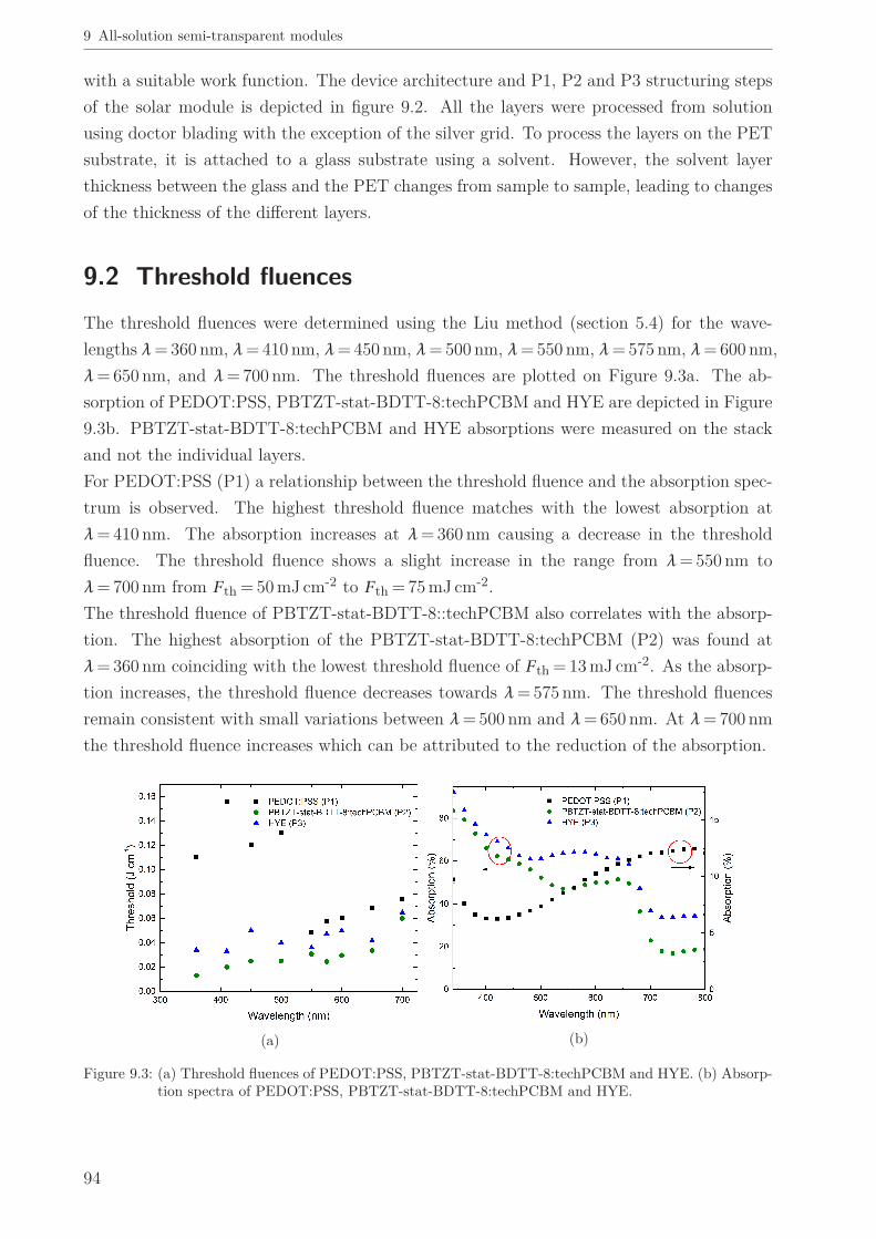
9 All-solution semi-transparent modules
with a suitable work function. The device architecture and P1, P2 and P3 structuring stepsof the solar module is depicted in figure 9.2. All the layers were processed from solutionusing doctor blading with the exception of the silver grid. To process the layers on the PETsubstrate, it is attached to a glass substrate using a solvent. However, the solvent layerthickness between the glass and the PET changes from sample to sample, leading to changesof the thickness of the different layers.
9.2 Threshold fluencesThe threshold fluences were determined using the Liu method (section 5.4) for the wave-lengths λ= 360 nm, λ= 410 nm, λ= 450 nm, λ= 500 nm, λ= 550 nm, λ= 575 nm, λ= 600 nm,λ= 650 nm, and λ= 700 nm. The threshold fluences are plotted on Figure 9.3a. The ab-sorption of PEDOT:PSS, PBTZT-stat-BDTT-8:techPCBM and HYE are depicted in Figure9.3b. PBTZT-stat-BDTT-8:techPCBM and HYE absorptions were measured on the stackand not the individual layers.For PEDOT:PSS (P1) a relationship between the threshold fluence and the absorption spec-trum is observed. The highest threshold fluence matches with the lowest absorption atλ= 410 nm. The absorption increases at λ= 360 nm causing a decrease in the thresholdfluence. The threshold fluence shows a slight increase in the range from λ= 550 nm toλ= 700 nm from F th = 50 mJ cm-2 to F th = 75 mJ cm-2.The threshold fluence of PBTZT-stat-BDTT-8::techPCBM also correlates with the absorp-tion. The highest absorption of the PBTZT-stat-BDTT-8:techPCBM (P2) was found atλ= 360 nm coinciding with the lowest threshold fluence of F th = 13 mJ cm-2. As the absorp-tion increases, the threshold fluence decreases towards λ= 575 nm. The threshold fluencesremain consistent with small variations between λ= 500 nm and λ= 650 nm. At λ= 700 nmthe threshold fluence increases which can be attributed to the reduction of the absorption.
(a) (b)
Figure 9.3: (a) Threshold fluences of PEDOT:PSS, PBTZT-stat-BDTT-8:techPCBM and HYE. (b) Absorp-tion spectra of PEDOT:PSS, PBTZT-stat-BDTT-8:techPCBM and HYE.
94

9.3 Structuring process optimization
The threshold fluences of HYE follows a similar pattern with the minimum located atλ= 360 nm and λ= 410 nm with F th = 34 mJ cm-2 and F th = 33 mJ cm-2 respectively. Thethreshold fluence F th = 50 mJ cm-2 at λ= 450 nm. The threshold fluence shows slight changesbetween λ= 550 nm and λ= 650 nm. At λ= 700 nm there is again an increase following theabrupt reduction in the absorption.The threshold fluence for the three layers do not match equations 5.9 and 5.10. The equa-tions predicted a linear relationship between the threshold fluence and the wavelength. Thedifferent observation may originate from the thin-film nature and the transparency of thematerials as the equations were developed using the assumptions of having bulk materialsand surface processes.
9.3 Structuring process optimizationAs PEDOT:PSS is an important material that is commonly used in organic electronics,here the ablation results are shown for three different wavelengths, λ= 360 nm, λ= 450 nmand λ= 600 nm. A single wavelength, λ= 600 nm, was studied to ablate PBTZT-stat-BDTT-8:techPCBM (P2) and HYE (P3). λ= 600 nm was chosen as the PBTZT-stat-BDTT-8:tech-PCBM (P2) photoactive layer exhibits the highest absorption in this point.
9.3.1 PEDOT:PSS structuring (P1)
Fluences close to the threshold fluence were tested using different stage speeds, thus changingthe pulse overlap to find the adequate structuring parameters. The bottom electrode is com-posed of the silver grid and a layer of PEDOT:PSS. The silver grid was pre-structured. There-fore, the focus was on the structuring of PEDOT:PSS to complement the pre-structuringprocess. One of the requirements to structure PEDOT:PSS is to diminish the damage onthe PET layer following the considerations in chapter 6. A second structuring requirementis to produe the bulges below 200 nm to prevent shorts with the top electrode. Finally, it isimportant to completely remove the PEDOT:PSS layer to electrically insulate the two solarcells.PEDOT:PSS has been previously structured using laser ablation. Semaltianos et al. useda picosecond laser to structure PEDOT:PSS on top of glass.135 Photomechanical ablationwas identified as the possible ablation mechanism. The threshold fluence was calculated atF th = 130 mJ cm-2 for λ= 1064 nm, with 10 ps pulses and layers with a thickness of 100 nm.No measurements of the bulge height were provided for the laser-written lines. Schoonder-beek et al. tested the ablation of PEDOT:PSS on top of PET with both ns and ps lasersources.136 The ns pulses achieved no optimized ablation and formed melted lines. The pspulses at λ= 1030 nm and λ= 515 nm resulted in complete removal of the PEDOT:PSS.
95
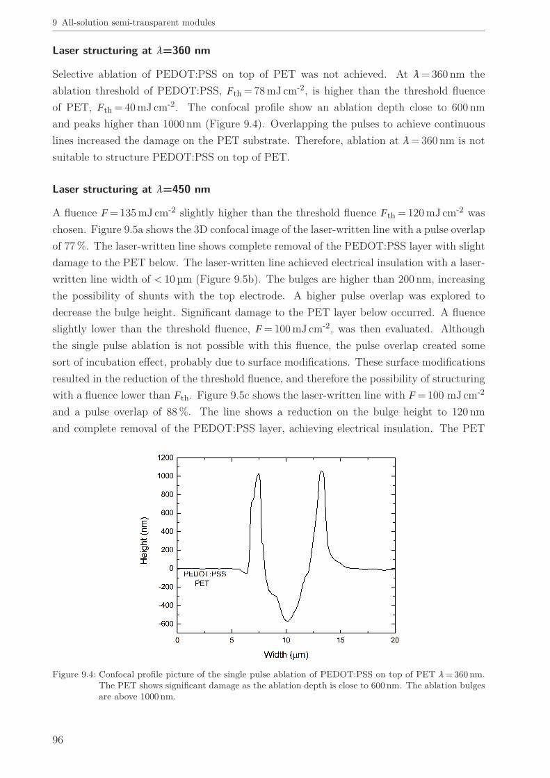
9 All-solution semi-transparent modules
Laser structuring at λ=360 nm
Selective ablation of PEDOT:PSS on top of PET was not achieved. At λ= 360 nm theablation threshold of PEDOT:PSS, F th = 78 mJ cm-2, is higher than the threshold fluenceof PET, F th = 40 mJ cm-2. The confocal profile show an ablation depth close to 600 nmand peaks higher than 1000 nm (Figure 9.4). Overlapping the pulses to achieve continuouslines increased the damage on the PET substrate. Therefore, ablation at λ= 360 nm is notsuitable to structure PEDOT:PSS on top of PET.
Laser structuring at λ=450 nm
A fluence F = 135 mJ cm-2 slightly higher than the threshold fluence F th = 120 mJ cm-2 waschosen. Figure 9.5a shows the 3D confocal image of the laser-written line with a pulse overlapof 77 %. The laser-written line shows complete removal of the PEDOT:PSS layer with slightdamage to the PET below. The laser-written line achieved electrical insulation with a laser-written line width of < 10 µm (Figure 9.5b). The bulges are higher than 200 nm, increasingthe possibility of shunts with the top electrode. A higher pulse overlap was explored todecrease the bulge height. Significant damage to the PET layer below occurred. A fluenceslightly lower than the threshold fluence, F = 100 mJ cm-2, was then evaluated. Althoughthe single pulse ablation is not possible with this fluence, the pulse overlap created somesort of incubation effect, probably due to surface modifications. These surface modificationsresulted in the reduction of the threshold fluence, and therefore the possibility of structuringwith a fluence lower than F th. Figure 9.5c shows the laser-written line with F = 100 mJ cm-2
and a pulse overlap of 88 %. The line shows a reduction on the bulge height to 120 nmand complete removal of the PEDOT:PSS layer, achieving electrical insulation. The PET
Figure 9.4: Confocal profile picture of the single pulse ablation of PEDOT:PSS on top of PET λ= 360 nm.The PET shows significant damage as the ablation depth is close to 600 nm. The ablation bulgesare above 1000 nm.
96

9.3 Structuring process optimization
(a) (b)
(c) (d)
Figure 9.5: (a) and (b) 3D confocal image and profile for the laser-written line on PEDOT:PSS at λ= 450 nm,F = 130 mJ cm-2 and pulse overlap of 77%. The line shows slight damage to the PET substratebelow. The bulge height is 200 nm. (c) and (d) 3D confocal image and profile for the laser-writtenline on PEDOT:PSS at λ= 450 nm, F = 100 mJ cm-2 and pulse overlap of 88 %. The increase inpulse overlap leads to lower bulge height (120 nm) with negligible damage to the pet substratebelow.
substrate before shows little damage with a laser-written line width of < 10 µm (Figure 9.5d).The increase in pulse overlap resulted in lower bulges on the laser-written lines.
Laser structuring at λ=600 nm
A fluence F = 100 mJ cm-2 higher than the threshold fluence F th = 60 mJ cm-2 was chosen atλ= 600 nm. Figure 9.6a shows the 3D confocal image of the laser-written line with a pulseoverlap of 84 %. Negligible damage to the PET substrate was produced by the laser ablation.The laser-written line has width of < 10 µm and complete removal of the PEDOT:PSS layerleading to electrical insulation of the bottom electrode. The bulges present on the line arehigher than 300 nm (Figure 9.6b) increasing the possibility of shunts with the top electrode.The pulse overlap was increased to 98%, successfully reducing the bulge height under 150 nm(Figure 9.6d). The laser-written lines show complete removal of the PEDOT:PSS layerachieving electrical insulation and a width of ≤ 10 µm. The PET substrate shows negligible
97

9 All-solution semi-transparent modules
(a) (b)
(c) (d)
Figure 9.6: (a) and (b) 3D confocal image and profile for the laser-written line into PEDOT:PSS atλ= 600 nm, F = 100 mJ cm-2 and pulse overlap of 84 %. The line shows negligible damage tothe PET substrate below. The bulge height is 300 nm. Laser-written line width is < 10 µm.(c)and (d) 3D confocal image and profile for the laser-written line into PEDOT:PSS at λ= 600 nm,F = 100 mJ cm-2 and pulse overlap of 98%. The line shows negligible damage to the PET sub-strate below. The increase in the pulse overlap leads to a reduction of the bulge to 150 nm.Laser-written line width is < 10 µm.
damage (Figure 9.6c). Similar to the case at λ= 450 nm, the increase in pulse overlap resultedin lower bulges.
9.3.2 PBTZT-stat-BDTT-8:techPCBM (P2) structuring
One of the requirements to structure PBTZT-stat-BDTT-8:techPCBM (P2) is to minimizethe damage to the PEDOT:PSS layer below. The bulge height does not play an importantrole, as they do not cause any shunt. Complete removal of the PBTZT-stat-BDTT-8:tech-PCBM (P2) improves the connection of the devices as the remaining PBTZT-stat-BDTT-8:techPCBM (P2) would increase the serial resistance hampering the performance of thedevice.
Laser structuring at λ=600 nm
The structuring of PBTZT-stat-BDTT-8:techPCBM (P2) was optimized at λ= 600 nm, us-ing a F = 30 mJ cm-2 which is slightly higher than the threshold fluence F th = 25 mJ cm-2.
98

9.3 Structuring process optimization
Figure 9.7a shows the 3D confocal image of the ablation with a pulse overlap of 75 %. Thelaser-written line has an average ablation depth of 105 nm resulting in slight damage to thePEDOT:PSS layer below. The damaged is due to melting of the PEDOT:PSS layer. Thelaser-written line width is < 5 µm (Figure 9.7b).The pulse overlap plays an important role in the selective ablation of thin-films. The pulseoverlap was evaluated from 70 % to 98 % (Figure 9.7c). Up to a pulse overlap of 87 % theablation depth is close to 100 nm, resulting in negligible damage to the PEDOT:PSS layerbelow. A pulse overlap of 90 % increases the average ablation depth to 140 nm due to thepresence of ablation on the PEDOT:PSS. A pulse overlap of 92% results in the completeremoval of the PEDOT:PSS layer below. The reason for the ablation of the layer below is theincubation effect created by the previous pulses. The incubation effects with a pulse overlaphigher than 90 % increase the absorption enough to lead to ablation of the PEDOT:PSSlayer below even when part of the energy was already used to ablate the PBTZT-stat-BDTT-8:techPCBM. These results accentuate the importance of the pulse overlap in theselective ablation of thin-films.
(a) (b)
(c)
Figure 9.7: (a) and (b) 3D confocal image and profile for the laser-written line into PBTZT-stat-BDTT-8:techPCBM at λ= 600 nm, F = 30 mJ cm-2 and pulse overlap of 70%. The line shows littledamage to the PEDOT:PSS electrode below. Laser-written line width is < 5 µm. (c) Pulseoverlap against ablation depth. A pulse overlap up to 88 % results in selective ablation of thePBTZT-stat-BDTT-8:techPCBM on top of PEDOT:PSS.
99

9 All-solution semi-transparent modules
9.3.3 HYE (P3) structuring
In order to use HYE (P3) as top electrode, it is crucial to structure the HYE layer withoutdamage to the bottom PEDOT:PSS electrode. The combination of PEDOT:PSS with silvernanowires has been previously structured. Guo et al. fabricated organic solar modules usingPEDOT:PSS with silver nanowires as top electrode and ITO/IMI as bottom electrode.137
They achieved a GFF = 95% with a PCE = 2.4% for a 3-cell solar module with an photoactivearea of 0.1 cm2.
Laser structuring at λ=600 nm
A fluence F = 30 mJ cm-2 which is below the threshold fluence F th = 50 mJ cm-2 was selected.At this fluence the pulses do not cause ablation but melt the material. Figure 9.8a shows aprocessed line with a pulse overlap of 81%.
(a) (b)
(c) (d)
Figure 9.8: (a) 3D confocal image of the laser-written line into HYE at λ= 600 nm using F = 30 mJ cm-2 anda pulse overlap of 81 %. The line shows melting of the material. (b) and (c) 3D confocal imageand profile for the structured line on HYE at λ= 600 nm, F = 30 mJ cm-2 and pulse overlap of94 %. The line shows little damage to the PEDOT:PSS layer below. Laser-written line widthis < 5 µm. (d) Pulse overlap against ablation depth. A pulse overlap below 91 % results in noablation and just melting of the material. A pulse overlap above 98% results in complete removalof the PEDOT:PSS bottom electrode.
100

9.4 Solar module characterization
The laser created a melted line with a thickness of approx. 2.5 µm. The melted materialresults in an incubation effect that causes ablation of the material when the pulse overlap isincreased. Figure 9.8b shows the laser-written line with a pulse overlap of 94 %. The ablationdepth is approximately 350 nm showing the removal of the HYE top electrode together withthe PBTZT-stat-BDTT-8:techPCBM absorption layer. Slight damage to the PEDOT:PSSmight be present. The laser-written line width is < 5 µm (Figure 9.8c). If the pulse overlapis further increased the PEDOT:PSS layer is damaged. Figure 9.8d shows the relationshipbetween the pulse overlap and the ablation depth, showing that when the pulse overlap ishigher than 98 % the PEDOT:PSS layer is completely removed.
9.4 Solar module characterizationUsing the structuring parameters described in the previous section, laser structured solarmodules were built. Each solar module is composed of two solar cells. The J-V curves of solarcells and the structured solar module are shown in figure 9.9a. The devices were measuredunder illumination through the top and bottom electrode. The voltage of the solar moduleswas twice the voltage of the single solar cells. This demonstrates the working monolithicconnection of the device. The individual devices showed a poor fill factor F F = 48%, howeverthe current density reduction on the solar module decreased the ohmic power losses leadingto an improved fill factor of F F = 53% for the device illuminated through the top electrode.This is also true for the device under illumination through the bottom electrode side wherethe fill factor improved to F F = 55%. The device exhibits a transparency of 20% with aPCE = 3.0% when illuminated through the bottom electrode. The device has a PCE = 2.6%under illumination through the top electrode. The reduction is due to the lower transmissionof the top electrode when compared with the bottom electrode, leading to a reduction in thecurrent density of the device. When comparing the efficiency of the solar module with thesolar cell a slight decrease on the efficiency is present. This is due to a slight mismatch onthe solar cells’ area due to the manual alignment of the device on the workstation.
(a) (b)
Figure 9.9: (a) J-V curves of the single solar cells and solar module illuminated through either electrode. (b)Optical microscope image of the monolithic connection of the solar module.
101

9 All-solution semi-transparent modules
Table 9.1: Key performance parameters for the semi-transparent solar module.
Device (illuminated through) PCE (%) FF (%) Jsc (mA cm-2) Voc (V)
Left subcell (Top electrode) 2.5 48 7.4 0.69Right subcell (Top electrode) 2.7 48 8.3 0.68
Module (Top electrode) 2.6 53 3.6 1.45Module (Bottom electrode) 3.0 55 4.0 1.4
The inactive area width of the device is approximately 1 mm (Figure 9.9b) leading to alow GFF. The large structuring width was caused by the prestructuring of the silver gridthat was done considering mechanical methods and no laser ablation. However, there is notechnical limitation to achieve a higher GFF. The devices have an photoactive area largerthan 1 cm2, clearly showing the possibility to upscale the devices. The key parameters forthe solar module are shown in table 9.1:
9.5 DiscussionIn this chapter, the use of femtosecond lasers to selectively structure polymer layers has beendemonstrated. All the polymer layers are coated from solution, using processes than can betransferable to industrial scale, such as doctor blading. The device exhibits a decent effi-ciency with PCE = 3 % and a transparency of 20 %. Notably, all three structuring steps wereperformed with structuring widths under 5 µm. Hence, the lines are invisible to the humaneye. The solar modules have no visible features, like bus bars or large monolithic connec-tions, making them ideal for window integration. The solar modules are also mechanicallyflexible, exhibiting most of the promising concepts behind OPV.Selective ablation of the PEDOT:PSS electrode with low bulges under 150 µm was achieved.The pulse overlap plays an important role, as higher pulse overlap leads to lower ablationbulges. PEDOT:PSS may play a role in the future for other organic electronic devices,therefore achieving selective structuring with low bulges is crucial for future production.Selective ablation of PBTZT-stat-BDTT-8:techPCBM (P2) layer on top of PEDOT:PSS wasalso demonstrated. Selective ablation of thin film polymer layers is an important milestone inthe way to roll-to-roll process of organic solar modules in the future. For HYE (P3) the layerwas ablated without damaging the PEDOT:PSS bottom electrode below, ergo preserving thefunctionality of the device.Ablation below the threshold fluence was demonstrated for PEDOT:PSS (P1) and HYE(P3). The initial pulses melt the material creating an incubation effect that increases theabsorption leading to ablation of the layers. The use of lower fluences facilitates the selectiveablation of the layers. The high overlap of picosecond pulses restricts the ablation intometal thin-films.138 However, femtosecond pulses enhance ablation even with fluences belowthe threshold fluence. Further investigations are required on this topic to determine themechanism that enhances or limits the ablation with pulse overlap.
102

9.5 Discussion
Figure 9.10: P1, P2 and P3 structuring steps on the semitransparent solar module. The solar module isall-solution on a flexible substrate. The small structured widths of P1, P2 and P3 lead to ahomogeneous surface, ideal for window integration.
The threshold fluences follows the absorption spectrum at the studied wavelengths. Thisobservation cannot be described with equations 5.9 and 5.10 where an increasing value ofthe threshold fluence with higher wavelengths is expected. The difference is due to the thinfilm nature of our layers and the semi-transparency of them, factors that were not consideredfor the previous equations. This matches the observations of chapter 7 for SuperYellow andITO on top of glass. It also matches the observations of ITO on PET (chapter 6)Although, devices using ITO as bottom electrode were previously demonstrated in this workin chapter 8. The selective ablation of polymer thin-films on top of other polymers is abigger challenge as the working windows are severely reduced. Therefore, the working solarmodule all laser structured with ultrashort pulsed lasers is an important accomplished tofabricate these devices in the future.
103


10 All-solution opaque modules
In chapter 9 the construction of all-solution semi-transparent solar modules on flexible sub-strates was demonstrated. However, several applications require a rigid glass substrate.Koppitz et al. successfully demonstrated the construction of all-solution organic solar mod-ules on glass using silver ink, as bottom electrode, and PEDOT:PSS with silver nanowires(HYE) as top electrode.117 The solar modules were structured using a lithography processfor the silver electrode (P1), manually wiping the absorber layer (P2) and by tape patterningthe HYE electrode (P3). These processes are not ideal for the future industrial fabricationof OPV.In this chapter structuring process to construct opaque all-solution solar modules on a glasssubstrate is optimized. Section 10.1 describes the silver ink used to apply the bottom electrodeand the architecture used to construct the solar modules. In section 10.2 the thresholdfluences for the different materials in the visible spectrum (λ= 360 nm to λ= 700 nm) isreported. Section 10.3 summarizes the structuring process for P1, P2 and P3. Section10.4 describes the characteristics of the laser structured solar modules. Finally, section 10.5gives the conclusions for the chapter. This chapter was done as the master thesis of TimWünnemann. The experiments were prepared in collaboration with Manuel Koppitz.
10.1Materials and device architecture
10.1.1Materials
Some of the materials used for the construction of the opaque solar modules have alreadybeen described in previous chapters. ZnO was described in section 7.1 and is used as ETL.The electron donor PBTZT-stat-BDTT-8 and the electron acceptor techPCBM that formedthe absorber layer were discussed in section 9.1. Finally, HYE used for the top electrode isalso discussed in section 9.1.
Silver
The silver layer was processed from a metal-organic decomposition (MOD) silver ink. Ithas a sheet resistance of R = 0.9Ω-1 at an optimized layer thickness of 165 nm. Theroot-mean-square roughness of the layer is approximately 3 nm. The low roughness is anecessary requirement as any spike on the silver layer might cause shunts, hence hinderingthe performance of the device. Silver has a work function of 4.3 eV.
105

10 All-solution opaque modules
Primer
A UV-curing primer (Polyprimer) was used before the application of the silver layer. Itwas diluted in 2-propanol (1:100). It can produce homogenous layers with thicknesses up to15 µm and it is non-hygroscopic. The used layer has an approximate thickness of 10 nm.
10.1.2Device architecture and design
An inverted architecture was used to construct the solar modules. It requires top illuminationas the silver bottom electrode is opaque. The first layer is a primer that flattens the substrateand improves the adhesion of the silver ink. The flat surface is important as any protuberancelarger than 200 nm may translate on a silver peak and create shunts with the top electrode.The silver works as bottom electrode, with ZnO as ETL. The absorber layer is composedof the donor-acceptor mixture of PBTZT-stat-BDTT-8:techPCBM. HYE was used as topelectrode.Silver was structured as P1. ZnO was structured together with PBTZT-stat-BDTT-8:tech-PCBM as P2. HYE was structured as P3.Figure 10.1b depicts the substrate design of the solar modules. The red area on the topelectrode illustrates the photoactive area of the device. The photoactive area is approxi-mately 1 cm2 with some variations due to the manual structuring of the top electrode. Eachsubstrate contains two solar modules. The design allows the measurement of the individualsolar cells, marked on the design as solar cell A and solar cell B. Solar cell A can be measuredusing both sides of the silver electrode, accessing the top electrode through the monolithicconnection. Solar cell B is accessed using the right side of the silver bottom electrode andthe top electrode. The width of the solar module is reduced to prevent any pulse-to-pulsevariation that might prevent the structuring of the devices.
(a)
(b)
Figure 10.1: (a) Architecture of the all-solution opaque solar module showing the inactive area with the P1,P2 and P3 structuring steps. (b) All-solution opaque solar module design on glass with P1, P2and P3 structuring steps.
106
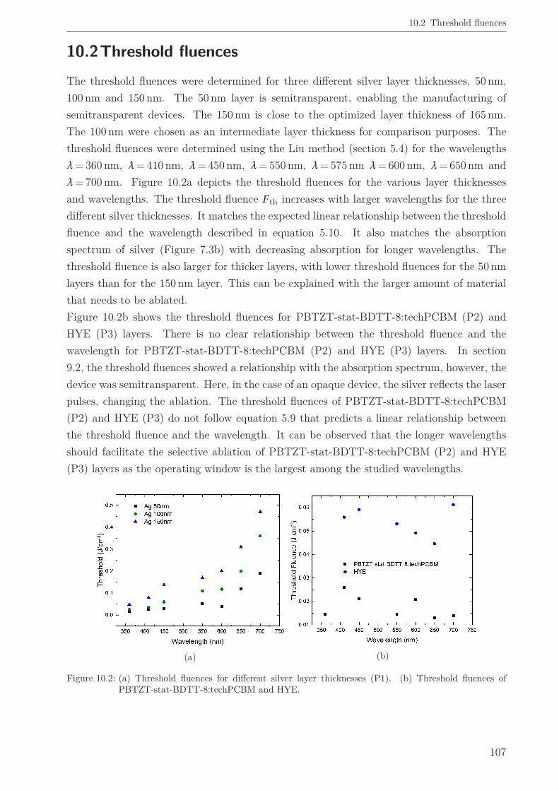
10.2 Threshold fluences
10.2Threshold fluencesThe threshold fluences were determined for three different silver layer thicknesses, 50 nm,100 nm and 150 nm. The 50 nm layer is semitransparent, enabling the manufacturing ofsemitransparent devices. The 150 nm is close to the optimized layer thickness of 165 nm.The 100 nm were chosen as an intermediate layer thickness for comparison purposes. Thethreshold fluences were determined using the Liu method (section 5.4) for the wavelengthsλ= 360 nm, λ= 410 nm, λ= 450 nm, λ= 550 nm, λ= 575 nm λ= 600 nm, λ= 650 nm andλ= 700 nm. Figure 10.2a depicts the threshold fluences for the various layer thicknessesand wavelengths. The threshold fluence F th increases with larger wavelengths for the threedifferent silver thicknesses. It matches the expected linear relationship between the thresholdfluence and the wavelength described in equation 5.10. It also matches the absorptionspectrum of silver (Figure 7.3b) with decreasing absorption for longer wavelengths. Thethreshold fluence is also larger for thicker layers, with lower threshold fluences for the 50 nmlayers than for the 150 nm layer. This can be explained with the larger amount of materialthat needs to be ablated.Figure 10.2b shows the threshold fluences for PBTZT-stat-BDTT-8:techPCBM (P2) andHYE (P3) layers. There is no clear relationship between the threshold fluence and thewavelength for PBTZT-stat-BDTT-8:techPCBM (P2) and HYE (P3) layers. In section9.2, the threshold fluences showed a relationship with the absorption spectrum, however, thedevice was semitransparent. Here, in the case of an opaque device, the silver reflects the laserpulses, changing the ablation. The threshold fluences of PBTZT-stat-BDTT-8:techPCBM(P2) and HYE (P3) do not follow equation 5.9 that predicts a linear relationship betweenthe threshold fluence and the wavelength. It can be observed that the longer wavelengthsshould facilitate the selective ablation of PBTZT-stat-BDTT-8:techPCBM (P2) and HYE(P3) layers as the operating window is the largest among the studied wavelengths.
(a) (b)
Figure 10.2: (a) Threshold fluences for different silver layer thicknesses (P1). (b) Threshold fluences ofPBTZT-stat-BDTT-8:techPCBM and HYE.
107

10 All-solution opaque modules
10.3 Structuring process optimization
10.3.1Silver layer structuring (P1)
The ablation process was optimized for 150 nm thick silver layers which is closest to theoptimum thickness of 165 nm.
Laser structuring at λ=360 nm
The structuring process at λ= 360 nm was studied. A fluence F = 60 mJ cm-2 slightly higherthan the threshold fluence F th = 55 mJ cm-2 was tested. With a pulse overlap lower than95 % clean ablation was not achieved with several spots where the silver was not completelyremoved. The ablation mechanism seems to change to stress ablation with a pulse overlaphigher than 98% as some peeling is observed on the sample. Where the silver was completelyremoved, the silver shows no bulges (Figure 10.3b). However, this is not consistent along thewhole laser-written line and the ablation shows high bulges larger than 1 µm. An example ofthe latter is marked by a red circle in figure 10.3a. The laser-written line width is approximate9 µm.
Laser structuring at λ=450 nm
At λ= 450 nm, a fluence F = 150 mJ cm-2 slightly above the threshold fluenceF th = 140 mJ cm-2 was investigated. The pulse overlap was evaluated from 74 % to 99 %.Although, in all the samples, bulges above 200 nm were found. It should be noticed thatwith higher pulse overlap, the height of the bulges increased. With a pulse overlap of 99 % asimilar peeling effect to the one observed at λ= 360 nm occurred. Figure 10.4 shows the 3Dconfocal image and profile of the laser-written line with a pulse overlap of 74 %. Selective
(a) (b)
Figure 10.3: (a) Optical microscope image and (b) confocal profile of the laser-written lines into silver atλ= 360 nm, F = 60 mJ cm-2 and a pulse overlap of 98%. The peeled silver is encircled in red.On the places where the silver was completely removed the bulges are lower than 20 nm.
108
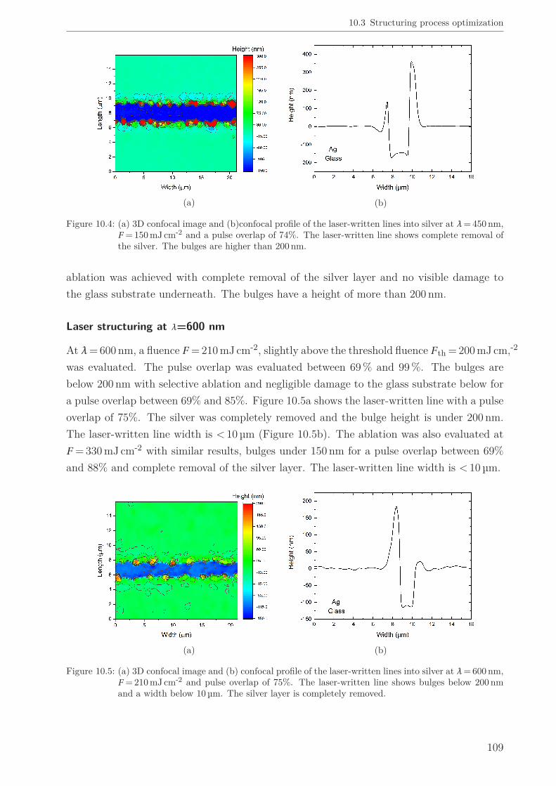
10.3 Structuring process optimization
(a) (b)
Figure 10.4: (a) 3D confocal image and (b)confocal profile of the laser-written lines into silver at λ= 450 nm,F = 150 mJ cm-2 and a pulse overlap of 74%. The laser-written line shows complete removal ofthe silver. The bulges are higher than 200 nm.
ablation was achieved with complete removal of the silver layer and no visible damage tothe glass substrate underneath. The bulges have a height of more than 200 nm.
Laser structuring at λ=600 nm
At λ= 600 nm, a fluence F = 210 mJ cm-2, slightly above the threshold fluence F th = 200 mJ cm,-2
was evaluated. The pulse overlap was evaluated between 69 % and 99 %. The bulges arebelow 200 nm with selective ablation and negligible damage to the glass substrate below fora pulse overlap between 69% and 85%. Figure 10.5a shows the laser-written line with a pulseoverlap of 75%. The silver was completely removed and the bulge height is under 200 nm.The laser-written line width is < 10 µm (Figure 10.5b). The ablation was also evaluated atF = 330 mJ cm-2 with similar results, bulges under 150 nm for a pulse overlap between 69%and 88% and complete removal of the silver layer. The laser-written line width is < 10 µm.
(a) (b)
Figure 10.5: (a) 3D confocal image and (b) confocal profile of the laser-written lines into silver at λ= 600 nm,F = 210 mJ cm-2 and pulse overlap of 75%. The laser-written line shows bulges below 200 nmand a width below 10 µm. The silver layer is completely removed.
109
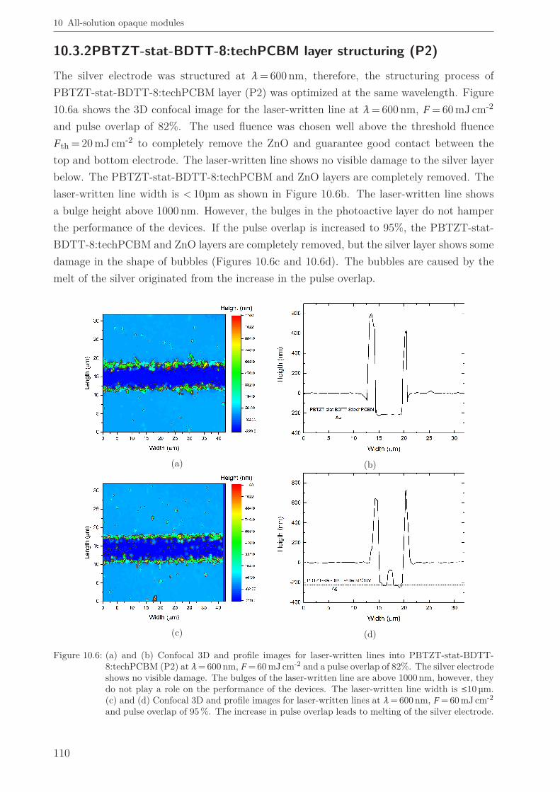
10 All-solution opaque modules
10.3.2PBTZT-stat-BDTT-8:techPCBM layer structuring (P2)
The silver electrode was structured at λ= 600 nm, therefore, the structuring process ofPBTZT-stat-BDTT-8:techPCBM layer (P2) was optimized at the same wavelength. Figure10.6a shows the 3D confocal image for the laser-written line at λ= 600 nm, F = 60 mJ cm-2
and pulse overlap of 82%. The used fluence was chosen well above the threshold fluenceF th = 20 mJ cm-2 to completely remove the ZnO and guarantee good contact between thetop and bottom electrode. The laser-written line shows no visible damage to the silver layerbelow. The PBTZT-stat-BDTT-8:techPCBM and ZnO layers are completely removed. Thelaser-written line width is < 10µm as shown in Figure 10.6b. The laser-written line showsa bulge height above 1000 nm. However, the bulges in the photoactive layer do not hamperthe performance of the devices. If the pulse overlap is increased to 95%, the PBTZT-stat-BDTT-8:techPCBM and ZnO layers are completely removed, but the silver layer shows somedamage in the shape of bubbles (Figures 10.6c and 10.6d). The bubbles are caused by themelt of the silver originated from the increase in the pulse overlap.
(a) (b)
(c) (d)
Figure 10.6: (a) and (b) Confocal 3D and profile images for laser-written lines into PBTZT-stat-BDTT-8:techPCBM (P2) at λ= 600 nm, F = 60 mJ cm-2 and a pulse overlap of 82%. The silver electrodeshows no visible damage. The bulges of the laser-written line are above 1000 nm, however, theydo not play a role on the performance of the devices. The laser-written line width is ≤10 µm.(c) and (d) Confocal 3D and profile images for laser-written lines at λ= 600 nm, F = 60 mJ cm-2
and pulse overlap of 95 %. The increase in pulse overlap leads to melting of the silver electrode.
110

10.3 Structuring process optimization
10.3.3HYE (P3) structuring
The structuring process of HYE (P3) was optimized at λ= 600 nm. Figure 10.7 shows thelaser-written line at λ= 600 nm, with F = 80 mJ cm-2 and pulse overlap of 89 %. The usedfluence is well above the threshold fluence F th = 50 mJ cm-2. The high fluence combined withthe high pulse overlap, guarantee the complete ablation of the HYE layer preventing anyshort on the top electrode. The ablation depth shows the complete removal of the PBTZT-stat-BDTT-8:techPCBM layer together with the HYE (Figure 10.7a). However, this doesnot hamper the performance of the devices. Importantly, the silver layer underneath showsno damage after the ablation. The laser-written line width is < 10µm (Figure 10.7b). Anincrease of the pulse overlap to 97% was also studied. The line shows complete removal of theHYE and PBTZT-stat-BDTT-8:techPCBM layers. The laser-written line width is < 10 µm.Similar to the case of PBTZT-stat-BDTT-8:techPCBM (P2) structuring, the silver layer isdamaged forming bubbles (Figures 10.7c and 10.7d).
(a) (b)
(c) (d)
Figure 10.7: (a) and (b) confocal 3D image and profile for laser-written lines into HYE at λ= 600 nm,F = 80 mJ cm-2 and pulse overlap of 89 %. The PBTZT-stat-BDTT-8:techPCBM layer is re-moved together with the HYE layer. The silver electrode shows no visible damage. The laser-written line width is < 10 µm. (c) and (d) confocal 3D image and profile for laser-written linesat λ= 600 nm, F = 80 mJ cm-2 and pulse overlap of 97 %. The silver bottom electrode showsdamage in the form of melt.
111

10 All-solution opaque modules
Table 10.1: Key performance parameters for the all-solution opaque solar modules.
Device PCE (%) FF (%) Jsc (mA cm-2) Voc (V) GFF (%)
Solar module A 3.7 46 6.0 1.34 95Solar module B 2.6 42 4.9 1.30 99
10.4 Solar module characterizationFirst, solar modules were built using lithography to structure P1 and the laser to structure P2and P3 (Solar module A). Solar module A exhibits a V oc = 1.34 V demonstrating a workingmonolithic connection. It has a total PCE = 3.7% and a F F = 46% considering just thephotoactive area. Koppitz et al. reported F F = 57%.117 The F F reduction may stem fromthe laser structuring outside of the cleanroom environment. Solar modules using the laserto structure P1, P2 and P3 were built as well (Solar module B). Solar module B exhibits aV oc = 1.30 V which is slightly lower than solar module A. The device has a PCE = 2.6% andF F = 42%. The lower F F is caused by the increase in shunts due to the laser structuring ofP1. The short-circuit current density is lower of solar module B is lower J sc = 4.9 mJ cm-2
than the short-circuit current of solar module A Jsc = 6 mJ cm-2. Figure 10.8 shows theJ-V curves of solar modules A and B. The key performance parameters of the devices aresummarized in table 10.1. Both devices have a photoactive area of 1 cm2. Solar module Ahas an inactive area width of 1.05 mm (Figure 10.9a) and a GFF = 95%. Solar module Bhas an inactive area width of 100 µm (Figure 10.9b), leading to a GFF = 99%. Although thedifference in GFF is just 4%, the inactive area in solar module B is 10 times smaller. Thesmall difference in GFF originates from the design of the opaque solar module.
Figure 10.8: J-V curves for the laser structured opaque module. Solar module A, P1 was structured bylithography, P2, P3 were laser structured. Solar module B, P1, P2 and P3 were laser structured.The PCE of Solar Module A is higher.
112

10.5 Discussion
(a) (b)
Figure 10.9: (a) Representative clipping of the inactive area width with P1 structured by lithography and P2,P3 laser structured. (b) Inactive area with P1,P2 and P3 laser structured. The laser structuredinactive area is 10 times smaller.
10.5DiscussionIn this chapter the use of ultra short pulsed lasers to structure opaque all-solution organicsolar modules was demonstrated. Initially the threshold fluences for wavelengths betweenλ= 360 nm and λ= 750 nm were determined. For the silver bottom electrode three differentthicknesses 50 nm, 100 nm and 150 nm were evaluated. The threshold fluence increases withlonger wavelengths for the three different silver layer thicknesses The linear increase of thethreshold fluences with increasing wavelength matches what is stated in equation 5.10. Italso matches the observations in chapter 7 for the evaporated silver as top electrode.The threshold fluences do not have a clear dependence on the wavelength for PBTZT-stat-BDTT-8:techPCBM (P2) and HYE (P3). There is a clear change in the threshold fluenceof the materials when compared to the values reported in section 9.2. The change may beattributed to the presence of the silver electrode that reflects the laser beam and changes theablation conditions. The threshold fluences at different wavelengths do not follow equation5.9 that predicts a linear increase of the threshold fluence with increasing wavelength.On the structuring optimization for the silver (P1) it was demonstrated that, for the struc-turing at λ= 360 nm and λ= 450 nm, the structuring led to high bulges that prevent theconstruction of devices as they will produce shorts. The shorts represent a big challengeto laser structure silver as bottom electrode. The structuring process at λ= 360 nm withhigh pulse overlap showed a peeling of the silver layer. The silver (P1) structuring processwas optimized at λ= 600 nm were the confocal images show peaks below 200 nm, completeremoval of the silver layer and a laser-written line width < 10 µm. The optimum structuringof PBTZT-stat-BDTT-8:techPCBM (P2) and HYE (P3) was also optimized at λ= 600 nm.The process produced clean ablation and no damage to the silver bottom electrode in bothcases. Upon structoring of the HYE top electrodes (P3) the PBTZT-stat-BDTT-8:tech-PCBM was also removed. In both cases, a high pulse overlap damages the silver electrodeforming bubbles.
113

10 All-solution opaque modules
Solar modules were constructed using the optimized laser structuring process at λ= 600 nm.The devices were compared structuring P1 with lithography and with the laser and P2 andP3 with the laser. The devices that were fully structured with the laser presented a slightlylower PCE due to a lower fill factor and short-circuit current densities. However, both devicespresented lower fill factors when compared to the reported by Koppitz et al., possibly causedby exposition to an environment different to the cleanroom where the reported devices weremanufactured. The fully laser structured solar modules exhibit a GFF = 99 % and the solarmodules where P1 was structured by lithographic process exhibit a GFF = 95 %. Althoughthe difference is just 4 % the inactive area for the laser structured devices is 10 times smaller.
114

11 Conclusions and outlook
During this thesis the use of ultrashort pulsed lasers has been investigated for two differenttypes of organic electronic devices, OLEDs and organic solar cells. An ultra fast parametricamplifier was used to explore ablation using different wavelengths. The structuring processis required to connect several devices in series through monolithic connections. This processlimits the area of each individual device, decreasing the ohmic losses. Ultrashort pulsed laserspermit selective ablation and high resolution structures, therefore reducing the inactive areacaused by the monolithic connection.The first step was to investigate the ablation of ITO on top of PET (Chapter 6.1). ITO isone of the most common materials used as electrodes in organic electronics. The thresholdfluences for both materials, ITO and PET, were investigated at different wavelengths betweenλ= 360 nm and λ= 700 nm. A relationship between the threshold fluences and the ITOabsorption was observed were higher absorption led to lower threshold fluence. It seemsto be no relation between the threshold fluence and the absorption spectrum of PET, asthe threshold fluence increases linearly with longer wavelengths. This follows the equationsof Gamaly et al. that calculated a linear relationship between the threshold fluence andthe wavelength.71 Structuring was then explored by overlapping the pulses to write lines.Selective ablation at λ= 360 nm was not possible due to the close threshold fluences for bothITO and PET at this wavelength. Selective ablation was possible at λ= 410 nm, howeverthe bulges were higher than 250 nm. The increase in the pulse overlap led to lower bulges,however at λ= 410 nm this damaged the PET substrates below. At λ= 550 nm selectiveablation with low bulges was achieved. The increase of the pulse overlap was possible dueto the higher working space. At λ= 650 nm and λ= 700 nm the structured lines had evenlower bulges and were selectively ablated. The laser-written lines with high resolution andlow bulges enables the fabrication of mechanically flexible devices.The monolithic connection of OLEDs was then explored (Chapter 7). The threshold fluenceswere investigated for the different materials, ITO, SuperYellow and silver, at five differentwavelengths between λ= 550 nm and λ= 750 nm. The calculated threshold fluences for ITOand SuperYellow remained almost constant through the investigated wavelengths, follow-ing their respective absorption. The silver threshold fluences increase with longer wave-lengths. The absorption of silver may partially explain this, as it decreases with longerwavelengths. However the threshold fluence increases linearly with the wavelength was pre-dicted by Gamaly et al.71 The structuring parameters for P1, P2 and P3 were then foundat λ= 550 nm and λ= 750 nm. In both cases, the laser-written lines fulfill the fabricationrequirements and allowed the construction of operational OLED modules. The OLED mod-
115

11 Conclusions and outlook
ules exhibit twice the onset voltage of the reference devices, showing a working monolithicconnection. They have higher current and power efficiencies demonstrating the advantagesof connecting them in series. Furthermore, the inactive area width was reduced to 45 µm,achieving a GFF = 99.6 %. The small inactive area facilitates the concealment of the mono-lithic connection.The connection of solar cells in series through monolithic connections was then explored.Using an inverted architecture with ZnO as ETL and MoO3 as HTL, and ITO and silveras bottom and top electrode single junction solar modules were built with three differentabsorber layers (PCDTBT:PC71BM, nanoparticulate P3HT:IC60BA and PTB7:PC71BM).The solar modules exhibit comparable performance to the solar cells and in the case ofthe nanoparticulate P3HT:IC60BA the fill factor of the device improved probably due tothe reduced ohmic losses of the solar module. Solar tandem modules were also built, thedevices exhibit a lower performance than the references built under nitrogen atmosphere.The decrease in performance is caused by the water adsorption during the laser processing.Finally, ultrashort pulse lasers were used to experimentally optimize the cell width of thesolar modules. The results were proven by building a 6.5 cm2 solar module composed of 8solar cells. As predicted the device had 87 % of the maximum PCE. All the devices haveinactive area widths in the range of 100 µm, allowing for GFF above 95 %.Ultrashort pulsed laser structuring was tested in semitransparent all-solution modules onflexible PET substrate. PEDOT:PSS in combination with a silver grid was used as bot-tom electrode. PBTZT-stat-BDTT-8:techPCBM was the absorber layer and HYE the topelectrode. The threshold fluences were determined for the wavelengths between λ= 360 nmand λ= 700 nm. A relationship between the absorption spectrum of PEDOT:PSS and thethreshold fluences can be observed as the higher absorption led to reduction in the thresh-old fluences. Similarly, the threshold fluences of PBTZT-stat-BDTT-8:techPCBM and HYEexhibit a relationship with the absorption spectrum. Structured lines were optimized atλ= 600 nm, PEDOT:PSS was structured with little damage to the PET substrate below.The bulge height was under 100 nm. The pulse overlap clearly influences the height of thebulges, as with higher pulse overlap the bulges were reduced. The structured lines wereoptimized for PBTZT-stat-BDTT-8:techPCBM achieving selective ablation with no dam-age to the PEDOT:PSS layer below. The structuring of the HYE layer was done with novisible damage to the PEDOT:PSS layer. Solar modules were then constructed achievingPCE = 3.0 % with a transparency of 20 %. The semitransparent devices are featureless, all-solution processed on flexible devices fulfilling most of the promises of organic solar cells.Finally, the ultrashort pulse laser was explored in opaque all-solution modules on glass. Silverwas used as bottom electrode and PBTZT-stat-BDTT-8:techPCBM was the absorber layerand HYE the top electrode. The threshold fluences were also determined for the wavelengthsbetween λ= 360 nm and λ= 700 nm. Similar to the case were silver was used as top electrode(OLED module), a linear increase with the wavelength is observed, following the work ofGamaly et al. However, this also matches the absorption spectrum of silver. Therefore,further research is necessary to attain a conclusion. Structured lines were optimized at
116

λ= 600 nm. The structured lines on silver exhibit bulges lower than 150 nm with selectiveablation. PBTZT-stat-BDTT-8:techPCBM and HYE were also structured at λ= 600 nmwith no damage to the silver layer below. Solar modules were built with working monolithicconnections as shown by voltage doubling of the devices. However, the solar modules exhibita lower PCE than the ones built by Koppitz et al. using the same architecture.117 The reasonmight be the exposition to an environment different to the cleanroom environment that mighthave contaminated the samples leading to larger shunts. The decrease in fill factor mighthave also been caused by shuts created by peaks on the structured lines on silver that werenot observed during the optimization process. The device exhibit a GFF = 98 %.Although the ablation of P3 produced high bulges in the devices, the performance of theconstructed solar modules was not hampered. However, future investigation should be doneon encapsulated devices. The encapsulation layer may lead to flattening of the bulges leadingto contact on the top electrode and shortened devices. Future manufacturing of OPV needsto investigate this concern.It can be concluded that ultrashort pulse lasers clearly offer several advantages when struc-turing organic electronic devices. Besides enabling the structuring of devices using differentarchitectures as shown in this thesis, ultrashort pulsed lasers are suitable to be integratedon Roll-to-Roll processes. It should be mentioned that ultrashort pulsed lasers are also atechnology that is still being improved. In the near future higher repetitions rates would beavailable allowing the possible printing of devices with higher speeds.The threshold fluence for all the semitransparent thin-film layers showed a dependency withthe absorption. In contrast the silver layers that were investigated showed a linear depen-dency with increasing wavelength. The results in this work could help further theoreticalwork to explain the interaction of femtosecond lasers with thin films at different wavelengths.Further studies can be done in the near infrared of the spectrum where materials like PE-DOT:PSS have absorption bands. This might lead to the selective ablation of PEDOT:PSSon top of the absorber/emitting material possibly reducing the number of failed devices ina future industrial production.Organic electronics have a promising future and ultrashort pulsed lasers facilitate the connec-tion of them for up-scaling purposes with little active area losses. However, organic electron-ics, specially organic solar cells, face other challenges. Crystalline silicon photovoltaic is thedominant technology and it has a clear advantage in terms of PCE and lifetime. Althoughorganic solar cells have some advantages over crystalline silicon like semi-transparency, lowlight performance and mechanical flexibility. Some of these advantages are not present whenorganic solar cells are compared with other technologies like CIGS or amorphous silicon. Arealistic benchmark is required to determine the possible future applications of organic solarcells.OLEDs are already a developed technology for the display market where they are taking anincreasing market share. The use of lasers might help the large area lighting applications asthe structuring lines can be concealed by the light.
117


A Single pulse threshold fluences
In the following tables, a summary of the single pulse threshold fluences of the different materials used in this work is given.
Table A.1: Threshold fluences between λ= 360 nm and λ= 750 nm of some materials used as electrodes in this work.
λ(nm) ITO PET ITO glass PEDOT:PSS HYE-trans. Ag ev. Ag sol. - 50 nm Ag sol. - 100 nm Ag sol. - 150 nm(mJ cm-2) (mJ cm-2) (mJ cm-2) (mJ cm-2) (mJ cm-2) (mJ cm-2) (mJ cm-2) (mJ cm-2)
360 41 - 110 34 - 15 25 48410 169 - 155 33 - 26 35 79450 163 - 120 50 - 30 60 137500 170 - 130 40 - - - -550 169 173 58 36 235 52 110 170600 159 183 61 50 280 40 118 201650 162 172 68 42 333 120 200 310700 160 191 76 64 395 190 360 470750 - 180 - - 490 - - -
119

ASingle
pulsethreshold
fluences
Table A.2: Threshold fluences between λ= 360 nm and λ= 750 nm for some emitter/absorber materials used in this work.
λ(nm) SuperYellow PBTZT-stat-BDTT-8:techPCBM-trans. PBTZT-stat-BDTT-8:techPCBM-opaque(mJ cm-2) (mJ cm-2) (mJ cm-2)
360 - 13 14410 - 20 26450 - 25 21500 - 25 -550 40 30 15600 41 30 20650 45 33 13700 40 60 14750 45 - -
120

fluences for different materials
121


Bibliography
[1] R. Das, K. Ghaffarzadeh, C. Guillaume, and X. He. Printed, Organic & FlexibleElectronics Forecasts, Players & Opportunies 2017-2027.
[2] T. Takatoshi. OLED Display Fundamentals and Applications. John Wiley & Sons,2015.
[3] Daily mail Reporter. UFOs on the M4: Audi reveals bizarre ’swarm’ light that turnsthe back of its cars into a pulsating screen, 2013.
[4] D. Evans. The Internet of Things - How the Next Evolution of the Internet is ChangingEverything. Technical Report April, CISCO, 2011.
[5] IEA. More Data, Less Energy: Making Network Standby More Efficient in Billions ofConnected Devices. Technical report, IEA, 2014.
[6] D. Landerer, D. Bahro, H. Röhm, M. Koppitz, A. Mertens, F. Manger, F. Denk,M. Heidinger, T. Windmann, and A. Colsmann. Solar Glasses: A Case Study onSemitransparent Organic Solar Cells for Self-Powered, Smart, Wearable Devices. En-ergy Technology, 5(11):1936–1945, 2017.
[7] O. Dupré, R. Vaillon, and M. A. Green. Thermal Behavior of Photovoltaic Devices.Springer, 2017.
[8] Deutsche Gesellschaft für Sonnenenergie (DGS). Planning & Installing PhotovoltaicSystems. Earthscan, London, second edition, 2013.
[9] N. Bristow and J. Kettle. Outdoor performance of organic photovoltaics: Diurnal anal-ysis, dependence on temperature, irradiance, and degradation. Journal of Renewableand Sustainable Energy, 7(1):013111, 2015.
[10] M. Nelson. German electricity was nearly 10 times dirtier than France’s in 2016, feb2017.
[11] Coherent. RAPID FX Coherent, 2017.
[12] A. Köhler and H. Bässler. Electronic and Optical Processes of Organic Semiconductors.In Electronic Processes in Organic Semiconductors, pages 193–305. Wiley-VCH VerlagGmbH & Co. KGaA, 2015.
123

BIBLIOGRAPHY
[13] C. Tang. Two-layer organic photovoltaic cell. Applied Physics Letters, 48(2):183–185,1986.
[14] B. Kippelen and J. Brédas. Organic photovoltaics. Energy & Environmental Science,2(3):251, 2009.
[15] M. Eck and M. Krueger. Polymer – Nanocrystal Hybrid Solar Cells. In OrganicPhotovoltaics: Materials, Device Physics, and Manufacturing Technologies. Wiley-VCH Verlag GmbH & Co. KGaA, 2014.
[16] M. C. Scharber, D. Mühlbacher, M. Koppe, P. Denk, C. Waldauf, A. J. Heeger, andC. J. Brabec. Design rules for donors in bulk-heterojunction solar cells - Towards 10% energy-conversion efficiency. Advanced Materials, 18(6):789–794, 2006.
[17] J. Brédas, D. Beljonne, V. Coropceanu, and J. Cornil. Charge-transfer and energy-transfer processes in pi-conjugated oligomers and polymers: a molecular picture.Chemical reviews, 104(11):4971–5004, 2004.
[18] R. Steim, F. R. Kogler, and C. J. Brabec. Interface materials for organic solar cells.Journal of Materials Chemistry, 20(13):2499, 2010.
[19] K. M. O. Malley, H. Yip, and A. K. Jen. Metal Oxide Interlayers for Polymer SolarCells. In Christoph Brabec, Ullrich Scherf, and Vladimir Dyakonov, editors, OrganicPhotovoltaics: Materials, Device Physics, and Manufacturing Technologies, pages 319–341. Wiley-VCH Verlag GmbH & Co. KGaA, 2014.
[20] N. Grossiord, J. M. Kroon, R. Andriessen, and P. W .M. Blom. Degradation mecha-nisms in organic photovoltaic devices. Organic Electronics, 13(3):432–456, 2012.
[21] K. Kawano, R. Pacios, D. Poplavskyy, J. Nelson, D. C. Bradley, and J. R. Durrant.Degradation of organic solar cells due to air exposure. Solar Energy Materials andSolar Cells, 90(20):3520–3530, 2006.
[22] M. P. de Jong, L. J. van IJzendoorn, and M. J. A. de Voigt. Stability of the interface be-tween indium-tin-oxide and poly(3,4-ethylenedioxythiophene)/poly(styrenesulfonate)in polymer light-emitting diodes. Applied Physics Letters, 77(14):2255–2257, 2000.
[23] K. Glaser, A. Pütz, J. Mescher, D. Bahro, and A. Colsmann. Organic Tandem So-lar Cells. In Organic Photovoltaics: Materials, Device Physics, and ManufacturingTechnologies, pages 445–464. Wiley-VCH Verlag GmbH & Co. KGaA, 2014.
[24] D. Bahro, M. Koppitz, A. Mertens, K. Glaser, J. Mescher, and A. Colsmann. Un-derstanding the External Quantum Efficiency of Organic Homo-Tandem Solar CellsUtilizing a Three-Terminal Device Architecture. Advanced Energy Materials, 5(22):1–8, 2015.
124

BIBLIOGRAPHY
[25] A. Hennhöfer. Herstellung effizienter organischer Tandem-Solarmodule. Bachelor the-sis, Karlsruhe Institute of Technology, 2017.
[26] Y. Gao, V. M. Le Corre, A. Gaïtis, M. Neophytou, M. A. Hamid, K. Takanabe, andP. M. Beaujuge. Homo-Tandem Polymer Solar Cells with VOC >1.8 V for EfficientPV-Driven Water Splitting. Advanced Materials, 28(17):3366–3373, 2016.
[27] G. Dennler, M. C. Scharber, T. Ameri, P. Denk, K. Forberich, C. Waldauf, and C. J.Brabec. Design rules for donors in bulk-heterojunction tandem solar cells-towards 15% energy-conversion efficiency. Advanced Materials, 20(3):579–583, 2008.
[28] Press release: Heliatek sets new Organic Photovoltaic world record efficiency of 13.2%,2016.
[29] J. Nelson. The Physics of Solar Cells. Imperial College Press, London, England, 2003.
[30] F. C. Krebs. Polymer solar cell modules prepared using roll-to-roll methods: Knife-over-edge coating, slot-die coating and screen printing. Solar Energy Materials andSolar Cells, 93(4):465–475, 2009.
[31] F. C. Krebs, T. Tromholt, and M. Jørgensen. Upscaling of polymer solar cell fabricationusing full roll-to-roll processing. Nanoscale, 2(6):873, 2010.
[32] M. Powalla, M. Cemernjak, J. Eberhardt, F. Kessler, R. Kniese, H. D. Mohring, andB. Dimmler. Large-area CIGS modules: Pilot line production and new developments.Solar Energy Materials and Solar Cells, 90(18-19):3158–3164, 2006.
[33] P. O. Westin, U. Zimmermann, M. Ruth, and M. Edoff. Next generation interconnec-tive laser patterning of CIGS thin film modules. Solar Energy Materials and SolarCells, 95(4):1062–1068, 2011.
[34] R. R. Arya and D. E. Carlson. Amorphous silicon PV module manufacturing at BPsolar. Progress in Photovoltaics: Research and Applications, 10(2):69–76, 2002.
[35] G. D. Spyropoulos, P. Kubis, N. Li, D. Baran, L. Lucera, M. Salvador, T. Ameri,M. M. Voigt, F. C. Krebs, and C. J. Brabec. Flexible organic tandem solar moduleswith 6% efficiency: combining roll-to-roll compatible processing with high geometricfill factors. Energy Environ. Sci., 7(10):3284–3290, 2014.
[36] S. Röttinger, B. Schwarz, S. Schäfer, R. Gauch, B. Zimmermann, and U. Würfel. Laserpatterning of vacuum processed small molecular weight organic photovoltaics. SolarEnergy Materials and Solar Cells, 154:35–41, 2016.
[37] P. Kubis, L. Lucera, F. Machui, G. Spyropoulos, J. Cordero, A. Frey, J. Kaschta,M. M. Voigt, G. J. Matt, E. Zeira, and C. J. Brabec. High precision processing offlexible P3HT/PCBM modules with geometric fill factor over 95%. Organic Electronics:physics, materials, applications, 15(10):2256–2263, 2014.
125

BIBLIOGRAPHY
[38] Anna Köhler and H Bässler. Index. Electronic Processes in Organic Semiconductors,An Introduction, page 424, 2015.
[39] M. A. Baldo, M. E. Thompson, and S. R. Forrest. Phosphorescent materials forapplication to organic light emitting devices. Pure and Applied Chemistry, 71(11):2095–2106, 1999.
[40] E. F. Schubert. Light-Emitting Diodes. Cambridge University Press, Cambridge,United Kingdom, 2 edition edition, 2006.
[41] Unit of luminous intensity (candela).
[42] K. Neyts, M. Marescaux, A. U. Nieto, A. Elschner, W. Lövenich, K. Fehse, Qi. Huang,K. Walzer, and K. Leo. Inhomogeneous luminance in organic light emitting diodesrelated to electrode resistivity. Journal of Applied Physics, 100(11), 2006.
[43] M. G. Kang and L Jay Guo. Nanoimprinted Semitransparent Metal Electrodesand Their Application in Organic Light-Emitting Diodes. Advanced Materials,19(10):1391–1396, 2007.
[44] M. Slawinski, M. Weingarten, M. Heuken, a. Vescan, and H. Kalisch. Investigation oflarge-area OLED devices with various grid geometries. Organic Electronics: physics,materials, applications, 14(10):2387–2391, 2013.
[45] J. Park, J. Lee, D. Shin, and S. Park. Luminance uniformity of large-area OLEDs withan auxiliary metal electrode. IEEE/OSA Journal of Display Technology, 5(8):306–311,2009.
[46] C. Chang, J. Chen, S. Hwang, and C. H. Chen. Highly efficient white organicelectroluminescent devices based on tandem architecture. Applied Physics Letters,87(25):253501, 2005.
[47] C. W. Chen, Y. J. Lu, C. C. Wu, E. H. E. Wu, C. W. Chu, and Y. Yang. Effectiveconnecting architecture for tandem organic light-emitting devices. Applied PhysicsLetters, 87(24):1–3, 2005.
[48] T. Lee, T. Noh, B. Choi, M. Kim, D. W. Shin, and J. Kido. High-efficiency stackedwhite organic light-emitting diodes. Applied Physics Letters, 92(4):043301, 2008.
[49] H. Sasabe and J. Kido. Development of high performance OLEDs for general lighting.Journal of Materials Chemistry C, 1:1699, 2013.
[50] S. Höfle, A. Schienle, C. Bernhard, M. Bruns, U. Lemmer, and A. Colsmann. Solutionprocessed, white emitting tandem organic light-emitting diodes with inverted devicearchitecture. Advanced Materials, 26(30):5155–5159, 2014.
126

BIBLIOGRAPHY
[51] K. S. Yook, S. O. Jeon, S. Y. Min, J. Y. Lee, H. J. Yang, T. Noh, S. K. Kang, andT. W. Lee. Highly efficient p-i-n and tandem organic light-emitting devices usingan air-stable and low-temperature-evaporable metal azide as an n-dopant. AdvancedFunctional Materials, 20(11):1797–1802, 2010.
[52] A. R. Duggal, D. F. Foust, W. F. Nealon, and C. M. Heller. Fault-tolerant, scalableorganic light-emitting device architecture. Applied Physics Letters, 82(16):2580–2582,2003.
[53] F. C. Krebs. Fabrication and processing of polymer solar cells: A review of printingand coating techniques. Solar Energy Materials and Solar Cells, 93(4):394–412, 2009.
[54] F. Völz. Herstellung und Charakterisierung organischer Mini-Solarmodule. Bachelorthesis, Karlsruhe Institute of Technology, 2014.
[55] L. D. Landau and V. G. Levich. Dragging of a liquid by a moving plate. ActaPhysicochimica U.R.S.S., 17:42–54, 1942.
[56] Rolf Theodor Borlinghaus. Confocal Microscopy. In The White Confocal, pages 47–66.Springer, 2017.
[57] M. Hochberg. Optoelectronic and surface properties of BODIPY solar cells (MScThesis). PhD thesis, Karlsruhe Institute of Technology, 2014.
[58] T. Leonhard. Charakterisierung von Blei-Perowskitschichten mittels Rasterkraft-mikroskopie. Master thesis, Karlsruhe Institute of Technology, 2016.
[59] Operator’s manual Libra Ultrafast Amplifier Laser System.
[60] F. Träger. Springer Handbook of lasers and optics. Springer, Kassel, Germany, 2007.
[61] M. Eichhorn. Laser Physics. Springer, Cambridge, United Kingdom, 2014.
[62] K. F. Renk. Basics of Laser Physics, Graduate Texts in Physics. Springer, secondedition, 2012.
[63] W. Koechner. 8. Q-Switching. In Solid-State Laser Engineering, chapter 8. Q-Switc,pages 488–533. Springer, Round Hill, U.S.A., sixth edit edition, 2006.
[64] K. F. Renk. Basics of Laser Physics, Graduate Texts in Physics. Springer, Regensburg,Germany, second edition, 2012.
[65] W. Koechner. 9 . Mode Locking. In Solid-State Laser Engineering, pages 534–586.Springer, Round Hill, U.S.A., 6th edition, 2006.
[66] R. W. Boyd. Nonlinear optics. Elsevier, third edit edition, 2010.
127

BIBLIOGRAPHY
[67] D. Bäuerle. Laser Processing and Chemistry. Springer, Linz, Austria, fourth ediedition, 2011.
[68] H. Hügel and T. Graf. Laser in der Fertigung. Vieweg+Teubner, Stuttgart, Germany,2nd editio edition, 2009.
[69] B. Neuenschwander, B. Jaeggi, M. Schmid, A. Dommann, A. Neels, T. Bandi, andGuido Hennig. Factors controlling the incubation in the application of ps laser pulseson copper and iron surfaces. Laser Applications in Microelectronic and OptoelectronicManufacturing (LAMOM) XVIII, 8607:86070D, 2013.
[70] K. Sugioka, M. Michael, and A. Piqué. Laser Precision Microfabrication. Springer,Saitama, Japan, first edit edition, 2010.
[71] E. G. Gamaly, A. V. Rode, B. Luther-Davies, and V. T. Tikhonchuk. Ablation ofsolids by femtosecond lasers: Ablation mechanism and ablation thresholds for metalsand dielectrics. Physics of Plasmas, 9(3):949, 2002.
[72] M. J. Liu. Simple technique for measurements of pulsed Gaussian-beam spot sizes.Opt. Lett., 7(5):196–198, 1982.
[73] A. Ben-Yakar and R. L. Byer. Femtosecond laser ablation properties of borosilicateglass. Journal of Applied Physics, 96(9):5316–5323, 2004.
[74] T. L. Breen, P. M. Fryer, R. W. Nunes, and M. E. Rothwell. Patterning Indium TinOxide and Indium Zinc Oxide Using Microcontact Printing and Wet Etching. Society,18(24):194–197, 2002.
[75] O. Ourida, B. M. Said, T. Thierry, and S. Martin. ITO Etched by PhotolithographyUsed in the Fabrication of Flexible Organic Solar Cells with PET Substrates. Journalof Energy and Power Engineering, 8:107–111, 2014.
[76] H. W. Choi, Dave F. Farson, J. Bovatsek, A. Arai, and D. Ashkenasi. Direct-writepatterning of indium-tin-oxide film by high pulse repetition frequency femtosecondlaser ablation. Applied optics, 46(23):5792–5799, 2007.
[77] G. Raciukaitis, M. Brikas, M. Gedvilas, and T. Rakickas. Patterning of indium-tinoxide on glass with picosecond lasers. Applied Surface Science, 253(15):6570–6574,2007.
[78] S. Krause, P. T. Miclea, S. Schweizer, and G. Seifert. Optimized scribing of TCOlayers on glass by selective femtosecond laser ablation. Conference Record of the IEEEPhotovoltaic Specialists Conference, 40601:2432–2435, 2013.
[79] H. Tsai, H. Yang, C. Pan, and M. Chou. Laser Patterning Indium Tin Oxide ( ITO )Coated on PET Substrate. SPIE proceedings, 4230:156–163, 2000.
128

BIBLIOGRAPHY
[80] C. McDonnell, D. Milne, C. Prieto, H. Chan, D. Rostohar, and G. M. O’Connor. Laserpatterning of very thin indium tin oxide thin films on PET substrates. Applied SurfaceScience, 359:567–575, 2015.
[81] O. Ghandour. Excimer ablation of ITO on flexible substrates for large format displayapplications. Proceedings of SPIE, 4637:90–101, 2002.
[82] S. Xiao, S. A. Fernandes, and A. Ostendorf. Selective patterning of ITO on flexiblePET Substrate by 1064nm picosecond Laser. Physics Procedia, 12(PART 2):125–132,2011.
[83] K. Hirschfelder, M. Schaefer, and A. Gillner. Ultrashort-pulsed laser processing andsolution based coating in roll- to-roll manufacturing of organic photovoltaics. SPIEproceedings, 9567:1–7, 2015.
[84] Kr. Neyts, A. Real, M. Marescaux, S. Mladenovski, and J. Beeckman. Conductor gridoptimization for luminance loss reduction in organic light emitting diodes. Journal ofApplied Physics, 103(9), 2008.
[85] S. Harkema, S. Mennema, M. Barink, H. Rooms, Joanne S. Wilson, Ton van Mol, andDirk Bollen. Large area ITO-free flexible white OLEDs with Orgacon PEDOT:PSSand printed metal shunting lines. Proceedings of SPIE, 7415(0):74150T–74150T–8,2009.
[86] J. Park, J. Lee, and Y. Y. Noh. Optical and thermal properties of large-area OLEDlightings with metallic grids. Organic Electronics: physics, materials, applications,13(1):184–194, 2012.
[87] J. Fragoso, S. Höfle, M. Zhang, J. Dlugosch, T. Friedrich, S. Wagner, and A. Colsmann.OLED Luminaires: Device Arrays with 99.6% Geometric Fill Factor Structured byFemtosecond Laser Ablation. ACS Applied Materials and Interfaces, 9(43):37898–37904, 2017.
[88] H. J. Bolink, E. Coronado, J. Orozco, and M. Sessolo. Efficient polymer light-emittingdiode using air-stable metal oxides as electrodes. Advanced Materials, 21(1):79–82,2009.
[89] H. J. Bolink, E. Coronado, D. Repetto, and M. Sessolo. Air stable hybrid organic-inorganic light emitting diodes using ZnO as the cathode. Applied Physics Letters,91(22):2005–2008, 2007.
[90] S. Höfle, A. Schienle, M. Bruns, U. Lemmer, and A. Colsmann. Enhanced electroninjection into inverted polymer light-emitting diodes by combined solution-processedzinc oxide/polyethylenimine interlayers. Advanced Materials, 26(17):2750–2754, 2014.
129
BIBLIOGRAPHY
[91] Yi. Zhou, C. Fuentes-hernandez, J. Shim, J. Meyer, A. J. Giordano, H. Li, P. Winget,T. Papadopoulos, H. Cheun, J. Kim, M. Fenoll, A. Dindar, W. Haske, E. Najafabadi,T. M. Khan, H. Sojoudi, S. Barlow, S. Graham, J. Brédas, S. R. Marder, A. Kahn,and B. Kippelen. for Organic Electronics. Science, 873(April):327–332, 2012.
[92] M. Zhang. Fully Solution Processed Transparent Organic Light Emitting Diodes. Masterthesis, Karlsruhe Institute of Technology, 2013.
[93] H. You, Y. Dai, Z. Zhang, and D. Ma. Improved performances of organic light-emittingdiodes with metal oxide as anode buffer. Journal of Applied Physics, 101(2):2005–2008,2007.
[94] L. Lucera, F. Machui, P. Kubis, H. D. Schmidt, J. Adams, S. Strohm, T. Ahmad,K. Forberich, H.-J. Egelhaaf, and C. J. Brabec. Highly efficient, large area, roll coatedflexible and rigid OPV modules with geometric fill factors up to 98.5% processed withcommercially available materials. Energy Environ. Sci., 9(1):89–94, 2016.
[95] M. Seeland and H. Hoppe. Comparison of distributed vs. lumped series resistancemodeling of thin-film solar cells and modules: Influence on the geometry-dependentefficiency. Phys. Status Solidi A, 212(9):1991–2000, 2015.
[96] N. Blouin, A. Michaud, and M. Leclerc. A low-bandgap poly(2,7-carbazole) derivativefor use in high-performance solar cells. Advanced Materials, 19(17):2295–2300, 2007.
[97] S. Beaupré and M. Leclerc. PCDTBT: en route for low cost plastic solar cells. Journalof Materials Chemistry A, 1:11097–11105, 2013.
[98] C. H. Peters, I. T. Sachs-Q., J. P. Kastrop, S. Beaupré, M. Leclerc, and M. D. McGehee.High efficiency polymer solar cells with long operating lifetimes. Advanced EnergyMaterials, 1(4):491–494, 2011.
[99] A. T. Kleinschmidt, S.E. Root, and D. J. Lipomi. Poly(3-hexylthiophene) (P3HT):fruit fly or outlier in organic solar cell research? J. Mater. Chem. A, 10(c):93–116,2017.
[100] G. J. Zhao, Y. J. He, and Y. Li. 6.5% efficiency of polymer solar cells based onpoly(3-hexylthiophene) and indene-C60 bisadduct by device optimization. AdvancedMaterials, 22(39):4355–4358, 2010.
[101] Ji. Hou, H. H. Chen, S. Zhang, R. I. Chen, Y. Yang, Y. Wu, and G. Li. Synthesisof a low band gap polymer and its application in highly efficient polymer solar cells.Journal of the American Chemical Society, 131(43):15586–15587, 2009.
[102] Z. He, C. Zhong, S. Su, M. Xu, H. Wu, and Y. Cao. Enhanced Power-ConversionEfficiency in Polymer Solar Cells Using an Inverted Device Structure Enhanced power-conversion efficiency in polymer solar cells using an inverted device structure. NaturePhotonics, 6(9):591–595, 2012.
130
BIBLIOGRAPHY
[103] M. M. Wienk, J. M. Kroon, W. J. H. Verhees, J. Knol, J. C. Hummelen, P. A. van Hal,and R. A. J. Janssen. Efficient Methano[70]fullerene/MDMO-PPV Bulk Heterojunc-tion Photovoltaic Cells. Angewandte Chemie International Edition, 42(29):3371–3375,2003.
[104] H. Youjun, C. Hsiang-Yu, H. Jianhui, and L. Yongfang. 2010_Indene−C60 Bisadduct- A New Acceptor for High-Performance Polymer Solar Cells_KW.pdf. Journal of theAmerican Chemical Society, 132(4):1377–1382, 2010.
[105] K. Mazzio and C. K. Luscombe. The future of organic photovoltaics. Chem. Soc. Rev.,44(1):78–90, 2014.
[106] A. Elschner, S. Kirchmeyer, W. Lovenich, W. Merker, and R. Knud. PEDOT: Princi-ples and Applications of an Intrinsically Conductive Polymer. CRC Press, 2010.
[107] A. M. Nardes, M. Kemerink, M. M. de Kok, E. Vinken, K. Maturova, and R. A JJanssen. Conductivity, work function, and environmental stability of PEDOT:PSSthin films treated with sorbitol. Organic Electronics: physics, materials, applications,9(5):727–734, 2008.
[108] S. Gärtner, M. Christmann, S. Sankaran, H. Röhm, E. M. Prinz, F. Penth, A. Pütz,A. E. Türeli, B. Penth, B. Baumstümmler, and A. Colsmann. Eco-friendly fabrica-tion of 4% efficient organic solar cells from surfactant-free P3HT:ICBA nanoparticledispersions. Advanced Materials, pages 6653–6657, 2014.
[109] S. Sankaran, K. Glaser, S. Gärtner, T. Rödlmeier, K. Sudau, G. Hernandez-Sosa, andA. Colsmann. Fabrication of polymer solar cells from organic nanoparticle disper-sions by doctor blading or ink-jet printing. Organic Electronics: physics, materials,applications, 28:118–122, 2016.
[110] J. Chung, S. Han, D. Lee, S. Ahn, C. P. Grigoropoulos, J. Moon, and S. H.Ko. Nanosecond laser ablation of silver nanoparticle film. Optical Engineering,52(2):021010–1, 2013.
[111] D. Huang, Y. Li, Z. Xu, S. Zhao, L. Zhao, and J. Zhao. Enhanced performance and mor-phological evolution of PTB7:PC71BM polymer solar cells by using solvent mixtureswith different additives. Physical chemistry chemical physics : PCCP, 17(12):8053–60,2015.
[112] K. Kawano, R. Pacios, D. Poplavskyy, J. Nelson, D. C Bradley, and J. R. Durrant.Degradation of organic solar cells due to air exposure. Solar Energy Materials andSolar Cells, 90(20):3520–3530, 2006.
[113] K. Glaser. Hochskalierung und Defektcharakterisierung von organische Solarzellen.Phd thesis, Karlsruhe Institute of Technology, 2017.
131

BIBLIOGRAPHY
[114] F. Guo, N. Li, V. V. Radmilović, V. R. Radmilović, M. Turbiez, Er. Spiecker, K. For-berich, and C. J. Brabec. Fully printed organic tandem solar cells using solution-processed silver nanowires and opaque silver as charge collecting electrodes. EnergyEnviron. Sci., 8(6):1690–1697, 2015.
[115] J. Krantz, K. Forberich, P. Kubis, F. Machui, J. Min, T. Stubhan, and C. J. Brabec.Printing high performance reflective electrodes for organic solar cells. Organic Elec-tronics, 17:334–339, 2015.
[116] F. Nickel, T. Haas, E. Wegner, D. Bahro, S. Salehin, O. Kraft, P. A. Gruber, andA. Colsmann. Mechanically robust, ITO-free, 4.8% efficient, all-solution processed or-ganic solar cells on flexible PET foil. Solar Energy Materials and Solar Cells, 130:317–321, 2014.
[117] M. Koppitz, N. Hesse, D. Landerer, L. GrafvonReventlow, E. Wegner, J. Czolk, andA. Colsmann. Organic Solar Modules: Fully Doctor Bladed on Glass in Air. EnergyTechnology, pages 1105–1111, 2017.
[118] C. Chen, L. Dou, J. Gao, W. Chang, G. Li, and Y. Yang. High-performance semi-transparent polymer solar cells possessing tandem structures. Energy & EnvironmentalScience, 6(9):2714–2720, 2013.
[119] M. Song, D. S. You, K. Lim, S. Park, S. Jung, C. S. Kim, D. H. Kim, D. G. Kim,Jo. K. Kim, J. Park, Y. C. Kang, J. Heo, S. H. Jin, J. H. Park, and J. W. Kang.Highly efficient and bendable organic solar cells with solution-processed silver nanowireelectrodes. Advanced Functional Materials, 23(34):4177–4184, 2013.
[120] F. Guo, Xi. Zhu, K. Forberich, J. Krantz, T. Stubhan, M. Salinas, M. Halik, S. Spallek,B. Butz, E. Spiecker, T. Ameri, N. Li, P. Kubis, D. M. Guldi, G. J. Matt, and C. J.Brabec. ITO-free and fully solution-processed semitransparent organic solar cells withhigh fill factors. Advanced Energy Materials, 3(8):1062–1067, 2013.
[121] J. H. Yim, S. Y. Joe, C. Pang, K. M. Lee, H. Jeong, J.Y. Park, Y. H. Ahn, J. C. DeMello, and S. Lee. Fully solution-processed semitransparent organic solar cells with asilver nanowire cathode and a conducting polymer anode. ACS Nano, 8(3):2857–2863,2014.
[122] F. Guo, P. Kubis, T. Stubhan, N. Li, D. Baran, T. Przybilla, E. Spiecker, K. Forberich,and C. J. Brabec. Fully solution-processing route toward highly transparent polymersolar cells. ACS Applied Materials and Interfaces, 6(20):18251–18257, 2014.
[123] Y. Xia, K. Sun, and J. Ouyang. Solution-processed metallic conducting polymer filmsas transparent electrode of optoelectronic devices. Advanced Materials, 24(18):2436–2440, 2012.
132

BIBLIOGRAPHY
[124] M. Zhang, S. Höfle, J. Czolk, A. Mertens, and A. Colsmann. All-solution processedtransparent organic light emitting diodes. Nanoscale, 7:20009–20014, 2015.
[125] M. Song, H. Kim, C. S. Kim, J. Jeong, C. Cho, J. Lee, S. Jin, D. Choi, and D. Kim.ITO-free highly bendable and efficient organic solar cells with Ag nanomesh/ZnOhybrid electrodes. J. Mater. Chem. A, 3(1):65–70, 2014.
[126] M. Reinhard, R. Eckstein, A. Slobodskyy, U. Lemmer, and A. Colsmann. Solution-processed polymer – silver nanowire top electrodes for inverted semi-transparent solarcells. Organic Electronics, 14(1):273–277, 2013.
[127] M. Helgesen, J. E. Carlé, and F. C. Krebs. Slot-die coating of a high performancecopolymer in a readily scalable roll process for polymer solar cells. Advanced EnergyMaterials, 3(12):1664–1669, 2013.
[128] M. Hösel, R. R. Søndergaard, M. Jørgensen, and F. C. Krebs. Fast Inline Roll-to-RollPrinting for Indium-Tin-Oxide-Free Polymer Solar Cells Using Automatic Registration.Energy Technology, 1(1):102–107, 2013.
[129] B. Muhsin, R. Roesch, G. Gobsch, and H. Hoppe. Flexible ITO-free polymer solarcells based on highly conductive PEDOT:PSS and a printed silver grid. Solar EnergyMaterials and Solar Cells, 130:551–554, 2014.
[130] I. Burgués-Ceballos, N. Kehagias, C. M. Sotomayor-Torres, M. Campoy-Quiles, andP. D. Lacharmoise. Embedded inkjet printed silver grids for ITO-free organic solarcells with high fill factor. Solar Energy Materials and Solar Cells, 127:50–57, 2014.
[131] T. M. Eggenhuisen, Y. Galagan, a. F. K. V. Biezemans, T. M. W. L. Slaats, W. P.Voorthuijzen, S. Kommeren, S. Shanmugam, J. P. Teunissen, A. Hadipour, W. J. H.Verhees, S. C. Veenstra, M. J. J. Coenen, J. Gilot, R. Andriessen, and W. a. Groen.High efficiency, fully inkjet printed organic solar cells with freedom of design. J. Mater.Chem. A, 3(14):7255–7262, 2015.
[132] J. Czolk, D. Landerer, M. Koppitz, D. Nass, and A. Colsmann. Highly Efficient,Mechanically Flexible, Semi-Transparent Organic Solar Cells Doctor Bladed from Non-Halogenated Solvents. Advanced Materials Technologies, 1(9):1600184, 2016.
[133] S. Berny, N. Blouin, A. Distler, H. J. Egelhaaf, M. Krompiec, A. Lohr, O. R. Lozman,G. E. Morse, L. Nanson, A. Pron, T. Sauermann, N. Seidler, S. Tierney, P. Tiwana,M. Wagner, and H. Wilson. Solar trees: First large-scale demonstration of fully solutioncoated, semitransparent, flexible organic photovoltaic modules. Advanced Science,3(5):1–7, 2015.
[134] B. Knight, J. Hummelen, F. LePeq, and F. Wudl. Preparation and Characterizationof Fulleroid and Methanofullerene Derivatives. J. Org. Chem, 60(21):532–538, 1995.
133

BIBLIOGRAPHY
[135] N. G. Semaltianos, C. Koidis, C. Pitsalidis, P. Karagiannidis, S. Logothetidis, W. Per-rie, D. Liu, S. P. Edwardson, E. Fearon, R. J. Potter, G. Dearden, and K. G. Watkins.Picosecond laser patterning of PEDOT:PSS thin films. Synthetic Metals, 161(5-6):431–439, 2011.
[136] A. Schoonderbeek. Laser Processing of Thin Films for Photovoltaic Applications.Journal of Laser Micro/Nanoengineering, 5(3):248–255, 2010.
[137] F. Guo, P. Kubis, T. Przybilla, Er. Spiecker, A. Hollmann, S. Langner, K. Forberich,and C. J. Brabec. Nanowire Interconnects for Printed Large-Area SemitransparentOrganic Photovoltaic Modules. Advanced Energy Materials, 5(12):1401779, 2015.
[138] N. Bellini, R. Geremia, and D. Karnakis. Increasing laser pulse overlap restricts pi-cosecond laser ablation of thin metal films near ablation threshold. Applied Physics A:Materials Science and Processing, 123(5):1–6, 2017.
134

List of Figures
1.1 First device with an OLED display. . . . . . . . . . . . . . . . . . . . . . . . . . . . 11.2 OPV solar glasses. . . . . . . . . . . . . . . . . . . . . . . . . . . . . . . . . . . . . . 2
2.1 s and p orbitals in a carbon atom together with the ethene molecule. . . . . . . . 52.2 Energy level diagram for ethene. . . . . . . . . . . . . . . . . . . . . . . . . . . . . . 62.3 Hopping process in organic electronics. . . . . . . . . . . . . . . . . . . . . . . . . . 72.4 Bilayer heterojunction and bulk heterojunction solar cell. . . . . . . . . . . . . . . 82.5 Photovoltaic process in an organic solar cell. . . . . . . . . . . . . . . . . . . . . . 92.6 Regular and inverted architectures for organic solar cells. . . . . . . . . . . . . . . 102.7 Ohmic contact definition. . . . . . . . . . . . . . . . . . . . . . . . . . . . . . . . . . 112.8 Absorption spectrum coverage for homo and hetero tandem solar cells. . . . . . . 122.9 Equivalent circuit of a solar cell. . . . . . . . . . . . . . . . . . . . . . . . . . . . . . 132.10 Current density - voltage graph of a solar cell. . . . . . . . . . . . . . . . . . . . . . 142.11 Monolithically connected solar cells. . . . . . . . . . . . . . . . . . . . . . . . . . . . 152.12 OLED working principle. . . . . . . . . . . . . . . . . . . . . . . . . . . . . . . . . . 162.13 Vectorial representation of the four different spin configurations. . . . . . . . . . . 17
3.1 Doctor blading system. . . . . . . . . . . . . . . . . . . . . . . . . . . . . . . . . . . 223.2 Confocal microscope working principle. . . . . . . . . . . . . . . . . . . . . . . . . . 243.3 AFM tapping mode working principle. . . . . . . . . . . . . . . . . . . . . . . . . . 253.4 Libra optical bench assembly. . . . . . . . . . . . . . . . . . . . . . . . . . . . . . . 273.5 Simplified schematic OPerA Solo. . . . . . . . . . . . . . . . . . . . . . . . . . . . . 303.6 OPerA Solo pulse energies for different wavelengths. . . . . . . . . . . . . . . . . . 303.7 µFAB schematic. . . . . . . . . . . . . . . . . . . . . . . . . . . . . . . . . . . . . . . 31
4.1 Schematic laser oscillator. . . . . . . . . . . . . . . . . . . . . . . . . . . . . . . . . . 334.2 Light interactions with a two level system. . . . . . . . . . . . . . . . . . . . . . . . 344.3 Four-level laser system and the light interactions within. . . . . . . . . . . . . . . 364.4 Energy levels in a Ti:Sapphire laser. . . . . . . . . . . . . . . . . . . . . . . . . . . 374.5 Q-switching process. . . . . . . . . . . . . . . . . . . . . . . . . . . . . . . . . . . . . 384.6 Chirp amplification process using two Pockels cells. . . . . . . . . . . . . . . . . . 394.7 Frequency relationship in a parametric amplification. . . . . . . . . . . . . . . . . 404.8 Frequency relationship in a sum-frequency interaction. . . . . . . . . . . . . . . . 41
5.1 Overview of different laser interactions depending on the intensity. . . . . . . . . 43
135
LIST OF FIGURES
5.2 Temperature and ablation velocity schematic of a surface hit by a laser source. . 465.3 Interaction times of femtosecond pulses with dielectric and metals. . . . . . . . . 47
6.1 Threshold fluences and absorption spectrum for ITO and PET. . . . . . . . . . . 526.2 ITO on PET ablation at λ= 360 nm. . . . . . . . . . . . . . . . . . . . . . . . . . . 536.3 Line structuring on ITO at λ= 410 nm. . . . . . . . . . . . . . . . . . . . . . . . . . 546.4 Line structuring on ITO at λ= 550 nm. . . . . . . . . . . . . . . . . . . . . . . . . . 556.5 Line structuring on ITO at λ= 650 nm. . . . . . . . . . . . . . . . . . . . . . . . . . 566.6 Line structuring on ITO at λ= 700 nm. . . . . . . . . . . . . . . . . . . . . . . . . . 576.7 SEM image of the laser-written line at λ= 700 nm. . . . . . . . . . . . . . . . . . . 58
7.1 SuperYellow emission and molecular structure. . . . . . . . . . . . . . . . . . . . . 627.2 OLED module architecture and sample design. . . . . . . . . . . . . . . . . . . . . 637.3 Threshold fluences and absorption spectra for the OLED module layers. . . . . . 647.4 ITO structuring (P1) at λ= 550 nm and λ= 750 nm. . . . . . . . . . . . . . . . . . 657.5 ZnO/PEI/SuperYellow structuring (P2). . . . . . . . . . . . . . . . . . . . . . . . . 667.6 MoO3/silver (P3) structuring. . . . . . . . . . . . . . . . . . . . . . . . . . . . . . . 677.7 Monolithic connection and shining OLED module. . . . . . . . . . . . . . . . . . . 687.8 JVL curves, luminance vs current density and current efficiency. . . . . . . . . . . 69
8.1 Molecular structure of the polymer electron donors used in this work. . . . . . . 748.2 Molecular structure of two fullerenes used as electron acceptors in this work. . . 768.3 Single-junction solar module architecture and 16 x 16 mm2 design. . . . . . . . . . 768.4 PCDTBT:PC71BM (P2) structuring characterization. . . . . . . . . . . . . . . . . 788.5 J-V curves of the solar cell and module using PCDTBT:PC71BM. . . . . . . . . . 798.6 Single-junction solar module architecture and 25 x 25 mm2 design. . . . . . . . . . 808.7 Nanoparticulate P3HT:IC60BA structuring characterization. . . . . . . . . . . . . 818.8 J-V curves for the best solar module and reference solar cell using P3HT:ICBA. 828.9 Architectures for the single-junction and tandem solar modules. . . . . . . . . . . 838.10 PTB7:PC71BM single-junction and tandem layers structuring characterization. . 848.11 J-V curves for the single, tandem solar cells and modules. . . . . . . . . . . . . . 858.12 Substrate design for the solar cell width optimization. . . . . . . . . . . . . . . . . 868.13 Key performance parameters for the single-junction and tandem devices. . . . . 878.14 Effort vs PCE graph and 8 cell solar module. . . . . . . . . . . . . . . . . . . . . . 88
9.1 Silver grid optical microscope image and transmission. SEM image and trans-mission/resistance of HYE. . . . . . . . . . . . . . . . . . . . . . . . . . . . . . . . . 92
9.2 Semi-transparent solar module architecture. . . . . . . . . . . . . . . . . . . . . . . 939.3 Threshold fluences and absorption spectra for semi-transparent device. . . . . . . 949.4 Single pulse ablation of PEDOT:PSS on top of PET at λ= 360 nm. . . . . . . . . 969.5 Laser-written line on PEDOT:PSS (P1) at λ= 450 nm. . . . . . . . . . . . . . . . 979.6 Laser-written line into PEDOT:PSS (P1) at λ= 600 nm. . . . . . . . . . . . . . . 98
136

LIST OF FIGURES
9.7 Laser-written line into PBTZT-stat-BDTT-8:techPCBM at λ= 600 nm. . . . . . 999.8 Ablation process int HYE with different pulse overlaps at λ= 600 nm. . . . . . . 1009.9 J-V curves and monolithic connection of the semi-transparent solar module. . . . 1019.10 P1, P2 and P3 structuring steps on the semi-transparent solar module. . . . . . . 103
10.1 Architecture and solar module design of the all-solution opaque solar modules. . 10610.2 Threshold fluences opaque solar module layers. . . . . . . . . . . . . . . . . . . . . 10710.3 Laser-written lines on silver at λ= 360 nm. . . . . . . . . . . . . . . . . . . . . . . 10810.4 Laser-written lines on silver at λ= 450 nm. . . . . . . . . . . . . . . . . . . . . . . 10910.5 Laser-written lines on silver at λ= 600 nm. . . . . . . . . . . . . . . . . . . . . . . 10910.6 Laser-written lines into PBTZT-stat-BDTT-8:techPCBM at λ= 600 nm. . . . . . 11010.7 Laser-written lines on HYE at λ= 600 nm. . . . . . . . . . . . . . . . . . . . . . . . 11110.8 J-V curves for the laser structured opaque solar module. . . . . . . . . . . . . . . 11210.9 Inactive area width for opaque module. . . . . . . . . . . . . . . . . . . . . . . . . . 113
137


List of Tables
3.1 Libra output beam characteristics . . . . . . . . . . . . . . . . . . . . . . . . . . . . 283.2 OPerA Solo wavelength regimes. . . . . . . . . . . . . . . . . . . . . . . . . . . . . . 293.3 Objectives specifications. . . . . . . . . . . . . . . . . . . . . . . . . . . . . . . . . . 32
7.1 Key performance parameters for the different single two and three OLED modules. 70
8.1 Key performance parameters of the laser structured PCDBT:PC71BM solar module. 788.2 Key performance parameters for the laser structured P3HT:ICBA solar modules. 828.3 Key performance parameters of the laser structured single-junction and tandem
solar modules and reference cells using PTB7:PC71BM as absorber layer. . . . . 868.4 Threshold fluences of the photoactive layers. . . . . . . . . . . . . . . . . . . . . . . 89
9.1 Key performance parameters for the semi-transparent solar module. . . . . . . . 102
10.1 Key performance parameters for the all-solution opaque solar modules. . . . . . . 112
A.1 Threshold fluences electrode materials. . . . . . . . . . . . . . . . . . . . . . . . . . 119A.2 Threshold fluences active materials. . . . . . . . . . . . . . . . . . . . . . . . . . . . 120
139


Abbreviations
A absorptionAFM atomic force microscopyAMOLED active-matrix-driven OLEDBB beam blockBHJ bulk heterojunctionBS beam splitterCIGS copper indium gallium selenideη power efficiencyηc current efficiencyCp specific heat coefficientCW continous waveE energy levelEEL electron extraction layerEHOMO,donor HOMO level of the donorELUMO,acceptor LUMO level of the acceptorEpulse pulse energyETL electron transport layerΦ luminous fluxF fluenceFth threshold fluenceFF fill factorFHI fourth harmonic idlerFHS fourth harmonic signalG total gainGAD gaseous analytical detectorGFF geometric fill factorHAZ heat affected zoneHEL hole extraction layerHIL hole injection layerHOMO highest occupied molecular orbitalHTL hole transport layerI currentIC60BA indene-C60 bisadduct
141
Abbreviations
Impp current maximum power pointIsc short circuit currentIM idler mirrorITO indium doped tin oxideIv luminous intensityJ current densityJdark current density in the darkJsc short-circuit currentL luminancelaser light amplification by stimulated emission of radiationLTI Light Technology InstituteLUMO lowest unoccupied orbitalLVD low vacuum detectorMASER microwave amplification by stimulated emission of radiationMPP maximum power pointMZE Material Research Center for Energy SystemsN number of pulsesN1 number of entities level 1NA numerical apertureNC non linear crystalOCS OLED characterization systemOLED organic light emitting diodeOPV organic photovoltaic devicesPin power incident lightP1 structuring step bottom electrodeP2 structuring step active layerP3 structuring step top electrodeP3HT poly-3-hexylthiophenePC pockels cellPC71BM [6,6]-phenyl C71-butyric acid methyl esterPC60BM [6,6] phenyl-C61 butyric acid methyl esterPCDTBT poly[N -9’-heptadecanyl-2,7-carbazole-alt-5,5-(4’,7’-di-2-thienyl-
2’,1’,3’-benzothiadiazole)]PCE power conversion efficiencyPEDOT:PSS poly(3,4-ethylenedioxythiophene):polystyrene sulfonatePEI polyethyleniminePET Polyethylene terephthalatePTB7 poly[[4,8-di(5-ethylhexyloxy)benzo[1,2-b;4,5-b]dithiophene][3-fluoro-
2[(2-ethylhexyl)carbonyl]thieno[3,4-b]thiophenediyl]]QWP quarter wave plate
142

R ReflectionRP parallel resistanceRS serial resistanceSAM self assembled monolayerSCL space charge limited currentSDG synchronization and delay generatorSEM scanning electron microscopeSFI sum frequency idlerSFS sum frequency signalSHI second harmonic idlerSHS second harmonic signalSMU source measurement unitT transmissionTe temperature electronTl temperature latticetp pulse durationTSC tandem solar cellV voltageVmp maximum power point voltageVoc open-circuit voltageVon onset voltageΩ frequencyW population change rateWLG white-light continuum generator
143


Acknowledgements
The time during my PhD was a fulfilling one where I learn many different things. Here Ihad the opportunity to work with many people who all help me a little to get here.Zuerst möchte ich mich bei meinem Betreuer Priv.-Doz. Dr. Alexander Colsmann bedanken.Vielen Dank für deine Geduld und deine Zeit. Mein erster richtiger Kontakt mit der Wis-senschaft war meine Masterarbeit. Danach hast du mir die Gelegenheit gegeben, meinePromotion zu machen. I would also like to thank my co - referent Prof. Thomas Heiser.Thanks again for taking the time of going through my work. Ich möchte mich auch beiden Leuten vom LTI bedanken. Bei Prof. Uli Lemmer für die netten Diskussionen und denSpaß beim Joggen. Bei Frau Henne und Frau Holeisen, ihr habt immer Geduld mit meinemDeutsch gehabt und habt mir immer geholfen. Bei Herrn Geiselhöringer, für die Hilfe mitder elektrischen Anlage und bei Herrn Sütsch, für seine Hilfe beim Ausbau des Laserlabors.Bei Christian Kayser möchte ich mich für alle Einweisungen bedanken. Vielen Dank an dieOPV Gruppe, ohne euch konnte ich diese Arbeit nicht machen. Es ist/war eine Ehre miteuch zu arbeiten.
• Dr. Glaser, vielen Dank für all die langen Stunden und dein Vertrauen. Wir habenviele Experimente zusammen gemacht.
• Min Zhang, danke für die Unterstützung und deine Hilfe mit dem OLED Thema.
• Dr. Schneider, ich möchte mich auch für deine Unterstützung bedanken.
• Dr. Höfle, danke für den Rat und die Hilfe bei dem OLED Thema.
• Christian Sprau, danke für die Geduld mit dem Projektbericht und deinen wis-senschaftlichen Rat.
• Dr. Gartner, danke für die Nanopartikel und die Hilfe bei verschiedenen Themen.
• Dominik Landerer, vielen Dank für dein positive Art und die Hilfe mit den semitrans-parenten Experimenten.
• Manuel Koppitz, danke für deine Geduld, der Laser war manchmal kaputt. Ich möchtemich bei dir auch für die opaken Experimente bedanken.
• Martin Hochberg, danke für die AFM Einweisung.
• Dr. Bahro, danke für deine Hilfe mit dem Laser.
145

Acknowledgements
• Dr. Mertens, du machst Dinge lustig.
• Dr. Nickel, danke für meine erste Einweisung mit dem Laser.
• Tobias Leonhard, danke für deine Hilfe mit dem AFM.
Allen anderen, Lorenz Graf von Reventlow, Felix Manger, Philip Meier, danke für die netteArbeitsatmosphäre.Natürlich möchte ich mich auch bei meinen Studenten bedanken. Julian Dlugosch, Pas-cal Bohler, Torsten Friederich, Tim Wünnemann, Florian Haberstroh und Malte Martens.Vielen Dank für eure Geduld, ich habe viel von euch gelernt.Ich möchte auch Dr. Susanne Wagner für ihre Hilfe mit dem SEM danken.Danke den Leuten von Coherent, Stefan Arnold, Marcus Freese und Thomas Harms. Ichhabe viel über unseren Laser von euch gelernt. Den Leuten von Newport, Bill Clench, Dr.Zimmer und John Carter, vielen Dank für die Hilfe mit der Workstation.Ich möchte mich auch bei den Leuten vom Boxing bedanken. Ertunc, Malik und AyteDankeschön, man soll immer 100% geben :D.I also want to thank the people that helped correcting my thesis. Julian Dlugosch, MinZhang, Konstantin Glaser, Dominik Landerer, Manuel Koppitz, Mahsa Bagheri, RicardoLascurain and Omar Alvarez, sorry for bothering you with this and thanks for your help.
Chciałbym serdecznie podziękować Joannie Kot. Joanna zawsze mnie wspierała i pomagałami pozostać przy zmysłach gdy praca mnie przygniatała.También quiero agradecer a mis amigos en México, que nunca dejaron de apoyarme y siempreestuvieron al pendiente de cómo iba todo acá en Alemania, gracias Oldpaleros.Finalmente, gracias a mi familia, gracias a mis papas, quienes han hecho muchisimo por mi.A mis primos, Jose Luis, Beatriz y Amairani por acompañarme a la distancia y hacerme reirmuchas veces mientras estaba aca en Alemania. Gracias tambien a mis tias y especialmentea mi abuela.A todos ustedes gracias totales. To all of you thank you.
146
Related Documents


![Laser Based Real-Time Measurement of Thorax 3D Deformation ... · stereophotogrammetry [12, 13, 14], optoelectronic plethysmography [15, 16], laser triangulation [17, 18], color structured](https://static.cupdf.com/doc/110x72/5f4046009cb66842ac54ff7e/laser-based-real-time-measurement-of-thorax-3d-deformation-stereophotogrammetry.jpg)


