Large spin splitting of metallic surface-state bands at adsorbate-modified gold/silicon surfaces L. V. Bondarenko 1,2 , D. V. Gruznev 1,2 , A. A. Yakovlev 1 , A. Y. Tupchaya 1 , D. Usachov 3 , O. Vilkov 3 , A. Fedorov 3 , D. V. Vyalikh 3,4 , S. V. Eremeev 5,6 , E. V. Chulkov 7,8 , A. V. Zotov 1,2,9 & A. A. Saranin 1,2 1 Institute of Automation and Control Processes, 690041 Vladivostok, Russia, 2 School of Natural Sciences, Far Eastern Federal University, 690950 Vladivostok, Russia, 3 St. Petersburg State University, 198504 St. Petersburg, Russia, 4 Institute of Solid State Physics, Dresden University of Technology, D-01062 Dresden, Germany, 5 Institute of Strength Physics and Materials Science, 634021 Tomsk, Russia, 6 Tomsk State University, 634050 Tomsk, Russia, 7 Donostia International Physics Center (DIPC), 20018 San Sebastia ´ n/Donostia, Basque Country, Spain, 8 Departamento de Fı ´sica de Materiales and Centro Mixto CSIC-UPV/EHU, Centro de Fı ´sica de Materiales CFM - Materials Physics Center MPC, Facultad de Ciencias Quı ´micas, UPV/EHU, Apdo. 1072, 20080 San Sebastia ´ n, Basque Country, Spain, 9 Department of Electronics, Vladivostok State University of Economics and Service, 690600 Vladivostok, Russia. Finding appropriate systems with a large spin splitting of metallic surface-state band which can be fabricated on silicon using routine technique is an essential step in combining Rashba-effect based spintronics with silicon technology. We have found that originally poor structural and electronic properties of the Au=Si 111 ð Þ ffiffi 3 p | ffiffi 3 p surface can be substantially improved by adsorbing small amounts of suitable species (e.g., Tl, In, Na, Cs). The resultant surfaces exhibit a highly-ordered atomic structure and spin-split metallic surface-state band with a momentum splitting of up to 0.052 A ˚ 21 and an energy splitting of up to 190 meV at the Fermi level. The family of adsorbate-modified Au=Si 111 ð Þ ffiffi 3 p | ffiffi 3 p surfaces, on the one hand, is thought to be a fascinating playground for exploring spin-splitting effects in the metal monolayers on a semiconductor and, on the other hand, expands greatly the list of material systems prospective for spintronics applications. G eneration of spin-polarized electrons on the basis of Rashba spin splitting in the two-dimensional electron-gas systems on semiconductors is considered to be an essential step in developing semi- conductor spintronics applications 1 . To reach the goal, three requirements have to be satisfied as follows. First, spin splitting should be large enough to allow operations of the device at room temperature. Second, the surface-state band has to be metallic to allow significant spin transport. Third, the substrate should be a semi- conductor as a large bulk current in metallic substrate would sweep off the surface spin signal. In addition, due to device application reasons it is highly desirable that the substrate would be a silicon, the most widely used semiconductor material. The last demand is that the structure could be easily fabricated using routine technique, e.g., molecular beam epitaxy. The last decade has been marked by the step-by-step progress in this direction. The surface Rashba effect was first found on the metal surfaces like Au(111) 2,3 and Bi(111) 4,5 and a giant spin splitting was detected on Bi- covered Ag(111) 6,7 . The latter finding indicates that a large spin splitting is possible (and even enhances) when only a monolayer of a heavy element is placed on a surface of a light element. This discovery stimulated expanding the search area to semiconductor surfaces such as Si and Ge covered by heavy-metal monolayers. Large Rashba splitting has been found on Bi/Si(111) 8–10 , Bi/Ge(111) 11 , Tl/Si(111) 12,13 , and Pt/Si(110) 14 surfaces but it occurs in the non-metallic surface-state bands. The first metal/semiconductor reconstruction with a spin splitting of metallic surface-state band found was the Pb=Ge 111 ð Þ ffiffi 3 p | ffiffi 3 p 15,16 followed by the Au=Ge 111 ð Þ ffiffi 3 p | ffiffi 3 p 17–19 . As indicated in Ref. 15, the spin-splitting effect does not depend on any peculiar property of Ge, hence it seems possible to realize a similar electronic structure on a Si surface. In this respect, the Au=Si 111 ð Þ ffiffi 3 p | ffiffi 3 p recon- struction is thought to be a promising candidate as its atomic arrangement (described by the conjugated SUBJECT AREAS: ELECTRONIC PROPERTIES AND MATERIALS SPINTRONICS TWO-DIMENSIONAL MATERIALS SURFACES, INTERFACES AND THIN FILMS Received 26 March 2013 Accepted 24 April 2013 Published 10 May 2013 Correspondence and requests for materials should be addressed to A.A.S. (saranin@iacp. dvo.ru) SCIENTIFIC REPORTS | 3 : 1826 | DOI: 10.1038/srep01826 1

Welcome message from author
This document is posted to help you gain knowledge. Please leave a comment to let me know what you think about it! Share it to your friends and learn new things together.
Transcript

Large spin splitting of metallicsurface-state bands atadsorbate-modified gold/siliconsurfacesL. V. Bondarenko1,2, D. V. Gruznev1,2, A. A. Yakovlev1, A. Y. Tupchaya1, D. Usachov3, O. Vilkov3,A. Fedorov3, D. V. Vyalikh3,4, S. V. Eremeev5,6, E. V. Chulkov7,8, A. V. Zotov1,2,9 & A. A. Saranin1,2
1Institute of Automation and Control Processes, 690041 Vladivostok, Russia, 2School of Natural Sciences, Far Eastern FederalUniversity, 690950 Vladivostok, Russia, 3St. Petersburg State University, 198504 St. Petersburg, Russia, 4Institute of Solid StatePhysics, Dresden University of Technology, D-01062 Dresden, Germany, 5Institute of Strength Physics and Materials Science,634021 Tomsk, Russia, 6Tomsk State University, 634050 Tomsk, Russia, 7Donostia International Physics Center (DIPC), 20018 SanSebastian/Donostia, Basque Country, Spain, 8Departamento de Fısica de Materiales and Centro Mixto CSIC-UPV/EHU, Centro deFısica de Materiales CFM - Materials Physics Center MPC, Facultad de Ciencias Quımicas, UPV/EHU, Apdo. 1072, 20080 SanSebastian, Basque Country, Spain, 9Department of Electronics, Vladivostok State University of Economics and Service, 690600Vladivostok, Russia.
Finding appropriate systems with a large spin splitting of metallic surface-state band which can be fabricatedon silicon using routine technique is an essential step in combining Rashba-effect based spintronics withsilicon technology. We have found that originally poor structural and electronic properties of theAu=Si 111ð Þ
ffiffiffi3p
|ffiffiffi3p
surface can be substantially improved by adsorbing small amounts of suitable species(e.g., Tl, In, Na, Cs). The resultant surfaces exhibit a highly-ordered atomic structure and spin-split metallicsurface-state band with a momentum splitting of up to 0.052 A21 and an energy splitting of up to 190 meV atthe Fermi level. The family of adsorbate-modified Au=Si 111ð Þ
ffiffiffi3p
|ffiffiffi3p
surfaces, on the one hand, is thoughtto be a fascinating playground for exploring spin-splitting effects in the metal monolayers on asemiconductor and, on the other hand, expands greatly the list of material systems prospective forspintronics applications.
Generation of spin-polarized electrons on the basis of Rashba spin splitting in the two-dimensionalelectron-gas systems on semiconductors is considered to be an essential step in developing semi-conductor spintronics applications1. To reach the goal, three requirements have to be satisfied as follows.
First, spin splitting should be large enough to allow operations of the device at room temperature. Second, thesurface-state band has to be metallic to allow significant spin transport. Third, the substrate should be a semi-conductor as a large bulk current in metallic substrate would sweep off the surface spin signal. In addition, due todevice application reasons it is highly desirable that the substrate would be a silicon, the most widely usedsemiconductor material. The last demand is that the structure could be easily fabricated using routine technique,e.g., molecular beam epitaxy.
The last decade has been marked by the step-by-step progress in this direction. The surface Rashba effect wasfirst found on the metal surfaces like Au(111)2,3 and Bi(111)4,5 and a giant spin splitting was detected on Bi-covered Ag(111)6,7. The latter finding indicates that a large spin splitting is possible (and even enhances) whenonly a monolayer of a heavy element is placed on a surface of a light element. This discovery stimulated expandingthe search area to semiconductor surfaces such as Si and Ge covered by heavy-metal monolayers. Large Rashbasplitting has been found on Bi/Si(111)8–10, Bi/Ge(111)11, Tl/Si(111)12,13, and Pt/Si(110)14 surfaces but it occurs inthe non-metallic surface-state bands. The first metal/semiconductor reconstruction with a spin splitting ofmetallic surface-state band found was the Pb=Ge 111ð Þ
ffiffiffi3p
|ffiffiffi3p
15,16 followed by the Au=Ge 111ð Þffiffiffi3p
|ffiffiffi3p
17–19.As indicated in Ref. 15, the spin-splitting effect does not depend on any peculiar property of Ge, hence it seemspossible to realize a similar electronic structure on a Si surface. In this respect, the Au=Si 111ð Þ
ffiffiffi3p
|ffiffiffi3p
recon-struction is thought to be a promising candidate as its atomic arrangement (described by the conjugated
SUBJECT AREAS:ELECTRONIC PROPERTIES
AND MATERIALS
SPINTRONICS
TWO-DIMENSIONAL MATERIALS
SURFACES, INTERFACES ANDTHIN FILMS
Received26 March 2013
Accepted24 April 2013
Published10 May 2013
Correspondence andrequests for materials
should be addressed toA.A.S. (saranin@iacp.
dvo.ru)
SCIENTIFIC REPORTS | 3 : 1826 | DOI: 10.1038/srep01826 1

honeycomb chained-trimer (CHCT) model20,21 (see Fig. 1e)) is sim-ilar to that of the Au=Ge 111ð Þ
ffiffiffi3p
|ffiffiffi3p
22,23 and a strong Rashba-typespin-orbit splitting in it has already been predicted theoretically21.Substantial Rashba effect observed for self-assembled Au nanowireson vicinal Si surfaces24,25 also supports the suggested prospects of theAu/Si material systems. However, the structural and electronic prop-erties of Au=Si 111ð Þ
ffiffiffi3p
|ffiffiffi3p
surface are actually poor due to a pres-ence of random domain walls. Fortunately, the breakthrough waywas found to improve the surface, namely, adding small amount of Ineliminates completely domain walls26 and enhances metallic surfaceband filling27. It has been recognized that after the transformation thebasic CHCT structure of the original Au=Si 111ð Þ
ffiffiffi3p
|ffiffiffi3p
surface ispreserved, while the indium adsorbate forms a 2D gas of adatoms onit21,26,27.
In the present study, we have revealed that the above effect is not apeculiar feature of only In, but is a common trait for a set of adsorbatespecies (e.g., Na, Cs, and Tl). Scanning tunneling microscopy (STM)and low-energy electron diffraction (LEED) observations haveshown that adsorption of each above mentioned species onto theAu=Si 111ð Þ
ffiffiffi3p
|ffiffiffi3p
produces a homogeneous well-ordered surface.In addition, angle-resolved photoelectron spectroscopy (ARPES)and spin-resolved ARPES data as well as first-principles calculationsclearly demonstrate occurrence of the well-defined metallic surface-state band with a large spin splitting. Thus, finding such a family ofadsorbate-modified Au/Si(111) systems (having the same
ffiffiffi3p
|ffiffiffi3p
reconstruction) paves a way to combine Rashba-effect based spin-tronics with a silicon technology.
ResultsFigure 1a illustrates structural and electronic properties of the pris-tine Au=Si 111ð Þ
ffiffiffi3p
|ffiffiffi3p
surfaces. One can see that the main char-acteristic structural feature of the surface is a disordered meanderingdomain-wall network28. Such a surface displays the
ffiffiffi3p
|ffiffiffi3p
LEEDpattern with cloudlike diffraction streaks in between
ffiffiffi3p
spots27,29. Asfor its electronic properties, the surface is known to be metallic29, butits metallicity is not strongly expressed: the surface-state spectral
features are smeared due to the domain walls and electron fillingof the metallic S1 surface band is rather low, ,0.1 electrons per unitcell27. In the ARPES spectra, the S1 band is invisible in the first surfaceBrillouin zone (SBZ) (Fig. 1a) and its faint traces can be detected onlyin the higher SBZs27.
Adding 0.15 6 0.05 ML of Tl, In, Na or Cs atoms to this surfaceproduces strong effect on its structure, namely, the domain wallsdisappear and homogeneous well-ordered surface forms (Fig. 1b–d,upper panel). Consequently, a sharp
ffiffiffi3p
|ffiffiffi3p
LEED pattern withoutany other features develops (not shown). STM observations revealthat the adsorbed species are present at the surface as adatoms whichare mobile at room temperature but can be frozen at fixed positionsby cooling the sample down to ,100 K (except for Cs atoms whichmotion is frozen only at ,30 K).
ARPES observations demonstrate that upon adding adsorbates(Fig. 1b–d, lower panel) all spectral features of the initialAu=Si 111ð Þ
ffiffiffi3p
|ffiffiffi3p
surface are preserved but become noticeablysharp due to removal of domain walls. All bands are shifted downtowards the higher binding energy and the well-defined metallic S1
surface state band develops (being clearly seen even in the first SBZ).Electron filling of the S1 band increases three to seven times (up to,0.3–0.7 electrons per unit cell). Next important feature is that themetallic S1 surface state is split. The splitting being modest along the�C-�K direction becomes substantial along the �C- �M direction (Fig. 2a).To reveal a spin-split character of the metallic surface states, we haveperformed the spin-resolved ARPES measurement on Tl-adsorbedsystem. Figure 2b shows the spin-resolved energy distribution curvesof SA
1 and SB1 subbands at kjj 5 0.30 A21 (here and below we refer
inner and outer subbands as SA1 and SB
1 , respectively). This resultclearly shows that the S1 state is spin-split and the spin orientationsare opposite in A and B subbands.
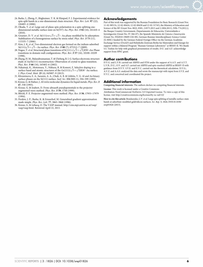
Figure 3 summarizes the results for various adsorbate species. Allspectra have a qualitatively similar appearance but the splitting valuevaries. Momentum splitting at the Fermi level Dkjj ranges from,0.018 A21 obtained for Cs to that of ,0.052 A21 for Tl.Consequently, energy splitting DEF changes in the range from
Figure 1 | Adsorbate-induced transformations in structural and electronic properties of Au/Si(111). STM images and ARPES spectra taken in the firstffiffiffi3p
|ffiffiffi3p
surface Brillouin zone (SBZ) along the M-C0-M direction from (a) pristine Au=Si(111)ffiffiffi3p
|ffiffiffi3p
surface and the same surface after adsorption of
0.15 6 0.05 ML of (b) Tl, (c) In, and (d) Na. Scale of the STM images is 250 3 250 A2, that of the insets is 50 3 50 A2. Note that ARPES data are confined to
the interior of SBZ as exact position of the M point is at 0.546 A21. (e) Atomic arrangement (CHCT model) of the Au=Si(111)ffiffiffi3p
|ffiffiffi3p
surface consisting
of Au trimers (shown by orange circles) and Si trimers (shown by blue circles) residing on Si(111) bilayer (shown by black circles) and sketch of reciprocal
space geometry with boundaries of the firstffiffiffi3p
|ffiffiffi3p
SBZ given by black lines (dashed hexagon depicts the 1 3 1 SBZ). The high symmetry points are
marked by circles.
www.nature.com/scientificreports
SCIENTIFIC REPORTS | 3 : 1826 | DOI: 10.1038/srep01826 2
,100 meV to ,190 meV. From the graph shown in Fig. 3b one canconclude that the splitting value is essentially controlled by positionof the Fermi level, i.e., by the electron filling of the S1 band. Theconcept is illustrated in Fig. 3c where the experimental dots fromFig. 3b are superposed on the SA
1 and SB1 dispersion curves of the
calculated band structure. One can see that by choosing appropriateadsorbate species the Fermi level position can be tuned within therange of ,350 meV (shown by the pink shaded area in Fig. 3c).Position of Fermi level also varies slightly depending on concentra-tion of a given adsorbate.
Figure 4a shows the ARPES Fermi surface of the Tl-adsorbedAu=Si 111ð Þ
ffiffiffi3p
|ffiffiffi3p
. One can clearly see the two Fermi contoursof which the outer (corresponding to the SB
1 band) has an almost
circular shape while the inner (corresponding to the SA1 band) has a
shape of a smoothed hexagon. As the hexagon corners lies at the �C-�Kdirections, these are the directions of the minimal splitting, while thegreatest splitting is at the hexagon sides (i.e., along the �C- �M direc-tions). One can see that the calculated constant energy contours(Fig. 4b) properly reproduce all the principal features of the experi-mentally derived Fermi surface map. The only small deviation thatcan be noticed is the discrepancy between the calculated and experi-mental splitting along the �C-�K direction where theory yields slightlyunderestimated value (Fig. 4c).
Figure 4b also shows the clockwise and counterclockwise spinhelicity for the inner and outer contours, respectively, with abruptchange of the sign for out-of-plane spin component at the �C{�K
Figure 2 | Splitting of dispersion curves measured by ARPES and spin-resolved ARPES. (a) Band structure along the M-C-K of the Tl-adsorbed
Au=Si(111)ffiffiffi3p
|ffiffiffi3p
surface determined with spin-unpolarized ARPES. Data are confined to the interior of SBZ as exact positions of the M and K points
are at 0.546 A21 and 0.630 A21, respectively. (b) Spin-resolved ARPES spectra taken for the same surface at a fixed k | | 5 0.30 A21 in the C-M direction.
Figure 3 | Effect of adsorbate species. (a) Fragments of the ARPES spectra taken in the C-M direction near the Fermi level of the Tl-, In-, Na-, and Cs-
adsorbed Au=Si(111)ffiffiffi3p
|ffiffiffi3p
surfaces. (b) Momentum splitting at the Fermi level Dk | | plotted as a function of the Fermi wave vector kF for SA1 and SB
1bands measured for various species (as indicated in the graph). (c) Calculated band structure along the M-C-K with the experimental dots from (b)
superposed on the SA1 and SB
1 dispersion curves. Surface state bands are shown by filled yellow circles, shaded region indicates projected bulk bands. Range
of the varied Fermi level position is indicated by the pink shaded area.
www.nature.com/scientificreports
SCIENTIFIC REPORTS | 3 : 1826 | DOI: 10.1038/srep01826 3

directions, which is intrinsic feature of the Rashba-split surface statesat hexagonal surfaces12. The detailed spin texture is illustrated inFig. 4d. Figure 4d (upper panel) shows the azimuthal dependenciesof in-plane components in the tangential and normal directions tothe SA
1 and SB1 Fermi contours. One can see that tangential compo-
nents for both bands demonstrate a very similar behavior with sharpmaxima in the �C-�K directions and wide minima around the �C- �Mdirections. The normal component (a signature of the Dresselhausterm) is small for the inner SA
1 band but it becomes noticeable for theouter SB
1 band and demonstrates an undulating behavior. Maximaldeviation of the in-plane spin component from a purely tangential is,3u and ,16u for the SA
1 and SB1 subbands, respectively. For both
bands, the out-of-plane z component (Fig. 4d, lower panel) remainsalmost constant in the wide area near the �C- �M directions andabruptly changes its sign going through zero while crossing the�C-�K directions. As a result, spin has a fully in-plane alignment there.The calculations have also revealed that changing the Fermi levelposition affects the spin texture of the S1 band. Upon the downward
shift of the Fermi level from its highest position, corresponding to Tl-adsorbed surface to its lowest position obtained on Cs-modified Au/Si(111) surface (see pink stripe in Fig. 3c) the maximal deviation ofthe in-plane spin component from a purely tangential increases up to,24u for the SB
1 subband while that for the SA1 subband remains ,3u.
At the same time this shift of the Fermi level leads to decreasingmaximal out-of-plane spin tilt angle from , 68(63)u to , 64(53)ufor the outer(inner) subband.
DiscussionOur results show that chemically very different species, alkali metals,Na and Cs, and heavy group-III metals, In and Tl, when beingadsorbed onto the Au=Si 111ð Þ
ffiffiffi3p
|ffiffiffi3p
surface, affect its structuraland electronic properties in a very similar way, namely, eliminatedomain walls and donate electrons to the metallic S1 surface stateband. DFT calculations for In-adsorbed surface26 showed thatremoval of domain walls is due to a stress-relieving effect producedby In adsorption. However, origin of this effect was not disclosed.
Figure 4 | Fermi surface and spin texture. (a) Symmetrized Fermi surface of the Tl-adsorbed Au=Si(111)ffiffiffi3p
|ffiffiffi3p
surface determined with ARPES. The
k-space area where the ARPES measurements were carried out is outlined by a dashed blue line. (b) Constant energy contours at energy marked by dashed
blue line in Fig. 3c. Arrows along the contours and their length indicate the in-plane spin component. The out-of-plane spin component is indicated by
the colour with red and blue corresponding to the upward and downward directions, respectively. White colour indicates fully in-plane spin alignment.
(c) Azimuthal dependence of the Fermi wave vector kF for the SA1 and SB
1 bands. Experimental and calculated data are presented by dots and solid lines,
respectively. (d) Azimuthal dependencies of the spin components, including in-plane components in the directions tangential and normal to the Fermi
contour (upper panel) and out-of-plane component (lower panel).
www.nature.com/scientificreports
SCIENTIFIC REPORTS | 3 : 1826 | DOI: 10.1038/srep01826 4

Typically, surface lattice stress changes when foreign atoms becomeincorporated directly into the lattice and the greater the size differ-ence between the host and foreign atoms the greater the stress. Thistypical scenario is apparently not held for the present case whereforeign adatoms are not incorporated into the lattice and their atomicsize does not play a decisive role. As an alternative, we suggest thatadsorbates can affect the surface lattice stress by donating electronsto the substrate surface layer. As a result, the top layer possesses anon-compensated charge which means adding a Coulomb repulsionterm into the interactions between surface atoms, hence changing thesurface stress.
We have found a number of adsorbate species (Tl, In, Na, and Cs)which make the Au=Si 111ð Þ
ffiffiffi3p
|ffiffiffi3p
surface suitable for observingsignificant spin-orbit splitting. We believe that the list of such adsor-bates can be extended (at least, at the expense of the left alkali metals).The main requirements for candidate species seem to be as follows.First, they are metals that could easily donate a sufficient amount ofelectrons to the surface state band. This could be attained with spe-cies like monovalent alkali metals with high electropositivity and/orspecies having several valent electrons, as Group-III metals. In thisrespect, it is worth noting the very recent finding that extra Au or Geatoms produce a similar doping effect on Au=Ge 111ð Þ
ffiffiffi3p
|ffiffiffi3p
sur-face30, thus extending further the list of possible candidate species.Second, they have to preserve the original Au trimer structure (whichis believed to be responsible for the spin-splitting effect18) or, in otherwords, they should not form 2D alloys with Au on Si(111) surface.For example, in contrast to In and Tl, the other group-III metals, Aland Ga, are not suitable, as they form binary reconstructions with Au,Au,Alð Þ=Si 111ð Þ3
ffiffiffi3p
|3ffiffiffi3p
31, (Au,Al)/Si(111)2 3 231, andAu,Gað Þ=Si 111ð Þ3
ffiffiffi3p
|3ffiffiffi3p
.As the list is open, many species are expected to produce a similar
effect on the structure and electronic properties of the Au=Si 111ð Þffiffiffi3p
|ffiffiffi3p
surface. However, similarity does not mean identity, thatmakes the family of adsorbate-modified Au=Si 111ð Þ
ffiffiffi3p
|ffiffiffi3p
recon-structions to be a promising playground for exploring spin-splittingeffects as a function of structural parameters tuned by adsorption ofparticular species. On the other hand, they represent a wide set ofsurface systems for the choice of the proper ones for spintronic deviceapplications.
Another degree of freedom for tailoring electronic propertiesstems from ability to intermix Si and Ge into a desired SixGe1–x alloylayer. Though Si and Ge are akin elements and their
ffiffiffi3p
|ffiffiffi3p
-Aureconstructions have the same atomic arrangement, their electronicstructures exhibit essential differences. While the Au=Si 111ð Þffiffiffi
3p
|ffiffiffi3p
surface has a single metallic S1 band, the Au=Ge 111ð Þffiffiffi3p
|ffiffiffi3p
surface in addition to the electronic S1 band has the holebands dispersing up to the Fermi level17,18. The spin textures of the S1
bands for these surfaces are similar but also not identical, namely,contribution of the Dresselhaus terms for the Au=Ge 111ð Þ
ffiffiffi3p
|ffiffiffi3p
is substantially greater19. Thus, the variable Au=SixGe1{x 111ð Þffiffiffi3p
|ffiffiffi3p
surfaces might be a new interesting object for exploringspin-splitting effects in metal monolayers on semiconductor.
MethodsSample preparation method. The STM and ARPES experiments were performed inan ultra-high-vacuum system with a base pressure of ,2.0 3 10210 Torr. Atomically-clean Si(111)7 3 7 surfaces were prepared in situ by flashing to 1280uC after thesamples were first outgassed at 600uC for several hours. Pristine Au=Si 111ð Þ
ffiffiffi3p
|ffiffiffi3p
surfaces were formed by Au deposition onto Si(111)7 3 7 surface held at ,600uC.The adsorbate-modified Au/Si(111) surfaces were prepared by adsorbing 0.15 6
0.05 ML of a given species, In, Na or Cs, onto the surface held at ,350uC. Due tosignificant desorption, deposition of Tl was performed at room temperature followedby annealing at ,350uC. Adsorbate deposition was terminated when STM showsdomain-wall-free surface and LEED displays a sharp
ffiffiffi3p
|ffiffiffi3p
pattern without anyother features.
STM. STM images were acquired using Omicron variable-temperature STM-XAoperating in a constant-current mode. Electrochemically-etched W tips andmechanically cut PtIr tips were used as STM probes after annealing in vacuum.
ARPES and spin-resolved ARPES. ARPES measurements were conducted in theultrahigh vacuum chamber Omicron MULTIPROBE using VG Scienta R3000electron analyzer and high-flux He discharge lamp (hn 5 21.2 eV) with toroidal-grating monochromator as a light source. Spin-resolved ARPES and part of ARPESmeasurements were performed at the novel SR-ARPES facility of RGL at BESSY,U125-2_SGM beamline using VG Scienta R4000 analyzer with Mott detectoroperating at 25 keV.
First-principles calculations. Our calculations were based on DFT as implementedin the Vienna ab initio simulation package VASP32,33, using a planewave basis and theprojector augmented-wave approach34 for describing the electron-ion interaction.The generalized gradient approximation (GGA) of Perdew, Burke, and Ernzerhof(PBE)35 has been used for the exchange correlation (XC) potential. The Hamiltoniancontains the scalar relativistic corrections, and the spin-orbit interaction (SOI) wastaken into account by the second variation method as has been implemented in VASPby Kresse and Lebacq36. To simulate the
ffiffiffi3p
|ffiffiffi3p
-CHCT reconstruction we use a slabconsisting of 12 bilayers. Hydrogen atoms were used to passivate the Si danglingbonds at the bottom of the slab. Both bulk Si lattice constant and the atomic positionswithin the three topmost bilayers of the slab were optimized including SOIself-consistently. The silicon atoms of deeper layers were kept fixed at the bulkcrystalline positions.
1. Sinova, J. et al. Universal intrinsic spin Hall effect. Phys. Rev. Lett. 92, 126603(2004).
2. LaShell, S., McDougall, B. A. & Jensen, E. Spin splitting of an Au(111) surface stateband observed with angle resolved photoelectron spectroscopy. Phys. Rev. Lett.77, 3419–3422 (1996).
3. Hoesch, M. et al. Spin structure of the Shockley surface state on Au(111). Phys.Rev. B 69, 241401 (2004).
4. Koroteev, Y. M. et al. Strong spin-orbit splitting on Bi surfaces. Phys. Rev. Lett. 93,046403 (2004).
5. Kimura, A. et al. Strong Rashba-type spin polarization of the photocurrent frombulk continuum states: Experiment and theory for Bi(111). Phys. Rev. Lett. 105,076804 (2010).
6. Ast, C. R. et al. Giant spin splitting through surface alloying. Phys. Rev. Lett. 98,186807 (2007).
7. Bihlmayer, G., Blugel, S. & Chulkov, E. V. Enhanced Rashba spin-orbit splitting inBi/Ag(111) and Pb/Ag(111) surface alloys from first principles. Phys. Rev. B 75,195414 (2007).
8. Gierz, I. et al. Silicon surface with giant spin splitting. Phys. Rev. Lett. 103 (4),046803–4 (2009).
9. Sakamoto, K. et al. Peculiar Rashba splitting originating from the two-dimensional symmetry of the surface. Phys. Rev. Lett. 103 (15), 156801–4 (2009).
10. Frantzeskakis, E., Pons, S. & Grioni, M. Band structure scenario for the giant spin-orbit splitting observed at the Bi/Si(111) interface. Phys. Rev. B 82 (8), 085440–11(2010).
11. Ohtsubo, Y. et al. Spin-polarized semiconductor surface states localized insubsurface layers. Phys. Rev. B 82 (20), 201307–4 (2010).
12. Sakamoto, K. et al. Abrupt rotation of the Rashba spin to the directionperpendicular to the surface. Phys. Rev. Lett. 102 (9), 096805–4 (2009).
13. Ibanez-Azpiroz, J., Eiguren, A. & Bergara, A. Relativistic effects and fully spin-polarized Fermi surface at the Tl/Si(111) surface. Phys. Rev. B 84 (12), 125435–6(2011).
14. Park, J. et al. Self-assembled nanowires with giant Rashba split band. Phys. Rev.Lett. 110 (3), 036801–5 (2013).
15. Yaji, K. et al. Large Rashba spin plitting of a metallic surface-state band on asemiconductor surface. Nature Commun. 1, 17–5 (2010).
16. Yaji, K., Hatta, S., Aruga, T. & Okuyama, H. Structural and electronic properties of
the Pb=Ge 111ð Þ-bffiffiffi3p
|ffiffiffi3p� �
R300surface studied by PES and first-principles
calculations. Phys. Rev. B 86 (23), 235317–6 (2012).17. Hopfner, P. et al. Electronic band structure of the two-dimensional metallic
electron system Au/Ge(111). Phys. Rev. B 83 (23), 235435–8 (2011).18. Nakatsuji, K. et al. Anisotropic splitting and spin polarization of metallic bands
due to spin-orbit interaction at the Ge 111ð Þffiffiffi3p
|ffiffiffi3p� �
R300-Au surface. Phys.Rev. B 84 (3), 035436–4 (2011).
19. Hopfner, P. et al. Three-dimensional spin rotations at the Fermi surface of astrongly spin-orbit coupled surface system. Phys. Rev. Lett. 108 (18), 186801–5(2012).
20. Ding, Y. G., Chan, C. T. & Ho, K. M. Theoretical investigation of the structure ofthe
ffiffiffi3p
|ffiffiffi3p� �
R30-Au=Si 111ð Þ surface. Surf. Sci. 275 (3), L691–L696 (1992).21. Hsu, C. H., Lin, W. H., Ozolins, V. & Chuang, F. C. Electronic structure of the
indium-adsorbed Au=Si(111)-ffiffiffi3p
|ffiffiffi3p
surface: A first-principles study. Phys.Rev. B 85 (15), 155401–7 (2012).
22. Howes, P. B., Norris, C., Finney, M. S., Vlieg, E. & van Silfhout, R. G. Structure ofGe(111)
ffiffiffi3p
|ffiffiffi3p
{Au determined by surface X-ray-diffraction. Phys. Rev. B 48(3), 1632–1642 (1993).
23. Over, H., Wang, C. P. & Jona, F. Atomic bond configuration ofGe 111ð Þ-
ffiffiffi3p
|ffiffiffi3p� �
R300-Au: A low-energy electron-diffraction study. Phys. Rev.B 51 (7), 4231–4235 (1995).
www.nature.com/scientificreports
SCIENTIFIC REPORTS | 3 : 1826 | DOI: 10.1038/srep01826 5
24. Barke, I., Zheng, F., Rugheimer, T. K. & Himpsel, F. J. Experimental evidence forspin-split bands in a one-dimensional chain structure. Phys. Rev. Lett. 97 (22),226405–4 (2006).
25. Okuda, T. et al. Large out-of-plane spin polarization in a spin-splitting one-dimensional metallic surface state on Si(557)-Au. Phys. Rev. B 82 (16), 161410–4(2010).
26. Gruznev, D. V. et al. Si(111)-a-ffiffiffi3p
|ffiffiffi3p
{Au phase modified by In adsorption:Stabilization of a homogeneous surface by stress relief. Phys. Rev. B 73 (11),115335–7 (2006).
27. Kim, J. K. et al. Two-dimensional electron gas formed on the indium-adsorbedSi(111)
ffiffiffi3p
|ffiffiffi3p
{Au surface. Phys. Rev. B 80 (7), 075312–7 (2009).28. Nagao, T. et al. Structural phase transitions of Si 111ð Þ-
ffiffiffi3p
|ffiffiffi3p� �
R300-Au: Phasetransitions in domain-wall configurations. Phys. Rev. B 57 (16), 10100–10109(1998).
29. Zhang, H. M., Balasubramanian, T. & Uhrberg, R. I. G. Surface electronic structurestudy of Au/Si(111) reconstruction: Observation of crystal-to-glass transition.Phys. Rev. B 66 (16), 165402–6 (2002).
30. Nakatsuji, K., Motomura, Y., Niikura, R. & Komori, F. Selective doping in asurface band and atomic structures of the Ge(111)(
ffiffiffi3p
|ffiffiffi3p
)R30u-Au surface.J. Phys.:Cond. Matt. 25 (4), 045007–9 (2013).
31. Khramtsova, E. A., Saranin, A. A., Chub, A. B. & Lifshits, V. G. Al and Au binarysurface phases on the Si(111) surface. Surf. Sci. 331/333 (1), 594–599 (1995).
32. Kresse, G. & Hafner, J. Ab initio molecular dynamics for liquid metals. Phys. Rev. B47, 558 (1993).
33. Kresse, G. & Joubert, D. From ultrasoft pseudopotentials to the projectoraugmented-wave method. Phys. Rev. B 59, 1758 (1999).
34. Blochl, P. E. Projector augmented-wave method. Phys. Rev. B 50, 17953–17979(1994).
35. Perdew, J. P., Burke, K. & Ernzerhof, M. Generalized gradient approximationmade simple. Phys. Rev. Lett. 77, 3865–3868 (1996).
36. Kresse, G. & Lebacq, O. The VASP manual. http://cms.mpi.univie.ac.at/vasp/vasp/vasp.html. Retrieved April 22, 2013.
AcknowledgementsPart of this work was supported by the Russian Foundation for Basic Research (Grant Nos.11-02-98515r, 12-02-00416, 12-02-00430 and 12-02-31745), the Ministry of Education andScience of the RF (Grant Nos. 8022, 8581, 2.8575.2013 and 2.1004.2011), NSh-774.2012.2,the Basque Country Government, Departamento de Educacion, Universidades eInvestigacion (Grant No. IT-366-07), the Spanish Ministerio de Ciencia e Innovacion(Grant No. FIS2010-19609-C02-00), German-Russian Interdisciplinary Science Center(G-RISC) funded by the German Federal Foreign Office via the German AcademicExchange Service (DAAD) and Helmholtz Zentrum Berlin fur Materialien und Energie forsupport within a bilateral Program ‘‘Russian-German Laboratory’’ at BESSY-II. We thankS.S. Tsirkin for help with graphical presentation of results. D.U. and A.F. acknowledgesupport from SPbU grant.
Author contributionsD.V.G. and L.V.B. carried out ARPES and STM under the support of A.A.Y. and A.Y.T.L.V.B., D.U., O.V. and A.F. carried out ARPES and spin-resolved ARPES at BESSY-II withguidance from D.V.V. S.V.E. and E.V.C. carried out the theoretical calculation. D.V.G.,A.V.Z. and A.A.S. analyzed the data and wrote the manuscript with input from S.V.E. andE.V.C. and conceived and coordinated the project.
Additional informationCompeting financial interests: The authors declare no competing financial interests.
License: This work is licensed under a Creative CommonsAttribution-NonCommercial-NoDerivs 3.0 Unported License. To view a copy of thislicense, visit http://creativecommons.org/licenses/by-nc-nd/3.0/
How to cite this article: Bondarenko, L.V. et al. Large spin splitting of metallic surface-statebands at adsorbate-modified gold/silicon surfaces. Sci. Rep. 3, 1826; DOI:10.1038/srep01826 (2013).
www.nature.com/scientificreports
SCIENTIFIC REPORTS | 3 : 1826 | DOI: 10.1038/srep01826 6
Related Documents