Large-scale statistical analysis of early failures in Cu electromigration, Part II: Scaling behavior and short-length effects Martin Gall, 1,a Meike Hauschildt, 1 and Richard Hernandez 2 1 Freescale Semiconductor, Inc., Hudson Valley Research Park, 2070 Route 52, Hopewell Junction, New York 12533, USA 2 Freescale Semiconductor, Inc., 3501 Ed Bluestein Blvd, MD K10, Austin, Texas 78721, USA Received 30 November 2009; accepted 3 March 2010; published online 13 July 2010 The first part of this study, presented in a separate paper, focused on the early failure mechanisms in down-flow electromigration. Since bimodality can occur at very small percentage levels, specific test structures were designed based on the Wheatstone Bridge technique. The use of these structures enabled a tested sample size past 800,000 for the 90 nm technology node, allowing a direct analysis of electromigration failure mechanisms at the single-digit ppm regime. The activation energy for the down-flow early failure mechanism was determined to be 0.83 0.01 eV, significantly lower than the usually reported activation energy of about 0.90 eV for electromigration-induced diffusion along Cu/SiCN interfaces. Very short experimental lifetimes due to small, slit-shaped voids under vias were found to control the chip lifetime at operating conditions. In this second part of our large-scale, statistical study, we will discuss the electromigration scaling behavior across 90, 65, and 45 nm technologies. Results indicate that the early failure mechanism follows the expected dependency, i.e., the lifetimes scale with the interconnect line height and the critical void size. The slitlike character of the early failure void morphology also raises concerns about the validity of the short-length effect for this mechanism. A very small amount of Cu depletion may cause failure even before a stress gradient is established. We therefore conducted large-scale statistical experiments close to the critical current density-length product jL . The results indicate that at very small failure percentages, the critical product extrapolates to about 2100 300 A / cm for SiCOH-based dielectrics in 90 nm technology. This value represents a decrease from the previously determined jL product of about 3000 500 A / cm for the same dielectric material and technology node, acquired with single link interconnects. Utilizing the advantages of the Wheatstone Bridge technique, the total sample size encompassing 90, 65, and 45 nm technologies was increased past 1.2 10 6 .© 2010 American Institute of Physics. doi:10.1063/1.3374702 I. INTRODUCTION As discussed in the first part of this study, the continuing drive toward smaller interconnect circuitry as well as the introduction of new materials and deposition processes for dielectric and barrier applications results in reliability con- cerns due to electromigration EM. A review of the main factors requiring attention in the analysis of EM failure data can be found there and in the references contained therein. Bimodality for the electron down-flow direction in dual- inlaid Cu interconnects was found to be a major concern for advanced technology nodes. Very short lifetimes due to small, slit-shaped voids under vias were found to control the chip operating lifetimes at use conditions. The objective of this second part of our study is a more thorough investigation of the early failure scaling behavior and the short-length ef- fect. Test structures based on the Wheatstone Bridge WSB technique were used for the 90, 65, and 45 nm technology nodes. Generally, standard single link EM lifetimes are ex- pected to decrease with dimensional scaling, however, the scaling behavior of possible early failure mechanisms has not been investigated thoroughly. Differences in activation energies and current exponents may result in changes for the scaling behavior as well. In addition, short-length effects have rarely been evaluated extensively using a large-scale statistical approach. Given the fact that very small voids un- der vias control the chip lifetime, it is questionable that an EM-induced Cu drift is able to build up a stress gradient which in turn counteracts the electron-driven mass flux. We therefore conducted experiments using 90 nm WSB devices very close to the expected critical current density. Extrapola- tions of Cu drift data, aiming at the expected critical product jL , indicate that the traditional assumption of a linear be- havior with respect to the current density is not valid, i.e., the current exponent does not follow the expected n =1 behavior. Instead, the experimental data suggest a higher exponent of n 1.5. Consequently, extrapolation methods may have to change and we see a reduction in the statistically obtained critical product jL . Possible reasons for these results will be discussed. II. EXPERIMENTAL RESULTS: SCALING BEHAVIOR With continuing scaling of interconnects, EM lifetimes in single link tests were found to decrease even if the current density j was kept constant. 1,2 Both the critical void length and the metal height influence this phenomenon. The former is defined as the void length to create a measurable resistance a Electronic mail: [email protected]. JOURNAL OF APPLIED PHYSICS 108, 013524 2010 0021-8979/2010/1081/013524/6/$30.00 © 2010 American Institute of Physics 108, 013524-1

Welcome message from author
This document is posted to help you gain knowledge. Please leave a comment to let me know what you think about it! Share it to your friends and learn new things together.
Transcript
Large-scale statistical analysis of early failures in Cu electromigration,Part II: Scaling behavior and short-length effects
Martin Gall,1,a� Meike Hauschildt,1 and Richard Hernandez2
1Freescale Semiconductor, Inc., Hudson Valley Research Park, 2070 Route 52, Hopewell Junction,New York 12533, USA2Freescale Semiconductor, Inc., 3501 Ed Bluestein Blvd, MD K10, Austin, Texas 78721, USA
�Received 30 November 2009; accepted 3 March 2010; published online 13 July 2010�
The first part of this study, presented in a separate paper, focused on the early failure mechanismsin down-flow electromigration. Since bimodality can occur at very small percentage levels, specifictest structures were designed based on the Wheatstone Bridge technique. The use of these structuresenabled a tested sample size past 800,000 for the 90 nm technology node, allowing a direct analysisof electromigration failure mechanisms at the single-digit ppm regime. The activation energy for thedown-flow early failure mechanism was determined to be 0.83�0.01 eV, significantly lower thanthe usually reported activation energy of about 0.90 eV for electromigration-induced diffusion alongCu/SiCN interfaces. Very short experimental lifetimes due to small, slit-shaped voids under viaswere found to control the chip lifetime at operating conditions. In this second part of our large-scale,statistical study, we will discuss the electromigration scaling behavior across 90, 65, and 45 nmtechnologies. Results indicate that the early failure mechanism follows the expected dependency,i.e., the lifetimes scale with the interconnect line height and the critical void size. The slitlikecharacter of the early failure void morphology also raises concerns about the validity of theshort-length effect for this mechanism. A very small amount of Cu depletion may cause failure evenbefore a stress gradient is established. We therefore conducted large-scale statistical experimentsclose to the critical current density-length product �jL��. The results indicate that at very smallfailure percentages, the critical product extrapolates to about 2100�300 A /cm for SiCOH-baseddielectrics in 90 nm technology. This value represents a decrease from the previously determined�jL�� product of about 3000�500 A /cm for the same dielectric material and technology node,acquired with single link interconnects. Utilizing the advantages of the Wheatstone Bridgetechnique, the total sample size encompassing 90, 65, and 45 nm technologies was increased past1.2�106. © 2010 American Institute of Physics. �doi:10.1063/1.3374702�
I. INTRODUCTION
As discussed in the first part of this study, the continuingdrive toward smaller interconnect circuitry as well as theintroduction of new materials and deposition processes fordielectric and barrier applications results in reliability con-cerns due to electromigration �EM�. A review of the mainfactors requiring attention in the analysis of EM failure datacan be found there and in the references contained therein.Bimodality for the electron down-flow direction in dual-inlaid Cu interconnects was found to be a major concern foradvanced technology nodes. Very short lifetimes due tosmall, slit-shaped voids under vias were found to control thechip operating lifetimes at use conditions. The objective ofthis second part of our study is a more thorough investigationof the early failure scaling behavior and the short-length ef-fect. Test structures based on the Wheatstone Bridge �WSB�technique were used for the 90, 65, and 45 nm technologynodes. Generally, standard �single link� EM lifetimes are ex-pected to decrease with dimensional scaling, however, thescaling behavior of possible early failure mechanisms hasnot been investigated thoroughly. Differences in activationenergies and current exponents may result in changes for the
scaling behavior as well. In addition, short-length effectshave rarely been evaluated extensively using a large-scalestatistical approach. Given the fact that very small voids un-der vias control the chip lifetime, it is questionable that anEM-induced Cu drift is able to build up a stress gradientwhich in turn counteracts the electron-driven mass flux. Wetherefore conducted experiments using 90 nm WSB devicesvery close to the expected critical current density. Extrapola-tions of Cu drift data, aiming at the expected critical product�jL��, indicate that the traditional assumption of a linear be-havior with respect to the current density is not valid, i.e., thecurrent exponent does not follow the expected n=1 behavior.Instead, the experimental data suggest a higher exponent ofn�1.5. Consequently, extrapolation methods may have tochange and we see a reduction in the statistically obtainedcritical product �jL��. Possible reasons for these results willbe discussed.
II. EXPERIMENTAL RESULTS: SCALING BEHAVIOR
With continuing scaling of interconnects, EM lifetimesin single link tests were found to decrease even if the currentdensity �j� was kept constant.1,2 Both the critical void lengthand the metal height influence this phenomenon. The formeris defined as the void length to create a measurable resistancea�Electronic mail: [email protected].
JOURNAL OF APPLIED PHYSICS 108, 013524 �2010�
0021-8979/2010/108�1�/013524/6/$30.00 © 2010 American Institute of Physics108, 013524-1
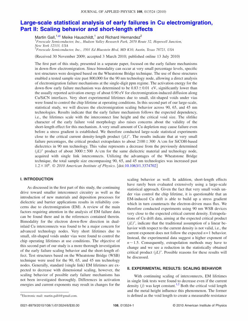
increase in the test line, and it was found to coincide ap-proximately with the via size. Due to a decrease in lineheight with every technology generation, the effective driftvelocity under EM test conditions increases, leading to ear-lier failure. The scaling factor employed to reduce the inter-connect dimensions of each new technology generation, s, istypically on the order of 0.7, i.e., the via sizes, metal heights,and widths are reduced by approximately 30%. The resultingEM lifetimes then scale with about s2, which leads to a re-duction of about 50%. In addition to this geometric scalingbehavior, transistor frequencies as well as front end and backend capacitances tend to increase the needed current densi-ties for each generation. This effect results in even shorterlifetimes. As stated above, early failure mechanisms controlthe chip lifetime at operating conditions. Thus, it is necessaryto evaluate the scaling behavior of early failure phenomena.Figures 1�a� and 1�b� show transmission electron microscopy�TEM� cross-sections of interconnects from the 90 nm and65 nm technologies, respectively. The scaling factors for theline width and height are about 0.75 and 0.6, respectively.Lifetime distributions from down-flow WSB tests for bothgenerations are shown in Fig. 2�a�. The test structures usedfor 65 nm samples were designed differently compared to the90 nm structures. Each sample contains 2448 interconnectscompared to 920 in case of 90 nm technology. Thus, decon-volution of the data, described in detail in part I of this study,is necessary to adequately compare the EM performance.Figure 2�b� displays the deconvoluted lifetime distributionsfor both data sets. The ratio between the 65 and 90 nm life-times at the higher NSD values is approximately 0.5, whichis in good agreement with the dimensional reductions, con-sidering that the via sizes were scaled by about 0.77 in thisparticular case. It is interesting to note that the lifetimes ofthe 65 nm interconnects show a tighter distribution comparedto the 90 nm samples. It is likely that differences in tools andprocesses between the two technologies led to a cleaner in-terface between via and metal interconnect, thus reducing therisk for very early failures. Additional data points are neededthough for further assessment. Figure 3 shows Arrheniusplots for 90 and 65 nm technologies, along with very earlydata for 45 nm technology. Interestingly, the 65 nm samplesyield an activation energy of 0.90�0.02 eV between 225and 325 °C. This value appears significantly higher com-pared to the activation energy of 0.83�0.01 eV measuredfor the early failure mode in 90 nm samples. The 65 nm
number aligns very well with the expected value for EM-induced Cu diffusion along the top Cu/SiCN interface. Theimproved activation energy might also be due to newer toolsets and improved via processing since the 65 nm samplesoriginate from a 300 mm fab compared to the 90 nm materialwhich was processed at a 200 mm fab. It needs to be notedthough that for 65 nm technology a smaller temperaturerange was evaluated, namely 100 °C compared to 175 °Cfor 90 nm. However, even within the smaller temperaturerange between 225–325 °C, the 90 nm technology sampleshad shown the reduced activation energy of about 0.83 eV. Ingeneral, both characteristics, tight distributions and high ac-tivation energy are essential when extrapolating to use con-ditions, especially with dimensional scaling leading to fur-ther reduction in EM lifetimes. Experiments for the 45 nmtechnology node continue and more detailed results will bereported in a forthcoming publication. The very early datashown here indicate an activation energy of about 0.9 eV orhigher, an encouraging value which is in-line with expecta-
FIG. 1. TEM images of �a� 90 nm and �b� 65 nm technology interconnects.
FIG. 2. �Color online� Lifetime distributions for down-flow WSB devicesfor 90 and 65 nm technologies at 325 °C, �a� raw data and �b� deconvoluteddata.
FIG. 3. �Color online� Arrhenius plots for 90, 65, and 45 nm WSB data.
013524-2 Gall, Hauschildt, and Hernandez J. Appl. Phys. 108, 013524 �2010�
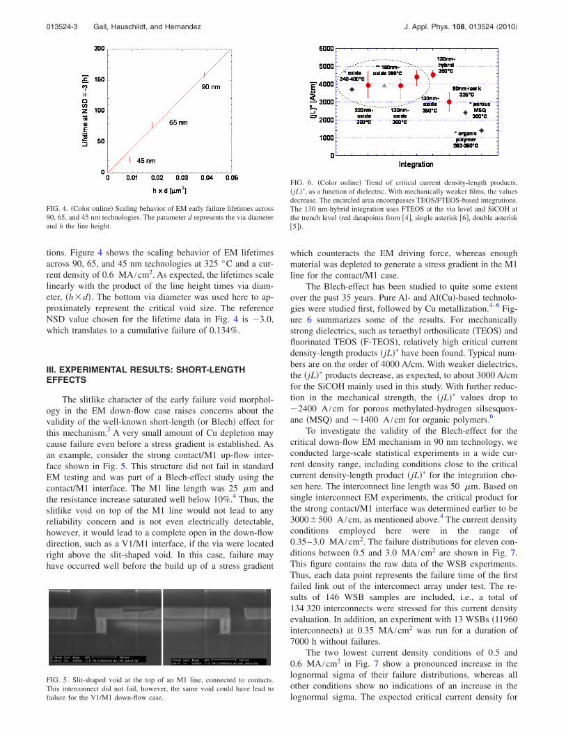
tions. Figure 4 shows the scaling behavior of EM lifetimesacross 90, 65, and 45 nm technologies at 325 °C and a cur-rent density of 0.6 MA /cm2. As expected, the lifetimes scalelinearly with the product of the line height times via diam-eter, �h�d�. The bottom via diameter was used here to ap-proximately represent the critical void size. The referenceNSD value chosen for the lifetime data in Fig. 4 is �3.0,which translates to a cumulative failure of 0.134%.
III. EXPERIMENTAL RESULTS: SHORT-LENGTHEFFECTS
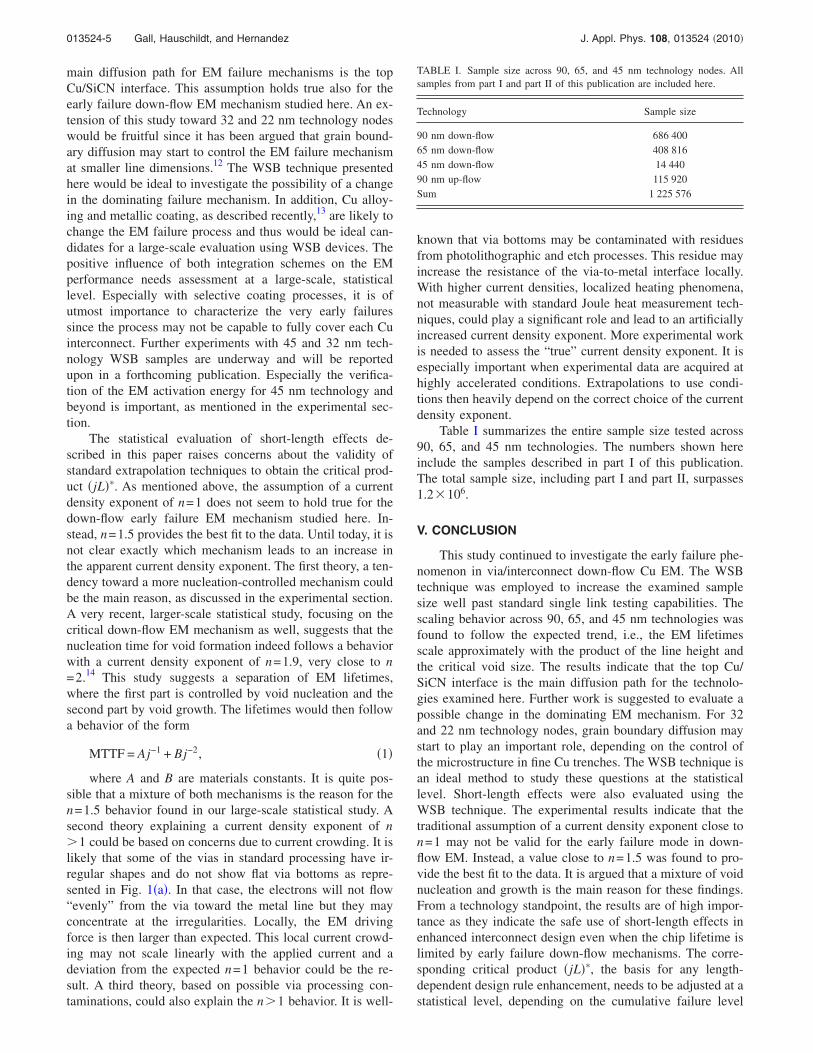
The slitlike character of the early failure void morphol-ogy in the EM down-flow case raises concerns about thevalidity of the well-known short-length �or Blech� effect forthis mechanism.3 A very small amount of Cu depletion maycause failure even before a stress gradient is established. Asan example, consider the strong contact/M1 up-flow inter-face shown in Fig. 5. This structure did not fail in standardEM testing and was part of a Blech-effect study using thecontact/M1 interface. The M1 line length was 25 �m andthe resistance increase saturated well below 10%.4 Thus, theslitlike void on top of the M1 line would not lead to anyreliability concern and is not even electrically detectable,however, it would lead to a complete open in the down-flowdirection, such as a V1/M1 interface, if the via were locatedright above the slit-shaped void. In this case, failure mayhave occurred well before the build up of a stress gradient
which counteracts the EM driving force, whereas enoughmaterial was depleted to generate a stress gradient in the M1line for the contact/M1 case.
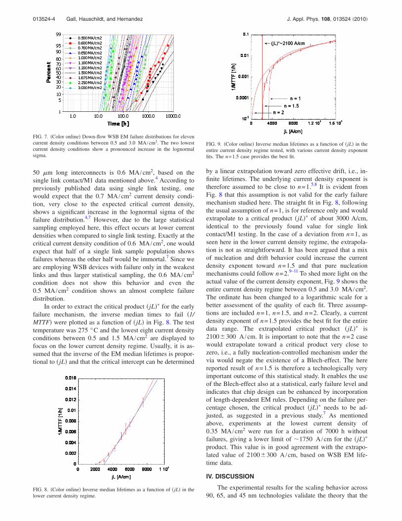
The Blech-effect has been studied to quite some extentover the past 35 years. Pure Al- and Al�Cu�-based technolo-gies were studied first, followed by Cu metallization.4–6 Fig-ure 6 summarizes some of the results. For mechanicallystrong dielectrics, such as teraethyl orthosilicate �TEOS� andfluorinated TEOS �F-TEOS�, relatively high critical currentdensity-length products �jL�� have been found. Typical num-bers are on the order of 4000 A/cm. With weaker dielectrics,the �jL�� products decrease, as expected, to about 3000 A/cmfor the SiCOH mainly used in this study. With further reduc-tion in the mechanical strength, the �jL�� values drop to�2400 A /cm for porous methylated-hydrogen silsesquox-ane �MSQ� and �1400 A /cm for organic polymers.6
To investigate the validity of the Blech-effect for thecritical down-flow EM mechanism in 90 nm technology, weconducted large-scale statistical experiments in a wide cur-rent density range, including conditions close to the criticalcurrent density-length product �jL�� for the integration cho-sen here. The interconnect line length was 50 �m. Based onsingle interconnect EM experiments, the critical product forthe strong contact/M1 interface was determined earlier to be3000�500 A /cm, as mentioned above.4 The current densityconditions employed here were in the range of0.35–3.0 MA /cm2. The failure distributions for eleven con-ditions between 0.5 and 3.0 MA /cm2 are shown in Fig. 7.This figure contains the raw data of the WSB experiments.Thus, each data point represents the failure time of the firstfailed link out of the interconnect array under test. The re-sults of 146 WSB samples are included, i.e., a total of134 320 interconnects were stressed for this current densityevaluation. In addition, an experiment with 13 WSBs �11960interconnects� at 0.35 MA /cm2 was run for a duration of7000 h without failures.
The two lowest current density conditions of 0.5 and0.6 MA /cm2 in Fig. 7 show a pronounced increase in thelognormal sigma of their failure distributions, whereas allother conditions show no indications of an increase in thelognormal sigma. The expected critical current density for
FIG. 4. �Color online� Scaling behavior of EM early failure lifetimes across90, 65, and 45 nm technologies. The parameter d represents the via diameterand h the line height.
FIG. 5. Slit-shaped void at the top of an M1 line, connected to contacts.This interconnect did not fail, however, the same void could have lead tofailure for the V1/M1 down-flow case.
FIG. 6. �Color online� Trend of critical current density-length products,�jL��, as a function of dielectric. With mechanically weaker films, the valuesdecrease. The encircled area encompasses TEOS/FTEOS-based integrations.The 130 nm-hybrid integration uses FTEOS at the via level and SiCOH atthe trench level �red datapoints from �4�, single asterisk �6�, double asterisk�5��.
013524-3 Gall, Hauschildt, and Hernandez J. Appl. Phys. 108, 013524 �2010�
50 �m long interconnects is 0.6 MA /cm2, based on thesingle link contact/M1 data mentioned above.4 According topreviously published data using single link testing, onewould expect that the 0.7 MA /cm2 current density condi-tion, very close to the expected critical current density,shows a significant increase in the lognormal sigma of thefailure distribution.4,7 However, due to the large statisticalsampling employed here, this effect occurs at lower currentdensities when compared to single link testing. Exactly at thecritical current density condition of 0.6 MA /cm2, one wouldexpect that half of a single link sample population showsfailures whereas the other half would be immortal.7 Since weare employing WSB devices with failure only in the weakestlinks and thus larger statistical sampling, the 0.6 MA /cm2
condition does not show this behavior and even the0.5 MA /cm2 condition shows an almost complete failuredistribution.
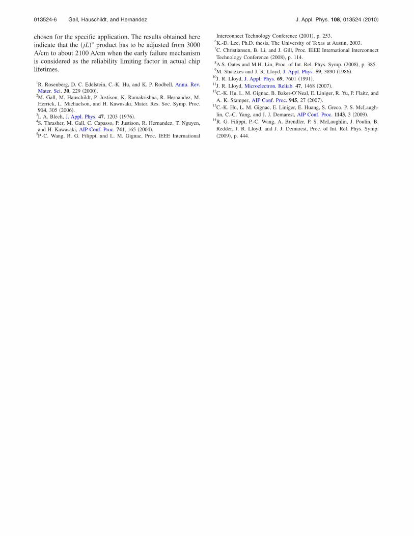
In order to extract the critical product �jL�� for the earlyfailure mechanism, the inverse median times to fail �1/MTTF� were plotted as a function of �jL� in Fig. 8. The testtemperature was 275 °C and the lowest eight current densityconditions between 0.5 and 1.5 MA /cm2 are displayed tofocus on the lower current density regime. Usually, it is as-sumed that the inverse of the EM median lifetimes is propor-tional to �jL� and that the critical intercept can be determined
by a linear extrapolation toward zero effective drift, i.e., in-finite lifetimes. The underlying current density exponent istherefore assumed to be close to n=1.5,8 It is evident fromFig. 8 that this assumption is not valid for the early failuremechanism studied here. The straight fit in Fig. 8, followingthe usual assumption of n=1, is for reference only and wouldextrapolate to a critical product �jL�� of about 3000 A/cm,identical to the previously found value for single linkcontact/M1 testing. In the case of a deviation from n=1, asseen here in the lower current density regime, the extrapola-tion is not as straightforward. It has been argued that a mixof nucleation and drift behavior could increase the currentdensity exponent toward n=1.5 and that pure nucleationmechanisms could follow n=2.9–11 To shed more light on theactual value of the current density exponent, Fig. 9 shows theentire current density regime between 0.5 and 3.0 MA /cm2.The ordinate has been changed to a logarithmic scale for abetter assessment of the quality of each fit. Three assump-tions are included n=1, n=1.5, and n=2. Clearly, a currentdensity exponent of n=1.5 provides the best fit for the entiredata range. The extrapolated critical product �jL�� is2100�300 A /cm. It is important to note that the n=2 casewould extrapolate toward a critical product very close tozero, i.e., a fully nucleation-controlled mechanism under thevia would negate the existence of a Blech-effect. The herereported result of n=1.5 is therefore a technologically veryimportant outcome of this statistical study. It enables the useof the Blech-effect also at a statistical, early failure level andindicates that chip design can be enhanced by incorporationof length-dependent EM rules. Depending on the failure per-centage chosen, the critical product �jL�� needs to be ad-justed, as suggested in a previous study.7 As mentionedabove, experiments at the lowest current density of0.35 MA /cm2 were run for a duration of 7000 h withoutfailures, giving a lower limit of �1750 A /cm for the �jL��
product. This value is in good agreement with the extrapo-lated value of 2100�300 A /cm, based on WSB EM life-time data.
IV. DISCUSSION
The experimental results for the scaling behavior across90, 65, and 45 nm technologies validate the theory that the
FIG. 7. �Color online� Down-flow WSB EM failure distributions for elevencurrent density conditions between 0.5 and 3.0 MA /cm2. The two lowestcurrent density conditions show a pronounced increase in the lognormalsigma.
FIG. 8. �Color online� Inverse median lifetimes as a function of �jL� in thelower current density regime.
FIG. 9. �Color online� Inverse median lifetimes as a function of �jL� in theentire current density regime tested, with various current density exponentfits. The n=1.5 case provides the best fit.
013524-4 Gall, Hauschildt, and Hernandez J. Appl. Phys. 108, 013524 �2010�
main diffusion path for EM failure mechanisms is the topCu/SiCN interface. This assumption holds true also for theearly failure down-flow EM mechanism studied here. An ex-tension of this study toward 32 and 22 nm technology nodeswould be fruitful since it has been argued that grain bound-ary diffusion may start to control the EM failure mechanismat smaller line dimensions.12 The WSB technique presentedhere would be ideal to investigate the possibility of a changein the dominating failure mechanism. In addition, Cu alloy-ing and metallic coating, as described recently,13 are likely tochange the EM failure process and thus would be ideal can-didates for a large-scale evaluation using WSB devices. Thepositive influence of both integration schemes on the EMperformance needs assessment at a large-scale, statisticallevel. Especially with selective coating processes, it is ofutmost importance to characterize the very early failuressince the process may not be capable to fully cover each Cuinterconnect. Further experiments with 45 and 32 nm tech-nology WSB samples are underway and will be reportedupon in a forthcoming publication. Especially the verifica-tion of the EM activation energy for 45 nm technology andbeyond is important, as mentioned in the experimental sec-tion.
The statistical evaluation of short-length effects de-scribed in this paper raises concerns about the validity ofstandard extrapolation techniques to obtain the critical prod-uct �jL��. As mentioned above, the assumption of a currentdensity exponent of n=1 does not seem to hold true for thedown-flow early failure EM mechanism studied here. In-stead, n=1.5 provides the best fit to the data. Until today, it isnot clear exactly which mechanism leads to an increase inthe apparent current density exponent. The first theory, a ten-dency toward a more nucleation-controlled mechanism couldbe the main reason, as discussed in the experimental section.A very recent, larger-scale statistical study, focusing on thecritical down-flow EM mechanism as well, suggests that thenucleation time for void formation indeed follows a behaviorwith a current density exponent of n=1.9, very close to n=2.14 This study suggests a separation of EM lifetimes,where the first part is controlled by void nucleation and thesecond part by void growth. The lifetimes would then followa behavior of the form
MTTF = Aj−1 + Bj−2, �1�
where A and B are materials constants. It is quite pos-sible that a mixture of both mechanisms is the reason for then=1.5 behavior found in our large-scale statistical study. Asecond theory explaining a current density exponent of n�1 could be based on concerns due to current crowding. It islikely that some of the vias in standard processing have ir-regular shapes and do not show flat via bottoms as repre-sented in Fig. 1�a�. In that case, the electrons will not flow“evenly” from the via toward the metal line but they mayconcentrate at the irregularities. Locally, the EM drivingforce is then larger than expected. This local current crowd-ing may not scale linearly with the applied current and adeviation from the expected n=1 behavior could be the re-sult. A third theory, based on possible via processing con-taminations, could also explain the n�1 behavior. It is well-
known that via bottoms may be contaminated with residuesfrom photolithographic and etch processes. This residue mayincrease the resistance of the via-to-metal interface locally.With higher current densities, localized heating phenomena,not measurable with standard Joule heat measurement tech-niques, could play a significant role and lead to an artificiallyincreased current density exponent. More experimental workis needed to assess the “true” current density exponent. It isespecially important when experimental data are acquired athighly accelerated conditions. Extrapolations to use condi-tions then heavily depend on the correct choice of the currentdensity exponent.
Table I summarizes the entire sample size tested across90, 65, and 45 nm technologies. The numbers shown hereinclude the samples described in part I of this publication.The total sample size, including part I and part II, surpasses1.2�106.
V. CONCLUSION
This study continued to investigate the early failure phe-nomenon in via/interconnect down-flow Cu EM. The WSBtechnique was employed to increase the examined samplesize well past standard single link testing capabilities. Thescaling behavior across 90, 65, and 45 nm technologies wasfound to follow the expected trend, i.e., the EM lifetimesscale approximately with the product of the line height andthe critical void size. The results indicate that the top Cu/SiCN interface is the main diffusion path for the technolo-gies examined here. Further work is suggested to evaluate apossible change in the dominating EM mechanism. For 32and 22 nm technology nodes, grain boundary diffusion maystart to play an important role, depending on the control ofthe microstructure in fine Cu trenches. The WSB technique isan ideal method to study these questions at the statisticallevel. Short-length effects were also evaluated using theWSB technique. The experimental results indicate that thetraditional assumption of a current density exponent close ton=1 may not be valid for the early failure mode in down-flow EM. Instead, a value close to n=1.5 was found to pro-vide the best fit to the data. It is argued that a mixture of voidnucleation and growth is the main reason for these findings.From a technology standpoint, the results are of high impor-tance as they indicate the safe use of short-length effects inenhanced interconnect design even when the chip lifetime islimited by early failure down-flow mechanisms. The corre-sponding critical product �jL��, the basis for any length-dependent design rule enhancement, needs to be adjusted at astatistical level, depending on the cumulative failure level
TABLE I. Sample size across 90, 65, and 45 nm technology nodes. Allsamples from part I and part II of this publication are included here.
Technology Sample size
90 nm down-flow 686 40065 nm down-flow 408 81645 nm down-flow 14 44090 nm up-flow 115 920Sum 1 225 576
013524-5 Gall, Hauschildt, and Hernandez J. Appl. Phys. 108, 013524 �2010�
chosen for the specific application. The results obtained hereindicate that the �jL�� product has to be adjusted from 3000A/cm to about 2100 A/cm when the early failure mechanismis considered as the reliability limiting factor in actual chiplifetimes.
1R. Rosenberg, D. C. Edelstein, C.-K. Hu, and K. P. Rodbell, Annu. Rev.Mater. Sci. 30, 229 �2000�.
2M. Gall, M. Hauschildt, P. Justison, K. Ramakrishna, R. Hernandez, M.Herrick, L. Michaelson, and H. Kawasaki, Mater. Res. Soc. Symp. Proc.914, 305 �2006�.
3I. A. Blech, J. Appl. Phys. 47, 1203 �1976�.4S. Thrasher, M. Gall, C. Capasso, P. Justison, R. Hernandez, T. Nguyen,and H. Kawasaki, AIP Conf. Proc. 741, 165 �2004�.
5P.-C. Wang, R. G. Filippi, and L. M. Gignac, Proc. IEEE International
Interconnect Technology Conference �2001�, p. 253.6K.-D. Lee, Ph.D. thesis, The University of Texas at Austin, 2003.7C. Christiansen, B. Li, and J. Gill, Proc. IEEE International InterconnectTechnology Conference �2008�, p. 114.
8A.S. Oates and M.H. Lin, Proc. of Int. Rel. Phys. Symp. �2008�, p. 385.9M. Shatzkes and J. R. Lloyd, J. Appl. Phys. 59, 3890 �1986�.
10J. R. Lloyd, J. Appl. Phys. 69, 7601 �1991�.11J. R. Lloyd, Microelectron. Reliab. 47, 1468 �2007�.12C.-K. Hu, L. M. Gignac, B. Baker-O’Neal, E. Liniger, R. Yu, P. Flaitz, and
A. K. Stamper, AIP Conf. Proc. 945, 27 �2007�.13C.-K. Hu, L. M. Gignac, E. Liniger, E. Huang, S. Greco, P. S. McLaugh-
lin, C.-C. Yang, and J. J. Demarest, AIP Conf. Proc. 1143, 3 �2009�.14R. G. Filippi, P.-C. Wang, A. Brendler, P. S. McLaughlin, J. Poulin, B.
Redder, J. R. Lloyd, and J. J. Demarest, Proc. of Int. Rel. Phys. Symp.�2009�, p. 444.
013524-6 Gall, Hauschildt, and Hernandez J. Appl. Phys. 108, 013524 �2010�
Related Documents