Lab 1 Introduction to Quartus II

Welcome message from author
This document is posted to help you gain knowledge. Please leave a comment to let me know what you think about it! Share it to your friends and learn new things together.
Transcript
Lab 1
Introduction to Quartus II
Lab 1 – Introduction to Quartus II
This lab is designed to familiarize you with using many of the common aspects of the Quartus II software through a complete design phase. You will create a new project, create a new vhdl file, use the MegaWizard Plug-In Manager, compile the design, plan and manage I/O assignments, apply timing analysis using the TimeQuest Timing Analyzer, write Synopsys Design Contraint (SDC) files, and program a design onto the Altera DE2 Development Board.
1-1
Task 1: Create a New Project
1. Start the Quartus II software.From the Windows Start Menu, select:All Programs → Other Apps → Altera → Quartus II 9.1 → Quartus II 9.1 (32-Bit)
2. Start the New Project Wizard.If the opening splash screen is displayed, select: Create a New Project (New Project Wizard),otherwise from the Quartus II Menu Bar select: File → New Project Wizard.
3. Select the Working Directory and Project Name.
Working Directory H:\Altera_Training\Lab1
Project Name Lab1
Top-Level Deign Entity
Lab1
Click Next to advance to page 2 of the New Project Wizard.Note: A window may pop up stating that the chosen working directory does not exist. Click Yes to create it.
1-2
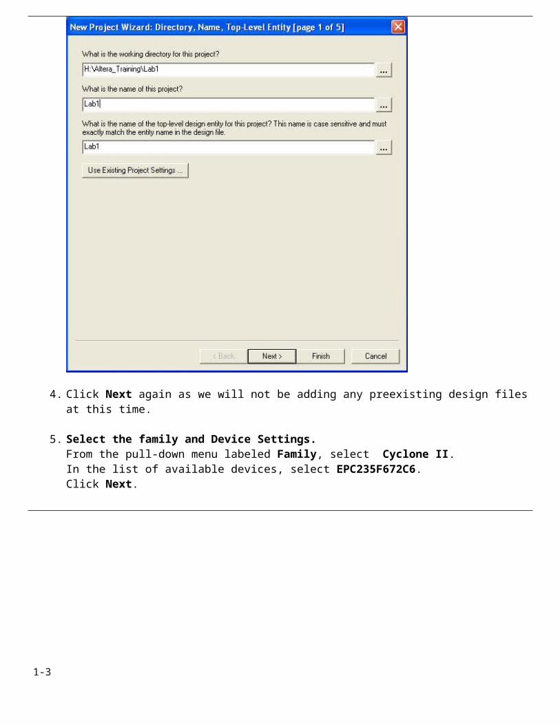
4. Click Next again as we will not be adding any preexisting design files at this time.
5. Select the family and Device Settings.From the pull-down menu labeled Family, select Cyclone II.In the list of available devices, select EPC235F672C6.Click Next.
1-3

6. Click Next again as we will not be using any third party EDA tools.
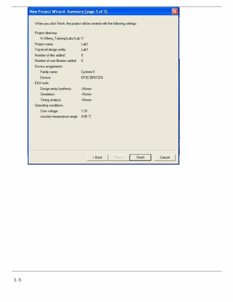
7. Click Finish to complete the New Project Wizard.
1-4
Task 2: Create, Add, and Compile Design Files
1-5
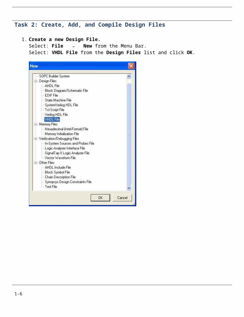
1. Create a new Design File.Select: File → New from the Menu Bar.Select: VHDL File from the Design Files list and click OK.
2. Copy and paste the following code into your new VHDL file, then save it by selecting File →
1-6
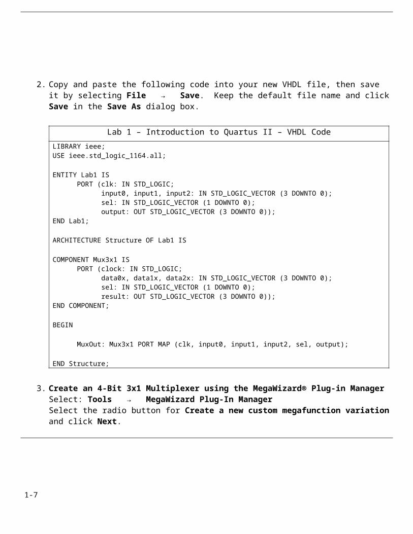
Save. Keep the default file name and click Save in the Save As dialog box.
Lab 1 – Introduction to Quartus II – VHDL Code
LIBRARY ieee;USE ieee.std_logic_1164.all;
ENTITY Lab1 ISPORT (clk: IN STD_LOGIC; input0, input1, input2: IN STD_LOGIC_VECTOR (3 DOWNTO 0); sel: IN STD_LOGIC_VECTOR (1 DOWNTO 0); output: OUT STD_LOGIC_VECTOR (3 DOWNTO 0));
END Lab1;
ARCHITECTURE Structure OF Lab1 IS
COMPONENT Mux3x1 ISPORT (clock: IN STD_LOGIC; data0x, data1x, data2x: IN STD_LOGIC_VECTOR (3 DOWNTO 0); sel: IN STD_LOGIC_VECTOR (1 DOWNTO 0); result: OUT STD_LOGIC_VECTOR (3 DOWNTO 0));
END COMPONENT;
BEGIN
MuxOut: Mux3x1 PORT MAP (clk, input0, input1, input2, sel, output);
END Structure;
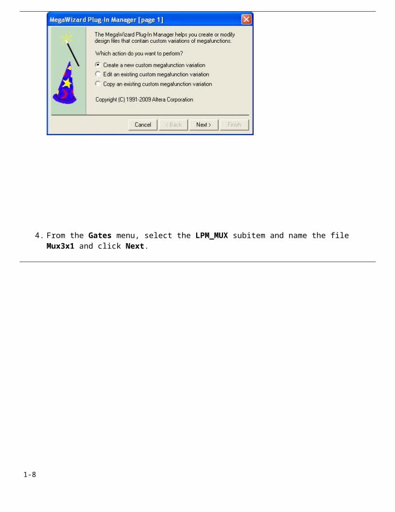
3. Create an 4-Bit 3x1 Multiplexer using the MegaWizard® Plug-in ManagerSelect: Tools → MegaWizard Plug-In ManagerSelect the radio button for Create a new custom megafunction variation and click Next.
1-7
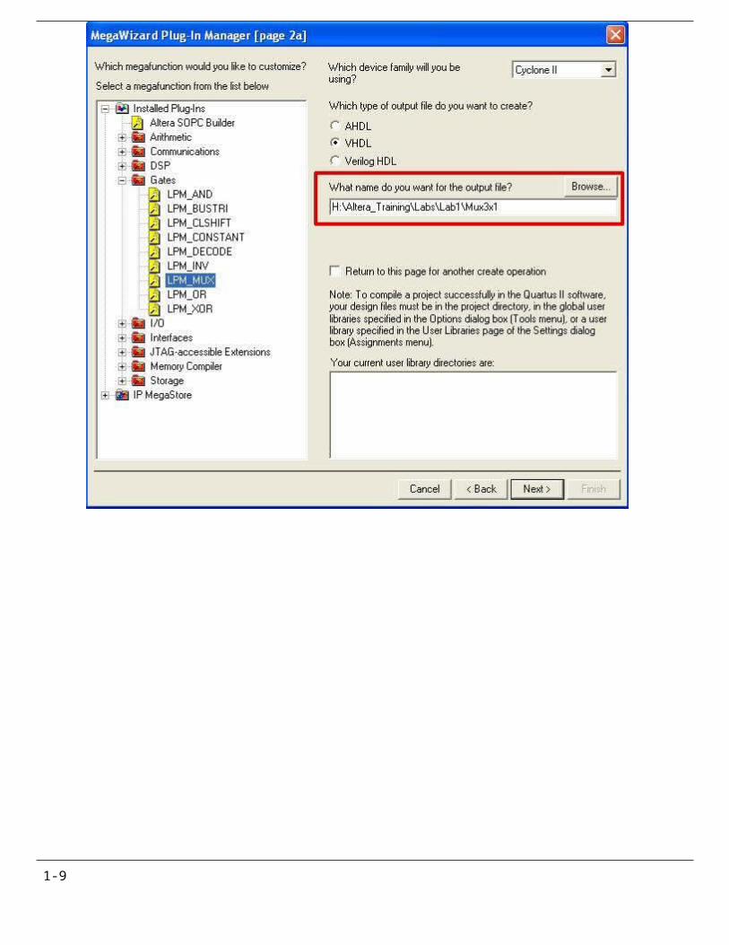
4. From the Gates menu, select the LPM_MUX subitem and name the file Mux3x1 and click Next.
1-8
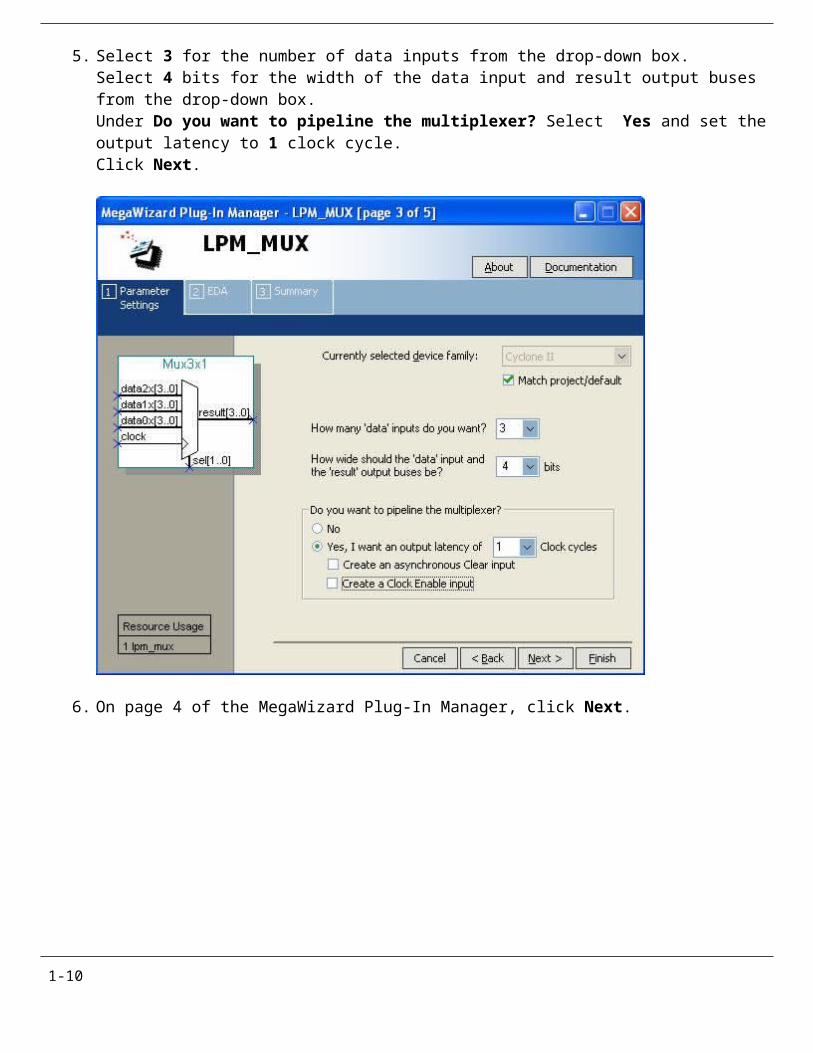
5. Select 3 for the number of data inputs from the drop-down box.Select 4 bits for the width of the data input and result output buses from the drop-down box.Under Do you want to pipeline the multiplexer? Select Yes and set the output latency to 1 clock cycle.Click Next.
6. On page 4 of the MegaWizard Plug-In Manager, click Next.
1-9
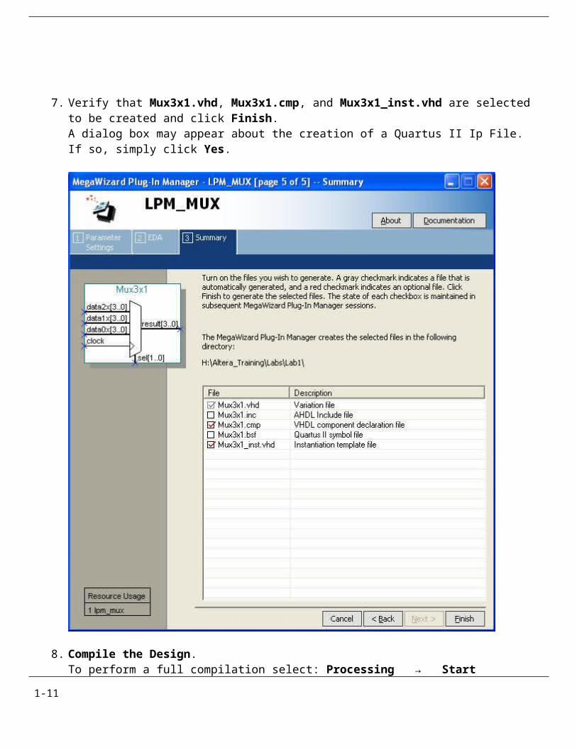
7. Verify that Mux3x1.vhd, Mux3x1.cmp, and Mux3x1_inst.vhd are selected to be created and click Finish.A dialog box may appear about the creation of a Quartus II Ip File. If so, simply click Yes.
8. Compile the Design.To perform a full compilation select: Processing → Start Compilation
Alternatively, select the Start Compilation button on the toolbarYou may ignore any warnings that may appear at this time.
1-10
Task 3: Assign Pins
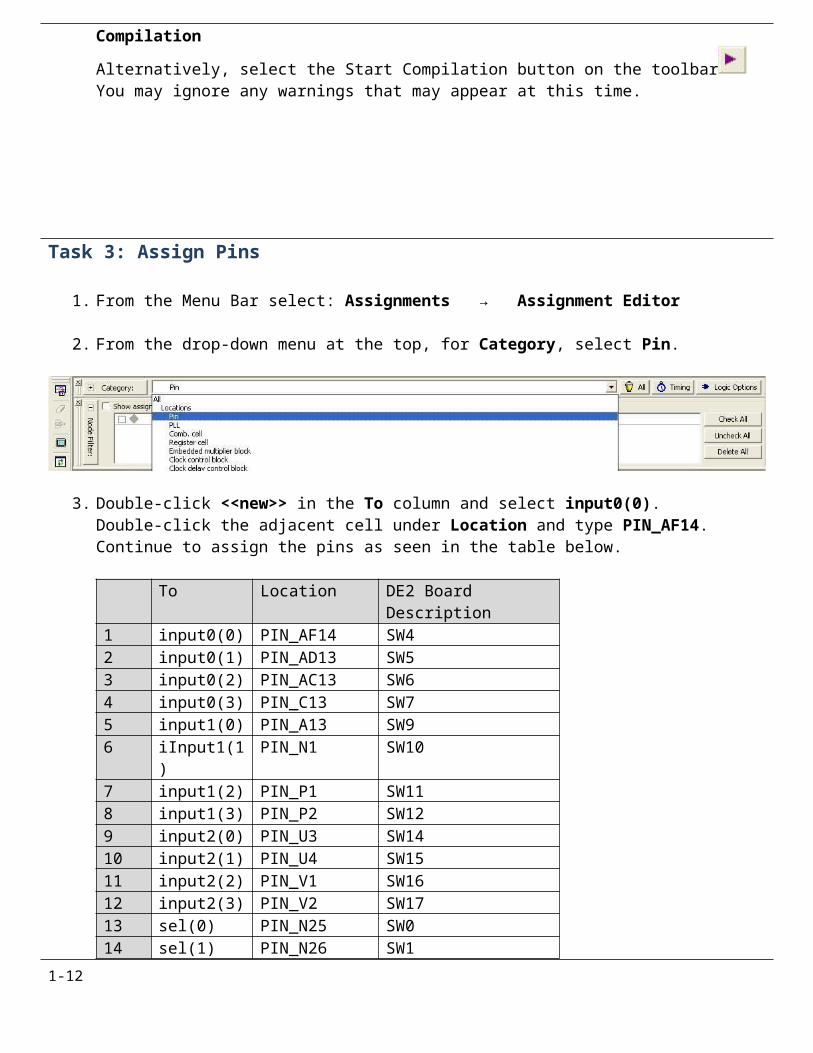
1. From the Menu Bar select: Assignments → Assignment Editor
2. From the drop-down menu at the top, for Category, select Pin.
3. Double-click <<new>> in the To column and select input0(0).Double-click the adjacent cell under Location and type PIN_AF14.Continue to assign the pins as seen in the table below.
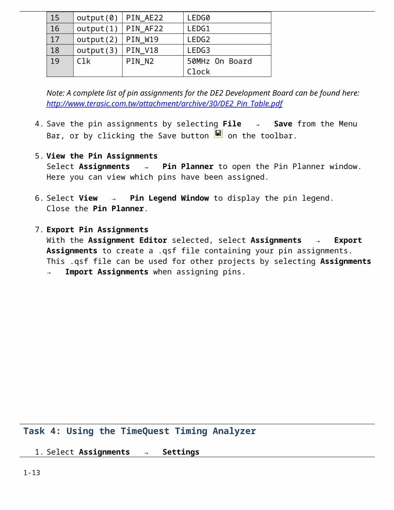
To Location DE2 Board Description1 input0(0) PIN_AF14 SW42 input0(1) PIN_AD13 SW53 input0(2) PIN_AC13 SW64 input0(3) PIN_C13 SW75 input1(0) PIN_A13 SW96 iInput1(1) PIN_N1 SW107 input1(2) PIN_P1 SW118 input1(3) PIN_P2 SW129 input2(0) PIN_U3 SW1410 input2(1) PIN_U4 SW1511 input2(2) PIN_V1 SW1612 input2(3) PIN_V2 SW1713 sel(0) PIN_N25 SW014 sel(1) PIN_N26 SW115 output(0) PIN_AE22 LEDG016 output(1) PIN_AF22 LEDG117 output(2) PIN_W19 LEDG218 output(3) PIN_V18 LEDG319 Clk PIN_N2 50MHz On Board Clock
Note: A complete list of pin assignments for the DE2 Development Board can be found here: http://www.terasic.com.tw/attachment/archive/30/DE2_Pin_Table.pdf
4. Save the pin assignments by selecting File → Save from the Menu Bar, or by clicking the Save
button on the toolbar.
5. View the Pin AssignmentsSelect Assignments → Pin Planner to open the Pin Planner window.Here you can view which pins have been assigned.
1-11
6. Select View → Pin Legend Window to display the pin legend.Close the Pin Planner.
7. Export Pin AssignmentsWith the Assignment Editor selected, select Assignments → Export Assignments to create a .qsf file containing your pin assignments. This .qsf file can be used for other projects by selecting Assignments → Import Assignments when assigning pins.
Task 4: Using the TimeQuest Timing Analyzer
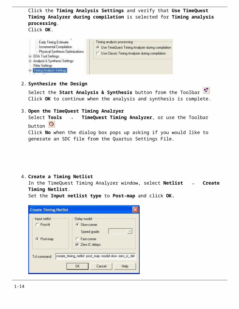
1. Select Assignments → SettingsClick the Timing Analysis Settings and verify that Use TimeQuest Timing Analyzer during compilation is selected for Timing analysis processing.Click OK.
2. Synthesize the Design
Select the Start Analysis & Synthesis button from the Toolbar Click OK to continue when the analysis and synthesis is complete.
3. Open the TimeQuest Timing Analzyer
Select Tools → TimeQuest Timing Analyzer, or use the Toolbar button Click No when the dialog box pops up asking if you would like to generate an SDC file from the Quartus Settings File.
1-12
4. Create a Timing NetlistIn the TimeQuest Timing Analyzer window, select Netlist → Create Timing Netlist.Set the Input netlist type to Post-map and click OK.
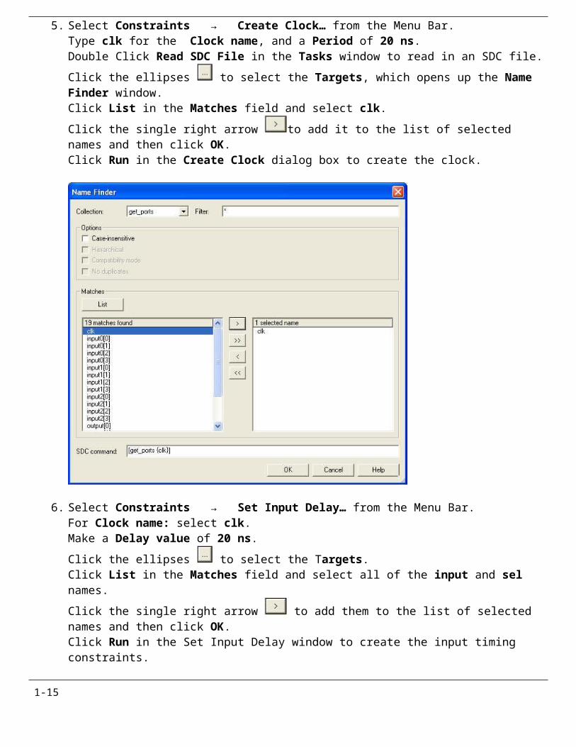
5. Select Constraints → Create Clock… from the Menu Bar.Type clk for the Clock name, and a Period of 20 ns.Double Click Read SDC File in the Tasks window to read in an SDC file.
Click the ellipses to select the Targets, which opens up the Name Finder window.Click List in the Matches field and select clk.
Click the single right arrow to add it to the list of selected names and then click OK.Click Run in the Create Clock dialog box to create the clock.
1-13
6. Select Constraints → Set Input Delay… from the Menu Bar.For Clock name: select clk.Make a Delay value of 20 ns.
Click the ellipses to select the Targets.Click List in the Matches field and select all of the input and sel names.
Click the single right arrow to add them to the list of selected names and then click OK.Click Run in the Set Input Delay window to create the input timing constraints.
1-14
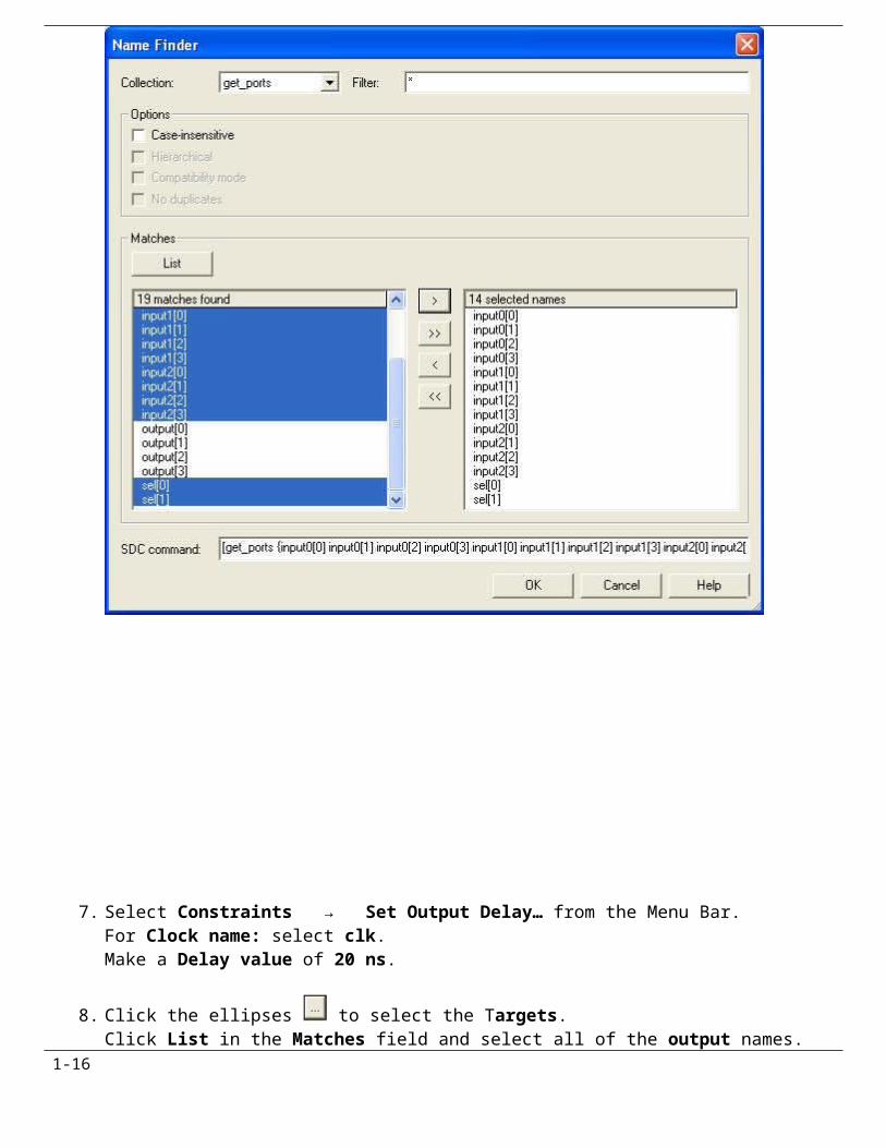
7. Select Constraints → Set Output Delay… from the Menu Bar.For Clock name: select clk.Make a Delay value of 20 ns.
8. Click the ellipses to select the Targets.
Click List in the Matches field and select all of the output names.
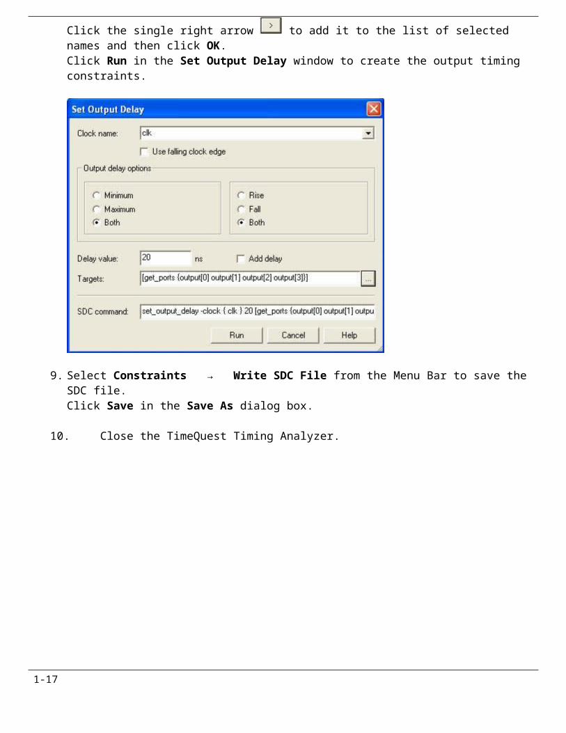
Click the single right arrow to add it to the list of selected names and then click OK.Click Run in the Set Output Delay window to create the output timing constraints.
9. Select Constraints → Write SDC File from the Menu Bar to save the SDC file.Click Save in the Save As dialog box.
10. Close the TimeQuest Timing Analyzer.
1-15
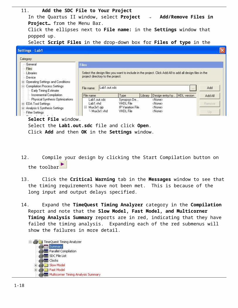
11. Add the SDC File to Your ProjectIn the Quartus II window, select Project → Add/Remove Files in Project… from the Menu Bar.Click the ellipses next to File name: in the Settings window that popped up.Select Script Files in the drop-down box for Files of type in the Select File window.Select the Lab1.out.sdc file and click Open.Click Add and then OK in the Settings window.
12. Compile your design by clicking the Start Compilation button on the toolbar
13. Click the Critical Warning tab in the Messages window to see that the timing requirements have not been met. This is because of the long input and output delays specified.
14. Expand the TimeQuest Timing Analyzer category in the Compilation Report and note that the Slow Model, Fast Model, and Multicorner Timing Analysis Summary reports are in red, indicating that they have failed the timing analysis. Expanding each of the red submenus will show the failures in more detail.
1-16
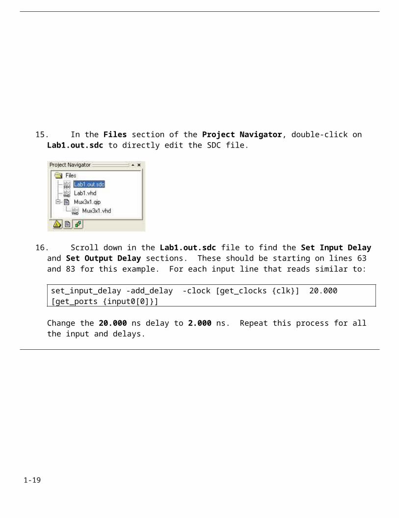
15. In the Files section of the Project Navigator, double-click on Lab1.out.sdc to directly edit the SDC file.
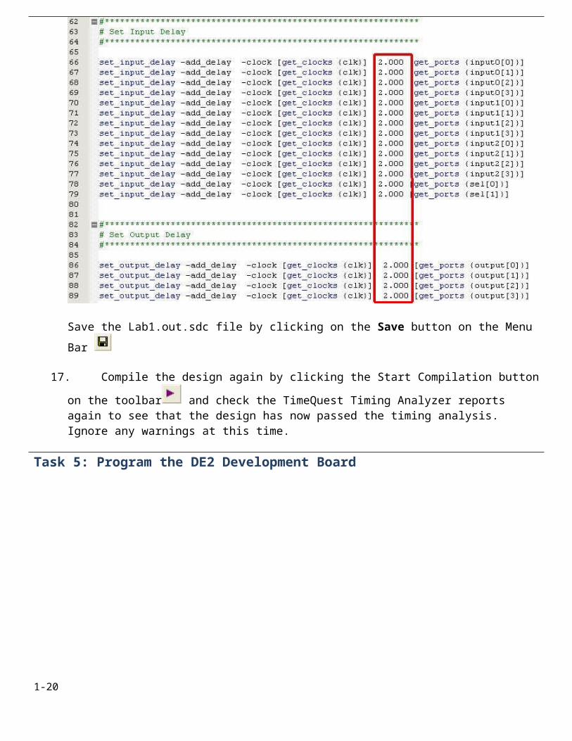
16. Scroll down in the Lab1.out.sdc file to find the Set Input Delay and Set Output Delay sections. These should be starting on lines 63 and 83 for this example. For each input line that reads similar to:
set_input_delay -add_delay -clock [get_clocks {clk}] 20.000 [get_ports {input0[0]}]
Change the 20.000 ns delay to 2.000 ns. Repeat this process for all the input and delays.
1-17
Save the Lab1.out.sdc file by clicking on the Save button on the Menu Bar
17. Compile the design again by clicking the Start Compilation button on the toolbar and check the TimeQuest Timing Analyzer reports again to see that the design has now passed the timing analysis. Ignore any warnings at this time.
Task 5: Program the DE2 Development Board
1-18
1. On the Altera DE2 Development board, plug the USB Cable into the USB Blaster Port. Plug the other end of the USB Cable into the computer.Plug the 9v power supply into the 9V DC Power Supply Connector on the DE2 board, and plug the other end into a 120v wall socket.Press the Power ON/OFF Switch to power on the DE2 board.Make sure that the RUN/PROG Switch for JTAG/AS Modes is in the RUN position.
Image Source: DE2 Development and Education Board User Manual version 1.42 , Altera Corperation, 2008
2. In the Quartus II window click the Programmer button on the Toolbar to open the Programmer
window 1-19
The Hardware Setup… must be USB-Blaster [USB-0]. If not, click the Hardware Setup… button and select USB-Blaster [USB-0] from the drop-down menu for Currently selected hardware.Mode should be set to JTAG.Make sure that the File is Lab1.sof, Device is EP2C35F672, and the Program/Configure box is checked.
Then click the Start button to program the DE2 board.
When the progress bar reaches 100%, programming is complete.
3. You can now test the program on the DE2 board by using the toggle switches located along the bottom of the board.SW0 and SW1 are the selector inputs to the multiplexer.SW4 through SW7 are the four bits of data for input0.SW9 through SW11 are the four bits of data for input1.SW13 through SW17 are the four bits of data for input2.The output of the multiplexer is displayed on the first four green LEDs located above the blue push buttons on the DE2 board. Their pattern will correspond to the four bits of the selected data stream.
1-20
Related Documents