EE-321 N Lecture-10 Different Triggering Circuits Resistance Triggering Circuit

Welcome message from author
This document is posted to help you gain knowledge. Please leave a comment to let me know what you think about it! Share it to your friends and learn new things together.
Transcript
EE-321 N
Lecture-10
Different Triggering Circuits
Resistance Triggering Circuit

Different Triggering Circuits
1. Resistance (R) Triggering Circuit
2. Resistance-Capacitance (RC) Triggering Circuit
3. UJT Based Triggering Circuit
4. IC Based Triggering Circuit
Many of these circuits are not sophisticated and not used practically but they provide a basic understanding of the SCR triggering
16-Oct-12 2 EE-321N, Lec-10
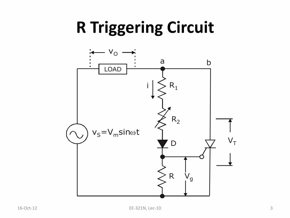
R Triggering Circuit
LOAD
vO
a b
i R1
R2
D
R Vg
VT
v =V sin tS m
16-Oct-12 3 EE-321N, Lec-10

R Triggering Ckt...contd
• Simplest triggering circuit
• Limited triggering angle range (0° to 90°)
• Performance depends upon temperature & SCR characteristics
• In the above fig. R1 is the current limiting resistor, R2 is the variable resistor which controls the firing angle and R is the stabilizing resistor
16-Oct-12 EE-321N, Lec-10 4
R Triggering Ckt...contd
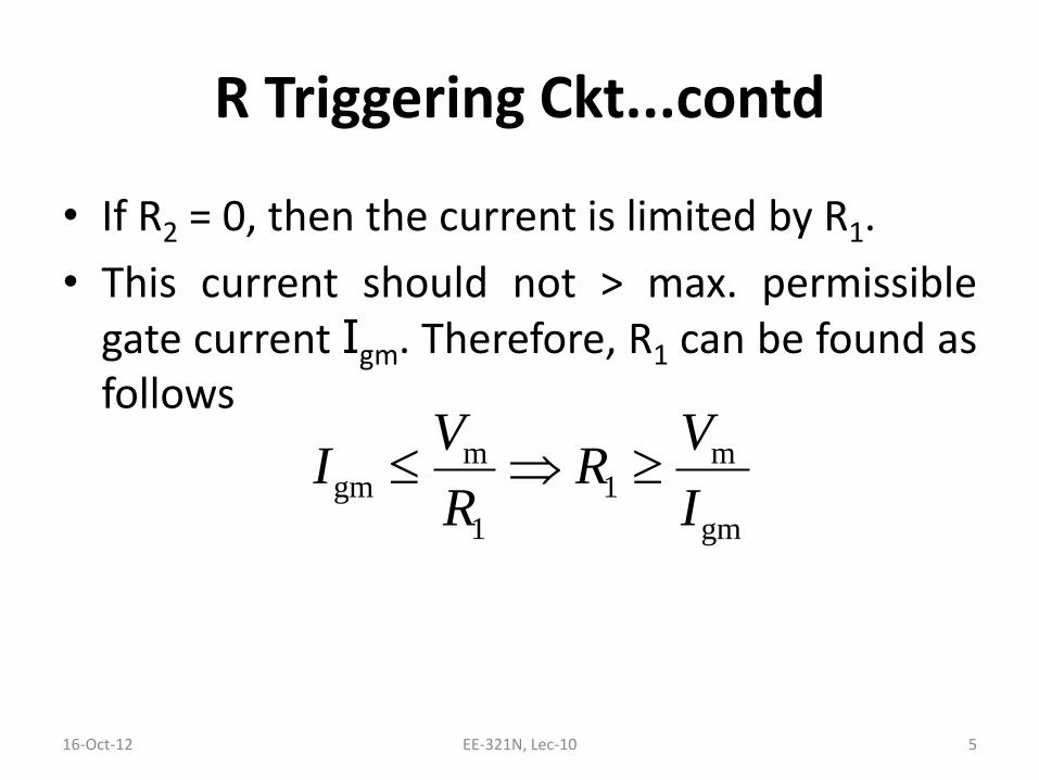
• If R2 = 0, then the current is limited by R1.
• This current should not > max. permissible gate current Igm. Therefore, R1 can be found as follows
16-Oct-12 EE-321N, Lec-10 5
m mgm 1
1 gm
V VI R
R I

R Triggering Ckt...contd
• R is chosen s. t. max. voltage across it doesn’t exceed max. forward gate voltage Vgm. Therefore,
16-Oct-12 EE-321N, Lec-10 6
gm 1m2
1 m gm
, 0gm
V RVR V R R
R R V V
R Triggering Ckt...contd
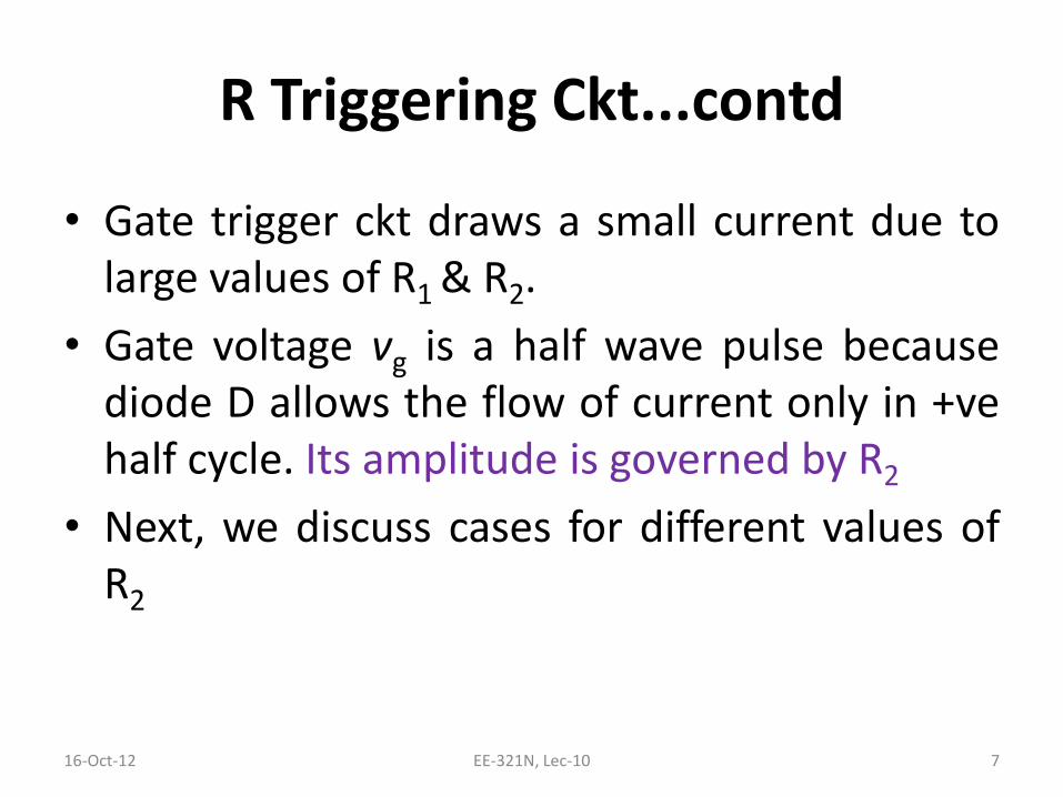
• Gate trigger ckt draws a small current due to large values of R1 & R2.
• Gate voltage vg is a half wave pulse because diode D allows the flow of current only in +ve half cycle. Its amplitude is governed by R2
• Next, we discuss cases for different values of R2
16-Oct-12 EE-321N, Lec-10 7
Case 1: R2 is large, No triggering
• When R2 is large, current i is small and voltage vg = iR is also small
• If peak value of gate voltage Vgp < VGT , SCR will not turn ON and accordingly there will be no O/P voltage or current and the supply voltage will appear ax the SCR
16-Oct-12 EE-321N, Lec-10 8

Case 2: α = 90°
• When R2 is decreased s. t. Vgp = VGT , α = 90° is obtained which can’t increase beyond this value
• This is because the thyristor latches into conduction as soon as Vgp becomes equal to VGT for the first time
16-Oct-12 EE-321N, Lec-10 9
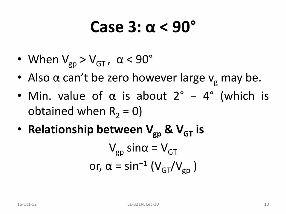
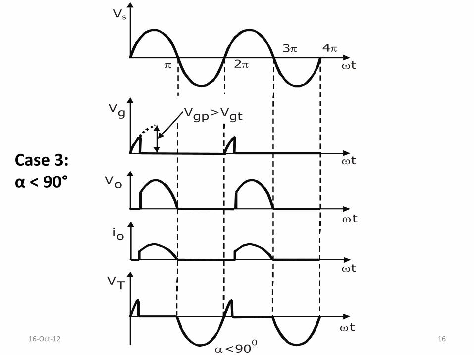
Case 3: α < 90°
• When Vgp > VGT , α < 90°
• Also α can’t be zero however large vg may be.
• Min. value of α is about 2° − 4° (which is obtained when R2 = 0)
• Relationship between Vgp & VGT is
Vgp sinα = VGT
or, α = sin−1 (VGT/Vgp )
16-Oct-12 EE-321N, Lec-10 10

Contd...
All other quantities except R2 are fixed. Hence firing angle is proportional to R2
16-Oct-12 EE-321N, Lec-10 11
mgp
1 2
GT 1 21
m
Since,
sin
V RV
R R R
V R R R
V R
Waveforms
16-Oct-12 12 EE-321N, Lec-10

Tip for Drawing Waveforms
• Use a graph paper or math notebook (with squares) to draw waveforms
• This will help you to remember (& draw fast in exam!) the waveforms easily
• Take 1 cm = 30° (on x-axis) & 2 cm = max. amp. of sine wave (on y-axis). Use different colors for showing different waves on same axis
16-Oct-12 13 EE-321N, Lec-10

VS
2
3 4
t
V sin tm
Vg Vgt
t
t
t
t
Vo
io
VT
VgpVgtVgp
R Large216-Oct-12 14
Case 1: No Triggering

16-Oct-12 15
t
t
t
t
t
2
3 4
VS
Vg
Vo
io
VT
V =Vgp gt
2700
2
3 4
900 =90
0
Case 2: α = 90°
t
t
t
t
t
2
3 4
VS
Vg
Vo
io
VT
<900
V >Vgp gt
16-Oct-12 16
Case 3: α < 90°
Related Documents