318 • 2007 IEEE International Solid-State Circuits Conference ISSCC 2007 / SESSION 17 / ANALOG TECHNIQUES AND PLLs / 17.9 17.9 A 62μA Interface ASIC for a Capacitive 3-Axis Micro-Accelerometer Matti Paavola 1 , Mika Kämäräinen 1 , Jere Järvinen 1 , Mikko Saukoski 1 , Mika Laiho 1,2 , Kari Halonen 1 1 Helsinki University of Technology, Espoo, Finland 2 University of Turku, Turku, Finland Capacitive accelerometers [1] have advantages such as zero stat- ic bias current, the capability of high sensitivity, and excellent thermal stability, making their use in low-power applications attractive. In this paper, an interface ASIC designed for a capac- itive 3-axis micro-accelerometer [2] is presented. The die area and power dissipation are reduced by using time-multiplexed sampling and duty cycles down to 0.3%. The block diagram of the interface with the sensor element [2] is shown in Fig. 17.9.1. The element is composed of four proof mass- es. The front-end converts the capacitive acceleration information to a voltage. Two algorithmic ADCs convert the acceleration and temperature information into the digital domain. These ADCs are powered down between their conversion cycles. The clock genera- tor provides a 2MHz system clock (SYSCLK), and a 1 to 50MHz microcontroller unit clock (MCUCLK). The latter makes possible more computationally intensive DSP if required. The bandgap- based voltage, current, and temperature reference (V/I/TREF) provides all reference voltages and currents and also tempera- ture information. To provide a more accurate and stable reference current, one off-chip resistor is needed. The operation is con- trolled by an off-chip DSP. To reduce the distorting effects of the electrostatic forces, a sin- gle-ended self-balancing bridge [3] was chosen as the starting point in the design of the front-end. The power dissipation and die area of the front-end (Fig. 17.9.2) are reduced by using time- multiplexing, thus making possible the reading of one, two, or four proof masses of the 3-axis accelerometer. The clock frequen- cy and biasing currents of the front-end are programmable. Chopper stabilization (CS) and CDS are implemented in order to reduce the offset voltage and noise of the front-end. The front-end controls the voltage of the middle electrode DMID; that is, when measuring at DC, the electrostatic forces are equal in the sensor capacitors CDP(n) and CDN(n), n being the index of the proof mass. The front-end can be used in both differential and single- ended modes. In differential mode, to convert single-ended sig- nals from the sensor element into differential form, the first amplifier is a differential difference amplifier (DDA), making pos- sible the more effective use of signal range in the ADC. The sin- gle-ended mode can be used to reduce power dissipation at the cost of reduced dynamic range. To minimize both power dissipation and silicon area, an algorith- mic capacitance ratio-independent ADC was chosen. The ADC architecture is insensitive to capacitance ratio, amplifier offset voltage, and flicker noise. It requires only one differential ampli- fier, a dynamic latch, 6 capacitors, 36 switches, and some digital logic. Thus, the active die area for a single ADC is only 0.04mm 2 . The structure also makes it possible to use asynchronous and time-multiplexed sampling, requiring only simple control logic. Furthermore, the duty-cycle of the ADC and the respective refer- ences is programmable so as to allow more flexible control of cur- rent consumption. The operating phases of the implemented ADCs are shown in Fig. 17.9.3. One bit polarity is resolved in four clock steps. The MSB is resolved in phases 1 to 4, and the rest of the bits are resolved by recycling phases 5 to 8. Thus, the total conversion cycle for a 12b operation is 48 clock steps. The operational amplifiers account for a major part of the current consumption in the front-end and the ADCs. To minimize power dissipation, the tail-current-boosted Class-AB operational ampli- fier [4] shown in Fig. 17.9.4 is used. The differential input pair M1-M2 is operated in weak inversion in order to maximize the current efficiency g m /I D . When the amplifier is used as a compara- tor in phases 4 and 8 in Fig. 17.9.3, tail-current boosting is dis- abled by replacing the dynamically controlled current sources M5-M6 with a static current source. When the ADC is powered down, the gates of M3-M8 are pulled to their respective supplies to turn off the transistors, and the common-mode feedback circuit is disabled. In the front-end, the same amplifier topology is used. When operated in differential mode, the DDA is implemented by adding another tail-current-boosted input pair to the normal dif- ferential amplifier. The SYSCLK is based on a source-coupled CMOS multivibrator, whose oscillation frequency is calibrated to 2MHz at room tem- perature using on-chip resistor and capacitor matrices. The MCUCLK, using a 1.2V supply, is a 3-stage single-ended current- starved ring oscillator with its oscillation frequency tunable from 1 to 50MHz. The V/I/TREF is based on Brokaw’s bandgap refer- ence [5]. The reference voltages of 1.2 and 0.9V are generated using two load resistors in series at the output stage of the feed- back amplifier. The current reference of 1µA is generated by using the 1.2V reference voltage and a 1.2MΩ off-chip resistor driven by an on-chip voltage buffer. The inherent PTAT voltage of the bandgap reference is exploited by the TREF. The buffered and amplified PTAT voltage is converted by the TREF ADC. Because the temperature changes slowly, a duty-cycle of 0.3% is used to reduce the current consumption of the TREF and the TREF ADC to negligible levels. The prototype was fabricated in a 0.13µm CMOS technology, using MIM capacitors and high-resistivity resistors. The active area of the chip (Fig. 17.9.7) is 0.51mm 2 . The chip was combined with an external ±4g capacitive 3-axis accelerometer on a PCB. The measured FFT plot for z-directional -1g acceleration is shown in Fig. 17.9.5. The measured noise densities in the x, y, and z directions with a 1kS/s sampling frequency are 460µg/√Hz, 550µg/√Hz, and 550µg/√Hz, respectively. These results yield a dynamic range of 65dB at the 100Hz bandwidth. The results are expected to improve when the interface is bonded directly to the sensor. Figure 17.9.5 also shows measured arbitrary accelera- tions in all three directions. The core of this sensor ASIC without the MCUCLK draws 62µA from a 1.8V supply while sampling temperature at 100S/s and four proof masses, each at 1kS/s. The overall performance is sum- marized in Fig. 17.9.6. Acknowledgments: We thank VTI Technologies for the sensor elements and funding; Nokia Research Center, and the Finnish Funding Agency for Technology and Innovation for funding. References: [1] M. Lemkin et al., “A 3-Axis Surface Micromachined Σ∆ Accelerometer,” ISSCC Dig. Tech. Papers, pp. 202-203, 1997. [2] T. Lehtonen and J. Thurau, “Monolithic Accelerometer for 3D Measurements,” Advanced Microsystems for Automotive Applications, pp. 11-22, J. Valldorf, W. Gessner Eds., Springer, 2004. [3] H. Leuthold and F. Rudolf, “An ASIC for High-Resolution Capacitive Microaccelerometers,” Sens. Actuators A, vol. 21, pp. 278–281, Feb., 1990. [4] R. Harjani, R. Heineke and F. Wang, “An Integrated Low-Voltage Class AB CMOS OTA,” IEEE J. Solid-State Circuits, pp. 134–142, Feb., 1999. [5] A. P. Brokaw, “ASimple Three-Terminal IC Bandgap Reference,” IEEE J. Solid-State Circuits, pp. 388–393, Dec., 1974. 1-4244-0852-0/07/$25.00 ©2007 IEEE.

Welcome message from author
This document is posted to help you gain knowledge. Please leave a comment to let me know what you think about it! Share it to your friends and learn new things together.
Transcript
318 • 2007 IEEE International Solid-State Circuits Conference
ISSCC 2007 / SESSION 17 / ANALOG TECHNIQUES AND PLLs / 17.9
17.9 A 62µµA Interface ASIC for a Capacitive 3-Axis Micro-Accelerometer
Matti Paavola1, Mika Kämäräinen1, Jere Järvinen1, Mikko Saukoski1,Mika Laiho1,2, Kari Halonen1
1Helsinki University of Technology, Espoo, Finland2University of Turku, Turku, Finland
Capacitive accelerometers [1] have advantages such as zero stat-ic bias current, the capability of high sensitivity, and excellentthermal stability, making their use in low-power applicationsattractive. In this paper, an interface ASIC designed for a capac-itive 3-axis micro-accelerometer [2] is presented. The die areaand power dissipation are reduced by using time-multiplexedsampling and duty cycles down to 0.3%.
The block diagram of the interface with the sensor element [2] isshown in Fig. 17.9.1. The element is composed of four proof mass-es. The front-end converts the capacitive acceleration informationto a voltage. Two algorithmic ADCs convert the acceleration andtemperature information into the digital domain. These ADCs arepowered down between their conversion cycles. The clock genera-tor provides a 2MHz system clock (SYSCLK), and a 1 to 50MHzmicrocontroller unit clock (MCUCLK). The latter makes possiblemore computationally intensive DSP if required. The bandgap-based voltage, current, and temperature reference (V/I/TREF)provides all reference voltages and currents and also tempera-ture information. To provide a more accurate and stable referencecurrent, one off-chip resistor is needed. The operation is con-trolled by an off-chip DSP.
To reduce the distorting effects of the electrostatic forces, a sin-gle-ended self-balancing bridge [3] was chosen as the startingpoint in the design of the front-end. The power dissipation anddie area of the front-end (Fig. 17.9.2) are reduced by using time-multiplexing, thus making possible the reading of one, two, orfour proof masses of the 3-axis accelerometer. The clock frequen-cy and biasing currents of the front-end are programmable.Chopper stabilization (CS) and CDS are implemented in order toreduce the offset voltage and noise of the front-end. The front-endcontrols the voltage of the middle electrode DMID; that is, whenmeasuring at DC, the electrostatic forces are equal in the sensorcapacitors CDP(n) and CDN(n), n being the index of the proofmass. The front-end can be used in both differential and single-ended modes. In differential mode, to convert single-ended sig-nals from the sensor element into differential form, the firstamplifier is a differential difference amplifier (DDA), making pos-sible the more effective use of signal range in the ADC. The sin-gle-ended mode can be used to reduce power dissipation at thecost of reduced dynamic range.
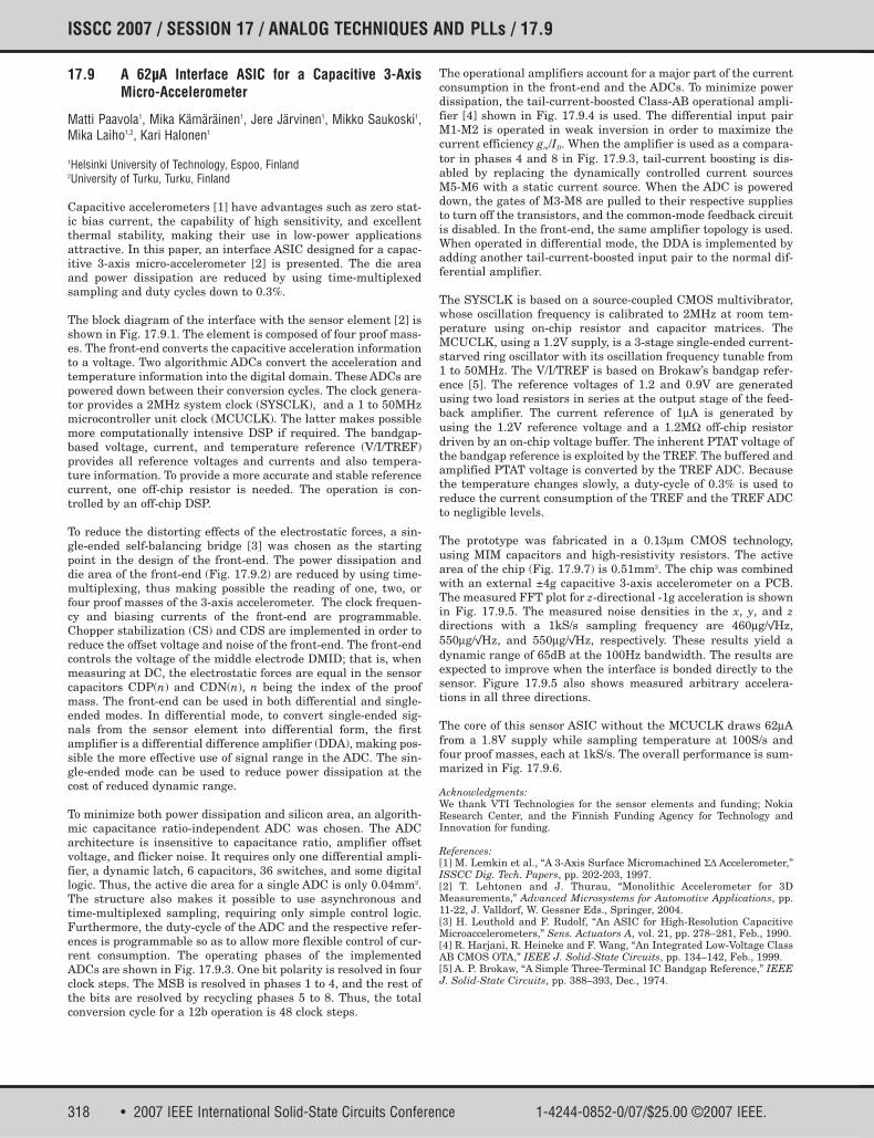
To minimize both power dissipation and silicon area, an algorith-mic capacitance ratio-independent ADC was chosen. The ADCarchitecture is insensitive to capacitance ratio, amplifier offsetvoltage, and flicker noise. It requires only one differential ampli-fier, a dynamic latch, 6 capacitors, 36 switches, and some digitallogic. Thus, the active die area for a single ADC is only 0.04mm2.The structure also makes it possible to use asynchronous andtime-multiplexed sampling, requiring only simple control logic.Furthermore, the duty-cycle of the ADC and the respective refer-ences is programmable so as to allow more flexible control of cur-rent consumption. The operating phases of the implementedADCs are shown in Fig. 17.9.3. One bit polarity is resolved in fourclock steps. The MSB is resolved in phases 1 to 4, and the rest ofthe bits are resolved by recycling phases 5 to 8. Thus, the totalconversion cycle for a 12b operation is 48 clock steps.
The operational amplifiers account for a major part of the currentconsumption in the front-end and the ADCs. To minimize powerdissipation, the tail-current-boosted Class-AB operational ampli-fier [4] shown in Fig. 17.9.4 is used. The differential input pairM1-M2 is operated in weak inversion in order to maximize thecurrent efficiency gm/ID. When the amplifier is used as a compara-tor in phases 4 and 8 in Fig. 17.9.3, tail-current boosting is dis-abled by replacing the dynamically controlled current sourcesM5-M6 with a static current source. When the ADC is powereddown, the gates of M3-M8 are pulled to their respective suppliesto turn off the transistors, and the common-mode feedback circuitis disabled. In the front-end, the same amplifier topology is used.When operated in differential mode, the DDA is implemented byadding another tail-current-boosted input pair to the normal dif-ferential amplifier.
The SYSCLK is based on a source-coupled CMOS multivibrator,whose oscillation frequency is calibrated to 2MHz at room tem-perature using on-chip resistor and capacitor matrices. TheMCUCLK, using a 1.2V supply, is a 3-stage single-ended current-starved ring oscillator with its oscillation frequency tunable from1 to 50MHz. The V/I/TREF is based on Brokaw’s bandgap refer-ence [5]. The reference voltages of 1.2 and 0.9V are generatedusing two load resistors in series at the output stage of the feed-back amplifier. The current reference of 1µA is generated byusing the 1.2V reference voltage and a 1.2MΩ off-chip resistordriven by an on-chip voltage buffer. The inherent PTAT voltage ofthe bandgap reference is exploited by the TREF. The buffered andamplified PTAT voltage is converted by the TREF ADC. Becausethe temperature changes slowly, a duty-cycle of 0.3% is used toreduce the current consumption of the TREF and the TREF ADCto negligible levels.
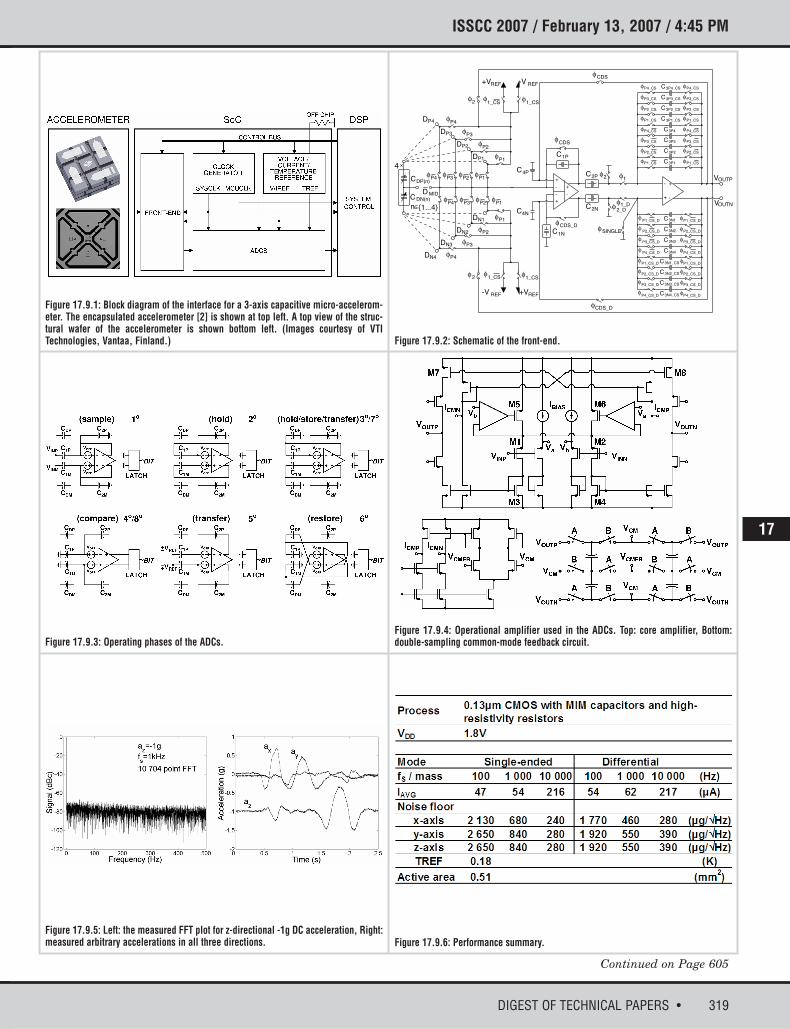
The prototype was fabricated in a 0.13µm CMOS technology,using MIM capacitors and high-resistivity resistors. The activearea of the chip (Fig. 17.9.7) is 0.51mm2. The chip was combinedwith an external ±4g capacitive 3-axis accelerometer on a PCB.The measured FFT plot for z-directional -1g acceleration is shownin Fig. 17.9.5. The measured noise densities in the x, y, and zdirections with a 1kS/s sampling frequency are 460µg/√Hz,550µg/√Hz, and 550µg/√Hz, respectively. These results yield adynamic range of 65dB at the 100Hz bandwidth. The results areexpected to improve when the interface is bonded directly to thesensor. Figure 17.9.5 also shows measured arbitrary accelera-tions in all three directions.
The core of this sensor ASIC without the MCUCLK draws 62µAfrom a 1.8V supply while sampling temperature at 100S/s andfour proof masses, each at 1kS/s. The overall performance is sum-marized in Fig. 17.9.6.
Acknowledgments:We thank VTI Technologies for the sensor elements and funding; NokiaResearch Center, and the Finnish Funding Agency for Technology andInnovation for funding.
References:[1] M. Lemkin et al., “A 3-Axis Surface Micromachined Σ∆ Accelerometer,”ISSCC Dig. Tech. Papers, pp. 202-203, 1997. [2] T. Lehtonen and J. Thurau, “Monolithic Accelerometer for 3DMeasurements,” Advanced Microsystems for Automotive Applications, pp.11-22, J. Valldorf, W. Gessner Eds., Springer, 2004.[3] H. Leuthold and F. Rudolf, “An ASIC for High-Resolution CapacitiveMicroaccelerometers,” Sens. Actuators A, vol. 21, pp. 278–281, Feb., 1990.[4] R. Harjani, R. Heineke and F. Wang, “An Integrated Low-Voltage ClassAB CMOS OTA,” IEEE J. Solid-State Circuits, pp. 134–142, Feb., 1999.[5] A. P. Brokaw, “A Simple Three-Terminal IC Bandgap Reference,” IEEEJ. Solid-State Circuits, pp. 388–393, Dec., 1974.
1-4244-0852-0/07/$25.00 ©2007 IEEE.
319DIGEST OF TECHNICAL PAPERS •
Continued on Page 605
ISSCC 2007 / February 13, 2007 / 4:45 PM
Figure 17.9.1: Block diagram of the interface for a 3-axis capacitive micro-accelerom-eter. The encapsulated accelerometer [2] is shown at top left. A top view of the struc-tural wafer of the accelerometer is shown bottom left. (Images courtesy of VTITechnologies, Vantaa, Finland.) Figure 17.9.2: Schematic of the front-end.
Figure 17.9.3: Operating phases of the ADCs.
Figure 17.9.5: Left: the measured FFT plot for z-directional -1g DC acceleration, Right:measured arbitrary accelerations in all three directions. Figure 17.9.6: Performance summary.
Figure 17.9.4: Operational amplifier used in the ADCs. Top: core amplifier, Bottom:double-sampling common-mode feedback circuit.
17

605 • 2007 IEEE International Solid-State Circuits Conference 1-4244-0852-0/07/$25.00 ©2007 IEEE.
ISSCC 2007 PAPER CONTINUATIONS
Figure 17.9.7: Chip micrograph.
Related Documents