• iSBC® 80/24A SINGLE BOARD COMPUTER HARDWARE REFERENCE MANUAL • Order Number: 148437-001 • r ."" • THE GREEN PAGES AT THE END OF THIS MANUAL CONTAIN ERRATA. IF NOGREEN PAGES ARE PRESENT, THIS MANUAL HAD NO ERRATA AT PRESS TIME. , :/ • Copyright 1985, Intel Corporation, All Rights Reserved I Intel Corporation, 3065 Bowers Avenue, Santa Clara, California 95051 I

Welcome message from author
This document is posted to help you gain knowledge. Please leave a comment to let me know what you think about it! Share it to your friends and learn new things together.
Transcript

• iSBC® 80/24A
SINGLE BOARD COMPUTER HARDWARE REFERENCE MANUAL
• Order Number: 148437-001
• r .""
• THE GREEN PAGES AT THE END OF THIS MANUAL CONTAIN ERRATA. IF NOGREEN
PAGES ARE PRESENT, THIS MANUAL HAD NO ERRATA AT PRESS TIME. , :/
• Copyright 1985, Intel Corporation, All Rights Reserved
I Intel Corporation, 3065 Bowers Avenue, Santa Clara, California 95051 I

ii
REV. REVISION HISTORY
-001 Original Issue.
Additional copies of this manual or other Intel literature may be obtained from:
Literature Department Intel Corporation 3065 Bowers Avenue Santa Clara, CA 95051
The information in this document is subject to change without notice.
DATE
11/85
Intel Corporation makes no warranty of any kind with regard to this material, including, but not limited to, the implied warranties of merchantability and fitness for a particular purpose. Intel Corporation assumes no responsibility for any errors that may appear in this document. Intel Corporation makes no commitment to update nor to keep current the information contained in this document.
Intel Corporation assumes no responsibility for the use of any circuitry other than circuitry embodied in an Intel product. No other circuit patent licenses are implied.
Intel software products are copyrighted by and shall remain the property of Intel Corporation. Use, duplication or disclosure is subject to restrictions stated in Intel's software license, or as defined in ASPR 7-104.9(a)(9).
No part of this document may be copied or reproduced in any form or by any means without prior written consent of Intel Corporation.
Intel Corporation makes no warranty for the use of its products and assumes no responsibility for any errors which may appear in this document nor does it make a commitment to update the information contained herein.
Intel retains the right to make changes to these specifications at any time, without notice.
Contact your local sales office to obtain the latest specifications before placing your order.
The following are trademarks ofIntel Corporation and its affiliates and may be used only to identify Intel products:
Above iLBX iPDS ONCE BITBUS im iPSC OpenNET COMMputer iMDDX iRMX Plug-A-Bubble CREDIT iMMX iSBC PROMPT Data Pipeline Insite iSBX Promware GENIUS Intel iSDM QueX A intel iSXM QUEST i i intelBOS Library Manager Ripplemode I2ICE Intelevision MCS RMX/80 ICE inteligent Identifier Megachassis RUPI iCEL inteligent Programming MICROMAINFRAME Seamless iCS Intellec MULTIBUS SLD iDBP Intellink MULTICHANNEL UPI iDIS iOSP MULTIMODULE VLSiCEL
MDS is an ordering code only and is not used as a product name or trademark. MDS® is a registered trademark of Mohawk Data Sciences Corporation.
*MULTIBUS is a patented Intel bus.
Copyright 1985, Intel Corporation, All Rights Reserved
•
•
•
•
•

•
•
•
•
•
PREFACE I
This manual provides general information, installation and setup instructions, programming guidelines for the on-board devices, board level principles of operation, and repair and replacement assistance information for the iSBC 80/24A Single Board Computer. Related information is provided in the following documents:
• Intel MUmBUS Specification, Order Number 9800683.
• Intel MULTIBUS Interfacing, Application Note AP-28A.
• Intel Microsystems Component Handbook, Order Number 230843.
• Using the 8259A Programmable Interrupt Controller, Application Note AP-59.
• Intel Memory Components Handbook, Order Number 210830.
• Intel's 5V EPROM/ROM Family, Application Note AP-30.
• Intel MCS-80/85 Family User's Manual, Order Number 205775 .
• Intel RMX/80 User's Guide, Order Number 9800522.
• Intel iSBC 604/614 Cardcage Hardware Reference Manual, Order Number 9800708.
• Intel iSBC 655 System Chassis Hardware Reference Manual, Order Number 9800709.
• Intel iSBC 660 System Chassis Hardware Reference Manual, Order Number 9800505.
• Intel iSBX 331 Fixed/Floating Point Math MULTIMODULE Board Hardware Reference Manual, Order Number 142668.
• Intel iSBX 344 Intelligent BITBUSTM Interface Board User's Guide, Order Number 148009.
• Intel iSBX 350 Parallel I/O MULTIMODULE Board Hardware Reference Manual, Order Number 9803191.
• Intel iSBX 351 Serial I/O MULTIMODULE Board Hardware Reference Manual, Order Number 9803190.
iiiliv

•
•
•
•
•

•
•
•
•
•
NOTE TO READERS:
This hardware reference manual utilizes a visual scheme to denote section levels, rather than a numerical scheme used in many technical documents. This visual scheme allows you to more readily identify which section headings are subsections. Therefore, each section will have the same numbering convention throughout the manual (i.e., section 1-3, section 2-20, section 4-32). The visual distinction among the different sizes and fn.e different fonts used for section headings indicate what level or order a particular section occupies. The following example illustrates how this system is used in this manual:
3-27. 8259A PIC PROGRAMMING
3-28. INTERRUPT PRIORITY MODES
3-29. FULLY NESTED MODE. In this ...
1st Order Heading
2nd Order Heading
3rd Order Heading
By glancing through this manual before you start reading, the visual method of section ordering will become apparent. You may also refer to the Table of Contents on page vii, to see how the sections compare to each other.
v/vi

•
•
•
•
•
•
•
•
•
•
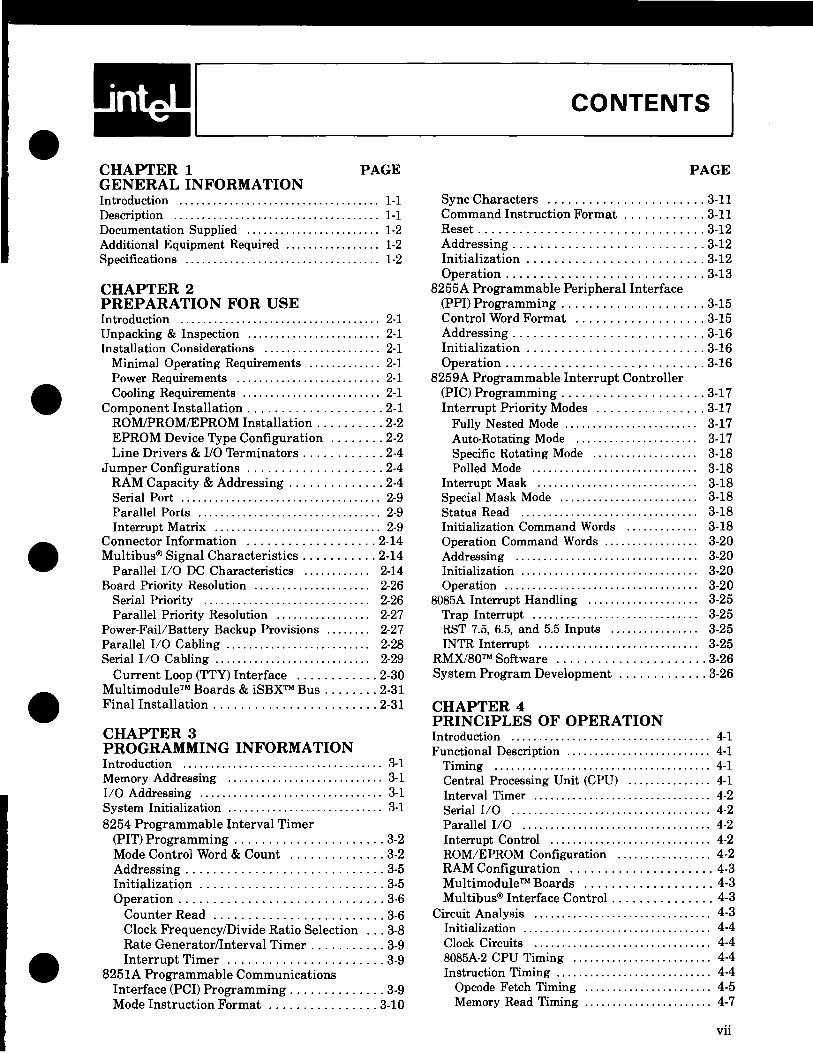
CHAPTER 1 PAGE GENERAL INFORMATION Introduction .................................... 1-1 Description ..................................... 1-1 Documentation Supplied ........................ 1-2 Additional Equipment Required ................. 1-2 Specifications ................................... 1-2
CHAPTER 2 PREPARATION FOR USE Introduction .................................... 2-1 Unpacking & Inspection ........................ 2-1 Installation Considerations ..................... 2-1
Minimal Operating Requirements ............. 2-1 Power Requirements .......................... 2-1 Cooling Requirements ......................... 2-1
Component Installation .................... 2-1 ROMIPROMIEPROM Installation .......... 2-2 EPROM Device Type Configuration ........ 2-2 Line Drivers & I/O Terminators ............ 2-4
Jumper Configurations .................... 2-4 RAM Capacity & Addressing .............. 2-4 Serial Port .................................... 2-9 Parallel Ports ................................. 2-9 Interrupt Matrix .............................. 2-9
Connector Information ................... 2-14 Multibus® Signal Characteristics ........... 2-14
Parallel I/O DC Characteristics ............ 2-14 Board Priority Resolution ..................... 2-26
Serial Priority .............................. 2-26 Parallel Priority Resolution ................. 2-27
Power·Fail/Battery Backup Provisions ........ 2-27 Parallel I/O Cabling .......................... 2-28 Serial I/O Cabling............................ 2-29
Current Loop (TTY) Interface ............ 2-30 Multimodule™ Boards & iSBXTM Bus ........ 2-31 Final Installation ........................ 2-31
CHAPTER 3 PROGRAMMING INFORMATION Introduction .................................... 3-1 Memory Addressing ............................ 3-1 I/O Addressing ................................. 3-1 System Initialization ............................ 3-1 8254 Programmable Interval Timer
(PIT) Programming ...................... 3-2 Mode Control Word & Count .............. 3-2 Addressing . . . . . . . . . . . . . . . . . . . . . . . . . . . . . 3-5 Initialization ........................... 3-5 Operation .............................. 3-6
Counter Read ......................... 3-6 Clock Frequency/Divide Ratio Selection ... 3-8 Rate GeneratorlInterval Timer ........... 3-9 Interrupt Timer ....................... 3-9
8251A Programmable Communications Interface (PCl) Programming .............. 3-9 Mode Instruction Format ................ 3-10
CONTENTS
PAGE
Sync Characters ....................... 3-11 Command Instruction Format ............ 3-11 Reset ................................. 3-12 Addressing ............................ 3-12 Initialization .......................... 3-12 Operation ............................. 3-13
8255A Programmable Peripheral Interface (PPl) Programming ..................... 3-15 Control Word Format ................... 3-15 Addressing ............................ 3-16 Initialization .......................... 3-16 Operation ............................. 3-16
8259A Programmable Interrupt Controller (PIC) Programming ..................... 3-17 Interrupt Priority Modes ................ 3-17
Fully Nested Mode...... .. .. ... .. ...... ... 3-17 Auto·Rotating Mode ...................... 3-17 Specific Rotating Mode ................... 3-18 Polled Mode .............................. 3-18
Interrupt Mask ............................. 3-18 Special Mask Mode ......................... 3-18 Status Read ................................ 3-18 Initialization Command Words ............. 3-18 Operation Command Words................. 3-20 Addressing ................................. 3-20 Initialization ................................ 3-20 Operation ................................... 3-20
8085A Interrupt Handling .................... 3-25 Trap Interrupt .............................. 3-25 RST 7.5, 6.5, and 5.5 Inputs ................ 3-25 INTR Interrupt ............................. 3-25
RMX/80™ Software ...................... 3-26 System Program Development ............. 3-26
CHAPTER 4 PRINCIPLES OF OPERATION Introduction .................................... 4-1 Functional Description .......................... 4-1
Timing ....................................... 4-1 Central Processing Unit (CPU) ............... 4-1 Interval Timer ................................ 4-2 Serial I/O .................................... 4-2 Parallel 1/0 .................................. 4-2 Interrupt Control ............................. 4-2 ROMIEPROM Configuration ................. 4-2 RAM Configuration ..................... 4-3 Multimodule™ Boards ................... 4-3 Multibus® Interface Control ............... 4-3
Circuit Analysis ................................ 4-3 Initialization .................................. 4-4 Clock Circuits ................................ 4-4 8085A-2 CPU Timing ......................... 4-4 Instruction Timing ............................ 4-4
Opcode Fetch Timing ....................... 4-5 Memory Read Timing ....................... 4-7
vii

PAGE I/O Read Timing ........................... 4-7 Memory Write Timing ...................... 4-7 I/O Write Timing ........................... 4-8 Interrupt Acknowledge Timing .............. 4-8
Address Bus ................................. .4-10 Bus Time-Out ................................. 4-10 Data Bus ..................................... 4-10 Read/Write Signal Generation ................ 4-10 I/O Control Signals .......................... 4-10 Memory Control Signals ...................... 4-10 110 Operation .............................. 4-11 On·Board I/O Operation .................... 4-11 Off-Board I/O Operation .................... 4-11 Multibus® Interface .................... 4-11 Multibus® Override Feature .............. 4-12 Failsafe Timer .............................. 4-12 Interrupt Operation ......................... 4-12
Conclusion .................................... 4-13
CONTENTS (Continued)
CHAPTER 5 SERVICE AND REPAIR INFORMATION
PAGE
Introduction ............................. 5-1 Service & Repair Assistance ................ 5-1 Service Diagrams ......................... 5-1 Internal Signals .......................... 5-3
APPENDIX A 8085A INSTRUCTION SET
APPENDIXB DECODE PROM (U32)
APPENDIXC iSBC 80/20-4 BOARD; iSBC 80/24 BOARD; iSBC 80/24A BOARD FUNCTIONAL DIFFERENCES
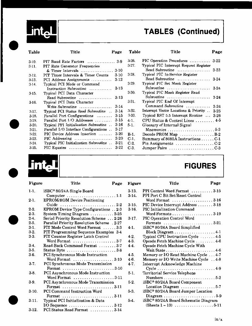
TABLES
Table Title Page Table Title Page
1·1. 2-1. 2-2. 2-3. 2-4. 2-4A. 2-5. 2-6.
2-7.
2-8. 2-9. 2-10. 2-11. 2-12. 2-13. 2-14. 2-15. 2-16.
viii
Specifications ..................... 1-2 EPROMIROM Configurations ........ 2-2 Wait State Jumpers ................ 2-3 Recommended I/O Terminators ....... 2-4 Jumper Connections ................ 2-4 Numerical Listing of Jumpers ....... 2-7 Serial Port Jumper Options .......... 2-9 Configuration Jumpers for Parallel
Ports E4 - EA ................... 2-10 Interrupt Matrix Jumper
Connections .................... 2-15 User Furnished Connector Details ... 2-16 Connector PI Pin Assignments ...... 2-17 Connector PI Signal Definitions ..... 2-18 Connector P2 Pin Assignments ...... 2-19 Connector P2 Signal Definitions ..... 2-19 AC Characteristics at 4.84 MHz ..... 2-20 AC Characteristics at 2.42 MHz ..... 2-21 DC Characteristics (PI Signals) ..... 2-22 DC Characteristics (P2 Signals) ..... 2-24
2-17. DC Characteristics (J1 & J2 Parallel 110 Ports) ................. 2-24
2-18. Connector J1 Pin Assignments 2-29 2-19. Connector J2 Pin Assignments 2-29 2-20. Connector J3 Pin Assignments 2-30 2-21. Connector Pin Correspondence
(25-Pin to 26-Pin) ................... 2-30 2-22. iSBXTM Bus Connector Pin
Assignments ....................... 2-31 2-22A. iSBXTM Bus Signal Descriptions ...... 2-31 3-1. EPROM/ROM Memory Size ............ 3-1 3-2. On-Board RAM Address
Space (Hexadecimal) ................. 3-1 3-3. I/O Port Addressing ................... 3-2 3-4. PIT Counter Operation Vs. Gate Inputs . 3-5 3-5. PIT Register Addresses ................ 3-5 3-6. Typical PIT Control Word .... " ........ 3-6 3-7. PIT Control Word & Count Loading ... 3-6 3-8. Typical PIT Counter Read Subroutine .. 3-7 3-9. PIT Count Values & Rate Multipliers .. 3-9
•
•
•
•
•
•
•
•
•
•
Table
3-10. 3-11.
3-12_ 3-13_ 3-14.
3-15.
3-16.
3-17. 3-18. 3-19 . 3-20. 3-21. 3-22. 3-23. 3-24. 3-25.
Figure
1-1.
2-1.
2-2. 2-3. 2-4. 2-5. 3-1. 3-2. 3-3.
3-4. 3-5. 3-6.
3-7.
3-8.
3-9.
3-10.
3-11.
3-12.
Title Page
PIT Baud Rate Factors ......... . . . . . .. 3-9 PIT Rate Generator Frequencies
& Timer Intervals ................... 3-10 PIT Timer Intervals & Timer Counts 3-10 PCI Address Assignments............ 3-12 Typical PCI Mode or Command
Instruction Subroutine ............. 3-13 Typical PCI Data Character
Read Subroutine ................... 3-13 Typical PCI Data Character
Write Subroutine ................... 3-14 Typical PCI Status Read Subroutine .. 3-14 Parallel Port Configurations ......... 3-15 Parallel Port I/O Addresses .......... 3-15 Typical PPI Initialization Subroutine .. 3-16 Parallel I/O Interface Configurations .. 3-17 PIC Device Address Insertion ........ 3-20 PIC Addressing ...................... 3-20 Typical PIC Initialization Subroutine .. 3-21 PIC Equates ......................... 3-22
Table
3-26. 3-27.
3-28.
3-29.
3-30.
3-31.
3-32. 3-33. 4-1. 5-1.
B-l. C-l. C-2. C-3.
Title Page Figure
iSBC® 80/24A Single Board Computer ....................... 1-1
EPROMIROM Device Positioning Guide .......................... 2-2
EPROM Device Type Configurations .. 2-3 System Timing Diagram ........... 2-25 Serial Priority Resolution Scheme ... 2-26 Parallel Priority Resolution Scheme .2-27 PIT Mode Control Word Format ...... 3-3 PIT Programming Sequence Examples 3-4 PIT Counter Register Latch Control
Word Format .................... 3-7 Read-Back Command Format ........ 3-7 Status Byte ....................... 3-8 PCI Synchronous Mode Instruction
Word Format ................... 3-10 PCI Synchronous Mode Transmission
Format ........................ 3-10 PCI Asynchronous Mode Instruction
Word Format ................... 3-11 PCI Asynchronous Mode Transmission
Format ........................ 3-11 PCI Command Instruction Word
Format ........................ 3-11 Typical PCI Initialization & Data VO Sequence ..................... 3-12 PCI Status Read Format ........... 3-14
3-13. 3-14.
3-15. 3-16.
3-17.
4-1.
4-2. 4-3. 4-4.
4-5. 4-6. 4-7.
5-1.
5-2.
5-3.
5-4.
TABLES (Continued)
Title Page
PIC Operation Procedures ............ 3-22 Typical PIC Interrupt Request Register
Read Subroutine ................... 3·23 Typical PIC In-Service Register
Read Subroutine ................... 3-24 Typical PIC Set Mask Register
Subroutine ......................... 3-24 Typical PIC Mask Register Read
Subroutine ......................... 3-24 Typical PIC End Of Interrupt
Command Subroutine .............. 3-24 Interrupt Vector Locations & Priority .. 3-25 Typical RST 5.5 Interrupt Routine .,. 3-26 CPU Status & Control Lines ......... 4-5 Glossary of Internal Signal
Mnemonics ...................... 5-3 Decode PROM Map ................ B-2 Summary of 8085A Instructions ...... C-1 Pin Assignments .................. C-2 Jumper Pairs ..................... C-3
FIGURES
Title Page
PPI Control Word Format .......... 3-15 PPI Port C Bit SetlReset Control
Word Format ................... 3-16 PIC Device Interrupt Address ....... 3-18 PIC Initialization Command
Word Formats ................... 3-19 PIC Operation Control Word
Formats ....................... 3-21 iSBC® 80/24A Board Simplified
Block Diagram ................... 4-1 Typical CPU Instruction Cycle ....... 4-5 Opcode Fetch Machine Cycle ......... 4-6 Opcode Fetch Machine Cycle With
Wait State ....................... 4-6 Memory or VO Read Machine Cycle ... 4-7 Memory or 1/0 Write Machine Cycle .. 4-8 Interrupt Acknowledge Machine
Cycle ........................... 4-9 Territorial Service Telephone
Numbers ........................ 5-2 iSBC® 80/24A Board Component
Location Diagram ................ 5-7 iSBC® 80/24A Board Jumper Location
Diagram ........................ 5-9 iSBC® 80/24A Board Schematic Diagram
(Sheets 1 - 10) .................. 5-11
ix/x

•
•
•
•
•

•
•
•
•
•
1-1. INTRODUCTION
The iSBC SO/24A Single Board Computer is a Multibus and Multimodule compatible computer system on a single printed circuit assembly (figure 1-1). The iSBC SO/24A board includes an Intel SOS5A-2 microprocessor, SK bytes of on-board random access memory (RAM), sockets for up to 32K bytes of on-board read-only memory (ROM), six programmable S-bit 110 ports, one programmable serial communications channel, a programmable interval timer, a programmable interrupt controller, and advanced bus controller circuitry .
This manual provides the information you will need to promptly install and operate the iSBC SO/24A board. To optimize your application of this flexible board, we suggest reading the entire manual before attempting installation and operation.
1-2. DESCRIPTION
The iSBC SO/24A board is controlled by an Intel SOS5A-2 microprocessor operating at 4.S4 MHz. System access is provided by the Multibus
CHAPTER 1 GENERAL INFORMATION
connector and an auxiliary connector. Off-board peripheral 110 operations are handled through 4S parallel lines, a serial communications channel connector and two iSBX Multimodule connectors.
The iSBC SO/24A board can directly access up to 64K bytes of memory. A single SRAM device supplies SK bytes of on-board RAM. Also, the board can accept up to 32K bytes of user-installed ROM, PROM, or EPROM devices (either 24- or 2S-pin devices as defined in Chapter 2).
The on-board S254 Programmable Interval Timer (PIT) provides three independent counter outputs which may be configured to a variety of applications, including frequency output, rate generator, interval timer and real-time interrupts. One of these counters serves as the baud rate clock for the on-board S251A Programmable Communications Interface (PC I) device.
Serial 110 operation is handled by an Intel S251A Programmable Communications Interface (PCI) device. The board is configured to the RS232C structure; however, it may be adapted to a TTY interface using optional equipment. Baud rates are software programmable via the on-board timer.
J1 PARALLEL 1/0 J2 PARALLEL I/O J3 SERIAL I/O
P1 MULTIBUS" CONNECTOR P2 AUXILIARY CONNECTOR
Figure 1-1. iSBC® 80/24A Single Board Computer
1-1

General Information
The iSBC 80/24A board utilizes two Intel 8255A Programmable Peripheral Interface (PPD devices to control the six, 8-bit parallel 110 ports. These ports may be configured to a variety of dedicated or general purpose applications. Two Intel 8287 Bus Transceiver devices are supplied for two of the ports and sockets for line driver or terminator devices are provided for the other four ports.
Up to eight interrupts are controlled by the 8259A Programmable Interrupt Controller (PIC), while four additional interrupts are handled directly by the 8085A-2 CPU. An interrupt jumper matrix allows the interrupt structure to be easily configured to your application.
Two iSBX bus connectors are provided on the iSBC 80/24A board. These connectors are designed to expand the board's 110 functions, using special purpose add-on Multimodule boards, such as the iSBX 344 Intelligent BITBUSTM Interface Board. One or two iSBX Multimodule boards may be added, as required by your application.
The iSBC 80/24A board is designed to operate as a full master in any Intel Multibus compatible chassis. The board may also reside in your own custom
iSBC80/24A
designed chassis, using Multibus compatible connectors (refer to Chapter 2).
1-3. DOCUMENTATION SUPPLIED
Each iSBC 80/24A board is shipped with a current set of schematic diagrams. Refer to Chapter 5 for related information.
1-4. ADDITIONAL EQUIPMENT REQUIRED
The iSBC 80/24A board requires few optional components for operation. Depending on your application, you may need to purchase up to three 110 connectors and cables. Anyon-board ROMIPROM must also be purchased separately. Chapter 2 provides information for selecting these items, based on your specific needs.
1-5. SPECIFICATIONS
Specifications of the iSBC 80/24A board are provided in table 1-1.
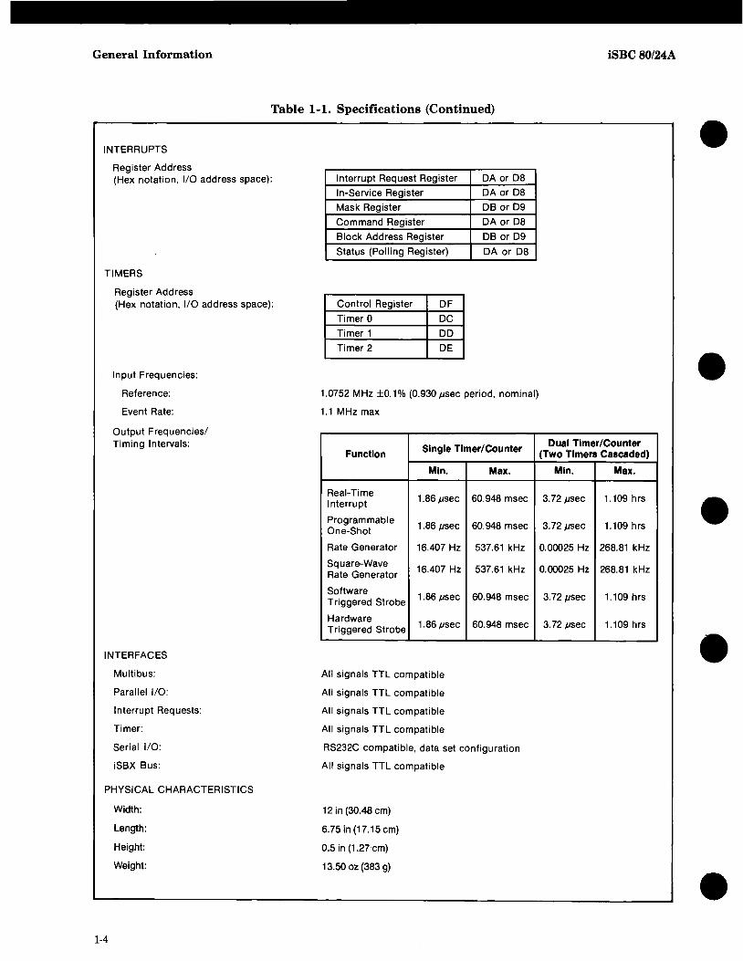
Table 1·1. Specifications
1-2
CPU
Operating Rate:
Single Clock Cycle:
Intel 8085A-2
4.84 MHz (default) 2.42 MHz (optional)
206 ns (at 4.84 MHz)
Basic Instruction Cycle (four clock cycles): 824 ns
WORD SIZE
Instruction:
Data:
Address:
SYSTEM CLOCK:
RAM ACCESS TIME:
MEMORY ADDRESSING (factory configuration)
On-Board ROM/EPROM:
On-Board RAM:
8, 16, or 24 bits
8 bits
16 bits
9.68 MHz
70 ns maximum (Valid data out from READ command)
0-7FFFH
EOOO-FFFFH
•
•
•
•
•

•
•
•
•
•
iSBC 80/24A
MEMORY CAPACITY
On-Board ROM/EPROM:
On-Board RAM:
Off-Board Expansion:
1/0 ADDRESSING
On-Board Programmable 1/0:
Optional:
ON-BOARD 1/0 CAPACITY
Parallel:
Serial:
SERIAL COMMUNICATIONS CHARACTERISTICS
Synchronous:
Asynchronous:
SERIAL BAUD RATES:
General Information
Table 1-1. Specifications (Continued)
Up to 32K bytes (user-installed)
8K bytes
Up to 64K bytes in combinations of RAM, ROM, and EPROM.
Note: ROMIEPROM may be added in 1 K, 2K, 4K, or 8K byte increments.
8255 No.1 8255 No.2 8255 8255 8251 8251 Port No.1 No.2 1 2 3 4 5 6 Control Control Data Control
Address E4 E5 E6 E8 E9 EA E7 EB EC ED
J5 Multlmodule J6 Multlmodule
i Co-CF FO-FF
48 programmable lines.
1 Transmit; 1 Receive; 1 SID; 1 SOD
Note: Expandable with Optional Multimodule boards
5-8 bit characters Internal or external character synchronization Automatic Sync Insertion
5-8 bit characters Break character generation 1, 1'/2, or 2 stop bits False start bit detectors
Output Baud Rate (Hz) Frequency
In kHz Synchronous Asynchronous
-;-16 -;-64
153.6 - 9600 2400
76.8 - 4800 1200
38.4 38400 2400 600
19.2 19200 1200 300
9.6 9600 600 150
4.8 4800 300 75
2.4 2400 150 -
1.76 1760 110 -
Baud Rate Register DE
8254 PIT Baud Rate Factor
(Hex Notation)
MSB LSB
00 07
00 OE
00 1C
00 38
00 70
00 EO
01 CO
02 63
Note: Baud Rate Factor (16 bits) is loaded as two sequential output operations to same address (DE) .
1-3
General Information
Table 1-1. Specifications (Continued)
INTERRUPTS
Register Address (Hex notation, liD address space):
TIMERS
Register Address (Hex notation, liD address space):
Input Frequencies:
Reference:
Event Rate:
Output Frequenciesl Timing Intervals:
INTERFACES
Multibus:
Parallel liD:
Interrupt Requests:
Timer:
Serial I/O:
iSBX Bus:
PHYSICAL CHARACTERISTICS
Width:
Length:
Height:
Weight:
1-4
Interrupt Request Register DA or D8
In-Service Register DA or D8
Mask Register DB or D9
Command Register DA or D8
Block Address Register DB or D9
Status (Polling Register) DA or D8
Control Register DF
Timer 0 DC
Timer 1 DD Timer 2 DE
1.0752 MHz ±0.1% (0.930 Jlsec period, nominal)
1.1 MHz max
Function Single Timer/Counter
Min.
Real-Time 1.86 Jlsec Interrupt
Programmable 1.86 Jlsec One-Shot
Rate Generator 16.407 Hz
Square-Wave 16.407 Hz Rate Generator
Software 1.86 Jlsec Triggered Strobe
Hardware 1.86 Jlsec Triggered Strobe
All signals TTL compatible
All signals TTL compatible
All signals TTL compatible
All signals TTL compatible
Max.
60.948 msec
60.948 msec
537.61 kHz
537.61 kHz
60.948 msec
60.948 msec
RS232C compatible, data set configuration
All signals TTL compatible
12 in (30.48 cm)
6.75 in (17.15 cm)
0.5 in (1.27cm)
13.50 oz (383 g)
iSBC 80/24A
•
• Dual Timer/Counter
(Two Timers Cascaded)
Min. Max.
3.72 Jlsec 1.109 hrs
3.72 Jlsec 1.109 hrs • 0.00025 Hz 268.81 kHz
0.00025 Hz 268.81 kHz
3.72 Jlsec 1.109 hrs
3.72 Jlsec 1.109hrs
•
•
•
•
•
•
•
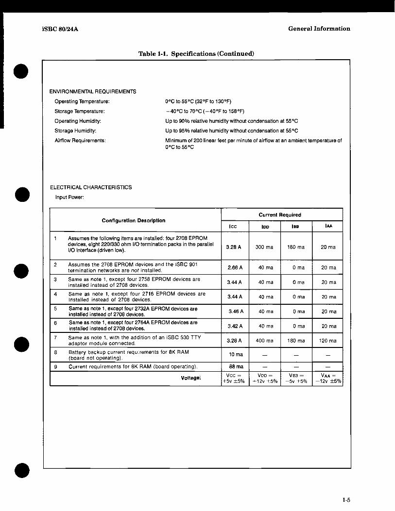
iSBC80/24A General Information
ENVIRONMENTAL REQUIREMENTS
Operating Temperature:
Storage Temperature:
Operating Humidity:
Storage Humidity:
Table 1·1. Specifications (Continued)
OOC to 55°C (32°F to 130°F)
-40°C to 70°C (-40°F to 158°F)
Up to 90% relative humidity without condensation at 55°C
Up to 95% relative humidity without condensation at 55°C
Airflow Requirements: Minimum of 200 linear feet per minute of airflow at an ambient temperature of OOC to 55°C
ELECTRICAL CHARACTERISTICS
Input Power:
Configuration Description
1 Assumes the following items are installed: four 2708 EPROM devices, eight 220/330 ohm 1/0 termination packs in the parallel 1/0 interface (driven low).
2 Assumes the 2708 EPROM devices and the iSBC 901 termination networks are not installed.
3 Same as note 1, except four 2758 EPROM devices are installed instead of 2708 devices.
4 Same as note 1, except four 2716 EPROM devices are installed instead of 2708 devices.
5 Same as note 1, except four 2732A EPROM devices are installed instead of 2708 devices.
6 Same as note 1, except four 2764A EPROM devices are installed instead of 2708 devices.
7 Same as note 1, with the addition of an iSBC 530 TTY adaptor module connected.
8 Battery backup current requirements for 8K RAM (board not operating).
9 Current requirements for 8K RAM (board operating).
Voltage:
Icc
3.28 A
2.66 A
3.44 A
3.44 A
3.46 A
3.42 A
3.28 A
10ma
88 rna
Vee = +5v ±5%
Current Required
IDD IBB 1M
300 rna 180 rna 20 rna
40 rna o rna 20 rna
40 rna o rna 20 rna
40 rna o rna 20 rna
40 rna o rna 20 rna
40 rna o rna 20 rna
400 rna 180 rna 120 rna
- - -
- - -Voo = VBB = VAA =
+12v ±5% -5v ±5% -12v ±5%
1-5
General Information iSBC 80/24A
Table 1·1. Specifications (Continued)
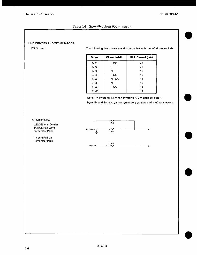
• LINE DRIVERS AND TERMINATORS
I/O Drivers: The following line drivers are all compatible with the I/O driver sockets.
Driver Characteristic Sink Current (mA)
7438 I,OC 48
7437 I 48
7432 NI 16
7426 I,OC 16
7409 NI,OC 16
7408 NI 16
7403 I,OC 16
7400 I 16
Note: I = inverting; NI = non-inverting; OC = open coliectoL • Ports E4 and E8 have 25 mA totem-pole dividers and 1 kCl terminators.
I/O Terminators: +5 : 1 220/330 ohm Divider Pull Up/Pull Down
220 1!l330!! J 0 Terminator Pack 330li • 1kohm Pull Up Terminator Pack
1kU
1 k 11 +5 ~ 0
•
• * * * 1-6

•
•
•
•
•
2-1. INTRODUCTION
This chapter provides specific information enabling you to install the iSBC 80/24A board into your own system, with minimal effort. The board's default, or factory configuration for RAM addressing, ROM type, and other variables is described, followed by procedures for altering the default configuration. In this manner, the board will accommodate a variety of applications. To completely familiarize yourself with the f1exibility of the iSBC 80/24A board, we recommend reading the entire chapter before installation and use.
2-2. UNPACKING AND INSPECTION
Inspect the shipping carton immediately upon receipt for evidence of mishandling during transit. If the shipping carton is severely damaged or waterstained, request that the carrier's agent be present when the carton is opened. If the carrier's agent is not present when the carton is opened and the contents are damaged, keep the carton and packing material for the agent's inspection.
For repairs to a product damaged in shipment contact Intel Customer Support Service (see section 5-2) to obtain a Return Authorization Number and further instructions. A purchase order will be required to complete the repair. A copy of the purchase order should be submitted to the carrier with your claim.
2-3. INSTALLATION CONSIDERATIONS
There are several environmental requirements which should be considered, prior to board installation. These requirements are discussed in sections 2-4 through 2-6.
2-4. MINIMAL OPERATING REQUIREMENTS
The iSBC 80/24A board default configuration is described in Chapter 1. In order to operate the board you may need additional equipment. For most applications this will typically be the following:
a. CPU software, residing in on-board ROM (section 2-8).
b. 110 connectors and cables (section 2-16).
c. Line drivers or terminators for parallel 110 ports (section 2-10).
CHAPTER 2 PREPARATION FOR USE
Instructions for installing these components are given in this chapter.
2-5. POWER REQUIREMENTS
Four voltages are required for operating the iSBC 80/24A board in most configurations: + 5 V dc, - 5 V dc, + 12 V dc, and -12 V dc. All must be within + 5.0% of absolute. However, some configurations do not require all voltages (e.g., if 2708 EPROM devices are not used, the - 5 V dc requirement is eliminated). Power requirements for the various board configurations are listed in table 1-1. The table does not include power required by any optional Multimodule boards which may be installed on the iSBC 80/24A board. Refer to the specific Multimodule board hardware reference manual for its power requirements.
2-6. COOLING REQUIREMENTS
Operating temperature range for the iSBC 80/24A board is 0° to 55° Celsius. If the board is installed into an iSBC 655 or iSBC 660 System Chassis, or an iCS Industrial Chassis, adequate cooling is provided by the supplied fans. However, if the board is used in another chassis, ensure adequate cooling by providing a minimum of 200 linear feet per minute of airflow at a ambient temperature of 0 ° to 55°C.
2-7. COMPONENT INSTALLATION
Instructions 'for installing optional ROM/EPROM, and line drivers or terminators are given in the following sections. Multimodule boards are discussed in section 2-26.
MOS-type devices are extremely sensitive to transient voltages, especially static electricity discharges. Caution should be exercised in low humidity environments during device installation, to prevent static discharge. Always ground yourself before handling MOS devices to ensure any static charge which may have accumulated is discharged. After picking up the device, do not walk on carpeted floors; install the device immediately following the grounding.
2-1
Preparation for Use
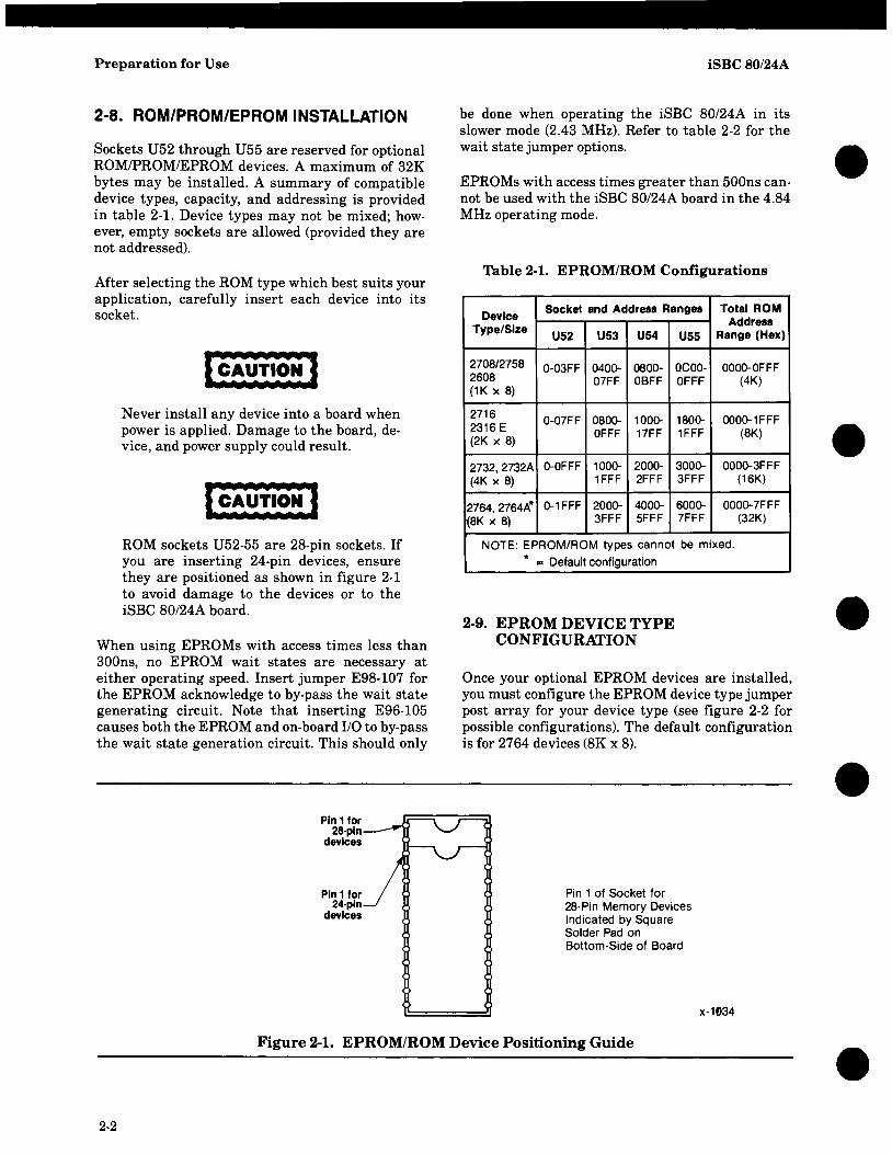
2-8. ROM/PROM/EPROM INSTALLATION
Sockets U52 through U55 are reserved for optional ROMIPROM/EPROM devices. A maximum of 32K bytes may be installed. A summary of compatible device types, capacity, and addressing is provided in table 2-1. Device types may not be mixed; however, empty sockets are allowed (provided they are not addressed).
After selecting the ROM type which best suits your application, carefully insert each device into its socket.
I~ Never install any device into a board when power is applied. Damage to the board, device, and power supply could result.
ROM sockets U52-55 are 28-pin sockets. If you are inserting 24-pin devices, ensure they are positioned as shown in figure 2-1 to avoid damage to the devices or to the iSBC 80/24A board.
When using EPROMs with access times less than 300ns, no EPROM wait states are necessary at either operating speed. Insert jumper E98-107 for the EPROM acknowledge to by-pass the wait state generating circuit. Note that inserting E96-105 causes both the EPROM and on-board I/O to by-pass the wait state generation circuit. This should only
Pin 1 for 28-pin
devices
Pin 1 for 24-pin
devices
iSBC 80/24A
be done when operating the iSBC 80/24A in its slower mode (2.43 MHz). Refer to table 2-2 for the wait state jumper options.
EPROMs with access times greater than 500ns cannot be used with the iSBC 80/24A board in the 4.84 MHz operating mode.
Table 2-1. EPROM/ROM Configurations
Device Socket and Address Ranges Total ROM
Type/Size Address
U52 U53 U54 U55 Range (Hex)
2708/2758 0-03FF 0400- 0800- OCOO- OOOo-OFFF 2608 (1 K x 8)
07FF OBFF OFFF (4K)
2716 0-07FF 0800- 1000- 1800- 0000-1FFF 2316 E OFFF 17FF 1FFF (8K) (2K x 8)
2732,2732A o-OFFF 1000- 2000- 3000- 0000-3FFF (4K x 8) 1FFF 2FFF 3FFF (16K)
2764, 2764A"" 0-1FFF 2000- 4000- 6000- 0000-7FFF (8K x 8) 3FFF 5FFF 7FFF (32K)
NOTE: EPROM/ROM types cannot be mixed.
"" = Default configuration
2-9. EPROM DEVICE TYPE CONFIGURATION
Once your optional EPROM devices are installed, you must configure the EPROM device type jumper post array for your device type (see figure 2-2 for possible configurations). The default configuration is for 2764 devices (8K x 8).
Pin 1 of Socket for 28-Pin Memory Devices Indicated by Square Solder Pad on Bottom-Side of Board
x-1fl34
Figure 2-1. EPROM/ROM Device Positioning Guide
2-2
•
•
•
•
•

•
•
•
•
•
iSBC80/24A Preparation for Use
Table 2-2. Wait State Jumpers
EPROM MAXIMUM ACCESS TIME (taee, In ns) 4.84 MHz Operating Speed 2.42 MHz Operating Speed
*
Wait State Jumpers Wait State Needed Needed Needed
tac > 300ns 0 E98-1 07 0
300 > tacc > 500 1* none 0
500 > tacc > 775 - - 0
= Default configuration
E177. • E178 E179 _ E180 E18l • • E182 El83 • • E184
2708 EPROM DEVICE E185 _ E186 (24-PIN) E187. • E188
E189_ • E19l E192_ • El94 E195_ • E197 El77 _ E178 El79 • • El80 E18l • • E182 E183. • E184
2758 EPROM DEVICE E185. • E186 (24-PIN) E187 _ E188
E189. _E19l E192_ • E194 E195_ • E197 E177 _ E178 E179. • E180 E18l • • E182 El83 _ El84
2716 EPROM DEVICE E185. • E186 (24-PIN) E187. • E188
E189. _E191 E192. _El94 E19S_ • E197
E177. • E178 E179. • E180 E181 _ E182 E183 _ E184
2732, 2732A EPROM DEVICES E18S. • E186 (24-PIN) E187. • E188
E189. _E19l E192 _
• E194 E195. _ E197
E177. • E178 E179. • El80 E18l _ E182 El83 _ E184
2764, 2764A EPROM DEVICES E185. • E18S (28-PIN) E187. • E188
DEFAULT CONFIGURATION E189. _E191 E192 • _El94 E195. .... E197
NOTE: SOLID BAR BETWEEN TWO JUMPER POSTS (E.G., El96-197) REPRESENTS A PUSH'()N JUMPER.
m-0393
Figure 2-2. EPROM Device Type Jumper Configuration
Jumpers Needed
E96-1 05 E96-1 05 E96-1 05
2-3

Preparation for Use
Incorrectly configuring the EPROM device type jumpers can result in damage to the EPROM devices and to the iSBC 80/24A board itself.
2-10. LINE DRIVERS AND 1/0 TERMINATORS
iSBC 80/24A
2-11. JUMPER CONFIGURATIONS
Either line driver and/or I/O terminator devices can be installed (as required) in sockets U2-U5 and U7-UI0. These sockets correspond to the 32 parallel I/O lines (without drivers or terminators). Ports E4 and E8 have Intel 8287 transceiver devices installed at the factory. Refer to table 2-3 for recommended I/O terminators and to table I-I (Chapter 1) for recommended line drivers for the iSBC 80/24A board.
Much of the flexibility of your iSBC 80/24A board is due to the use of jumper connections which may easily be altered from their default configurations to suit your particular application. Table 2-4 summarizes the jumper connections and their uses. Table 2-4A lists the jumper connections in numerical order, and indicates the factory default configurations. Physical locations of jumper posts on the board are shown in figure 5-3. Jumper connections are also shown schematically in figure 5·4.
NOTE Jumper posts are shown on the schematic diagrams with an E prefix (e.g., E86).
Table 2-3. Recommended 110 Terminators
I/O Terminator Pack
220/330 ohm Pull Up/Pull Down Terminator Pack
1 k ohm Pull Up Terminator Pack
Function
MUL TIBUS SIGNALS
AACKI
BPROI
8CLKI
CCLKI
BTMO
INTAI
PFSRI
TIMING & CPU
4.84 MHz Operation
2.42 MHz Operation
8224 OSC Output
RAM: AMOUNT ON-BOARD
2-4
Vendors/Part Number
iSBC 901
Beckman Instrument (Part #1899-746-1)
iSBC 902
Beckman Instrument (Part #1899-747-1)
Dale Electronics (Part #MOP14-00-593)
2-12. RAM CAPACITY AND ADDRESSING
The on-board RAM capacity and addressing is jumper configurable. The default configuration is 8K bytes of RAM from EOOO-FFFFH. To alter these configurations, refer to table 2-4 and section 4-10.
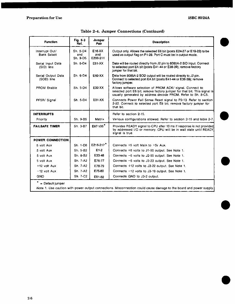
Table 2-4. Jumper Connections
Fig. 5-3 Jumper Description Ref. Pair
Sh. 2-06 E202-203 Connects AACKI signal from P1-25.
Sh. 2-03 E200-201 * Connects BPROI to P1-16.
Sh. 2-A6 E198-199 * Connects BCLKI to P1-13.
Sh. 2-A6 E204-205* Connects CCLKI to P1-31.
Sh. 3-A2 E220-221 * Connects BTMO to P2-34.
Sh. 3-82 E218-219* Connects INTAI to P2-36.
Sh. 5-04 E31-XX Connects 8224 OSC output to U20 Counter.
Sh. 3-05 E166-168* Uses 9.68 MHz clock input
Sh. 3-05 E163-166 Uses 4.84 MHz clock input
Sh. 3-C5 E96-105
Sh. 3-06 E171-174 * Connects 8224 OSC output to U20 Counter.
Sh. 4-C7 E109-100 Indicates 4K RAM on-board.
Sh. 4-C7 E1 09-1 00 Both jumpers in indicates 2K RAM; or E101-110 Both jumpers out indicates 8K RAM. (default configuration)
•
•
•
•
•

•
•
•
•
•
iSBC80/24A
Function
RAM ADDRESSING Selects maximum (hexadecimal)
8254 PIT
Inputs/Outputs
Gate Inputs
SERIAL PORT
Internal Clocks
RxC TxC
External Clocks
RxC TxC
Secondary RTS
Secondary TxO
Secondary CTS
Secondary RxO
Secondary TxC
Auxiliary Output 0 (AUXO/)
Auxiliary Input 1 (AUX1/)
Ring Indicator (input)
Received Line Signal Oetector (input)
PARALLEL PORTS
Operating Modes
* = Oefault jumper
Preparation for Use
Table 2-4. Jumper Connections (Continued)
Fig. 5-3 Ref.
Sh. 4-C5
Sh.7-C6
Sh. 5-04
Sh. 7-C6 Sh. 7-C6
Sh. 7-C6 Sh. 7-C6
Sh. 7-07
Sh. 7-07
Sh. 7-02
Sh. 7-02
Sh. 7-02
Sh. 6-04
Sh. 6-04
Sh. 6-04
Sh. 6-04
Sh. 5-04 Sh. 6-04
Jumper Pair
E112-113
E111-112
E1 03-1 04
Description
Note: To disable all on-board RAM, remove all jumpers from
2K 4K
3800-3FFF 3000-3FFF
7800-7FFF 700Q-7FFF
B800-BFFF BOOO-BFFF
8K
2000-3FFF
6000-7FFF
AOOQ-BFFF
posts E102, 103, 104,111,112 and 113.
E102-103* F80Q-FFFF FOOO-FFFF EOOO-FFFF ~------------~--------------------~------------~ NOTE: Install one jumper only.
E167-170 } Connects Timer 0 output to Timer 1 input.
E167-176 Connects Timer 0 output to Parallel port E6 jumper matrix.
E169-170* I E172-173*
E170-175 E173-175
E170-176 } E173-176
E172-176
E175-176
Provides 1.075 MHz to CLKO and CLK1 inputs.
Provides 134.4 KHz to CLKO and CLK1 inputs.
Connects parallel port E6 jumper matrix to one or more timer inputs.
Connects 1.075 MHz to parallel port E6 jumper matrix.
Connects 134.4 KHz to parallel port E6 jumper matrix. E13-28* I E14-29 * f Provides + 5 volts to gate 0 and gate 1 inputs of 8254 PIT.
E87-88* } E89-90*
E86-88 E89-91
E83-84
E84-85
E94-95
E93-95
E92-95
E47-XX
E62-XX
E46-XX
E45-XX
See table 2-7
Refer to section 2-13.
Connects PCI device to PIT Timer 2 output. (Baud rate clock)
Connects RxC input to J3-7. Connects TxC input to J3-3.
Connects J3-11 input to AUX1/ parallel port EA matrix.
Connects J3-1 input to AUX1/ parallel port EA matrix.
Connects J3-26 output to AUXO/ parallel port EA matrix.
Connects J3-5 output to AUXO/ parallel port EA matrix.
Connects J3-21 output to AUXO/ parallel port EA matrix.
Connects selected bit to jumper post E95. Connect to selected port EA bit; remove factory jumper for that bit. Use for Serial Channel protocol. See Sh. 7-02.
Connects J3-11 or J3-1 to selected EA bit via jumper matrix E83-84-85. See Sh. 7-07. Connect to selected port EA bit; remove factory jumper for that bit. Select one or both as required for Serial Channel protocol. Connects J3-17 input to selected port EA bit. Connect to selected port EA bit; remove factory jumper for that bit.
Connects J3-16 input to selected port EA bit. Connect to selected port EA bit; remove factory jumper for that bit.
Various configurations depending on 8255A mode and bit restrictions. Refer to section 2-14 and table 2-7.
2-5
Preparation for Use iSBC 80/24A
Table 2-4. Jumper Connections (Continued)
Function Fig. 5-3 Jumper
Description Ref. Pair • I nterru pt Outl Sh. 5-04 E16-XX Output only. Allows the selected E6 bit (posts E24-27 or E19-22) to be Bank Select and and used as output flag on P1·28. Port C must be in output mode.
Sh. 9-05 E206-211
Serial Input Data Sh.6-04 E61-XX Data will be routed directly from J2 pin to 8085A-2 SID input. Connect (SID) line to selected port EA bit (posts E41-44 or E36-39); remove factory
jumper for that bit.
Serial Output Data Sh. 6-04 E60-XX Data from 808SA-2 SOD output will be routed directly to J2 pin. (SOD) line Connect to selected port EA bit (posts E41-44 or E36·39); remove
factory jumper.
PROM Enable Sh. 5-04 E32-XX Allows software selection of PROM ACKI signal. Connect to selected port E6 bit; remove factory jumper for that bit. This signal is usually generated by address decode PROM. Refer to Sh. B-C5.
PFSRI Signal Sh. 5-04 E31-XX Connects Power Fail Sense Reset signal to P2-13. Refer to section 2-22. Connect to selected port E6 bit; remove factory jumper for that bit.
INTERRUPTS Refer to section 2-15.
Priority Sh. 9-B5 Matrix Various configurations allowed. Refer to section 2-15 and table 2-7. • FAILSAFE TIMER Sh. 3-B7 E97·106* Provides READY signal to CPU after 10 ms if response is not provided by addressed 1/0 or memory. CPU will be in wait state until READY signal is true.
POWER CONNECTION
5 volt Aux Sh. 1-06 E216-217* Connects +5 volt Main to +Sv Aux.
S volt Aux Sh. 5-B2 E1-2 Connects +5 volts to J1-S0 output. See Note 1.
5 volt Aux Sh. 6-B2 E33-4B Connects +S volts to J2-50 output. See Note 1.
S volt Aux Sh. 7-A2 E76-77 Connects +5 volts to J3-23 output. See Note 1.
+12 volt Aux Sh. 7-A2 E78-79 Connects +12 volts to J3-22 output. See Note 1. • -12 volt Aux Sh. 7-A2 E7S-80 Connects -12 volts to J3-19 output. See Note 1.
GND Sh. 7-C2 E81-82 Connects GNO to J3-2 output.
* = Default jumper
Note 1: Use caution with power output connections. Misconnection could cause damage to the board and power supply.
•
• 2-6

iSBC80/24A Preparation for Use
Table 2-4A. Numerical Listing of Jumpers
• Isac isac 80/24A 80/24A Sheet Function Text
Jumper Pair Grid Reference Ref.
1-2 5-B2 Connects +5 volts to J1-50 None 3-4* 5-C4 Configures port E4 bus transceiver to input mode 2-24
4-18 5-C4 Configures port E4 bus transceiver to output mode 2-14 5-19* 5-C4 Connects port E6, bit 0 to driver/terminator socket 2-14
6-20* 5-C4 Connects port E6, bit 1 to driver/terminator socket 2-14 7-21 * 5-C4 Connects port E6, bit 2 to driver/terminator socket 2-14 8-22* S-C4 Connects port E6, bit 3 to driver/terminator socket 2-14 9-24* 5-C4 Connects port E6, bit 4 to driver/terminator socket 2-14
10-25* 5-C4 Connects port E6, bit 5 to driver/terminator socket 2-14 11-26 * 5-C4 Connects port E6, bit 6 to driver/terminator socket 2-14 12-27* 5-C4 Connects port E6, bit 7 to driver/terminator socket 2-14 13-28* 5-C4 Applies + 5 volts to timer gate 0 (ITGO) None
• 14-29* 5-C4 Applies + 5 volts to ti mer gate 1 (ITG 1 ) None 15-30 5-C4 Connects timer 1 output to timer input matrix 2-11
1S-XX 5-C4 Connects selected J1 bit to timer input matrix 2-11
16-XX 5-C4 Connects INTROUT/BANKSEL to selected E6 bit 2-11 17-19 5-C4 Connects port E6, bit 0 to PIA 1 2-14 22-23 5-C4 Connects port E6, bit 3 to PIB1 2-14 31-XX 5-C4 Connects PFSR/ to selected E6 bit 2-22 32-XX 5-C4 Connects PROM ENABLE to selected E6 bit 2-11 33-48 6-B2 Connects + 5 volts to J2-SO None 34-35* 6-C4 Configures port E8 bus transceiver to input mode 2-14
• 35-50 6-C4 Configures port E8 bus transceiver to output mode 2-14 36-51 * 6-C4 Connects port EA, bit 0 to driver/terminator socket 2-14 37-52* 6-C4 Connects port EA, bit 1 to driver/terminator socket 2-14 38-53* 6-C4 Connects port EA, bit 2 to driver/terminator socket 2-14 39-54* 6-C4 Connects port EA, bit 3 to driver/terminator socket 2-14
40-XX 6-C4 Ground post 2-14 41-56* 6-C4 Connects port EA, bit 4 to driver/terminator socket 2-14 42-S7* 6-C4 Connects port EA, bit 5 to driver/terminator socket 2-14 43-58* 6-C4 Connects port EA, bit 6 to driver/terminator socket 2-14
• 44-S9* 6-C4 Connects port EA, bit 7 to driver/terminator socket 2-14 45-XX 6-C4 Connects BDET/ to selected EA bit 2-14 46-XX 6-C4 Connects BRI/ to selected EA bit 2-14 47-XX 6-C4 Connects AUXO/ to selected EA bit 2-14 49-S1 6-C4 Connects port EA, bit 0 to PIA2/ 2-14 54-55 6-C4 Connects port EA, bit 3 to PIA 1/ 2-14 60-XX 6-C4 Connects SOD to selected EA bit 2-14 61-XX 6-C4 Connects SID to selected EA bit 2-14 62-XX 6-C4 Connects AUX1/ to selected EA bit 2-14 63-64 * 7-C3 Connects transmit data to J3-4 2-13 63-74 7-C3 J3 serial jumper matrix 2-13 65-66* 7-C3 Connects receive data to J3-6 2-13 67-68* 7-C3 Connects RTS to J3-8 2-13 69-70* 7-C3 Con nects CTS to J3-1 0 2-13 71-72* 7-C3 Connects DSR to J3-12 2-13 73-74 * 7-C3 Connect DTR to J3-13 2-13 7S-80 7-A2 • Connects -12 volts to J3-19 2-25
2-7
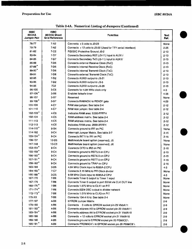
Preparation for Use iSBC 80/24A
Table 2-4A. Numerical Listing of Jumpers (Continued)
iSBC iSBC 80/24A 80/24A Sheet Function Text
Jumper Pair Grid Reference Ref. • 76-77 7-A2 Connects + 5 volts to J3-23 None 78-79 7-A2 Connects + 12 volts to J3-22 (Used for TTY serial interface) 2-25 81-82 7-C2 RS232C Protective Ground J3-2 2-13 83-84 7-07 Connects Secondary RST (J3-11) input to AUX1f 2-13 84-85 7-07 Connects Secondary TxO (J3-11) input to AUX11 2-13 86-88 7-06 Connects external Receive Clock (RxC) 2-13 87-88* 7-06 Connects internal Receive Clock (RxC) 2-13 89-90* 7-06 Connects internal Transmit Clock (TxC) 2-13 89-91 7-06 Connects external Transmit Clock (TxC) 2-13 92-95 7-02 Connects AUXOI output to J3-21 2-13 93-95 7-02 Connects AUXOI output to J3-5 2-13 94-95 702 Connects AUXOI output to J3-26 2-13 96-105 3-C5 Connects for 4.84 MHz clock only 4-3 97-106 * 3-86 Enables failsafe timer 4-35
98-107 3-87 Reserved None • 99-108 * 3-87 Connects RAMACKI to READY gate 4-29 100-109 4-C7 RAM size jumper. See table 2-4 2-12 101-110 4-C7 RAM size jumper. See table 2-4 2-12
102-103* 4-C5 Indicates RAM area: EOOO-FFFFH 2-12 102-104 4-C5 RAM address matrix. See table 2-4 2-12 111-113 4-C5 RAM address matrix. See table 2-4 2-12 112-113 4-C5 Indicates RAM area: 2000-3FFFH 2-12 114-115* 9-84 Connects ground to IR7 on PIC None 114-162 9-C4 Interrrupt Jumper Matrix. See table 2-7 2-15 133-134 * 9-C4 Connects INT11 to IR1 on PIC 2-15 • 136-137 10-05 Multimodule board option (reserved); J5 None 147-148 10-C3 Multimodule board option (reserved); J6 None 153-154* 9-C4 Connects OITO to IR2 on PIC 2-15 155-159* 9-C4 Connects ground to RST5.5 on CPU 2-15 156-160 * 9-C4 Connects ground to RST6.5 on CPU 2-15 157-161* 9-C4 Connects ground to RST7.5 on CPU 2-15 158-162* 9-C4 Connects ground to TRAP on CPU 2-15 163-166 3-05 4.84 MHz Clock input to 8085A-2 CPU 4-3 164-165* 7-C7 Connects 2.15 M Hz to PIT Clock divider None • 166-168 * 3-05 9.68 MHz Clock input to 8085A-2 CPU 4-3 167-170 7-86 Connects Timer 0 output to Timer 1 input None 167-176 7-86 Connects Timer 0 output to port E6 bit via ClK OUT line None 169-170* 7-86 Connects 1.075 MHz to ClK1 on PIT None 171-174* 7-86 Connects 8224 OSC output to divider network None 172-173 * 7-86 Connects 1.075 MHz to ClKO on PIT None 175-XX 7-86 Connects 134.4 KHz: See table 2-4 None 177-197 4-86 EPROM Jumper Matrix 2-9 179-180 4-86 Connects -5 volts to EPROM socket pin 23 Vbb/A11 2-9 181-182* 4-86 Connects address AB to EPROM socket pin 23 Vbb/A 11 2-9 183-184 * 4-86 Connects address AA to EPROM socket pin 21 Vdd/A10 2-9 185-186 4-86 Connects + 12 volts to EPROM socket pin 21 Vdd/A 10 2-9 189-190 4-86 Connects ground to EPROM socket pin 20 PGM/CE\ 2-9 190-191 * 4-86 Connects PROMACK\ to EPROM socket pin 20 PGM/CE\ 2-9 •
2-8
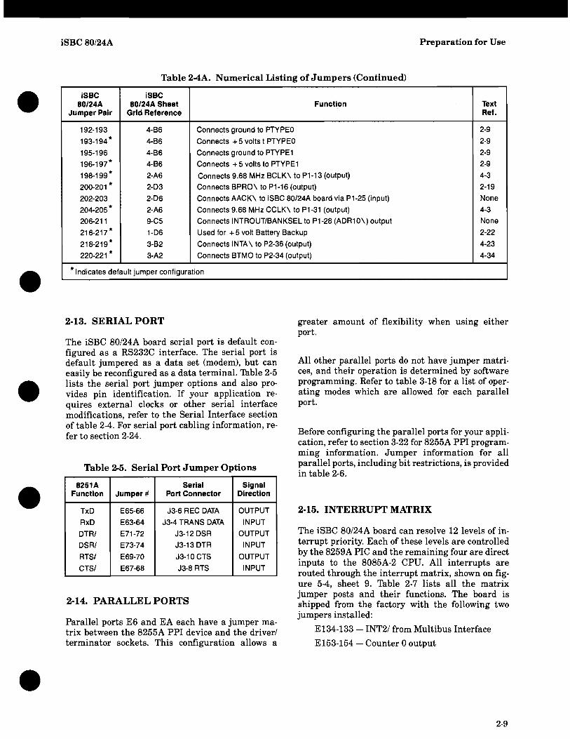
•
•
•
•
•
iSBC80/24A Preparation for Use
Table 2-4A. Numerical Listing of Jumpers (Continued)
isac Isac 80/24A 80/24A Sheet Function Text
Jumper Pair Grid Reference Ref.
192-193 4-86 Connects ground to PTYPEO 2-9
193-194 * 4-86 Connects + 5 volts t PTYPEO 2-9
195-196 4-86 Connects ground to PTYPE1 2-9
196-197* 4-86 Connects + 5 volts to PTYPE1 2-9
198-199* 2-A6 Connects 9.68 MHz BCLK\ to P1-13 (output) 4-3.
200-201 * 2-03 Connects BPRO\ to P1-16 (output) 2-19
202-203 2-06 Connects AACK\ to iSBC 80/24A board via P1-25 (input) None
204-205* 2-A6 Connects 9.68 MHz CCLK\ to P1-31 (output) 4-3
206-211 9-C5 Connects INTROUT/BANKSEL to P1-28 (ADR10\) output None
216-217* 1-06 Used for + 5 volt Battery Backup 2-22
218-219 * 3-B2 Connects INTA \ to P2-36 (output) 4-23
220-221 * 3-A2 Connects BTMO to P2-34 (output) 4-34
* Indicates default jumper configuration
2-13. SERIAL PORT
The iSBC 80/24A board serial port is default con· figured as a RS232C interface. The serial port is default jumpered as a data set (modem), but can easily be reconfigured as a data terminal. Table 2-5 lists the serial port jumper options and also pro· vides pin identification. If your application reo quires external clocks or other serial interface modifications, refer to the Serial Interface section of table 2-4. For serial port cabling information, reo fer to section 2-24.
Table 2-5. Serial Port Jumper Options
8251A Serial Signal Function Jumper # Port Connector Direction
TxD E65-66 J3-6 REC DATA OUTPUT
RxD E63-64 J3-4 TRANS DATA INPUT
DTRI E71-72 J3-12DSR OUTPUT
DSRI E73-74 J3-13DTR INPUT
RTSI E69-70 J3-10 CTS OUTPUT
CTSI E67-68 J3-8 RTS INPUT
2-14. PARALLEL PORTS
Parallel ports E6 and EA each have a jumper mao trix between the 8255A PPI device and the driver/ terminator sockets. This configuration allows a
greater amount of flexibility when using either port.
All other parallel ports do not have jumper matri· ces, and their operation is determined by software programming. Refer to table 3-18 for a list of opere ating modes which are allowed for each parallel port.
Before configuring the parallel ports for your appli. cation, refer to section 3-22 for 8255A PPI program· ming information. Jumper information for all parallel ports, including bit restrictions, is provided in table 2-6.
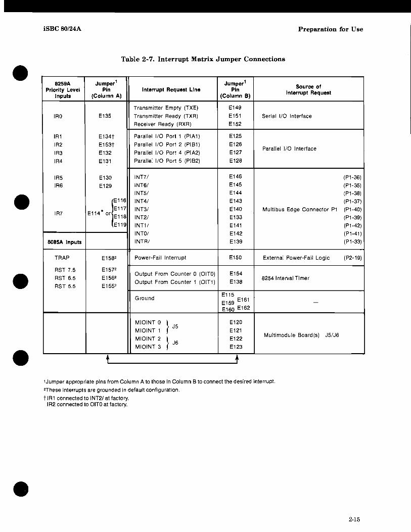
2-15. INTERRUPT MATRIX
The iSBC 80/24A board can resolve 12 levels of in· terrupt priority. Each of these levels are controlled by the 8259A PIC and the remaining four are direct inputs to the 8085A-2 CPU. All interrupts are routed through the interrupt matrix, shown on fig· ure 5-4, sheet 9. Table 2-7 lists all the matrix jumper posts and their functions. The board is shipped from the factory with the following two jumpers installed:
E134-133 - INT2/ from Multibus Interface
E153-154 - Counter 0 output
2-9

Preparation for Use iSBC 80/24A
Table 2-6. Configuration Jumpers for Parallel Ports E4 - EA
Jumper Configuration Driver (0)1 • Port Mode Terminator (T) Remove Add Effect Port Restrictions
E4 ° 8287:U1 E3-4 * E4-18 8287 = input enabled. ES None; can be in Mode ° or 1, Input input or output.
E6 None; can be in Mode 0, input or output, unless Port ES is in Mode 1.
E4 ° 8287:U1 None E3-4* 8287 = output enabled. ES None; can be in Mode ° or 1, Output input or output.
(latched) E6 None; can be in Mode 0, input
or output, unless Port ES is in Mode 1.
E4 1 8287:U1 E3-4* E4-18 8287 = output enabled. ES None; can be in Mode ° or 1, . Input T: U2 input or output.
(strobed) - E9-24 * Connects J1-26 to E6 Port E6 bits perform the fol-D:U3 STBAI input. owing:
E1 0-25 * E8-25 Connects IBFA output • Bits 0, 1, 2 - Control for • and to J1-18. Port ES if in Mode 1.
E8-22* - Disconnect Port E6, • Bit 3 - Port E4 Interrupt to bit 3 (INTR) from driver interrupt jumper matrix. at U3.
• Bit 4 - Port E4 Strobe (STB/) input.
• Bit 5 - Port E4 Input Buffer Full (I BF) output.
• Bits 6, 7 - Port E6 input or output (both must be in same direction).
E4 1 8287:U1 - E3-4 * 8287 = output enabled. E5 None; can be in Mode ° or 1, • Output T: U2 input or output. (latched) - E11-26 * Connects J1-30 to E6 Port E6 bits perform the fol-D:U3
ACKA/ input. lowing:
E12-27* E8-27 Connects OBFAI out- • Bits 0, 1, 2 - Control for and put to J1-18. Port ES if in Mode 1.
E8-22* - Disconnect Port E6, • Bit 3 - Port E4 Interrupt to bit 3 (INTR) from driver interrupt jumper matrix. at U3.
• Bits 4, S - Input or output (both must be in same direction). • • Bit 6 - Port E4 Acknow-ledge (ACK/) input.
• Bit 7 - Port E4 Output Buffer Full (OBF/) output.
E4 2 8287:U1 E3-4* E4-26 Allows ACKAI output E5 None. (bidirectional) T: U3 to control 8287 inlout
E6 Port E6 bits perform the fol-direction. lowing:
- E9-24* Connects J1-26 to STBA input. • Bit ° - Cannot be used.
E10-2S * E5-25 Connects IBFA output • Bits 1, 2 - Can be used for and to J1-24. input or output if Port E5 is
E5-19 * in Mode O.
- E11-26* Connects J1-30 to • Bit 3 - Port E4 Interrupt
ACKAI input. to interrupt jumper matrix.
E12-27* E8-27 Cor.mects OBFAI out- • Bit 4 - Port E4 Strobe
put to J1-18. (STB/) input.
* Default jumper connected at the factory. • 2-10
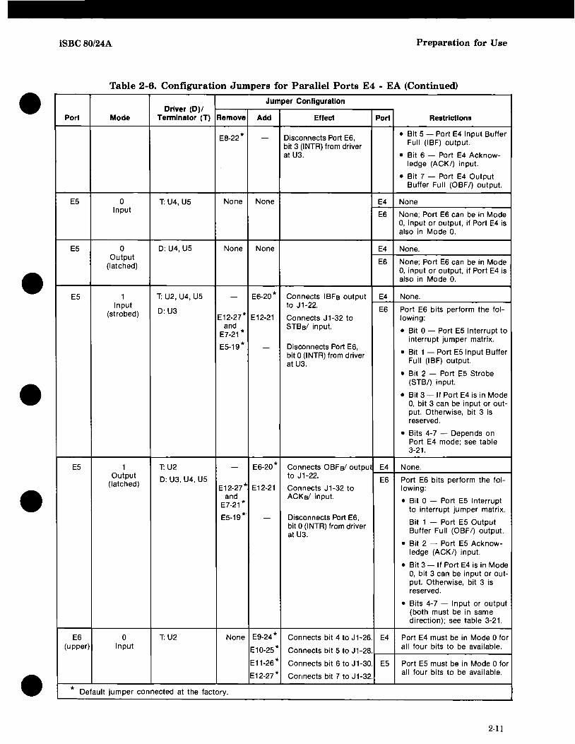
iSBC 80/24A Preparation for Use
Table 2-6. Configuration Jumpers for Parallel Ports E4 - EA (Continued)
• Jumper Configuration Driver (0)/
Port Mode Terminator (T) Remove Add Effect Port Restrictions
ES-22 * - Disconnects Port ES, • Bit 5 - Port E4 Input Buffer
bit 3 (INTR) from driver FIJII (IBF) output.
at U3. • Bit S - Port E4 Acknow-ledge (ACK/) input.
• Bit 7 - Port E4 Output Buffer Full (OBF/) output.
E5 ° T: U4, US None None E4 None Input
ES None; Port ES can be in Mode 0, input or output, if Port E4 is also in Mode O.
E5 0 D:U4,US None None E4 None.
• Output
E6 None; Port ES can be in Mode (latched) 0, input or output, if Port E4 is also in Mode O.
E5 1 T: U2, U4, US - E6-20 * Connects IBFa output E4 None. Input to J1-22. E6 Port E6 bits perform the fol-(strobed) D:U3
E12-27* E12-21 Connects J1-32 to lowing: and STBeI input.
• Bit 0 - Port E5 Interrupt to E7-21 *
ES-19* interrupt jumper matrix.
- Disconnects Port E6, • Bit 1 - Port ES Input Buffer bit 0 (INTR) from driver
at U3. Full (IBF) output.
• Bit 2 - Port ES Strobe
• (STB/) input.
• Bit 3 - If Port E4 is in Mode 0, bit 3 can be input or out-put. Otherwise, bit 3 is reserved.
• Bits 4-7 - Depends on Port E4 mode; see table 3-21.
ES 1 T: U2 - E6-20 * Connects OBFeI output E4 None.
• Output D:U3,U4,US to J1-22. E6 Port E6 bits perform the fol-(latched) E12-27 * E12-21 Connects J1-32 to lowing:
and ACKeI input. • Bit 0 - Port E5 Interrupt E7-21 *
to interrupt jumper matrix. ES-19*' - Disconnects Port E6,
Bit 1 - Port ES Output bit 0 (INTR) from driver at U3. Buffer Full (OBF/) output.
• Bit 2 - Port ES Acknow-ledge (ACK/) input.
• Bit 3 - If Port E4 is in Mode 0, bit 3 can be input or out-put. Otherwise, bit 3 is reserved.
• Bits 4-7 - Input or output (both must be in same direction); see table 3-21.
ES ° T: U2 None E9-24*' Connects bit 4 to J1-2S. E4 Port E4 must be in Mode 0 for (upper) Input E1 0-2S * Connects bit S to J1-2S. all four bits to be available.
E11-2S* Connects bit S to J1-30. E5 Port E5 must be in Mode 0 for
• E12-27* Connects bit 7 to J1-32. all four bits to be available.
* Default jumper connected at the factory.
2-11

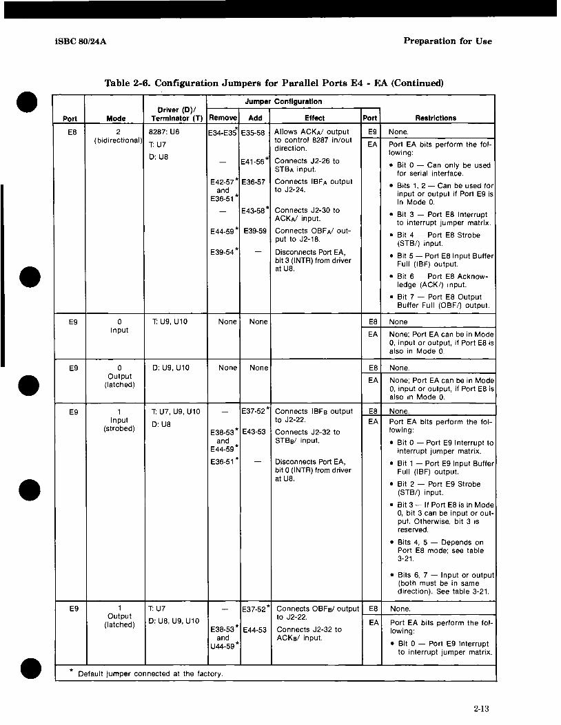
Preparation for Use iSBC 80/24A
Table 2-6. Configuration Jumpers for Parallel Ports E4 - EA (Continued)
Jumper Configuration Driver (0)/ • Port Mode Terminator (T) Remove Add Effect Port Restrictions
E6 0 T: U3 None ES-19* Connects bit 0 to J1-24. E4 Port E4 must be in Mode 0 for (lower) Input E6-20* Connects bit 1 to J1-22. all four bits to be available.
E7-21 * Connects bit 2 to J1-20. E5 Port E5 must be in Mode 0 for
E8-22 * Connects bit 3 to J1-18. all four bits to be available.
E6 0 D:U2 None Same as for Port E6 (upper) E4 Same as for Port E6 (upper) (upper) Output Mode 0 Input. & Mode 0 Input.
(latched) E5
E6 0 D:U3 None Same as for Port E6 (lower) E4 Same as for Port E6 (lower) (lower) Output Mode 0 Input. & Mode 0 Input.
(latched) ES
E8 0 8287: U6 E34-3S* E3S-S0 8287 = input enabled. E9 None; can be in Mode 0 or 1, Input input or output.
EA None; can be in Mode 0, input or output, unless Port E9 is • in Mode 1.
E8 0 8287: U6 None E34-3S* 8287 = output enabled. E9 None; can be in Mode 0 or 1, Output input or output.
(latched) EA None; can be in Mode 0, input
or output, unless Port E9 is in Mode 1.
E8 1 8287: U6 E34-3S* E3S-S0 8287 = output enabled. E9 None; can be in Mode 0 or 1, Input T: U7 input or output.
(strobed) - E41-S6* Connects J2-26 to EA Port EA bits perform the fol-D:U8 STBAI input. owing: • E42-S7* E39-S7 Connects IBFA output • Bits 0, 1, 2 -- Control for to J2-18. Port E9 if in Mode 1.
E39-S4 * - Disconnects Port EA. • Bit 3 - Port E8 Interrupt to bit 3 (INTR) from driver interrupt jumper matrix. at U8.
• Bit 4 - Port E8 Strobe (STB/) input.
• Bit 5 - Port E8 Input Buffer Full (IBF) output.
• Bits 6. 7 - Port EA input or output (both must be in same direction). •
E8 1 8287: U6 - E34-3S* 8287 = output enabled. E9 None; can be in Mode 0 or 1, Output T: U7 input or output.
(latched) - E43-S8* Connects J2-30 to EA Port EA bits perform the fol-D:U8 ACKAI input. lowing:
E44-S9* E39-S9 Connects OBFAI out- • Bits 0, 1, 2 - Control for put to J2-18. Port E9 if in Mode 1.
E39-S4 * - Disconnects Port EA, • Bit 3 - Port E8 Interrupt to bit 3 (INTR) from driver interrupt jumper matrix. at U8.
• Bits 4, 5 - Input or output (both must be in same direction) .
• Bit 6 - Port E8 Acknow-ledge (ACK/) input.
• Bit 7 - Port E8 Output Buffer Full (OBF/) output.
* Default jumper connected at the factory. • 2-12
iSBC 80/24A Preparation for Use
Table 2-6. Configuration Jumpers for Parallel Ports E4 - EA (Continued)
• Jumper Configuration Driver (0)/
Port Mode Terminator (T) Remove Add Effect Port Restrictions
E8 2 8287:U6 * Allows ACKAI output E9 None. E34-E35 E35-5S (bidirectional) T: U7
to control 8287 in/out EA Port EA bits perform the fol-direction.
D:US lowing:
- E41-56* Connects J2-26 to • Bit 0 - Can only be used STBA input. for serial interface.
E42-57* E36-57 Connects IBFA output • Bits 1,2 - Can be used for
and to J2-24. E36-51 *
input or output if Port E9 is in Mode O.
• - E43-5S* Connects J2-30 to
• Bit 3 - Port E8 Interrupt ACKAI input. to interrupt jumper matrix. E44-59* E39-59 Connects OBFAI out-
• Bit 4 - Port ES Strobe put to J2-18. (STB/) input.
E3S-54 * - Disconnects Port EA, • Bit 5 - Port E8 Input Buffer bit 3 (INTR) from driver Full (IBF) output. at US.
• Bit 6 - Port E8 Acknow-ledge (ACK/) input.
• Bit 7 - Port ES Output Buffer Full (OBF/) output.
ES 0 T:U9,U10 None None E8 None Input EA None; Port EA can be in Mode
0, input or output, if Port EB is also in Mode O.
E9 0 D:U9,U10 None None E8 None.
• Output EA None; Port EA can be in Mode (latched) 0, input or output, if Port EB is also in Mode O.
E9 1 T: U7, U9, U10 - E37-52* Connects IBFs output EB None. Input
D:US to J2-22. EA Port EA bits perform the fol-
(strobed) E3B-53* E43-53 Connects J2-32 to lowing:
and STBsl input. • Bit 0 - Port ES Interrupt to E44-5S* interrupt jumper matrix.
• E36-S1 * - Disconnects Port EA, • Bit 1 - Port E9 Input Buffer
bit 0 (INTR) from driver Full (IBF) output. at UB.
• Bit 2 - Port ES Strobe (STB/) input.
• Bit 3 - If Port EB is in Mode 0, bit 3 can be input or out-put. Otherwise, bit 3 is reserved.
• Bits 4, 5 - Depends on Port EB mode; see table 3-21.
• Bits 6, 7 - Input or output (both must be in same direction). See table 3-21.
E9 1 T: U7 - E37-52* Connects OBFsl output EB None. Output
D:US,U9,U10 to J2-22. (latched) EA Port EA bits perform the fol-
E3S-53* E44-53 Connects J2-32 to lowing: and ACKsl input.
U44-5S* • Bit 0 - Port E9 Interrupt to interrupt jumper matrix .
• * Default jumper connected at the factory.
2-13

Preparation for iSBC 80/24A
Table 2-6. Configuration Jumpers for Parallel Ports E4 - EA (Continued)
Jumper Configuration
Driver (0)/ Port Mode Terminator (n Remove Add Effect Port Restrictions
E36-51 * - Disconnects Port EA. Bit 1 - Port E9 Output bit 0 (INTR) from driver Buffer Full (OBF/) output. at U8.
• Bit 2 - Port E9 Acknow-ledge (ACK/) input.
• Bit 3 - If Port E8 is in Mode O. bit 3 can be input or out-put. Otherwise. bit 3 is reserved .
• Bits 4-7 - Input or output (both must be in same direction): see table 3-21.
EA 0 T: U7 None E41-56* Connects bit 4 to J2-26. E8 Port E8 must be in Mode 0 for (upper) Input
E42-57* Connects bit 5 to J2-28. all four bits to be available.
E43-58* Connects bit 6 to J2-30. E9 Port E9 must be in Mode 0 for
E44-59* Connects bit 7 to J2-32. all four bits to be available.
EA 0 T: U8 None E36-51 * Connects bit 0 to J2-24. E8 Port E8 must be in Mode 0 for (lower) Input E37-52* Connects bit 1 to J2-22. all four bits to be available.
E38-53* Connects bit 2 to J2-20. E9 Port E9 must be in Mode 0 for
E39-54* Connects bit 3 to J2-18. all four bits to be available.
EA 0 D:U7 None Same as for Port EA (upper) E8 Same as for Port EA (upper) (upper) Output Mode 0 Input. & Mode 0 Input.
(latched) E9
EA 0 D:U8 None Same as for Port EA (lower) E8 Same as for Port EA (lower) (lower) Output Mode 0 Input. & Mode 0 Input.
(latched)
* Default jumper connected at the factory.
Refer to section 3-30 for 8259A PIC programming information, and section 3-37 for 8085A-2 CPU interrupt handling.
2·16. CONNECTOR INFORMATION
For systems applications, the iSBC SO/24A board is designed for installation into a standard Intel iSBC 604/614 Cardcage assembly. For OEM applications the board may be interfaced to other hardware by means of separately purchased connectors. Table 2-S lists recommended suppliers for each iSBC SO/24A board connector.
2·17. MULTIBUS® SIGNAL CHARACTERISTICS
Connectors PI and P2 interface your iSBC 80/24A board signals and power lines to the power supply and other boards in your system. Where applicable,
2-14
E9
these signals conform to the Intel Multibus Interface standard. Pin assignments for PI and P2 are listed in tables 2-9 and 2-11 respectively. Brief descriptions of these signals are provided in tables 2-10 and 2-12.
AC characteristics, with the board operating at 4.S4 MHz are provided in table 2-13. With the board operating at 2.42 MHz, these parameters are shown in table 2-14. A system timing diagram is provided in figure 2-3.
DC characteristics for PI signals are provided in table 2-15; P2 signal characteristics are shown in table 2-16.
2-18. PARALLEL 110 DC CHARACTERISTICS
Parallel I/O DC characteristics for connectors Jl and J2 are provided in table 2-17.
•
•
•
•
•
•
•
•
•
•
iSBC80/24A Preparation for Use
Table 2-7. Interrupt Matrix Jumper Connections
8259A Jumper1 Jumper1 Source of
Priority Level Pin Interrupt Request Line Pin Interrupt Request Inputs (Column A) (Column B)
Transmitter Empty (TXE) E149
IRO E135 Transmitter Ready (TXR) E151 Serial I/O Interface
Receiver Ready (RXR) E152
IR1 E134t Parallel I/O Port 1 (PIA1) E125
IR2 E153t Parallel I/O Port 2 (PIB1) E126 Parallel I/O Interface
IR3 E132 Parallel I/O Port 4 (PIA2) E127
IR4 E131 Parallel I/O Port 5 (PIB2) E128
IR5 E130 INT7/ E146
IR6 E129 INT6/ E145
INT5/ E144
r"o INT4/ E143
* E117 INT3/ E140 Multlbus Edge Connector P1 IR7 E114 or E118 INT2/ E133
E119 INT1/ E141
INTO/ E142
8085A Inputs INTR/ E139
TRAP E1582 Power-Fail Interrupt E150 External Power-Fail Logic
RST 7.5 E1572 Output From Counter 0 (OITO) E154
RST 6.5 E1562 8254 Interval Timer Output From Counter 1 (0IT1) E138
RST 5.5 E1552
Ground E115 E159 E161 -E160 E162
MIOINT 0 } J5
E120
MIOINT 1 E121
MIOINT 2 } J6
E122 Multimodule Board(s) J5/J6
MIOINT 3 E123
+ .. 'Jumper appropriate pins from Column A to those in Column B to connect the desired interrupt.
2These interrupts are grounded in default configuration.
t IR1 connected to INT21 at factory. IR2 connected to OITO at factory.
(P1-36)
(P1-35) (P1-38)
(P1-37)
(P1-40)
(P1-39)
(P1-42) (P1-41)
(P1-33)
(P2-19)
2-15
Preparation for Use iSBC 80f24A
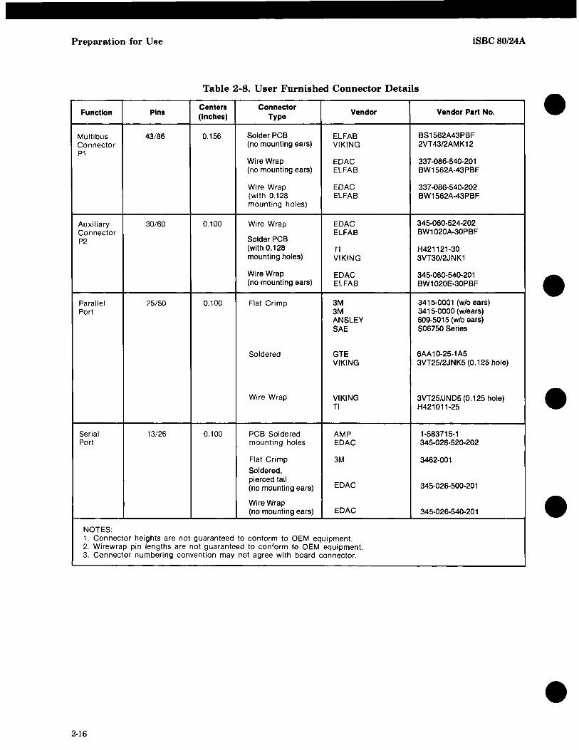
Table 2-8. User Furnished Connector Details
Function Pins Centers Connector
Vendor Vendor Part No. (Inches) Type •
Multibus 43/86 0.156 Solder PCB ELFAB BS1562A43PBF Connector (no mounting ears) VIKING 2VT43/2AMK12 P1
Wire Wrap EDAC 337-086-540-201 (no mounting ears) ELFAB BW1562A-43PBF
Wire Wrap EDAC 337-086-540-202 (with 0.128 ELFAB BW1562A-43PBF mounting holes)
Auxiliary 30/60 0.100 Wire Wrap EDAC 345-060-524-202 Connector ELFAB BW1020A-30PBF P2 Solder PCB
(with 0.128 TI H421121-30 mounting holes) VIKING 3VT30/2JNK1
Wire Wrap EDAC 345-060-540-201 (no mounting ears) ELFAB BW1020E-30PBF • Parallel 25/50 0.100 Flat Crimp 3M 3415-0001 (w/o ears)
Port 3M 3415-0000 (w/ears) ANSLEY 609-5015 (w/o ears) SAE S06750 Series
Soldered GTE 6AA 10-25-1 A5 VIKING 3VT25/2JNK5 (0.125 hole)
Wire Wrap VIKING 3VT25/JND5 (0.125 hole) TI H421011-25 •
Serial 13/26 0.100 PCB Soldered AMP 1-583715-1 Port mounting holes EDAC 345-026-520-202
Flat Crimp 3M 3462-001 Soldered, pierced tail
EDAC 345-026-500-201 (no mounting ears)
Wire Wrap (no mounting ears) EDAC 345-026-540-201 • NOTES:
1. Connector heights are not guaranteed to conform to OEM equipment. 2. Wirewrap pin lengths are not guaranteed to conform to OEM equipment. 3. Connector numbering convention may not agree with board connector.
• 2-16

iSBC80/24A Preparation for Use
• Table 2-9. Connector PI Pin Assignments
(Component Side) (Circuit Side) Pin Pin
Mnemonic Description Mnemonic Description
1 GND Signal GND 2 GND Signal GND
3 +5V +5Vdc 4 +5V +5Vdc
POWER 5 +5V +5Vdc 6 +5V +5Vdc
SUPPLIES 7 +12V +12Vdc 8 +12V +12Vdc
9 -5V -5Vdc 10 -5V -5Vdc
11 GND Signal GND 12 GND Signal GND
13 BCLKI Bus Clock 14 INITI Initialize
15 BPRNI Bus Priority In 16 BPROI Bus Priority Out
BUS 17 BUSYI Bus Busy 18 BREQI Bus Request
CONTROLS 19 MRDCI Mem Read Cmd 20 MWTCI Mem Write Cmd
21 10RCI 1/0 Read Cmd 22 10WCI 1/0 Write Cmd
• 23 XACKI XFER Acknowledge 24 Reserved
25 Reserved 26 Reserved BUS
27 Reserved 28 ADR101 Address 10 CONTROLS
29 CBRQI Common Bus Request 30 Reserved AND
31 CCLKI Constant Clock 32 Reserved ADDRESS
33 Reserved 34 Reserved
35 INT61 36 INT71
37 INT41 Interrupt 38 INT51 Interrupt INTERRUPTS
39 INT21 Requests 40 INT31 Requests
• 41 INTOI 42 INT11
43 ADREI 44 ADRFI 45 ADRCI 46 ADRDI 47 ADRAI Address 48 ADRBI Address 49 ADR81 Bus 50 ADR91 Bus
ADDRESS ADR61 51 52 ADR7/
53 ADR41 54 ADR5/
55 ADR21 56 ADR3/
57 ADRO/ 58 ADR1/
• 59 Reserved 60 Reserved
61 Reserved 62 Reserved
63 Reserved 64 Reserved
65 Reserved 66 Reserved DATA
67 DAT6/ Data Bus 68 DAT7I Data Bus
69 DAT4/ Data Bus 70 DAT5/ Data Bus 71 DAT2/ Data Bus 72 DAT3/ Data Bus
73 DATO/ Data Bus 74 DAT1/ Data Bus
75 GND Signal GND 76 GND Signal GND 77 Reserved 78 Reserved
POWER 79 -12V -12Vdc 80 -12V -12Vdc
SUPPLIES 81 +5V +5Vdc 82 +5V +5Vdc 83 +5V -5Vdc 84 +5V +5Vdc 85 GND Signal GND 86 GND Signal GND
• NOTE: All odd-numbered pins (1,3,5 ... 85) are on component side of the board. Pin 1 is the left-most pin when viewed from the component side of the board with the extractors at the top. All unassigned pins are reserved.
2-17

Preparation for Use
BCLKI
INITI
BPRNI
BPROI
BREQI
MRDCI
MWTCI
10RCI
10WCI
XACKI
CCLKI
INTOI - INT71
ADROI - ADRFI
DATOI - DAT7I
CBRQI
2-18
iSBC 80/24A
Table 2-10. Connector PI Signal Definitions
Bus clock; used to synchronize bus control circuits on all master modules. BCLKI has a period of 103.3 nanoseconds (9.677 MHz frequency), 50% duty cycle. BCLKI may be slowed, stopped or single stepped if desired.
Initialization signal; resets the entire system to a known internal state.
Bus priority input signal; indicates to the iSBC 80!24A board that no higher priority master module is requesting use of the system bus. BPRNI must be synchronized with BCLKI in multi-master system; BPRN! must be connected to signal ground in a single-master system.
Bus priority out signal; used with serial (daisy chain) bus priority resolution schemes. BPROI is passed to the BPRNI input of the master module with next lower bus priority.
Bus request signal; used with a parallel bus priority network to indicate that a particular master module requires use of the bus for one or more data transfers. BREQI is synchronized with BCLK/.
Memory read command; indicates that the address of a memory location has been placed on the system address lines and specifies that the contents of the addressed location are to be read and placed on the system data bus.
Memory write command; indicates that the address of a memory location has been placed on the system address lines and that a data word has been placed on the system data bus. MWTCI specifies that the data word is to be written into the addressed memory location.
I/O read command; indicates that the address of an input port has been placed on the system address bus and that the data at that input port is to be read and placed on the system data bus.
liD write command; indicates that the address of an output port has been placed on the system address bus and that the contents of the system data bus are to be output to the addressed port.
Transfer acknowledge signal; the required response of an external memory location or 1/0 port which indicates that the specified readlwrite operation has been completed. That is, data has been placed on, or accepted from the system data bus lines.
Constant clock; provides a clock signal of constant frequency (9.677 MHz) for use by optional memory and 1/0 expansion boards. CCLKI has a period of 103.3 nanoseconds, 50% duty cycle.
Externally generated interrupt requests.
16 Address lines; used to transmit the address of the memory location or 1/0 port to be accessed. ADRFI is the most significant bit.
Bi-directional data lines; used to transmit/receive information tolfrom a memory location or 110 port. DA T7 I is the most significant bit.
Common Bus Request; indicates that a bus master wishes control of the bus but does not presently have control. As soon as control of the bus is obtained, the requesting bus controller raises the CBRQI signal.
•
•
•
•
•

•
•
•
•
•
iSBC 80/24A
PFINI
PFSNI
PFSR/
MPROI
HALT/
ALE
Preparation for Use
Table 2-11. Connector P2 Pin Assignments
Pin Signal Description Assignment Mnemonic
P2-1, 2 Signal GND Battery Ground P2-21, 22
P2-3 +5V AUX Battery +5V Power Input P2-4
P2-13 PFSRI Power Fail Sense Reset
P2-17 PFSNI Power Fail Sense
P2-19 PFINI Power Fail Interrupt
P2-20 MPROI Memory Protect
P2-28 HALT/ Halt Indicator
P2-32 ALE Bus Master ALE
P2-34 BTMO Bus Timeout
P2-36 INTAI Interrupt Acknowledge
P2-38 AUX RESETI System Reset Switch Input
Table 2-12. Connector P2 Signal Definitions
Power Fail Interrupt. This input from the power supply interrupts the CPU when a power failure occurs. See section 2-22.
Power Fail Sense. This line is the output of a latch which indicates a power failure has occurred. It is reset by PFSR/ and must be powered by the standby power source. See section 2-22.
Power Fail Sense Reset. This line is used to reset the power-fail sense latch. See section 2-22.
Memory Protect. When true, this externally generated signal prevents access to the on-board RAM during periods of uncertain DC power. See section 2-22.
Halt. Indicates the 8085A-2 CPU has halted. Typically, this signal is used to drive a front panel HALT indicator.
Address Latch Enable. Indicates the 8085A-2 CPU is operating. Typically, this signal is used to drive a front panel RUN indicator.
BTMO Bus Timeout. This signal is asserted when the on-board failsafe timer provides a READY signal after the specified period. See section 4-25.
INTA/ Interrupt Acknowledge. This signal is issued by the CPU in response to an interrupt request.
AUX RESETI Auxiliary Reset. Typically this RESET signal is generated by a front panel switch. The signal is functionally equivalent to IN IT /.
2-19

Preparation for Use iSBC80/24A
Table 2-13. AC Characteristics at 4.84 MHz
Overall Read Write
Parameter Min. Max. Min. Max. Min. Max. Description Remarks • (ns) (ns) (ns) (ns) (ns) (ns)
tAS 50 50 50 Address setup time to command
tAH 50 50 50 Address hold time from command
tDS 50 50 Data setup to command
tOHW (tOH) 50 50 Data hold time from command
tCY 206 208 CPU cycle time
tCMOR1 240 Read command width With 0 wait state
tCMDR1 240 Write command width With 0 wait state
tCMOR2 446 Read command width With 1 wait state
tCMDR2 446 Write command width With 1 wait state tCSWR 251 Read-to-write command In override mode
separation
tCSRR 251 Read-to-read command In override mode separation • tcsww 251 Write-to-write command In override mode separation
tCSRW 251 Write-to-read command In override mode separation
tXACKR -304 Read command to XACK In override mode 1st sample point
tXACKW -304 Write command to XACK In override mode 1st sample point
tSAM 206 208 Time between XACK In override mode samples
tDHR 0 Read data hold time • tOXL - 97 Read data setup to XACK
tXKH 0 0 65 0 65 XACK hold time
tCPM (tppd) 35 Parallel Priority Resolution
tews 35 00 Bus clock low or high Supplied by system interval
tes 23 BPRN to BCLK setup time toey 55 BCLK to BUSY delay
tNOD (tPNO) 30 BPRN to BPRO delay tecy 102 104 Bus clock period (BCLK) From iSBC 80/24A when
terminated • tew 35 74 Bus clock low or high From iSBC 80/24A when interval terminated
tlNIT (tiNT) 10 ms Initialization width After all voltages have stabilized
tceRQ 50 BCLK to CBRQ delay
NOTE: ( ) indicates former iSBC 80120 board terminology.
• 2-20

iSBC80/24A Preparation for Use
Table 2-14. AC Characteristics at 2.42 MHz
• Overall Read Write
Parameter Min. Max. Min. Max. Min. Max. Description Remarks (ns) (ns) (ns) (ns) (ns) (ns)
tAS 50 50 50 Address setup time to command
tAH 50 50 50 Address hold time from command
tos 50 50 Data setup to command
tOHW (tOH) 50 50 Data hold time from command
tCY 412 414 CPU cycle time
tcMORO 549 Read command width With 0 wait states tCMORO 549 Write command width With 0 wait states tCMOR1 963 Read command width With 1 wait state tCMORl 963 Write command width With 1 wait state
• tCSWR 561 Read-to-write command In override mode separation
tCSRR 561 Read-to-read command In override mode separation
tcsww 561 Write-to-write command In override mode separation
tcSRW 561 Write-to-read command In override mode separation
tXACKR -200 Read command to XACK In override mode 1st sample point
tXACKW -200 Write command to XACK In override mode 1st sample point
• tSAM 412 414 Time between XACK In override mode samples
tOHR 0 Read data hold time
tOXL -303 Read data setup to XACK
tXKH 0 0 65 0 65 XACK hold time
tCPM (tppd) 35 Parallel Priority Resolution
tews 35 00 Bus clock low or high Supplied by system interval
tes 23 BPRN to BCLK setup time toey 55 BCLK to BUSY delay
• tNOO (tpNO) 30 BPRN to BPRO delay tecy 102 104 Bus clock period (BCLK) From iSBC 80/24A when
terminated tew 35 74 Bus clock low or high From iSBC 80/24A when
interval terminated tlNIT (tiNT) 10 ms Initialization width After all voltages have
stabilized tceRa 50 BCLK to CBRQ delay
NOTE: ( ) indicates former iSBC 80/20 board terminology.
• 2·21

Preparation for Use iSBC 80/24A
Table 2-15. DC Characteristics (PI Signals)
Signals Symbol Parameter Test Min. Max. Units Description Conditions • ADRO/-ADRFI VOL Output low Voltage IOL = 24 rnA 0.5 V
VOH Output High Voltage IOH = -2.6 rnA 2.4 V ILH Output leakage High Vo = 2.7V 20 pA ILL Output leakage low Vo = 0.4 -20 pA
Cl ' Capacitive load 18 pF
MRDC/, MWTCI VOL Output low Voltage IOL = 32 rnA 0.45 V IORC/, IOWCI VOH Output High Voltage IOH = -2 rnA 2.4 V
ILH Output leakage High Va = 5.25V 100 pA
ILL Output leakage low Vo = 0.45V 100 pA
Cl' Capacitive load 15 pF
DATO/-DA T7 I VOL Output low Voltage IOL = 23 rnA 0.5 V
VOH Output High Voltage IOH = -2.55 rnA 2.4 V VIL Input low Voltage 0.80 V • VIH Input High Voltage 2.0 V
IlL Input Current at low V VIN = O.4V -0.1 rnA
ILH Output leakage High Vo = 2.7V 70 pA
ILL Output leakage low Vo = O.4V -0.22 rnA
Cl' Capacitive load 25 pF
XACK/, INTRI VIL Input low Voltage 0.8 V VIH Input High Voltage 2.0 V
ilL Input Current at low V VIN = 0.4V -1.6 rnA
ilH Input Current at High V VIN = 2.4V 40 pA • Cl' Capacitive load 18 pF
CClK! VOL Output low Voltage IOL = 60 rnA 0.5 V
VOH Output High Voltage IOH = -3 rnA 2.7 V
Cl' Capacitive load 15 pF
BPROI VOL Output low Voltage IOL = 5.0 rnA 0.45 V VOH Output High Voltage IOH = -0.4 rnA 2.4 V
Cl' Capacitive load 10 pF • BREOI VOL Output low Voltage IOL = 20 rnA 0.45 V
VOH Output High Voltage IOH = -0.4 rnA 2.4 V
Cl ' Capacitive load 10 pF
CBROI (O.C.) VOL Output low Voltage IOL = 60 rnA 0.5 V
el' Capacitive load 15 pF
1 Capacitive load values are approximations.
• 2-22

iSBC 80/24A Preparation for Use
Table 2-15. DC Characteristics (PI Signals) (Continued)
• Signals Symbol Parameter Test
Min. Max. Units Description Conditions
I NTO!-I NT7! VIL Input low Voltage .8 V
VIH Input High Voltage 2.0 V
IlL Input Current at low V VIN = O.4V -.2 rnA
IIH I nput Current at High V VIN = 2.4V 30 fJA
Cll Capacitive load 18 pF
BPRN! VIL Input low Voltage .8 V
VIH Input High Voltage 2.0 V
IlL Input Current at low V VIN = 0.45V -0.5 rnA
IIH Input Current at High V VIN = 2.4V 100 fJA Cl l Capacitive load 15 pF
• AACK! VIL Input low Voltage 0.8 V
VIH Input High Voltage 2.0 V
IlL Input Current at low V VIN = 0.4V -2.0 rnA
ItH Input Current at High V VIN = 2.4V -1.0 rnA
Cll Capacitive load 18 pF
BUSY! VOL Output low Voltage IOL = 32 rnA 0.5 V
(OPEN COllECTOR) Cll Capacitive load 20 pF
INIT! VOL Output low Voltage IOL = 56 rnA 0.5 V
• (SYSTEM RESET) VOH Output High Voltage OPEN COllECTOR
VIL Input low Vl..ltage 0.8 V
VIH Input High Voltage 2.0 V
IlL Input Current at low V VIN = .4V -3.0 rnA
IIH Input Current at High V VIN = 2.4V -1.0 rnA Cll Capacitive load 18 pF
BClK! VOL Output low Voltage IOL = 59.5 rnA 0.5 V VOH Output High Voltage IOH = -3 rnA 2.7 V VIL Input low Voltage 0.8 V
• VIH Input High Voltage 2.0 V
IlL Input Current at low V VIN = 0.45V -0.5 rnA
IIH Input Current at High V VIN = 5.25V 100 fJA Cll Capacitive load 15 pF
1 Capacitive load values are approximations.
• 2-23
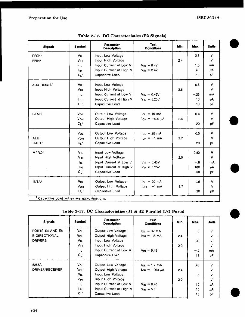
Preparation for Use iSBC 80/24A
Table 2-16. DC Characteristics (P2 Signals)
Signals Symbol Parameter Test Min. Max. Units Description Conditions •
PFSN/ VIL Input low Voltage 0.8 V
PFIN/ VIH Input High Voltage 2.4 V
ilL Input Current at low V VIN = 0.4V -1.6 mA
ilH Input Current at High V VIN = 2.4V 40 p.A
Cll Capacitive load 10 pF
AUX RESET/ VIL Input low Voltage 0.8 V
VIH Input High Voltage 2.6 V
IlL Input Current at low V VIN = 0.45V -.25 mA
IIH Input Current at High V VIN = 5.25V 10 pA Cll Capacitive load 10 pF
BTMO VOL Output low Voltage IOL = 16 mA 0.4 V
VOH Output High Voltage IOH = -400 pA 2.4 V Cll Capacitive load 20 pF • VOL Output low Voltage IOL = 20 mA 0.5 V
ALE VOH Output High Voltage IOH = -1 mA 2.7 V HAlT/ Cll Capacitive load 20 pF
MPRO/ VIL Input low Voltage 0.80 V
VIH Input High Voltage 2.0 V
IlL Input Current at low V VIN = 0.45V -.6 mA
IIH Input Current at High V VIN = 5.25V 100 pA Cl l Capacitive load 60 pF •
INTA/ VOL Output low Voltage IOL = 20 mA 0.5 V VOH Output High Voltage IOH = -1 mA 2.7 V Cl l Capacitive load 20 pF
1 Capacitive load values are approximations.
Table 2-17. DC Characteristics (Jl & J2 Parallel 1/0 Ports)
Signals Symbol Parameter Test Min. Max. Units Description Conditions •
PORTS E4 AND E8 VOL Output low Voltage IOL = 32 mA .5 V BIDIRECTIONAL VOH Output High Voltage IOH = -5 mA 2.4 V DRIVERS VIL Input low Voltage .90 V
VIH Input High Voltage 2.0 V ilL Input Current at low V VIN = 0.45 -.2 mA Cl l Capacitive load 18 pF
8255A VOL Output low Voltage IOL = 1.7 mA .45 V DRIVER/RECEIVER VOH Output High Voltage IOH = -200 JiA 2.4 V
VIL Input low Voltage .8 V VIH Input High Voltage 2.0 V IlL Input Current at low V VIN = 0.45 10 JiA IIH Input Current at High V VIN = 5.0 10 p.A Cl l Capacitive load 10 pF •
2-24

iSBCSO/24A
• BCLKI
CBROI
BPRNI
• BUSYI
BPROI
ADDRESS
• WRITE DATA
WRITE COMMAND
WRITEXACK
• READ COMMAND
READ DATA
READXACK
•
Preparation for Use
IBey~ r-IBW-4 H r-IBW
----~r~~I __________________ ~/---------~~\I" C--------,
~~~--IDBy------~----~
J I ,-------{----~ ~INOD
\~-------------------------.:JI'" f~ ____________ S_TA_B_L_E_A_D_DR_E_S_S ________ __J)( ~
____ ~~ \~ _____________ S_TA_B_L_E_D_AT_A __________ ~)( ~ lAS. IDS--..j r- ~I r-IAH.IDHW
' ... 4-------leIlDW-----___ )o-l' \ 7
~ \ ... \
lellDR ~I , IDXL~ r-
Figure 2-3. System Timing Diagram
t l-IXKH
2-25

Preparation for Use
2-19. BOARD PRIORITY RESOLUTION
Your iSBC 80/24A board has been designated as a "Full Master" board. This means the board is equipped with bus-arbitration logic and can acquire and relinquish control of the common system Multibus lines (see section 4-33). In order for this system to be effective, a board priority scheme needs to be established in your system.
If your iSBC 80/24A board is the only master in the system, it should be placed in the top slot (J2) of the iSBC 604/614 Cardcage. Normally, pin 15 (BPRN/) of the iSBC 604/614 backplane connector J2 is grounded with jumper B-N. However, this connection should be verified. This will allow the other three slots to be used for any expansion boards or for future master boards.
When using the iSBC 80/24A board in a multimaster system, a priority resolution scheme must be established. Two methods of priority are possible: a serial (daisy chain) method; or a parallel method.
Another important consideration in setting up a multi-master system is the Multibus clock signal
15 ~
B(
N
-
HIGHEST PRIORITY MASTER
J2
BPRN/
BPROI
16 <>--
J3
15 BPRNI r-<l
BPROI
~
Co
Ml
--
iSBC80/24A
source. You must ensure only one master board is supplying the BCLKI & CCLKI signals to the Multibus lines. All master boards have provisions for disabling the output of these two signals (i.e., preventing the signals from going off-board). Refer to the schematic diagrams of the particular master board, in your hardware reference manual.
2-20. SERIAL PRIORITY
Serial priority is implemented by board placement. If your iSBC board resides in slot J2, as previously described, the next lower priority will be assigned to slot J3. Slot J4 will have the lowest priority in this scheme. Due to the propagation delay of the BPROI signal path, this scheme is limited to a maximum of three master boards. In the configuration shown in figure 2-4, the master board installed in slot J2 has the highest priority and is able to acquire control of the Multibus lines any time the bus is not busy, since the BPRNI input is always true (tied to ground via jumper connections B-N on the iSBC 6041614 Backplane).
If the master board in slot J2 desires control of the M ultibus lines, it drives its BPRO 1 output high (false)
~
~
~
EO
Ll
--
LOWEST PRIORITY MASTER
J4
BPRNI
BPROI
BPRO/AN NOTUSED MASTERS.
~6\
He>
Kl -
o SPRNI PINS BY NON-
iSBC® 604 BACKPLANE
(BOTTOM)
Figure 2-4. Serial Priority Resolution Scheme
2-26
•
•
•
•
•

•
•
•
•
•
iSBC 80/24A
and inhibits the BPRNI inputs to the remaining lower priority master boards. The master board then takes control of the Multibus lines when the current bus cycle is completed. When finished using the Multibus lines, the J2 master board pulls its BPROI output low (true) and gives the J3 master board the opportunity to acquire Multibus line control. IftheJ3 master board does not want the Multibus lines, it pulls its BPROI output low (true) and gives the J4 master board the opportunity to assume control of the Multibus lines.
To implement the serial priority scheme in your own custom chassis, wire the BPRO 1 and BPRN 1 signals as shown in figure 2-4. Slots between masters may be left empty by installing a jumper between JI-15 and JI-16 on the empty slot.
2-21. PARALLEL PRIORITY RESOLUTION
A parallel priority resolution scheme allows up to 16 bus masters to acquire and control the Multibus lines. Figure 2-5 illustrates one method of implementing such a scheme for resolving bus contention in a system containing eight bus masters installed in two iSBC 604/614 Cardcages. Notice that the two highest
NO.1 NO.2 PRIORITY
PRIORITY (HIGHEST) J2 J3
~ BPRN/ ~ BPRN/
(NOTE) (NOTE)
BREQ/ p.!!- BREQ/ p..!!-
.J!.o
Preparation for Use
and two lowest priority bus masters are shown installed in the iSBC 604 Cardcage.
In the scheme shown in figure 2-5, the priority encoderis a Texas Instruments 74148 and the priority decoder is an Intel 8205. Input connections to the priority encoder determine the bus priority, with input 7 having the highest priority and input 0 having the lowest priority. Here, the J3 bus master has the highest priority and theJ5 bus master has the lowest priority.
IMPORTANT: In a parallel priority resolution scheme, the BPROI output must be disabled on all bus masters. On the iSBC 80/24A board, disable the BPROI output signals by removing jumper E200-201. If a similar jumper cannot be removed on the other master boards, either clip the IC pin that supplies the BPROI output signal to the Multibus connector or cut the signal trace.
2-22. POWER-FAIL/BATTERY BACKUP PROVISIONS
The iSBC 80/24A board has provisions for interrupting the CPU in the event of a system power
NO.8 NO.7 PRIORITY
PRIORITY (LOWEST) J4 J5
BPRN/ ~ BPRN/
(NOTE) (NOTE)
BREQ/ p1!- BREQ/ po.!!.
,- - - - - - I- I-- - - - - - - - - - - - I- - - - - - -f- -'1 B~g;;~~E I ( B A C D E F H G (BOTTOM)
L_ -----f-I-------.- -----1- 1-------
NOTE: REFER TO TEXT REGARDING THE DISABLING OF BPRO/ OUTPUT.
BUS PRIORITY
RESOLVER
Figure 2-5. Parallel Priority Resolution Scheme
_J
2-27
Preparation for Use
failure, maintaining power-fail status, and providing user-supplied battery backup over the P2 connector for the RAM in the event of a drop in power.
The Power-Fail Interrupt signal (PFINI) is received at connector pin P2-19 and clocks the Power-Fail Interrupt latch at U15. The output from this latch can be connected to the PIC, via the interrupt jumper matrix. When an output instruction to port D4 is executed, the Power-Fail Interrupt latch is reset.
A Power-Fail Status signal (PFSNI) is received at connector pin P2-17. When an input instruction to port D4 is executed, the level on PFSNI is input on the least significant data bus line (DBO). The Power-Fail Status signal is generated by your own off-board power-fail circuitry. This alows your main program to differentiate between power coming back up from a power failure or power being initially turned on. In other words, the program can tell whether to restart to where it left off or to initialize the system.
Connector pins P2-3 and 4 can be connected to a + 5 Vdc back-up battery that will provide power to your iSBC 80/24A RAM in the event of a power failure. Refer to table 1-1 for battery current requirements. Jumper pair E216-217 must be disconnected when the battery back-up feature is used. Refer to figures 5-3 and 5-4, sheet 1.
The Memory Protect (MPROI) signal is received at connector pin P2-20 and is ANDed with PROM ACKI through U38 and then applied to the CE2 input (pin 26) of RAM device U51. This signal is used to prevent she spurious signals, which may be generatd on the memory command lines during power going down, from affecting the contents of memory. When MPROI is true (low; 0 volts) the RAM devices will be powered down and disabled.
The PFSRI signal (Power-Fail Sense Reset) is used to reset the ACLO flip-flop, which is an external circuit used to trigger the PFINI (power-fail interrupt) signal. Typically, the ACLO flip-flop is triggered when AC line voltage falls below 90% of its nominal value. Refer to table 2-4 for instructions on implementing the PFSRI jumper, which is enabled by parallel port circuity.
The following is a typical example of how the various power-fail signals could be used:
a. A power failure occurs. When the AC line voltage reaches some predetermined level (-10% typically) the power-fail circuitry generates a Power-Fail Interrupt (PFIN/) signal.
b. The CPU is interrupted and goes into a program status saving routine. The routine should end with a HALT instruction.
2-28
iSBC 80/24A
c. After a user-determined length of time (5 ms for example) the power-fail circuitry should generate Memory Protect (MPRO/) signal.
d. DC power goes down.
e. AC power returns. The power-fail circuitry should generate a SYSTEM RESET signal and hold it until the power supplies are stable. Reset should also be held until the MPROI signal is cleared.
f. The system program can now read the Power-Fail Status signal and determine what type of restart procedure is to be executed.
For additional information on power-fail schemes for Intel Single Board Computers, refer to the Intel Multibus Specification.
2·23. PARALLEL 1/0 CABLING
Parallel I/O ports E4, E5 and E6 are controlled by the PPI device in socket U15, and are interfaced via edge connector J1. Similarly, parallel I/O ports E8, E9 and EA are controlled by the PPI device in socket U17 and are interfaced via edge connector J2.
Pin assignments for Jl and J2, in the factory default configuration, are listed in tables 2-18 and 2-19 respectively. Bit order for ports E6 and EA may be altered by jumper connection. Refer to section 2-14 for instructions. DC characteristics of the parallel I/O signals are listed in table 2-17. Connector information for Jl and J2 is provided in table 2-9.
The transmission path from the I/O source to the iSBC 80/24A board should be limited to 3 meters (10 feet).
An Intel iSBC 956 Cable Set, consisting of two cable assemblies is recommended for parallel I/O interfacing.
Both cable assemblies consist of a 50-conductor flat cable with a 50-pin PC connector at one end. When attaching the cable to Jl or J2, be sure that the connector is oriented properly with respect to pin 1 on the edge connector. (Refer to the footnotes in tables 2-18 and 2-19.)
The following bulk cable types (or equivalent) are recommended for interfacing with the parallel 1/0 ports:
a. 50-conductor flat cable, 3M 3365-50.
b. 50-conductor flat cable (with ground plane), 3M 3469-50
c. 25-pair flat-twisted cable, Belden 9V28050.
•
•
•
•
•

•
•
•
•
•
iSBC80/24A
Table 2-18. Connector Jl Pin Assignments
Pin Signal Pin Signal
1 GND 2 PORT E5 - BIT 7
3 GND 4 PORT E5 - BIT 6
5 GND 6 PORT E5 - BIT 5
7 GND 8 PORT E5 - BIT 4
9 GND 10 PORT E5 - BIT 3
11 GND 12 PORT E5 - BIT 2
13 GND 14 PORT E5 - BIT 1
15 GND 16 PORT E5 - BIT 0
17 GND 18 PORT E6 - BIT 3
19 GND 20 PORT E6 - BIT 2
21 GND 22 PORT E6 - BIT 1
23 GND 24 PORT E6 - BIT 0
25 GND 26 PORT E6 - BIT 4
27 GND 28 PORT E6 - BIT 5
29 GND 30 PORT E6 - BIT 6
31 GND 32 PORT E6 - BIT 7
33 GND 34 PORT E4 - BIT 7
35 GND 36 PORT E4 - BIT 6
37 GND 38 PORT E4 - BIT 5
39 GND 40 PORT E4 - BIT 4
41 GND 42 PORT E4 - BIT 3
43 GND 44 PORT E4 - BIT 2
45 GND 46 PORT E4 - BIT 1
47 GND 48 PORT E4 - BIT 0
49 GND 50 EXTERNAL INTERRUPT
OR + 5V OR OPEN
NOTES: 1. All odd-numbered pins are on the component side of
the board. Pin 1 is rightmost when board is viewed with 1/0 connectors on top.
2. Cable connector numbering convention may not agree with board edge connector numbering.
2-24. SERIAL 1/0 CABLING
Pin assignments and signal names for connector J3 (serial I/O interface) are listed in table 2-20. An Intel iSBC 955 Cable Set is recommended for RS232C interfacing. One cable assembly (in the set) consists of a 25-conductor flat cable with a 26-pin PC connector at one end and an RS232C interface connector at the other end. The other cable assembly includes an RS232C connector at one end and has spade lugs at the other end; the spade lugs are used to interface to a teletypewriter .
For OEM applications where cables will be made for the iSBC 80/24A board, it is important to note
Preparation for Use
Table 2-19. Connector J2 Pin Assignments
Pin Signal Pin Signal
1 GND 2 PORT E9 - BIT 7
3 GND 4 PORT E9 - BIT 6
5 GND 6 PORT E9 - BIT 5
7 GND 8 PORT E9 - BIT 4
9 GND 10 PORT E9 - BIT 3
11 GND 12 PORT E9 - BIT 2
13 GND 14 PORT E9 - BIT 1
15 GND 16 PORT E9 - BIT 0
17 GND 18 PORT EA - BIT 3
19 GND 20 PORT EA - BIT 2
21 GND 22 PORT EA - BIT 1
23 GND 24 PORT EA - BIT 0
25 GND 26 PORT EA - BIT 4
27 GND 28 PORT EA - BIT 5
29 GND 30 PORT EA - BIT 6
31 GND 32 PORT EA - BIT 7
33 GND 34 PORT E8 - BIT 7
35 GND 36 PORT E8 - BIT 6
37 GND 38 PORT E8 - BIT 5
39 GND 40 PORT E8 - BIT 4
41 GND 42 PORT E8 - BIT 3
43 GND 44 PORT E8 - BIT 2
45 GND 46 PORT E8 - BIT 1
47 GND 48 PORT E8 - BIT 0
49 GND 50 EXTERNAL INTERRUPT OR + 5V OR OPEN
NOTES: 1. All odd-numbered pins are on the component side of
the board. Pin 1 is rightmost when board is viewed with 1/0 connectors on top.
2. Cable connector numbering convention may not agree with board edge connector numbering.
that the mating connector for J3 has 26 pins whereas the RS232C connector has 25 pins. Consequently, when connecting the 26-pin mating connector to 25-conductor flat cable, be sure that the cable makes contact with pins 1 and 2 ofthe mating connector and not with pin 26. Table 2-21 provides pin correspondence between connector J3 and an RS232C connector. When attaching the cable to J3, be sure that the PC connector is oriented properly with respect to pin 1 on the edge connector. (Refer to the footnote in table 2-20.)
If your application requires a 20 mA current loop (TTY) interface refer to section 2-25.
2-29

Preparation for Use iSBC 80/24A
Table 2-20. Connector J3 Pin Assignments
Pin Signal Pin Signal
1 SECONDARY TRANSMITTED DATA 2 PROTECTIVE GROUND
3 TRANSMITTER SIGNAL ELEMENT TIMING 4 TRANSMITTED DATA
5 SECONDARY RECEIVED DATA 6 RECEIVED DATA
7 RECEIVER SIGNAL ELEMENT TIMING 8 REQUEST TO SEND
9 NOT USED BY RS232 10 CLEAR TO SEND
11 SECONDARY REQUEST TO SEND 12 DATA SET READY
13 DATA TERMINAL READY 14 SIGNAL GROUND
15 NOT USED BY RS232 16 RECEIVED LINE SIGNAL DETECT
17 RING INDICATOR 18 NOT USED BY RS232
19 -12V (TTY ADAPTER POWER) 20 NOT USED BY RS232
21 TRANSMITTER SIGNAL ELEMENT TIMING 22 +12V (TTY ADAPTER POWER)
23 +5V 24 NOT USED BY RS232
25 SIGNAL GROUND 26 SECONDARY CLEAR TO SEND
NOTES: 1. All odd-numbered pins are on the component side of the board. Pin 1 is rightmost when board is viewed with I/O
connectors on top. 2. Cable connector numbering convention may not agree with board connector numbering.
Table 2-21. Connector Pin Correspondence (25-Pin to 26-Pin)
Signal Name Pin J3 25-Pln
Connector
Protective Ground 2 1
Secondary Transmitted Data 1 14
Transmitted Data 4 2
Transmitter Signal Element Timing 3 15
Received Data 6 3
Secondary Received Data 5 16
Request to Send 8 4
Receiver Signal Element Timing 7 17
Clear to Send 10 5
(No connection) 9 18
Data Set Ready 12 6
Secondary Request to Send 11 19
Signal Ground 14 7
Data Terminal Ready 13 20
Received Line Signal Detect 16 8
(No connection) 15 21
(No connection) 18 9
Ring Indicator 17 22
(No connection) 20 10
TTY Adapter Power (-12V) 19 23
TTY Adapter Power (+12V) 22 11
Transmitter Signal Element Timing 21 24
(No connection) 24 12
(+5V) 23 25
Secondary Clear to Send 26 13
Signal Ground 25 No Connection
2-30
2·25. CURRENT LOOP (TTY) INTERFACE
'lb adapt your iSBC 80/24A board to a 20 mA current loop (TTY) interface, optional jumper connections are required. In addition, the iSBC 530 Teletypewriter Adaptor module must be installed between the board and the serial peripheral. The necessary jumper connection are as follows:
Install jumper E75-80 (provides -12V to module)
Install jumper E78-79 (provides + 12V to module)
Current limiting is not provided for these outputs. If improperly connected, damage to the board and power supply could result.
Refer to figure 5-3 for jumper post locations, and figure 5-4, sheet 7 for schematic drawing. Connector J3 pin assignments are listed in table 2-21.
The optional TTY interface module (iSBC 530 Teletypewriter Adapter) converts iSBC 80/24A RS232C signal levels to an optically isolated 20 mA current loop interface and provides signal translation for transmitted data, received data and a teletypewriter paper tape reader relay.
•
•
•
•
•

•
•
•
•
•
iSBC80/24A
2-26. MULTIMODULETM BOARDS AND THE iSBXTM BUS
The iSBC 80/24A board is equipped with two iSBX (single board expansion) bus connectors (J5 and J6). This bus allows on-board 110 expansion, using optional iSBX Multimodule boards. Connectors J5 and J6 may be used only for iSBX Multimodule boards. Table 2-22 provides the iSBX bus connector pin assignments, and table 2-22A provides iSBX signal descriptions. Each of the two connectors has identical pin assignments, and physical layout.
For installation instructions, refer to the specific iSBX Multimodule board hardware reference manual. When a Multimodule board is installed, the iSBC 80/24A board's power requirement will increase by the amount specified in the Multimodule board manual.
Preparation for Use
2-27. FINAL INSTALLATION
I~ Always turn off the computer system power supply before installing or removing the iSBC 80/24A board and before installing or removing interface cables. Failure to take these precautions can result in damage to the board.
In an iSBC Single Board Computer based system, install the iSBC 80/24A board in any slot that has not been wired for a dedicated function. In an Intellec 800 System, install the iSBC 80/24A board in any slot except slot 1 or 2 (slots 1 and 2 are reserved). Ensure auxiliary edge connector P2 (if used) is correctly inserted. Attach the appropriate cable assembles to connectors Jl through J3, and any Multimodule board connectors .
Table 2 22 iSBXTM Bus Connector Pin Assignments - . Pin
35
33 31
29 27
25
23
21 19
17
15
13
11
9 7
5
3
1
10RDI
10WRTI
MRESETI
MCSOI
MCS11
MAG-2
MPSTI
MINTRO-1
MWAITI
MCLKI
OPTO-1
MDO-7
Mnemonic Description Pin Mnemonic
GND SIGNAL GROUND 36 +5V
MDO MDATA BIT 0 34 -MD1 MDATA BIT 1 32 -
MD2 MDATA BIT 2 30 OPTO
MD3 MDATA BIT 3 28 OPT1
MD4 MDATA BIT 4 26 -MD5 MDATA BIT 5 24 -MD6 MDATA BIT 6 22 MCSOI
MD7 MDATA BIT 7 20 MCS11
GND SIGNAL GROUND 18 +5V
10RDI 10 READ COMMAND 16 MWAITI
10WRTI 10 WRITE COMMAND 14 MINTRO
MAO M ADDRESS 0 12 MINTR1
MA1 M ADDRESS 1 10 -MA2 M ADDRESS 2 8 MPSTI
MRESET M RESET 6 MCLK
GND SIGNAL GROUND 4 +5V
+12V +12 Volts 2 -12V
Table 2-22A. iSBXTM Bus Signal Descriptions
Commands the Multimodule board to perform the read operation.
Commands the Multimodule board to perform the write operation. Initializes the Multimodule board to a known internal state.
Description
+5 Volts
RESERVED
RESERVED
OPTION 0
OPTION 1
RESERVED
RESERVED
M CHIP SELECT 0
M CHIP SELECT 1
+5 Volts
M WAIT
M INTERRUPT 0
M INTERRUPT 1
RESERVED
M PRESENT M CLOCK
+5 Volts -12 Volts
Chip select. Selects 1/0 addresses CG-C7 on the J5 Multimodule board and addresses FG-F7 on the J6 Multimodule board.
Chip select. Selects 1/0 addresses C8-CF on the J5 Multimodule board and addresses F8-FF on the J6 Multimodule board.
Least three bits of the I/O address. Used in conjunction with the chip select and command lines. Multimodule present indicator. Informs iSBC 80/24A board that a Multimodule board(s) is installed.
Interrupt request lines from the Multimodule board to the iSBC 80/24A board interrupt matrix.
Causes iSBC 80/24A board to execute wait states until Multimodule board is ready to respond.
9.68 MHz Multimodule board timing reference from iSBC 80/24A board.
Optional use lines. May be used for additional interrupt request lines. Bidirectional data lines.
* * * 2-3112-32

•
•
•
•
•

•
•
•
•
•
CHAPTER 3 PROGRAMMING INFORMATION
3-1. INTRODUCTION
Several Intel programmable devices reside on the iSBC 80/24A board. This chapter provides programming information for these devices and gives typical examples for most applications. Memory and I/O addressing are provided in table form for quick reference.
3-2. MEMORY ADDRESSING
The iSBC 80/24A board can accommodate up to 32K bytes of ROM/EPROM on-board. Four sockets are provided for these devices. Table 3-1 lists the address ranges for the type of ROM/EPROM installed (lK, 2K, 4K, or 8K). The factory configuration for 2764-type devices (8K bytes each) indicates an on-board ROM/EPROM address range from 0000-7FFF (hexadecimal).
In the factory configuration, 8K bytes of RAM reside on-board. RAM addressing in this configuration is assigned from EOOO to FFFF (hexadecimal). RAM addressing in optional configurations will depend on the amount of ROMIEPROM installed onboard. Table 3-2 summarizes these RAM address options.
Table 3-1. EPROM/ROM Memory Size
Quantity of Address Device EPROMs/ROMs Installed' Range Type 1 2 3 4 (Hex)
270B,275B 1K 2K 3K 4K OOOO-OFFF 260B
2716 2K 4K 6K BK 0000-1 FFF
2316E
2732,2732A 4K BK 12K 16K 0000-3FFF
2764,2764A BK 16K 24K 32K 0000-7FFF
'EPROM/ROM types cannot be mixed.
If non-existent memory is addressed, the on-board failsafe timer will expire in approximately 10 milliseconds sending an acknowledge signal to the CPU so that it may resume processing. For failsafe timer jumper information refer to section 4-35, and table 2-4.
Table 3-2. On-Board RAM Address Space (Hexadecimal)
Max. RAM Jumper 2K 4K 8K
E112-113 3BOO-3FFF 3000-3FFF 2000-3FFF
E111-112 7BOO-7FFF 7000-7FFF 6000-7FFF
E103-104 BBOO-BFFF BOOO-BFFF AOOO-BFFF
E102-103* FBOO-FFFF FOOO-FFFF EOOO-FFFF*
* Default configuration.
When the CPU is addressing on-board memory (ROMIPROM or RAM) an internal PROM or RAM Acknowledge (ACK/) is automatically generated to prevent imposing a CPU wait state. When the CPU is addressing system memory via the Multibus lines, the CPU must first gain control of the Multibus lines and, after the Memory Read or Memory Write Command is given, must wait for a Transfer Acknowledge (XACK/) to be received from the addressed memory device.
3-3. I/O ADDRESSING
The on-board 8085A-2 CPU communicates with the programmable devices through a sequence of I/O read and I/O write commands. Each device has a specific, fixed (dedicated) address, or group of addresses, through which commands and data are issued and accepted. All of these fixed on-board I/O addresses are listed in table 3-3. In addition to the board's programmable I/O devices, certain other functions have specific addresses assigned to them. These addresses are also included in the table.
3-4 SYSTEM INITIALIZATION
When power is initially applied to the system, the initialize (INIT!) signal is automatically generated by the 8224 Clock Generator. This clears the internal program counter, instruction register, and the interrupt enable flip-flop circuit of the CPU. The INIT/ signal also resets the 825lA Programmable Communication Interface (PCl) device and the two 8255A PPI devices as follows:
a. The 8251A PCI is set to an "idle" mode, waiting for a set of command words to program the desired function.
3-1

Programming Information iSBC 80/24A
Table 3-3. 1/0 Port Addressing
I/O Port Address I/O Device Input Function Output Function (hexadecimal)
04 Power Fail Read Power Fail Status Reset Power Fail Latch
05 System Bus Override Not used Set or reset override control (using data bus line 0).
06 LED Diagnostic Indicator Not used Flash LED for 1 millisecond
07 Reserved - -
08 or DA 8259A Interrupt Controller
Various Read Functions Various Write Functions 09 or DB Refer to section 3-36 Refer to section 3-36
DC Read counter 0 Load counter 0 DO Read counter 1 Load counter 1 DE 8254 Interval Timer Read counter 2 Load counter 2
(Baud Rate Generator) OF Read Status Mode control
E4 Read port A Write port A E5 8255A at U15 J1 Read port B Write port B E6 Read port C Write port C E7 - Control
E8 Read port A Write port A E9 Read port B Write port B
8255A at U17 J2 EA Read port C Write port C EB - Control
EC or EE 8251A J3
Data in Data out ED or EF Read Status Control
CO-C7 Multimodule 1 MCSO/ } J5 C8-CF Multimodule 1 MCS11
Various Read Functions Various Write Functions FO-Ff Multimodule 2 MCSO/ } F8-FF Multimodule 2 MCS11
J6
Note: When either Multimodule is present, the 1/0 ports CG-FF are dedicated.
b. All three ports of each 8255A PPl device are set to Mode 0, input.
The lNlT / signal is also gated to other boards in the system, via the Multibus lines, to set all components to a known internal condition. The lNlT / signal can also be generated by an auxiliary reset switch, such as on the iSBC 655 System Chassis front panel. Pressing and releasing the switch produces the same effect previously described.
3-5. 8254 PROGRAMMABLE INTERVAL TIMER (PIT) PROGRAMMING
Each of the three counters (Counter 0, Counter 1, and Counter 2) can use either the on-board 2.15 MHz oscillator, or an external clock input (D.C. to 10 MHz) from Port E6. The factory set jumpers select the on-board 2.15 MHz reference; refer to table
3-2
for these jumper settings, and the jumpers required to select the external references.
Default jumpers connect the O2 output of the counter to the on-board PCl device. The other two outputs are routed to the interrupt matrix. The 0, output is also routed to the port E6 jumper matrix. Refer to table 2-5.
3-6. MODE CONTROL WORD AND COUNT
All three counters must be initialized separately prior to their use. The initialization for each counter consists of two steps:
a. A mode control word (figure 3-1) is written to the control register for each individual counter.
b. A down-count number is loaded into each counter. One or two bytes must be sent to the PIT, as determined by the mode control word.
•
•
•
•
•
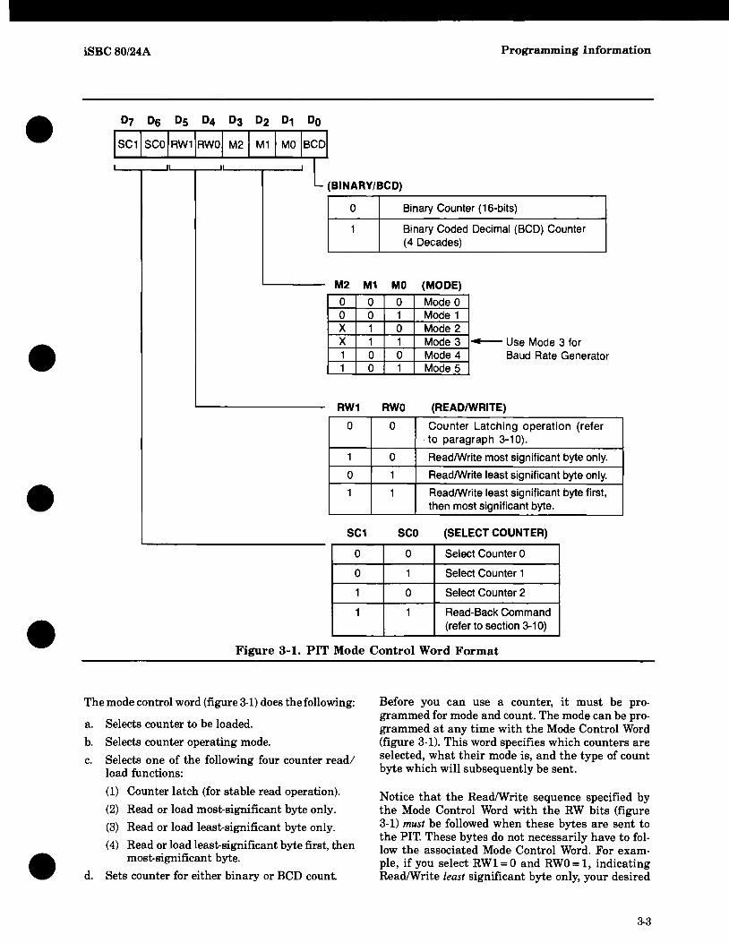
•
•
•
•
•
iSBC 80/24A Programming Information
" (BINARY/BCD)
o Binary Counter (16-bits)
M2 M1
0 0 0 0 X 1 X 1
0 0
RW1
0
1
0
1
SC1
0
0
1
1
Binary Coded Decimal (BCD) Counter (4 Decades)
MO (MODE)
0 Mode 0 1 Mode 1 0 Mode 2 1 Mode 3 ..-- Use Mode 3 for 0 Mode 4 Baud Rate Generator
Mode 5
RWO (READ/WRITE)
0 Counter Latching operation (refer . to paragraph 3-10).
0 Read/Write most significant byte only.
1 Read/Write least significant byte only.
1 Read/Write least significant byte first, then most significant byte.
SCQ (SELECT COUNTER)
0 Select Counter 0
1 Select Counter 1
0 Select Counter 2
1 Read-Back Command (refer to section 3-10)
Figure 3-1. PIT Mode Control Word Format
The mode control word (figure 3-1) does the following:
a. Selects counter to be loaded.
b. Selects counter operating mode.
c. Selects one of the following four counter read/ load functions:
(1) Counter latch (for stable read operation).
(2) Read or load most-significant byte only.
(3) Read or load least-significant byte only.
(4) Read or load least-significant byte first, then most-significant byte .
d. Sets counter for either binary or BCD count.
Before you can use a counter, it must be programmed for mode and count. The mode can be programmed at any time with the Mode Control Word (figure 3-1). This word specifies which counters are selected, what their mode is, and the type of count byte which will subsequently be sent.
Notice that the ReadlWrite sequence specified by the Mode Control Word with the RW bits (figure 3-1) must be followed when these bytes are sent to the PIT. These bytes do not necessarily have to follow the associated Mode Control Word. For example, if you select RWI = 0 and RWO = 1, indicating ReadlWrite least significant byte only, your desired
3-3
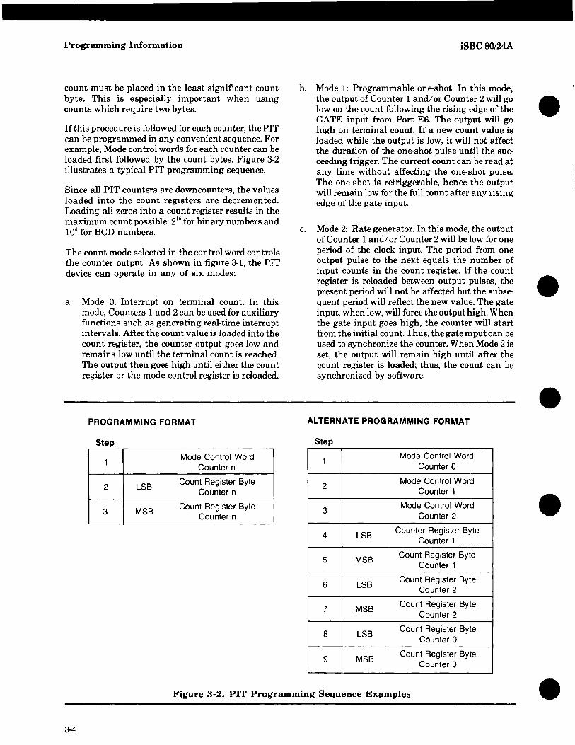
Programming Information
count must be placed in the least significant count byte. This is especially important when using counts which require two bytes.
If this procedure is followed for each counter, the PIT can be programmed in any convenient sequence. For example, Mode control words for each counter can be loaded first followed by the count bytes. Figure 3-2 illustrates a typical PIT programming sequence.
Since all PIT counters are down counters, the values loaded into the count registers are decremented. Loading all zeros into a count register results in the maximum count possible: 216 for binary numbers and 104 for BCD numbers.
The count mode selected in the control word controls the counter output. As shown in figure 3-1, the PIT device can operate in any of six modes:
a. Mode 0: Interrupt on terminal count. In this mode, Counters 1 and 2 can be used for auxiliary functions such as generating real-time interrupt intervals. After the count value is loaded into the count register, the counter output goes low and remains low until the terminal count is reached. The output then goes high until either the count register or the mode control register is reloaded.
PROGRAMMING FORMAT
Step
1 Mode Control Word
Counter n
2 LSB Count Register Byte
Counter n
3 MSB Count Register Byte
Counter n
iSBC 80/24A
b. Mode 1: Programmable one-shot. In this mode, the output of Counter 1 and/or Counter 2 will go low on the count following the rising edge of the GATE input from Port E6. The output will go high on terminal count. If a new count value is loaded while the output is low, it will not affect the duration of the one-shot pulse until the succeeding trigger. The current count can be read at any time without affecting the one-shot pulse. The one-shot is retriggerable, hence the output will remain low for the full count after any rising edge of the gate input.
c. Mode 2: Rate generator. In this mode, the output of Counter 1 and/or Counter 2 will be low for one period of the clock input. The period from one output pulse to the next equals the number of input counts in the count register. If the count register is reloaded between output pulses, the present period will not be affected but the subsequent period will reflect the new value. The gate input, when low, will force the output high. When the gate input goes high, the counter will start from the initial count. Thus, the gate input can be used to synchronize the counter. When Mode 2 is set, the output will remain high until after the count register is loaded; thus, the count can be synchronized by software.
ALTERNATE PROGRAMMING FORMAT
Step
1 Mode Control Word
Counter 0
2 Mode Control Word Counter 1
3 Mode Control Word
Counter 2
4 LSB Counter Register Byte
Counter 1
5 MSB Count Register Byte
Counter 1
6 LSB Count Register Byte
Counter 2
7 MSB Count Register Byte
Counter 2
8 LSB Count Register Byte
Counter 0
9 MSB Count Register Byte
Counter 0
Figure 3-2. PIT Programming Sequence Examples
3-4
•
•
•
•
•

•
•
•
•
•
iSBC 80/24A
d. Mode 3: Square wave generator. Mode 3 is the primary operating mode for all three counters on the 8254. In this mode, the counter output remains high until one half ofthe count value in the count register has been decremented (for even numbers). The output then goes low for the other half of the count. If the value in the count register is odd, the counter output is high for (N + 1)/2 counts, and low for (N - 1)/2 counts.
e. Mode 4: Software triggered strobe. After this mode is set, the output will be high. When the count is loaded, the counter begins counting. On terminal count, the output will go low for one input clock period and then go high again. If the count register is reloaded between output pulses, the present count will not be affected, but the subsequent period will reflect the new value. The count will be inhibited while the gate input is low. Reloading the count register will restart the counting for the new value.
f. Mode 5: Hardware triggered strobe. The counter will start counting on the rising edge of the gate input and the output will go low for one clock period when the terminal count is reached. The counter is retriggerable; the output will not go low until the full count after the rising edge ofthe gate input.
Table 3-4 provides a summary of the counter operation versus the gate inputs.
Table 3-4. PIT Counter Operation Vs. Gate Inputs
~ Low
lalus Or Going Rising High Modes Low
0 Disables Enables counting - counting
1 1) Initiates
- counting -2) Resets output
after next clock
2 1) Disab!es counting
Initiates Enables 2) Sets output counting counting high
immediately
3 1) Disables counting
Initiates Enables 2) Sets output counting counting high immediately
4 Disables Enables -counting counting
5 Initiates - -counting
Programming Information
3-7. ADDRESSING
As listed in Table 3-5 the PIT uses four consecutive I/O addresses: DC - DF. Addresses DC, DD, and DE respectively, are used in loading and reading the count in Counters 0, 1, and 2. Address DF is used in writing the mode control word to the desired counter.
Table 3-5. PIT Register Addresses
1/0 CS RD WR Al Ao Activity Address
(hex)
0 1 0 0 0 Load Counter No. 0 DC 0 1 0 0 1 Load Counter No. 1 DD
0 1 0 1 0 Load Counter No.2 DE
0 1 0 1 1 Write Mode Word DF
0 0 1 0 0 Read Counter No. 0 DC 0 0 1 0 1 Read Counter No. 1 DD
0 0 1 1 0 Read Counter No. 2 DE
0 0 1 1 1 No-Operation 3-State DF 1 X X X X Disable 3-STate -
0 1 1 X X No-Operation 3-State -
NOTE: X = Irrelevant Bit
3-8. INITIALIZATION
To initialize the PIT chips, perform the following:
a. Write mode control word for Counter 0 to ODFH. Note that all mode control words are written to ODFH, since the mode control word must specify which counter is being programmed. (Refer to figure 3-1). Table 3-6 provides a sample subroutine for writing a mode control word for Counter O.
b. Assuming the mode control word has selected a 2-byte load, load least-significant byte of count into Counter 0 at ODCH. Table 3-6 provides a sample subroutine for loading a 2-byte count value.
c. Load most-significant byte of count into Counter Oat ODCH.
NOTE Be sure to enter the downcount in two bytes if the counter was programmed for a twobyte entry in the mode control word. Similarly, enter the downcount value in BCD if the counter was so programmed.
d. Repeat steps a, b, and c for Counters 1 and 2.
Table 3-7 shows another example of a subroutine for writing a mode control word to Counter O.
3-5
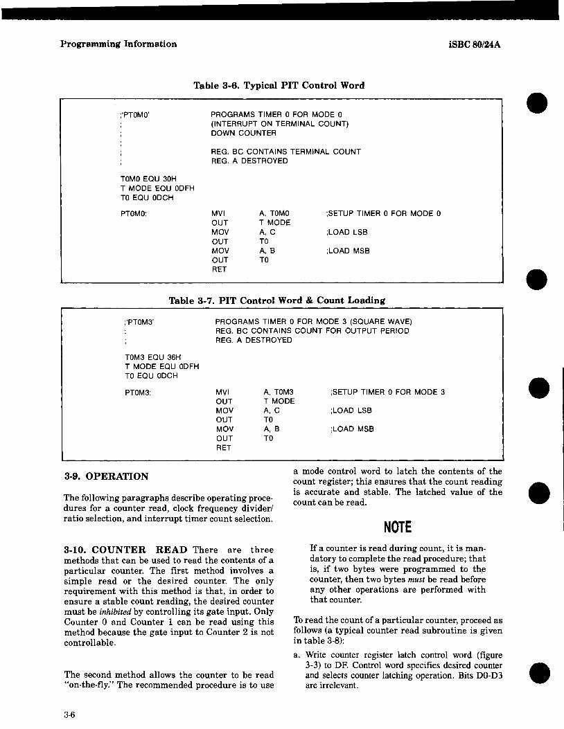
Programming Information iSBC 80/24A
Table 3-6. Typical PIT Control Word
;'PTOMO' PROGRAMS TIMER 0 FOR MODE 0 (INTERRUPT ON TERMINAL COUNT) DOWN COUNTER
REG. BC CONTAINS TERMINAL COUNT REG. A DESTROYED
TOMO EQU 30H T MODE EQU ODFH TO EQU ODCH
PTOMO: MVI OUT MOV OUT MOV OUT RET
A, TOMO T MODE A, C TO A, B TO
;SETUP TIMER 0 FOR MODE 0
;LOAD LSB
;LOAD MSB
Table 3-7. PIT Control Word & Count Loading
;'PTOM3' PROGRAMS TIMER 0 FOR MODE 3 (SQUARE WAVE) REG. BC CONTAINS COUNT FOR OUTPUT PERIOD REG. A DESTROYED
TOM3 EQU 36H T MODE EQU ODFH TO EQU ODCH
PTOM3: MVI OUT MOV OUT MOV OUT RET
A, TOM3 T MODE A, C
;SETUP TIMER 0 FOR MODE 3
;LOAD LSB TO A, B TO
3-9. OPERATION
The following paragraphs describe operating procedures for a counter read, clock frequency divider/ ratio selection, and interrupt timer count selection.
3-10. COUNTER READ There are three methods that can be used to read the contents of a particular counter. The first method involves a simple read or the desired counter. The only requirement with this method is that, in order to ensure a stable count reading, the desired counter must be inhibited by controlling its gate input. Only Counter 0 and Counter 1 can be read using this method because the gate input to Counter 2 is not controllable.
The second method allows the counter to be read "on-the-fly:' The recommended procedure is to use
3-6
;LOAD MSB
a mode control word to latch the contents of the count register; this ensures that the count reading is accurate and stable. The latched value of the count can be read.
NOTE If a counter is read during count, it is mandatory to complete the read procedure; that is, if two bytes were programmed to the counter, then two bytes must be read before any other operations are performed with that counter.
'lb read the count of a particular counter, proceed as follows (a typical counter read subroutine is given in table 3-8):
a. Write counter register latch control word (figure 3-3) to DF. Control word specifies desired counter and selects counter latching operation. Bits DO-D3 are irrelevant.
•
•
•
•
•

•
•
•
•
•
iSBC 80/24A
b. Perform a read operation of desired counter; refer to table 3-5 for counter addresses.
NOTE Be sure to read one or two bytes, whichever was specified in the initialization mode control word. For two bytes, read in the order specified.
D5
0 0
D2 D1 DO
X I X I X I X I I
LDon't Care
Selects Counter Latching Operation
L..-__ Specifies Counter to be Latched
Figure 3-3. PIT Counter Register Latch
Control Word Format
Programming Information
The third method uses the Read-Back Command. This command allows the user to check the count value, programmed Mode, and current status of the OUT pin and Null Count flag of the selected counter(s).
The command is written into the Control Word Register and has the format shown in figure 3-4. The command applies to the counters selected by setting their corresponding bits D3,D2,Dl = 1.
AO, A 1 = 11 CS = 0 RD = 1 WR = 0
I COUNT I STATUS I CNT 21 CNT 1 CNT 0 0
Ds: 0 = LATCH COUNT OF SELECTED COUNTER(S) D4: 0 = LATCH STATUS OF SELECTED COUNTER(S) D3: 1 = SELECT COUNTER 2 D2: 1 = SELECT COUNTER 1 0,: 1 = SELECT COUNTER 0 Do: RESERVED FOR FUTURE EXPANSION: MUST BE 0
m-0394
Figure 3-4. Read-Back Command Format
The read-back command may be used to latch multiple counter output latchs (OL) by setting the COUNT bit D5 = 0 and selecting the desired counter(s). This single command is functionally equivalent to several counter latch commands, one for each counter latched. Each counter's latched count is held until it is read (or the counter is reprogrammed.) That counter is automatically unlatched when read, but other counters remain latched until they are read. If multiple count read· back commands are issued to the same counter
Table 3-8. Typical PIT Counter Read Subroutine
;'RTO'
LT EQU OH T MODE EQU ODFH TO EQU ODCH
RTO:
ALLOWS THE USER TO READ THE COUNT FOR TO ON THE FLY WITHOUT DISTURBING THE COUNT OPERATION REG. A DESTROYED REG. HL WILL RETURN CURRENT COUNT
MVI OUT IN MOV IN MOV RET
A, LT T MODE TO L, A TO H, A
;LATCH TIMER 0 COUNT
;READ TIMER 0 COUNT LSBYTE
;READ TIMER 0 COUNT MSBYTE
3·7

Programming Information
without reading the count, all but the first are ignored; i.e., the count which will be read is the count at the time the first read-back command was issued.
The read-back command may also be used to latch status information of the selected counter(s) by setting STATUS bit D4 = O. Status must be latched to be read; status of a counter is accessed by a read from that counter.
The counter status format is shown in figure 3-5. Bits D5 through DO contain the counter's programmed Mode exactly as written in the last Mode Control Word. OUTPUT bit D7 contains the current state of the OUT pin. This allows the user to monitor the counter's output via software, possibly eliminating some hardware from a system.
0 7 1 = OUT PIN IS 1 o = OUT PIN IS 0
0 6 1 = NULL COUNT
M2
D.
M1
o = COUNT AVAILABLE FOR READING Os-Do COUNTER PROGRAMMED MODE
Figure 3-5. Status Byte
0,
MO BCD
m-0395
NULL COUNT bit D6 indicates when the last count written to the counter register (CR) has been loaded into the counting element (CE). The exact time this happens depends on the MODE of the counter and is described in the Mode Definitions, but until the count is loaded in the counting element (CE), it can't be read from the counter. If the count is latched or read before this time, the count :value will not reflect the new count just written.
If multiple status latch operations of the counter(s) are performed without reading the status, all but the first are ignored; i.e., the status that will be read is that status of the counter at the time the first status read-back command was issued.
Both count and status of the selected counter(s) may be latched simultaneously by setting both COUNT and STATUS bits D5,D4 = O. This is functionally the same as issuing two separate read-back commands at once, and the above discussions apply here also. Specifically, if multiple count and/or status read-back commands are issued to the same counter(s) without any intervening reads, all but the first are ignored.
3-8
iSBC 80/24A
If both count and status of a counter are latched, the first read operation of that counter will return latched status, regardless of which was latched first. The next one or two reads (depending on whether the counter is programmed for one or two type counts) return latched count. Subsequent reads return unlatched count.
For more information on the 8254 PIT device refer to the Intel Microsystem Components Handbook.
3·11. CLOCK FREQUENCY/DIVIDE RATIO SELECTION Table 2-5 lists the default and optional timer input frequencies to Counters 0 through 2. The timer input frequencies are divided by the counters to generate the OITO Interrupt Clock (Counter 0), OIT1 Clock (Counter 1), and the 8251A Baud Rate Clock (Counter 2).
Each counter must be programmed with a downcount number, or count value N. When count value N is loaded into a counter, it becomes the clock divisor. To derive N for either synchronous or asynchronous RS232C operation, use the procedures described in the following paragraphs.
SYNCHRONOUS MODE. In the synchronous mode, the TXC and/or RXC rates equal the Baud rate. Therefore, the count value is determined by
N=C/B
where N is the count value, B is the desired Baud rate, and C is 1.075 MHz, the input clock frequency.
Thus, for a 4800 Baud rate, the required count value (N) is:
N = 1.075 X 106 = 224. 4800
If the binary equivalent of count value N = 224 is loaded into Counter 2, then the output frequency is 4800 Hz, which is the desired clock rate for synchronous mode operation.
ASYNCHRONOUS MODE. In the asynchronous mode, the TXC and/or RXC rates equal the Baud rate times one of the following multipliers: 16 or 64. Therefore, the count value is determined by:
N=C/BM
where N is the count value, B is the desired Baud rate, M is the Baud rate multiplier (16 or 64), and C is 1.075 MHz, the input clock frequency.
•
•
•
•
•

•
•
•
•
•
iSBC 80/24A
Thus, for a 4800 Baud rate, the required count value (N) is:
N = 1.075 X lOb 14 4800 x 16 .
If the binary equivalent of count value N = 14 is loaded into Counter 2, then the output frequency is 4800 X 16 Hz, which is the desired clock rate for asynchronous mode operation. Count values (N) versus rate multiplier (M) for each Baud rate are listed in table 3-9. A simplified version of this table, with hex notations is provided in table 3-10.
NOTE During initialization, be sure to load the count value (N) into the appropriate counter and the Baud rate multiplier (M) into the 8251A PCl.
ISOSYNCHRONOUS MODE. In some cases it is desirable to operate in a hybrid mode which involves transmitting data with the asynchronous format using a synchronous modem. This occurs when a.n increase in operating speed is required without a change in the basic protocol of the system. This hybrid technique is known as isosynchronous and involves the generation of the start and stop bits associated with the asynchronous format, while still using the modem clock for bit synchronization.
In the asynchronous mode the PCI can be programmed to accept clock rates of 16 or 64 times the required baud rate. lsosynchronous operation is a special case of asynchronous with the multiplier rate programmed as one instead of 16 or 64. Note that Xl operation is only valid if the clocks ofthe receiver and transmitter are synchronized.
Table 3-9. PIT Count Values & Rate Multipliers
Baud 1Count Value (N) For Rate (B) M=1 M = 16 M = 64
75 14319 895 224
110 9763 610 153
150 7160 447 112
300 3580 224 56
600 1790 112 28 1200 895 56 14
2400 447 28 7
4800 224 14 -9600 112 7 -
19200 56 - -38400 28 - -
1Count Values (N) assume clock is 1.075 MHz. (N) and Rate Multiplier (M) are in decimal.
Programming Information
Table 3-10. PIT Baud Rate Factors
Output Baud Rate (Hz) 8254 PIT
Baud Rate Frequency Factor (Hex
In kHz Synchronous Asynchronous Notation)
+16 +64 MSB LSB
153.6 - 9600 2400 00 07
76.8 - 4800 1200 DO OE
38.4 38400 2400 600 00 1C
19.2 19200 1200 300 00 38
9.6 9600 600 150 00 70
4.8 4800 300 75 DO EO
2.4 2400 150 - D1 CO
1.76 1760 110 - 02 63
3-12. RATE GENERATORIINTERVALTIMER. Table 3-11 shows the maximum and minimum rate generator frequencies and timer intervals for Counters 0 and 1 when these counters, respectively, have 1.075 MHz and 152.6 KHz clock inputs. The table also provides the maximum and minimum generator frequencies and time intervals a.nd may be obtained by connecting Counters ° and 1 in series.
3-13. INTERRUPT TIMER. To program an interval timer for an interruption terminal count, program the appropriate timer for the correct operating mode (Mode 0) in the control word. Then load the count value (N), which is derived by
N=TC
where N is the count value for Counter 0, T is the desired interrupt time interval in
seconds, and C is the internal clock frequency (Hz).
Table 3-12 shows the count value (N) required for several time intervals (T) that can be generated for Counters ° and 1.
3-14. 8251A PROGRAMMABLE COMMUNICATION INTERFACE (PCI) PROGRAMMING
The PCI converts parallel output data into virtually any serial output data format (including ffiM BiSync) for half. or full-duplex operation. The PCI also converts serial input data into parallel data format.
Prior to transmitting or receiving data, the PCI must be loaded with a set of control words. These control words, which define the complete functional operation of the PCI, must immediately follow a reset (internal or external). The control words are either a Mode instruction or a Command instruction.
3-9
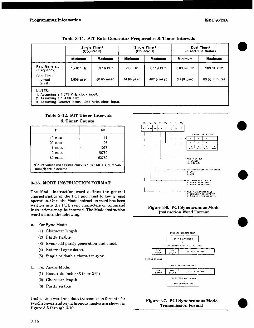
Programming Information iSBCSO/24A
Table 3-11. PIT Rate Generator Frequencies & Timer Intervals
Single Tlmer1 Single Timer" Dual Timer' (Counter 0) (Counter 1) (0 and 1 In Series)
Minimum Maximum Minimum
Rate Generator 16.407 Hz 537.6 kHz 2.05 Hz (Frequency)
Real-Time Interrupt 1.859 lJ.Sec 60.95 msec 14.88 lJ.Sec Interval
NOTES: 1. Assuming a 1.075 MHz clock input. 2. Assuming a 134.38 KHz. 3. Assuming Counter 0 has 1.075 MHz. clock input.
Table 3-12. PIT Timer Intervals & Timer Counts
T N'
10 lJ.Sec 11
100 lJ.Sec 107
1 msec 1075
10 msec 10750
50 msec 53750
1Count Values (N) assume clock is 1.075 MHz. Count Val-ues (N) are in decimal.
3-15. MODE INSTRUCTION FORMAT
The Mode instruction word defines the general characteristics of the PCl and must follow a reset operation. Once the Mode instruction word has been written into the PCl, sync characters or command instructions may be inserted. The Mode instruction word defines the following:
a. For Sync Mode:
(1) Character length
(2) Parity enable
(3) Even/odd parity generation and check
(4) External sync detect
(5) Single or double character sync
b. For Async Mode:
(1) Baud rate factor (X16 or X64)
(2) Character length
(3) Parity enable
Instruction word and data transmission formats for synchronous and asynchronous modes are shown in figure 3-6 through 3-10.
3-10
Maximum Minimum Maximum
67.19 kHz 0.00025 Hz 268.81 kHz
487.8 msec 3.719 lJ.Sec 66.66 minutes
Iscsl,sol EP Ip,,: ',I', I 0 10 1
I
I I
CHARACTER LENGTH
0 1 0 1
0 0 1 1
5 6 7 , BITS BITS 81TS BITS
I
PARITY ENABLE o . ENABLEI (Q - DISABLE)
I
EVEN PARITY GENERATlON/CHEe 1 -= EVEN 0" ODD
I EXTERNAL SYNC DETECT 1 SYNDEr IS AN INPUT o ~ Syt.JDET IS AN OUTPUT
--------~. SINGLE CHARACTER SYNC 1 ~ SINGLE SYNC CHARACTER o· DOUBLE SYNC CHARACTER
Figure 3-6. PCI Synchronous Mode Instruction Word Format
CPU BYTES (5 8 BITS/CHAR)
DATA CHARACTERS
ASSEMBLED SERIAL DATA OUTPUT IT.DI
r---~--,_---~" SYNC SYNC ~
CHAR 1 CHAR 2 DATA CHARACTERS ~~~~~~~---~I~
RECEIVE FORMAT
SERIAL DATA INPUT IRltO)
~ __ ~_~~ __ O_A_TA_C~HAR~~ CPU BYTES (5 8 BITS/CHAR) r----, .... , ----,
DATA CHARACTERS
Figure 3-7. PCI Synchronous Mode Transmission Format
•
•
•
•
•

•
•
•
•
•
iSBC 80/24A
I S, I s, I EP I PlN I" I" I B, I B, I ~ BAUD RATE FACIOR
o 1 0 1 t----~-- --t--
o 0 1 1
.
.
~. -- .-1---~6~~ (IX) 116)(1 (64)(1
CHARACTER LENGTH
0 I 0 I
0 0 1 1
5 6 7 8 BITS BITS BITS BITS
PARITV ENABLE 1 ENABLE 0'" DISABLE
EVEN PARITY GENERATION/CHE 1 EVEN o ~ 000
NUMBER OF STOP BITS
0 1 0 I
0 0 I 1
INVALID 1 1'1, 2 BIT BITS BITS
(ONLY EFFECTS T.II.; Rx NEVER REQUIRES MORE THAN ONE STOP BIT)
Figure 3-8. PCI Asynchronous Mode Instruction Word Format
GENERATED 0001---- o. BY 82S1A
DOES NOT APPEAR
RECEIVER INPUT 0001----0. ON THE DATA BUS
5Y;--' arrs L
t t t t AJIIO 1L._S_TB~~_~T.....JG,--_0_A_T-;A81-'T_S_J.....~_...J 5T6;I
BITS L PROGRAMMED CHARACTER
LENGTH
TRANSMISSION FORMAT
CPu BYTE (58 BITS/CHARI
DATA C~~RACTER ASSEMBLED SERIAL DATA OUTPUT !TxO)
[lATA CHARACTER STO~ L-=---' ___ ....... ___ ....L--.::.;,;,......L_.:j8ITW
RECEIVE FORMAT
SERIAL DATA INPUT (RxO)
DATA CHARACTER STO~ L-_.....J ____ ~~--....L-:.;,;,..---'-~8IT~
CPU BYTE (5-8 BITS/CHAR)' .----~f .. , ----.:....,
DATA CHARACTER L-___ ... , "'"I ___ ...J
'NOTE: IF CHARACTER LENGTH IS DEFINED AS 5, 6 OR 7 BITS THE UNUSED BITS ARE SET TO "ZERO",
Figure 3-9. PCI Asynchronous Mode Transmission Format
Programming Information
TRANSMIT ENABLE 1 ~ enable o ~ disable
DATA TERMINAL READY "high" will force OTR output to lero
RECEIVE ENABLE L----'"'i 1 " enable
o ~ dISable
ERROR RESET 1" reset eHor tlil91
PE, OE, FE
REOUEST TO SENO L-_________ ~I 'high" will loree ffi
output to ItrO
INTERNAL RESET "high" returns 82S1A to Mod. Instruction Format
ENTER HUNT MODe-l : enable selrch fot Sync Chartct."
Figure 3-10. PCI Command Instruction Word Format
3-16. SYNC CHARACTERS
Sync characters are written to the pcr in the synchronous mode only. The pcr can be programmed for either one or two sync characters; the format of the sync characters is at the option of the programmer.
3-17. COMMAND INSTRUCTION FORMAT
The Command instruction word shown in figure 3-10 controls the operation of the addressed PCI. A Command instruction must follow the mode and/or sync words and, once the Command instruction is written, data can be transmitted or received by the PCI.
It is not necessary for a Command instruction to precede all data transactions; only those transactions that require a change in the Command instruction. An exam pIe is a change in the enable transmit bit or enable receive bit. Command instructions can be written to the pcr at any time after one or more data operations .
After initialization, always read the PCI status and check for the TxRDY bit prior to writing either data
3-11

Programming Information
or command words to the PCl. This ensures that any prior input is not overwritten and lost. Note that issuing a Command instruction with bit 6 (IR) set will return the PCl to the Mode instruction format.
3-18. RESET
To change the Mode instruction word, the PCl must receive a Reset command. This can be either a hardware reset or a reset generated by bit 6 of the Command Instruction. The next word written to the PCl after a Reset command is assumed to be a Mode instruction. Similarly, for sync mode, the next word after a Mode instruction is assumed to be one or more sync characters. All control words written into the PCl after the Mode instruction (and/or the sync character) are assumed to be Command instructions.
3-19. ADDRESSING
The PCI device uses two consecutive pairs of addresses. The lower of the two addresses in each pair is used to read and write 110 data; the upper address in each pair is used to write mode and command words and to read the PCl status. (Refer to table 3-13).
Table 3-13. PCI Address Assignments
1/0 Address Command Function Direction (hexadecimal)
ED or EF OUTPUT CONTROL CPU - PCI
EC or EE OUTPUT DATA CPU - PCI
ED or EF INPUT STATUS PCI - CPU
EC or EE INPUT DATA PCI - CPU
3-20. INITIALIZATION
A typical PCI initialization and I/O data sequence is presented in figure 3-11. The PCI device is initialized in four steps:
a. Reset PCI to Mode instruction format.
b. Write Mode instruction word. One function of mode word is to specify synchronous or asynchronous operation.
c. If synchronous mode is selected, write one or two synch characters as required.
d. Write Command instruction word.
To avoid spurious interrupts during PCI initialization, disable the PCI interrupt. This can be done by disabling the CPU interrupts by executing a DI instruction.
3-12
ADDRESS
ED
EO
EO
EO
EC
ED
EC ,
EO
RESET
MODE INSTRUCTION
SYNC CHARACTER 1
SYNC CHARACTER 2
COMMAND INSTRUCTION
DATA 110
COMMAND INSTRUCTION
OATA 110
COMMAND INSTRUCTION
"
-r
iSBC BO/24A
} SYNC MODE
ONLY'
'The second sync character is skipped if Mode instruction has programmed PCI to single character internal sync mode. Both sync characters are skipped if Mode instruction has programmed PCI to async mode.
Figure 3-11. Typical PCI Initialization & Data I/O Sequence
First, reset the PCI device by writing a Command instruction to location ED (or EF). The Command instruction must have bit 6 set (IR6 = 1); all other bits are immaterial.
NOTE This reset procedure should be used only if the PCl has been completely initialized, or if the initialization procedure has reached the point that the PCI is ready to receive a Command word. For example, if the reset command is written when the initialization sequence calls for a sync character, then subsequent programming will be in error.
If the initialization procedure is interrupted, ensure correct reset and programming by writing a series of four command words, with the contents of each word = 00. Then repeat the PCI reset and initialization procedure.
N ext, write a Mode instruction word to the PCl. (See figures 3-6 through 3-9). A typical subroutine for writing both Mode and Command instructions is given in table 3-14.
If the PCI is programmed for the synchronous mode, write one or two sync characters depending on the transmission format.
Finally, write a Command instruction word to the PCL Refer to figure 3-10 and table 3-14.
•
•
•
•
•

•
•
•
•
•
iSBC80/24A Programming Information
Table 3-14. Typical PCI Mode or Command Instruction Subroutine
;CMD2 OUTPUTS CONTROL WORD OR MODE WORD TO PCI. ;USES-STAT; DESTROYS-NOTHING.
CMD2: LP:
3-21. OPERATION
EXTRN STAT
PUSH IN ANI JZ POP OUT RET
END
PSW OEDH 1 LP PSW OEDH
Normal operating procedures use data I/O read and write, status read, and Command instruction write operations. Programming and addressing procedures for the above are summarized in the following paragraphs.
NOTE After the PCI has been initialized, always check the status of the TxRDY bit prior to writing data or writing a new command word to the PCI. The TxRDY bit must be true to prevent overwriting and subsequent loss of command or data words. The TxRDY bit is inactive until initialization has been completed; therefore, do not check TxRDY until after the command word, which concludes the initialization procedure, has been written.
Prior to any operating change, a new command word must be written with command bits changed as appropriate. (Refer to figure 3-10 and table 3-14).
;SAVE DATA AND CPU STATUS ;GET PCI STATUS ;CHECK TXRDY ;TXRDY MUST BE TRUE ;RESTORE DATA AND CPU STATUS: ;SEND COMMAND/MODE WORD TO PCI
For data receive or transmit operations perform a read or write, respectively, to thePCI. Tables 3-15 and 3-16 provide examples of typical character read and write subroutines.
During normal transmit operation, the PCI generates a Transmit Ready (TxRDY) signal that indicates the PCI is ready to accept a data character for transmission. TxRDY is automatically reset when the CPU loads a character into the PCI.
Similarly, during normal receive operation, the PCI generates a Receive Ready (RxRDY) signal that indicates a character has been received and is ready for input to the CPU. RxRDY is automatically reset when a character is read by the CPU.
The TxRDY and RxRDY outputs of the PCI can be used to interrupt the CPU. Refer to section 2-13 for instructions.
The CPU can determine the status of the serial I/O port by issuing an I/O Read Command to the upper address (ED or EF) of the PC! device. The format of the status word is shown in figure 3-12. A typical status read subroutine is given in table 3-17.
Table 3-15. Typical PCI Data Character Read Subroutine
;RX1 READS DATA CHARACTER FROM PCI. ;USES-STAT; DESTROYS-A, FLAGS.
EXTRN STAT
RX1: IN OEDH ANI 2 JZ RX1 IN OECH RET
END
;GET PCI STATUS ;CHECK FOR RXRDY ;RXRDY MUST BE TRUE ;READ DATA FROM PCI
3-13
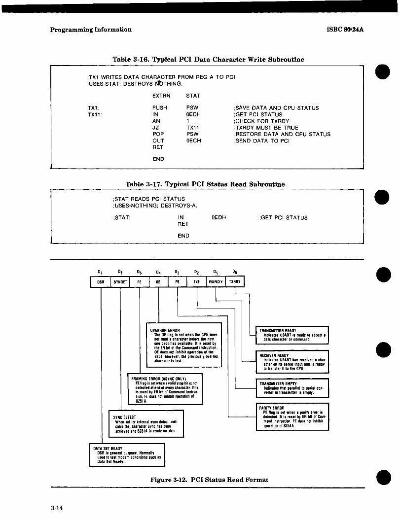
Programming Information iSBC80/24A
3-14
Table 3-16. Typical PCI Data Character Write Subroutine
;TX1 WRITES DATA CHARACTER FROM REG A TO PCI ;USES-STAT; DESTROYS ~THING.
TX1: TX11:
EXTRN
PUSH IN ANI JZ POP OUT RET
END
STAT
PSW OEDH 1 TX11 PSW OECH
;SAVE DATA AND CPU STATUS ;GET PCI STATUS ;CHECK FOR TXRDY ;TXRDY MUST BE TRUE ;RESTORE DATA AND CPU STATUS ;SEND DATA TO PCI
Table 3-17. Typical PCI Status Read Subroutine
;STAT READS PCI STATUS ;USES-NOTHING; DESTROYS-A.
;STAT: IN RET
END
02
OEDH ;GET PCI STATUS
DO
OSR I SYNDET I FE J OE I PE I TXE I RXRDY I TXRDY I I L-
OVERRUN ERROR Y TRANSMITTER READY The DE lIag is set when the CPU does Indicates USART is ready to accept a not read a character belore the next data character or command. one becomes available. It is reset by the ER bit of Ihe Command instruction. DE does not inhibit operation 01 the
RECEIVER READY 8251; however. the previously overrun character is lost. c- Indicates USART has received a char·
acter on Its serial input and is ready to transfer it to the CPU.
FRAMING ERROR (ASYNC ONLY) FE lIag is set when a valid stop bit is not TRANSMITTER EMPTY detected at end 01 every character. 1\ is Indicates that parallel to Slrial can-is reset by ER bit of Command instruc· verter in transmitter Is em ply . lion. FE does not inhibit operation 01 8251A.
PARITY ERROR PE lIag is lit when a parlly IllOr is
SYNC DETeCT detected. It is 1I.lt by ER bit 01 Com-When set lor internal sync detect. indio mand instruction. PE does not inhibit cates that character sync has been operation 01 8251 A. achieved and 8251 A is ready lor data.
DATA SET READY DSR is general purpose. Nonnally used to test modem conditions such as Data Set Ready.
Figure 3·12. PCI Status Read Format
•
•
•
•
•
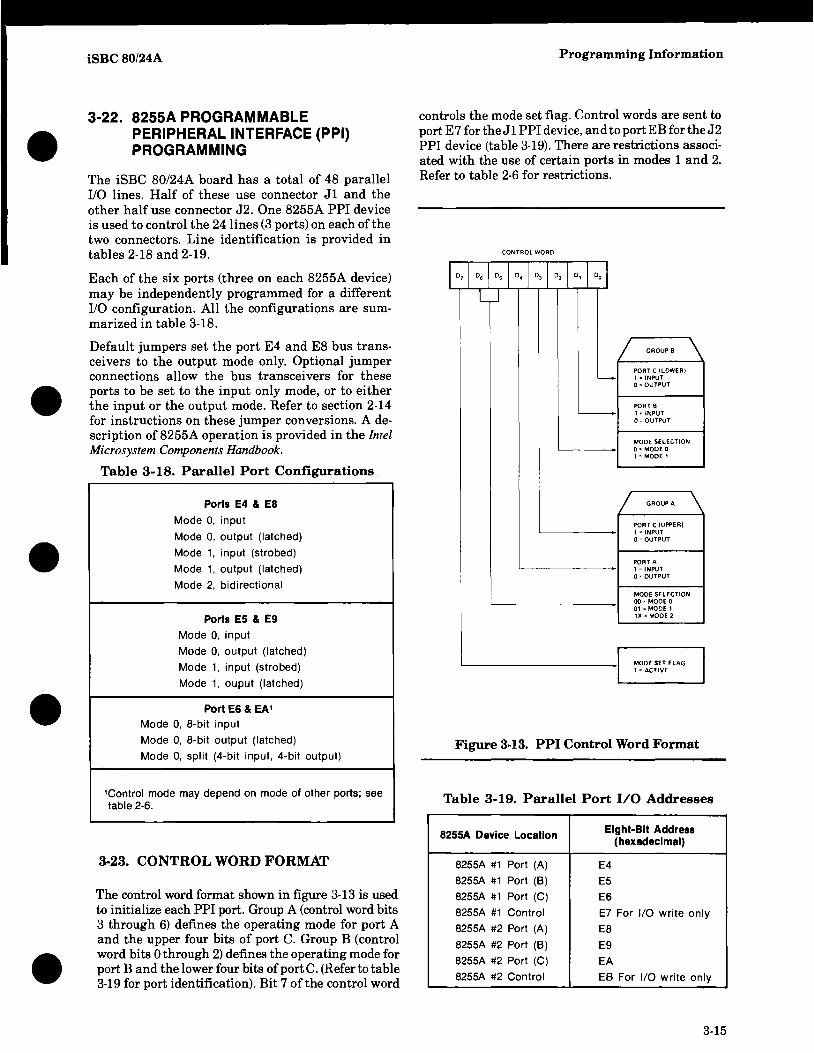
•
•
•
•
•
iSBC 80/24A
3·22. 8255A PROGRAMMABLE PERIPHERAL INTERFACE (PPI) PROGRAMMING
The iSBC 80/24A board has a total of 48 parallel 110 lines. Half of these use connector J1 and the other half use connector J2. One 8255A PPI device is used to control the 24 lines (3 ports) on each of the two connectors. Line identification is provided in tables 2-18 and 2-19.
Each of the six ports (three on each 8255A device) may be independently programmed for a different 110 configuration. All the configurations are summarized in table 3-18.
Default jumpers set the port E4 and E8 bus transceivers to the output mode only. Optional jumper connections allow the bus transceivers for these ports to be set to the input only mode, or to either the input or the output mode. Refer to section 2-14 for instructions on these jumper conversions. A description of 8255A operation is provided in the Intel Microsystem Components Handbook.
Table 3-1B. Parallel Port Configurations
Ports E4 & E8
Mode 0, input
Mode 0, output (latched)
Mode 1, input (strobed)
Mode 1, output (latched)
Mode 2, bidirectional
Ports E5 & E9
Mode 0, input
Mode 0, output (latched)
Mode 1, input (strobed)
Mode 1, ouput (latched)
Port E6 & EAl Mode 0, 8-bit input
Mode 0, 8-bit output (latched)
Mode 0, split (4-bit input, 4-bit output)
lControl mode may depend on mode of other ports; see table 2-6.
3·23. CONTROL WORD FORMAT
The control word format shown in figure 3-13 is used to initialize each PPI port. Group A (control word bits 3 through 6) defines the operating mode for port A and the upper four bits of port C. Group B (control word bits 0 through 2) defines the operating mode for port B and the lower four bits of port C. (Refer to table 3-19 for port identification). Bit 7 of the control word
Programming Information
controls the mode set flag. Control words are sent to port E7 for the J 1 PPI device, and to port EB for the J2 PPI device (table 3-19). There are restrictions associated with the use of certain ports in modes 1 and 2. Refer to table 2-6 for restrictions.
CONTROL WORD
I 0 7 1 0, 0, 1 0, 1 0 31 021 0,1 Do 1 LJ
L.....
GROUP B \ PORT C fLOWER) 1'" INPUT 0'" OUTPUT
PORT B 1" INPUT 0'" OUTPUT
MODE SELECTION 0" MODE 0 , '" MODE 1
GROUP A
PORT C (UPPER) , '" INPUT 0" OUTPUT
POAT A ,,, INPUT 0" OUTPUT
MODE SELECTION 00" MODE 0 01" MODE 1 lX" MOCE 2
MODE seT FLAG , "ACTIVE
Figure 3·13. PPI Control Word Format
Table 3-19. Parallel Port 1/0 Addresses
8255A Device Location Eight-Bit Address (hexadecimal)
8255A #1 Port (A) E4
8255A #1 Port (B) E5
8255A #1 Port (C) E6
8255A #1 Control E7 For liD write only 8255A #2 Port (A) E8
8255A #2 Port (B) E9 8255A #2 Port (C) EA
8255A #2 Control EB For liD write only
3-15
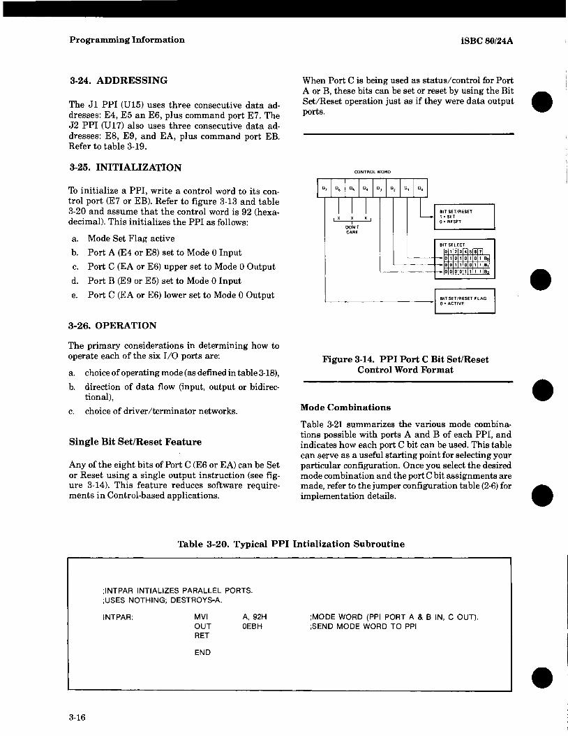
Programming Information
3-24. ADDRESSING
The J1 PPI (U15) uses three consecutive data addresses: E4, E5 an E6, plus command port E7. The J2 PPI (U17) also uses three consecutive data addresses: E8, E9, and EA, plus command port EB. Refer to table 3-19.
3-25. INITIALIZATION
To initialize a PPI, write a control word to its control port (E7 or EB). Refer to figure 3-13 and table 3-20 and assume that the control word is 92 (hexadecimal). This initializes the PPI as follows:
a. Mode Set Flag active
b. Port A (E4 or E8) set to Mode 0 Input
c. Port C (EA or E6) upper set to Mode 0 Output
d. Port B (E9 or E5) set to Mode 0 Input
e. Port C (EA or E6) lower set to Mode 0 Output
3-26. OPERATION
The primary considerations in determining how to operate each of the six lIO ports are:
a. choice of operating mode (as defined in table 3-18),
b. direction of data flow (input, output or bidirectional),
c. choice of driver/terminator networks.
Single Bit Set/Reset Feature
Any of the eight bits of Port C (E6 or EA) can be Set or Reset using a single output instruction (see figure 3-14). This feature reduces software requirements in Control-based applications.
iSBC 80/24A
When Port C is being used as status/control for Port A or B, these bits can be set or reset by using the Bit Set/Reset operation just as if they were data output ports.
CONTROL WORD
81T SET/RESET l' SET 0" RESET
L-----------~I ~I.T :g{~;SET FLAG
Figure 3-14. PPI Port C Bit Set/Reset Control Word Format
Mode Combinations
Table 3-21 summarizes the various mode combinations possible with ports A and B of each PPI, and indicates how each port C bit can be used. This table can serve as a useful starting point for selecting your particular configuration. Once you select the desired mode combination and the port C bit assignments are made, refer to the jumper configuration table (2-6) for implementation details.
Table 3-20. Typical PPI Intialization Subroutine
3-16
;INTPAR INTIALIZES PARALLEL PORTS. ;USES NOTHING; DESTROYS-A.
INTPAR: MVI OUT RET
END
A, 92H OEBH
;MODE WORD (PPI PORT A & BIN, C OUT). ;SEND MODE WORD TO PPI
•
•
•
•
•

•
•
•
•
•
iSBC80/24A Programming Information
Table 3-21. Parallel I/O Interface Configurations
PPI PPI
PPI PPI Port C PortC Configuration PortA Port B (E6 or EA) (E6 or EA)
Number (E4 or E8) (ES or E9) Lower Upper r A ....... r A ....... Co C, C2 C3 C4 Cs Cs C7
1 MODE o-IN MODE 0-1/0 -1/0- -1/0-
2 MODE o-OUT MODE 0-1/0 -1/0- -1/0-
3 MODE o-IN MODE 1-1/0 R R R I 0 0 0 U
4 MODE o-IN MODE HIO R R R 0 I I I U
5 MODE o-OUT MODE 1-1/0 R R R I 0 0 0 U
6 MODE O-OUT MODE HIO R R R 0 I I I U
7 MODE HN MODE 0-1/0 I I I R R R 0 0
8 MODE HN MODE 0-1/0 0 0 0 R R R I I
9 MODE 1-0UT MODE 0-1/0 I I I R 0 0 R R
10 MODE 1-0UT MODE 0-1/0 0 0 0 R I I R R
11 MODE 1-IN MODE HIO R R R R R R I I
12 MODE HN MODE HIO R R R R R R 0 0
13 MODE 1-0UT MODE 1-1/0 R R R R I I R R
14 MODE 1-0UT MODE HIO R R R R 0 0 R R
15 MODE 2-B MODE 0-1/0 U I I R R R R R
16 MODE 2-B MODE 0-1/0 U 0 0 R R R R R
17 MODE 2-B MODE HIO R R R R R R R R
NOTES:
I - INPUT R - RESERVED
0 - OUTPUT U - No unused driverslterminators available. These bits 1/0 - INPUT OR OUTPUT may be used, however, to connect to the serial 1/0
B - BIDIRECTIONAL interface or the Interval Timer.
3-27. 8259A PROGRAMMABLE INTERRUPT CONTROLLER (PIC) PROGRAMMING
The 8259A Programmable Interrupt Controller (PIC) is used to monitor and control all on-board and offboard interrupt requests, except the four special 8085A-2 CPU inputs. These special inputs are discussed in section 3-41.
Interrupt priority is determined by hardware jumper connection and 8259A device programming. All interrupt priority jumper connections are implemented at the interrupt jumper matrix, shown in figure 5-4, sheet 9. Possible jumper connections are listed in table 2-7. If your board is in the factory default configuration, the following jumpers are installed:
a. On-board interrupt: output 0 of the PIT is wired to IR2 on the PIC.
b. Off·board interrupt: pin P1-39 (INT2/) is wired to IR1 on the PIC.
Programming modes and initialization instructions for the 8259A device are provided in sections 3-28 through 3-37.
3-28. INTERRUPT PRIORITY MODES
The PIC has three modes for resolving the priority of interrupt inputs: (1) fully nested mode (2) rotating mode and (3) polled mode. The rotating mode has two variations: auto-rotating and specific rotating.
3-29. FULLY NESTED MODE. In this mode the PIC input signals are assigned priority from 0 through 7. The PIC operates in this mode unless specifically programmed otherwise. Interrupt IRO
,has the highest priority and IR7 has the lowest priority. When an interrupt is acknowledged, the highest priority request is available to the CPU. Lower priority interrupts are inhibited; higher priority interrupts will be able to generate an interrupt that will be acknowledged if the CPU has enabled its own interrupt input through software. An End-OfInterrupt (EO!) command is required to reset the PIC for the next interrupt.
3-30. AUTO-ROTATING MODE. In this mode the interrupt priority rotates. Once an interrupt on a given input is serviced, that interrupt assumes the
3-17

Programming Information
lowest priority. Thus, if there are a number of simultaneous interrupts, the priority will rotate among the interrupts in numerical order. For example, if interrupts IR4 and IR6 request service simultaneously, IR4 will receive the highest priority. After service, the priority level rotates so that IR4 has the lowest priority and IR5 assumes the highest priority. In the worst case, seven other interrupts are serviced before IR4 again has the highest priority. Of course, if IR4 is the only request, it is serviced promptly. In the Auto-Rotating Mode, priority shifts when the PIC chip receives an End-Of-Interrupt (EOI or AEOI) command.
3-31. SPECIFIC ROTATING MODE. In this mode the software can change interrupt priority by specifying the bottom priority, which automatically sets the highest priority. For example, if IR5 is assigned the bottom priority, IR6 assumes the highest priority. In the specific rotating mode, the priority can be rotated by writing a Specific Rotate at EO! (SEOI) command to the PIC chip. This command contains the BCD code of the interrupt being serviced; that interrupt is reset as the bottom priority. In addition, the bottom priority interrupt can be fixed at any time by writing a command word to the PIC chip.
3-32. POLLED MODE. In this mode, the 8085A-2 interrupt input is disabled. Service to the devices is achieved by programmer initiative using a Poll command. This mode is useful if there is a routine command common to several levels so that the INTA sequence is not needed.
3-33. INTERRUPT MASK
Each interrupt request input can be individually masked (disabled) by the Interrupt Mask Register UMR). The register is programmed by OCW1 (figure 3-17) Each bit in the IMR corresponds to one interrupt input. Setting the bit (bit = 1) will mask its input. The input will remain masked until its IMR register bit is reset (bit = 0). Masking one input does not affect any of the other inputs.
Note that if an interrupt is already acknowledged by the PIC (an INTAI pulse has been sent to the CPU) then the interrupting level will inhibit the lower priorities. There are two ways to avoid this condition:
a. Write an End of Interrupt (EOT) command (OCW2) to reset the ISR bit, or;
b. Set the Special Mask Mode using OCW3 (refer to section 3-34).
3-18
iSBC80/24A
3-34. SPECIAL MASK MODE
This mode is useful when some bits of the IMR are set, masking the corresponding interrupt inputs (refer to section 3-33). Since lower priority interrupts are disabled while the current interrupt is being serviced, you may wish to override this mechanism. If you want to enable lower priority interrupts when a routine is in service, you must select the Special Mask Mode (SMM). In the Special Mask Mode, the lower priority interrupts are enabled until the SMM is reset (cancelled). The higher priorities are not affected. The Special Mask Mode is selected with OCW3 (figure 3-17). For additional information on the Special Mask Mode and the operation of the Intel 8259A PIC, refer to Application Note AP-59, Using the Intel 8259A Programmable Interrupt Controller.
3-35. STATUS READ
Interrupt request inputs are handled by the following two internal PIC registers:
a. Interrupt Request Register (IRR) , which stores all interrupt levels that are requesting service.
b. In-Service Register (ISR), which stores all interrupt levels that are being serviced.
Either register can be read by writing a suitable command word and then performing a read operation.
3-36. INITIALIZATION COMMAND WORDS
The eight devices serviced by the PIC have eight addresses equally spaced in memory that can be programmed at intervals of four or eight bytes. Interrupt service routines for these eight devices thus occupy a 32- or 64-byte block, respectively, of memory. The address format for device interrupt service routine is shown in figure 3-15.
07 06 05 04 03 02 01 Do
I~I~I-I~I~I~I~I~I , I __ JI I
i r DEFINED BY AUTOMATICALLY
05-7 OF ICW1 INSERTED BY 82594
1 A1s1 A141 A131 A121 A111 A10 1 All 1 As 1 , ~
I DEFINED BY ICW2
Figure 3-15. PIC Device Interrupt Addresses
•
•
•
•
•

•
•
•
•
•
iSBC 80/24A
Bits 0-4 are automatically inserted by the PIC whereas bits 6-15 are programmed by the Initialization Command Words ICW1 and ICW2. If the address interval is eight bytes, bit 5 is automatically inserted by the PIC; if the address interval is four bytes, bit 5 is programmed in ICWl. Thus, the 32-byte or 64-byte block of addresses reserved for interrupt service routines can be located anywhere in the available memory space. Table 3-22 shows the address format inserted by the PIC for each device.
ICW1
I A7\ A6\ AS\ 1 ILTIMI ADII 1 I IC4 1
Programming Information
Initialization of the PIC consists of writing two or three 8-bit Initialization Command words as shown in figure 3-16. Since the iSBC 80/24A board does not support slave PICs, the initialization for the one PIC consists of writing two Initialization Command Words as follows:
a. The first Initialization Command Word (ICW1) consists of the following:
AO = 0
L 1 - IOW4 NEEDED o - NO ICW4 NEEDED
1 - SINGLE 0- NOT SINGLE
1 - LEVEL TRIGGERED INPUT o - EDGE TRIGGERED INPUT
ICW2
AO = 1
MOST SIGNIFICANT BITS OF VECTORING BYTE
ICW4
I 0 I 0 I o j FNM l BUF III AEOII o I AO = 1
I 1- AUTO EOI 0- NORMAL EOI
0 X - NON BUFFERED MODE 1 0 - BUFFERED MODE/SLAVE 1 1 - BUFFERED MODE/MASTER
1 - FULLY NESTED MODE o - NOT FUllY NESTED MODE
Figure 3-16. PIC Initialization Command Word Formats
3-19

Programming Information iSBC 80/24A
Table 3-22. PIC Device Address Insertion
Lower Routine Address Byte Device
Interval - 4 07 06 05 04 03 02 01
IR7 A7 A6 AS 1 1 1 0 IR6 A7 A6 AS 1 1 0 0 IRS A7 A6 AS 1 0 1 0 IR4 A7 A6 AS 1 0 0 0 IR3 A7 A6 AS 0 1 1 0 IR2 A7 A6 AS 0 1 0 0 IR1 A7 A6 AS 0 0 1 0 IRO A7 A6 AS 0 0 0 0
(1) Bits 5-7 specify the most-significant bits of the lower address byte of the interrupt service routine.
(2) Bit 3 establishes whether the interrupts are requested by a positive-true or requested by a low-to-high transition input. This applies to all input requests handled by the PIC. In other words, if bit 3 = 0, a low-to-high transition is required to request an interrupt on any of the eight levels handled by the PIC.
(3) Bit 2 specifies a 4-byte or 8-byte address interval.
(4) Bit 1 specifies whether or not there are slave (cascaded) PIC's. Since there are no slave PIC's, set bit 1 = l.
(5) Bits 0 and 4 identify the word as ICWl.
b. The second word (ICW2) specifies the upper byte (bits 8-15) of the interrupt service routine.
3-37. OPERATION COMMAND WORDS
After being initialized, the PIC can be programmed at any time for various interrupt modes. The Operation Command Word (OCW/) formats are shown in figure 3-17.
3-38. ADDRESSING
The PIC uses two consecutive addresses for writing to and reading internal registers. Address functions pertinent to programming are identified in table 3-23.
3-39. INITIALIZATION
To initialize the PIC, proceed as follows (table 3-24 provides a typical initialization subroutine):
a. Disable system interrupts by executing a DI (Disable Interrupts) instruction.
b. Write ICWI to Port DB.
3-20
J.n.I.eMlL - a DO 07 06 05 04 03 02 01 DO
0 A7 A6 1 1 1 0 0 0 0 A7 A6 1 1 0 0 0 0 0 A7 A6 1 0 1 0 0 0 0 A7 A6 1 0 0 0 0 0 0 A7 A6 0 1 1 0 0 0 0 A7 A6 0 1 0 0 0 0 0 A7 A6 0 0 1 0 0 0 0 A7 A6 0 0 0 0 0 0
c. Write ICW2 to Port D9.
. d. Write ICW4 if required by your application.
e. Enable system interrupts by executing an EI (Enable Interrupts) instruction.
NOTE Table 3-25 should be referenced when studying the programming examples. All programming procedures are PL/M calling conventions.
NOTE The PIC operates in the fully nested mode after the initialization sequence without requiring any Operation Control Word (OCW).
Table 3-23. PIC Addressing
I/O Port Data Bits Address Input Operation
(hex) 04 03
Read IRR, ISR or current 08 or OA - - interrupt level (depending
on contents of DeW3)
09 or OB - - Read Interrupt Mask Register (IMR)
Output Operation
08 or OA 0 0 Load DeW2
08 or OA 0 1 Load DeW3
08 or OA 1 X Load ICW1
09 or OB X X Load DeW1, ICW2, or ICW4, (depending on sequence)
3-40. OPERATION
After initialization, the PIC chips can be programmed at any time for the following operations:
a. Auto-rotating priority.
b. Specific rotating priority.
•
•
•
•
•

iSBC 80/24A
•
•
•
•
•
Programming Information
OCW1
OCW2 Dr De DS D. D3 D2 D1 DO
I R IsEO~ EOII 0 I 0 I L2 I L1 I La I AD = D
I ICD LEVEL TO IE RESET
OR PUT INTO LOWEST PRIORITY
0 1 2 3 • 5 I r
0 1 0 1 0 1 0 1 . 0 0 1 1 0 0 1 1
0 0 0 0 1 1 1 1
l r i.t
Non-speCific EOI ~~.J-~1.J- Specific EOL LG-L2 code of IS FF to be reset
~~+ Rotate at EOI Automatically
~14- ROlale al EOL L()-L2 code of line
14-0,g.. Sel Rolale A FF
~O~ Clear Rolale A FF
14-1,g.. Rotate priority Independently of EOI
&..1&.. No Operation
OCW3 0, 06 05 04 03 02 01 DO
I - ~SM~SM~ 0 I 1 I P IERlsl RIS I AD = D
I I I READ IN·SERVICE REGISTER
0 I 1 0 1
OON'T I I CARE
0 0 1 1
READ READ NO ACTION IR REG ISREG
WS:9tJE i8:9~~E
POLLING A HIGH ENABLES THE NEXT RD PULSE TO READ THE BCD CODE OF THE HIGH EST LEVEL REOUESTING INTERRUPT
1 SPECIAL MASK MODE
0 I 1 0 1 I
I 0 0 1 1
RESET SET NO ACTION SPECIAL SPECIAL
MASK MASK
Figure 3-17. PIC Operation Control Word Formats
Table 3-24. Typical PIC Initialization Subroutine
;'SETVEC' WILL INITIALIZE THE 8259A POINTER FOR THE INTERRUPT JUMP VECTORS WITH 8 BYTE SPACING. REG. BC CONTAINS ADDRESS OF FIRST JUMP VECTOR NOTE: IT MUST BE EVENLY DIVISIBLE BY 64 REG. A DESTROYED
SETVEC: MOV A. C ANI MASK8 ORI ICW1C OUT ICW1 MOV A. B OUT ICW2 RET
3-21

Programming Information iSBC BO/24A
c. Status read of Interrupt Request Register (IRR). d. Read mask register.
d. Status read of In-Service Register (ISR). e. Issue EOI command.
e. Interrupt mask bits set, reset, or read. Table 3-25. PIC Equates
f. Special mask mode set or reset.
PIC EQU ICW1 EQU
Table 3-26 lists details of the PIC operation. Note that ICW2 EQU
an End-Of-Interrupt (EO!) or a Special End-Of-In- OCW2 EQU terrupt (SEOI) command is required at the end of OCW3 EQU each interrupt service routine to reset the ISR. The IMR EQU EOI command is used in the fully nested and auto- ICW1A EQU rotating priority modes and the SEOI command, ICW1C EQU which specifies the bit to be reset, is used in the MASK4 EQU specific rotating priority mode. Tables 3-27 through
MASKB EQU 3-31 provide typical subroutines for the following:
RIS EQU
Read IRR. RR EQU
a. SM EQU
b. Read ISR. RSM EQU EOI EQU
c. Set mask register.
Table 3-26. PIC Operation Procedures
Operation Procedure
To set: Auto-Rotating Priority Mode In OCW2, write a Rotate Priority at EOI command (AOH) to Port DBH.
Terminate interru pt and rotate priority: In OCW2, write EOI command (20H) to DBH.
To set:
ODBH PIC + 0 PIC + 1 PIC + 0 PIC + 0 PIC + 1 16H 12H OEOH OCOH OSH OAH 6BH 4BH 20H
Specific Rotating Priority Mode In OCW2, write a Rotate Priority at SEOI command in the following format to Port DBH.
3-22
1071061051041031021011001 11 10 0 ~~
BCO OF IR LINE TO BERESET ANOIOR PUT INTO LOWEST PRIORITY
To terminate interrupt and rotate priority: In OCW2, write an SEOI command in the following format to Port DBH.
To rotate priority without EOI:
1071061051041031021011001 01100~
BCO OF ISR FLIp· FLOP TO BE RESET.
In OCW2, write a command word in the following format to Port DBH.
1071061051041031021011001 1 1 0 0 0 '?J;!...!:9
BCO OF BOTTOM PRIORITY IR LINE.
•
•
•
•
•
•
•
•
•
•
iSBC80/24A Programming Information
Table 3-26. PIC Operation Procedures (Continued)
Operation Procedure
Interrupt Request The IRR stores a "1" in the associated bit for each IR input line that is reqUiesting Register (IRR) an interrupt. To read the IRR (refer to footnote): Status
(1) Write OAH to Port 08H. (2) Read Port 08. Status format is as follows:
101~1~1~1~1~1~lool IR LINE: 7 6 S 4 3 2 1 0
In-Service The ISR stores a "1" in the associated bit for priority inputs that are being Register (ISR) serviced. The ISR is updated when an EOI command is issued. To read the ISR Status (refer to footnote):
(1) Write OBH to Port 08. (2) Read Port 08. Status format is as follows:
10710610sl04 1031021011001
IR LINE: 7 6 5 4 3 2 1 0
Be sure to reset ISR bit at end-of-interrupt when in the following modes: Auto-Rotating (both types) and Special Mask. To reset ISR in OeW2, write:
~S1041031021011001 0 1 1 0 0 L2 L1 LO -=x-
BCD iDENTIFIES BIT TO BE RESET.
Interrupt Mask To set mask bits in OeW1, write the following mask byte to Port D9H. Register
10710610sl041031021011001
IR BIT MASK: M7 M6 M5 M4 M3 M2 M1 MO 1 = MASK SET, 0 = MASK RESET
To read mask bits, read Port 09H.
Special Mask The Special Mask Mode enables desired bits that have been previously masked; Mode lower priority bits are also enabled.
To set, write 68H to 09H.
To reset, write 48H to 09H.
NOTE:
If previous operation was addressed to same register, it is not necessary to rewrite the oew.
Table 3-27. Typical PIC Interrupt Request Register Read Subroutine
;'ROIRR'
RDIRR:
READS 8259A INTERRUPT REQUEST REGISTER REG. A RETURNS RESULT
MVI OUT IN RET
A, RR OeW3 OeW3
I
3-23

Programming Information iSBC 80/24A
;'NSEOI'
NSEOI:
3-24
Table 3-28. Typical PIC In-Service Register Read Subroutine
;'RDISR' READS 8259A IN-SERVICE REGISTER REG. A RETURNS RESULT
RDISR: MVI OUT IN RET
A, RIS OCW3 OCW3
Table 3-29. Typical PIC Set Mask Register Subroutine
;'WRIMR'
WRIMR:
SETS THE 8259A INTERRUPT MASK REGISTER NOTE: A '0' WILL ENABLE THE CORRESPONDING IR LEVEL REG. C CONTAINS NEW IR MASK REG. A DESTROYED
MOV OUT RET
A, C IMR
Table 3-30. Typical PIC Mask Register Read Subroutine
;'RDIMR'
RDIMR:
READS THE 8259A INTERRUPT MASK REGISTER REG. A RETURNS RESULT
IN RET
IMR
Table 3-31. Typical PIC End Of Interrupt Command Subroutine
SENDS A NON-SPECIFIC END-OF-INTERRUPT TO THE 8259 IT CAN BE USED TO EXIT AN INTERRUPT SERVICE ROUTINE AS FOLLOWS: ISRO: ;USER SERVICE ROUTINE
MVI OUT RET
CALL NSEOI EI RET
A, EOI OCW2
•
•
•
•
•

•
•
•
•
•
iSBC80/24A
3-41. 808SA-2 INTERRUPT HANDLING
In addition to the interrupts handled by the 8259A PIC device, the 8085A-2 CPU will accept four other interrupts, without PIC intervention. In the factory default configuration, all four of these iSBC 80/24A board inputs are grounded by jumper connection at the interrupt matrix, and therefore disabled. Refer to table 2-7 and figure 5-4, sheet 9.
Both on-board and off-board sources may be used as inputs to these CPU interrupt inputs. Table 3-32 provides the priority value of each input. Vector locations are fixed within the 8085A-2 CPU for these interrupts, and cannot be altered. Priority is thus established by hardware jumper connection, as shown in jumber table 2-7. Interrupt operation of these four inputs is described in sections 3-42 thorugh 3-44.
The 8085A-2 CPU has five interrupt inputs: TRAP, RST 7.5, RST 6.5, RST 5.5, and INTR. The three restart interrupts (RST 7.5, RST 6.5, and RST 5.5) are maskable. INTR and the three restart interrupts can be enabled and disabled under software control. TRAP is non-maskable and cannot be disabled.
The RST 7.5, RST 6.5, and RST 5.5 interrupts cause the internal execution of an RST (RESTART) instruction if the interrupts are enabled and if the interrupt mask has not been set by a previously executed SIM instruction. The non-maskable TRAP interrupt causes the execution of an RST instruction independent of the state of the interrupt enable or interrupt mask. The priority and vector locations of each of the restart interrupts are given in table 3-32.
Table 3-32. Interrupt Vector Locations & Priority
Hex Interrupt Vector Priority
Location
TRAP 24 Highest
RST 7.5 3C 2nd
RST 6.5 34 3rd RST 5.5 2C 4th
INTR * 5th - 12th
* Controlled by 8259A PIC programming.
3-42. TRAP INTERRUPT
There are special considerations that must be made when the TRAP interrupt is used. The fact that the TRAP interrupt is non-maskable can present problems in at least two areas.
Programming Information
Interrupt driven systems often contain parameters that must be modified only within critical regions. A critical region can be roughly defined as a section of code that once begun must complete execution before it or another critical region that corresponds to the same system parameter(s) can be executed. A TRAP interrupt handler cannot safely alter such parameters either directly or indirectly by causing the execution of procedures or tasks that may alter such parameters.
If the hardware generates a TRAP interrupt on power up or power fail, the system must be able to process the TRAP interrupt before it is completely initialized. It should also take into account that an interrupt routine that runs with interrupts disabled can still be interrupted by a TRAP.
Because of these considerations, it is recommended that the TRAP interrupt only be used for system startup and/or catastrophic error handling such as a power failure.
It should be noted that TRAP does not destroy a previously established interrupt enable status. Executing the first RIM instruction following a TRAP interrupt yields the interrupt enable status as it was before the TRAP occurred. Following this first mandatory RIM instruction, subsequently executed RIM instructions provide current interrupt enable status.
3-43. RST 7.5, 6.5, AND 5.5 INPUTS
These interrupts can be individually masked by a SIM instruction and can thus be prevented from interrupting the processor. The priorities shown in table 3-32 do not take into account the priority of a routine that was started by a higher priority interrupt. An RST 6.5 interrupt can interrupt an RST 7.5 routine if the interrupts are re-enabled before the end of the RST 7.5 routine.
The RST 7.5 interrupt is rising-edge-sensitive and can be set by a pulse; once the request is set by a pulse, it will be remembered until the request is serviced or reset by a SIM instruction. The RST 6.5 and 5.5 interrupts are high-level-sensitive and must remain high to be recognized. Table 3-33 shows a typical restart routine.
3-44. INTR INTERRUPT
The INTR interrupt from the 8259A PIC has the lowest priority and is sampled only during the last clock cycle of a given instruction. When INTR is active, the Program Counter (PC) is pushed onto the stack and three bytes, timed by INTA/ pulses, are transferred from the PIC to the 8085A CPU.
3-25

Programming Information iSBC 80/24A
Table 3-33. Typical RST 5.5 Interrupt Routine
RST55:
ORG JMP
PUSH
EI RET
a. Byte 1 = Call instruction (OCDH).
b. Byte 2 = Lower byte of routine address.
c. Byte 3 = Upper byte of routine address.
2CH RST55
H
The 16-bit routine address must be on a 4-byte boundary or an 8-byte boundary as determined by the Initialization Command Words (ICW) previously written to the PIC. (Refer to section 3-36).
The INTR signal can be enabled or disabled by the program. It is disabled when a "RESET" occurs, and immediately after an interrupt is accepted by the 8085A-2 CPU.
3-45. RMX/80™ SOFTWARE
The iSBC 80/24A board is compatible with Intel's RMX/80 Real time Multitasking Executive. User program (tasks) can take advantage of RMX/80 to do all necessary scheduling, intertask communication, and memory space allocation. RMX/80 also provides standard I/O support software such as the Disk File handler, the Intel Analog Board handler, and the terminal handler. (Use of the RMX/80 Analog Handler may require the iSBC 80/24A board to be configured for 2.42 MHz operation.
;START ADDRESS FOR RST 5.5
! I USER ROUTINE
3-46. SYSTEM PROGRAM DEVELOPMENT
The development cycle of iSBC 80/24A board based products may be significantly reduced using the Intellec Microcomputer Development System. The resident macroassembler, text editor, and system monitor greatly simplify the design, development, and debug of the system software. Optional Diskette Operating Software for the Development System programs to be loaded, assembled, edited, and executed faster than using conventional paper tape, card, or cassette peripherals. A unique In-Circuit Emulator (ICE-85) option provides the capability to use the Development System to develop and debug software directly on your system.
Intel's high-level resident programming language, PL/M-80, provides the capability to program in a natural, algorithmic language and eliminates the need to manage register usage or allocate memory. PL/M-80 programs usually can be written in a much shorter time than assembly language programs.
* * * 3-26
•
•
•
•
•
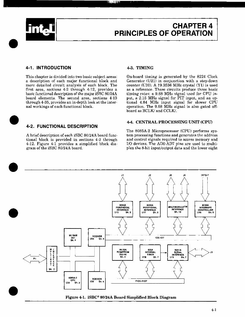
•
•
•
•
•
CHAPTER 4 PRINCIPLES OF OPERATION
4-1. INTRODUCTION
This chapter is divided into two basic subject areas: a description of each major functional block and more detailed circuit analysis of each block. The first area, sections 4-2 through 4-12, provides a basic functional description of the major iSBC 80/24A board elements. The second area, sections 4-13 through 4-35, provides an in-depth look at the internal workings of each functional block.
4-2. FUNCTIONAL DESCRIPTION
A brief description of each iSBC 80/24A board functional block is provided in sections 4-3 through 4-12. Figure 4-1 provides a simplified block diagram of the iSBC 80/24A board.
J1
8255A
4-3. TIMING
On-board timing is generated by the 8224 Clock Generator (U21) in conjunction with a step-down counter (U20). A 19.3536 MHz crystal (Y1) is used as a reference. These circuits produce three basic timing rates: a 9.68 MHz signal used for CPU input, a 2.15 MHz signal for PIT input, and an optional 4.84 MHz input signal for slower CPU operation. The 9.68 MHz signal is also gated offboard as BCLKI and CCLK/ .
4-4. CENTRAL PROCESSING UNIT (CPU)
The 8085A-2 Microprocessor (CPU) performs system processing functions and generates the address and control signals required to access memory and 1/0 devices. The ADO-AD7 pins are used to multiplex the 8-bit input/output data and the lower eight
.12 J5 J6 INTO-7
8255A 8259A PERIPHERAL PERIPHERAL MULTIMODULETM INTERRUPT INTERFACE INTERFACE INTERFACE CONTROLLER
U15 Sh.5 un Sh.6 Sh.10 U16 Sh.9
~ 8KRAM XCEIVER
U51 U35 Sh.9 100-107 Sh.4
4K-32K 8254 8251A ROM/PROM INTERVAL SERIAL J3
U52-55 TIMER INTERFACE Sh.4 U18 Sh.7 U19 Sh.7
D 80B5A-2 CPU XCEIVER
U34 Sh.3 U36 Sh.4 PIOO-PI07
Figure 4-1. iSBC® 80/24A Board Simplified Block Diagram
4-1

Principles of Operation
bits of address are strobed into Latch U64 by the Address Latch Enable (ALE) signal; the outputs of U64 are combined with the upper eight bits of the address to form the 16-bit address bus. During the remainder of the machine cycle, ADO-AD7 pins of the CPU are used for data input/output.
4-5. INTERVAL TIMER
The 8254 Programmable Interval Timer (PIT) includes three independently controlled counters which are used for on-board I/O and CPU interrupts. Each counter has its own input and output. Counter 0 is used as the CPU interrupt interval, connected to IR2 on the interrupt controller. It can also be used as an input to counter 1. Counter 1 can also be routed to the interrupt matrix or off-board via the parallel interface. Counter 2 is used exclusively for the baud rate timer, which is used to clock the serial interface.
4-6. SERIAL 1/0
The 8251A PCI provides RS232C compatibility and is configured as a data set. Synchronous or asynchronous mode, character size, parity bits, stop bits, and baud rates are all programmable. Data, clocks, and control lines to and from connector J3 are buffered with drivers and receivers.
A second serial I/O channel may be derived by jumper connection, in conjunction with port EA. (Port EA is controlled by 8255A PPI device.)
4-7. PARALLEL 1/0
The two 8255A Programmable Peripheral Interface devices provide 48 programmable I/O lines. Two bus transceivers are included to interface 16 of the I/O lines to connector Jl and J2. Four Ie sockets are provided so that, depending on the application, TTL drivers or I/O terminators may be installed to complete the interface to connectors Jl and J2. The 48 lines are grouped into six ports of eight lines each. These ports can be programmed to be simple I/O ports or strobed 110 ports with handshaking. Two ports can be programmed as bidirectional ports with control lines. The iSBC 80/24A board includes various features such as RS232C interface lines, timer gates, and interrupts that can be controlled by the parallel I/O lines.
4-8. INTERRUPT CONTROL
The interrupt section provides 12 priority interrupts. Eight interrupts connect to the inputs of the
4-2
iSBC80/24A
8259A Programmable Interrupt Controller (PIC); the remaining four interrupts connect directly to the 8085A-2 CPU. All interrupts, except TRAP, are maskable; the TRAP interrupt may be used to handle a power-fail (PFINI) signal input via auxiliary connector P2.
There are 23 jumper-selectable interrupt sources: PPI (4), PCI (3), PIT (2), external via Jl and J2 (2), Multibus lines (8), and Multimodule boards (4).
4-9. ROMIEPROM CONFIGURATION
Four sockets (U52-55) are provided for ROMI EPROM devices. The sockets are 28-pin DIP receptacles, and may be used for both 24-pin and 28-pin devices. (Refer to section 2-8 for installation instructions.) Either lK, 2K, 4K or 8K ROMIEPROM devices may be used.
In the default configuration, ROMIPROM addressing is set for 8K x 8 devices from 0-7FFFH (device types cannot be mixed). If you do not have an on-board ROMIPROM, this address space can be assigned off-board by using the PROM ENABLE signal from port E6 of the 8255A device.
The PROM enable signal enables or disables the on-board PROM. If the PROM is disabled (PROM ENABLE = 0), then all memory addresses not recognized as on-board RAM addresses are assumed to be off-board addresses. The PROM ENABLE signal originates at jumper post E32, which may be connected to an 8255A data line or a ground jumper post, or it may be left disconnected. PROM ENABLE jumpered to an 8255A output allows software control of on-board PROM access. If PROM ENABLE is connected to ground, no on-board PROM accesses are made. If PROM ENABLE is left disconnected, a 10K-ohm pull-up resistor holds PROM ENABLE = 1.
PROM Enable Example:
'Ib shadow on-board PROM over off-board memory by using bit 5 of port E6 (port C of 8255A at location U15) to control PROM ENABLE:
Install jumper: E25-E32 (Pe5-PROM ENABLE)
Design software to:
• Initialize port E6, bit 5 into the output mode
• Set port E6, bit 5 to a one to access on-board PROM
• Reset port E6, bit 5 to a zero to disable onboard PROM
•
•
•
•
•

•
•
•
•
•
iSBC 80/24A
NOTE After power-up or system reset, all the 8255A ports are in the input mode, and since the PROM ENABLE signal is pulled high by a 10K-ohm resistor, the on-board PROM is enabled.
4-10. RAM CONFIGURATION
The iSBC 80/24A board has three possible RAM configurations: 8K bytes (default configuration), 4K bytes (accomplished by disabling the lower 4k bytes of the default configuration), and 2K bytes (accomplished by disabling the lower 6K bytes of the default configuration). Addressing for the default 8K bytes configuration is set by jumpers to EOOO-FFFFH. Refer to Table 2-4 for RAM jumper connections.
In an application where the entire 64K address space must be accessed as system memory, you can disable the on-board RAM by removing all jumpers from posts E102, 103, 111, 112 and 113.
The INTROUTIBANKSEL signal can be jumpered to Multibus line ADR10/ to increase addressing capability to 128K bytes. INTROUT/BANKSEL can originate from one of several possible signals including the 8225A's port C bits and the 8085A-2's SOD signal. The INTROUT/BANKSEL line includes a 74S38 open-collector driver which either drives low or presents a high impedance.
Bank Select Example:
To address two 64K-byte banks of memory by using bit 7 of port E6 (port C ofthe 8255A at location U15) to control the Multibus line ADR10/:
Install jumpers: E16-E27 (INTROUTIBANKSEL from PC7) E206-E211 (INTROUTIBANKSEL to ADR10!)
Design software to:
• Initialize port E6, bit 7 into the output mode
• Address memory addresses OOOOOH through OFFFFH by setting port E6, bit 7 to a one, then performing a normal memory read or write using address lines ADRO-ADRF
• Address memory addresses 10000H through 1FFFFH by resetting port E6, bit 7 to a zero, then performing a normal memory read or write using address lines ADRO-ADRF
Principles of Operation
NOTE The iSBC 80/24A's on-board RAM and PROM (if enabled) are addresses in both banks. To use the bank select feature in a multimaster configuration, be sure to lock the Multibus whenever ADR10/ is driven.
4-11. MULTIMODULETM BOARDS
Optional Multimodule boards are interfaced to the iSBC 80/24A board via iSBX bus eonnectors J5 and J6. If present, the Multimodule board at J6 will utilize addresses FO-FF. Likewise, if present, the J5 Multimodule board will utilize addresses CO-CF. If neither of the boards are present, these addresses may be used for other applications.
4-12. MULTIBUSTM INTERFACE CONTROL
The Multibus interface includes an Intel Bus Controller, bidirectional address an data bus drivers, and the bus interrupt driver/receivers. The bus controller allows the iSBC 80/24A board to operate as a bus master in a serial or parallel priority arrangement with other bus masters in the system in which the 8085A-2 CPU can request the Multibus lines only when needed.
4-13. CIRCUIT ANALYSIS
The schematic diagram for the iSBC 80/24A board is provided in figure 5-4, sheets 1 through 10. Signals which traverse from one sheet to another are identified with an alpha character(s) in a box (e.g., @] or ~). Each boxed characterCs) will represent the same signal throughout figure 5-4. To follow a particular signal from one sheet to another, merely turn to the sheet indicated next to the signal name. After you turn to the indicated sheet, look for the signal's boxed character. Signals which enter or exit the board do not have boxed characters.
Both active-low and active-high signals are used on the iSBC 80l24A board. A signal which ends with a slash (e.g., READ!) is active-low, meaning it will be true at ~ 0.4 volts. Conversely, a signal without the slash (e.g., ALE) is active-high, meaning it will be true at ?: 2.4 volts.
The following sections make reference to the signals in figure 5-4.
4-3

Principles of Operation
4-14. INITIALIZATION
When power is applied in a start-up sequence, the contents of the 8085A-2 CPU program counter, instruction register, and interrupt enable flip-flop are subject to random factors and cannot be predicted. For this reason, a power-up sequence is used to set the CPU, bus controller, and 110 ports to a known internal state.
The 8224 clock generator produces the RESET signal at power-up time (figure 5-4, sheet 3). This signal is routed to the CPU ad throughout the board. If power is already on, the RESET signal may be generated by the AUX RESET/signal (front panel switch closure). The RESET signal is routed offboard via Pl-14, as INIT/. Notice that INITI may also be an input from Pl-14.
The RESET signal clears the CPU program counter, instruction register, and interrupt enable flip-flop; sets the parallel 110 ports to the input mode; resets the serial 1/0 port to the "idle" mode; resets the bus controller; and, via the INIT/signal sets the system to a known internal state.
4-15. CLOCK CIRCUITS
The 8224 Clock Generator (U21) OSC output is divide-by-2 (at U20) to produce the 9.68 MHz reference signal (figure 5-4, sheet 3). A divide-by-4 signal (4.84 MHz) is available by jumper connection. The reference signal is routed to three areas:
a. 8085A-2 CPU (sheet 3)
b. iSBX Bus connectors J5 and J6 (sheet 10)
c. BCLK/and CCLKI gates (sheet 2)
The 2.15 MHz 02TTL signal, produced by the 8224 Clock Generator, is used as a reference for the 8254 PIT (sheet 7). This 2.15 MHz signal is reduced to 1.075 MHz by counter U20, and serves as the CKLO, CLK1 and CLK2 inputs for the PIT.
4-16. 8085A-2 CPU TIMING
The 8085A-2 CPU internally divides the 9.68 or 4.84 MHz clock input by two to develop the timing requirements for the various time-dependent functions. These functions are described in the following paragraphs.
4-4
iSBC 80/24A
4-17. INSTRUCTION TIMING
The execution of any program consists of read and write operations, where each operation transfers one byte of data between the CPU and memory or between the CPU and an I/O device.
An instruction cycle is the time required to fetch and execute an instruction. During the fetch phase, the selected instruction (consisting of up to three bytes) is read from memory and stored in the operating registers ofthe CPU. During the execution phase, the instruction is decoded by the CPU and translated into specific processing activities.
Each instruction cycle consists of up to five machine cycles. A 'machine cycle' is required each time the CPU accesses memory or an I/O device. The fetch phase requires one machine cycle for each byte to be fetched. Some instructions do not require any machine cycles other than those necessary to fetch the instructions from memory; other instructions, however, require an additional machine cycle(s) to write or read data to or from memory or I/O devices.
Every instruction cycle has at least one reference to memory during which time the instruction is fetched. An instruction cycle must always have a fetch, even if the execution ofthat instruction requires no reference to memory. The first machine cycle in every instruction cycle is therefore a fetch, and beyond that there are no specific rules. For instance, the IN (input) and OUT (output) instructions each require three machine cycles: fetch (to 0 btain the instruction), memory read (to obtain the I/O address of the device), and an input or output machine cycle (to complete the transfer).
Each machine cycle consists of a minimum of three and a maximum of six states (excluding any WAIT states) designated TJ through T6. A 'state' is the smallest unit of processing activity and is defined as the interval between two successive falling edges of the CPU clock. Each state (or CPU clock cycle) has a duration of 206 nanoseconds (assuming 9.68 MHz input clock).
•
•
•
•
•

•
•
•
•
•
iSBC 80/24A
Every machine cycle normally consists of three T-states with the exception of an opcode fetch, which consists of either four or six T-states (plus WAIT states). The actual number of states required to execute any instruction depends on the instruction being executed, the particular machine cycle within the instruction cycle, and the number of 'wait' states inserted into the machine cycle. The wait state is generated by circuitry external to the CPU.
At the 4.84 MHz operating speed there are no wait states imposed when the CPU is addressing on· board RAM. There will be wait states imposed, however, in the following operations (at 4.84 MHz):
a. When addressing on-board ROM/EPROM with access time greater than 300 ns;
b. For interrupt acknowledge cycles; or
c. When addressing off-board RAM, PROM, or I/O devices via the Multibus lines, or iSBX Bus.
At the 2.42 MHz operating speed, no wait states are required for anyon-board requests but are required for iSBX Multimodule operation, and other offboard requests. Figure 4-2 is presented to show the relationship between an instruction cycle, machine cycle, and T-state. This example shows the execution of a Store Accumulator Direct (STA) instruction involving on-board memory. Notice that for this instruction the opcode fetch (machine cycle M1)
requires four T-states and the remaining three cycles each require three T-states.
The opcode fetch is the only machine cycle that requires more than three T-states. This is because the CPU must interpret the requirements of the opcode fetched during TI through T3 before it can decide what must be done in the remaining T-state(s).
There are seven types of machine cycles, each of which can be differentiated by the states of three CPU status lines (1O/M, SO, and Sl) and three CPU
Principles of Operation
control lines (RD, WR, and INTA). Table 4-1 lists the states ofthe CPU status and control lines during each of the seven machine cycles and during a CPU halt.
Table 4-1. CPU Status & Control Lines
Status Control
Machine Cycle 101M RD WR INTA so S1
Opcode Fetch 0 1 1 0 1 1 Memory Read 0 0 1 0 1 1 Memory Write 0 1 0 1 0 1 1/0 Read 1 0 1 0 1 1 1/0 Write 1 1 0 1 0 1 INTR Acknowledge 1 1 1 1 1 0 Bus Idle X X X 1 1 1 Halt T8 0 0 T8 T8 1
0= Logic "0" T8 = High Impedance 1=Logic"1" X = Unspecified
4-18. OPCODE FETCH TIMING. Figure 4-3 shows the timing relationship of a typical opcode fetch machine cycle. At the beginning ofTI of every machine cycle, the CPU performs the following:
a. Pulls IO/M low to signify that the machine cycle is a memory reference operation.
b. Drives status lines SO and Sl high to identify the machine cycle as an opcode fetch.
c. Places high-order bits (PCH) of program counter onto address lines A8-A15. These address bits will remain true until at least T 4.
d. Places low-order bits (PCL) of program counter onto address/data lines ADO-AD7. These address bits will remain true for only one clock cycle, after which ADO-AD7 go to their high-impedance state as indicated by the dashed line in figure 4-3.
e. Activates the Address Latch Enable (ALE) signal.
1--------------- INSTRUCTION CYClE----------------.j
MACH~NE
CYCLE
T STATE
ClK
TYPE OF MACHINE CYCLE
ADDRESS BUS
DATA BUS
MEMORY READ MEMORY READ MEMORY REAO MEMORY WRITE
THE ADDRESS ICONTENTS OF THE THE ADDRESS IPC+ 1) POINT THE ADDRESS IPC + 21 POINTS THE ADDRESS IS THE DIRECT PROGRAM COUNTER) POINTS TO THE 0 THE SECOND BYTE OF TO THE THIRD BYTE OF THE ADDRESS ACCESSED IN MZ ~~~~~~;~~~OPCODEI OF THE THE INSTRUCTION INSTRUCTION AND M3
lOW ORDER BYTE OF THE HIGH ORDER BYTE OF THE CONTENTS OF THE INSTRUCTION OPCOOE ISTA) DIRECT ADDRESS DIRECT ADDRESS ACCUMULATOR
Figure 4-2. Typical CPU Instruction Cycle
4-5

Principles of Operation iSBC 80/24A
/\t the beginning of T2, the CPU pulls the RDI line low to enable the addressed memory device. The device will then drive the ADO-AD7 lines. After a period oftime, as determined by the access time of the addressed memory device, valid data (the DCX instruction in this example) will be present on the DO-D7 lines. During T3 the CPU loads the data on the DO-D7 lines into its instruction register and drives RDI high, disabling the addressed memory device. During T 4 the CPU decodes the opcode and decides whether or not to enter T5 on the next clock cycle or start a new machine cycle and enter Ts and then T6 before beginning a new machine cycle.
Figure 4-4 is identical to figure 4-3 with one exception, which is the use of the READY input to the CPU. As shown in figure 4-4 the CPU examines the state of the • READY input during T2. If the READY input is high, the CPU will proceed to T3 as shown in figure 4-3. If the READY input is low, however, the CPU will enter the Twait state and stay there until READY goes high. When READY goes high, the CPU will exit the T wait state and enter T3. The external effect of using the READY input is to preserve the exact state of the CPU signals at the end ofT3 for an integral number of clock periods before finishing the machine cycle. This 'stretching' of the system timing, in effect,
M, 'OF) M,
SIGNAL T, T2 T3 T. Ts TS T,
10-L.I L.I LJ LJ LJ L1 \....J ClK • r--:x x:::: 101M, 101M ~ 0, s, • " SO : ,
S1.S0 ~
I--:x y--Aa-A,5 PCH UNSPECIFIED - -OUT IN - :x ADo·ADJ pel }--{ DO,D7 'DCXI ... ------ ------ ------~ - I -ALE r-\ f\... -
AD • Figure 4-3. Opcode Fetch Machine Cycle
M, 'OF)
SIGNAL T, T2 TWAIT T3 T. TS T6
10-Lt '-' Lt l.J l.J l.J ~ ClK • 101M, - [X 101M'" 0,51'" 1, SO"' 1 51, SO -
- tx AS-A,5 PCH UNSPECI F I ED ,..... - ~
OUT IN
ADo·AD7 PCl ~-( DO,D 7 ,DCX) >.---------- - ---- ! ALE ~ - 1
AD /'J
READY ~ "' 'C I-
Figure 4-4. Opcode Fetch Machine Cycle With Wait State • 4-6

•
•
•
•
•
iSBC 80/24A
increases the allowable access time for memory or I/O devices. By inserting T wait states, the CPU can accommodate slower memory or slower I/O devices. It should be noted, however, that access to the onboard ROM/PROM and I/O ports usually imposes a T wait state only when operating at 4.84 MHz. T wait states are always imposed when accessing system memory or I/O devices via the Multibus lines.
4-19. MEMORY READ TIMING. Figure 4-5 shows the timing of two successive memory read machine cycles, the first without a T wait state and the second with one T wait state. Disregarding the states of the SO and Sl lines, the timing during TJ through T3 is identical with the opcode fetch machine cycle shown in figure 4-3. The major difference between the opcode fetch and memory read cycles is that an opcode fetch machine cycle requires four or six T-states whereas the memory read machine cycle requires only three T-states. One minor difference between the two cycles is that the memory address used for the opcode fetch cycle is always the contents of the program counter (PC), which points to the current instruction; the address used for a memory read cycle can be one of several origins. Also, the data read from memory is placed into the appropriate register instead of the instruction register. Note that T wait state is not imposed during a read of on-board ROM/PROM.
MR OR lOR SIGNAL
Tl T2 T3
I-Lr-Lr-~ elK
101M, 10-tx 101M· 0 (MRI OR 1 IIORI. 51 = 1. so· a 51.50 10-
- tx A8'A15 - OUT IN -~ AO-A7 1>< 00.07 )-AOo·A07 - t ) ALE I{\ - 1.. iiD \ I
REAOY "-
Principles of Operation
4-20. 1/0 READ TIMING. Figure 4-5 also illustrates the timing of two successive I/O read machine cycles, the first without a T wait state and the second with one Twait state. With the exception ofthe 101M status signal, the timing of a memory read cycle and an I/O read cycle is identical. For an I/O read, 101M is driven high to identify that the current machine cycle is referencing an I/O port. One other minor exception is that the address used for an I/O read cycle is derived from the second byte of an IN instruction; this address is duplicated onto both the A8-A15 and ADO-AD7 lines. The data read from the I/O port is always placed in the accumulator specified by the IN instruction. Note that in the 2.42 MHz mode a T wait is not imposed during the access of on-board I/O devices; Twait states are imposed during the access of system I/O devices via the Multibus lines.
4-21. MEMORY WRITE TIMING. Figure 4-6 shows the timing of two successive memory write machine cycles, the first without a T wait state. Again, disregarding the states of the SO and Sl lines, the timing during TJ is identical to the timing of an opcode fetch, memory read, and I/O read cycles. The difference occurs, however, at the end of TJ. For instance, in a memory read cycle the ADO-AD7Iines are disabled (high impedance) at the beginning ofT2 in anticipation of the returned data. In a memory write cycle, the ADO-AD7 lines are not disabled and
MR OR lOR
Tl T2 TWAIT T3
'--' \........I Lr-'--' \. 101M "'0 (MRI OR 1 (lORI. Sl:. 1,sa "'0 )
) OUT IN
> ~ 1-< Ao-A 7 DO·D 7
r\ V-\l f- I-
~
L--r--~ ~ ~ ....--
•
Figure 4-5. Memory or 1/0 Read Machine Cycle
4-7

Principles of Operation iSBC80/24A
----MWOR lOW MWOR lOW
SIGNAL T1 T2 T3 T1 T2 TWAIT T3
r-~ ~ ~ ~ ~ ~ W-I\. elK
r-D< 101M, 101M. 0 IMWI OR 1 IIOWI, 51' 0, SO, 1 :X 101M' 0 IMWI OR 1 ,'OWI,51 • 0, so • 1 )
S1,SO ~
r-
D< AB'A 15 ) r-
OUT OUT OUT OUT r-b< 0 0 ,07 ) ADo·AD7 AO·A7 0 0 .0 7 AO·A7 -
ALE h r-\ lr r-
r I-WA / \
READY L-~ "-
~ 0 ..
Figure 4-6. Memory or I/O Write Machine Cycle
the data to be written into memory is placed on these lines at the beginning ofT2. The Write (WR/) line is driven low at this time to enable the addressed memory device. During T2 the READY input is checked to determine if a Twait state is required. If the READY input is low, Twait states are inserted until READY goes high. During T3, the WRI line is driven high to disable the addressed memory device and terminate the memory write operation. Note that the contents on the address and data lines do not change until the next Tl state.
4-22. I/O WRITE TIMING. Figure 4-6 also illustrates the timing of two successive I/O write machine cycles, the first without a Twait state and the second with one Twait state. With the exception of the 101M status signal, the timing of a memory write cycle and an I/O cycle are identical.
4-23. INTERRUPT ACKNOWLEDGE TIMING. Figure 4-7 shows the CPU timing in response to the INTR input being driven high by PIC U17 (assuming the CPU interrupt enable flip-flop has been set by a previously executed Enable Interrupt instruction). The status of the TRAP, RST 7.5, RST 6.5, RST 5.5, and INTR inputs are sampled during CLK of the T-state immediately preceding Tl ofMl. IflNTR was the only valid interrupt, the CPU clears its interrupt enable flip-flop and enters the Interrupt Acknowledge (INA) machine cycle. With two exceptions, the INA machine cycle is identical with the Opcode Fetch (OF) machine cycle. The first exception is that 101M = 1, which signifies that the opcode fetched will be
4-8
from an 110 device. The second exception is that INTA is asserted instead of RD. Although the contents of CPU program counter are sent out on the address lines, the address lines are ignored.
When INTA is asserted, the PIC provides a CALL instruction which causes the CPU to push the contents of the program counter onto the stack before jumping to a new location. After receiving the CALL opcode, the CPU performs a second INA machine cycle (M2) to access the second byte of the CALL instruction from the PIC. The timing ofM2 is identical with Ml except that M2 has three T-states. M2 is followed by M3 to access the third byte of the CALL instruction. When all three bytes have been received, the CPU executes the instruction. The CPU inhibits the incrementing of the program counter during the three INA cycles so that the correct program counter value can be pushed onto the stack during M4 and Ms.
During M4 and Ms, the CPU performs Memory Write (MW) machine cycles to write (push) the contents of the program counter onto the top of the stack. The CPU then places the two bytes access during M2 and M3 into the upper and lower bytes of the program counter. This has the same effect as jumping the execution of the program to the location specified by the CALL instruction.
After the interrupt service routine is executed, the CPU pops the stack and loads it into the program counter, and resumes system operation at the point of the interrupt. (It is the programmer's responsibility to ensure that the interrupt enable flip-flop is set before returning from the service routine.)
•
•
•
•
•
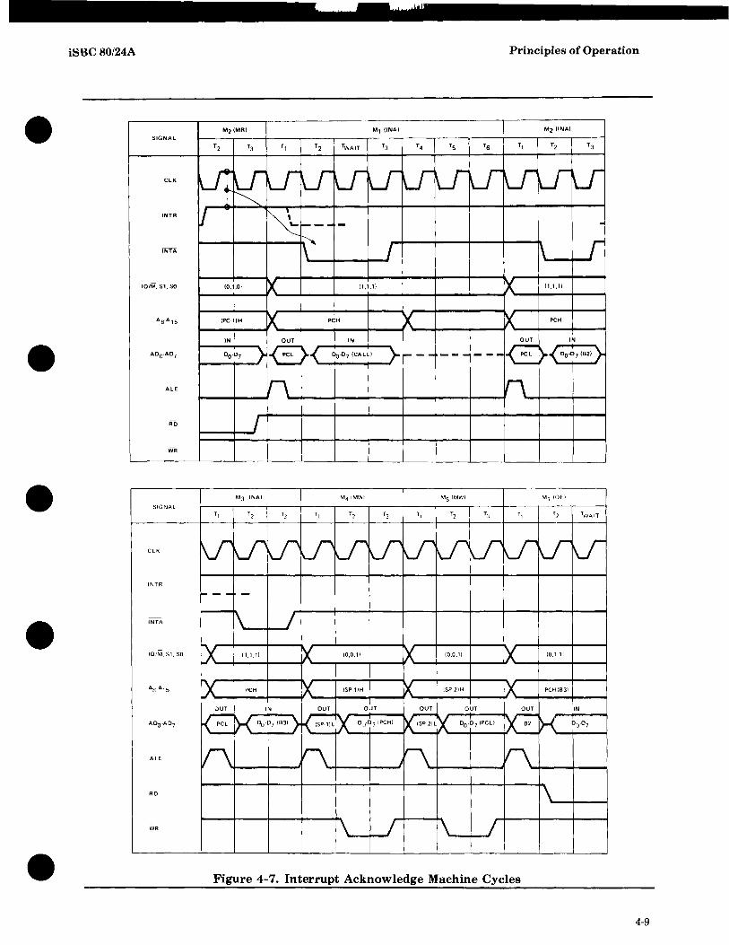
iSBC 80/24A Principles of Operation
• M21MRI M,IINAI M21lNAI SIGNAL
T 2 T3 T, T2 TWAIT T3 T4 TS T6 T, T2 T3
ClK U. V Lr U-lJ Lr U-Lr u Lr u u-INTR V ~ --- - -
K' J INTA I 1\
101M, $1, SO (0,1,0) ~ 1'.'.11 lX. (1,1,1)
AS-A15 IPC·lIH D< PCH D< D< PCH
• IN
I€ IN OUT IN
ADo·ADJ 00 .07 } ~ 00 .07 (CALL) } I- -- --- - --IE ~< 00 .0 7 IB21}
ALE n h RD I -WR
• M3 (INA) M4 (MWI MSIMWI M, (OFl
SIGNAL
T, T2 T3 T, T2 T3 T, 12 T3 T, T2 TWAIT
ClK V lr V lJ lr V V V V V V V INTR
~-- -
• - \ INTA
tx IOiM, 51, so (1,1,1) D( 10,0,11 D( (0,0,11 X (0,1,1)
Aa'A15 tx PCH !X (SP·,)H ~ (SP·2)H X PCH(B3)
OUT IN OUT OUT OUT OUT OUT IN
ADO·AD7 ~ KDo 7 (83) } ~ 0 0.0 7 (PCH) ~ DO -D 7 (pel! x:= K 0 0 '°7
ALE f\ n r\ r\ --RD
-WR
I
• Figure 4-7. Interrupt Acknowledge Machine Cycles
4-9

Principles of Operation
4-24. ADDRESS BUS
The lower eight bits (ADO-AD7) of the memory address or 110 address (depending on whether a memory reference machine cycle or an 110 reference machine cycle is in progress) are output by the CPU during the first clock cycle (T1). The CPU ADO-AD7 pins become the source to or input from the data bus during the second and third cycles (T2 and Ta). The trailing edge of the Address Latch Enable (ALE) signal issued by the CPU during Tl strobes these eight address bits into Latch U64 (sheet 3). The lower eight address bits (AO-A 7) from U64 are placed on the address bus together with the highorder address bits (A8-AF). These address bits are routed throughout the board and off-board via the Multibus address drivers (U60, 61, sheet 2).
Address bits AA through AF are routed to the Decode PROM (U32) on sheet 8. This PROM is a factory programmed deice designed to generate most of the key 110 signals used on the board. Decode PROM operation is described in section 4-30, "Board I/O Operation". Appendix B provides a Decode PROM map and structure description.
4-25. BUS TIME-OUT
Bus Time-Out one-shot U39-12 (sheet 3) is retriggered by the leading edge of the ALE signal, which is asserted by the CPU during Tl of every machine cycle. If the CPU is halted, or if the CPU is in a wait-state for approximately 10 milliseconds, U39 times out and asserts the BTMO signal on pin 34 of the auxiliary but (P2). If jumper E97-106 is installed, the BUS TIME OUT/ signal (U39-5) drives the CPU READY line high through U31 and allows the CPU to exit the wait state.
4-26. DATA BUS
The CPU ADO-AD7 pins become the source or destination of the data but DBO-DB7 during T2 and Ta clock cycles. Data can be sourced to or input from the following:
a. Data LatchlDriver U62 (sheet 2).
b. Data Bus Transceiver U36 (sheet 4).
c. RAM device U51 (sheet 4).
d. Data LatchlDriver U35 (sheet 9).
LatchlDriver U35 (sheet 9) also serves as the data bus latch/drive for each PPI device (U15, U17) and the Multimodule board devices (sheet 10). Bus Transceiver U36 serves as the data bus receiver/ driver for the PIC (U19) and the PIT (U18).
4-10
iSBC80/24A
4-27. READIWRITE SIGNAL GENERATION
The COMMAND/ signal, which is used in conjunction with the various on-board read/write operations, is generated when the CPU RD/ or WRI signal is true. The following paragraphs describe how the various 110 and memory control signals are generated.
4-28. I/O CONTROL SIGNALS
The 110 control signals are derived simply by gating the status of the CPU IOIM, RDf, and WRI pins. For example, the 10/ signal is the buffered 101M pins status; the 110 WRT/ signal is the logical AND of the IOf and WR/ pin status.
4-29. MEMORY CONTROL SIGNALS
The MRDf and MWRT/ signals (sheet 3) are also ~rived simply by gating the status of the CPU IOIM, RDf, and WRf pins. For example, the MWRTf signal is the logical AND of the WR/ and inverted IOIM pin status.
The CPU signals RD and WR are routed to the RAM (sheet 4) as 85RDf and 85WRTf. These signals are used by the RAM device to indicate Read or Write mode.
The Bus Controller (U57, sheet 2) uses the MRD/ and MWRTf signals to control off-board memory transactions.
The signal READ/ is used to gate the U63 receiver device (sheet 2). This device is used for all off-board memory read transactions.
The CPU signal Sl (sheet 3) is used to establish the mode of the U36 bus transceiver. All on-board PROM data is routed through this device during the read cycle.
If no on-board RAM address is decoded by the 74LS138 (U28, sheet 4), the RAMACKI is false and the bus controller will assume an off-board read/ write request has been made. The off-board request will be acknowledged by XACKI(Pl-23, sheet 2) which subsequently produces the MULTIBUS RDY/ signal. This in turn, provides the CPU ready signal.
For an on-board ROM/EPROM read, address bits AO-AF are routed to PROM jumper matrix E177-E197 and the ROM/EPROM devices. bits AO-A9 are used for addressing 4K and smaller devices; bits
•
•
•
•
•

•
•
•
•
•
iSBC 80/24A
AO-A9 and AC are used for 8K devices. The signals PrYPEO and PrYPE1 indicate the amount of onboard PROM. The following must be true for an onboard PROM read to occur:
a. Address must be recognized by Decode PROM U32 (sheet 8) to produce either DCDPROM11 or DCDPROM2/.
b. The CPU 101M signal must be false (101 = 1).
c. PROMACKI must be true.
d. PROM ENABLE must be true.
When these conditions occur, PROMACKI will disable the RAM chip select decoder. The DCDPROM signals will decode one-of-four on-board ROM chip selects to enable one of the ROM/EPROM devices. This decoder (U49, sheet 4) is gated by PROMACKI and 85RDI.
If the ROM read is an off-board request, there will be no on-board acknowledge signal and wait states will be inserted by U31 (sheet 3) until XACK is received to produce MULTIBUS RDYI (sheet 2). Wait states will be inserted for 10ms maximum (refer to section 4-35).
4-30. 1/0 OPERATION
The iSBC 80/24A board must distinguish between on-board and off-board I/O operations. The Decode PROM (U32, sheet 8) examines address bits AA-AF to determine if the current address is valid. Several other qualifiers are used by the Decode PROM to establish whether the address is on or off-board. The signal 10/ must be true to indicate an I/O request rather than memory. The signal MMPRESENTI will be true if one or both iSBX Bus connectors (sheet 10) have board installed.
4-31. ON-BOARD 110 OPERATION
If the address is determined to be an on-board location, the signal ONBDIO (sheet 8) will be true (ONBDIO = 1). This signal is routed to the bus controller, preventing a bus cycle and to the Multibus data receivers (U63, sheet 2), turning them off. At the same time, the Decode PROM will enable one of the I/O chip select signals, via decoder U48 (sheet 8).
Each of these I/O chip select signals indicates its destination (e.g., 59CSI enables the 8259A PIC). Port addresses are also shown.
Principles of Operation
Multimodule chip select signals (MMCSOIMMCS3/) are selected by further decoding address bits AB and AC. This decoder (U4H, sheet 8) is gated by bit 3 of the U48 chip select decoder.
Two signals can be used to furnish the required CPU READY signal. At 4.84 MHz operation, if the addressed, on-board I/O device is not a Multimodule board, the signal IOSYNCI (sheet 8) will furnish the READY signal, via the wait-state circuitry (sheet 3). If the CPU is operating at the slower speed (2.42 MHz), IOSYNCI will provide a READY signal without a wait state, via jumper E96-105 (sheet 3).
If the addressed, on-board I/O device is on a Multimodule board, the signal IOASYNCI will supply the required READY signal (via wait-state circuitry). A minimum of one wait-state is required when accessing a Multimodule board.
4-32. OFF-BOARD 1/0 OPERATION
An off-board I/O operation is characterized by the signal ONBDIO being false (ONBDIO = 0), and the absence of anyon-board acknowledge (ACK, sheet 3) signal. These two conditions will allow the bus controller (U57, sheet 2) to institute a bus cycle, provided the command signal (CMD, sheet 2) is true. At the same time, the Mult:lbus data receivers (U63, sheet 2) will be turned·on. If an XACKI signal is not received within 10 ms of command time, the failsafe timer will produce the required READY signal (U39, sheet 3).
4-33. MULTIBUS® INTERFACE
The Multibus Interface allows the iSBC 80/24A board to use a common system bus with other master devices, thus sharing memory and I/O resources. The Multibus Interface (sheet 2) consists of a 3218 bus controller (U57), a data latch/driver (U62), a data receiver (U63), and address drivers (U60, 61).
The bus controller arbitrates all iSBC 80/24A board requests for use of the Multibus lines, synchronously with respect to the Bus Clock (BCLK/). When the iSBC 80/24A board acquires control of the bus, the bus controller generates the appropriate memory or I/O command signal, gates data on! off the bus, at the appropriate times. An external RC network connected the bus controller's DelayAdjust (DLYADJ/) input guarantees the required setup and hold time relationship between the address/data lines and the control signals.
4·11

Principles of Operation
The negative-going edge of the Bus Clock (BCLKI) signal provides a timing reference for the controller's bus arbitration logic.
Bus arbitration activity begins when an off-board memory or an I/O request is generated and applied to the Bus Request (BCRl) and Transfer Start Request (XSTR) inputs. The request is strobed in by RSTBI (which is always enabled). Following the next rising and falling edge of BLCKI the bus controller generates Bus Request, BREQI (connector pin PI-I8) and forces Bus Priority Out, BPROI (connector pin PI-I6) inactive (high). BREQI is used to request the system bus when priority is decided by a parallel priority resolution circuit (section 2-21). BPROI is used to allow lower priority masters to gain control of the bus when a serial priority resolution structure is used (section 2-20). BPROI would go to the Bus Priority In (BPRNI) input of the next lower priority master.
When an off-board request activates the Transfer Start Request input (XSTR) and ADEN/ is activated, the bus controller's timing logic starts the internal sequence which ultimately (depending on the RC network at DLYADJI) generates the appropriate memory/IO read/write control output (MRDC/, MWTC/, IORC/, or IOWCI) based on the active command request input (MRD/, MWRT/, IORDI or IOWRTI) from the CPU.
When control of the bus is granted to the iSBC 80/24A board, a low level appears on its Bus Priority In (BPRNI) input. The bus controller activates its BUSY/ (connector pin PI-I7) and Address and Data Enable (ADENI) outputs. BUSY/ "locks" the iSBC 80/24A board onto the bus by prohibiting any other master from acquiring control of the bus. ADEN/ enables the system address drivers (U60, 61) and data latch/drivers (U62). When the external acknowledge signal (XACK/ or AACKI) is received it will be grated (as MULTIBUS RDYI) the CPU RDY input via the wait circuity (sheet 3).
The iSBC 80/24A board can only lose control of the Multibus lines if its BPRNI input goes high or the bus request inputs (ACK • ONBDIO • CMD) go inactive causing the Transfer Complete input (XCPI) to be activated. In either case, the iSBC 80/24A board will only lose the buse if it is not in the middle of a transfer and its override flip-flop is not set (see section 4-34).
A low level on the bus controller's INIT/ input will initialize (reset) the device.
4-12
iSBC 80/24A
4-34. MULTIBUS® OVERRIDE FEATURE
Ifit is necessary to guarantee that the iSBC 80/24A board not lose control of the Multibus lines, the override function can be invoked by executing an OUTPUT instruction to port D5 (hexadecimal). If data bit 0 is a "1" when this output instruction is executed, the Override flip-flop (U31, sheet 2) is set. While this flip-flop is set, the board cannot relinquish control of the Multibus lines. If data bit 0 is "0" when the output instruction to port D5 is executed, or if the Reset signal (RSTI) is activated, the Override flip-flop is reset. The iSBC 08/24A board must clear the Override capability when it is finished with exclusive use of the Multibus lines.
4-35. FAILSAFE TIMER
If the CPU tries to access a memory or I/O device but that device, for whatever reason, does not return an acknowledgment (READY) indication, the 8085A-2 remains in a WAIT state until READY is received. The failsafe timer is designed to prevent holding the system in the WAIT condition. A 74LS123 one-shot device (U39, sheet 3) is triggered by ALE at the beginning of each machine cycle. If the one-shot is not re-triggered (Le., if another cycle does not begin) with approximately 10 ms, the 74LS123 times-out and its output is gated through to the RDY pin on the 8085A-2, thus ending the WAIT state. The iSBC 80/24A board is shipped with the failsafe timer enabled. To disable the timer, remove jumper E97-106.
4-36. INTERRUPT OPERATION
Interrupt circuity is shown on sheet 9. The major components include the jumper matrix, the 8259A PIC, and the 8286 Bus Transceiver.
The jumper matrix is shown in its factory configuration. External interrupt requests (lNTOI-INT7 I, INTR/, PFINI) enter the board via connectors PI and P2. These interrupts may be assigned priority by jumper connection to the appropriate posts. Similarly, internal interrupt requests may be jumper connected to establish priority. Internal requests include:
OITO OITI RxR TxR TxE
Timer 0 Timer 1 Receiver Ready Transmitter Ready Transmitter Empty
•
•
•
•
•

•
•
•
•
•
iSBC 80/24A
MIOINTO -MIOINT1 -MIOINT2 -MIOINT3 -
PIAl! pm1 PIA2 pm2
! Multimodule Board Interrupts
Parallel Port Interrupts
Jumper connections are shown in table 2-7.
In addition to the interrupt requests which are handled by the 8259A PIC, four lines are direct inputs to the 8085A-2 restart functions. These functions are described in section 3-37.
The iSBC 80/24A board can generate external interrupts (via Pl-28) by jumpering the INTROUT/ BANKSEL signal to any of the Multibus interrupt lines (INTO-INT7). INTROUTIBANKSEL can originate from one of several possible signals including the 8255A's port C bits and the 8085A-2's SOD signal. The INTROUTIBANKSEL line includes a 74S38 open-collector driver which either drives low or presents a high impedance.
Interrupt Out Example:
To generate an off-board interrupt by using bit 6 of port E6 (port C of the 8255A - location U15) to control the Multibus signal INT6/:
Install jumpers: E16-E26 (lNTROUTIBANKSEL from PC6) E206-E212 (INTROUTIBANKSEL to INT6)
Principles of Operation
Design software to:
• Initialize port E6, bit 6 to the output mode
• Set port E6, bit 6 to a one
• Generate an interrupt by resetting port E6, bit 6 to a zero, then setting port E6, bit 6 to a one
NOTE This method produces an interrupt pulse approximately 1 microsecond in duration on the Multibus INT6/ line.
Port addressing and operation of the 8259A PIC are described in sections 3-27 through 3-36.
4-37. CONCLUSION
This chapter presents a basic description of each major iSBC 80/24A board functional block, as shown in figure 4-1. The Preface of this manual (page iii) provides a list of additional Intel publications with information on related topics.
* * * 4-13

•
•
•
•
•

•
•
•
•
•
CHAPTERS SERVICE AND REPAIR INFORMATION
5.1 INTRODUCTION
This chapter provides service and repair information, component layout, jumper location, and schematic diagrams for the iSBC 80/24A Single Board Computer.
5.2 SERVICE AND REPAIR ASSISTANCE
Customer Support Service Engineering provides two separate services for product replacement and repair: a Return Replacement Authorization (RRA) for direct replacement, and a Direct Return Authorization (DRA) for repair.
The RRA service replaces a defective product. Return the defective product to Intel, freight prepaid. Intel will replace the product (bearing a new serial number). This service is not offered on all products, is subject to availability, and is available only to customers in nonserviceable areas. Typically, Intel ships the replacement product within 48 hours of receiving the defective product.
The DRA service provides repair work. Return the defective product to Intel, freight prepaid. Intel will repair, test, and update the product with all mandatory Engineering Change Orders. The serial number will not change. Normal turnaround time is four to six weeks.
Determine which service you need, RRA or DRA. Before calling Customer Support Service (refer to figure 5-1 for the United States regional and international service numbers), have the necessary information ready:
a. Part and serial number of the product.
b. Purchase order number, for repair and shipping charges.
c. If it is a warranty repair, the proof of purchase showing the product was received within 90 days of the service request date. Without proof, services will be billed at the current rate.
d. Your shipping and billing addresses.
e. Your telephone number.
In all correspondence with Customer Support Service, reference the authorization number on the packing slip, the purchase order, and any other related documents.
Before shipping, remove all user modifications. Protect the equipment from damage in transit:
a. Place boards in antistatic bags and then in padded shipping bags. Wrap power supplies and other large items in antistatic material.
b. Use a proper sized box which allows room for protective padding (i.e., flow pack, foam, etc.).
c. Write the return authorization number on the outside of the box and label the box "FRAGILE."
NOTE Damage due to lack of compliance with the shipping guidelines could result in the customer incurring extra repair charges.
d. In the U.S. forward the product and all correspon-dence to:
Intel Corporation Customer Support Marketing Administration Billing Department - DV-1-704 2402 W. Beardsley Road Phoenix, Arizona 85027
Authorization #
5-3. SERVICE DIAGRAMS
Schematic diagrams of the iSBC 80/24A board are provided in figure 5-4, sheets 1 through 10. Notice that a functional description of each jumper connection on a particular schematic sheet is referenced on the previous page.
The schematic diagrams are current when the manual is printed. However, minor revisions to the diagrams may occur between manual printings. Therefore, Intel provides copies of the current schematic diagrams with the board, when it is shipped from the factory. These diagrams should be inserted into this manual for future reference. In most instances the diagrams shipped with the board will be identical to those included in the manual.
5-1

Service and Repair Information
602-869-4391
602-869-4023
International Service Numbers:
Canada France Italy Sweden United Kingdom
416-675-2105 (01)-687-22-21 (02)-824-00-06 (08)-98-53-85 (0793)-488388
602-869-4391
Japan West Germany Netherlands Switzerland Israel
Other International: 602-869-4862
602-869-4862
03-427-7561 (89)-53891 011-31-10-212377 (01 )-55-45-02 4/524-261
Figure 5-1. U.S. and International Service Telephone Numbers
5-2
iSBC 80/24A
•
•
•
•
•
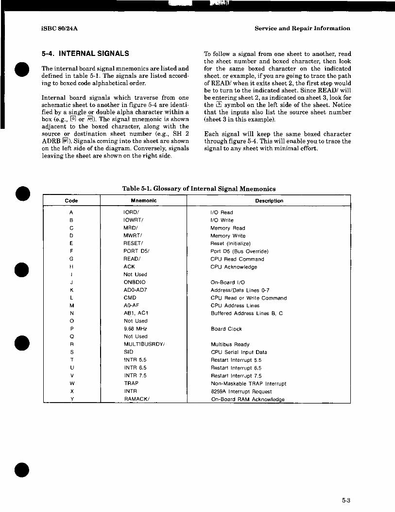
•
•
•
•
•
iSBC 80/24A
5-4. INTERNAL SIGNALS
The internal board signal mnemonics are listed and defined in table 5-1. The signals are listed according to boxed code alphabetical order.
Internal board signals which traverse from one schematic sheet to another in figure 5-4 are identified by a single or double alpha character within a box (e.g., @] or ~). The signal mnemonic is shown adjacent to the boxed character, along with the source or destination sheet number (e.g., SH 2 ADRB ~). Signals coming into the sheet are shown on the left side of the diagram. Conversely, signals leaving the sheet are shown on the right side.
Service and Repair Information
To follow a signal from one sheet to another, read the sheet number and boxed character, then look for the same boxed character on the indicated sheet. or example, if you are going to trace the path of READ/ when it exits sheet 2, the first step would be to turn to the indicated sheet. Since READ/ will be entering sheet 2, as indicated on sheet 3, look for the @] symbol on the left side of the sheet. Notice that the inputs also list the source sheet number (sheet 3 in this example).
Each signal will keep the same boxed character through figure 5-4. This will enable you to trace the signal to any sheet with minimal effort.
Table 5·1. Glossary of Internal Signal Mnemonics
Code Mnemonic Description
A 10RDI 1/0 Read
B 10WRTI 1/0 Write
C MRDI Memory Read
0 MWRT/ Memory Write
E RESET/ Reset (Initialize)
F PORT 05/ Port 05 (Bus Override)
G READI CPU Read Command H ACK CPU Acknowledge
I Not Used
J ON BOlO On-Board I/O
K ADO-AD7 Address/Data Lines 0-7
L CMD CPU Read or Write Command M AD-AF CPU Address Lines
N AB1, AC1 Buffered Address Lines B, C
0 Not Used
P 9.68 MHz Board Clock Q Not Used
R MUL TIBUSRDY / Multibus Ready
S SID CPU Serial Input Data
T INTR 5.5 Restart I nterru pt 5.5
U INTR 6.5 Restart I nterru pt 6.5
V INTR 7.5 Restart Interrupt 7.5
W TRAP Non-Maskable TRAP Interrupt
X INTR 8259A Interrupt Request Y RAMACK/ On-Board RAM Acknowledge
5-3
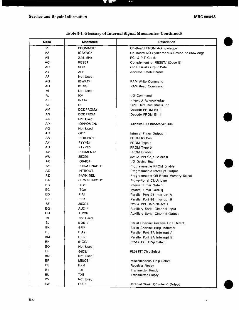
Service and Repair Information iSBC 80/24A
Table 5-1. Glossary of Internal Signal Mnemonics (Continued)
Code Mnemonic Description • Z PROMACKI On-Board PROM Acknowledge AA 10SYNCI On-Board 1/0 Synchronous Device Acknowledge AB 2.15 MHz PCI & PIT Clock
AC RESET Complement of RESET I (Code E)
AD SOD CPU Serial Output Data
AE ALE Address Latch Enable
AF Not Used
AG 85WRTI RAM Write Command AH 85RDI RAM Read Command AI Not Used
AJ 101 110 Command AK INTAI Interrupt Acknowledge AL S1 CPU Data Bus Status Pin AM DCDPROM2 Decode PROM Bit 2 AN DCDPROM1 Decode PROM Bit 1 AO Not Used • AP 10PROMENI Enables PIO Transceiver U36 AO Not Used
AR 0lT1 Interval Timer Output 1 AS PIOO-PIO? PROM/IO Bus AT PTYPE1 PROM Type 1 AU PTYPEO PROM Type 0 AV PROMENAI PROM Enable AW 55CSOI 8255A PPI Chjp Select 0 AX 100-107 1/0 Device Bus AY PROM ENABLE Programmable PROM Enable • AZ INTROUT Programmable Interrupt Output AZ BANK SEL Programmable Off-Board Memory Select BA CLOCK IN/OUT Bidirectional Clock Line BB ITG1 Interval Timer Gate 1 BC ITGO Interval Timer Gate O. BD PIA1 Parallel Port E6 Interrupt A BE PIB1 Parallel Port E6 Interrupt B BF 55CS11 8255A PPI Chip Select 1 BG AUX11 Auxiliary Serial Channel Input BH AUXOI Auxiliary Serial Channel Output • BI Not Used
BJ BDETI Serial Channel Receive Line Detect BK BRII Serial Channel Ring Indicator BL PIA2 Parallel Port EA Interrupt A BM PIB2 Parallel Port EA Interrupt B SN 51CSI 8251A PCI Chip Select BO Not Used BP 54CSI 8254 PIT Chip Select SO Not Used
BR MISCS/ Miscellaneous Chip Select BS RXR Receiver Ready BT TXR Transmitter Ready BU TXE Transmitter Empty BV Not Used BW OITO Interval Timer Counter 0 Output •
5-4

iSBC 80/24A Service and Repair Information
Table 5·1. Glossary of Internal Signal Mnemonics (Continued)
• Code Mnemonic Description
BX PORT D41 Clears PFIN Flip-Flop (U47. Sh. 9)
BY 59CSI 8259A PIC Chip Select
BZ MMCSOI Multimodule Chip Select 0
CA MMCS11 Multimodule Chip Select 1
CB MMCS21 Multimodule Chip Select 2
CC MMCS31 Multimodule Chip Select 3
CD IOP2ENI Enables Bus Transceiver U35
CE MMWAITI Multimodule WAIT Command
CF MMPRESENTI Multimodule Present
CG MIOINT 1 Multimodule Interrupt 1
CH MIOINT 0 Multimodule Interrupt 0
CI Not Used
CJ MIOINT 3 Multimodule Interrupt 3
CK MIOINT 2 Multimodule Interrupt 2
• CL IOASYNCI Multimodule Acknowledge
CM CLR Clear Counter U20
CN U31PU U31 Pull-Up Resistor
CO Not Used
CP A1 Address Line 1
CO Not Used
CR A2 Address Line 2:
CS A3-A9 Address Lines 3-9
CT AA, AD-AF Address Lines A, D-F
CU AB, AC Address Lines B, C
•
•
• 5-5/5-6

•
•
•
•
•
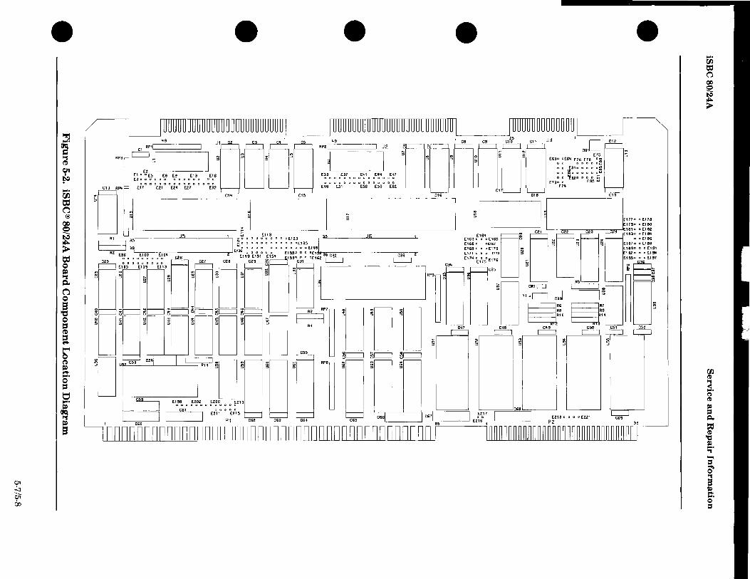
01 ~ Oi 00
• • • • • ~ ,~~~~~nmJUUUUll~~~U} ~IJ1]~~~~~~~~~~~~~u~~~~~~UUl I ~~~~~~~~~~~~~! ~ RP3~e::;'L' ~ :O~Dc, ;!;1~c'I.gA RP'r''"m I J2 ;;OU[j n' C. DC! -OC,'05 w[Cll J3 ,~[ D91UDc12 [ 9' E2 m~ I I I I ~ g; 5 0; 0; <630 om m E7. E:~ 5
~ , g:::: :: 0 '::: :':': 0 :':' lJ "'0 0 0'" 0 00'" 0 0"'0 0'" :: r.': : : : :l ~ sAP' ~ E17 Ell m E27 E32"" I [.' _ ~ 0 0,;,0 0 0 0';'0 ",;'0 0,. ," I J "' '" u;,;, '.0 0 ,.! '"
i L) 1 r "' " ",,-~ 'I I ;1 - ~; ~::;:,,:~ ~ ~ :c 1 ~::::::::: :E;';<135 J "'---- J6 :1 E'.';"O·'OE'05 n~ CC
., nOZ2 AOl' FlC"~::!: :~::;
,,"" ","0"'; 0 0 o. 0000000 oE". E' •• o 0"" ::::::;:; ooE' •• 7 ____ "_0_."_."'':.,'''_ .. E155DDDDE1636 E1680 ° o £170 0 ::::I ::::I ::::I £187
0D£188
it 6 C33 E171 " 0 D tl13 ~
J ~ I"P5 ca. .,,, °E,075 :::~ ~ .,
,~. __ ~ ~ CR'c:::J C
~[ [ ~[ [ ~r~ ~[ [ :J' ,
e53 os. [ .~ ~ . .. ~ ~,-----", ;,,-------, :ll ~ ~
-'I II II II I II I II I I I I II I
f I "'3 ~.o;.,o P,'oo ::;::: ~;:bJ Ld Ld II 1 I I I I I I. I I d - -. 9 I' eGO --=:=J P1 c., c.. os. ~ ~eG7[ ~ ;'0'7 [ [ ~ 't==J
nnnnnnnnnnnnnOllllnrnmnnnnnnnnnnnnnDllnnnnnnnn rm Em 1~~~~~~~~,~~~~~~~~~~~~~~~~~~~~~~5~
.... 00 I:l::t C 00 ~ ~
"" >
00 (I)
~ ... (') (I)
~ ~
1;' "CI I» ... ., ~ e' a a. ... o 1:1

•
•
•
•
•
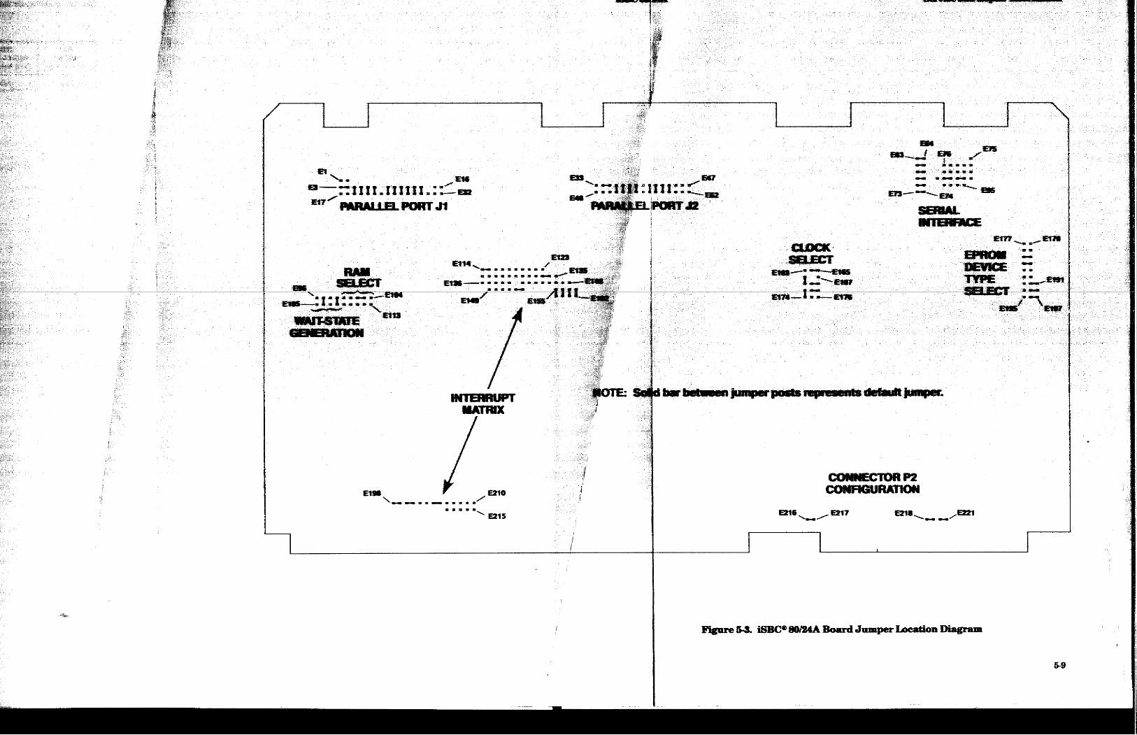


9' ,.... ,....
• ~ ~.
a ow ~ .... 00 I:Xj n
® (Xl o ~ ~
> I:Xj o ~ "S ~ 00 (') r 5! s. .... (')
'=' .... ~
(JQ "S ~
5! @ ;-(tI ..... .... o .... .... s
D.
C,
A
• POWER l '}I'"f C TlC\J5
Jw, T f~~F ~E217
... :'VAUX PC - 3,,4
P? -
1C14-16,47
1·1UF
• +5V AUX
t
;' ,,," : ,~ I"
( _ j I· 1
C~~10)121317 !
+ C59,67 I 45-51>53 ~6-55)40'-46 Ill'" ,~ " , o,~",,;~
(-,'-!('UNO P2 cl.ZZ
p1 - 3,4
+:::\/ P1 - 5,(:;
1'1
+ 12.v P1-7,5
- 5V P1-9,10
- 121,' P1-/9)t30
~ P1-1,2 §4 GROUND
l
NOTES, I"NL C ·THERWISE SPECIFIED: 1 R.E:5IST2R VAL u[S ARE IN OHMS, ',,4W i 5%
+ I CbO
T 2:ZUF 15\1
lc.e ruc
+12.V
-'
• - ~v
.1 ~~tF I C11 • T 15V I.,uF -12'V
2 CAPACI-;-OR VALUeS AR=. ~,1ICRC F;>"RAD5 +00/., -Z0:~, 50v. @] ALL 24 PIN PARTS USt- = ,,~,0CKET5 XU52 THRU xu~'~
BE IN5ERTED WITH PIN 1 'J THE ?4 PIN I.e. IN PIN ~' ?8 PIN SOCKET.
4. UZ THRU us, U7 THRU l_'~v' ,52 - U55 A.RE 5HONN FO;::;: ',"tAPJT'v' ACTUAL COMPONENTS r·Y·i[ ,,:,,_,STOMER INSTALLED"
f5l ODD PINS ON ')1 AND ,? ARE ALL GROUNDED. [!] IMPROPERLY iN5TALLEO ':::C'NNt-CTOR.5 (.J"I,J2. AND
IN DAMAGE WHEN JUMPER::, C2 - E:1, E33-E45, OR [50 - E75 ARE IN5-:-A!._L.Eu.
• • A t?L-r
B KG
I REFERENCE DEVICETABI t
DEVICE POlA"R f;l~ UNUSED LOGIC I DESIGNATION TYPE 6ND +5V +1ZV =SV' -1?VI+5VAUX ELEMENT OUTPUT PIN5
UZ7 74L$0Q) 7 14 U56 74502 14 -uZ2 7404 14 U22 -5
u3346 74504 7 r-w-- 1 U33~6JU46-4 -U25 74L504 7 14 U35,41,44 74L5Q':15 7 14 r--I-- l' cCO ',",'< U4il' 74LS10 7 14 lIc6 ~ ....... 7 14
-.. )29,4345 7 '4 -
U30,42' 74! 53, 7 14 U42 11 --
usa 74536 7 14 - ---
U31 41 74LS74A 7 14 I-- -
U39 /4L.51? :') 10 16 U4e 745 ' 3E 10 16
, -
U2.e,-5e' 74,_ SUB 5 16 - -
U49 745139 5 16 U14 740140 7 14 U5963 74L5Z40 10 20 U37 74365 5 16 U37-5 19 U64 745373 10 20 UZ0 74L5393 ~ -U60-62 74ALSS50 10 20 U12 1455 7 14 1 U1113 1459 ' 7 14 US? 3215 14 U3Z 362:5A 1 9 15 U51 6264 -15 14 ?,""-,
U34 e085A 2 20 40 U21 e22.4 8 16 U19 eZ51A 4 26 l'15 52'S:'! - 2 24
, b2~5A 7 26
"6 ~~~~A 14 210 ._-U::,5,36 10 20
-l11)6
~EC 10 20 j,UZ - 5 7 14
- -
XlJ7-'0 SOCKo 7 14 ,Xll~Z-~)5 5(:.(.'E 14 ~B
-
""$O'",_'''~O'~ ~~ DRNBVA PEAKe s ~
~GYICKleft.li ~ri; I ,'" ,- .. I"/i'
inte/" SO---1, ssc 60/Z4A
--I
... 00 t:xl ~ OD e ~ ~
>
00 (D
~ ... (') (tI
~ =.. ~ ~
= ... "S 1-4 ::I 0-"l a ~ ... o ::I

Service and Repair Information iSBCBO/24A
ISBC iSBC 80/24A 80/24A Sheet Function Section
Jumper Pair Grid Reference Ref. • E198-199* 2-A6 Connects 9.68 MHz SCLKI to P1-13 (output) 4-3
E200-201 * 2-03 Connects SPROt to PH6 (output) 2-19
E202-203 2-06 Connects AACKt to iSBC 80t24A board via P1-25 (input) None
E204-20S* 2-A6 Connects 9.68 MHz CCLKI to P1-31 (output) 4-3
•
•
•
• 5-12

01 ~ c:."
• ~ ....
i ~ .... rn t:= (') ®
(X)
~ t:= Q
~ rn (')
t:r' tD a a. .... (')
t:I .... $I)
~ s ,-., rn
[ t.:l Q .... I-l
8
D
c
B
A
7
• ~<;"v
,
6
RP7 'OK
5
• • • " 3
-:.e.e. c::,\-\SE."T Q\o...lS
to....~c.'U -z..rc\ EZ030 ~.--~4\\ r"l.. U43
X~K/ 2~: ~y~,-~ ~v ~\. ~IMUQ"\e.~Qt:H'/ ~~~ ~~~~"2.
~oC..Q\...l"T~O\..l....E'Q. US? ~ ! "',
~~/\~~------------~--------------~~ ~~ l.CRD/ ~ ,,' ~\
~~ ~ !1I~~-==r~=-~-,::::::::::::::::-=-;-=-=-=~E~C~0~,""tCC~0~W::~~~~~\U ~?~/ "S143 MRDI \I B.l.J"'S"-{/ ~'"eo M~/ 18 SQ.E.GV '"5\;~ 12E.'SE""I' / ,q M;;u:)C. /
)2.0 l'-"I"W"'\c,/ )'2.,.\ l.~c../
"Z.'Z. Io.NC./
..... ..., =CF>I l£J
8H.3 U31 PU ~
..... .", ",a..:.;~
~~ I:l...c.v:::. ffi ~~e O\.J9.D'I.O .;
.,...,." .... '=>0-"""'-., Qg
~." CHC [hJ-
~'"" .... "-'2l
~~LS~ 4 USB L<o
U25 .:; ~~e, '"2,.<::;' ca~/
~ ~L ."'-~ ~ ~ !!!.
----<:l '" DO>.\'0/- ·DAo.'T7/ r-
. . __ ... --_._.-. ......
~~t:>~E.'R"::, PI
0I\Ir0..'Tcz,/
] '/ ?/ 3/
4/
"/ G./
DIao.""T"7/
i3 J
'" A2 OR
A'3- 0,5 @J---SH3 AA, AO- AF @}-J
"",", "" "
58 os'" , .... )cs.~
----------==============)~ ~~ ,-~' SHT e
A.CrR~~ 2/ 3/
I
'! ~; (,,/
7/
B/
II ~~
s,,~
• 7
~NEJ;;t.. /IIoJ
-------- ~
"M" I: l '" ---'=-t'
B/ C/ D/
• E/ ~F/
P',
I _======================================================~)\3 BCLK/ L )~\ CC~K/
6 5 " 3
B
D
c
B
A
.... 00 ~ n 00 ~ ~ ,::..
>
00 til
:! ... (':> til 11:1 =:s c.. ~ ttl
'CI e. '1
"'"' =:s 0-a a ... o =:s

Service and Repair Information iSBC 80/24A
iSBC iSBC 80/24A 80/24A Sheet Function Section
Jumper Pair Grid Reference Ref. • E96-105 3-C5 Connect for 4.84 MHz clock only 4-3
E97-106* 3-B6 Enables failsafe timer 4-35
E98-107 3-B7 Reserved None
E99-1 08 * 3-B7 Connects RAMACKI to READY gate 4-29
E163-166 3-05 4.84 MHz Clock input to 80S5A-2 CPU 4-3
E166-16S* 3-05 9.68 MHz Clock input to SOS5A-2 CPU 4-3
E171-174 * 3-06 Connects 8224 output to divider network None
E21S-219* 3-B2 Connects INTAI to P2-36 (output) 4-23
E220-221 * 3-A2 Connects BMTO to P2-34 (output) 4-34
•
•
•
• 5-14

01 ..:.. 01
• I'2j .... ~ = ~ 01
~ .... 00 t:C <:i ®
<Xl
~ "'" > t:C o e; r:l. 00 ()
=('0
= a. .... ()
t:; .... I» ~ "i I»
= @ ; ('0
"" ~ o .... .... 8
D
-
c
-+
B
-
AI
• • • • 8 I 7 1 6 I 5 i • J
=..~~== ar.naOOlll'OlW'lOllnn_
~~ ~RP6"~V :#'0 l R6 '9;~3bMe~ -u~: ~7<~ , ~
,- 0 I 'Z I ... ."v. ~~~~ +5'1 -::!::- 81;0 I
7404 F RB R12 • IS 74LS39~ -;::;- '2. ~e~l. R4 p~ ~ Ci:2.1 19~2!l.~I~ EP1 1 Q~ L166 111'-..10 \ ~?a f]...
IN914B 0'50C, A XI ~\~
3 If"""" TI"'l
'SS,e. "::.'t4.e;EI Q\..Je..
A.e. 1..\'5, M~~ ':Io~'"
CoM c.L.12. '5~' ~ q.(pe.M~~ ~"Z.)IO
~~ Ra-s&"T ~~.IiQ)1J!O
&. ~~\/ -a""",-~ 'SOC ~(,p
CU AB,AC g\.j4,'B
AA,AD-Af gJ4 2,4,B
,tc fl CO "'- CLl>. ", E'n') C03 "'" '"
~~ l,7' "~Ei'74<> "Ql!,f"--~ "'~ i: U33 J 1'4 ~ ... ec pz.. 2- 5221 _0 QCP- \"""Mliz ,~Cj><>. I~ />.C
~UX~E,/ ~ ~·T· ~~ QD~ 7.:1,.0::.04 I 1"2,. n ~C 'CQ~ C39~~ P II 7\:Zi."!:':i2. "~ \1 CA. .e...e ~u:>1C:. I
IC).F-J"'''''' ...,. I.~'" ,UOB 10.:0 '"'" [J ~ CS A 3-ra .91-1.2,4
",*,,,,
... "" -'" '5PI"I -.. """'" SI·HB
H . .\\l/ ,=>,t::>
\\...ITR.'=::..=:O 1~"T~£..:"cs»
1,,""R.7.~
, ..... ? ,..,.,. .... to5VNC I
1 - \0 '2"'!> ~n ~~ - RP7 U2':9 'Z.\ Irro.P. ~ Y \01<. 7 ,<3,,,",,,'0 U33 U3B 1 .. 6 'co..." 'eo", Q ,., "t t .. -,j~
",I t '<f>:l.-~4 """" r Ie..~ \""l 1''- ~ r.:;,;J I .;?:. ra.-~ c:, QSflIJ ~ \-, ~ ~ \~" ,b.,t::;, ~ ~ ~Slt:l <3,.'(.£0 ~ \~ Ub4 I" <:) ~,
T e :T1io.C; ~, ~ e q s.bt..~
~ -, (". . ., ~ \4. ~"2.. "'7 ~ -, ",e. ....f"'CRl A2. ~ ~ tc, \ ~ A..\:) \ 4- 0:; ~ .... \ rep! At ~ \O~ "C0 1"1.. Il000 3 D Q ~ ~,.,m ~ A(J) ~ +;v I\,J'TQ. ~U~-:z. ~ c;,. ,~
SHl 2,<4,10 5HT 2,+,5.".7.'0 SI-lT 2 J4/5J b, 7,':))10
I074S2.~ l'RFB "L.E ~ 74~ ~ ~ 12 10K. U34 I ~ 5 10 U4~ eooII'!.M. "- I M;>0-.... 'C7 """<.49
u20 6n,' f' .. ~ ""'" ~U2L,,·-o¥ ' •
, 74~~C. E76 "lollSlll '0~ 74a>-+ "5_~~ ~"'!:il... ~ ,.." ~ ~'"2. 'lJ'-1O ""'04. ~ -....<:>? ""","2..
P-o I 'I-O..e \~ flJ46~"74~ : ~<=;:'~"2.. ~ I
SH4 RAMACKI ~-r-+sv
I U25 I rr ~ l -~~ , /lo... J:OR.t:>;' ~"2...)"5IU:>."1'.q;l\O
~t)lIo.. !"" <..,1 r-=---"1
U44 ~ J. : ~~'T/ ~')-:'){,p,"1'.q,\O ~~e I'~, <;,\-\8 """"'"" .... CO m,---~,--~i~~:~~~L§:dQ;o::::t-i----t---' 'U"Y£."00i~
1 L-.. I I ~"!. :~ \I: C MI<.O/ "=*"
~ I pLJ t"''' U44." 1 ~ +5V __ . I I ..,.;~ ~,i \J~~ ~~'W'Q.l/ ~"2..
• R9 (::1<::'. i'" IOtc:. U45 ~------,-t +511 ~ "301 'f ~ 1'Co.I.-~0~ .e..c::. ~\.I.J"Q"T/ ~4
22.,,- 1_1uF ~~~ 1 12.~ 4~-
'I·o';':! . ~ +5v "" '". tPt ~ I I~:c..:. ~" L c:.MO .... n.,-,,6 7 ,-,2'16 I ~ ~"l. I _1:i.. ~~~
I ~~----·-L': EC7 E1wk I lJ!5b 5 'iilt) ,I,.). e':t~ '!!:.'W).. Q---' ,-) RJ=l4. """ ':to/' ~"",~,,, I e.
0) ~39 112 'L'r-45 10k. qU56 ')314- h \\ 4--,a.~~"2.. ""21~ E219 ~~~ I\...n""~/ I 1:(; . _ +:)v ,,'Z. D Q c:,. l'I..l'TA...--l-L-J'30 ~ \\.S,.c:..,,/ 5~e,q
-L,---:"2~. 11 .... 502 '374l574A. 1..0 -!- U;'_'7 ~ -,
I ~t I I I, U2b ,'''''' CL ... '"" I L '!>, f:l~ L -" ~4 . ~ "'" "'''''',-','' 1K Lf9. \ +"W '!:00 ~u 74-L~"'74A ---, I 7'SZ~ U27 ~,P(' I r.-__" I c;;:,\ ~ "2 t:> Q "-- UC 6 I I .. .... ~ 1 ........... u.J1 t.l47
51-12. MUlTIBU5RDY/~ I I I ! - ==.l /(l,.L~~"2.. ~ ~ ~ ~~ I ~e ~~I...\/ ~rlT e. JOA5'rNCI rcLl- lK 1 I c.1-~ ~ ,4~
I I "'R21,
II ,'''-
, ~ [8.] "'-0.1<:. """ ... E221~ ----)?'2..~ 'O""'\t--"D
I I """ " U31 PU ~ c:.pu COI-'I"""-lD .... """" G.a.lEQI:Io....\"\O\.j, ~E:\..lE.R~\Qtl....l
1= c..p.u,\\I-"\\~,~ ~
2 !!J-'wof~li '1'2 If !SIIm" ?.
8 7 6 5 t • 3 I
D
I--
c
j+-
B
I-
IA
.... 00 t:= C')
i
00
~ .... ~ ~
~ Q..
~ 'C:S I» .... ., S' a-S a .... o =

I,' I111
Service and Repair Information iSBC 80/24A
iSBC iSBC 80/24A 80/24A Sheet Funclion Section
Jumper Pair Grid Reference Ref. • E1 02-1 03 * 4-C5 Indicates default RAM space: EOOO-FFFH (SK) 2-12
E102-103 * 4-C5 RAM address matrix. See table 2-4 2-12
E103-104
E111-112
E112-113
E100-109 4-C7 RAM size jumper. See table 2-4 2-12
E101-110 4-C7 RAM size jumper. See table 2-4 2-12
E177-197 4-86 EPROM device type select matrix 2-S
•
•
•
• 5-16

01 ~ -.:J
• ~ .... ~ ~ C1I
~ .... 00 t::C ~ ®
~ ~
> t::C o ~ ~ 00 ~
go 9 I» .... .... ~
t:; .... I»
~ I» 9 @
r ('D .... ~ o ...., .... 9
D
cl
....
•
-
A
• • • • 6 1 I 7
-T 5 • I 3 I fiii1ir 4
~~ae.""'OUE
~.",
~~ U51
~~ Ai 1~ ~~'! \0 ~ ~~ ~~~ A2 5 AZ 12 13 ADZ
"H3 AB,.lIC cu SH3 AA,AD- AF CT ro.lt3 A-3-A9 cs SH3 A2 CR GH3 Al CP
"5>< .... N1J ,.., ~" .... :1:0/ <>.l
-;,,,e. l"I>I::Ml>.C""~
"EMS DCD""",",7.~ 'SMe. ~'U~\~
..,,, ... ~O~eiJ,1
'SIr\~ '"!::o\
A3 1 A3 ::> 15 _ AC'3
U28 /\.4 (;, v u;-. ',D .. 4. ,-----,::---r.o.&.~__++--.,ii A5 5 ~; ~ lL_B.Qi..
A6 4 A6 6 1b AD6 A7 3 A7 r/071 AD?,
Q."2.. Ab 25 A6 \"'::.-.:: A9 24 A9
~E109 E10e /\A 21 AA
AB E101 AB 2.3 AB EH0 AC 2
y-----'c:'<jWE* L--+_--'~OE '
;----t--~'<jCS.l ..
~ ____ -t_~~_~~~ _________ ~1,U3B LC~S~2~~~ --"Ivv-----+-'+t------------~2"_L 6264 - 15
74 LS;;:'5 '----~--------------------------_I Ri.M £:,.(y./ SH3
.. 5V +5V
~.~."v
vee'l.S ti '"'2:1t.,,4(1.B?IU) cos T7
P>C.. ~~U52. -~=~-r-':5~---~k:--t::...<Z) l0a...<z:,--- ~ ~
Ao..\ q I \\ Ciftn0 "'~I ?to<Zl-P\O"'7 ~"7 ~ e~ on ~\ ~ ... "'!:, -, ~ I I' \~ Pto, .e..4 (g 4 "4"ioe.,"l."-:tC. " IS ~ I:a.~ C) ~ '''\!''#)''2.I~''2... \(,.;, J=II\04. ,.,., 4 <... ('2..4'P\~ .. i) 4\, ~ ... , .., ~ "'lie PICe. IIo.e, -z.-; B 'A Pi07
I - ~~J~J~~n
~I-J U42
• D
f-
c
I-
•
A
---~ ItSa\.UI 11CAlL !\.¥?\..1E:.. ISHW 4
I 1 I • 7 6 5 t 4
.... 00 to C
~ t
00 ~ ., <: ... () ~
~ ::I ~
=c ('D 'tl ~ .... ., 9' 0-., a a .... o ::I

Service and Repair Information iSBC80/24A
iSBC iSBC 80/24A 80/24A Sheet Function Section
Jumper Pair Grid Reference Ref. • E1-2 5-B2 Connects + 5 volts to J 1-50 None
E3-4* 5-C4 Configures port E4 bus transceiver to input mode 2-14
E4-18 5-C4 Configures port E4 bus transceiver to output mode 2-14
E5-19 * 5-C4 Connects port E6, bit 0 to driver/terminator 2-14
ES-20* 5-C4 Connects port ES, bit 1 to driver/terminator 2-14
E7-21 * 5-C4 Connects port ES, bit 2 to driver/terminator 2-14
E8-22* 5-C4 Connects port E6, bit 3 to driver/terminator 2-14
E9-24* 5-C4 Connects port E6, bit 4 to driver/terminator 2-14
E10-25* 5-C4 Connects port ES, bit 5 to driver/terminator 2-14
E11-2S* 5-C4 Connects port ES, bit S to driver/terminator 2-14
E12-27* 5-C4 Connects port ES, bit 7 to driver/terminator 2-14
E13-2S* 5-C4 Applies + 5 volts to timer gate 0 (ITGO) None
E14-29* 5-C4 Applies + 5 volts to timer gate 1 (ITG 1) None
E15-30 5-C4 Connects timer 1 output to timer input matrix 2-11
E15-XX 5-C4 Connects selected J1 bit to timer input matrix 2-11 • E16-XX 5-C4 Connects INTROUT/BANKSEL to selected E6 bit 2-11
E17-19 5-C4 Connects port ES, bit 0 to PIA 1 2-14
E22-23 5-C4 Connects port E6, bit 3 to PIB1 2-14
E31-XX 5-C4 Connects PFSR/ to selected E6 bit 2-22
E32-XX 5-C4 Connects PROM ENABLE to selected E6 bit 2-11
•
•
• 5-18

iSBC 80/24A
•
..
•
• '"
•
•
Service and Repair Information
8-4.i
u
u
•
~ -, I~ ,------_A ----~
€I-r' t/\,r Ifl-''' ~ - r' ill
• Figure 5-4. iSBC® 80/24A Board Schematic Diagram (Sheet 5 of 10)
..
•
5-19

Service and Repair Information iSBCSO/24A
Isec iSeC 80/24A 80/24A Sheet Function Section
Jumper Pair Grid Reference Ref. • E33-4B 6-B2 Connects + S volts to J2-S0 None
E34-3S* 6-C4 Configures port EB bus transceiver to input mode 2-14
E3S-S0 6-C4 Configures port EB bus transceiver to output mode 2-14
E36-S1 * 6-C4 Connects port EA, bit 0 to driver/terminator socket 2-14
E37-S2* 6-C4 Connects port EA, bit 1 to driver/terminator socket 2-14
E3B-S3* 6-C4 Connects port EA, bit 2 to driver/terminator socket 2-14
E39-S4* 6-C4 Connects port EA, bit 3 to driver/terminator socket 2-14
E40-XX 6-C4 Ground post 2-14
E41-S6* 6-C4 Connects port EA, bit 4 to driver/terminator socket 2-14
E42-S7* 6-C4 Connects port EA, bit S to driverlterminator socket 2-14
E43-SB* 6-C4 Connects port EA, bit 6 to driver/terminator socket 2-14
E44-S9* 6-C4 Connects port EA, bit 7 to driver/terminator socket 2-14
E4S-XX 6-C4 Connects BDET/ to selected EA bit 2-14
E46-XX 6-C4 Connects BRII to selected EA bit 2-14
E47-XX 6-C4 Connects AUXO/ to selected EA bit 2-14
E49-S1 6-C4 Connects port EA, bit 0 to PIA2 2-14 • ES4-SS 6-C4 Connects port EA, bit 3 to PIB2 2-14
E60-XX 6-C4 Connects SOD to selected EA bit 2-14
E61-XX 6-C4 Connect SID to selected EA bit 2-14
E62-XX 6-C4 Connects AUX1/ to selected EA bit 2-14
•
•
• 5-20

iSBC 80/24A
• I §
I
~
l
:d 3 I ~ ~
II m I I -I
...
• -
..
• 1ft
-
• -
...
-
• I •
Q I u
J
~ til ~ ~ ,
III
~ f}
0 ~ ~
, A
r- ..'I til '1 til rJ -
{I ~
.H r 1f13Jroro::31f1
> ± '\'
-P:eI1 ~~~~"~r~ ';=--- J
~~ 0EID~ ~ '" £) " "" § ~~X ~ ~ !i~ ~El- , ~itli o ~ iJ .{ . g H fI~ r:
~ j/l1fi" 1r~ tft ~61 l oJI~1fI ~ ~~ ~ ~ ~
Q I u
~ •
OJ ill
~ ~0,
El-"'IfI<ttl'-'lr-
QII g~j ~. ~-"----'AA---t-H-l--t-1O<t1l' -=, t
...
t
,. "
•
fl
Service and Repair Information
I -C
,p~
~~ . '.
(J' i J(J' ". ill r J
~ if ~ uI -
~ ; A ,r- I-
- " IfI <t II' .9 ,-
,..
...
I' "
--
1ft
...
-
•
I I ..
Figure 5-4. iSBC® 80/24A Board Schematic Diagram (Sheet 6 of 10)
5-21
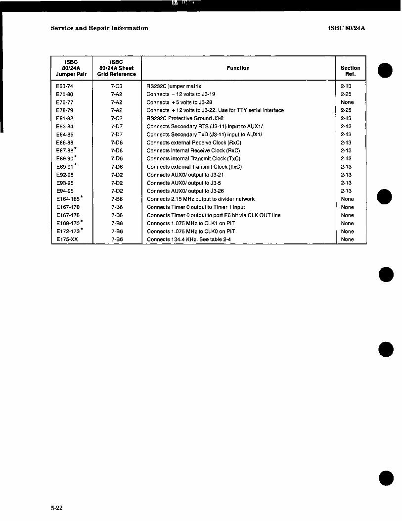
Service and Repair Information iSBC80/24A
iSBC iSBC 80/24A 80/24A Sheet Function Section
Jumper Pair Grid Reference Ref. • E63-74 7-C3 RS232C jumper matrix 2-13
E75-80 7-A2 Connects -12 volts to J3-19 2-25
E76-77 7-A2 Connects + 5 volts to J3-23 None
E78-79 7-A2 Connects + 12 volts to J3-22. Use for TTY serial interface 2-25
E81-82 7-C2 RS232C Protective Ground J3-2 2-13
E83-84 7-D7 Connects Secondary RTS (J3-11) input to AUX11 2-13
E84-85 7-D7 Connects Secondary TxD (J3-11) input to AUX11 2-13
E86-88 7-06 Connects external Receive Clock (RxC) 2-13
ES7-SS* 7-06 Connects internal Receive Clock (RxC) 2-13
ES9-90* 7-06 Connects internal Transmit Clock (TxC) 2-13
ES9-91 * 7-06 Connects external Transmit Clock (TxC) 2-13
E92-95 7-02 Connects AUXOI output to J3-21 2-13
E93-95 7-02 Connects AUXOI output to J3-5 2-13
E94-95 7-02 Connects AUXOI output to J3-26 2-13
E164-165* 7-86 Connects 2.15 MHz output to divider network None • E167-170 7-86 Connects Timer 0 output to Timer 1 input None
E167-176 7-86 Connects Timer 0 output to port E6 bit via ClK OUT line None
E169-170* 7-86 Connects 1.075 MHz to ClK1 on PIT None
E172-173 * 7-86 Connects 1.075 MHz to ClKO on PIT None
E175-XX 7-86 Connects 134.4 KHz. See table 2-4 None
•
•
• 5-22

Cll t:.:. ~ ~
• ~ ...
(JQ
= "i ID ~
~ ... 00 t:C n
@
(XI
~ ~
:> t:C o = "i Q..
00 ~
go 9 ~ ... ~
t:;j ... = (JQ "i
= 9 00 =ID
~ 'I o .... ,... 8
D
c
•
A
• • • 7 6 5 .. :I
'"E:.eE. ~1!:.ET 0\..1Ei.
,""'" J~ 1\ RIWC":.: \~\C.b..\O~ \I u~ L-fli.. :~ :~;/
'R.E.c..L\~et:>El 1(0 "0" e U12 8C!:I ~X\/
o'E-BL U; ~ '"
_1.# ... ... '" ~'"
• "5=.E.c,lZ\'S. \1 ( ~30, U\'. Vfe I ~
'SEc.."'~I....I"S.t;)j:I..'"'(.o.. \ ( -5"0 U'3"1'l.. I I :'ee ~ o;q,c;~,,, J~ ~c..CT~ E9~ ~=:, CSE.czac.~A..
f ll4~ .;.'!>v 12.(0 ,14eB ----, l ~"2..\ ~c:.~\G.E.LE.T\H\\ .. .I(_ .A.,UX«?/ BH. \4.E'R I...f' ~ ~..,. \~ I "2. ~ XM'T I(. 3J.r- \"3~C91 U\, 1'- RXD xc I l _ 65 ~~ ~-: CD Q.1!!!c.. ~/::Io.,.
'S\-\,(p
""""eo .......... ... ,,~ =i RX"
"'*'''' IT \,XR """'" IoU ,XE ""'", s""
c.~ lk" 1"1. ~ 4 (,s> "2..'2.. 'lA- I 4 L --' l_~ c~ )4. "TQ..I:o..\-..l"5:.t)I:Io.\"bo..
CE59 un '1<; t::6Q.. Di~iI?1 }v: ~_(1 E7i \"2.. ~
@=561Ior--eo Ii "Z.~ I~ ~E74 I"!:. crr;a \4~ ~'7 J469 ll'~"";o, CT'SoU19rcr<S IT 11...1 'J: 1\ I f:,(d..QOE 70, )ID C'TS
J~ ~- 0- . ; '----L-/ I F"(; 1 F h8
QEC.CJ...K. ., ( U1';t~"'" 0";56 ~ TXC. L U 1 Z- -- eo ~S ? ~~~w~
= _"",>4-C:;\C.-:"/ ~ ,~c.o::. ~D; ~- -ta= ~=-;/ ~ ~ ~lXewN~ ~ ~..,.. ~ -z..1 1t&~"'\ I s" ... ......... ........
SH3
?-.l .... MH!. ~ 0 c.~ ~~00.'O'l.0"'1 ~ PD
C.Le: ~ n.. ~ r :' """"'""=Ne.",C":> \4 G!~O
"2..~G~t::I
.... e ... ".",
sH3 ....... e, .........
SI-\",
"""'" "'1-\", 5 ... ",
8
iE165 I~ C\..R. QA.. II ~ ElM r Q~b9. 1 110170 II~' ,-, " , " , ~V\SR'S
~ I!!C.I' "-0/
l'1L'5~~ I J~ ~ E167 'W ----- -
""0"1 eI~ ~ ;,,~ ~ 1"" ~c,I!5 "'" Pl:oc;. ~ 4 & "",0 ," 4. ~O(l)-~- P.I:or I (P
~ crT 1 'S4=;')Q 6W Q1:.'fZ) ~
U en ~ 111111 l2.t) az.~ _ , n~ OIl"'"!:. ~ , \ c:.uc::'2.. 012)1 10 ,'"
S4c:o=./~ f>.JZJ M t:o.. \ c? rT~(z) Be.
III L ,"> Cu<' l/::o..CZ> \,-------------. I~ q 0-"-1Zl
/:00..\ "Z. ~ y~ \4 t:a..0 ~ ~ "'- ~c i,~ I I ... , w~
Il' 1"3=>\f \\~\E0
I"Tc::=.1 i!.i!:,
"'-,
~ ... la.~ I I --- 14Gi~=\ I M~;/~ ~~~ _;~ I i I --+- ~v~ I c'"'''' LC::J- (p "'" Y7 OJ- II I
~
~.,,,
P"Z.. t~l1 PI=oSJ/If( ~£.40
7 6 5
PORT n~
.. :I
-5V f " l'7"O ... E-" 0
~
-,-tv ~
1.
~ \:Ie.
I=I~~ , ,,~
m CL't(.OVT/r..\.J. c:.'rI.":> ?C)Q'T t:A-1 s;.q PC::>Q:.Tt:>=;J' ~"2...
~~;,....'?O~ "'i\~'R"'S
D
c
•
A
.... 00 I:l:j ~
~ t-:l
~
00 ~
~ (;. ~
III 1:1 ~
::tl ~
'l:j III ... "1 ..... 1:1 go a III .... ... o 1:1

•
•
•
•
•
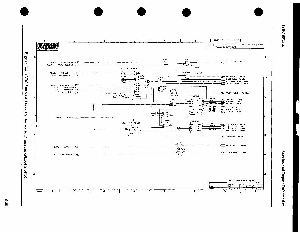
01 t\:> 01
• ~ .... ~ ~ 01
~ .... 00 c::I C":l
@!
C1J
~ > c::I o 1» '1 i:)..
00 ~
g' 9 ~ .... ~
t:I .... 1»
(JQ '1 1» 9 --00 ::r ~ a C1J o "*' I-'
S
D
cl
•
A
• • • 7 6 5 4 3
~e. ~E.e.'T CJtt...1E
cJ46 u~,
"'!!.\-\\O MM~\"'T/~ ~-- c!.. IOA'ElYtJ.cl 6'"'3
cs.~=; ~B.lI::rr..l!oL.E f;l...y 745(1)4- 749$2 ___ '>V
t:£Co<:a"""""",, " l--o - r- I ~ :; I U.3L ~ 'to 5YUC./ ~ ... Ii'~ [~~ ~ I~3(;2.5.tH O"I..J.E.C'I.O ~'.-I,.~
.0...._ ~ 4 0\ \4 t>..~ cc.t::Io ~l-"\ "'!.\pI,,4 ~ 'Z p..-, az. \"!o DC.t>~l-"\L.. ~
~~ AB.AC C;;H3 AA.AO-D.F
""*I'D MM~'E."_iT/I'
~ :il~ ~,~ i '51-\4. I"TYPECZ> ~4 I"'TYO>E: , ...... .", IO, ~ -~
,
~ ......... CMO
I U<11
-----f------ITJ """"",,,,c.,,,, "=*,"'A
/lA.s.\~
... ,,"> ... ,,'" -'" -, ",","", ... ,,-,
I ... ct».C1 B~ ~"",,c."=:.<t>/ "=""'10
C) c.e.-c:.F c..1:>.. ! I \ / '5.'1-1.\0 <.. F<Z>-~~ ca "Z../ ~\O
, i F~-~l= c.c. MMC.CS ~J' S\o4. 10
'SO'"2-
......... ~ ... , ~ ~~----------------~~~O~L~~' s,,<>
I i"4L~e. i 10 """"'""s"''''' ~f-_______________________________ =-:>De ~ !.O~E.\..l1
1).-1' S"'4
.......
•
DEc.ot::E.~~c.'K~\
• 7 6 s 4 3
D
c
•
A
.... 00 t:C C"}
~ "" >
00 (!)
~ .... ~ (!)
III
= ~ ~ (!)
"CI III .... ., .....
~ e III .... .... o 1:1

Service and Repair Information iSBC 80/24A
iSBC iSBC 80/24A 80/24A Sheet Function Section
Jumper Pair Grid Reference Ref. • E114-115 * 9-B4 Connects IR7 to ground None
E114-135, 9-C4 Interrupt Jumper Matrix. See table 2-7 None
E138-146,
E149-162 9-C4
E133-134 * 9-C4 Connects INT1/to IR1 on PIC None
E153-154 * 9-C4 Connects OITO to IR2 on PIC None
E206-211 9-C5 Connects INTROUT/BANKSEL to P1-28 (ADR10/) output 4-7
•
•
•
• 5-26

at t\:, -l
• ~ .... ~ ~
~ .... rJ).
t:C n IS
~ ~ = Q
~ ~ rJ). (')
r e a. .... (')
~ .... ~ e -rJ).
[ cc Q
'"" ~ s
D
c
81
A
5H, 5H7
... "'..,
OIT I 0;"T0 ~
• 7
• 6 5
~ ~\ /4L~~
2"'1 !~ : mi 3/ <C\.O~ E205 '21 ~( 2 '7 1/ 4, E21(l
:t:\o..iTQ:V Q.\ E215 ~\/ZI/ "Z8( E211 0
:I.\.,fTVil.OJT! ~c.. ~ ~"""'-
PI
~ "'~~(------------------~
• • • 3
"5.E.E~~'O~e:.
U46 I I I I I I I I I I I 4 • ~ 20Q)-IQ"7 ""'''',,",,10
1"1 I' ~I ~I ~I §I ~I ~I ~I ~I ~I II 0:<~ DJ"T I' ~.",
I~
~ ... 10"" "= ="" 101
'T ]"" ""'.,. 1= q '2. 1."1.0 ""',. 'La'" 8 ~ 32.1 ,...,.. 1:04 "7 4 .o..'Z.2 ... """ :to"> ~ Ii» C;'Z."!Io
""""" ""'" C; <.. Ir:a.c."24 ..",.., XO"1 "0-'
b.l:>a)-...., I I( f-I ----~41__l.~--,_''''''''---___7
OE .,. U16 GO I --..
~ ... ~& ~I ~ S\ ,flo.\.,
~" 'I.~Aoo.I br..."; ~e ~S./ i! _ ...
p.Jl) I ~'" "'".", =W=/cg
s;'!. I()IC:CI /.l _ ... ""' ... ,
~"'C; ""'a 1
""'''' f'I"'-?. """"- =eo .. 61410 WlIDINT 2.
I I '" 51110 MIOINT!
~ "~
t£t -+ 5')
P'Z.. 1'1 .~~'7 e 'PF:tUI Iq( ~ ~37
E1~
E134 E153 E13 E131 E130 Ei29
0159~=150 E160 ~. E161 c 1 7 E.162 E"''''3-
.~~
~ E1~B
"""-, 5.H7
"", E;W7
~t:>'o-/ I'" 74368 'fii'7--------------------~~--.0, ~E = -~ ~I I
• 7 6 5 • 3
i :t""""""" u D.JTR (.c..~ V 'D-l-n:ot.I.~
W~
I::;j~~;-·j
......, .... .", -.", ~
\\.l"TE.~t:=rT'~Qi...I....lIL'Q.
D
c
8
A
... 00 t:I:I ~
~ ~ ..... >
00 ~
~ ff III 1:1 Q..
~ ~ 't:I el. '1
~ eo [ .... §

Service and Repair Information iSBC 80/24A
isac Isac 80/24A 80/24A Sheet Function Section
Jumper Pair Grid Reference Ref. • E136-137 10-05 Multimodule 1/0 board option (reserved); J5 None
E147-148 10-C3 Multimodule 1/0 board option (reserved); J6 None
•
•
•
• 5-28
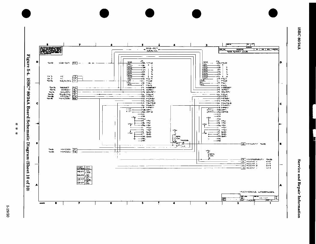
• ~ .... ~ ., (!)
en ~ ... 00 C:I (")
@
I)) 0 --~ ~ C:I 0
= ., ~ 00
* Ir * * a. ...
~
t:1 ... = ~ = e ,.-.. 00
=-(!) (!) ..... I-' 0 0 .... I-' 0 '-'
01 ~
~
• • • • _ , ., ..... • 1-- 1--~I l:00-ro"7 __ __ - ... __ _
.... -- 1i::Ij, ~ ~,~'- L_.....;'!£=c.::..;""""'::::::::E=."T.:.....:O:;: ... ;: ... =-_________ -i
» """q '-00-1.0' ~ ; J~ M]~; ~; J~ M]C1 X04 ~., 4 IOD.. 'V;. 4-X'Os:. '2..~ -:. IDc:" ~ ~
SI-I3 .0.2. ~R xoc.. "2,1 {p 'lOt. "2.,1 (,p
SH'3 A \ CP 'I.O" \q """0 ~ l:O~ Iq MDI
~~ I:JL)J~J""l. ~ ~ ~ ~~~ ::~ ~ ~~ ~"'1.. ., ~""t.. ... '-. ., M .... "2...
"5,",,~ R'i:!.'SE'T "K =s ~ 0:, MQE.'5>ET "51-1~ IOa.OI' 7i:: \Ii I~/ 1'So :toaJ:)1' ~~ ~/ a \"!.~I ~~/
~~ ~~~~J ~ i"o ~~~ U)~~ "5.A-\& MMc..c::..0/ ~ )'2.'2. MC.~01 '1..'1.. ~"S001'
-==. \"2.. MDoJ'T2 \ rl .. Mr.~'O:t. \ : \4 ~e 14 Mt.~Q.0
.----H---------->KP ~'\T/ I~ Mv.AI'T/ ,--=,-;----->~ MP"!!.."'/ eo ~'T/
E136 0-----------4"2.aOP'T\ ~'1&CO'T\ E137 ~'"!IO OPTCI'I ~~~0
~\O ...--410
4- -+CJ.J oQ,. ~ ~1 =t': +r ~: . - ~- ~ ~-~~:~~ t )~~~
-n.v ~n G\..E) I -1"1-V F§n G\..l.t:)
~!!h~ ~ ~~ _ ~'!n. ~ _ ~~
~~ ;;;~~ ~- l )~ ,::;~
- ~~ JOe. t44..'SJZ>e. - ~¥-
t 10 e c:.e. Mt"-"\~tT;' "'SJ.B
" U44
~e MMc~~/~rr~~~============~=========tt=t=======================================~~~~J
,
"=>'o-\e. MMC.s.."1..1 ~ .... :"~" ~ . Q'P'4-
a<:
W ;;:r~r~1 it:'C38 L-__ CJ~ I"t'IIDINT 2. SH~
CH ~ MIOINT (Z) Sl+~
~~. --L.f....§J Vo1l0INT \ 5~9
F0-F7 ~i"0 Fe-R= d~\ C0--Cl ~~ e,e-CF ~i,\
t--'il.JL\\l-"\()'D\.)\..E.\~o;;.
L -1- I'-~ 1-D I 147° 7'2 B __ ICM.£ ItUT 1 - - - _...... - - -
... rn = C":l
~ """ >
rn m ~ ... (') m
~ =-!:'
"C:S e!. ... .... 1:1 8' a ~ ... ~

•
•
•
•
•
•
•
•
•
•
A computer, no matter how sophisticated, can only
do what it is "told" to do. One "tells" the computer what
to do via a series of coded instructions referred to as a Pro
gram. The realm of the programmer is referred to as Soft
ware, in contrast to the Hardware that comprises the actual
computer equipment. A computer's software refers to all of
the programs that have been written for that computer.
When a computer is designed, the engineers provide
thH Central Processing Unit (CPU) with the ability to per
form a particular set of operations. The CPU is designed
such that a specific operation is performed when the CPU
control logic decodes a particular instruction. Consequently,
the operations that can be performed by a CPU define the
computer's Instruction Set.
Each computer instruction allows the programmer to
initiate the performance of a specific operation. All com
puter's implement certain arithmetic operations in their in
struction set, such as an instruction to add the contents of
two registers. Often logical operations (e.g., OR the con
tents of two registers) and register operate instructions (e.g.,
increment a register) are included in the instruction sel. A
computer's instruction set will also have instructions that
move data between registers, between a register and memory,
and between a register and an liD device. Most instruction
sets also provide Conditional Instructions. A conditional
instruction specifies an operation to be performed only if certain conditions have been met; for example, jump to a
particular instruction if the result of the last operation was
zero. Conditional instructions provide a program with a
decision-making capability.
By logically organizing a sequence of instructions into a coherent program, the programmer can "tell" the corT].
!;>uter to perform a very specific and useful function.
The computer, however, can only execute programs
whose instructions are in a binary coded form (i.e., series
of 1 's and O's), that is called Machine Code. Because it
would be extremely cumbersome to program in machine
code, programming languages have been developed. There
are programs available which convert the programming lan
guage instructions into machine code that can be inter
preted by the processor.
One type of programming language is Assembly lan
guage. A unique assembly language mnemonic is assigned to
each of the computer's instructions. The programmer can
write a program (called the Source Program) using these
mnemonics and certain operands; the source program is
then converted into machine instructions (called the Object
Code). Each assembly language instruction is converted into
one machine code instruction (1 or more bytes) by an
Assembler program. Assembly languages are usually ma-
* All Mnemonics Copyrighted If) Intel Corporation 1976, 1977
APPENDIX A SOSSA INSTRUCTION SET
chine dependent (Le., they are usually able to run on only
one type of computer).
THE 8085A INSTRUCTION SET
The B085A instruction set includes five different types
of instructions:
• Data Transfer Group - move data between registers
or between memory and registers
• Arithmetic Group - add, subtract, increment or
decrement data in registers or in memory
• logical Group - AND, OR, EXCLUSIVE-OR, compare, rotate or complement data in registers or in
memory
• Branch Group - conditional and unconditional jump instructions, subroutine call instructions and
return instructions
• Stack, 1/0 and Machine Control Group - includes liD instructions, as well as instructions for main
taining the stack and internal control flags.
Instruction and Data Formats:
Memory for the 80B5A is organized into B-bit quanti
ties, called Bytes. Each byte has a unique 16-bit binary
address corresponding to its sequential position in memory.
The 80B5A can directly address up to 65,536 bytes of mem
ory, which may consist of both read-only memory (ROM)
elements and random-access memory (RAM) elements (read/ write memory).
Data in the BOB5A is stored in the form of 8-bit binary integers:
DATA WORD
D7 I D6 I D5 I D4 I D3 I D2 I D1 I DO
MSB LSB
When a register or data word contains a binary num
ber, it is necessary to establish the order in which the bits
of the number are written. I n the Intel B085A, BIT 0 is re
ferred to as the least Significant Bit (lSB), and BIT 1 (of
an 8 bit number) is referred to as the Most Significant Bit
(MSB).
The BOB5A program instructions may be one, two or
three bytes in length. Multiple byte instructions must be
stored in successive memory locations; the address of the
first byte is always used as the address of the instructions.
The exact instruction format will depend on the particular
operation to be executed.
A-I
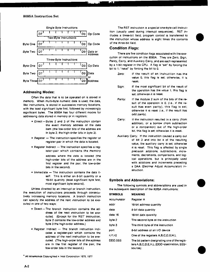
8085A Instruction Set
Single Byte Instructions
I D7 1 1 ~ I I 1 I DO lop Code Two- yte InstructIons
Byte One I D7 1 I 1 DO lop Code
Byte Two I D7 1 I DO I Data or Address
Three-Byte Instructions
Byte One ID7 1 I I I I I I DO lop Data
Byte Two ID7 1 I DO I/Data
Byte Thre~ D7 1 or
1 DO ~Address
Addressing Modes:
Often the data that is to be operated on is stored in memory. When multi-byte numeric data is used. the data. like instructions. is stored in successive memory locations, with the least significant byte first, followed by increasingly significant bytes. The 808SA has four different modes for addressing data stored in memory or in registers:
• Direct - Bytes 2 and 3 of the instruction contain the exact memory address of the data item (the low-order bits of the address are in byte 2. the high-order bits in byte 3).
• Register - The instruction specifies the register or register-pair in which the data is located.
• Register Indirect - The instruction specifies a register-pair which contains the memory
address where the data is located (the high-order bits of the address are in the first register and the paIr, the low-order bits in the second).
• Immediate - The instruction contains the data itself. This is either an 8-bit quantity or a 160bit quantity (least significant byte first, most significant byte second).
Unless directed by an interrupt or branch instruction, the execution of instructions proceeds through consecutively increasing memory locations. A branch instruction can specify the address of the next instruction to be executed In one of two ways:
• Direct - The branch instruction contains the address of the next instruction to be executed. (Except for the 'RST' instruction, byte 2 contains the low-order address and byte 3 the hIgh-order address.)
• Register Indirect - The branch instruction indicates a register-pair which contains the address of the next instruction to be executed. (The high-order bits of the address are in the first register of the pair, the low-order bits in the second.)
• All Mnemonics Copyrighted ~ Intel Corporation 1976. 1977
A-2
The RST instruction is a special one-byte call instruction (usually used during interrupt sequences). RST includes a three-bit field; program control i~ transferred to the instruction whose address is eight times the contents of the three-bit field.
Condition Flags: There are five condition flags associated with the exe
cution of instructions on the 808SA. They are Zero, Sign, Parity, Carry, and Auxiliary Carry, and are each represented by a 1-bit register in the CPU. A flag is "set" by forcing the bit to 1; "reset" by forcing the bit to O.
Zero: If the result of an instruction has the value 0, this flag is set; otherwise, it is reset.
Sign:
Parity:
Carry:
If the most significant bit of the result of the operation has the value 1, this flag is set; otherwise it is reset.
If the module 2 sum of the bits of the result of the operation is 0, (Le., if the result has even parity). this flag is set; otherwise it is reset (i.e., if the result has odd parity).
If the instruction resulted in a carry (from addition), or a borrow (from subtraction or a comparison) out of the high-order bit, this flag is set; otherwise it is reset.
Auxiliary Carry: If the instruction caused a carry out of bit 3 and into bit 4 of the resulting value, the auxiliary carry is set; otherwise it is reset. This flag is affected by single preciSion additions, subtractions. increments, decrements, comparisons, and logical operations, but is principally used with additions and increments preceding a DAA (Decimal Adjust Accumulator) tn-
struction.
Symbols and Abbreviations:
The following symbols and abbreviations are used in the subsequent description of the 808SA instructions:
SYMBOLS
accumulator
addr
data
data 16
byte 2
byte 3
port
r,r1,r2
DDD,SSS
MEANING
Register A
160bit address quantity
8-bit data quantity
160bit data quantity
The second byte of the instruction
The third byte of the instruction
8-bit address of an 1/0 device
One of the registers A,B,C,D,E,H,L
The bit pattern designating one of the registers A,B,C,D,E,H,L (DDD=destination, SSS= source):
•
•
•
•
•
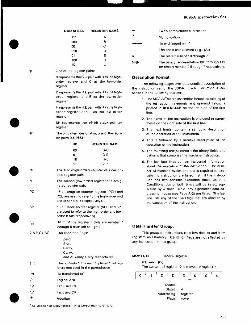
•
•
•
•
•
rp
RP
rh
rl
PC
SP
Z,S,P,CY,AC
( )
--1\
V \j
+
DDD orSSS REGISTER NAME
111 A
000 B
001 C 010 D 011 E
100 H 101 l
One of the register pairs:
B represents the B,C pair with B as the highorder register and C as the low-order register.
D represents the D,E pair with D as the highorder register and E as the low-order register.
H represents the H,l pair with H as the highorder register and l as the low-order register;
SP represents the 16-bit stack pOinter register.
The bit pattern designating one of the register pairs B,D,H,SP:
RP
00 01 10 11
REGISTER NAME
B-C D-E H-l
SP
The first (high-order) register of a designated reg ister pai r.
The second (low-order) register of a designated register pair.
16-bit program counter register (PCH and PCl are used to refer to the high-order and low-order 8 bits respectively).
16-bit stack pointer register (SPH and SPl are used to refer to the high-order and loworder 8 bits respectively).
Bit m of the register r (bits are number 7 through 0 from left to right).
The condition flags:
Zero, Sign, Parity, Carry, and Auxiliary Carry respectively.
The contents of the memory location of registers enclosed in the parentheses.
"Is transferred to"
logical AND
Exclusive OR
Inclusive OR
Addition
* All Mnemonics Copyrighted <J Intel Corporation 1976, 1977
*
n
NNN
8085A Instruction Set
Two's complement subtraction
Multiplication
"Is exchanged with"
The one's complement (e.g., (A))
The restart number 0 through 7
The binary representation 000 through 111 for restart number 0 through 7 respectively.
Description Format:
The following pages provide a detailed description of the instruction set of the 8085A. Each instruction is described in the following manner:
1. The MCS 85T"macro assembler format, consisting of the instruction mnemonic and operand fields, is printed in BOLDFACE on the left side of the first line.
2. The name of the instruction is enclosed in parenthesis on the right side of the first line.
3. The next line(s) contain a symbolic description of the operation of the instruction.
4. This is followed by a narative description of the operation of the instruction.
5. The following line(s) contain the binary fields and patterns that comprise the machine instruction.
6. The last four lines contain incidental information about the execution of the instruction. The number of machine cycles and states required to execute the instruction are listed first. If the instruction has two possible execution times. as in a Conditional Jump. both times will be listed, separated by a slash. Next, any significant data addressing modes (see Page A-2) are listed. The last line lists any of the five Flags that are affected by the execution of the instruction.
Data Transfer Group:
This group of instructions transfers data to and from registers and memory. Condition flags are not affected by any instruction in this group.
MOV r1, r2 (Move Register)
(r1) _ (r2)
The content of register r2 is moved to register r1.
o D I
D I
D I
S S S
Cycles: 1 States: 4
Addressing: register Flags: none
A-3

SOS5A Instruction Set
MOY r, M (Move from memory)
0
(r) ~ «H) (L)
The content of the memory location, whose address is in register Hand L, is moved to register r.
1 I
D I
D I
D 0
Cycles: 2 States: 7
Addressing: reg. indirect Flags: none
MOY M, r (Move to memory)
o
«H) (L» __ (r)
The content of register r is moved to the memory location whose address is in registers Hand L.
o
Cycles: 2 States: 7
Addressing: reg. indirect Flags: none
MYI r, data (Move Immediate) (r) _ (byte 2)
The content of byte 2 of the instruction is moved to register r.
o I o D D I D I 1 I 0
data
Cycles: 2 States: 7
Addressing: immediate Flags: none
MYI M, data (Move to memory immediate) «H) (L)) __ (byte 2)
The content of byte 2 of the instruction is moved to the memory location whose address is in registers H and L.
o I 0 I I 0 I 1 I 0
data
Cycles: 3 States: 10
Addressing: immed.!reg. indirect Flags: none
* All Mnemonics Copyrighted @ Intel Corporation 1976, 1977
A-4
LXI rp, data 16 (Load register pair immediate) (rh) __ (byte 3), (rl) _ (byte 2)
Byte 3 of the instruction is moved into the high-order register (rh) of the register pair rp. Byte 2 of the instruction is moved into the low-order register (rl) of the register pair rp.
o J o I R I
P I
0 I
low-order data
high-order data
Cycles: 3 States: 10
o I
Addressing: immediate Flags: none
0
LOA addr (Load Accumulator direct) (A) _ «byte 3) (byte 2»
I 1
The content of the memory location, whose address is specified in byte 2 and byte 3 of the instruction, is moved to register A.
o I o I 1 I 1 I 1
I
low-order addr
high-order addr
Cycles: 4 States:
Addressing: 13 direct none Flags:
o I
STA addr (Store Accumulator direct)
«byte 3) (byte 2)) --(A)
1 J
0
The content of the accumulator is moved to the memory location whose address is specified in byte 2 and byte 3 of the instruction.
o I o I 1 I
1 I 0 I o I 1 T 0
low-order addr
high-order addr
Cycles: 4 States: 13
Addressing: direct Flags: none
•
•
•
•
•

•
•
•
•
•
LHLD addr (Load Hand L direct)
(L) -- «byte 3) (byte 2)) (H) __ «byte 3) (byte 2) + 1)
The content of the memory location, whose address is specified in byte 2 and byte 3 of the instruction, is moved to register L. The content of the memory location at the succeeding address is moved to register H.
o I o 1 1 1
0 I
1 I
0 I
1 I
0
low-order addr
high-order addr
Cycles: 5 States: 16
Addressing: direct Flags: none
SHLD addr (Store Hand L direct)
0
(byte 3) (byte 2)) -- (L) «byte 3) (byte 2) + 1) --(H) The content of register L is moved to the memory location whose address is specified in byte 2 and byte 3. The content of register H is moved to the succeeding memory location.
I o I 1 I 0 I
0 1
0 I 1 I
0
low-order addr
high-order addr
Cycles: 5 States: 16
Addressing: direct Flags: none
LDAX rp (Load Accumulator indirect) (A)_«(rp)) The content of the memory location, whose address is in the register pair rp, is moved to register A. Note: Only register pairs rp=B (registers B and C) or rp=D (registers D and E) may be specified.
o I 0 I R P I 0 I o
Cycles: 2 States: 7
Addressing: reg. indirect Flags: none
* ,1\11 Mnemonics Copynghted ~, Intel Corporation 1976, 1977
BOB5A Instruction Set
STAX rp (Store Accumulator indirect)
o
«rp)) __ (A)
The content of register A is moved to the memory location whose address is in the register pair rp. Note: Only register pairs rp=B (registers Band C) or rp=D (registers D and E) may be specified.
o I R I P I 0
Cycles: 2 States: 7
I 0
Addressing: reg. indirect Flags: none
o
XCHG (Exchange Hand L with D and E) (H)----rD) (L) ___ (E)
The contents of registers Hand L. are exchanged with the contents of registers D and E.
I 0 I 0
Cycles: 1 States: 4
Addressing: register Flags: none
Arithmetic Group:
This group of instructions performs arithmetic operations on data in registers and memory.
Unless indicated otherwise, all instructions in this group affect the Zero, Sign, Parity, Carry, and Auxiliary Carry flags according to the standard rules.
All subtraction operations are performed via two's complement arithmetic and set the carry flag to one to indicate a borrow and clear it to indicate no borrow.
ADD r (Add register) (A) __ (A) + (r)
The content of register r is added to the content of the accumulator. The result is placed in the accumulator.
o I o I 0 I 0 I s
Cycles: States: 4
Addressing: register Z,S,P,CV,AC Flags:
I S I s
A-5

8085A Instruction Set
ADD M (Add memory) (A)_ (A) + ((H) (L))
The content of the memory location whose address is contained in the Hand L registers is added to the content of the accumulator. The result is placed in the accumulator.
0 I 0 0 0 0
Cycles: 2
States: 7 Addressing: reg. indirect
Flags: Z,S,P,CY,AC
ADI data (Add immediate) (A) _ (A) + (byte 2)
The content of the second byte of the instruction is added to the content of the accumulator. The result is placed in the accumulator.
o o I 0
data
Cycles: States:
Addressing: Flags:
2 7
immediate Z,S,P,CY,AC
o
ADC r (Add Register with carry) (A) _ (A) + (r) + (CY)
The content of register r and the content of the carry bit are added to the content of the accumulator. The result is placed in the accumulator.
o I o o
Cycles: States:
Addressing: Flags:
I S
1
4 register Z,S,P,CY,AC
S S
ADC M (Add memory with carry) (A)_ (A) + ((H) (L)) + (CY) The content of the memory location whose address is contained in the Hand L registers and the contents of the CY flag are added to the accumulator. The result is placed in the accumulator.
o I o I 0 I 1 I 1
Cycles: 2 States: 7
Addressing: reg. indirect Z,S,P,CY,AC Flags:
o
• All Mnemonics Copyrighted'" Intel Corporation 1976, 1977
A-6
ACI data (Add immediate with carry) (A) _ (A) + (byte 2) + (CY)
The content of the second byte of the instruction and the content of the CY flag are added to the contents of the accumulator. The result is placed in the accumulator.
o o
data
Cycles: States:
Addressing: Flags:
2 7 immediate Z,S,P,CY,AC
SUB r (Subtract Register) (A) _ (A) - (r)
o
The content of register r is subtracted from the content of the accumulator. The result is placed in the accumulator.
o I o
Cycles: States:
Addressing: Flags:
o S
4 register Z,S,P,CY,AC
SUB M (Subtract memory) (A) __ (A) - ((H) (L))
S S
The content of the memory location whose address is contained in the Hand L registers is subtracted from the content of the accumulator. The result is placed in the accumulator.
o I o o
Cycles: 2 States: 7
Addressing: reg. indirect Z,S,P,CY,AC Flags:
o
•
•
•
•
•

•
•
•
•
•
SUI data (Subtract immediate) (A) ___ (A) - (byte 2)
The content of the second byte of the instruction is subtracted 'from the content of the accumulator. The result is placed in the accumulator.
1 I o o
data
Cycles: States:
Addressing: Flags:
2 7 immediate Z,S,P,CY,AC
SBB r (Subtract Register with borrow) (A)_(A) - (r) - (CY)
o
The content of register r and the content of CY flag are both subtracted from the accumulator. The result is placed in the accumulator.
o I o I 1
Cycles: States:
Addressing: Flags:
I 1 I S
4 register Z,S,P,CY,AC
S
SBB M (Subtract memory with borrow) (A)_ (A) - ((H) (l)) - (CY)
S
The content of the memory location whose address is contained in the Hand l registers and the content of the CY flag are both subtracted from the accumulator. The result is placed in the accumulator.
o I o I 1
Cycles: 2 States: 7
I 1
Addressing: reg. indirect Z,S,P,CY,AC Flags:
* All Mnemoni'cs Copyrighted <, Intel Corporation 1976, 1977
o
8085A Instruction Set
SBI data (Subtract immediate with borrow) (A) - (A) - (byte 2) - (CY) The contents of the second byte of the instruction and the contents of the CY flag are both subtracted from the accumulator. The result is placed in the accumulator.
o
data
Cycles: States:
Addressing: Flags:
2 7 immediate Z,S,P,CY,AC
o
INR r (Increment Register)
0
(r)_ (r) + 1
The content of register r is incremented by one. Note: All condition flags except CY are affected.
0 I
D I D I D 0 I
0 I Cycles: States: 4
Addressing: register Flags: Z,S,P,AC
INR M (Increment memory) ((H) (l))_ ((H) (l)) + 1
The content of the memory location whose address is contained in the Hand l registers is incremented by one. Note: All condition flags except CY are affected.
o I 0 I o o 0] Cycles: 3 States: 10
Addressing: Flags:
reg. indirect Z,S,P,AC
DCR r (Decrement Register)
0
(r) __ (r) -1
The content of register r is decremented by one. N(lte: All condition flags except CY are affected.
I 0 I D
I D D 0
I
Cycles: States: 4
Addressing: register Flags: Z,S,P,AC
A-7
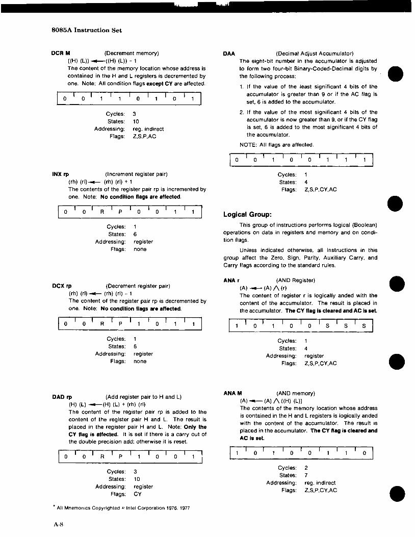
8085A Instruction Set
OCR M (Decrement memory)
0
((H) (L)) __ ((H) (L)) - 1
The content of the memory location whose address is contained in the Hand L registers is decremented by one. Note: All condition flags except CY are affected.
0 I I
0 I
1 0 I
1
Cycles: 3 States: 10
Addressing: reg. indirect Flags: Z,S,P,AC
INX rp (Increment register pair)
0
(rh) (rl) _ (rh) (rl) + 1
The contents of the register pair rp is incremented by one. Note: No condition Ilags are affected.
0 I
R I
P I
0 I
0 I I
1
Cycles: 1 States: 6
Addressing: register Flags: none
DCX rp (Decrement register pair)
o
(rh) (rl) _ (rh) (rl) - 1
The content of the register pair rp is decremented by one. Note: No condition flags are affected.
I 0 I R I P I 1 I 0 I
Cycles: 1 States: 6
Addressing: register Flags: none
DAD rp (Add register pair to Hand L)
o
(H) (L) _(H) (L) + (rh) (rl) The content of the register pair rp is added to the content of the register pair Hand L. The result is placed in the register pair Hand L. Note: Only the CY flag Is affected. It is set if there is a carry out of the double precision add; otherwise it is reset.
I 0 I R I P
Cycles: States:
Addressing: Flags:
I 1 I 0 I
3 10 register CY
o
* All Mnemonics Copyrighted ~) Intel Corporation 1976, 1977
A-8
DAA (Decimal Adjust Accumulator)
0
The eight-bit number in the accumulator is adjusted to form two four-bit Binary-Coded-Decimal digits by the following process:
1. If the value of the least significant 4 bits of the accumulator is greater than 9 or if the AC flag is set, 6 is added to the accumulator.
2. If the value of the most Significant 4 bits of the accumulator is now greater than 9, or if the CY flag is set, 6 is added to the most significant 4 bits of the accumulator.
NOTE: All flags are affected.
1 0
I I 0
I 0
Cycles: States: 4 Flags: Z,S,P,CY,AC
Logical Group:
This group of instructions performs logical (Boolean) operations on data in registers and memory and on condition flags.
Unless indicated otherwise, all instructions in this group affect the Zero, Sign, Parity, Auxiliary Carry, and Carry flags according to the standard rules.
ANA r (AND Register) (A) _ (A) /\ (r)
The content of register r is logically anded with the content of the accumulator. The result is placed in the accumulator. The CY Ilag Is cleared and AC Is set.
0 I I
0 I
0 I
S I
S I
S
Cycles: States: 4
Addressing: register Flags: Z,S,P,CY,AC
ANA M (AND memory) (A) __ (A) /\ ((H) (L))
The contents of the memory location whose address is contained in the Hand L registers is logically anded with the content of the accumulator. The result is placed in the accumulator. The CY Ilag Is cleared and AC is set.
0 I I
0 I
0 0
Cycles: 2 States: 7
Addressing: reg. indirect Flags: Z,S,P,CY,AC
•
•
•
•
•
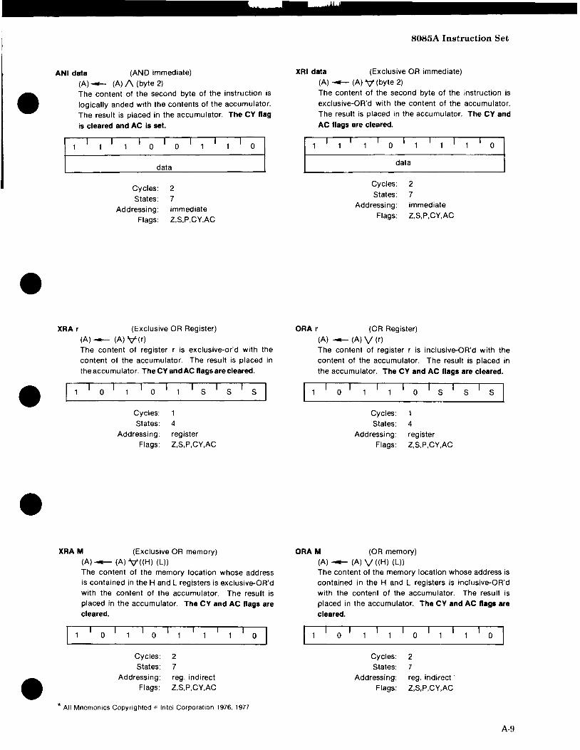
•
•
•
•
•
ANI data (AND immediate)
(A) -- (A) 1\ (byte 2) The content of the second byte of the instruction is logically anded with the contents of the accumulator. The result is placed in the accumulator. The CY flag Is cleared and AC is set. r: ______________ O ___ I __ O ___ 1 __ 1 _________ 0~
[ data
Cycles: States:
Addressing: Flags:
2 7 immediate Z,S,P,CY,AC
XRA r (Exclusive OR Register)
[1
(A)_ (A) "i"(r)
The content of register r is exclusive-or'd with the content of the accumulator. The result is placed in the accumulator. The CY andAC flags are cleared.
0 I I
0 I
S I
S I
S
Cycles: 1
States: 4 Addressing: register
Flags: Z,S,P,CY,AC
XRA M (Exclusive OR memory)
[
(A) __ (A) "V'((H) (L))
The content of the memory location whose address is contained in the Hand L registers is exclusive-OR'd with the content of the accumulator. The result is placed in the accumulator. The CY and AC flags are cleared.
o o
Cycles: 2 States: 7
Addressing: Flags:
reg. indirect Z,S,P,CY,AC
I 0
• All Mnemonics COPYrighted ~) Intel Corporation 1976. 1977
8085A Instruction Set
XRI data (Exclusive OR immediate)
(A) -- (A) '\1 (byte 2) The content of the second byte of the instruction is exclusive-OR'd with the content of the accumulator. The result is placed in the accumulator. The CY and AC flags are cleared.
o o
data
Cycles: 2 States: 7
Addressing: immediate Flags: Z,S,P,CY,AC
ORA r (OR Register) (A) __ (A) V (r)
The content of register r is inclusive-OR'd with the content of the accumulator. The result is placed in the accumulator. The CY and AC flags are cleared.
o I
Cycles: States:
Addressing: Flags:
o 50
1
4 register Z,S,P,CY,AC
ORA M (OR memory) (A) __ (A) V ((H) (L))
S S
The content of the memory location whose address is contained in the Hand L registers is inclusive-OR'd with the content of the accumulator. The result is placed in the accumulator. The CY and AC flags are cleared.
0 I I
0 0
Cycles: 2 States: 7
Addressing: reg. indirect Flags: Z,S,P,CY,AC
A-9

8085A Instruction Set
ORI data (OR immediate) (A) _ (A) V (byte 2)
The content of the second byte of the instruction is inclusive-OR'd with the content of the accumulator. The result is placed in the accumulator. The CY and AC flags are cleared.
1 I o
data
Cycles: 2 States:
Addressing: Flags:
7
immediate Z,S,P,CY,AC
o
CMPr (Compare Register) (A) - (r)
The content of register r is subtracted from the accumulator. The accumulator remains unchanged. The condition flags are set as a result of the subtraction. The Z flag is set to 1 if (A) = (r). The CY flag is set to 1 If (A)< (r).
o I S
Cycles: States: 4
Addressing: Flags:
register Z,S,P,CY,AC
S S
CMP M (Compare memory) (A) - «H) (L))
The content of the memory location whose address is contained in the Hand L registers is subtracted from the accumulator. The accumulator remains unchanged. The condition flags are set as a result of the subtraction. The Z flag Is set to 1 if (A) = «H) (L». The CY flag is set to 1 if (A)<((H) (L».
o I
Cycles: 2 States:
Addressing: Flags:
7
reg. indirect Z,S,P,CY,AC
* All Mnemonics Copyrighted © Intel Corporation 1976, 1977
A-IO
CPI data (Compare immediate)
RLC
RRC
(A) - (byte 2) The content of the second byte of the instruction is subtracted from the accumulator. The condition flags are set by the result of the subtraction. The Z flag is set to 1 if (A) = (byte 2). The CY flag is set to 1 if (A) «byte 2).
1 I
data
Cycles: States:
Addressing: Flags:
2 7 immediate Z,S,P,CY,AC
(Rotate left)
(An+1) --- (An); (AO) -- (A7) (CY)_(A7)
o
The content of the accumulator is rotated left one positi6n. The low-order bit and the CY flag are both set to the value shifted out of the high-order bit position. Only the CY flag Is affected_
o I 0 I o I o o
o
Cycles: States: Flags:
1 4 CY
(Rotate right)
(An) -- (An-1); (A7) ~ (AO) (CY)- (AO) The content of the accumulator is rotated right one position. The high-order bit and the CY flag are both set to the value shifted out of the low-order bit position. Only the CY flag is affected.
o I o I o
Cycles: States: Flags:
1
4 CY
•
•
•
•
•

•
•
•
•
•
RAL
RAR
(Rotate left through carry) (An+1)- (An); (CY)- (A7) (AO)--(CY) The content of the accumulator is rotated left one position through the CY flag. The low-order bit is set equal to the CY flag and the CY flag is set to the value shifted out of the high-order bit. Only the CY flag Is affected.
Cycles: 1
States: 4 Flags: CY
(Rotate right through carry)
(An) -- (An+l); (CY) - (Aol (A7)- (CY) The content of the accumulator is rotated right one position through the CY flag. The high-order bit is set to the CY flag and the CY flag is set to the value shifted out of the low-order bit. Only the CY flag is affected.
o I o o
Cycles: States: 4 Flags: CY
CMA (Complement accumulator) (A) __ (A)
The contents of the accumulator are complemented (zero bits become 1, one bits become 0). No flags are affected.
o I o o
Cycles: 1 States: 4 Flags: none
* All Mnemonics Copyrighted'" Intel Corporation 1976. 1977
CMC
o
STC
0
BOB5A Instruction Set
(Complement carry)
(CY) --- (CY) The CY flag is complemented. No other flags are affected.
o I I 1
(CY)-l
Cycles: 1 States: 4 Flags: CY
(Set carry)
The CY flag is set to 1. No other flags are affected.
I 0
I I 1 0 I 1
Cycles: States: 4 Flags: CY
Branch Group:
This group of instructions alter normal sequential program flow.
Condition flags are not affected by any instruction in this group.
The two types of branch instructions are unconditional and conditional. Unconditional transfers simply perform the specified operation on register PC (the program counter). Conditional transfers examine the status of one of the four processor flags to determine if the specified branch is to be executed. The conditions that may be specified are as follows:
CONDITION
NZ - not zero (Z = 0) Z - zero (Z = 1)
NC - no carry (CY = 0) C - carry (CY = 1)
PO - parity odd (P = 0) PE - parity even (P = 1)
P - plus (S = 0) M - minus (S = 1)
CCC
000 001 010 011 100 101 110 111
A-ll

8085A Instruction Set
JMP addr (Jump)
1
(PC)- (byte 3) (byte 2) Control is transferred to the instruction whose address is specified in byte 3 and byte 2 of the current instruction.
I 1
I 0
I 0
I 0
I 0
I 1
I 1
low-order addr
high-order addr
Cycles: 3 States: 10
Addressing: immediate Flags: none
Jcondltlon addr (Conditional jump)
1
If (CCC). (PC) - (byte 3) (byte 2)
If the specified condition is true. control is transferred to the instruction whose address is specified in byte 3 and byte 2 of the current instruction; otherwise. control continues sequentially.
I 1
I C
I C I C I
0 I
1 0
low-order addr
high-order addr
Cycles: 2/3 States: 7/10
Addressing: immediate Flags: none
CALL addr (Call) ((SP) -1)- (PCH) ((SP) - 2) -- (PCl) (SP) ---(SP) - 2 (PC) - (byte 3) (byte 2)
The high-order eight bits of the next instruction address are moved to the memory location whose address is one less than the content of register SP. The low-order eight bits of the next instruction address are moved to the memory location whose address is two less than the content of register SP. The content of register SP is decremented by 2. Control is transferred to the instruction whose address is specified in byte 3 and byte 2 of the current instruction.
* All Mnemonics Copyrighted © Intel Corporation 1976. 1977
A-12
1 I 1 I 0
I 0
I 1
I
low-order addr
high-order addr
Cycles: States:
5 18
1 I
0 I
1
Addressing: immediate/reg. indirect none Flags:
Ccondition addr (Condition call)
1
RET
If (CC). ((SP) -1) -- (PCH) ((SP) - 2) -- (PCl) (SP) - (SP) - 2 (PC) - (byte 3) (byte 2)
If the specified condition is true. the actions specified in the CAll instruction (see above) are performed; otherwise. control continues sequentially.
I 1
I C I C I C I
low-order addr
high-order addr
Cycles: 2/5 States: 9/18
1 I 0 I 0
Addressing: immediate/reg. indirect Flags: none
(Return) (PCl) __ ((SP»;
(PCH)-((SP) + 1); (SP) __ (SP) + 2;
The content of the memory location whose address is specified in register SP is moved to the low-order eight bits of register PC. The content of the memory location whose address is one more than the content of register SP is moved to the high-order eight bits of register PC. The content of register SP is incremented by 2.
1 I o I 0 I 0 o I 1
Cycles: 3 States: 10
Addressing: reg. indirect Flags: none
•
•
•
•
•
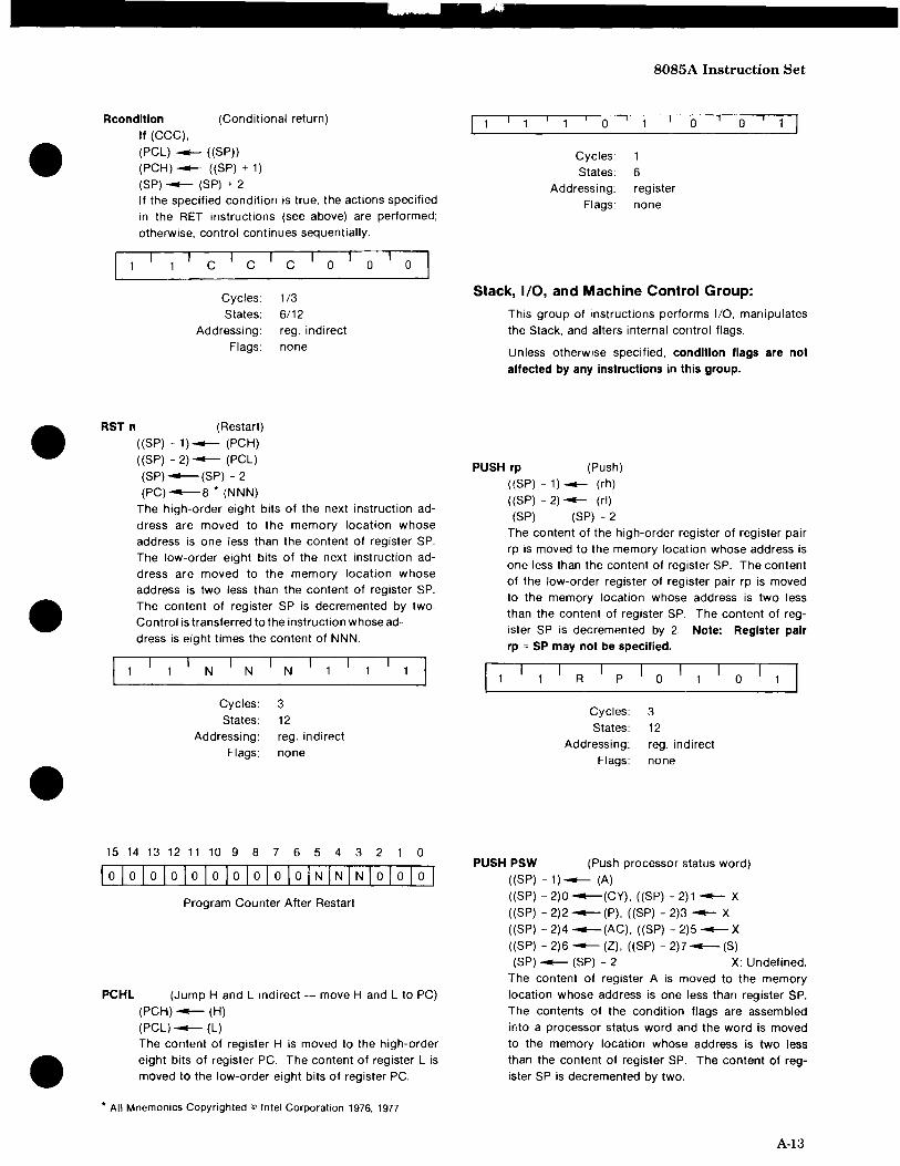
•
•
•
•
•
Rcondition (Conditional return)
If (CCC), (PCL) __ ((SP))
(PCH) -- ((SP) + 1) (SP) - (SP) + 2 If the specified condition is true, the actions specified in the RET instructions (see above) are performed; otherwise, control continues sequentially.
C I
C
Cycles: States:
Addressing: Flags:
RST n (Restart) ((SP) -1)_ (PCH)
((SP) - 2) -- (PCL)
(SP) --- (SP) - 2 (PC) ---8 * (NNN)
C I 0 0 0
1/3 6/12 reg. indirect none
The high-order eight bits of the next instruction ad
dress are moved to the memory location whose address is one less than the content of register SP. The low-order eight bits of the next instruction address are moved to the memory location whose address is two less than the content of register SP. The content of register SP is decremented by two. Control is transferred to the instruction whose address is eight times the content of NNN.
N I N I N
Cycles: 3 States: 12
Addressing: reg. indirect Flags: none
15 14 13 12 11 10 9 8 7 6 5 4 3 2 0
[ololololololololololNININlololo I Program Counter After Restart
PCHL (Jump Hand L indirect - move Hand L to PC) (PCH)-(H)
(PCL)- (L) The content of register H is moved to the high-order eight bits of register PC. The content of register L is moved to the low-order eight bits of register PC.
* All Mnemonics Copyrighted © Intel Corporation 1976, 1977
8085A Instruction Set
0 0 0
Cycles: 1
States: 6 Addressing: register
Flags: none
Stack, 110, and Machine Control Group:
This group of instructions performs liD, manipulates the Stack, and alters internal control flags.
Unless otherwise specified, condition flags are not affected by any instructions in this group.
PUSH rp (Push) ((SP) - 1) __ (rh)
((SP) - 2) -- (rl) (SP) (SP) - 2
The content of the high-order register of register pair rp is moved to the memory location whose address is one less than the content of register SP. The content of the low-order register of register pair rp is moved to the memory location whose address is two less than the content of register SP. The content of register SP is decremented by 2. Note: Register pair rp = SP may not be specified.
R I
P I 0 0
Cycles: 3 States: 12
Addressing: reg. indirect Flags: none
PUSH PSW (Push processor status word) ((SP) -1)_ (A)
((SP) - 2)O--(CY), ((SP) - 2)1-- X ((SP) - 2)2 -(P), ((SP) - 2)3 -- X ((SP) - 2)4 -(AC), ((SP) - <')5-X ((SP) -2)6-(Z), ((SP) -2)7---(S)
(SP) - (SP) - 2 X: Undefined, The content of register A is moved to the memory location whose address is one less than register SP. The contents of the condition flags are assembled into a processor status word and the word is moved to the memory location whose address is two less than the content of register SP. The content of register SP is decremented by two.
A-13

8085A Instruction Set
0 0
Cycles: 3 States: 12
Addressing: reg. indirect Flags: none
FLAG WORO
07 06 05 04 03 02 01 00
S Z X AC X P X CY I X: undefined
POP rp (Pop) (rl) _ ((SP)) (rh) ___ ((SP) + 1)
(SP) --- (SP) + 2 The content of the memory location, whose address is specified by the content of register SP, is moved to the low-order register of register pair rp. The content of the memory location, whose address is one more than the content of register SP, is moved to the highorder register of register pair rp. The content of register SP is incremented by 2. Note: Register pair rp = SP may not be specified.
1 I R I P o o o
Cycles: 3 States: 10
Addressing: reg. indirect Flags: none
POP PSW (Pop processor status word) (CY)- ((SP))O
(P) -- ((SP))2 (AC)- ((SP))4 (Z)- ((SP))6 (S) __ ((SP))7
(AP) -- ((SP) + 1) (SP) ~ (SP) + 2 The content of the memory location whose address is specified by the content of register SP is used to restore the condition flags. The content of the memory location whose address is one more than the content of register SP is moved to register A. The content of register SP is incremented by 2.
o I 0 o
Cycles: 3 States: 10
Addressing: reg. indirect Flags: Z,S,P,CY,AC
* All Mnemonics Copyrighted © Intel Corporation 1976, 1977
A·14
XTHL (Exchange stack top with Hand L) (L)---((SP)) (H)---((SP) + 1) The content of the L register is exchanged with the content of the memory location whose address is specified by the content of register SP. The content of the H register is exchanged with the content of the memory location whose address is one more than the content of register SP.
Cycles: 5 States: 16
Addressing: reg. indirect Flags: none
SPHL (Move HL to SP) (SP)-- (H) (L)
The contents of registers Hand L (16 bits) are moved to register SP.
Cycles: 1
States: 6 Addressing: register
Flags: none
IN port (Input) (A)_ (data) The data placed on the eight bit bi-directional data bus by the specified port is moved to register A.
o I 1 I 1 I 0
port
Cycles: 3 States: 10
Addressing: direct Flags: none
OUT port (Output) (data) __ (A)
The content of register A is placed on the eight bit bi-directional data bus for transmission to the specified port.
o I 1 I 0 I 0 I 1 I 1
port
Cycles: 3 States: 10
Addressing: direct Flags: none
•
•
•
•
•
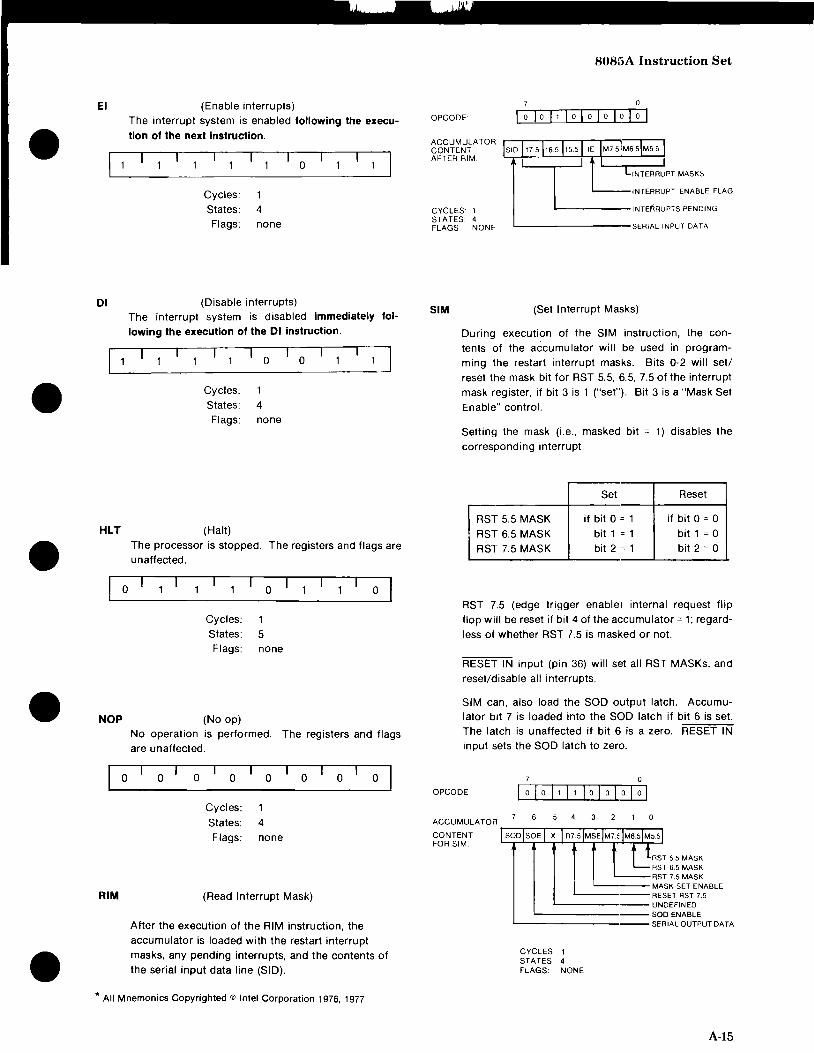
•
•
•
•
EI
01
(Enable interrupts) The interrupt system is enabled following the execu
tion of the next Instruction.
I 1 I 0
Cycles: 1
States: 4 Flags: none
(Disable interrupts) The interrupt system is disabled immediately following the execution of the 01 instruction.
L----_____ ]
HLT
0
(Halt)
The processor is stopped. The registers and flags are unaffected.
0 0
Cycles: 1 States: 5 Flags: none
NOP (No op)
o
RIM
No operation is performed. The registers and flags are unaffected.
o I o o o o o I o
Cycles:
States: 4 Flags: none
(Read Interrupt Mask)
After the execution of the RIM instruction, the accumulator is loaded with the restart interrupt
masks, any pending interrupts, and the contents of the serial input data line (SID).
* All Mnemonics Copyrighted © Intel Corporation 1976, 1977
OPCODE:
ACCUMULATOR CONTENT AFTER RIM:
CYCLES: 1 STATES: 4 FLAGS NONE
8085A Instruction Set
7 0
10 10 11 101010 lolal
INTERRUPT ENABLE FLAG
L.------INTE!\RUPTS PENDING
'----------SERIAL INPUT DATA
SIM (Set Interrupt Masks)
During execution of the SIM instruction, the con
tents of the accumulator will be used in programming the restart interrupt masks. Bits 0-2 will set! reset the mask bit for RST 5.5, 6.5, 7.5 of the interrupt
mask register, if bit 3 is 1 ("set"). Bit 3 is a "Mask Set
Enable" control.
Setting the mask (i.e., masked bit = 1) disables the
corresponding interrupt.
Set Reset
RST 5.5 MASK if bit 0 = 1 if bit 0 = 0
RST 6.5 MASK bit 1 = 1 bit 1 = 0
RST 7.5 MASK bit 2 = 1 bit 2 = 0
RST 7.5 (edge trigger enable) internal request flip flop will be reset if bit 4 of the accumulator = 1; regard
less of whether RST 7.5 is masked or not.
RESET IN input (pin 36) will set all RST MASKs, and
reset/disable all interrupts.
SIM can, also load the SOD output latch. Accumulator bit 7 is loaded into the SOD latch if bit 6 is set. The latch is unaffected if bit 6 is a zero. RESET IN input sets the SOD latch to zero.
7 a OPCODE lolal111lolal~
ACCUMULATOFl a
CONTENT r-~-~-r-~-r--r--r~
FOR SIM:
'------RESET RST 7.5 '--------- UNDEFINED
1..-------- SOD ENABLE '------------SERIAL OUTPUT DATA
CYCLES' 1 STATES: 4 FLAGS: NONE
A-15

8085A Instruction Set
INSTRUCTION SET
Summary of Processor Instructions
Inslruction Code [1) Clock[2) Instruction Code [1) Clock [2) Mnemonic Description 07 06 OS 04 03 02 01 DO Cycles Mnemonic Description 07 06 OS 04 03 D2 01 DO Cycles
MOV r1, r2 Move register to register
MOV M. r Move register to memory MOV r, M Move memory to register HLT Halt MVI r Move immediate register MVI M Move immediate memory INR r Increment register DCR, INR M OCR M ADD, ADC, SUB, SBB,
ANA, XRA, ORA, CMP, ADD m
AOCM SUB M SBB M
ANA M XRA M
ORAM CMPM ADI ACI
SUI SBI
ANI XRI
ORI CPI RLC RRC RAL RAR
JMP JC JNC JZ JNZ JP JM JPE JPO CALL CC CNC CZ CNZ CP CM CPE CPO RET RC RNC
Decrement register Increment memory Decrement memory
Add register to A Add register to A with carry Subtract register from A Subtract register from A
with borrow And register with A
Exclusive Or register with A Or register with A Compare register with A Add memory to A Add memory to A with carry Subtract memory from A Subtract memory from A
with borrow
And memory with A Exclusive Or memory with A
Or memory with A Compare memory with A Add immediate to A
Add immediate to A with carry
Subtract Immediate from A
Subtract immediate from A with borrow And immediate with A Exclusive Or Immediate with A Or immediate with A
Compare immediate with A
Rotate A left Rotate A right
Rotate A left through carry Rotate A right through carry Jump unconditional Jump on carry
Jump on no carry Jump on zero Jump on no zero Jump on positive
Jump on Minus Jump on parity even Jump on parity odd
Call unconditional Callan carry Calion no carry Call on zero Call on no zero Call on positive Call on minus Calion panty even
Gall on panty odd Return Return on carry Return on na carry
DOOSSS lIS S S
ODD 0 1 1 0
ODD 0 0 o 0 1 1 0
o 0 D D D
o D D 0
o 1 0
o 0
o 0 o o
o o o
o
1
o
000 000 o
o 1
010 o 0 o
1
1
o
o 0
o 1
o 0
1
1 0
1 0 o 0
o 1
o 1 0 1
S S S S 5 S S S S S S S
S S S S S S S S S S S S
o o
1
o 0 o 0
o
o o o
t o 0
o 0 o o o 0
o o 0
100 o 0 o 0
10
5
10 10
4
4
4
4
10 10 10 to to 10 10
10 10 17
11/17 11/17
11/17 11/17 11/17 11/17 11/17
11/17
10 51tt 5/11
RZ RNZ RP RM RPE RPO RST IN OUT LXI B
LXI 0
LXI H
LXI SP PUSH B
PUSH D
PUSH H
Return on zero
Return on no zero Return an positive Return on minus Return on parity even Return on parity odd
Restart Input Output Load Immediate register
Palf B & C Load Immediate register Pai, 0 & E Load immediate register 0 Pal( H & L Load Immediate stack pointer 0
Push register Pair B & C on stack Push register Pair 0 & E on
stack Push register Pair H & L on
stack PUSH PSW Push A and Flags
POP B
POP 0
POP H
on stack Pop register pair 8 & C off stack Pop register pair D & E off stack
Pop register pair H & L off stack
o
1 0 I 0
1
o o
A A A 1
1
o
1
o
o
o
o 0
o o 0 o 0
o o
o
1
o
POP PSW Pop A and Flags off stack 1 1 o 0 ST A Store A direct o 0 o 0 LDA XCHG
Load A direct 0 0 1
o
XTHL SPHL PCHL DAD B DAD 0 DAD H DADSP STAX B STAX D LDAX B LOAX 0 INX B INXD INXH INX SP DCX B DCX 0 DCX H DCX SP CMA STC CMC DAA SHLD LHLD EI
DI NOP RIM SIM
Exchange 0 & E, H & L Registers
Exchange top of stack. H & L H & L to stack painter H & L to program counter Add B & C to H & L Add D & E to H & L Add H & L to H & L Add stack pointer to H & L Store A indirect Store A indirect Load A indirect
Load A Indirect
Increment B & C registers Increment D & E registers Increment H & L registers Increment stack pointer
Decrement B & C Decrement 0 & E Decrement H & L
Decrement stack pointer Complement A
Set carry Complement carry Decimal adjust A
Store H & L direct Load H & L direct Enable Interrupts Disable Interrupts
No-operation Read Interrupt Mask Set I nterrupt Mask
o
ttl 0
o 0 0 0 o 0 1 o 0
o 0 1 t
o 0 0 0 o 0 0
o o
o
o 0 o o
o 0 0
000 o 0 o 0 o 0 o 0 o o 0 o 0 o 1 1 1 1
o 0 o 0 a
o 1
o
o 1
o 1 o
1
o a o
1
o o
1 o o
I
o o
o
o 0
o 0 o o
o
o o o
o
o o o o
o 0
NOTES: 1. DDD or SSS - 0008 - 001 C - 010 D - 011 E -100 H -101 L -110 Memory - 111 A. 2, Two possible cycle times, (5/11) indicate instruction cycles dependent on condition flags.
* * * A-16
o o
1
o o
o o
o
1
1
o o
5/tl 5/11 5/tl 5/11
5/t 1 5/tt 11 to 10 10
10
10
10 lt
11
tl
11
to
10
10
10 13
13 4
18 5
to 10 to 10
4
4 4 t6 16 4
•
•
•
•
•

•
•
•
•
•
8-1. INTRODUCTION
The iSBC SO/24A board utilizes a factory programmed decode PROM to produce certain memory and 110 related signals. The PROM (device U32) is shown in figure 5-4, sheet S. This appendix provides a brief description of the decode PROM, including a me,mory map.
8-2. DESCRIPTION
An Intel 3625A-1 PROM (lK x 4) is used for this application. It is programmed at the factory, as shown in table B-l. There are ten active inputs and four active outputs, as outlined below:
INPUTS
Addresses AA-AF - From the 80S5A-2.
MMPRESENT I - Indicates that I/O addresses CO-CF and FO-FF are valid, on-board I/O addresses.
PTYPE 0 & PTYPE 1
IOI
SIGNAL
AA-AF
PTYPE 0-1
IOI MMPRESENTI
DCDPROM 1 & DCDPROM 2
- Indicate whether 1K, 2K, 4K or SK PROMs are being utilized for on-board program storage.
- Indicates an I/O cycle when true. However, when 101 is false, a memory access cycle is indicated.
DECODE PROM INPUT
AO-A5
A6-A7
AS
A9
OUTPUTS
- These signals (01 & 02) are used in two ways depending on the state of the 101 input.
APPENDIXB DECODE PROM (U32)
PROMACKI
ONBDIO
OUTPUT 4
MMPRESENTI
X
X
X
X
X = Irrelevant
MMPRESENTI
1
0
X = Irrelevant
101
1
1
1
1
When the 101 input is false, the two signals (DCDPROM 1 & DCDPROM 2) are decoded to select one out of four PROMs. When the 101 is true, the two signals (DCDPROM 1 & DCD PROM 2), in conjunction with another PROM output (03), are decoded to select on-board I/O devices.
- Enables the on-board PROM chip selects .
- Indicates that an I/O access is on-board.
- Is included in both PROM ACKI and ONBDIO and is considered a "valid access" bit.
On-Board PTYPE PTYPE Address PROM
0 1 Space Size (Hex)
0 0 OOOO-OFFF 1K
1 0 0OOO-1FFF 2K
0 1 0OOO-3FFF 4K
1 1 0OOO-7FFF 8K
101 PTYPE PTYPE On-Board 1/0 0 1 Address Space
0 X X D4-EF
0 X X CO-CF, D4-FF
B-1

AppendixB iSBC80/24A
Table B·I. Decode PROM Map • PRO" ADDRESS 0 1 2 3 " 5 6 7 8 9 A B C D E F
OO~ F F F F F F F F F F F F F F F F o l'-Qi F F F F F F F F F F F F F F F F 020 F F F F F F F F F F F F F F F F 030 3 3 3 3 F 6 0 4 F 1 2 5 3 3 3 3 040 F F F F F F F F F F F F F F F F 050 F F F F F F F F F F F F F F F F 060 F F F F F F F F F F F F F F F F 070 3 3 3 3 F 6 0 " F 1 2 5 3 J 3 J OBO F F F F F F F F F F F F F F F F 090 F F F F F F F F F F F F F F F F OAO F F F F F F F F F F F F F F F F OBO 3 3 3 3 F 6 0 4 F 1 2 5 3 3 3 3 OCO F F F F F F F F F F F F F F F F ODO F F F F F F F F F F F F F F F F OEO F F F F F F F F F F F F F F F F OFO 3 3 3 3 F 6 0 " F 1 2 5 3 3 3 3 100 " 5 6 7 F F F F F F F F F F F F 110 F F F F F F F F F F F F F F F F 120 F F F F F F F F F F F F F F F F • 130 F F F F F F F F F F F F F F F F 140 " " 5 5 6 6 7 7 F F F F F F F F 150 F F F F F F F F F F F F F F F F 160 F F F F F F F F F F F F F F F F 170 F F F F F F F F F F F F F F F F 180 4 4 " " 5 5 5 5 {, 6 , {, 7 7 7 7 190 F F F F F F F F F F F F F F F F lAO F F F F F F F F F F F F F F F F 180 F F F F F F F F F F F F F F F F leo 4 4 " " 4 4 " " 5 5 5 5 5 5 5 5 11>0 {, 6 6 {, 6 6 6 6 7 7 7 7 7 7 7 7 lEO F F F F F F F F F F F F F F F F IFO F F F F F F F F F F F F F F F F • 200 F F F F F F F F F F F F F F F F 210 F F F F F F F F F F F F F F F F 220 F F F F F F F F F F F F F F F F 230 F F F F F 6 0 4 F 1 2 5 F F F F 240 F F F F F F F F F F F F F F F F 250 F F F F F F F F F F F F F F F F 260 F F F F F F F F F F F F F F F F 270 F F F F F Ii 0 " F 1 2 5 F F F F 280 F F F F F F F F F F F F F F F F 290 F F F F F F F F F F F F F F F F 2AO F F F F F F F F F F F F F F F F 280 F F F F F 6 0 " F 1 2 5 F F F F 2CO F F F F F F F F F F F F F F F F • 21>0 F F F F F F F F F F F F F F F F 2E 0 F F F F F F F F F F F F F F F F 2F 0 F F F F F 6 0 4 F 1 2 5 F F F F 300 " 5 {, 7 F F F F F F F F F F F F 310 F F F F F F F F F F F F F F F F 320 F F F F F F F F F F F F F F F F 330 F F F F F F F F F F F F F F F F 340 " " 5 5 Ii 6 7 7 F F F F F F F F 350 F F F F F F F F F F F F F F F F 360 F F F F F F F F F F F F F F F F 370 F F F F F F F F F F F F F F F F 380 " 4 " " 5 5 5 5 Ii 6 6 Ii 7 7 7 7 390 F F F F F F F F F F F F F F F F 3AO F F F F F F F F F F F F F F F F 380 F F F F F F F F F F F F F F F F 3eo 4 4 " 4 4 4 4 4 5 5 5 5 5 5 5 5 3(>0 6 6 6 6 6 6 6 6 7 7 7 7 7 7 7 7 3EO F F F F F F F F F F F F F F F F 3F 0 F F F F F F F F F F F F F F F F
• * * * B-2
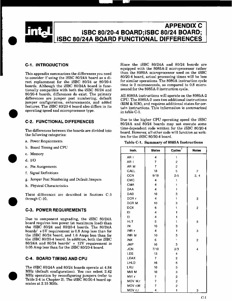
•
•
•
•
•
APPENDIX C iSBC 80/20-4 BOARD;iSBC 80/24 BOARD;
iSBC 80/24A BOARD FUNCTIONAL DIFFERENCES
C-1. INTRODUCTION
This appendix summarizes the differences you need to consider if using the iSBC SO/24A board as a direct replacement for the iSBC SO/24 or S0/20-4 boards. Although the iSBC SO/24A board is functionally compatible with both the iSBC SO/24 and S0/20-4 boards, differences do exist. The primary differences are jumper post numbering, default jumper configuration, enhancements, and added features. The iSBC S0/20-4 board also differs in its operating speed and microprocessor type.
C-,2. FUNCTIONAL DIFFERENCES
The differences between the boards are divided into the following categories:
a. Power Requirements
b. Board Timing and CPU
c. Memory
d. 1/0
e. Pin Assignments
f. Signal Definitions
g. Jumper Post Numbering and Default Jumpers
h. Physical Characteristics
These differences are described in Sections C-3 through C-lO.
C-3. POWER REQUIREMENTS
Due to component upgrading, the iSBC SO/24A board requires less power (at maximum load) than the iSBC SO/24 and S0/20-4 boards. The SO/24A boards' + 5V requirement is O.S Amp less than for the iSBC SO/24 board, and 1.6 Amps less than for the iSBC S0/20-4 board. In addition, both the iSBC SO/24A and 80/24 boards' + 12V requirement is 0.05 Amp less than for the iSBC S0/20-4 board.
C-4. BOARD TIMING AND CPU
The iSBC 80/24A and 80/24 boards operate at 4.S4 MHz (default configuration). You can select 2.42 MHz operation by reconfiguring jumpers (refer to Table 2-4 in Chapter 2). The iSBC S0/20-4 board operates at 2.15 MHz.
Since the iSBC SO/24A and SO/24 boards are equipped with the S085A-2 microprocessor rather than the SOSOA microprocessor used on the iSBC S0/20-4 board, actual processing times will be less for similar operations. The 8080A instruction cycle time is 2 microseconds, as compared to O.S microsecond for the S085A-2 instruction cycle.
All SOSOA instructions will operate on the SOS5A-2 CPU. The SOS5A-2 uses two additional instructions (RIM & SIM), and requires additional states for certain instructions. This information is summarized in table C-1.
Due to the higher CPU operating speed the iSBC SO/24A and SO/24 boards may not execute some time-dependent code written for the iSBC S0/20-4 board. However, all other code will function as written for the iSBC 80/20-4 board.
Table C-l. Summary of SOS5A Instructions
Instr. States Cycles 1
Notes
AR r 4 1
AR I 7 2
AR M 7 'I .. CALL 18 <.
,I 2 CCN 9/18 2/5 2,4
CMC 4 1
CMA 4 1
DAA 4 1
DAD 10 3
DCR r 4 1 3 DCR M 10 a DCX 6 1 2 DI 4 11
EI 4 1
HLT 5 1 5 IN 10 3
INR r 4 1 3 INR M 10 3 INX 6 11 2 JMP 10 " JCN 7110 2/3 4 LDS 13 4
LDAX 7 2 LHLD 16 5
LXU 10 3 MVI M 10 3 MVI r 7 2
MOV M,r 7 .) .-MOV r,M 7 2
MOV r,r 4 1 3
C-l

Appendix C
Table C-l. Summary of S085A Instructions (Continued)
Instr. States Cycles 1
NOP 4 1
OUT 10 3
PCHL 6 1
POP 10 3
PUSH 12 3
ROT 4 1
RET 10 3
RCN 6/12 1/3
RIM1 4 1
RST 12 3
SHLD 16 5
SIM1 4 1
STA 13 4
STAX 7 2
STC 4 1
XCHG 4 1
XTHL 16 5
SPHL 6 1
1 New Instruction
NOTES:
Notes
2
2
2
2
2
1. Two possible state-cycle times indicates dependence on condition flag.
2. Increase in states over 8080 due to necessity of a T 6
during M1.
3. Decreased from 5 to 4 states during M1.
4. Instruction branches over last address fetch if condi-tion false.
5. 5 cycles to get a HL T state. 1 cycle necessary to get out a HLT.
The 8085A-2 CPU has four interrupt inputs in addition to the INTR input. These inputs are accessed through the interrupt matrix, via jumper connection (refer to table 2-7 in text).
C-s. MEMORY
The iSBC 80/24A and 80/24 boards offer more onboard ROM (up to 32K bytes) and RAM (up to 8K bytes) than the iSBC 80/20-4 board. In certain configurations, ROM and RAM addressing may overlap. Chapter 2 provides instructions for proper memory configurations and addressing.
All ROM/PROM/EPROM devices used on the former boards may also be used on the iSBC 80/24A board. Chapter 2 provides installation instructions.
However, the RAM devices used on the iSBC 80124 board are not compatible with the iSBC 80124A and 80120-4 boards.
C-2
iSBC80/24A
0-6. 1/0 FACILITIES
All I/O capabilities and addressing are identical among the three boards. However, the iSBC 80/24A and 80/24 boards have additional I/O capability through the two iSBX Bus connectors (J5 and J6). If Multimodule boards are present, they require the following addressing):
J5
Ports CO-C7 for MCSOI
Ports C8-CF for MCSl/
J6
Ports FO-F7 for MCSO
Ports F8-FF for MCSl/
If Multimodule boards are not present, these addresses may be used for other applications.
C-7. PIN ASSIGNMENTS
•
Table C-2 provides pin assignment differences • among the three boards and the Multibus interface.
Table C-2. Pin Assignments
Pln# 80/24A, 80/24 80/20-4 Multlbus
P1-25 Reserved 1 AACKl RESERVED
P1-28 ADDRESS 10 RESERVED ADDRESS 10
P1-29 CBROI RESERVED CBROI
P1-33 RESERVED1 INTRI INTAI
P2-13 PFSRI RESERVED PFSRI
P2-19 PFINI PFII PFINI
P2-21,22 GRD RESERVED GRD
P2-30 RESERVED WAITI WAITI
P2-32 RESERVED1 BTMO RESERVED
P2-36 RESERVED1 INTAI RESERVED
P2-38 AUX RESETI RESETI AUXRESETI
J1-50 EXTERNAL
INTOR NOT USED N/A
J2-50 +5 VOLTS
1 Reserved in accordance with Multibus interface
specification.
C-s. SIGNAL DEFINITIONS
The signals BCLKI and CCLKI are approximately 108 0 out of phase with each other, and the new cycle period is reduced from 108.5 nsec to 103.3 nsec.
There is no WAIT/ signal provided on the iSBC 80/24A and 80/24 boards. For front panel (iSBC 655 Chassis) use, the signal ALE, P2-32, should be used for the RUN indicator. This is the standard front panel use for the RUN indicator and does not require any other wiring.
•
•
•

•
•
•
•
•
iSBC80/24A
INTA is supported only to the extent of being compatible with the iSBC 80/2-4 board. Because the iSBC 80/24A and 80/24 boards do not support bus vectored interrupts, INTA is not provided on PI.
C-9. JUMPER POST NUMBERING AND DEFAULT JUMPERS
There is no correlation between the jumper posts used on former boards and those used on the iSBC 80/24A board. In the factory default mode, the boards are jumpered for the same functions. These jumper connections are compared in table C-3.
AppendixC
'Ib alter a particular factory configuration jumper, refer to Chapter 2.
C-10. PHYSICAL CHARACTERISTICS
All connector locations on the iSBC 80/24A and 80/24 boards comply with the Multibus Interface Specification.
In addition, the two iSBX Bus connectors (J5 and J6) require consideration for component heights and connector locations.
Table C-3. Jumper Pairs
ISBC isac isac Isac 80/24A 80/24 80/20-4 80/24A Sheet Function Text
Jumper Pair Jumper Pair Jumper Pair Grid Reference Ref.
1-2 1-2 None 5-B2 Connects + 5 volts to J 1-50 None
3-4* 26-27* 52-53* 5-C4 Configures port E4 bus transceiver to output mode 2-24
4-18 27-41 51-52 5-C4 Configures port E4 bus transceiver to input mode 2-14
5-19* 28-42* 62-63* 5-C4 Connects port E6, bit 0 to driver/terminator socket 2-14
6-20* 29-43* 64-65* 5-C4 Connects port E6, bit 1 to driver/terminator socket 2-14
7-21 * 30-44* 66-67* 5-C4 Connects port E6, bit 2 to driver/terminator socket 2-14
8-22* 31-45* 68-69* 5-C4 Connects port E6, bit 3 to driver/terminator socket 2-14
9-24* 32-47* 60-61 * 5-C4 Connects port E6, bit 4 to driver/terminator socket 2-14
10-25* 33-48* 58-59* 5-C4 Connects port E6, bit 5 to driver/terminator socket 2-14 11-26* 34-49* 56-57* 5-C4 Connects port E6, bit 6 to driver/terminator socket 2-14 12-27* 35-50* 54-55* 5-C4 Connects port E6, bit 7 to driver/terminator socket 2-14 13-28* 36-51 * 93-94 * 5-C4 Applies + 5 volts to timer gate 0 (ITGO) None 14-29* 37-51 * 94-95* 5-C4 Applies + 5 volts to timer gate 1 (ITG1) None 15-30 38-52 None 5-C4 Connects timer 1 output to timer input matrix 2-11 15-XX 38-XX None 5-C4 Connects selected J1 bit to timer input matrix 2-11 16-XX 39-XX None 5-C4 Connects INTROUT/BANKSEL to selected E6 bit 2-11 17-19 40-42* hardwired 5-C4 Connects port E6, bit 0 to PIA 1 2-14 22-23 45-46* hardwired 5-C4 Connects port E6, bit 3 to PIB1 2-14 31-XX 53-XX None 5-C4 Connects PFSR/ to selected E6 bit 2-22 32-XX 54-XX None 5-C4 Connects PROM ENABLE to selected E6 bit 2-11 33-48 3-4 None 6-B2 Connects + 5 volts to J2-50 None 34-35* 55-56* 71-72* 6-C4 Configures port E8 bus transceiver to output mode 2-14 35-50 56-70 70-71 6-C4 Configures port E8 bus transceiver to input mode 2-14 36-51 * 57-71 * 81-82* 6-C4 Connects port EA, bit 0 to driver/terminator socket 2-14 37-52* 58-72* 83-84 * 6-C4 Connects port EA, bit 1 to driver/terminator socket 2-14 38-53* 59-73* 85-86* 6-C4 Connects port EA, bit 2 to driver/terminator socket 2-14 39-54* 60-74* 87-88* 6-C4 Connects port EA, bit 3 to driver/terminator socket 2-14 40-XX 61-XX 72-XX 6-C4 Ground post 2-14 41-56* 62-76* 79-80* 6-C4 Connects port EA, bit 4 to driver/terminator socket 2-14 42-57* 63-77· 77-78* 6-C4 Connects port EA, bit 5 to driver/terminator socket 2-14 43-58* 64-78* 75-76* 6-C4 Connects port EA, bit 6 to driver/terminator socket 2-14 44-59* 65-79* 73-74* 6-C4 Connects port EA, bit 7 to driver/terminator socket 2-14 45-XX 66-XX 97-XX 6-C4 Connects BOET/ to selected EA bit 2-14 46-XX 67-XX 96-XX 6-C4 Connects BRI/ to selected EA bit 2-14 47-XX 68-XX 90-XX 6-C4 Connects AUXO/ to selected EA bit 2-14
C-3

AppendixC iSBC80/24A
Table C-3. Jumper Pairs (Continued)
Isac Isac Isac Isac 80/24A 80/24 80/20-4 80/24A Sheet Function Text
Jumper Pair Jumper Pair Jumper Pair Grid Reference Ref. • 49-51 69-71 * hardwired 6-C4 Connects port EA, bit 0 to PIA21 2-14 54-55 74-75* hardwired 6-C4 Connects port EA, bit 3 to PIA 11 2-14 6O-XX 80-XX None 6-C4 Connects SOD to selected EA bit 2-14 61-XX 81-XX None 6-C4 Connects SID to selected EA bit 2-14 62-XX 82-XX 89-XX 6-C4 Connects AUX11 to selected EA bit 2-14 63-64* J4-1-J4-14 * hardwired 7-C3 Connects transmit data to J3-4 2-13 63-74 J4 None 7-C3 J3 serial jumper matrix 2-13 65-66* J4-2-J4-13 * hardwired 7-C3 Connects receive data to J3-6 2-13 67-68* J4-3-J4-12 * hardwired 7-C3 Connects RTS to J3-8 2-13 69-70* J4-4-J4-11 * hardwired 7-C3 Connects CTS to J3-10 2-13 71-72* J4-5-J4-1 0 * hardwired 7-C3 Connects OTR to J3-13 2-13 73-74* J4-6-J4-9* hardwired 7-C3 Connects -12 volts to J3-19 2-13 75-80 9-10 9-10 7-A2 Connects -12 volts to J3-19 2-25 76-77 5-6 1-2 7-A2 Connects + 5 volts to J3-23 None 78-79 7-8 3-4 7-A2 Connects + 12 volts to J3-22. 2-25 • Used for TTY serial interface 81-82 11-12 11-12 7-C2 RS232C Protective Ground J3-2 2-13 83-84 13-14 7-8 7-07 Connects Secondary RST (J3-11) input to AUX11 2-13 84-85 14-15 6-8 7-07 Connects Secondary TxO (J3-11) input to AUXlI 2-13 86-88 16-17 17-18 7-06 Connects external Receive Clock (RxC) 2-13 87-88* 17-18* 16-18* 7-06 Connects internal Receive Clock (RxC) 2-13 89-90* 18-19* 19-21 * 7-06 Connects internal Transmit Clock (TxC) 2-13 89-91 19-20 20-21 7-06 Connects external Transmit Clock (TxC) 2-13 92-95 21-24 5-14 7-02 Connects AUXOI output to J3-21 2-13 93-95 22-24 14-15 7-02 Connects AUXOI output to J3-5 2-13 • 94-95 23-24 13-14 7-02 Connects AUXOI output to J3-26 2-13 96-105 156-157 None 3-C5 Connects for 4.84 MHz clock only 4-3 97-106* 140-143 * 137-138 * 3-86 Enables failsafe timer 4-35 98-107 141-144 None 3-87 Reserved None 99-108* 142-145* None 3-87 Connects RAMACKJ to READY gate 4-29
100-109 148-149 * W1 4007 RAM size jumper. See table 2-4 2-12 101-110 146-147 W1 4007 RAM size jumper. See table 2-4 2-12 102-103* 150-151 117-121 4-C5 Indicates RAM area: EOOO-FFFFH 2-12 102-104 150-155 117-121 4-C5 . RAM address matrix. See table 2-4 2-12 • 111-113 150-155 117-121 4005 RAM address matrix. See table 2-4 2-12 112-113 154-155* 120-121 * 4-C5 Indicates RAM area: 2000-3FFFH 2-12 114-115* 83-84* 36-37 9-84 Connects ground to IR7 on PIC None
84-85* 37-38 9-84 ,Connects ground to IR7 on PIC None 85-86* 38-39 9-84 Connects ground to IR7 on PIC None 86-87* 39-31 9-84 :Connects ground to IR7 on PIC None
114-162 83-123 24-50 9-C4 Interrupt Jumper Matrix. See table 2-7 2-15 133-134 * 101-106* 26-35* 9-C4 Connects INT1/to IR1 on PIC 2-15 136-137 182-183 None 10-05 Multimodule board option (reserved); J5 None 147-148 184-185 None 10-C3 Multimodule board option (reserved); J6 None 153-154 * 100-118 * 25-45* 9-C4 Connects OITO to IR2 on PIC 2-15 155-159* 119-120* None 9-C4 Connects ground to RST5.5 on CPU 2-15 156-160* 120-121 * None 9-C4 Connects ground to RST6.5 on CPU 2-15 157-161 * 121-122* None 9-C4 Connects ground to RST7.5 on CPU 2-15 158-162* 122-123 * None 9-C4 Connects ground to TRAP on CPU 2-15 •
C-4

iSBC 80/24A Appendix C
Table C-3. Jumper Pairs (Continued)
• iSBC iSBC iSBC iSBC 80/24A 80/24 80/20-4 80/24A Sheet Function Text
Jumper Pair Jumper Pair Jumper Pair Grid Reference Ref.
163-166 124-125 None 3-05 4.84 MHz Clock input to 8085A-2 CPU 4-3 164-165* 131-136* 91-92 * 7-C7 Connects 2.15 MHz to PIT Clock divider None 166-168* 125-126* None 3-05 9.68 MHz Clock input to 8085A-2 CPU 4-3 167-170 134-135 141-143 7-B6 Connects Timer 0 output to Timer 1 input None 167-176 132-135 None 7-B6 Connects Timer 0 output to port E6 bit None
via ClK OUT line 169-170 * 130-134 * 141-142* 7-B6 Connects 1.075 MHz to ClK1 on PIT None 17·1-174 * 138-139* None 7-B6 Connects 8224 OSC output to divider network None 172-173 * 129-133 * hardwired 7-B6 Connects 1.075 MHz to ClKO on PIT None 175-XX 12S-XX None 7-B6 Connects 134.4 KHz. See table 2-4 None 177-197 J7 &JS W7&WS 4-B6 EPROM Jumper Matrix 2-9 1713-1S0 J8-2-J8-13 * W7 A-B* 4-B6 Connects - 5 volts to EPROM socket pin 23 Vbb/A 11 2-9
• 181-182* J7-4-J7-11 None 4-B6 Connects address AB to EROM socket pin 23 Vbb/A 11 2-9 183-184 * JS-S-J8-18 W8A-B 4-B6 Connects address AA to EROM socket pin 21 Vdd/A10 2-9 185-186 J8-1-J8-14 * WBA-C* 4-B6 Connects + 12 volts to EPROM socket pin 21 Vdd/A 10 2-9 189-190 J8-4-J7-8 * hardwired 4-B6 Connects ground to EPROM socket pin 20 PGM/CE\ 2-9 1910-191 * J7-8-J7-6 None 4-86 Connects PROMACK\ to EPROM socket pin 20 2-9
PGM/CE\ 192-193 J8-5-J8-15 • None 4-B6 Connects ground to PTYPEO 2-9 193-194* J8-15-J8-9 None 4-B6 Connects + 5 volts to PTYPEO 2-9 195-196 J8-7-J7-16 * None 4-86 Connects ground to PTYPE1 2-9 196-197* J8-16-J7-2 None 4-86 Connects + 5 volts to PTYPE1 2-9
• 19S-199 * 158-159 * 110-111* 2-A6 Connects 9.68 MHz BClK\ to P1-13 (output) 4-3 200-201 * 160-161 * hardwired 2-03 Connects BPRO\ to P1-16 (output) 2-19 202-203 162-163 135-136 2-06 Connects AACK\ to iS8C 80/24A board via None
P 1-25 (input) 204-205* 164-165 * 112-113 * 2-A6 Connects 9.68 MHz CClK\ to P1-31 (output) 4-3 206-211 166-167 None 9-C5 Connects INTROUT.'8ANKSEl to P1-28 (AOR10\) None
output
216-217* 176-177* W5: A-B* 1-06 Used for + 5 volt Battery Backup 2-22 218-219* 178-179* hardwired 3-B2 Connects INTA \ to P2-36 (output) 4-23
• 220-221 * 180-181 * hardwired 3-A2 Connects BTMO to P2-34 (output) 4-34
* Indicates default jumper or connection
• * * * C-5

•
•
•
•
•

•
•
•
•
•
iSBC® 80/24A Single Board Computer Hardware Reference Manual
148437-001
REQUEST FOR READER'S COMMENTS
Intel's Technical Publications Departments attempt to provide publications that meet the needs of all Intel product users. This form lets you participate directly in the publication process. Your comments will help us correct and improve our publications. Please take a few minutes to respond.
Please restrict your comments to the usability, accuracy, readability, organization, and completeness of this publication. If you have any comments on the product that this publication describes, please contact your Intel representative. If you wish to order publications, contact the Intel Literature Department (see page ii of this manual).
1. Please describe any errors you found in this publication (include page number).
2. Does the publication cover the information you expected or required? Please make suggestions for improvement.
3. Is this the right type of publication for your needs? Is it the right level? What other types of publications are needed?
4. Did you have any difficulty understanding descriptions or wording? Where?
5. Please rate this publication on a scale of 1 to 5 (5 being the best rating). _________ _
NAME _____________________________________________ _ DATE TITLE ________________________________________________________________ __
COMPANY NAME/DEPARTMENT __________________ _ ADDRESS ___________________________________________________________ ___
CITY _______________ STATE _____________ ZIP CODE ______ _ (COUNTRY)
n

WE'D LIKE YOUR COMMENTS ...
This document is one of a series describing Intel products. Your comments on the back of this form will help us produce better manuals. Each reply will be carefully reviewed by the responsible person. All comments and suggestions become the property of Intel Corporation.
BUSINESS REPLY MAIL FIRST CLASS PERMIT NO. 79 BEAVERTON, OR
POSTAGE WILL BE PAID BY ADDRESSEE
Intel Corporation OMS Technical Publications, MS: HF2-52 5200 N.E. Elam Young Parkway Hillsboro, Oregon 97124-9987
11.1 •• 1 ••• 1 ••• 11 •• 1.1.1 •• 11.1 •• 1.1 •• 1 •• 1.1 ••• 1.1 •• 11
NO POSTAGE NECESSARY IF MAILED
IN THE UNITED STATES
•
•
•
•
•
Related Documents