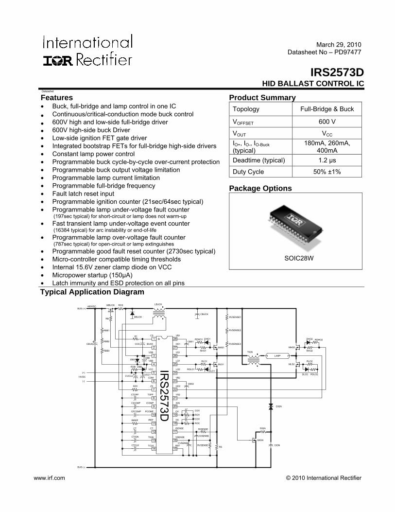
www.irf.com © 2010 International Rectifier March 29, 2010 Datasheet No – PD97477 IRS2573D HID BALLAST CONTROL IC Datasehet Features • Buck, full-bridge and lamp control in one IC • Continuous/critical-conduction mode buck control • 600V high and low-side full-bridge driver • 600V high-side buck Driver • Low-side ignition FET gate driver • Integrated bootstrap FETs for full-bridge high-side drivers • Constant lamp power control • Programmable buck cycle-by-cycle over-current protection • Programmable buck output voltage limitation • Programmable lamp current limitation • Programmable full-bridge frequency • Fault latch reset input • Programmable ignition counter (21sec/64sec typical) • Programmable lamp under-voltage fault counter (197sec typical) for short-circuit or lamp does not warm-up • Fast transient lamp under-voltage event counter (16384 typical) for arc instability or end-of-life • Programmable lamp over-voltage fault counter (787sec typical) for open-circuit or lamp extinguishes • Programmable good fault reset counter (2730sec typical) • Micro-controller compatible timing thresholds • Internal 15.6V zener clamp diode on VCC • Micropower startup (150μA) • Latch immunity and ESD protection on all pins Product Summary Topology Full-Bridge & Buck V OFFSET 600 V V OUT V CC I O+ , I O- , I O-Buck (typical) 180mA, 260mA, 400mA Deadtime (typical) 1.2 μs Duty Cycle 50% ±1% Package Options SOIC28W Typical Application Diagram RVSENSE2 RVSENSE1 CICOMP RIREF CVCC1 CBB CBS1 RHO1 RS MLS1 RISENSE RLO1 MHS1 CT CVSENSE CISENSE CBS2 RHO2 MLS2 RLO2 MHS2 CVCC2 14VDC CBUCK LBUCK DBUCK MBUCK RB CTIGN 1 2 3 5 6 7 8 9 28 27 26 25 24 23 22 21 IRS2573D VBB BUCK CS ICOMP PCOMP TOFF IREF VB2 LO2 LO1 VS1 HO1 VB1 VS2 HO2 17 18 12 CT VCC COM 11 10 19 20 OV OC VSENSE ISENSE ZX MIGN CIGN TIGN RIGN DIGN RZX VSB 4 15 16 14 TIGN TCLK 13 RST IGN CPCOMP RCS CTOFF ROC ROV CTCLK BUS (+) BUS (-) DBB RBB3 DHO2 DLO2 DHO1 DLO1 RDB COV COV (+) (-) CBUS DBS RBB1 RBB2 RVSENSE3 400VDC LAMP R1 CCS RDHO1 RDLO1 RDHO2 RDLO2 RVSENSE

Welcome message from author
This document is posted to help you gain knowledge. Please leave a comment to let me know what you think about it! Share it to your friends and learn new things together.
Transcript
www.irf.com © 2010 International Rectifier
March 29, 2010 Datasheet No – PD97477
IRS2573DHID BALLAST CONTROL IC
Datasehet
Features • Buck, full-bridge and lamp control in one IC • Continuous/critical-conduction mode buck control • 600V high and low-side full-bridge driver • 600V high-side buck Driver • Low-side ignition FET gate driver • Integrated bootstrap FETs for full-bridge high-side drivers • Constant lamp power control • Programmable buck cycle-by-cycle over-current protection • Programmable buck output voltage limitation • Programmable lamp current limitation • Programmable full-bridge frequency • Fault latch reset input • Programmable ignition counter (21sec/64sec typical) • Programmable lamp under-voltage fault counter
(197sec typical) for short-circuit or lamp does not warm-up • Fast transient lamp under-voltage event counter
(16384 typical) for arc instability or end-of-life • Programmable lamp over-voltage fault counter
(787sec typical) for open-circuit or lamp extinguishes • Programmable good fault reset counter (2730sec typical) • Micro-controller compatible timing thresholds • Internal 15.6V zener clamp diode on VCC • Micropower startup (150µA) • Latch immunity and ESD protection on all pins
Product Summary Topology Full-Bridge & Buck
VOFFSET 600 V
VOUT VCC
IO+, IO-, IO-Buck (typical)
180mA, 260mA, 400mA
Deadtime (typical) 1.2 µs
Duty Cycle 50% ±1% Package Options
SOIC28W
Typical Application Diagram
RVSENSE2
RVSENSE1
CICOMP
RIREF
CVCC1
CBB
CBS1
RHO1
RS
MLS1
RISENSE
RLO1
MHS1
CT
CVSENSE
CISENSE
CBS2
RHO2
MLS2RLO2
MHS2
CVCC214VDC
CBUCK
LBUCK
DBUCK
MBUCK
RB
CTIGN
1
2
3
5
6
7
8
9
28
27
26
25
24
23
22
21
IRS
2573D
VBB
BUCK
CS
ICOMP
PCOMP
TOFF
IREF
VB2
LO2
LO1
VS1
HO1
VB1
VS2
HO2
17
18
12CT
VCC
COM
11
10 19
20OV
OC
VSENSE
ISENSE
ZX
MIGN
CIGN
TIGN
RIGN
DIGN
RZX
VSB
4
15
16
14
TIGN
TCLK
13
RST
IGN
CPCOMP
RCS
CTOFF
ROC
ROV
CTCLK
BUS (+)
BUS (-)
DBB
RBB3
DHO2
DLO2
DHO1
DLO1
RDB
COV
COV
(+)
(-)
CBUS
DBS
RBB1
RBB2RVSENSE3
400VDC
LAMP
R1
CCS
RDHO1
RDLO1
RDHO2
RDLO2
RVSENSE
IRS2573D
www.irf.com © 2009 International Rectifier 2
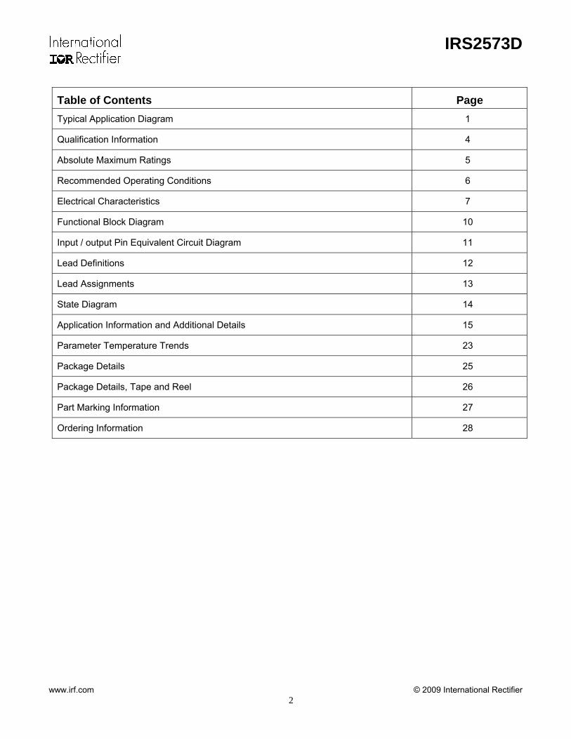
Table of Contents Page Typical Application Diagram 1
Qualification Information 4
Absolute Maximum Ratings 5
Recommended Operating Conditions 6
Electrical Characteristics 7
Functional Block Diagram 10
Input / output Pin Equivalent Circuit Diagram 11
Lead Definitions 12
Lead Assignments 13
State Diagram 14
Application Information and Additional Details 15
Parameter Temperature Trends 23
Package Details 25
Package Details, Tape and Reel 26
Part Marking Information 27
Ordering Information 28
IRS2573D
www.irf.com © 2009 International Rectifier 3
Description The IRS2573D is a fully-integrated, fully-protected 600V HID control IC designed to drive all types of HID lamps. Internal circuitry provides control for ignition, warm-up, running and fault operating modes. The IRS2573D features include ignition timing control, constant lamp power control, programmable full-bridge running frequency, programmable over and under-voltage protection and programmable over-current protection. Advanced protection features such as failure of a lamp to ignite, open load, short-circuit and a programmable fault counter have also been included in the design.
IRS2573D
www.irf.com © 2009 International Rectifier 4
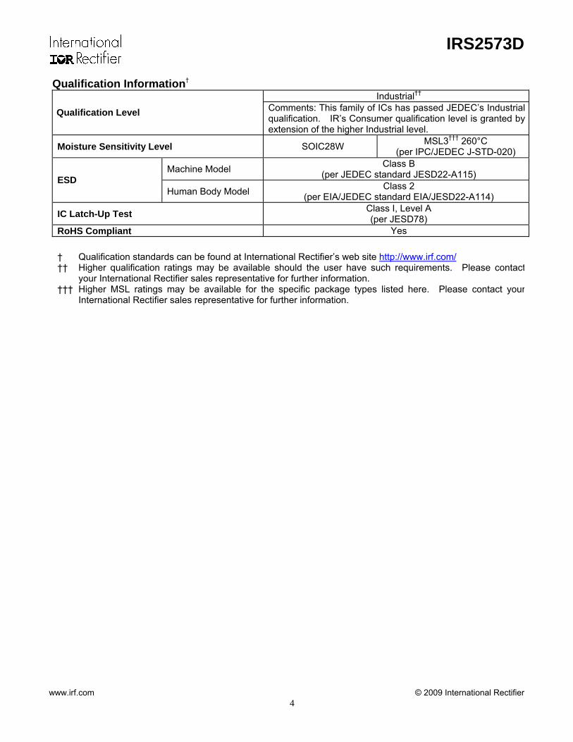
Qualification Information† Industrial††
Qualification Level Comments: This family of ICs has passed JEDEC’s Industrial qualification. IR’s Consumer qualification level is granted by extension of the higher Industrial level.
Moisture Sensitivity Level SOIC28W MSL3††† 260°C (per IPC/JEDEC J-STD-020)
Machine Model Class B (per JEDEC standard JESD22-A115) ESD
Human Body Model Class 2 (per EIA/JEDEC standard EIA/JESD22-A114)
IC Latch-Up Test Class I, Level A (per JESD78)
RoHS Compliant Yes
† Qualification standards can be found at International Rectifier’s web site http://www.irf.com/ †† Higher qualification ratings may be available should the user have such requirements. Please contact
your International Rectifier sales representative for further information. ††† Higher MSL ratings may be available for the specific package types listed here. Please contact your
International Rectifier sales representative for further information.
IRS2573D
www.irf.com © 2009 International Rectifier 5
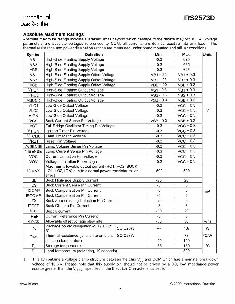
Absolute Maximum Ratings Absolute maximum ratings indicate sustained limits beyond which damage to the device may occur. All voltage parameters are absolute voltages referenced to COM, all currents are defined positive into any lead. The thermal resistance and power dissipation ratings are measured under board mounted and still air conditions.
Symbol Definition Min. Max. Units VB1 High-Side Floating Supply Voltage -0.3 625 VB2 High-Side Floating Supply Voltage -0.3 625 VBB High-Side Floating Supply Voltage -0.3 625 VS1 High-Side Floating Supply Offset Voltage VB1 – 25 VB1 + 0.3 VS2 High-Side Floating Supply Offset Voltage VB2 – 25 VB2 + 0.3 VSB High-Side Floating Supply Offset Voltage VBB – 20 VBB + 0.3
VHO1 High-Side Floating Output Voltage VS1 - 0.3 VB1 + 0.3 VHO2 High-Side Floating Output Voltage VS2 - 0.3 VB2 + 0.3
VBUCK High-Side Floating Output Voltage VSB - 0.3 VBB + 0.3 VLO1 Low-Side Output Voltage -0.3 VCC + 0.3 VLO2 Low-Side Output Voltage -0.3 VCC + 0.3 VIGN Low-Side Output Voltage -0.3 VCC + 0.3 VCS Buck Current Sense Pin Voltage VSB - 0.3 VBB + 0.3 VCT Full-Bridge Oscillator Timing Pin Voltage -0.3 VCC + 0.3
VTIGN Ignition Timer Pin Voltage -0.3 VCC + 0.3 VTCLK Fault Timer Pin Voltage -0.3 VCC + 0.3 VRST Reset Pin Voltage -0.3 VCC + 0.3
VVSENSE Lamp Voltage Sense Pin Voltage -0.3 VCC + 0.3 VISENSE Lamp Current Sense Pin Voltage -0.3 VCC + 0.3
VOC Current Limitation Pin Voltage -0.3 VCC + 0.3 VOV Voltage Limitation Pin Voltage -0.3 VCC + 0.3
V
IOMAX Maximum allowable output current (HO1, HO2, BUCK, LO1, LO2, IGN) due to external power transistor miller effect
-500 500
IBB Buck High-side Supply Current -20 20 ICS Buck Current Sense Pin Current -5 5
IICOMP Buck Compensation Pin Current -5 5 IPCOMP Buck Compensation Pin Current -5 5
IZX Buck Zero-crossing Detection Pin Current -5 5 ITOFF Buck Off-time Pin Current -5 5
ICC Supply current† -20 20
IIREF Current Reference Pin Current -5 5
mA
dVS/dt Allowable offset voltage slew rate -50 50 V/ns
PD Package power dissipation @ TA ≤ +25 ºC SOIC28W --- 1.6 W
RΘJA Thermal resistance, junction to ambient SOIC28W --- 78 ºC/W TJ Junction temperature -55 150 TS Storage temperature -55 150 TL Lead temperature (soldering, 10 seconds) --- 300
ºC
† This IC contains a voltage clamp structure between the chip VCC and COM which has a nominal breakdown
voltage of 15.6 V. Please note that this supply pin should not be driven by a DC, low impedance power source greater than the VCLAMP specified in the Electrical Characteristics section.
IRS2573D
www.irf.com © 2009 International Rectifier 6
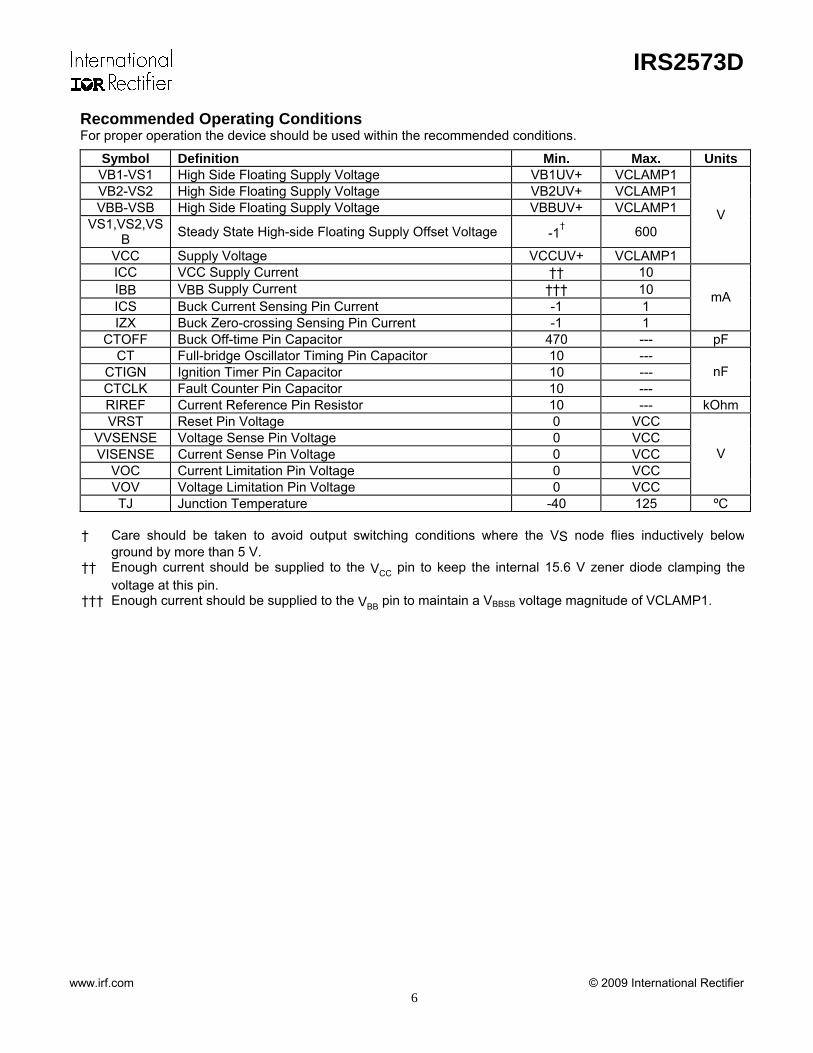
Recommended Operating Conditions For proper operation the device should be used within the recommended conditions.
Symbol Definition Min. Max. Units VB1-VS1 High Side Floating Supply Voltage VB1UV+ VCLAMP1 VB2-VS2 High Side Floating Supply Voltage VB2UV+ VCLAMP1 VBB-VSB High Side Floating Supply Voltage VBBUV+ VCLAMP1
VS1,VS2,VSB Steady State High-side Floating Supply Offset Voltage -1
† 600
VCC Supply Voltage VCCUV+ VCLAMP1
V
ICC VCC Supply Current †† 10 IBB VBB Supply Current ††† 10 ICS Buck Current Sensing Pin Current -1 1 IZX Buck Zero-crossing Sensing Pin Current -1 1
mA
CTOFF Buck Off-time Pin Capacitor 470 --- pF CT Full-bridge Oscillator Timing Pin Capacitor 10 ---
CTIGN Ignition Timer Pin Capacitor 10 --- CTCLK Fault Counter Pin Capacitor 10 ---
nF
RIREF Current Reference Pin Resistor 10 --- kOhm VRST Reset Pin Voltage 0 VCC
VVSENSE Voltage Sense Pin Voltage 0 VCC VISENSE Current Sense Pin Voltage 0 VCC
VOC Current Limitation Pin Voltage 0 VCC VOV Voltage Limitation Pin Voltage 0 VCC
V
TJ Junction Temperature -40 125 ºC
† Care should be taken to avoid output switching conditions where the VS node flies inductively belowground by more than 5 V.
†† Enough current should be supplied to the VCC pin to keep the internal 15.6 V zener diode clamping thevoltage at this pin.
††† Enough current should be supplied to the VBB pin to maintain a VBBSB voltage magnitude of VCLAMP1.

IRS2573D
www.irf.com © 2009 International Rectifier 7
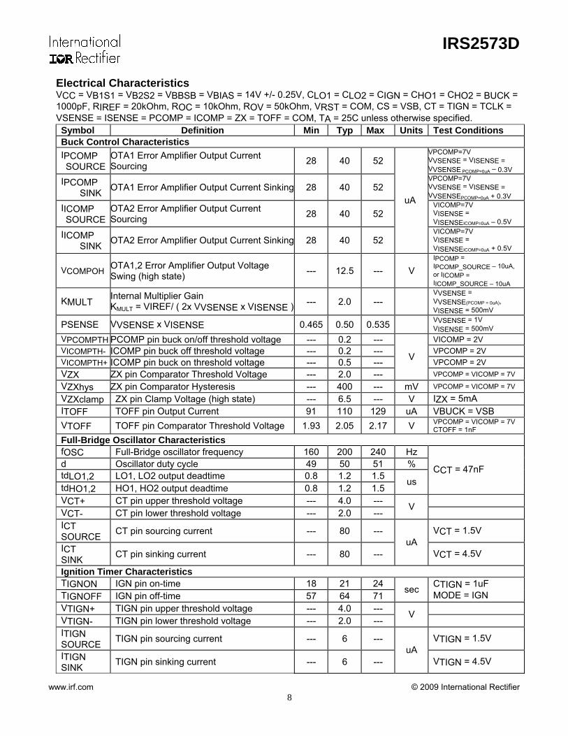
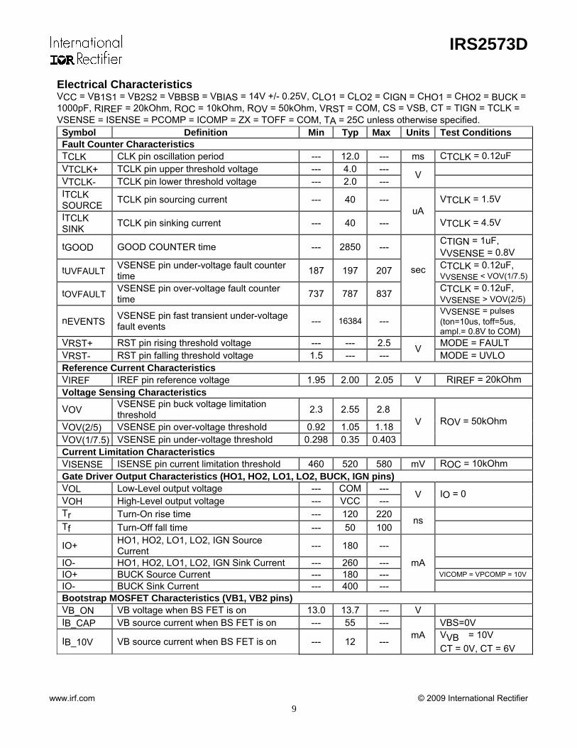
Electrical Characteristics
VCC = VB1S1 = VB2S2 = VBBSB = VBIAS = 14V +/- 0.25V, CLO1 = CLO2 = CIGN = CHO1 = CHO2 = BUCK = 1000pF, RIREF = 20kOhm, ROC = 10kOhm, ROV = 50kOhm, VRST = COM, CS = VSB, CT = TIGN = TCLK = VSENSE = ISENSE = PCOMP = ICOMP = ZX = TOFF = COM, TA = 25C unless otherwise specified. Symbol Definition Min Typ Max Units Test Conditions Supply Characteristics
VCCUV+ VCC Supply Undervoltage Positive Going Threshold 9.5 10.5 11.5 VCC rising from 0V
VCCUV- VCC Supply Undervoltage Negative Going Threshold 8.5 9.5 10.5 VCC falling from 14V
VUVHYS VCC Supply Undervoltage Lockout Hysteresis 0.5 1.0 1.5
V
IQCCUV UVLO Mode VCC Quiescent Current --- 150 VCC = 9V IQCCFLT Fault Mode VCC Quiescent Current --- 420
µA
IQCC Quiescent VCC Supply Current --- 3.5 ---
ICCGM General Mode VCC Supply Current --- 5.0 --- mA
VICOMP = VPCOMP = 4V, CTOFF=1nF, CT=47nF, CTIGN=1uF, CTCLK=0.12uF,VSENSE=0.8V
VCLAMP1 VCC Zener Clamp Voltage 14.6 15.6 16.6 V ICC = 10mA Full-Bridge Floating Supply Characteristics
IQB1S1_0 Quiescent VBS Supply Current --- 50 --- VHO1 = VS1 IQB1S1_1 Quiescent VBS Supply Current --- 80 ---
µA VHO1 = VB1
VB1S1UV+ VB1S1 Supply Undervoltage Positive Going Threshold 8.0 9.0 10.0 VB1S1 rising from 0V
VB1S1UV- VB1S1 Supply Undervoltage Negative Going Threshold 7.0 8.0 9.0
V VB1S1 falling from 14V
ILKVS1 VS1 Offset Supply Leakage Current --- --- 50 VB1 = VS1 = 600V IQB2S2_0 Quiescent VBS Supply Current --- 50 --- VHO2 = VS2 IQB2S2_1 Quiescent VBS Supply Current --- 80 ---
µA VHO2 = VB2
VB2S2UV+ VB2S2 Supply Undervoltage Positive Going Threshold 8.0 9.0 10.0 VB2S2 rising from 0V
VB2S2UV- VB2S2 Supply Undervoltage Negative Going Threshold 7.0 8.0 9.0
V VB2S2 falling from 14V
ILKVS2 VS2 Offset Supply Leakage Current --- --- 50 µA VB2 = VS2 = 600V Buck Floating Supply Characteristics VCLAMP2 VBB Zener Clamp Voltage 19.8 20.8 21.8 V IBB = 10mA IQBBSB_0 Quiescent VBBSB Supply Current --- 360 µA VBUCK = VSB IBBSB VBBSB Supply Current --- 1 --- mA VICOMP = VPCOMP = 4V,
CTOFF = 1nF
VBBSBUV+ VBBSB Supply Undervoltage Positive Going Threshold 8.0 9.0 10.0 VBBSB rising from 0V
VICOMP = VPCOMP = 0.5V
VBBSBUV- VBBSB Supply Undervoltage Negative Going Threshold 7.0 8.0 9.0
V VBBSB falling from 14V VICOMP = VPCOMP = 0.5V
ILKVSB VSB Offset Supply Leakage Current --- --- 50 µA VBB = VSB = 600V VCS CS pin over-current threshold 1.03 1.18 1.33 V tBLANK CS pin current-sensing blank time 50 120 190 ns
VICOMP = VPCOMP = 4V
IRS2573D
www.irf.com © 2009 International Rectifier 8
Electrical Characteristics
VCC = VB1S1 = VB2S2 = VBBSB = VBIAS = 14V +/- 0.25V, CLO1 = CLO2 = CIGN = CHO1 = CHO2 = BUCK = 1000pF, RIREF = 20kOhm, ROC = 10kOhm, ROV = 50kOhm, VRST = COM, CS = VSB, CT = TIGN = TCLK = VSENSE = ISENSE = PCOMP = ICOMP = ZX = TOFF = COM, TA = 25C unless otherwise specified. Symbol Definition Min Typ Max Units Test Conditions Buck Control Characteristics IPCOMP SOURCE
OTA1 Error Amplifier Output Current Sourcing 28 40 52
VPCOMP=7V VVSENSE = VISENSE = VVSENSE PCOMP=0uA – 0.3V
IPCOMP SINK OTA1 Error Amplifier Output Current Sinking 28 40 52
VPCOMP=7V VVSENSE = VISENSE = VVSENSEPCOMP=0uA + 0.3V
IICOMP SOURCE
OTA2 Error Amplifier Output Current Sourcing 28 40 52
VICOMP=7V VISENSE = VISENSEICOMP=0uA – 0.5V
IICOMP SINK OTA2 Error Amplifier Output Current Sinking 28 40 52
uA
VICOMP=7V VISENSE = VISENSEICOMP=0uA + 0.5V
VCOMPOH OTA1,2 Error Amplifier Output Voltage Swing (high state) --- 12.5 --- V
IPCOMP = IPCOMP_SOURCE – 10uA, or IICOMP = IICOMP_SOURCE – 10uA
KMULT Internal Multiplier Gain KMULT = VIREF/ ( 2x VVSENSE x VISENSE ) --- 2.0 ---
VVSENSE = VVSENSE(PCOMP = 0uA), VISENSE = 500mV
PSENSE VVSENSE x VISENSE 0.465 0.50 0.535 VVSENSE = 1V VISENSE = 500mV
VPCOMPTH PCOMP pin buck on/off threshold voltage --- 0.2 --- VICOMP = 2V VICOMPTH- ICOMP pin buck off threshold voltage --- 0.2 --- VPCOMP = 2V VICOMPTH+ ICOMP pin buck on threshold voltage --- 0.5 --- VPCOMP = 2V VZX ZX pin Comparator Threshold Voltage --- 2.0 ---
V
VPCOMP = VICOMP = 7V
VZXhys ZX pin Comparator Hysteresis --- 400 --- mV VPCOMP = VICOMP = 7V
VZXclamp ZX pin Clamp Voltage (high state) --- 6.5 --- V IZX = 5mA ITOFF TOFF pin Output Current 91 110 129 uA VBUCK = VSB VTOFF TOFF pin Comparator Threshold Voltage 1.93 2.05 2.17 V VPCOMP = VICOMP = 7V
CTOFF = 1nF Full-Bridge Oscillator Characteristics fOSC Full-Bridge oscillator frequency 160 200 240 Hz d Oscillator duty cycle 49 50 51 % tdLO1,2 LO1, LO2 output deadtime 0.8 1.2 1.5 tdHO1,2 HO1, HO2 output deadtime 0.8 1.2 1.5
us CCT = 47nF
VCT+ CT pin upper threshold voltage --- 4.0 --- VCT- CT pin lower threshold voltage --- 2.0 ---
V
ICT SOURCE CT pin sourcing current --- 80 --- VCT = 1.5V
ICT SINK CT pin sinking current --- 80 ---
uA VCT = 4.5V
Ignition Timer Characteristics TIGNON IGN pin on-time 18 21 24 TIGNOFF IGN pin off-time 57 64 71
sec CTIGN = 1uF MODE = IGN
VTIGN+ TIGN pin upper threshold voltage --- 4.0 --- VTIGN- TIGN pin lower threshold voltage --- 2.0 ---
V
ITIGN SOURCE TIGN pin sourcing current --- 6 --- VTIGN = 1.5V
ITIGN SINK TIGN pin sinking current --- 6 ---
uA VTIGN = 4.5V
IRS2573D
www.irf.com © 2009 International Rectifier 9
Electrical Characteristics
VCC = VB1S1 = VB2S2 = VBBSB = VBIAS = 14V +/- 0.25V, CLO1 = CLO2 = CIGN = CHO1 = CHO2 = BUCK = 1000pF, RIREF = 20kOhm, ROC = 10kOhm, ROV = 50kOhm, VRST = COM, CS = VSB, CT = TIGN = TCLK = VSENSE = ISENSE = PCOMP = ICOMP = ZX = TOFF = COM, TA = 25C unless otherwise specified. Symbol Definition Min Typ Max Units Test Conditions Fault Counter Characteristics TCLK CLK pin oscillation period --- 12.0 --- ms CTCLK = 0.12uF VTCLK+ TCLK pin upper threshold voltage --- 4.0 --- VTCLK- TCLK pin lower threshold voltage --- 2.0 ---
V
ITCLK SOURCE TCLK pin sourcing current --- 40 --- VTCLK = 1.5V
ITCLK SINK TCLK pin sinking current --- 40 ---
uA VTCLK = 4.5V
tGOOD GOOD COUNTER time --- 2850 --- CTIGN = 1uF, VVSENSE = 0.8V
tUVFAULT VSENSE pin under-voltage fault counter time 187 197 207 CTCLK = 0.12uF,
VVSENSE < VOV(1/7.5)
tOVFAULT VSENSE pin over-voltage fault counter time 737 787 837
sec
CTCLK = 0.12uF, VVSENSE > VOV(2/5)
nEVENTS VSENSE pin fast transient under-voltage fault events --- 16384 ---
VVSENSE = pulses (ton=10us, toff=5us, ampl.= 0.8V to COM)
VRST+ RST pin rising threshold voltage --- --- 2.5 MODE = FAULT VRST- RST pin falling threshold voltage 1.5 --- ---
V MODE = UVLO
Reference Current Characteristics VIREF IREF pin reference voltage 1.95 2.00 2.05 V RIREF = 20kOhm Voltage Sensing Characteristics
VOV VSENSE pin buck voltage limitation threshold 2.3 2.55 2.8
VOV(2/5) VSENSE pin over-voltage threshold 0.92 1.05 1.18 VOV(1/7.5) VSENSE pin under-voltage threshold 0.298 0.35 0.403
V ROV = 50kOhm
Current Limitation Characteristics VISENSE ISENSE pin current limitation threshold 460 520 580 mV ROC = 10kOhm Gate Driver Output Characteristics (HO1, HO2, LO1, LO2, BUCK, IGN pins) VOL Low-Level output voltage --- COM --- VOH High-Level output voltage --- VCC ---
V IO = 0
Tr Turn-On rise time --- 120 220 Tf Turn-Off fall time --- 50 100
ns
IO+ HO1, HO2, LO1, LO2, IGN Source Current --- 180 ---
IO- HO1, HO2, LO1, LO2, IGN Sink Current --- 260 --- IO+ BUCK Source Current --- 180 --- VICOMP = VPCOMP = 10V
IO- BUCK Sink Current --- 400 ---
mA
Bootstrap MOSFET Characteristics (VB1, VB2 pins) VB_ON VB voltage when BS FET is on 13.0 13.7 --- V IB_CAP VB source current when BS FET is on --- 55 --- VBS=0V
IB_10V VB source current when BS FET is on --- 12 --- mA VVB = 10V
CT = 0V, CT = 6V

IRS2573D
www.irf.com © 2009 International Rectifier 10
Functional Block Diagram
IRS2573D
www.irf.com © 2009 International Rectifier 11
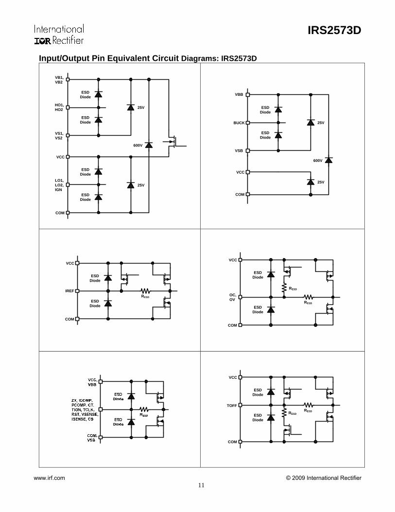
Input/Output Pin Equivalent Circuit Diagrams: IRS2573D
VCC
COM
LO1,LO2, IGN
ESD Diode
ESD Diode
VB1, VB2
VS1, VS2
HO1, HO2
ESD Diode
ESD Diode
25V
25V
600V
VCC
COM
VBB
VSB
BUCK
ESD Diode
ESD Diode
25V
25V
600V
VCC
COM
IREF
ESD Diode
ESD Diode
RESD
VCC
COM
OC, OV
ESD Diode
ESD Diode
RESD
RESD
VCC
COM
TOFF
ESD Diode
ESD Diode
RESDRESD

IRS2573D
www.irf.com © 2009 International Rectifier 12
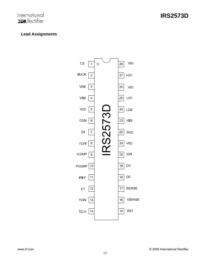
Lead Definitions
Symbol Description CS Buck Current-sensing Input
BUCK Buck High-side Floating Gate Driver Output VSB Buck High-side Floating Return VBB Buck High-side Floating Gate Driver Supply Voltage VCC IC Supply Voltage COM IC Power and Signal Ground ZX Buck Zero-Crossing Detection Input
TOFF Buck Off-time Programming Capacitor ICOMP Buck On-time Current Limit Compensation Capacitor PCOMP Buck On-time Constant Power Compensation Capacitor
IREF Current Reference Programming Resistor CT Full-Bridge Oscillator Timing Capacitor
TIGN Ignition Timer Programming Capacitor TCLK Fault Timer Programming Capacitor RST Fault Reset Input
VSENSE Lamp Voltage Sensing Input ISENSE Lamp Current Sensing Input
OV ISENSE Over-current Threshold Programming Resistor OV VSENSE Over-voltage Threshold Programming Resistor IGN Igniter Low-side Gate Driver Output VS2 Full-Bridge High-side Floating Return HO2 Full-Bridge High-side Floating Gate Driver Output VB2 Full-Bridge High-side Floating Gate Driver Supply Voltage LO2 Full-Bridge Low-side Gate Driver Output LO1 Full-Bridge Low-side Gate Driver Output VS1 Full-Bridge High-side Floating Return HO1 Full-Bridge High-side Floating Gate Driver Output VB1 Full-Bridge High-side Floating Gate Driver Supply Voltage
IRS2573D
www.irf.com © 2009 International Rectifier 13
Lead Assignments
IRS2573D
www.irf.com © 2009 International Rectifier 14
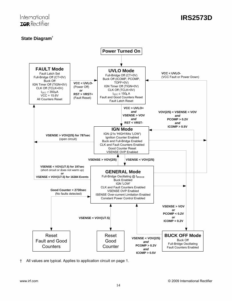
State Diagram†
VCC < UVLO-(VCC Fault or Power Down)
UVLO ModeFull-Bridge Off (CT=0V)
Buck Off (ICOMP, PCOMP, TOFF=0V)
IGN Timer Off (TIGN=0V)CLK Off (TCLK=0V)
IQCC 150 AFault and Good Counters Reset
Fault Latch Reset
GENERAL ModeFull-Bridge Oscillating @ fBRIDGE
Buck EnabledIGN 'LOW'
CLK and Fault Counters EnabledVSENSE OVP Enabled
ISENSE Over-current Limitation EnabledConstant Power Control Enabled
VCC > UVLO+and
VSENSE > VOVand
RST < VRST-
Power Turned On
FAULT ModeFault Latch Set
Full-Bridge Off (CT=0V)Buck Off
IGN Timer Off (TIGN=0V)CLK Off (TCLK=0V)
IQCC 350 AVCC = 15.6V
All Counters Reset
VCC < UVLO-(Power Off)
orRST > VRST+(Fault Reset)
VSENSE < VOV(1/7.5) for 197sec(short circuit or does not warm up)
orVSENSE < VOV(1/7.5) for 16384 Events
IGN ModeIGN (21s 'HIGH'/64s 'LOW')
Ignition Counter EnabledBuck and Full-Bridge Enabled
CLK and Fault Counters EnabledGood Counter Reset
VSENSE OVP Enabled
VSENSE < VOV(2/5)VSENSE > VOV(2/5)
VSENSE > VOV(2/5) for 787sec(open circuit)
ResetGood
Counter
Good Counter = 2730sec(No faults detected)
BUCK OFF ModeBuck Off
Full-Bridge OscillatingFault Counters Enabled
ResetFault and Good
Counters
VSENSE < VOV(1/7.5)
VOV(2/5) < VSENSE < VOVand
PCOMP > 0.2Vand
ICOMP > 0.5V
VSENSE > VOVor
PCOMP < 0.2Vor
ICOMP < 0.2V
VSENSE < VOV(2/5)and
PCOMP > 0.2Vand
ICOMP > 0.5V
† All values are typical. Applies to application circuit on page 1.
IRS2573D
www.irf.com © 2009 International Rectifier 15
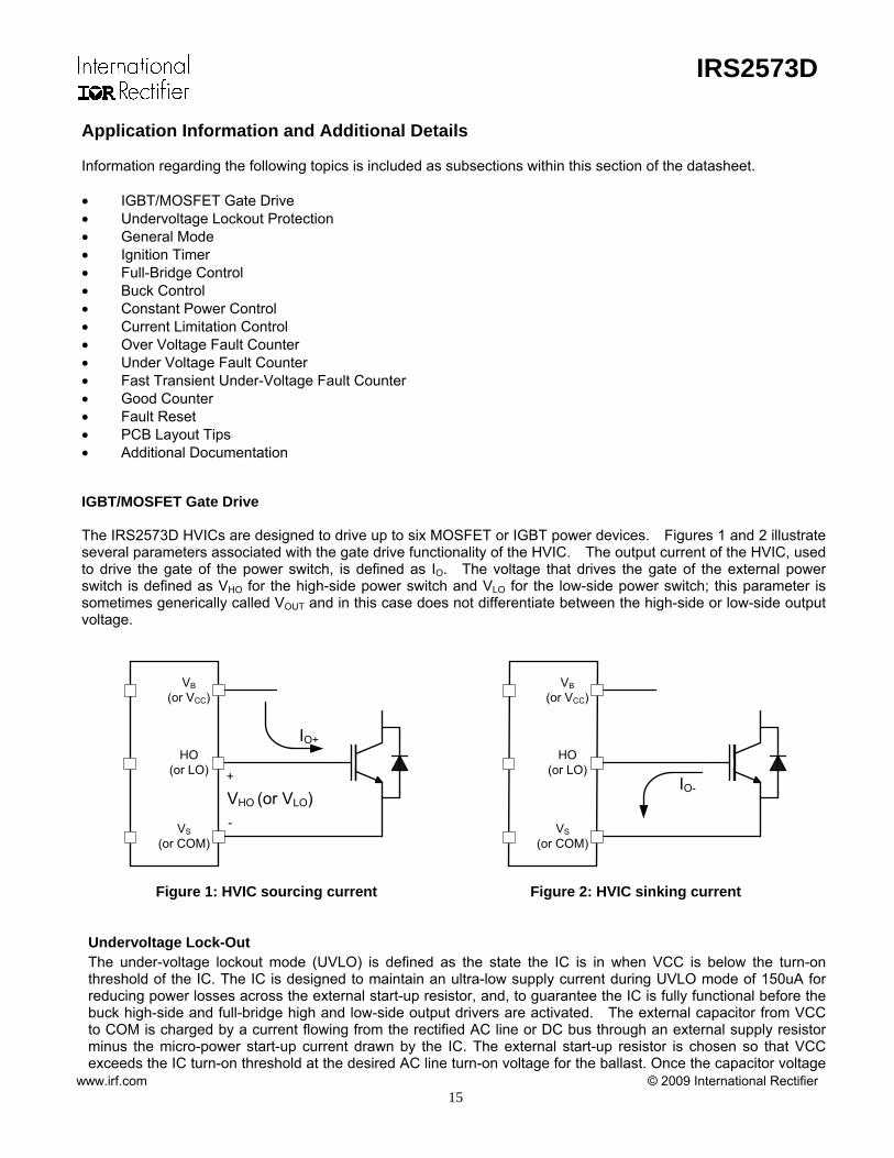
Application Information and Additional Details Information regarding the following topics is included as subsections within this section of the datasheet. • IGBT/MOSFET Gate Drive • Undervoltage Lockout Protection • General Mode • Ignition Timer • Full-Bridge Control • Buck Control • Constant Power Control • Current Limitation Control • Over Voltage Fault Counter • Under Voltage Fault Counter • Fast Transient Under-Voltage Fault Counter • Good Counter • Fault Reset • PCB Layout Tips • Additional Documentation IGBT/MOSFET Gate Drive The IRS2573D HVICs are designed to drive up to six MOSFET or IGBT power devices. Figures 1 and 2 illustrate several parameters associated with the gate drive functionality of the HVIC. The output current of the HVIC, used to drive the gate of the power switch, is defined as IO. The voltage that drives the gate of the external power switch is defined as VHO for the high-side power switch and VLO for the low-side power switch; this parameter is sometimes generically called VOUT and in this case does not differentiate between the high-side or low-side output voltage.
VS(or COM)
HO(or LO)
VB(or VCC)
IO+
VHO (or VLO)+
-
VS(or COM)
HO(or LO)
VB(or VCC)
IO-
Figure 1: HVIC sourcing current Figure 2: HVIC sinking current
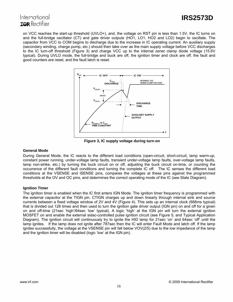
Undervoltage Lock-Out The under-voltage lockout mode (UVLO) is defined as the state the IC is in when VCC is below the turn-on threshold of the IC. The IC is designed to maintain an ultra-low supply current during UVLO mode of 150uA for reducing power losses across the external start-up resistor, and, to guarantee the IC is fully functional before the buck high-side and full-bridge high and low-side output drivers are activated. The external capacitor from VCC to COM is charged by a current flowing from the rectified AC line or DC bus through an external supply resistor minus the micro-power start-up current drawn by the IC. The external start-up resistor is chosen so that VCC exceeds the IC turn-on threshold at the desired AC line turn-on voltage for the ballast. Once the capacitor voltage
IRS2573D
www.irf.com © 2009 International Rectifier 16
on VCC reaches the start-up threshold (UVLO+), and, the voltage on RST pin is less than 1.5V, the IC turns on and the full-bridge oscillator (CT) and gate driver outputs (HO1, LO1, HO2 and LO2) begin to oscillate. The capacitor from VCC to COM begins to discharge due to the increase in IC operating current. An auxiliary supply (secondary winding, charge pump, etc.) should then take over as the main supply voltage before VCC discharges to the IC turn-off threshold (Figure 3) and charge VCC up to the internal zener clamp diode voltage (15.6V typical). During UVLO mode, the full-bridge and buck are off, the ignition timer and clock are off, the fault and good counters are reset, and the fault latch is reset.
DISCHARGETIME
INTERNAL VCCZENER CLAMP VOLTAGE
VHYST
VUVLO+
VUVLO-
AUXILIARY SUPPLYOUTPUT
t
VCC
RSUPPLY & CVCCTIME CONSTANT
CVCCDISCHARGE
IC 'OFF' IC 'ON'
Figure 3, IC supply voltage during turn-on
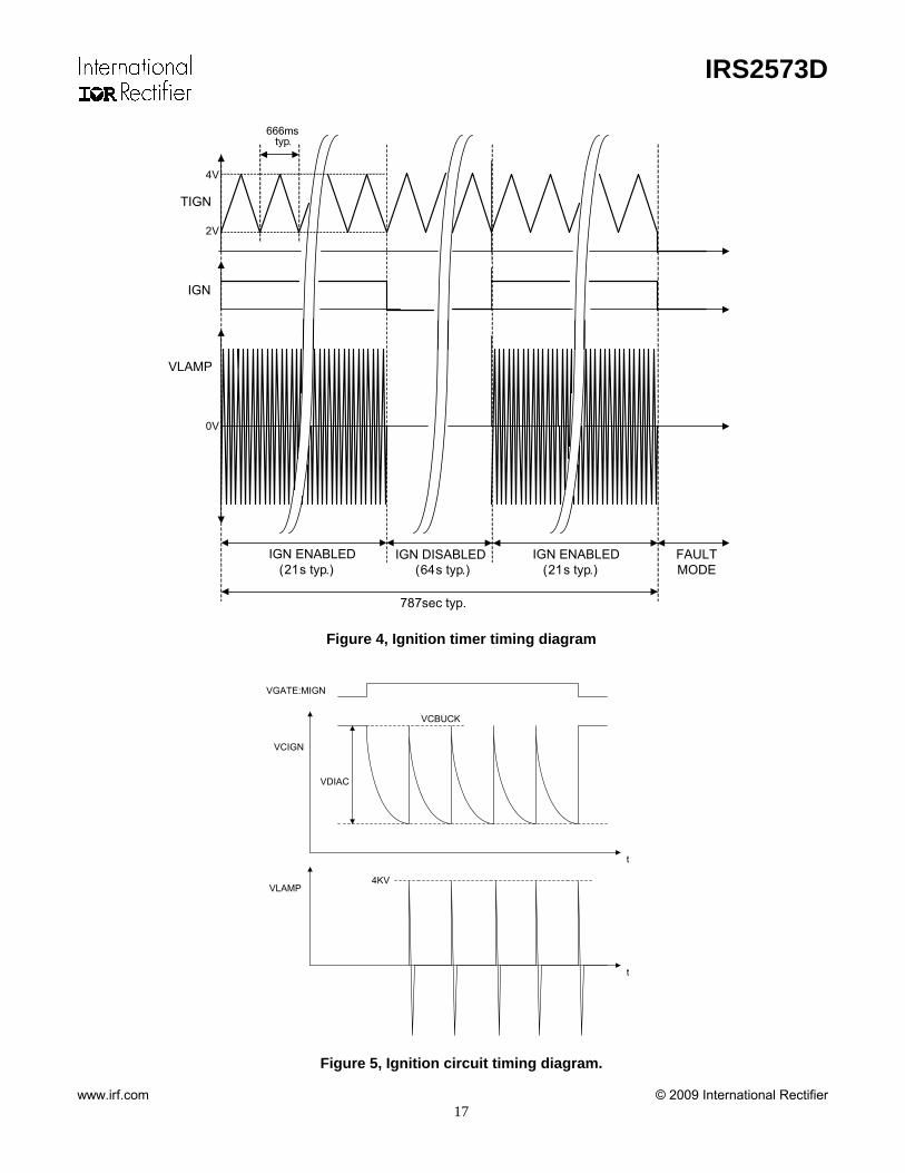
General Mode During General Mode, the IC reacts to the different load conditions (open-circuit, short-circuit, lamp warm-up, constant power running, under-voltage lamp faults, transient under-voltage lamp faults, over-voltage lamp faults, lamp non-strike, etc.) by turning the buck circuit on or off, adjusting the buck circuit on-time, or counting the occurrence of the different fault conditions and turning the complete IC off. The IC senses the different load conditions at the VSENSE and ISENSE pins, compares the voltages at these pins against the programmed thresholds at the OV and OC pins, and determines the correct operating mode of the IC (see State Diagram). Ignition Timer The ignition timer is enabled when the IC first enters IGN Mode. The ignition timer frequency is programmed with the external capacitor at the TIGN pin. CTIGN charges up and down linearly through internal sink and source currents between a fixed voltage window of 2V and 4V (Figure 4). This sets up an internal clock (666ms typical) that is divided out 128 times and then used to turn the ignition gate driver output (IGN pin) on and off for a given on and off-time (21sec ‘high’/64sec ‘low’ typical). A logic ‘high’ at the IGN pin will turn the external ignition MOSFET on and enable the external sidac-controlled pulse ignition circuit (see Figure 5, and Typical Application Diagram). The ignition circuit will continuously try to ignite the HID lamp for 21sec ‘on’ and 64sec ‘off’ until the lamp ignites. If the lamp does not ignite after 787sec then the IC will enter Fault Mode and latch off. If the lamp ignites successfully, the voltage at the VSENSE pin will fall below VOV(2/5) due to the low impedance of the lamp and the ignition timer will be disabled (logic ‘low’ at the IGN pin).
IRS2573D
www.irf.com © 2009 International Rectifier 17
TIGN
IGN
VLAMP
4V
2V
0V
IGN ENABLED(21s typ.)
IGN DISABLED
666ms typ.
(64s typ.)
IGN ENABLED(21s typ.)
FAULTMODE
787sec typ.
Figure 4, Ignition timer timing diagram
VLAMP4KV
VCIGN
VGATE:MIGN
VDIAC
t
t
VCBUCK
Figure 5, Ignition circuit timing diagram.

IRS2573D
www.irf.com © 2009 International Rectifier 18
Full-Bridge Control The IC includes a complete high and low-side full-bridge driver necessary for driving the HID lamp with an AC square-wave voltage. The full-bridge begins oscillating at the programmed frequency immediately when the IC comes out of UVLO Mode and turns on. The full-bridge is typically driven at a low frequency to prevent acoustic resonances from damaging the lamp. The full-bridge frequency is programmed with the external capacitor at the CT pin. CT charges up and down linearly through internal sink and source currents between a fixed voltage window of 2V and 4V. CT reaching 4V initiates the toggling of LO1/HO1, and LO2/HO2 respectively (see Figure 6). The dead-time is fixed internally at 1.0us typical. During the dead-time, all full-bridge MOSFETs are off and the mid-points of each half-bridge are floating or unbiased. Should an external transient occur during the dead-time due to an ignition voltage pulse, each half-bridge mid-point (VS1 and VS2 pins) can slew high or low very quickly and exceed the dv/dt rating of the IC. To prevent this, internal logic guarantees that the IGN pin is set to a logic ‘low’ during the dead-time. No ignition pulses can occur until the dead-time has ended and the appropriate full-bridge MOSFETs are turned on. This will guarantee that the mid-points are biased to the output voltage of the buck or COM before an ignition pulse occurs. The full-bridge stops oscillating only when the IC enters Fault Mode or UVLO Mode.
CT
LO1, HO2
LO2, HO1
VS1
VS2
VLAMP
4V
2V
0V
Dead-time Dead-time
Figure 6, Full-bridge Timing Diagram
Buck Control The buck control circuit operates in critical-conduction mode or continuous-conduction mode depending on the
off-time of the buck output or the peak current flowing through the buck MOSFET. During normal lamp running conditions, the voltage across the buck current sensing resistor, as measured by the CS pin, is below the internal over-current threshold (1.2V typical). The buck on-time is defined by the time it takes for the internal on-time capacitor to charge up to the voltage level on the PCOMP pin or ICOMP pin, whichever is lower. During the on-

IRS2573D
www.irf.com © 2009 International Rectifier 19
time, the current in the buck inductor charges up to a peak level, depending on the inductance value, and the secondary winding output of the buck inductor is at some negative voltage level, depending on the ratio between the primary and secondary windings. The secondary winding output is measured by the ZX pin, which clamps the negative voltage to a diode drop below COM using the internal ESD diode, and limits the resulting negative current flowing out of the pin with an external resistor, RZX. When the voltage on the internal on-time capacitor exceeds the voltage on the PCOMP pin or ICOMP pin, the on-time has ended and the buck output turns off. The secondary winding output of the buck inductor transitions to some positive voltage level, depending on the ratio between the primary and secondary windings, and causes the ZX pin to exceed the internal 2V threshold. The current in the buck inductor begins to discharge into the lamp full-bridge output stage. When the inductor current reaches zero, the ZX pin decreases back below the 2V threshold. This causes the internal logic of the buck control to start the on-time cycle again. This mode of operation is known as critical-conduction mode because the buck MOSFET is turned on each cycle when the inductor current discharges to zero. The on-time is programmed by the voltage level on the PCOMP pin, and the off-time is determined by the time it takes for the inductor current to discharge to zero, as measured by a negative-going edge on the ZX pin (Figure 7). The resulting shape of the current in the inductor is triangular with a peak value determined by the inductance value and on-time setting. During lamp warm-up or a short-circuit condition at the output, the inductor current will charge up to an excessive
level that can saturate the inductor or damage the buck MOSFET. To prevent this condition, the buck current sensing resistor is set such that the voltage at the CS pin exceeds the internal over-current threshold (1.2V typical) before the inductor saturates. Should the CS pin exceed 1.2V before the internal on-time capacitor reaches the voltage level on the PCOMP pin or ICOMP pin, the on-time will end and the buck output will turn off. The off-time is determined by a negative-going edge on the ZX pin, or, if the maximum off time is reached as programmed by the time it takes for the external capacitor on the TOFF pin to charge up to an internal threshold of 2V. If the maximum off-time is reached before the inductor current discharges to zero, then the inductor will begin charging again from some value above zero. This mode of operation is known as continuous-conduction mode and results in a continuous DC current in the inductor with a ripple bounded above by the over-current threshold and below by the maximum off time setting. Continuous-conduction mode also allows for a higher average current to flow through the buck inductor before saturation occurs than with critical-conduction mode.
VCC UVLO+
0.2V
VPCOMP
CTON
ZX
BUCK
2V
TOFF
Critical Conduction Mode Continuous Conduction Mode
1.2V
ILBUCK
Figure 7, Buck circuit timing diagram
IRS2573D
www.irf.com © 2009 International Rectifier 20
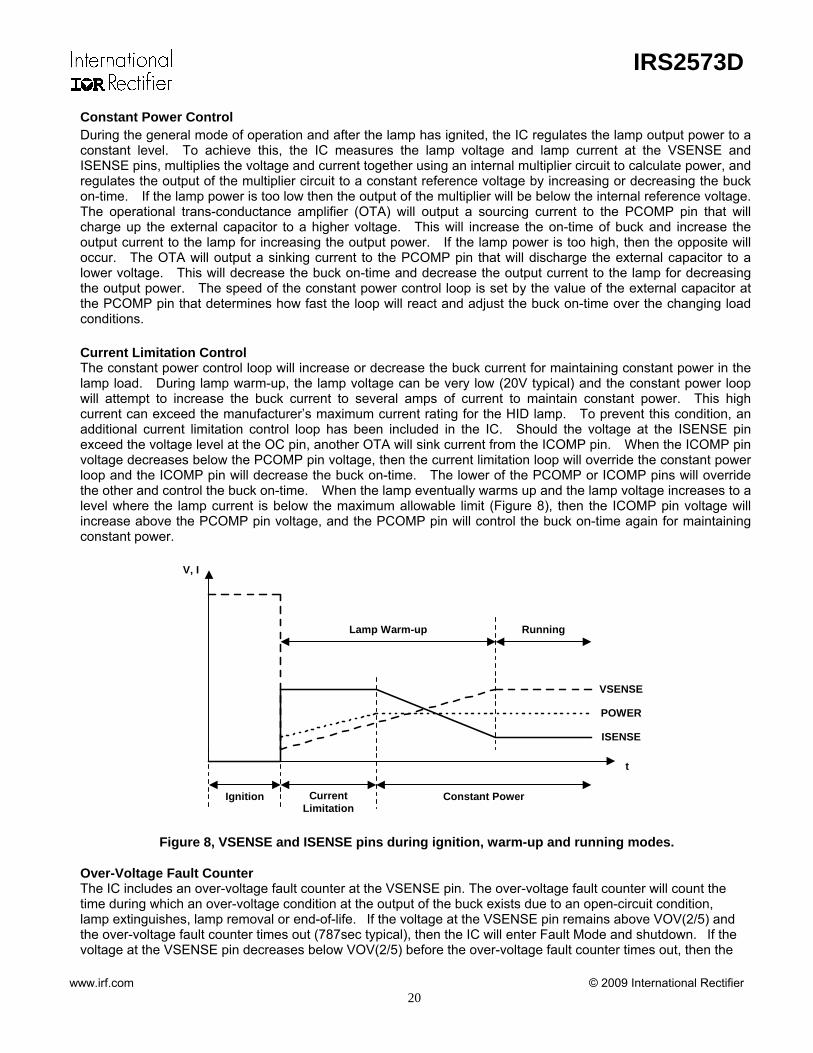
Constant Power Control During the general mode of operation and after the lamp has ignited, the IC regulates the lamp output power to a constant level. To achieve this, the IC measures the lamp voltage and lamp current at the VSENSE and ISENSE pins, multiplies the voltage and current together using an internal multiplier circuit to calculate power, and regulates the output of the multiplier circuit to a constant reference voltage by increasing or decreasing the buck on-time. If the lamp power is too low then the output of the multiplier will be below the internal reference voltage. The operational trans-conductance amplifier (OTA) will output a sourcing current to the PCOMP pin that will charge up the external capacitor to a higher voltage. This will increase the on-time of buck and increase the output current to the lamp for increasing the output power. If the lamp power is too high, then the opposite will occur. The OTA will output a sinking current to the PCOMP pin that will discharge the external capacitor to a lower voltage. This will decrease the buck on-time and decrease the output current to the lamp for decreasing the output power. The speed of the constant power control loop is set by the value of the external capacitor at the PCOMP pin that determines how fast the loop will react and adjust the buck on-time over the changing load conditions. Current Limitation Control The constant power control loop will increase or decrease the buck current for maintaining constant power in the lamp load. During lamp warm-up, the lamp voltage can be very low (20V typical) and the constant power loop will attempt to increase the buck current to several amps of current to maintain constant power. This high current can exceed the manufacturer’s maximum current rating for the HID lamp. To prevent this condition, an additional current limitation control loop has been included in the IC. Should the voltage at the ISENSE pin exceed the voltage level at the OC pin, another OTA will sink current from the ICOMP pin. When the ICOMP pin voltage decreases below the PCOMP pin voltage, then the current limitation loop will override the constant power loop and the ICOMP pin will decrease the buck on-time. The lower of the PCOMP or ICOMP pins will override the other and control the buck on-time. When the lamp eventually warms up and the lamp voltage increases to a level where the lamp current is below the maximum allowable limit (Figure 8), then the ICOMP pin voltage will increase above the PCOMP pin voltage, and the PCOMP pin will control the buck on-time again for maintaining constant power.
CurrentLimitation
Lamp Warm-up
Ignition
Running
Constant Power
V, I
t
VSENSE
ISENSE
POWER
Figure 8, VSENSE and ISENSE pins during ignition, warm-up and running modes. Over-Voltage Fault Counter The IC includes an over-voltage fault counter at the VSENSE pin. The over-voltage fault counter will count the time during which an over-voltage condition at the output of the buck exists due to an open-circuit condition, lamp extinguishes, lamp removal or end-of-life. If the voltage at the VSENSE pin remains above VOV(2/5) and the over-voltage fault counter times out (787sec typical), then the IC will enter Fault Mode and shutdown. If the voltage at the VSENSE pin decreases below VOV(2/5) before the over-voltage fault counter times out, then the
IRS2573D
www.irf.com © 2009 International Rectifier 21
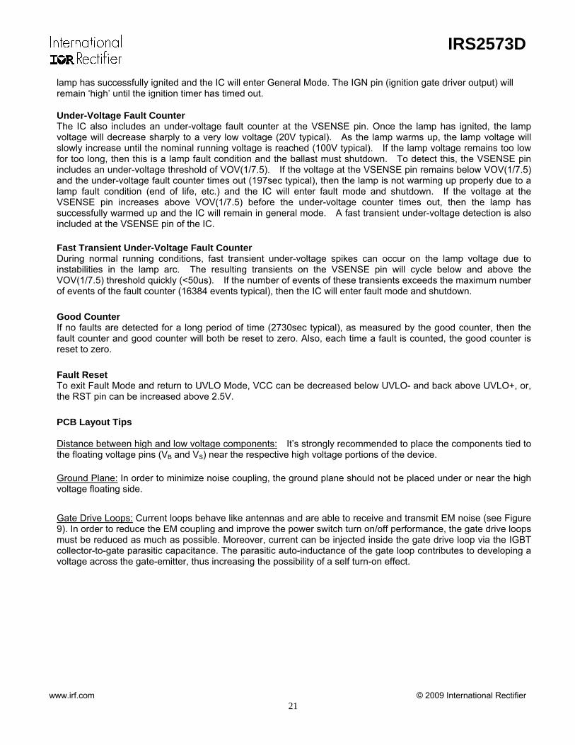
lamp has successfully ignited and the IC will enter General Mode. The IGN pin (ignition gate driver output) will remain ‘high’ until the ignition timer has timed out. Under-Voltage Fault Counter The IC also includes an under-voltage fault counter at the VSENSE pin. Once the lamp has ignited, the lamp voltage will decrease sharply to a very low voltage (20V typical). As the lamp warms up, the lamp voltage will slowly increase until the nominal running voltage is reached (100V typical). If the lamp voltage remains too low for too long, then this is a lamp fault condition and the ballast must shutdown. To detect this, the VSENSE pin includes an under-voltage threshold of VOV(1/7.5). If the voltage at the VSENSE pin remains below VOV(1/7.5) and the under-voltage fault counter times out (197sec typical), then the lamp is not warming up properly due to a lamp fault condition (end of life, etc.) and the IC will enter fault mode and shutdown. If the voltage at the VSENSE pin increases above VOV(1/7.5) before the under-voltage counter times out, then the lamp has successfully warmed up and the IC will remain in general mode. A fast transient under-voltage detection is also included at the VSENSE pin of the IC. Fast Transient Under-Voltage Fault Counter During normal running conditions, fast transient under-voltage spikes can occur on the lamp voltage due to instabilities in the lamp arc. The resulting transients on the VSENSE pin will cycle below and above the VOV(1/7.5) threshold quickly (<50us). If the number of events of these transients exceeds the maximum number of events of the fault counter (16384 events typical), then the IC will enter fault mode and shutdown. Good Counter If no faults are detected for a long period of time (2730sec typical), as measured by the good counter, then the fault counter and good counter will both be reset to zero. Also, each time a fault is counted, the good counter is reset to zero. Fault Reset To exit Fault Mode and return to UVLO Mode, VCC can be decreased below UVLO- and back above UVLO+, or, the RST pin can be increased above 2.5V. PCB Layout Tips Distance between high and low voltage components: It’s strongly recommended to place the components tied to the floating voltage pins (VB and VS) near the respective high voltage portions of the device. Ground Plane: In order to minimize noise coupling, the ground plane should not be placed under or near the high voltage floating side. Gate Drive Loops: Current loops behave like antennas and are able to receive and transmit EM noise (see Figure 9). In order to reduce the EM coupling and improve the power switch turn on/off performance, the gate drive loops must be reduced as much as possible. Moreover, current can be injected inside the gate drive loop via the IGBT collector-to-gate parasitic capacitance. The parasitic auto-inductance of the gate loop contributes to developing a voltage across the gate-emitter, thus increasing the possibility of a self turn-on effect.
IRS2573D
www.irf.com © 2009 International Rectifier 22
Figure 9: Antenna Loops Supply Capacitor: It is recommended to place a bypass capacitor (CIN) between the VCC and VSS pins. A ceramic 1 μF ceramic capacitor is suitable for most applications. This component should be placed as close as possible to the pins in order to reduce parasitic elements. Routing and Placement: Power stage PCB parasitic elements can contribute to large negative voltage transients as the switch node; it is recommended to limit the phase voltage negative transients. In order to avoid such conditions, it is recommended to 1) minimize the high-side emitter to low-side collector distance, and 2) minimize the low-side emitter to negative bus rail stray inductance. However, where negative VS spikes remain excessive, further steps may be taken to reduce the spike. This includes placing a resistor (5 Ω or less) between the VS pin and the switch node (see Figure 10), and in some cases using a clamping diode between VSS and VS (see Figure 11). See DT04-4 at www.irf.com for more detailed information.
Figure 10: VS resistor Figure 11: VS clamping diode
Additional Documentation Several technical documents related to the use of HVICs are available at www.irf.com; use the Site Search function and the document number to quickly locate them. Below is a short list of some of these documents. DT97-3: Managing Transients in Control IC Driven Power Stages AN-1123: Bootstrap Network Analysis: Focusing on the Integrated Bootstrap Functionality DT04-4: Using Monolithic High Voltage Gate Drivers AN-978: HV Floating MOS-Gate Driver ICs
IRS2573D
www.irf.com © 2009 International Rectifier 23
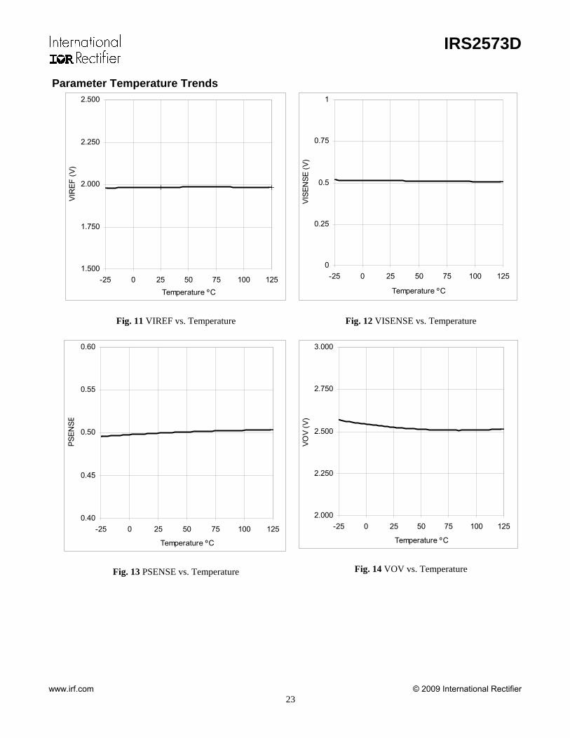
Parameter Temperature Trends
1.500
1.750
2.000
2.250
2.500
-25 0 25 50 75 100 125Temperature ºC
VIR
EF (V
)
Fig. 11 VIREF vs. Temperature
0
0.25
0.5
0.75
1
-25 0 25 50 75 100 125
Temperature ºC
VISE
NSE
(V)
Fig. 12 VISENSE vs. Temperature
0.40
0.45
0.50
0.55
0.60
-25 0 25 50 75 100 125
Temperature ºC
PSEN
SE
Fig. 13 PSENSE vs. Temperature
2.000
2.250
2.500
2.750
3.000
-25 0 25 50 75 100 125
Temperature ºC
VOV
(V)
Fig. 14 VOV vs. Temperature

IRS2573D
www.irf.com © 2009 International Rectifier 24
0.500
0.750
1.000
1.250
1.500
-25 0 25 50 75 100 125
Temperature ºC
0V(2
/5) (
V)
Fig. 15 OV(2/5) vs. Temperature
0.000
0.250
0.500
0.750
1.000
-25 0 25 50 75 100 125
Temperature ºC
0V(1
/7.5
) (V)
Fig. 16 OV(1/7.5) vs. Temperature
0
50
100
150
200
-25 0 25 50 75 100 125
Temperature ºC
ITO
FF (u
A)
Fig. 17 ITOFF vs. Temperature
1.500
1.750
2.000
2.250
2.500
-25 0 25 50 75 100 125Temperature ºC
VTO
FF (V
)
Fig. 18 VTOFF vs. Temperature
IRS2573D
www.irf.com © 2009 International Rectifier 25
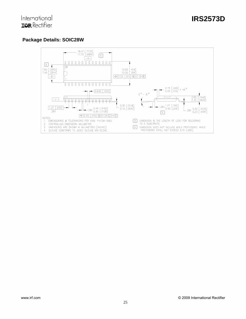
Package Details: SOIC28W
IRS2573D
www.irf.com © 2009 International Rectifier 26
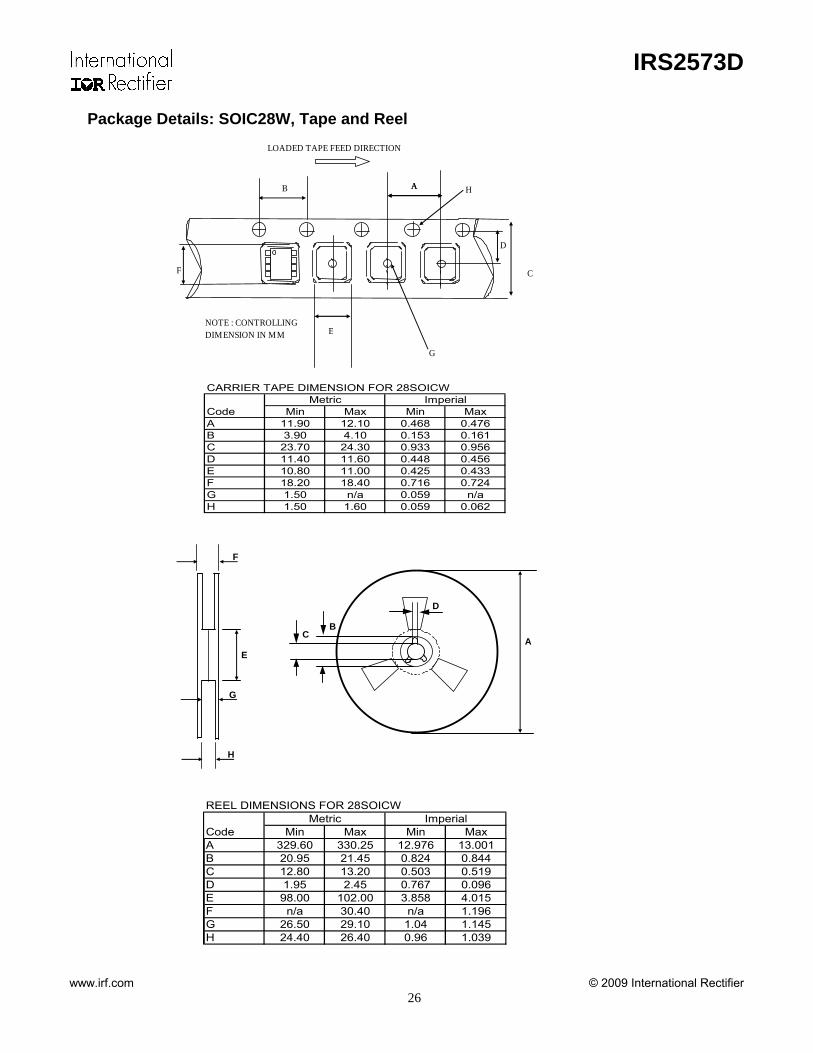
Package Details: SOIC28W, Tape and Reel
CARRIER TAPE DIMENSION FOR 28SOICW
Code Min Max Min MaxA 11.90 12.10 0.468 0.476B 3.90 4.10 0.153 0.161C 23.70 24.30 0.933 0.956D 11.40 11.60 0.448 0.456E 10.80 11.00 0.425 0.433F 18.20 18.40 0.716 0.724G 1.50 n/a 0.059 n/aH 1.50 1.60 0.059 0.062
Metric Imperial
REEL DIMENSIONS FOR 28SOICW
Code Min Max Min MaxA 329.60 330.25 12.976 13.001B 20.95 21.45 0.824 0.844C 12.80 13.20 0.503 0.519D 1.95 2.45 0.767 0.096E 98.00 102.00 3.858 4.015F n/a 30.40 n/a 1.196G 26.50 29.10 1.04 1.145H 24.40 26.40 0.96 1.039
Metric Imperial
E
F
A
C
D
G
AB H
NOTE : CONTROLLING DIMENSION IN MM
LOADED TAPE FEED DIRECTION
A
H
F
E
G
D
BC
IRS2573D
www.irf.com © 2009 International Rectifier 27
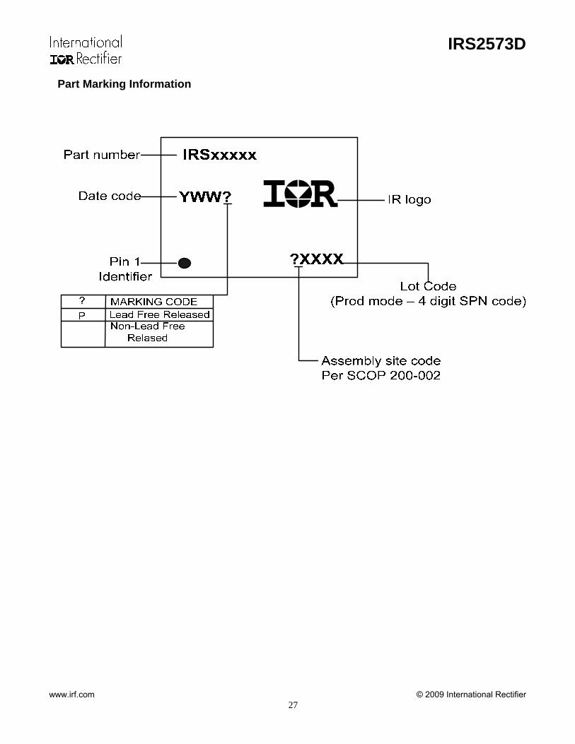
Part Marking Information
IRS2573D
www.irf.com © 2009 International Rectifier 28
Ordering Information Standard Pack
Base Part Number Package Type Form Quantity
Complete Part Number
Tube/Bulk 25 IRS2573DSPBF IRS2573D SOIC28W
Tape and Reel 1000 IRS2573DSTRPBF
The information provided in this document is believed to be accurate and reliable. However, International Rectifier assumes no responsibility for the consequences of the use of this information. International Rectifier assumes no responsibility for any infringement of patents or of other rights of third parties which may result from the use of this information. No license is granted by implication or otherwise under any
patent or patent rights of International Rectifier. The specifications mentioned in this document are subject to change without notice. This document supersedes and replaces all information previously supplied.
For technical support, please contact IR’s Technical Assistance Center http://www.irf.com/technical-info/
WORLD HEADQUARTERS:
233 Kansas St., El Segundo, California 90245 Tel: (310) 252-7105
Related Documents

![Datasheet - edison-opto.com.t Opto datasheet-HeadLamp... · 05 2016. 08. 29 Version 0.2 HeadLamp Series Brightness Groups (TS = 25 °C) Group (min.) Luminous Intensity Iv [lm] @1000mA](https://static.cupdf.com/doc/110x72/5c8fce9209d3f282338b4d43/datasheet-edison-optocomt-opto-datasheet-headlamp-05-2016-08-29-version.jpg)