INTRODUCTION TO ELECTRONIC MAINTENANCE AND REPAIRS

Welcome message from author
This document is posted to help you gain knowledge. Please leave a comment to let me know what you think about it! Share it to your friends and learn new things together.
Transcript
INTRODUCTION TO ELECTRONIC
MAINTENANCE AND REPAIRS
DR. EMMANUEL RAYMOND
DR. BASHIR BUKAR
DR. YUNUSA JAMILU HASSAN
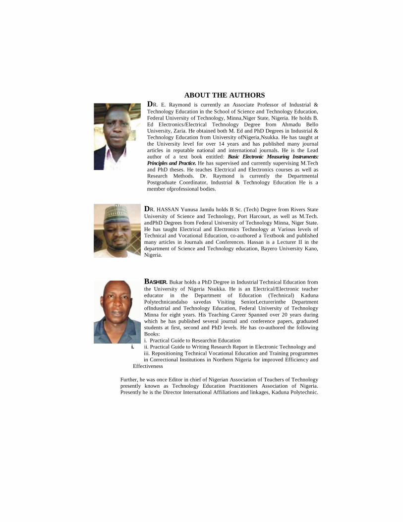
ABOUT THE AUTHORS DR. E. Raymond is currently an Associate Professor of Industrial & Technology Education in the School of Science and Technology Education, Federal University of Technology, Minna,Niger State, Nigeria. He holds B. Ed Electronics/Electrical Technology Degree from Ahmadu Bello University, Zaria. He obtained both M. Ed and PhD Degrees in Industrial & Technology Education from University ofNigeria,Nsukka. He has taught at the University level for over 14 years and has published many journal articles in reputable national and international journals. He is the Lead author of a text book entitled: Basic Electronic Measuring Instruments: Principles and Practice. He has supervised and currently supervising M.Tech and PhD theses. He teaches Electrical and Electronics courses as well as Research Methods. Dr. Raymond is currently the Departmental Postgraduate Coordinator, Industrial & Technology Education He is a member ofprofessional bodies.
DR. HASSAN Yunusa Jamilu holds B Sc. (Tech) Degree from Rivers State University of Science and Technology, Port Harcourt, as well as M.Tech. andPhD Degrees from Federal University of Technology Minna, Niger State. He has taught Electrical and Electronics Technology at Various levels of Technical and Vocational Education, co-authored a Textbook and published many articles in Journals and Conferences. Hassan is a Lecturer II in the department of Science and Technology education, Bayero University Kano, Nigeria.
BASHER. Bukar holds a PhD Degree in Industrial Technical Education from the University of Nigeria Nsukka. He is an Electrical/Electronic teacher educator in the Department of Education (Technical) Kaduna Polytechnicandalso savedas Visiting SeniorLecturerinthe Department ofIndustrial and Technology Education, Federal University of Technology Minna for eight years. His Teaching Career Spanned over 20 years during which he has published several journal and conference papers, graduated students at first, second and PhD levels. He has co-authored the following Books: i. Practical Guide to Researchin Education
i. ii. Practical Guide to Writing Research Report in Electronic Technology and iii. Repositioning Technical Vocational Education and Training programmes in Correctional Institutions in Northern Nigeria for improved Efficiency and
Effectiveness
Further, he was once Editor in chief of Nigerian Association of Teachers of Technology presently known as Technology Education Practitioners Association of Nigeria. Presently he is the Director International Affiliations and linkages, Kaduna Polytechnic.
i
Copyright ©B. Bukar,E, Raymond & Y.J.Hassan, 2020
ISBN: 978-978-980-495-5 Authors Address
Dr. Bashir Bukar Chief Lecturer School of Education Technical Kaduna Polytechnic, Kaduna, Nigeria [email protected] Dr. Emmanuel Raymond Associate Professor of Industrial & Technology Education Federal University of Technology, Minna, Niger State, Nigeria [email protected] Dr. Yunusa Jamilu Hassan Lecturer II Department of Science and Technology Education Bayero University, Kano, Nigeria [email protected]
All rights reserved. No part of this publication may be reproduced or transmitted in any form by any means, electronic, mechanical, photocopying, recording or otherwise without the prior written permission of the author.
Printed by
UNIVERSITY PRESS LTD UsmanuDanfodiyo University, Sokoto, Nigeria

ii
Dedication
This book is dedicated to the families of the authors
iii
FOREWORD
Technology has propelled modern world into an outstanding status not just in product development but also in automation. The extent to which the world has automated her systems is dazzling and it does not seem to have gotten to her wit’s end in this development. Technology which is the driving force behind the world’s outstanding developments draws heavily from electronic principles and applications. Practical application of principles in many engagements places a demand for cognitive and psychomotor skills of manpower in the blue collar job sector which is so critical for development and self-reliance of individuals and nations.
Blue collar jobs are major essentials for industrial development and sustainable healthy economic growth of any nation or society. Blue collar jobs are essentially skilled jobs, and equipping for such jobs in a structured educational system calls for ‘mind-on hands-on’ experiences. This, the authors have taken into consideration in authoring the Book, Introduction to Electronic Maintenance and Repairs. The Book is carefully authored to provide the cognitive and psychomotor knowledge and skills that can easily engross learners into sustained study of the subject matter of electronic maintenance and repairs. The authors have included electronic principles and applications to contemporary devices, such as were not captured in older Textbooks in the subject area.
The authors, in this five-chapter Book, judiciously delivered concepts and detailed practical steps and approaches that should lead to acquisition of appropriate knowledge and functional skills in principles, tools, equipment, materials, troubleshooting, operation and practices in electronic maintenance and repairs. The blend of rich practical experiences and high academic backgrounds of the three authors coupled with broad content areas that are relevant across the three tiers of Nigerian education make the Book of high and relevant quality. The Book contains enough to empower one to be self-reliant. It is therefore an unemployment tackling textbook for anyone who will want to build skill in electronic maintenance and repairs for either self-employment or paid employment.
The hue and cry about non employability of programme graduates from educational and training institutions should be a non-issue in electronic maintenance and repairs for those who will use this Textbook in their training. The exercises at the end of each chapter of the Book provide immediate check of materials learnt at each stage. The Book, Introduction to Electronic Maintenance and Repairs portrays an intensive and comprehensive research into the subject matter lazed with great wealth of experiences. I therefore, strongly recommended it as a good resource text for all that are or will be engaged in maintenance and repairs of electronic devices.
Emmanuel J. OhizePh.D, MNAE, MTRCN, MNATT Professor of Industrial & Technology Education.
iv
TABLE OF CONTENTS
Dedication iv Foreword v Preface ix Acknowledgements
x
CHAPTER ONE 1.0 OVERVIEW OF ELECTRONIC MAINTENANCE AND REPAIRS 1 1.1 Electronic Maintenance 1 1.2 Types of Electronic Maintenance 2 1.3 Electronic Troubleshooting and Repairs 4 1.4 Components of Electronic Circuit 5 1.5 Electronic Circuit Diagrams 30 1.6 Exercises 34
CHAPTER TWO
2.0 TEST EQUIPMENT, TOOLS AND MATERIALS IN ELECTRONIC MAINTENANCE AND REPAIRS
37
2.1 Test Equipment in Electronic Maintenance and Repairs 37 2.2 Tools in Electronic Maintenance and Repairs 60 2.3 Materials Used in Electronic Maintenance and Repairs 71 2.4 Exercises 75
CHAPTER THREE
3.0 PRACTICAL TROUBLESHOOTING TECHNIQUES 78 3.1 Common Symptoms and Failures in Electronic Equipment 78 3.2 Practical Troubleshooting Techniques 82 3.3 Safety Precautions in Electronic Maintenance and Repairs 106 3.4 Exercises 110
CHAPTER FOUR
4.0 PRINCIPLES OF OPERATION OF SOME ELECTRONIC SYSTEMS
113
4.1 Principles of Operation of Digital Video Decoder 113 4.2 Principles of Operation of Car Stereo System 114
v
4.3 Principles of Operation of Radio Receiver 117 4.4 Principles of Operation of Computer System 120 4.5 Principles of Operation of Mobile Handset 123 4.6 Principles of Operation of Cathode Ray Tube (CRT) Television Receiver 130 4.7 Principles of Operation of Liquid Crystal Display (LCD) Television
Receiver 137
4.8 Principles of Operation of Light Emitting Diode (LED) Television Receiver
144
4.9 Principles of Operation of Plasma Television Receiver 148 4.10 Principles of Operation of Switch Mode Power Supply 152 4.11 Exercises 153
CHAPTER FIVE
5.0 PRACTICAL MAINTENANCE AND REPAIRS EXPERIENCES 156 5.1 Maintenance and Repairs of Digital Video Decoder 156 5.2 Maintenance and Repairs of Car Stereo System 157 5.3 Maintenance and Repairs of Radio Receiver 160 5.4 Maintenance and Repairs of Mobile Handset 161 5.5 Maintenance and Repairs of Cathode Ray Tube (CRT) Television 167 5.6 Maintenance and Repairs of Plasma Television 178 5.7 Maintenance and Repairs of Liquid Crystal Display (LCD) Television 180 5.8 Maintenance and Repairs of Light Emitting Diode (LED) Television 182 5.9 Maintenance and Repairs of Computer System 189 5.10 Maintenance and Repairs of Switch Mode Power Supply 193 5.11 Exercises 196 ANSWER TO EXERCISES 199
BIBLIOGRAPHY 200
INDEX 202
vi
Preface The high incidence of unemployment and under employment among graduates of Electronic Technology is a source of worry among stakeholders. This has given rise to the need of training materials that will provide knowledge and skills necessary for enhancing the employability of graduates such as this text book entitled: Introduction to Electronic Maintenance and Repairs.
This text book gives a clear explanation on how to maintain and repair selected electronic systems such as digital video decoder, car stereo, radio receiver, computer, mobile handset, cathode ray tube, liquid crystal display, light emitting diode and plasma television receivers as well as switch mode power supply systems. Electronic Technology Education teachers and students in secondary level and tertiary institutions as well as other readers will find this book useful in training for skills acquisition.
It is our pleasure to present this textbook to all our esteemed readers. It is sincerely hoped that the text will be useful to all.
vii
Acknowledgements
The authors wish to express their appreciation to God the provider of knowledge, wisdom, health, strength, protection and funds during the cause of writing this text book. May he be praised forever.
Further, the authors wish to place on record their gratitude to senior colleagues especially Professors B.N Atsumbe, E. J. Ohize, S. A. Ma’aji and R.O. Okwori for their unalloyed encouragement. All other colleagues are also appreciated for their friendliness.
Special thanks go to the families of the authors for the unquantifiable support and prayers they gave while writing this book.
1
CHAPTER ONE
1.0 OVERVIEW OF ELECTRONIC MAINTENANCE AND REPAIRS This chapter provides an overview of electronic maintenance and repairs. It focuses on the definition of electronic maintenance, repairs and troubleshooting, types of maintenance as well as identification of various electronic circuit components such as resistors, capacitors, transistors and Integrated Circuit (IC) with their values. At the end of this chapter therefore,the readers should be able to: Define Electronic Maintenance; DescribeDifferent Types of Electronic Maintenance; Define Electronic Troubleshooting and Repairs; IdentifyElectronic Components in a Circuit; DescribeElectronicCircuit Diagrams.
1.1 Electronic Maintenance Electronic maintenance is necessary so as to keep electronic appliances under good working condition to avoid operational downtime. Unlike mechanical parts, electronic components usually do not wear. In most cases, discrete analogue component parameters tend to change over time which can cause problems in electronicequipment that incorporate such sensitive components or designs. For instance, Integrated Circuits (ICs) can undergo electro-migration that cancause high current densities in thin-film conductors which can result to failure. Similarly,problems can occur when resistors and capacitors suddenly fail to operate as expected due to external factors such as temperature, pressure and other environmental effects in form of corrosion and vibration. Electrostatic discharge (ESD), lightning and excessive heat can also cause failure that may require immediate attention or effective maintenance of the electronic circuit.
Components’ parameters usually vary with temperature and it is important not to exceed the manufacture’s temperature range. Above such temperatures, parts are no longer guaranteed to be within specification. More so, electronic components such as ICs can generate heat in operation and when combined with ambient temperature and solar radiation, excessive heat can be built up which can result to component level, subsystem or total equipment failure.Electronic systems can emit electromagnetic radiation that can cause interference to itself or other systems. Particularly in digital systems, a conductor acting as an antenna can pick up electromagnetic signals and corrupt digital data. Thus, to keep electronic systems safe, emission of Electromagnetic Interference (EMI) must be limited as well as the system’s susceptibility to it.
Another source of electronic equipment failure may be mechanical stress which is quite common in electro-mechanical systems such as Digital Video Disc
2
(DVD)player. Furthermore, since solder has rather poor fatigue properties, heavy components should be given extra support rather than simply relying on solder connections. Cables need to be carefully supported and strapped down to avoid wear due to moving parts. Connector failure is often a common cause for electrical system failure and attention should be paid to their placement and mounting. Therefore, Electronic systems are expected to be designed to withstand mechanical shock, vibration, humidity, environmental stresses and other causes of failure.Although precautionary measures are taken to ensure reliability of electronic systemright from the manufacturing process, it is a well-known fact that failure is often inevitable. Hence, electronic maintenance is necessary since the electronic appliances we use are bound to fail or break down.
Generally, maintenance of any electronic system consists of performing some or all of the following functions: Detection, location or diagnosis, correction and verification or checking of the cause of failure inelectronic components or equipment; setting up and performing scheduled periodicor preventive inspections and replacements; troubleshootingand repairs activities on failed electronic systems or subsystems and replacement of faulty electronic components or items. Electronic maintenance involves regular and systemic application of knowledge and skill to electronic equipment and facilities to ensure their proper functionality and reduce their rate of deterioration. In addition, it includes regular examination, inspection, lubrication, testing and adjustments without prior knowledge of equipment failure.
Maintenance provides the framework for all planned maintenance activity, including the generation of work orders to correct potential problems identified through inspection. The result is a proactive (rather than reactive) maintenance, optimising equipment performance and lifespan.Therefore, electronic maintenance is of different types according to different situations. 1.2 Types of Electronic Maintenance Based on operational downtime, maintenance of any electronicsystem or equipment can be divided mainly into two types. These are preventive and corrective maintenances. Preventive maintenance is carried out to preclude inadvertent failure of the electronic system. It involves those actions performed on the electronic system or equipment to maintain uninterrupted operation within the design specifications or characteristics of the system. However, ideally as stated earlier, preventive maintenance can only keep electronic system failure to a minimum as failures must still occur. Corrective maintenance therefore is the rectification of electronic equipment or system that has failed so as to ensure restoration of proper operational condition. In the same way, electronic maintenance can be categorised into scheduled and unscheduled maintenance.
Scheduled maintenance is synonymous to preventive maintenance. It is a timely maintenance practice that is prescribed usually by professionals or the manufacturers of such electronic system so as to forestall failure or elongate equipment’s lifespan. It
3
may involve simple tasks such as cleaning of surfaces as well as more difficult tasks such as overhauling the entire system. But the most important or distinctive features of this type of maintenance is that it is scheduled, planned or periodic. It is done weekly, monthly, or after every specified number of hours within which the electronic system was operated or ran. Unscheduled maintenance on the contrary, is just like the aforementioned corrective maintenance. It is done to correct failures or short comings when the inevitable has occurred. Unscheduled maintenance may be called reactive maintenance based on the understanding of the fact that it is not planned, it just needs to be carried out to restore the serviceability status of the system.
Furthermore, electronic maintenance can be seen as being either condition-based or reliability-based. This is a broader classification as condition-based maintenance includes preventive, corrective, reactive, planned or scheduled and unscheduled maintenances. Condition-based maintenance involves all the maintenance practices that are done based on the operational condition of the electronic systems and is different from reliability-based maintenance.
Reliability–based maintenance is expensive andoriginated from the word reliability. It is the process of developing preventative maintenance programs for electronic systems used in facilities based on the reliability characteristics of those systems and economic considerations, while ensuring that safety is not compromised.Reliability-based maintenance is the type of maintenance that is usually carried out to provide and sustain all the necessary operational conditions that will prevent any accidental failure of an important and in most cases, expensive electronic system. For instance, most of the critical electronic devices in our International and Local Airports today are placed on this type of maintenance because those systems cannot afford to fail. If they do, many lives and properties will be lost. Also, critical components of spacecraft do undergo this type of maintenance. It is worthy of notice that right at the manufacturing stage, some of these critical electronic components were already studied, tested and analysedto operate under certain conditions.Some of these analyses, carried out at production plants may include: Stress De-rating and Thermal Analysis (SDTA); Failure Modes Effects and Criticality Analysis (FMECA); Fault Tree Analysis; Mean Time to Repair Analysis; Electrical and Mechanical Reliability Simulations (ERS) to ascertain the product reliability.
Product reliability performance is a major consideration for electronic technology firms. It may affect the entire company's production bottom line. Poor product reliability may raise the following questions: Will your warranty costs exceed the total predicted costs? Will the firm lose valuable reputation? To this end, reliability is defined as the probability that an electronic item, product or system will perform a required function under stated conditions for a stated period of time. A reliability prediction can be stated as the average time (usually expressed in hours) that the electronic component or system works without failure. A reliability prediction is usually established using a model before the product is manufactured or marketed. The model can predict Mean Time Between Failure (MTBF) using as little data as the
4
part type and count information. As the design progresses, the MTBF model can be updated to include analysis of thermal, electrical and other aforementioned environmental causes of failure. That notwithstanding, in some occasions as mentioned earlier, critical components may require additional reliability at user station. In essence, reliability-based maintenance is done by experts either from the manufacturing or user station to keep the electronic system serviceable and reliable for as long as practically possible. 1.3 ElectronicTroubleshooting and Repairs As stated in the foregoing section of this book, electronic troubleshooting and repair are other aspects of electronic maintenance.Electronic troubleshootingis a problem solving process in which attempts are made to identify faults in dysfunctional systems, sub-systems or components while electronic repairs can be defined as the process of fixing by replacing a dysfunctional component or parts of an electronic system.
Electronic troubleshooting is a special category of problem solving process since in addition to fixing a problem; it involves diagnosis of the cause of failure or problem. A problem arises when a goal state exists and how to achieve that goal is not immediately apparent. Problem solving therefore is the process of finding the best solution that allows movement from the present state to the goal state. Troubleshooting in electronicterms is the act of detecting, locating and rectifying faults in electronic system. Troubleshooting is a matter of: (a) fault detection, (b) fault isolation through testing, and (c) fault correction. A fault occurs in a system when there is a change in the operating characteristics of one or more components which culminate into system failure which creates a problem situation. There are all sorts of things that can go wrong with an electronic system which may result into a fault such as:Faulty power sources including dead batteries; bad connectors and loose connectors; open cables and cables connected incorrectly; input signals missing; incorrectly set controls; component failures; network problems; as well as software problems.
Therefore, effective troubleshooting of a system requires system knowledge (conceptual knowledge of how the system works), procedural knowledge (how to perform problem-solving procedures and test activities), and strategic knowledge (knowing when, where, and why to apply procedures). Furthermore, for effective electronic troubleshooting, three skill sets are essential: (a) the ability to employ some kind of strategies in searching for the source of the fault by knowing the values of electronic components such as resistors, capacitors and diodes, (b) the ability to make tests such as signal test, voltage test, resistance test as well as short and open circuit tests, and (c) the ability to replace or repair faulty electronic components. These strategies are tasks that range from simply starting with the electronic components nearest to the technician to generating hypotheses based on knowledge of the system and symptoms as well as identifying tests to confirm or reject these hypotheses.
5
1.4 Components of Electronic Circuit Electronic component in general refers to a device/partthat uses in its operation or affects electromagnetic fields and the flow of electrical charges. It is a basic element of a circuit usually packaged in a discrete form with at least two terminals. Electronic components are classified into active componentssuch as transistorsand Thyristors as well as passive components such as resistors, inductors and capacitors. Passive components do not have any internal control as their state is only determined by applied voltage or current. The active components have ‘active’ control via additional control terminal(s). Most active parts or components are semiconductor based in the circuit. Electronic circuits are made up of different types of active and passive components that are put together to achieve a desired objective. These components perform various functions that were properly calculated by experts who are the designers of such circuits. For instance, a resistor may be used to slow down the flow of electrical current in a circuit. A capacitor is often used to store electrical charges. Most of the capacitors found in digital circuits are small, but there are some large capacitors in other electronic circuits that hold enough charge to kill a novice repairman/woman such as those in the horizontal circuit of a Cathode Ray Tube (CRT) TV and its power supply system.
Another important component of electronic circuit is the diode which forces the electricity to flow in one way only. A transistor stores a single binary digit (bit). In other words, a transistor is usually employed in electronic circuits as amplifier and a storage or memory component.The logic gate or circuit is another basic electronic component found in the circuitry of electronic systems such as the Personal Computer (PC).A logic gate is created from a combination of resistors, capacitors, diodes, and transistors to form a digital Integrated Circuit (IC). It is therefore correct to say that electronic circuits are made up of logic gates and electronic systems are made up of circuits.Perhaps the most important electronic component in the computer system is the microprocessor.The microprocessor controls the function of virtually all other electronic components of the computer system. Therefore, it is very essential to have the general idea of some of the characteristics of these components as well as their functions and symbols for easy and effective troubleshootingand repair of electronic circuits.
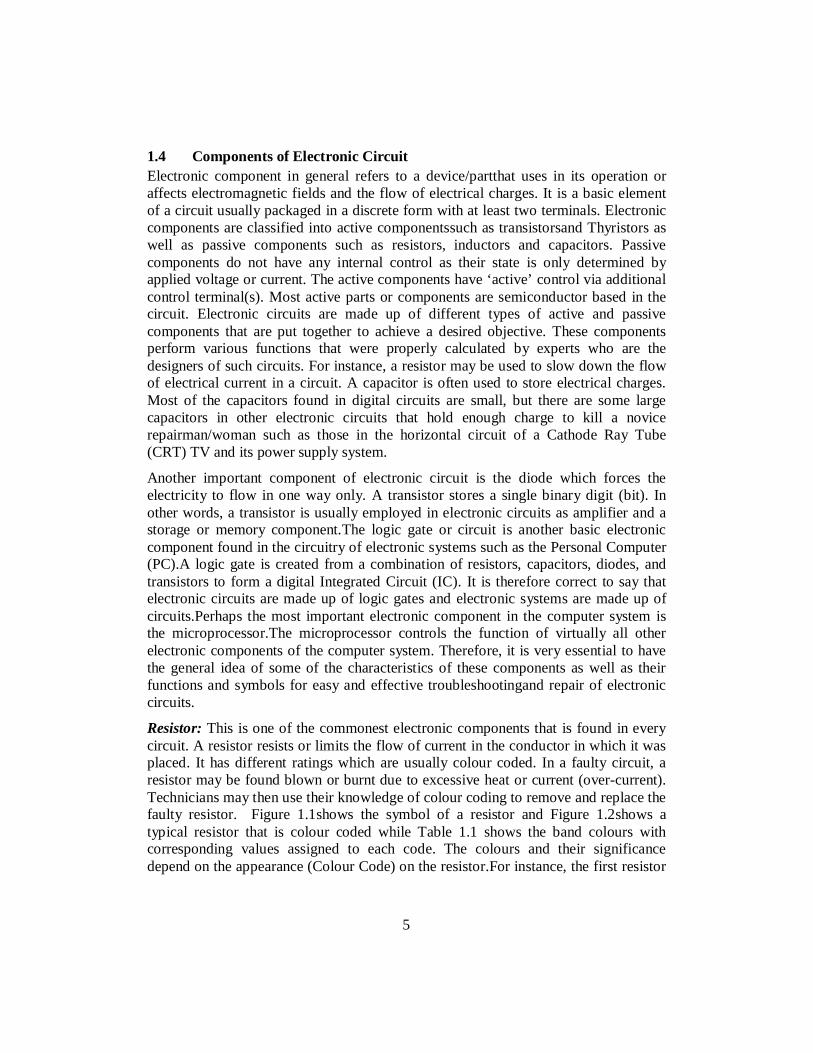
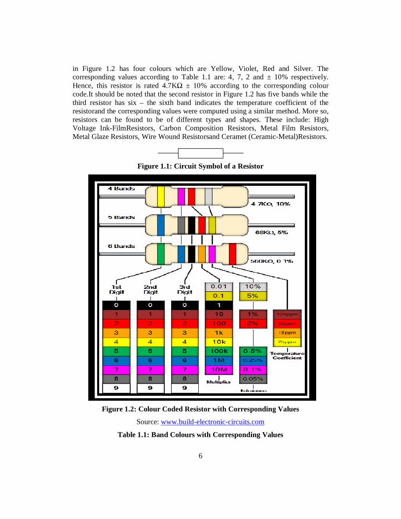
Resistor: This is one of the commonest electronic components that is found in every circuit. A resistor resists or limits the flow of current in the conductor in which it was placed. It has different ratings which are usually colour coded. In a faulty circuit, a resistor may be found blown or burnt due to excessive heat or current (over-current). Technicians may then use their knowledge of colour coding to remove and replace the faulty resistor. Figure 1.1shows the symbol of a resistor and Figure 1.2shows a typical resistor that is colour coded while Table 1.1 shows the band colours with corresponding values assigned to each code. The colours and their significance depend on the appearance (Colour Code) on the resistor.For instance, the first resistor
6
in Figure 1.2 has four colours which are Yellow, Violet, Red and Silver. The corresponding values according to Table 1.1 are: 4, 7, 2 and ± 10% respectively. Hence, this resistor is rated 4.7KΩ ± 10% according to the corresponding colour code.It should be noted that the second resistor in Figure 1.2 has five bands while the third resistor has six – the sixth band indicates the temperature coefficient of the resistorand the corresponding values were computed using a similar method. More so, resistors can be found to be of different types and shapes. These include: High Voltage Ink-FilmResistors, Carbon Composition Resistors, Metal Film Resistors, Metal Glaze Resistors, Wire Wound Resistorsand Ceramet (Ceramic-Metal)Resistors.
Figure 1.1: Circuit Symbol of a Resistor
Figure 1.2: Colour Coded Resistor with Corresponding Values
Source: www.build-electronic-circuits.com
Table 1.1: Band Colours with Corresponding Values
7
Band Colour Digit Multiplier Tolerance
Black 0 1 -
Brown 1 10 ± 1%
Red 2 100 ± 2%
Orange 3 1000 ± 3 %
Yellow 4 10,000 ± 4%
Green 5 100,000 -
Blue 6 1000,000 -
Violet 7 10,000,000 -
Grey 8 100,000,000 -
White 9 - -
Gold - 0.1 ± 5%
Silver - 0.01 ± 10%
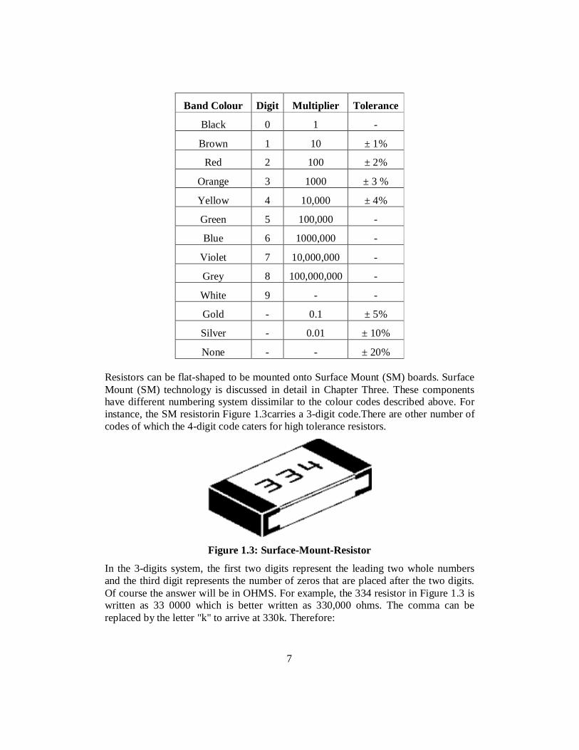
None - - ± 20% Resistors can be flat-shaped to be mounted onto Surface Mount (SM) boards. Surface Mount (SM) technology is discussed in detail in Chapter Three. These components have different numbering system dissimilar to the colour codes described above. For instance, the SM resistorin Figure 1.3carries a 3-digit code.There are other number of codes of which the 4-digit code caters for high tolerance resistors.
Figure 1.3: Surface-Mount-Resistor
In the 3-digits system, the first two digits represent the leading two whole numbers and the third digit represents the number of zeros that are placed after the two digits. Of course the answer will be in OHMS. For example, the 334 resistor in Figure 1.3 is written as 33 0000 which is better written as 330,000 ohms. The comma can be replaced by the letter "k" to arrive at 330k. Therefore:
8
222 = 22 00 = 2,200 = 2k2
473 = 47 000 = 47,000 = 47k
474 = 47 0000 = 470,000 = 470k
105 = 10 00000 = 1,000,000 = 1M = one million ohms
There is a trick one has to remember. Resistances less than 100 ohms are written as: 10 ohms = 10R or 22 and no zeros = 22R or 47 and no zeros = 47R. Sometimes the resistor is marked: 10, 22 and 47 to avoid confusion. Remember: R = ohms; k = kilo ohms = 1,000 ohms; M = Meg = 1,000,000 ohms. The 3 letters (R, k and M) are put in place of the decimal point. This way one cannot make a mistake when reading a value of resistance. There are also some new types of current sensing surface-mount resistors in electronic circuits that are rated in milli-ohms. A milli-ohm is one thousandth of an ohm and is written 0.001Ω when writing a normal mathematical number. When written on a surface mount resistor, the letter R indicates the decimal point and it also signifies the word "OHM" or "OHMS" and one milli-ohm is written R001 Five miili-ohms is R005 and one hundred milliohms is R100. Some surface mount resistors have the letter "M" after the value to indicate the resistor has a rating of 1 watt. e.g: R100M.
These surface-mount resistors are specially-made to withstand a high temperature and a surface-mount resistor of the same size is normally 250mW or less. These current-sensing resistors can get extremely hot and the PC board on which they are mounted can become burnt or damaged. This is why in PC boards, heat sinks are made very large to dissipate the heat. Normally a current sensing resistor is below one ohm (1R0) and it is easy to identify them as R100 etc. You cannot measure the value of a current sensing resistor as the leads of a multimeter have a higher resistance than the resistor and few multimeters can read values below one ohm. If the value is not visible, you will have to refer to the circuit. Before replacing it, think about why it failed.
Capacitors:A capacitor is an electronic component that stores electric charges. Hence the ability of a capacitor to store electric charges is called capacitance. Capacitors are basically made up of two metallic plates that are separated by an insulator called the dielectric. Like the resistors, capacitors too have different shapes and values of capacitance. These capacitors which can be found for different applications in electronic circuitsinclude: Electrolytic Capacitors, Motor-run Capacitors, Suppressor Capacitors, Tantalum Capacitors, Ceramic Capacitors, Polyester Capacitors, Memory Backup Capacitors, Polystyrene Capacitors and Trimmer Capacitors among others.
Electrolytic Capacitors: An electrolytic capacitor is a type of capacitor that uses an electrolyte to achieve a larger capacitance than other capacitor types. An electrolyte is a liquid or gel containing a high concentration of ions. Almost all electrolytic capacitors are polarized, which means that the voltage on the positive terminal must always be greater than the voltage on the negative terminal due to the construction of
9
the capacitors and the characteristics of the electrolyte used. If the capacitor becomes reverse-biased (if the voltage polarity on the terminals is reversed), the insulating aluminium oxide, which acts as a dielectric, might get damaged and start acting as a short circuit between the two capacitor terminals. This can cause the capacitor to overheat due to the large current running through it. As the capacitor overheats, the electrolyte heats up and leaks or even vaporizes, causing the enclosure to burst. This process happens at reverse voltages of about 1 volt and above. To maintain safety and prevent the enclosure from exploding due to high pressures generated under overheat conditions, a safety valve is installed in the enclosure. It is typically made by making a score in the upper face of the capacitor, which pops open in a controlled manner when the capacitor overheats. Since electrolytes may be toxic or corrosive, additional safety measures may need to be taken when cleaning after and replacing an overheated electrolytic capacitor.
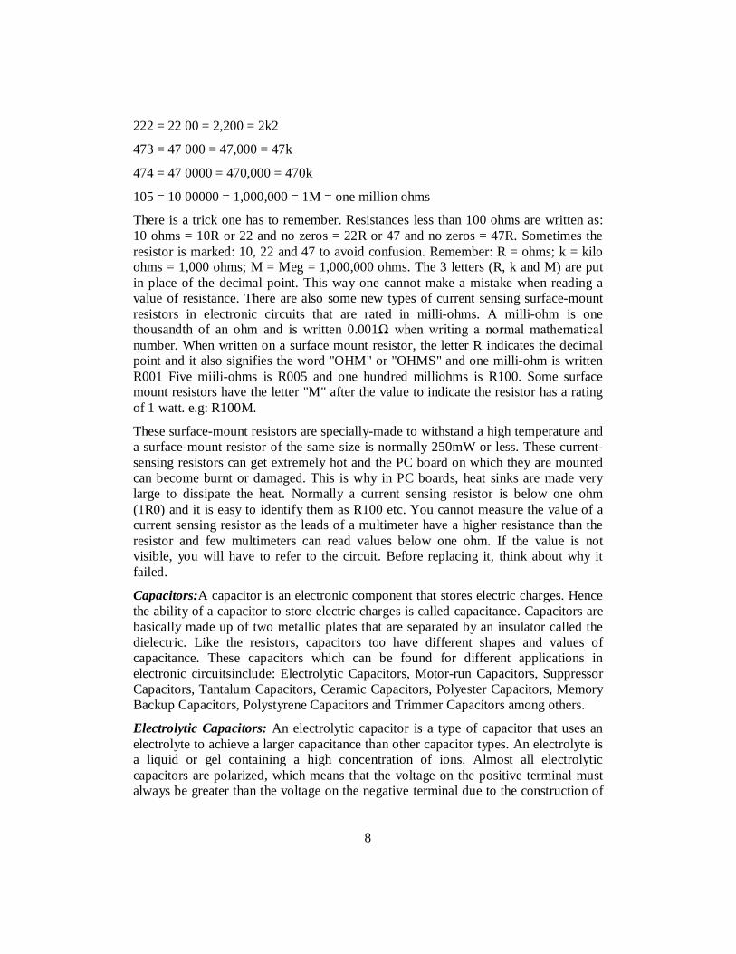
Therefore, the benefit of large capacitance in electrolytic capacitors comes with several drawbacks as well. Among these drawbacks are large leakage currents, value tolerances, equivalent series resistance and a limited lifetime. Most popular among electrolytic capacitors are AluminiumElectrolytic Capacitorswhich are found in many applications such as power supplies, computer motherboards and in many domestic appliances. Since they are polarized, they may be used only in DC circuits. Figure 1.4 shows the circuit symbol and different packages of electrolytic capacitors.
Electrolytic capacitors are commonly used as filtering devices in various power supplies to reduce the voltage ripple. When used in switching power supplies, they are often the critical component limiting the usable life of the power supply, so high quality capacitors are used in this application.These capacitors may also be used in input and output smoothing as a low pass filter if the signal is a DC signal with a weak AC component. However, electrolytic capacitors do not work well with large amplitude and high frequency signals due to the power dissipated at the parasitic internal resistance called equivalent series resistance (ESR). In such applications, low-
10
ESR capacitors must be used to reduce losses and avoid overheating.Another practical example is the use of electrolytic capacitors as filters in audio amplifiers whose main goal is to reduce mains hum. Mains hum is a 50Hz or 60Hz electrical noise induced from the mains supply which would be audible if amplified.
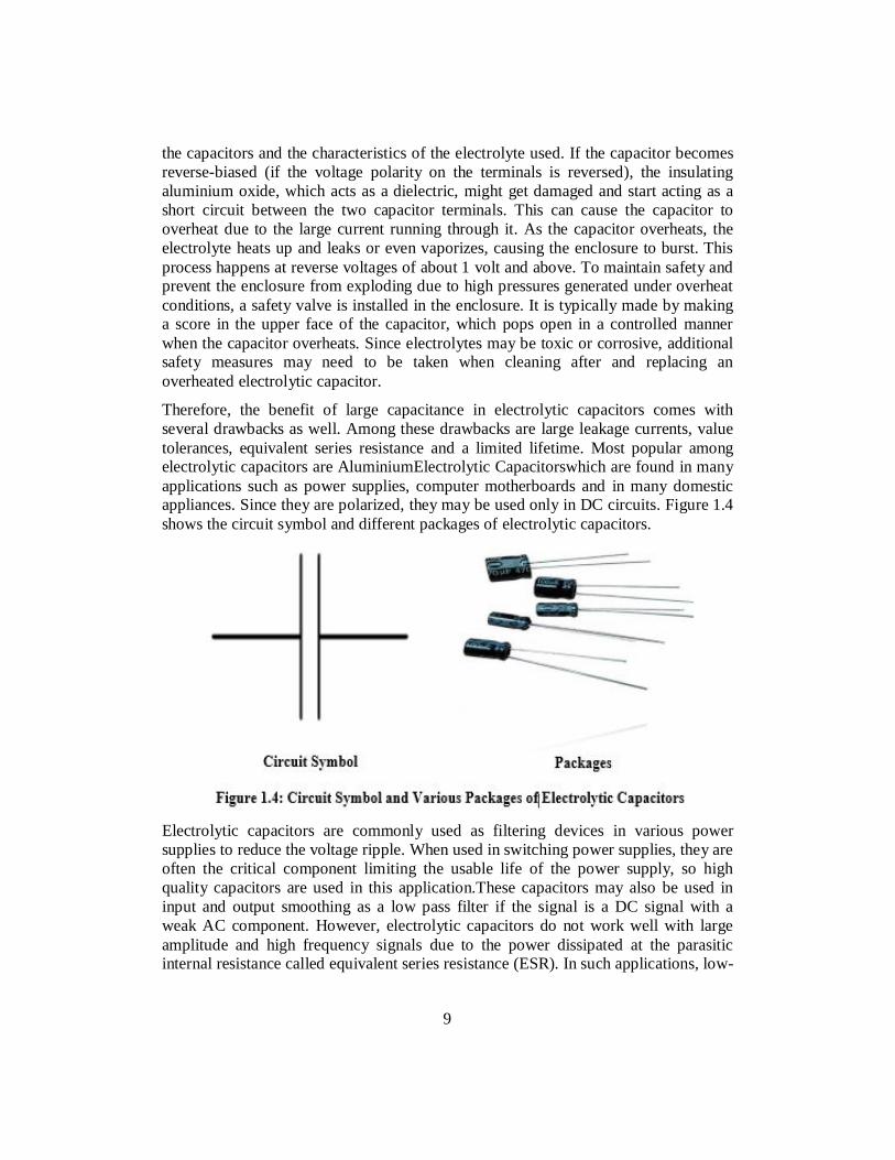
Motor Run Capacitors:Some single phase AC motor designs use Motor Run Capacitors also referred to as Run Capacitors, which are left connected to the auxiliary coil even after the start capacitor is disconnected by a centrifugal switch. These designs operate by creating a rotating magnetic field. Motor Run Capacitors are designed for continuous duty, and remain powered whenever the motor is powered, which is why electrolytic capacitors are avoided, and low-loss polymer capacitors are used instead. The capacitance of Run Capacitors is usually lower than the capacitance of start capacitors, and is often in the range of 1.5 µF to 100 µF. Choosing a wrong capacitance value for a motor can result in an uneven magnetic field, which can be observed as uneven motor rotation speed, especially under load. This can cause additional noise from the motor, performance drops and increased energy consumption, as well as additional heating, which can cause the motor to overheat. Figure 1.5 shows a typical Motor Run Capacitor. It should be noted that the circuit symbol in Figure 1.4 is the same for all types of capacitors except the variable capacitors where a line is drawn across the symbol to signify the function.
Figure 1.5: Different Shapes of Motor-Run Capacitors
Motor start and run capacitors are used in single-phase AC induction motors. Such motors are used whenever a single-phase power supply is more practical than a three-phase power supply, such as in domestic applianceslike the fan that is usually employed for cooling of DVDs, computers and other electronic appliances. Other applications which utilize start and run motor capacitors include power tools, washing machines, tumble dryers, dishwashers, vacuum cleaners, air conditioners and compressors.
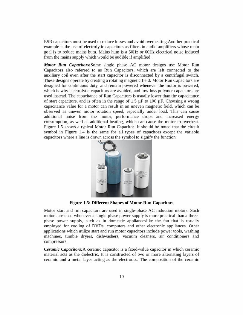
Ceramic Capacitors:A ceramic capacitor is a fixed-value capacitor in which ceramic material acts as the dielectric. It is constructed of two or more alternating layers of ceramic and a metal layer acting as the electrodes. The composition of the ceramic
11
material defines the electrical behaviour and therefore applications. Ceramic capacitors are used for all types of circuits in a number of applications which include: Coupling, decoupling, smoothing, and filtering of electric signals. Figure 1.6 shows through-hole and surface-mountedceramic capacitors in various shapes.
Figure 1.6: Through-Hole and Surface-Mounted Ceramic Capacitors
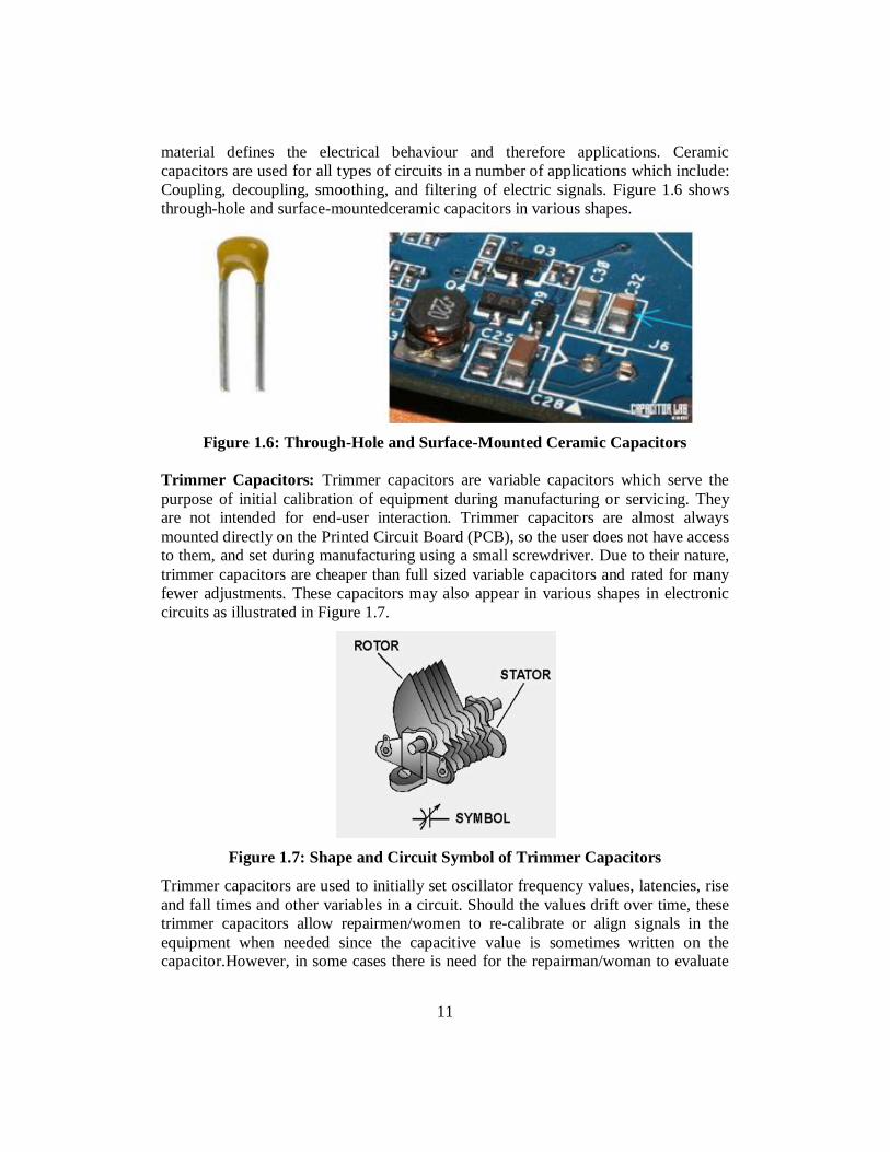
Trimmer Capacitors: Trimmer capacitors are variable capacitors which serve the purpose of initial calibration of equipment during manufacturing or servicing. They are not intended for end-user interaction. Trimmer capacitors are almost always mounted directly on the Printed Circuit Board (PCB), so the user does not have access to them, and set during manufacturing using a small screwdriver. Due to their nature, trimmer capacitors are cheaper than full sized variable capacitors and rated for many fewer adjustments. These capacitors may also appear in various shapes in electronic circuits as illustrated in Figure 1.7.
Figure 1.7: Shape and Circuit Symbol of Trimmer Capacitors
Trimmer capacitors are used to initially set oscillator frequency values, latencies, rise and fall times and other variables in a circuit. Should the values drift over time, these trimmer capacitors allow repairmen/women to re-calibrate or align signals in the equipment when needed since the capacitive value is sometimes written on the capacitor.However, in some cases there is need for the repairman/woman to evaluate
12
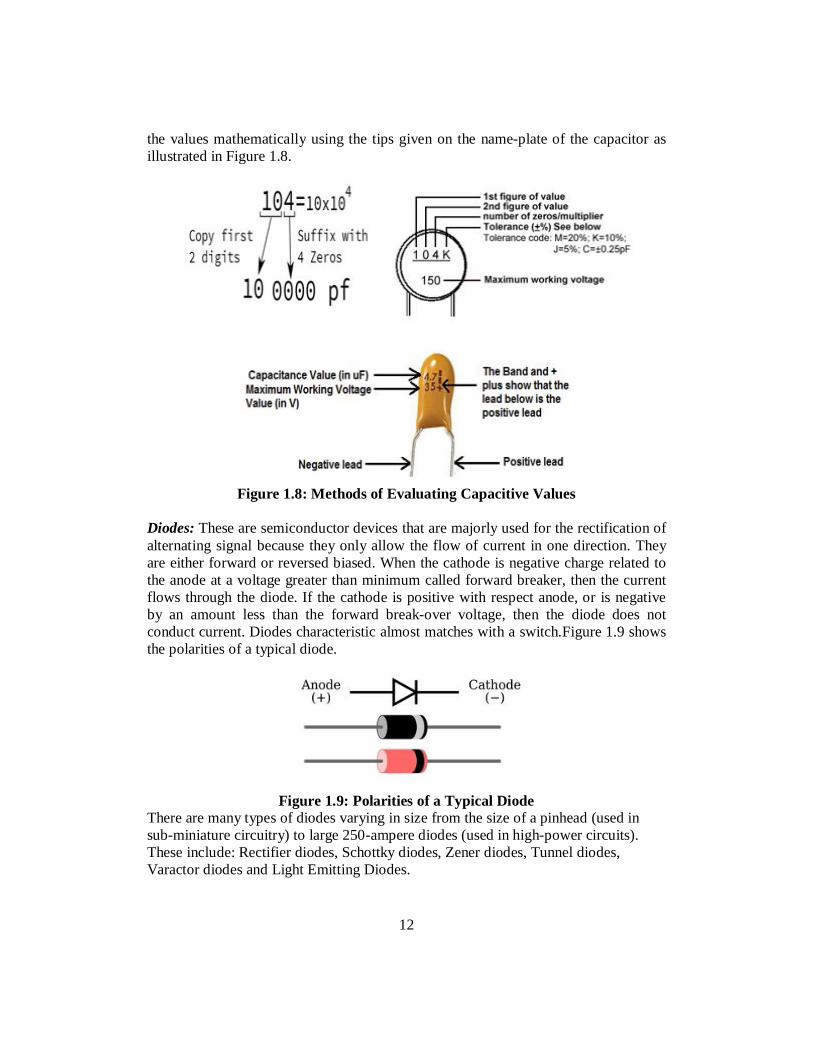
the values mathematically using the tips given on the name-plate of the capacitor as illustrated in Figure 1.8.
Figure 1.8: Methods of Evaluating Capacitive Values
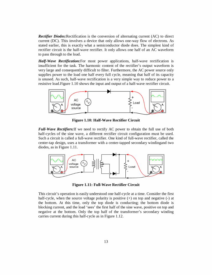
Diodes: These are semiconductor devices that are majorly used for the rectification of alternating signal because they only allow the flow of current in one direction. They are either forward or reversed biased. When the cathode is negative charge related to the anode at a voltage greater than minimum called forward breaker, then the current flows through the diode. If the cathode is positive with respect anode, or is negative by an amount less than the forward break-over voltage, then the diode does not conduct current. Diodes characteristic almost matches with a switch.Figure 1.9 shows the polarities of a typical diode.
Figure 1.9: Polarities of a Typical Diode
There are many types of diodes varying in size from the size of a pinhead (used in sub-miniature circuitry) to large 250-ampere diodes (used in high-power circuits). These include: Rectifier diodes, Schottky diodes, Zener diodes, Tunnel diodes, Varactor diodes and Light Emitting Diodes.
13
Rectifier Diodes:Rectification is the conversion of alternating current (AC) to direct current (DC). This involves a device that only allows one-way flow of electrons. As stated earlier, this is exactly what a semiconductor diode does. The simplest kind of rectifier circuit is the half-wave rectifier. It only allows one half of an AC waveform to pass through to the load.
Half-Wave Rectification:For most power applications, half-wave rectification is insufficient for the task. The harmonic content of the rectifier’s output waveform is very large and consequently difficult to filter. Furthermore, the AC power source only supplies power to the load one half every full cycle, meaning that half of its capacity is unused. As such, half-wave rectification is a very simple way to reduce power to a resistive load.Figure 1.10 shows the input and output of a half-wave rectifier circuit.
Figure 1.10: Half-Wave Rectifier Circuit
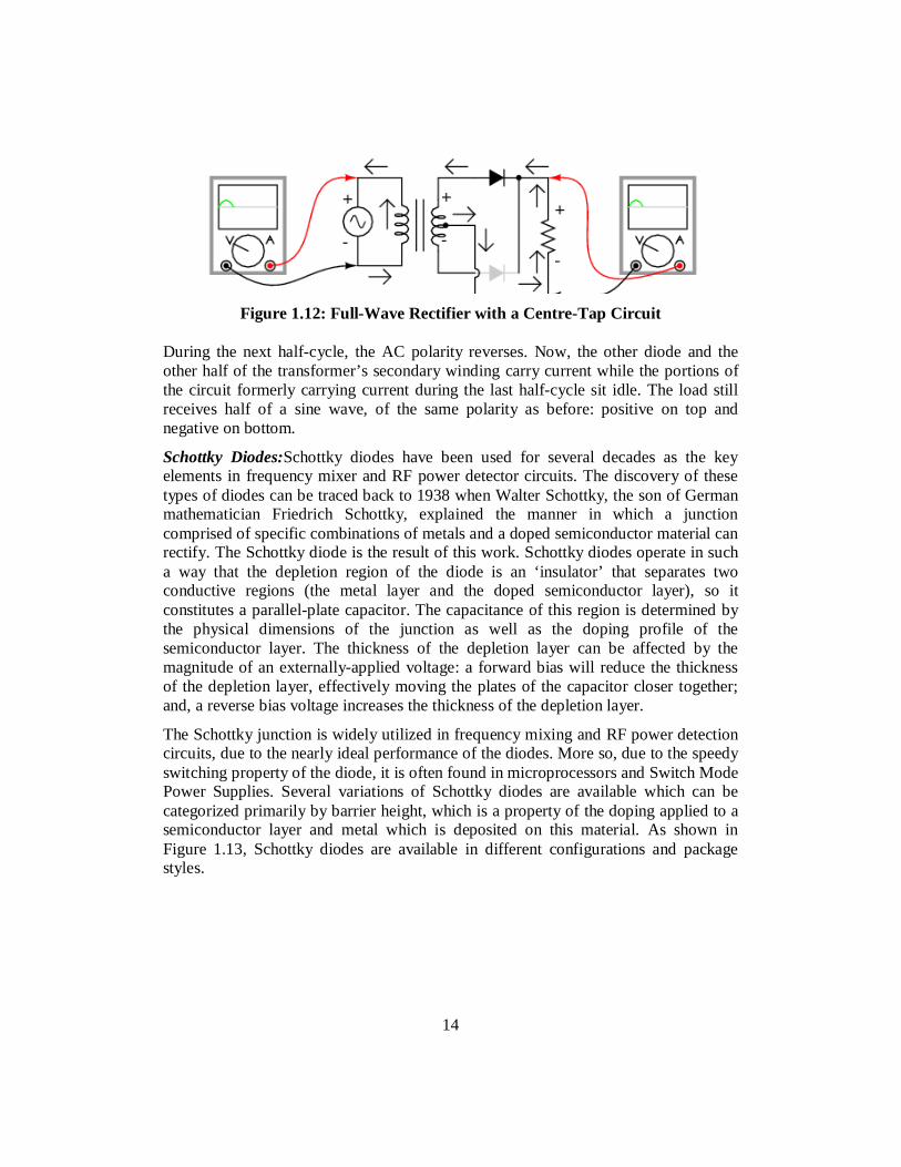
Full-Wave Rectifiers:If we need to rectify AC power to obtain the full use of both half-cycles of the sine wave, a different rectifier circuit configuration must be used. Such a circuit is called a full-wave rectifier. One kind of full-wave rectifier, called the center-tap design, uses a transformer with a center-tapped secondary windingand two diodes, as in Figure 1.11.
Figure 1.11: Full-Wave Rectifier Circuit
This circuit’s operation is easily understood one half-cycle at a time. Consider the first half-cycle, when the source voltage polarity is positive (+) on top and negative (-) at the bottom. At this time, only the top diode is conducting; the bottom diode is blocking current, and the load ‘sees’ the first half of the sine wave, positive on top and negative at the bottom. Only the top half of the transformer’s secondary winding carries current during this half-cycle as in Figure 1.12.
14
Figure 1.12: Full-Wave Rectifier with a Centre-Tap Circuit
During the next half-cycle, the AC polarity reverses. Now, the other diode and the other half of the transformer’s secondary winding carry current while the portions of the circuit formerly carrying current during the last half-cycle sit idle. The load still receives half of a sine wave, of the same polarity as before: positive on top and negative on bottom.
Schottky Diodes:Schottky diodes have been used for several decades as the key elements in frequency mixer and RF power detector circuits. The discovery of these types of diodes can be traced back to 1938 when Walter Schottky, the son of German mathematician Friedrich Schottky, explained the manner in which a junction comprised of specific combinations of metals and a doped semiconductor material can rectify. The Schottky diode is the result of this work. Schottky diodes operate in such a way that the depletion region of the diode is an ‘insulator’ that separates two conductive regions (the metal layer and the doped semiconductor layer), so it constitutes a parallel-plate capacitor. The capacitance of this region is determined by the physical dimensions of the junction as well as the doping profile of the semiconductor layer. The thickness of the depletion layer can be affected by the magnitude of an externally-applied voltage: a forward bias will reduce the thickness of the depletion layer, effectively moving the plates of the capacitor closer together; and, a reverse bias voltage increases the thickness of the depletion layer.
The Schottky junction is widely utilized in frequency mixing and RF power detection circuits, due to the nearly ideal performance of the diodes. More so, due to the speedy switching property of the diode, it is often found in microprocessors and Switch Mode Power Supplies. Several variations of Schottky diodes are available which can be categorized primarily by barrier height, which is a property of the doping applied to a semiconductor layer and metal which is deposited on this material. As shown in Figure 1.13, Schottky diodes are available in different configurations and package styles.
15
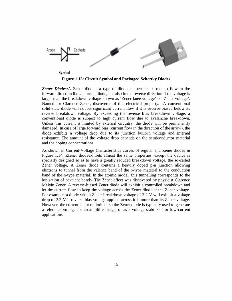
Figure 1.13: Circuit Symbol and Packaged Schottky Diodes
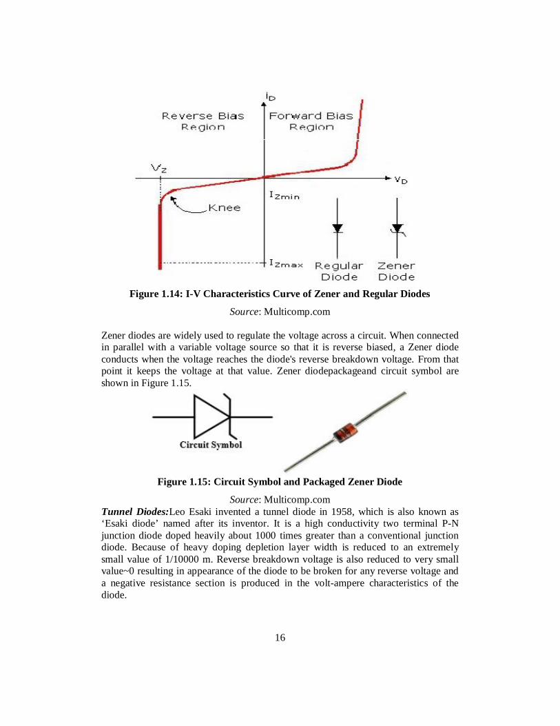
Zener Diodes:A Zener diodeis a type of diodethat permits current to flow in the forward direction like a normal diode, but also in the reverse direction if the voltage is larger than the breakdown voltage known as ‘Zener knee voltage’ or ‘Zener voltage’. Named for Clarence Zener, discoverer of this electrical property. A conventional solid-state diode will not let significant current flow if it is reverse-biased below its reverse breakdown voltage. By exceeding the reverse bias breakdown voltage, a conventional diode is subject to high current flow due to avalanche breakdown. Unless this current is limited by external circuitry, the diode will be permanently damaged. In case of large forward bias (current flow in the direction of the arrow), the diode exhibits a voltage drop due to its junction built-in voltage and internal resistance. The amount of the voltage drop depends on the semiconductor material and the doping concentrations.
As shown in Current-Voltage Characteristics curves of regular and Zener diodes in Figure 1.14, aZener diodeexhibits almost the same properties, except the device is specially designed so as to have a greatly reduced breakdown voltage, the so-called Zener voltage. A Zener diode contains a heavily doped p-n junction allowing electrons to tunnel from the valence band of the p-type material to the conduction band of the n-type material. In the atomic model, this tunnelling corresponds to the ionization of covalent bonds. The Zener effect was discovered by physicist Clarence Melvin Zener. A reverse-biased Zener diode will exhibit a controlled breakdown and let the current flow to keep the voltage across the Zener diode at the Zener voltage. For example, a diode with a Zener breakdown voltage of 3.2 V will exhibit a voltage drop of 3.2 V if reverse bias voltage applied across it is more than its Zener voltage. However, the current is not unlimited, so the Zener diode is typically used to generate a reference voltage for an amplifier stage, or as a voltage stabilizer for low-current applications.
16
Figure 1.14: I-V Characteristics Curve of Zener and Regular Diodes
Source: Multicomp.com Zener diodes are widely used to regulate the voltage across a circuit. When connected in parallel with a variable voltage source so that it is reverse biased, a Zener diode conducts when the voltage reaches the diode's reverse breakdown voltage. From that point it keeps the voltage at that value. Zener diodepackageand circuit symbol are shown in Figure 1.15.
Figure 1.15: Circuit Symbol and Packaged Zener Diode
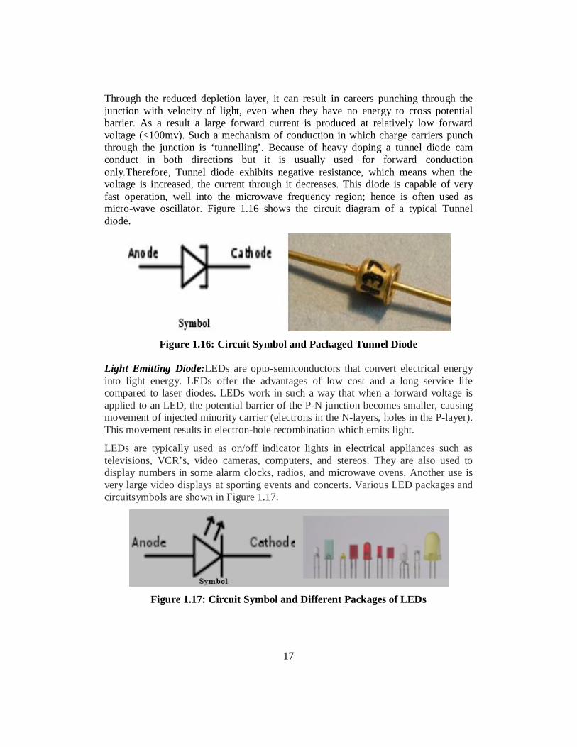
Source: Multicomp.com Tunnel Diodes:Leo Esaki invented a tunnel diode in 1958, which is also known as ‘Esaki diode’ named after its inventor. It is a high conductivity two terminal P-N junction diode doped heavily about 1000 times greater than a conventional junction diode. Because of heavy doping depletion layer width is reduced to an extremely small value of 1/10000 m. Reverse breakdown voltage is also reduced to very small value~0 resulting in appearance of the diode to be broken for any reverse voltage and a negative resistance section is produced in the volt-ampere characteristics of the diode.
17
Through the reduced depletion layer, it can result in careers punching through the junction with velocity of light, even when they have no energy to cross potential barrier. As a result a large forward current is produced at relatively low forward voltage (<100mv). Such a mechanism of conduction in which charge carriers punch through the junction is ‘tunnelling’. Because of heavy doping a tunnel diode cam conduct in both directions but it is usually used for forward conduction only.Therefore, Tunnel diode exhibits negative resistance, which means when the voltage is increased, the current through it decreases. This diode is capable of very fast operation, well into the microwave frequency region; hence is often used as micro-wave oscillator. Figure 1.16 shows the circuit diagram of a typical Tunnel diode.
Figure 1.16: Circuit Symbol and Packaged Tunnel Diode
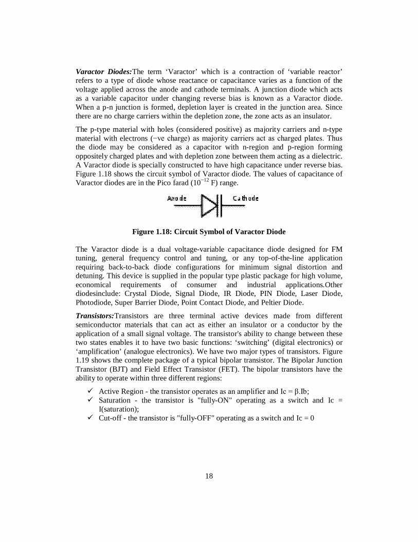
Light Emitting Diode:LEDs are opto-semiconductors that convert electrical energy into light energy. LEDs offer the advantages of low cost and a long service life compared to laser diodes. LEDs work in such a way that when a forward voltage is applied to an LED, the potential barrier of the P-N junction becomes smaller, causing movement of injected minority carrier (electrons in the N-layers, holes in the P-layer). This movement results in electron-hole recombination which emits light.
LEDs are typically used as on/off indicator lights in electrical appliances such as televisions, VCR’s, video cameras, computers, and stereos. They are also used to display numbers in some alarm clocks, radios, and microwave ovens. Another use is very large video displays at sporting events and concerts. Various LED packages and circuitsymbols are shown in Figure 1.17.
Figure 1.17: Circuit Symbol and Different Packages of LEDs
18
Varactor Diodes:The term ‘Varactor’ which is a contraction of ‘variable reactor’ refers to a type of diode whose reactance or capacitance varies as a function of the voltage applied across the anode and cathode terminals. A junction diode which acts as a variable capacitor under changing reverse bias is known as a Varactor diode. When a p-n junction is formed, depletion layer is created in the junction area. Since there are no charge carriers within the depletion zone, the zone acts as an insulator.
The p-type material with holes (considered positive) as majority carriers and n-type material with electrons (−ve charge) as majority carriers act as charged plates. Thus the diode may be considered as a capacitor with n-region and p-region forming oppositely charged plates and with depletion zone between them acting as a dielectric. A Varactor diode is specially constructed to have high capacitance under reverse bias. Figure 1.18 shows the circuit symbol of Varactor diode. The values of capacitance of Varactor diodes are in the Pico farad (10−12 F) range.
Figure 1.18: Circuit Symbol of Varactor Diode
The Varactor diode is a dual voltage-variable capacitance diode designed for FM tuning, general frequency control and tuning, or any top-of-the-line application requiring back-to-back diode configurations for minimum signal distortion and detuning. This device is supplied in the popular type plastic package for high volume, economical requirements of consumer and industrial applications.Other diodesinclude: Crystal Diode, Signal Diode, IR Diode, PIN Diode, Laser Diode, Photodiode, Super Barrier Diode, Point Contact Diode, and Peltier Diode.
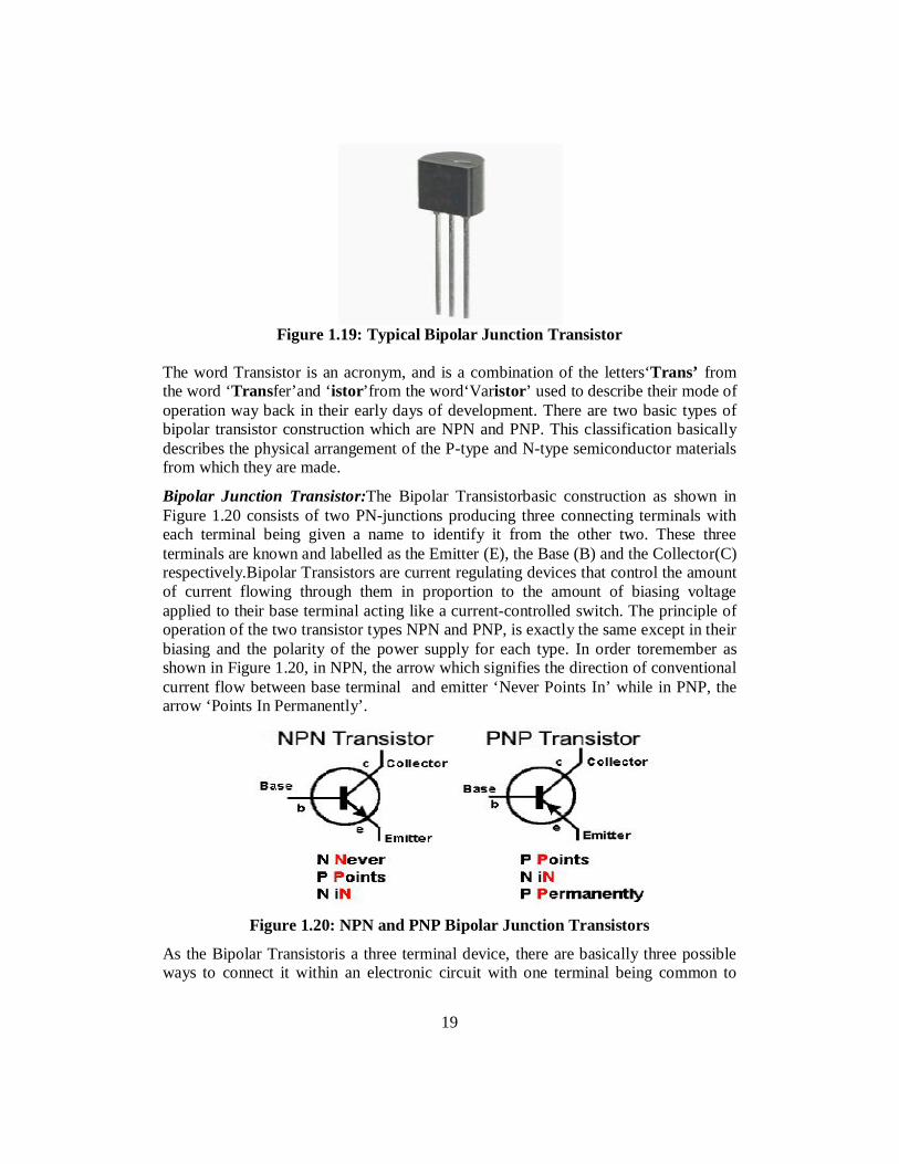
Transistors:Transistors are three terminal active devices made from different semiconductor materials that can act as either an insulator or a conductor by the application of a small signal voltage. The transistor's ability to change between these two states enables it to have two basic functions: ‘switching’ (digital electronics) or ‘amplification’ (analogue electronics). We have two major types of transistors. Figure 1.19 shows the complete package of a typical bipolar transistor. The Bipolar Junction Transistor (BJT) and Field Effect Transistor (FET). The bipolar transistors have the ability to operate within three different regions:
Active Region - the transistor operates as an amplifier and Ic = β.Ib; Saturation - the transistor is "fully-ON" operating as a switch and Ic =
I(saturation); Cut-off - the transistor is "fully-OFF" operating as a switch and Ic = 0
19
Figure 1.19: Typical Bipolar Junction Transistor
The word Transistor is an acronym, and is a combination of the letters‘Trans’ from the word ‘Transfer’and ‘istor’from the word‘Varistor’ used to describe their mode of operation way back in their early days of development. There are two basic types of bipolar transistor construction which are NPN and PNP. This classification basically describes the physical arrangement of the P-type and N-type semiconductor materials from which they are made.
Bipolar Junction Transistor:The Bipolar Transistorbasic construction as shown in Figure 1.20 consists of two PN-junctions producing three connecting terminals with each terminal being given a name to identify it from the other two. These three terminals are known and labelled as the Emitter (E), the Base (B) and the Collector(C) respectively.Bipolar Transistors are current regulating devices that control the amount of current flowing through them in proportion to the amount of biasing voltage applied to their base terminal acting like a current-controlled switch. The principle of operation of the two transistor types NPN and PNP, is exactly the same except in their biasing and the polarity of the power supply for each type. In order toremember as shown in Figure 1.20, in NPN, the arrow which signifies the direction of conventional current flow between base terminal and emitter ‘Never Points In’ while in PNP, the arrow ‘Points In Permanently’.
Figure 1.20: NPN and PNP Bipolar Junction Transistors
As the Bipolar Transistoris a three terminal device, there are basically three possible ways to connect it within an electronic circuit with one terminal being common to
20
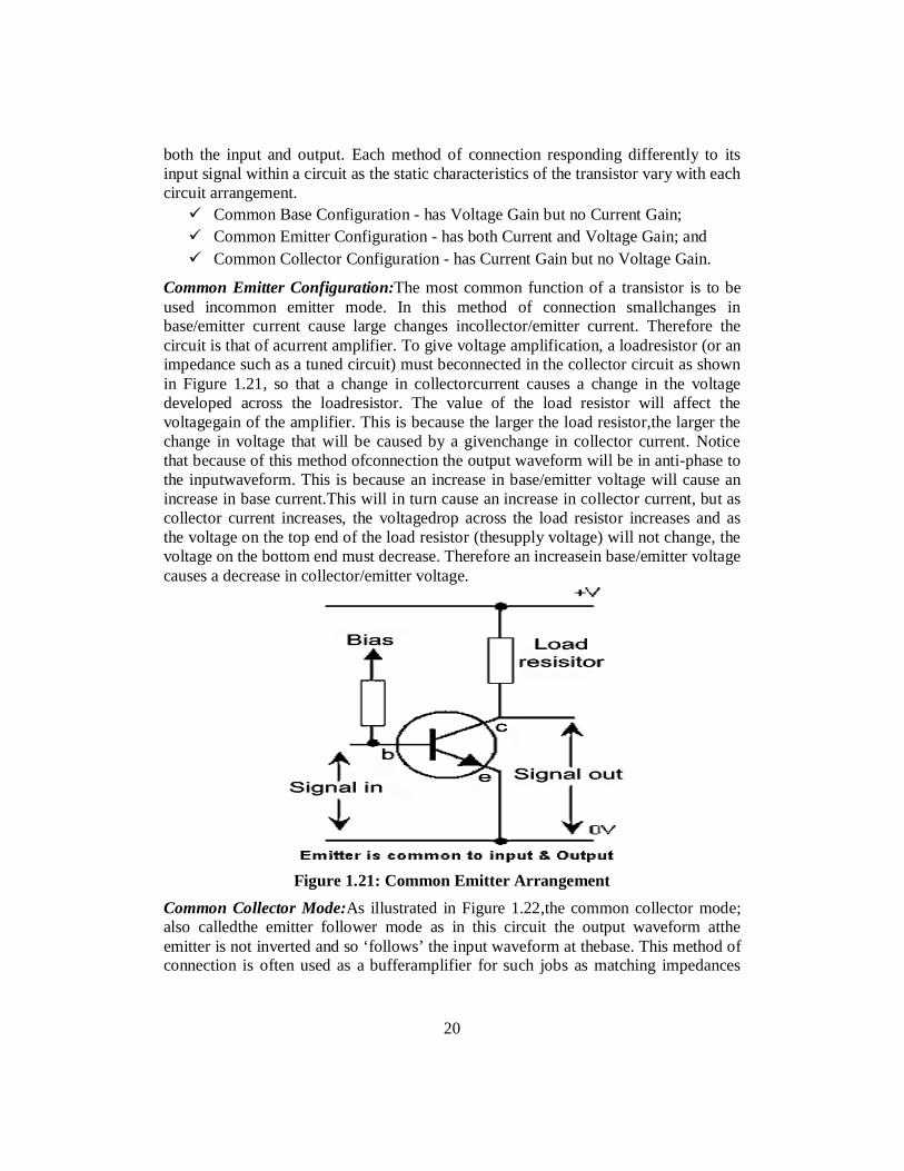
both the input and output. Each method of connection responding differently to its input signal within a circuit as the static characteristics of the transistor vary with each circuit arrangement. Common Base Configuration - has Voltage Gain but no Current Gain; Common Emitter Configuration - has both Current and Voltage Gain; and Common Collector Configuration - has Current Gain but no Voltage Gain.
Common Emitter Configuration:The most common function of a transistor is to be used incommon emitter mode. In this method of connection smallchanges in base/emitter current cause large changes incollector/emitter current. Therefore the circuit is that of acurrent amplifier. To give voltage amplification, a loadresistor (or an impedance such as a tuned circuit) must beconnected in the collector circuit as shown in Figure 1.21, so that a change in collectorcurrent causes a change in the voltage developed across the loadresistor. The value of the load resistor will affect the voltagegain of the amplifier. This is because the larger the load resistor,the larger the change in voltage that will be caused by a givenchange in collector current. Notice that because of this method ofconnection the output waveform will be in anti-phase to the inputwaveform. This is because an increase in base/emitter voltage will cause an increase in base current.This will in turn cause an increase in collector current, but as collector current increases, the voltagedrop across the load resistor increases and as the voltage on the top end of the load resistor (thesupply voltage) will not change, the voltage on the bottom end must decrease. Therefore an increasein base/emitter voltage causes a decrease in collector/emitter voltage.
Figure 1.21: Common Emitter Arrangement
Common Collector Mode:As illustrated in Figure 1.22,the common collector mode; also calledthe emitter follower mode as in this circuit the output waveform atthe emitter is not inverted and so ‘follows’ the input waveform at thebase. This method of connection is often used as a bufferamplifier for such jobs as matching impedances
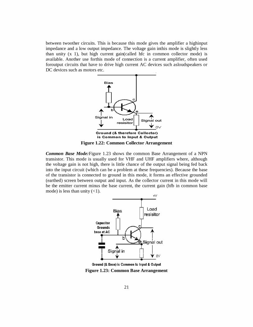
21
between twoother circuits. This is because this mode gives the amplifier a highinput impedance and a low output impedance. The voltage gain inthis mode is slightly less than unity (x 1), but high current gain(called hfc in common collector mode) is available. Another use forthis mode of connection is a current amplifier, often used foroutput circuits that have to drive high current AC devices such asloudspeakers or DC devices such as motors etc.
Figure 1.22: Common Collector Arrangement
Common Base Mode:Figure 1.23 shows the common Base Arrangement of a NPN transistor. This mode is usually used for VHF and UHF amplifiers where, although the voltage gain is not high, there is little chance of the output signal being fed back into the input circuit (which can be a problem at these frequencies). Because the base of the transistor is connected to ground in this mode, it forms an effective grounded (earthed) screen between output and input. As the collector current in this mode will be the emitter current minus the base current, the current gain (hfb in common base mode) is less than unity (<1).
Figure 1.23: Common Base Arrangement
22
Field Effect Transistor:There are two types of field-effect transistors, the Junction Field-Effect Transistor (JFET) and the ‘Metal-Oxide Semiconductor’ Field-Effect Transistor (MOSFET), or Insulated-Gate Field-Effect Transistor (IGFET). The principles on which these devices operate (current controlled by an electric field) are very similar — the primary difference being in the methods by which the control element is made. This difference, however, results in a considerable difference in device characteristics and necessitates variances in circuit design.
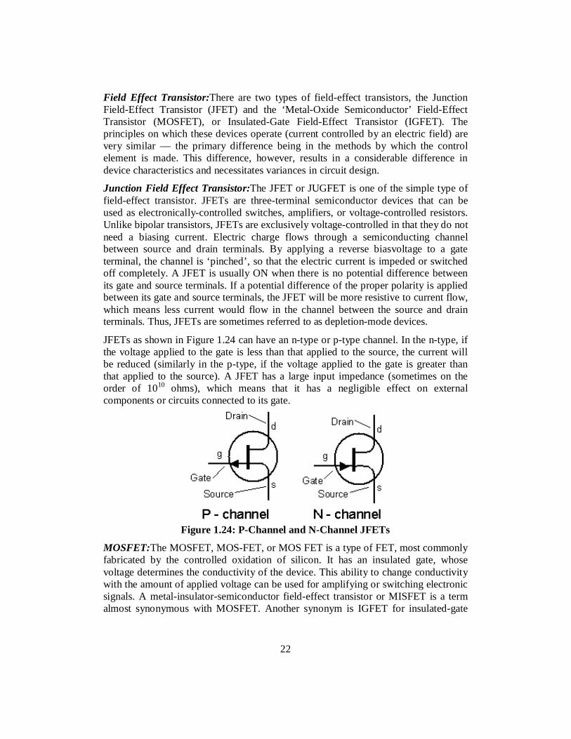
Junction Field Effect Transistor:The JFET or JUGFET is one of the simple type of field-effect transistor. JFETs are three-terminal semiconductor devices that can be used as electronically-controlled switches, amplifiers, or voltage-controlled resistors. Unlike bipolar transistors, JFETs are exclusively voltage-controlled in that they do not need a biasing current. Electric charge flows through a semiconducting channel between source and drain terminals. By applying a reverse biasvoltage to a gate terminal, the channel is ‘pinched’, so that the electric current is impeded or switched off completely. A JFET is usually ON when there is no potential difference between its gate and source terminals. If a potential difference of the proper polarity is applied between its gate and source terminals, the JFET will be more resistive to current flow, which means less current would flow in the channel between the source and drain terminals. Thus, JFETs are sometimes referred to as depletion-mode devices.
JFETs as shown in Figure 1.24 can have an n-type or p-type channel. In the n-type, if the voltage applied to the gate is less than that applied to the source, the current will be reduced (similarly in the p-type, if the voltage applied to the gate is greater than that applied to the source). A JFET has a large input impedance (sometimes on the order of 1010 ohms), which means that it has a negligible effect on external components or circuits connected to its gate.
Figure 1.24: P-Channel and N-Channel JFETs
MOSFET:The MOSFET, MOS-FET, or MOS FET is a type of FET, most commonly fabricated by the controlled oxidation of silicon. It has an insulated gate, whose voltage determines the conductivity of the device. This ability to change conductivity with the amount of applied voltage can be used for amplifying or switching electronic signals. A metal-insulator-semiconductor field-effect transistor or MISFET is a term almost synonymous with MOSFET. Another synonym is IGFET for insulated-gate
23
field-effect transistor. The main advantage of a MOSFET is that it requires almost no input current to control the load current, when compared with bipolar transistors. In an enhancement mode MOSFET, voltage applied to the gate terminal increases the conductivity of the device. In depletion mode transistors, voltage applied at the gate reduces the conductivity.
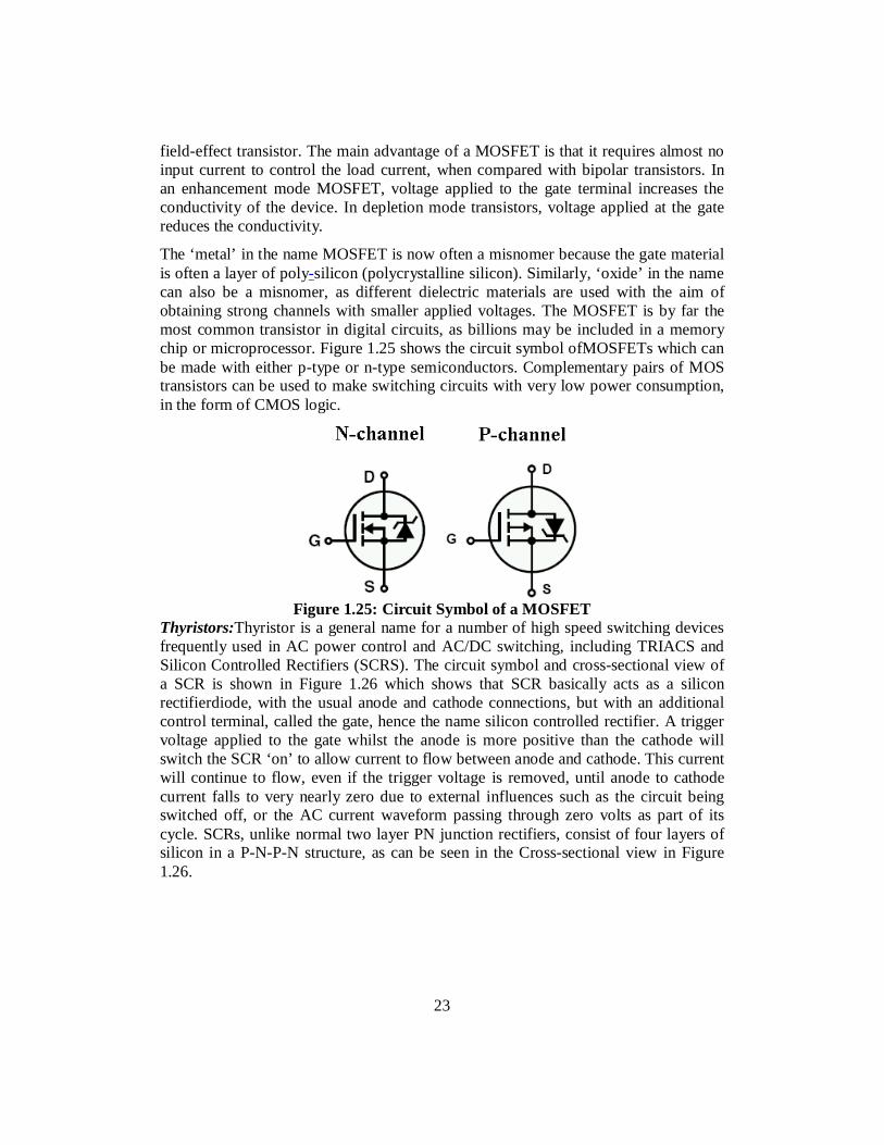
The ‘metal’ in the name MOSFET is now often a misnomer because the gate material is often a layer of poly-silicon (polycrystalline silicon). Similarly, ‘oxide’ in the name can also be a misnomer, as different dielectric materials are used with the aim of obtaining strong channels with smaller applied voltages. The MOSFET is by far the most common transistor in digital circuits, as billions may be included in a memory chip or microprocessor. Figure 1.25 shows the circuit symbol ofMOSFETs which can be made with either p-type or n-type semiconductors. Complementary pairs of MOS transistors can be used to make switching circuits with very low power consumption, in the form of CMOS logic.
Figure 1.25: Circuit Symbol of a MOSFET
Thyristors:Thyristor is a general name for a number of high speed switching devices frequently used in AC power control and AC/DC switching, including TRIACS and Silicon Controlled Rectifiers (SCRS). The circuit symbol and cross-sectional view of a SCR is shown in Figure 1.26 which shows that SCR basically acts as a silicon rectifierdiode, with the usual anode and cathode connections, but with an additional control terminal, called the gate, hence the name silicon controlled rectifier. A trigger voltage applied to the gate whilst the anode is more positive than the cathode will switch the SCR ‘on’ to allow current to flow between anode and cathode. This current will continue to flow, even if the trigger voltage is removed, until anode to cathode current falls to very nearly zero due to external influences such as the circuit being switched off, or the AC current waveform passing through zero volts as part of its cycle. SCRs, unlike normal two layer PN junction rectifiers, consist of four layers of silicon in a P-N-P-N structure, as can be seen in the Cross-sectional view in Figure 1.26.
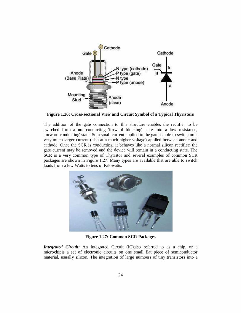
24
Figure 1.26: Cross-sectional View and Circuit Symbol of a Typical Thyristors
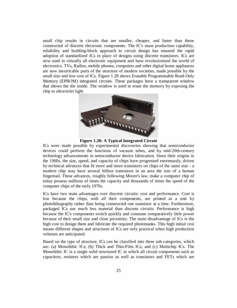
The addition of the gate connection to this structure enables the rectifier to be switched from a non-conducting 'forward blocking' state into a low resistance, 'forward conducting' state. So a small current applied to the gate is able to switch on a very much larger current (also at a much higher voltage) applied between anode and cathode. Once the SCR is conducting, it behaves like a normal silicon rectifier; the gate current may be removed and the device will remain in a conducting state. The SCR is a very common type of Thyristor and several examples of common SCR packages are shown in Figure 1.27. Many types are available that are able to switch loads from a few Watts to tens of Kilowatts.
Figure 1.27: Common SCR Packages
Integrated Circuit: An Integrated Circuit (IC)also referred to as a chip, or a microchipis a set of electronic circuits on one small flat piece of semiconductor material, usually silicon. The integration of large numbers of tiny transistors into a
25
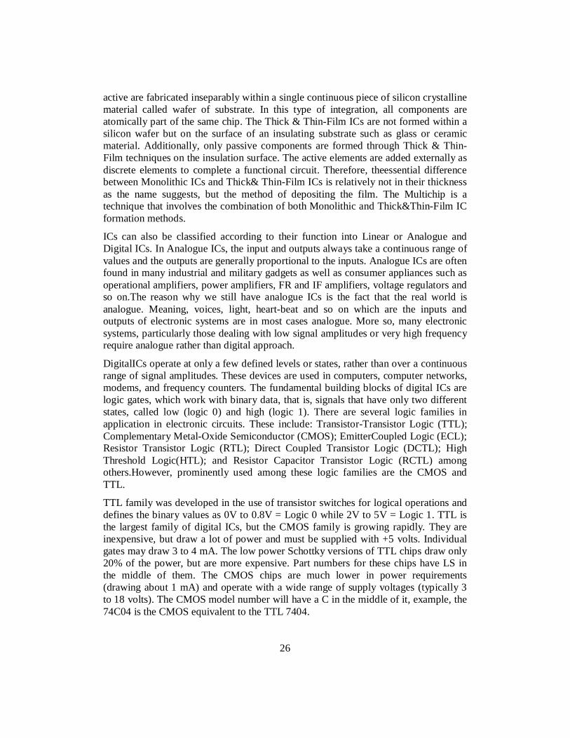
small chip results in circuits that are smaller, cheaper, and faster than those constructed of discrete electronic components. The IC's mass production capability, reliability and building-block approach to circuit design has ensured the rapid adoption of standardized ICs in place of designs using discrete transistors. ICs are now used in virtually all electronic equipment and have revolutionized the world of electronics. TVs, Radios, mobile phones, computers and other digital home appliances are now inextricable parts of the structure of modern societies, made possible by the small size and low cost of ICs. Figure 1.28 shows Erasable Programmable Read-Only Memory (EPROM) integrated circuits. These packages have a transparent window that shows the die inside. The window is used to erase the memory by exposing the chip to ultraviolet light.
Figure 1.28: A Typical Integrated Circuit
ICs were made possible by experimental discoveries showing that semiconductor devices could perform the functions of vacuum tubes, and by mid-20th-century technology advancements in semiconductor device fabrication. Since their origins in the 1960s, the size, speed, and capacity of chips have progressed enormously, driven by technical advances that fit more and more transistors on chips of the same size - a modern chip may have several billion transistors in an area the size of a human fingernail. These advances, roughly following Moore's law, make a computer chip of today possess millions of times the capacity and thousands of times the speed of the computer chips of the early 1970s.
ICs have two main advantages over discrete circuits: cost and performance. Cost is low because the chips, with all their components, are printed as a unit by photolithography rather than being constructed one transistor at a time. Furthermore, packaged ICs use much less material than discrete circuits. Performance is high because the IC's components switch quickly and consume comparatively little power because of their small size and close proximity. The main disadvantage of ICs is the high cost to design them and fabricate the required photomasks. This high initial cost means different shapes and structures of ICs are only practical when high production volumes are anticipated.
Based on the type of structure, ICs can be classified into three sub-categories, which are: (a) Monolithic ICs; (b) Thick and Thin-Film ICs; and (c) Multichip ICs. The Monolithic IC is a single solid structured IC in which all circuit components such as capacitors, resistors which are passive as well as transistors and FETs which are
26
active are fabricated inseparably within a single continuous piece of silicon crystalline material called wafer of substrate. In this type of integration, all components are atomically part of the same chip. The Thick & Thin-Film ICs are not formed within a silicon wafer but on the surface of an insulating substrate such as glass or ceramic material. Additionally, only passive components are formed through Thick & Thin-Film techniques on the insulation surface. The active elements are added externally as discrete elements to complete a functional circuit. Therefore, theessential difference between Monolithic ICs and Thick& Thin-Film ICs is relatively not in their thickness as the name suggests, but the method of depositing the film. The Multichip is a technique that involves the combination of both Monolithic and Thick&Thin-Film IC formation methods.
ICs can also be classified according to their function into Linear or Analogue and Digital ICs. In Analogue ICs, the input and outputs always take a continuous range of values and the outputs are generally proportional to the inputs. Analogue ICs are often found in many industrial and military gadgets as well as consumer appliances such as operational amplifiers, power amplifiers, FR and IF amplifiers, voltage regulators and so on.The reason why we still have analogue ICs is the fact that the real world is analogue. Meaning, voices, light, heart-beat and so on which are the inputs and outputs of electronic systems are in most cases analogue. More so, many electronic systems, particularly those dealing with low signal amplitudes or very high frequency require analogue rather than digital approach.
DigitalICs operate at only a few defined levels or states, rather than over a continuous range of signal amplitudes. These devices are used in computers, computer networks, modems, and frequency counters. The fundamental building blocks of digital ICs are logic gates, which work with binary data, that is, signals that have only two different states, called low (logic 0) and high (logic 1). There are several logic families in application in electronic circuits. These include: Transistor-Transistor Logic (TTL); Complementary Metal-Oxide Semiconductor (CMOS); EmitterCoupled Logic (ECL); Resistor Transistor Logic (RTL); Direct Coupled Transistor Logic (DCTL); High Threshold Logic(HTL); and Resistor Capacitor Transistor Logic (RCTL) among others.However, prominently used among these logic families are the CMOS and TTL.
TTL family was developed in the use of transistor switches for logical operations and defines the binary values as 0V to 0.8V = Logic 0 while 2V to 5V = Logic 1. TTL is the largest family of digital ICs, but the CMOS family is growing rapidly. They are inexpensive, but draw a lot of power and must be supplied with +5 volts. Individual gates may draw 3 to 4 mA. The low power Schottky versions of TTL chips draw only 20% of the power, but are more expensive. Part numbers for these chips have LS in the middle of them. The CMOS chips are much lower in power requirements (drawing about 1 mA) and operate with a wide range of supply voltages (typically 3 to 18 volts). The CMOS model number will have a C in the middle of it, example, the 74C04 is the CMOS equivalent to the TTL 7404.
27
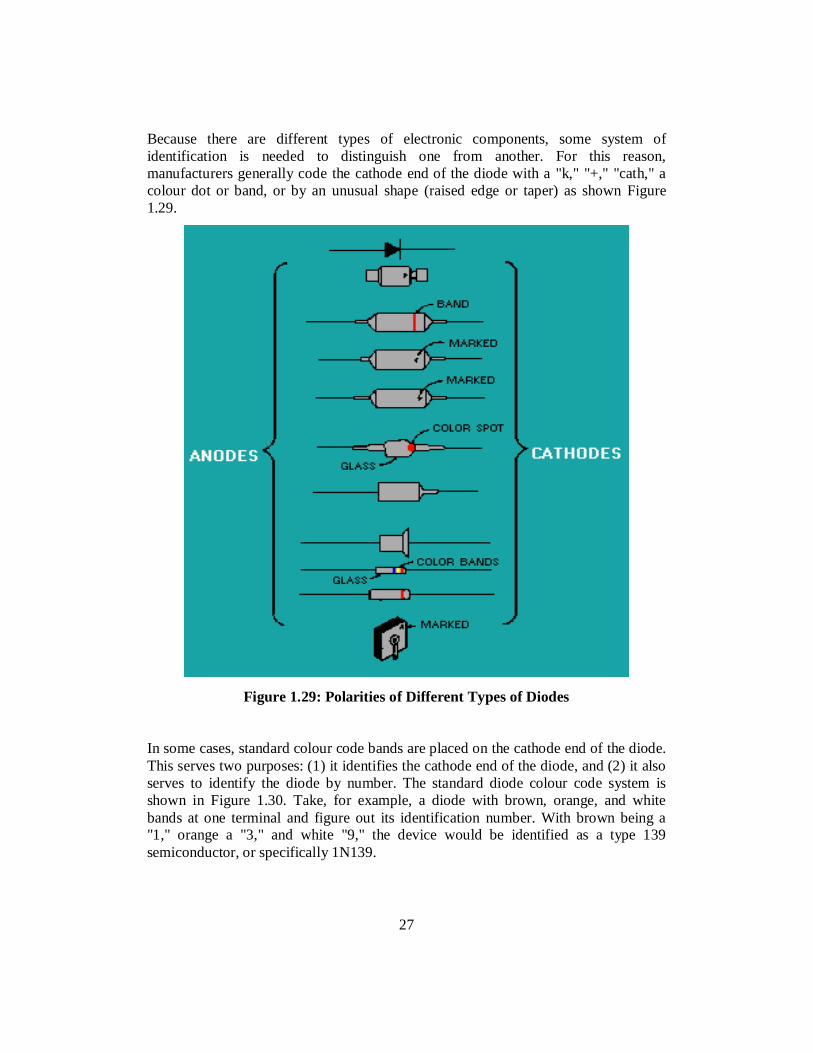
Because there are different types of electronic components, some system of identification is needed to distinguish one from another. For this reason, manufacturers generally code the cathode end of the diode with a "k," "+," "cath," a colour dot or band, or by an unusual shape (raised edge or taper) as shown Figure 1.29.
Figure 1.29: Polarities of Different Types of Diodes
In some cases, standard colour code bands are placed on the cathode end of the diode. This serves two purposes: (1) it identifies the cathode end of the diode, and (2) it also serves to identify the diode by number. The standard diode colour code system is shown in Figure 1.30. Take, for example, a diode with brown, orange, and white bands at one terminal and figure out its identification number. With brown being a "1," orange a "3," and white "9," the device would be identified as a type 139 semiconductor, or specifically 1N139.
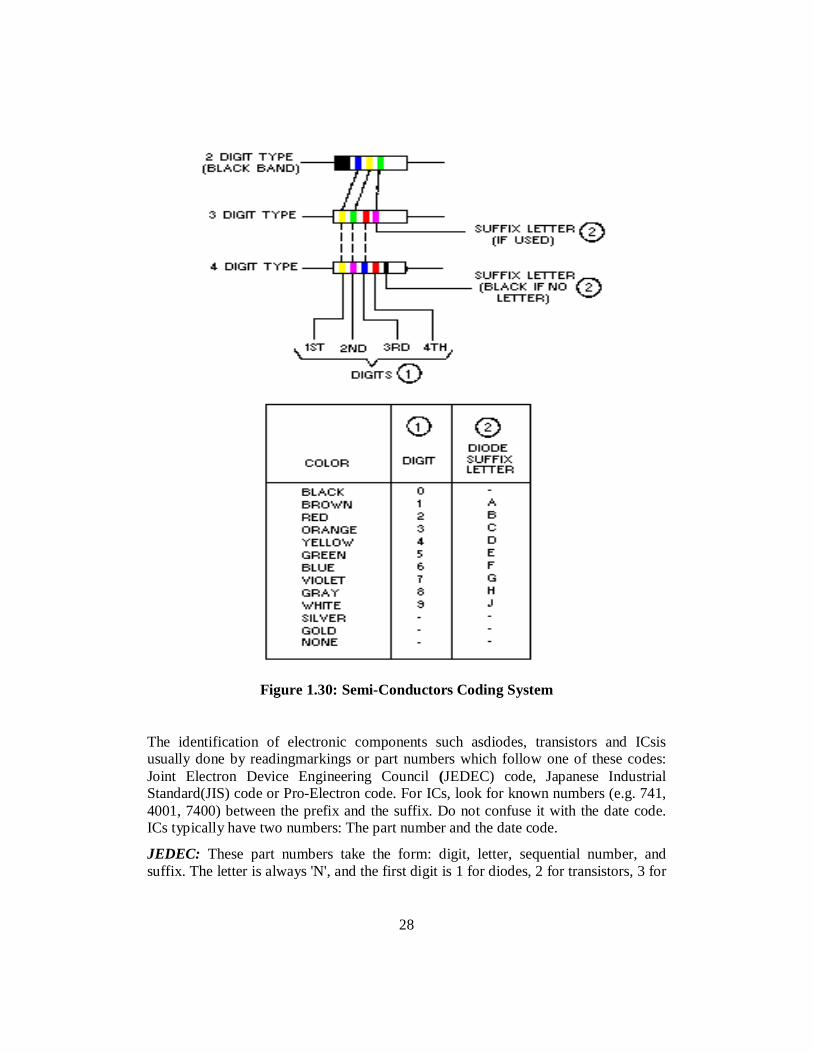
28
Figure 1.30: Semi-Conductors Coding System
The identification of electronic components such asdiodes, transistors and ICsis usually done by readingmarkings or part numbers which follow one of these codes: Joint Electron Device Engineering Council (JEDEC) code, Japanese Industrial Standard(JIS) code or Pro-Electron code. For ICs, look for known numbers (e.g. 741, 4001, 7400) between the prefix and the suffix. Do not confuse it with the date code. ICs typically have two numbers: The part number and the date code.
JEDEC: These part numbers take the form: digit, letter, sequential number, and suffix. The letter is always 'N', and the first digit is 1 for diodes, 2 for transistors, 3 for
29
four-leaded devices, and so forth as explained under diodes previously. But 4N and 5N are reserved for opto-couplers. The sequential numbers run from 100 to 9999 and indicate the approximate time the device was first made. If present, a suffix could indicate various things. For example, a 2N2222A is an enhanced version of a 2N2222. It has higher gain, frequency, and voltage ratings. Always check the data sheet. Examples: 1N914 (diode), 2N2222, 2N2222A, 2N904 (transistors).NOTE: When a metal-can version of a JEDEC transistor is remade in a plastic package, it is often given a number such as PN2222A which is a 2N2222A in a plastic case.
JIS: These part numbers take the form: digit, two letters, sequential number and optional suffix. Digits are 1 for diodes, 2 for transistors, and so forth. The letters indicate the type and intended application of the device according to the following code:
SA: PNP HF transistor; SB: PNP AF transistor; SC: NPNHF; SD: NPN AF transistor; SE: Diodes; SF: Thyristors; SG: Gunn devices; SH: UJT; SJ: P-channel FET; SK: N-channel FET; SM: Triac; SQ: LED; SR: Rectifier; SS: Signal diodes; ST: Avalanche diodes; SV: Varicaps; SZ: Zener diodes.
The sequential numbers run from 10-9999. The optional suffix indicates that the type is approved for use by various Japanese organizations. Since the code for transistors always begins with 2S, it is sometimes omitted; for example, a 2SC733 could be marked C733. Other examples include: 2SA1187, 2SB646, 2SC733.
Pro-Electron (European): These part numbers take the form: two letters, [letter], sequential number and suffix. The first letter indicates the material: A = Ge; B = Si; C = GaAs; R = compound materials. The second letter indicates the device type and intended application: A: diode, RF; B: diode, Varactor; C: transistor, AF, small signal;
30
D: transistor, AF, power; E: Tunnel diode; F: transistor, HF, small signal; K: Hall Effect device; L: Transistor, HF, power; N: Opto-coupler; P: Radiation sensitive device; Q: Radiation producing device; R: Thyristor, Low power; T: Thyristor, Power; U: Transistor, power, switching; Y: Rectifier; Z: Zener, or voltage regulator diode.
Moreover, the third letter indicates if the device is intended for industrial or commercial applications. It is usually a W, X, Y, or Z. The sequential numbers run from 100-9999. Examples include: BC108A, BAW68, BF239, and BFY51.Instead of 2N and so forth, some manufacturers use their own system of designations. Some common prefixes are: MJ: Motorola power, metal case; MJE: Motorola power, plastic case; MPS: Motorola low power, plastic case; MRF: Motorola HF, VHF and microwave transistor; RCA: RCA device; TIP: Texas Instruments (TI) power transistor, plastic case; TIPL: TI planar power transistor; TIS: TI small signal transistor (plastic case); ZT: Ferranti; ZTX: Ferranti. Examples: ZTX302, TIP31A, MJE3055.
Many manufacturers also make custom parts, or custom-label standard parts. Typi-cally, these include a mark or logo and part-number. When such parts hit the surplus market, they end up confusing people. As such, since data on these devices is not usually understandable, they are best used in such applications where the actual specifications are not critical. That notwithstanding, one of the important requirements of an electronic maintenance and repairman/woman is to be able to recognise electronic components, their part numbers and also interpret electronic circuit diagrams accurately. 1.5 Electronic Circuit Diagrams Diagrams are one of the main aids to maintenance, and it is therefore essential that they contain information which is relevant to the jobs for which they are provided, and that the information is presented in the best possible manner. For fault location, the most essential information is that concerning functional structure i.e. how the components are interconnected to perform their required function.In the past there have been a number of occasions on which circuit diagrams were criticized on the grounds of bad presentation and there have also been attempts to specify the requirements of a good diagram. Unfortunately, most of these efforts have resulted in little or no change in drawing practice. It is only recently that it has been shown how a wide range of complex electronic equipment diagrams can be greatly improved by the application of certain fundamental principles.
Bainbridge-Bell in 1953 put forward the idea that the main path in a circuit is made up of a number of links in a chain joining an input cause to an output effect. He suggested that the operation of a circuit is most easily followed if the chain is as straight as possible, since the reader's eye dislikes sudden changes in direction when scanning the diagram. Since we read from left to right, the cause to- effect path should go from left to right with any deviation clearly marked. Bainbridge-Bell also
31
suggested other changes, such as giving less emphasis to following the mechanical structure of the circuit being illustrated, and adopting more liberal use of sloping lines.
The British Standards Institution has also indicated where the emphasis should lie. BS530:1948 (Graphical symbols for telecommunications) states that diagrams should be drawn so that the main sequence of cause-to-effect goes from left to right, and/or from top to bottom. For instance, the input to Radio receive which is the aerial should always be on the left, and the output which is he speaker on the right. When this is impracticable, the direction of operation should be shown by an arrow. The linkages between components were once simple crossings of lines. With the arrival of computerized drafting, the connection of two intersecting wires was shown by a crossing of wires with a ‘dot’ or ‘blob’ to indicate a connection.
At the same time, the crossover was simplified to be the same crossing, but without a "dot". However, there was a danger of confusing the wires that were connected and not connected in this manner; if the dot was drawn too small or accidentally omitted (e.g. the "dot" could disappear after several passes through a photocopy machine). As such, the modern practice for representing a 4-way wire connection is to draw a straight wire and then to draw the other wires staggered along it with "dots" as connections, so as to form two separate T-junctions that brook no confusion and are clearly not a crossover. For crossing wires that are insulated from one another, a small semi-circle symbol is commonly used to show one wire "jumping over" the other wire (similar to how jumper wires are used).Balanced circuits are permitted exceptions from these recommendations. Components associated with each operational stage should be grouped together.
A more recent standard, BS3939:1966 (Graphical symbols for electrical power, telecommunications and electronics diagrams) does not contain guiding principles for drawing, but it does define a circuit diagram as: Ά diagram which depicts by means of symbols the components and their interconnections concerned in the operation of a circuit.
The aim should be to show the operation of the circuit as clearly as possible and therefore circuit diagrams do not necessarily depict spatial relationships of the various items and their connections. This indicates that emphasis should be on the clear illustration of function rather than mechanical structure.
Another professional body which has indicated a need for improved drawing standards is the Institution of Electronic and Radio Engineers. In a report of their Education and Training Committee published in 1964 it was stated that professional engineers do not pay sufficient attention to laying out a circuit diagram. The fundamental principle, which should be observed, but frequently is not, is that the layout should show the function of the various parts of the circuit and of the circuit overall. It is very useful when a circuit is laid out as a more detailed version of a block schematic. Clarity should not be sacrificed for the sake of neatness or appearance.
32
These examples give some indication of the characteristics of good diagrams, but unfortunately, good circuit diagrams are still rare.
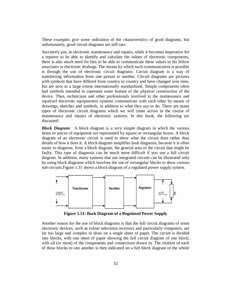
Succinctly put, in electronic maintenance and repairs, while it becomes imperative for a repairer to be able to identify and calculate the values of electronic components, there is also much need for him to be able to communicate these values to his fellow associates in electronic dealings. The means by which such communication is possible is through the use of electronic circuit diagrams. Circuit diagram is a way of transferring information from one person to another. Circuit diagrams are pictures with symbols that have differed from country to country and have changed over time, but are now to a large extent internationally standardized. Simple components often had symbols intended to represent some feature of the physical construction of the device. Thus, technicians and other professionals involved in the maintenance and repairsof electronic equipmentor systems communicate with each other by means of drawings, sketches and symbols, in addition to what they say or do. There are many types of electronic circuit diagrams which we will come across in the course of maintenance and repairs of electronic systems. In this book, the following are discussed:
Block Diagram: A block diagram is a very simple diagram in which the various items or pieces of equipment are represented by square or rectangular boxes. A block diagram of an electronic circuit is used to show what the circuit does rather than details of how it does it. A block diagram simplifies fault diagnosis, because it is often easier to diagnose, from a block diagram, the general area of the circuit that might be faulty. This type of diagnosis can be much more difficult if you use a full circuit diagram. In addition, many systems that use integrated circuits can be illustrated only by using block diagrams which involves the use of rectangular blocks to show various sub-circuits.Figure 1.31 shows a block diagram of a regulated power supply system.
Figure 1.31: Bock Diagram of a Regulated Power Supply
Another reason for the use of block diagrams is that the full circuit diagrams of some electronic devices, such as colour television receivers and particularly computers, are far too large and complex to draw on a single sheet of paper. The circuit is divided into blocks, with one sheet of paper showing the full circuit diagram of one block, with all (or most) of the components and connections drawn in. The relation of each of these blocks to one another is then indicated on a full block diagram of the whole
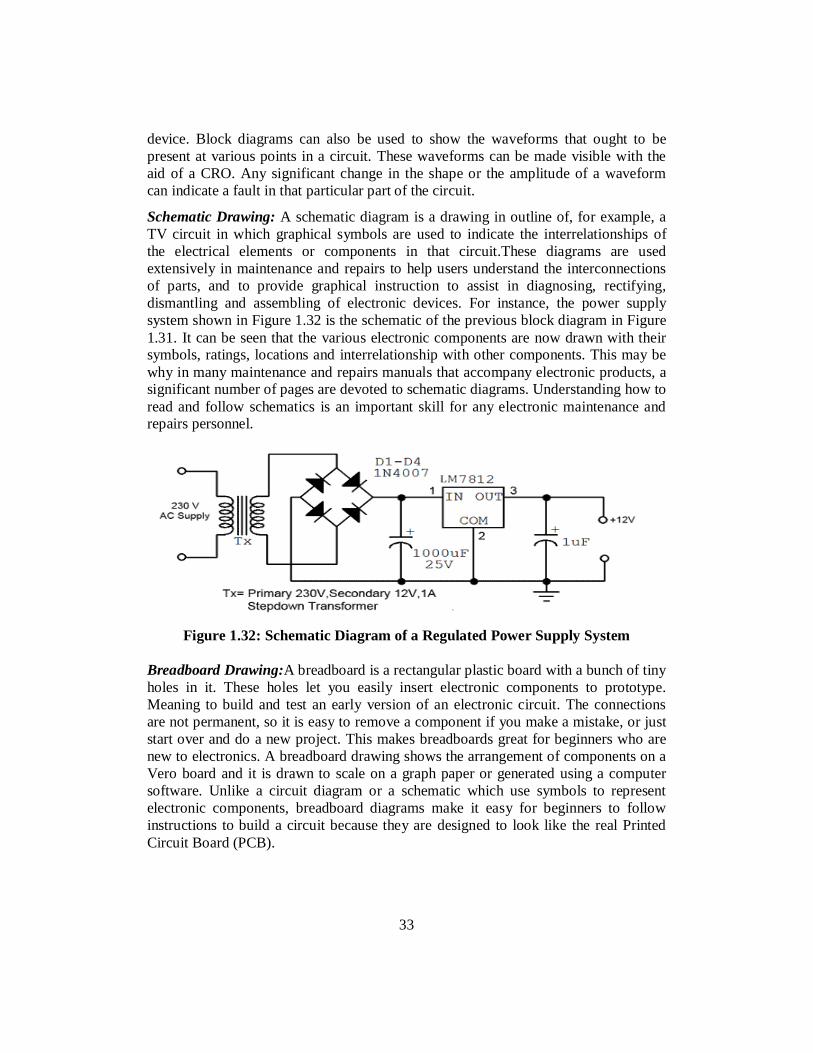
33
device. Block diagrams can also be used to show the waveforms that ought to be present at various points in a circuit. These waveforms can be made visible with the aid of a CRO. Any significant change in the shape or the amplitude of a waveform can indicate a fault in that particular part of the circuit.
Schematic Drawing: A schematic diagram is a drawing in outline of, for example, a TV circuit in which graphical symbols are used to indicate the interrelationships of the electrical elements or components in that circuit.These diagrams are used extensively in maintenance and repairs to help users understand the interconnections of parts, and to provide graphical instruction to assist in diagnosing, rectifying, dismantling and assembling of electronic devices. For instance, the power supply system shown in Figure 1.32 is the schematic of the previous block diagram in Figure 1.31. It can be seen that the various electronic components are now drawn with their symbols, ratings, locations and interrelationship with other components. This may be why in many maintenance and repairs manuals that accompany electronic products, a significant number of pages are devoted to schematic diagrams. Understanding how to read and follow schematics is an important skill for any electronic maintenance and repairs personnel.
Figure 1.32: Schematic Diagram of a Regulated Power Supply System
Breadboard Drawing:A breadboard is a rectangular plastic board with a bunch of tiny holes in it. These holes let you easily insert electronic components to prototype. Meaning to build and test an early version of an electronic circuit. The connections are not permanent, so it is easy to remove a component if you make a mistake, or just start over and do a new project. This makes breadboards great for beginners who are new to electronics. A breadboard drawing shows the arrangement of components on a Vero board and it is drawn to scale on a graph paper or generated using a computer software. Unlike a circuit diagram or a schematic which use symbols to represent electronic components, breadboard diagrams make it easy for beginners to follow instructions to build a circuit because they are designed to look like the real Printed Circuit Board (PCB).
34
Printed Circuit Board Layout Drawing: This is a drawing showing a sketch of the component layout and trace patterns for the PCB.A PCB is more real than a breadboard as it mechanically supports and electrically connects electronic components or electrical components using conductive tracks, pads and other features etched from one or more sheet layers of copper laminated onto and/or between sheet layers of a non-conductive substrate.
Printed Circuit Board Fabrication Drawing: This drawing shows how the Printed Circuit Board is to be fabricated.All board dimensions are indicated including those of holes.A fabrication drawing specifies how the PCB is to be manufactured. There are four major sections to a fabrication drawing which include: Board Illustration, Drill Chart, Section A-A, Notes, and Title Block. The board illustration shows the actual board outline with all cut-outs, corners and radii. Usually only the top side of the board is shown. All drilled holes are indicated with symbols linking them to the drill chart. Under a column labelled “Symbol,” the drill chart lists each drill symbol used in the board illustration. Other columns give further information regarding each hole type. The third section of the fabrication drawing is a view of the cross-section of the board, commonly referred to as a ‘sandwich.’ Items identified in this view are the overall board thickness, the layer numbers of the board, description of the layer (e.g., component side, VCC plane, etc.), dielectric thicknesses, and impedance information. If a Section A-A diagram is shown, as is usually the case, the board illustration must contain an indication of the point from where this view is seen.
Other types of electronic circuit diagramsinclude: Sheet Metal Drawing which is a two dimensional layout of the pattern required to produce a metal chassis or enclosure as well as packaging Drawing which shows how the final project appears from outside. It includes the location of LEDs, Switchesand Knobs etc.
1.6 Exercises 1. A surface-mounted resistor is numbered 234. What is the corresponding value
of its resistance? a. 230, 000Ω b. 234 000Ω c. 234Ω d. 234KΩ
2. Repair work entails: a. Fault detection b. Fault isolation c. Fault correction d. Fixing by replacing
3. Electronic maintenance is imperative so as to:
35
a. Avoid operational downtime b. Elongate equipment’s lifespan c. Restore equipment’s serviceable condition d. All of the above
4. Corrective maintenance is synonymous to: a. Condition-based maintenance b. Reliability-based maintenance c. Unscheduled maintenance d. Scheduled maintenance
5. ‘Esaki Diode’ is another name for: a. Zener Diode b. Tunnel Diode c. Schottky Diode d. Varactor Diode
6. A resistor has the following colour codes: Blue, Grey, Black, Red and Yellow. What is its corresponding rating: a. 68KΩ ±5% b. 64.7K Ω ± 10% c. 560K Ω ± 0.1% d. 67K Ω ±20%
7. Effective troubleshootingof a system requires the following except: a. System knowledge b. Procedural knowledge c. Strategic knowledge d. Structural knowledge
8. Reliability-based maintenance is: a. Expensive b. Carried out on any equipment c. More difficult than corrective maintenance d. Synonymous to condition-based maintenance
9. An active electronic component is the one in which: a. The flow of electronscan be controlled viaa terminal(s) b. Its state is determined by the applied voltage or current c. Electrical charges do not move d. Electrons move at a very fastrate
36
10. A capacitor with ‘104’ written on its body is said to have which of the following rating: a. 104 Pico Farad b. 1004 Pico Farad c. 100, 000 Pico Farad d. 1.4 × 10⁴ Pico Farad
11. With the aid ofa diagram(s) explain the following term(s): (a) Common Base Mode of amplification (b) Common CollectorMode of amplification (c) Common EmitterMode of amplification (d) Thyristor (e) Integrated Circuit (f) Pro-Electron (g) Electronic circuit diagram (h) JFET (i) MOSFET (j) SMOS (k) TTL (l) JIS (m) JEDEC.
12. How does a Tunnel Diode works?
13. What is the difference between LED and Varactor?
14. Explain how diodes can be used for half-wave and full-wave rectification. Support your answer with a diagram(s).
15. List and explain five types of capacitors and diodes each.
37
CHAPTER TWO 2.0 TEST EQUIPMENT, TOOLS AND MATERIALS IN
ELECTRONICMAINTENANCE AND REPAIRS For effective maintenance and repairs of electronic systems to be carried out, there is need tounderstand how to use the necessary test equipment, tools and materials such as Multimeter, Logic Probes, Frequency Counters; screwdriver, cutters, strippers; as well as ethanol, penetrating oil and so on.At the end of this chapter therefore, the readers should be able to explain: Test Equipmentin Electronic Maintenance and Repairs; Tools Needed inElectronic Maintenance and Repairs; and Materials Used in Electronic Maintenance and Repairs.
2.1 Test Equipment in Electronic Maintenance and Repairs Test equipment in electronic maintenance and repairs include voltmeters, oscilloscopes, logic probes, signal generators and various component testers that are used for the measurement, analysis, and diagnosis of electronic systems usually in the workshop. More so, the voltmeters, ammeters and ohmmeters may come as a unit in the form of Multimeters that can do the work of the individual instruments put together. Test equipmentare very vital in electronic troubleshooting as learnt in the later part of this book. In this section, let us look at what these equipment are meant for.
Multimeters:A multimeter is an electronic measuring instrument that combines several measurement functions in one unit. A typical multimeter can basically measure voltage, current, resistance among others. It is a hand-held device useful for basic maintenance and repairs of a wide array of domestic and industrial appliances. There are two types of multimeters which are Analogue Multimeter (AMM)and Digital Multimeter (DMM). Figure 2.1 shows some of the features of AMMs and DMMs. The difference between the twois majorly in the method of display of the measured variable. AMMs indicate values with the aid of a needle-like pointer while the DMMspresent measured values in form of digits or numbers. This gives the DMM an edge over the AMM type as the digital read-out makes reading easier and error free. More so, DMM is considered to be more accurate when it comes to measurement due to higher sensitivity compared to AMM. However, all these advantages come with higher cost as DMM is comparatively more expensive, hence, this book will cover lessons on how to use both multimeters since the analogue types are more affordable and popular among maintenance and repairmen/women.
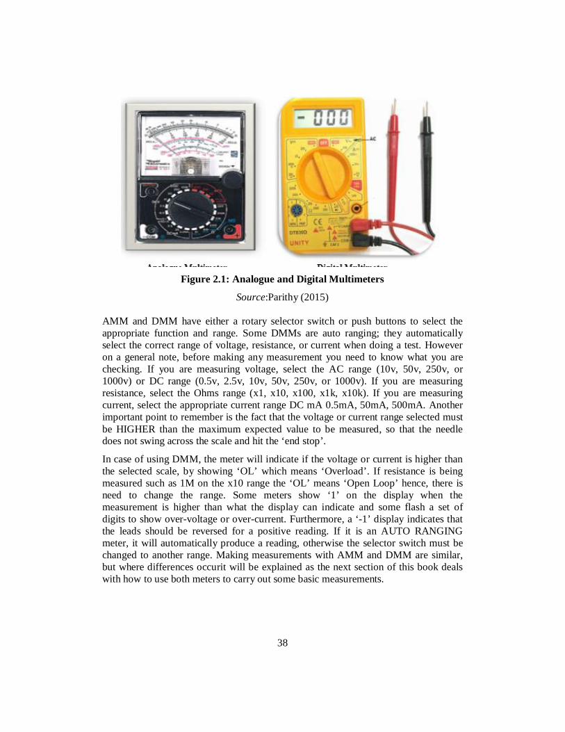
38
Figure 2.1: Analogue and Digital Multimeters
Source:Parithy (2015) AMM and DMM have either a rotary selector switch or push buttons to select the appropriate function and range. Some DMMs are auto ranging; they automatically select the correct range of voltage, resistance, or current when doing a test. However on a general note, before making any measurement you need to know what you are checking. If you are measuring voltage, select the AC range (10v, 50v, 250v, or 1000v) or DC range (0.5v, 2.5v, 10v, 50v, 250v, or 1000v). If you are measuring resistance, select the Ohms range (x1, x10, x100, x1k, x10k). If you are measuring current, select the appropriate current range DC mA 0.5mA, 50mA, 500mA. Another important point to remember is the fact that the voltage or current range selected must be HIGHER than the maximum expected value to be measured, so that the needle does not swing across the scale and hit the ‘end stop’.
In case of using DMM, the meter will indicate if the voltage or current is higher than the selected scale, by showing ‘OL’ which means ‘Overload’. If resistance is being measured such as 1M on the x10 range the ‘OL’ means ‘Open Loop’ hence, there is need to change the range. Some meters show ‘1’ on the display when the measurement is higher than what the display can indicate and some flash a set of digits to show over-voltage or over-current. Furthermore, a ‘-1’ display indicates that the leads should be reversed for a positive reading. If it is an AUTO RANGING meter, it will automatically produce a reading, otherwise the selector switch must be changed to another range. Making measurements with AMM and DMM are similar, but where differences occurit will be explained as the next section of this book deals with how to use both meters to carry out some basic measurements.
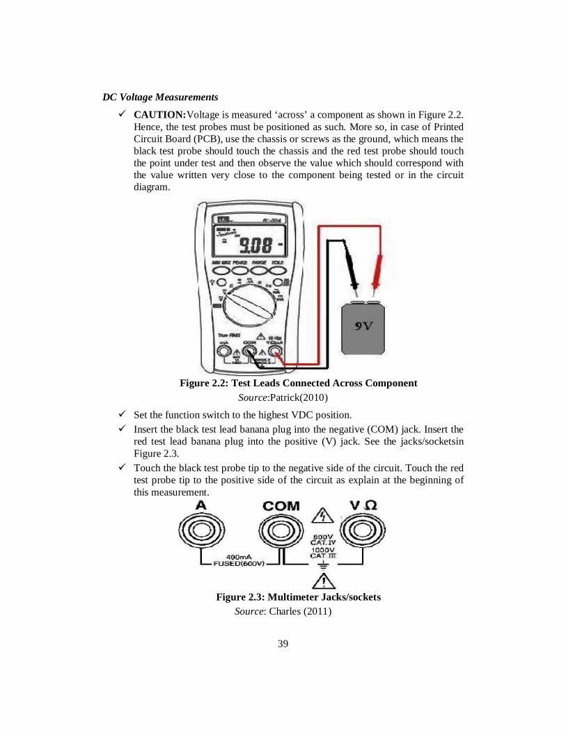
39
DC Voltage Measurements
CAUTION:Voltage is measured ‘across’ a component as shown in Figure 2.2. Hence, the test probes must be positioned as such. More so, in case of Printed Circuit Board (PCB), use the chassis or screws as the ground, which means the black test probe should touch the chassis and the red test probe should touch the point under test and then observe the value which should correspond with the value written very close to the component being tested or in the circuit diagram.
Figure 2.2: Test Leads Connected Across Component
Source:Patrick(2010)
Set the function switch to the highest VDC position. Insert the black test lead banana plug into the negative (COM) jack. Insert the
red test lead banana plug into the positive (V) jack. See the jacks/socketsin Figure 2.3.
Touch the black test probe tip to the negative side of the circuit. Touch the red test probe tip to the positive side of the circuit as explain at the beginning of this measurement.
Figure 2.3: Multimeter Jacks/sockets
Source: Charles (2011)
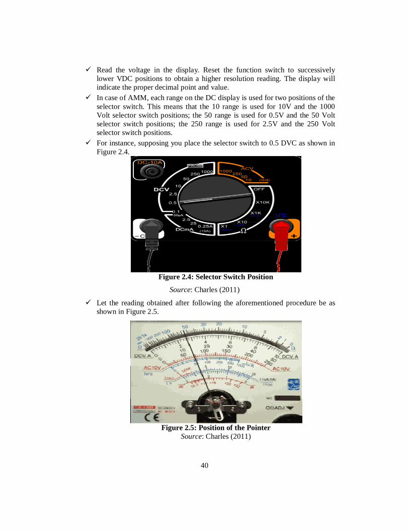
40
Read the voltage in the display. Reset the function switch to successively lower VDC positions to obtain a higher resolution reading. The display will indicate the proper decimal point and value.
In case of AMM, each range on the DC display is used for two positions of the selector switch. This means that the 10 range is used for 10V and the 1000 Volt selector switch positions; the 50 range is used for 0.5V and the 50 Volt selector switch positions; the 250 range is used for 2.5V and the 250 Volt selector switch positions.
For instance, supposing you place the selector switch to 0.5 DVC as shown in Figure 2.4.
Figure 2.4: Selector Switch Position
Source: Charles (2011)
Let the reading obtained after following the aforementioned procedure be as shown in Figure 2.5.
Figure 2.5: Position of the Pointer
Source: Charles (2011)
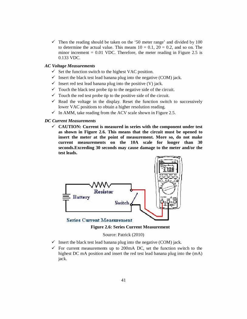
41
Then the reading should be taken on the ‘50 meter range’ and divided by 100 to determine the actual value. This means 10 = 0.1, 20 = 0.2, and so on. The minor increment = 0.01 VDC. Therefore, the meter reading in Figure 2.5 is 0.133 VDC.
AC Voltage Measurements Set the function switch to the highest VAC position. Insert the black test lead banana plug into the negative (COM) jack. Insert red test lead banana plug into the positive (V) jack. Touch the black test probe tip to the negative side of the circuit. Touch the red test probe tip to the positive side of the circuit. Read the voltage in the display. Reset the function switch to successively
lower VAC positions to obtain a higher resolution reading. In AMM, take reading from the ACV scale shown in Figure 2.5.
DC Current Measurements CAUTION: Current is measured in series with the component under test
as shown in Figure 2.6. This means that the circuit must be opened to insert the meter at the point of measurement. More so, do not make current measurements on the 10A scale for longer than 30 seconds.Exceeding 30 seconds may cause damage to the meter and/or the test leads.
Figure 2.6: Series Current Measurement
Source: Patrick (2010)
Insert the black test lead banana plug into the negative (COM) jack. For current measurements up to 200mA DC, set the function switch to the
highest DC mA position and insert the red test lead banana plug into the (mA) jack.
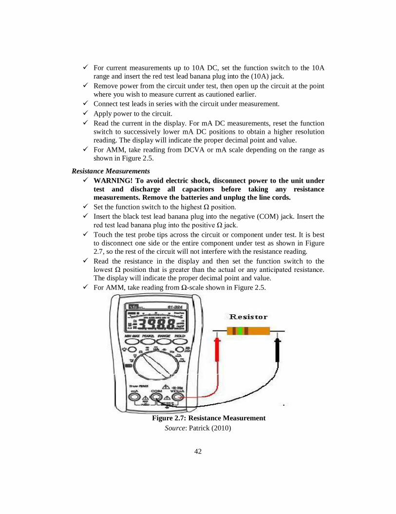
42
For current measurements up to 10A DC, set the function switch to the 10A range and insert the red test lead banana plug into the (10A) jack.
Remove power from the circuit under test, then open up the circuit at the point where you wish to measure current as cautioned earlier.
Connect test leads in series with the circuit under measurement. Apply power to the circuit. Read the current in the display. For mA DC measurements, reset the function
switch to successively lower mA DC positions to obtain a higher resolution reading. The display will indicate the proper decimal point and value.
For AMM, take reading from DCVA or mA scale depending on the range as shown in Figure 2.5.
Resistance Measurements WARNING! To avoid electric shock, disconnect power to the unit under
test and discharge all capacitors before taking any resistance measurements. Remove the batteries and unplug the line cords.
Set the function switch to the highest Ω position. Insert the black test lead banana plug into the negative (COM) jack. Insert the
red test lead banana plug into the positive Ω jack. Touch the test probe tips across the circuit or component under test. It is best
to disconnect one side or the entire component under test as shown in Figure 2.7, so the rest of the circuit will not interfere with the resistance reading.
Read the resistance in the display and then set the function switch to the lowest Ω position that is greater than the actual or any anticipated resistance. The display will indicate the proper decimal point and value.
For AMM, take reading from Ω-scale shown in Figure 2.5.
Figure 2.7: Resistance Measurement
Source: Patrick (2010)
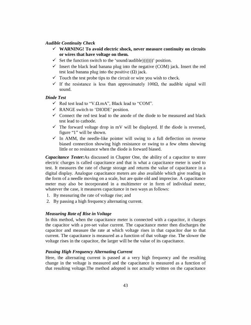
43
Audible Continuity Check WARNING! To avoid electric shock, never measure continuity on circuits
or wires that have voltage on them. Set the function switch to the ‘sound/audible)))))))’ position. Insert the black lead banana plug into the negative (COM) jack. Insert the red
test lead banana plug into the positive (Ω) jack. Touch the test probe tips to the circuit or wire you wish to check. If the resistance is less than approximately 100Ω, the audible signal will
sound.
Diode Test Red test lead to “V.Ω.mA”, Black lead to “COM”. RANGE switch to ‘DIODE’ position. Connect the red test lead to the anode of the diode to be measured and black
test lead to cathode. The forward voltage drop in mV will be displayed. If the diode is reversed,
figure “1” will be shown. In AMM, the needle-like pointer will swing to a full deflection on reverse
biased connection showing high resistance or swing to a few ohms showing little or no resistance when the diode is forward biased.
Capacitance Tester:As discussed in Chapter One, the ability of a capacitor to store electric charges is called capacitance and that is what a capacitance meter is used to test. It measures the rate of charge storage and returns the value of capacitance in a digital display. Analogue capacitance meters are also available which give reading in the form of a needle moving on a scale, but are quite old and imprecise. A capacitance meter may also be incorporated in a multimeter or in form of individual meter, whatever the case, it measures capacitance in two ways as follows: 1. By measuring the rate of voltage rise; and 2. By passing a high frequency alternating current. Measuring Rate of Rise in Voltage In this method, when the capacitance meter is connected with a capacitor, it charges the capacitor with a pre-set value current. The capacitance meter then discharges the capacitor and measure the rate at which voltage rises in that capacitor due to that current. The capacitance is measured as a function of that voltage rise. The slower the voltage rises in the capacitor, the larger will be the value of its capacitance. Passing High Frequency Alternating Current Here, the alternating current is passed at a very high frequency and the resulting change in the voltage is measured and the capacitance is measured as a function of that resulting voltage.The method adopted is not actually written on the capacitance
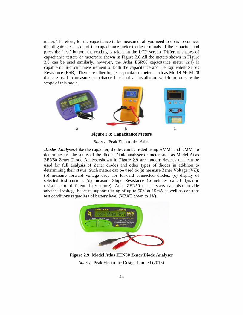
44
meter. Therefore, for the capacitance to be measured, all you need to do is to connect the alligator test leads of the capacitance meter to the terminals of the capacitor and press the ‘test’ button, the reading is taken on the LCD screen. Different shapes of capacitance testers or metersare shown in Figure 2.8.All the meters shown in Figure 2.8 can be used similarly, however, the Atlas ESR60 capacitance meter in(a) is capable of in-circuit measurement of both the capacitance and the Equivalent Series Resistance (ESR). There are other bigger capacitance meters such as Model MCM-20 that are used to measure capacitance in electrical installation which are outside the scope of this book.
Figure 2.8: Capacitance Meters
Source: Peak Electronics Atlas
Diodes Analyser:Like the capacitor, diodes can be tested using AMMs and DMMs to determine just the status of the diode. Diode analyser or meter such as Model Atlas ZEN50 Zener Diode Analysershown in Figure 2.9 are modern devices that can be used for full analysis of Zener diodes and other types of diodes in addition to determining their status. Such maters can be used to:(a) measure Zener Voltage (VZ); (b) measure forward voltage drop for forward connected diodes; (c) display of selected test current; (d) measure Slope Resistance (sometimes called dynamic resistance or differential resistance). Atlas ZEN50 or analysers can also provide advanced voltage boost to support testing of up to 50V at 15mA as well as constant test conditions regardless of battery level (VBAT down to 1V).
Figure 2.9: Model Atlas ZEN50 Zener Diode Analyser
Source: Peak Electronic Design Limited (2015)
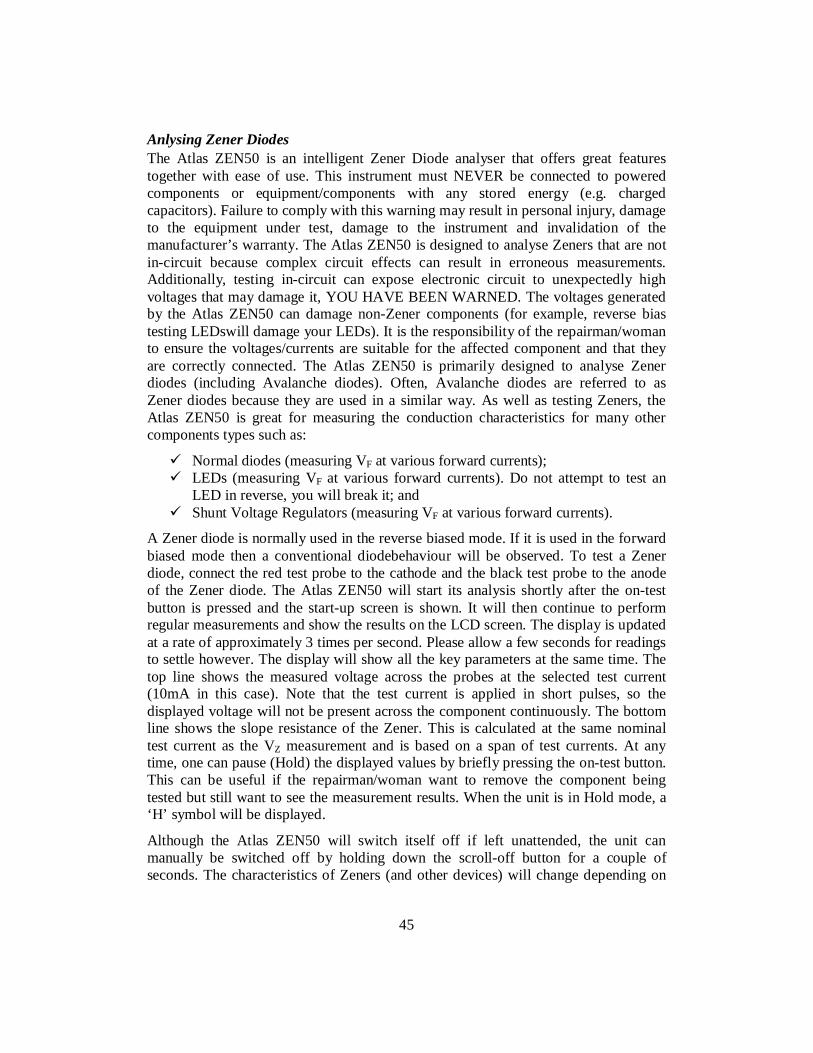
45
Anlysing Zener Diodes The Atlas ZEN50 is an intelligent Zener Diode analyser that offers great features together with ease of use. This instrument must NEVER be connected to powered components or equipment/components with any stored energy (e.g. charged capacitors). Failure to comply with this warning may result in personal injury, damage to the equipment under test, damage to the instrument and invalidation of the manufacturer’s warranty. The Atlas ZEN50 is designed to analyse Zeners that are not in-circuit because complex circuit effects can result in erroneous measurements. Additionally, testing in-circuit can expose electronic circuit to unexpectedly high voltages that may damage it, YOU HAVE BEEN WARNED. The voltages generated by the Atlas ZEN50 can damage non-Zener components (for example, reverse bias testing LEDswill damage your LEDs). It is the responsibility of the repairman/woman to ensure the voltages/currents are suitable for the affected component and that they are correctly connected. The Atlas ZEN50 is primarily designed to analyse Zener diodes (including Avalanche diodes). Often, Avalanche diodes are referred to as Zener diodes because they are used in a similar way. As well as testing Zeners, the Atlas ZEN50 is great for measuring the conduction characteristics for many other components types such as:
Normal diodes (measuring VF at various forward currents); LEDs (measuring VF at various forward currents). Do not attempt to test an
LED in reverse, you will break it; and Shunt Voltage Regulators (measuring VF at various forward currents).
A Zener diode is normally used in the reverse biased mode. If it is used in the forward biased mode then a conventional diodebehaviour will be observed. To test a Zener diode, connect the red test probe to the cathode and the black test probe to the anode of the Zener diode. The Atlas ZEN50 will start its analysis shortly after the on-test button is pressed and the start-up screen is shown. It will then continue to perform regular measurements and show the results on the LCD screen. The display is updated at a rate of approximately 3 times per second. Please allow a few seconds for readings to settle however. The display will show all the key parameters at the same time. The top line shows the measured voltage across the probes at the selected test current (10mA in this case). Note that the test current is applied in short pulses, so the displayed voltage will not be present across the component continuously. The bottom line shows the slope resistance of the Zener. This is calculated at the same nominal test current as the VZ measurement and is based on a span of test currents. At any time, one can pause (Hold) the displayed values by briefly pressing the on-test button. This can be useful if the repairman/woman want to remove the component being tested but still want to see the measurement results. When the unit is in Hold mode, a ‘H’ symbol will be displayed.
Although the Atlas ZEN50 will switch itself off if left unattended, the unit can manually be switched off by holding down the scroll-off button for a couple of seconds. The characteristics of Zeners (and other devices) will change depending on
46
the current flowing through the component. For Zeners in particular, it is common to see that the Zener voltage specified by the manufacturer is quoted at a certain test current. All Zeners will exhibit an increase in the Zener voltage as test current rises. More so, different test currents can be selected for different devices by briefly pressing the scroll-off button.
Analysing LED and Other Diodes The Atlas ZEN50 can measure the forward voltage drop of LEDs and other diodes as mentioned earlier. Take care to connect the LED or diode the right way round to ensure that it is not exposed to large reverse voltages. Do not attempt to test anLED in reverse with this instrument, even for a fraction of second, otherwise the LED will break up. The Anode (+) of the LED or diode should be connected to the red probe. The Cathode (-) of the LED or diode should be connected to the black probe. The unit will conveniently test almost any LED type, regardless of the LED’s forward voltage requirements. The current is controlled by the instrument and the voltage across the LED will automatically settle to the LED’s normal operating voltage (up to a maximum of 50V for long LED strings). It is important to appreciate that the test currents applied by the Atlas ZEN50 are very short and will result in very low apparent brightness of your LED. This does no harm but it does mean that your LED will appear much dimmer than you expect at the selected test current. For all the test currents, the voltage developed across the probes can rise to about 60V. This is to ensure that Zeners of up to 50V can be adequately tested. The test current is controlled to ensure that the same current flows regardless of the device under test (for the range of terminal voltages of 0V to 50V).
Although the current is electronically limited (to less than a peak of 35mA), it is important to be aware that 60V (across the open circuit probes) could potentially damage a sensitive component. For example, many LEDs can be damaged if the reverse voltage across them rises above 5V. There will be no problem when testing an LED in a forward direction (as the current is electronically limited and the voltage across the LED will automatically settle to the LED’s operating voltage). But if an LED is accidentally connected in reverse across the probes then the voltage could easily reach 60V and the LED would be damaged. In all cases, the voltage appearing across the probes will never be higher than 60V. Often the actual voltage will be limited by the device under test at the selected test current.
Transistor Tester:A transistortester/meter is an instrument for testingthe electrical behaviour of transistors and other solid state devices such as diodes. Like the diode meter, it comes in various shapes and models. A transistortester is used to find out whether an in-circuit transistor that has been working is still serviceable and can perform its previous functions effectively. The transistor’s ability to amplify electronic signals is checked using this type of tester. One of the advantages of this tester is that the transistor does not have to be removed from the circuit before the test can be performed.Transistor tester can be used to determine: (a) Forward-current gain or beta of transistor; (b) Base-Collector leakage current; and (c) Short-circuits from
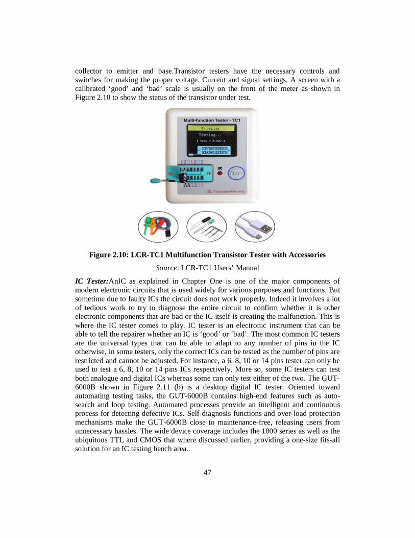
47
collector to emitter and base.Transistor testers have the necessary controls and switches for making the proper voltage. Current and signal settings. A screen with a calibrated ‘good’ and ‘bad’ scale is usually on the front of the meter as shown in Figure 2.10 to show the status of the transistor under test.
Figure 2.10: LCR-TC1 Multifunction Transistor Tester with Accessories
Source: LCR-TC1 Users’ Manual
IC Tester:AnIC as explained in Chapter One is one of the major components of modern electronic circuits that is used widely for various purposes and functions. But sometime due to faulty ICs the circuit does not work properly. Indeed it involves a lot of tedious work to try to diagnose the entire circuit to confirm whether it is other electronic components that are bad or the IC itself is creating the malfunction. This is where the IC tester comes to play. IC tester is an electronic instrument that can be able to tell the repairer whether an IC is ‘good’ or ‘bad’. The most common IC testers are the universal types that can be able to adapt to any number of pins in the IC otherwise, in some testers, only the correct ICs can be tested as the number of pins are restricted and cannot be adjusted. For instance, a 6, 8, 10 or 14 pins tester can only be used to test a 6, 8, 10 or 14 pins ICs respectively. More so, some IC testers can test both analogue and digital ICs whereas some can only test either of the two. The GUT-6000B shown in Figure 2.11 (b) is a desktop digital IC tester. Oriented toward automating testing tasks, the GUT-6000B contains high-end features such as auto-search and loop testing. Automated processes provide an intelligent and continuous process for detecting defective ICs. Self-diagnosis functions and over-load protection mechanisms make the GUT-6000B close to maintenance-free, releasing users from unnecessary hassles. The wide device coverage includes the 1800 series as well as the ubiquitous TTL and CMOS that where discussed earlier, providing a one-size fits-all solution for an IC testing bench area.
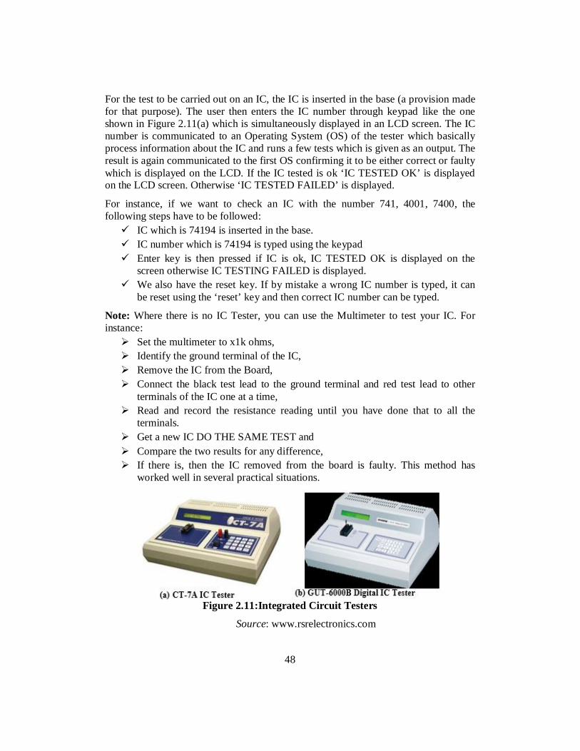
48
For the test to be carried out on an IC, the IC is inserted in the base (a provision made for that purpose). The user then enters the IC number through keypad like the one shown in Figure 2.11(a) which is simultaneously displayed in an LCD screen. The IC number is communicated to an Operating System (OS) of the tester which basically process information about the IC and runs a few tests which is given as an output. The result is again communicated to the first OS confirming it to be either correct or faulty which is displayed on the LCD. If the IC tested is ok ‘IC TESTED OK’ is displayed on the LCD screen. Otherwise ‘IC TESTED FAILED’ is displayed.
For instance, if we want to check an IC with the number 741, 4001, 7400, the following steps have to be followed: IC which is 74194 is inserted in the base. IC number which is 74194 is typed using the keypad Enter key is then pressed if IC is ok, IC TESTED OK is displayed on the
screen otherwise IC TESTING FAILED is displayed. We also have the reset key. If by mistake a wrong IC number is typed, it can
be reset using the ‘reset’ key and then correct IC number can be typed.
Note: Where there is no IC Tester, you can use the Multimeter to test your IC. For instance: Set the multimeter to x1k ohms, Identify the ground terminal of the IC, Remove the IC from the Board, Connect the black test lead to the ground terminal and red test lead to other
terminals of the IC one at a time, Read and record the resistance reading until you have done that to all the
terminals. Get a new IC DO THE SAME TEST and Compare the two results for any difference, If there is, then the IC removed from the board is faulty. This method has
worked well in several practical situations.
Figure 2.11:Integrated Circuit Testers
Source: www.rsrelectronics.com
49
Oscilloscopes:One of the most important electronic measuring instruments is the oscilloscope. Oscilloscopes have been in existence for a long time, since they were first devised in the 1930s. Initially, oscilloscopes were analogue but with the advent of digital technologies advanced oscilloscopes have since moved from being analogue to digital, and more features and measurement functionalities have been added, but some of the key basic considerations are still the same. Basically, the oscilloscope displays voltage versus time. More so, modern oscilloscopes can be used to display, add, subtract and manipulate two or more waveforms at a time. There are several waveforms that can be observed in oscilloscopes such as sine wave, damped sine waves, square and rectangular waves, saw-tooth and triangular waves, step waves, pulse and pulse train waves as well as complex waves.
Probing Basics Just like multimeter and other aforementioned maintenance and repair instruments, Oscilloscopes come with test probes. However, the probes in oscilloscopes are special requiring some level of expertise on how to handle them to carry out measurements with oscilloscopes. The method and techniques used in using these probes is what is referred to as probing in this book. Probing is one of the more overlooked areas but is equally as important as other aspects of oscilloscope. This is because as long as the signal going into the oscilloscope is being distorted by the probe, then it does not matter how good the oscilloscope or the person taking the measurement is since the measurement will end up yielding incorrect results. From a basic probe standpoint there are three factors to pay attention to. First is the physical attachment of the probe to the device under test. Second is to minimize the impact on the device under test. Third is to ensure adequate signal fidelity, making sure that what is seen on the oscilloscope is the most accurate representation of what is actually happening on the device under test.
Ideal Probe First let us consider an ideal probe. The ideal probe does not influence your device under test and would display the original signal on the oscilloscope without any distortion. For example, consider the setup in Figure 2.12. There are two ICs or chips and the measurement is probing the pulse in between them. The original signal is shown on the left. After attaching the ideal probe, what that receiver would see is exactly the original signal that was measured before the probe was attached. At the oscilloscope, ideally what is shown is exactly what is happening on the bus. Unfortunately, this type of ideal probe does not really exist and so in reality there will be some type of impact from the probe on the measurement which needs to be minimized.
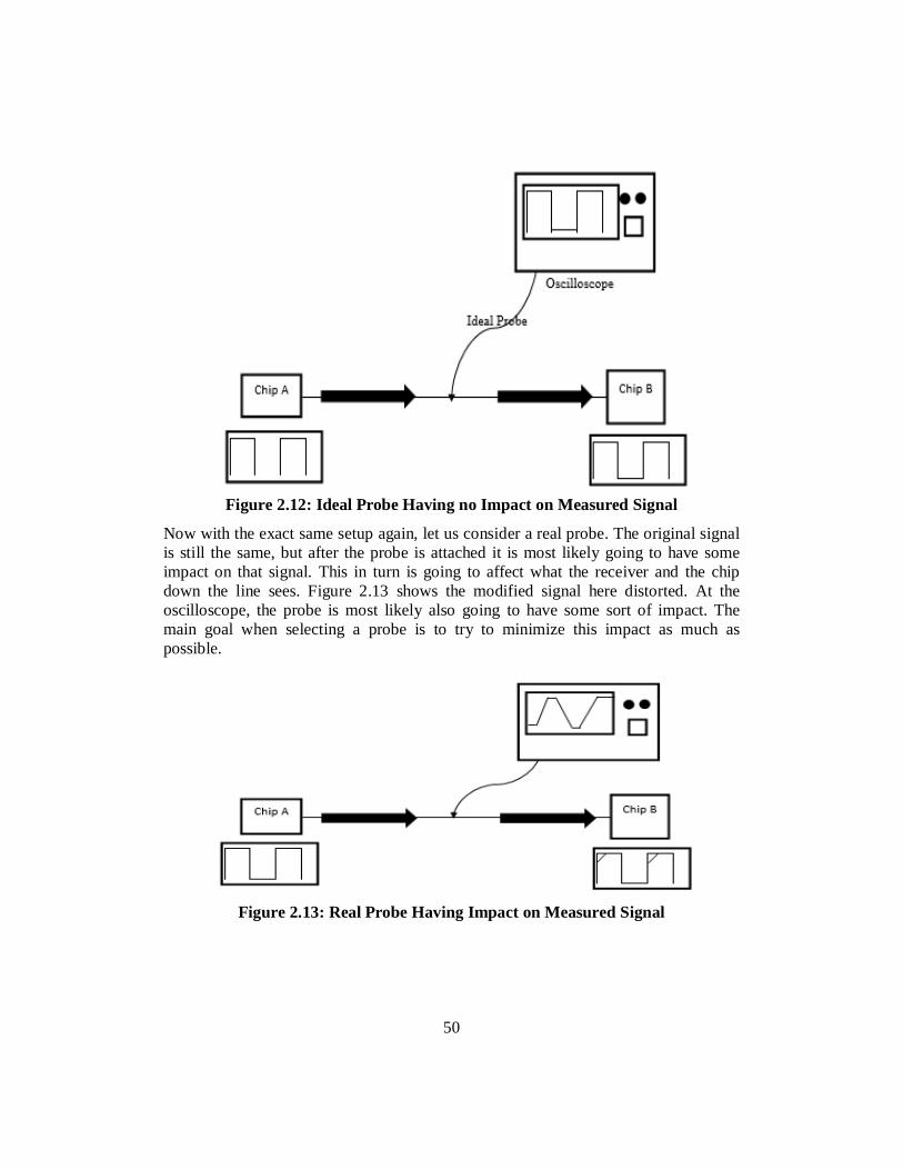
50
Figure 2.12: Ideal Probe Having no Impact on Measured Signal
Now with the exact same setup again, let us consider a real probe. The original signal is still the same, but after the probe is attached it is most likely going to have some impact on that signal. This in turn is going to affect what the receiver and the chip down the line sees. Figure 2.13 shows the modified signal here distorted. At the oscilloscope, the probe is most likely also going to have some sort of impact. The main goal when selecting a probe is to try to minimize this impact as much as possible.
Figure 2.13: Real Probe Having Impact on Measured Signal
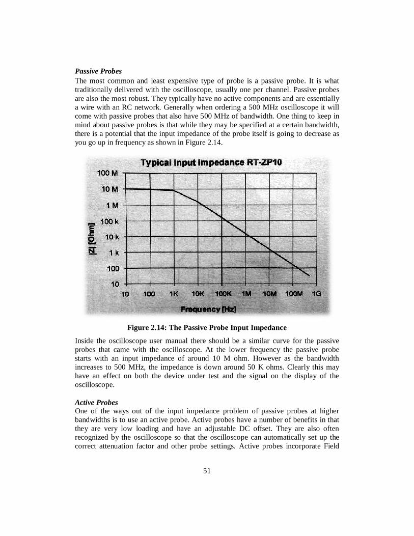
51
Passive Probes The most common and least expensive type of probe is a passive probe. It is what traditionally delivered with the oscilloscope, usually one per channel. Passive probes are also the most robust. They typically have no active components and are essentially a wire with an RC network. Generally when ordering a 500 MHz oscilloscope it will come with passive probes that also have 500 MHz of bandwidth. One thing to keep in mind about passive probes is that while they may be specified at a certain bandwidth, there is a potential that the input impedance of the probe itself is going to decrease as you go up in frequency as shown in Figure 2.14.
Figure 2.14: The Passive Probe Input Impedance
Inside the oscilloscope user manual there should be a similar curve for the passive probes that came with the oscilloscope. At the lower frequency the passive probe starts with an input impedance of around 10 M ohm. However as the bandwidth increases to 500 MHz, the impedance is down around 50 K ohms. Clearly this may have an effect on both the device under test and the signal on the display of the oscilloscope. Active Probes One of the ways out of the input impedance problem of passive probes at higher bandwidths is to use an active probe. Active probes have a number of benefits in that they are very low loading and have an adjustable DC offset. They are also often recognized by the oscilloscope so that the oscilloscope can automatically set up the correct attenuation factor and other probe settings. Active probes incorporate Field
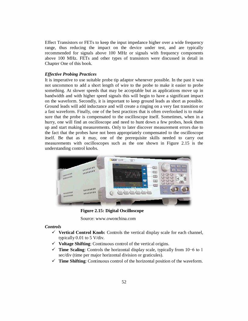
52
Effect Transistors or FETs to keep the input impedance higher over a wide frequency range, thus reducing the impact on the device under test, and are typically recommended for signals above 100 MHz or signals with frequency components above 100 MHz. FETs and other types of transistors were discussed in detail in Chapter One of this book. Effective Probing Practices It is imperative to use suitable probe tip adaptor whenever possible. In the past it was not uncommon to add a short length of wire to the probe to make it easier to probe something. At slower speeds that may be acceptable but as applications move up in bandwidth and with higher speed signals this will begin to have a significant impact on the waveform. Secondly, it is important to keep ground leads as short as possible. Ground leads will add inductance and will create a ringing on a very fast transition or a fast waveform. Finally, one of the best practices that is often overlooked is to make sure that the probe is compensated to the oscilloscope itself. Sometimes, when in a hurry, one will find an oscilloscope and need to hunt down a few probes, hook them up and start making measurements. Only to later discover measurement errors due to the fact that the probes have not been appropriately compensated to the oscilloscope itself. Be that as it may, one of the prerequisite skills needed to carry out measurements with oscilloscopes such as the one shown in Figure 2.15 is the understanding control knobs.
Figure 2.15: Digital Oscilloscope
Source: www.owonchina.com
Controls Vertical Control Knob: Controls the vertical display scale for each channel,
typically 0.01 to 5 V/div. Voltage Shifting: Continuous control of the vertical origins. Time Scaling: Controls the horizontal display scale, typically from 10−6 to 1
sec/div (time per major horizontal division or graticules). Time Shifting: Continuous control of the horizontal position of the waveform.
53
Trigger: Provides a way to control when t = 0, that is, what part of the waveform is at the left edge of the display.
This may be a threshold voltage level or slope. The oscilloscope will wait until the moment the threshold is crossed to begin the next display. This is important for stabilizing the display of periodic waveforms. Modern oscilloscopes perform many functions automatically, so the controls and display can be confusing. Along with measuring times and voltages accurately, oscilloscopes can also perform mathematical functions such as adding, subtracting, and multiplying waveforms. Identify the knobs on your oscilloscope. Connect a simple waveform from a function generator (amplitude ~1V, f ~100 Hz) into channel 1 and try to control its display. It should fill most of the display vertically; you should be able to show a fraction of a period or many periods at one time. If you cannot see it at all, you may need to refer to information for your specific instrument to turn on the display of voltage channel 1. Once you have learned the basic oscilloscope controls, here are a few other things that you should know about. On older analogue scopes, these are mostly controlled by a dedicated switch for each function. On digital scopes such as the one in Figure 2.15, there may be a pushbutton, but you may have to locate the options in a menu.
Coupling Mode(AC, DC, OR GROUND) Each channel will generally have three modes: DC Coupling: means that the signal is displayed without modification. AC Coupling: is used to eliminate the DC offset of a signal so it will be
centred around 0V. The oscilloscope applies a low-pass filter to the input. Ground: (or off) mode means that the 0-V level is displayed for that channel
(flat line). The voltage (vertical) shift knob can then be used to set the vertical origin.
Math Operations Most oscilloscopes can perform at least two mathematical operations on the waveforms: (a) Invert one or both channels (multiply by −1). (b) Add the channels together or (c) Subtract one from the other. The subtraction operation is often more important, since the ground lead of each channel has to be connected to a common circuit node. Then the voltage across a circuit element not connected to that point can be found from the difference between the two channels. The subtraction operation may be available as a combination of invert and add. Digital scopes may be capable of many other mathematical operations. Channel One versus Channel Two Mode Sometimes you do not need to see each waveform as it changes with time, but you want to know how two voltages change with respect to each other. In this mode, one channel is plotted horizontally and the other vertically, and the shape is traced as time evolves. This can be very helpful for finding the phase difference between two
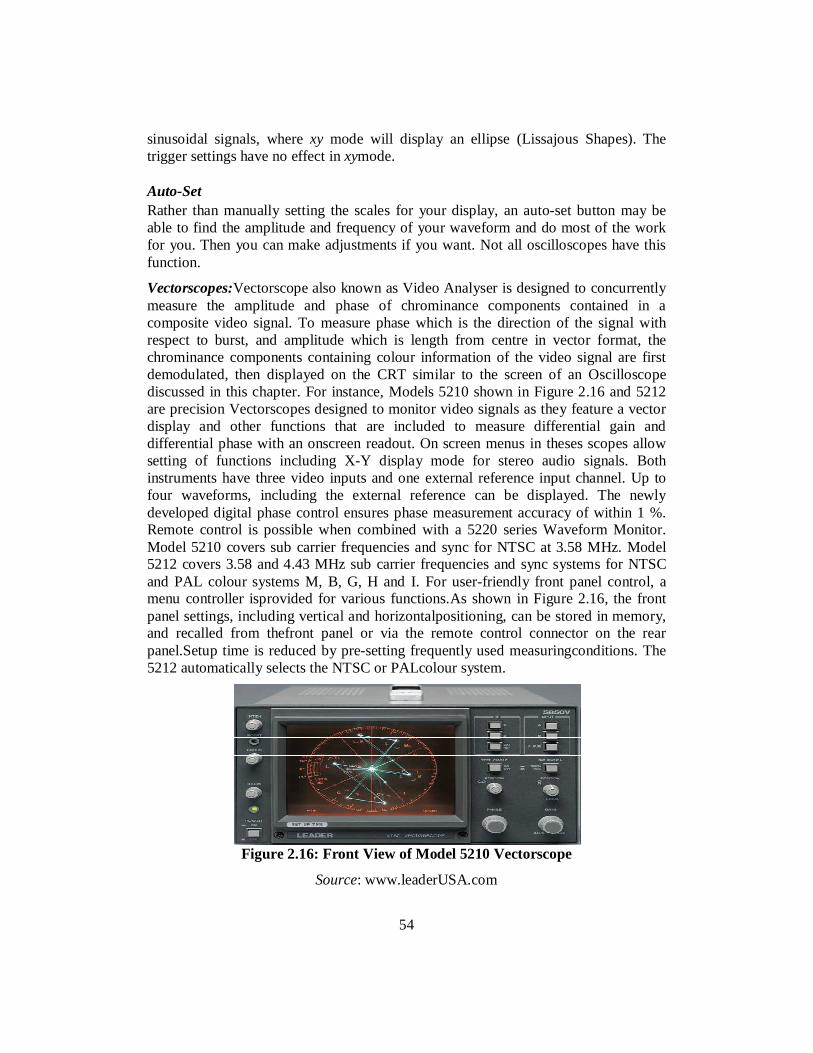
54
sinusoidal signals, where xy mode will display an ellipse (Lissajous Shapes). The trigger settings have no effect in xymode. Auto-Set Rather than manually setting the scales for your display, an auto-set button may be able to find the amplitude and frequency of your waveform and do most of the work for you. Then you can make adjustments if you want. Not all oscilloscopes have this function.
Vectorscopes:Vectorscope also known as Video Analyser is designed to concurrently measure the amplitude and phase of chrominance components contained in a composite video signal. To measure phase which is the direction of the signal with respect to burst, and amplitude which is length from centre in vector format, the chrominance components containing colour information of the video signal are first demodulated, then displayed on the CRT similar to the screen of an Oscilloscope discussed in this chapter. For instance, Models 5210 shown in Figure 2.16 and 5212 are precision Vectorscopes designed to monitor video signals as they feature a vector display and other functions that are included to measure differential gain and differential phase with an onscreen readout. On screen menus in theses scopes allow setting of functions including X-Y display mode for stereo audio signals. Both instruments have three video inputs and one external reference input channel. Up to four waveforms, including the external reference can be displayed. The newly developed digital phase control ensures phase measurement accuracy of within 1 %. Remote control is possible when combined with a 5220 series Waveform Monitor. Model 5210 covers sub carrier frequencies and sync for NTSC at 3.58 MHz. Model 5212 covers 3.58 and 4.43 MHz sub carrier frequencies and sync systems for NTSC and PAL colour systems M, B, G, H and I. For user-friendly front panel control, a menu controller isprovided for various functions.As shown in Figure 2.16, the front panel settings, including vertical and horizontalpositioning, can be stored in memory, and recalled from thefront panel or via the remote control connector on the rear panel.Setup time is reduced by pre-setting frequently used measuringconditions. The 5212 automatically selects the NTSC or PALcolour system.
Figure 2.16: Front View of Model 5210 Vectorscope
Source: www.leaderUSA.com
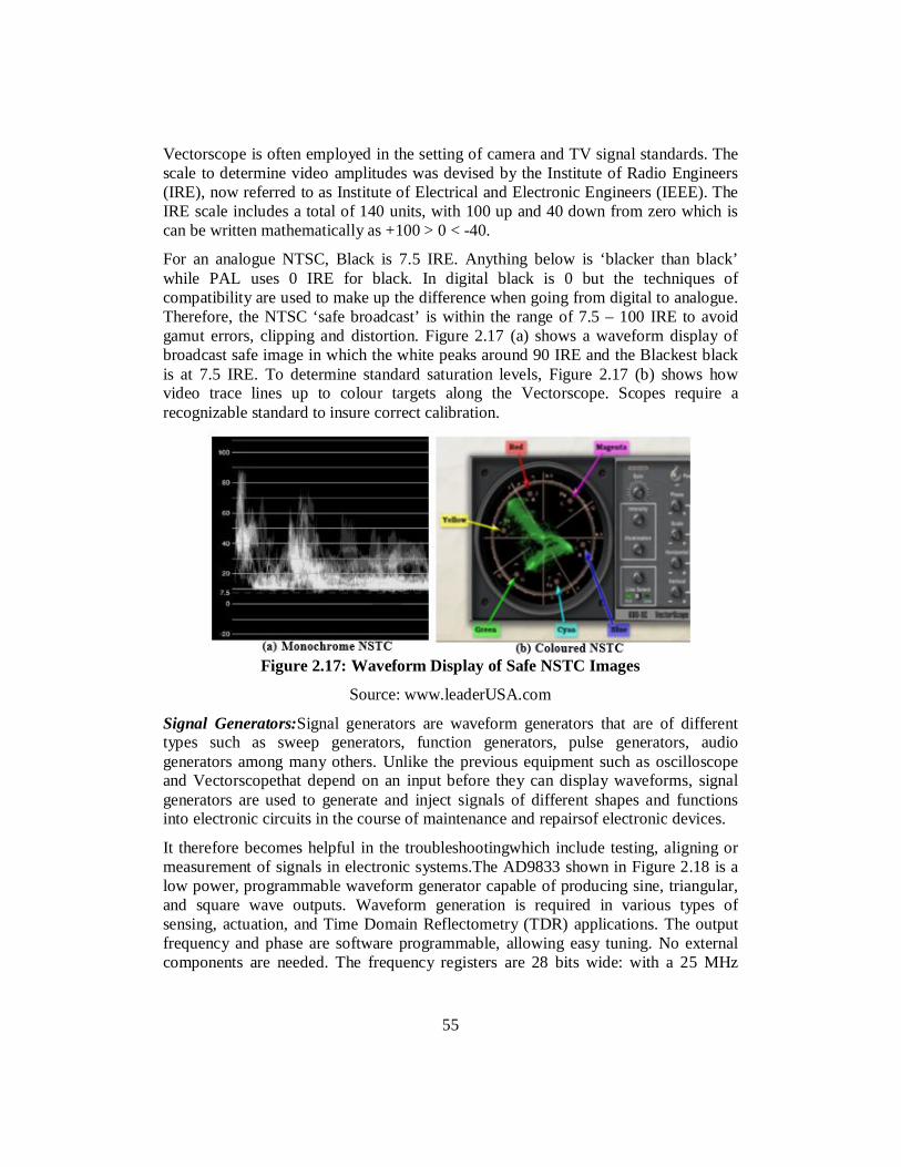
55
Vectorscope is often employed in the setting of camera and TV signal standards. The scale to determine video amplitudes was devised by the Institute of Radio Engineers (IRE), now referred to as Institute of Electrical and Electronic Engineers (IEEE). The IRE scale includes a total of 140 units, with 100 up and 40 down from zero which is can be written mathematically as +100 > 0 < -40.
For an analogue NTSC, Black is 7.5 IRE. Anything below is ‘blacker than black’ while PAL uses 0 IRE for black. In digital black is 0 but the techniques of compatibility are used to make up the difference when going from digital to analogue. Therefore, the NTSC ‘safe broadcast’ is within the range of 7.5 – 100 IRE to avoid gamut errors, clipping and distortion. Figure 2.17 (a) shows a waveform display of broadcast safe image in which the white peaks around 90 IRE and the Blackest black is at 7.5 IRE. To determine standard saturation levels, Figure 2.17 (b) shows how video trace lines up to colour targets along the Vectorscope. Scopes require a recognizable standard to insure correct calibration.
Figure 2.17: Waveform Display of Safe NSTC Images
Source: www.leaderUSA.com
Signal Generators:Signal generators are waveform generators that are of different types such as sweep generators, function generators, pulse generators, audio generators among many others. Unlike the previous equipment such as oscilloscope and Vectorscopethat depend on an input before they can display waveforms, signal generators are used to generate and inject signals of different shapes and functions into electronic circuits in the course of maintenance and repairsof electronic devices.
It therefore becomes helpful in the troubleshootingwhich include testing, aligning or measurement of signals in electronic systems.The AD9833 shown in Figure 2.18 is a low power, programmable waveform generator capable of producing sine, triangular, and square wave outputs. Waveform generation is required in various types of sensing, actuation, and Time Domain Reflectometry (TDR) applications. The output frequency and phase are software programmable, allowing easy tuning. No external components are needed. The frequency registers are 28 bits wide: with a 25 MHz
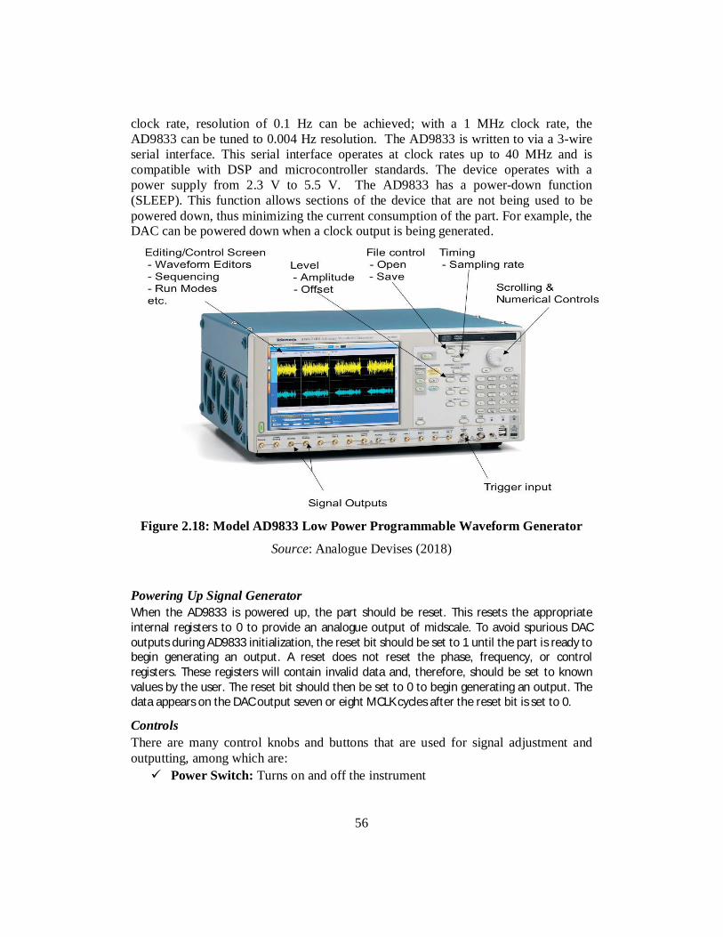
56
clock rate, resolution of 0.1 Hz can be achieved; with a 1 MHz clock rate, the AD9833 can be tuned to 0.004 Hz resolution. The AD9833 is written to via a 3-wire serial interface. This serial interface operates at clock rates up to 40 MHz and is compatible with DSP and microcontroller standards. The device operates with a power supply from 2.3 V to 5.5 V. The AD9833 has a power-down function (SLEEP). This function allows sections of the device that are not being used to be powered down, thus minimizing the current consumption of the part. For example, the DAC can be powered down when a clock output is being generated.
Figure 2.18: Model AD9833 Low Power Programmable Waveform Generator
Source: Analogue Devises (2018)
Powering Up Signal Generator When the AD9833 is powered up, the part should be reset. This resets the appropriate internal registers to 0 to provide an analogue output of midscale. To avoid spurious DAC outputs during AD9833 initialization, the reset bit should be set to 1 until the part is ready to begin generating an output. A reset does not reset the phase, frequency, or control registers. These registers will contain invalid data and, therefore, should be set to known values by the user. The reset bit should then be set to 0 to begin generating an output. The data appears on the DAC output seven or eight MCLK cycles after the reset bit is set to 0.
Controls There are many control knobs and buttons that are used for signal adjustment and outputting, among which are: Power Switch: Turns on and off the instrument
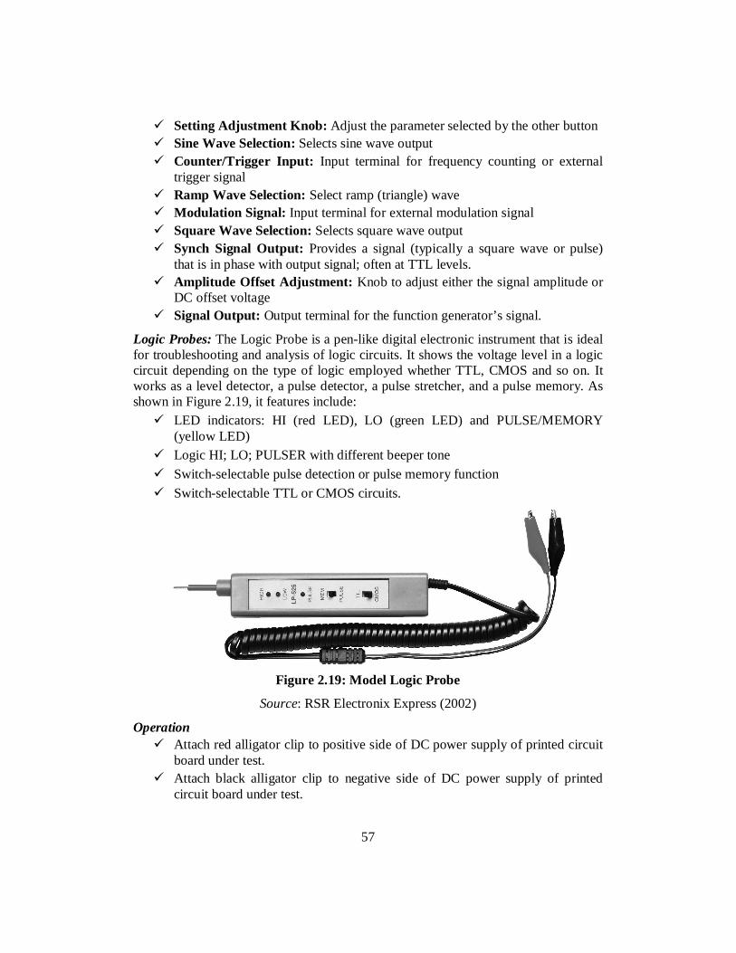
57
Setting Adjustment Knob: Adjust the parameter selected by the other button Sine Wave Selection: Selects sine wave output Counter/Trigger Input: Input terminal for frequency counting or external
trigger signal Ramp Wave Selection: Select ramp (triangle) wave Modulation Signal: Input terminal for external modulation signal Square Wave Selection: Selects square wave output Synch Signal Output: Provides a signal (typically a square wave or pulse)
that is in phase with output signal; often at TTL levels. Amplitude Offset Adjustment: Knob to adjust either the signal amplitude or
DC offset voltage Signal Output: Output terminal for the function generator’s signal.
Logic Probes: The Logic Probe is a pen-like digital electronic instrument that is ideal for troubleshooting and analysis of logic circuits. It shows the voltage level in a logic circuit depending on the type of logic employed whether TTL, CMOS and so on. It works as a level detector, a pulse detector, a pulse stretcher, and a pulse memory. As shown in Figure 2.19, it features include: LED indicators: HI (red LED), LO (green LED) and PULSE/MEMORY
(yellow LED) Logic HI; LO; PULSER with different beeper tone Switch-selectable pulse detection or pulse memory function Switch-selectable TTL or CMOS circuits.
Figure 2.19: Model Logic Probe
Source: RSR Electronix Express (2002)
Operation Attach red alligator clip to positive side of DC power supply of printed circuit
board under test. Attach black alligator clip to negative side of DC power supply of printed
circuit board under test.
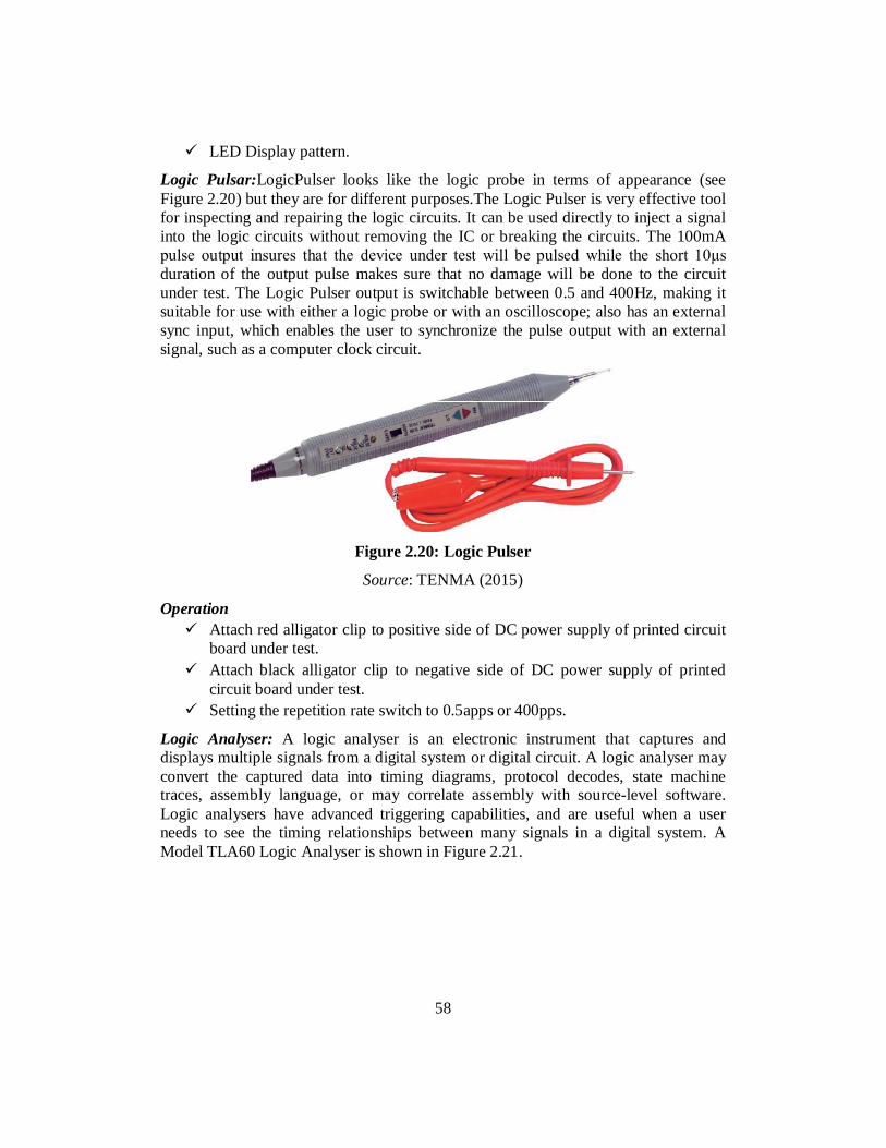
58
LED Display pattern.
Logic Pulsar:LogicPulser looks like the logic probe in terms of appearance (see Figure 2.20) but they are for different purposes.The Logic Pulser is very effective tool for inspecting and repairing the logic circuits. It can be used directly to inject a signal into the logic circuits without removing the IC or breaking the circuits. The 100mA pulse output insures that the device under test will be pulsed while the short 10μs duration of the output pulse makes sure that no damage will be done to the circuit under test. The Logic Pulser output is switchable between 0.5 and 400Hz, making it suitable for use with either a logic probe or with an oscilloscope; also has an external sync input, which enables the user to synchronize the pulse output with an external signal, such as a computer clock circuit.
Figure 2.20: Logic Pulser
Source: TENMA (2015)
Operation Attach red alligator clip to positive side of DC power supply of printed circuit
board under test. Attach black alligator clip to negative side of DC power supply of printed
circuit board under test. Setting the repetition rate switch to 0.5apps or 400pps.
Logic Analyser: A logic analyser is an electronic instrument that captures and displays multiple signals from a digital system or digital circuit. A logic analyser may convert the captured data into timing diagrams, protocol decodes, state machine traces, assembly language, or may correlate assembly with source-level software. Logic analysers have advanced triggering capabilities, and are useful when a user needs to see the timing relationships between many signals in a digital system. A Model TLA60 Logic Analyser is shown in Figure 2.21.
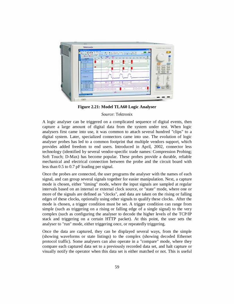
59
Figure 2.21: Model TLA60 Logic Analyser
Source: Tektronix
A logic analyser can be triggered on a complicated sequence of digital events, then capture a large amount of digital data from the system under test. When logic analysers first came into use, it was common to attach several hundred "clips" to a digital system. Later, specialized connectors came into use. The evolution of logic analyser probes has led to a common footprint that multiple vendors support, which provides added freedom to end users. Introduced in April, 2002, connector less technology (identified by several vendor-specific trade names: Compression Probing; Soft Touch; D-Max) has become popular. These probes provide a durable, reliable mechanical and electrical connection between the probe and the circuit board with less than 0.5 to 0.7 pF loading per signal.
Once the probes are connected, the user programs the analyser with the names of each signal, and can group several signals together for easier manipulation. Next, a capture mode is chosen, either "timing" mode, where the input signals are sampled at regular intervals based on an internal or external clock source, or "state" mode, where one or more of the signals are defined as "clocks", and data are taken on the rising or falling edges of these clocks, optionally using other signals to qualify these clocks. After the mode is chosen, a trigger condition must be set. A trigger condition can range from simple (such as triggering on a rising or falling edge of a single signal) to the very complex (such as configuring the analyser to decode the higher levels of the TCP/IP stack and triggering on a certain HTTP packet). At this point, the user sets the analyser to "run" mode, either triggering once, or repeatedly triggering.
Once the data are captured, they can be displayed several ways, from the simple (showing waveforms or state listings) to the complex (showing decoded Ethernet protocol traffic). Some analysers can also operate in a "compare" mode, where they compare each captured data set to a previously recorded data set, and halt capture or visually notify the operator when this data set is either matched or not. This is useful
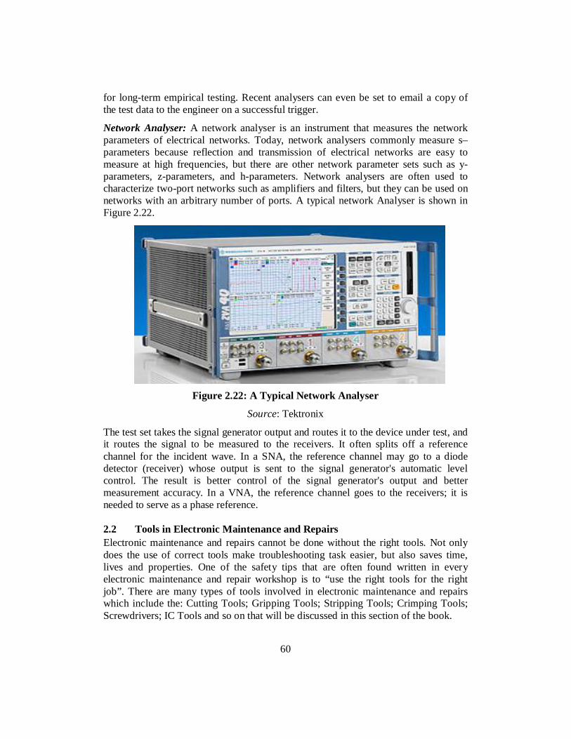
60
for long-term empirical testing. Recent analysers can even be set to email a copy of the test data to the engineer on a successful trigger.
Network Analyser: A network analyser is an instrument that measures the network parameters of electrical networks. Today, network analysers commonly measure s–parameters because reflection and transmission of electrical networks are easy to measure at high frequencies, but there are other network parameter sets such as y-parameters, z-parameters, and h-parameters. Network analysers are often used to characterize two-port networks such as amplifiers and filters, but they can be used on networks with an arbitrary number of ports. A typical network Analyser is shown in Figure 2.22.
Figure 2.22: A Typical Network Analyser
Source: Tektronix
The test set takes the signal generator output and routes it to the device under test, and it routes the signal to be measured to the receivers. It often splits off a reference channel for the incident wave. In a SNA, the reference channel may go to a diode detector (receiver) whose output is sent to the signal generator's automatic level control. The result is better control of the signal generator's output and better measurement accuracy. In a VNA, the reference channel goes to the receivers; it is needed to serve as a phase reference. 2.2 Tools in Electronic Maintenance and Repairs Electronic maintenance and repairs cannot be done without the right tools. Not only does the use of correct tools make troubleshooting task easier, but also saves time, lives and properties. One of the safety tips that are often found written in every electronic maintenance and repair workshop is to “use the right tools for the right job”. There are many types of tools involved in electronic maintenance and repairs which include the: Cutting Tools; Gripping Tools; Stripping Tools; Crimping Tools; Screwdrivers; IC Tools and so on that will be discussed in this section of the book.
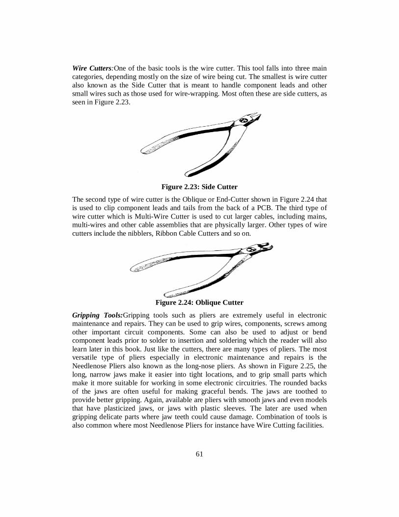
61
Wire Cutters:One of the basic tools is the wire cutter. This tool falls into three main categories, depending mostly on the size of wire being cut. The smallest is wire cutter also known as the Side Cutter that is meant to handle component leads and other small wires such as those used for wire-wrapping. Most often these are side cutters, as seen in Figure 2.23.
Figure 2.23: Side Cutter
The second type of wire cutter is the Oblique or End-Cutter shown in Figure 2.24 that is used to clip component leads and tails from the back of a PCB. The third type of wire cutter which is Multi-Wire Cutter is used to cut larger cables, including mains, multi-wires and other cable assemblies that are physically larger. Other types of wire cutters include the nibblers, Ribbon Cable Cutters and so on.
Figure 2.24: Oblique Cutter
Gripping Tools:Gripping tools such as pliers are extremely useful in electronic maintenance and repairs. They can be used to grip wires, components, screws among other important circuit components. Some can also be used to adjust or bend component leads prior to solder to insertion and soldering which the reader will also learn later in this book. Just like the cutters, there are many types of pliers. The most versatile type of pliers especially in electronic maintenance and repairs is the Needlenose Pliers also known as the long-nose pliers. As shown in Figure 2.25, the long, narrow jaws make it easier into tight locations, and to grip small parts which make it more suitable for working in some electronic circuitries. The rounded backs of the jaws are often useful for making graceful bends. The jaws are toothed to provide better gripping. Again, available are pliers with smooth jaws and even models that have plasticized jaws, or jaws with plastic sleeves. The later are used when gripping delicate parts where jaw teeth could cause damage. Combination of tools is also common where most Needlenose Pliers for instance have Wire Cutting facilities.
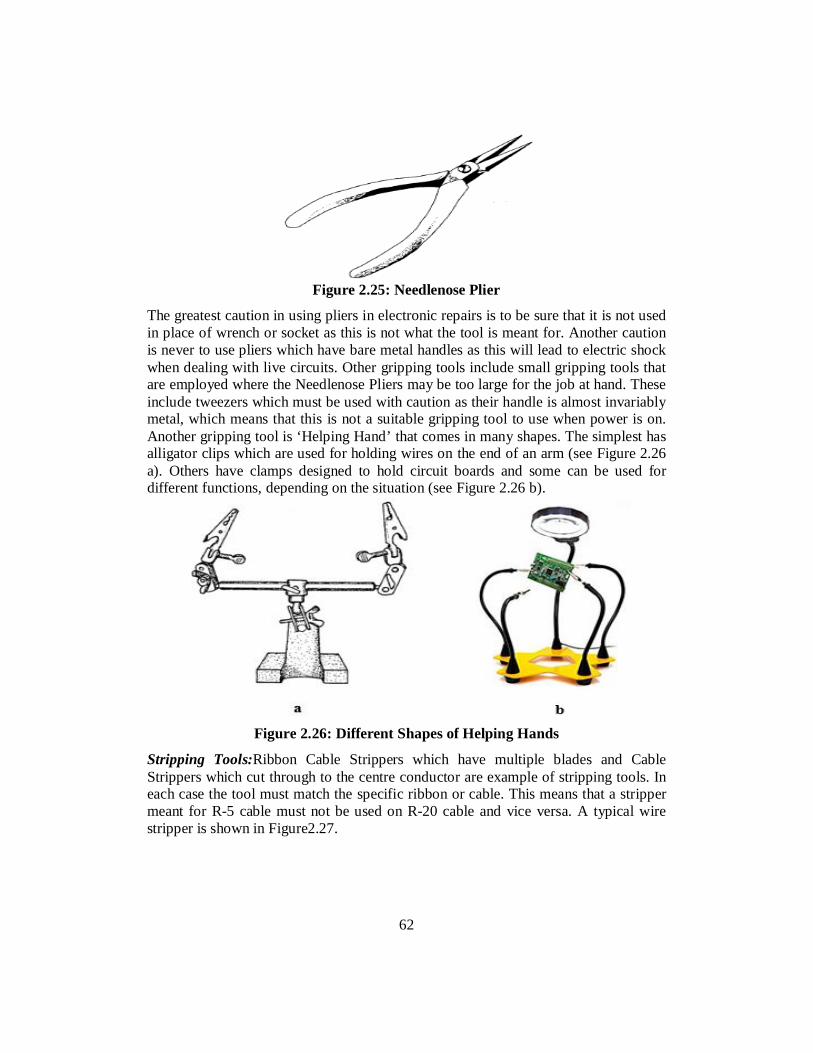
62
Figure 2.25: Needlenose Plier
The greatest caution in using pliers in electronic repairs is to be sure that it is not used in place of wrench or socket as this is not what the tool is meant for. Another caution is never to use pliers which have bare metal handles as this will lead to electric shock when dealing with live circuits. Other gripping tools include small gripping tools that are employed where the Needlenose Pliers may be too large for the job at hand. These include tweezers which must be used with caution as their handle is almost invariably metal, which means that this is not a suitable gripping tool to use when power is on. Another gripping tool is ‘Helping Hand’ that comes in many shapes. The simplest has alligator clips which are used for holding wires on the end of an arm (see Figure 2.26 a). Others have clamps designed to hold circuit boards and some can be used for different functions, depending on the situation (see Figure 2.26 b).
Figure 2.26: Different Shapes of Helping Hands
Stripping Tools:Ribbon Cable Strippers which have multiple blades and Cable Strippers which cut through to the centre conductor are example of stripping tools. In each case the tool must match the specific ribbon or cable. This means that a stripper meant for R-5 cable must not be used on R-20 cable and vice versa. A typical wire stripper is shown in Figure2.27.
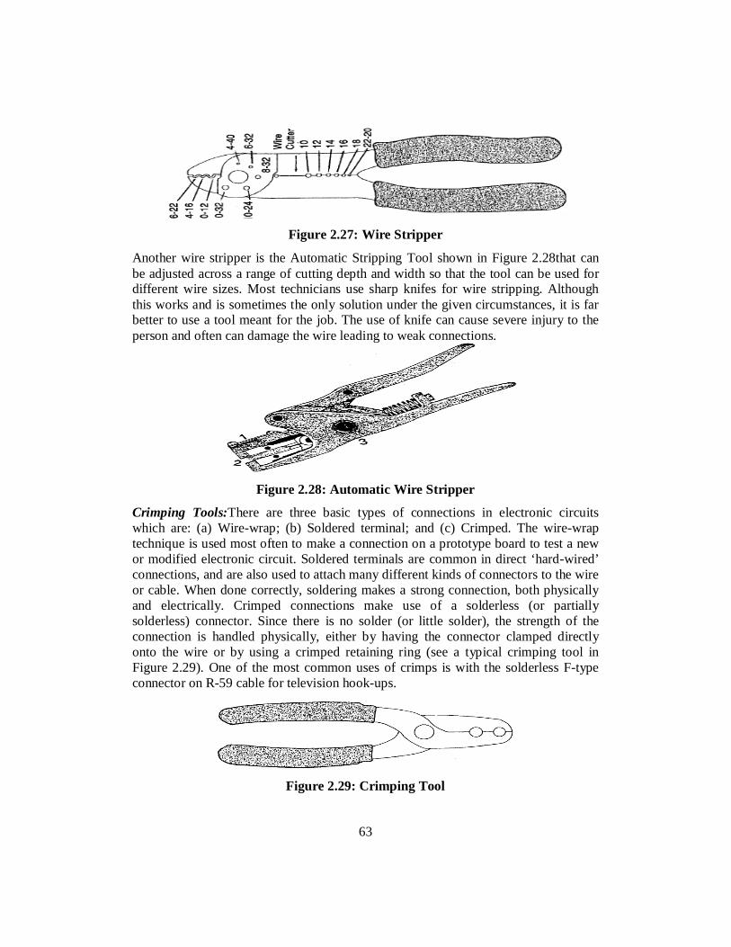
63
Figure 2.27: Wire Stripper
Another wire stripper is the Automatic Stripping Tool shown in Figure 2.28that can be adjusted across a range of cutting depth and width so that the tool can be used for different wire sizes. Most technicians use sharp knifes for wire stripping. Although this works and is sometimes the only solution under the given circumstances, it is far better to use a tool meant for the job. The use of knife can cause severe injury to the person and often can damage the wire leading to weak connections.
Figure 2.28: Automatic Wire Stripper
Crimping Tools:There are three basic types of connections in electronic circuits which are: (a) Wire-wrap; (b) Soldered terminal; and (c) Crimped. The wire-wrap technique is used most often to make a connection on a prototype board to test a new or modified electronic circuit. Soldered terminals are common in direct ‘hard-wired’ connections, and are also used to attach many different kinds of connectors to the wire or cable. When done correctly, soldering makes a strong connection, both physically and electrically. Crimped connections make use of a solderless (or partially solderless) connector. Since there is no solder (or little solder), the strength of the connection is handled physically, either by having the connector clamped directly onto the wire or by using a crimped retaining ring (see a typical crimping tool in Figure 2.29). One of the most common uses of crimps is with the solderless F-type connector on R-59 cable for television hook-ups.
Figure 2.29: Crimping Tool
64
It has been observed that some technicians make mistakes of using the wrong tool for the job. For instance, some will use pliers to crush the connector. Although this will often work, it will just as often make weak connection. Not only you are warned to use the right crimping tool, you must use it correctly. In general this means:
The insulation must be stripped away so that the conductor protrudes just slightly at the end, with the actual length being determined by the type of connector used;
The conductor is inserted into the connector or receptacle; The crimping tool is closed completely to make a secure crimp.
Screwdrivers and Nut Drivers:The range of screwdrivers and nut drivers manufactured today is impressive and sometimes confusing. Some devices will have standard screws and nuts, others will have metric and a few may even have a mixture of both. There are blade screw drivers and Philip head that come in different sizes such as small, medium and large. It is important that the head of the screw driver fits exactly into the head of the screw. If it does not, there is risk of damaging the screw, the screwdriver and possibly the user. As shown in Figure 2.30, there are also Jeweller’s Screwdrivers that can be purchased as a box set, containing 5, 6 or more screwdrivers with heads of different sizes. Often the set will include both the blade and Philips types.
Figure 2.30: Screwdrivers and Nut Drivers
Nut drivers are like wrench sockets mounted to screwdriver handles. Like regular sockets, the socket-ends of the nut driver come in a variety of sizes and may be either standard or metric.
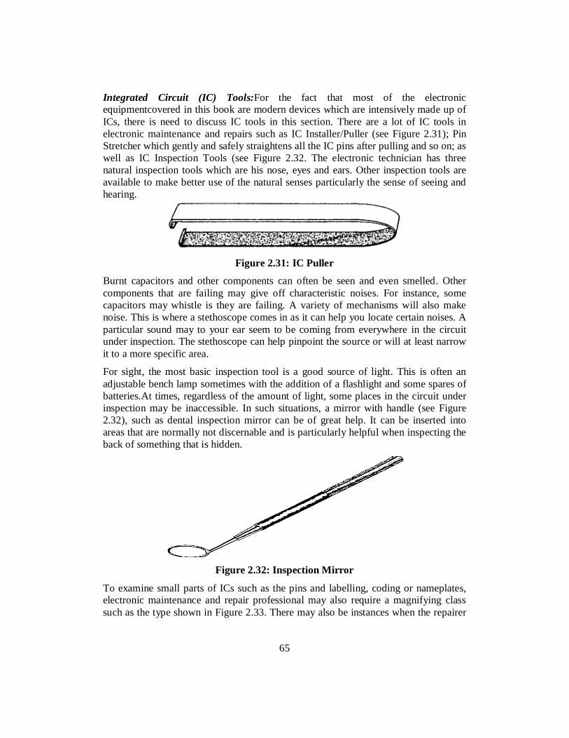
65
Integrated Circuit (IC) Tools:For the fact that most of the electronic equipmentcovered in this book are modern devices which are intensively made up of ICs, there is need to discuss IC tools in this section. There are a lot of IC tools in electronic maintenance and repairs such as IC Installer/Puller (see Figure 2.31); Pin Stretcher which gently and safely straightens all the IC pins after pulling and so on; as well as IC Inspection Tools (see Figure 2.32. The electronic technician has three natural inspection tools which are his nose, eyes and ears. Other inspection tools are available to make better use of the natural senses particularly the sense of seeing and hearing.
Figure 2.31: IC Puller
Burnt capacitors and other components can often be seen and even smelled. Other components that are failing may give off characteristic noises. For instance, some capacitors may whistle is they are failing. A variety of mechanisms will also make noise. This is where a stethoscope comes in as it can help you locate certain noises. A particular sound may to your ear seem to be coming from everywhere in the circuit under inspection. The stethoscope can help pinpoint the source or will at least narrow it to a more specific area.
For sight, the most basic inspection tool is a good source of light. This is often an adjustable bench lamp sometimes with the addition of a flashlight and some spares of batteries.At times, regardless of the amount of light, some places in the circuit under inspection may be inaccessible. In such situations, a mirror with handle (see Figure 2.32), such as dental inspection mirror can be of great help. It can be inserted into areas that are normally not discernable and is particularly helpful when inspecting the back of something that is hidden.
Figure 2.32: Inspection Mirror
To examine small parts of ICs such as the pins and labelling, coding or nameplates, electronic maintenance and repair professional may also require a magnifying class such as the type shown in Figure 2.33. There may also be instances when the repairer
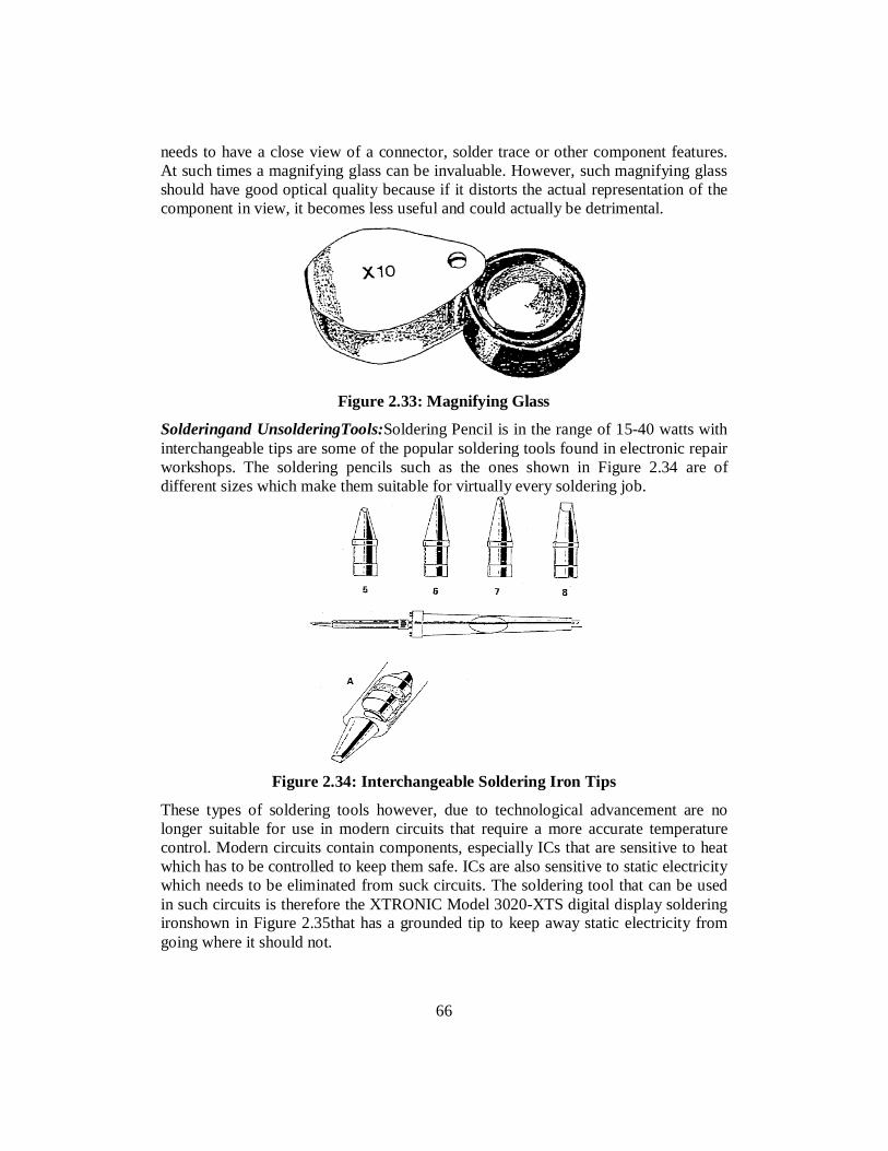
66
needs to have a close view of a connector, solder trace or other component features. At such times a magnifying glass can be invaluable. However, such magnifying glass should have good optical quality because if it distorts the actual representation of the component in view, it becomes less useful and could actually be detrimental.
Figure 2.33: Magnifying Glass
Solderingand UnsolderingTools:Soldering Pencil is in the range of 15-40 watts with interchangeable tips are some of the popular soldering tools found in electronic repair workshops. The soldering pencils such as the ones shown in Figure 2.34 are of different sizes which make them suitable for virtually every soldering job.
Figure 2.34: Interchangeable Soldering Iron Tips
These types of soldering tools however, due to technological advancement are no longer suitable for use in modern circuits that require a more accurate temperature control. Modern circuits contain components, especially ICs that are sensitive to heat which has to be controlled to keep them safe. ICs are also sensitive to static electricity which needs to be eliminated from suck circuits. The soldering tool that can be used in such circuits is therefore the XTRONIC Model 3020-XTS digital display soldering ironshown in Figure 2.35that has a grounded tip to keep away static electricity from going where it should not.
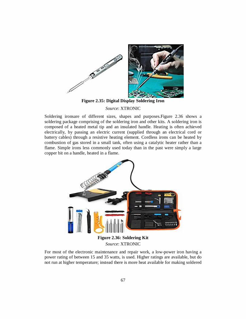
67
Figure 2.35: Digital Display Soldering Iron
Source: XTRONIC
Soldering ironsare of different sizes, shapes and purposes.Figure 2.36 shows a soldering package comprising of the soldering iron and other kits. A soldering iron is composed of a heated metal tip and an insulated handle. Heating is often achieved electrically, by passing an electric current (supplied through an electrical cord or battery cables) through a resistive heating element. Cordless irons can be heated by combustion of gas stored in a small tank, often using a catalytic heater rather than a flame. Simple irons less commonly used today than in the past were simply a large copper bit on a handle, heated in a flame.
Figure 2.36: Soldering Kit
Source: XTRONIC
For most of the electronic maintenance and repair work, a low-power iron having a power rating of between 15 and 35 watts, is used. Higher ratings are available, but do not run at higher temperature; instead there is more heat available for making soldered
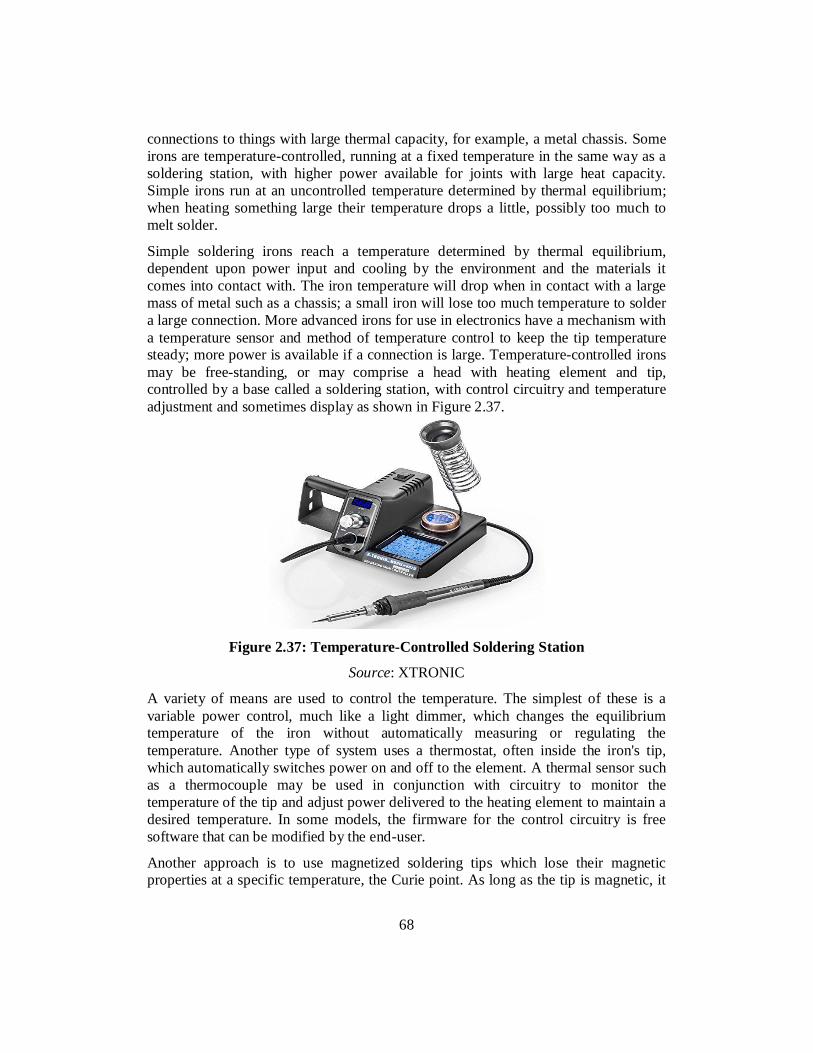
68
connections to things with large thermal capacity, for example, a metal chassis. Some irons are temperature-controlled, running at a fixed temperature in the same way as a soldering station, with higher power available for joints with large heat capacity. Simple irons run at an uncontrolled temperature determined by thermal equilibrium; when heating something large their temperature drops a little, possibly too much to melt solder.
Simple soldering irons reach a temperature determined by thermal equilibrium, dependent upon power input and cooling by the environment and the materials it comes into contact with. The iron temperature will drop when in contact with a large mass of metal such as a chassis; a small iron will lose too much temperature to solder a large connection. More advanced irons for use in electronics have a mechanism with a temperature sensor and method of temperature control to keep the tip temperature steady; more power is available if a connection is large. Temperature-controlled irons may be free-standing, or may comprise a head with heating element and tip, controlled by a base called a soldering station, with control circuitry and temperature adjustment and sometimes display as shown in Figure 2.37.
Figure 2.37: Temperature-Controlled Soldering Station
Source: XTRONIC
A variety of means are used to control the temperature. The simplest of these is a variable power control, much like a light dimmer, which changes the equilibrium temperature of the iron without automatically measuring or regulating the temperature. Another type of system uses a thermostat, often inside the iron's tip, which automatically switches power on and off to the element. A thermal sensor such as a thermocouple may be used in conjunction with circuitry to monitor the temperature of the tip and adjust power delivered to the heating element to maintain a desired temperature. In some models, the firmware for the control circuitry is free software that can be modified by the end-user.
Another approach is to use magnetized soldering tips which lose their magnetic properties at a specific temperature, the Curie point. As long as the tip is magnetic, it
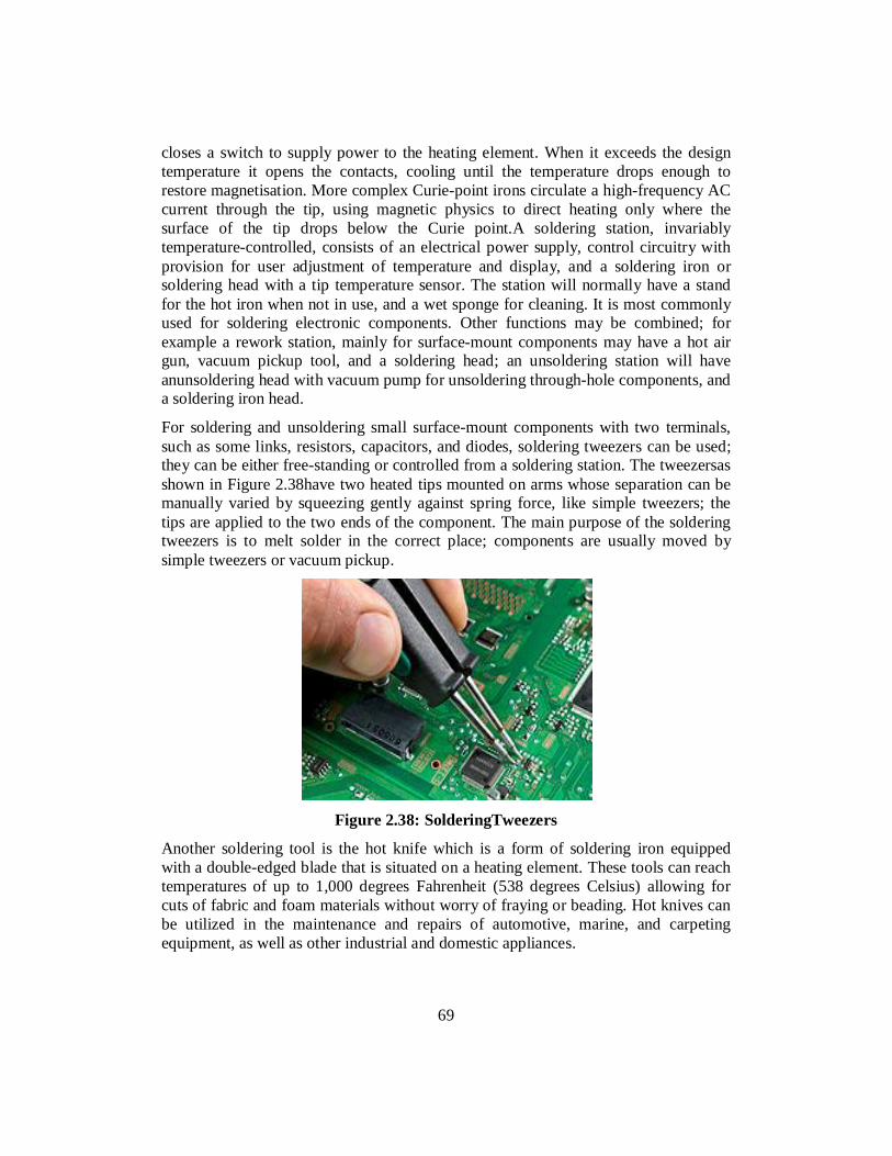
69
closes a switch to supply power to the heating element. When it exceeds the design temperature it opens the contacts, cooling until the temperature drops enough to restore magnetisation. More complex Curie-point irons circulate a high-frequency AC current through the tip, using magnetic physics to direct heating only where the surface of the tip drops below the Curie point.A soldering station, invariably temperature-controlled, consists of an electrical power supply, control circuitry with provision for user adjustment of temperature and display, and a soldering iron or soldering head with a tip temperature sensor. The station will normally have a stand for the hot iron when not in use, and a wet sponge for cleaning. It is most commonly used for soldering electronic components. Other functions may be combined; for example a rework station, mainly for surface-mount components may have a hot air gun, vacuum pickup tool, and a soldering head; an unsoldering station will have anunsoldering head with vacuum pump for unsoldering through-hole components, and a soldering iron head.
For soldering and unsoldering small surface-mount components with two terminals, such as some links, resistors, capacitors, and diodes, soldering tweezers can be used; they can be either free-standing or controlled from a soldering station. The tweezersas shown in Figure 2.38have two heated tips mounted on arms whose separation can be manually varied by squeezing gently against spring force, like simple tweezers; the tips are applied to the two ends of the component. The main purpose of the soldering tweezers is to melt solder in the correct place; components are usually moved by simple tweezers or vacuum pickup.
Figure 2.38: SolderingTweezers
Another soldering tool is the hot knife which is a form of soldering iron equipped with a double-edged blade that is situated on a heating element. These tools can reach temperatures of up to 1,000 degrees Fahrenheit (538 degrees Celsius) allowing for cuts of fabric and foam materials without worry of fraying or beading. Hot knives can be utilized in the maintenance and repairs of automotive, marine, and carpeting equipment, as well as other industrial and domestic appliances.
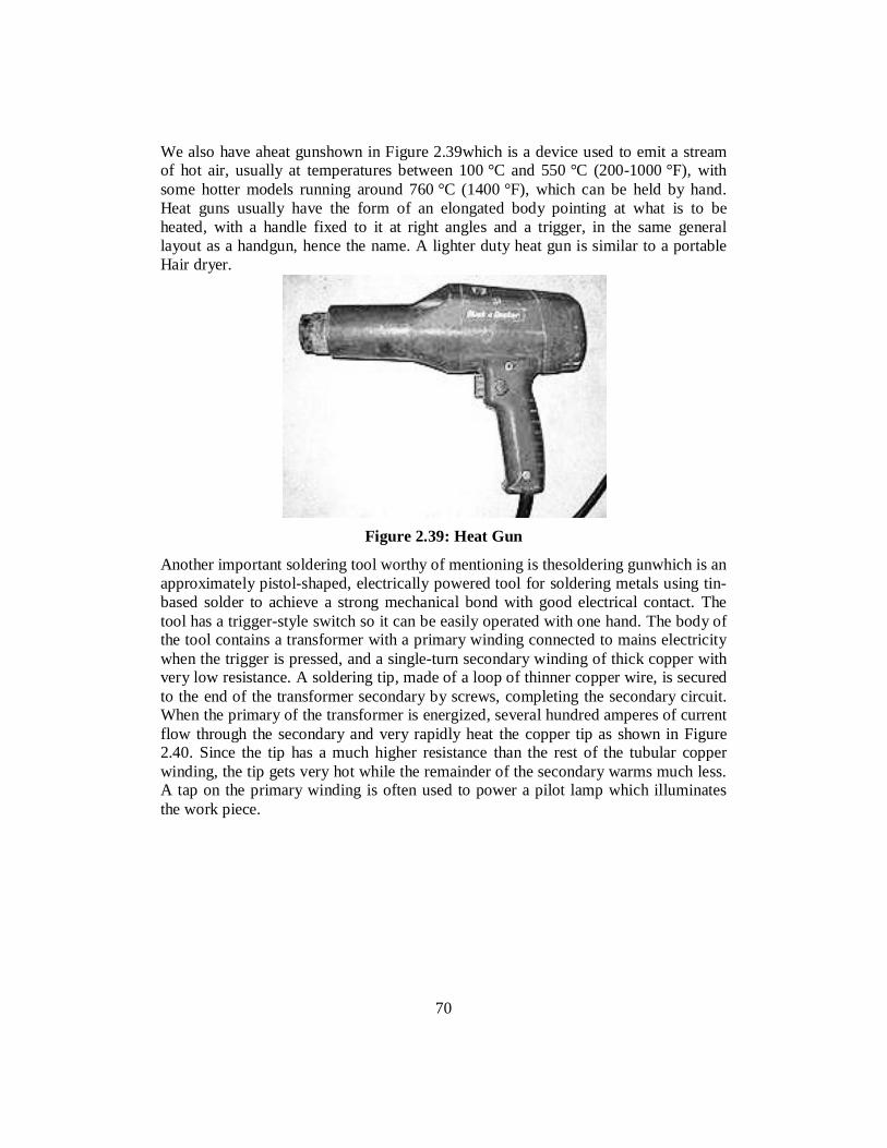
70
We also have aheat gunshown in Figure 2.39which is a device used to emit a stream of hot air, usually at temperatures between 100 °C and 550 °C (200-1000 °F), with some hotter models running around 760 °C (1400 °F), which can be held by hand. Heat guns usually have the form of an elongated body pointing at what is to be heated, with a handle fixed to it at right angles and a trigger, in the same general layout as a handgun, hence the name. A lighter duty heat gun is similar to a portable Hair dryer.
Figure 2.39: Heat Gun
Another important soldering tool worthy of mentioning is thesoldering gunwhich is an approximately pistol-shaped, electrically powered tool for soldering metals using tin-based solder to achieve a strong mechanical bond with good electrical contact. The tool has a trigger-style switch so it can be easily operated with one hand. The body of the tool contains a transformer with a primary winding connected to mains electricity when the trigger is pressed, and a single-turn secondary winding of thick copper with very low resistance. A soldering tip, made of a loop of thinner copper wire, is secured to the end of the transformer secondary by screws, completing the secondary circuit. When the primary of the transformer is energized, several hundred amperes of current flow through the secondary and very rapidly heat the copper tip as shown in Figure 2.40. Since the tip has a much higher resistance than the rest of the tubular copper winding, the tip gets very hot while the remainder of the secondary warms much less. A tap on the primary winding is often used to power a pilot lamp which illuminates the work piece.
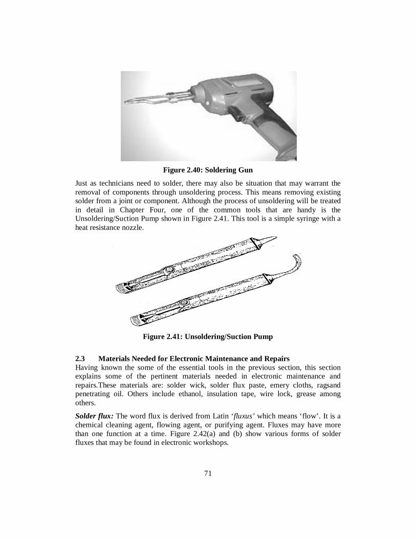
71
Figure 2.40: Soldering Gun
Just as technicians need to solder, there may also be situation that may warrant the removal of components through unsoldering process. This means removing existing solder from a joint or component. Although the process of unsoldering will be treated in detail in Chapter Four, one of the common tools that are handy is the Unsoldering/Suction Pump shown in Figure 2.41. This tool is a simple syringe with a heat resistance nozzle.
Figure 2.41: Unsoldering/Suction Pump
2.3 Materials Needed for Electronic Maintenance and Repairs Having known the some of the essential tools in the previous section, this section explains some of the pertinent materials needed in electronic maintenance and repairs.These materials are: solder wick, solder flux paste, emery cloths, ragsand penetrating oil. Others include ethanol, insulation tape, wire lock, grease among others.
Solder flux: The word flux is derived from Latin ‘fluxus’ which means ‘flow’. It is a chemical cleaning agent, flowing agent, or purifying agent. Fluxes may have more than one function at a time. Figure 2.42(a) and (b) show various forms of solder fluxes that may be found in electronic workshops.
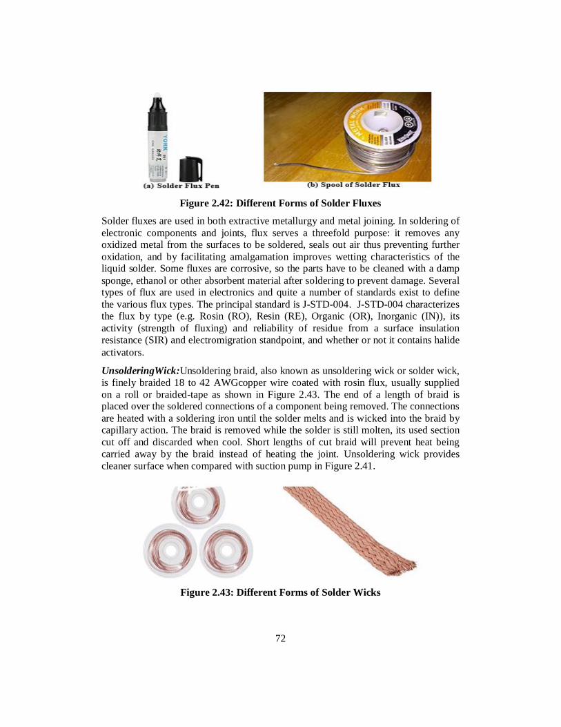
72
Figure 2.42: Different Forms of Solder Fluxes
Solder fluxes are used in both extractive metallurgy and metal joining. In soldering of electronic components and joints, flux serves a threefold purpose: it removes any oxidized metal from the surfaces to be soldered, seals out air thus preventing further oxidation, and by facilitating amalgamation improves wetting characteristics of the liquid solder. Some fluxes are corrosive, so the parts have to be cleaned with a damp sponge, ethanol or other absorbent material after soldering to prevent damage. Several types of flux are used in electronics and quite a number of standards exist to define the various flux types. The principal standard is J-STD-004. J-STD-004 characterizes the flux by type (e.g. Rosin (RO), Resin (RE), Organic (OR), Inorganic (IN)), its activity (strength of fluxing) and reliability of residue from a surface insulation resistance (SIR) and electromigration standpoint, and whether or not it contains halide activators.
UnsolderingWick:Unsoldering braid, also known as unsoldering wick or solder wick, is finely braided 18 to 42 AWGcopper wire coated with rosin flux, usually supplied on a roll or braided-tape as shown in Figure 2.43. The end of a length of braid is placed over the soldered connections of a component being removed. The connections are heated with a soldering iron until the solder melts and is wicked into the braid by capillary action. The braid is removed while the solder is still molten, its used section cut off and discarded when cool. Short lengths of cut braid will prevent heat being carried away by the braid instead of heating the joint. Unsoldering wick provides cleaner surface when compared with suction pump in Figure 2.41.
Figure 2.43: Different Forms of Solder Wicks
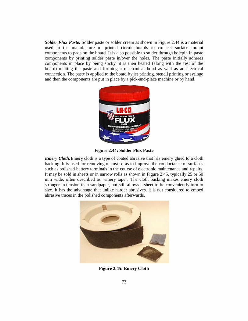
73
Solder Flux Paste: Solder paste or solder cream as shown in Figure 2.44 is a material used in the manufacture of printed circuit boards to connect surface mount components to pads on the board. It is also possible to solder through holepin in paste components by printing solder paste in/over the holes. The paste initially adheres components in place by being sticky, it is then heated (along with the rest of the board) melting the paste and forming a mechanical bond as well as an electrical connection. The paste is applied to the board by jet printing, stencil printing or syringe and then the components are put in place by a pick-and-place machine or by hand.
Figure 2.44: Solder Flux Paste
Emery Cloth:Emery cloth is a type of coated abrasive that has emery glued to a cloth backing. It is used for removing of rust so as to improve the conductance of surfaces such as polished battery terminals in the course of electronic maintenance and repairs. It may be sold in sheets or in narrow rolls as shown in Figure 2.45, typically 25 or 50 mm wide, often described as "emery tape". The cloth backing makes emery cloth stronger in tension than sandpaper, but still allows a sheet to be conveniently torn to size. It has the advantage that unlike harder abrasives, it is not considered to embed abrasive traces in the polished components afterwards.
Figure 2.45: Emery Cloth
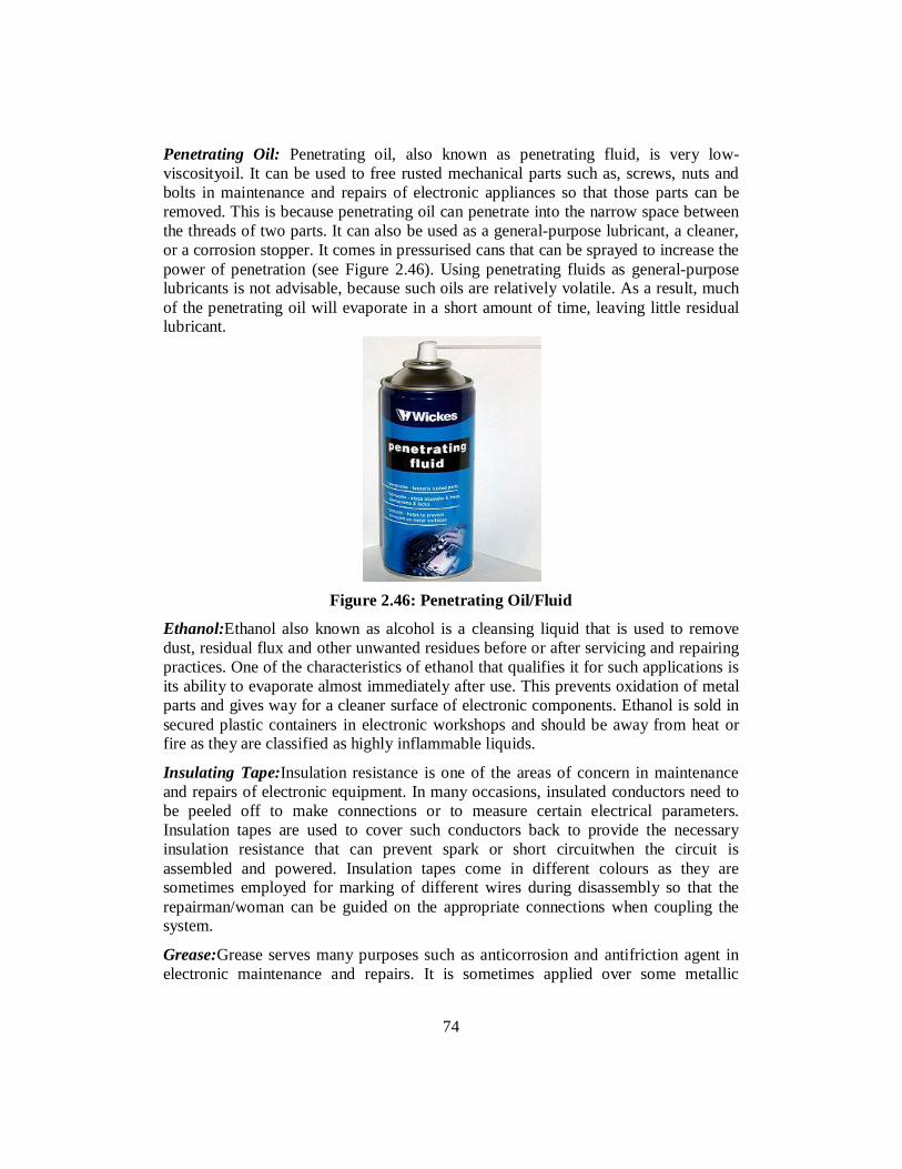
74
Penetrating Oil: Penetrating oil, also known as penetrating fluid, is very low-viscosityoil. It can be used to free rusted mechanical parts such as, screws, nuts and bolts in maintenance and repairs of electronic appliances so that those parts can be removed. This is because penetrating oil can penetrate into the narrow space between the threads of two parts. It can also be used as a general-purpose lubricant, a cleaner, or a corrosion stopper. It comes in pressurised cans that can be sprayed to increase the power of penetration (see Figure 2.46). Using penetrating fluids as general-purpose lubricants is not advisable, because such oils are relatively volatile. As a result, much of the penetrating oil will evaporate in a short amount of time, leaving little residual lubricant.
Figure 2.46: Penetrating Oil/Fluid
Ethanol:Ethanol also known as alcohol is a cleansing liquid that is used to remove dust, residual flux and other unwanted residues before or after servicing and repairing practices. One of the characteristics of ethanol that qualifies it for such applications is its ability to evaporate almost immediately after use. This prevents oxidation of metal parts and gives way for a cleaner surface of electronic components. Ethanol is sold in secured plastic containers in electronic workshops and should be away from heat or fire as they are classified as highly inflammable liquids.
Insulating Tape:Insulation resistance is one of the areas of concern in maintenance and repairs of electronic equipment. In many occasions, insulated conductors need to be peeled off to make connections or to measure certain electrical parameters. Insulation tapes are used to cover such conductors back to provide the necessary insulation resistance that can prevent spark or short circuitwhen the circuit is assembled and powered. Insulation tapes come in different colours as they are sometimes employed for marking of different wires during disassembly so that the repairman/woman can be guided on the appropriate connections when coupling the system.
Grease:Grease serves many purposes such as anticorrosion and antifriction agent in electronic maintenance and repairs. It is sometimes applied over some metallic
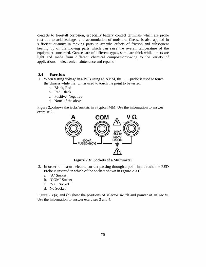
75
contacts to forestall corrosion, especially battery contact terminals which are prone rust due to acid leakages and accumulation of moisture. Grease is also applied in sufficient quantity in moving parts to avertthe effects of friction and subsequent heating up of the moving parts which can raise the overall temperature of the equipment concerned. Greases are of different types, some are thick while others are light and made from different chemical compositionsowing to the variety of applications in electronic maintenance and repairs. 2.4 Exercises 1. When testing voltage in a PCB using an AMM, the…….probe is used to touch
the chassis while the…….is used to touch the point to be tested. a. Black, Red b. Red, Black c. Positive, Negative d. None of the above
Figure 2.Xshows the jacks/sockets in a typical MM. Use the information to answer exercise 2.
Figure 2.X: Sockets of a Multimeter
2. In order to measure electric current passing through a point in a circuit, the RED Probe is inserted in which of the sockets shown in Figure 2.X1? a. ‘A’ Socket b. ‘COM’ Socket c. ‘VΩ’ Socket d. No Socket
Figure 2.Y(a) and (b) show the positions of selector switch and pointer of an AMM. Use the information to answer exercises 3 and 4.
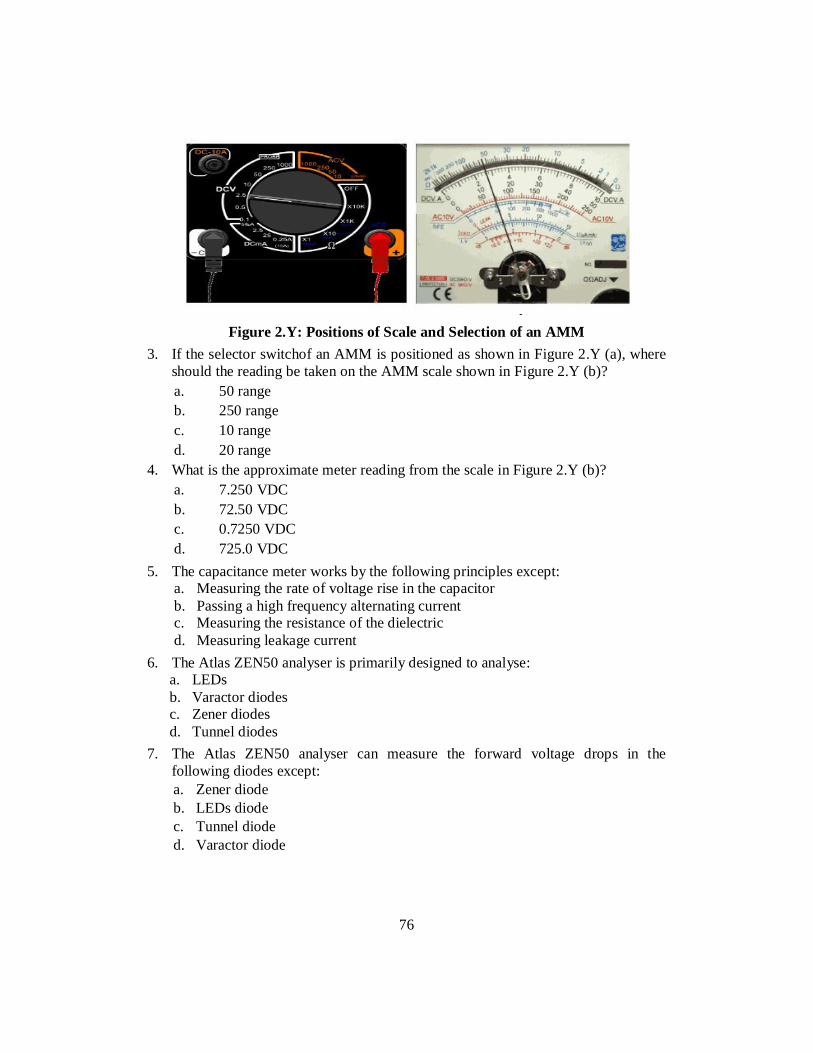
76
Figure 2.Y: Positions of Scale and Selection of an AMM
3. If the selector switchof an AMM is positioned as shown in Figure 2.Y (a), where should the reading be taken on the AMM scale shown in Figure 2.Y (b)? a. 50 range b. 250 range c. 10 range d. 20 range
4. What is the approximate meter reading from the scale in Figure 2.Y (b)? a. 7.250 VDC b. 72.50 VDC c. 0.7250 VDC d. 725.0 VDC
5. The capacitance meter works by the following principles except: a. Measuring the rate of voltage rise in the capacitor b. Passing a high frequency alternating current c. Measuring the resistance of the dielectric d. Measuring leakage current
6. The Atlas ZEN50 analyser is primarily designed to analyse: a. LEDs b. Varactor diodes c. Zener diodes d. Tunnel diodes
7. The Atlas ZEN50 analyser can measure the forward voltage drops in the following diodes except: a. Zener diode b. LEDs diode c. Tunnel diode d. Varactor diode
77
8. The ‘right’ tool used to clip off components’ leads and tails from the back of a PCB is: a. Cutter b. Side cutter c. End cutter d. Multi-wire cutter
9. Transistor tester can be used to determine: a. Reverse current b. Beta of the transistor c. Alpha of the transistor d. Forward current
10. In a Vectorscope, the standard analogue NTSC black is:
a. 7.5 IRE b. 75 IRE c. 0 IRE d. 100 IRE
11. Enumerate the procedure for using an IC Tester to check an IC. 12. What do you understand by oscilloscope? Explain how an oscilloscope can be
used and differentiate between an active, passive and ideal probe. 13. How can you power-up a signal generator and what is the function of the
following control knobs in the generator: (a) Power switch; (b)Setting adjustment knob; (c) Sine wave selection;(d) Modulation signal knob; (e) Amplitude offset adjustment knob.
14. Explain where Vectorscopes and Network Analyser can be useful. 15. Describe how to use a logic probe to diagnose a logic circuit.
78
CHAPTER THREE 3.0 PRACTICAL TROUBLESHOOTING TECHNIQUES The reader has learnt some of the test equipment, tools and materials that are useful or even necessary for effective electronic maintenance and repairs in the previous chapter. This chapter presents the common failures in electronic circuits, troubleshooting procedures and techniques as well as safety precautions to be observed in electronic maintenance and repairs that the reader is expected to learn. This is in preparation for practical maintenance and repair experiences to be discussed in Chapter Five. At the end of this chapter therefore, the reader should be able to explain: Common Symptomsand Failures in Electronic Equipment Practical Troubleshooting Techniques Safety Precautionsin Electronic Maintenance and Repairs
3.1 Common Symptomsand Failures in Electronic Equipment One of the most important skills necessary for effective electronic maintenance and repairs is the repairman/woman’s ability to quickly recognise failure and its associated symptoms in electronic circuits and components. Such failure can occur as a result of thermal expansion that can produce mechanical stresses which may cause material fatigue, especially when the thermal expansion coefficients of the materials that make up the component are different. Humidity and aggressive chemicals can cause corrosion of the packaging materials and leads, potentially breaking them and damaging the inside parts, leading to electrical failure. Exceeding the allowed environmental temperature range can cause overstressing of wire bonds, thus tearing the connections loose, cracking the semiconductor dies, or causing packaging cracks. Humidity, mechanical damage or shock and subsequent high temperature heating may also cause cracking in Printed Circuit Boards (PCBs).
Printed Circuit Board Failure: PCBs are vulnerable to environmental influences; for example, the traces are corrosion-prone and may be improperly etched leaving partial shorts, while the components’ terminals may be insufficiently plated through or filled with solder. The traces may crack under mechanical loads, often resulting in unreliable PCB operation. Residues of solder flux may facilitate corrosion; those of other materials on PCBs can cause electrical leaks. Polar covalent compounds can attract moisture like antistatic agents, forming a thin layer of conductive moisture between the traces; ionic compounds like chlorides tend to facilitate corrosion as shown in Figure 3.1.
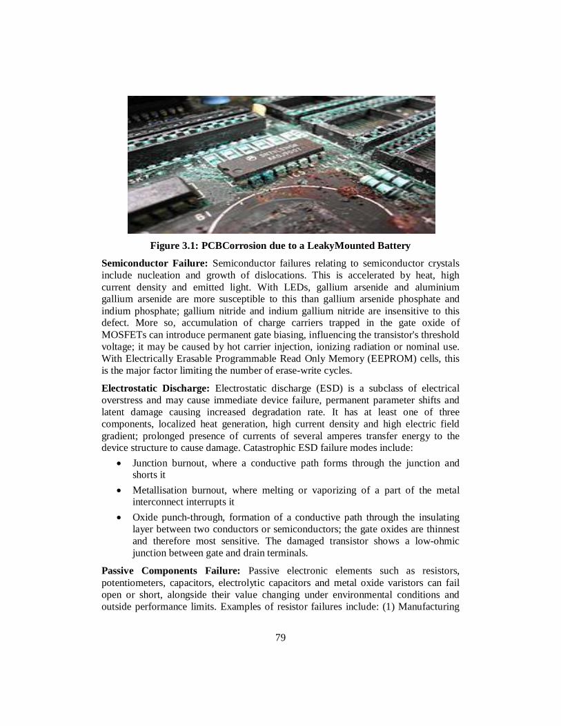
79
Figure 3.1: PCBCorrosion due to a LeakyMounted Battery
Semiconductor Failure: Semiconductor failures relating to semiconductor crystals include nucleation and growth of dislocations. This is accelerated by heat, high current density and emitted light. With LEDs, gallium arsenide and aluminium gallium arsenide are more susceptible to this than gallium arsenide phosphate and indium phosphate; gallium nitride and indium gallium nitride are insensitive to this defect. More so, accumulation of charge carriers trapped in the gate oxide of MOSFETs can introduce permanent gate biasing, influencing the transistor's threshold voltage; it may be caused by hot carrier injection, ionizing radiation or nominal use. With Electrically Erasable Programmable Read Only Memory (EEPROM) cells, this is the major factor limiting the number of erase-write cycles.
Electrostatic Discharge: Electrostatic discharge (ESD) is a subclass of electrical overstress and may cause immediate device failure, permanent parameter shifts and latent damage causing increased degradation rate. It has at least one of three components, localized heat generation, high current density and high electric field gradient; prolonged presence of currents of several amperes transfer energy to the device structure to cause damage. Catastrophic ESD failure modes include:
Junction burnout, where a conductive path forms through the junction and shorts it
Metallisation burnout, where melting or vaporizing of a part of the metal interconnect interrupts it
Oxide punch-through, formation of a conductive path through the insulating layer between two conductors or semiconductors; the gate oxides are thinnest and therefore most sensitive. The damaged transistor shows a low-ohmic junction between gate and drain terminals.
Passive Components Failure: Passive electronic elements such as resistors, potentiometers, capacitors, electrolytic capacitors and metal oxide varistors can fail open or short, alongside their value changing under environmental conditions and outside performance limits. Examples of resistor failures include: (1) Manufacturing
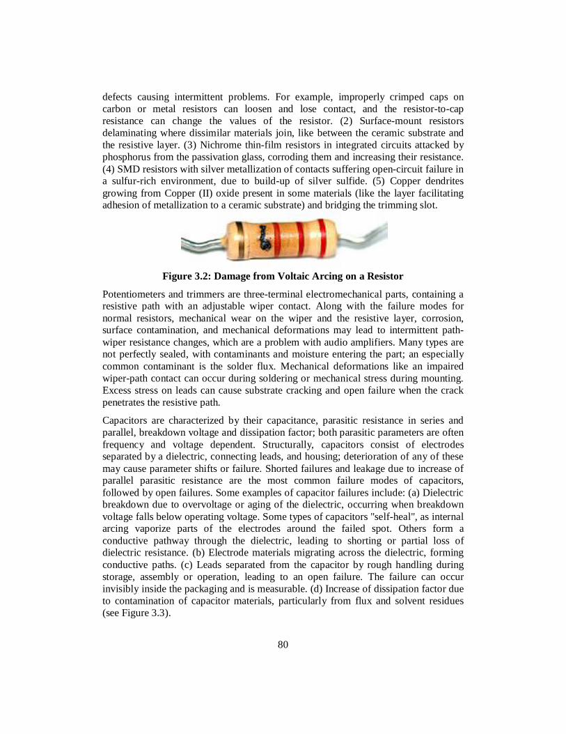
80
defects causing intermittent problems. For example, improperly crimped caps on carbon or metal resistors can loosen and lose contact, and the resistor-to-cap resistance can change the values of the resistor. (2) Surface-mount resistors delaminating where dissimilar materials join, like between the ceramic substrate and the resistive layer. (3) Nichrome thin-film resistors in integrated circuits attacked by phosphorus from the passivation glass, corroding them and increasing their resistance. (4) SMD resistors with silver metallization of contacts suffering open-circuit failure in a sulfur-rich environment, due to build-up of silver sulfide. (5) Copper dendrites growing from Copper (II) oxide present in some materials (like the layer facilitating adhesion of metallization to a ceramic substrate) and bridging the trimming slot.
Figure 3.2: Damage from Voltaic Arcing on a Resistor
Potentiometers and trimmers are three-terminal electromechanical parts, containing a resistive path with an adjustable wiper contact. Along with the failure modes for normal resistors, mechanical wear on the wiper and the resistive layer, corrosion, surface contamination, and mechanical deformations may lead to intermittent path-wiper resistance changes, which are a problem with audio amplifiers. Many types are not perfectly sealed, with contaminants and moisture entering the part; an especially common contaminant is the solder flux. Mechanical deformations like an impaired wiper-path contact can occur during soldering or mechanical stress during mounting. Excess stress on leads can cause substrate cracking and open failure when the crack penetrates the resistive path.
Capacitors are characterized by their capacitance, parasitic resistance in series and parallel, breakdown voltage and dissipation factor; both parasitic parameters are often frequency and voltage dependent. Structurally, capacitors consist of electrodes separated by a dielectric, connecting leads, and housing; deterioration of any of these may cause parameter shifts or failure. Shorted failures and leakage due to increase of parallel parasitic resistance are the most common failure modes of capacitors, followed by open failures. Some examples of capacitor failures include: (a) Dielectric breakdown due to overvoltage or aging of the dielectric, occurring when breakdown voltage falls below operating voltage. Some types of capacitors "self-heal", as internal arcing vaporize parts of the electrodes around the failed spot. Others form a conductive pathway through the dielectric, leading to shorting or partial loss of dielectric resistance. (b) Electrode materials migrating across the dielectric, forming conductive paths. (c) Leads separated from the capacitor by rough handling during storage, assembly or operation, leading to an open failure. The failure can occur invisibly inside the packaging and is measurable. (d) Increase of dissipation factor due to contamination of capacitor materials, particularly from flux and solvent residues (see Figure 3.3).
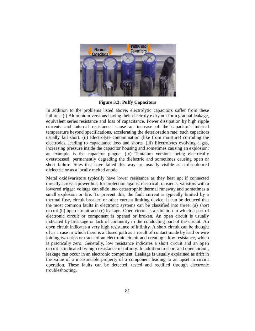
81
Figure 3.3: Puffy Capacitors
In addition to the problems listed above, electrolytic capacitors suffer from these failures: (i) Aluminium versions having their electrolyte dry out for a gradual leakage, equivalent series resistance and loss of capacitance. Power dissipation by high ripple currents and internal resistances cause an increase of the capacitor's internal temperature beyond specifications, accelerating the deterioration rate; such capacitors usually fail short. (ii) Electrolyte contamination (like from moisture) corroding the electrodes, leading to capacitance loss and shorts. (iii) Electrolytes evolving a gas, increasing pressure inside the capacitor housing and sometimes causing an explosion; an example is the capacitor plague. (iv) Tantalum versions being electrically overstressed, permanently degrading the dielectric and sometimes causing open or short failure. Sites that have failed this way are usually visible as a discoloured dielectric or as a locally melted anode.
Metal oxidevaristors typically have lower resistance as they heat up; if connected directly across a power bus, for protection against electrical transients, varistors with a lowered trigger voltage can slide into catastrophic thermal runaway and sometimes a small explosion or fire. To prevent this, the fault current is typically limited by a thermal fuse, circuit breaker, or other current limiting device. It can be deduced that the most common faults in electronic systems can be classified into three: (a) short circuit (b) open circuit and (c) leakage. Open circuit is a situation in which a part of electronic circuit or component is opened or broken. An open circuit is usually indicated by breakage or lack of continuity in the conducting part of the circuit. An open circuit indicates a very high resistance of infinity. A short circuit can be thought of as a case in which there is a closed path as a result of contact made by lead or wire joining two trips or tracts of an electronic circuit and creating a low resistance, which is practically zero. Generally, low resistance indicates a short circuit and an open circuit is indicated by high resistance of infinity. In addition to short and open circuit, leakage can occur in an electronic component. Leakage is usually explained as drift in the value of a measureable property of a component leading to an upset in circuit operation. These faults can be detected, tested and rectified through electronic troubleshooting.
82
3.2 Practical Troubleshooting Techniques The first step in electronic troubleshooting is to carry out preliminary check and when technicians are doing this they should know: All about relevant safety issues All about relevant regulatory issues (environmental impact laws, codes etc) What is normal behaviour About various modes of operation (automatic modes, programming modes,
etc) What the various parts of a system do What the controls are supposed to do What inputs and outputs are for and how they should be connected Whether a device can be reasonably tested when it is removed from a system What role software might play in performance
When the preliminary checks are completed and the unit is still not working, the next thing to do is a visual inspection of the interior of the equipment. When doing this, the technician is expected to look out for the following: (1) Burned and decoloured components (2) Broken wires and components (3) Cracked or burned circuit boards (4) Foreign objects (papers, clips screws etc) (5) Bent transistors leads that may be touching (this includes other non-insulated leads as well) (6) Parts falling out of sockets or only partly seated and (7) Loose or partly seated connectors. When the preliminary visual inspection is completed, a preliminary electrical check should be carried out. This involves checking for overheating of components and verifying the power-supply voltage. Hot electronic components often give off a distinct odour; therefore, the nose may give important information. The finger may also be used to check for excessive heat in accomplishing the troubleshooting task. If symptoms of the failure are still eminent then a more elaborate procedure ortechnique needs to be followed.
There are many tasks and procedures that can be taken in carrying out electronictroubleshooting which will help in isolating faults or problems to one stage. Some experts refer to these measurements as troubleshooting techniques. Some of these techniques include: (a) the symptom-function technique, (b) the signal-tracing technique, (c) measuring voltage and resistance technique, and (d) the substitution technique. The problem very often, is to decide which technique will be suitable in troubleshooting the defect, particularly if how the trouble is caused and what causes it is not known.
The symptom-function technique may be the first technique to be used in troubleshooting in order to isolate the defect to a particular portion of a piece of electronic equipment. In troubleshooting electronic equipment with the symptom-function technique, the relationship between the symptoms, the functions and the
Related Documents


