INTERNATIONAL RESEARCH JOURNAL OF TECHNOLOGY AND APPLIED SCIENCE http://www.irjtas.com (An ISO Certified journal) VOL. 1 Issue 1 January 17 Copyright to IRJTAS DOI: 10.17001/ IRJTAS.2017. 0809001 A Highly Efficient Lector Technique for Power Reduction in C-MOS Circuit Siddharth Singh (M.tech Scholar), Prof. Sachin Bandewar (Assistant Professor) E-mail – [email protected] 1 , [email protected] 2 Dept. of Electronic &Communications Engineering 1, 2 , branch (VLSI) SSSCE R.K.D.F. University Bhopal (M.P.) INDIA. Abstract: At whatever point we need to create computerized incorporated circuits, then we are confronting a test by higher power utilization. The blend of more noteworthy useful reconciliation, higher clock speeds and littler process geometries have added to huge development in power thickness. With the assistance of scaling we enhance usefulness on a chip, and transistor thickness. Scaling can likewise expand speed and recurrence of operation and subsequently higher execution [1]. There are a few methods that can be utilized to lessen spillage control in productive way yet the fundamental burden of every innovation that constrains the use of every system. In our base paper Dynamic CMOS circuits are fundamentally utilized as a part of superior huge scale incorporated (VLSI) frameworks. Furthermore, here we are ascertaining static clamor edge and in addition commotion investigation of this technique However; they experience the ill effects of confinements, for example, clamor resilience, charge spillage, and power utilization. Be that as it may, in that paper they can disregarded static power scattering [1][2]. Static power has turned into an incredible test for present and future advances. There are many purposes behind which control misfortunes happen in CMOS circuit. 1) Sub-limit spillage (frail reversal current) 2.)Gate oxide spillage (Tunneling current 3.) Channel punch through 4.) Drain prompted obstruction bringing down. Presently, we can have presented an approach that can diminish the static power scattering and spillage control dissemination of the circuit. As voltages scale descending with the geometries limit voltages should likewise lessening to pick up the execution focal points of the new innovation however spillage current increments exponentially. More slender door oxides have prompted to an expansion in entryway spillage current. Presently a day spillage control has turned into an undeniably critical issue. With the primary segment of spillage [3], the sub-limit current, exponentially expanding with diminishing gadget measurements, spillage charges a steadily expanding offer in the processor control utilization. In 65 nm and underneath innovations, spillage represents 30-40% of processor power. As indicated by the International Technology Roadmap for Semiconductors (ITRS), spillage control dissemination may in the long run command add up to power utilization as innovation highlight sizes contract. While there are such a large number of procedures innovation and circuit-level arrangements that can be utilized to diminished spillage. Presently, we proposed a technique that can used to lessen both spillage and element control with least required zone and deferral [4]. Keywords: CMOS, Micro-wind 3.0.Leakage Power, Sub-threshold Leakage, Threshold voltage.

Welcome message from author
This document is posted to help you gain knowledge. Please leave a comment to let me know what you think about it! Share it to your friends and learn new things together.
Transcript

INTERNATIONAL RESEARCH JOURNAL OF TECHNOLOGY AND APPLIED SCIENCE
http://www.irjtas.com (An ISO Certified journal)
VOL. 1 Issue 1 January 17
Copyright to IRJTAS DOI: 10.17001/ IRJTAS.2017. 0809001
A Highly Efficient Lector Technique for Power Reduction in
C-MOS Circuit
Siddharth Singh (M.tech Scholar), Prof. Sachin Bandewar (Assistant Professor)
E-mail – [email protected], [email protected]
Dept. of Electronic &Communications Engineering1, 2, branch (VLSI)
SSSCE R.K.D.F. University Bhopal (M.P.) INDIA.
Abstract: At whatever point we need to create computerized incorporated circuits, then we are
confronting a test by higher power utilization. The blend of more noteworthy useful reconciliation,
higher clock speeds and littler process geometries have added to huge development in power thickness.
With the assistance of scaling we enhance usefulness on a chip, and transistor thickness. Scaling can
likewise expand speed and recurrence of operation and subsequently higher execution [1]. There are a
few methods that can be utilized to lessen spillage control in productive way yet the fundamental
burden of every innovation that constrains the use of every system. In our base paper Dynamic CMOS
circuits are fundamentally utilized as a part of superior huge scale incorporated (VLSI) frameworks.
Furthermore, here we are ascertaining static clamor edge and in addition commotion investigation of
this technique However; they experience the ill effects of confinements, for example, clamor resilience,
charge spillage, and power utilization. Be that as it may, in that paper they can disregarded static power
scattering [1][2]. Static power has turned into an incredible test for present and future advances. There
are many purposes behind which control misfortunes happen in CMOS circuit. 1) Sub-limit spillage
(frail reversal current) 2.)Gate oxide spillage (Tunneling current 3.) Channel punch through 4.) Drain
prompted obstruction bringing down.
Presently, we can have presented an approach that can diminish the static power scattering and spillage
control dissemination of the circuit. As voltages scale descending with the geometries limit voltages
should likewise lessening to pick up the execution focal points of the new innovation however spillage
current increments exponentially. More slender door oxides have prompted to an expansion in
entryway spillage current. Presently a day spillage control has turned into an undeniably critical issue.
With the primary segment of spillage [3], the sub-limit current, exponentially expanding with
diminishing gadget measurements, spillage charges a steadily expanding offer in the processor control
utilization. In 65 nm and underneath innovations, spillage represents 30-40% of processor power. As
indicated by the International Technology Roadmap for Semiconductors (ITRS), spillage control
dissemination may in the long run command add up to power utilization as innovation highlight sizes
contract. While there are such a large number of procedures innovation and circuit-level arrangements
that can be utilized to diminished spillage. Presently, we proposed a technique that can used to lessen
both spillage and element control with least required zone and deferral [4].
Keywords: CMOS, Micro-wind 3.0.Leakage Power, Sub-threshold Leakage, Threshold voltage.

INTERNATIONAL RESEARCH JOURNAL OF TECHNOLOGY AND APPLIED SCIENCE
http://www.irjtas.com (An ISO Certified journal)
VOL. 1 Issue 1 January 17
Copyright to IRJTAS DOI: 10.17001/ IRJTAS.2017. 0809001
I. INTRODUCTION
In history of CMOS plan, behind the speed and region of any chip, control scattering or power
utilization was optional thought.
In any case, be that as it may we are expanding the aggregate number of transistors and check
recurrence in a solitary chip, then power utilization comes in intense issue [4][5]. Quick power
drawn by any chip from the power supply is straightforwardly relative to the duplication of
supply voltage V(t) and supply current Idd(t).
P(t) = Idd(t)*v(t)
Presently, add up to vitality expended over some time interim T is, here are for the most part
two segments that set up the measure of force dissemination in a CMOS circuit, for example,
1) Static power dissipation: Static power dispersal: Due to sub-limit conduction, tunneling current
through entryway oxide, Leakage through turn around one-sided diodes [6].
2) Dynamic power dissipation: Due to charging and discharging of load capacitances “Short circuit”
current while both PMOS and NMOS networks are partially “ON” [7].

INTERNATIONAL RESEARCH JOURNAL OF TECHNOLOGY AND APPLIED SCIENCE
http://www.irjtas.com (An ISO Certified journal)
VOL. 1 Issue 1 January 17
Copyright to IRJTAS DOI: 10.17001/ IRJTAS.2017. 0809001
Static power dissipation: -For static power dissemination we are thinking about the Static
CMOS inverter which is appeared in figure [8][9].
In the event that the input=0, the related NMOS transistor is OFF and the PMOS transistor
is ON. The yield voltage is Vdd or rationale 1. At the point when the info =1 the related
NMOS transistor is ON and the PMOS transistor is OFF. The yield voltage is 0 volt. Take
note of that one transistor is constantly OFF when the entryway is in both of these rationale
states [9]. In a perfect world, no present courses through the Off transistor so the power
dispersal is zero when the circuit is peaceful. Zero tranquil power scattering is a main
preferred standpoint of CMOS over contending transistor advancements. Be that as it may,
optional impacts including sub-limit conduction, burrowing and spillage prompt to little
measure of static current moving through the "OFF" transistor. Expecting the spillage
current is steady so quick and normal power are the same; the static power dissemination is
the result of aggregate spillage current and the supply voltage [10].
Pstatic = Istatic * Vdd
There is some little static scattering because of invert predisposition spillage between
dissemination district and the substrate. Moreover, sub-limit conduction can add to the
static dissemination. Presently we are presented a model where we demonstrate that the
parasitic diode is appeared between n-well and substrate [10][11]. Since parasitic diodes are
turn around one-sided then just spillage current adds to static power scattering. The spillage
current is portrayed by the diode condition [11].

INTERNATIONAL RESEARCH JOURNAL OF TECHNOLOGY AND APPLIED SCIENCE
http://www.irjtas.com (An ISO Certified journal)
VOL. 1 Issue 1 January 17
Copyright to IRJTAS DOI: 10.17001/ IRJTAS.2017. 0809001
II. PROBLEM STATEMENT
This examination work is titled for to build up the region productive VLSI configuration by
decreasing the static power through LACTOR system. While planning a VLSI framework
control dissemination is a standout amongst the most vital issue [12]. Presently, up to a
specific time dynamic power was the single biggest concern yet however the innovation
highlight size psychologist's static power has turned into an imperative issue as dynamic power
[13]. An outstanding past system called the rest transistor method cuts off Vdd as well as GND
associations of transistors to spare spillage control utilization. Be that as it may, when
transistors are permitted to glide, a framework may need to hold up quite a while to
dependably reestablish lost state and subsequently may encounter truly debased execution.
Along these lines, holding state is significant for a framework that requires quick reaction even
while in an inert state. The two basic methodologies are lethargic stack and tired manager.
Both strategies are fabulous in such manner. The static and element force of lethargic stack is
significantly low. Yet, it has a postpone punishment and its zone prerequisite is most extreme
contrasted and different procedures. Again the tired guardian prepare has incredible speed
criteria yet it requires more static and element control than sluggish stack. We will likely
tradeoff between these confinements and along these lines proposes new strategies which
decrease both spillage and element control with least conceivable territory and defer exchange
off.
III.MOTIVATION
V = diode voltage
Q= charge of electron (1.602*10-19c)
K= Boltzmann’s constant (1038*10-23)
T = temperature
The static power dissemination is the result of the devise spillage current and the power supply
voltage [13].
CMOS Technology was one of the standards of VLSI Design. In 0.18u or more innovation
Dynamic power is one of the primary variables of aggregate power utilization. Be that as it
may, when innovation includes measure psychologists to .13u and beneath innovation static

INTERNATIONAL RESEARCH JOURNAL OF TECHNOLOGY AND APPLIED SCIENCE
http://www.irjtas.com (An ISO Certified journal)
VOL. 1 Issue 1 January 17
Copyright to IRJTAS DOI: 10.17001/ IRJTAS.2017. 0809001
(Leakage) control rules the dynamic power. So be that as it may, the planners proposed a few
techniques to lessen the spillage [14].
In Base Technique there is a no strategy for power decrease yet it spares the state and
additionally least zone and postponement. Rest Transistor Technique is most normal strategy
for accomplishing ultra-low spillage however it decimates the state and additionally expanding
deferrals and range. Constrained stack strategy is another technique and it can spare the state.
Be that as it may, in this procedure Dynamic Power utilization is increments and it can't utilize
high Vth immediately. By brushing these two methods Sleepy Stack methodologies is
proposed. It lessens the spillage comparatively like rest transistor method yet the fundamental
favorable position over rest transistor system is spare the rationale state. In addition, Sleepy
Stack approach accompanies region and postpone overhead and slower strategy than other
procedure. Be that as it may, Sleepy Keeper methodologies are truly calculable for
proliferation postponement and static power exhibitions. Albeit, Sleepy Keeper approaches
brings about territory and element control dissemination. UT still now this two normal strategy
is utilized.
Hence we sought a new method which can have excellent tradeoff between power, area, and
delay.
IV. PLAN CRITERIA
In present time we are for the most part utilizing CMOS Technology as a result of its
expending less power. Yet, time by time when innovation include estimate shrivel sub-
edge spillage current is increments as the decline of edge voltage. In this outline model
we concentrated on sub edge spillage control utilization furthermore centered on body

INTERNATIONAL RESEARCH JOURNAL OF TECHNOLOGY AND APPLIED SCIENCE
http://www.irjtas.com (An ISO Certified journal)
VOL. 1 Issue 1 January 17
Copyright to IRJTAS DOI: 10.17001/ IRJTAS.2017. 0809001
biasing impact. At last, we clarify the exchanging force and defer exchange off of non
specific CMOS circuit.
V. LEAKAGE
At whatever point we are utilizing 0.18u or more innovation then element power is the
overwhelming component however at whatever point we are utilizing 0.13u and
beneath innovation then another predominant variable will be happened that is called
static power for power utilization [15]. One of the principle benefactors for the static
power utilization is sub-edge spillage current which is appeared in the Figure.
3.1(a) i.e., the deplete to source current when the entryway voltage is little as contrast
with edge voltage. At the point when the extent of the gadgets is diminishing then sub-
edge spillage current is increments exponentially as the reduction of limit voltage.
Stacking transistor can decrease sub-edge spillage. So it is called stacked impact.
Where at least two stacked transistors is killed together, the outcome can lessen the
spillage control [14][15]. For killed the single transistor in Figure 1.4 spillage current
Isub0 can be communicated as takes after:
n=sub-limit coefficient V= warm voltage Vgs0, Vth0, Vbs0 and Vds0 are the entryway
to-source voltage, the zero-predisposition edge voltage, the base - to-source voltage and
the deplete to-source voltage separately. is the body-predisposition impact coefficient,
and is the Drain Induced Barrier Lowering (DIBL) coefficient. µ is zero-predisposition
portability, Cox is the door oxide capacitance, W is the width of the transistor, and Leff
is the successful channel length. (Take note of that all through this venture we accept
µn = 2µp, i.e., NMOS bearer versatility is twice PMOS transporter portability).
Likewise take note of that we utilize a W/L proportion in view of a real transistor
estimate, in which way a W/L proportion legitimately describes circuit models utilized
as a part of this case. In Figure two transistor are killed together (M1=M2). Along these
lines, where Vex is the voltage at the hub amongst M1 and M2, and n coefficient will
be increment as the innovation include estimate recoils. Edge voltage can be controlled
by body predisposition impact [16].
Changing the substrate voltage makes the limit voltage change. So the distinctive sort
of impact is emerging for changing the substrate voltage like Zero-Body Bias, Reverse-
Body Bias and Forward-Body Bias. This Phenomenon is as often as possible utilized
for controlling the limit voltage. Consistent subject to the transistor parameter and the
INTERNATIONAL RESEARCH JOURNAL OF TECHNOLOGY AND APPLIED SCIENCE
http://www.irjtas.com (An ISO Certified journal)
VOL. 1 Issue 1 January 17
Copyright to IRJTAS DOI: 10.17001/ IRJTAS.2017. 0809001
innovation include estimate. By controlling body biasing impact with changing the
consistent term we can undoubtedly control the spillage control [15].
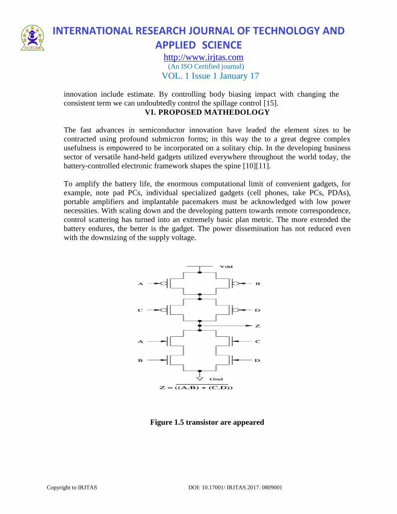
VI. PROPOSED MATHEDOLOGY
The fast advances in semiconductor innovation have leaded the element sizes to be
contracted using profound submicron forms; in this way the to a great degree complex
usefulness is empowered to be incorporated on a solitary chip. In the developing business
sector of versatile hand-held gadgets utilized everywhere throughout the world today, the
battery-controlled electronic framework shapes the spine [10][11].
To amplify the battery life, the enormous computational limit of convenient gadgets, for
example, note pad PCs, individual specialized gadgets (cell phones, take PCs, PDAs),
portable amplifiers and implantable pacemakers must be acknowledged with low power
necessities. With scaling down and the developing pattern towards remote correspondence,
control scattering has turned into an extremely basic plan metric. The more extended the
battery endures, the better is the gadget. The power dissemination has not reduced even
with the downsizing of the supply voltage.
Figure 1.5 transistor are appeared
INTERNATIONAL RESEARCH JOURNAL OF TECHNOLOGY AND APPLIED SCIENCE
http://www.irjtas.com (An ISO Certified journal)
VOL. 1 Issue 1 January 17
Copyright to IRJTAS DOI: 10.17001/ IRJTAS.2017. 0809001
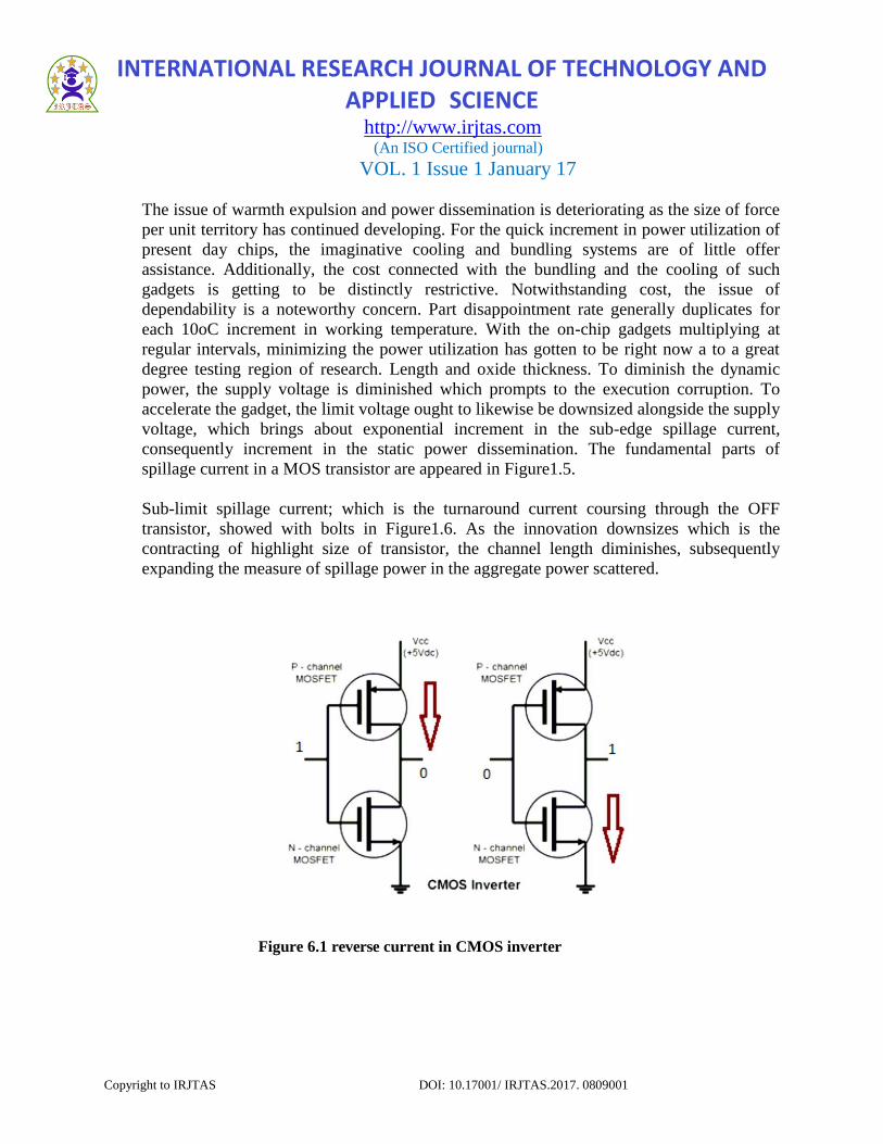
The issue of warmth expulsion and power dissemination is deteriorating as the size of force
per unit territory has continued developing. For the quick increment in power utilization of
present day chips, the imaginative cooling and bundling systems are of little offer
assistance. Additionally, the cost connected with the bundling and the cooling of such
gadgets is getting to be distinctly restrictive. Notwithstanding cost, the issue of
dependability is a noteworthy concern. Part disappointment rate generally duplicates for
each 10oC increment in working temperature. With the on-chip gadgets multiplying at
regular intervals, minimizing the power utilization has gotten to be right now a to a great
degree testing region of research. Length and oxide thickness. To diminish the dynamic
power, the supply voltage is diminished which prompts to the execution corruption. To
accelerate the gadget, the limit voltage ought to likewise be downsized alongside the supply
voltage, which brings about exponential increment in the sub-edge spillage current,
consequently increment in the static power dissemination. The fundamental parts of
spillage current in a MOS transistor are appeared in Figure1.5.
Sub-limit spillage current; which is the turnaround current coursing through the OFF
transistor, showed with bolts in Figure1.6. As the innovation downsizes which is the
contracting of highlight size of transistor, the channel length diminishes, subsequently
expanding the measure of spillage power in the aggregate power scattered.
Figure 6.1 reverse current in CMOS inverter
INTERNATIONAL RESEARCH JOURNAL OF TECHNOLOGY AND APPLIED SCIENCE
http://www.irjtas.com (An ISO Certified journal)
VOL. 1 Issue 1 January 17
Copyright to IRJTAS DOI: 10.17001/ IRJTAS.2017. 0809001
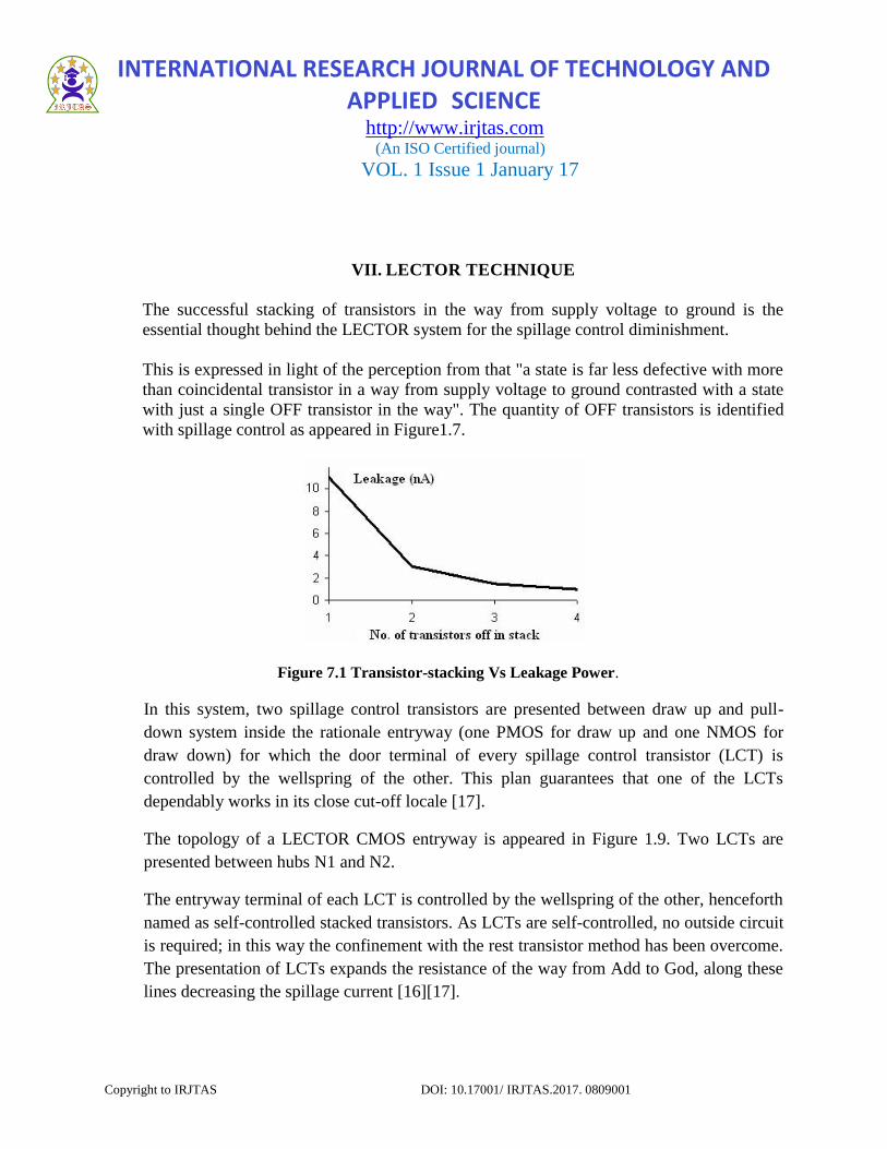
VII. LECTOR TECHNIQUE
The successful stacking of transistors in the way from supply voltage to ground is the
essential thought behind the LECTOR system for the spillage control diminishment.
This is expressed in light of the perception from that "a state is far less defective with more
than coincidental transistor in a way from supply voltage to ground contrasted with a state
with just a single OFF transistor in the way". The quantity of OFF transistors is identified
with spillage control as appeared in Figure1.7.
Figure 7.1 Transistor-stacking Vs Leakage Power.
In this system, two spillage control transistors are presented between draw up and pull-
down system inside the rationale entryway (one PMOS for draw up and one NMOS for
draw down) for which the door terminal of every spillage control transistor (LCT) is
controlled by the wellspring of the other. This plan guarantees that one of the LCTs
dependably works in its close cut-off locale [17].
The topology of a LECTOR CMOS entryway is appeared in Figure 1.9. Two LCTs are
presented between hubs N1 and N2.
The entryway terminal of each LCT is controlled by the wellspring of the other, henceforth
named as self-controlled stacked transistors. As LCTs are self-controlled, no outside circuit
is required; in this way the confinement with the rest transistor method has been overcome.
The presentation of LCTs expands the resistance of the way from Add to God, along these
lines decreasing the spillage current [16][17].

INTERNATIONAL RESEARCH JOURNAL OF TECHNOLOGY AND APPLIED SCIENCE
http://www.irjtas.com (An ISO Certified journal)
VOL. 1 Issue 1 January 17
Copyright to IRJTAS DOI: 10.17001/ IRJTAS.2017. 0809001
Figure 7.2 LECTOR CMOS Gate
Spillage Control Transistor (LECTOR) procedure is represented in detail with the instance
of an inverter. A LECTOR INVERTER is appeared in Figure 1.9. A PMOS is presented as
LCT1 and a NMOS as LCT2 amongst N1 and N2 hubs of inverter. The yield of inverter is
taken from the associated deplete hubs LCT1 and LCT2.

INTERNATIONAL RESEARCH JOURNAL OF TECHNOLOGY AND APPLIED SCIENCE
http://www.irjtas.com (An ISO Certified journal)
VOL. 1 Issue 1 January 17
Copyright to IRJTAS DOI: 10.17001/ IRJTAS.2017. 0809001
Figure 8.1 input LCT NAND
The source hubs of LCT1 and LCT2 are the hubs N1 and N2 separately of the draw up and
the draw down rationale. The doors of LCT1 and LCT2 are controlled by the potential at
source terminal of LCT2 and LCT1 individually. This association dependably keeps one of
the two LCTs in its close cut-off district for any information [16][17].
At the point when Add = 1V, input A = 0, the voltage at the hub N2 is 800 mV. LCT1 can't
be totally killed as the voltage is not adequate. Subsequently, the LCT1 resistance will be
close to yet marginally lesser than it's OFF resistance, permitting conduction. The
resistance gave by LCT1, despite the fact that not equivalent to the OFF resistance,
expands the resistance in the way of supply voltage to ground, in this manner diminishing
the sub-limit spillage current, accomplishing lessening in spillage control. Essentially,
when input A = 1, the voltage at the hub N1 is 200 mV; thus LCT2 will be worked in close
cut-off state. The conditions of the considerable number of transistors in the LECTOR
inverter for every conceivable info are classified in Table I [13][12].
INTERNATIONAL RESEARCH JOURNAL OF TECHNOLOGY AND APPLIED SCIENCE
http://www.irjtas.com (An ISO Certified journal)
VOL. 1 Issue 1 January 17
Copyright to IRJTAS DOI: 10.17001/ IRJTAS.2017. 0809001
Figure 7.3 LECTOR based CMOS Inverter
The reenactment waveforms of LECTOR NAND from Figure 1.11 demonstrate that the
essential qualities of NAND are held by LECTOR NAND. Alongside the resistance in the
way, the proliferation deferral of the entryway likewise gets expanded. The transistors of
LCT inverter are estimated with the end goal that the spread deferral is diminished or
equivalent to its base case. In the rest related system, the rest transistors must have the
capacity to detach the power supply as well as ground from whatever is left of the
transistors of the door. Consequently, they should be made bulkier disseminating more
dynamic power. This balances the reserve funds yielded when the circuit is sit out of gear.
Rest transistor system relies on upon info vector and it needs extra hardware to screen and
control the exchanging of rest transistors, devouring force in both dynamic and sit still
states. In correlation, LECTOR creates the required control motions inside the entryway
and is additionally vector free. Two transistors are included LECTOR procedure in each
way from Vdid to GND regardless of number of transistors in draw up and pull-down
system.
While, constrained stacks have 100% zone overhead. The stacking prerequisite with LCTs
is a consistent which is much lower. While, the stacking prerequisites with constrained
stacks rely on upon number of transistors included and are enormous. Henceforth, the
execution corruption is inconsequential on account of LECTOR, and we defeat the
disadvantage confronted by constrained stack strategy
VII. APPLYING LECTOR TO CMOS CIRCUITS
Different circuit uses of the LECTOR system are investigated in this segment. The
LECTOR method is connected to the accompanying CMOS circuits furthermore their
individual base case is executed to figure the measure of spillage power diminished in
LECTOR procedure.
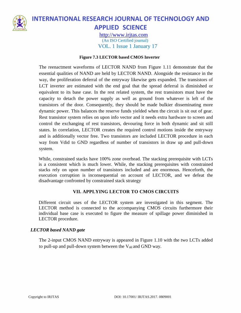
LECTOR based NAND gate
The 2-input CMOS NAND entryway is appeared in Figure 1.10 with the two LCTs added
to pull-up and pull-down system between the Vdd and GND way.
INTERNATIONAL RESEARCH JOURNAL OF TECHNOLOGY AND APPLIED SCIENCE
http://www.irjtas.com (An ISO Certified journal)
VOL. 1 Issue 1 January 17
Copyright to IRJTAS DOI: 10.17001/ IRJTAS.2017. 0809001
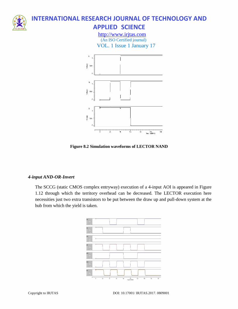
Figure 8.2 Simulation waveforms of LECTOR NAND
4-input AND-OR-Invert
The SCCG (static CMOS complex entryway) execution of a 4-input AOI is appeared in Figure
1.12 through which the territory overhead can be decreased. The LECTOR execution here
necessities just two extra transistors to be put between the draw up and pull-down system at the
hub from which the yield is taken.

INTERNATIONAL RESEARCH JOURNAL OF TECHNOLOGY AND APPLIED SCIENCE
http://www.irjtas.com (An ISO Certified journal)
VOL. 1 Issue 1 January 17
Copyright to IRJTAS DOI: 10.17001/ IRJTAS.2017. 0809001
Figure 8.3 Four input AOI
The entryway level schematic of 4:1 multiplexer is appeared in Figure 1.14. The LECTOR
usage includes the expansion of two LCTs in every door between the supply and ground
way.
Through the reenactment waveforms appeared in Figure 1.13 the qualities of LECTOR AOI
look like the base case.
4:1 Multiplexer
Fig. 8.6 Simulation waveforms for LECTOR MUX
Figure 8.5 4:1 Multiplexer

INTERNATIONAL RESEARCH JOURNAL OF TECHNOLOGY AND APPLIED SCIENCE
http://www.irjtas.com (An ISO Certified journal)
VOL. 1 Issue 1 January 17
Copyright to IRJTAS DOI: 10.17001/ IRJTAS.2017. 0809001
The reenactment waveform appeared in Figure 8.4 speaks to the LECTOR Multiplexer
through which it can be watched that its qualities look like that of the routine case.
Full Adder
Figure 8.7 A Full Adder
Figure 8.8 Simulation waveforms for LECTOR Full Adder
The Gate level schematic of Full Adder is appeared in Figure 1.16. The LECTOR usage includes
the expansion of two LCTs for every door. The transistor level schematic for ex-or entryways is
like that of And-Or-Invert.

INTERNATIONAL RESEARCH JOURNAL OF TECHNOLOGY AND APPLIED SCIENCE
http://www.irjtas.com (An ISO Certified journal)
VOL. 1 Issue 1 January 17
Copyright to IRJTAS DOI: 10.17001/ IRJTAS.2017. 0809001
There are 4 conceivable blends for 2-input NAND, thus the normal of the four power dispersals
gives the spillage control. On account of 4-info AOI, control dispersals relating to all the 16 blends
are arrived at the midpoint of. For Multiplexer, the normal of 64 power disseminations is viewed
as and for full viper, the normal of 8 power dispersals is thought to be as the static power scattered.
For every situation, the spillage power is measured by energizing both the circuits (Conventional
and LECTOR) with same arrangement of information vectors.
The reenactment waveforms for full snake as appeared in Figure 1.17, looks like the qualities of
routine full viper.
IX. EXPERIMENTAL RESULTS
The spillage power is measured utilizing the HSPICE test system. The outcomes got through the
system for 2-input NAND door is appeared in Table III. Reproduction for the 2-input NAND is
performed by taking four diverse process parameters Viz. 180nm, 90nm, 65nm and 45nm.
The supply voltages to be considered for the four procedure parameters (innovations) alongside
the edge voltages for NMOS and PMOS in the particular advancements are as appeared in Table
II.
Spillage control dissemination is taken as the normal of force dispersals got at all the possible
input vectors of CMOS circuit.
X. REMARK
The expansion in spillage control in light of the downsizing of gadget measurements, supply and
limit voltages to accomplish elite and low element control dissemination, turns out to be more with
the profound submicron and Nano-meter advancements and in this manner it turns into an
incredible test to handle the issue of spillage power. LECTOR utilizes two LCTs which are self-

INTERNATIONAL RESEARCH JOURNAL OF TECHNOLOGY AND APPLIED SCIENCE
http://www.irjtas.com (An ISO Certified journal)
VOL. 1 Issue 1 January 17
Copyright to IRJTAS DOI: 10.17001/ IRJTAS.2017. 0809001
controlled transistors. LECTOR accomplishes the decrease in spillage control like other spillage
lessening strategies, for example, tired stack, tired attendant, and so on., alongside the benefit of
not influencing the dynamic power, since this strategy does not require any extra control and
screen hardware furthermore in this system, the correct rationale state is kept up. The LECTOR
procedure when connected to nonexclusive rationale circuits accomplishes up to 40-45% spillage
lessening over the particular ordinary circuits without influencing the dynamic power. A tradeoff
between Propagation postponement and range overhead exists here as the defer lessening by
estimating the transistors will expand the territory overhead.
XI. CONCLUSIONS
The expansion in spillage control in view of the downsizing of gadget measurements, supply and
limit voltages keeping in mind the end goal to accomplish superior and low element control
scattering, turns out to be more with the profound submicron and Nano meter advances and
consequently it turns into an extraordinary test to handle the issue of spillage power. LCPMOS
utilizes one LCT which is controlled by the yield of circuit itself. LCPMOS accomplishes the
decrease in spillage control contrasted with other spillage lessening systems, for example,
LECTOR, drowsy stack, sluggish guardian, and so forth., alongside the upside of not influencing
the dynamic power, since this strategy does not require any extra control and screen hardware
furthermore in this procedure, the correct rationale state is kept up. The LCPMOS method when
connected to bland rationale circuits accomplishes up to 80-92% spillage diminishment over the
separate ordinary circuits without influencing the dynamic power. A tradeoff between Propagation
deferral and range overhead exists here.
CMOS innovation in Nano-meter scale confronts awesome test because of sub-limit spillage
control utilization. The prior methodologies and our proposed methodologies can be viable in
some ways, yet nobody precisely knows the genuine answer for the diminishment of force
utilization. In this way, in light of various innovation and plan parameters the systems are picked
by the fashioners. The prior methodologies are talked about in short in this paper and two novel
methodologies are proposed for nonexclusive rationale and memory circuit. The techniques can be
connected to single and multi-limit voltages. The proposed techniques are extraordinary in range
sparing and speedier than some other methodologies. Exchange off amongst power and deferral is
happened in incredible path in our techniques. Along these lines, these stacked rest, variable body
biasing and constrained rest procedures speak to another path in the VLSI fashioner's working
zone.

INTERNATIONAL RESEARCH JOURNAL OF TECHNOLOGY AND APPLIED SCIENCE
http://www.irjtas.com (An ISO Certified journal)
VOL. 1 Issue 1 January 17
Copyright to IRJTAS DOI: 10.17001/ IRJTAS.2017. 0809001
XII. SUGGESTIONS FOR FUTURE WORK
When we are analyzing static power dynamic power and propagation delay then we are using
MICROWIND. Again for area calculation we used MICROWIND. Static power, dynamic
power and propagation delay are dependent on threshold voltage (Vth) and temperature
variation can be also estimated in these all methods.
In future, we are proposed a new method that can be implemented for 1-bit adder, low power
pipelined cache etc. In future we are also calculating static noise margin as well as noise
analysis of this method.
REFERENCES
[1 ]Timing Optimization and Noise Tolerance for Dynamic CMOS Susceptible to Process
Variations (Kumar Yelamarthi, Member, IEEE, and Chien-In Henry Chen, Member, IEEE)
Base paper
[2] CHANDRAKASAN, A. P., SHENG, S., and BRODERSEN, R. W., "Low- Power CMOS
Digital Design," IEEE Journal of Solid-State Circuits, vol. 27, no. 4, pp. 473-484, April 2014.
[3] S. Mutoh et al., "1-V Power Supply High-speed Digital Circuit Technology with Multi
threshold-Voltage CMOS," IEEE Journal of Solis-State Circuits, Vol. 30, No. 8, pp. 847-854,
August 2015.
[4] Q. Wang and S. Vrudhula, “Static power optimization of deep sub-micron CMOS
circuits for dual VT technology,” in Proc. ICCAD, Apr. 2008, pp. 490–496.
[5] L. Wei, Z. Chen, M. Johnson, and K. Roy, “Design and optmization of low voltage
high performance dual threshold CMOS circuits,” in Proc. 35th DAC, 2008, pp. 489–492.
[6] NOSE, K. and SAKURAI, T., "Analysis and Future Trend of Short- Circuit Power," IEEE
Transactions on Computer-Aided Design of Integrated Circuits and Systems, vol. 19, no. 9, pp.
1023-1030, September 2000.

INTERNATIONAL RESEARCH JOURNAL OF TECHNOLOGY AND APPLIED SCIENCE
http://www.irjtas.com (An ISO Certified journal)
VOL. 1 Issue 1 January 17
Copyright to IRJTAS DOI: 10.17001/ IRJTAS.2017. 0809001
[7] M. D. Powell, S. H. Yang, B. Falsafi K. Roy, and T. N. Vijaykumar, “Gated-
Vdd: A ciruit technique to reduce leakage in deep submicron cache memories,” in
Proc. IEEE ISLPED,2000,
pp. 90-95.
[8] NARENDRA, S., S. BORKAR, V. D., ANTONIADIS, D., and CHANDRAKASAN,A.,
"Scaling of Stack Effect and its Application for Leakage Reduction," Proceedings of 148 the
International Symposium on Low Power Electronics and Design, pp. 195-200, August 2001.
[9] J . Kao and A. Chandrakasan, "MTCMOS sequential circuits, Proceedings of European
Solid-Stat Circuits Conference, pp 332-335, September 2001.
[10] M. C. Johnson, D. Somasekhar, L. Y. Chiou, and K. Roy, “Leakage control with
efficient use of transistor stacks in single threshold CMOS,” IEEE Trans. VLSI Syst., vol.
10, pp. 1–5, Feb.2002.
[11] JOHNSON, M., SOMASEKHAR, D., CHIOU, L.-Y., and ROY, K., "Leakage Control
with Efficient Use of Transistor Stacks in Single Threshold CMOS," IEEE Transactions on
VLSI Systems, vol. 10, no. 1, pp. 1-5, February 2002.
[12] KIM, C. and ROY, K., "Dynamic Vt SRAM: a Leakage Tolerant Cache Memory for Low
Voltage Microprocessors," Proceedings of the International Symposium on Low Power
Electronics and Design, pp. 251-254, August 2002.
[13] KIM, N., AUSTIN, T., BAAUW, D., MUDGE, T., FLAUTNER, K., HU,J., IRWIN, M.,
KANDEMIR, M., and NARAYANAN, V., "Leakage Current: Moore's Law Meets Static
Power," IEEE Computer, vol. 36, pp. 68-75, December 2003.
[14] H. Narender and R. Nagarajan, “LECTOR: A technique for leakage reduction in
CMOS circuits”, IEEE trans. On VLSI systems, vol. 12, no. 2, Feb. 2004.
[15] J.C. Park, V. J. Mooney III and P. Pfeiffenberger, "Sleepy Stack Reduction of Leakage
Power," Proceeding of the International Workshop on Power and TimingModeling,
Optimization and Simulation, pp. 148-158, September 2004.
[16] J. C. Park, “Sleepy Stack: A new approach to Low Power VLSI logic and memory,” Ph.D.
Dissertation, School of Electrical and Computer Engineering, Georgia Institute of
Technology, 2005.
INTERNATIONAL RESEARCH JOURNAL OF TECHNOLOGY AND APPLIED SCIENCE
http://www.irjtas.com (An ISO Certified journal)
VOL. 1 Issue 1 January 17
Copyright to IRJTAS DOI: 10.17001/ IRJTAS.2017. 0809001
[17] J. Park, "Sleepy Stack: a New Approach to Low Power VLSI and Memory," Ph.D.
Dissertation, School of Electrical and Computer Engineering, Georgia Institute of
Technology, 2005. [Online].
Related Documents