Page 1 of 42 INTEGRATED CIRCUITS, SILICON MONOLITHIC, RADIATION-HARDENED 32-BIT ARM ® CORTEX ® -M7 MICROCONTROLLER BASED ON TYPE SAMRH71 ESCC Detail Specification No. 9512/006 Issue 2 July 2021 Document Custodian: European Space Agency – see https://escies.org

Welcome message from author
This document is posted to help you gain knowledge. Please leave a comment to let me know what you think about it! Share it to your friends and learn new things together.
Transcript
Page 1 of 42
INTEGRATED CIRCUITS, SILICON MONOLITHIC, RADIATION-HARDENED 32-BIT ARM® CORTEX®-M7
MICROCONTROLLER
BASED ON TYPE SAMRH71
ESCC Detail Specification No. 9512/006
Issue 2 July 2021
Document Custodian: European Space Agency – see https://escies.org
ESCC Detail Specification
No. 9512/006
PAGE 2
ISSUE 2
LEGAL DISCLAIMER AND COPYRIGHT
European Space Agency, Copyright © 2021. All rights reserved.
The European Space Agency disclaims any liability or responsibility, to any person or entity, with respect to any loss or damage caused, or alleged to be caused, directly or indirectly by the use and application of this ESCC publication.
This publication, without the prior permission of the European Space Agency and provided that it is not used for a commercial purpose, may be:
− copied in whole, in any medium, without alteration or modification. − copied in part, in any medium, provided that the ESCC document identification, comprising the
ESCC symbol, document number and document issue, is removed.
ESCC Detail Specification
No. 9512/006
PAGE 3
ISSUE 2
DOCUMENTATION CHANGE NOTICE
(Refer to https://escies.org for ESCC DCR content)
DCR No. CHANGE DESCRIPTION
1423 Specification upissued to incorporate editorial changes per DCR.
ESCC Detail Specification
No. 9512/006
PAGE 4
ISSUE 2
TABLE OF CONTENTS
1 GENERAL 5
1.1 SCOPE 5
1.2 APPLICABLE DOCUMENTS 5
1.3 TERMS, DEFINITIONS, ABBREVIATIONS, SYMBOLS AND UNITS 5
1.4 THE ESCC COMPONENT NUMBER AND COMPONENT TYPE VARIANTS 5
1.4.1 The ESCC Component Number 5
1.4.2 Component Type Variants 5
1.5 MAXIMUM RATINGS 6
1.6 HANDLING PRECAUTIONS 6
1.7 PHYSICAL DIMENSIONS AND TERMINAL IDENTIFICATION 7
1.8 FUNCTIONAL DIAGRAM 9
1.9 PIN ASSIGNMENT 10
1.10 INSTRUCTION SET AND TIMING DIAGRAMS 13
1.11 PROTECTION NETWORK 20
2 REQUIREMENTS 20
2.1 GENERAL 20
2.1.1 Deviations from the Generic Specification 20
2.2 MARKING 21
2.3 ELECTRICAL MEASUREMENTS AT ROOM, HIGH AND LOW TEMPERATURES 21
2.3.1 Room Temperature Electrical Measurements 21
2.3.2 High and Low Temperatures Electrical Measurements 33
2.4 PARAMETER DRIFT VALUES 33
2.5 INTERMEDIATE AND END-POINT ELECTRICAL MEASUREMENTS 34
2.6 POWER BURN-IN CONDITIONS 34
2.7 HIGH TEMPERATURE REVERSE BIAS BURN-IN (STATIC BURN-IN) CONDITIONS 38
2.8 OPERATING LIFE CONDITIONS 38
2.9 TOTAL DOSE IRRADIATION TESTING 39
2.9.1 Bias Conditions and Total Dose Level for Total Dose Radiation Testing 39
2.9.2 Electrical Measurements for Total Dose Radiation Testing 42
ESCC Detail Specification
No. 9512/006
PAGE 5
ISSUE 2
1 GENERAL
1.1 SCOPE This specification details the ratings, physical and electrical characteristics and test and inspection data for the component type variants and/or the range of components specified below. It supplements the requirements of, and shall be read in conjunction with, the ESCC Generic Specification listed under Applicable Documents.
1.2 APPLICABLE DOCUMENTS The following documents form part of this specification and shall be read in conjunction with it:
(a) ESCC Generic Specification No. 9000. (b) MIL-STD-883, Test Method Standard for Microcircuits.
1.3 TERMS, DEFINITIONS, ABBREVIATIONS, SYMBOLS AND UNITS For the purpose of this specification, the terms, definitions, abbreviations, symbols and units specified in ESCC Basic Specification No. 21300 shall apply.
1.4 THE ESCC COMPONENT NUMBER AND COMPONENT TYPE VARIANTS
1.4.1 The ESCC Component Number The ESCC Component Number shall be constituted as follows:
Example: 951200601R
• Detail Specification Reference: 9512006 • Component Type Variant Number: 01 • Total Dose Radiation Level Letter: R (as required)
1.4.2 Component Type Variants The component type variants applicable to this specification are as follows:
Variant Number
Based on Type Case Terminal Material and Finish
Weight max g
Total Dose Radiation Level Letter (Notes 2, 3)
01 SAMRH71 CQFP-256 D2 (Note 1) 18 R [100krad(Si)]
NOTES: 1. The terminal material and finish shall be in accordance with the requirements of ESCC Basic
Specification No. 23500. 2. Total dose radiation level letters are defined in ESCC Basic Specification No. 22900. If an
alternative radiation test level is specified in the Purchase Order the letter shall be changed accordingly.
3. The Total Dose Radiation Level Letter (R) shall be guaranteed as follows: − Tested up to 150krad(Si) without non-volatile memory − Tested up to 15krad(Si) with non-volatile memory (read mode)
ESCC Detail Specification
No. 9512/006
PAGE 6
ISSUE 2
1.5 MAXIMUM RATINGS
The maximum ratings shall not be exceeded at any time during use or storage. Functional performance for extended periods at the maximum ratings may adversely affect device reliability.
Maximum ratings shall only be exceeded during testing to the extent specified in this specification and when stipulated in the Test Methods and Procedures of the applicable ESCC generic specification.
Characteristics Symbols Maximum Ratings Units Remarks
Supply Voltage VDD
VCC -0.3 to 2 -0.3 to 4
V Notes 1, 2, 3
I/O Input Voltage Range VIN -0.3 to 2.25 V Note 1, 3
Operating Temperature Range Top -55 to +125 °C Note 1 Tamb
Storage Temperature Range Tstg -65 to +150 °C
Junction Temperature Tj +175 °C
Thermal Resistance, Junction-to-Case
Rth(j-c) 2.9 °C/W
Soldering Temperature Tsol +345 °C Note 4
NOTES: 1. The following operating conditions also apply. Device performance beyond these operating
conditions is not guaranteed: Characteristics Symbols Maximum Rated
Operating Conditions Units Remarks
Supply Voltage VDD
VCC 1.65 to 1.95
3 to 3.6 V Notes 2, 3
I/O Input Voltage Range VIN As per Maximum Ratings table Note 3
Operating Temperature Range
Top As per Maximum Ratings table Tamb
2. VDD is for Core and VCC is for I/O. 3. With reference to VSS = 0V. 4. Duration 10 seconds maximum at a distance of not less than 1.6 mm from the device body
and the same terminal shall not be re-soldered until 3 minutes have elapsed.
1.6 HANDLING PRECAUTIONS These devices are susceptible to damage by electrostatic discharge. Therefore, suitable precautions shall be employed for protection during all phases of manufacture, testing, packaging, shipment and any handling.
These components are categorised as Class 1 per ESCC Basic Specification No. 23800 with a Minimum Critical Path Failure Voltage of < 250 Volts.

ESCC Detail Specification
No. 9512/006
PAGE 7
ISSUE 2
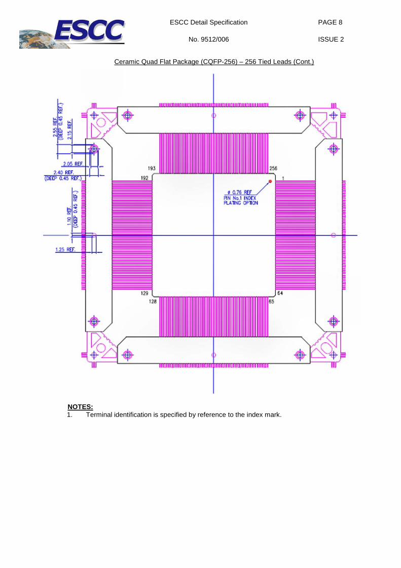
1.7 PHYSICAL DIMENSIONS AND TERMINAL IDENTIFICATION
Ceramic Quad Flat Package (CQFP-256) – 256 Tied Leads
ESCC Detail Specification
No. 9512/006
PAGE 8
ISSUE 2
Ceramic Quad Flat Package (CQFP-256) – 256 Tied Leads (Cont.)
NOTES: 1. Terminal identification is specified by reference to the index mark.
ESCC Detail Specification
No. 9512/006
PAGE 9
ISSUE 2
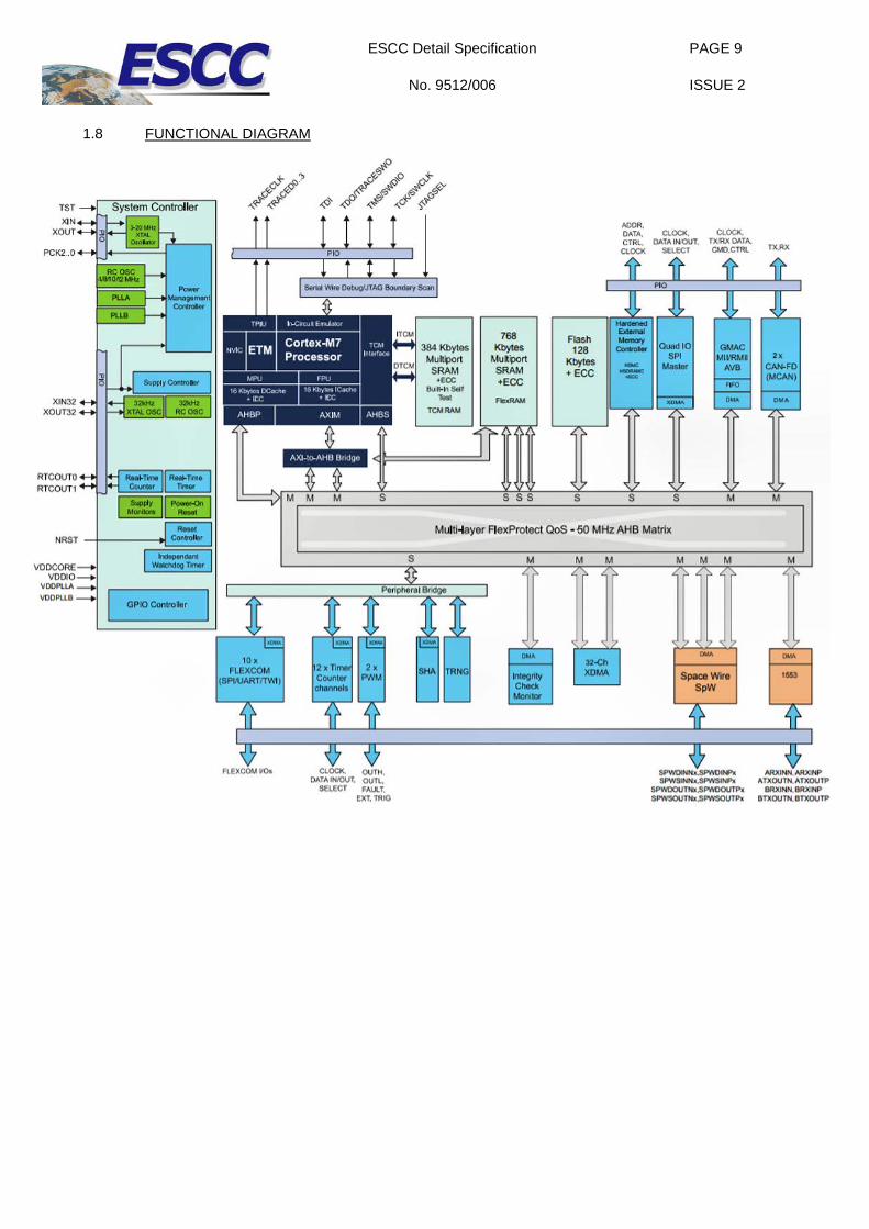
1.8 FUNCTIONAL DIAGRAM

ESCC Detail Specification
No. 9512/006
PAGE 10
ISSUE 2
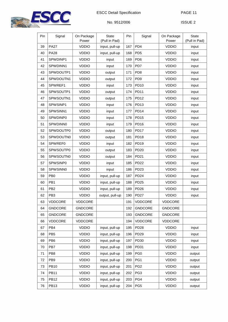
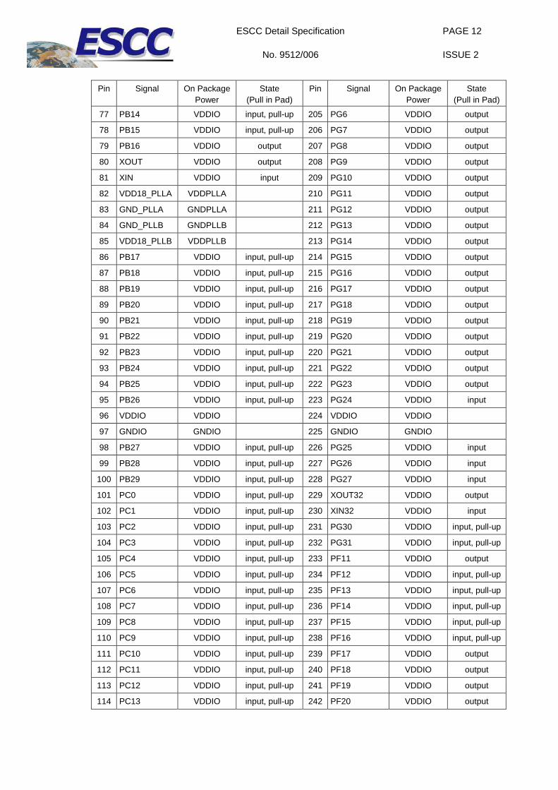
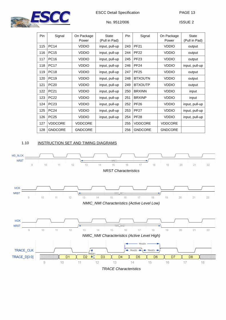
1.9 PIN ASSIGNMENT
Pin Signal On Package Power
State (Pull in Pad)
Pin Signal On Package Power
State (Pull in Pad)
1 GNDCORE GNDCORE GND 129 GNDCORE GNDCORE
2 VDDCORE VDDCORE PWR 130 VDDCORE VDDCORE
3 PF29 VDDIO input, pull-up 131 PC26 VDDIO input, pull-up
4 PF30 VDDIO input, pull-up 132 PC27 VDDIO input, pull-up
5 ATXOUTN VDDIO output 133 PC28 VDDIO input, pull-up
6 ATXOUTP VDDIO output 134 PC29 VDDIO input
7 ARXINN VDDIO input 135 PC30 VDDIO input
8 ARXINP VDDIO input 136 PC31 VDDIO input
9 PA0 VDDIO input, pull-up 137 PE12 VDDIO input
10 PA1 VDDIO input, pull-up 138 PE11 VDDIO input
11 PA2 VDDIO input, pull-up 139 PE10 VDDIO input
12 PA3 VDDIO input, pull-up 140 PE9 VDDIO input
13 PA4 VDDIO input, pull-up 141 PE8 VDDIO input
14 PA5 VDDIO input, pull-up 142 PE7 VDDIO input
15 PA6 VDDIO input, pull-up 143 PE6 VDDIO input
16 PA7 VDDIO input, pull-up 144 PE5 VDDIO input
17 PA8 VDDIO input, pull-up 145 PE4 VDDIO input
18 PA9 VDDIO input, pull-up 146 PE3 VDDIO input
19 PA10 VDDIO input, pull-up 147 PE2 VDDIO input
20 PA11 VDDIO input, pull-up 148 PE1 VDDIO input
21 PA12 VDDIO input, pull-up 149 PE0 VDDIO input
22 PA13 VDDIO output 150 PF0 VDDIO input, pull-up
23 TST VDDIO input, pull-down 151 PF1 VDDIO input, pull-up
24 JTAGSEL VDDIO input, pull-down 152 PF2 VDDIO input, pull-up
25 NMIC_NMI VDDIO input, pull-up 153 PF3 VDDIO input, pull-up
26 PA16 VDDIO input 154 PF4 VDDIO input, pull-up
27 PA17 VDDIO input 155 PF5 VDDIO input, pull-up
28 NRST VDDIO input, pull-up 156 PF6 VDDIO input, pull-up
29 PA19 VDDIO input, pull-up 157 PF7 VDDIO input, pull-up
30 PA20 VDDIO input, pull-up 158 PF8 VDDIO input, pull-up
31 PA21 VDDIO input, pull-up 159 PF9 VDDIO input, pull-up
32 VDDIO VDDIO 160 VDDIO VDDIO
33 GNDIO GNDIO 161 GNDIO GNDIO
34 PA22 VDDIO input, pull-up 162 PF10 VDDIO input, pull-up
35 PA23 VDDIO input, pull-up 163 PD0 VDDIO input
36 PA24 VDDIO input, pull-up 164 PD1 VDDIO input
37 PA25 VDDIO input, pull-up 165 PD2 VDDIO input
38 PA26 VDDIO input, pull-up 166 PD3 VDDIO input
ESCC Detail Specification
No. 9512/006
PAGE 11
ISSUE 2
Pin Signal On Package
Power State
(Pull in Pad) Pin Signal On Package
Power State
(Pull in Pad)
39 PA27 VDDIO input, pull-up 167 PD4 VDDIO input
40 PA28 VDDIO input, pull-up 168 PD5 VDDIO input
41 SPWDINP1 VDDIO input 169 PD6 VDDIO input
42 SPWDINN1 VDDIO input 170 PD7 VDDIO input
43 SPWDOUTP1 VDDIO output 171 PD8 VDDIO input
44 SPWDOUTN1 VDDIO output 172 PD9 VDDIO input
45 SPWREF1 VDDIO input 173 PD10 VDDIO input
46 SPWSOUTP1 VDDIO output 174 PD11 VDDIO input
47 SPWSOUTN1 VDDIO output 175 PD12 VDDIO input
48 SPWSINP1 VDDIO input 176 PD13 VDDIO input
49 SPWSINN1 VDDIO input 177 PD14 VDDIO input
50 SPWDINP0 VDDIO input 178 PD15 VDDIO input
51 SPWDINN0 VDDIO input 179 PD16 VDDIO input
52 SPWDOUTP0 VDDIO output 180 PD17 VDDIO input
53 SPWDOUTN0 VDDIO output 181 PD18 VDDIO input
54 SPWREF0 VDDIO input 182 PD19 VDDIO input
55 SPWSOUTP0 VDDIO output 183 PD20 VDDIO input
56 SPWSOUTN0 VDDIO output 184 PD21 VDDIO input
57 SPWSINP0 VDDIO input 185 PD22 VDDIO input
58 SPWSINN0 VDDIO input 186 PD23 VDDIO input
59 PB0 VDDIO input, pull-up 187 PD24 VDDIO input
60 PB1 VDDIO input, pull-up 188 PD25 VDDIO input
61 PB2 VDDIO input, pull-up 189 PD26 VDDIO input
62 PB3 VDDIO output, pull-up 190 PD27 VDDIO input
63 VDDCORE VDDCORE 191 VDDCORE VDDCORE
64 GNDCORE GNDCORE 192 GNDCORE GNDCORE
65 GNDCORE GNDCORE 193 GNDCORE GNDCORE
66 VDDCORE VDDCORE 194 VDDCORE VDDCORE
67 PB4 VDDIO input, pull-up 195 PD28 VDDIO input
68 PB5 VDDIO input, pull-up 196 PD29 VDDIO input
69 PB6 VDDIO input, pull-up 197 PD30 VDDIO input
70 PB7 VDDIO input, pull-up 198 PD31 VDDIO input
71 PB8 VDDIO input, pull-up 199 PG0 VDDIO output
72 PB9 VDDIO input, pull-up 200 PG1 VDDIO output
73 PB10 VDDIO input, pull-up 201 PG2 VDDIO output
74 PB11 VDDIO input, pull-up 202 PG3 VDDIO output
75 PB12 VDDIO input, pull-up 203 PG4 VDDIO output
76 PB13 VDDIO input, pull-up 204 PG5 VDDIO output
ESCC Detail Specification
No. 9512/006
PAGE 12
ISSUE 2
Pin Signal On Package
Power State
(Pull in Pad) Pin Signal On Package
Power State
(Pull in Pad)
77 PB14 VDDIO input, pull-up 205 PG6 VDDIO output
78 PB15 VDDIO input, pull-up 206 PG7 VDDIO output
79 PB16 VDDIO output 207 PG8 VDDIO output
80 XOUT VDDIO output 208 PG9 VDDIO output
81 XIN VDDIO input 209 PG10 VDDIO output
82 VDD18_PLLA VDDPLLA 210 PG11 VDDIO output
83 GND_PLLA GNDPLLA 211 PG12 VDDIO output
84 GND_PLLB GNDPLLB 212 PG13 VDDIO output
85 VDD18_PLLB VDDPLLB 213 PG14 VDDIO output
86 PB17 VDDIO input, pull-up 214 PG15 VDDIO output
87 PB18 VDDIO input, pull-up 215 PG16 VDDIO output
88 PB19 VDDIO input, pull-up 216 PG17 VDDIO output
89 PB20 VDDIO input, pull-up 217 PG18 VDDIO output
90 PB21 VDDIO input, pull-up 218 PG19 VDDIO output
91 PB22 VDDIO input, pull-up 219 PG20 VDDIO output
92 PB23 VDDIO input, pull-up 220 PG21 VDDIO output
93 PB24 VDDIO input, pull-up 221 PG22 VDDIO output
94 PB25 VDDIO input, pull-up 222 PG23 VDDIO output
95 PB26 VDDIO input, pull-up 223 PG24 VDDIO input
96 VDDIO VDDIO 224 VDDIO VDDIO
97 GNDIO GNDIO 225 GNDIO GNDIO
98 PB27 VDDIO input, pull-up 226 PG25 VDDIO input
99 PB28 VDDIO input, pull-up 227 PG26 VDDIO input
100 PB29 VDDIO input, pull-up 228 PG27 VDDIO input
101 PC0 VDDIO input, pull-up 229 XOUT32 VDDIO output
102 PC1 VDDIO input, pull-up 230 XIN32 VDDIO input
103 PC2 VDDIO input, pull-up 231 PG30 VDDIO input, pull-up
104 PC3 VDDIO input, pull-up 232 PG31 VDDIO input, pull-up
105 PC4 VDDIO input, pull-up 233 PF11 VDDIO output
106 PC5 VDDIO input, pull-up 234 PF12 VDDIO input, pull-up
107 PC6 VDDIO input, pull-up 235 PF13 VDDIO input, pull-up
108 PC7 VDDIO input, pull-up 236 PF14 VDDIO input, pull-up
109 PC8 VDDIO input, pull-up 237 PF15 VDDIO input, pull-up
110 PC9 VDDIO input, pull-up 238 PF16 VDDIO input, pull-up
111 PC10 VDDIO input, pull-up 239 PF17 VDDIO output
112 PC11 VDDIO input, pull-up 240 PF18 VDDIO output
113 PC12 VDDIO input, pull-up 241 PF19 VDDIO output
114 PC13 VDDIO input, pull-up 242 PF20 VDDIO output
ESCC Detail Specification
No. 9512/006
PAGE 13
ISSUE 2
Pin Signal On Package
Power State
(Pull in Pad) Pin Signal On Package
Power State
(Pull in Pad)
115 PC14 VDDIO input, pull-up 243 PF21 VDDIO output
116 PC15 VDDIO input, pull-up 244 PF22 VDDIO output
117 PC16 VDDIO input, pull-up 245 PF23 VDDIO output
118 PC17 VDDIO input, pull-up 246 PF24 VDDIO input, pull-up
119 PC18 VDDIO input, pull-up 247 PF25 VDDIO output
120 PC19 VDDIO input, pull-up 248 BTXOUTN VDDIO output
121 PC20 VDDIO input, pull-up 249 BTXOUTP VDDIO output
122 PC21 VDDIO input, pull-up 250 BRXINN VDDIO input
123 PC22 VDDIO input, pull-up 251 BRXINP VDDIO input
124 PC23 VDDIO input, pull-up 252 PF26 VDDIO input, pull-up
125 PC24 VDDIO input, pull-up 253 PF27 VDDIO input, pull-up
126 PC25 VDDIO input, pull-up 254 PF28 VDDIO input, pull-up
127 VDDCORE VDDCORE 255 VDDCORE VDDCORE
128 GNDCORE GNDCORE 256 GNDCORE GNDCORE
1.10 INSTRUCTION SET AND TIMING DIAGRAMS
NRST Characteristics
NMIC_NMI Characteristics (Active Level Low)
NMIC_NMI Characteristics (Active Level High)
TRACE Characteristics
ESCC Detail Specification
No. 9512/006
PAGE 14
ISSUE 2
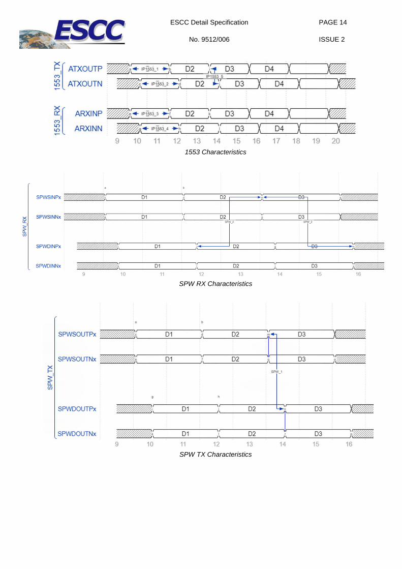
1553 Characteristics
SPW RX Characteristics
SPW TX Characteristics
ESCC Detail Specification
No. 9512/006
PAGE 15
ISSUE 2
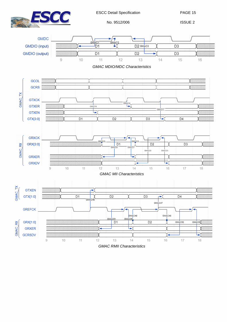
GMAC MDIO/MDC Characteristics
GMAC MII Characteristics
GMAC RMII Characteristics
ESCC Detail Specification
No. 9512/006
PAGE 16
ISSUE 2
QSPI Master Mode (CPOL=0 and NCPHA=0) or (CPOL=1 and NCPHA=1)
QSPI Master Mode (CPOL=0 and NCPHA=1) or (CPOL=1 and NCPHA=0)
FlexCOM SPI Characteristics Master Mode (CPOL=0 and NCPHA=0) or (CPOL=1 and NCPHA=1)
FlexCOM SPI Characteristics Master Mode (CPOL=0 and NCPHA=1) or (CPOL=1 and NCPHA=0)
FlexCOM SPI Characteristics Slave Mode (CPOL=0 and NCPHA=0) or (CPOL=1 and NCPHA=1)
ESCC Detail Specification
No. 9512/006
PAGE 17
ISSUE 2
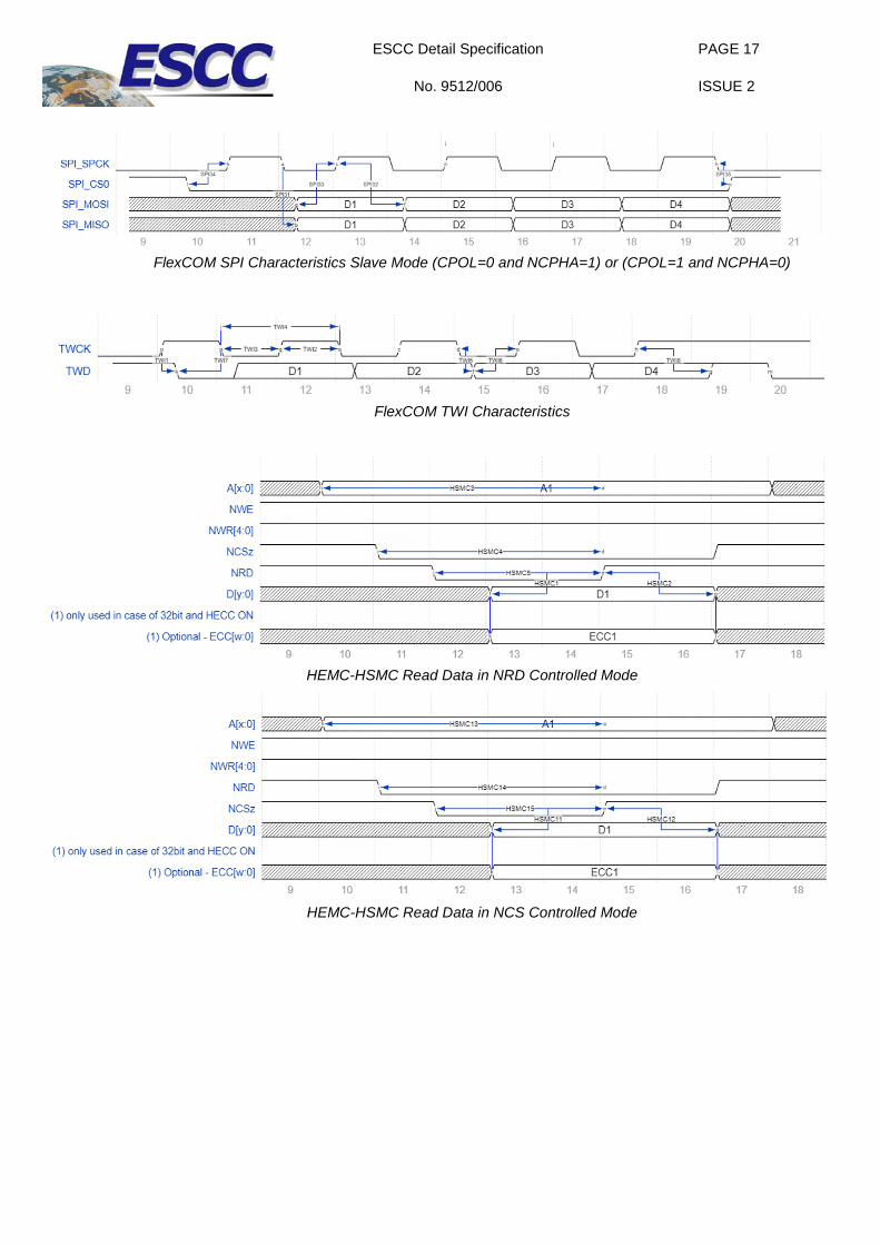
FlexCOM SPI Characteristics Slave Mode (CPOL=0 and NCPHA=1) or (CPOL=1 and NCPHA=0)
FlexCOM TWI Characteristics
HEMC-HSMC Read Data in NRD Controlled Mode
HEMC-HSMC Read Data in NCS Controlled Mode

ESCC Detail Specification
No. 9512/006
PAGE 18
ISSUE 2
HEMC-HSMC Write Data in NCS Controlled Mode
HEMC-HSMC Write Data in NWE Controlled Mode
HEMC HSDRAMC Read Word Access 32-bit Memory (HECC ON/OFF)
ESCC Detail Specification
No. 9512/006
PAGE 19
ISSUE 2
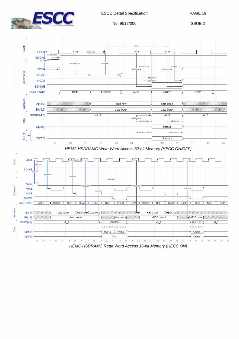
HEMC HSDRAMC Write Word Access 32-bit Memory (HECC ON/OFF)
HEMC HSDRAMC Read Word Access 16-bit Memory (HECC ON)
ESCC Detail Specification
No. 9512/006
PAGE 20
ISSUE 2
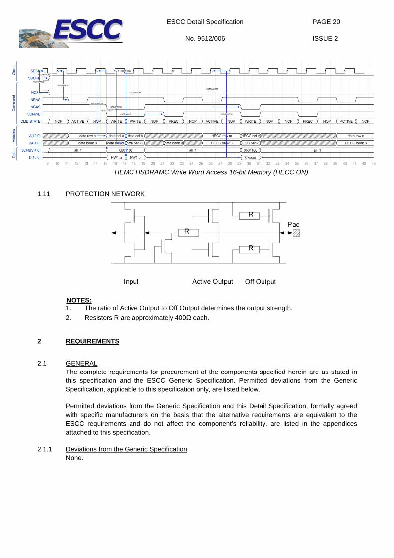
HEMC HSDRAMC Write Word Access 16-bit Memory (HECC ON)
1.11 PROTECTION NETWORK
NOTES: 1. The ratio of Active Output to Off Output determines the output strength. 2. Resistors R are approximately 400Ω each.
2 REQUIREMENTS
2.1 GENERAL The complete requirements for procurement of the components specified herein are as stated in this specification and the ESCC Generic Specification. Permitted deviations from the Generic Specification, applicable to this specification only, are listed below.
Permitted deviations from the Generic Specification and this Detail Specification, formally agreed with specific manufacturers on the basis that the alternative requirements are equivalent to the ESCC requirements and do not affect the component’s reliability, are listed in the appendices attached to this specification.
2.1.1 Deviations from the Generic Specification None.
ESCC Detail Specification
No. 9512/006
PAGE 21
ISSUE 2
2.2 MARKING
The marking shall be in accordance with the requirements of ESCC Basic Specification No. 21700 and as follows.
The information to be marked on the component shall be:
(a) Terminal identification (see Para. 1.7). (b) The ESCC qualified components symbol (for ESCC qualified component only). (c) The ESCC Component Number (see Para. 1.4.1). (d) Traceability information.
2.3 ELECTRICAL MEASUREMENTS AT ROOM, HIGH AND LOW TEMPERATURES Electrical measurements shall be performed at room, high and low temperatures.
2.3.1 Room Temperature Electrical Measurements The measurements shall be performed at Tcase = +25(+3 -5)°C.
Characteristics Symbols MIL-STD-883 Test Method
Test Conditions 1.65V < VDD < 1.95V
3V < VCC < 3.6V (Note 1)
Limits Units
Min Max
Functional Tests (Min.) - 3014 VDD = 1.65V VCC = 3V VIH = VDD VIL = VSS
- - -
Functional Tests (Typ.) - 3014 VDD = 1.8V VCC = 3.3V VIH = VDD VIL = VSS
- - -
Functional Tests (Max.) - 3014 VDD = 1.95V VCC = 3.6V VIH = VDD VIL = VSS
- - -
Low Level Input Voltage VIL - CMOS buffers (Note 2)
- 700 mV
High Level Input Voltage VIH - CMOS buffers (Note 2)
2 - V
Low Level Output Voltage
VOL 3007 CMOS buffers IOL= 2, 4, 8, 16, 24, 32, 40, 48mA
- 400 mV
High Level Output Voltage
VOH 3006 CMOS buffers IOH = -2, -4, -8, -16, -24, -32, -40, -48mA
VCC-0.4 - V
Low Level Input Current (General case, excepts pads: PA0/1/6/7/12/13/16/17)
IOZL 3009 CMOS buffers VIN = VSS
-1 1 µA
Low Level Input Current (Case of pads: PA0/1/6/7/12/13/16/17)
IOZL2 3009 CMOS buffers VIN = VSS
-3 3 µA
Low Level Input Current with Pull-down
IOZLPD 3009 CMOS buffers VIN = VSS
-3 3 µA
ESCC Detail Specification
No. 9512/006
PAGE 22
ISSUE 2
Characteristics Symbols MIL-STD-883
Test Method Test Conditions
1.65V < VDD < 1.95V 3V < VCC < 3.6V
(Note 1)
Limits Units
Min Max
Low Level Input Current with Pull-up
IOZLPU 3009 CMOS buffers VIN = VSS
-480 -160 µA
High Level Input Current (General case, except pads: PA0/1/6/7/12/13/16/17)
IOZH 3010 CMOS buffers VIN = VCC max
-1 1 µA
High Level Input Current (Case of pads: PA0/1/6/7/12/13/16/17)
IOZH2 3010 CMOS buffers VIN = VCC max
-3 3 µA
High Level Input Current with Pull-up
IOZHPU 3010 CMOS buffers VIN = VCC max
-3 3 µA
High Level Input Current with Pull-down
IOZHPD 3010 CMOS buffers VIN = VCC max
237 723 µA
ColdSparing (General case, except pads: PA0/6/12/16)
CS 3010 CMOS buffers VIN = VCC max (Note 3)
-1 1 µA
ColdSparing (Case of pads: PA0/6/12/16)
CS2 3010 CMOS buffers VIN = VCC max (Note 3)
-5 5 µA
LVDS Differential Output Voltage
VODTX 3006 3007
247 454 mV
LVDS Difference of Magnitude of VOD for opposite binary state
DVODTX 3006 3007
- 50 mV
LVDS Offset Voltage VOSTX 3006 3007
1.125 1.375 V
LVDS Difference of Magnitude of VOS for opposite binary state
DVOSTX 3006 3007
- 50 mV
Array Stand-by Current ICCSBA 3005 VDD max Output = 0mA (Note 4)
- 50 mA
Array Operating Current ICCOP 3005 VDD max VCC max Processor clock = 100MHz System clock = 50MHz
- 1.9 A
Input Pin Capacitance CI33 3012 CMOS buffers (Note 5)
- 7 pF
Operating Period RC 32kHz
tOSC 3003 (Note 6) 25 41.6 µs
Operating Period after calibration RC 4MHz
tACC4 3003 (Note 6) 227.3 277.7 ns
Operating Period after calibration RC 8MHz
tACC8 3003 (Note 6) 113.7 138.9 ns
Operating Period after calibration RC 10MHz
tACC10 3003 (Note 6) 90.9 111.1 ns
ESCC Detail Specification
No. 9512/006
PAGE 23
ISSUE 2
Characteristics Symbols MIL-STD-883
Test Method Test Conditions
1.65V < VDD < 1.95V 3V < VCC < 3.6V
(Note 1)
Limits Units
Min Max
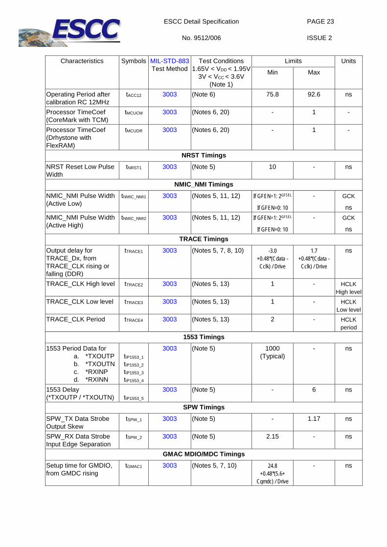
Operating Period after calibration RC 12MHz
tACC12 3003 (Note 6) 75.8 92.6 ns
Processor TimeCoef (CoreMark with TCM)
tMCUCM 3003 (Notes 6, 20) - 1 -
Processor TimeCoef (Drhystone with FlexRAM)
tMCUDR 3003 (Notes 6, 20) - 1 -
NRST Timings
NRST Reset Low Pulse Width
tNRST1 3003 (Note 5) 10 - ns
NMIC_NMI Timings
NMIC_NMI Pulse Width (Active Low)
tNMIC_NMI1 3003 (Notes 5, 11, 12) If GFEN=1: 2GFSEL
If GFEN=0: 10
- GCK
ns NMIC_NMI Pulse Width (Active High)
tNMIC_NMI2 3003 (Notes 5, 11, 12) If GFEN=1: 2GFSEL
If GFEN=0: 10
- GCK
ns TRACE Timings
Output delay for TRACE_Dx, from TRACE_CLK rising or falling (DDR)
tTRACE1 3003 (Notes 5, 7, 8, 10) -3.0 +0.48*(Cdata -Cclk) / Drive
1.7 +0.48*(Cdata - Cclk) / Drive
ns
TRACE_CLK High level tTRACE2 3003 (Notes 5, 13) 1 - HCLK High level
TRACE_CLK Low level tTRACE3 3003 (Notes 5, 13) 1 - HCLK Low level
TRACE_CLK Period tTRACE4 3003 (Notes 5, 13) 2 - HCLK period
1553 Timings 1553 Period Data for
a. *TXOUTP b. *TXOUTN c. *RXINP d. *RXINN
tIP1553_1 tIP1553_2 tIP1553_3 tIP1553_4
3003 (Note 5) 1000 (Typical)
- ns
1553 Delay (*TXOUTP / *TXOUTN)
tIP1553_5
3003 (Note 5) - 6 ns
SPW Timings SPW_TX Data Strobe Output Skew
tSPW_1 3003 (Note 5) - 1.17 ns
SPW_RX Data Strobe Input Edge Separation
tSPW_2 3003 (Note 5) 2.15 - ns
GMAC MDIO/MDC Timings Setup time for GMDIO, from GMDC rising
tGMAC1 3003 (Notes 5, 7, 10) 24.8 +0.48*(5.6+
Cgmdc) / Drive
- ns
ESCC Detail Specification
No. 9512/006
PAGE 24
ISSUE 2
Characteristics Symbols MIL-STD-883
Test Method Test Conditions
1.65V < VDD < 1.95V 3V < VCC < 3.6V
(Note 1)
Limits Units
Min Max
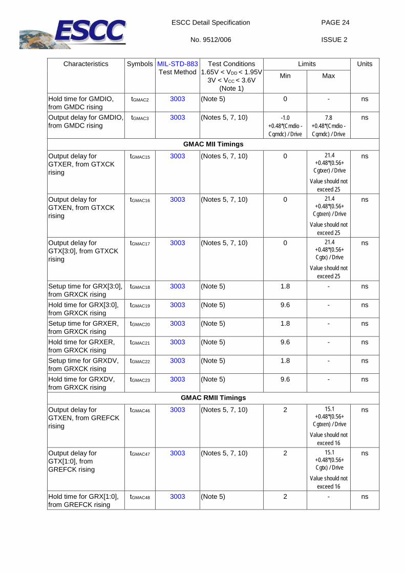
Hold time for GMDIO, from GMDC rising
tGMAC2 3003 (Note 5) 0 - ns
Output delay for GMDIO, from GMDC rising
tGMAC3 3003 (Notes 5, 7, 10) -1.0 +0.48*(Cmdio - Cgmdc) / Drive
7.8 +0.48*(Cmdio -Cgmdc) / Drive
ns
GMAC MII Timings Output delay for GTXER, from GTXCK rising
tGMAC15 3003 (Notes 5, 7, 10) 0 21.4 +0.48*(0.56+
Cgtxer) / Drive
Value should not exceed 25
ns
Output delay for GTXEN, from GTXCK rising
tGMAC16 3003 (Notes 5, 7, 10) 0 21.4 +0.48*(0.56+
Cgtxen) / Drive
Value should not exceed 25
ns
Output delay for GTX[3:0], from GTXCK rising
tGMAC17 3003 (Notes 5, 7, 10) 0 21.4 +0.48*(0.56+ Cgtx) / Drive
Value should not exceed 25
ns
Setup time for GRX[3:0], from GRXCK rising
tGMAC18 3003 (Note 5) 1.8 - ns
Hold time for GRX[3:0], from GRXCK rising
tGMAC19 3003 (Note 5) 9.6 - ns
Setup time for GRXER, from GRXCK rising
tGMAC20 3003 (Note 5) 1.8 - ns
Hold time for GRXER, from GRXCK rising
tGMAC21 3003 (Note 5) 9.6 - ns
Setup time for GRXDV, from GRXCK rising
tGMAC22 3003 (Note 5) 1.8 - ns
Hold time for GRXDV, from GRXCK rising
tGMAC23 3003 (Note 5) 9.6 - ns
GMAC RMII Timings Output delay for GTXEN, from GREFCK rising
tGMAC46 3003 (Notes 5, 7, 10) 2 15.1 +0.48*(0.56+
Cgtxen) / Drive
Value should not exceed 16
ns
Output delay for GTX[1:0], from GREFCK rising
tGMAC47 3003 (Notes 5, 7, 10) 2 15.1 +0.48*(0.56+ Cgtx) / Drive
Value should not exceed 16
ns
Hold time for GRX[1:0], from GREFCK rising
tGMAC48 3003 (Note 5) 2 - ns
ESCC Detail Specification
No. 9512/006
PAGE 25
ISSUE 2
Characteristics Symbols MIL-STD-883
Test Method Test Conditions
1.65V < VDD < 1.95V 3V < VCC < 3.6V
(Note 1)
Limits Units
Min Max
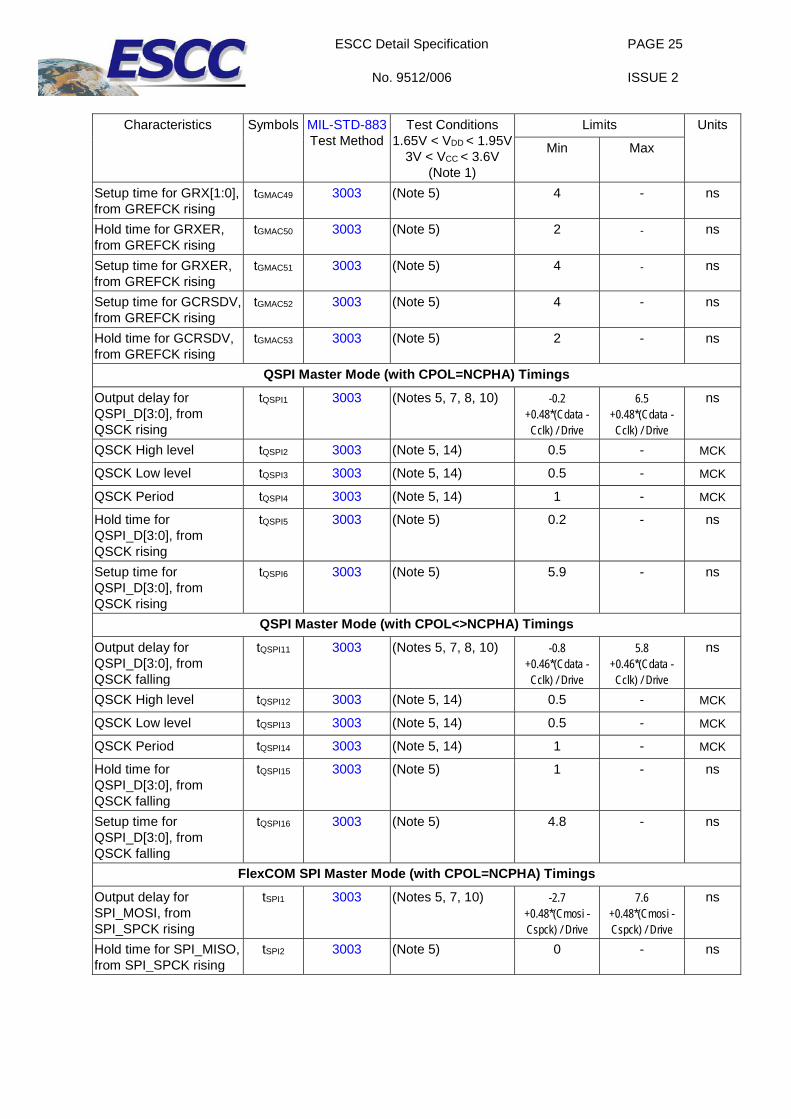
Setup time for GRX[1:0], from GREFCK rising
tGMAC49 3003 (Note 5) 4 - ns
Hold time for GRXER, from GREFCK rising
tGMAC50 3003 (Note 5) 2 - ns
Setup time for GRXER, from GREFCK rising
tGMAC51 3003 (Note 5) 4 - ns
Setup time for GCRSDV, from GREFCK rising
tGMAC52 3003 (Note 5) 4 - ns
Hold time for GCRSDV, from GREFCK rising
tGMAC53 3003 (Note 5) 2 - ns
QSPI Master Mode (with CPOL=NCPHA) Timings Output delay for QSPI_D[3:0], from QSCK rising
tQSPI1 3003 (Notes 5, 7, 8, 10) -0.2 +0.48*(Cdata - Cclk) / Drive
6.5 +0.48*(Cdata - Cclk) / Drive
ns
QSCK High level tQSPI2 3003 (Note 5, 14) 0.5 - MCK
QSCK Low level tQSPI3 3003 (Note 5, 14) 0.5 - MCK
QSCK Period tQSPI4 3003 (Note 5, 14) 1 - MCK
Hold time for QSPI_D[3:0], from QSCK rising
tQSPI5 3003 (Note 5) 0.2 - ns
Setup time for QSPI_D[3:0], from QSCK rising
tQSPI6 3003 (Note 5) 5.9 - ns
QSPI Master Mode (with CPOL<>NCPHA) Timings Output delay for QSPI_D[3:0], from QSCK falling
tQSPI11 3003 (Notes 5, 7, 8, 10) -0.8 +0.46*(Cdata - Cclk) / Drive
5.8 +0.46*(Cdata - Cclk) / Drive
ns
QSCK High level tQSPI12 3003 (Note 5, 14) 0.5 - MCK
QSCK Low level tQSPI13 3003 (Note 5, 14) 0.5 - MCK
QSCK Period tQSPI14 3003 (Note 5, 14) 1 - MCK
Hold time for QSPI_D[3:0], from QSCK falling
tQSPI15 3003 (Note 5) 1 - ns
Setup time for QSPI_D[3:0], from QSCK falling
tQSPI16 3003 (Note 5) 4.8 - ns
FlexCOM SPI Master Mode (with CPOL=NCPHA) Timings Output delay for SPI_MOSI, from SPI_SPCK rising
tSPI1 3003 (Notes 5, 7, 10) -2.7 +0.48*(Cmosi - Cspck) / Drive
7.6 +0.48*(Cmosi - Cspck) / Drive
ns
Hold time for SPI_MISO, from SPI_SPCK rising
tSPI2 3003 (Note 5) 0 - ns
ESCC Detail Specification
No. 9512/006
PAGE 26
ISSUE 2
Characteristics Symbols MIL-STD-883
Test Method Test Conditions
1.65V < VDD < 1.95V 3V < VCC < 3.6V
(Note 1)
Limits Units
Min Max
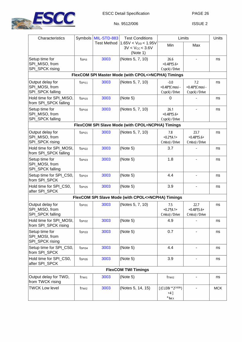
Setup time for SPI_MISO, from SPI_SPCK rising
tSPI3 3003 (Notes 5, 7, 10) 26.6 +0.48*(5.6+
Cspck) / Drive
- ns
FlexCOM SPI Master Mode (with CPOL<>NCPHA) Timings Output delay for SPI_MOSI, from SPI_SPCK falling
tSPI11 3003 (Notes 5, 7, 10) -3.0 +0.48*(Cmosi - Cspck) / Drive
7.2 +0.48*(Cmosi - Cspck) / Drive
ns
Hold time for SPI_MISO, from SPI_SPCK falling
tSPI15 3003 (Note 5) 0 - ns
Setup time for SPI_MISO, from SPI_SPCK falling
tSPI16 3003 (Notes 5, 7, 10) 26.1 +0.48*(5.6+
Cspck) / Drive
- ns
FlexCOM SPI Slave Mode (with CPOL=NCPHA) Timings Output delay for SPI_MISO, from SPI_SPCK rising
tSPI21 3003 (Notes 5, 7, 10) 7.8 +0.2*(4.1+
Cmiso) / Drive
23.7 +0.48*(5.6+
Cmiso) / Drive
ns
Hold time for SPI_MOSI, from SPI_SPCK falling
tSPI22 3003 (Note 5) 3.7 - ns
Setup time for SPI_MOSI, from SPI_SPCK falling
tSPI23 3003 (Note 5) 1.8 - ns
Setup time for SPI_CS0, from SPI_SPCK
tSPI24 3003 (Note 5) 4.4 - ns
Hold time for SPI_CS0, after SPI_SPCK
tSPI25 3003 (Note 5) 3.9 - ns
FlexCOM SPI Slave Mode (with CPOL<>NCPHA) Timings Output delay for SPI_MISO, from SPI_SPCK falling
tSPI31 3003 (Notes 5, 7, 10) 7.5 +0.2*(4.1+
Cmiso) / Drive
22.7 +0.48*(5.6+
Cmiso) / Drive
ns
Hold time for SPI_MOSI, from SPI_SPCK rising
tSPI32 3003 (Note 5) 4.9 - ns
Setup time for SPI_MOSI, from SPI_SPCK rising
tSPI33 3003 (Note 5) 0.7 - ns
Setup time for SPI_CS0, from SPI_SPCK
tSPI34 3003 (Note 5) 4.4 - ns
Hold time for SPI_CS0, after SPI_SPCK
tSPI35 3003 (Note 5) 3.9 - ns
FlexCOM TWI Timings Output delay for TWD, from TWCK rising
tTWI1 3003 (Note 5) tTWI2 - ns
TWCK Low level tTWI2 3003 (Notes 5, 14, 15) [ (CLDIV * 2CKDIV) +4 ]
* tMCK
- MCK

ESCC Detail Specification
No. 9512/006
PAGE 27
ISSUE 2
Characteristics Symbols MIL-STD-883
Test Method Test Conditions
1.65V < VDD < 1.95V 3V < VCC < 3.6V
(Note 1)
Limits Units
Min Max
TWCK High level tTWI3 3003 (Notes 5, 14, 15) [ (CHDIV * 2CKDIV) +4 ]
* tMCK
- MCK
TWCK Period tTWI4 3003 (Notes 5, 14, 15) [ [ (CLDIV + CHDIV) * 2CKDIV]
+8 ] * tMCK
- MCK
Hold time for TWD, from TWCK rising
tTWI5 3003 (Notes 5, 14) 0 3*tMCK ns
Setup time for TWD, from TWCK rising
tTWI6 3003 (Notes 5, 14) tTWI2 - 3*tMCK - ns
Output delay for TWD, from TWCK rising
tTWI7 3003 (Note 5) tTWI3 - ns
Output delay for TWD, from TWCK rising
tTWI8 3003 (Note 5) tTWI3 - ns
HEMC HSMC Timings: Read Data in NRD-Controlled Mode Setup time for D[y:0] and ECC[w:0], before NRD rising
tHSMC1 3003 (Notes 5, 7, 10) Hold = 19.0 +0.48*(5.6+ Cnrd) / Drive
No Hold = 29.0 +0.48*(5.6+ Cnrd) / Drive
- ns
Hold time for D[y:0] and ECC[w:0], after NRD rising
tHSMC2 3003 (Note 5) 0 - ns
A[x:0] valid, before NRD rising
tHSMC3 3003 (Notes 5, 7, 10, 14, 16)
(NRD_SETUP +NRD_PULSE) * tMCK - 12.3 -0.48*(Cnrd-
CA[x:0]) / Drive
- ns
NCSz valid, before NRD rising
tHSMC4 3003 (Notes 5, 7, 10, 14, 16)
(NRD_SETUP +NRD_PULSE
-NCS_RD_SETUP) * tMCK - 2.5
-0.48*(Cnrd-Cncs) / Drive
- ns
NRD Pulse Width tHSMC5 3003 (Notes 5, 14, 16) NRD_PULSE * tMCK - 3.0
- ns
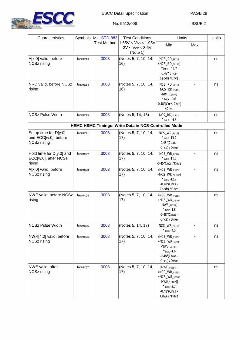
HEMC HSMC Timings: Read Data in NCS-Controlled Mode Setup time for D[y:0] and ECC[w:0], before NCSz rising
tHSMC11 3003 (Notes 5, 7, 10) Hold = 20.0 +0.48*(5.6+Cncs) /
Drive
No Hold = 30.0 +0.48*(5.6+ Cncs) / Drive
- ns
Hold time for D[y:0] and ECC[w:0], after NCSz rising
tHSMC12 3003 (Note 5) 0 - ns
ESCC Detail Specification
No. 9512/006
PAGE 28
ISSUE 2
Characteristics Symbols MIL-STD-883
Test Method Test Conditions
1.65V < VDD < 1.95V 3V < VCC < 3.6V
(Note 1)
Limits Units
Min Max
A[x:0] valid, before NCSz rising
tHSMC13 3003 (Notes 5, 7, 10, 14, 16)
(NCS_RD_SETUP +NCS_RD_PULSE)
* tMCK - 12.7 -0.48*(Cncs-
Caddr) / Drive
- ns
NRD valid, before NCSz rising
tHSMC14 3003 (Notes 5, 7, 10, 14, 16)
(NCS_RD_SETUP +NCS_RD_PULSE
-NRD_SETUP) * tMCK - 0.6
-0.48*(Cncs-Cnrd) / Drive
- ns
NCSz Pulse Width tHSMC15 3003 (Notes 5, 14, 16) NCS_RD_PULSE * tMCK – 4.5
- ns
HEMC HSMC Timings: Write Data in NCS-Controlled Mode Setup time for D[y:0] and ECC[w:0], before NCSz rising
tHSMC21 3003 (Notes 5, 7, 10, 14, 17)
NCS_WR_PULSE * tMCK -13.2
-0.48*(Cdata - Cncs) / Drive
- ns
Hold time for D[y:0] and ECC[w:0], after NCSz rising
tHSMC22 3003 (Notes 5, 7, 10, 14, 17)
NCS_WR_HOLD * tMCK -11.0
-0.45*Cncs / Drive
- ns
A[x:0] valid, before NCSz rising
tHSMC23 3003 (Notes 5, 7, 10, 14, 17)
(NCS_WR_PULSE +NCS_WR_SETUP)
* tMCK -12.7 -0.48*(Cncs - Caddr) / Drive
- ns
NWE valid, before NCSz rising
tHSMC24 3003 (Notes 5, 7, 10, 14, 17)
(NCS_WR_PULSE +NCS_WR_SETUP
-NWE_SETUP) * tMCK -1.6
-0.48*(Cnwe - Cncs) / Drive
- ns
NCSz Pulse Width tHSMC25 3003 (Notes 5, 14, 17) NCS_WR_PULSE * tMCK -4.5
- ns
NWR[4:0] valid, before NCSz rising
tHSMC26 3003 (Notes 5, 7, 10, 14, 17)
(NCS_WR_PULSE +NCS_WR_SETUP
-NWE_SETUP) * tMCK -1.6
-0.48*(Cnwe - Cncs) / Drive
- ns
NWE valid, after NCSz rising
tHSMC27 3003 (Notes 5, 7, 10, 14, 17)
[NWE_PULSE - (NCS_WR_PULSE +NCS_WR_SETUP
-NWE_SETUP)] * tMCK -2.7
-0.48*(Cncs - Cnwe) / Drive
- ns
ESCC Detail Specification
No. 9512/006
PAGE 29
ISSUE 2
Characteristics Symbols MIL-STD-883
Test Method Test Conditions
1.65V < VDD < 1.95V 3V < VCC < 3.6V
(Note 1)
Limits Units
Min Max
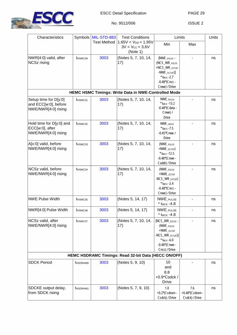
NWR[4:0] valid, after NCSz rising
tHSMC28 3003 (Notes 5, 7, 10, 14, 17)
[NWE_PULSE - (NCS_WR_PULSE +NCS_WR_SETUP
-NWE_SETUP)] * tMCK -2.7
-0.48*(Cncs - Cnwe) / Drive
- ns
HEMC HSMC Timings: Write Data in NWE-Controlled Mode Setup time for D[y:0] and ECC[w:0], before NWE/NWR[4:0] rising
tHSMC31 3003 (Notes 5, 7, 10, 14, 17)
NWE_PULSE * tMCK -13.2
-0.48*(Cdata - Cnwe) / Drive
- ns
Hold time for D[y:0] and ECC[w:0], after NWE/NWR[4:0] rising
tHSMC32 3003 (Notes 5, 7, 10, 14, 17)
NWE_HOLD * tMCK -7.5
-0.45*Cnwe / Drive
- ns
A[x:0] valid, before NWE/NWR[4:0] rising
tHSMC33 3003 (Notes 5, 7, 10, 14, 17)
(NWE_PULSE +NWE_SETUP) * tMCK -12.5
-0.48*(Cnwe - Caddr) / Drive
- ns
NCSz valid, before NWE/NWR[4:0] rising
tHSMC34 3003 (Notes 5, 7, 10, 14, 17)
(NWE_PULSE +NWE_SETUP
-NCS_WR_SETUP) * tMCK -2.4
-0.48*(Cncs - Cnwe) / Drive
- ns
NWE Pulse Width tHSMC35 3003 (Notes 5, 14, 17) NWE_PULSE * tMCK -4.8
- ns
NWR[4:0] Pulse Width tHSMC36 3003 (Notes 5, 14, 17) NWE_PULSE * tMCK -4.8
- ns
NCSz valid, after NWE/NWR[4:0] rising
tHSMC37 3003 (Notes 5, 7, 10, 14, 17)
[NCS_WR_PULSE - (NWE_PULSE +NWE_SETUP
-NCS_WR_SETUP)] * tMCK -6.0
-0.48*(Cnwe - Cncs) / Drive
- ns
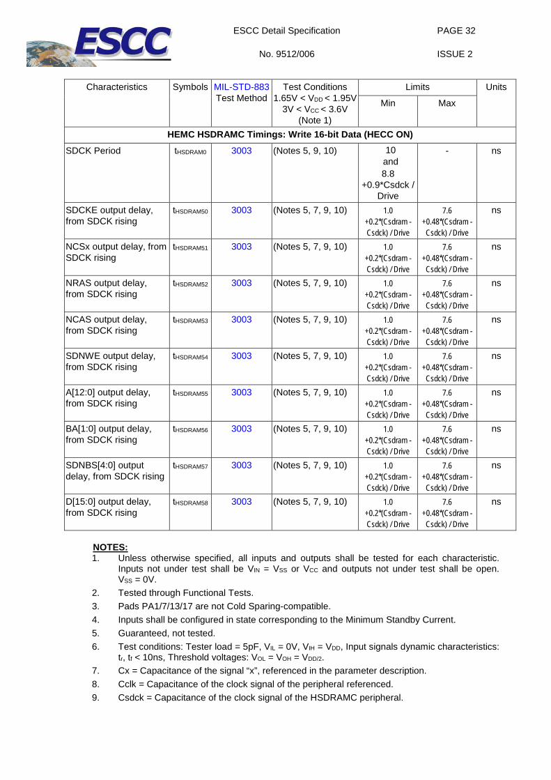
HEMC HSDRAMC Timings: Read 32-bit Data (HECC ON/OFF) SDCK Period tHSDRAM0 3003 (Notes 5, 9, 10) 10
and 8.8
+0.9*Csdck / Drive
- ns
SDCKE output delay, from SDCK rising
tHSDRAM1 3003 (Notes 5, 7, 9, 10) 1.0 +0.2*(Csdram - Csdck) / Drive
7.6 +0.48*(Csdram - Csdck) / Drive
ns
ESCC Detail Specification
No. 9512/006
PAGE 30
ISSUE 2
Characteristics Symbols MIL-STD-883
Test Method Test Conditions
1.65V < VDD < 1.95V 3V < VCC < 3.6V
(Note 1)
Limits Units
Min Max
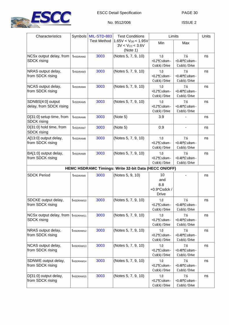
NCSx output delay, from SDCK rising
tHSDRAM2 3003 (Notes 5, 7, 9, 10) 1.0 +0.2*(Csdram - Csdck) / Drive
7.6 +0.48*(Csdram - Csdck) / Drive
ns
NRAS output delay, from SDCK rising
tHSDRAM3 3003 (Notes 5, 7, 9, 10) 1.0 +0.2*(Csdram - Csdck) / Drive
7.6 +0.48*(Csdram - Csdck) / Drive
ns
NCAS output delay, from SDCK rising
tHSDRAM4 3003 (Notes 5, 7, 9, 10) 1.0 +0.2*(Csdram - Csdck) / Drive
7.6 +0.48*(Csdram - Csdck) / Drive
ns
SDNBS[4:0] output delay, from SDCK rising
tHSDRAM5 3003 (Notes 5, 7, 9, 10) 1.0 +0.2*(Csdram - Csdck) / Drive
7.6 +0.48*(Csdram - Csdck) / Drive
ns
D[31:0] setup time, from SDCK rising
tHSDRAM6 3003 (Note 5) 3.9 - ns
D[31:0] hold time, from SDCK rising
tHSDRAM7 3003 (Note 5) 0.9 - ns
A[13:0] output delay, from SDCK rising
tHSDRAM8 3003 (Notes 5, 7, 9, 10) 1.0 +0.2*(Csdram - Csdck) / Drive
7.6 +0.48*(Csdram - Csdck) / Drive
ns
BA[1:0] output delay, from SDCK rising
tHSDRAM9 3003 (Notes 5, 7, 9, 10) 1.0 +0.2*(Csdram - Csdck) / Drive
7.6 +0.48*(Csdram - Csdck) / Drive
ns
HEMC HSDRAMC Timings: Write 32-bit Data (HECC ON/OFF) SDCK Period tHSDRAM0 3003 (Notes 5, 9, 10) 10
and 8.8
+0.9*Csdck / Drive
- ns
SDCKE output delay, from SDCK rising
tHSDRAM10 3003 (Notes 5, 7, 9, 10) 1.0 +0.2*(Csdram - Csdck) / Drive
7.6 +0.48*(Csdram - Csdck) / Drive
ns
NCSx output delay, from SDCK rising
tHSDRAM11 3003 (Notes 5, 7, 9, 10) 1.0 +0.2*(Csdram - Csdck) / Drive
7.6 +0.48*(Csdram - Csdck) / Drive
ns
NRAS output delay, from SDCK rising
tHSDRAM12 3003 (Notes 5, 7, 9, 10) 1.0 +0.2*(Csdram - Csdck) / Drive
7.6 +0.48*(Csdram - Csdck) / Drive
ns
NCAS output delay, from SDCK rising
tHSDRAM13 3003 (Notes 5, 7, 9, 10) 1.0 +0.2*(Csdram - Csdck) / Drive
7.6 +0.48*(Csdram - Csdck) / Drive
ns
SDNWE output delay, from SDCK rising
tHSDRAM14 3003 (Notes 5, 7, 9, 10) 1.0 +0.2*(Csdram - Csdck) / Drive
7.6 +0.48*(Csdram - Csdck) / Drive
ns
D[31:0] output delay, from SDCK rising
tHSDRAM15 3003 (Notes 5, 7, 9, 10) 1.0 +0.2*(Csdram - Csdck) / Drive
7.6 +0.48*(Csdram - Csdck) / Drive
ns
ESCC Detail Specification
No. 9512/006
PAGE 31
ISSUE 2
Characteristics Symbols MIL-STD-883
Test Method Test Conditions
1.65V < VDD < 1.95V 3V < VCC < 3.6V
(Note 1)
Limits Units
Min Max
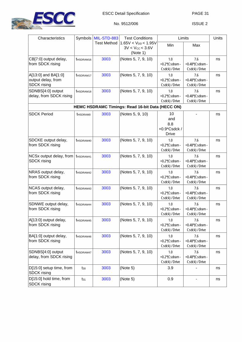
CB[7:0] output delay, from SDCK rising
tHSDRAM16 3003 (Notes 5, 7, 9, 10) 1.0 +0.2*(Csdram - Csdck) / Drive
7.6 +0.48*(Csdram - Csdck) / Drive
ns
A[13:0] and BA[1:0] output delay, from SDCK rising
tHSDRAM17 3003 (Notes 5, 7, 9, 10) 1.0 +0.2*(Csdram - Csdck) / Drive
7.6 +0.48*(Csdram - Csdck) / Drive
ns
SDNBS[4:0] output delay, from SDCK rising
tHSDRAM18 3003 (Notes 5, 7, 9, 10) 1.0 +0.2*(Csdram - Csdck) / Drive
7.6 +0.48*(Csdram - Csdck) / Drive
ns
HEMC HSDRAMC Timings: Read 16-bit Data (HECC ON) SDCK Period tHSDRAM0 3003 (Notes 5, 9, 10) 10
and 8.8
+0.9*Csdck / Drive
- ns
SDCKE output delay, from SDCK rising
tHSDRAM40 3003 (Notes 5, 7, 9, 10) 1.0 +0.2*(Csdram - Csdck) / Drive
7.6 +0.48*(Csdram - Csdck) / Drive
ns
NCSx output delay, from SDCK rising
tHSDRAM41 3003 (Notes 5, 7, 9, 10) 1.0 +0.2*(Csdram - Csdck) / Drive
7.6 +0.48*(Csdram - Csdck) / Drive
ns
NRAS output delay, from SDCK rising
tHSDRAM42 3003 (Notes 5, 7, 9, 10) 1.0 +0.2*(Csdram - Csdck) / Drive
7.6 +0.48*(Csdram - Csdck) / Drive
ns
NCAS output delay, from SDCK rising
tHSDRAM43 3003 (Notes 5, 7, 9, 10) 1.0 +0.2*(Csdram - Csdck) / Drive
7.6 +0.48*(Csdram - Csdck) / Drive
ns
SDNWE output delay, from SDCK rising
tHSDRAM44 3003 (Notes 5, 7, 9, 10) 1.0 +0.2*(Csdram - Csdck) / Drive
7.6 +0.48*(Csdram - Csdck) / Drive
ns
A[13:0] output delay, from SDCK rising
tHSDRAM45 3003 (Notes 5, 7, 9, 10) 1.0 +0.2*(Csdram - Csdck) / Drive
7.6 +0.48*(Csdram - Csdck) / Drive
ns
BA[1:0] output delay, from SDCK rising
tHSDRAM46 3003 (Notes 5, 7, 9, 10) 1.0 +0.2*(Csdram - Csdck) / Drive
7.6 +0.48*(Csdram - Csdck) / Drive
ns
SDNBS[4:0] output delay, from SDCK rising
tHSDRAM47 3003 (Notes 5, 7, 9, 10) 1.0 +0.2*(Csdram - Csdck) / Drive
7.6 +0.48*(Csdram - Csdck) / Drive
ns
D[15:0] setup time, from SDCK rising
t30 3003 (Note 5) 3.9 - ns
D[15:0] hold time, from SDCK rising
t31 3003 (Note 5) 0.9 - ns
ESCC Detail Specification
No. 9512/006
PAGE 32
ISSUE 2
Characteristics Symbols MIL-STD-883
Test Method Test Conditions
1.65V < VDD < 1.95V 3V < VCC < 3.6V
(Note 1)
Limits Units
Min Max
HEMC HSDRAMC Timings: Write 16-bit Data (HECC ON) SDCK Period tHSDRAM0 3003 (Notes 5, 9, 10) 10
and 8.8
+0.9*Csdck / Drive
- ns
SDCKE output delay, from SDCK rising
tHSDRAM50 3003 (Notes 5, 7, 9, 10) 1.0 +0.2*(Csdram - Csdck) / Drive
7.6 +0.48*(Csdram - Csdck) / Drive
ns
NCSx output delay, from SDCK rising
tHSDRAM51 3003 (Notes 5, 7, 9, 10) 1.0 +0.2*(Csdram - Csdck) / Drive
7.6 +0.48*(Csdram - Csdck) / Drive
ns
NRAS output delay, from SDCK rising
tHSDRAM52 3003 (Notes 5, 7, 9, 10) 1.0 +0.2*(Csdram - Csdck) / Drive
7.6 +0.48*(Csdram - Csdck) / Drive
ns
NCAS output delay, from SDCK rising
tHSDRAM53 3003 (Notes 5, 7, 9, 10) 1.0 +0.2*(Csdram - Csdck) / Drive
7.6 +0.48*(Csdram - Csdck) / Drive
ns
SDNWE output delay, from SDCK rising
tHSDRAM54 3003 (Notes 5, 7, 9, 10) 1.0 +0.2*(Csdram - Csdck) / Drive
7.6 +0.48*(Csdram - Csdck) / Drive
ns
A[12:0] output delay, from SDCK rising
tHSDRAM55 3003 (Notes 5, 7, 9, 10) 1.0 +0.2*(Csdram - Csdck) / Drive
7.6 +0.48*(Csdram - Csdck) / Drive
ns
BA[1:0] output delay, from SDCK rising
tHSDRAM56 3003 (Notes 5, 7, 9, 10) 1.0 +0.2*(Csdram - Csdck) / Drive
7.6 +0.48*(Csdram - Csdck) / Drive
ns
SDNBS[4:0] output delay, from SDCK rising
tHSDRAM57 3003 (Notes 5, 7, 9, 10) 1.0 +0.2*(Csdram - Csdck) / Drive
7.6 +0.48*(Csdram - Csdck) / Drive
ns
D[15:0] output delay, from SDCK rising
tHSDRAM58 3003 (Notes 5, 7, 9, 10) 1.0 +0.2*(Csdram - Csdck) / Drive
7.6 +0.48*(Csdram - Csdck) / Drive
ns
NOTES: 1. Unless otherwise specified, all inputs and outputs shall be tested for each characteristic.
Inputs not under test shall be VIN = VSS or VCC and outputs not under test shall be open. VSS = 0V.
2. Tested through Functional Tests. 3. Pads PA1/7/13/17 are not Cold Sparing-compatible. 4. Inputs shall be configured in state corresponding to the Minimum Standby Current. 5. Guaranteed, not tested. 6. Test conditions: Tester load = 5pF, VIL = 0V, VIH = VDD, Input signals dynamic characteristics:
tr, tf < 10ns, Threshold voltages: VOL = VOH = VDD/2. 7. Cx = Capacitance of the signal “x”, referenced in the parameter description. 8. Cclk = Capacitance of the clock signal of the peripheral referenced. 9. Csdck = Capacitance of the clock signal of the HSDRAMC peripheral.
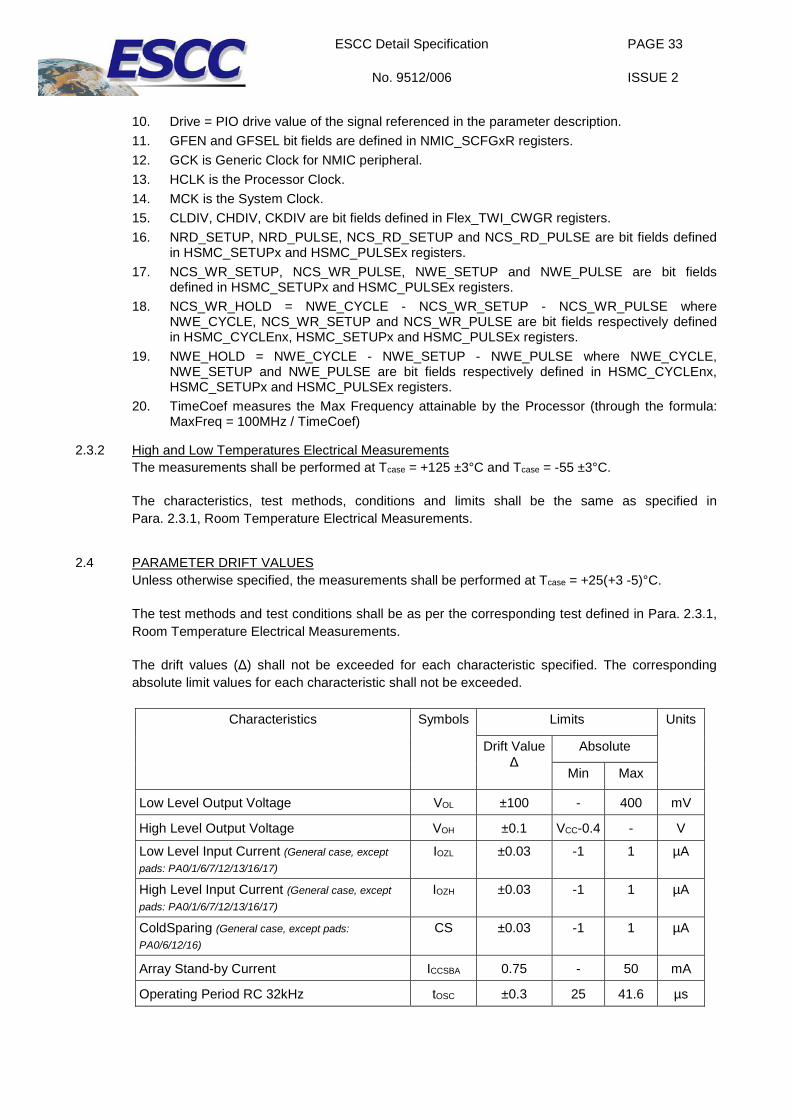
ESCC Detail Specification
No. 9512/006
PAGE 33
ISSUE 2
10. Drive = PIO drive value of the signal referenced in the parameter description. 11. GFEN and GFSEL bit fields are defined in NMIC_SCFGxR registers. 12. GCK is Generic Clock for NMIC peripheral. 13. HCLK is the Processor Clock. 14. MCK is the System Clock. 15. CLDIV, CHDIV, CKDIV are bit fields defined in Flex_TWI_CWGR registers. 16. NRD_SETUP, NRD_PULSE, NCS_RD_SETUP and NCS_RD_PULSE are bit fields defined
in HSMC_SETUPx and HSMC_PULSEx registers. 17. NCS_WR_SETUP, NCS_WR_PULSE, NWE_SETUP and NWE_PULSE are bit fields
defined in HSMC_SETUPx and HSMC_PULSEx registers. 18. NCS_WR_HOLD = NWE_CYCLE - NCS_WR_SETUP - NCS_WR_PULSE where
NWE_CYCLE, NCS_WR_SETUP and NCS_WR_PULSE are bit fields respectively defined in HSMC_CYCLEnx, HSMC_SETUPx and HSMC_PULSEx registers.
19. NWE_HOLD = NWE_CYCLE - NWE_SETUP - NWE_PULSE where NWE_CYCLE, NWE_SETUP and NWE_PULSE are bit fields respectively defined in HSMC_CYCLEnx, HSMC_SETUPx and HSMC_PULSEx registers.
20. TimeCoef measures the Max Frequency attainable by the Processor (through the formula: MaxFreq = 100MHz / TimeCoef)
2.3.2 High and Low Temperatures Electrical Measurements The measurements shall be performed at Tcase = +125 ±3°C and Tcase = -55 ±3°C.
The characteristics, test methods, conditions and limits shall be the same as specified in Para. 2.3.1, Room Temperature Electrical Measurements.
2.4 PARAMETER DRIFT VALUES Unless otherwise specified, the measurements shall be performed at Tcase = +25(+3 -5)°C.
The test methods and test conditions shall be as per the corresponding test defined in Para. 2.3.1, Room Temperature Electrical Measurements.
The drift values (Δ) shall not be exceeded for each characteristic specified. The corresponding absolute limit values for each characteristic shall not be exceeded.
Characteristics Symbols Limits Units
Drift Value Δ
Absolute
Min Max
Low Level Output Voltage VOL ±100 - 400 mV
High Level Output Voltage VOH ±0.1 VCC-0.4 - V
Low Level Input Current (General case, except pads: PA0/1/6/7/12/13/16/17)
IOZL ±0.03 -1 1 µA
High Level Input Current (General case, except pads: PA0/1/6/7/12/13/16/17)
IOZH ±0.03 -1 1 µA
ColdSparing (General case, except pads: PA0/6/12/16)
CS ±0.03 -1 1 µA
Array Stand-by Current ICCSBA 0.75 - 50 mA
Operating Period RC 32kHz tOSC ±0.3 25 41.6 µs
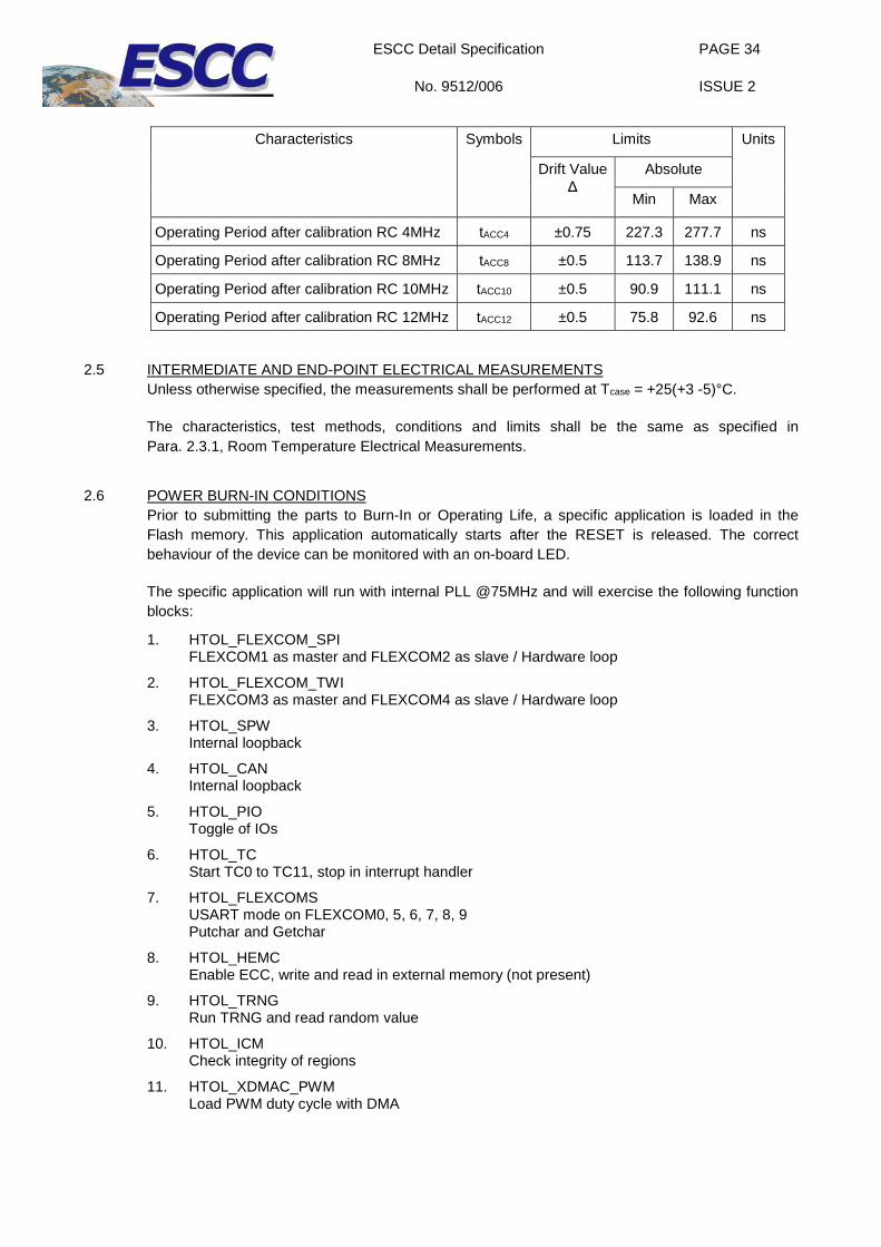
ESCC Detail Specification
No. 9512/006
PAGE 34
ISSUE 2
Characteristics Symbols Limits Units
Drift Value Δ
Absolute
Min Max
Operating Period after calibration RC 4MHz tACC4 ±0.75 227.3 277.7 ns
Operating Period after calibration RC 8MHz tACC8 ±0.5 113.7 138.9 ns
Operating Period after calibration RC 10MHz tACC10 ±0.5 90.9 111.1 ns
Operating Period after calibration RC 12MHz tACC12 ±0.5 75.8 92.6 ns
2.5 INTERMEDIATE AND END-POINT ELECTRICAL MEASUREMENTS Unless otherwise specified, the measurements shall be performed at Tcase = +25(+3 -5)°C.
The characteristics, test methods, conditions and limits shall be the same as specified in Para. 2.3.1, Room Temperature Electrical Measurements.
2.6 POWER BURN-IN CONDITIONS Prior to submitting the parts to Burn-In or Operating Life, a specific application is loaded in the Flash memory. This application automatically starts after the RESET is released. The correct behaviour of the device can be monitored with an on-board LED.
The specific application will run with internal PLL @75MHz and will exercise the following function blocks:
1. HTOL_FLEXCOM_SPI FLEXCOM1 as master and FLEXCOM2 as slave / Hardware loop
2. HTOL_FLEXCOM_TWI FLEXCOM3 as master and FLEXCOM4 as slave / Hardware loop
3. HTOL_SPW Internal loopback
4. HTOL_CAN Internal loopback
5. HTOL_PIO Toggle of IOs
6. HTOL_TC Start TC0 to TC11, stop in interrupt handler
7. HTOL_FLEXCOMS USART mode on FLEXCOM0, 5, 6, 7, 8, 9 Putchar and Getchar
8. HTOL_HEMC Enable ECC, write and read in external memory (not present)
9. HTOL_TRNG Run TRNG and read random value
10. HTOL_ICM Check integrity of regions
11. HTOL_XDMAC_PWM Load PWM duty cycle with DMA
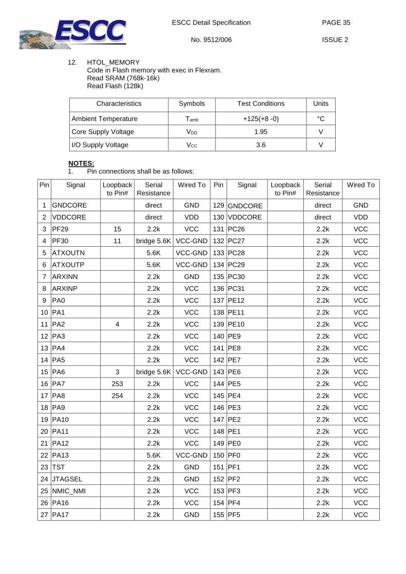
ESCC Detail Specification
No. 9512/006
PAGE 35
ISSUE 2
12. HTOL_MEMORY
Code in Flash memory with exec in Flexram. Read SRAM (768k-16k) Read Flash (128k)
Characteristics Symbols Test Conditions Units
Ambient Temperature Tamb +125(+8 -0) °C
Core Supply Voltage VDD 1.95 V
I/O Supply Voltage VCC 3.6 V
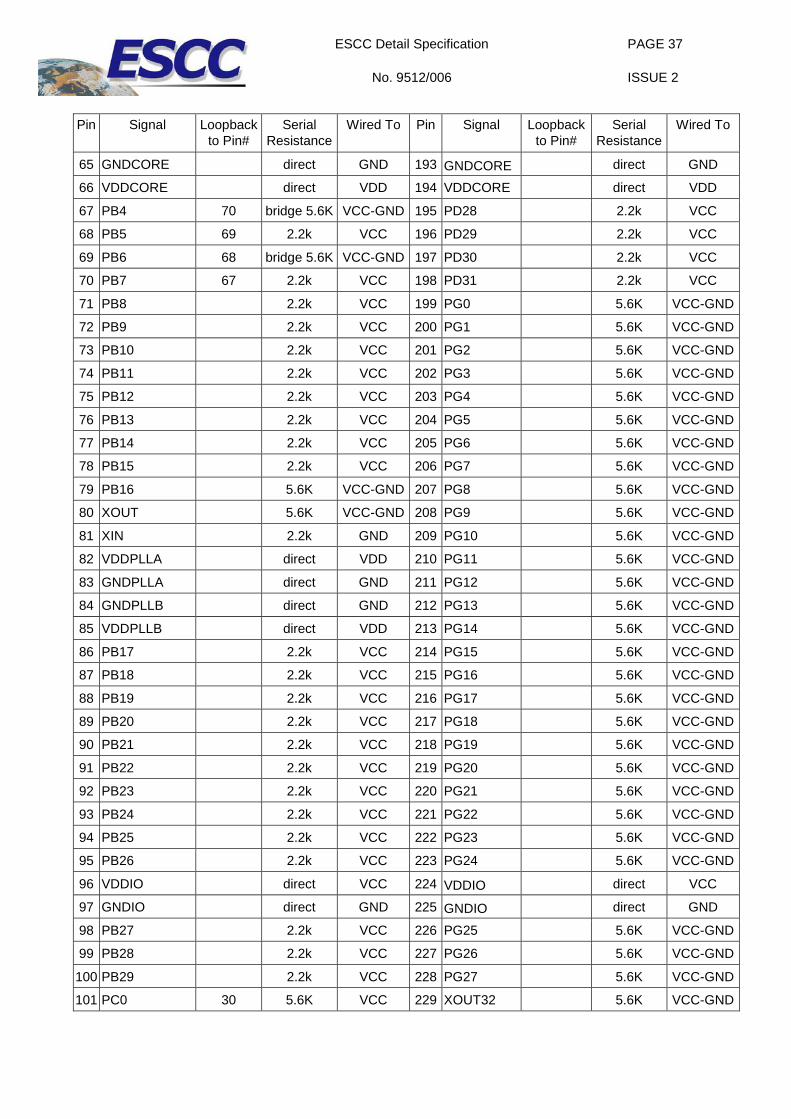
NOTES: 1. Pin connections shall be as follows:
Pin Signal Loopback to Pin#
Serial Resistance
Wired To Pin Signal Loopback to Pin#
Serial Resistance
Wired To
1 GNDCORE direct GND 129 GNDCORE direct GND
2 VDDCORE direct VDD 130 VDDCORE direct VDD
3 PF29 15 2.2k VCC 131 PC26 2.2k VCC
4 PF30 11 bridge 5.6K VCC-GND 132 PC27 2.2k VCC
5 ATXOUTN 5.6K VCC-GND 133 PC28 2.2k VCC
6 ATXOUTP 5.6K VCC-GND 134 PC29 2.2k VCC
7 ARXINN 2.2k GND 135 PC30 2.2k VCC
8 ARXINP 2.2k VCC 136 PC31 2.2k VCC
9 PA0 2.2k VCC 137 PE12 2.2k VCC
10 PA1 2.2k VCC 138 PE11 2.2k VCC
11 PA2 4 2.2k VCC 139 PE10 2.2k VCC
12 PA3 2.2k VCC 140 PE9 2.2k VCC
13 PA4 2.2k VCC 141 PE8 2.2k VCC
14 PA5 2.2k VCC 142 PE7 2.2k VCC
15 PA6 3 bridge 5.6K VCC-GND 143 PE6 2.2k VCC
16 PA7 253 2.2k VCC 144 PE5 2.2k VCC
17 PA8 254 2.2k VCC 145 PE4 2.2k VCC
18 PA9 2.2k VCC 146 PE3 2.2k VCC
19 PA10 2.2k VCC 147 PE2 2.2k VCC
20 PA11 2.2k VCC 148 PE1 2.2k VCC
21 PA12 2.2k VCC 149 PE0 2.2k VCC
22 PA13 5.6K VCC-GND 150 PF0 2.2k VCC
23 TST 2.2k GND 151 PF1 2.2k VCC
24 JTAGSEL 2.2k GND 152 PF2 2.2k VCC
25 NMIC_NMI 2.2k VCC 153 PF3 2.2k VCC
26 PA16 2.2k VCC 154 PF4 2.2k VCC
27 PA17 2.2k GND 155 PF5 2.2k VCC
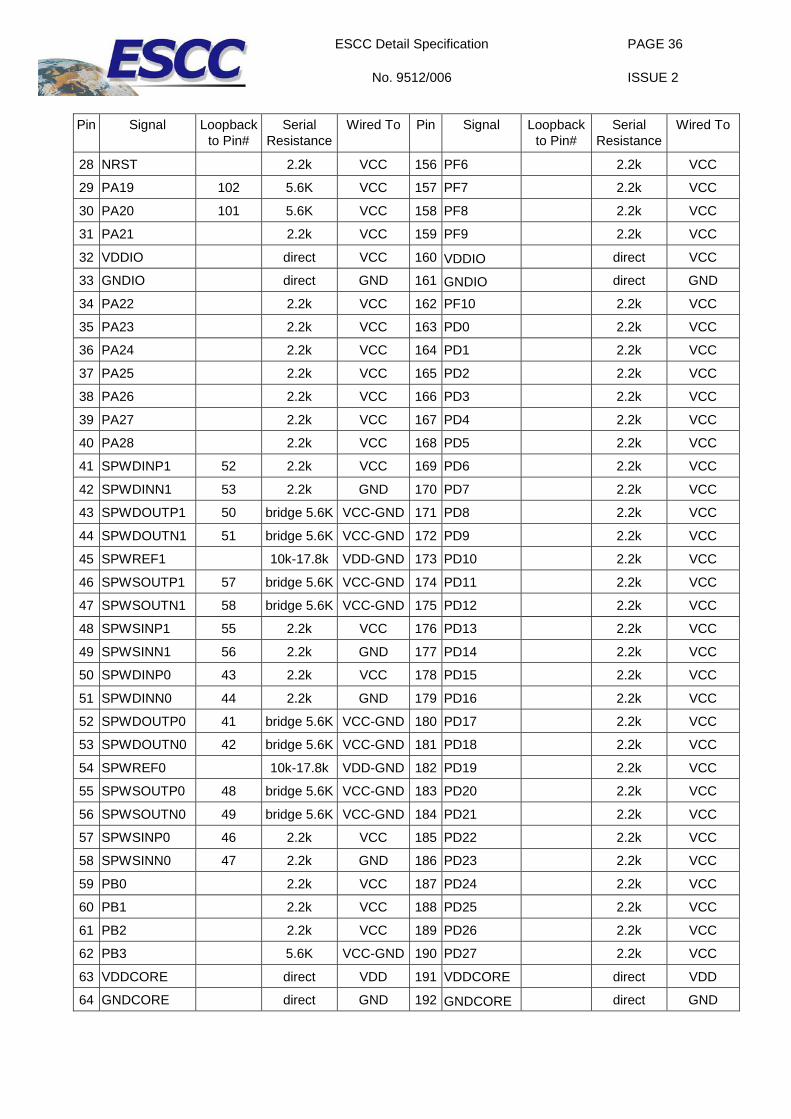
ESCC Detail Specification
No. 9512/006
PAGE 36
ISSUE 2
Pin Signal Loopback
to Pin# Serial
Resistance Wired To Pin Signal Loopback
to Pin# Serial
Resistance Wired To
28 NRST 2.2k VCC 156 PF6 2.2k VCC
29 PA19 102 5.6K VCC 157 PF7 2.2k VCC
30 PA20 101 5.6K VCC 158 PF8 2.2k VCC
31 PA21 2.2k VCC 159 PF9 2.2k VCC
32 VDDIO direct VCC 160 VDDIO direct VCC
33 GNDIO direct GND 161 GNDIO direct GND
34 PA22 2.2k VCC 162 PF10 2.2k VCC
35 PA23 2.2k VCC 163 PD0 2.2k VCC
36 PA24 2.2k VCC 164 PD1 2.2k VCC
37 PA25 2.2k VCC 165 PD2 2.2k VCC
38 PA26 2.2k VCC 166 PD3 2.2k VCC
39 PA27 2.2k VCC 167 PD4 2.2k VCC
40 PA28 2.2k VCC 168 PD5 2.2k VCC
41 SPWDINP1 52 2.2k VCC 169 PD6 2.2k VCC
42 SPWDINN1 53 2.2k GND 170 PD7 2.2k VCC
43 SPWDOUTP1 50 bridge 5.6K VCC-GND 171 PD8 2.2k VCC
44 SPWDOUTN1 51 bridge 5.6K VCC-GND 172 PD9 2.2k VCC
45 SPWREF1 10k-17.8k VDD-GND 173 PD10 2.2k VCC
46 SPWSOUTP1 57 bridge 5.6K VCC-GND 174 PD11 2.2k VCC
47 SPWSOUTN1 58 bridge 5.6K VCC-GND 175 PD12 2.2k VCC
48 SPWSINP1 55 2.2k VCC 176 PD13 2.2k VCC
49 SPWSINN1 56 2.2k GND 177 PD14 2.2k VCC
50 SPWDINP0 43 2.2k VCC 178 PD15 2.2k VCC
51 SPWDINN0 44 2.2k GND 179 PD16 2.2k VCC
52 SPWDOUTP0 41 bridge 5.6K VCC-GND 180 PD17 2.2k VCC
53 SPWDOUTN0 42 bridge 5.6K VCC-GND 181 PD18 2.2k VCC
54 SPWREF0 10k-17.8k VDD-GND 182 PD19 2.2k VCC
55 SPWSOUTP0 48 bridge 5.6K VCC-GND 183 PD20 2.2k VCC
56 SPWSOUTN0 49 bridge 5.6K VCC-GND 184 PD21 2.2k VCC
57 SPWSINP0 46 2.2k VCC 185 PD22 2.2k VCC
58 SPWSINN0 47 2.2k GND 186 PD23 2.2k VCC
59 PB0 2.2k VCC 187 PD24 2.2k VCC
60 PB1 2.2k VCC 188 PD25 2.2k VCC
61 PB2 2.2k VCC 189 PD26 2.2k VCC
62 PB3 5.6K VCC-GND 190 PD27 2.2k VCC
63 VDDCORE direct VDD 191 VDDCORE direct VDD
64 GNDCORE direct GND 192 GNDCORE direct GND
ESCC Detail Specification
No. 9512/006
PAGE 37
ISSUE 2
Pin Signal Loopback
to Pin# Serial
Resistance Wired To Pin Signal Loopback
to Pin# Serial
Resistance Wired To
65 GNDCORE direct GND 193 GNDCORE direct GND
66 VDDCORE direct VDD 194 VDDCORE direct VDD
67 PB4 70 bridge 5.6K VCC-GND 195 PD28 2.2k VCC
68 PB5 69 2.2k VCC 196 PD29 2.2k VCC
69 PB6 68 bridge 5.6K VCC-GND 197 PD30 2.2k VCC
70 PB7 67 2.2k VCC 198 PD31 2.2k VCC
71 PB8 2.2k VCC 199 PG0 5.6K VCC-GND
72 PB9 2.2k VCC 200 PG1 5.6K VCC-GND
73 PB10 2.2k VCC 201 PG2 5.6K VCC-GND
74 PB11 2.2k VCC 202 PG3 5.6K VCC-GND
75 PB12 2.2k VCC 203 PG4 5.6K VCC-GND
76 PB13 2.2k VCC 204 PG5 5.6K VCC-GND
77 PB14 2.2k VCC 205 PG6 5.6K VCC-GND
78 PB15 2.2k VCC 206 PG7 5.6K VCC-GND
79 PB16 5.6K VCC-GND 207 PG8 5.6K VCC-GND
80 XOUT 5.6K VCC-GND 208 PG9 5.6K VCC-GND
81 XIN 2.2k GND 209 PG10 5.6K VCC-GND
82 VDDPLLA direct VDD 210 PG11 5.6K VCC-GND
83 GNDPLLA direct GND 211 PG12 5.6K VCC-GND
84 GNDPLLB direct GND 212 PG13 5.6K VCC-GND
85 VDDPLLB direct VDD 213 PG14 5.6K VCC-GND
86 PB17 2.2k VCC 214 PG15 5.6K VCC-GND
87 PB18 2.2k VCC 215 PG16 5.6K VCC-GND
88 PB19 2.2k VCC 216 PG17 5.6K VCC-GND
89 PB20 2.2k VCC 217 PG18 5.6K VCC-GND
90 PB21 2.2k VCC 218 PG19 5.6K VCC-GND
91 PB22 2.2k VCC 219 PG20 5.6K VCC-GND
92 PB23 2.2k VCC 220 PG21 5.6K VCC-GND
93 PB24 2.2k VCC 221 PG22 5.6K VCC-GND
94 PB25 2.2k VCC 222 PG23 5.6K VCC-GND
95 PB26 2.2k VCC 223 PG24 5.6K VCC-GND
96 VDDIO direct VCC 224 VDDIO direct VCC
97 GNDIO direct GND 225 GNDIO direct GND
98 PB27 2.2k VCC 226 PG25 5.6K VCC-GND
99 PB28 2.2k VCC 227 PG26 5.6K VCC-GND
100 PB29 2.2k VCC 228 PG27 5.6K VCC-GND
101 PC0 30 5.6K VCC 229 XOUT32 5.6K VCC-GND

ESCC Detail Specification
No. 9512/006
PAGE 38
ISSUE 2
Pin Signal Loopback
to Pin# Serial
Resistance Wired To Pin Signal Loopback
to Pin# Serial
Resistance Wired To
102 PC1 29 5.6K VCC 230 XIN32 2.2k GND
103 PC2 2.2k VCC 231 PG30 5.6K VCC-GND
104 PC3 2.2k VCC 232 PG31 5.6K VCC-GND
105 PC4 2.2k VCC 233 PF11 2.2k VCC
106 PC5 2.2k VCC 234 PF12 2.2k VCC
107 PC6 2.2k VCC 235 PF13 2.2k VCC
108 PC7 2.2k VCC 236 PF14 2.2k VCC
109 PC8 2.2k VCC 237 PF15 2.2k VCC
110 PC9 2.2k VCC 238 PF16 2.2k VCC
111 PC10 2.2k VCC 239 PF17 2.2k VCC
112 PC11 2.2k VCC 240 PF18 2.2k VCC
113 PC12 2.2k VCC 241 PF19 2.2k VCC
114 PC13 2.2k VCC 242 PF20 2.2k VCC
115 PC14 2.2k VCC 243 PF21 2.2k VCC
116 PC15 2.2k VCC 244 PF22 2.2k VCC
117 PC16 2.2k VCC 245 PF23 2.2k VCC
118 PC17 2.2k VCC 246 PF24 2.2k GND
119 PC18 2.2k VCC 247 PF25 2.2k VCC
120 PC19 2.2k VCC 248 BTXOUTN 5.6K VCC-GND
121 PC20 122 bridge 5.6K VCC-GND 249 BTXOUTP 5.6K VCC-GND
122 PC21 121 2.2k VCC 250 BRXINN 2.2k GND
123 PC22 2.2k VCC 251 BRXINP 2.2k VCC
124 PC23 2.2k VCC 252 PF26 2.2k VCC
125 PC24 2.2k VCC 253 PF27 16 bridge 5.6K VCC-GND
126 PC25 2.2k VCC 254 PF28 17 bridge 5.6K VCC-GND
127 VDDCORE direct VDD 255 VDDCORE direct VDD
128 GNDCORE direct GND 256 GNDCORE direct GND
2.7 HIGH TEMPERATURE REVERSE BIAS BURN-IN (STATIC BURN-IN) CONDITIONS For the High Temperature Reverse Bias Burn-In, no code needs to be loaded into the Flash. The hardware remains the same as for the Power Burn-In, except for a jumper instead of a 2.2kΩ resistor on pin 28 (NRST).
2.8 OPERATING LIFE CONDITIONS The conditions shall be as specified in Para. 2.6, Power Burn-in Conditions.
ESCC Detail Specification
No. 9512/006
PAGE 39
ISSUE 2
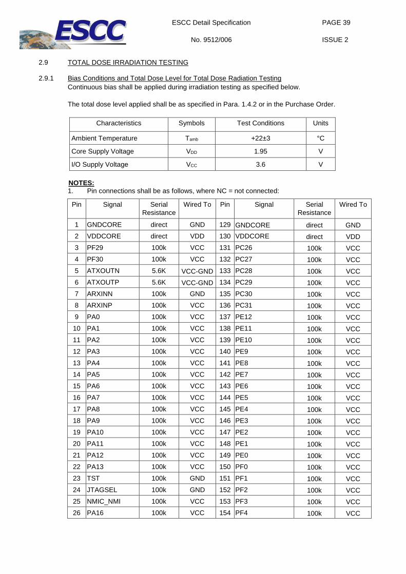
2.9 TOTAL DOSE IRRADIATION TESTING
2.9.1 Bias Conditions and Total Dose Level for Total Dose Radiation Testing Continuous bias shall be applied during irradiation testing as specified below.
The total dose level applied shall be as specified in Para. 1.4.2 or in the Purchase Order.
Characteristics Symbols Test Conditions Units
Ambient Temperature Tamb +22±3 °C
Core Supply Voltage VDD 1.95 V
I/O Supply Voltage VCC 3.6 V
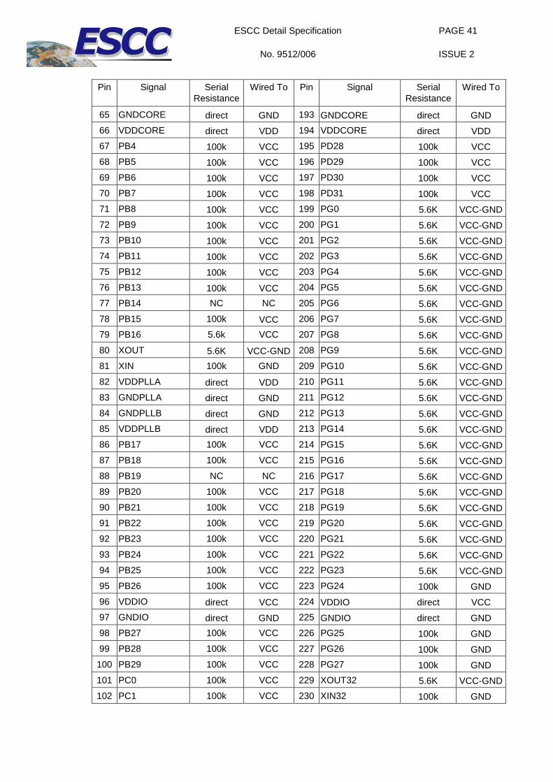
NOTES: 1. Pin connections shall be as follows, where NC = not connected:
Pin Signal Serial Resistance
Wired To Pin Signal Serial Resistance
Wired To
1 GNDCORE direct GND 129 GNDCORE direct GND 2 VDDCORE direct VDD 130 VDDCORE direct VDD 3 PF29 100k VCC 131 PC26 100k VCC 4 PF30 100k VCC 132 PC27 100k VCC 5 ATXOUTN 5.6K VCC-GND 133 PC28 100k VCC 6 ATXOUTP 5.6K VCC-GND 134 PC29 100k VCC 7 ARXINN 100k GND 135 PC30 100k VCC 8 ARXINP 100k VCC 136 PC31 100k VCC 9 PA0 100k VCC 137 PE12 100k VCC 10 PA1 100k VCC 138 PE11 100k VCC 11 PA2 100k VCC 139 PE10 100k VCC 12 PA3 100k VCC 140 PE9 100k VCC 13 PA4 100k VCC 141 PE8 100k VCC 14 PA5 100k VCC 142 PE7 100k VCC 15 PA6 100k VCC 143 PE6 100k VCC 16 PA7 100k VCC 144 PE5 100k VCC 17 PA8 100k VCC 145 PE4 100k VCC 18 PA9 100k VCC 146 PE3 100k VCC 19 PA10 100k VCC 147 PE2 100k VCC 20 PA11 100k VCC 148 PE1 100k VCC 21 PA12 100k VCC 149 PE0 100k VCC 22 PA13 100k VCC 150 PF0 100k VCC 23 TST 100k GND 151 PF1 100k VCC 24 JTAGSEL 100k GND 152 PF2 100k VCC 25 NMIC_NMI 100k VCC 153 PF3 100k VCC 26 PA16 100k VCC 154 PF4 100k VCC

ESCC Detail Specification
No. 9512/006
PAGE 40
ISSUE 2
Pin Signal Serial
Resistance Wired To Pin Signal Serial
Resistance Wired To
27 PA17 100k VCC 155 PF5 100k VCC 28 NRST direct (*) 156 PF6 100k VCC 29 PA19 100k VCC 157 PF7 100k VCC 30 PA20 100k VCC 158 PF8 100k VCC 31 PA21 100k VCC 159 PF9 100k VCC 32 VDDIO direct VCC 160 VDDIO direct VCC 33 GNDIO direct GND 161 GNDIO direct GND 34 PA22 100k VCC 162 PF10 100k VCC 35 PA23 100k VCC 163 PD0 100k VCC 36 PA24 100k VCC 164 PD1 100k VCC 37 PA25 100k VCC 165 PD2 100k VCC 38 PA26 100k VCC 166 PD3 100k VCC 39 PA27 100k VCC 167 PD4 100k VCC 40 PA28 100k VCC 168 PD5 100k VCC 41 SPWDINP1 100k VCC 169 PD6 100k VCC 42 SPWDINN1 100k GND 170 PD7 100k VCC 43 SPWDOUTP1 5.6K VCC-GND 171 PD8 100k VCC 44 SPWDOUTN1 5.6K VCC-GND 172 PD9 100k VCC 45 SPWREF1 direct VDD 173 PD10 100k VCC 46 SPWSOUTP1 5.6K VCC-GND 174 PD11 100k VCC 47 SPWSOUTN1 5.6K VCC-GND 175 PD12 100k VCC 48 SPWSINP1 100k VCC 176 PD13 100k VCC 49 SPWSINN1 100k GND 177 PD14 100k VCC 50 SPWDINP0 100k VCC 178 PD15 100k VCC 51 SPWDINN0 100k GND 179 PD16 100k VCC 52 SPWDOUTP0 5.6K VCC-GND 180 PD17 100k VCC 53 SPWDOUTN0 5.6K VCC-GND 181 PD18 100k VCC 54 SPWREF0 direct VDD 182 PD19 100k VCC 55 SPWSOUTP0 5.6K VCC-GND 183 PD20 100k VCC 56 SPWSOUTN0 5.6K VCC-GND 184 PD21 100k VCC 57 SPWSINP0 100k VCC 185 PD22 100k VCC 58 SPWSINN0 100k GND 186 PD23 100k VCC 59 PB0 100k VCC 187 PD24 100k VCC 60 PB1 100k VCC 188 PD25 100k VCC 61 PB2 100k VCC 189 PD26 100k VCC 62 PB3 5.6K VCC-GND 190 PD27 100k VCC 63 VDDCORE direct VDD 191 VDDCORE direct VDD 64 GNDCORE direct GND 192 GNDCORE direct GND
ESCC Detail Specification
No. 9512/006
PAGE 41
ISSUE 2
Pin Signal Serial
Resistance Wired To Pin Signal Serial
Resistance Wired To
65 GNDCORE direct GND 193 GNDCORE direct GND 66 VDDCORE direct VDD 194 VDDCORE direct VDD 67 PB4 100k VCC 195 PD28 100k VCC 68 PB5 100k VCC 196 PD29 100k VCC 69 PB6 100k VCC 197 PD30 100k VCC 70 PB7 100k VCC 198 PD31 100k VCC 71 PB8 100k VCC 199 PG0 5.6K VCC-GND 72 PB9 100k VCC 200 PG1 5.6K VCC-GND 73 PB10 100k VCC 201 PG2 5.6K VCC-GND 74 PB11 100k VCC 202 PG3 5.6K VCC-GND 75 PB12 100k VCC 203 PG4 5.6K VCC-GND 76 PB13 100k VCC 204 PG5 5.6K VCC-GND 77 PB14 NC NC 205 PG6 5.6K VCC-GND 78 PB15 100k VCC 206 PG7 5.6K VCC-GND 79 PB16 5.6k VCC 207 PG8 5.6K VCC-GND 80 XOUT 5.6K VCC-GND 208 PG9 5.6K VCC-GND 81 XIN 100k GND 209 PG10 5.6K VCC-GND 82 VDDPLLA direct VDD 210 PG11 5.6K VCC-GND 83 GNDPLLA direct GND 211 PG12 5.6K VCC-GND 84 GNDPLLB direct GND 212 PG13 5.6K VCC-GND 85 VDDPLLB direct VDD 213 PG14 5.6K VCC-GND 86 PB17 100k VCC 214 PG15 5.6K VCC-GND 87 PB18 100k VCC 215 PG16 5.6K VCC-GND 88 PB19 NC NC 216 PG17 5.6K VCC-GND 89 PB20 100k VCC 217 PG18 5.6K VCC-GND 90 PB21 100k VCC 218 PG19 5.6K VCC-GND 91 PB22 100k VCC 219 PG20 5.6K VCC-GND 92 PB23 100k VCC 220 PG21 5.6K VCC-GND 93 PB24 100k VCC 221 PG22 5.6K VCC-GND 94 PB25 100k VCC 222 PG23 5.6K VCC-GND 95 PB26 100k VCC 223 PG24 100k GND 96 VDDIO direct VCC 224 VDDIO direct VCC 97 GNDIO direct GND 225 GNDIO direct GND 98 PB27 100k VCC 226 PG25 100k GND 99 PB28 100k VCC 227 PG26 100k GND 100 PB29 100k VCC 228 PG27 100k GND 101 PC0 100k VCC 229 XOUT32 5.6K VCC-GND 102 PC1 100k VCC 230 XIN32 100k GND
ESCC Detail Specification
No. 9512/006
PAGE 42
ISSUE 2
Pin Signal Serial
Resistance Wired To Pin Signal Serial
Resistance Wired To
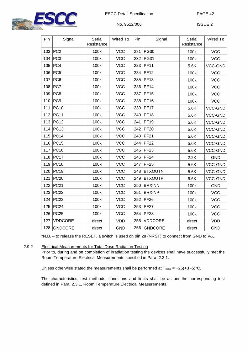
103 PC2 100k VCC 231 PG30 100k VCC 104 PC3 100k VCC 232 PG31 100k VCC 105 PC4 100k VCC 233 PF11 5.6K VCC-GND 106 PC5 100k VCC 234 PF12 100k VCC 107 PC6 100k VCC 235 PF13 100k VCC 108 PC7 100k VCC 236 PF14 100k VCC 109 PC8 100k VCC 237 PF15 100k VCC 110 PC9 100k VCC 238 PF16 100k VCC 111 PC10 100k VCC 239 PF17 5.6K VCC-GND 112 PC11 100k VCC 240 PF18 5.6K VCC-GND 113 PC12 100k VCC 241 PF19 5.6K VCC-GND 114 PC13 100k VCC 242 PF20 5.6K VCC-GND 115 PC14 100k VCC 243 PF21 5.6K VCC-GND 116 PC15 100k VCC 244 PF22 5.6K VCC-GND 117 PC16 100k VCC 245 PF23 5.6K VCC-GND 118 PC17 100k VCC 246 PF24 2.2K GND 119 PC18 100k VCC 247 PF25 5.6K VCC-GND 120 PC19 100k VCC 248 BTXOUTN 5.6K VCC-GND 121 PC20 100k VCC 249 BTXOUTP 5.6K VCC-GND 122 PC21 100k VCC 250 BRXINN 100k GND 123 PC22 100k VCC 251 BRXINP 100k VCC 124 PC23 100k VCC 252 PF26 100k VCC 125 PC24 100k VCC 253 PF27 100k VCC 126 PC25 100k VCC 254 PF28 100k VCC 127 VDDCORE direct VDD 255 VDDCORE direct VDD 128 GNDCORE direct GND 256 GNDCORE direct GND
*N.B. – to release the RESET, a switch is used on pin 28 (NRST) to connect from GND to VCC.
2.9.2 Electrical Measurements for Total Dose Radiation Testing Prior to, during and on completion of irradiation testing the devices shall have successfully met the Room Temperature Electrical Measurements specified in Para. 2.3.1.
Unless otherwise stated the measurements shall be performed at Tcase = +25(+3 -5)°C.
The characteristics, test methods, conditions and limits shall be as per the corresponding test defined in Para. 2.3.1, Room Temperature Electrical Measurements.
Related Documents