Sensors and Materials, Vol. 12 , No. 5 (2000) 233-288 MYU Tokyo S&M0409 Inared Detectors at the Beginning of the Next Millennium Antoni Rogalski Institute of Applied Physics, Mility University of Technology, 2 Kalisego Str., 00-908 Wsaw, Pold (Received July 17, 2000; accepted September 8, 2000) Key words: infrared detectors, HgCdTe photodiodes, QWIPs, thermal detectors, ROICs, cal ple ays, two-colour detectors. At present efforts in infrared (IR) detector research are directed towards improving the performance of single element devices and large electronically scanned arrays and obtaining a higher operating temperature of detectors. Another important aim is to make IR detectors cheaper and more convenient to use. Recent progress in different IR technologies is described from a historical point of view. Discussion is concentrated mainly on current and most rapidly developing detectors: HgCdTe heterostructure photo- diodes, quantum well AlGaAs/GaAs and thermal detectors. The outlook r near-future trends in IR technologies is also presented. 1. Introduction Looking back over the past 1000 years, we notice that inared (IR) itself was unknown until 200 years ago when Herschel's experiment with the thermometer was first reported. O) Following the work of Kirchhoff, Stefan, Boltzman, Wien and Rayleigh, Max Planck culminated the effort with the well-known Planck's law. The early history of IR was reviewed about 40 years ago in two well-known monographs.< 2 - 3 ) Many materials have been investigated in the IR field. After observing the history of the development of IR detector technology, a simple theorem can be stated: <4l All physical phenomena in the range of about 0.1-1 e V can be proposed for IR detectors. Among these effects are: thermoelectric power (thermocouples), change in electrical conductivity (bolometers), gas expansion (Golay cell), pyroelectricity (pyroelectric detectors), photon drag, Josephson effect (Josephson junctions, SQUIDs), inteal emission (PtSi Schottky 233

Welcome message from author
This document is posted to help you gain knowledge. Please leave a comment to let me know what you think about it! Share it to your friends and learn new things together.
Transcript
Sensors and Materials, Vol. 12 , No. 5 (2000) 233-288 MYU Tokyo
S&M0409
Infrared Detectors at the Beginning
of the Next Millennium
Antoni Rogalski
Institute of Applied Physics, Military University of Technology, 2 Kaliskiego Str., 00-908 Warsaw, Poland
(Received July 17, 2000; accepted September 8, 2000)
Key words: infrared detectors, HgCdTe photodiodes, QWIPs, thermal detectors, ROICs, focal plane arrays, two-colour detectors.
At present efforts in infrared (IR) detector research are directed towards improving the performance of single element devices and large electronically scanned arrays and
obtaining a higher operating temperature of detectors. Another important aim is to make
IR detectors cheaper and more convenient to use. Recent progress in different IR technologies is described from a historical point of view. Discussion is concentrated mainly on current and most rapidly developing detectors: HgCdTe heterostructure photodiodes, quantum well AlGaAs/GaAs and thermal detectors. The outlook for near-future trends in IR technologies is also presented.
1. Introduction
Looking back over the past 1000 years, we notice that infrared (IR) itself was unknown until 200 years ago when Herschel's experiment with the thermometer was first reported. O) Following the work of Kirchhoff, Stefan, Boltzman, Wien and Rayleigh, Max
Planck culminated the effort with the well-known Planck's law. The early history of IR was reviewed about 40 years ago in two well-known monographs.<2-3)
Many materials have been investigated in the IR field. After observing the history of the development of IR detector technology, a simple theorem can be stated:<4l All physical
phenomena in the range of about 0.1-1 e V can be proposed for IR detectors. Among these effects are: thermoelectric power (thermocouples), change in electrical conductivity (bolometers), gas expansion (Golay cell), pyroelectricity (pyroelectric detectors), photon
drag, Josephson effect (Josephson junctions, SQUIDs), internal emission (PtSi Schottky
233
� 1! f-
234 Sensors and Materials, Vol. 12, No. 5 (2000)
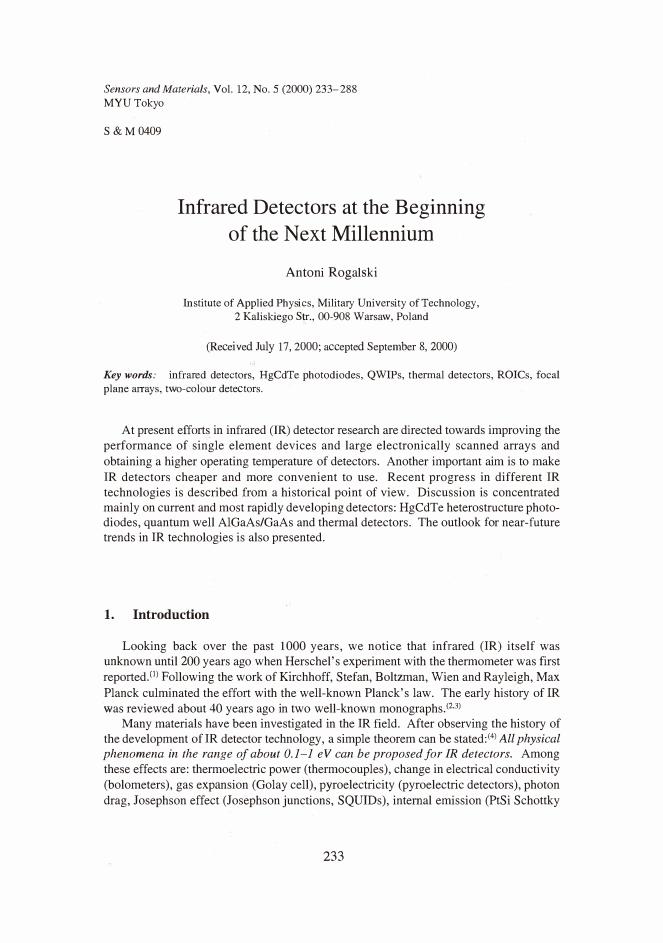
barriers), fundamental absorption (intrinsic photodetectors), impurity absorption (extrinsic photodetectors), low dimensional solids (superlattice (SL) and quantum well (QW) detectors), different types of phase transitions and others. Figure 1 gives approximate dates of significant development efforts for the materials mentioned.
In this article a review of the current status and future trends in IR detector technologies is presented, taking into account a historical perspective of their development. Special attention is directed towards the most rapidly developing detectors: HgCdTe heterostructure photodiodes, quantum well AlGaAs/GaAs, and thermal detectors. Finally, the anticipated evolution of IR technology in the next ten years is presented.
2. Historical Background
The thermometer was the first of a trio of thermal detectors that were to dominate the IR detector field until World War I.<5lJn 1821, Seebeck discovered the thermoelectric effect and soon thereafter demonstrated the first thermocouple. In 1829, Nobili constructed the first thermopile by connecting a number of thermocouples in a series. Macedonio Melloni helped him modify the design of series-connected thermocouples in 1833.<6) The third member of the trio, Langley's bolometer, appeared in 1881.(7) Langley made the first resistive bolometer of platinum strips in a Wheatstone bridge, which he worked on for 20 years, when he demonstrated that the device exhibited a deflection from a cow one-quarter of a mile away.
The material T}zS was the first IR photoconductor of high responsivity and was developed by Case in 1917. cs) The development of photon IR detectors began with lead sulphide in the 1930s. The years during World War II saw the origin of modern IR detector technology. Photon IR technology combined with semiconductor material science, photolithography technology developed for integrated circuits, and the impetus of Cold War military preparedness have propelled extraordinary advances in IR capabilities in only a fraction of this century.
During the 1950s, IR detectors were built using single-element-cooled lead salt detectors, primarily for anti-air-missile seekers. Usually lead salt detectors were polycrystalline and were produced by vacuum evaporation and chemical deposition from a
., X.c '; �
"'" 22 Q) U) '.;, �?;5 ;::: a. a. CJ-= :,:: a."'
� l l 11 l 1 l1940 1950 1960 1970 1980 1990 2000
Fig. 1. History of the development of infrared detectors.
Sensors and Materials, Vol. 12, No. 5 (2000) 235
solution, followed by a post-growth sensitisation process_C9l The first extrinsic photoconductive detectors were reported in the early 1950s. Since the techniques for controlled impurity introduction became available for germanium at an earlier date, the first highperformance extrinsic detectors were based on germanium. Extrinsic photoconductive response from copper, zinc and gold impurity levels in germanium gave rise to devices using the 8 to 14 µm long wavelength IR (L WIR) spectral window and beyond to the 14 to 30 µm very long wavelength IR (VL WIR) region. Extrinsic photoconductors were widely used at wavelengths beyond 10 µm prior to the development of the intrinsic detectors. They must be operated at lower temperatures to achieve performance similar to that of intrinsic detectors, and a sacrifice in quantum efficiency is required to avoid impracticably thick detectors. Although Si has several advantages over Ge (namely, a lower dielectric constant giving a shorter dielectric relaxation time and lower capacitance, a higher dopant solubility and larger photoionization cross section for higher quantum efficiency, and a lower refractive index for lower reflectance), these were not sufficient to warrant the necessary development efforts needed to bring it to the level of the, by then, highly developed Ge detectors. After being dormant for about ten years, extrinsic Si was reconsidered after the invention of charge-coupled devices (CCDs) by Boyle and Smith.0°l In 1973, Shepherd and Yang(11J proposed the metal-silicide/silicon Schottky-barrier detectors. For the first time it became possible to have highly sophisticated readout schemes - both detection and readout could be implemented on one common silicon chip.
At the same time, rapid advances were being made in narrow bandgap semiconductorsthat would later prove useful in extending wavelength capabilities and improving sensitivity. The first such material was InSb, a member of the newly discovered III-V compound semiconductor family. The end of the 1950s saw the introduction of semiconductor alloys in III-V, IV-VI, and II-VI material systems. These alloys allowed the bandgap of the semiconductor and hence the spectral response of the detector to be custom tailored for specific applications. In 1959, research by Lawson et al.02
) triggered the development of variable bandgap Hg1 _ xCdxTe (HgCdTe) alloys, providing an unprecedented degree of freedom in infrared detector design.
The fundamental properties of narrow-gap semiconductors (high optical absorption coefficient, high electron mobility and low thermal generation rate), together with the capability for bandgap engineering, make these alloy systems almost ideal for a wide range of IR detectors. The material technology development was and continues to be primarily for military applications. A negative aspect of support by defence agencies has been the associated secrecy requirements that inhibit meaningful collaborations among research teams on a national and especially on an international level. In addition, the primary focus has been on focal plane array (FPA) demonstration and much less on establishing the knowledge base. Nevertheless, significant progress has been made over three decades. At present, HgCdTe is the most widely used variable gap semiconductor for IR photodetectors. Over the years it has successfully fought off major challenges from extrinsic silicon and lead-tin telluride devices, but despite that it has more competitors today than ever before. These include Schottky barriers on silicon, SiGe heterojunctions, AlGaAs multiple quantum wells, GainSb strain layer superlattices, high-temperature
superconductors and especially two types of thermal detectors: pyroelectric detectors and silicon bolometers. It is interesting, however, that none of these competitors can compete
236 Sensors and Materials, Vol. 12, No. 5 (2000)
in terms of fundamental properties. They may promise to have greater manufacturability, but never to provide higher performance or, with the exception of thermal detectors, operate at higher or even comparable temperatures.
It must not be inferred from the preceding outline that work on thermardetectors has
not also been actively pursued. Some interesting and important developments have taken place along these lines. In 1947, for example, Golay constructed an improved pneumatic infrared detectorY3) The thermistor bolometer, originally developed by Bell TelephoneLaboratories, has found widespread use iq detecting radiation from low temperature sources.<14
J The superconducting effect has been used in making extremely sensitive bolometers.
Thermal detectors have also been used for infrared imaging. Evaporographs and
absorption edge image converters were among the first non-scanned IR imagers. Originally an evaporograph was employed in which the radiation was focused onto a blackened membrane coated with a thin film of oil.05) The differential rate of evaporation of the oilwas proportional to radiation intensity. The film was then illuminated with visible light to produce an interference pattern corresponding to the thermal picture. The second thermal imaging device was the absorption edge image converterY6) Operation of the device was
based upon utilising the temperature dependence of the location of the absorption edge of the semiconductor. The performance of both imaging devices was poor because of the
very long time constant and the poor spatial resolution. Despite numerous research initiatives and the attractions of ambient temperature operation and low cost potential, thermal detector technology has enjoyed limited success in competition with cooled photon detectors for thermal imaging applications. A notable exception is the pyroelectric vidicon (PEV),<17
J which is widely used by firefighting and emergency service
organisations. The pyroelectric vidicon tube can be considered as being analogous to the visible television camera tube except that the photoconductive target is replaced by a
pyroelectric detector and germanium faceplate. Compact, rugged PEV imagers have been offered for military applications but suffer the disadvantage of low tube life and fragility, particularly the reticulated vidicon tubes required for enhanced spatial resolution.
The second revolution in thermal imaging is underway now. Although thermal detectors have been little used in scanned imagers because of their slow response, they are currently of considerable interest for two-d.imensional electronically addressed arrays
where the bandwidth is low and the ability of thermal devices to integrate over a frame
time is an advantage.<1B-20J Much recent research has focused on both hybrid and monolithic uncooled arrays and has yielded significant improvements in the detectivity of both bolometric and pyroelectric detector arrays.
3. Classification of Infrared Detectors
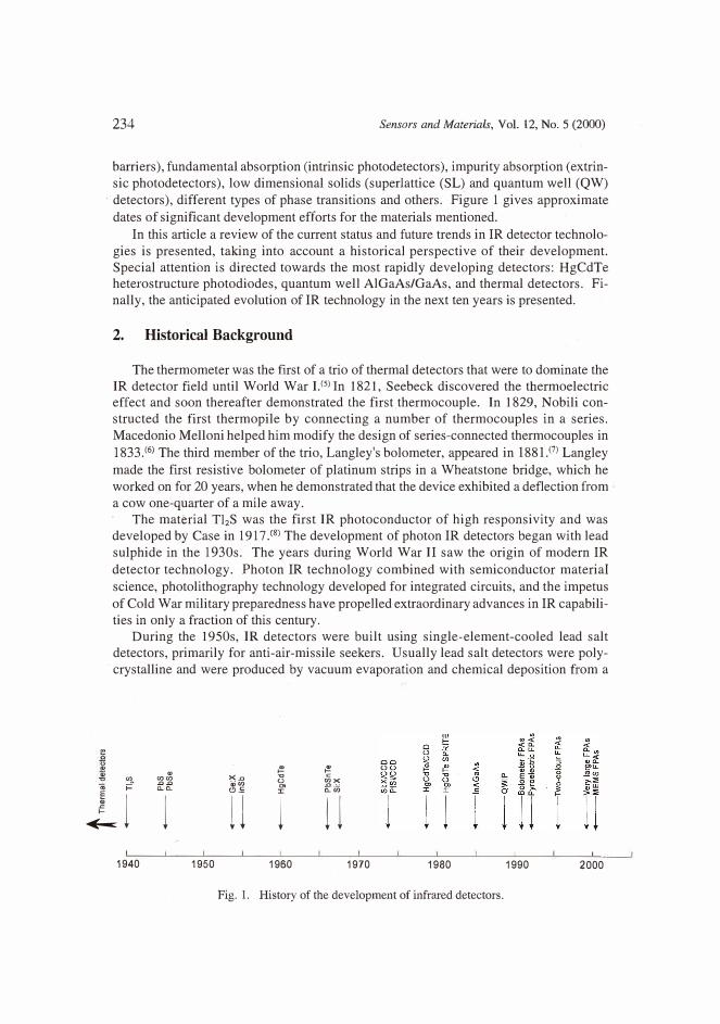
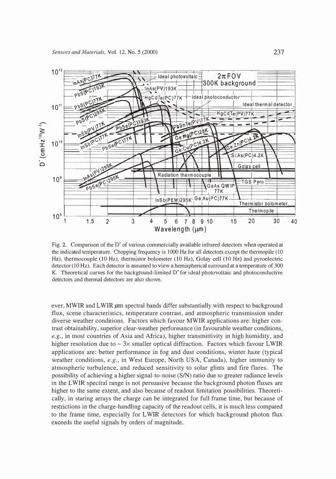
Spectral detectivity curves for a number of commercially available IR detectors are shown in Fig. 2. Interest has centred mainly on the wavelengths of the two atmospheric windows 3-5 µm (middle wavelength IR (MWIR)) and 8-14 µm (LWIR region) (atmospheric transmission is the highest in these bands and the emissivity maximum of the objects at T"" 300 K is at the wavelength A"" 10 micron), though in recent years there has been increasing interest in longer wavelengths stimulated by space applications. How-
-
? N
I
E
� Cl
Sensors and Materials, Vol. 12, No. 5 (2000)
1012
� \.r'c111¥-- �
�,"r,,.s_ �
� --[\.'lr;,?,V..- ?'o$\.'<'
r-: /
' � Ideal photovoltaic� 21tFOV ,I I I
lnAs(PV}193K -,. ' I I
300K background I I I
r-ldeal photoconductor
237
1011 =? c,11¥--�..,.....�'()$\? -�-
Hgi:,2
e(PC}77K-� J ' ...... I L----r I Ideal thermal detector
1010
109
108
� '��i:;,'f: �fc,-i: � • - 1usl0. i- .- _.. S1r;,?J¥-- -
?\l:(\'f... ?� =--,"s'o 1'i-�c," 1c,11'f...
== '"s�,_?'o$e� -
--
.
�
-
.
I
.... :::;; ,,,
.-
�r>\Jyri¥--'oS"ie �
�)2.si, "'"' ·\-\91.?C -...L.� 'f-J
-Cll�?Clb, .1
Ge- -,,.
\
HgC'!Je(PV)77K - ,--,,--- -
- - I -- -1 --
�- - ��t?:'c� <i."'? � e-
- Si:As(PC}4.2KI I
-
'J,�i:;i'i-./' .,,,,,.. --- /' I\ ' Golav cell I�\I � '"i,-s 2.��'f-.
-,1c
?'ose
/
1 1.5 2 3
\ Radiation thermocouple I
I I I
.. .� TGS Pyro GaAsQWIP . 77K I
\ I\ I
\ '
lnS b(P EM }295K-G e:Au(P C)77K- I 111 Thermistor bolometer
.... 1' Thermopile
4 5 6 7 8 9 10 15 20 30
Wavelength (µm)
Fig. 2. Comparison of the D' of various commercially available infrared detectors when operated atthe indicated temperature. Chopping frequency is 1000 Hz for all detectors except the thermopile (10 Hz), thermocouple (10 Hz), thermistor bolometer (10 Hz), Golay cell (10 Hz) and pyroelectricdetector (10 Hz). Each detector is assumed to view a hemispherical surround at a temperature of 300K. Theoretical curves for the background-limited D' for ideal photovoltaic and photoconductivedetectors and thermal detectors are also shown.
ever, MWIR and LWIR µm spectral bands differ substantially with respect to backgroundflux, scene characteristics, temperature contrast, and atmospheric transmission underdiverse weather conditions. Factors which favour MWIR applications are: higher contrast obtainability, superior clear-weather performance (in favourable weather conditions,e.g., in most countries of Asia and Africa), higher transmittivity in high humidity, andhigher resolution due to - 3x smaller optical diffraction. Factors which favour L WIRapplications are: better performance in fog and dust conditions, winter haze (typicalweather conditions, e.g., in West Europe, North USA, Canada), higher immunity toatmospheric turbulence, and reduced sensitivity to solar glints and fire flares. Thepossibility of achieving a higher signal-to0noise (SIN) ratio due to greater radiance levelsin the LWIR spectral range is not persuasive because the background photon fluxes arehigher to the same extent, and also because of readout limitation possibilities. Theoretically, in staring arrays the charge can be integrated for full frame time, but because ofrestrictions in the charge-handling capacity of the readout cells, it is much less comparedto the frame time, especially for L WIR detectors for which background photon fluxexceeds the useful signals by orders of magnitude.
�
40
238 Sensors and Materials, Vol. 12, No. 5 (2000)
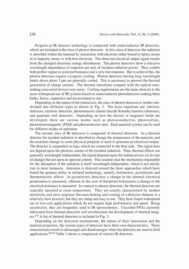
Progress in IR detector technology is connected with semiconductor IR detectors, which are included in the class of photon detectors. In this class of detectors the radiation is absorbed within the material by interaction with electrons either bound to lattice atoms or to impurity atoms or with free electrons. The observed electrical output signal results from the changed electronic energy distribution. The photon detectors show a selective wavelength dependence of response per unit of incident radiation power. They exhibit both perfect signal-to-noise performance and a very fast response. But to achieve this, the photon detectors require cryogenic cooling. Photon detectors having long-wavelength limits above about 3 µm are generally cooled. This is necessary to prevent the thermal generation of charge carriers. The thermal transitions compete with the optical ones, making noncooled devices very noisy. Cooling requirements are the main obstacle to the more widespread use of IR systems based on semiconductor photodetectors making them bulky, heavy, expensive and inconvenient to use.
Depending on the nature of the interaction, the class of photon detectors is further subdivided into different types as shown in Fig. 3. The most important are: intrinsic detectors, extrinsic detectors, photoemissive (metal silicide Schottky baJTiers) detectors, and quantum well detectors. Depending on how the electric or magnetic fields are developed, there are various modes such as photoconductive, photovoltaic, photoelectromagnetic (PEM) and photoemissive ones. Each material system can be used for different modes of operation.
The second class of IR detectors is composed of thermal detectors. In a thermal detector the incident radiation is absorbed to change the temperature of the material, and the resultant change in some physical property is used to generate an electrical output. The detector is suspended on legs, which are connected to the heat sink. The signal does not depend upon the photonic nature of the incident radiation. Thus, thermal effects are generally wavelength independent; the signal depends upon the radiant power (or its rate of change) but not upon its spectral content. This assumes that the mechanism responsible for the absorption of the radiation is itself wavelength independent, which is not strictly true in most instances. Attention is directed toward the three approaches which have found the greatest utility in infrared technology, namely, bolometers, pyroelectric and thermoelectric effects. In pyroelectric detectors a change in the internal electrical polarisation is measured, whereas in the case of thermistor bolometers a change in the electrical resistance is measured. In contrast to photon detectors, the thermal detectors are typically operated at room temperature. They are usually characterised by modest sensitivity and slow response (because heating and cooling of a detector element is a relatively slow process), but they are cheap and easy to use. They have found widespread use in low-cost applications which do not require high performance and speed. Being unselective, they are frequently used in IR spectrometers. Uncooled FPAs currently fabricated from thermal detectors will revolutionise the development ofthernial imagers.<21> A list of thermal detectors is included in Fig. 3.
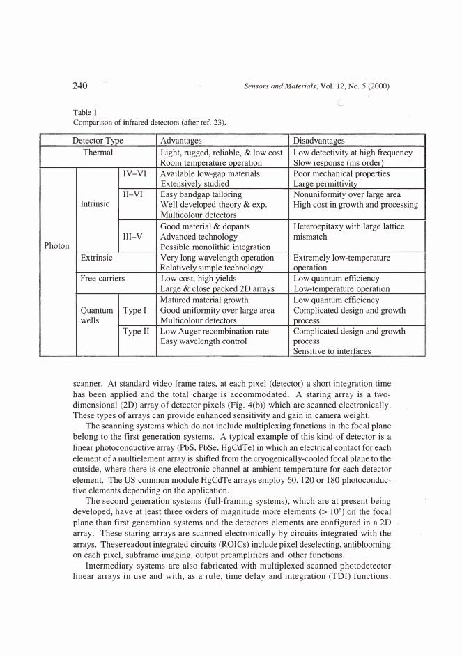
Depending on the detection mechanisms, the nature of their interaction and the material properties, the various types of detectors have their own characteristics. These characteristics result in advantages and disadvantages when the detectors are used in field applications.<22·23l Table 1 shows a comparison of various IR detectors.
Sensors and Materials, Vol. 12, No. 5 (2000)
Infrared detectors
Thermal detectors
Photon detectors
Thermocouple/Thermopile
Bolometers
Pyroelectric/Ferroelectric
Intrinsic
Free carriers
Quantum wells
Photoemissive (P!Si,Pt,Si,lrSi)
Photoconductive (GaAs/AIGaAs)
Photovoltaic (lnAs/lnGaSb,lnAs/lnAsSb)
Fig. 3. Classification of infrared detectors.
4. Focal Plane Arrays
239
There are many important military and civilian applications of IR detectors, which are
frequently called "dual technology applications." Lately, one should point out the
growing utilisation of IR technologies in the civilian sphere at the expense of new
materials and technologies and also the noticeable price decrease in these high-cost
technologies. Demands to use these technologies are quickly growing due to their
effective applications, e.g., in global monitoring of environmental pollution and climate changes, long time prognoses of agriculture crop yields, chemical process monitoring, Fourier transform IR spectroscopy, IR astronomy, car driving, IR imaging in medical
diagnostics, and others. Traditionally, IR technologies have been connected with control
ling functions and night vision problems, with earlier applications connected simply with
detection of IR radiation, and late by forming IR images from temperature and emissivity
differences (systems for recognition and surveillance, tank sight systems, antitank mis
siles, air-air missiles).
Two families of multielement detectors can be considered for principal military and
civilian IR applications; one is used for scanning systems and the other is used for staring
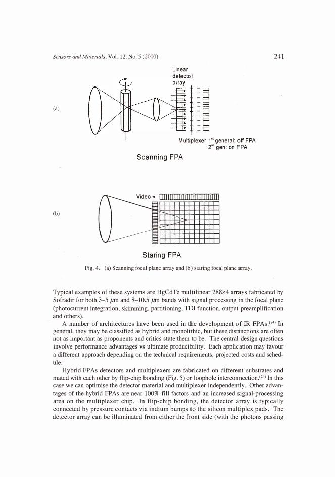
systems. The simplest scanning linear FPA consists of a row of detectors (Fig. 4(a)). An
image is generated by scanning the scene across the strip using, as a rule, a mechanical
Photon
240 Sensors and Materials, Vol. 12, No. 5 (2000)
Table 1
Comparison of infrared detectors (after ref. 23).
Detector Type Advantages Disadvantages
Thermal Light, rugged, reliable, & low cost Low detectivity at high frequency Room temperature operation Slow response (ms order)
IV-VI Available low-gap materials Poor mechanical properties Extensively studied Large permittivity
II-VI Easy bandgap tailoring Nonuniformity over large area Intrinsic Well developed theory & exp. High cost in growth and processing
Multicolour detectors
Good material & dopants Heteroepitaxy with large lattice III-V Advanced technology mismatch
Possible monolithic integration Extrinsic Very long wavelength operation Extremely low-temperature
Relatively simple technology operation Free carriers Low-cost, high yields Low quantum efficiency
Large & close packed 2D arrays Low-temperature operation Matured material growth Low quantum efficiency
Quantum Type I Good unifonnity over large area Complicated design and growth wells Multicolour detectors process
Type II Low Auger recombination rate Complicated design and growth Easy wavelength control process
Sensitive to interfaces
scanner. At standard video frame rates, at each pixel (detector) a short integration time has been applied and the total charge is accommodated. A staring array is a twodimensional (2D) array of detector pixels (Fig. 4(b)) which are scanned electronically. These types of arrays can provide enhanced sensitivity and gain in camera weight.
The scanning systems which do not include multiplexing functions in the focal plane belong to the first generation systems. A typical example of this kind of detector is a linear photoconductive array (PbS, PbSe, HgCdTe) in which an electrical contact for each element of a multielement array is shifted from the cryogenically-cooled focal plane to the outside, where there is one electronic channel at ambient temperature for each detector element. The US common module HgCdTe arrays employ 60, 120 or 180 photoconductive elements depending on the application.
The second generation systems (full-framing systems), which are at present being developed, have at least three orders of magnitude more elements (> 106) on the focal plane than first generation systems and the detectors elements are configured iri a 2D array. These staring arrays are scanned electronically by circuits integrated with the arrays. These readout integrated circuits (ROICs) include pixel deselecting, antibloorning on each pixel, subframe imaging, output preamplifiers and other functions.
Intermediary systems are also fabricated with multiplexed scanned photodetector linear arrays in use and with, as a rule, time delay and integration (TDI) functions.
Sensors and Materials, Vol. 12, No. 5 (2000)
(a)
(b)
Linear detector
Multiplexer 1st
general: off FPA 2
nd
gen: on FPA
Scanning FPA
�+-11111111111111111111111111111 --
-
-
�
Staring FPA
Fig. 4. (a) Scanning focal plane array and (b) staring focal plane array.
241
Typical examples of these systems are HgCdTe multilinear 288x4 arrays fabricated by Sofradir for both 3-5 µm and 8-10.5 µm bands with signal processing in the focal plane(photocurrent integration, skimming, partitioning, TDI function, output preamplificationand others).
A number of architectures have been used in the development of IR FPAs.<24l Ingeneral, they may be classified as hybrid and monolithic, but these distinctions are often
· not as important as proponents and critics state them to be. The central design questionsinvolve performance advantages vs ultimate producibility. Each application may favoura different approach depending on the technical requirements, projected costs and schedule.
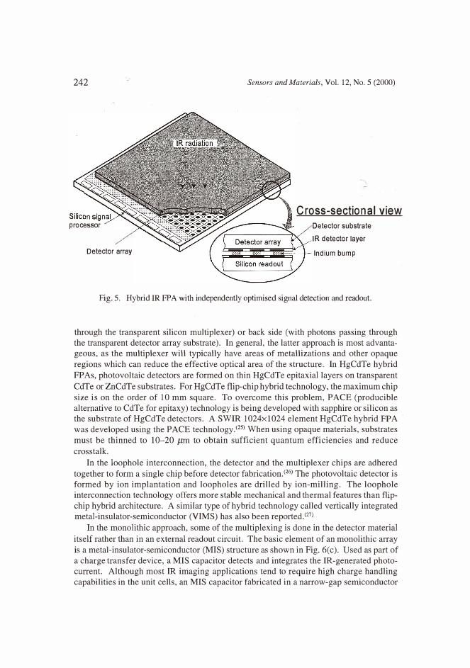
Hybrid FP As detectors and multiplexers are fabricated on different substrates andmated with each other by flip-chip bonding (Fig. 5) or loophole interconnection.<24l In thiscase we can optimise the detector material and multiplexer independently. Other advantages of the hybrid FPAs are near 100% fill factors and an increased signal-processingarea on the multiplexer chip. In flip-chip bonding, the detector array is typicallyconnected by pressure contacts via indium bumps to the silicon multiplex pads. Thedetector array can be illuminated from either the front side (with the photons passing
242
processor
Detector array
Sensors and Materials, Vol. 12, No. 5 (2000)
Cross-sectional view
Detector substrate
IR detector layer
Indium bump
Fig. 5. Hybrid IR FP A with independently optimised signal detection and readout.
through the transparent silicon multiplexer) or back side (with photons passing through the transparent detector array substrate). In general, the latter approach is most advantageous, as the multiplexer will typically have areas of metallizations and other opaque regions which can reduce the effective optical area of the structure. In HgCdTe hybrid
FPAs, photovoltaic detectors are formed on thin HgCdTe epitaxial layers on transparent
CdTe or ZnCdTe substrates. For HgCdTe flip-chip hybrid technology, the maximum chip
size is on the order of 10 mm square. To overcome this problem, PACE (producible alternative to CdTe for epitaxy) technology is being developed with sapphire or silicon as the substrate of HgCdTe detectors. A SWIR 1024x1024 element HgCdTe hybrid FPA was developed using the PACE technology.<25) When using opaque materials, substrates
must be thinned to 10-20 µm to obtain sufficient quantum efficiencies and reduce
crosstalk.
In the loophole interconnection, the detector a!!d the multiplexer chips are adhered
together to form a single chip before detector fabrication.<26l The photovoltaic detector isformed by ion implantation and loopholes are drilled by ion-milling. The loophole interconnection technology offers more stable mechanical and thermal features than flipchip hybrid architecture. A similar type of hybrid technology called vertically integrated metal-insulator-semiconductor (VIMS) has also been reported.<27J
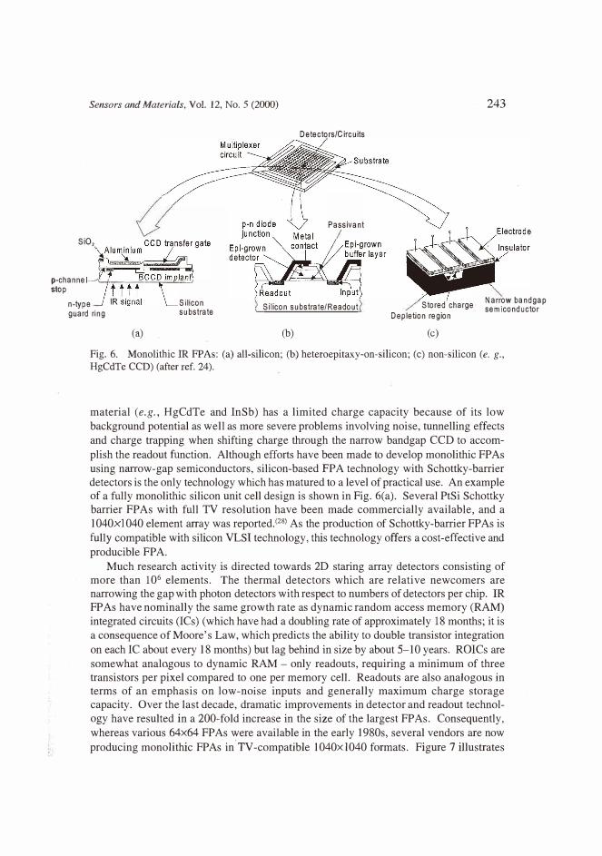
In the monolithic approach, some of the multiplexing is done in the detector material
itself rather than in an external readout circuit. The basic element of an monolithic an:ay
is a metal-insulator-semiconductor (MIS) structure as shown in Fig. 6(c). Used as part of a charge transfer device, a MIS capacitor detects and integrates the IR-generated photocurrent. Although most IR imaging applications tend to require high charge handling capabilities in the unit cells, an MIS capacitor fabricated in a narrow-gap semiconductor
Sensors and Materials, Vol. 12, No. 5 (2000) 243
Detectors/Circuits
Passivant
SiO,
p-channe 1�,-1--�=--=---=--,...::.:.cJc..c== stop
n-type guard ring
(a)
Silicon substrate
Silicon substrate/Readout
(b)
Stored charge
Depletion region
(c)
Narrow bandgap semiconductor
Fig. 6. Monolithic IR FPAs: (a) all-silicon; (h) heteroepitaxy-on-silicon; (c) non-silicon (e. g.,
HgCdTe CCD) (after ref. 24).
material (e.g., HgCdTe and InSb) has a limited charge capacity because of its low background potential as well as more severe problems involving noise, tunnelling effects and charge trapping when shifting charge through the narrow bandgap CCD to accomplish the readout function. Although efforts have been made to develop monolithic FP As using narrow-gap semiconductors, silicon-based FPA technology with Schottky-barrier detectors is the only technology which has matured to a level of practical use. An example of a fully monolithic silicon unit cell design is shown in Fig. 6(a). Several PtSi Schottky barrier FP As with full TV resolution have been made commercially available, and a 1040xl040 element array was reported.<28l As the production of Schottky-barrier FPAs is fully compatible with silicon VLSI technology, this technology offers a cost-effective and producible FP A.
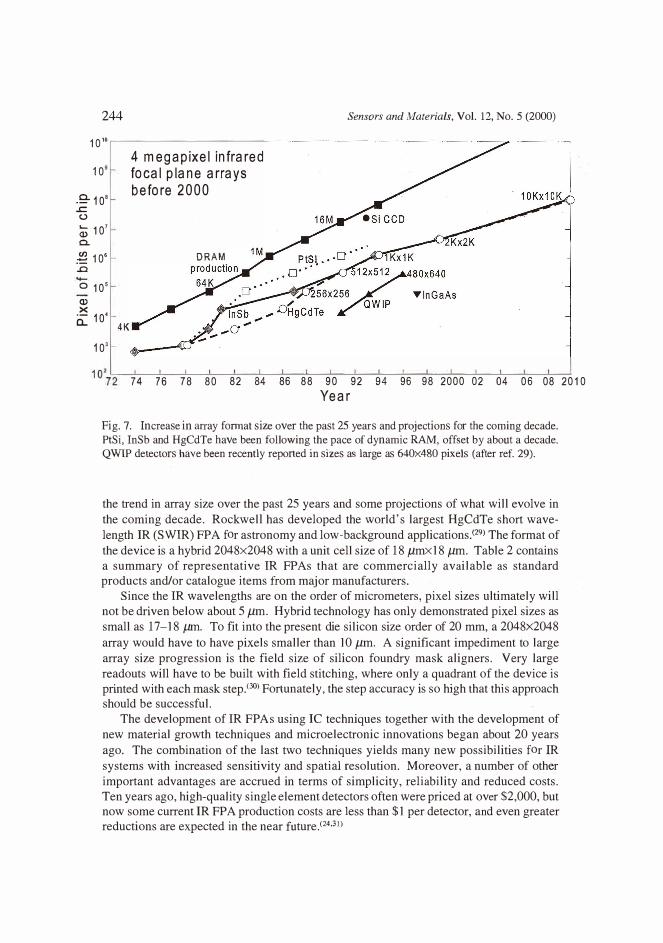
Much research activity is directed towards 2D staring array detectors consisting of more than 106 elements. The thermal detectors which are relative newcomers are narrowing the gap with photon detectors with respt!ct to numbers of detectors per chip. IR FP As have nominally the same growth rate as dynamic random access memory (RAM) integrated circuits (ICs) (which have had a doubling rate of approximately 18 months; it is a consequence of Moore's Law, which predicts the ability to double transistor integration on each IC about every 18 months) but lag behind in size by about 5-10 years. ROI Cs are somewhat analogous to dynamic RAM - only readouts, requiring a minimum of three transistors per pixel compared to one per memory cell. Readouts are also analogous in terms of an emphasis on low-noise inputs and generally maximum charge storage capacity. Over the last decade, dramatic improvements in detector and readout technology have resulted in a 200-fold increase in the size of the largest FPAs. Consequently, whereas various 64x64 FPAs were available in the early 1980s, several vendors are now producing monolithic FPAs in TV-compatible 1040xl040 formats. Figure 7 illustrates
244 Sensors and Materials, Vol. 12, No. 5 (2000)
10 10
1 0'
.9-10'
4 megapixel infrared focal plane arrays before 2000
..c:
(.)
� 10' 0..
� 10• DRAM
..a 0 105
Q) X
ii:: 1 0' 4K
103
74 76 78 80 82 84 86 88 90 92 Year
94 96 98 2000 02 04 06 08 2010
Fig. 7. Increase in array format size over the past 25 years and projections for the coming decade. PtSi, InSb and HgCdTe have been following the pace of dynamic RAM, offset by about a decade. QWIP detectors have been recently reported in sizes as large as 640x480 pixels (after ref. 29).
the trend in array size over the past 25 years and some projections of what will evolve in the coming decade. Rockwell has developed the world's largest HgCdTe short wavelength IR (SWIR) FPA for astronomy and low-background applications.<29
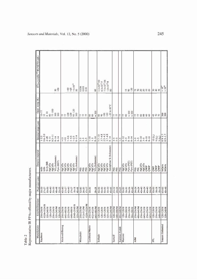
l The format of the device is a hybrid 2048x2048 with a unit cell size of 18 µmx18 µm. Table 2 contains a summary of representative IR FPAs that are commercially available as standard products and/or catalogue items from major manufacturers.
Since the IR wavelengths are on the order of micrometers, pixel sizes ultimately will not be driven below about 5 µm. Hybrid technology has only demonstrated pixel sizes as small as 17-18 µm. To fit into the present die silicon size order of 20 mm, a 2048x2048
array would have to have pixels smaller than 10 µm. A significant impediment to large array size progression is the field size of silicon foundry mask aligners. Very large readouts will have to be built with field stitching, where only a quadrant of the device is printed with each mask step.<30l Fortunately, the step accuracy is so high that this approach should be successful.
The development of IR FP As using IC techniques together with the development of new material growth techniques and microelectronic innovations began about 20 years
ago. The combination of the last two techniques yields many new possibilities for IR
systems with increased sensitivity and spatial resolution. Moreover, a number of other important advantages are accrued in terms of simplicity, reliability and reduced costs. Ten years ago, high-quality single element detectors often were priced at over $2,000, but now some current IR FPA production costs are less than $1 per detector, and even greater reductions are expected in the near future.<24•31l
Tab
le 2
Rep
rese
nta
tive
IR F
PA
s o
ffer
ed b
y m
ajo
r m
anufa
cture
rs.
Ma
nu
factu
rer
Size
/ Arc
hitec
ture
Pi
xel s
ize (u
m)
Dete
cto
r m
ate
rial
Rayt
heo
n 25
6x25
6/H
30
x30
lnSb
I 024
x I 02
4/H
27
x27
lnSb
32
0�24
0/H
50
x50
Si:A
s BIB
12
8xl2
8/H
40
x40
HgC
dTc
256x
2S6/
H
30x3
0 H
gCdT
e 32
0x24
0/M
48
x48
VO, (b
olom
eter)
32
8x24
5/H
35
x35
Pyro
(BST
) R
ockw
ell/B
oeing
25
6x25
6/H
40
x40
HgC
dTe
640x
480/
H
27x2
7 H
gCdT
e 22
5x25
6/H
40
x40
HgC
dTe
640x
480/
H
27x2
7 H
gCdT
e 20
48x2
048/
H
18xl
8 H
gCdT
e 32
0x24
0/M
48
x48
VO, (b
olom
eter)
M
itsu
bis
hi
256x
256/
M
52x4
0 Pt
Si
512x
512/
M
26x2
0 Pt
Si
I 024
x I 02
4/M
I 7
xl 7
PtSi
L
ockh
eed
Mar
tin
256x
256i
H
30x3
0 H
gCdT
e 43
2x43
2/H
H
gCdT
e 64
0x48
0/M
28
x28
VO
, (bol
omete
r)
Sofr
adir
128x
128/
H
50x5
0 H
gCdT
e 12
8xl2
8/H
50
x50
HgC
dTe
128x
128/
H
50x5
0 H
gCdT
e 32
0x24
0/H
30
x30
HgC
dTe
320x
240/
M
45x4
5 Am
orph
ous S
i (b
olom
eter
) Sa
rtlof
f 32
0x24
4/M
23
x32
PtSi
64
0x48
0/M
24
x24
PtSi
Ea
stman
-Kod
ak
486x
640/
M
25x2
5 Pt
Si
Marc
oni
128x
!28/
H
50x5
0 H
gCdT
e 38
4x28
8/H
30
x30
HgC
dTe
256x
!28/
H
56x5
6 Py
ro (P
Sn
384x
288/
H
40x4
0 Py
ro(P
ST)
AIM
25
6x25
6/M
24
x24
PtSi
48
6x64
0/M
24
x24
PtSi
25
6x25
6/H
40
x40
HgC
dTe
640x
512/
H
24x2
4 H
gCdT
e 25
6x25
6/H
40
x40
QW
IP
640x
512/
H
24x2
4 Q
WIP
JP
L
128x
l28/
H
50x5
0 Q
WP
256x
256/
H
38x3
8 Q
WIP
64
0x48
6/H
18
xl8
QW
IP
Sens
or.; U
nlim
ited
128x
l28/
H
60x6
0 ln
GaAs
32
0x24
0/H
40
x40
lnGa
As
Snec
tral r
anee
(um
) O
per.
tem
p. (K)
1-
5.5
10-7
7 0.
6-5.
0 35
2-28
4-
10
9-11
80
8.
5-11
77
-100
8-14
300
8-14
30
0 >1
5 77
>1
077
1-
4.6
120
1-4.
6 12
0 1-
2.5
95-1
208-
114
300
3-5
77
3-5
77
3-5
77
1-10
80
1--
5 80
8-
14
,.30
0 7.
7-10
80
3.
7-4.
8 90
2.
5-4.
2 19
5 3.
7-4.
8 12
0 8-
14
-20
to 60
°C
1-5
77
1-5
77
1-5
77
8-12
77
3-
580
8-
14
"30
0 8-
14
"30
0 3-
5 77
3-
5 77
8-
1080
3-
5 80
8-
10
60
8-10
60
15
(lc,)
45
9(
Ac)
70
9 (Ac
) 70
0.
9--1.
7 30
0 0.
9--1.
7 30
0
0•0,
.,) (c
mH
z112/W
)/NET
D (m
K)
50
>50
>IO
>2
5
>lx
l0
14
50
0.036
0.0
33
0.10
60
l.lx
1011
/10
4.3x
!011/7
7.Sx
!011
/36
1.0x
l012
/880 15
90
13
0 75
70
20
20
10
20
30
40
36
>
JO"
> 1
012
�
� S·
_1:,
<
?- ;;
z
!'.l
V,
246 Sensors and Materials, Vol. 12, No. 5 (2000)
Two generic types of silicon addressing circuits have been developed: CCDs and complementary metal-oxide-semiconductor (CMOS) switches. CCD technology is used for not very large scale arrays and their technology is more complicated than the CMOS. production line.
4.1 CCD and CMOS architectures
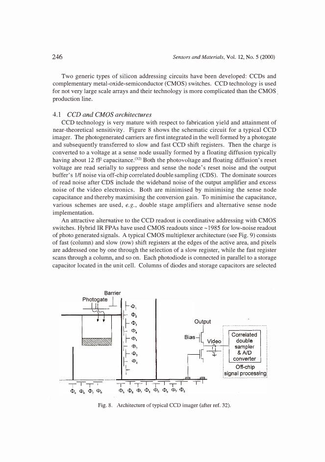
CCD technology is very mature with respect to fabrication yield and attainment of near-theoretical sensitivity. Figure 8 shows the schematic circuit for a typical CCD imager. The photogenerated carriers are first integrated in the well formed by a photogate and subsequently transferred to slow and fast CCD shift registers. Then the charge is converted to a voltage at a sense node usually formed by a floating diffusion typically having about 12 fF capacitance.c32l Both the photovoltage and floating diffusion's reset voltage are read serially to suppress and sense the node's reset noise and the output buffer's 1/f noise via off-chip correlated double sampling (CDS). The dominate sources of read noise after CDS include the wideband noise of the output amplifier and excess noise of the video electronics. Both are minimised by minimising the sense node capacitance and thereby maximising the conversion gain. To minimise the capacitance, various schemes are used, e.g., double stage amplifiers and alternative sense node implementation.
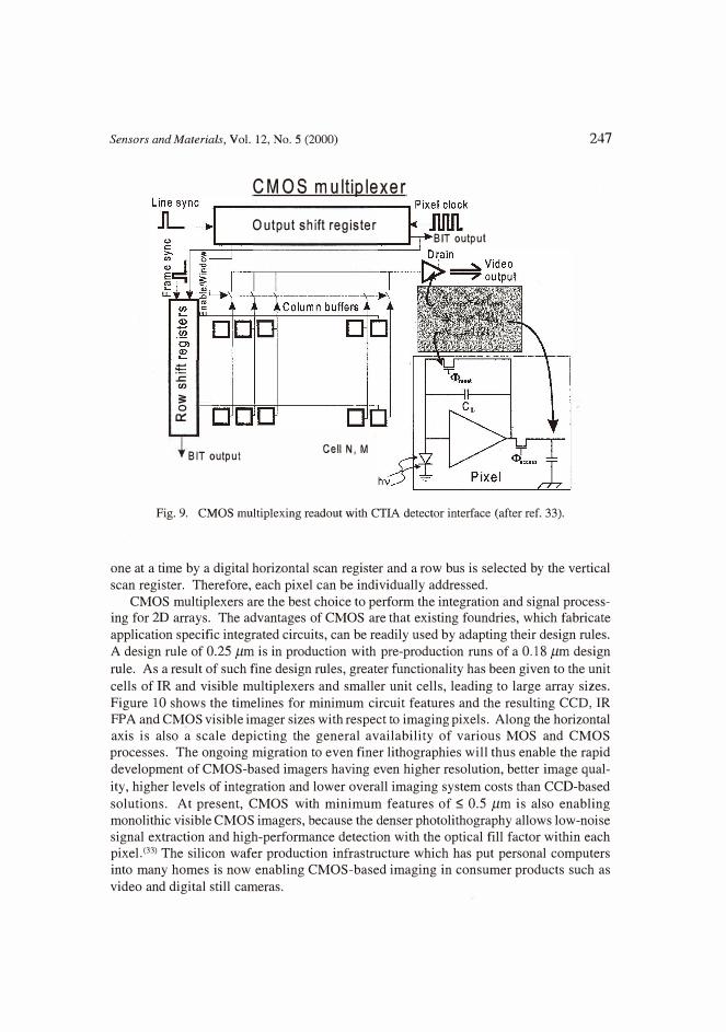
An attractive alternative to the CCD readout is coordinative addressing with CMOS switches. Hybrid IR FPAs have used CMOS readouts since -1985 for low-noise readout of photo generated signals. A typical CMOS multiplexer architecture (see Fig. 9) consists of fast (column) and slow (row) shift registers at the edges of the active area, and pixels are addressed one by one through the selection of a slow register, while the fast register scans through a column, and so on. Each photodiode is connected in parallel to a storage capacitor located in the unit cell. Columns of diodes and storage capacitors are selected
Barrier Photogate J_
Output
Fig. 8. Architecture of typical CCD imager (after ref. 32).
Sensors and Materials, Vol. 12, No. 5 (2000)
;; ..c:
rn
:;: 0 0:::
BIT output
CMOS multiplexer
Output shift register
Cell N, M
BIT output
Fig. 9. CMOS multiplexing readout with CTIA detector interface (after ref. 33).
247
one at a time by a digital horizontal scan register and a row bus is selected by the vertical
scan register. Therefore, each pixel can be individually addressed. CMOS multiplexers are the best choice to perform the integration and signal process
ing for 2D arrays. The advantages of CMOS are that existing foundries, which fabricate
application specific integrated circuits, can be readily used by adapting their design rules.
A design rule of 0.25 µm is in production with pre-production runs of a 0.18 µm design
rule. As a result of such fine design rules, greater functionality has been given to the unit
cells of IR and visible multiplexers and smaller unit cells, leading to large array sizes.
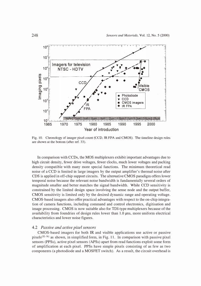
Figure 10 shows the timelines for minimum circuit features and the resulting CCD, IR FP A and CMOS visible imager sizes with respect to imaging pixels. Along the horizontal axis is also a scale depicting the general availability of various MOS and CMOS processes. The ongoing migration to even finer lithographies will thus enable the rapid
development of CMOS-based imagers having even higher resolution, better image qual
ity, higher levels of integration and lower overall imaging system costs than CCD-based
solutions. At present, CMOS with minimum features of s; 0.5 µm is also enabling monolithic visible CMOS imagers, because the denser photolithography allows low-noise signal extraction and high-performance detection with the optical fill factor within each pixel. <33l The silicon wafer production infrastructure which has put personal computersinto many homes is now enabling CMOS-based imaging in consumer products such as
video and digital still cameras.
248 Sensors and Materials, Vol. 12, No. 5 (2000)
1 O'
107
,,---------------�-------=�� .• .--, lmagers for television T T _,,_.,,- / 106
� 105
0.. Cl . E: 104
Cl C1' E
- 103
102
101 1965
NTSC - HDTV f ,,,,, .. 1.+T / I• / • 1•
:•
. : .........
/ / ..
J\T+
.: iVisible 'CMOS
1970
. / • •
/1R ;1/FPA
1975 1980 1985
• PhotodiodeT CCD• CMOS imagers+ IR FPA
1990 1995
Year of introduction
2000
Fig. 10. Chronology of imager pixel count (CCD, IR FP A and CMOS). The timeline design rules
are shown at the bottom (after ref. 33).
In comparison with CCDs, the MOS multiplexers exhibit important advantages due to high circuit density, fewer drive voltages, fewer clocks, much lower voltages and packing density compatible with many more special functions. The minimum theoretical read noise of a CCD is limited in large imagers by the output amplifier's thermal noise after CDS is applied in off-chip support circuits. The alternative CMOS paradigm offers lower temporal noise because the relevant noise bandwidth is fundamentally several orders of magnitude smaller and better matches the signal bandwidth. While CCD sensitivity is constrained by the limited design space involving the sense node and the output buffer, CMOS sensitivity is limited only by the desired dynamic range and operating voltage. CMOS-based imagers also offer practical advantages with respect to the on-chip integration of camera functions, including command and control electronics, digitisation and image processing. CMOS is now suitable also for TDI-type multiplexers because of the availability from foundries of design rules lower than 1.0 µm, more uniform electrical characteristics and lower noise figures.
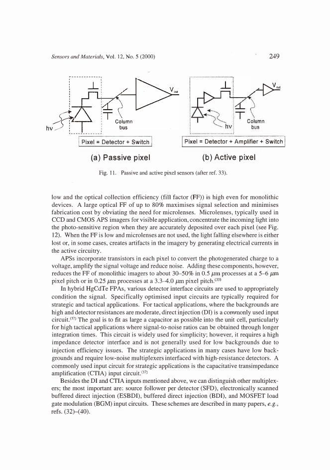
4.2 Passive and active pixel sensors CMOS-based imagers for both IR and visible applications use active or passive
pixels<32-35J as shown, in simplified form, in Fig. 11. In comparison with passive pixel
sensors (PPSs), active pixel sensors (APSs) apart from read functions exploit some form of amplification at each pixel. PPSs have simple pixels consisting of as few as two components (a photodiode and a MOSFET switch). As a result, the circuit overhead is
Sensors and Materials, Vol. 12, No. 5 (2000)
.-------------1 : ' ' '
·---
� hvj?
I------------ 1
I Pixel = Detector + Switch I
(a) Passive pixel
249
/� ....,_ __
L ____________________________ :
I Pixel = Detector+ Amplifier+ Switch I
(b) Active pixel
Fig. 11. Passive and active pixel sensors (after ref. 33).
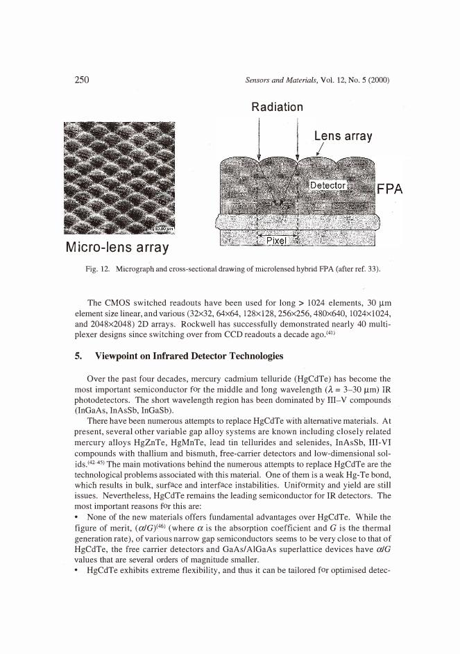
low and the optical collection efficiency (fill factor (FF)) is high even for monolithic devices. A large optical FF of up to 80% maximises signal selection and minimises fabrication cost by obviating the need for microlenses. Microlenses, typically used in CCD and CMOS APS imagers for visible application, concentrate the incoming light into the photo-sensitive region when they are accurately deposited over each pixel (see Fig. 12). When the FF is low and microlenses are not used, the light falling elsewhere is either lost or, in some cases, creates artifacts in the imagery by generating electrical currents in the active circuitry.
APSs incorporate transistors in each pixel to convert the photogenerated charge to a voltage, amplify the signal voltage and reduce noise. Adding these components, however, reduces the FF of monolithic imagers to about 30-50% in 0.5 µm processes at a 5-6 µm pixel pitch or in 0.25 µm processes at a 3.3-4.0 µm pixel pitch.<33l
In hybrid HgCdTe FPAs, various detector interface circuits are used to appropriately condition the signal. Specifically optimised input circuits are typically required for strategic and tactical applications. For tactical applications, where the backgrounds are high and detector resistances are moderate, direct injection (DI) is a commonly used input circuit.<37l The goal is to fit as large a capacitor as possible into the unit cell, particularly for high tactical applications where signal-to-noise ratios can be obtained through longer integration times. This circuit is widely used for simplicity; however, it requires a high impedance detector interface and is not generally used for low backgrounds due to injection efficiency issues. The strategic applications in many cases have low backgrounds and require low-noise multiplexers interfaced with high-resistance detectors. A commonly used input circuit for strategic applications is the capacitative transimpedance amplification (CTIA) input circuit.C37l
Besides the DI and CTIA inputs mentioned above, we can distinguish other multiplexers; the most important are: source follower per detector (SFD), electronically scanned buffered direct injection (ESBDI), buffered direct injection (BDI), and MOSFET load gate modulation (BGM) input circuits. These schemes are described in many papers, e.g.,
refs. (32)-(40).
250 Sensors and Materials, Vol. 12, No. 5 (2000)
Radiation
Lens array
I
Micro-lens array
Fig. 12. Micrograph and cross-sectional drawing ofmicrolensed hybrid FPA (after ref. 33).
The CMOS switched readouts have been used for long > 1024 elements, 30 µm element size linear, and various (32x32, 64x64, 128xl28, 256x256, 480x640, 1024x1024, and 2048x2048) 2D arrays. Rockwell has successfully demonstrated nearly 40 multiplexer designs since switching over from CCD readouts a decade ago.<41>
5. Viewpoint on Infrared Detector Technologies
Over the past four decades, mercury cadmium telluride (HgCdTe) has become the most important semiconductor for the middle and long wavelength (A= 3-30 µm) IR photodetectors. The short wavelength region has been dominated by III-V compounds (InGaAs, InAsSb, InGaSb).
There have been numerous attempts to replace HgCdTe with alternative materials. At present, several other variable gap alloy systems are known including closely related
mercury alloys HgZnTe, HgMnTe, lead tin tellurides and selenides, InAsSb, III-VI
compounds with thallium and bismuth, free-carrier detectors and low-dimensional solids.<42-45) The main motivations behind the numerous attempts to replace HgCdTe are the technological problems associated with this material. One of them is a weak Hg-Te bond, which results in bulk, surface and interface instabilities. Uniformity and yield are still issues. Nevertheless, HgCdTe remains the leading semiconductor for IR detectors. The most important reasons for this are:
None of the new materials offers fundamental advantages over HgCdTe. While the
figure of merit, (a/G)<46l (where a is the absorption coefficient and G is the thermalgeneration rate), of various narrow gap semiconductors seems to be very close to that of HgCdTe, the free carrier detectors and GaAs/AlGaAs superlattice devices have a/G values that are several orders of magnitude smaller.
HgCdTe exhibits extreme flexibility, and thus it can be tailored for optimised detec-
Sensors and Materials, Vol. 12, No. 5 (2000) 251
tion in any region of the IR spectrum, and dual and multicolour devices can be easily constructed.
The current development of IR photodetectors has been dominated by complex bandgap heterostructures. Among various variable band gap semiconductor alloys, HgCdTe is the only single material covering the whole IR spectral range having nearly the same lattice parameter. The difference in lattice parameter between Cd Te (E
g = 1.5 e Y) and
Hg0_8Cd0.2Te (Eg
= 0.1 eY) is"" 0.2%. Replacing a small fraction of Cd with Zn or Te with Se can compensate for the residual lattice mismatch. The independence of the lattice parameter from composition is a major advantage of HgCdTe over any other material.
Heterostructures do not offer any inherent fundamental advantages over homostructures for the conventional equilibrium mode devices. The fundamental limits to the performance of IR detectors are imposed by the unavoidable physics of optical and thermal generation in the narrow gap base region of a photodetector. Nevertheless, heterojunctions are helpful in achieving high performance in practice. For example, the narrow gap HgCdTe which absorbs infrared radiation can be buried encapsulated in wider gap
HgCdTe, thereby preventing instabilities due to the weak Hg-Te bonds. In addition, heterostructures can be used for nonequilibrium devices for which the potential performance is much higher than that of conventional ones.<47>
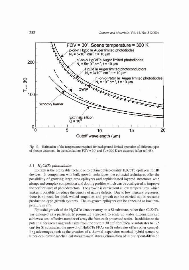
When background-photon noise is the dominant noise mechanism, the detector is operating in an ideal mode and is said to exhibit background limited performance (BLIP). The BLIP temperature is defined as the temperature at which the device operates when the dark current equals the background photocurrent for a given field of view (FOY) and a
background temperature. In Fig. 13, plots of the calculated temperature required for BLIP operation in 30° FOY are shown as a function of cutoff wavelength. We can see that the operating temperature of "bulk" intrinsic IR detectors (HgCdTe and PbSnTe) is higher than for other types of photon detectors. HgCdTe detectors with background limited performance operate with thermoelectric coolers in the MWIR range, but the L WIR detectors (8 $ Ac $ 12 µm) operate at"" 100 K. HgCdTe photodiodes exhibit higher operating temperatures than extrinsic detectors, silicide Schottky barriers and quantum
well infrared photodetectors (QWIPs). However, the cooling requirements for QWIPs
with cutoff wavelengths below 10 µm are less stringent in comparison with extrinsic detectors and Schottky barrier devices.
Recently, more interest has been focused on p-n junction photodiodes. Photodiodes with very low power dissipation, easy multiplexing on focal plane silicon chips and less stringent noise requirements for the readout devices and circuits can be assembled in 2D arrays containing a very large (� 106) number of elements, limited only by existing
technologies. Photodiodes can also have less low-frequency noise, faster response time, and the potential for a more uniform spatial response across each element. However, the more complex processes needed for photovoltaic detectors have caused slower development and industrialisation of the second generation systems, particularly for very large arrays.
Photovoltaic HgCdTe FP As are based on p-type and n-type materials. Linear (240,
288, 480, and 960 elements), 2D scanning arrays with TDI, and 2D staring formats from 32x32 up to 2048x2048 have been made. Pixel sizes ranging from 18 µm square to over 1 mm have been demonstrated. The best results have been obtained using hybrid architectures and exploiting advances in CMOS fabrication processes.
-
0..
:::; m
252
200
Sensors and Materials, Vol. 12, No. 5 (2000)
FOV = 30°
, Scene temperature= 300 K p-on-n HgCdTe Auger limited photodiodesN
d= 5x1014 cm-a, t = 10 µm
n'-on-p H�CdTe Auger limited photodiodesN. = 5x10 5 cm-3, t = 10 µm
HgCdTe Auger limited photoconductors Nd
= 3x1014 cm-a, t = 10 µm n'-on-p PbSnTe Auger limited photodiodes N. = 1011 cm-a, t = 10 µm
100
Schottky barrier
5
Extrinsic silicon Q = 1010
10
Cutoff wavelength (µm)
15
Fig. 13. Estimation of the temperature required for background limited operation of different types of photon detectors. In the calculations FOV = 30° and T8 = 300 Kare assumed (after ref. 48).
5.1 HgCdTe photodiodes
Epitaxy is the preferable technique to obtain device-quality HgCdTe epilayers for IR
devices. In comparison with bulk growth techniques, the epitaxial techniques offer the
possibility of growing large area epilayers and sophisticated layered structures with
abrupt and complex composition and doping profiles which can be configured to improve
the performance of photodetectors. The growth is carried out at low temperatures, which
makes it possible to reduce the density of native defects. Due to low mercury pressures, there is no need for thick-walled ampoules and growth can be carried out in reusable production-type growth systems. The as-grown epilayers can be annealed at low temperature in situ.
Epitaxial growth of the HgCdTe detector array on a Si substrate, rather than CdZnTe,
has emerged as a particularly promising approach to scale up wafer dimensions and
achieve a cost-effective number of array die from each processed wafer. In addition to the
potential for increasing wafer size from the current 30 cm2 for CdZnTe substrates to 125
cm2 for Si substrates, the growth of HgCdTe FP As on Si substrates offers other compelling advantages such as the creation of a thermal-expansion matched hybrid structure,
superior substrate mechanical strength and flatness, elimination of impurity out-diffusion
20
Sensors and Materials, Vol. 12, No. 5 (2000) 253
from the substrate, and compatibility with automated wafer processing and handling
methodologies.
Among the various epitaxial techniques, liquid phase epitaxy (LPE) is the most mature method. LPE growth must be carried out at a relatively high growth temperature with adherent interdiffusion and the resulting graded interfaces. Recent efforts are aimed mostly at low-growth-temperature techniques: metalorganic chemical vapour deposition
(MOCVD) and molecular beam epitaxy (MBE). MOCVD is a nonequilibrium method
that appears to be most promising for the future large-scale and low-cost production of
epilayers. The important advantage of this method is reduced growth temperature and the
ability to modify the conditions during growth to obtain the required band gap and doping profiles.
Intensive studies are currently underway on MBE. This technique offers unique capabilities in material and device engineering, including the lowest growth temperature, superlattice growth and potential for the most sophisticated composition and doping
profiles. The growth temperature is less than 200 °C for MBE but around 350 °C for
MOCVD, making it more difficult to control the p-type doping in MOCVD due to the
formation of Hg vacancies at higher growth temperatures. The main drawback of both technologies is the high cost of equipment and maintenance. This has prevented the more widespread use of these methods.
Up to now, the realisation of HgCdTe photodiodes has usually been based on the most common n+-p and 1i+-n structure (symbol"+" denotes strong doping, underlined "_"
denotes a wider gap). In such diodes, the lightly doped narrow-gap absorbing region
("base" of the photodiode) determines the dark current and photocurrent. In these
photodiodes the base p-type layers (or n-type layers) are sandwiched between CdZnTe substrate and high-doped (in n+-p structures) or wider-gap (in 12+-n structure) regions. Due to back side illumination (through the CdZnTe substrate) and internal electric fields (which are "blocking" for minority carriers), the influence of surface recombinations on photodiode performance is eliminated. The influence of surface recombination can also
be prevented by suitable passivation. Both optical and thermal generation is suppressed in
the n+-region due to the Burstein-Moss effect and in the 12+-region due to wide gap. Thus
the Rc/4 product of the double-layer heterojunction (DLHJ) structure is higher than that of
the homostructure. The thickness of the base region should be optimised for near unity quantum effi
ciency and low dark current. This is achieved with a base thickness slightly higher than the inverse absorption coefficient for single pass devices: t = 1/a (which is sslO µm) or
half of the 1/a for double pass devices (devices supplied with a retroreflector). Low
doping is beneficial for low thermal generation and high quantum efficiency.
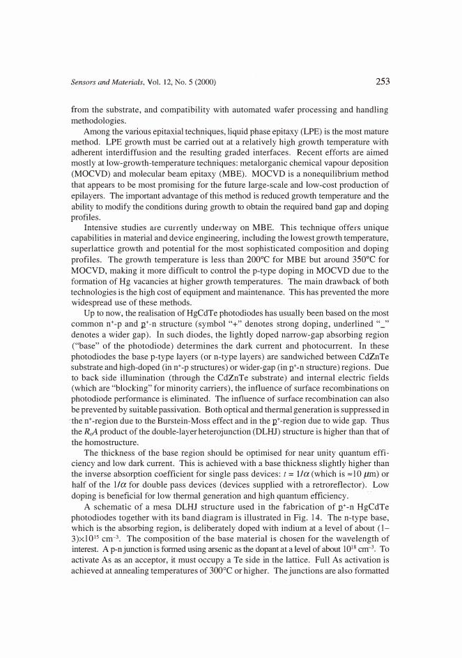
A schematic of a mesa DLHJ structure used in the fabrication of g+-n HgCdTe photodiodes together with its band diagram is illustrated in Fig. 14. The n-type base, which is the absorbing region, is deliberately doped with indium at a level of about ( l-3 )xl0 15 cm-3. The composition of the base material is chosen for the wavelength ofinterest. A p-njunction is formed using arsenic as the dopant at a level of about 10 18 cm- 3
• To
activate As as an acceptor, it must occupy a Te side in the lattice. Full As activation is
achieved at annealing temperatures of 300 °C or higher. The junctions are also formatted
(a)
(b)
254 Sensors and Materials, Vol. 12, No. 5 (2000)
Au contact
CdT (p ssi ation)
Arsenic-doped (p-type) n-type cap x,
n-type base x, x,> x,
CdZnTe substrate
E,
x<y
CdZnTe ---•t•----n-type Hg1_xCdxTe ---.14-:----.i
substrate base layer t Q-type Hg
1_YCd
yTe
cap layer
Fig. 14. DLHJ mesa p,+-n HgCdTe photodiode: (a) schematic cross-sectional view; (b) band
diagram.
by As selective implantation through windows made on a mask of photoresisUZnS and then diffusion of the arsenic through the cap layer into the narrow-gap base layer. After implantation, the sample underwent two consecutive annealings, one at about 430°C (to diffuse the arsenic into the base layer) for approximately 10 min and the other at 250°C (to annihilate Hg vacancies formed in the HgCdTe lattice during the growth and diffusion of
Sensors and Materials, Vol. 12, No. 5 (2000) 255
arsenic). C49l The p-type capping layers with composition y > x have a thickness of 1-2 µm.
The electrical junction is positioned near the metallurgical interface, and it is wise to place the junction in the small band-gap layer to avoid deleterious effects on the quantum efficiency and dark currents. At present, most laboratories are using CdTe or CdZnTe (deposited by MBE, MOCVD, sputtering and e-beam evaporation) for photodiode passivation. <49l
Rogalski and Ciupa have compared the performance of n+-p and Q+�n LWIR HgCdTe photodiodes.csoJ It appears that, for the lowest doping levels achievable in a controllable manner in the base regions of photodiodes (Na
= 5xl0 15 cm- 3 for n+-p structure, and Nct =
5xl 0 14 cm- 3 for Q+-n structure), the performance of both types of photodiodes is comparable for a given cutoff wavelength and temperature.
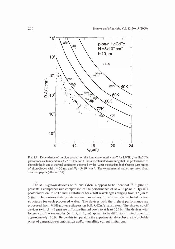
5.1.1 L WIR photodiodes The dependence of the base region diffusion limited RoA product on the long wave
length cutoff for p+ -on-n L WIR HgCdTe photodiodes at different temperatures is shown in Fig. 15. This figure also includes the experimental data reported by many authors for DLHJ p-on-n structures. The wider bandgap cap layer contributes a negligible amount of thermally generated diffusion current, compared with that from an n-type absorber layer at 77 K, and the higher values of experimental data are situated about half of an order of magnitude below ultimate theoretical predictions. With a lowering of the operating temperature of photodiodes, the discrepancy between the theoretical curves and experimental data increases due to additional currents in the junctions (such as tunnelling current or surface leakage current) that are not considered. Photodiodes with lower performance usually contain metallurgical defects such as dislocation clusters and loops, pin holes, striations, Te inclusions and heavy terracing. Diodes with the highest performance at 40 K contain no visible defects (Hg interstitials and vacancies). However, it should be noted that the higher values of experimental data in the very long wavelength range (above 14 µm) at lower temperatures (40 K) coincide very well with theoretical predictions. The best devices continued to be diffusion-current limited by the Auger mechanism at zero bias to 35 K. At 40 K; the measured Rc,A is 2xl04 Qcm2 and the measured cutoff wavelength is 17 .6 µm. At 35 K, Rc,A is 2x10⁵ Qcm2 at a cutoff wavelength of 18.1 µm. The performance of photodiodes with cutoff wavelengths of 20.3 µm at 40 K is diffusion limited, and Rc,A products for the diodes reach values in the 103
Qcm2 range. These are the highest reported values at long cutoffs wavelengths for any HgCdTe device.
5. 1.2 MWIR photodiodesMiddle wavelength infrared HgCdTe photodiodes were the first to be developed, and
many mature technologies have been used to demonstrate FPAs.<52·53
l Since 1989 , the Santa Barbara Research Center (SBRC) has successfully utilised "infinite-melt" vertical LPE technology from Hg-rich solutions to grow high-quality epitaxial HgCdTe on the Sibased alternative substrates for the fabrication of p-on-n DLHJ detectors for highperformance MWIR FPAs. Tung et al. c54
l reported large MWIR FPAs, up to 480x640 pixels, grown on Si-based alternative substrates.
256
106
104
10°
8
.
0 • .
� 0. +
•
•o
. .
t:.. .o.: + •
x"
12
+
Sensors and Materials, Vol. 12, No. 5 (2000)
p-on-n HgCdTe
Nd=5x10
14
cm-3
t=10µm
16 A
c(µm)
•(351<)
20 24
Fig. 15. Dependence of the R,,A product on the long wavelength cutoff for LWIR 12+-n HgCdTe
photodiodes at temperatures � 77 K. The solid lines are calculated assuming that the performance of
photodiodes is due to thermal generation governed by the Auger mechanism in the base n-type region
of photodiodes with t = 10 µm and Nct = 5xl014 cm-3• The experimental values are taken from
different papers (after ref. 51).
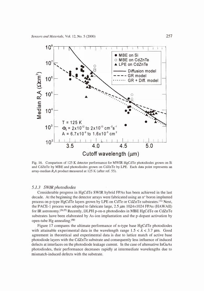
•'
The MBE-grown devices on Si and CdZnTe appear to be identica1.<55l Figure 16 presents a comprehensive comparison of the performance of MWIR 1t-on-n HgCdTe photodiodes on CdZnTe and Si substrates for cutoff wavelengths ranging from 3.5 µm to
5 µm. The various data points are median values for mini-arrays included in-test structures for each processed wafer. The devices with the highest performance are processed from MBE-grown epilayers on bulk CdZnTe substrates. The shorter cutoff devices (with,\"" 3 µm) are diffusion-limited down to at least 125 K. The devices with longer cutoff wavelengths (with Ac
"" 5 µm) appear to be diffusion-limited down to approximately 110 K. Below this temperature the experimental data obscure the probable onset of generation-recombination and/or tunnelling current limitations.
Sensors and Materials, Vol. 12, No. 5 (2000)
107
103
' ... 0 ' • ... 8 ' .. 'I,, •4.. • ', .... 1*. ..
·'l�,..,.
-�� ....... · . ...
• MBE on Si
o M BE on Cd Zn Te
• LPE on CdZnTe
--- Diffusion model
----GR model
· · · · · · · GR+ Diff. model
· . ..... . -:- ...
... •o
0
T = 125 K
<l>b = 2x10¹²
to 2x1013 cm·2s·1
A= 6.7x10·6
to 1.6x10·5 cm 2
·· .. .......
• •
257
102L.......L_____J,__J_,--'-----'--'------'----__J__-'----'-----'--'---"--'--"-'--------L----'------'-----'-"-'
3.5 4.0 4.5 5.0
Cutoff.wavelength (µm)
Fig. 16. Comparison of 125 K detector performance for MWIR HgCdTe photodiodes grown on Si
and CdZnTe by MBE and photodiodes grown on CdZnTe by LPE. Each data point represents an
array-median R,,A product measured at 125 K (after ref. 55).
5.1.3 SWIR photodiodes Considerable progress in HgCdTe SWIR hybrid FPAs has been achieved in the last
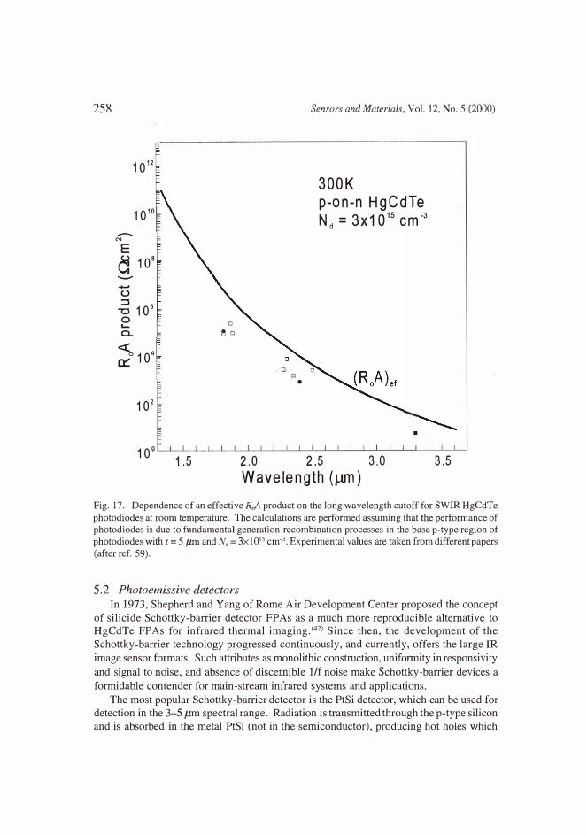
decade. At the beginning the detector arrays were fabricated using an n+ boron implanted process on p-type HgCdTe layers grown by LPE on CdTe or CdZnTe substrates.c52l Next, the PACE-I process was adopted to fabricate large, 2.5 µm 1024x1024 FPAs (HAWAII) for IR astronomy.<56·57l Recently, DLPH p-on-n photodiodes in MBE HgCdTe on CdZnTe substrates have been elaborated by As-ion implantation and the p-dopant activation by open-tube Hg annealing.<58l
Figure 17 compares the ultimate performance of n-type base HgCdTe photodiodes with attainable experimental data in the wavelength range 1.5 <A< 3.7 µm. Good agreement in theoretical and experimental data is due to lattice match of active base photodiode layers with the CdZnTe substrate and consequently less influence of induced defects at interfaces on the photodiode leakage current. · In the case of alternative InGaAs photodiodes, their performance decreases rapidly at intermediate wavelengths due to mismatch-induced defects with the substrate.
258 Sensors and Materials, Vol. 12, No. 5 (2000)
1012
300K
1010p-on-n HgCdTeN = 3x10 15 cm·3
d
--
N
E
a 108
-
......
(.)
:::,
"'C
106
D ,_ c.. � D
<(
0::.0
104
D •
102
•
10°
1.5 2.0 2.5 3.0 3.5
Wavelength (µrn)
Fig. 17. Dependence of an effective Rc,A product on the long wavelength cutoff for SWIR HgCdTe
photodiodes at room temperature. The calculations are performed assuming that the performance of photodiodes is due to fundamental generation-recombination processes in the base p-type region of photodiodes with t = 5 µm andN, = 3xl0 15 cm·3• Experimental values are taken from different papers(after ref. 59).
5.2 Photoemissive detectors
In 1973, Shepherd and Yang of Rome Air Development Center proposed the concept of silicide Schottky-barrier detector FP As as a much more reproducible alternative to HgCdTe FPAs for infrared thermal imaging.<42) Since then, the development of theSchottky-barrier technology progressed continuously, and currently, offers the large IR
image sensor formats. Such attributes as monolithic construction, uniformity in responsivity
and signal to noise, and absence of discernible 1/f noise make Schottky-barrier devices a
formidable contender for main-stream infrared systems and applications.
The most popular Schottky-barrier detector is the PtSi detector, which can be used for detection in the 3-5 µm spectral range. Radiation is transmitted through the p-type silicon and is absorbed in the metal PtSi (not in the semiconductor), producing hot holes which
Sensors and Materials, Vol. 12, No. 5 (2000) 259
are then emitted over the potential barrier into the silicon, leaving the silicide negatively charged. This fundamental difference in the detection mechanism underlies the unique properties of Schottky sensors, including their exceptional spatial uniformity and their modified Fowler spectral response. The negative charge of the silicide is transferred to a CCD by the direct charge injection method.
The fundamental source of dark current in the devices is the thermionic emission of holes over the potential barrier. Schottky photoemission is independent of such factors as semiconductor doping, minority carrier lifetime and alloy composition, and, as a result, has spatial uniformity characteristics that are far superior to those of other detector technologies. Uniformity is only limited by the geometric definition of the detectors. The effective quantum efficiency in the 3-5 µm atmospheric window is very low, on the order of 1 %, but useful sensitivity is obtained by near full frame integration in area arrays.
The Schottky-barrier detector is typically operated in the back side illumination mode. The quantum efficiency has been improved by thinning the PtSi film. The thinning is effective down to the PtSi thickness of 2 nm.<60> Another means of improving responsivity
is the implementation of an "optical cavity." The optical cavity structure consists of the metal reflector, the dielectric film between the reflector and the metal electrode of the Schottky-barrier diode (see Fig. 18). According to fundamental optical theory, the effect of the optical cavity depends on the thickness and refractive index of the dielectric films and on the wavelength. The conventional 1/4 wavelength design for optical cavity thickness is a good first approximation for optimising the responsivity.
Progress in Schottky-barrier FPA technology has been constant. At the present time,
Schottky-barrier FPAs represent the most advanced technology in FP As for many short wavelength (1 to 3 µm) and medium wavelength (3 to 5 µm) applications. Scanning PtSi FPAs with up to 4x4096 elements<61> and 2048x16 TDJ<62l elements were developed for space-borne remote sensing applications. A partial list of demonstrated configurations include square formats of 128x128, 256x256, 512x512, and 1040x1040, and rectangular formats of 244x320,280x340,244x512,234x487,512x488,488x512,648x487,480x640, 811x508, and 801x512. Reviews of different configuration of Schottky-barrier FPAs
have been published, e.g., by Kosonocky,<60l Kimata and Tsubouchi,<63> and Kimata et
a[.(64)
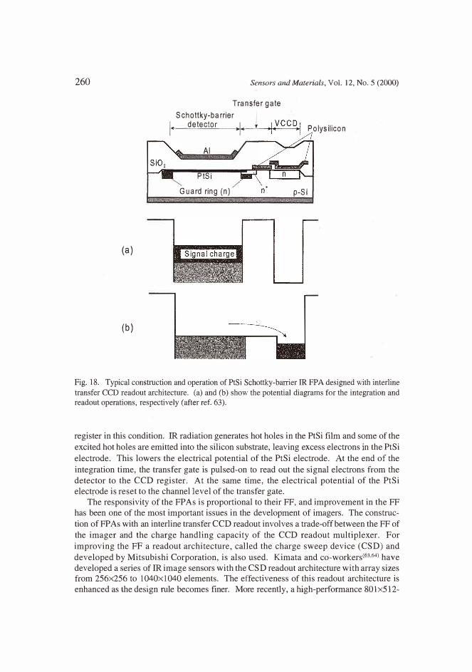
The details of the geometry and the method of charge transfer differ for different manufacturers. The design of staring Schottky-barrier FPAs for given pixel sizes and design rules involves a trade-off between the charge handling capacity and the FF. Most of the reported Schottky-barrier FPAs have the interline transfer CCD architecture. A typical cross-sectional view of the pixel and its operation in interline transfer CCD
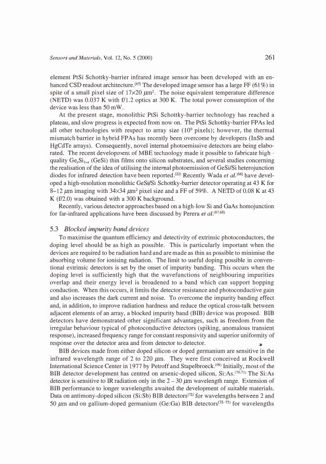
architecture is shown in Fig. 18. The pixel consists of a Schottky-barrier detector with an optical cavity, a transfer gate and a stage of vertical CCD. The n-type guard ring on the periphery of the Schottky-barrier diode reduces the edge electric field and suppresses the dark current. The effective detector area is determined by the inner edge of the guard ring. The transfer gate is an enhancement MOS transistor. The connection between the detector and the transfer gate is made by an n+ diffusion. A buried-channel CCD is used for the vertical transfer. During the optical integration time the surface-channel transfer gate is biased into accumulation. The Schottky-barrier detector is isolated from the CCD
260
(a)
(b)
Sensors arid Materials, Vol. 12, No. 5 (2000)
Transfer gate Schottky-barrier l
I, detector +
Al
PtSi Guard ring (n)
Polysilicon
p-Si
Fig. 18. Typical construction and operation of PtSi Schottky-barrier IR FPA designed with interline
transfer CCD readout architecture. (a) and (b) show the potential diagrams for the integration and readout operations, respectively (after ref. 63).
register in this condition. IR radiation generates hot holes in the PtSi film and some of the excited hot holes are emitted into the silicon substrate, leaving excess electrons in the PtSi electrode. This lowers the electrical potential of the PtSi electrode. At the end of the integration time, the transfer gate is pulsed-on to read out the signal electrons from the detector to the CCD register. At the same time, the electrical potential of the PtSi electrode is reset to the channel level of the transfer gate.
The responsi vity of the FP As is proportional to their FF, and improvement in the FF has been one of the most important issues in the development of imagers. The construction of FP .As with an interline transfer CCD readout involves a trade-off between the FF of the imager and the charge handling capacity of the CCD readout multiplexer. For improving the FF a readout architecture, called the charge sweep device (CSD) and developed by Mitsubishi Corporation, is also used. Kimata and co-workersC63·64l have developed a series cif IR image sensors with the CSD readout architecture with array sizes from 256x256 to 1040x1040 elements. The effectiveness of this readout architecture is enhanced as the design rule becomes finer. More recently, a high-performance 801x512-
Sensors and Materials, Vol. 12, No. 5 (2000) 261
element PtSi Schottky-barrier infrared image sensor has been developed with an enhanced CSD readout architecture. <65> The developed image sensor has a large FF ( 61 % ) in spite of a small pixel size of 17x20 µm2
• The noise equivalent temperature difference (NETD) was 0.037 K with f/1.2 optics at 300 K. The total power consumption of thedevice was less than 50 mW.
At the present stage, monolithic PtSi Schottky-barrier technology has reached a plateau, and slow progress is expected from now on. The PtSi Schottky-barrier FPAs led all other technologies with respect to array size (106 pixels); however, the thermal mismatch barrier in hybrid FPAs has recently been overcome by developers (InSb and HgCdTe arrays). Consequently, novel internal photoemissive detectors are being elaborated. The recent development of MBE technology made it possible to fabricate high -quality GexSi 1_x (GeSi) thin films onto silicon substrates, and several studies concerning the realisation of the idea of utilising the internal photoemission of GeSi/Si heterojunction diodes for infrared detection have been reported.c22l Recently Wada et al.<66l have developed a high-resolution monolithic GeSi/Si Schottky-barrier detector operating at 43 K for 8-12 µm imaging with 34x34 µm2 pixel size and a FF of 59%. A NETD of 0.08 K at 43K (f/2.0) was obtained with a 300 K background.
Recently, various detector approaches based on a high-low Si and GaAs homojunction for far-infrared applications have been discussed by Perera et al.<67•68>
5.3 Blocked impurity band devices
To maximise the quantum efficiency and detectivity of extrinsic photoconductors, the doping level should be as high as possible. This is particularly important when the devices are required to be radiation hard and are made as thin as possible to minimise the absorbing volume for ionising radiation. The limit to useful doping possible in conventional extrinsic detectors is set by the onset of impurity banding. This occurs when the doping level is sufficiently high that the wavefunctions of neighbouring impurities overlap and their energy level is broadened to a band which can support hopping conduction. When this occurs, it limits the detector resistance and photoconductive gain and also increases the dark current and noise. To overcome the impurity banding effect and, in addition, to improve radiation hardness and reduce the optical cross-talk between adjacent elements of an array, a blocked impurity band (BIB) device was proposed. BIB detectors have demonstrated other significant advantages, such as freedom from the irregular behaviour typical of photoconductive detectors (spiking, anomalous transient response), increased frequency range for constant responsivity and superior uniformity of response over the detector area and from detector to detector. �
BIB devices made from either doped silicon or doped germanium are sensitive in the infrared wavelength range of 2 to 220 µm. They were first conceived at Rockwell International Science Center in 1977 by Petroff and Stapelbroeck.<69> Initially, most of the BIB detector development has centred on arsenic-doped silicon, Si:As_(7o,7i
J The Si:As detector is sensitive to IR radiation only in the 2- 30 µm wavelength range. Extension of BIB performance to longer wavelengths awaited the development of suitable materials. Data on antimony-doped silicon (Si:Sb) BIB detectors<72l for wavelengths between 2 and 50 µm and on gallium-doped germanium (Ge:Ga) BIB detectors(73
-75J for wavelengths
262 Sensors and Materials, Vol. 12, No. 5 (2000)
between 50 and 220 µm have been published. For a detailed analysis of the BIB detector see Szmulowicz and Madarsz.<76J
Impressive progress has been achieved in Si BIB array technology over the last decade. BIB devices in large staring array formats are now becoming commercially available. They open the possibility for astronomers to efficiently observe in the VL WIR spectral range, where at high altitudes the atmosphere has reasonable transmission. The best results have been achieved to date for Si:As BIB hybrid FPAs produced by Hughes Technology Center in Carlsbad07,7sJ and Rockwell International Science Center in Anaheim. <79J
Hybrid FPAs with Si:As BIB detectors operating in the 4-1 OK temperature range have been optimised for low, moderate and high IR backgrounds. The 256x256 format with 30 µm pixels and 240x320 format with 50 µm pixels are available for low- and highbackground applications, respectively. Antimony-doped silicon (Si:Sb) arrays and 128x128 pixel Si:Sb HFPAs having response to wavelengths> 40 µm have also been demonstrated, primarily for use at low and moderate backgrounds. Germanium BIB devices have been developed on an experimental basis, but they have not been reported in large 2D array formats yet.
5.4 InSb photodiodes InSb material is far more mature than HgCdTe and high-quality bulk substrates more
than 5 cm in diameter are commercially available. Fabrication techniques for InSb photodiodes use gaseous diffusion, and a subsequent etch results in a p-type mesa on ntype substrate with a donor concentration of about 1015 cm- 3
, A highly controlled diffusion process allows p-layer diffusion to occur with little surface damage, eliminating the need for deep diffusion and subsequent etch-back. This permits total mesa heights of only a few microns. A grounded "buried-metallization" proces�, independent of bondpad metallization, was developed to render the surface of InSb opaque, with the exception of the active area and the contact area. The accuracy of the photolithography along with the controlled diffusion process provide excellent uniformity of response.
InSb photodiodes operating at 3-5 µm are widely used for ground-based infrared astronomy and for applications aboard the Space Infrared Telescope Facility (SIRTF). For applications in astrophysics, these devices are very often operated at 4-7 K with a resistive or capacitive transimpedance amplifier to achieve the lowest noise petformance. InSb photodiodes can also be operated in the temperature range above 77 K. Of course, the RA products degrade in this region. At 120 K, RA products of 104 Qcm2 are still achieved with a slight reverse bias, making BLIP operation possible. The quantum efficiency in InSb photodiodes optimised for this temperature range remains unaffected up to 160 K.
InSb devices are usually made with both p-n junction and MIS capacitors. To maximise the available resolution and response of photodiodes, the bulk material is thinned to about 10 µm.<80l Staring arrays of back-side-illuminated, direct hybrid InSb detectors in 58x62, 64x64, 128x128, 200x200, 256x256, and 640x480C22J formats are available with readouts suitable for both high-background f/2 operation and for lowbackground astronomy applications. Linear array formats of 64, 128 and 256 elements
Sensors and Materials, Vol. 12, No. 5 (2000) 263
are also produced with front-side-illuminated detectors for both high-background and astronomy applications. Element sizes depend on device format and range from 20x20 to 200x200 µm. The U.S. Naval Observatory and the National Optical Astronomy Observatories in collaboration with the SBRC developed a 1024xl024 InSb FPA.(SJJ The architecture of this device consists of four independent 512x512 quadrants with eight outputs per quadrant.
The cryogenically cooled InSb and HgCdTe arrays have comparable array sizes and pixel yield in the MWIR spectral band. However, wavelength tunability and high
quantum efficiency have made HgCdTe the preferred material.
5.5 GaAs/AlGaAs QWJPs
Among the different types of QWIPs, the technology of the GaAs/ AlGaAs multiple quantum well detectors is the most mature. Rapid progress has been recently made in the performance of these detectors. Detectivities have improved dramatically, and are now
high enough so that large 640x480 FPAs with L WIR imaging performance comparable to
state-of-the-art HgCdTe are fabricated.<82-84l
QWIP technology is based on the well-developed A3B5 material system which has a large industrial base with a number of military and commercial applications. QWIPs cannot compete with HgCdTe photodiodes as the single device especially at higher operating temperatures (> 70 K), due to fundamental limitations associated with intersubband transitions.<85•86l However, the advantage of HgCdTe is less distinct in thetemperature range below 59 K due to problems associated with the HgCdTe material (p
type doping, Shockley-Read recombination, trap-assisted tunnelling, surface and interface instabilities). Even though a QWIP is a photoconductor, several of its properties such as high impedance, fast response time, long integration time, and low power consumption, comply well with the requirements of the fabrication of large FP As. Due to the high material quality at low temperature, QWIP has potential advantages over HgCdTe for VLWIR FPA applications in terms of the array size, uniformity, yield and cost of the systems.
All QWIPs are based on the "bandgap engineering" of layered structures of wide bandgap (relative to thermal IR energies) materials. The structure is designed so that the energy separation between two of the states in the structure matches the energy of the infrared photons to be detected. Several QWIP configurations have been reported based on transitions from bound-to-extended states, bound-to-quasicontinuum states, bound-toquasibound states, and bound-to-miniband states.
Figure 19 shows two detector configurations used in the fabrication of QWIP FPAs.
The major advantage of the bound-to-continuum QWIP is that the photoelectron can escape from the quantum well to the continuum transport states without being required to tunnel through the barrier. As a result, the voltage bias required to efficiently collect the photoelectrons can be reduced dramatically, thereby lowering the dark current. Furthermore, since the photoelectrons do not have to tunnel through them, the AlGaAs barriers can be made thicker without reducing the photoelectron collection efficiency. It appears that the dark current decreases significantly when the first excited state is dropped from
the continuum to the well top (see Fig. 20), bound-to-quasibound QWIP, without sacrificing the responsivity.
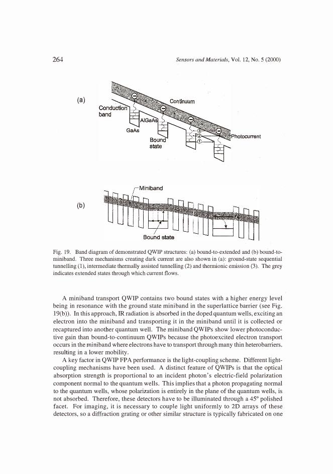
264 Sensors and Materials, Vol. 12, No. 5 (2000)
(a)
Photocurrent
(b)
Fig. 19. Band diagram of demonstrated QWIP structures: (a) bound-to-extended and (b) bound-tominiband. Three mechanisms creating dark current are also shown in (a): ground-state sequential tunnelling (1), intermediate thermally assisted tunnelling (2) and thermionic emission (3). The grey indicates extended states through which current flows.
A miniband transport QWIP contains two bound states with a higher energy level being in resonance with the ground state miniband in the superlattice barrier (see Fig.
19(b)). In this approach, IR radiation is absorbed in the doped quantum wells, exciting an
electron into the miniband and transporting it in the miniband until it is collected or
recaptured into another quantum well. The miniband QWIPs show lower photoconduc
tive gain than bound-to-continuum QWIPs because the photoexcited electron transport occurs in the miniband where electrons have to transport through many thin heterobarriers, resulting in a lower mobility.
A key factor in QWIP FPA performance is the light-coupling scheme. Different lightcoupling mechanisms have been used. A distinct feature of QWIPs is that the optical
absorption strength is proportional to an incident photon's electric-field polarization
component normal to the quantum wells. This implies that a photon propagating normal
to the quantum wells, whose polarization is entirely in the plane of the quantum wells, is
not absorbed. Therefore, these detectors have to be illuminated through a 45° polished facet. For imaging, it is necessary to couple light uniformly to 2D arrays of these detectors, so a diffraction grating or other similar structure is typically fabricated on one
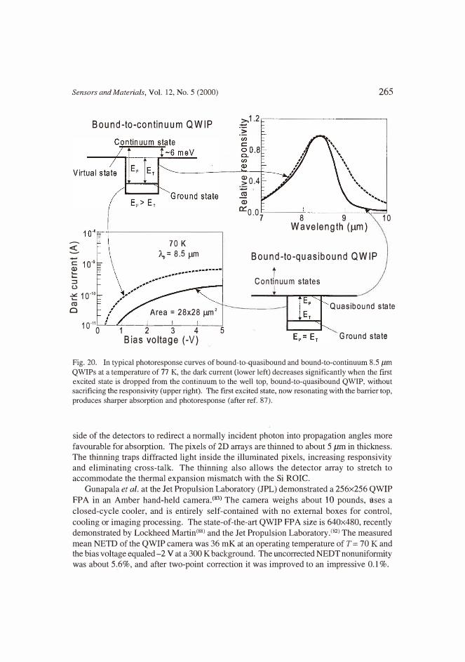
Sensors and Materials, Vol. 12, No. 5 (2000)
Bound-to-continuum QW IP
-
::5,
C 10·9 (l) ,._
,._
::::,
(.)
� 10·10
ctl Cl
70 K \= 8.5 µm
Area = 28x28 µm 2
1 o-11=------�--�-�,---�-� 0 1 2 3 4 5Bias voltage (-V)
�1.2
-�
�0.4
� (l)
c:: 0.07
265
8 9 10 Wavelength (µm)
Bound-to-quasibound QWIP
i Continuum states
Quasibound state
Ground state
Fig. 20. In typical photoresponse curves of bound-to-quasibound and bound-to-continuum 8.5 µrn
QWIPs at a temperature of 77 K, the dark current (lower left) decreases significantly when the first
excited state is dropped from the continuum to the well top, bound-to-quasibound QWIP, without sacrificing the responsivity (upper right). The first excited state, now resonating with the barrier top,
produces sharper absorption and photoresponse (after ref. 87).
side of the detectors to redirect a normally incident photon into propagation angles more favourable for absorption. The pixels of 2D arrays are thinned to about 5 µm in thickness. The thinning traps diffracted light inside the illuminated pixels, increasing responsivity and eliminating cross-talk. The thinning also allows the detector array to stretch to accommodate the thermal expansion mismatch with the Si ROIC.
Gunapala et al. at the Jet Propulsion Laboratory (JPL) demonstrated a 256x256 QWIP FPA in an Amber hand-held camera.(83l The camera weighs about 10 pounds, ases a closed-cycle cooler, and is entirely self-contained with no external boxes for control, cooling or imaging processing. The state-of-the-art QWIP FPA size is 640x480, recently demonstrated by Lockheed Martin(88l and the Jet Propulsion Laboratory.C82l The measured mean NETD of the QWIP camera was 36 mK at an operating temperature of T = 70 K and the bias voltage equaled-2 Vat a 300 K background. The uncorrected NEDT nonuniforrnity was about 5.6%, and after two-point correction it was improved to an impressive 0.1 %.
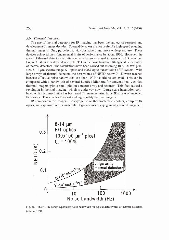
266 Sensors and Materials, Vol. 12, No. 5 (2000)
5.6. Thermal detectors
The use of thermal detectors for IR imaging has been the subject of research and
development for many decades. Thermal detectors are not useful for high-speed scanning
thermal imagers. Only pyroelectric vidicons have found more widespread use. These
devices achieved their fundamental limits of performance by about 1970. However, the
speed of thermal detectors is quite adequate for non-scanned imagers with 2D detectors.
Figure 21 shows the dependence of NETD on the noise bandwith for typical detectivities of thermal detectors. The calculations have been carried out assuming 1OOx100 µm2 pixel
size, 8-14 µm spectral range, f/1 optics and 100% optic transmission ofIR system. With
large arrays of thermal detectors the best values of NETD below 0.1 K were reached
because effective noise bandwidths less than 100 Hz could be achieved. This can be
compared with a bandwidth of several hundred kilohertz for conventionally cooled
thermal imagers with a small photon detector array and scanner. This fact caused a
revolution in thermal imaging, which is underway now. Large-scale integration combined with micromachining has been used for manufacturing large 2D arrays of uncooled
IR sensors. This enables low-cost and high-quality thermal imagers.
IR semiconductor imagers use cryogenic or thermoelectric coolers, complex IR
optics, and expensive sensor materials. Typical costs of cryogenically cooled imagers of
0.3
--.
::::s:::::
�0.2 1-
w z
0.1
8-14 µmF/1 optics
100x100 µm2
pixeltop
= 100%
0 '----------'-------------'----'------'-----------
10 100 Noise bandwidth (Hz)
1000
Fig. 21. The NETD versus equivalent noise bandwidth for typical detectivities of thermal detectors
(after ref. 89).
Sensors and Materials, Vol. 12, No. 5 (2000) 267
around $50,000 restrict their installation to critical military applications allowing operations to be conducted in complete darkness. Very encouraging results have been obtained with micromachined silicon bolometer arrays and pyroelectric detector arrays. Several countries have demonstrated imagers with NETO of 100 mK or better, and the cost of simple systems is sometimes below $10,000. It is expected that costs of high-performance imager systems will be reduced to less than $1,000 and IR cameras will become widely available in the near future. Although developed for military applications, lowcost IR imagers are likely to be used in nonmilitary applications such as drivers aid, aircraft aid, industrial process monitoring, community services, firefighting, portable mine detection, night vision, border surveillance, law enforcement, search and rescue, and others.
5.6.1 Micromachined silicon bolometers
Honeywell Sensor and System Development ·center in Minneapolis began developing silicon micromachined IR sensors in the early 1980s. The goal of the work, sponsored by DARPA and the US Army Night Vision and Electronic Sensors Directorate, was to produce low-cost night-vision systems amenable to wide use throughout the military with NETD of 0.1 °C using f/1 optics. Both Si bolometer arrays and pyroelectric a1nys from Texas Instruments (TI) have exceeded that goal. c9oJ The micro bolometer will have the lowest unit cost, as it uses a monolithic fabrication process that is compatible with the standard silicon process on 8" or greater wafers. Chopperless operation can be obtained using the microbolometer, thereby eliminating all mechanical parts from the sensor. This not only decreases the ultimate unit cost, but improves both the reliability and operating range. The greater dynamic range and more linear response make the microbolometer technology more highly suited for applications like mine detection, target signature, radiometric measurement, process control and facilities/equipment maintenance.
In practice, two options for the detector structure are used: microbridge (see Fig. 22) and pellicle-supported designs. The former comprises detector elements which are supported on legs above the plane of the microcircuit. The legs are designed to have a high thermal resistance and to carry electrical conductors from the detector to the microcircuit. This approach is applied in the Honeywell microbolometer design. The second concept consists of detector elements deposited onto a thin dielectric pellicle coplanar with the surface of the wafer.
Probably the most popular thermistor material used in the fabrication of micromachined silicon bolometers is vanadium dioxide, V02. Vanadium is a metal with a variable valence that forms a large number of oxides. The preparation of these materials in both bulk and thin film forms is very difficult, given the narrowness of the stability range of any oxide. Vanadium dioxide undergoes its transition in the temperature range from about 50 to 70°C. The resistivity change and optical properties of V02 films strongly depend on the fabrication conditions and the resulting crystallographic structure and stoichiometry. From the point of view of IR imaging applications, probably the most important property of V02 is its high negative temperature coefficient of resistance (TCR) at ambient temperature, which exceeds 4% per degree for a single element bolometer and about 2% for FPA.
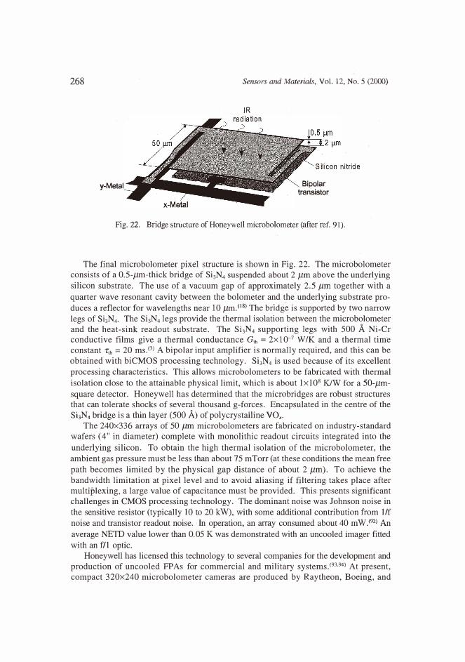
268
y-Metal
Sensors and Materials, Vol. 12, No. 5 (2000)
JR
Bipolar transistor
Fig. 22. Bridge structure of Honeywell microbolometer (after ref. 91).
The final microbolometer pixel structure is shown in Fig. 2 2 . The microbolometer consists of a 0.5-µm-thick bridge of Si3N4 suspended about 2 µm above the underlying silicon substrate. The use of a vacuum gap of approximately 2 .5 µm together with a quarter wave resonant cavity between the bolometer and the underlying substrate produces a reflector for wavelengths near 10 µm.08) The bridge is supported by two narrowlegs of Si3N4. The Si3N4 legs provide the thermal isolation between the microbolometer and the heat-sink readout substrate. The Si3N4 supporting legs with 500 A Ni-Cr conductive films give a thermal conductance G,h = 2x10- 7 WIK and a thermal time constant r1h = 20 ms. c3> A bipolar input amplifier is normally required, and this can be obtained with biCMOS processing technology. Si3N4 is used because of its excellent processing characteristics. This allows microbolometers to be fabricated with thermal isolation close to the attainable physical limit, which is about lxl0 8 KJW for a 50-µm
square detector. Honeywell has determined that the microbridges are robust structures that can tolerate shocks of several thousand g-forces. Encapsulated in the centre of the Si3N4 bridge is a thin layer (500 A) of polycrystalline VO •.
The 240x336 arrays of 50 µm microbolometers are fabricated on industry-standard wafers (4" in diameter) complete with monolithic readout circuits integrated into the underlying silicon. To obtain the high thermal isolation of the microbolometer, the ambient gas pressure must be less than about 75 mTorr (at these conditions the mean free path becomes limited by the physical gap distance of about 2 µm). To achieve the bandwidth limitation at pixel level and to avoid aliasing if filtering takes place after multiplexing, a large value of capacitance must be provided. This presents significant challenges in CMOS processing technology. The dominant noise was Johnson noise in the sensitive resistor (typically 10 to 20 kW), with some additional contribution from 1/f noise and transistor readout noise. In operation, an atrny consumed about 40 mW.192) An average NETD value lower than 0.05 K was demonstrated with an uncooled imager fitted with an f/1 optic.
Honeywell has licensed this technology to several companies for the development and production of uncooled FPAs for commercial and military systems.<93•94) At present, compact 320x240 microbolometer cameras are produced by Raytheon, Boeing, and
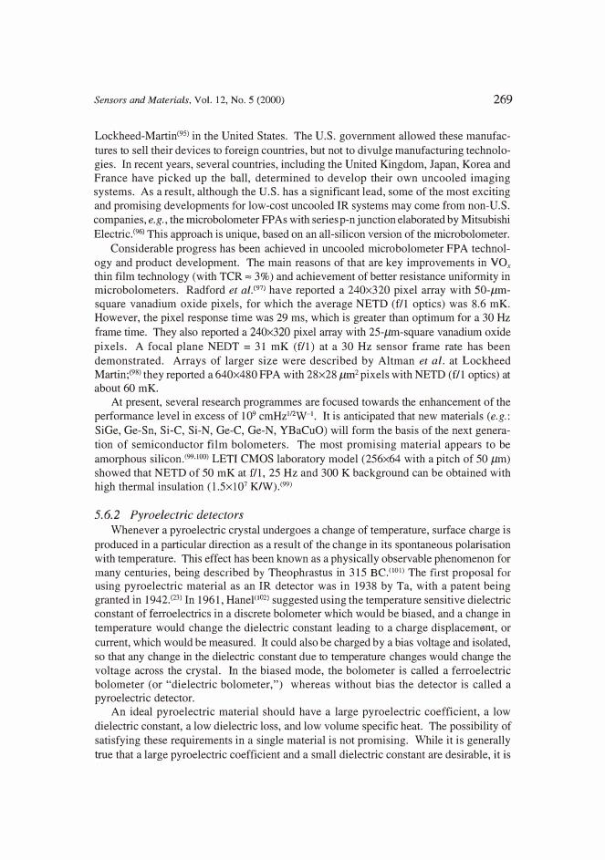
Sensors and Materials, Vol. 12, No. 5 (2000) 269
Lockheed-MartinC95l in the United States. The U.S. government allowed these manufactures to sell their devices to foreign countries, but not to divulge manufacturing technologies. In recent years, several countries, including the United Kingdom, Japan, Korea and France have picked up the ball, determined to develop their own uncooled imaging systems. As a result, although the U.S. has a significant lead, some of the most exciting and promising developments for low-cost uncooled IR systems may come from non-U.S. companies, e.g., the rnicrobolometer FPAs with series p-njunction elaborated by Mitsubishi Electric.C96l This approach is unique, based on an all-silicon version of the rnicrobolometer.
Considerable progress has been achieved in uncooled micro bolometer FP A technology and product development. The main reasons of that are key improvements in VOx
thin film technology (with TCR"" 3%) and achievement of better resistance uniformity in microbolometers. Radford et az.c97l have reported a 240x320 pixel array with 50-µm
square vanadium oxide pixels, for which the average NETD (f/1 optics) was 8.6 mK. However, the pixel response time was 29 ms, which is greater than optimum for a 30 Hz frame time. They also reported a 240x320 pixel array with 25-µm-square vanadium oxide pixels. A focal plane NEDT = 31 mK (f/1) at a 30 Hz sensor frame rate has been demonstrated. Arrays of larger size were described by Altman et al. at Lockheed Martin;C98l they reported a 640x480 FPA with 28x28 µm2 pixels with NETD (f/1 optics) at about 60 mK.
At present, several research programmes are focused towards the enhancement of the performance level in excess of 109 cmHz112w -1• It is anticipated that new materials (e.g.: SiGe, Ge-Sn, Si-C, Si-N, Ge-C, Ge-N, YBaCuO) will form the basis of the next generation of semiconductor film bolometers. The most promising material appears to be amorphous silicon_c99
,1oo) LETI CMOS laboratory model (256x64 with a pitch of 50 µm)
showed that NETD of 50 mK at f/1, 25 Hz and 300 K background can be obtained with high thermal insulation ( l .5x107 K/W).<99)
5.6.2 Pyroelectric detectors
Whenever a pyroelectric crystal undergoes a change of temperature, surface charge is produced in a particular direction as a result of the change in its spontaneous polarisation with temperature. This effect has been known as a physically observable phenomenon for many centuries, being described by Theophrastus in 315 BC.< 1011 The first proposal for using pyroelectric material as an IR detector was in 1938 by Ta, with a patent being granted in 1942.<231 In 1961, Hanei<1021 suggested using the temperature sensitive dielectric constant of ferroelectrics in a discrete bolometer which would be biased, and a change in temperature would change the dielectric constant leading to a charge displacem@t, or current, which would be measured. It could also be charged by a bias voltage and isolated, so that any change in the dielectric constant due to temperature changes would change the voltage across the crystal. In the biased mode, the bolometer is called a ferroelectric bolometer (or "dielectric bolometer,") whereas without bias the detector is called a pyroelectric detector.
An ideal pyroelectric material should have a large pyroelectric coefficient, a low dielectric constant, a low dielectric loss, and low volume specific heat. The possibility of satisfying these requirements in a single material is not promising. While it is generally true that a large pyroelectric coefficient and a small dielectric constant are desirable, it is
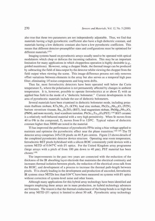
270 Se_nsors and Materials, Vol. 12, No. 5 (2000)
also true that these two parameters are not independently adjustable. Thus, we find that materials having a high pyroelectric coefficient also have a high dielectric coristant, and materials having a low dielectric constant also have a low pyroelectric coefficient. This means that different detector-preamplifier sizes and configurations must be optimised for different materials. oo3)
Imaging systems based on pyroelectric arrays usually need to be operated with optical modulators which chop or defocus the incoming radiation. This may be an important limitation for many applications in which chopperless operation is highly desirable (e.g.,
guided munitions). However, using a chopper blade, the thermal image can be produced by subtracting the field of data output by the detector whilst viewing the chopper from the field output when viewing the scene. This image-difference process not only removes offset variations between elements in the array but also serves as a temporal high pass filter, eliminating 1/f noise components and long term drifts.
Thus far, most ferroelectric detectors have been operated well below the Curie temperature Tc, where the polarisation is not permanently affected by changes in ambient temperature. It is, however, possible to operate ferroelectrics at or above Tc with an applied bias field in the mode of a "dielectric bolometer." Current developments in the area of pyroelectric materials include the use of dielectric bolometers.
Several materials have been examined in dielectric bolometer mode, including potassium thallium niobate, KTaxNb 1_xO3 (KTN), lead zinc niobate, Pb(Zn113Nb213)O3 (PZN), barium strontium titanate, Ba1_xSrxTiO3 (BST), lead magnesium niobate, Pb(Mg113Nb213)O3,
(PMN), and more recently, lead scandium tantalate, Pb(Sc112Ta 112)OJ(PST).0°4l BST ceramic is a relatively well-behaved material with a very high permittivity. When Sr moves from 40 to 0% in the compound, Tc moves from Oto 120°C. Typical values of dielectric constant higher than 30000 are noted in the material.
TI has improved the performance of pyroelectric FP As using a bias voltage applied to maintain and optimise the pyroelectric effect near the phase transition. oo5-107) The TI detector array comprises 245x328 pixels on 48.5 µm centres. Figure 23 shows details of the completed pyroelectric detector device structure. Operating near room temperature, ferroelectric BST pixels hybridised with a silicon ROIC consistently yield devices with a system NETD of 0.047°C with f/1 optics. For the United Kingdom array programme
(large arrays with a pitch of from 100 µm down to 40 µm), PST material has been chosen.<108l
The improvements in the past two years are connected with the reduction of the thickness of the IR absorbing layer electrode that maintains the electrical continuity and increases thermal isolation between pixels, the reduction of the electrical cross-talk from the ROIC, and development of a process to increase the thermal path-length between pixels. TI is clearly leading in the development and production of uncooled, ferroelectric IR systems since NETDs less than 0.04°C have been measured on systems with f/1 optics
without correction of system-level noise and other losses. Although many applications for this hybrid array technology have been identified and
imagers employing these arrays are in mass production, no hybrid technology advances are foreseen. The reason is that the thermal conductance of the bump bonds is so high that the array NETD (f/1 optics) is limited to about 50 mK. Pyroelectric array technology
Sensors and Materials, Vol. 12, No. 5 (2000)
Semi-transparent metal
Organic
Reflecting metal
Fig. 23. BST dielectric bolometer pixel (after ref. 105).
271
therefore is moving toward a monolithic silicon microstructure technology.< 107•108) Themicrobridge structures are preferable to pellicles on wells etched into the silicon, since the
competition in area for readout circuitry forces a poor pixel FF. The monolithic process should have fewer steps and a shorter cycle time. The detector cost in high volume will be limited primarily by detector packaging costs, which are not significantly different for hybrid and monolithic arrays. Most ferroelectrics tend to lose their interesting properties as the thickness is reduced. However, some ferroelectric materials seem to maintain their properties better than others. This seems particularly true for lead titanate (PbTiO3) and related materials, whereas BST, the material used in hybrid detectors, does not hold its
properties well in thin-film form. Various techniques for the deposition of thin ferroelectric films have been investigated, including radio-frequency magnetron sputtering, dual ion beam sputtering, sol-gel processing and laser ablation.
Recently, initial imaging monolithic 240x320 arrays have been produced by Raytheon. <109i The fe1rnelectric material, modified lead titanate, was applied by a spin-onmetal-organic decomposition method. In this process an aqueous solution is spun onto the wafer using a modified photoresist track. The film is subjected to a pyrolysis process,
which removes the organic materials. The arrays produced to date have demonstrated an NEDT of about 400 mK with operability in excess of 95%. The sensitivity is poor for several reasons: thermal isolation has not received its potential value, IR absorption is only 20%, and the pyrolysis process is not optimal.
5.6.3 Novel sensors
Datskos et az.<110> have proposed a new method for photon detection using electronic(photo-induced) stress in microstructures. Photo-induced stress in semiconductor micro-
272 Sensors and Materials, Vol. 12, No. 5 (2000)
structures is caused by changes in the charge carrier density in the conduction band, and photon detection results from the measurement of the photo-induced bending of semiconductor microstructures. The microstructures can be fabricated using standard semiconductor methods and materials and as a consequence could be mass produced at very low cost.
Another example of a recent technological thrust which has generated IR detector concepts is micro-electromechanical structures (MEMSs). This technology is a marriage of photolithography and mechanics. Micro-bimaterial structures have been built with MEMSs for evaluation as IR sensors.<111J FPAs based on MEMS technology and a visible optical readout system may offer lower cost L WIR imaging systems.
5.7 Mainstream FPA technologies Recent efforts in the technology of infrared detectors have mostly been focused on
large electronically scanned FPAs. The increased sensitivity and resolution in the system complexity of FP As offer significant advantages in military as well as civilian applications in thermal imaging, guidance, reconnaissance, surveillance, ranging and communication systems. For IR imaging systems, the relevant figure of merit for determining the ultimate performance is not the detectivity O* but the NETO.
Figure 24 shows a plot of the thermal detectivity (300 K, 0° FOV) versus operating temperature for the most pruminent detector technologies. The thermal detectivity is used here to compare the various technologies with equivalent NETO irrespective of wavelength. The thermal D* figure of merit for photon detectors was obtained by equating theNETD of an ideal them1al detector for a given D* to the NETD of an ideal photon detectot with the given O\
p- The various regions show the appropriate applications including
"low-cost" uncooled thermal detectors, "high-performance uncooled" (SWIR InGaAs and HgCdTe photodiodes) for night vision enhancement and ,earth reconnaissance, "tactical" for most imaging uses, and "strategic" for various military instruments. For "lowcost" applications, the imagery is limited by thermal conduction to the pixels. Photocurrent shot noise should limit the detectivity for other thermal imagers. Strategic sensors generally detect point targets, so the D* must be as high as possible within the constraint that the cooler must not pose overriding issues of size, weight, reliability or cost. High performance near IR has similar performance requirements, but can only provide a minimum of cooling because cost and weight minimisation is critical. The extrinsic silicon detectors offer very high sensitivity but at a very low operating temperature which is prohibitive in most applications. The cryogenically cooled InSb and HgCdTe arrays have comparable array size and pixel yield in the MWIR spectral band. However, wavelength tunability and high quantum efficiency have made HgCdTe the preferred material. This material assures the highest possible operating temperature for a given set of operating conditions. Thus, the associated cooling and system power requirements can be optimally distributed. The monolithic PtSi Schottky barrier FPAs lead all other technologies with respect to array size(> 106 pixels); however, the thermal mismatch barrier in hybrid FP As has been recently overcome by developers (lnSb and HgCdTe arrays).
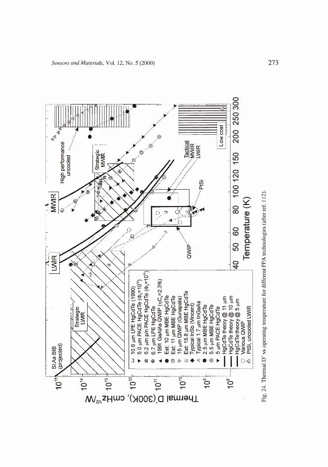
� �N
I
E
0
- � 0
0
C")
1014
1013
- ·o
1011
co E Q)10
10
.c
1-
109 ,_
108
10.6
µm
LP
E H
gC
dTe
(19
90)
.,,
5.0
µm
PA
CE
Hg
Cd
Te (<I>
b=10
12
)
Ill
5.2
µm p
/n P
AC
E H
gC
dTe
(<I>
b=10
12
)
+6.
7 µ
m L
PE
Hg
Cd
Te.._
19
91 G
aA
IAs
QW
IP (T]
Cp=
2.3
%)
e
Est
: 10
µm
MBE
Hg
Cd
Te®
E
st 1
1 µm
MBE
Hg
Cd
Tev
15
µm
QW
IP (G
una
pala
)II]
Est
15.
8 µ
m M
BE H
gC
dTe
+Ty
pica
l lnS
b (
Vin
cent
)Ty
pica
l 1.7
µm
lnG
aA
se
2.
5 µ
m M
BE
Hg
Cd
Te
5.5
µm M
BE H
gC
dTe
.,,
5
µm P
AC
E H
gC
dTe
-
Hg
Cd
Te th
eor
y @
11
µm-
Hg
Cd
Te th
eor
y @
1 0
µm
-H
gC
dTe
the
ory
@ 5
µm
0
Var
iou
s Q
WIP
b.P
tSi,
unc
oole
d L
WIR
40 Q
WIP
Hig
h pe
rfor
ma
nce
u
ncoo
led
PtS
i
Tact
ica
l M
WIR
L
WIR
Low
co
st
50
60
80
10
0 12
0
150
2
00
2
50 3
00
Te
mp
era
ture
(K
)
Fig
. 24.
The
rmal
D*
vs
ope
rati
ng t
empe
ratu
re f
or d
iffe
rent
FP
A tec
hno
logi
es (
afte
r re
f. 1
12
).
� � � �- _1;;" � � z
!:l
u,
,;::::, 8 8 N
-..J
<.,.)
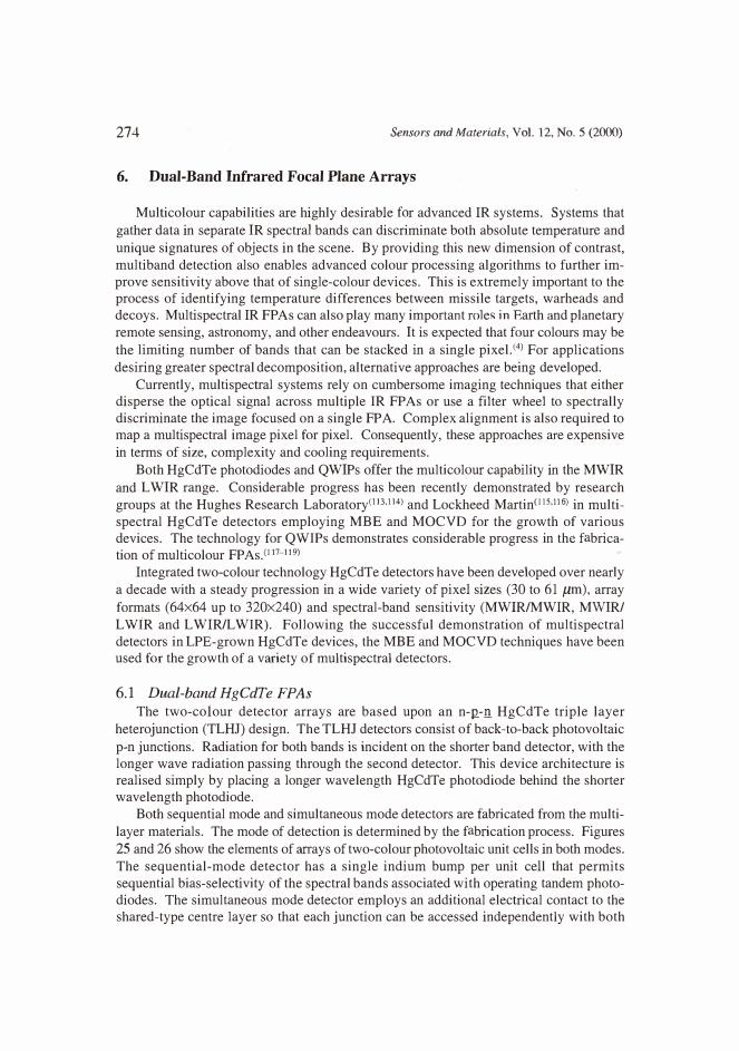
274 Sensors and Materials, Vol. 12, No. 5 (2000)
6. Dual-Band Infrared Focal Plane Arrays
Multicolour capabilities are highly desirable for advanced IR systems. Systems that gather data in separate IR spectral bands can discriminate both absolute temperatur� and unique signatures of objects in the scene. By providing this new dimension of contrast, multiband detection also enables advanced colour processing algorithms to further improve sensitivity above that of single-colour devices. This is extremely important to the process of identifying temperature differences between missile targets, warheads and decoys. Multispectral IR FP As can also play many important roles in Earth and planetary remote sensing, astronomy, and other endeavours. It is expected that four colours may be the limiting number of bands that can be stacked in a single pixel. C4) For applicationsdesiring greater spectral decomposition, alternative approaches are being developed.
Currently, multispectral systems rely on cumbersome imaging techniques that either disperse the optical signal across multiple IR FPAs or use a filter wheel to spectrally discriminate the image focused on a single FP A. Complex alignment is also required to map a multispectral image pixel for pixel. Consequently, these approaches are expensive in terms of size, complexity and cooling requirements.
Both HgCdTe photodiodes and QWIPs offer the multicolour capability in the MWIR and L WIR range. Considerable progress has been recently demonstrated by research groups at the Hughes Research LaboratoryC113•114) and Lockheed Martincu5 ,116l in multispectral HgCdTe detectors employing MBE and MOCVD for the growth of various devices. The technology for QWIPs demonstrates considerable progress in the fabrication of multicolour FPAs.<117-119)
Integrated two-colour technology HgCdTe detectors have been developed over nearly a decade with a steady progression in a wide variety of pixel sizes (30 to 61 µm), array formats (64x64 up to 320x240) and spectral-band sensitivity (MWIR/MWIR, MWIR/ LWiR and LWIR/LWIR). Following the successful demonstration of multispectral detectors in LPE-grown HgCdTe devices, the MBE and MOCVD techniques have been used for the growth of a variety of multispectral detectors.
6.l Dual-band HgCdTe FPAs
The two-coiour detector arrays are based upon an n-Il.-.!1 HgCdTe triple layerheterojunction (TLHJ) design. The TLHJ detectors consist of back-to-back photovoltaic p-n junctions. Radiation for both bands is incident on the shorter band detector, with thelonger wave radiation passing through the second detector. This device architecture isrealised simply by placing a longer wavelength HgCdTe photodiode behind the shorterwavelength photodiode.
Both sequential mode and simultaneous mode detectors are fabricated from the multilayer materials. The mode of detection is determined by the fabrication process. Figures 25 and 26 show the elements of arrays of two-colour photovoltaic unit cells in both modes. The sequential-mode detector has a single indium bump per unit cell that permits sequential bias-selectivity of the spectral bands associated with operating tandem photodiodes. The simultaneous mode detector employs an additional electrical contact to the shared-type centre layer so that each junction can be accessed independently with both
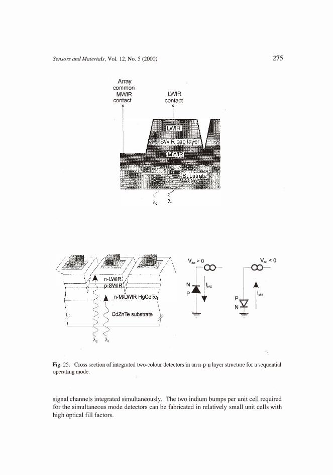
Sensors and Materials, Vol. 12, No. 5 (2000) 275
Array common
MWIR LWIR contact contact
'-_, 1 \
'.'.'/ \ \ ) ( CdZnTe substrate . l<)' ,)
-;;( < I
?
vdet > 0 Vd., < O
1· ···� "i i '� r� p t p
N ---
Fig. 25. Cross section of integrated two-colour detectors in an n-12-n layer structure for a sequential operating mode.
signal channels integrated simultaneously. The two indium bumps per unit cell required for the simultaneous mode detectors can be fabricated in relatively small unit cells with high optical fill factors.
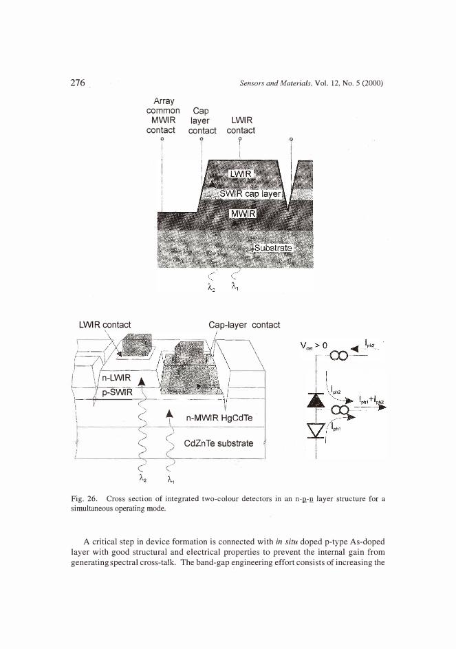
276
LWI R contact \
\ }__//
Array common
MWIR contact
f-7\ \I "-----�f-f I ; \ If-------<
I \/ n-LWIR 1------'1--�;-:---;:=--+'---\ } p-SWIR1-7
• "--.,
< �
( ,->
< A-;
t
< ()
A.1
Sensors and Materials, Vol. 12, No. 5 (2000)
Cap layer
contact LWIR
contact
! i
Cap-layer contact I 1,�--�
/ '\
n-MWIR HgCdTe
CdZnTe substrate 'f
Fig. 26. Cross section of integrated two-colour detectors in an n-n-n layer structure for a
simultaneous operating mode.
A critical step in device formation is connected with in situ doped p-type As-doped layer with good structural and electrical properties to prevent the internal gain from generating spectral cross-talk. The band-gap engineering effort consists of increasing the
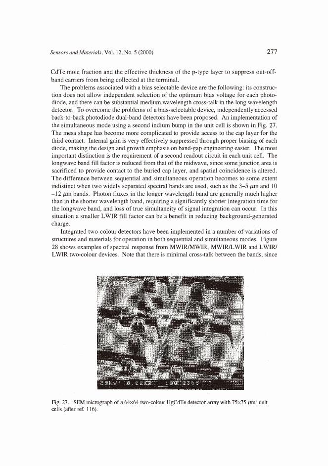
Sensors and Materials, Vol. 12, No. 5 (2000) 277
CdTe mole fraction and the effective thickness of the p-type layer to suppress out-off
hand carriers from being collected at the terminal.
The problems associated with a bias selectable device are the following: its construction does not allow independent selection of the optimum bias voltage for each photodiode, and there can be substantial medium wavelength cross-talk in the long wavelength detector. To overcome the problems of a bias-selectable device, independently accessed back-to-back photodiode dual-band detectors have been proposed. An implementation of the simultaneous mode using a second indium bump in the unit cell is shown in Fig. 27. The mesa shape has become more complicated to provide access to the cap layer for the
third contact. Internal gain is very effectively suppressed through proper biasing of each diode, making the design and growth emphasis on band-gap engineering easier. The most important distinction is the requirement of a second readout circuit in each unit cell. The longwave band fill factor is reduced from that of the mid wave, since some junction area is sacrificed to provide contact to the buried cap layer, and spatial coincidence is altered.
The difference between sequential and simultaneous operation becomes to some extent
indistinct when two widely separated spectral bands are used, such as the 3-5 µm and 10
-12 µm bands. Photon fluxes in the longer wavelength band are generally much higherthan in the shorter wavelength band, requiring a significantly shorter integration time forthe longwave band, and loss of true simultaneity of signal integration can occur. In thissituation a smaller L WIR fill factor can be a benefit in reducing background-generatedcharge.
Integrated two-colour detectors have been implemented in a number of variations of
structures and materials for operation in both sequential and simultaneous modes. Figure
28 shows examples of spectral response from MWIR/MWIR, MWIR/L WIR and L WIR/ LWIR two-colour devices. Note that there is minimal cross-talk between the bands, since
Fig. 27. SEM micrograph of a 64x64 two-colour HgCdTe detector array with 75x75 µm2 unit cells (after ref. 116).
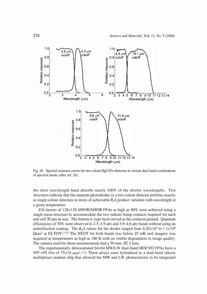
278
1.0
Q) 0.8(/)
0
fil- 0.6 � Q)
,$ 0.4 (I!
Q)
o: 0.2
3 4 5
Wavelength (µm)
1.0
Q) 0.8(/)
0
fil- 0.6 � ,$ 0.4 (I!
Q) 0:
0.2
8.6 µm cutoff
Sensors and Materials, Vol. 12, No. 5 (2000)
1.0
4.9µm Q) 0.8 cutoff (/)
fil- 0.6�
,E 0.4(I!
Q)
o: 0.2
6 O.O 2 3 4 5 6 7 8 9 10 11 12 13 14 Wavelength (µm)
0·02 3 4 5 6 7 8 910 11 121314
Wavelength (µm)
Fig. 28. Spectral response curves for two-colour HgCdTe detectors in various dual-band combinations of spectral bands (after ref. 29).
the short wavelength band absorbs nearly 1 00% of the shorter wavelengths. Test structures indicate that the separate photodiodes in a two-colour detector perform exactly as single-colour detectors in terms of achievable RoA product variation with wavelength at a given temperature.
Fill factors of 128x128 MWIR/MWIR FPAs as high as 80% were achieved using a single mesa structure to accommodate the two indium bump contacts required for each unit cell 50 µm in size. The bottom n -type layer served as the common ground. Quantum efficiencies of70% were observed in 2.5-3.9 µm and 3.9-4.6 µm bands without using an antireflection coating. The RoA values for the diodes ranged from 8.25x10⁵ to l.l x106
Qcm2 at f/2 FOV.<114l The NEDT for both bands was below 25 mK and imagery was acquired at temperatures as high as 180 K with no visible degradation in image quality . The camera used for these measurements had a 50 mm, f/2.3 lens.
The experimentally demonstrated 64x64 MW/LW dual-band MOCVD FPAs have a unit cell size of 75x75 mm2 .c116l These arrays were hybridised to a dual-band siliconmultiplexer readout chip that allowed the MW and L W photocurrents to be integrated
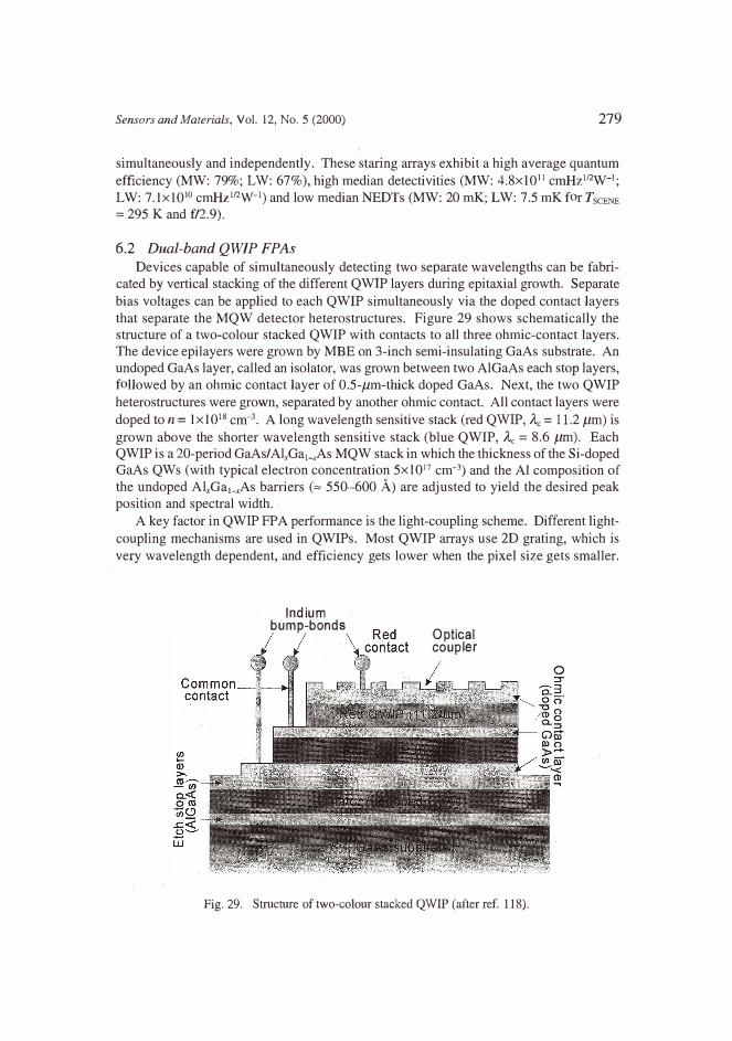
Sensors and Materials, Vol. 12, No. 5 (2000) 279
simultaneously and independently. These staring arrays exhibit a high average quantum efficiency (MW: 79%; LW: 67%), high median detectivities (MW: 4.8x10 11 cmHz112W -1 ;
LW: 7.lxl0 10 cmHz 112w-1) and low median NEDTs (MW: 20 mK; LW: 7.5 mK for TscENE
= 295 Kand f/2 .9).
6.2 Dual-band QWIP FPAs
Devices capable of simultaneously detecting two separate wavelengths can be fabricated by vertical stacking of the different QWIP layers during epitaxial growth. Separate bias voltages can be applied to each QWIP simultaneously via the doped contact layers that separate the MQW detector heterostructures. Figure 29 shows schematically the structure of a two-colour stacked QWIP with contacts to all three ohmic-contact layers. The device epilayers were grown by MBE on 3-inch semi-insulating GaAs substrate. An undoped GaAs layer, called an isolator, was grown between two AlGaAs each stop layers, followed by an ohmic contact layer of 0 .5 -µm-thick doped GaAs. Next, the two QWIP heterostructures were grown, separated by another ohmic contact. All contact layers were doped ton= lxl0 18 cm- 3
• A long wavelength sensitive stack (red QWIP, Ac
= 11.2 µm) is grown above the shorter wavelength sensitive stack (blue QWIP, Ac
= 8.6 µm). Each QWIP is a 20-period GaAs/AlxGa1_xAs MQW stack in which the thickness of the Si-doped GaAs QWs (with typical electron concentration 5xl0 17 cm-3) and the Al composition of the undoped AlxGa 1_xAs barriers ("' 550:-600 A) are adjusted to yield the desired peak position and spectral width.
A key factor in QWIP FPA performance is the light-coupling scheme. Different lightcoupling mechanisms are used in QWIPs. Most QWIP arrays use 2D grating, which is very wavelength dependent, and efficiency gets lower when the pixel size gets smaller.
Indium bump-bonds
Optical coupler
Fig. 29. Structure of two-colour stacked QWIP (after ref. 118).
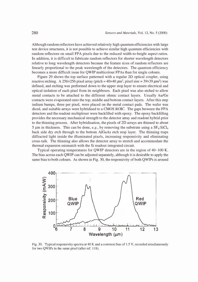
280 Sensors and Materials, Vol. 12, No. 5 (2000)
Although random reflectors have achieved relatively high quantum efficiencies with large test device structures, it is not possible to achieve similar high quantum efficiencies with random reflectors on small FP A pixels due to the reduced width-to-height aspect ratios.
In addition, it is difficult to fabricate random reflectors for shorter wavelength detectors
relative to long wavelength detectors because the feature sizes of random reflectors are linearly proportional to the peak wavelength of the detectors. The quantum efficiency becomes a more difficult issue for QWIP multicolour FPAs than for single colours.
Figure 29 shows the top surface patterned with a regular 2D optical coupler, using reactive etching. A 256x256 pixel array (pitch= 40x40 µm2
, pixel size= 39x39 µm2) was defined, and etching was performed down to the upper stop layer to ensure electrical and optical isolation of each pixel from its neighbours. Each pixel was also etched to allow
metal contacts to be attached to the different ohmic contact layers. Usually Au/Ge contacts were evaporated onto the top, middle and bottom contact layers. After this step indium bumps, three per pixel, were placed on the metal contact pads. The wafer was diced, and suitable arrays were hybridised to a CMOS ROIC. The gaps between the FPA detectors and the readout multiplexer were backfilled with epoxy. The epoxy backfilling provides the necessary mechanical strength to the detector array and readout hybrid prior to the thinning process. After hybridisation, the pixels of 2D arrays are thinned to about
5 µm in thickness. This can be done, e.g., by removing the substrate using a SF6:SiC14
back side dry etch through to the bottom AlGaAs etch stop layer. The thinning traps diffracted light inside the illuminated pixels, increasing responsivity and eliminating cross-talk. The thinning also allows the detector array to stretch and accommodate the thermal expansion mismatch with the Si readout integrated circuit.
Typical operating temperatures for QWIP detectors are in the region of 40-100 K. The bias across each QWIP can be adjusted separately, although it is desirable to apply the
same bias to both colours. As shown in Fig. 30, the responsivity of both QWIPs is around
-
<C 300E -
:� 200 Cl) C:
0 c..
� 100 c::::
7 8 9 10 11 Wavelength (µm)
12 13
Fig. 30. Typical responsivity spectra at 40 Kand a common bias of 1.5 V, recorded simultaneously
for two QWIPs in the same pixel (after ref. 118).
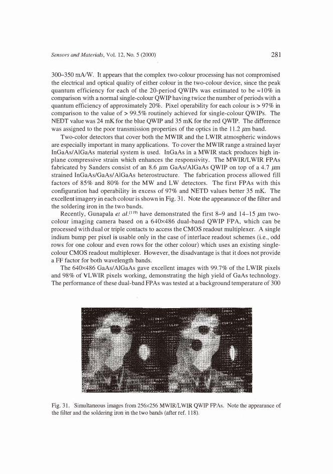
Sensors and Materials, Vol. 12, No. 5 (2000) 281
300-350 rnA/W. It appears that the complex two-colour processing has not compromised
the electrical and optical quality of either colour in the two-colour device, since the peak
quantum efficiency for each of the 20-period QWIPs was estimated to be ael0% incomparison with a normal single-colour QWIP having twice the number of periods with aquantum efficiency of approximately 20%. Pixel operability for each colour is > 97% in comparison to the value of> 99.5% routinely achieved for single-colour QWIPs. The
NEDT value was 24 mK for the blue QWIP and 35 mK for the red QWIP. The difference
was assigned to the poor transmission properties of the optics in the 11.2 µm band.
Two-color detectors that cover both the MWIR and the L WIR atmospheric windows
are especially important in many applications. To cover the MWIR range a strained layer InGaAs/AlGaAs material system is used. InGaAs in a MWIR stack produces high inplane compressive strain which enhances the responsivity. The MWIR/LWIR FPAs fabricated by Sanders consist of an 8.6 µm GaAs/AlGaAs QWIP on top of a 4.7 µm strained InGaAs/GaAs/ AlGaAs heterostructure. The fabrication process allowed fill
factors of 85% and 80% for the MW and LW detectors. The first FPAs with this
configuration had operability in excess of 97% and NETD values better 35 mK. The
excellent imagery in each colour is shown in Fig. 31. Note the appearance of the filter and the soldering iron in the two bands.
Recently, Gunapala et az.c119> have demonstrated the first 8-9 and 14-15 µm twocolour imaging camera based on a 640x486 dual-band QWIP FPA, which can be
processed with dual or triple contacts to access the CMOS readout multiplexer. A single
indium bump per pixel is usable only in the case of interlace readout schemes (i.e., odd
rows for one colour and even rows for the other colour) which uses an existing single
colour CMOS readout multiplexer. However, the disadvantage is that it does not provide a FF factor for both wavelength bands.
The 640x486 GaAs/AlGaAs gave excellent images with 99.7% of the LWIR pixels and 98% of VLWIR pixels working, demonstrating the high yield of GaAs technology. The performance of these dual-band FP As was tested at a background temperature of 300
Fig. 31. Simultaneous images from 256x256 MWIR/LWlR QWIP FPAs. Note the appearance of the filter and the soldering iron in the two bands (after ref. 118).
282 Sensors and Materials, Vol. 12, No. 5 (2000)
K with an f/2 cold stop and at a frame rate of 30 Hz. The mean value of the L WIR FP A quantum efficiency is 12.9% at an operating temperature of T = 40 K, and a bias V8 = -2
V. This integrated quantum efficiency includes 30% substrate reflection and 85% FPA
fill factor. The uncorrected nonuniformity of the quantum efficiency histogram is 2%.
The mean quantum efficiency of 14-15 µm detector pixels in the FPA is 8.9%, and the
uncorrected quantum efficiency nonuniformity is about 1 %. The estimated NEDT ofLWIR and VLWIR detectors at 40 K are 36 and 44 mK, respectively.
7. Anticipated Evolution oflnfrared Technology in the Near Future
The future applications of IR detector systems require: • higher pixel sensitivity,• further increases in pixel density to above 106 pixels,• cost reduction in IR imaging array systems through the use of less cooling sensortechnology combined with the integration of detectors and signal processing functions(with much more on-chip signal processing),• improvements in the functionality of IR imaging arrays through development of
multispectral sensors.
To reduce the real cost of the IR images systems, one must consider all the elements
which make up the cost to the user. The cost can be broken down into four parts: the chip (detector+ ROIC), the dewar, integration and tests. The user must add the cryogenic machine cost that is not negligible compared to the components. This explains why the cost of PtSi or QWIPs is not markedly less than that of photon detectors of the same
complexity, even though the raw materials (silicon and GaAs) are much less than for
HgCdTe. In addition, since PtSi requires a very wide optical aperture to obtain acceptable
performance, and since QWIP requires a lower operating temperature than the other
photon detectors, a possible reduction in the purchase price is counterbalanced by a significant increase in operating costs.020l
Detector maturity is a function of the accumulated experience and development effort, the complexity of the device required, and the inherent difficulty presented by the material technology. At present, HgCdTe photodiodes and BIB extrinsic silicon detectors are not
fully mature. PtSi technology is mature and has achieved a plateau. Other two detector
technologies such as InSb and silicon bolometers are still evolving significantly as
applications for larger array configurations and smaller pixel sizes continue to push the technology. Other mature technologies such as PbS, PbSe and HgCdTe photoconductors have been significantly enhanced in their performance in the last 30 years in response to demands for higher responsivity, lower 1/f noise, better uniformity, and greater
produci bility.
Thermal detector arrays will increase in size and improve in thermal sensitivity to a
level satisfying high performance applications at ambient temperature. It is assumed that
the silicon rnicrobolometers arrays and the monolithic pyroelectric arrays will capture the low-cost markets. Current uncooled bolometer FP As have achieved NETDs less than 10 mK with f/1 optics, which opens the door to the use of less expensive, slower optical systems. Generally, in comparison with photon detectors, the performance of thermal
Sensors and Materials, Vol. 12, No. 5 (2000) 283
detector is modest, they suffer from slow response, and they are not very useful in applications requiring multispectral detection.
At present, the Cadillac 2000 car offers an IR imaging system based on TI pyroelectric 240x320 hybrid FPAs.<121) Within a decade such systems will be standard equipment in luxury cars and optional equipment in almost all models. IR imagery gives the driver the ability to see several times further ahead than with headlights, and the relative distance advantage will probably be even greater under weather conditions such as fog. It is supposed that sales of IR imaging equipment to the automobile market will begin to rapidly change the relative ratio between military/government and commercial IR markets_C4l Today only about 10% of the market is commercial. After a decade the commercial market can grow to over 70% in volume and 40% in value, largely connected with volume production of uncooled imagers for automobiles. With large volume production for automobiles, the cost of uncooled imaging systems will decrease to below $1,000. Of course, these systems will cover other segments of the transportation industry: trucks, trains, ships, barges, buses, and airplanes. The cheapest uncooled IR imagers will be deployed for everyday tasks, including amusement. Perhaps MEMS technology will allow direct-view sensors to be built which can be used like optical binoculars.<4l
The main drawback of uncooled thermal detectors is their slow response speed. For same applications requiring uncooled detectors, the slow response speed is unacceptable. Recently, a number of concepts (e.g., non-equilibrium devices,<47) multi-junction HgCdTephotodiodes,(122) optical immersion) and new materials (InAsSb, InAs/GaSb-based type IIsuperlattices023l) have been proposed to improve the performance of photon detectorsoperating at near room temperature. The measurements show the possibility to achieve detectivity of"" lx109 cmHzll2fW at the 8-9 µm range, and potentially the devices can be assembled in large FPAs.< 123l These new possibilities will outperform the present day performance of uncooled thermal detectors.
Despite serious competition from alternative technologies and slower progress than expected, HgCdTe is unlikely to be seriously challenged for high-performance applications, applications requiring multispectral capability and fast response. The recent successes of competing cryogenically cooled detectors are due to technological, not fundamental, issues. There are good reasons to think that the steady progress in epitaxial technology will make HgCdTe devices much more affordable in the near future. The much higher operation temperature of HgCdTe compared to Schottky barrier devices and low-dimensional solid devices may become a decisive argument in this case.
The fundamental performance limits of HgCdTe photodiodes have not yet been reached. Further progress will be in the direct proportional to the amount of effort directed toward basic materials science and processing technology. Continued development of in situ vapour phase epitaxy (MBE and MOCVD) will allow bandgap engineering of heterojunction devices of increasing quality and complexity. Continued development of epitaxial growth on alternative substrates such as silicon will also reduce the cost of 2D arrays. SWIR arrays will be developed for starlight imaging applications in the 1-2.5 µm region. Efforts to extend the useful cutoff wavelength to beyond the present 17 µm will continue. Higher operating temperatures will continue to receive attention, through the reduction of Shockley-Read defects as well as unique device heterostructures. Develop-
284 Sensors and Materials, Vol. 12, No. 5 (2000)
ment of dual-band arrays will continue, and three-band detectors will soon be demonstrated. To provide high-resolution spectroscopic imaging, larger HgCdTe FP As will be
used in Fourier-transform (FT) interferometers. Photodiodes will replace photoresistors
for detection out to 15 µm, since they are characterized by a more linear response.
The situation concerning quantum well structures and superlattices is not clear;
however, unique detection capabilities may arise from low-dimensional solids. The situation for LWIR QWIPs is clear. The initial results show promise for the growth of QWIPs on silicon wafers and applications for integration with silicon-based electronics.c124l It is expected that a QWIP hand-held, cost-effective camera will find imaging and
spectroscopy applications in the L WIR spectral band. The powerful possibilities of
QWIP technology are connected with VL WIR FPA applications and with multicolour
detection. Three-band and four-band FPAs will soon be demonstrated in the near future.
Finally, considerable development of signal processing functions into FPAs can be anticipated. Many devices today have digital programming interfaces to control readout operation (integration, scan direction, gain adjustment, and others). The next few years
will see on-chip analogue-to-digital conversion become commonplace, followed by
nonuniformity correction.
Acknowledgement
This work was partially supported by the Polish State Committee for Scientific Research (Poland) under grant number PBZ 28. l l/P6.
References
W. Herschel: Phil. Trans. Roy. Soc. London 90 (1800) 255.
2 R. A. Smith, F. E. Jones and R. P. Chasmar: The Detection and Measurement of Infrared Radiation (Clarendon, Oxford, 1958).
3 P. W. Kruse, L. D. McGlauchlin and R. B. McQuistan: Elements of Infrared Technology (Wiley, New York, 1962).
4 P.R. Norton: Proc. SPIE 3698 (1999) 652-665.
5 E. S. Barr: Amer. J. Phys. 28 (1960) 42-54.
6 E. S. Barr: Infrared Phys. 2 (1962) 67-73.
7 E. S. Barr: Infrared Phys. 3 (1963) 195-206.
8 T. W. Case: Phys. Rev. 9 (1917) 305-310. 9 R. J. Cushman: Proc. IRE 47 (1959) 1471-1475.
10 W. S. Boyle and G. E. Smith: Bell Syst. Tech. J. 49 (1970) 587-593. 11 F. Shepherd and A. Yang: IEDM Tech. Dig. (1973) 310-313.
12 W. D. Lawson, S. Nielson, E. H. Putley and A. S. Young: J. Phys. Chem. Solids 9 (1959) 325-329.
13 M. J.E. Golay: Rev. Sci. Instr. 18 (1947) 357-362.
14 E. M. Wormser: J. Opt. Soc. Amer. 43 (1953) 15-21.
15 G. W. McDaniel and D. Z. Robinson: Appl. Opt. 1 (1962) 311-324. 16 C. Hilsum and W.R. Harding: Infrared Phys. 1 (1961) 67-93. 17 A. J. Goss: Proc. SPIE 807 (1987) 25-32. 18 R. A. Wood: Monolithic silicon microbolometer arrays in Semiconductors and Semimetals,
Sensors and Materials, Vol. 12, No. 5 (2000) 285
Vol. 47 eds. P. W. Kruse and D. D. Skatrud (Academic Press, San Diego, 1997) 45-121.
19 C. M. Hanson: Hybrid pyroelectric-ferroelectric bolometer arrays in Semiconductors and Semimetals Vol. 47 eds. P. W. Kruse and D. D. Skatrud (Academic Press, San Diego, 1997) 123-174.
20 P. W. Kruse: Opto-Electr. Rev. 7 (1999) 253-258. 21 R. A. Wood and N. A. Foss: Laser Focus World (June, 1993) 101-106.
22 A. Rogalski: Infrared Detectors (Gordon and Breach Science Publishers, Amsterdam, 2000).
23 M. Razeghi: Opto-Electr. Rev. 6 (1998) 155-194.
24 D. A. Scribner, M. R. Kruer and J.M. Killiany: Proc. IEEE 79 (1991) 66-85.
25 L. J. Kozlowski, J.M. Arias, G. M. Williams, K. Vural, D. E. Cooper, S. A. Cabelli and C.
Bruce: Proc. SPIE 2274 (1994) 93-116.
26 I. M. Baker and R. A. Ballinga: Proc. SPIE 510 (1984) 121-129. 27 B. Ewing: Photonics Spectra (July 1990) 85-92. 28 N. Yutani, H. Yagi, M. Kimata, J. Nakanishi, S. Nagayoshi and N. Tsubouchi: IEDM Tech.
Digest (1991) 175-178.
29 P.R. Norton: Proc. SPIE 3379 (1998) 102-114.
30 K. Vural, L. J. Kozlowski, D. E. Cooper, C. A. Chen, G. Bostrup, C. Cabelli, J. M. Arias, J.
Bajaj, K. W. Hodapp, D. N. B. Hall, W. E. Kleinhans, G. G. Price and J. A. Pinter: Proc. SPIE 3698 (1999) 24-35.
31 J. L. Miller: Principles oflnfrared Technology (Van Nostrand Reinhold, New York, 1994). 32 L. J. Kozlowski, J. Montroy, K. Vural and W. E. Kleinhans: Proc. SPIE 3436 (1998) 162-171. 33 L. J. Kozlowski, K. Vural, J. Luo, A. Tomasini, T. Liu and W. E. Kleinhans: Opto-Electr. Rev.
7 (1999) 259-269.
34 E. R. Fossum: Proc. SPIE 1900 (1993) 2-14.
35 E. R. Fossum and B. Pain: Proc. SPIE 2020 (1993) 262-285 .
36 M. J. Hewitt, J. L. Vampola, S. H. Black and C. J. Nielsen: Proc. SPIE 2226 (1994) 108-119.
37 L. J. Kozlowski, S. A. Cabelli, D. E. Cooper and K. Vural: Proc. SPIE 1946 (1993) 199-213. 38 J. L. Vampola: Readout electronics for infrared sensors in The Infrared and Electro-Optical
Systems Handbook, Vol. 3 eds. J. S. Accetta and D. L. Shumaker (Infrared Information
Analysis Center, Ann Arbor, and SPIE Optical Engineering Press, Bellingham, 1993) 285-342. 39 L. J. Kozlowski and W. F. Kosonocky: Infrared detector arrays in Handbook of Optics, eds. M.
Bass, E.W. Van Stryland, D.R. Williams and W. L. Wolfe (McGraw-Hill, New York, 1995)
Chap. 23.
40 M. Kimata and N. Tubouchi: Charge transfer devices in Infrared Photon Detectors, ed. A.
Rogalski (SPIE Optical Engineering Press, Bellingham, 1995) 99-144. 41 J. Bajaj: State-of-the-art HgCdTe materials and devices for infrared imaging in Physics of
Semiconductor Devices, eds. Vikram Kumar and S. K. Agarwal (Narosa Publishing House, New Delhi, 1998) 1297-1309.
42 F. D. Shepherd and A. C. Yang: Tech. Digest ofIEDM (1973) 310-313. 43 A. Rogalski: New Ternary Alloy Systems for Infrared Detectors (SPIE Optical Engineering
Press, Bellingham, 1994).
44 A. Rogalski: Hg-based alternatives to HgCdTe in Infrared Detectors and Emitters: Materials and Devices, eds. P. Capper and C. T. Elliott (Kluwer Academic Publishers, Boston, 2000).
45 J. L. Lee, J. D. Kim and M. Razeghi: Opto-Electr. Rev. 7 (1999) 19-28.
46 J. Piotrowski and W. Gawron: Infrared Phys. Technol. 38 (1997) 63-68. 47 T. C. Elliott: Proc. SPIE 3436 (1998) 763-775. 48 A. Rogalski: Infrared Phys. Technol. 38 (1997) 295-310.
49 W. E. Tennant, C. A. Cockrum, J.B. Gilpin, M.A. Kinch, M. B. Reine and R. P. Ruth: J. Vac.
Sci. Technol. BlO (1992) 1359-1369.
286 Sensors and Materials, Vol. 12, No. 5 (2000)
50 A. Rogalski and R. Ciupa: J. Appl. Phys. 77 (1995) 3505-3512. 51 A. Rogalski: Infared Phys. Technol. 41 (2000) 213-238.
52 K. Vural: Opt. Eng. 26 (1987) 201-208.
53 L. J. Kozlowski, R. B. Bailey, S. A. Cabelli, D. E. Cooper, I. S. Gergis, A. C. Chen, W. V.
McLevige, G. L. Bostrup, K. Vural, W. E. Tennant and P.H. Howard: Opt. Eng. 33 (1994) 54-
63. 54 T. Tung, L. V. DeArmond, R. F. Herald, P. E. Heming, M. H. Kalisher, D. A. Olson, R. F.
Risser, A. P. Stevens and S. J. Tighe: Proc. SPIE 1735 (1992) 109-134. 55 T. J. de Lyon, R. D. Rajavel, J. A. Vigil, J.E. Jensen, 0. K. Wu, C. A. Cockrum, S. M. Johnson,
G. M. Venzor, S. L. Bailey, I. Kasai, W. L. Ahlgren and M. S. Smith: J. Electron. Mater. 27
(1998) 550-555 .
56 L. J. Kozlowski, K. Vural, D. Q. Bui, R. B. Bailey, D. E. Cooper and D. M. Stephenson: Proc.
SPIE 1946 (1993) 148-160.
57 L. J. Kozlowski, K. Vural, S. C. Cabelli, C. Y. Chen, D. E. Cooper, G. L. Bostrup, D. M. Stephenson, W. L. McLevige, R. B. Bailey, K. Hodapp, D. Hall and W. E. Kleinhans: Proc. SPIE 2268 (1994) 353-364 .
58 L. 0. Bubulac, W. E. Tennant, J. G. Pasko, L. J. Kozlowski, M. Zandian, M. E. Motamedi, R. E. De Warnes, J. Bajaj, N. Nayar, W. V. McLevige, N. S. Gluck, R. Melendes, D. E. Cooper, D. D. Edwall, J.M. Arias and R. Hall: J. Electron. Mater. 26 (1997) 649-655 .
59 A. Rogalski and R. Ciupa: J. Electron. Mater. 28 (1999) 630--636.
60 W. F. Kosonocky: Optoelectronics-Devices and Technologies 6 (1991) 173-203 .
61 M. Denda, M. Kimata, S. I wade, N. Yutani, T. Kondo and N. Tsubouchi: IEEE Trans. Electron Devices 38 (1991) 1145-1151.
62 M. T. Daigle, D. Colvin, E.T. Nelson, S. Brickman, K. Wong, S. Yoshizumi, M. Elzinga, P. Sorlie, D. Rockafellow, T. Travers andR. Avel: Proc. SPIE 1308 (1990) 88-98.
63 M. Kimata and N. Tsubouchi: Schottky barrier photoemissive detectors in Infrared Photon Detectors, ed A. Rogalski (SPIE Optical Engineering Press, Bellingham, 1995) pp. 299-349.
64 M. Kimata, M. Ueno, H. Yagi, T. Shiraishi, M. Kawai, K. Endo, Y. Kosasayama, T. Sone, T.
Ozeki and N. Tsubouchi: Opto-Electr. Rev. 6 (1998) 1-10 .
65 M. Inoue, T. Seto, S. Takahashi, S. Itoh, H. Yagi, T. Siraishi, K. Endo and M. Kimata: Proc. SPIE 3061 (1997) 150--158 .
66 H. Wada, M. Nagashima, K. Hayashi, J. Nakanishi, M. Kimata, N. Kumada and S. Ito: OptoElectr. Rev. 7 (1999) 305�311.
67 A. G. U. Perera: Physics and novel device applications of semiconductor homojunctions in
Thin Solid Films, Vol. 21, eds. M. H. Francombe andJ. L. Vossen (Academic Press, New York
1995) 1-75.
68 A.G. H. Perera and W. Z. Shen: Opto-Electr. Rev. 7 (1999) 153-180.
69 M. D. Petroff and M. G. Stapelbroeck: Blocked impurity band detectors U.S. Patent No. 4 568 960, filed 23 October 1980, granted 4 February 1986.
70 S. B. Stetson, D. B. Reynolds, M. G. Stapelbroeck and R. L. Stermer: Proc. SPIE 686 (1986) 48-65.
71 D. B. Reynolds, D. H. Seib, S. B. Stetson, T. L. Herter, N. Rowlands and J. Schoenwald: IEEE Trans. Nucl. Sci. 36 (1989) 857-862.
72 J.E. Huffman, A.G. Crouse, B. L. Halleck, T. V. Downes and T. L. Herter: J. Appl. Phys. 72
(1992) 273-275.
73 D. M. Watson and J.E. Huffman: Appl. Phys. Lett. 52 (1988) 1602-1604. 74 D. M. Watson, M. T. Guptill, J.E. Huffman, T. N. Krabach, S. N. Raines and S. Satyapal: J.
Appl. Phys. 74 (1993) 4199-4206.
Sensors and Materials, Vol. 12, No. 5 (2000) 287
75 I. C. Wu, J. W. Beeman, P. N. Luke, W. L. Hansen and E. E. Haller: Appl. Phys. Lett. 58 (1991)
1431-1433.
76 F. Szmulowicz and F. L. Madarsz: J. Appl. Phys. 62 (1987) 2533-2540.
77 J. Venzon, N. Lum, S. Freeman and G. Domingo: Proc. SPIE 2475 (1995) 34-40.
78 S. Solomon, A. Tribble, N. Lum, J. Venzon, G. Domingo, A. Hofman and M. Smith: Proc. SPIE
2816 (1996) 161-168.
79 M. G. Stapelbroeck, D. H. Seib, J.E. Huffman and R. A. Florence: Proc. SPIE 2476 (1995) 41-
48.
80 M. Davis, M. Greiner, J. Sanders and J. Wimmers: Proc. SPIE 3379 (1998) 288-299.
81 A. M. Fowler, I. Gatley, P. McIntyre, F. J. Vrba and A. Hoffman: Proc. SPIE 2816 (1996) 150-
160 . 82 S. D. Gunapala, S. V. Bandara, J. K. Liu, W. Hong, E. M. Luong, J.M. Mumolo, M. J.
McKelvey, D. K. Sengupta, A. Singh, C. A. Shott, R. Carralejo, P. D. Maker, J. J. Bock, M. E.
Ressler, M. W. Werner and T. N. Krabach: Proc. SPIE 3379 (1998) 382-395 .
83 S. Gunapala, S. Bandara, J. Liu and M. Sundaram: Opto-Electr. Rev. 7 (1999) 271-282.
84 S. D. Gunapala, S. V. Bandara, A. Sigh, J. K. Liu, S. B. Rafol, E. M. Luong, J.M. Mumolo, N.
Q. Tran, J. D. Vincent, C. A. Shott, J. Long and P. D. Le Van: Proc. SPIE 3698 (1999) 687-697.
85 M. Z. Tidrow, W. A. Beck, W.W. Clark, H. K. Pollehn, J. W. Little, N. K. Dhar, P. R. Leavitt,
S. W. Kennerly, D. W. Beekman, A. C. Goldberg and W.R. Dyer: Opto-Electr. Rev. 7 (1999) 283-296.
86 A. Rogalski: Infrared Phys. Technol. 40 (1999) 279-294. 87 S. Gunapala, M. Sundaram and S. Bandara: Laser Focus World (June 1996) 233-240.
88 W. A. Beck and T. S. Faska: Proc. SPIE 2744 (1996) 193-206.
89 R. Watton and M. V. Mansi: Proc. SPIE 865 (1987) 78-85.
90 R. E. Flannery and J.E. Miller: Proc. SPIE 1689 (1992) 379-395.
91 R. A. Wood, C. J. Han and P. W. Kruse: Proc. IEEE Solid State Sensor and Actuator Workshop,
Hilton Head Island, S. C. (June, 1992) 132-135.
92 R. A. Wood: Proc. SPIE 2020 (1993) 322-329. 93 W. Radford, D. Murphy, A. Finch, A. Kennedy, J. Kojiro, M. Ray, R. Wyles, R. Coda, E.
Moody and S. Baur: Proc. SPIE 3379 (1998) 22-35.
94 P. E. Howard, C. J. Han, J. E. Clarke, J. C. Stevens, P. Ely and E. T. Fitzgibbons: Proc. SPIE
3379 (1998) 47-57.
95 P. W. Kruse: Opto-Electr. Rev. 7 (1999) 253-258.
96 T. Ishikawa, M. Ueno, K. Endo, Y. Nakaki, H. Hata, T. Sane and M. Kimata: Opto-Electron.
Rev. 7 (1999) 297-303.
97 W. Radford, D. Murphy, A. Finch, K. Hay, A. Kennedy, M. Ray, A. Sayed, J. Wyles, R. Wyles, J. Varesi, E. Moody and F. Cheung: Proc. SPIE 3698 (1999) 119-130.
98 M. Altman, B. Backer, M. Kohin, R. Blackwell, N. Butler and J. Cullen: Proc. SPIE 3698
(1999) 137-143.
99 C. Vedel, J. L. Martin, J. L. Ouvrier Buffet, J. L. Tissot, M. Vilan and J. J. Yon: Proc. SPIE 3698
(1999) 276-283.
100 J. Brady, T. Schimert, D. Ratcliff, R. Gooch, B. Ritchey, P. McCardel, K. Rachels, S. Rapson,
M. Wand, M. Weinstein and J. Wynn: Proc. SPIE 3698 (1999) 161-167.
101 S. B. Lang: Ferroelectrics 7 (1974) 231-234.
102 R. A. Hanel: J. Opt. Soc. Amer. 51 (1961) 220-225 . 103 R. W. Whatmore: Rep. Prog. Phys. 49 (1986) 1335-1386.
104 R. W. Whatmore: Ferroelectrics 118 (1991) 241-259.
105 C. M. Hanson: Proc. SPIE 2020 (1993) 330-339.
106 H. Betatan, C. Hanson and E.G. Meissner: Proc. SPIE 2274 (1994) 147-156.
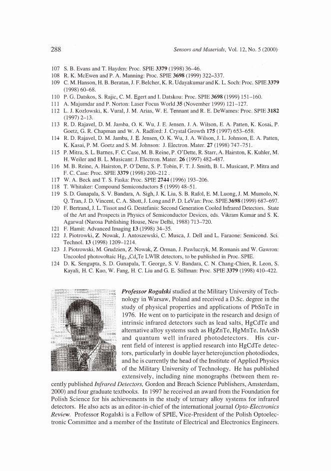
288 Sensors and Materials, Vol. 12, No. 5 (2000)
107 S. B. Evans and T. Hayden: Proc. SPIE 3379 (1998) 36-46.
108 R. K. McEwen and P.A. Manning: Proc. SPIE 3698 (1999) 322-337.
109 C. M. Hanson, H.B. Beratan, J. F. Belcher, K. R. Udayakumar and K. L. Soch: Proc. SPIE 3379
(1998) 60--68.
110 P. G. Datskos, S. Rajic, C. M. Egert and I. Datskou: Proc. SPIE 3698 (1999) 151-160.
111 A. Majumdar and P. Norton: Laser Focus World 35 (November 1999) 121-127.
112 L. J. Kozlowski, K. Vural, J.M. Arias, W. E. Tennant and R. E. DeWames: Proc. SPIE 3182
(1997) 2-13. 113 R. D. Rajavel, D. M. Jarnba, 0. K. Wu, J.E. Jensen, J. A. Wilson, E. A. Patten, K. Kosai, P.
Goetz, G. R. Chapman and W. A. Radford: J. Crystal Growth 175 (1997) 653-658.
114 R. D. Rajavel, D. M. Jamba, J.E. Jensen, 0. K. Wu, J. A. Wilson,.J. L. Johnson, E. A. Patten,
K. Kasai, P. M. Goetz and S. M. Johnson: J. Electron. Mater. 27 (1998) 747-751.
115 P. Mitra, S. L. Barnes, F. C. Case, M. B. Reine, P. O'Dette, R. Starr, A. Hairston, K. Kuhler, M.
H. Weiler and B. L. Musicant: J. Electron. Mater. 26 (1997) 482-487.
116 M. B. Reine, A. Hairston, P. O'Dette, S. P. Tobin, F. T. J. Smith, B. L. Musicant, P. Mitra and F. C. Case: Proc. SPIE 3379 (1998) 200--212 .
117 W. A. Beck and T. S. Faska: Proc. SPIE 2744 (1996) 193-206. 118 T. Whitaker: Compound Semiconductors 5 (1999) 48-51.
119 S. D. Gunapala, S. V. Bandara, A. Sigh, J. K. Liu, S. B. Rafol, E. M. Luong, J.M. Mumolo, N.
Q. Tran, J. D. Vincent, C. A. Shott, I.Long and P. D. Le Van: Proc. SPIE 3698 (1999) 687-697.
120 F. Bertrand, J. L. Tissot and G. Destefanis: Second Generation Cooled Infrared Detectors. State of the Art and Prospects in Physics of Semiconductor Devices, eds. Vikram Kumar and S. K.
Agarwal (Narosa Publishing House, New Delhi, 1988) 713-720. 121 F. Hamit: Advanced Imaging 13 (1998) 34-35. 122 J. Piotrowki, Z. Nowak, J. Antoszewski, C. Musca, J. Dell and L. Faraone: Semicond. Sci.
Technol. 13 (1998) 1209-1214.
123 J. Piotrowski, M. Gmdzien, Z. Nowak, Z. Orman, J. Pawluczyk, M. Romanis and W. Gawron:
Uncooled photovoltaic Hg1_,Cd,Te LWIR detectors, to be published in Proc. SPIE.
124 D. K. Sengupta, S. D. Gunapala, T. George, S. V. Bandara, C. N. Chang-Chien, R. Leon, S.
Kayali, H. C. Kuo, W. Fang, H. C. Liu and G. E. Stillman: Proc. SPIE 3379 (1998) 410-422.
Professor Roga/,ski studied at the Military University of Technology in Warsaw, Poland and received a D.Sc. degree in the
study of physical properties and applications of PbSnTe in
1976. He went on to participate in the research and design of
intrinsic infrared detectors such as lead salts, HgCdTe and alternative alloy systems such as HgZnTe, HgMnTe, InAsSb and quantum well infrared photodetectors. His current field of interest is applied research into HgCdTe detectors, particularly in double layer heterojunction photodiodes,
and he is currently the head of the Institute of Applied Physics
of the Military University of Technology. He has published extensively, including nine monographs (between them re,.
cently published Infrared Detectors, Gordon and Breach Science Publishers, Amsterdam, 2000) and four graduate textbooks. In 1997 he received an award from the Foundation for Polish Science for his achievements in the study of ternary alloy systems for infrared detectors. He also acts as an editor-in-chief of the international journal Opto-Electronics
Review. Professor Rogalski is a Fellow of SPIE, Vice-President of the Polish Optoelectronic Committee and a member of the Institute of Electrical and Electronics Engineers.
Related Documents