Industrial Affiliates Workshop, March 2004 Planar Ion-Exchanged Glass Waveguide Devices Seppo Honkanen, Brian West and Sanna Yliniemi Optical Sciences Center University of Arizona Collaborators: Nasser Peyghambarian, Ray Kostuk, David Geraghty, Axel Schulzgen, Mike Morrell (University of Arizona)

Industrial Affiliates Workshop, March 2004 Planar Ion-Exchanged Glass Waveguide Devices Seppo Honkanen, Brian West and Sanna Yliniemi Optical Sciences.
Dec 18, 2015
Welcome message from author
This document is posted to help you gain knowledge. Please leave a comment to let me know what you think about it! Share it to your friends and learn new things together.
Transcript

Industrial Affiliates Workshop, March
2004
Planar Ion-Exchanged Glass Waveguide Devices
Seppo Honkanen, Brian West and Sanna Yliniemi
Optical Sciences Center
University of Arizona
Collaborators:
Nasser Peyghambarian, Ray Kostuk, David Geraghty,
Axel Schulzgen, Mike Morrell (University of Arizona)

Industrial Affiliates Workshop, March
2004
Outline
• Introduction• Ion Exchange Glass Waveguide
Technology– Molten Salt Process
– Extensive Process -and Device Modeling– Study on Waveguide Birefringence
– Dry Ag-Film Process– MM-diode pumped Er-doped Waveguide Lasers
• Outlook and Conclusion
2

Industrial Affiliates Workshop, March
2004
Ti MaskDeposition
Na+
Ag+
MaskPatterning
IonExchange
MaskRemoval
Field-Assisted
Burial
• Waveguides Defined by Standard Photolithography
• Simple Processing
• Potential for Adjustment Through Annealing
Molten Salt Ion Exchange
3

Industrial Affiliates Workshop, March
2004
Binary Ion Exchange
Diffusion Equation
kT
CEq
C
CC
C
D
t
C Aext
A
AA
A
AA .
1
)(
1
22
• CA = normalized concentration of in-diffusing ions
• DA = self-diffusion coefficient of in-diffusing ions
• DB = self-diffusion coefficient of out-diffusing ions
• α = 1 - DA/DB
• q = electron charge
• k = Boltzmann’s constant
• T = absolute temperature
• Eext = externally applied electric field
4
Industrial Affiliates Workshop, March
2004
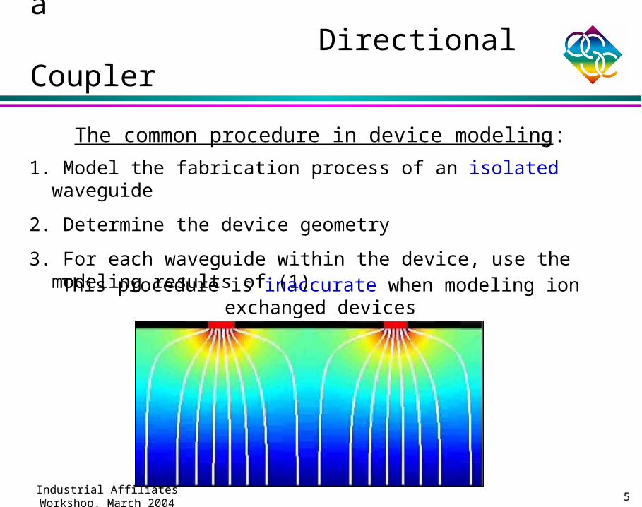
Example: Process Modeling for a Directional Coupler
The common procedure in device modeling: 1. Model the fabrication process of an isolated waveguide
2. Determine the device geometry
3. For each waveguide within the device, use the modeling results of (1)
This procedure is inaccurate when modeling ion exchanged devices
5

Industrial Affiliates Workshop, March
2004
Concentration and Mode Profiles
3 μm mask opening 9 μm mask opening
6
Industrial Affiliates Workshop, March
2004
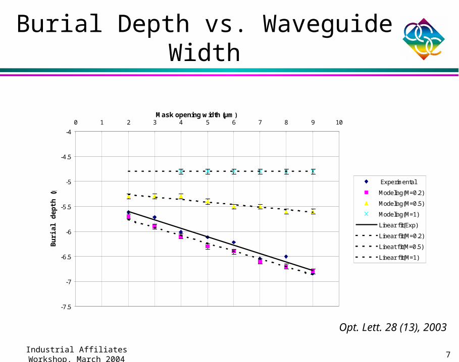
Burial Depth vs. Waveguide Width
-7.5
-7
-6.5
-6
-5.5
-5
-4.5
-4
0 1 2 3 4 5 6 7 8 9 10Mask opening width (µm)
Bu
ria
l de
pth
(µ
m)
Experimental
Modeling(M=0.2)
Modeling(M=0.5)
Modeling(M=1)
Linear f it(Exp)
Linear f it(M=0.2)
Lineat f it(M=0.5)
Linear f it(M=1)
Opt. Lett. 28 (13), 2003
7

Industrial Affiliates Workshop, March
2004
Waveguide Birefringence
8

Industrial Affiliates Workshop, March
2004
Selectively Buried Waveguides
Glass
Polymer
Polymer-Glass Modulator
Masking During Burial:
9

Industrial Affiliates Workshop, March
2004
Adiabatic VerticalWaveguide Transition
10
Industrial Affiliates Workshop, March
2004
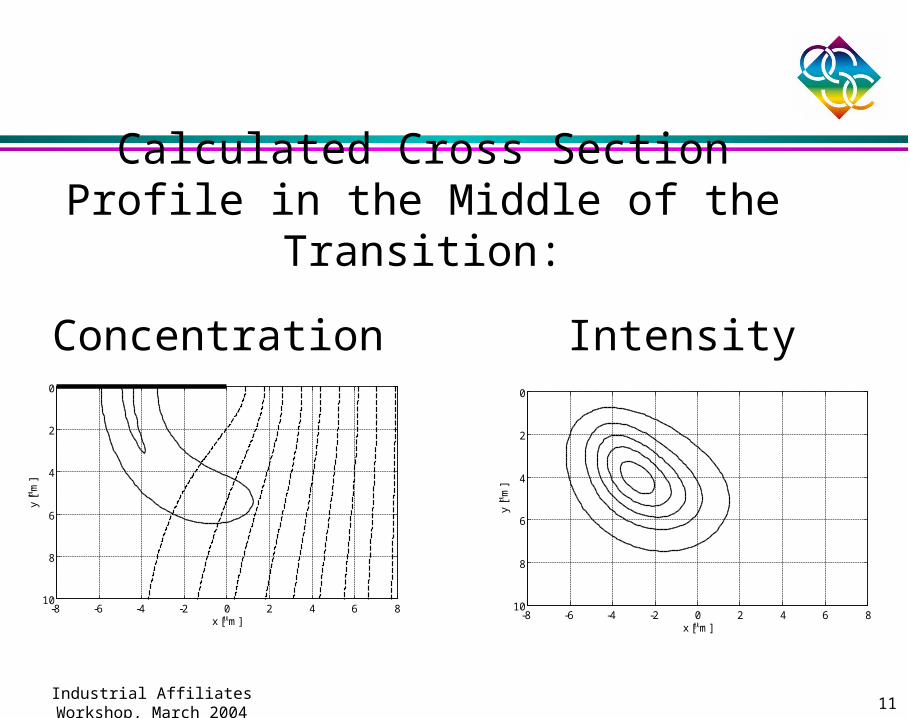
Calculated Cross Section Profile in the Middle of the Transition:
-8 -6 -4 -2 0 2 4 6 8
0
2
4
6
8
10
x [m]
y [
m]
-8 -6 -4 -2 0 2 4 6 8
0
2
4
6
8
10
x [m]
y [
m]
Concentration Intensity
11
Industrial Affiliates Workshop, March
2004
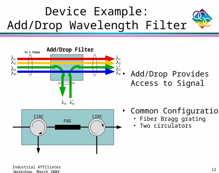
Device Example:Add/Drop Wavelength Filter
12
34
12
4
3 3'
3'
Add/Drop FilterIn 1 Fiber
• Add/Drop Provides Access to Signal
• Common Configuration• Fiber Bragg grating• Two circulators
FBGCIRC CIRC
12

Industrial Affiliates Workshop, March
2004
Asymmetric Y-BranchAdd/Drop Filter
Output
AddDrop
Input
OutputInput
On Resonance
Off Resonance
• Asymmetric Y branches• Wide guide excites even mode• Narrow guide excites odd mode• Bi-directional
• Tilted Grating• Breaks orthogonality of 2 modes
• Benefits• Ion-Exchanged Waveguides• Single component• Structures defined photolithographically• Possible mass integration
13
Industrial Affiliates Workshop, March
2004
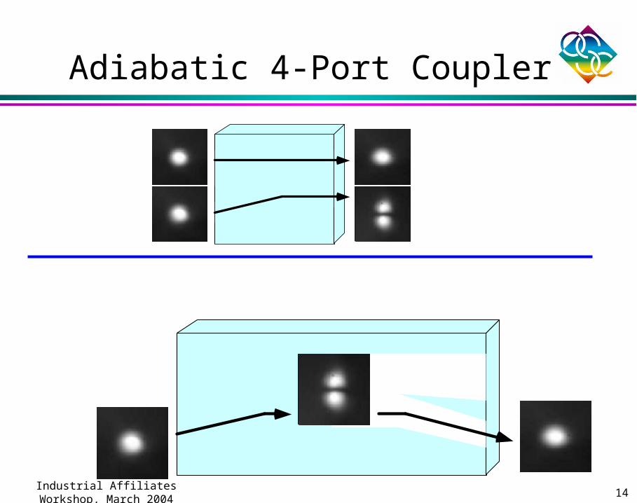
Adiabatic 4-Port Coupler
14

Industrial Affiliates Workshop, March
2004
Add/Drop Performance
• 20 dB Extinction
• 0.4 nm 3 dB Bandwidth
Electron. Lett. 37(13), 2001
1562 1564 1566 1568-20
-15
-10
-5
0
Rel
ativ
e P
ower
(dB
)
Wavelength (nm)
1562 1564 1566 1568-20
-15
-10
-5
0
Rel
ativ
e P
ower
(dB
)Wavelength (nm)
1562 1564 1566 1568-20
-15
-10
-5
0
Rel
ativ
e P
ower
(dB
)
Wavelength (nm)
PASS ADDDROP
Pass
AddDrop
Input
15
Industrial Affiliates Workshop, March
2004
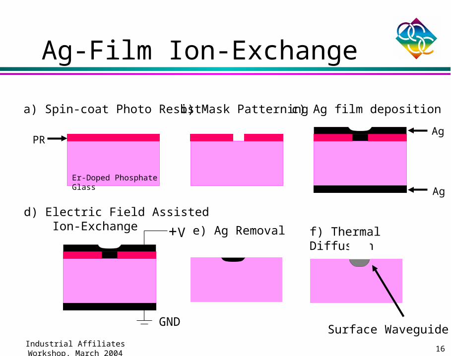
Ag-Film Ion-Exchange
+V
GND
a) Spin-coat Photo Resist b) Mask Patterning c) Ag film deposition
d) Electric Field Assisted Ion-Exchange f) Thermal Diffusione) Ag Removal
PR
Er-Doped Phosphate Glass
Ag
Ag
Surface Waveguide
16

Industrial Affiliates Workshop, March
2004
Pumping with aBroad Area Laser Diode
Erbium/Ytterbium codoped glass
Ion exchanged waveguide
Undoped glass
Single mode waveguide
Multimode section (100 µm)
Dielectric mirror (R>99%)
10 mm 30 mm 10 mm
Surface Relief Bragg grating (R = 72 %)
965 nmpump
Appl. Phys. Lett. 82(9), 2003
17
Industrial Affiliates Workshop, March
2004
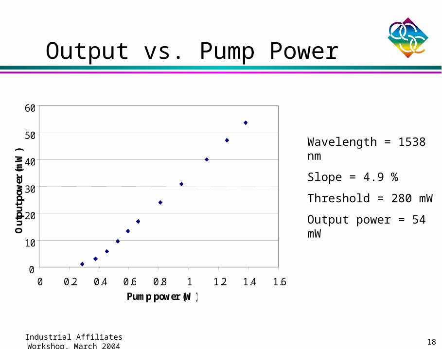
Output vs. Pump Power
0
10
20
30
40
50
60
0 0.2 0.4 0.6 0.8 1 1.2 1.4 1.6
Pump power (W)
Out
put p
ower
(mW
) Wavelength = 1538 nm
Slope = 4.9 %
Threshold = 280 mW
Output power = 54 mW
18

Industrial Affiliates Workshop, March
2004
Outlook
• New device innovations– Mode-locked waveguide lasers– MMI-Waveguide lasers – Tunable dispersion compensators– All-optical header recognition chip
• Exotic host glasses
• Integration with other materials
19
Industrial Affiliates Workshop, March
2004
Conclusion
• Ion-Exchange in Glass
– A Proven Low-Cost Integrated Optics Technology
– Offers Unique Advantages for Various Passive and Active Waveguide Devices
20
Related Documents


