JPL PUBLICATION 77-35 Spacecraft Transformer and Inductor Design [NhSA-CR-l54 104) SPACECRAFT TRANSFOBME0 AND N77-2L3392 INDUCTOR DESIGN (Jet Propulsicr~ Lab.) """ 2 HC Al3/MP A01 CSC Urlclds G3/33 39279 REPRODUClO BY NATIONAL TECHNICAL INFORMA~ION SERVICE U. S. DEPARTMENT OF COMMERCE SPRINQFIELD, VA, 22161 National Aeronautics and Space Administration Jet Propulsion Laboratory California Institute of Technology Pasadena, California 91 103

Welcome message from author
This document is posted to help you gain knowledge. Please leave a comment to let me know what you think about it! Share it to your friends and learn new things together.
Transcript

JPL PUBLICATION 77-35
Spacecraft Transformer and Inductor Design [NhSA-CR-l54 1 0 4 ) S P A C E C R A F T TRANSFOBME0 A N D N77-2L3392
I N D U C T O R D E S I G N (Jet P r o p u l s i c r ~ Lab.) """ 2 HC A l 3 / M P A 0 1 CSC
Urlclds G 3 / 3 3 39279
REPRODUClO BY NATIONAL TECHNICAL INFORMA~ION SERVICE
U. S. DEPARTMENT OF COMMERCE SPRINQFIELD, VA, 22161
National Aeronautics and Space Administration
Jet Propulsion Laboratory California Institute of Technology Pasadena, California 91 103

JPL PUBLICATION 77-35
Spacecraft Transformer and Inductor Design
August 15, 1977
National Aeronautics and Space Administration
Jet Propulsion Laboratory California Institute of Technology Pasadena, California 91 103

PREFACE
The work deecribed in this report was performed by tho Control and
Energy Conversion Division of the Jet Propulsion Laboratory,

ACKNOWLEDGMENT
The author is grateful to Dr. G. W. Wester, S. Nagano, E. L. Sheldon
and Mary F ran Baehler for their aeaistance and suggestions in preparation of
this repor t ,

ABSTRACT
The conversion process i n spacecraft p o s e r electronics requi res the u s e of
magnetic components which frequerrtly a r s the heaviest r i d bulkiest i tems in the
conversion circuit. They a lso h?ve a aignificant effect upon the performance,
weight, cost, and efficiency of the power system. I '
This handbook contains eight chapters , which pertain to magnetic material
selection, t ransformer and inductor design tradeoffs, t ransformer design, iron
core dc inductor design, toroidal powder core inductor design, window utiliza-
tion factors, regulation, and temperature r ise . Relationships a r e given which simplify and standardize the design of t ransformers and the anolysis of the
c i rcu i t s in which they a r e used.
The inter ic t ions of the various design parameters a r e a l so presented in
simplified f o r m ao that tradeoffs and optimizations m a y easily be made.

CONTENTS
CHAPTER I
Figures
1-1
1-2
1-3
1-4
1 -5
1-6 1-7
1-8
r -9 1-10
1 - 1 1
1 -12
MAGNETIC MATERIALS SELECTION FOR STATIC INVERTER AND CONVERTER TRANSFORMERS . * e v e 1.1
Introduction . . . . . . . . . . . . . . . . . . . . . . I . . . . . . . . . . . . . . 1-2
Typical Operation . . . . . . . . . . . . . . . . . . . . . . . . . . . . . . . . . t -2
Material Characteristics . . . # . . . . . 0 # . . . . 4 # . # 0 1 . . 1 1 ~ 1-3
Core Saturation Definition . . . . . . . . . . . . . . . . . . . . . . . . . 1-5
The Teatsetup ................................... 1-9 . . . . . . . . . . . . . . . . . . . . . . . . . . . core Saturation Theory. 1 - 1 5
. . . . . . . . . . . . . . . . . . . . . . . . . . . . . . . . . . . . . . . . . . A i r Gap 1-16 ................................. Effect of Capping 1-16
. . . . . . . . . . . . . . . . . . . . . . The New Core Configuration 1 - 2 5
Summary . . . . . . . . . . . . . . . . . . . . . . . . . . . . . . . . . . . . . . I . 1 - 3 0
Bibliography . . . . . . . . . . . . . . . . . . . . . . . . . . . . . . . I . . . . . 1-31
Magnetic core material characteristics ............. 1-4
Materi rle and constraints ......................... 1-9
. . . . . . . . . . . Comparing B,/B, on uncut and cut coree 1-21
........ Comparing AH.AHOp on uncut and cut cores 1-22
.................................. Composite cores 1-28
.................. Typical driven transistor inverter . . . . . . . . . . . . . . . . . . . . . . . . . . . . Ideal square B-H loop.
The typical B-H loops of magnetic materials . . . . . . . . . . . . . . . . . . . . . . . . . . . . . . . . . . . . . Defining the B-H loop
Excitation current . . . . . . . . . . . . . . . . . . . . . . . . . . . . . . . . . . . . . . . . . . . . . . . . . . . . . . . . . . . . . B-H loop with dc bias
Typical square loop material with ac excitation . . . . . . Dynamic' B-H loop test fixture . . . . . . . . . . . . . . . . . . . . .
. . . . . . . . . . . . . . . . . . . . . . . . Implementing dc unbalance
. . . . . . . . . . . . . . . . . . . . . . . . . . . . . Magnesil ( K ) B-H loop
. . . . . . . . . . . . . . . . . . . . . . . . . . . . . Orthonal (A) B-W loop
. . . . . . . . . . . . . . . . . . . . . . . . . . . . . 48 Alloy (H) B-H loop
Preceding page blank vii

CONTENTS (contd)
Sq, Permailoy (P) B-H loop, . , . . . , , . , . , . , . . . . . Supermalloy (F) B-H loop , . . , . , , . , , , , . . , . . . . , Composite 52029 (2K), (A) , (H), (P), and (F) 3-H loops . , , . , , , . , , , , , , , . , , . , , . , , . Magneail ( K ) B-H loop with and without dc . . . , . . . , . Orthonol ( A ) B-H laop with and without dc , , , , , . , , . 48 Alloy (H) B-H loop with and without dc , , , , . , , . , Sq, Permalloy (P) B-H laop with and without dc , . . , , Supermalloy (F) B-H loop with and without dc , . . . , . , Unmagnetized materid1 , , , . , , . , , , , . , . , . , . . . , . Magnetized mate rial, , , , , . . , . . , . . . . , . . . , , , . . A i r gap increases the effective length of the magnetic path . . . . . . . , . . . . , , , . . , , . , . . . . , . Implementing dc unbalance . , , . , . , , . . . , . , . , , . . Typical cut toroid . , . . . . . , . . , , . . . . , , . . , . . , Typical cut ' 'C1' core . . . . . . . . . , . , . . , . , . . , . , . Magnesil 52029 (2K) B-H loop, (a) uncut and (b) cut . , . , . , . , , . , . . . . , . . . . . . , , , . . . . , Qrthonol 52029 (2A) B-H loop, (a) uncut and (b )cut , , . . . . . l l l . . , . , , I . . I I . I ~ . . I ~ I . . l .
48 Alloy 52029 (2H) B-H loop, (a) uncut and (b )cut . . . l . . . . , . , . , , , . , . , . , . l , , . . . . , l . ,
Sq. Permalloy (2D) B-H loop, (a) uncut and (b )cut , . . . . , . . , l , . . . l . . I . . . . . , . , , , . . . . , Supermalloy 52029 (2F) B-H loop, (a) uncut and ( b ) ~ ~ t , , , , . . ~ . , , ~ . . ~ ~ . ~ ~ ~ ~ ~ , ~ ~ ~ ~ ~ . . ~ ~ ~ ~
Defining AH anci AHOp . . . . . . . . . . . , . . . . . . . . . Inverter inrush current measurement: . . . . . . . . , . , . Typical inrush of an uncut: core in a driven inverter. , . 1-23
Typical inrush current of a cut core in a driven inverter. , , . . . , . . . . . . . . , , . . . . . . . . . . . + . . . 1-23
T - R supply cur rent measurement , . . . . , . . . . , . . . . 1 -24
Typical inrush current of an uncut core operating from an ac source . . . . , . , . . . . , . . . . . + . . . . . . + 1-24
Typical inrush current of a cut core in a T-R. , . . . . , 1-24 - P A M PUNK NQT4 4qtg$\qa viii

CONTENTS (contd)
CHAPTER I1 A
B
C
D
G F
Tables
2 -1
2 -2
2 -3
2 -4
2 - 5
2 -6 2 -7
2-8
2-9 2-10
2-11
Figures
2-1 2 -2
2 -3
2 -4
The uncut core excited at 0 . 2 T/cm . . . . . . . . . . . . Both cores cut and uncut excited at 0 . 2 T J C ~ . . . . . . Cores before assembly. . . . . . . . . . . . . . . . . . . . . Cores after assembly . . . . . . . . . . . . . . . . . . . . . . S t a c k i x l . . . . . . . . . . . . . . . . . . . . . . . . . . . . . Stack one half 1 x I and one half butt stack . . . . . . . . TRANSFORMER DESIGN TRADEOFFS . . . . . . . . . .
. . . . . . . . . . . . . . . . . . . . . . . . . . . . Introduction
The A r e a Product A and Its Relationships . . . . . . . P
Transformer V o l u m e . . . . . . . . . . . . . . . . . . . . . Transformer Weight . . . . . . . . . . . . . . . . . . . . . . . Transformer Surface Area . . . . . . . . . . . . . . . . . . Transformer Current Density . . . . . . . . . . . . . . . .
Core configuration constants . . . . . . . . . . . . . . . . . Powder core characteristics . . . . . . . . . , . . . . . . . Pot core characteristics . . . . . . . . . . . . . . . . . . . . Lamination characteristics . . . . . . . . . . . . . . . . . . C-core characteristics . . . . . . . . . . . . . . . . . . . . . Single-coil C-core characteristics . . . . . . . . . . . . . Tape-wound core characteristics . . . . . . . . . . . . . .
. . . . . . . . . . . . . . . . . . . . . . . . . . . . Conetant Kv Constant Kw . . . . . . . . . . . .. . . . . . . . . . . . . . . . Constant Kg . . . . . . . . . . . . . . . . . . . . . . . . . . . . Constant K . . . . . . . . . . . . . . . . . . . . . . . . . . . .
j
C-core . . . . . . . . . . . . . . . . . . . . . . . . . . . . . . . El lamination . . . . . . . ! . . . . . . . . . . . . . . . . . . .
. . . . . . . . . . . . . . . . . . . . . . . . . . . . . . Pot core
Tape-wound toroidal core . . . . . . . . . . . . . . . . . . .

CONTENTS (contd}
Powder core. . . . . . . , . . , . . . . . . . , , I . . . . , . 2-5
Tape-wound core, powder core, and pot core volume , , , . , . , , , , . . . , , , . , , . , . , , . , , . , . 2-19
EI lamination volume . , . , , . . . . , , . . . . . . . . . , , 2 - 19
C o r e volume , , . . . , . . . . . , . . . . I . , . . . , , . . 2 - 1 9
Single-coil C-core volume . . . . . , . . . , . , . . . , . . 2-19
Volume versus area product AD f o r pot cores . . , . . . 2 - 2 1 5-
Volume versus area product A for powder cores . . . 2-2 1 P
Volume versus area product A for lalninatirrns . , . , 2-22 P
Volume versus area product An fo r C-cures . . . . . . 2-22
Volume versus area product A' for eingle-coil P C - c o r e s . . . * . . . . . . , . , . . . , , . . . , , , . . . . , . , 2-23
Volume versus area product A for tape-wound , 1 +
P t o r o i d ~ . . . . . . . . . . . . . . . . . . . . . . . , . . . . . . , 2-23
Total weight versus area product A for pot cores. . . 2-25 P
Total weight versus area prodrlct A - fo r powder P cores* . , . , . . . . . . . . . . , . . , . , . , . . . . . , . , , . 2-26
Total weight versus area product A for P laminatiol~s , . . , . . . . . , . , , . , . . , , . + . . . . . 2-26
Total weight versus area product A for C-cores . . . 2-27 P
Total weight versus area product A' for P single-coil C-cores , . , . , . . . . . . . . , . , . , . . . . , 2 -27
Total weight versus area product A for tape-wound P toroida . . . . . . . . . . . 2-28
Tape-wound core, powder core, and pot core surface area At . . . . . . . . . . . . . , . . . . . . . . . . . 2-29
Lamination surface area A t . . . . . . . . . . . . . . . . . . 2-29
C-core surface area A t . . . . . . . , . . . . . . . . . . . . 2 - 2 9
Single-coil C-core surface area A t . . . . . . . . . . . . . 2 - 2 9
Surface area versus area product A for pot P cores, . . , , , . . . . . . . , . . . . , . . + , . . . . . . . . . 2 - 3 1
Surface area versus arca product A for powder P cores . . . . . . , . . . . . . . , . . , , . . . . . , . . . . . . . 2-32
Surface area versus area product A for P laminations . . . . . . , . . . . . . , . . , . + . + . . . . , , , 2-32
Surface area versus area product A for C-cores . . . 2-33 P

CONTENTS (contd)
2 -30 Surface a r e a versus area product A for P . . . . . . . . . . . . . . . . . . . . . . . single-coil C-cores
Surface area varsus area product for tape-wound toroids . . . . . . . . . . . . . . . . . . . . . . . I . . . 1 1 . .
2 -32 Current density vernue area product A for a 25O C P . . . . . . . . . . . . . . . . . and 50°C rise for pot cores .
2-33 Current deneity versus a r e a product A fo r a 25°C P . . . . . . . . . . . . . . and 50°C r i se for powder corca
2 -34 Current density versua area product A for 25°C P . . . . . . . . . . . . . . . . and 50°C rise for laminations
2 -3 5 Current density versus a r e a product A for 25°C . . , . . . . . . . . . . . * . and 50°C rise for C-cores
2-36 Current density versus area product A for a 25°C . . . . . . . . . and 50°C rise for single-coil C-cores P. Current denr~ity v e r ~ u e area product A, for 25°C
P . . . . . . . . . . . and 50°C r i se for tape-wound toroida
CHAPTER 111 POWEl3,TRANSFORMER DESIGN t , 1 + , 0 0 * * , 3-1
. . . . . . . . . . . . . . . . . . . . . . . . . . . . A Introduction 3 -3
. . . . . . . . . . . . . . . B The Design Problem Generally 3 -3
Relstionehip of A- to Transforme;. Power Handling Capability . . . . - . . . . . . . . . . . . . . . . . . . . . . . . . 3-5
Output Power vs Input Power vs Apparent Power Capability. . . . . . . . . . . . . . . . . . . . . . . . . . . . . . 3 - 5
A 2.5-kHz Transformer Design Probletn A e An Example . . . . . . . . . . . . . . . . . . . . . . . . . . . . . . 3-9
A 10-kHz Transformer Deeign Problem As An . . . . . . . . . . . . . . . . . . . . . . . . . . . . . . Example 3-20
REFERENCES . . . . . . . . . . . . . . . . . . . . . . . . . . . . . . . . . . . . * 3-28
. . . . . . . . . . A P P E N D I X 3 , A Transformer Power Handling Capability 3-29
Tables . . . . . . . . . . . . . . . . . . . . 3-1 C-core charac ter i s t ics , 3-11
Figures . . . . . . . . . . 3 - 1 Transformer design factnre flow chart 3 -4
Full-wave bridge circuit : . . , . . . . . . . . . . . . . . . . 3 -7
Full-wave, center- tapped circuit . . . . . . . . . . . . . . 347

CONTENTS (contd)
Pus2i.pull. full=wavc. contor-tapped c ircui t . . . . . . . Magnotic material comparison at a constant frequency . . . . . . . . . . . . . . . . . . . . . . . . . . . . . .
CHAPTER IV SZMPLIFZED CUT CORE INDUCTOR DESIGN . . . . . . . . . . . . . . . . . . . . . . . . . . . . . . . . . . Introduction
. . . . . . . . . . . . . . . . . . . . . . . . . . CoreMatc~*ial
Relationship of A to Inductor Energy Idandling Capability . . , . ? . . . . . . . . . . . . . . . . . . . . . . . .
. . . . . . . . . . . . . . . . . . . . . . . . . E Design Example
REFEliENCES . . . . . . . . . . . . . . . . . . . . . . . . . . . . . . . . . . . . . APPENDIX 4. A Linear Reactor Design With an Iron Core . . . . . . . . APPENDIX 4. P C corc and Bobbin Magnetic and Dirnonsional
Specification . . . . . . . . . . . . . . . . . . . . . . . . . . . . Tables
4 - 1
4 . B-1
4 . R - 2
4 . B-3
4 . B-4
4. B-5
4 . B-6
4 . 8 - 7
4 . B-8
4 . B-9 4. R-10
4 . B-11
4 . B- 12
4 . B-13
4 .. B-14
4.B-15
4 . B- 16
4. B-17
. . . . . . . . . . . . . . . . . . . . . . . . Magnetic material
. . . . . . . . . . . . . . . . . . . . . . . . . . I1C1' Core AL-2
t 1 C [ 1 C ~ r ~ A L - 3 . b I . . . . . . . . . . . . . . . . . . . . . . . 14Cf1 Core A L - 5 . . . . . . . . . . . . . . . . . . . . . . . . . . llClr Core A L - 6 . . . . . . . . . . . . . . . . . . . . . . . . . .
. . . . . . . . . . . . . . . . . . . . . . . . l 'C1' Core AL-124
llCrl Core A L - 6 . . . . . . . . . . . . . . . . . . . . . . . . . . llCtl Core A L - 9 . . . . . . . . . . . . . . . . . . . . . . . . . . rrClt Core A L - 1 0 . . . . . . . . . . . . . . . . . . . . . . . . .
. . . . . . . . . . . . . . . . . . . . . . . . . I ICJ1 Core A L - 1 2
. . . . . . . . . . . . . . . . . . . . . . . . j1GIt Core AL-135
I1Cl1 Core A L - 7 8 . . . . . . . . . . . . . . . . . . . . . . . . . (IC0 Core A L - 18 . . . . . . . . . . . . . . . . . . . . . . . . . I ICtt Gore AL-15 . . . . . . . . . . . . . . . . . . . . . . . . .
. . . . . . . . . . . . . . . . . . . . . . . . . l@Clf Garc AL-16
. . . . . . . . . . . . . . . . . . . . . . . . "Ct' Core A L - 1 7
. . . . . . . . . . . . . . . . . . . . . . . . . TICu Core AL-19
. . . . . . . . . . . . . . . . . . . . . . . . . "Ctl Core AL-20

CONTENTS (contd)
Figures
4- 1 4 -2
. . . . . . . . . . . . . . . . . . . . . . . . . 1 1 C r A L - 2 4-39
. . . . . . . . . . . . . . . . . . . . . . . . . I1Ct1 Cora AL-23 4-40
. . . . . . . . . . . . . . . . . . . . . . . . . tlC1l C o r e A L - 2 4 4 - 4 i
. . . . . . . . . . . . . . . . . . . . . . Inductance ve dc bias Flux density versua ldc s A l . . . . . . . . . . , ., . . . . lnc rcase of reactor inductance with flux fringing at the gap . . . . . . . . . . . . . . . . . . . . . . . . . . . . . . Effective permeability of cut core vs permeability of the 1,latarial . . . . . . . . . . . . . . . . . . . . . . . . . . Minimum design permeability . . . . . . . . . . . . . . . . Design curves showing maximum core loss for 2 mil eilicon "C1I cores . . . . . . . . . . . . . . . . . . . I ,
. . . . . . . . . . . . . . . . Wiregraph for "CI1 :-re AL-2
. . . . . . . . . . . . . . . . Wiregraph for t ' ~ : ' l cure ,'.L-3
. . . . . . . . . . . . . . . . . . Wiregraph for core AL-5
Wiregra!;~ . * ' Z a core AL-6 . . . . . . . . . . . . . . . . . . . . . . . . . . . . . . . Wiregra:;? i c f GI1 core AL-124
Wiregraph for I1C" core A L - 8 . . . . . . . . . . . . . . . . . . . . . . . . . . . . . . . . Wiregraph for "GI1 core AL-9
. . . . . . . . . . . . . . . Wiregraph for ItCl1 core A L - 1 0
. . . . . . . . . . . . . . . Wiregraph for IIC1I core A L - 1 2
Wiregraph for I 'Cl1 core AL-135 . . . . . . . . . . . . . . . . . . . . . . . . . . . . . . Wiregraph for i lC1l core AL-7c'
WircgrapI~ for "GIt core A L - 1 8 . . . . . . . . . . . . . . . Wiregraph for I4Cu core A L - 1 5 . . . . . . . . . . . . . . .
. . . . . . . . . . . . . . . Wiregraph for IICtl core AL-16
. . . . . . . . . . . . . . . Wiregraph for I'G" core AL-17
Wiregraph for t lCt ' core AL-19 . . . . . . . . . . . . . . . . . . . . . . . . . . . . . . Wiregraph for l tC" core AL-20
. . . . . . . . . . . . . . . Wiregraph for llC1l core AL-22
. . . . . . . . . . . . . . . Wiregraph for liC" core AL-23
. . . . . . . . . . . . . . . Wiregraph for IiC" core AL-24
CONTENTS (contd)
4. B-21 Graph for inductance, ca, acitance, and .t+actar.ce. , , . . . . . . , . . . , , . , . , . . , . , , . . , .
4. B-22 LIZ Aroa product vs energy T . . . . . . . . . . . , . , , . . CHAPTER V TOROIDAL POWDER CORE SELECTION WlTEI
D C C U R R E N T , , . , . , , . . , , , . . , , , . , , , . , . . , A Introduction , , , , . , , . . . . . , . . . , . . , , , , , ,
Relationship of A to Inductar's Energy Handling P Capability , , . . . . , , . . . . , . . , . . , . , . , , . . ,
C Fundamental Considerations . , . , , , . , , , . . , , . , D A Specified Design Problurrl A s An Example. , . , , .
APPENDlY 5, A Toroid Powder C n r e Selccticn 'Nith DC Current , . . APPENDIX 5, B Magnetic and Dirnensiont~l Spaciiications far
13 Garnmonly U s e $ M ~ l y - : ~ e r l ~ ~ a l l o y Cores , , . . , , Tables
5-1
5 . B-1
Different powder core permeabilities . . . , . . . , , , Dimensional specifications for Magnetic 1nc 55051-A2, Arnold Engineering A-051027-2 , , . . Dimcnaional specifications for Magnetic lac 55121-A2, Arnold Engineering A-266036-2 , . . . . , . . , . . . . , Dimensior.al specifications for Magqetic Inc 55848-A2, Arnold Engineering A-818032-2 . . . . , . , . . , . . , . Dimensional specif ications for Magnetic Inc 55059-A2, A rnold Engineering A - 059043 - 2 . . . . . . . , , . . , . , Dimensional specifications for Magnetic Inc 55894-A2, Arnold Engineering A-8907 5-2 , . . , . . , Dimensional specifications for Magnetic Inc 55071-A2, Arnold Engineering A-291061-2 , . . , . . Dimensional specifications for Magnetic Inc 55586-A2, Arnold Engineering A-345038-2 , . , . . , Dimensional spacifirations for Magnetic Inc 55076-A2, Arnold Enzineering A-076056-2 . , . . . . Dimensional specifict.tions for Magnetic Inc 55083-A?,, Arnold Engineering A-083081 -2 . , , . . . Dimensional specificcztiolls for Magnetic lnc 55439-A2, Arnold Engineering A-759135-2 . . . , . .
x i v aZIOm&.f P.4;; i'b OF FWB Q k J U & Y

CONTENTS (contd)
5. B-11 Dimensional specifications for Magnetic Inc 55110-A2, Arnold Engineering A-488075-2 . , . . , , .
5 . 8 - 1 2 Dimensional specifications for Magnetic Inc 557161A2, Arnold Engineering A-106073-2 , . . , . . .
5. B-13 Dimensional specifications f o r Magnetic Inc 55090-A2, Arnold Engineering A-090086-2 . . . , , , .
Fj :,ure8 5- 1 Flux density versus Idc -t A1 , . . . . . . . . . . . . , . . .
CHAPTER VI
inductance versus dc bias , , . , , . . . . , , , , ,, W i r e and inductance graph for Core 55051 -A2
Wire and inductance graph for Core 55121-A2
W i r e and inductance graph fo r Core 55848-A2
Wire and inductance graph for Core 55059-A2
Wire and inductance graph for Gore 55894-A2
Wire and inductance graph for Core 5507 1 -A2
W i r e and inductance graph f o r Core 55586-A2
Wire and inductance graph for Core 55076-A2
Wire and inductance graph fo r Core 55083-A2
W i r e and inductance graph for Core 55439-A2
Wire and inductance graph for Core 55110-A2
Wire 3nd inductance g raph for Core 55716-A2
W i r e and inductance graph f o r Core 55090-A2
WINDOW UTILIZATION FACTOR KU . . . . . . . . . . . A Int reduction . . . , . . , , , , . . . . , . . , . . . . . . . . . . B Window Utilization Factor . . . . . . . , . , , . . . . . . ,
Conversion Data for Wire Sizes From No. 10 to N 0 . 4 4 l . , . . , l . ~ . . . l . l . . . . . , . , . ~ . . . , , .
D Temperature Correction F? c to r s . , . , . ,. . . . . . . , . E Window Utilization Factor for a Toroid , . . , . . . , . .

7 7 - 3 5
CONTENTS (contd)
Tables
6-1 W i r e t a b l e . . . . . . . . . . . . . . . . . . . . . . . . . . . . . . . . . . . . . . . . . . . . . . . . 6 -2 Layer insulation va AWG
. . . . . . . . . . . . . . . . . . . . . . . . . . 6 -3 Margin vs AWG
. . . . . . . . . . 6-4 A . I . E . E . preferred tape-wound cores
Figures
6-1 Resiotance Correction Factor (I!) for wire resistance at; tempcraturee between -50°C and 100°C . . . . . . . .
. . . . . . . . . . . . . . Computation of mean turn length
. . . . . . . . . . . . . . . . . . . . . . Layer insulated coil
. . . . . . . . . . . Toroid inside diameter versua turns
. . . . . . . . . . . . . Effective winding area of 8 toroid
. . . . . . . . . . . . Wrap tcrroid . . . . . . . . . . . . . . . . . . . . . . . . . . . . . . . . . . . . Periphery insulation
. . . . . . . . . . . . . . . Minimi ~ i n g toroidal inside build
CHAPTER VII TRANSFORMER-INDUCTOR EFFICIENCY. . . . . . . . REGULATION. AND TEMPERATURE RISE
Introduction . . . . . . . . . . . . . . . . . . . . . . . . . . . . . . . . . . . . . . . . . . . . . . . . Transformer Efficiency
Relationship of A to Control of Temperature Rise . . P . . . . . . . . . . . . . . . . . . . . . . 1 Temperature Rise
. . . . . . . . . . . . 2 Calculation of Temperature Rise
3. Temperature Rise Versus Surface Area . . . . . . . . . . . . . . . . . . . . . . . . . Dissipation. . . . . . 4 Surface Area Required for Heat Dissipation
. . . . . . . . . . . Regulation as a Function of Efficiency
. . . . . . . . . . . . . . Designing for a Given Regulation . . . . . . . . . . . . . . . . . . . . . . . 1 Transformers . .
. . . . . . . . . . . . . . . . . . . . . . . . . . . . 2 Inductors
. . . . . . . . . . . . 3 . Transformer Design Example I
. . . . . . . . . . . . . 4 Transformer Design Example I1 . . . . . . . . . . . . . . . . . 5 Lnductor Design Example

CONTENTS (contd)
F Magnetic Core Material Tradeoff. . , , I . , . . I I 4 . . 7 - 32 G Skin E f f ~ c t . , . . . . . , . . . , . . . . . . . . . . . . . . . . 7-43
Reference + . . . . . . . . . . . . . , . . . . 4 ~ ~ . . . . . . . 7-47
APPENDIX 7. A Transformers Deeigned for a Given Regulation, . , . , 7 -48
APPENDIX 7. B Inductore Deeigned for a Given Regulation , . . . . . . . 7-53
APPENDIX 7, C Transformer Area Product and Geometry , . . . , , . . 7 -63
Tables
7-1
7. B-1
7. B-2
7. B-3
7. B-4
7. B-5
7 . C - l
Figures
7 - 1
7 -2
Magnetic core material characteristice. . , . . . , . . . Coefficient K for C cores , , . . , , . . . . . . . . , . .
g Coefficient K for laminations . . . . . . . . . . . . , . . .
g Coefiicient K for pot cores . . . . . . . , . . . . . , . . .
g Coefficient K for powder cores . . . . , . . , . . . . . .
E Coefficient K for tape-wound toroids . . . . . . . . , . .
g Constar*t K relationship. . . . . . . . . . . . . . , , . . .
g
Transformer lose versus output load current , . . . . , Temperature r ise versus surface dissipation , . , . . . Surface area versus area product AD . . . . . . . . . . +
Surface area vereus total watt loss ;or a 25°C and 50°C r ise . . . . . . , . . . . , . . . . . . . . . . . . . . . Transformer circuit diagram . . . . . . . . . . . . . . , . Transformer analytical equivalent , . . . . . . , . . . . . Area product versus regulation . . . . . . . . . . . . . + . Weight versus regulation . . , . . . . . . . . . . . . . . . . The typical dc B-H loops of magnetic material . . . . . Deaign curvea showing maximum core loss for 2 mil silicon. . . . . . . . , , . . . . , , . . , . . . . . . , , . . . . +
Design curves showing maximum core loss for 12 mil silicon.. . . . . . . . . . . . . . . . , . . , . , . . . . . L, . . Deeign curves showing maximum core loss for 2 mil supermendor . . . . . . .,. . , . . . . . , . . . . , . . . . . . Design curves showing maximum core loss for 4 mil supermendor . . . . . . . . . . . . . . . . . . . . . . . . . . .
xvi i

CONTENTS (contd)
Dseign curves showing maximum core los s for 2 m i l 5 0 % N i , 500JaFe . . . . . . . . . , . . . . . . . . . . . 7-39
I.
Design curve8 showing maximum core loss for 2 mil 48% NNi, 52% Fe. . . . . . . . . . . . . . . . . . . . . . 7 -40
Design curves showing maximum Cora lose for . . . . . . . . . . . . . . . . . . . . . . 2mil800JcNi, 20yaFe 7-41
Design curves showing maximum core lose for . . . . . . . . . . . . . . . . . . . . . . . . . . . . . . . f e r r i t e , 7-42
. . . . . . . . . . . . . . . . . Skin depth versus frequency 7-44
Skin depth equal to AWG radius versus frequency . . . 7-45
. . . . . . . . . . . . . Common waveshapee, RMS values 7-46
. . . . . . . . . . . . . . . . . . . . . . Isolation t r ans fo rmer 7 -49
Output induct0 r . . . . . . . . . . . . . . . . . . . . . . . . . . 7 -53
Area product versus core geometry f o r pot co res , , , 7 -65
Area product versus core geometry f o r powder C O T e S . , , . + , . . . , ~ , * , . . . m , . . . . . . ~ n * n . e * . 7 -65
Area product versus core geometry for C cores . . . . 7-66
Area product ve r sus core geometry for laminations . . . . . . . . . . . . . . . . . . . . . . . . . . . . 7-66
Area product ve: i u s core geometry f o r tape-wound . . . . . . . . . . . . . . . . . . . . . . . . . . . . . . toroids 7-67
CHAPTER VIII INDUCTOR DESIGN WITH NO DC FLUX . . . . . . . . . 8- 1
lnt roduction . . . . . . . . . . . . . . . . . . . . . . . . . . . . 8 -2
Relationship of A to Inductor Volt-Ampere P Capability . . . . . . . . . . . . . . . . . . . . . . . . . . . . . 8 -2
Fundamental Considerations . . . . . . . . . . . . . . . . . 8 -3
. . . . . . . . . . . . . . . . . . . . . . . . . D Design Example 8-6 Reference . . . . . . . . . , . . . . I . . . . . . . . . . . . . . 8- 12
Figures
8 - 1 Fringing flux around the gap of an indui tor designed with lamination . . . . . . . . . . . . . . . . . . . . . . . . . . 8-5
xviii

LIST OF SYMBOLS
LY
A C
A P
*t
A W
Aw( B) AWG
33 m
B 8
cir-mil
regulation, Ofo
effective iron area, c m 2
area product, Wa X A=, c m 4
surface area of a transformer, cm 2
wire area, cm 2
bare wire area, cm 2
American Wire Gauge
alternating current flux density, teslas
direct current flux density, teslas
flux density, teslas
flux density to saturate
area of a circle whose diameter = 0 ,001 inches
lamination tongue width, cm
voltage
energy, watt seconds
efficiency
frequency, Hz
fringing flux factor
window height, ern
magnetizing force ampturns/cm
magnetizing force to saturate
current, amps
load current, amps.
primary current, a m p s

LIST OF SYMBOLS (contd)
MLT
secondary current, amps
current deneity, ampe/cm 2
primary current deneity, arnpa/cm 2
secondary current density, amps/cm 2
constant
electrical coefficient
geometry coefficient
gap l o s s coefficient
cur rent density coefficient
\ area product coefficient
surface area coefficient
window utilization factor
volume coefficient '
weight coefficient '
inductance, henry
gap, c m
magnetic path, c m
linear dimension, crn
meter
mean length turn, c m
effective permeability
core material permeability
absolute permeakility
relative permeability

LIST OF SYMBOLS (contd)
turns
power, watts
flux weber s
copper loss, watts
core loss , watts
input power; watts
ou+ut power, watts
heat flux density, watts /cm 2
primary loss, watts
secondary loss , watts
total loss (core and capper), watts
apparent power, watts
resistance, ohms
resistivity
equivalent core- lass (shunt) resistance, o h m s
copper resistance, ohms
load resistance, ohms
primary resistance, ohms
secondary resistance, ohma
total resistance, ohms
conductor arealwire area
wound arealusable window
usable window arealwindow area
xxi

LIST OF SYMBOLS (contd)
S4 usable window arealuaable window area t insulation area
T flux density, teslae
v0 load voltage, volts
Vol volume, c m 3
window area, c m 2 Wa
weight, grams
I: zeta resistance correctiol~ factor for temperature

CHAPTER I
MAGNETIC MATERIALS SELECTION FOR STATIC
INVERTER AND CONVERTER TRANSFORMERS

A . INTRODUCTION
Trans fo rmar s used in s ta t i c i nve r t e r s , converters and t r ans fo rmer - r ec t i f i e r (T-R) supplics intended f o r pace craft pawor applicatione arc
usually of squa re loop tape toroidal design. The des ign of re l iable , efficient,
and lightweight devices far thia use has been seriolaoly hampered by the lack
of engineering data d e ~ c r i b i n g the behavior of both the coxllmonly used and
the more exotic col9c materials with higher frequency equare wave excitation,
A prog ram has been c a r r i e d out at JPL to develop this data from
measu remen t s of the dynamic B-H loop characteristics of the dif ferent tape
core mater ia l s presently avai lable from various industry sources . C o r e s were procured in both toroidal and "Cit forms and w e r e tes ted in both
upgappod (uncut) and gapped (cut) configuratione, Tho following descr ibea
the results of th is investigation.
B. TYPICAL OPERATION
Transformers used for inver te re , conver te rs , and T-R suppl ies
operate f rom the spacecraft power bus, which could be dc or ac. In some
power applications, a commonly used circuit is a driven transistor switch
arrangement such as that shown in Fig. 1-1,
Fig. 1 - 1, Typical dr iven t r ans i s tor i nve r t e r

One i.mportant conrideral!.on affecting the deeign of euitabie t ran8 - formers ia that care must be taken to ensure that aperatlon involves
balanced dr ive to the t ransformer primary. In the absence of balanced
drive, a net dc current will flow In the t ransformer pr imary, which causes
the core to sa tura te easily during alternate half-cycles. A saturated co re
cannot ltlupport the applied voltage, and, because of lowered t ransformer
Impedance, the current flowing in a ewitching transistor Le limited mainly by
i ts beta, The resulting high current, in conjunction with the t ransformer
leakage inductance, resulte in a high voltage sp ike during the ewitching
sequence that could be destructive to the t rans ia ta rs . T o provide balanced
drive, it is necessary to exactly match the t r a m i s t o r s for VCE (SAT) and
beta, and thlr. Ls not always sufficiently effective, Also, exact matching
of the t rans is tors irr a major problem in the practical senae.
MATERIAL CHARACTERISTICS
Many available ca re mater ial8 approximate the ideal square loop
character is t ic illuetrated by the 8-H curve shown i n Fig. 1-2.
Fig. 1-2, Ideal square B-H loop
Representative d c B-H loops for commonly available core mater ia l s
are shown in Fig. 1 - 3 , Other charac ter i s t ics are tabulated in Table 1-1.
Many a r t i c l e s have been written about inverter and converter
t ransformer design. Usually, the author's recommendation represents a
compromise among mater ial character is t ics such as those tabulated in

I I , amp-turn/cnl
Fig. 1 - 3 . The typical dc B-M loops of magnetic materials
Table 1-1, Magnetic core material characteristics
Loss factor a t 3 kHz and 0 . 5 T, W / ~ I
33, 1
17,66
11 .03
5.51;
3 .75
Saturntcd DC coercive Mater ial
don&Y, 3 ratio deqsity, q c m 3
'1 T = lo4 Gauee
21 p/cm3 = 0.036 ~ b / i n . ~ .-
Magncril Sllectrun Microail Suparmfl
Deltamu Orthonol 49 Sq. Mu
Allegheny 4750 48 Alloy 7arpenter 49
4-79 Permalloy Sq. Permal loy 80 Sq. Mu 79
Supamalloy
3% si 97% FC
50% Ni 50% Fa
48% Ni 52% Fa
79% NI 17% Fa 4% Mo
78% Ni 17% Fe
5% MO
1 . 5 - 1 . 8
1.4-1.6
1 .15-1 .4
0. 66-0.82
0 .65-0 .82
0.5-0.75
0.125-0.25
0.062-0.187
0.025-0,05
O.O(r37-0.01
0 .85-1 .0
0.94-1.0
0.80-0.92
0 .80-1 .0
0.40-0.70
-- 7.63
8.24
8 . 1 9
8.73
8.76

Tablc 1 - I and displayed i n Fig, 1 - 3. Thibsu data arc typical of commc rcially
available core materiala that a r c auitoblc for thc particular application,
A s can be sccn, the material that provides the highcat f l u density
{si l icon) would result in smal lest component s i z c , illnd t h i s would inflncncc?
the choice, if e ize were the most important c neideration, The type
78 material ( s e e the 78% curvc in Fig. 1 - 3 ) has thc laweal: flux denrrity. This
results in the largest e i z e transformer, but , on the other hand, this
material has tho lowest coercive force and thc loweet core lone of any
core material available,
U ~ u a l l y , inverter transformer design i e aimed at the smallest s izc ,
with the highest efficiency, and adequate performance under the wideat
range of environmental conditions, Unfortunately, the core material that
can produce the smallest s i z e has the loweat efficiency. The highest
efficiency matartala result In the largcat s ize . Thue the t rane farmer
designer must make tradcofts betwccn allowabir; transformer size and the
minimum efficiency that can be toleraied. The choice of core material wi l l then be based upon achieving the best characterist ic on the most
cr i t ical or important design parameter, and acceptable compromises on thr: other parameters,
Based upon analysis of a number of designs , most engineers select s ize
rather than efficiency as the most important criteria and select an inter - mediate loss factor core niaterial for their transformers. Consequently,
square loop 50 -50 nickel-iron has become tho most popular inaterial.
D. CORE SATURATION DEFINITION
To standardize the def in i t ion of r;aturatiord several unique points
on the B - H loop are defined as shown in Fig. 1 - 4 .
The straight Line through (Ho, 0) and (Hg, Bs) may be written as:

Fig, 1-4. Defining the B-H loop
I t I I
-*-
1XClICD MINOR LOOP
The llne through (0. Bg) and (H B 1 has es sent ia l l y z e r o elope and may be 6 ' s
written as:
0
Equations ( I ) and ( 2 ) together defined "aaturationl' conditions as follows:
I I
Solving Eq. ( I - 3 ) for H,,
"g,, 11,
I
where
by definition,

4
B A
h v
SATMAT ION OCCURS WHEN 0 = 2A
Fig. 1 - 5. Excitation cuyrcnt
Saturation o c c u r 6 by aefinition is when the peak exciting current is twice thc
average cxciting cur ren t as shown in Fig , 1 - 5 , Analytically this nlcans that;:
Solving Eq, (1 - 1 ) fo 1 F , we obtain
T o obtain the presaturation d c margin (AH), Eq. (1 - 4 ) is ~ u b t r a c t c d from
E q . (1 - 3 ) :
The actual unbalanced dc current must be limited to
< AH1
'dc = N " (amperes)
w h e r e
N = TURNS
1 = mean magnetic length rn


E. THE TEST SETUP
A test fixture, schematically indicated in Fig, 1 - 8 , was built l o cffcct
c o m p a r i ~ o n of dynamic B-H loop c h a r a c t e r i s t i c s of v a r i o u s core materiala,
Corcs w e r e fabricated from various care materiale In the basic core con-
figuration designated No. 52029 for toroidal cores manufactured by
Magnet ics , Inc, The materials used were thuae most likely to be of in teres t
t o designers of inverter or converter traneformere, Test conditions are
l i s ted i n Table 1 - 2 .
I 1 VERT TEKTRONlX
POWER @--rEzf-7 OSCILLATOR I TRANS- I
] FORMER I /-
p ~ " . B CURRENT 536
PROBE HOR 1 Z
QE POOQ l,&NplW'if
2.4 k t b
Fig. 1 Dynamic l3-H loop test fixtu1.e
1
I I 1
5 1
Table 1-2 . Materials and t e s t condit ions
SQUARE WAVE I t I $~oknl I I 7 t
Coro type
52029 (2A)
52029 (2D)
52029 ( 2 F)
52029 (2H)
52029 (2H)
I I
0.7; I I
PF I I I
I I l - l l l - - ~ a
I GND OSCILLOSCOPE
_i f i I U
- ==
9 . 4 7
9.47
9. 47
9 .47
9 . 47
Material
Orthonol
Sq. Permalloy
Supermalloy
48-Alloy
Magnesil
N~
5 4
54
5 4
5 4
54
-
Bm, T
1 . 4 5
0. 75
0. 75
1. 1 5
1 . 6
Frequency, k H z
2. 4
2. 4
2. 4
2. 4
2. 4


'F, CORE SATURATION THEORY
The domain theory of the nature of magnetism is based on the
assumption that a l l magnetic' mater ia l s consist of individual molecular
magnets. These minute magnets a r e capable of movement wi th in the
mate r i a l , When a magnetic ma te r i a l is in i ts unrnagnetized s ta te , the
individual magnetic particles a r c arranged a t random, and effectively
neutral ize each other. An example of this i~ shown in Fig. 1 -21, where the
t iny magnet ic particles a r e arranged in a disorganized manner , The north poles a r e represented by the darkened ends of the magnetic particles.
When a ma te r i a l is magnetized, the individual par t ic les a r e aligned o r or ien ted in a definite direction (Fig. 1-22),
Fig. 1-21. Unmagnetized ma te r i a l Fig. 1 -22. Magnetized ma te r i a l
The degree of mag~zetization of a ma te r i a l depends on the degree of
alignment of the particles. The external magnetizing force can continue
up t o the point of saturation, that is , the point a t which essent ia l ly a l l of
the domains a r e 1inr.d up in the same direction,
- 6 In a typical toroid core, the effective a i r g a p i s less than 10 cm.
Such a gap is negligible in comparison t o the r a t i o of mean length to
permeability. If the toroid were subjected to a strong magnetic field
(enough to sa tura te ) , essen t ia l lya l l of the domains would tine up in the
same direction,

If suddenly the field w e r e removed a t Bm, the domains would remain
l ined up and be magnetized along that axis. The amount of flux density that
remains is called res idual flux or Br. The r e su l t of th is effect was shown ea r l i e r in F igs . 1-16 to 1-20.
G. AIR GAP
A n air gap introduced into the core has a powerful demagnetizing
effect , result ing in "shearing ove r f i of t h e hys te res i s loop and a consider-
able decrease in permeabil i ty of high-permeability ma te r i a l s . The dc
excitation follows the s a m e pat tern , However, the core bias is cons ider -
ab ly l e s s affected by the introduction of a s m a l l air gap than the magneti-
zation charac te r i s t i cs . The magnitude of the air gap effect a leo depends
on the length of the mean inagnetic path and on the cha rac t e r i s t i c s of thz
uncut core. F o r the sa6ne air gap, the decrease i n permeabi l i ty will b e
l e s s with a g r e a t e r magnetic flux path but m o r e pronounced i n a low
coerc ive force , high-permeability core .
H I E F F E C T O F GAPPING
Figure 1-23 shows a comparison of a typical to ro id core B - H loop
without and with a gap. The gap inc rease s the effective length of the
magnetic path. W h e n voltage E is impressed a c r o s s p r i m a r y winding N I of a t r ans fo rmer , the result ing cur ren t i, will be smal l because of the
highly inductive circuit shown i n F ig . 1-24. For a pa r t i cu l a r a ize core,
n~axinium inductance occurs when the a i r gap i s minimum.
When S 1 i s closed, an unbalanced dc cu r r en t flows in the N 2 tu rns and
the core i s subjected to a dc magnetizing force, resul t ing in a flux density
tha t m a y be expressed as
[ tes las ] (1-11)

WITHOUT GAP A
WITH GAP 0
F i g , 1-23 . A i r gap i~ lcrcases the cffcctivc length of the magne t i c path
Fig . 1 - 24. Implenlenting dc unbalance
In converter and i n v e r t e r des ign , th is is augmented by the ac flux
swing, which is:
[ teslas] (1 -12)
If the s u m of Bdc and Bac shifts operation above the m a x i m u m o p e r a t -
ing flux densi ty of the core material, the incremental permeability ( ~ a c ) is
reduced. This lowers the impedance and increases the flow of magnet iz ing


Table 1-4. Comparing AM-AHOp on uncut and cut cores
A direct comparison of cut and uncut cores was made electrically
Matcrlal
Ortllonal
4 8 Alloy
Sq, Pcrmalloy
Supcrmalloy
Magnesil
by means of two different test c ircui ts . The magnet ic material used in this
branch of the test was Orthonol, The operating frequency was 2 . 4 kHz, and
the flux density was 0.6 T. The first teat circuit, sliown in Fig. 1 - 3 3 , was
Bm* (tcsla)
1 , 41
1 . 1 2
0, 73
0. 6 8
1, 54
a driven inverter operating into a 30 W load, with t!le transistors operating
into and out of saturation, Drive was applied continuously. Sl controls tile
Bat (tesla)
1. 1s
0, 89
0, 58
0. 58
1. 23
supply voltage to Ql and QZ. b
2.4 kHz SQUARE
amp- turn/cm
W
PRO BE
13dc' (tcsla)
0. 288
0. 224
0. I46
0.136
0, 31
Fig. 1 - 33, Invarte r inrush current measurement
Uncut cu t
0.0125
0, 0250
0. 01
0. 0175
0.075
AH^^
0 . 8 9 5
1,150
0 , 9 8 3
0.491
7 . 1 5
AH
0. 0
0. 0
0. 005
0, 005
0 . 0 2 5
A r-I
0. 178
0,350
0. 178
0 , 224
1 . 7 8


A s n ~ a l l amount of air gap, l ee s than 25 Fm, has a powerful effect on
the demagnetizing force and this gap has li t t le effect on core loss . This arnall
amount of a i r gap decreases the residual magr~et ism by 'lahearing over" the
hysteresis loop. This eliminated the problem of the core tending to remain
eaturated.
A typical example skrrwing the meri t of the cut core w a s in the eheck-
out of a Mariner spacecraft. During the checkout of a prototype science
package, a large ( 8 A, 200 ps} turn-on transient w a s obeervcd. The normal
running current was 0. 06 A , and wae fused with a parallel-redundant 1/8-A
fuse as required by the Mariner mar^ 1971 design philosophy, With this
&-A inrush current , the 1/8-A fuses: were easily blown. This did not happen on every turn-on, but only when the core would Itlatch upi' in the %rang
direction for turn-on, Upon inspection, the t ransformer turned out to be
a 50-50 Ni-Fe toroid, The design was changed from a toroidal core t o a
cut-core with a 25-pm ai r gap, The new design was completely successful
in eliminating the 8-A turn-on transient,
A NEW CORE CONFIGURATION
A new configuration has been developed f o r t ransformers which combines the
protective feature of a gapped core with the much lower magnetizing current
requirement of a n uncut core. The uncut co re functions under normal oper-
ating conditions, and the cut co re takes over during abnormal conditions to
prevent high switching transients and their potentially destructive effect orn
the t ransis tors ,
This configuration is a composite of cut and uncut cores assembled togethe;
in concentric relationship, with the uncut core nested within the cut core, The
uncut core has high permeability and thus requires a very small magnetizing
current. On the other hand, the cut core has a low permeability and thus
requires a much higher magnetization current .
The uncut c o r e is designed to operate a t a flux density which is sufficient for
normal operation of the converter. The uncut co re may saturate under the
abnormal conditions previously described. The cut core then takes over and
supports the applied voltage so that excessive current does not flow. In a


Table 1 - 5 compiles a list of composite core B manufactured by Magnetic8
Inc. , along side their standard dimensional equivalent cores, Also included in
Table 1-5 i s the cores ' area product A which i s described in Chapter 2 . P'
Table 1-5. Compoaitc cores
A cm 4 P'
0.0728
0.144
0.285
0.389
0 .439
0,. 603
1.090
1.455
2.180
2 . 9 1 0
4,676
5.255
7.13
Composite
01605-2D
01 754-21)
01755-2D
01609-2D
01756-20
01606-ZD
01 757-21)
0 t 758-2D
01607-2D
01759-2D
01608-2D
01623-2D
01624-213
A c 66 % Square Permalloy 4/79,
A c = 33% Orthonol 5 0 / 5 0 .
l g = 2 mil Kaption.
Standard
52000
52002
52076
5206 1
52106
52094
52029
52032
52026
52038
52035
52425
52169


J* SUMMARY
Low-loss tape-wound toroidal core materials that have a very square
hyatereaie characteristic (B-H loop) have been uaed extenrrively in the design
of spacecraft tranaformere, Due to the squarsneee of the B-H loops of theec
materials, tratssformers designed with them tend to saturate quite easily,
As a result, large voltage and current epikes, which cause undue trees on
the electronic circuitry, can uccur. Saturation occurs when there i s any
unbalance in the ac drive to the traneformer, or when a n y dc excitation
exists. Also, due to the square characteristic, a high residual flux state
(8,) m a y remain when excitation i s removed. Reapplicatioil of excitation i n
the same direction may cause deep saturation and a n extremely large cur-
r e n t spike, limited only by source impedance and transformer winding
resistance, can result. This can produce catastrophic failure.
By introducing a ernall (less than 25-pm) air gap into the ccre, the
problems described above can be avoided and, at the same time, the low-
loss properties of the materials retained. The air gap has the effect of
"shearing over" the B-H loop of t h e material such that the residual flux
state is low and the margin between operating flux density and saturation
flux density is high. The air gap thus has a powerful demagnetizing effect
upon the square loop materials. Properly designed transformers using
'Tcutqt toroid or " C - ~ o r e ~ ~ square loop materials will not saturatt Jpon
turn-on and can tolerate a certain amount of unbalanced drive or dc
excitation.
It should be emphasized, however, that because of the nature of the
material and the small size of the gap, extreme care and control muat be
taken in performing the gapping operation, otherwise the desired shearing
effect will not be achieved and the low-loss properties will be lost. he cores must be very carefully cut, lapped, and etched to provide ernooth,
residue-free surfaces, Reassembly must be performed with equal care.

BIBLIOGRAPHY
Brown, A. A , , et a l , , Cyclic and Constant Temperature Aging Effects on Magnetic Materials for lnvertera and Converters, NASA CR-(L-80001). National Aeronaut ics and Space Administration, Washington, June 1969,
Design Manual Featuring Tapc Wound Cares , - TWC-300, Magnetic Inc, , But lor, Pa. , 1962,
Frost, l2, M+ , ot al . + Evaluation of Magnetic Mater ia l s for Static Invertera and Convcr tcr s , NASA Gli-1226. National Aeronautics and Space A d m i n i s - tration, Waehington, February 1969.
Lee, R, , Electronic T ransforiners and Circuits , Second Edition, John Wiley & Sons, N e w York, 1958.
Nordonbcrg, H, M . , Electronic Transformers . Reinhold Publishing G o , , New Yark, 1964.
Platt, S., Magnetic Amplif iers: Theory and Application, Pi4cntice-Hall , Englewood k l i f i a , N. J. , 1958.
Flight Projects , Space Programs S u m m a r y 37-64, Voi. I, p. 17, Jct Propulsion Laboratory, Pasadena, Calif . , Tuly 3 1, 1970.
Techn ica l Data on Arnold Tape-Wound Cores, TG-101A. Arnold Enginear- ing, Marengo, I l l . , 1960.

CHAPTER LI
TRANSFORMER DESIGN TRADEOFFS

Manufacturors have for years assigncd numeric codes to their corcs ;
thee c codes repr cscnt the power -11andling ability. This mctl~ocl as signs to oacll
c o r e a numbor which is tho product of i ts window area (W,) and co re c r o s s
section area (Ac) and is called "Arca Product, " Ap.
Theee numbers are used by core suppliers to surr~marize dimensional
and electrical properties in their catalogs. They are available fcr lamina-
tions, C-cores, pot cores, powder cores, and toroidal tape-wounri cores .
The author has developed additional relat ionsl~ips between tht? Ap nutnbers
and current d c ~ ~ ; i t y 3 for a given regulation and temperature r i se . The a rea 4
product A is a dimension to the fourth power P , whereas volume i s a dimen- P
s ion to the third power i 3 and surface area A t is a dimension to the second 2 power 1 . Straight-line relationships have been developed for A and volumc,
P A and surface a r e a A and A and weight .
P t ' P These relationships can now be used as new tools to simplify and stan-
dardize t1.c process of transformer design. They make i t possible to design
t ransformers of lighter weight and smal le r volume o r to optimize efficiency
without going through a cut and t r y design procedure. While developed specifi-
cally for aerospace applications, tV,e information has wider utility and can bo
usad for the design of non-aerospace t ransformers as wall.
Because of i t s significance, th a r e a product A is t reated extensively, P
A great deal of other information :s also presented for the convenience of
the designer. Much of the mater ia l i s in graphical o r tabular forin to assis t
the designer in making the tradeoffs bes t suited for his particular applicat ion
i n a minimum amount of time.
Precedin~ page blank

Be THE AREA PRODUCT A AND ITS RELATIONSTIIPS P
The A of a core i s the product of the available window arca Wa of rhc P 2 corc in squarc ccnt imctcrs (cm ) multiplied by the effective cross - sectional
2 arca Ac in squarc ccntirnctcra (crn ) which may be stated a s
Figurea 2 - 1 - 2 - 5 show in outline fosm five transformer corr! typos that
are typical of those shown in the catalogs of suppliers.
There i s a unique relationship between the arcla prorl~rct A c11at.actci.istic P
number for transformer coves and several other itilportant: pa ramc tc r s which
must be considered in transformer design.
Table 2 - 1 was d ~ v e l o p e d using the least-squares cul-vc f i t I ' r ~ ~ r n tho data
obtained in Tables 2 - 2 through 2 - 7 . The area product A re la t ionships with P
volume, aurface area, current density, and wcight for pot: corcu, p o w c l e ~
cores, laminations, C-cores, and tape-wound cores wi l l bc prescn tcd i n dctail
i n the following paragraphs.
Table 2-1. Core configuration constants 1
l< v
14 , .5
13. 1
1q.7
17.[1
25. G
25,O
5 K.A(X) A , = K A 0.50 J P " P
W t = K A 0,75 Vol = K A 0.75 W P V P
K~
3 3 . 8
3 2 . 5
4L.3
3 9 . 2
44.5
5 0 , 9 I
(x)
- 0 . 17
-0, 12
-0.12
-0. 14
-0.14
-0. 13
Core
Pot core
Powder core
Lamina tion
C -core
Single-coil
Tape -wound core
Kw
48.0
58, 8
6 8 . 2
66.6
76 .6
8 2 . 3
K . ( 5 0 ' ~ )
6 3 2
590
5 34
468
569
3 6 5
Losses
u= 'fe
Pcu >>Pfe
Pcu= Pfc
Pcu'Pfe
Pcu>>Pfe - u- 'fe
K * (25'~)
4 3 3
403
366
3 2 3
395
250

Fig . 2-1 , C-core
Fig , 2- 2, EI lamination
Fig. 2-4. Tape-wound
Fig. 2 - 3 . Pat core
E'ig. 2 - 5, Powde
t o ro ida l core
*c
1- core

Definitions for Table 2-2
Information given is listed by column as:
Manufacturer part number
Surface area calculated from Figure 2-22
Area product effective iron. area times window area
Mean length turn
Total number of turns and wire size using n w;ldow utilization factor K = 0.40 U
Resistance of the wire at 50°C
Watts loss is based on Figure 7-2 for a AT of 25°C with a room ambient of 25°C surface
dissipation times the transki-rnrr surface area. total loss is PcU
Current calculated from column 6 and 7
Current density calculated from column 5 and 8
Resistance of the wire at 75" C
Watts loss i s based on Figure 7-2 for a AT of 50°C with a room ambient of 25'C surface
dissipation times the transformer surface area, total loss is PcU
Current calculated from column 10 and 11
Current density calculated from column 5 and 12
Effective c-re weight for silicon plus copper weight in grams
Transforn~or volume calculated from Figure 2-6 C. _, 'fective cross- section

Table 2-2. Powder core characteristics -
1
2
3
+ 5
6
7
a
1
Core
55051
55121
J5.%8
55059
558?4
55586
55071
55076
5 1 55083
[; 55090
55439
55716
5 5 l l a
2
2t err.'
7.19
12.3
17.3
21.9
30.
48.6
44.7
51.6
copper lossxi-iron lorn
66.a
8%4
86.9
100.0
124.0
7
PZ
0.216
0.369
0.519
0.657
0.924
1.46
I. 34
I. 55
3
A crri ?
0.0-137
0.137
0.254
0.*"5
1.021
1 . U t
1.466
2.46
2.CQ
2. bB
2.60
3, OD
3-72
B
Isv
1-00
0.E48
0.761
0.719
0.703
0,558
0.602
0.574
4.57
6.1-
8.48
9.38
13.66
9
AT ZS'C
,= I,wnz
637
522
t69
443
433
3 44
37 1
3 53
0.541
0.198
3- 553
0. ;a0
0.457
4 5 6
?.%T crn P B 50.C
1 D 11 I2 13 14 1 15 16
J I 1lcmZ It Cs - 5.L36 0.503 1-46 644 9.1 2-71 1.39 n.113
333
3 07
3 61
296
zaz
2. IL
0.563
0.3.5
1- 39
2-126
5-15
4.07
5.17
7.50
11.9
9.32
14.3
19.6
6.84
10.8 1
8 - 4 9
13.0
17.8
6.02
6.65
7-58
6-54
7.09
86 2S
D.Bb1
1.211
1.533
2.14
3.40
3.13
3.61
4-60
6.26
6.08
7.00
8, be
95,. 2E
1372 25
9 5 q Z 5
1684 z5
2125 t S
0-215
0.51 3
0.897
1.27
1-81
4.69
5-70
4.71
2.71 14o 2 j
L 91 1 L57 t S
762 1::: I be3
0.790
0.72a
0.807
0-699
0.665
3.z4
:. 51
6-39
4 -73
4.88
6.8 6.3
10 11.3
16 16.3
36 23.2
35 59-9
4; 7
5: 61.0
a2 R6.0
1 3 1 140
1CZ i 0 P
1 3 3 1 7 0
176 226
1-05
1. GZ
0.812
0.877
0.814
497
449
9 3
431
410
3:6 25
351 z5
902 25
656 z j
6 1 5 2 5
6 t f
63:
500
540
516
3.11
5.07 I 1::::
34.1
59.5
5 P 1
69-0
93.4
7.28
I h 4
23.3
21.0
25.7
1.06
1-12
I. 95
1.24
I. 44
0.327
0.639
0.458
O.€tb
0.670

Definitions for Table 2- 3
Information given is listed by column as:
Manufacturer part number
Surface area calculated from Figure 2-22
Area product effective iron a rea times window area
Mean length turn
Total number of turns and wire size using a window utilization kctor \ = 0.40
Resistance of the wire at 50°C
Watts loss is based on Figure 7-2 for a AT of 25°C with a room ambient of 25°C surface
dissipation times the transformer surface area, total loss is equal to 2 PcU
Current calculated from column 6 and 7 Current density calculated from column 5 and 8
Resistance of the wire at 75°C
Watts l o s s i s based on Figure 7-2 for a AT of 50°C with a room ambient of 25°C surface
dissipation times the t ransformer surface area, total loss is equal to 2 PcU
Current calculated from column 10 and L 1
Current density calculated from column 5 and 12
Effective core weight for silicon plus cop+er weight in grams
Transformer volume calculated from Figure 2-6
Core effective cross- section

Table 2 -3. Pot core characteristics
copper lass = iron l o s ~ i
9 10 11 12 13 14 15 16
n a75.c P, AT 5O.C Unghl
J = I / - ~ fe cu J = 1/cmZ
1044 D.192 0.230 9.774 1527 0.8 0.32 0.367 0.10
904 0.339 0.304 0.670 1322. 1.7 0.38 0.662 a 1 b
I M B 3.2 0.98 1.35 I 0.25
584 Z. 12 0.791 0.432 853 6.0 2.37 2.78 0.43
2
2.93
4.35
6.96
11-3
17.0
23.9
32.8
44.8
76.0
122,O
1
2
3
4
5
6
1
8
9
10
a
=
0.529
0.458
0.363
0.296
0.271
0.578
D.693
0.639
0.547
0.459
1
9 x 5
1 1 x 7
1 4 x 8
1 8 x 11
2 2 x 1 3
2 6 x 1 6
3 0 x 1 9
26 X 22
47xLB
5 9 x 5 6
535
179
427
344
337
283
3 t 4
1,190
1-67
2.30
3- !4
5-32
8.54
3.80
0.650
1.12
1-79
4.18
9.50
5
cm4 P
0.0065
0.C152
0.0393
0.114
0.246
0.498
1.016
i.01
5.62
13.4
rarT cm
1.85
2.2
2.8
3.56
4.4
5.2
6.0
7.3
9.3
2 0
0.396
1.13
1-01
0.937
0,798 -
0.670
6 7
782
696
6 2
577
492
413
Pz
0.098
0.130
0.208
0.339
0.510
0.717
0.984
1.34
2.28
3.66
&I Q e
25
37 30
74
143
207 30
96 2S
134 25
1B9t5
345 25
6OBZ5
I 3 4.30
21 7-5
36 12.9
5 - 20.8
123 48.0
270 109
L 175
0.309
0.787
1.934
3.46
0.592
1.024
1.636
3.81
8.65
5.17
6.65
13.9
22.0
48.6
98.3
0.63
0. 94
I. 36
h Of
3.12
4.85

Definiticns for Table 2-4
Information given is listed by column as:
Manufacturer part number
Surface area calculated from Figure 2-23
Area product effective iron area times window area
Mean length turn on one bobbin
Total number of turns and wire size for one bobbin using a window utilization factor K = 0.40 U
Resistance of the wire at 50" C
Watts loss is based on Figure 7-2 for a AT of 25°C with a room ambient of 25°C surface
dissipation times the transformer surface area, total loss is equal to 2 PcU
Current calculated from column 6 and 7
Current density calculated from column 5 and 8
Resistance of the wire at 75°C
Watts loss is based on Figure 7-2 for a AT of 50°C with a room ambient of 25*C surface
dissipation times the transformer surface area, total loss is equal to 2 Pcu
Current calculated from column 10 and 11
Current density calculated from column 5 and 12
Effective core weight for silicon plus copper weight in grams
Transformer volume calculated from Figure 2-7
Core effective cross- section (thickness, 0.014) square stack

Table 2 -4. Lamination. characteristics
7
P.
0.123
0.199
0.432
0.71-3
1.22
1 4 3
1.73
1.98
2.70
3.90
5-20
6.90
a. 76
10.8
13.0
15.5
21.1
23.3
32.8
11
rr
0.288
0.464
1-01
I. 67
2-84
3.31
4-04
4-62
6.30
9.10
12.3
116.1
20-4
25- 3
30.1
36.3
49.3
54- 5
76.5
1
2
3
4
5
6
7
8
9
li)
1 1
12
1 3
I 4
15
16
17
l a
19
copper
15
tr*bmr
un 3
0.691
1.35
4 3 4
4.22
19.1
25.3
36.B
39.2
60.0
1 .
164-0
246.0
350.0
481.0
629.0
829.0
1312.0
1654.0
28'5.0
2
4 c d
4-11
6.63
14.4
23.8
40.6
47.7
57-5
66.0
90.0
130-0
176.0
230.0
292.0
361.0
132.0
518.0
704.0
778.0
1093.0
lass
1
Core
EE-3031
EE-2829
El-187
EE-2425
EE-Z6Z7
El-375
81-50
El-21
El-625
El-75
EI-67
El-100
EI-112
El-125
El-138
El-150
El-175
EI-36
El -19
lo.@ r iron
8 7
W I=,/:
0.323
0.276
0.237
0.192
0-602
0.51%
O.6L5
0.514
0.505
1-54
1-40
1.29
1-23
1.15
1.10
1.05
1.034
0.836
0.696
16
2 Ac - 0.0502
0.0907
O.2M
0.'63
O-6lb
0.816
1-15
1-45
2-27
3-27
4.45
5-61
7-34
9.07
11+6
13-1
17-s
15.3
$7-8
12
0.472
0.403
0.347
0.281
0.Bfb
0.762
0.912
C.793
0.737
2.14
2.01
1.88
I. 79
1.68
1.61
1.54
I. 5:
I. ZL
i.015
3
A c d P
0.008B
0.0226
0.106
0.293
0.906
1.B
1-73
2.36
4.29
8 .89
16.5
28.1
44.9
68.7
107.0
143.0
163.0
324.0
601.0
9
3T2.5-C
,= l,cnf
638
546
469
380
371
322
385
335
312
296
270
249
237
222
21 3
203
199
161
I34
13
AT 5O.C
3 = 1 l c m 2
932
795
685
555
4
470
562
489
435
3
393
363
344
324
310
296
291
235
196
10
.751c
0.615
1-43
1 .19
10.5
1-85
2-87
2.43
3.66
5-54
0.906
I .
2.27
3-19
9
3-85
7.67
10.8
18.3
37.1
4
MLT c m
1.72
2.33
3-20
5.08
5.79
6.30
7.09
7.57
8.84
10.6
12.3
14.5
I .
7 7
19.5
21. Z
24.7
26.5
31.7
14
Wr i f i t f" CU
1-02 1-02
2 . l h 1.59
7.09 3.08
15.5 9.k
5 . 8 I
I 4 . 7
90.6 31.7
q9.3 41-0
1 ; 4 J t . 4
{ l , ~ 1Oj
+KI 135
712 &TI
1020 342
1-314 460
1880 OR0
2457 ?W
3575 2355
3906 1173
4889 3x05
5
/ ,, 90 30
147 3O
314 30
498 3o
245 25
350 25
263 25
372 L5
503 25
211 20
296
386
-192 20
6.25 20
740
893 tO
I080 2o
1701 LO
LBBC zo
6
5-2 o . 0 . c
0.50
1.30
3.82
9-61
1.68
2.62
2.21
3.34
5.27
0.826
1-34
2.07
2-91
4.09
5-33
6.99
9.85
16. b
33.8

Definitions for Table 2- 5
Information given is listed by column as:
1. Manufac2ure r part number
2. Surface area calculated from Figure 2-24
3. Area product effective i ron a rea t imes window a rea
4. Mean length kirn on one bobbin
5. Total number of turns and wire size for two bobbins using a window utilization factor K = 0.40 U
6 . Resistance of the wire at 50" C
7. Watts loss is based or7 Figure 7-2 for a AT of 25°C with a room ambient of 2 5 ° C surface
dissipation times the t ransformer surface area, total loss is equal to 2 P cu
9- Current ca lcula tedfromcolurnn6 and7 bJ
9. Current density calculated f rom column 5 and 8 ru
10. Resistance of the wire at 75* C
1 . Watts l o s s i s based on Figure 7-2 for a AT of 50°C with a room ambient of 25°C surface
dissipation times the t ransformer surface area. total loss i s equal to 2 PcU
12. Current calculated from column L 0 and 11
13. Current density calculated f rom column 5 and 12
14. Effective core-weight for silicon plus copper weight in grams
1 5. Transformer volwie calculated f rom Figure 2- 8

Table 2-5. C-core characteristics
--
5
fl bb2 30 ' 30
94t 30
30
l3I7 30
7
pz
0.627
0.717
1.01
1.13
1.36
1.90
2.07
2.24
2.61
2.81
2.94
3.53
3.58
3.80
4-25
4.77
5.66
6.1'5
6-60
7.35
I
2
3
4
5
I0
Z e 7 5 . C
9.81
11.5
18. I
20. t
30.2
0.529
0.587
0 . 6 4
0.821
0.997
0.912
1.61
1.30
1- 43
1.66
I
2.45
3 0
3.37
4 7
6
QF5DmC
8-93
10.5
1 b . i
18.8
27.5
2
cm2
20.9
23.9
33.6
37.5
45.7
1
core
AL-Z
At-3
AL-5
a-i.
AL-124
0 4 8 2
3
0.588
0.746
0.90.5
0.831
1.47
1. 16
1.3D
1-51
2-10
2.23
2.78
3.07
4.32
8
1 -
0.187
0.185
0.174
0.172
0.157
1.404
i.39
1.38
I . 32
1-24
1.3:
1-10
1.23
1.20
1-185
l .otc
9
A T 25'C
J - y un
3 i 0
36 5
345
341
31 0
271
26 B
Lt6
255
250
256
E l l
237
233
228
205
3
x crrl
O.Zb5
0.410
0.367
1.01 1
1.44
6
?
3
9
10
I 1
12
13
l i
15
16
17
18
19
ZQ
copper
1 ,.; 1.0 3 [ :PJ
I 0% I LCC ,l C *EL
63.4
04.0
74.5
87.0
93.7
$8.1
1x8
1.20
127
142
4
h f ~ ~ tm
3.55
4. IS
4.59
5.23
5.50
11
PI.
1.46
1.67
2.35
2-63
3.. 17
4.44
4.83
5.22
6-09
6.56
b.87
6.26
8-40
8.69
&-8
AL-9
AL- I0
AL-I2
AL-135
AL-i8
&-I6
.G-15
&-I6
A*-1:
AL-19
AL-20
AL-ZL
U - 2 3
AL-24
loss =
12
I - !2
0.273
0.269
0.255
a.253
0.229
2.05
L D 3
2 01
1-93
1.81
1.94
1-00
1.79
1. 70
13
PT5O.C
J.= Un2
538
531
503
490
152
395 2.31
3.0?
3.85
4-55
5-14
6.07
7.92
9. D7
10.8
9.94 1 1-73 11.1 , t .55
12. i 1 ?-61
14.1 i 2-52
15.4 . t. 51 t
17.1 ' I - ? -
13
velgbt cU
12-Z
1 - 13.1
31-3 2n-s
-31.'
46.6 3.1-2
67-9 60.0 5-74 I 2.1 20
159
182
ZOE
220
245 ,
15
Y d m c
-3
7- 14
3 9 2
14.06
16-68
35, t6
6.38
7.01
7-09
7-36
7 01
7.U
8.05
8 . e ~
10. 3
10.8
i1. 5
11.5
12.7
12.0
191 1 66'6
18.0
22.6
28.0
34.9
40.0
16
hccmL
0.265
0.410
0.533
0.716
p -716
0.806
221 20
:Z1 20
272 20
3L3 20
3l2 20
j l o z o
286 20
386 i7
38b 2 0
i l l 2o
51i LO
6 3 i 2o
637 LO
946 20
387
371
345
3 i t
308
346
240
333
299
310
293
291
259
4I.Y 1.077 I 47. 55 1.342
&I-3 1 1-26
69-63 1-26
6 ~ g j 1. H ! 94.79 1-25 i
iron 10s.
lI0-O
111-0 93-2
114.0 113.0
155.0 103.5
1380 163.0
265-0 1-37-0
235.0 162.0
314.0 1as.o
328.0 ~61 .0
437-0 2 7 8 - ~
4B9.0 3fb-0
612-0 382.0
552.0 53. . >.
104-95
125.4;
L l 5
Z B ~
1 3 5 . 4
187.08
Z I L ~
~ $ 7
' 3.56
3.58
2G.67
Lc5.91
i 4 B
1 5 8

Definitions for Table 2-6
Information given is listed by column as:
1. Manufacturer part number
2 . Surface area calculated from F i g ~ r e 2-25
3. Area product effective iron area t imes window area
4. Mean length turn on one bobbin
5. Total number of turns and wire size for a sing?e bobbin using a window utilization factor
K = 0.40 U
6. Resistance of the wire at 50°C
7. Watts l o s s is based on Figure 7-2 for a AT of 25" C with a room ambient of 25" C surface
dissipation t imes the transformer surface area, total loss is PcU N 1 C1
8. Current calculated from column 6 and 7
9. Current density calculated from column 5 and 8
10. Resistance of the wire at 75°C
11. Watts loss is based on Figure 7-2 for a AT of 50°C with a room ambient of 25°C surface
dissipation times tkt inductor surface area, total Loss is P CU
12. Current calculated from column LO and 11
13. Currentdensitycalculatedfrom. column sand LZ
14. - Effective core weight plus copper weight in grams
1 5. Inductor volume calculated from Figure 2- 9
16. Core elfective cross-section

Table 2-6. Single-coil C-core characteristics

Definitions for Table 2-7
Information given is listed by column as:
I. Manufacturer part number
2. Surface area calculated f rom Figure 2-22
3. Area product effective iron a rea times window area
4, Mean length turn
5. Total number of turns and wire size using a window utilization factor K = 0.40 u 6 . Resistance of the wire at 50°C
7. Watts loss i s based on Figure 7-2 for a AT of 25°C with a room ambient of 25°C surface
dissipation times the transformer su~face area, total loss is equal to 2 PcU
Current calculated from column 6 and 7
Current density calculated from column 5 and 8
Resistance of the wire at 75°C
Watts loss is based on Figure 7-2 for a AT of 50°C with a room ambient of 25°C surface
dissipation times the transformer surface area, total loss is equal to 2 Pcu
Current calculated from column 1 0 and 1 1
Current density calculated from colurrm 5 and 12
Effective core weight plus copper weight in grarns
Transformer volume calculated from Figure 2-6
Core effective cross- section

Table 2 - 7. Tape-wound core characteristics

C . TRANSFORMER VOLUME
The votuma of a tran~forrner can be related to the area product A of a P
tranaformer, treating the volume as ehown in Figures 2-6 through 2-9 below as so l id quantity without subtraction of anything for the core window. Deriva-
tion of the relationship i a according to the following: volume varies in 3 accordance with the cube of any linear dimeneion 1 (designated below),
where area product A varies as the fourth power: P
V o l = K1l 3
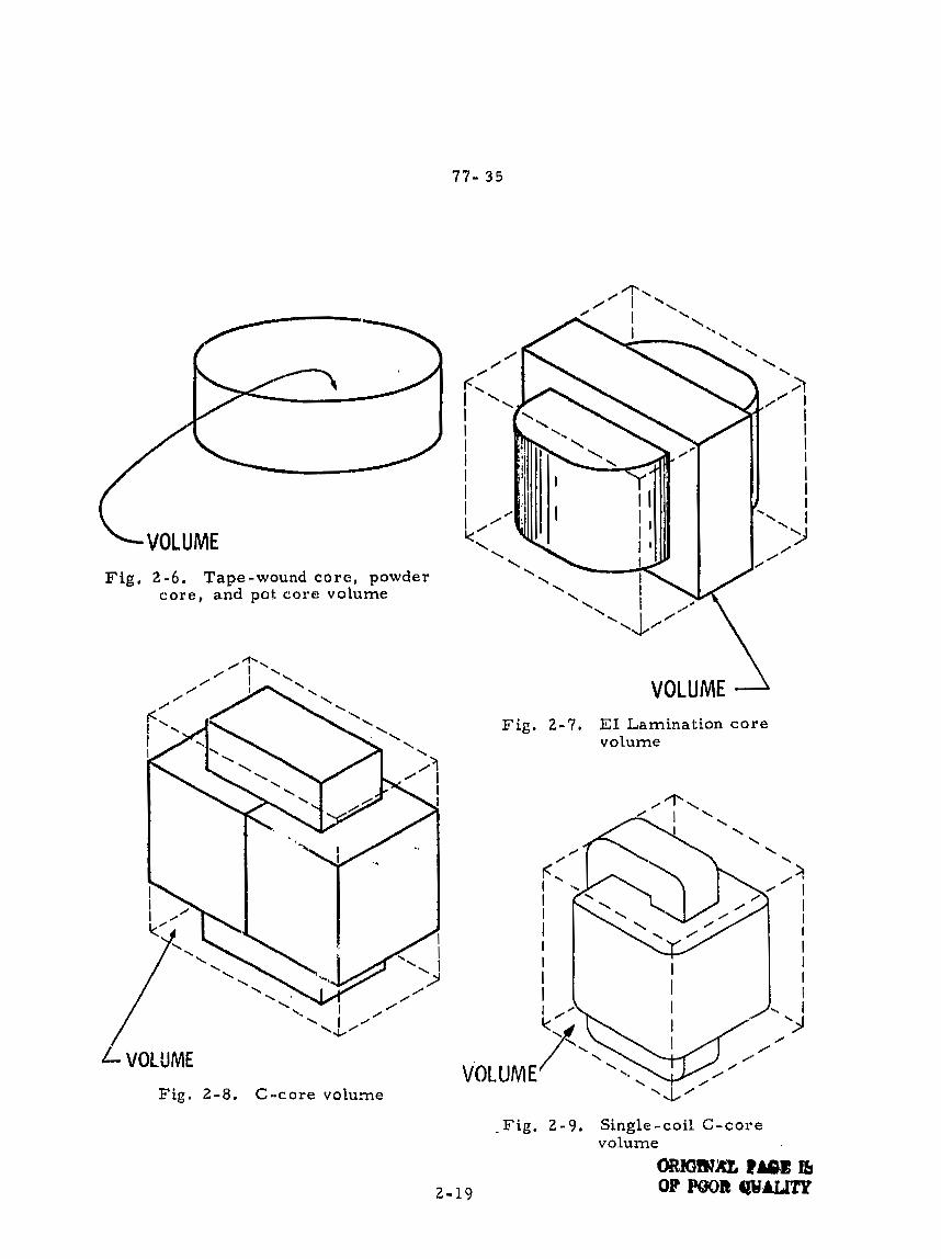
Fig, 2-6. Tape-wound core, powder core , and pat core volume
VOLUME 1 Fig . 2-7. EL Lamination core
volume
L VOLUME F i g , 2-8. C-core volume
_F ig . 2 - 9 . Single-coil C-core volume
mmmm ?*B I& PWb WUSrY

V o l = K A 0. 75 v P
The volurre,/area product relationship is
Vol = K A 0.75 V P
in which K, i b s constant related to core configuration, these values are given
in Table 2-8 . This constant was obtained by averaging the values in Tables 2 - 2
through 2 - 7 , column 15 .
The relationshi~ between volume and area product A for various core P
types is given in Figureb Z- 10 through 2- 1 5 . It was obtained from the 'ctta
shown in Tables 2 - 2 through 2 - 7 , in which the Vol and A values arc shown i n P
columns 15 for volume, and column 3 for area product.
Table 2 - 8 . Constant K,
Core type
Pot core
Powder core
Lamination
C-core
Single -coil C-core
Tape-wound core
xxr
14, 5
13.1
19. 7
17, 9 2 5 . 6
25. 0

1 -
POT CQRES
.+' 0, I 1 # + 8 m n t 1 I t 1 4 , t 8 l 1 I t t t t h l ~ I 1 1 1 , 1 1 1 1 I 1 r l , l I
. JOI 0,01 0.1 I 10 12 AREA PRODUCT, A+,, cn14
Fig . 2-10. Volume v e r s u s area product A for pot cotaes P
AREA PRODdCT, Ap, em4
r OW
Fig . 2-11. Volume versus area product A f o r powdel- cores P
, , I ' I I ' I 1 I I I , I , I -,- -
I00 - -
m 5 9 3
10
1
-
POWDER CORES
I L I l l I I I ,
0.01 0.1 1 10 100 1000

LAMINATIONS
AREA PRODUCT, A ~ , cm4
Fig. 2 - 1 2 , Volume versus area product A for lan~ina t ions P
Fig. 2 - 1 3 , Volume versus area product A for C-cores P
1000 I I I I 1 I I ( I ( I I I 1 I 1 1 1 1 I 1 I t -
loo
lo
- -
- OF PWR ALIW
1
C-CORES
1 1 I I 1 I 1 I , , I I 1 I , I L I I l -
0.01 3 I , !
0. I I t 0 IOG 1000

SINGLE-COIL C-CORES I
Fig. 2 -14 . Volume v e r s u s area product A for single-coil C-coree P
ARLA FRODUCT, A,,, em4
Fig. 2 - 1 5. Volume versus area product A f o r tape-wound to ro ids P
2-23

ZV. TRANSFORMER WEIGHT
The total weight W t of a t r a n s f o r m e r can bc related to thc area producl
A Derivation of the relationship i s according to the iollowing: weight Wt P '
va r irs in accordance with the cube of any linear dirnc~zsion O (dcsignatcd f 3 below), whereas area product A varies as thc fourth power:
P
T h e weight/area product relationship

in which Kw is a constant related to core configuration, is shown in T.rblc 2 - 9 ,
which has been derived by averaging the values in Tables 2 - 2 through 2 - 7 ,
column 14,
The relationship between weight and area product A P for various core
types is given in Figures 2-16 through 2-21 . It was obtained from the data
shown in Tables 2-2 through 2 - 7 , in which the Wt and Ap values are shown in
column 14 for weight, and column 3 for area product.
Table 2 - 9 . Constant Kw
lono - 1 1 1 1 1 1 1 1 1 I I 1 1 1 1 1 1 I 1 1 1 1 1 1 1 1 1 1 1 1 1 1 1 1 1 l l l l l r
100 - k I 5- 0 3
10 -
POT CORES
1 I 1 1 1 1 1 1 1 1 I 1 1 1 1 1 1 1 1 I I 1 1 I # I t ! I I 1 1 1 1 1 1
0,001 0.01 0.1 10 loo i AREA PRODUCT, Ap, cm
Fig. 2 - 16. Total weight versus area product A for pot cores P
2-25
I
Core type
Pot core
Powder Lamination core C-core Single-coil C-core Tape-wound core
,
1 68.2 66 .6 7 6 . 6 82.3

F i g , 2-17. Total weighl: versus area product A for powder cores P
Fig, 2 - 18. Total weight versus area p,roduct A for laminations P
2 - 26

Fig. 2-19, Total weight versus rlrca product A fo r C-cores P
Fig. 2-20, Total weight v e r s u s area product A for single-coil C -cores P
L0,000 I I I 1 - - -
I -
I- / - loo0
t i2
- -
- - - - +- r u - 5
- -
O 0 0.01 , , , , 0,1 I .o 10 I00 , , , ,,; 1000 10
-
SINGLE-COIL C-CORES
I d - 1 1
AREA PRODUCT, A,, cm4

Fig, 2-21, Total weight vereus area product A for tape-wound toroide P
E. TRANSFORMER SURFACE AREA
The surface area A of a transformer can be related to the area product t A of a transformer treating the surface area as ahown in Figures 2-22 P
through 2-25, Derivation of the relaiionships i s in actiordance with the square
of any linear dirneneion f (designated t 2 below), where area product variea as
h e fourth power:

= SURFACE AREA nod I
At . T!-VOUND + + ODWOUND XIHTCORE + ODWOUND - ~ D C O R E I
Fig. 2-22. Tape-wound core, powder cure , and pot core
surface area A t
At SURh.4CE ARfA
At LAMINATION - 2 (FE t SF + 5E - DA - 2DCl
S = BUILD
1 ~ ~ ~ O ~ ( ~ C + A I + ? ~ F E ~ S F ~ ~ E - D A - ~ D C ~ A t ' 2
Fig . 2-23 . EI larflination surface a rea A
t;
Fig . 2-24. C , - - C O ~ ~ surface area A t
F i g . 2-25. Single-coil C-core surface area At,
2 - 2 9

The surface area/area product relationship
in which K is a constant re1,ated to core configuration is shown in Tahle 2- 10, 8
wnich hae been derived by averaging the value s i n Tables 2 - 2 through 2 -7 ,
column 2 .
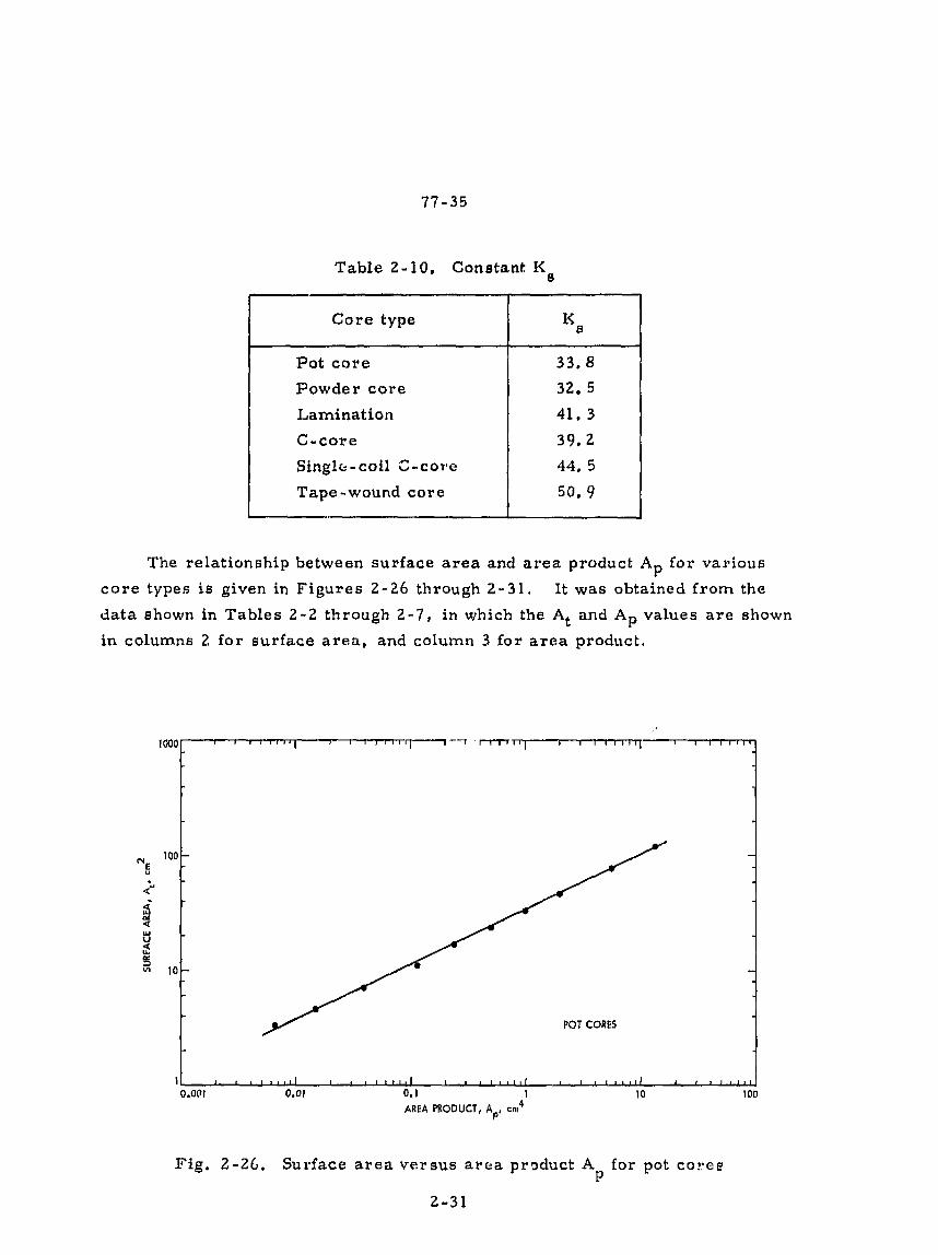
77- 35
Table 2-10. Constant KB
The relationship between surface area and area product Ap for various
core types is given in Figures 2 - 2 6 through 2 - 3 1 , It was obtained from the
data shown in Tables 2 - 2 through 2 - 7 , in which the At and Ap values are shown
in columns 2, for surface area, and column 3 for area product.
Core type
Pot core
Powder core
Lamination
C-core
Singli: -coil 2-cor"e
Tape-wound core
K a
3 3 , 8
32. 5
41, 3
39.2
44. 5
50. 9
Fig. 2-26. Surface area vcr sus area p r ~ d u c t A for pot c o r e @ P
1000 r 1 1 1 I 1 1 1 I I I I ~ I ~ / - - - I - ~ t7-rr-q I I I 1 1 1 1 1
100- I 4"
s' a! u fi 3
10-
POT CORES
i - 1 1 1 1 1 1 r I I t I I I ~ I L L a I E I I I I I I 8 t 8 0 ( 1 1 I t j J , I , L 0.001 0.01 0. I t 10 100
AREA PRODUCT, A ~ , ern4

Fig. 2-27, Surface area versus area product A for p o w d c ~ rorcs P
Fig , 2 - 2 8 . Surface area ve-~+sus area product A for laminat ions P

Fig. 2 - 2 9 , Surface area versua area product A for C-cores P
1000P
w 100- I 4-
a
&! g u 8 a " lo
5IYGI.E-COIL ' C-CORES
9 1 , -77
___-1 i
- -
C-CORES
AL CORES
F ig , 2-30. Surface area versns a r e a product A for sinsic-coil C -co re s P
1 I..,.. 0.01 0. I 1 10 100 I I 1000
AREA PRODUCl, Apr cm 4

F i g , 2-31 . Surface area versus area product A for tape-wound toroids P
too -
F. TRANSFORMER C U R R E N T DE??.'SITY
1
Current density J of a transformer can be related t o the area product A P
oi a t.ran6iormer for a given temperature rise.
TAPE WOUND TOROIDS
1 I 1 I I I 1 I I t I 1 I t
The relatianehip of current density 3 to the area product A for 2, g iven P
temperatlre rise can be derived as follows:
0,Ol 0.1 I 10 100 1000
ARE& PRODUCT, A,, rm4

d 2 . cu -. A,,, J R
Siilcc M L T has n ditucnsian of 1t?ngth
A s s u ~ . u i i i g thc cori3 l o s s i s I h c san1~7 as thc caplscr Loss for optimizrcl tr;~ns-
formrr opc ra t i un ( S c c Chstplcr 7).
P,, - p .b IDlc ( 2 - 3 9 ) 3 Cll

The current density/area product relationaI~ip:::
in which K, is a constant related to core configurat ion, i s shown i n Table 2 - 11, J
which has been derived by averaging the values i l l Tables 2 - 2 through 2 -7,
colurr~ns 9 and 1 3 .
::<This is the theo1:rtical value for cu r ren t densi ty/ar ea prodrlc t r ela.tions11ip. The empirical values for different core colzfiguration are found in Table 2-1,
2 - 3 6

77- 35
Table 2 - 1 1. Constant K j
Core type K.(A2Ei0) K (A.50") 1 j
Pot core
Powder core
Lamina tion
C-type core
Single-coil C-core
Tape-wound core
The relationship between current densi ty and area product A for a tempera- P ture r i s e of 2 5 ° C and 50°C; is given in Figures 2 - 3 2 through 2-37. I t was obtained
from the data shown in Tables 2 - 2 through 2 - 7 , in which the 5 and A values are P
shown in columns 9 and 1 3 for curl ent density, and column 3 for area product.
I I--'
1000 - P, = OUTPUT POWER
PC,, COPPER LOSS = Pie IRON LOSS N
PC, Py: - PC,, + "fc -7 - P"
C
u
200 -
Lll 0.01 0.1 1 ~ l ~ l I 1 10 a 1 , I l 100 I 1000
POT CORES
la0
AREA PRODUCT, Ap, crn 4
Fig . 2 - 3 2 , C u r r e n t densi ty versus area product A for a 25°C and 50°C rise for pot cores P

POWDER CORES
Fig, 2-33. Current density versus area product F. for a 25°C and 50°C rise for powder cores P
r 19 OJ.ITPUI rc;weE Boo
1 0 0 0 ~
PC, CC3YPLI LOSS - IRON LOSS
cl&.l 1 8 1
LAMINATIONS
100 0.01 0.1 1 10 100 10119
AREA PRODUCT, A ~ , cm4
Fig, 2 - 34, Cur ren t density versns area product A f o r 2 5 c C and 50°C rise for laminations P

PRLA PRODUCT, Apt crn 4
Fig. 2 - 3 5 , Curren t density versus area product Ap for 25°C and 50°C r i s e for C-cores
C RISE
C RISE
SINGLE-COIL <-CORES 1
F i g , 2 - 3 6 . Cur ren t density versus a r e a product A for a 25°C arid 50°C r ise for single-coil C-co res

Po OUTPUT POWER 4 800 - PC,, COPPER LOSS PIL' IRON LOSS - -
P" PI: PC,, + PIC 1~ - "U
- - -
-
200 -
100 I 1 I I I I , , I
0.01 0. I 10 100 1000 AREA PRODUCT. Apt c f
Fig. 2 -37 . Cur ren t density versus area product Ap for 25°C and 50°C r ise f o r tape-wound toroids

CHAPTER 111
POWER T R A N S F O R M E R DESIGN

A . INTRODUCTION
The conversion process i n power e l e c t r o n i c s requires the use of
t r a n s f o r m e r s , components which f requent ly are the h e a v i e s t and bulkiest i t e m
i n the conversion c i rcu i t s . They a l s o have a signif icant effcct upon the o v e r a l l
performance and efficiency of the s y s t e m , Accordingly , the des ign of such
t r a n s f o r m e r s h a s an i m p o r t a n t influence on overa l l s y s t e n l weight, power
convers ion eff iciency and cos t . Because of the i t r terdependence and interactioa*.
of parameters, judicious t r a d e o f f s are n e c e s s a r y to a c h i e v e design optimizat ion.
THE DESIGN PROBLEM GENERALLY
The d e s i g n e r is faced with a set of c o n s t r a i n t s which must be observed
in the des ign of any t r a n s f o r m e r . One of t h e s e is the output power , Po,
(operating vol tage muitiplied by m a x i m u m c u r r e n t d e m a n d ) which the secondary
winding m u s t be capable of de l ive r ing to thc l oad withilt s ~ e c i f i e d regula t ion
limits. Another r e l a t e s t~ m i n i m u m efficiency of opera t ion which i s dependent
u p o n the maximum power l o s s which can be al lowed in Ih2 t r a n s f o r m e r . St i l l
a n o t h e r def ines the maximum p e r r n i ~ l s i b l e tempel*atur+ rise for the t r a n s -
f o r m e r when u s e d in a spec i f i ed t e m p e r a t u r e envi ronment .
Other c o n s t r a i n t s relate to volume occupied by t h e t r a n s f o r n e r a n d
p a r t i c u l a r l y i n a e r o s p a c e appl ica t ions , weight , s ince weight min imiza t ion i s
a n impor tant g o a l in the d e s i g n of space flight e l ec t ron ics . Las t ly , cos t
e f fec t iveness is always a n i m p o r t a n t cons idera t ion .
Depending upon applicat ion, c e r t a i n of these c o n s t r a i n t s will dominate .
Parameters affect ing o t h e r s m a y then be t r a d e d off a s n e c e s s a r y t o achieve
the most d e s i r a b l e design. It is not poss ib le t o opt imize a l l parameters in a
single design b e c a u s e of the in te rac t ion and inte;dependenc,n of p a r a l n e t e r s .
For example, if voluine and weight a r e of g r e a t s igni f icance , r educ t ions i n
b o t h often can be effected by operating the t r a n s f o r m e r at a higher f r e q u e n c y
but a t a penalty i n efficiency. When the frequc,l ,- cannot be r a i s e d , reductic.n
i n weight and volume m a y s t i l l be poss ib le by se lec t ing a m o r e efficient core
Preceding page blank

material, but at a penalty of increased cost , Judicious tradeoffs thus must be
ef fected to achieve the design goa l s .
A flow chart showing the interrelation and interaction of the varioua
design factors which murrt be taken inta consideration i s shown in Figure 3 - 1 .
.. "
L AP f flux density
w area-product frequency -9 I 1
1 r J current density n4- - 4 - 9 I
t CORE CONFIGURATION KNOWN
I I
CORE LOSS - mllliwatts/gram 7
4 t ' I
1 r ,, TRANSFORMER COPPER LOSS I I I
WEIGHT
I -
CORE - - MATERIAL
4 t 1 T
I 1 REGULATION
YlGH FREQ I I
A SKIN EFFECT I t - I 4 I
TRAN SFORMER FLOW CHARI '
Fig. 3 - 1 . Transformer design factors flow chart
Various transformer des igners havt: used different approaches in arriving
at suitable designs. For example, in many c a s e s a rulr? of thumb i s used far
dealing with current density. Typically, an assumption is made that a good
working level is 1000 circular mils per ampere. This wi l l work in many
instances but the w i r e size needed to meet this requirement m a y produce
a heavier and bulkier transformer than desired or required, The information
presented herein makes it possible to avoid the u s e of t'his and other rules of
thumb and to develop a more economical deaign with great accurac;y,

C, RLLATIONSI-IIP OIq' A TO TRANSFORMER POWICII HAND LINE CAPABILITY
Accol-ding to the newly dovclopcd approach, thc powcr handling capabil i ty
of a core is rclatcd to its area product by a n equation which may brl s t a t cd as:
K = w a v c f a r m coefficicnl
4.0 square wave
4 , 4 3 s ine wave
= flux densi ty, t e s l a
f = frequency, EIz
K I; window uli l izat ion factor (scr: C l ~ a p t c r 6 ) U
I< - c u r r e n t dcnsi ty cocfficicnt ( s c c Chapte r 2 ) j
Pt = apparcn t power , primary plus secondary
From the abovc it can bc s c c n that factors such a s flux densi ty, frccluctlcy
of opera t ion , u ' i n d o v ~ ut i l iza t ion fac to r K ~ , ~ ~ i c h d e f i i ~ e s the maximum spacc U'
which may be occupied by the copper i n the window, ancl the constant K which j '
is rclatcd to t cmpcra ture r i s c , all have an influence 011 the t r a n s l o r ~ l ~ c l . a r c a
product . The constant K. i s a ncw paramctcr that g i v c o the dcsigncl. cont ro l J
of the copper loss. r)~tS:.~rLtnn is sct f o r t h i n dc ta i l in C h a p t e r 2. The dcr ivat ion
for area p r o d u c t A p is set fortl . : i n dctail a t the end of this c h a p t c r AppcncI ix 3 . A .
D, OUTPUT P O W E R VS I N P U T P O W E R V S A P P A I I E N T P O W E R CAPABILITY
Output power (P ) is of g r e a t e s t i n t e r e s t to thc u s c r . T o the t r a n s f o r ~ n e r 0
d e s i g n e r it is thc apparent p o w e r {Pt) which i s assoc ia ted wi th t h c g e o m c t r y d
the transformer that; is of g rea t e r i n ~ p o r t a n c c . A s s u m c , for the salcc of
s impl ic i ty , the core of an i so lz t ion t l - a n s f o r m c r has but two \v inc l ings i n t l ~ c
wit~clow a r e a (W 1, a p r imary a n d a sccondary . A l s o assulnc that the window a
3 - 5

area (W,) is divided up in p r ~ . . o r t i o n to the powcr handling capability of thc
windinge using cqual cul*rcnt d ~ n s i t y . Thc pr imary winding handlcs Pin and
thc accondary h a n d l c s Po to the laacl. Slncc thc potvcl- t r a n s f o r m c r h a s to bc
Jesigncd to a c c o m m o d a l c thca primaiWy P a n d secondary Po, then: in
Tlzc d c s i g n c r m u s t bc concci*ned with thc appaltcnt powcr handl ing
capabil i ty, Pt, of the t r a n s f o r m e l co1.c and w ind ings . Pt may va ry by a
factor ranging f r o m 2 to 2 , bL8 t imes the input p o w e r , Pin, depending upon
the type of circuik in wl~ic l l the t r a n s f o r m c r i s u s e d . II the cu r r cn t in t hc
tectificr t r a n s f o r m e r bccorl~cs interi*uptcrl, its cflect ivc R M S va luc changcs,
Trans fo rmer s i t e , thus, is not only dctcrmined by the load d c ~ l ~ a n c l bul, also,
by application bccausc of 111c cliifcrcnl c o p p e r lossrs l~ lcurrec l d u e to currcn t
waveform ( s c c Chapter 7, F i g . 7-20) .
F o r example, f o r a load of one wat t , compare the powcl- handling capabil-
i t ies requ i red for each w i n d i n g (neglect ing t r a n s f o r m c r and diode 1o:scs so tha t
Pin = P ) for the fu l l -wave b r idge circuit: of Fig. 3 -2 , the fu l l -wavr center . - 0
tapped secondary c i rcui t of F i g . 3 - 3 , a n d the p u s h - p u l l ccntc:.-tapped fu l l -wave
c i r c u i t in Fig. 3-4 , w h e r e a l l winclings havc the same number of t u r n s (N).

SQUARE WAVE
I 2 Fig. 3 - 2 , Full-wavc bridge circuit
The total apparent p o a v r Pt for the circuit shown in Fig. 3-2 is 2 watts. This
is allown in the following equation:
in which and IN2 are the currents associa.ted with the primary and
secondary windings, respectively, and E and ENZ are the voltages acrass N1 the primary and secondary windings, respectively.
Fig . 3 - 3. Full-wave, center -tapped cilqcuit
3 - 7

The total power Pt for t:;e circuit ehown in Fig, 3 - 3 increased 20. '1%
due to the di~ltorted wave form of the interrupted current flowing in the
secondary winding, Thia i a shown in the following equation:
Rewriting equation 3 - 5 to Incorporate the RMS rating,
LOAD l W
Fig. 3- 4. Push-pull, full-wave, center -tapped circuit
The total power Pt for the circuit ehown in Figure 3-4, which is typical of a dc
to dc converter, increases to 2 .828 times P. because of the interrupted cur- in rent flowing in both the primary and secondary windings since

Again,
Thus the circuit: configuration in which the transformer ie to be used
must be considered by the designer when sizing the transformer.
Rather than diecues the various methods ueed by transformer designers,
the author bel ieves it will be mcre useful to consider typical design probl.ems
and to work out eoldtions using the approach baaed upon the newly formulated relationships.
E. A 2.5-kHz TRANSFORMER DESIGN PROBL. ' ~ 5 ; AN EXAMPLE
Assume s specification for a transformer design as shown in Fig, 3-2,
requiring the following:
(1 1 Eo' 10 volts
( 2 ) Iol 2 . 0 amperes
( 3 ) Ein, 50 volts
(4) f , 2500 Hz (square wave) ~~~~ PaE Ib
(5 ) M a x i m u ~ i temperature r ise , 25" C OF P W R Q U U ~
(6 ) Transformer efficiency, 95%
Assuming the bridge rectifier of Fig, 3 - 2 and using the efficiency
const -.. ink of 9570:

Deiinitians for Table 3-1
Information given is listed by column as:
Manufacturer part number
Surface area calculated from Chapter 2, Fig. 2-24
Area product effective iron area times window area
Mean length turn on one bobbin
Tota l number of turns and wire size for two bobbins using a window utilization factor K = 0.40 U
Resistance of the wire at 50" C
W a t t s loss is based on Fig. 7-2 f o r a AT of 25°C with a room ambient of 25°C surface
dissipation times the transformer surface area, total loss is equal t o 2 PcU
Current ca-lculated from column 6 and 7
Current density calculated from column 5 and 8
Resistance of the wire at 75'C
Watts loss is based on Fig, 7-2 for a AT of 50°C with a room ambient of 25" C surface
dissipation times the transformer surface area, totzl loss is equal to 2 PcU
Current calculated from column 10 and 11
Current density calcdated from column 5 and 12
Effective core weight in grams
Copper weight in grams
Transformer volume calculated from Chapter 2, Fig, 2-8
Core effective cross- section

Table 3-1, C-core characteristics
1
2
3
4
5
1
'vDTC
A L - b
AL-3
AL-5
AL-i,
AL-124
a 3 4 5 6 7 8 9 1 O 11 12 13 l a ' Is I 16 1 17
af ZS-c
20.9
23.9
35.6
37.;
45.3
7 AL-9 69.0 3.09
D.265
O.;lO
0.767
1.OII
1.4;
i . 3 8
9
10
11
12
I3
1
15
I6
63.4 2-33
4-58
j.59
3
5 50
221 20
AL-12
AL-135
AL-78
AL-la
A L I 5
AL-16
AL- i7
XL-19
i. 7-1
copper 2m.a = fmn loss
17
18
19
20
661 30
b6230
q 4 6 3 ~
9*30
jg
P . = 3 i
7.81
7 .
7.3b
7-01
7-61
5-56
1 ~ 0 i
0
7.33
87.0
93.7
48.1
118
I Z P
127
142
1%
f" 20
6 3:
b37 zO
e. iR 2 0
221 20
O + i a w
O.:-tR
0.908
O.RU
1-47
21 1
- 201
LOO
178
tZ1 20
2:s 20
3Zi -0 . 31b 20
510 La
1-Iff,
1.0i1
1.034
0- 92.2
AL-LO
AL-22
AL-23
AL-24
4.57
5-14
6. D7
r. 92
9.07
LO. B
14.4
IB.0
2.23
L.7B
3.07
4-32
ern
8 . 9 3 D . t Z i 0 la7 Q. El 1 . 4 a 2 1 3 1 538
10 ; 0 . 1 9.18; I t 3 O.2,? 53 1
16.5 1.01 0.174 14% 18.1 2 3 0.255 503
L-OT 4
1b.x
27.5
0. iiC
2 . 5
3 0
8.05
B. e9
10.3
10. ir
182
LO5
220
245
Zi. k
2.24
2 61
2.61
2.94
3 . 5
1,VC
L&(.
2%
2%
zi 1
1 7
8 i . l
1 -38
I . 32
1.24
1 . 3 3
I 10
3 . 5 6
3.80
4-25
.
3R6
186 20
jBb LO
311 ZO
LL. b l1.B
I . 1L
1.1) D.ITL
23:
233
2%
20;
0- id-
I 3 . 3 l S . i
4.7: / 17.1
1.23
1.20
l .IR5
1.Ot.i
1.18
1-30
1.3
L.10
28.0
34.9
4P. D
l . i D 1
0.t14r
0-bLI
0.9UT
J.91.Z
1.61
1. bl
1. SL 11.3
11.1
12.0
C. liS
311
1.30
1 . 4 3
I -t.+.
2.31
4
310 437
293 489
1-51
t.35
271
2.03
5.22
6
t.5~
7
u
291 612 3BZ 24L67 4.48 f
259 552 538 L80.91 3.58 L
3 I O
' 0 . 1
3 . ~ 0
B.NQ
0 .
11.1
0.529
45: 41. i 23.40 It,tl8 h 7 1 1 f
2 01
1-43
1.81
1-95
1-60
3C.Z
307
345 113 1 9-63 1.26
374 I55
303
1-79
1-76
1-73
l .55
4-44
346
WD 235
333
299 328 I
2.05
3.1: o.rl.9

100
f ro L cn 10 4 V) C C
B - - - .- €
& m 0 2 L.J = 1.0 8
s%, .g"e a s
0.1 2.5 KHz e6.0 KHz ,Z10,0 KHz 1.10.0 KHz m 2 5 KHz
2 mil MATERlAL 2 mil MATERIAL 2 nil MATERIAL 1 mil MATERIAL 1 mil MATERIAL
MA#ETI C MAlER l AL COMPAR I SON F.T A CONSTANT FREQUENCY
St3 Fig. 3- 5. Magnetic material comparison at a constant frequency

Step No. 1. Calculate the apparent power Pt from equation 3 - 5 , -- allowing for 1 .0 volt diode drop (Vd) a~sumed:
Step No. 2 . Calculate the area product A from equation 3- 1 : P
Assuming
I3 = 0 . 3 m
KU = 0 . 4 (Chapter 6 )
K . = 323 (Chapter 2 ) J
[watt.]
[ te sla]
After khe A has been determined, the geometry of the transformer can be P
evaluated as described i n Chapter 2 for weight, fo r surface area, and for
volume, and appropriate changes made, i f required. Having established the

configuration, it is then ncccseary to determine the core rnatc~*ial to co~nplctc
core sclection.
Stcp No. 3 . 3clcct a C-core from Table 3 - 1 with a valuc of A closcsl; t o i3
the one calculated.
Stcp No. 4. Calculate the total transformer losses Px:
[watts]
Maximum efficiency i s realized when thc copper (winding) losses arc
equal to the iron (core) losses (see Chapter 7):
and therefore
and thus

Stcp No. 5 , S ~ l c c t the core weight fl-nn~ Tablc 3- 1, column 14, then
calculate thc ca rp lass in nlilliwatts per giqnnl:
Stcp No, 6 . Scluct t l ~ c pr*oprlo n~agnct ic inatcrial i n F ig . 3 - 5 , rr-adin::
f rom thc 2 , 5 Icllz frequt qcy curve lol* a flux density of 0. 3 t~ns l r~ . Tlicl m,rgnr+t ic
m a t e r i a l that: comes closcsl t o 1 3 , 5 n ~ i l l i w a t t s p c r gram is s i l i c o n ~ t ~ r . 1 , \\+ilh
appl.oximatcLy 12 m i l l i w a t t s pcr g l - a m . With a weight of 46.6 g14alns, the" total
cot*o loss is 5 6 0 n ~ i l l i w a t t s , wl~ich nwcts the ~ ~ c q u i r c r n ~ n t : of thu ~*lr\sigt!,
Stcp No. 7 . Calculate the nunrbci* of p r i m a r y tut-ns using E ar*arlay1s lr.\r., >;c
equation 3 , A- 1,
The itqon cr-oss section A is found i n Table 3 - 1 , column 17: (J
*: See Appendix 3. A, at the e tld of Cllaptc 1. 3 .

N = 2 3 3 turns (primavy) P
Stcp No. 8. Calculate the currcrit density J from rruation 3 , A - 17:
(The value for K, is found in Table 2 - 1 , ) J
Step No. 9. Calculate the primary cu r r en t I and w i r e size Aw: P
The bare wire size A w(B)
for the primary is

Step No. 10, Select the wire area Aw in Table 6 - 1 fur equivalent (AWG)
wire eize, column A,
AWG No. 25 = 0 .001623 LCrn21 The rule ie that when the calculated wire aize does not fall close to those l isted in the table, the next smaller aize ehould be selected.
Step No. 1 1 , Calculate the resistiince of the primary winding, using
Table 6-1, column C, and Table 3 - 1 , column 4, for the MLT:
Step No. 12. Calculate the primary copper lass PcU:
P = 1 2 ~ cu P P
Step No, 1 3 . Calculate the secondary turns: -
[watt El]

Step No. 14. Calculate the wire a izc A w(B for the secondary winding:
Step No. 15. Select the wire area Aw in Table 6 - I for equivalent (AWG)
wire rrize, column A:
AWG No, 19 = 0.006 53 LC,2] The rule i o that when the calculated wire size doee not fall c l o s e to those
listed in the table, the next smaller size should be selected.
Step No. 16. CalcuIate the res i s tance of the secondary winding, using
Table 6-1, column C , and Table 3 -1, column 4, for the MLT.
R a = MLT X N X (column C ) X 6 X Ln 1
Step No. 17. Calculate the secondary copper loss PcU:
[watt .I

Stop No, 18. Sunlmariac the lorrsc?e and compare with thc total
losses P : 2;
Primary
Total P, = 1 . 2 7 9
Thc total pawcr l o s s in the L r a n ~ f o r n ~ u r is 1 , 279 watts , which w i l l cffcclivcly
nlcct thc rcquircd 95Ofo efficicncy,
Froin Chapter 7, t l~c surface arc:? .P rcquirccl to dissipate waste hrlat t !exprcsacd as watts l o s s per unit a r c a ) I,
Reforring to Table 3 - 1 , column 1 , for the AL-124 sizc core, the surfaca arca
A~ i~ 45.3 cm2:
and thus

11 = o. 02112
which will produce the required temperature rise,
Fa A 10-kESz TRANSFORMER DESTC;?! PnOBL EM AS AN @XAMPLE
Assume a epecification for a transiormcr des ign, as shown i n Fig, 3 - 3 ,
requiring the following:
(1) Eo, 56 volts
(2) ya, 1.79 amperes
( 3 ) Ein, 200 volts
( 4 ) f , 10 kHz (squar~ wave)
( 5 ) Maximum temperature rise, 25" C
( 6 ) Traneformer eff iciency, 98%
assuming the full-wave, center-taped rectifier of Fig. 3 - 3 and using thc
efficiency constraint of 98%.
Step No. 1. Calculate the apparent power Pt f rom equation 3 - 10, allowing
for 1 . 0 volt diode drop (Vd) a~~urned:

Stop No. 2. Calculate tllc aroa product A from equation 3 - 1 : " P
assuming
I< - 323 (Chapter 2 ) j
after t l ~ e A Ins been d e t c r ~ n i n e d , the geometry of thc transformcr can bc P
evaluated as descr ibed it1 Chapter 2 for weight, for surfacz area, and for
volume, and appropriate changes made, if required, Having e s tablishecl the
configuration. it i s t h e n necessary ta determine the care material to cornplctc
core s c l c c t i ~ n .
Step No. 3 . Select a C-core t rnrn Table 3 - 1 with a valuc of A oloscsl: I'
to thc one calculated:

Stcp No. 4 . Calculata thc total transformer losses P : z
watts I
Maximum efficiency is realized when the copper (winding) loasca arc
cclual to the iron (coye) losses ( m e Chapter 7) which i s cxprcssed as
and thurefora
and thus
Stcp No. 5. Select the core weight from Table 3-1, Column 14 , thcn
calculate the core loss in milliwatts per gram:
AL-8 Wt - 66.6 grams

Stcp No. 6 , Sclect the proper magn'tic material in F i g , 3 - 5 , rt:adinp
from the 10-kHz ircquc~~cy curvt? wit11 a density of 0. 3 1:csla. Thc magnut i c
m a t e r i a l that c c m c a closest t~ 15.6 mill iwatts per g r a m is P o r l n a l l o y RO, w i t h
approximately 12 m i l l i w a t t s pclg grain. Wllcn r~iclccl stocl i s usccl, Tat lo 7 - 1
p r o v i d e s a weight col.rc.ction factor.
Tllc wcight f r o m Tablc 3 - 1 i s multiplied by the we igh t c o r r o c t i o n factov:
With a weight of 7 6 , 2 g ran .8 tile total co l - c loss i s
Step No. 7 . Calculatc tllc r~un~bcr of primary turns using F a r a d a y ' s law,
e q u a t i o n 3. A- 1 :
Tllc i r o n c r o s s s e c t i o n Ac is found in Table 3- 1 , co lumn 17:
N = 207 turns (primary) P

Stcp No. 8, Calculate the current dens i ty J from equation 3 , A- 17:
J = IC,A -0.14 J
The value for I<, i s fo~ rnd in Table 2 - 1 : J
J - (323)(2, 31 ) - 0 , 1 4
J = 287
Step No. 9. Calculate the primary cu r ren t I and w i r e size Aw: - P
Tlic barc wire s ize l o r the primary is
Stcp No. 10. Sclect the w i r e area A w(B
i n Table 6 - 1 far equivalent
( A W G ) wire s ize, column A:
AWG No. 2 5 = 0.001623
The rule is that when the calculated w i r e s ize docs not fall close t o those l is ted
i n the table, the next smaller size should be selected.

Stcp No. 11, Calculate the resistance of tnc primary winding, using
Tablc 6 - 1, column C , and Table 3 - 1, column 4, for tho MLT:
R = MLT x N x (column C ) x 5 x l o e b P
In I
R - (5.74)(207)(1062)(1.098) X l 0 - b P
R ;: 1 . 3 8 P
Step No. 12. Calculate the primary copper lose PcU:
2 P = I n =u P P
2 P (0,520) ( 1 . 3 8 ) CU
Step No, 13. Calculate the secondary turns:
[n 1
1, watts 1
[ watts j
N = 5 9 turns secondary 9

Step No. 14. Calculate the wire size A w m 1 for the secondary winding
( s e e equation 3-8):
Step No. 1 5 . Select the bare wire area A w(B 1 in Table 6 - 1 for equivalent
(AWG) wire size, column A:
AWG No. 21 = 0.0041 1
The rule is that when the calculated wire size does not fall close to thoae listed
in the table, the next smaller size should be selected.
Step No. 16. Calculate the resistance of the secondary winding, using Table 6-1 , column C, and Table 3-1, column 4, for the MLT:
Step No. 17. Calculate the total eecondary copper 108s P NZ p l u ~ N j CU'
(see F i g . 3 - 3 ) :
P = (IO X 0.707)' R i (Io X 0 . 7 0 7 ) ~ RB [ watts 1 CU 5

FCU = 0.499 [ watts I
Stcp No, 18. Summarize the l o s e c ~ and cornparc with the total losscs P,,: U
Primary Pcu = 0.373 1 watts 1
Corc Pfc 1,07
Total P, = 1.942
[wat ts 1
wat ts $
T h e total power loss i n the transformc r is 1. 942 watts, wl-lich will meet tllc
rcquircd 98'v0 cfficicncy.
From Chapter 7, the surface area A requircd t o dissipate wastc heat t
( cxpresscd as watts loss per unit: area) is
2 JJ = 0.03 ~ / c m at 25°C rise
Referring to Table 3 - 1 , column 1 , for thc AL-8 s i z e corc, tho surface arca A 2 t
is 6 3 . 4 c m :

4 = 0,0306
which wil l produca tho required temperature riae.
REFERENCES
1. McLyman, C,, Design Parameters of Toroidal and Bobbin Magne t i ce , Technical Memorandum 3 3 - 6 51, pages 12- 1 5, Jet Propulsion Laboratory, Pa sadc na, Calif,
2. Blumc, L, F., Transformer Engineering, John Wiley & Sons Inc., New York, N.Y. 1938. Pagcs 272-282.
3 . T e 1-marl, F, E. , Radio Enginee1.e Handbook, McGraw-Hill Book Go, , I n c . , New Yorlc 1943. Pages 28-37 .

APPENDIX 3. A
TRANSFORMER POWER HANDLING CAPABILITY
Tbc power handling ~ a p a b i l i t ~ y of a trarlsformcr can bc related to -Ap iL
quantity (w\hich. i a the W,A, product where Wa is the available core ,. window area in cmL and Ac is the ef fect ive c r a s s - ~ c c t i o n a l area of the core i n
2 cm ), as fo l lows,
A form of the E'nraday law of clectrornagnetic illduction much uscd by
transformer d e s i g n c ~ a etatcs:
(Thc constant K is talcen at 4 for squai.c wave and at 4 . 4 4 for ~ i n c w t , t \ c*
operation. )
It i s convenient to restate th is cxprcssion as:
for the following manipulation.
By definition the window utilization fact014 is:
and this may be restated as:
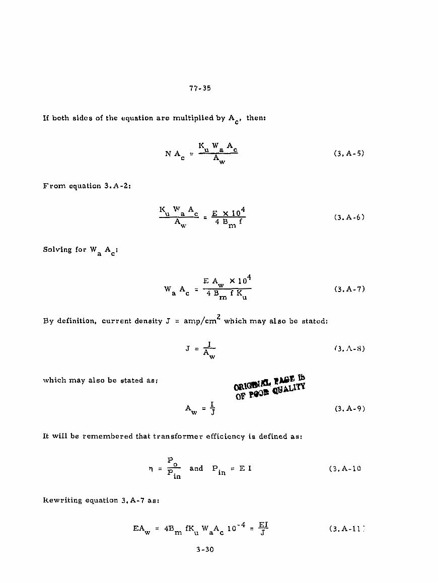
If both sidca of the equation are multiplied by A=, then:
From equation 3.A-2:
Solving for Wa Ac;
2 B y definition, current density J = amp/cm which m a y also be stated:
which may also be stated as:
It will be remembered that transformer efficiency is defined a s :
Po q = - and Pin = E I 'in
Rewriting equation 3. A-7 a s :

and eince:
then:
total Prirrlary Secondary
P x l o4 P x l o 4 x l o4 W,Ac
- - 0 0- qJ 4BmfKU + 4BmiKUJ - 4Bm€KUJ ( I / ~ + 1) t3.A-13) total
$
and since
then
Combining the equation from Table 2 - 1,

yielding

CHAPTER IV
SIMPLIFIED CUT GORE ZNDUC TOR DESIGN

A, INTRODUCTION
Design= rs have used various approaches in a r r i v ing at su i t ab le
inductor designs, For example, in many casce a rule of thumb
used for dealing with cur rent dens i ty i~ that a good working level i s
1000 c i rcu lar mils per ampere, This i s sat isfactory in many
instances; howevcr, t he wire size used to m e e t th is roquircment
may produce a heavier and bulkier inductor than desired o r required.
The information p r e s e n t e d herein will make it possible to avoid. the
use of th is and other rule6 of thumb and to develop a more econom-
ical and n better design,
B, CORE MATERIAL
Desrgners have routinely tended t o specify moly permalloy
powder c o r e mater ials f a r filter inductors used in high frequency
power convertors and pulse-width modulated (P WM) switched
regulators because of the availability of manufacturers' l i terature
containing tables, graphs and examples which simplify the design
task. Use of these cores m a y not result in an inductor des ign
optimized for size and weight , Fo r example as shown in Figure 4- 1 ,
moly permal loy powder co res operating with a dc bias of 0, 3 tesla
have only about 8070 of original inductance with very rapid lalloff
at higher clensities. In contrast , the s tee l core has approximately
four timea the useful flux density capability whi le retaining 90% of
the original inductance a t 1,2 tes la ,
There a r e significant advantages to be gained by the u se of
C cores and cut toroids fabricated from grain- oriented silicon s teel ,
dospite such disadvantages as the need for banding and gapping
matcr ials , banding tools, mounting brackets and winding mandrels.
.I. II.
See Reference 1.

POLAR1 ZED FLUX DENSITY, TESLA
Fig. 4- 1. Inductance vs dc bia a for r,ioly permalloy cores,
Grain-oriented silicon steels provide greater flexibility in the design of high frequency inductors because the air gap can be
adjusted to any desired length and because the relative perme-
ability is high even at high d; rlux denei';y. Such steels can
develop flux deneities of 1 .6 teala, with useful linearity to 1 , 2 tesla. * Moly permalloy cores carrying dc current on the other hand
have useful flux density capabilities to only about 0 . 3 tes la .
C. RELATIONSHIP OF A TO INDUCTOR ENERGY HANDLING CAPABILITY P
According to the newly developed approach the energy handling
capability of a core is related to its area product A by a equation P
which may be stated as follows: 4 - 3

K = currcnt clensity coefficient j (Sce Chapter 2. )
K a window utilization f ac to r (Scc Chapter 6. )
Bm = flux densi ty , tesla
Eng = enc?rgy, watt seconds
From the above i t can be s een that f a c to r s such a s flux density, wirldow utiliza-
tion factor KL, (which defines the maximum bpace which may be occupied by the
copper in the window) and the constallt K. (which is re la ted to temperature r i se ) , 3
al l have a n itlfluence on the inductor area product, The c o t ~ s t a n t K. is a new J
parameter that gives the designer cont ro l of the copper loss , Derivation is scl: for th in detail iu Chapter 2 ,
D. FUNDAMENTAL CONSIDERATIONS
The design of a linear r e a c t o r depends upon four re la ted factors ,
1. Dcsired inductance
2 . Direc t current
3. Alternating c u r r e n t A1
4. Power l o sa and t empe ra tu r e r i s e
With these requirements es tabl ished, the de s igne r m u s t de t e rmine the
maximum values for Bdc and f o r Bac which wil l not produce magnetic sa tura t ion,
and must make t radeoffs which wil l yield the highest inductance fo r a given
volume. Tke co re ma t e r i a l which i~ chosen dictates the maximum flux density
which can be to lera ted for a given design. Magnetic sa tura t ion values for
dif ferent core m a t e r i a l s are shown in Table 4 -1 as fo l lows.
d. .,I
Deviation is set forth in deta i l in Appendix 4. A at the end of this chapter.
4,- 4

Table 4- 1. Magnetic material
Magnee il 3??0 Si, 9770 Fe Or thonol 50% Ni, 50% Ft! 48 Alloy 4870 NNi, 50% Fe
Permalloy 7970 Ni, 17% Fe, 470 M o
Material Type
It should be remembered that maximum flux density depends upon Bdc + Bat in manner shown in Figure 4-2.
(tenla)
'.ir
Fig . 4-2 . Flux density versus ldc 4- A1
0.41rNI x10-* - d c Bdc - -
1 [t e s la] (4-2)

Combining Kqs, (4-2) and (4-3) ,
0. 4nNIdc k lom4 0 . 4 r N A1 X 10 - 4 B - -
rnax 1 1 [tcsla] ( 4 - 4 ) t rn m
's +'T;T 1 t- g Pr
Thc i~lductancc of an iron-core inductor carrying dc and having an a ir gap
m a y be expresded as:
Inductance is dcpcndcnt on thc effective length of the magnetic path which
is the sum of the a i r gap length ( 1 ) and the ratio of the core mean length to
relative permeability ( 1 m/pr) .
When the core air gap [ I ) i s large compared to relative permeabil ity g
(I , / pr), because of thc high relative permeability (pr) variations in p, do nct
substantially effect the total effective rnagne tic path lcngth or the inductance.
The inductance equation the11 reduces to:
[henry] (4-6)
Final dcter~nination of the air gap size requires consideration of the
effect of fringing flux which is a function of gap dimension, the shape of the
pole faces, and the shape, size and Location of the winding. I t s not offecl: i s to
shorten the air gap,
Fringing f l u x decr e a s ~ s tho total reluctance of the magnetic path and
therefore increases the inductance by a factor F to a value greater than that

calculated from cqunlion 4-6. Fringing fluxV i s a larger percentage o f the total
for larger gaps. The fringing flux factor is:
w l ~ c r c G is a din~ensio i~ clcfii~ed in Chapter 2 . (This equation i s also valid for
Lanlitlatiolls, )
Equation (4-7) is plottcd in F igure 4-3 bclow.
Fig. 4-3 , Ii~crease of reactor illductancc with flux f r ing ing at the gap.
Inductance L computed in equation (4-6) does not include the effect of
f r i ng ing flux. The value of inductance L' correctltd for fr inging flux is:
41- 1,.
See Reference 2 .
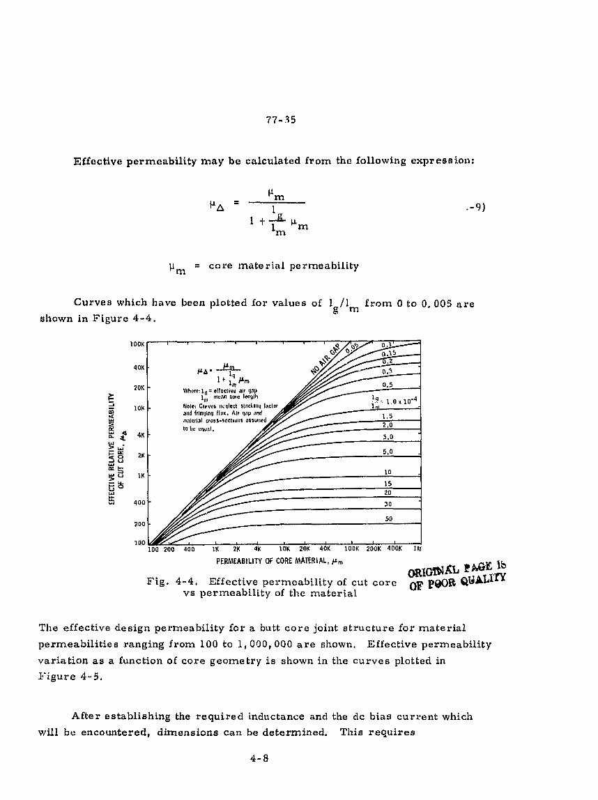
Effcctlvo permeability may be calculated from the following exprasaio~~:
nl = core material permeability
Curves which have been plotted for values of 1 / I f rom 0 to 0. 005 a re 6 m
shown in Figure 4-4 .
PERMEABILITY OF CORE MATERIAL, Pm
Fig. 4-4. Effective permeability of cut c a r e vs permeability of the material
The effective design permeability for a butt core joint structure for material
permeabilities ranging from 100 to 1,090,000 are shown. Effective permeability
variation as a function o f core geometry is shown in the curves plotted in
E'igure 4-5.
After establishing the required inductance and the dc bias current which
will be encountered, dimensions can be determined. This requires

consideration of the energy handling capability which is control!ed by the aiuea
product A The energy handling capability of a core is derived from P '
L I ~ - = 2 Energy [ watt seconds (4- 1 C)
MINIMUM DESI CN PERMEABiLITY FOR S l Ll CON I1C" CORES AT 60 Hz, 1.0 TESLA
- ,.
- -
2 mil MATERI A t - Acs2.54crn x 2.54cm - -
I I I
0 2 4 6 8 10 1 2 14 16 18 20 22 24 26 28
MEAN CORE LENGTH, cm
F i g . 4- 5, Minimunl design pcrn~oabi l i ty
and
in which:
Bm = maximum flux density (B dc ' Bat)
KU = 0 . 4 (Chapter 6 )
K = (See Chapter 2 ) j
Eng = energy, watt seconds

El DESIGN EXAMPLE
For a typical design example, aaaume:
1 . Inductance0,015hcnrys
2. dc current2 amp
3, a c current 0. 1 amp
4. 25°C rise
5. Frequency 20 KHz
The procedure would then be as follows:
Step No, 1, Calculate tho uilergy involved from equation (4-10):
L I ~ Eng = - 2
Eng = 0.030 [wa l t second e]
Step No. 2 . Calculate the area product Ap from equation (4- 1):
1. 16 -
*P - B K K m u j
A core w11ici.1 has an area product closest to the calculated value is the A L- 10
which is described in Table 2-6, Chapter 2, and Appendix 413. That size core 4 2 2 has an area product A of 3.85 crn (Ac = 1.34 eff. c m and W = 2 .87 cm ). a
After the A has been determined, the geometry of the inductor can bc P
evaluated as described in Chapter 2 for weight, surface area, volume, and
appropriate changes made, if required.

Step No. 3. Dctcrmir~e thc current density from:
Step No. 4 , Determine thc wire size from:
Wirc s ize = l dc
arnp/crn 2
Wire s i z e = - = 0.00609 328 [cmZ]
Sclcct t t ~ c wirc s izc f rom Tablc 6-1 , c o l u m n A , Gllaptcr 6. The rule is t h a t wllcn the calculatrrl wirc s i z c docs not fall close to those l isted in the table,
the next s m a l l e s t sizc sf~ould be se lec Led.
The c?.oaest wire size to 0. 00609 is AWG No. 20
Area 0.005188 (bare) [cm2]
Step No. 5 . Calculate the number of turns.
Tllc number of turns pcr square c m f o r No. 20 wirc is 913.9 based on 609'0 'owire fill f a c t o r data taken f r o m Table 6 - 1 , Chapter 6, column J.
effective window )( turns / c m 2
Total numbor of turns = 255
- --
4c Derivation of equation (4-13) is shown in Clzapter 2 ,
4-11

Step No. 6 , The air gap dimension is determined from equation (4-6)
by solving for 1 a a follows: 6
Gap spac ing is usually maintained by inaertfng Kraft paper. However this paper is available only in mil thicknesses. S i n c e 1 has been determined in c m ,
g it is necessary trr convert as Fpllows:
crn X 393. 7 = mils (inch ~iyetem)
Substituting .values:
0.0733 X 393, 7 = 28.8 [mils]
An available s ize of paper i s 15 mil sheet. Two thicknesses would therefore
be used, giving equal gaps in both legs,
Thc effect of fringing flux upon inductance can now be considered. A s
mcntioncd, the data shown iiz Figure 4 - 3 wcrc developed to s h o w graphically
the e f f e c t of gap length 1 variation on fringing flux. In order to use th i s data, 6
the ratio of 1 to window Length G must be determined. For the AL-10 s ize , 6
Table 4. B-8 shows a G value of 3 . 0 1 5 c m . Therefore:
and accordingly

The fringing flux factor F from Figure 4-3 may bc stated:
Tho recalculated number of turn8 can bo determined by rewriling
equation 4 -8:
and by inserting tho known values
Step No. 7, Calculate the ac and dc flux density from equation (4-4)
- 0. 4=IV(ldc + T) l o m 4 - [te s la] 'max
Ig
[tesla]
B 0,793 max [tesla]
Step No. 8, Calculate core loss, This m a y be determined from
Figure 4 - 6 , in conjunction with the equation below:

[ t e ~ la]
[ te s la]
The ac core 106s for thi6 value can be found by reference to the graph shown in Figure 4-6 which is bascd upon solutions of the fo l lowi~~g expression
for various operating frequencies:
- ~ i l l i w a t t s Pfe - gram Wt
Referring to Table 4, B - 8 for the AL- 10 size core, the weight of the core is
110 grams, The core loss in rnilliwatte per gram is obtained from:
pfe = ( 2 . 1)(110) 230 [milliwatts]
Step No. 9 . Calculate copper loss and temperature rise.
The resistance of a winding is the mean length t u r n in c m multiplied by
the resistance in micro ohms per cm and the total number of turns, Referring to Table 4 .B-8 for the AL-10 size core for the mean length per turn (MLT)
ancl the wire table (Chapter 6 ) for the resistance of No. 20 wire then:
Since power loss is PcU = I'R,
[watts]

[watts]
From Chapter 7 tho surfacc arco. At required to dissipate waste heat
(expressed as watts loss per unit area) is:
2 e = 0,03 W / c m at 25" C r i se
Referring to Table 4 . B-8 for the AL- 10 s i z e core, the surface area A t is 2 79,39 cm .
which will p r ~ d u c e the required temperattrr~ riee,
(In a test sample made to p r o w out this example, the measured inductance
was found to be 0 .0159 hy with a resistance of 0.600 ohms at 2 5 ' ~ and a
resistance of 0 , 6 4 7 at 45O C. )
With the reduction in turns resulting from consideration of fringing flux in
some case s tho designer may be able to increase the wire size and reduce the
copper 10s s .
This completes the explanation of the example.
Much of the information which the designer needs can only be found in a
scattorcd variety of tex ts and other literature. To malcc this infor~nation
more convelliently available, helpful data has been gathered together and
reproduced in Appendix 4 . B which con.tal.ns 20 tables and 22 f i g u r e s . The
index has been prepared to malce i t pclssible fo r the designer t o readily locate
specific i~ iormat ion. 4-15

Fig, 4-6. Design curves showing maximum core loss for 2 mil silicon "C1' cares
4- 16

APPENDIX 4-A
LlWEAR REACTOR DESIGN WITH AN IRON CORE
After calculating the inductance and dc current, select the proper size 2 ' coru with a given LI /2. The energy handling capability of an inductor can be
dctermincd by i t n area product A of which, W a l e the available corc window area 2 P 2
in c m and Ac i~ the core effecrive crass sectional area c m . The W,A, o r
area product A relationship is obtained by eulving E L d ~ / d t as follows:" P
t I Symbols marked with a prime (such as H ) are mks (meter kilogram second) unite.
4- 17

2 112 2 hN *c Energy = BLI =
If Bm is spcc i f iod ,
1 '
Eng = . ~ ~ ~ ( i ~ 2po +?)A:
Solving lor (1 + ? , I / ~ , )

Silbstituting into the energy equation
let
W = window area, cm 2 a
A = core area, ern 2 C
J = currant: density, amps/cm 2
H = magnetizing force, a m p turn/cm
1 = air kap, cm 6:
lm : magnetic path length, crn
W ' a = w ~ x ~ o - ~
A ~ I = A~ 10-4
J' = J x lo4

Substituting into tile energy equation
Solving for A = W A P a c
Combining cquatian f r o m Tablo 2-1.
yielding:

C COKE AND U O U U I N MAGNETIC AND DIMENSlONAL SPECIFICATION
A. Dcfinltions for 'l'ablcs 4.13-1 tl-lruugll 4 . U-20
Tables 4.13-1 througll 4 , U-20:; show nlagtlctic and d i ~ ~ l c n s i o n a i spociiica-
t i o t ~ s f o r twcnty C c o r e s , '1'11t ; ~ l f o r n ~ n t i o n Is Listccl by l i n e as:
1 Manr~fac t u r c and p a r t n u ~ ~ ~ b c r
2 Uni t s
3 Ilatio of thc: window aroa over thc iron arca
4 Product of tllc window arca t i ~ n o t ; tllo iron arca
5 Window a r c a Wa g r o s s
b I ron arce Ac cffoctivr?
7 Mean n ~ a g n c t i c path I c n g t l ~ 1111
8 Corc wcig11C of s i l i con steal i ~ ~ u l t i p l i c d by Chc s t ack ing f a c t o r
9 Coppcr weight s ing le bobbin
11 l lntio of G dinlcilsion d iv ided by tho square roo t of thc iron arca (Ac)
12 Ratio of the W (off) / W a LZ
13 Inductor avcrall surfncc area A t 14- 1 7 "C" c o r e d i t ~ ~ c l l s i o n s
,:c 2:; + 1 B Dobbin n ~ a l l u f a c t u r c r a n d park r ~ u l n b c r
19 Bobbin ins ide tvilzding lcngtht
20 Bobbin inaidc buildt
21 Bobbin winding a r e a length times buildt
22 Brackot n ~ a n u f a c t u r c r and part H U I I Z ~ C ~ ' ~ ~
B. Nornographs f o r 20 C c o r c s i z c s
Figurcs 4.13- 1 through 4. B -20 arc g r a p h s f o r 20 different "C" c o r c s , Thc
~ ~ o l r r o g r a p l ~ s clisplay resistance, n u m b e r of turns, and w i r e s i z e at a Pill f a c t o r
of 1% = 0.60. Thcsc graphs arc included to p rov ide r c l o s e approximat ion for
breadboarding purposes.
:; Rcfcrenccs 3 , 4 ,
>:: :;: The f i r s t number in front of the part number ind ica tes the nu~lzbcr of bobbins,
k t o r c a Elcc t r o n i c s , 15533 Vermont Avc. , Paramount, Calif . 90723, ~ f ~ - ~ a l l n ~ a r k Metals, 610 Wcst Foothill Blvd. , Glendora , Calif. 9 1740.

- .-,-- -. . 'C ' COlIl . -. -- . . -_---,.--AL_r -- ..- --
L hlciLISII ---. .. -- ----- - h!L lH lC \Va 'A? - . . . .. . - . - - . - . . . . . . . . .. . . - \Vn # Ar O(1073 ill - . .- - . . .- . . . . . . . - - --. . .- . . . - - 0.e ,,,'I
i v 8
Ar Idl1.riiv19 004t 111. 0 264 c n L ----- . ~ ~, - - ~- .--.".A In! 2.233 ~ r r - .-+ . - *--.- ....- -...---- 6.611 G I ~
CORI \9r 0.021 II, 12.23 ~lr.unr ------- ---.---- --.-- COPL'E II \VT - - - - - - u371 Ill - -- - - - - . 10.81 ufsn~a
176 111 4 .41 ml xrrUIL= - _ . 2 - - - L - - L
G t ysr;~ 3.00 -.-.-,,---- ~~- ~ ---.- -- -a-L. ~ ..---. - .--- WJ lullrrt~uul Nlr -.- 0,UJB
r ' UIIPCKET BOUBIN

77-35
Table 4 . B - 2 , I1Cit core AL-3
TURNS
Fig. 4. B-2 . Wiregraph for "CIt core AL-3
4-23

77-35
Table 4, B-3 . "C" core AL-5
/ /. URACKET '.- MBBlN
lUllN1
F i g . 4, B - 3 . Wiregraph for "Ctl core AL-5
4-24

77-35
Table 4, B-4 . t'C1t corn AL-6
' BRACKET OOflBlN
b ' BRACKET nonelN
Fig , 4, B-4 . Wiregraph for "C" core AL-6
4-25

Tablo 4 , B - 5 , "C" core AL-124
BRACKET BOBBIN
Fig, 4 .B-5 . Wiregraph for llC" core AL-124
4-26

77-35
Table 4. B-6. "C" core AL-8
* . URACKET ' 608BlN ' BOBBIN
TURNS
F i g , 4. B-6. Wiregraph for "C" core AL-8
4-2 7

77-35
Tablc 4 , D - 7 , "C'l core AL-9
Fig. 4 , B - * 7 . Wiregraph for 'IC1' core AL-9
4-28

77-35
Tabla 4 , B - 8 , "C" core AL-10
, URACKCT b - QRACKET ' B0UB:N ' OOODlN
Fig. 4 . 8 - 8 , Wiregraph for "Cu core AL- 10
4-29

77-35
Table 4. B-9. "CM core AL-12
BRACKET BOBBIN
Fig. 4. B-9. Wiregraph for "Cti c o r e AL-12 ORImhL Ib ~ W R Q ' * * ~

Table 4.B-10, ltC1l core AL-135
' C ' CORE A 1 136 I t IGLISII
0 2 857 cm UllOUlhl LCNETll
3 14 em2
UAAGKET IIALLMAI{U METALS OB 101 01
BRACKET & BRACKET IlOBUlR OOBBlET
Fig, 4,B-10. Wiregraph f o r "Ctl core AL-135
4-31
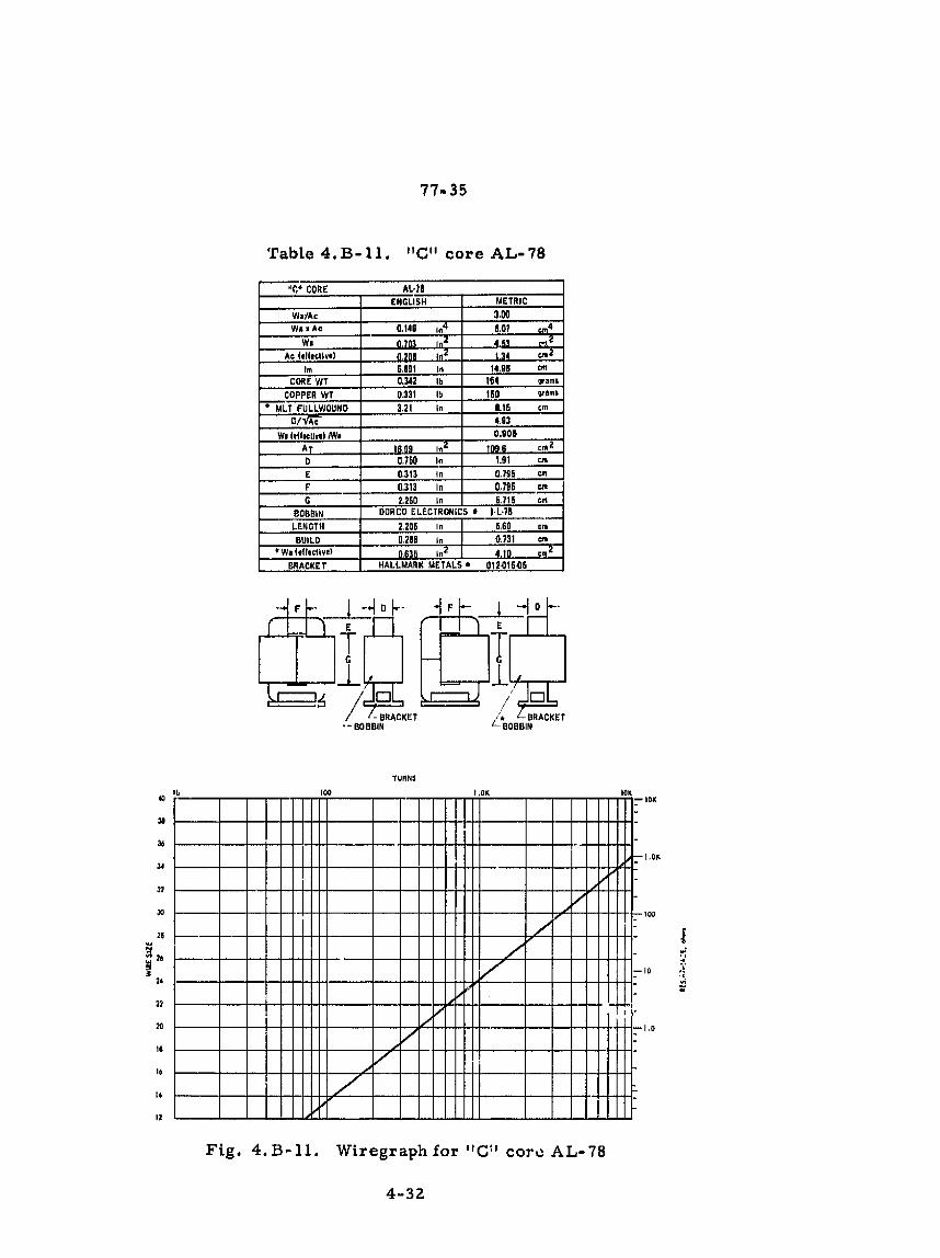
77- 35
Table 4,B-11. "GI1 core AL-78
Fig. 4,B-11. Wiregraphfor l1C:' corr:AL-78
4-32

77- 35
Tablo 4 , B- 12, tiCib core AL- 18
, Ef(fiL, i. I
0 a ' DRACKET r ORACKET
* UOOnlN IIOUUlN
TURNS
Fig . 4.B-12. Wiregraph for "C" core AL-18
4 - 3 3
R E~RoDUCNILI'~'Y rw ~'tifi OBlGlNAL PAGE is .Sm

Fig. 4.B-13. Wiregraphfor "C" core AL-15
4- 34
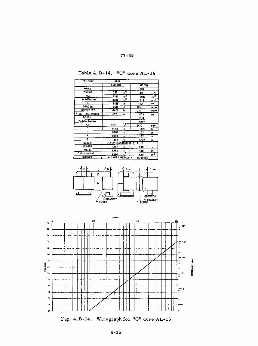
77-35
Tablo 4, B-14, ItC1' core AL-16
TUHNS
Fig. 4.B-14. Wiregraphfor l1C" core AL-16
4-35

77-35
Table 4.B-15. ''CII core AL-1';
TURNS
Fig, 4. B- 15. Wiregraph for "C" core AL.. 17
4- 3 6

77- 35
Table 4.B-16. "C" core AL-19
TURNS
Fig. 4.B-16. Wiregraphfor "CH core AL-19
4-37

77-35
Table 4. B- 17. "C1! core AL-20
. ' / BRACKET ' - BOOBIR
- r - BRACKET BOBBIN
F i g , 4. B- 17. Wiregraph f o r ' IC1' core AL-20
4-38
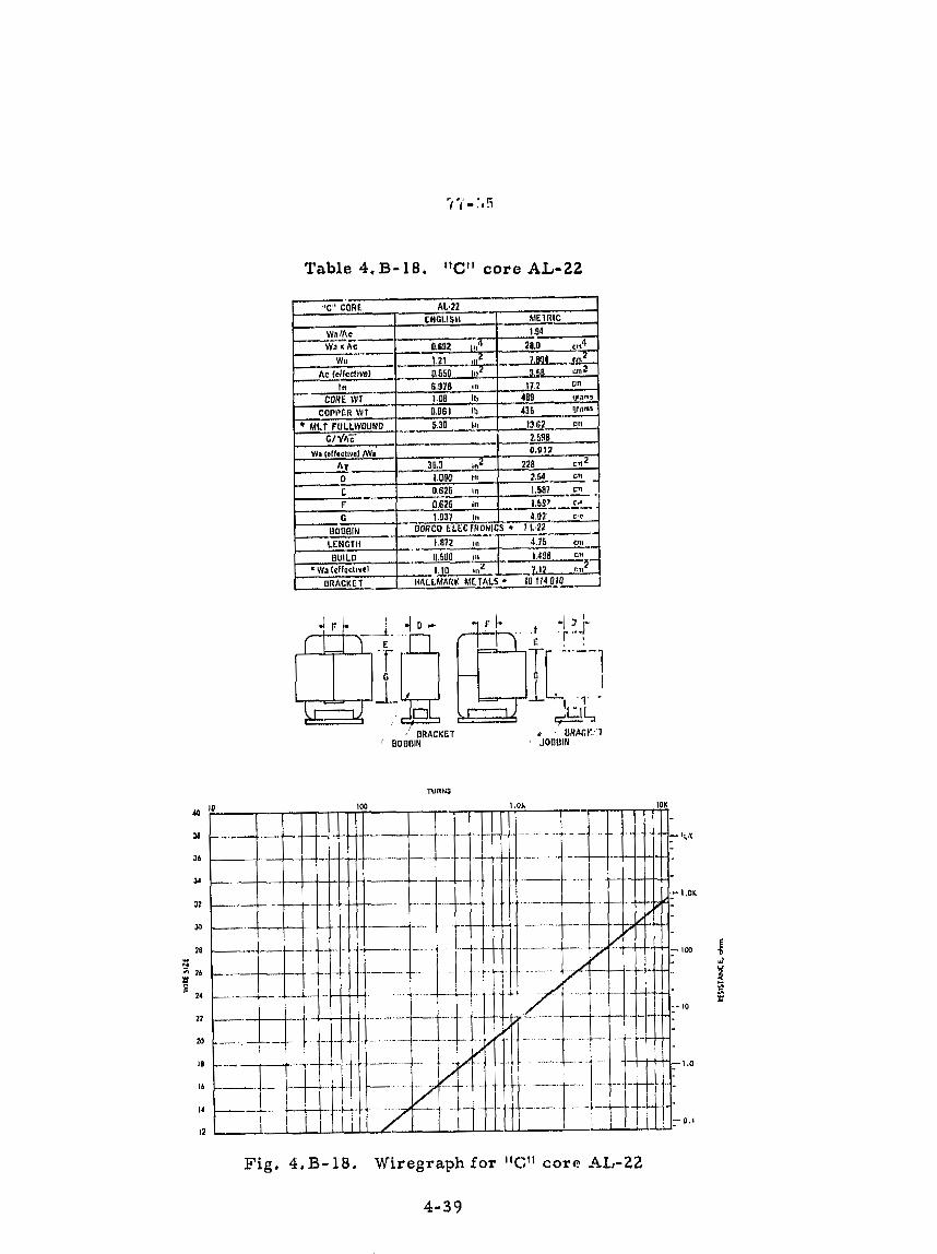
r { l ( - : a 5
Table 4,B-18, I1C" core AL-22
TURNS
Fig , 4, B-18, Wiregraph for ' 'Gtr core -4L-22
4-39

(4-f) f fi, K+
Table 4. B-20. l'C'l core AL-24
(.$ Diii., 6
-1 .. ' 1
-"A 0 0 BRACKET * * IlflhCKET
BOURlN IJ0OUlN
115 - . ~ COHt 14T
COPPtR \VT
' hiLT rULLWOUNO c1vh';-
Wa lrllrc~lvh I W ~ A
Fig, 4.B-20, Wiregraph for tiC1l core AL-24
1811 in--- - - 1.220 111
1601 5 5 76 &
-
r - - 4 3 5 -
70 0 C1"
65? urams - 08 tjflilnlr
I. ,fl? -~ .-
--- ' , l o
- a.oru 211.6 t4''L- - 2 5 4 .,.cm--
1 581 cm I on6 cm 6816 an
L - . -. r C
--- 0 626 411 - o 150 i n
2313 ~n UOUUlN LE"GT'' -- IIUILO-
h W a t t ~ ~ a c ~ ~ v c ~ URACKCt b-
OORCO LLLCCONICS U l L 24 2 248 :n ---- --, 0716 I?
I 801 w2
6 1 0 3 ern -- - - 1 R I ~ tltb
--+_1P37 mZ _ IlhLLMARK hitTALS a 10 200 Dl0

1,000,00011
100,ooon
i0,mn
I ,006n
loon
ion
t n
,otn 1
Fig . 4. B-21. Graph for inductance, capacitance, and reactance
QRIrnAJL P M E 4-42 OF PBOR OYALr

1.0 10
AREA PRODUCT. Ap cm 4
2 Fig. 4. B-22. Area product vs energy
2 B m ' = 1. 2 (tesla)
K = 0.4 u
K- = 395 J

REFERENCES
1 , Molyparmalloy Powclor Cor c s , Catalog MPP-303 5 , Magnetic, Inc. , Butlor, Pa,
2 , Loo, R , , Electronic 'Transformer and Circuits, Second Edition, John Wiley & Sons, New Yorlc, N, Y, 1958,
3 . Sllectron C o r e s Bulletin SC- 107B, Arnold Engineering, Marengo, I l l , , unda tad,
4 , Qrthosil Wound C o r u Catalog No, W 102-C, Thomas & Skinner, Inc. , Indianapol i~ , Ind, , undated,

TOROIDAL POWDER CORE SELECTION
WITH dc CURRENT

Inductors which c a r r y d i r ec t cur ren t a r e used frequently in a wide
va r i e ty of ground, air, and space applications, Selection of the best magnet ic
c o r e for an inductor frbquently involves a t r i a l - and -e r ro r type of calculation.
The design 5: an inductor aleo frequently involves consideration of the
effect of i t s maglietic field on other devices n e a r where i t i e placed, This is
especially t rue in the design of high-current inductors fo r conver turs and
switching regulators used in spacecraf t , which m a y a lso employ sensit ive
magnet ic field detectors . F o r this type of design problem i t is frequently
imperat ive that a toroidal co re be used, The magnet ic flux in a moly-permalloy
toroid (core) can be contained inside the corra m o r e readi ly than in a lamination
o r C type core, as the winding covcra tile core along the whole magnetic path
length.
The author has devvkped a s impl i f ied method of designing optirnurrl
dc c a r r y i n g inductors with moly- p e r m a l l o y ~ ~ p a w d e r ~ ~ , r , ~ ~ ~ ~ ~ ~ T l ~ i s method - .-_ allows the correct c o r e permeabil i ty tb 'be determined ~ i t h ~ u t - ~ i b l ~ r ~ ~
t r i a l and error.
B. RELATIONSHIP OF Ap TO INDTJCTOR'S ENERGY
HANDLING CAPABILITY
According to the ncwly developed approach, the ene rgy -handling
capability of a core is related t o i t s area product Ap:
where:
K cu--ent density coefficier . t(see Chapter 2 ) j
K = window utilization factor ( s e e Chapter 6 ) u
Bm = f lux densitv, t a s l a
Eng = energy, watt seconds
5 -2
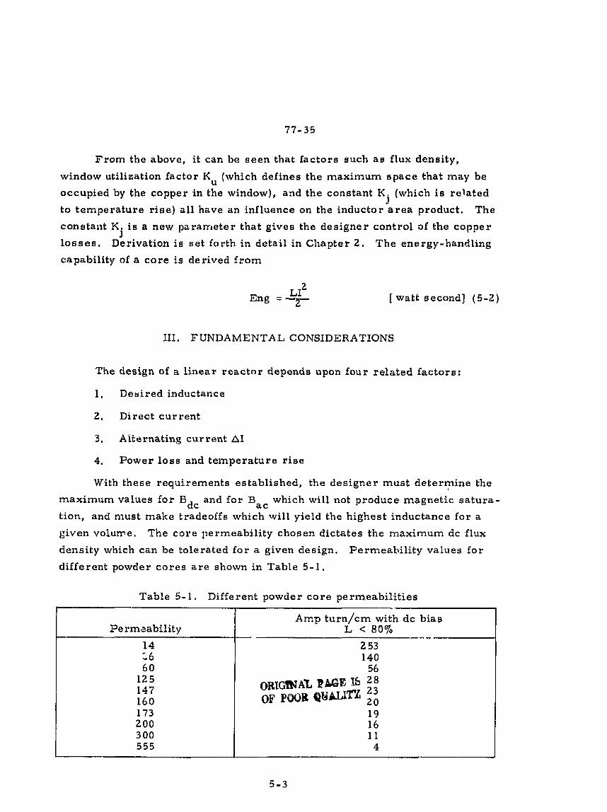
From the above, i t can be seen that factors such as flux density,
window utilization factor KU (which defines the maximum space that may be
occupied by the copper in the window), and the constant K, (which is related 1
to temperature r i s e ) a l l have an influence on the inductor a r e a product, The
constant K , is a new pararr~eter that gives the designer control of the copper J
losses. Derivation is set forth in detail in Chapter 2 . The energy-handling
capability of a core is derived from
L I ~ Eng = -2 [ watt second] (5-2)
111, FUNDAMENTAL CONSIDERATIONS
The design of a linear rcactnr depends upon f o u r related factors:
1. Deaired inductance
2. Direct current
3. A1i;arnating cur rent A1
4. Power loss and temperature r i s e
With these requirements established, the designer must determine the
maximum values for B and for Bat which will not produce magnetic satura- d c tion, and nluet make tradeoffs which will yield the highest inductance for a
given volume, The core permeability chosen dictates the maximum dc flux
density which can be tolerated for a given design. Permeabili ty values fo r
different powder cores a r e shown in Table 5- 1.
Table 5- 1 , Different powder core perm.eabilities
Arr+p turn/cm with dc bias
- L < 80% 2 53 140
5 6 - 4

If an inductancc is to be constant with increasing direct current, there
must be a negligible drop in inductance over the operating current range.
The maximum H, then, is an indication of a care's capability. In tarme of
ampere-turns and mean magnetic path length lm,
H NI [amp turn/cm] (5-3)
'm
NI = 0.8 Hlm [ amp turn ] (5-4)
inductance decreases with increasing flux density and magnetizing force
for various materials of different values of permeability p The selection A * of the correct permeability for a given design is made using equation 5-4
after solving for the area product A * P:
It should be remembered that maximum flux density depends upon
Bdc t Bat in the manner shown in F ig . 5- 1.
-
" Derivation is se t forth in detail in Appendix 5 . b. at the end of this Chapter.
5-4

[teela] (5-8)
Combining Eqs . (5-7) and (5 - a),
A1 0 . 4 ~ N I ~ ~ x 0 . 4 ~ N T ~ 1 0 . ~
- t - - [te ela] (5 - 9) - lm 1 m
OR1aibla P01: Ib POOR QUALITY
Fig.
'dc
5- 1. Flux density versus Idc +
Moly-permalloy powder cores operating with a dc bias of 0,3 teela
have only about 80% of their original inductance, with very rapid falloff at
higher densities as shown in Fig. 5-2,
The flux density for the initial design for rnoly-permalloy powder cores
should be limited to 0 . 2 tesla maximum for Bdc plus Bat, Thc losses in a moly-permalloy inductor due to ac flux density are
very low compared to the steady state dc copper loss . It is then a ~ s u m e d
{.hat the majority of the losses are copper:

r - v . I r r r r r l r-4 1 * T 1 I T V I I - I - 1 - v i r ~ m r .
- - - r -
& loo - i2 - d
0 a 90 - - d Z: - - - p 80- - U - E
*
e 70 - - - - -
5 5 0 ~ -
- - . 1 l - l . I L i l l l l . I , I I 1 l l t
.001 ,01 ,02 .04 ,06 0.1 0.2 0.4 0.6 1.0
POLAR l ZED FLUX DENS I TY, TESLA
F i g , 5 - 2 . Inductance versus dc bias
D. A SPECIFIED P:T;;TL.:N PROBLEM AS A N EXAMP-LE
For a typical design example, assume the following:
( 1 ) Inductance 0.001 5 henry
( 2 ) d c current 2 amperes
( 3 ) 25°C rise
The procedure would be a s shown below.
Step No. 1. Calculate the energy-handling capability from
equation 5-2:
L I ~ Energy = - 2 [watt second]
Energy = 0.003 [watt second]

Step No. 2 . Calculate the area product Ap from equation 5-1:
b e s la]
Af ter the A has been determined, the geometry of the inductor can be P
evaluated as described in Chapter 2 f o r weight, for surface area, and fo r
volume, and appropriate changes made, i f required.
Step No. 3 , Select a powder core from Table 2-2 with a value of A P
closest to the one calculated:
55071 with a n A = 1 . 9 6 6 P
F o r more information, see Table 5. B-6.
Step No. 4. Calculate the current density J from equation 5. A - 19:
ORIGIN& P E E 16 OF POOR Q V A L m

The value for K, is found in Table 2-1: J
J = (403) ( 1 , 9 6 6 ) - 0 , 1 2
Step No, 5, Calculate the permeability of the co re required frorn
equation 5. A-24:
( s c c Table 5.13-6,)
F r o m the manufacturer's catalog, the core that has the same e i z c but has a
permeability cloaer t o the orie calculated is the core 55550, with a permea-
b i l i t y oE 2 6 . This particular core has 28 millihenry per 1000 turns.
Step No, 6 , Calculate the number of turns required for
1. 5 millihenry.
L = inductance
=loo0 = inductance at 1000 turns

Stop No. 7 . Calculate tho hare wire size A w(n):
Step No. 8. - Select the wire area A in Tablo 6 - 1 for equivalent W
(AWG) wire s i z e , column A:
Step No, 9 . Calculate the resietance of the winding, using Tablo 1 1,
colunm C , and Table 2-2 , column 4 , for the MLT:
R = M L T U N X (column C ) X g X [Q I
Step No, 10. Calculate the copper loss:
[watts]
[watt.]
L'rom chapter 7 , th- surface area A t required to dissipate waste heat
(expressed as watts Loss per unit: area) is:

Rcfcrring to Table 2 - 2 , column 2, for the 55071 size core, the strrface area
A~ is 44.7 cm2:
w l ~ i c l ~ wil l produce the required temperature rise,
(Xn a t e s t sample made to prove out this example, the measured inductance
was found to be 0.0015 hy with a resistance of 0.36 ohms at 2 5 O ~ and 0.388 chms
a t 4 5 O ~ . )

BIBLIOGRAPHY
Stan, P4 , Toroid Design Analysis, Electro-Technology, August 1966, Pages 85 -94,
Smith, C. D. , Designing Toroidal Inductors with dc Bias. NASA Tecl~nical Note D-2320, Gaddard Space Flight Center, Greenbelt, Md.
Blinchikoff, H . , Toroidal Inductor Design Electro-Technology. November 1964, Page 42-50.

APPENDIX 5. A
TQROID POWDER CORE SELECTION wIrrr; dt-. CURRENT
After calculating the inductance and dc current, select the proper 2 permeability and size of powder core with a given LI / 2 , The energy-
handling capability of an inductor can be determined by its A prc duct, of * P
which W i s the available core vindow area in omL and Ac is the core a 2 effective cross sectional area in cm . The W,Ac o r area produ-l AD rela-
tionship i s obtained by so lv~ng E = ~ d ~ / d t as f o l l o ~ s : " ~
I rtr = Bm Ac
L I ~ p r Po N~ A; I2 Energy = - -. 2 -
1' 2
m *
Prim!. s indicate measurements in the mks system.

If Bm i s specified,
2
Eng =-
Reducing to
Solving for pA p,,
Substituting into the energy equation,
B; A: KU Wg J' - W6 A; B,JfKu Enp z . 2 - -- - 2. ( 5 , A-14) m m

let
1' = l m m x l o w 2
W; = wa x
A ' = Ac iZ log4
Sf = J X 10 4
S u h ~ t i t u t ~ n g into the energy equation,
Eng = *a *c Bm 2 K~ x
Solving for Wa A=,
and since the area product is
then
Combining the equation from Table 2 - 1,

yielding
88 - 2 (Energy) :# I 0 4
- P K* B I<--- m l
Aftelm the core size has been determined, the next step is to pick the
right permeability f o r that core e i z n . This is done by solving for p in A equation 5 . A - 13.
for p, = 4n x l om7
DRIGNAL PAGE 15 GP POOR QUALITY

APPENDIX 5. B
MAGNETIC AND I31biETJSIONAL SPECIFICATIONS FOR 13 COMMONLY USED MOLY -PERMALLOY CORES
The following remarks apply to each of Tables 5 , B- 1 to 5 , B - 13, the
data in which was conzpilod f rom manufacturers' data.
11) Total weight is core weight plus wire weight assuming AWG 20
( 2 ) Maxirnutn OD of wound core with residual hole = 1 / 2 ID
( 3 ) MI,T ( n c a n lcngth/ turn) full wound toroid
(4) Effective window area W a ( o ~ i ) = 3nr2/4
Gibaphs (Figs . 5 . B - 1 to 5 . B-13) rolatc to the 13 different core s i z o s ,
T h c graphs shnw rcsjstance, number of turns , inductance and wire s i z e For a
window utilization factor of 0 . 4 0 , and are based on a permeability of 6 0 . To
convert for other permeability values, llle appropriate inductance multi-
plication factors l i s ted should be used. Ti l e info rnlation appearing in the
tables and sn the figures wi l l enable the engineer to arrive at .A close
approximatiox1 for breadboarding purposes.

l'ablc 5. 13- 1. 1l)iitirnsional specifications for hlagnctic Inc 5 5 0 5 1 -A2 , A rnolcl I*31ginccring A-051 027-2
Fig
3 h I a q m l 13 01 t 1 , % 4 . , l > 1 4 s d b m i 1 1 4 1 , 7 1 1 i' 1 I I'
rNnt% IWi -11 I"
5. B-1. W i r e and induc,katlce graph for Core 55051
5 - 1 7

Table 5. A - 2 . Dimaxlsionai specifications f o r Magnetic Inc 5512 1 -A2 , Arnold Engineering A -266036 -2
Fig . 5. B-2 . W i r e and inductance graph f o r Core 5512 1 -A2

Table 5. B-3 . Dimensional specifications for Magnetic Inc 55848-A2, Arnold Enginoe ring A-848032,-2
Fig . 5 .B-3, W i r e and inductance graph for Core 55648-A2
5- 19

Table 5 . B-4. Dirncneional specifications fo r Magnetic Inc 55594-A 2 , A rnold Engineering A-059043 -2
Fig. 5. B - 4 . W i r e and inductance g r a p h for Core 55059-A2

Table 5. B-5. Dimensional specifications for Magnetic Inc 55059-h2, Arnold Engineering A-894075-2
F i g .
I WOUND OD MIN MLT
A, SURFACE AREA
PLRMEAUILITY
p 125
# I60 Lc ZOO
Lc 550
1. 191 in
1,HI In
.I 18 in2
1.01 a r t
I , 1 cnl
ZH 32 m2 bO
2.08 r: I t n /-I bO
2,67 x L 6- C( 60
3 ,33 r L m II 60
9.17 r L n L c 60

Table 5 , B-6 , Dirnenoional specifications for Magnetic Inc 55071 -A2, Arnold Engineering A-29 106 1 -2
Fig, 5.B-6. W i r e and inductance graph for Core 55071-A2
5-22
WOUND OD hllN
MLT A, 7 SURFACE AREA
PERMEABILITY -- P 125
Y 160
P 200 /I 550
I , .IBb It1
1.89 In
4 ,189 l r l Z
7 a n
4. $0 an
40, b8 cm2
60
2.08 r L a. C1 60
2.67 1 L (.t L( 60
3.33 x L nt 11 60
9.17 K L wsP 60

Table 5, B-7. Dimensional specifications f o r Magnetic Inc 555861A2, Arnold Engineering A -345038-2
Fig.

Table 5, B-8 . Dimensional specifications for Magnetic 55076-A2, Arnold Engineering A -076056 -2
ORIGINAL C U E Ib OF POOR QWAldv
Fig. 5. B-8. W i r e and inductance graph for Core 55076-A2
5-24

Table 5 , B-9 , Dimensional specifications for Magnetic Inc 55083-A2, Arnold Engineering A-083081-2
Fig. 5 . B-9. W i r e and inductance graph for Gore 55083-A2
WOUND OD MIN
hi L T A, S U R F ~ C E AHEA
PEAMEAUILITY
jl 125
CI 1bO
f l ZOO
jl 550
I , 7l1 in
2,11. 1t1
q..Ih 2
---
.! , '8 -I cnt
6,07 cm
I . cln2 1 60
2.08 x L n f l 60
2.67 K L $'- UAO 3.33 x 1.- V 40
9.17 h L 0 U 60

Table 5. B- 10. Din~ensional spccificatione for Magnetic Inc 55439-A2, Arriold Engineering 4-75913 5-2
Fig. 5 . B-10. W i r e and inductance graph for Core 55439-A2
WOUND OD hllN hlLT
A, SURFACE AREA
I'ERMEABILITY
Jl 125 - .- - Ir 160
f l 200
550
L. 04 in
3. OD III
12. 111 i n 2
5 , I ? cm 7. br! cm
70. 17 01
60
2.08 r L * p 66 . -.- 2.67 x I. <.' jJ 60
3.33 r L . ~ 1 1 6 0
9.17 x L w P bO

Table 5, B - l 1, Dimensional specification6 for Magnetic Inc 551 10-A2, Arnold Fligineering A-488075-2
F i g . 5. B-11. W i r e and inductance graph for Core 551 10-A2
5-27

Tablo 5 , B-12. Dimensional ~;pccifications fo r Magnetic Inc 55716-A2, A mold Engineering A - 106073 - 2
Fig. 5. B-12, W i r c and inductance graph fo r Core 5571
t METRIC
( J . DL
I h In'l 9. 32, . . cm
5. I 7 ~m
1. UI1 CI
1.435 cm
7,6C em2
6 L cir
1 . 2.1 C F
1 ~ ~ 7 3 cnl
l l5 gram5
L11i2 gt imr
5, 8.2 m b . 5 0 CHI
9 I . l Z cm2
0 0
2,08 r L II 60 2.67 x ', w1 II 60
3.33 x L c P 40
9.17 r LwlP 60
- , EMGL15H
1Va'Ac
W r A6
- 2D--, ID - I I T _
\VJ WINDOW AREA
wa EFFECTIVC A r CROSS SECTION
- ~ m PATI! L E ~ I O ~ I ~ COHE WEIGIIT --
?TnL WEIGIIT
=hi"Dii MI N --- T
A, SbRFACE AREA
PERMElrDILlTY
CI 125 ---. /J 160 f l 200
U 550
-F 2.035 In
I , 210 in
0, $65 In 1, .IR * I O ~ CIR-MIL
0.87.0 ill2
0. l ')d in2
5.02 ~n
0. 290 111
0. 1 5 2 Ib
2 . 2%) in
2 . 5 5 dn
I ln2

Table 5 . B- 13. Dimensional specifications fo r Magnetic Inc 55090-A2, Arnold Engineering A-090086-2
Fig.

CHAPTER VI
wmaow UTILIZATION FACTOR K~

A . IN TRODUC TION
The window utilization factor is the amount of copper that appears in the
window arca of thc transformer or inductor, The window utilization factor i s
infl~lenccd by 4 different factors: ( I ) wire insulation, (2) wire lay (fill factor),
( 3 ) bobbin arca (or, when using a toroid, the clearance hole for passage of the
shuttle), and (4) insulation required for multilaycr windings or between windings.
In the design of high-current or low-current transformers, the ratio of conductor
area over total wire area can vary frum 0.941 to 0 . 6 7 3 , depending on the wire
size. The wire lay or f i l l factor can vary from 0.7 to 0 . 5 5 , depending on the '
winding technique. The amount and the type of insulation are dependent on the
voltage.
B. WINDOW UTELIZA TION FAGTOR
The fraction Kll o f the available core window space which will be occupied by the winding (copper) is calculated from areas S 1 ' S2, Sg , and S4:
where
- conductor area s1 - wire area
- woundarea - '2 usablewindowarea
- usable window area s3 I window area
- - usable window area '4 usable window area C insulation area
in which
conductor area = copper area
wire area = copper area + insulation area ORlGENAL t&GE Xb OF POOR Q11AWn
wound area = number of turns x wire area of one t w r i

ueable window area = available window area minus reaidual area which result8 from the particular winding technique used
window area = available window area
insulation area = a r e a usable for winding insulation
S is dependent upon wire size. Col:amns A and D of Table 6- 1 1
may be used for calculating some typical values such as for AWG 10, AWC 2 0 ,
AWG 30 and AWG 40,
Thus :
AWG 20 = i; ,065 crn
0 * 5 0 6 7 = 0 , 7 4 7 ; and AWG 30 = 0.6785 crn
0 . 048,:~ cm 2 AWG 40 = 0, 0723 o m d = 0.673 ,
When designing law-current t ransformers , it is advisable to reevaluate
S because of the increased amount of insulation, 1
S2 is the f i l l factor for the usable window a r e a , It can be shown that for
c i rcu lar cross-sect ion wire wound on a flat form the rat io of wire area to
the a r e a required br tho turns can never be g rea te r than 0,91. In practice,
the actual maximum value is dependent upon the tightness of winding, var ia-
tions in i i l su la t io~~ thickness, and wire lay, Consequently, the fill factor is
always l ess than the theoretical maximum.
As a typical working value fo r copper wi re with a heavy synthetic film
insulation, a rat io of 0.60 rnzy be safely used.
The te: n S defines how much of the available window space may actually 3 be used for the winding, Tbe winding a r e a available to the designer depends on
the bobbin configl~ration. A single bobbin design offers an effective a r e a W a
between 0,835 to 0.929 while a two bobbin configuration offers an effective area
Wa between 0.687 to 0.872. A goad value to use f o r both configurations is 0.75.

Whcn designing with a pat core, Sj has to be reduced because the effective
Wa var ies between 0.55 and 0.71.
The t e rm S4 defines how much of the usable window space i s actually
being used for insulation. If the t ransformer has multiple secondaries having
significant amounts of insulation S4 should bc reduced by 10% fo r each additional
secondary winding because of the added space occupied by insulation and partly
due to poorer space factor.
A typical value for the copper fraction in the window area is about 0.40,
Far example, for AWG 20 wire, S 1 x S2 X S j X S4 = 0.855 X 0.60 X 0.75 X
1.0 = 0 , 3 8 5 , which is very close lo 0.4,
This may be stated somewhat differently as:
C , CONVERSION DA TA FOR WIR,E SIZES FROM # l o t o #44
Columns A and B in Table 6 - 1 give the bare area in the com~nonly used
c i r cu la r mils notation and in the met r ic equivalent for each wire size, Column - 6 C gives the equivalent resis tance in microhms/cent imeter (@/cm or 10 a/ cm. ) in wire length fo r each wire size. Columns D to L relate to coated wires
showing the effect of insulation on size and the number of turns and the total
weight in grams/centirneter,
The total resis tance for a given winding may b e claculatecl by multiplying
the MLT (mean lengthlturn) of the winding in cent imeters , by the rnicrohrns
crn for the appropriate wire s ize (Column C), and the total number of turns.
Thus
R = (MLT) X (N) X (Column C) X C X l o m 6 [ohms]
For resis tance correct ion factor L; (Zeta) for higher and lower temperature,
see F i g u r e 6 - 1 .

Table 6-1, Wire table
.fb(r &la Isom REA M.sartlc WIca Ddd.alor (Rmf. I ) .
amh310m .mas. the matry II tho column muat bm multl>li.d by 10-1

TEMPERATURE OC
BASED ON TEMPERATURE COEFFIC f ENT
-30 OF 0,00393 ADOPTED 5 STANDARD BY THE INTERNATI CNAL ELECTROl
-40 CHEMICAL COMMISSION IN 1913
-so0 c
Fig . 6-1. Resistance Corrcction Factor 5 , Axeta) for wire resistance at temperatures between -50 and 1 0 0 ~ ~
The weight of the copper in a given winding may be calculated by multi-
plying the MLT by the grams/cm (Column L) and by tlze total number of turns.
T11us
Wt = (MLT) X (N) X (Column L) [grams]
6 -6

'rums per square inch and turns per equare cm are based on 60% wire fill
f ac to r . Mcan longth/turn for a given winding m a y be calculated with the aid of
Fig. 6-2, Figure 6-3 shows a t ransformer bcinu constructed using layer insula-
tion. When a t ransformer is being built in th ie way, Table 6 - 2 and 6-3 will help
the dc eigner find the cor rcct insulatLon thickness and margin for thc appropriate
wire size.
D. TEMPERATURE CORRECTION FACTORS
Tho rcs i~ l tance values given in Table 6 - 1 a r e based upon a te-nperature of
2 0 O ~ . For othcr temperatures the cffcct upon wire rc s i s tancc tag bbc calculated
by multiplying the resietancc value for the wirc size shown in column C of
Table 6 - 1 by the appropriate correct ion factor shown on the graph, Thus,
Correc ted Resistance = p ~ / c m (at ZOOC) x 5 .
E, WINDOW UTILIZA TION FACTOR FOR A TOROD
Thc toroidal magnetic component has found wide use in industry and aero-
space bccause of i ts high f rcquency capability. The high frequency capability of
the toroid is due to its hifill ra t io of window a r e a over corc c r o s s section and its
abi l i ty to ~ecomrnoda te different s tr ip thickness in its boxed configuration.
Tape strip t h i ckness is an important consideration in selecting cores . Eddy-
current losses in the core can bc reduccd at higher frequencies by use of thinner
strip stock. The high ratio of window area over core c r o s s section insures the
lnininlum of iron and large winding area to minimize the flux density and c o r e
10s s . The magne t i c flux in the tape wound toraid can be contained inside the
corc more readily than in lamination o r C type core as the winding covers the
corc along thc wl~ole magnetics path Length which gives lower electromagnetic
interference.
The toroid does not give a smooth A relationship as lamination, C core , P
powder cores and pot cores with respect to volume, weight, surface area ?.nd
current dcnsity as can be eaen in Chapter 2. This is because tlzo actual core
is always embedded in a case having a wal l t l~ickness which has no fixed rela-
t i o n t o t h e a c t u a l c o r e a n d omesre la t ive ly larget l~esmal ler theactua lcore onlcm AlJ I?B OF pwB Q * ' ~ ~
6 -7

(MLTI2 = (MLT)I + (al+a2+2cl OR
(MLf = 2(rk2J) + 2 ( r t 2 J I +I [ ~ ( i ~ ~ + a ~ + , . . + u ~ - ~ ) + a,,]
WHERE:
q BUILD OF WINDING 61 a2 = BUILD OF WINDING 62 a,, = BUILD OF WINDING Iln c = THICKNESS OF lNSU LATION BETWEEN al & a2
Fig . 6-2. Computation of mean turn length

LAYER INSULATION WIRE TUBE
MARG l N
Fig. 6 - 3 , Layer insulated coil
Table 4 - 2 . Laycr insulation vs AWG
WINDOW AREA
Insulation thiclrna s s
AWG
cm inch - -

Tatlc 6 - 3 , ~ i r & i n vs A W C
Margin - - A WG.
cross section is. I'hc available wir~dow area insiclc Llrc case, therefore, i s not
a f i x c d percentage of the window area of the uncasecl core,
Design Manual TWC-300 of MAGNETICS, h c . indicates that: random
wound cores can be produced with fi l l factors a s high as 0 . 7 , but that pragres-
sivc sccior wound cores can be produccd wit11 fi l l factors of only up to 0 . 5 5 .
As a lypical working value for copper wire wit11 a hcavy synllletic f i lm insula-
tion, a ralio of 0.60 may be uscd safely, Figure 6-4 is based upon a f i l l factor
ratio of 0 . 6 0 for wire s izcs 14 1hrough 42 wit11 0. 5 1. 3 , remaining.
2 2 2 The term usablc window cm /window crn (.. 3 ) defines how much of the
available window space may actually be used for the winding. Figure 6 - 5 is
based on tho assumption that the inside diameter (ID) of the wound core is one-
half that of tho bare core, i, e, , S3 = 0 . 7 5 (to allow free passage of the shuttle).
Insulation factor (54) in Figure 6 -4 is 1.0; this docs not take into
account any insulation. The window utilization factor (KU) is highly influenced
by the ins~lat ion factor (S4) because of the rapid build-up of insulation in a
toroid as shown in Figure 6 - 6 .
It can be seen in Figure 6 - 6 the insulation builc? up is greater on the
inside than on the outside. For an example in Figure 6 - 6 if 1.27 cm wide tape
was to be used with an overlap of 0 , 32 c;n on the 0, D, the overlap thickness

TURNS
Figure 6-4. Toroid inside diameter versus turns

EFFECT I VE WINDOW AREA
, ~ 1 1 , ~1~ - 4"-
Figure 6-5, Effective winding area of a toroid
Figu. re 6-6 . Wrap toroid
6 - 12

wovld bc four times the thickness of the tape. It wil l be noted that the amount
of overlap will depend greatly on the size of the toroid. As the toroid window
gets smaller the over-lap increa~res. There is a way to minimize the build on
a wrapped toroid and that is to uee periphery ineulation a s s l~own in Figure 6-7. The uec of periphery insulation minimizes the inside diameter overlay a s shown
Figure 6-8.
PERlf:iiRY INSUI,ATlON
WOUND TOROlD
GATHER
Figure 6-7. Periphery insulation
PERIPHERY INSULATION - TAPE OVERLAP - INSULATING TAPE
@~@~NAL Pff iE B f31i\ PwR QUALITY
Figure 5 -8 . Minimizing toroidal inside build

Whcn a clcaign rcquircs a multitude of windings, all of which have tu bo
insula tcd, tllcn lhc insulation factor (S ) becomes very imporlant in the window 4 utilization factor For cxamplc, a low current toroidal transformer with
insulation has a significant influence on tile window utilization Sac tor as 7,. l v ~ ~ t
bclaw:
S1 2 140 AWG 1% S1 X S2 X Sj X S4
Tabtc 6-4 was gcncrated as an aid .dor tho engineer; it is a listing of
29 A. I. E. E. prcfcrred tapc~wound toroida" -ores with rnclric dimension. The
powcr handling capabiliiy is listed in I;kc last column undcr A nro 1 ,broduct. P


CHAPTER VII
TRANSFORMER - INDUCTOR
EFFICIENCY, REGULATION, AND TEMPERATURE RISE

A.. INTRODUCTION
Transfarmer efficiency, regulation, and temperature r i ~ e are all
interrelated. Not all of the input power to the transformer i a delivered to the
load, The difference batween the input power and output power ie converted into heat. This power loss can be broken down into two components: core loea
and copper loss. The core loss i a a fixed lose, and the copper loss is a
variable loss which i d related to f i e current demand of the load, Copper loss
goes up by the square of the currant and is termed quadratic loss. Maximurn efficiency is achieved when the fixed loss is equal to the quadratic a t rated
load. Transformer regulation is the copper loss P, divided by the output
power Po.
B, TRANSFORMER EFFICIENCY
The efficiency of a transformer is a good way to measure the effective-
ness of the design. Efficiency is defined as the ratio of the output power Po to
the input power Pin. The difference between the Po and the Pin is due to
losses. The total power loss in a transformer is determined by the fixed
losses in the core and the quadratic losses in the windings or copper. Thus
where Pfe represents the core loss and P represents the copper loss. CU
Maximum efficiency i s achieved when the fixed loe s is made equal to the
quadratic loss a s shown by equation 7-1 1. Transformer loss versus output
*load current i s shown in Figure 7- 1.
The copper loss increases as the square of the output power multiplied
by a constant K which ie thus:

12
COPPER LOSSES 7 6 - 4 - ' FIXED LOSSES 2
OUTPUT LOAD CURRENT, %
Fig, 7- 1, Transformer loss versus output load current:
which may be rewritten a s
Since
and the efficiency is
then

and, differentiating with respect to Po:
Pfe + PO + = 0 for max q
C . RELATIONSHIP OF A TO CONTROL OF TEMPERATURE RISE P
1. Temperature Rise
Not 611 of the P input power to the transformer i s delivered to the load in
as the Po. Some of the input power i s converted to heat by hysteresis and eddy -
currents induced in the core material, and by the resistance of the windings.
The first is a fixed loss arising from core excitation and is termed Itcore loss, ' 1
The second is a variable loss in the windings which i s related to the current
demand of the load and thus varies as I ~ R . This is termed the quadratic or
copper 10s s,
The heat generated produces a temperature rise which must be con-
trolled to prevent damage to o r failure of the windings by breakdown of the
wire insulation at elevated temperatures. This heat is dissipated from the
exposed surfaces of the transformer by a combination of radiation and con-
vection. The dissipation is therefore dependent upon the total exposed surface
area of the core and windings.

Ideally, maximum efficiency is achieved when the fixed and quadratic lossae are equal, Thu1~:
and
When the copper lose in the primary winding i~ equal to the coppnr loaa in the aecondary, the current density in the primary is the same as the cur- rent density in the secondary:
and
Then
If?. J, .J JP = ,+ = Wa
+ 2 . Calculation of Temperature Riee
Temperature rise in a transformer winding cannot be predicted with complete precision, despite the fact that many different techniques are
described in the literature for its calculation. One reasonably accurate

method for open core and winding construction is baaed upon the aesumption that core and winding lossea m a y be lumped together as:
and the assumption is made that thermal energy is dissipated uniformly through-
out the surface area of the core and winding aseembly.
Transfer of heat by thermal radiation occurs when a body is raised to a -- temperature above its surroundings and emits radiant energy in the form of
waves. fn accordance with the Stefan- Boltzmann law, * this may be expressed as:
in which
Wr = watts per square centimeter of surface
K = 5.70 X 10⁻¹² W cmm2 ( o K ) - ~ r
= emissivity factor
T2 = hot body temperature in degrees kelvin
T1 = ambient or surrounding temperature in degrees kelvin
Transfer of heat b y convection occurs when a body is hotter than the sur-
rounding medium, which usually is air. The layer of air in contact with the hot
body which is heated by conduction expands, and rises, taking the absorbed
heat with it. The next layer, being colder, replaces the risen layer, and in
turn on being heated also rises, Thia continues as long as the a i r or medium
surrounding the body is at a lower temperature, The transfer of heat by con-
vection is stated mathematically as :
*Reference 2, Chapter 3.

in which t
W, = watt8 1088 per square centimeter
F = air friction factor (unity for a vertical eurface)
8 = temperature rise, degree0 C
p = relative barometric pressure (unity at sea level)
'I = exponential value ranging from 1.0 to 1.25, depending on the shape
and positian of the surface being cooled.
The total heat dissipated from a plane vertical surface i a expressed by
the a w n of equations 7-18 and 7-19:
3 . Temperature Rise Versus Surface Area Dissipation
The temperature rise which m a y be expected for various levels of power
loss i s shown in the monograph of Figure 7-2 below. It is based on equa-
tion 7-20 relying on data obtained from Reference 2* for heat transfey effected
by a combination of 55% radiation and 45% convection, from surfaces having an
ernissivity of 0.95, in an ambient temperature of 25 "C , at sea level. Power 2 lose (heat dissipation) is expressed in watts/cm of total surface area. Heat
dissipation by convection from the upper side of a horizontal flat surface is on the order of 15 to 207'0 more than from vertical surfaces, Heat dissipation
from the underside of a horizontal 0.at surface depends upon surface area and
conductivity,
%see References in Chapter 3.

VI
LMtSSlV l lY 0.95 4% C O N M C I I W 5% RAOlATlON
0+001 L L 1 1 4 s L I ~ I r 1 r 1~
lo0 c lo@ C
Af * lEMPERAtURE RISE, OLGRLES C
Fig, 7-2, Temperature rise versus surface disaipation
4 . Surface Area Required for Heat Diesipation
The effective surface area At required to dissipate heat (expressed aa
watts dissipated per unit area) is:
in which iTc ie the power density or the average power dissipated per unit area
from the surface of the transformer and P is the total power lost or r: dis sipated.
Surface area At of a transformer can be related to the area product A
of a transformer, The straightline logarithmic relationship shown in Fig- P
ure 7-3 below has been platted from the data shown in Table 2-5, Chapter 2.

Fjg, 7:3, Surface area versus area product A P
From this, the following relationship evolves:
and (from Fig, 7-2)
'Y = 0.03 w/cmZ at 25'C riea (7-23)
Figure 7-4 utilizes the efficiency rating in watts dissipated in terms of
two different, but commonly allowable temperature rises for the transformer
ovur ambient temperature, The data presented are used as bases for deter- 2 mining the needed transformer surface area At (in crn ),

Fig, 7-4, Surface area var:?,rts total watt loss for a 2 5 O r j and 50'C rise
D, REGULATION AS A FUNCTION OF EFFICIENCY
The minimum size of a transformer is usually determined either by a
temperature rise limit, or by allowable voltage regulation, assuming that size and weight are to be minimized,
Figure 7-5 ahows the circuit diagram of a transformer with one second-
ary. Note that u = regulation (70).
Fig. 7-5 . Transformer circuit diagram

The analytical equivalent i n shown in Figure 7-6,
Fig. 7 -6. Transformer analytical equivalent
This assumes that distributed capacitance in the secondary can be
neglected because the frequency and secondary voltage ar o not excessive high. Also the winding geometry ie ~ee igned to limit the leakage inductance to a level
low enough to be neglected under most operating conditions.
Trantt former voltage regulation can now be expressed as:
in which Vo(N. L. ) ie the no load voltage and Vo(F. L. ) ~ E I the full load voltage.
The output voltage computed using Figure 7-5 is:
For the usual condition of

Vo simplifies to
For equal window artiae allocated for the primary and eecondary wind- 2 ings, it can be shown that N R = R..
P
For simplicity, let
At no load (N. L. ) Ro approaches infinity, therefore:
Vo (N.L.) NE
This shows that regulation is independent of the transformer turns ratio.
2 For regulation as a function of copper losa, multiply equation 7-31 by lo:

then
Pin - Pcu + Pya + Po
For regulation as a function of efficiency,
By definition
Solving for Pcu + Pfe
For efficiency as a function of regulation, multiply both sides of the equation
by (1 f 'I):

Solve for q
E. DESIGNING FOR A GIVEN REGULATION
1. Transformars
Although most transformere are deeigned for a given temperature rise, *< they can also be designed for a given regulation, The regulation and power -
handling ability of a core is related to two constante:
LY = Regulation (%)
The constant K is determined by the core geometry which m a y be related by l3
the followfing equation:
The constant Kg i s determined by L e magnetic and electric operating conditions
which m a y be related by the following equation:
The derivation of the relationship for K and Kg i a given at the end of this g
chapter.
* ~ e f erence

Tllc area product A can be ralated to the Cora geometry K in tho P g
following aquation:
Tho derivation is given in datail at tlae end of this chapter.
Rewriting aquation 7-44,
Figura 7-7 shown how area product A varies as a function of regulation, in P
percent.
REGUAflON, a, 9L
Fig. 7-7. Area product versus regulation
7-15

Figure 7-8 shows how weight Wt varies ae a function of regulation, in
percent.
REGULATION, a , %
Fig. 7- 8 . Weight versus regulation
2 . Inductors
Inductors, like transformers, are designed for a given temperature rise.
They can also be designed for a given regulation. The regulation and energy
handling ability of a core is related to two constants:
cr = Regulation (70)

The corrstant K is determined by the core geometry:
- Wa A: ICU
Kg MLT
The constant Ke is determined by the magnetic and electric operating conditions :
The derivation of the specific functions for K and K is given at the and of g e
this chapter,
3 . Transformer Design Example I
For a typical design example, assume an isolation transformer with the
following specifications :
(1) 115 volts
( 2 ) 1 .0 amperes
( 3 ) Sine wave
(4) Frequency 6 0 Hz
( 5 ) Regulation cr 270
The procedure would then be as follows:
S t e p No. 1. Calculate the output power:
Po = VA
Po = (115)(1.0)
Po = 115 [watts]

Step No, 2 , Calculate the electrical conditions from equation 7-46:
Step No, 3, Calculate the core geometry from equation 7-44:
Step No. 4. Select a lamination from Table 7.B-2 with a value K closest g
to the one calculated:
EI - 150 with a K = 35.3 g
Step No. 5 , Calculate the number of primary turntl using Faradayts law,
equation 3 , A - 1 :

The iron cros. eection Ac i a found in Table 7. B -2:
N = 275 turns
Step No. 6 . Calculate the effective window area Wa(etf):
A typical value for Sg is 0.75, a5 shown in Chapter 6.
Select the window area Wa from Tabla 7. B-2 for EI 150:
Wa(eff) = (10.9(0.75)
Wa(sff) = 8,175
Step No, 7, Calculate the prhngry winding area:
Primary winding area = Secondary winding area
Wa eft Primary winding area I 2 2
8.175 Primary winding area = - 2
Primary winding area = 4.09

Step No. 8. Calculate tire wire area Aw with inadation, using a fill
factor S2 of 0.6:
Step No. 9. Select the wire area A, with insulation in Table 6 - l for equivalent (AWG) wire size column D:
AWG No, 18 = 0.009326
The rule i s that when the calculated wire size does not fall close to those listed
in the table, the next smaller size should be selected.
Step No. 10, Calculate the resistance of the winding using Table 6 - 1,
column C, and Table 7 . B - 2 for the MLT:
R = MLT x N x (column C ) x lod6
OF POOR QEl
Cs23

Step No. 1 I. Calculate the copper loor P, and the regulation;
4 , Transformer Design Example XI
For a typical de~lign example, assume a filament traneformer uding a
C core:
(1) 120'voltinput
(2) 400Nz
(3) Sine wave
(4) 6.3 volt output
( 5 ) 5.Oarnpereoutput
( 6 ) Regulation ru 1.070
The procedure would then be as follows:
Step No, 1, Calculate the output power:
Po = VA
Po = (6.3)(5)
Po = 31.5 [watts]
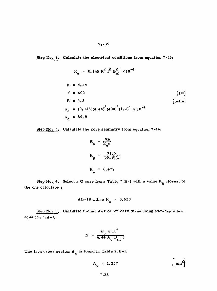
Step No. 2. Calculate the electrical conditione from equation 7-462
Step No, 3, Calculate the core geometry from equation 7-44:
Step No. 4. Select a C core from Table 7 ,B-1 with a value K closest to g
the one calculated:
AX.,-18 with a K = 0.530 I3
Step No. 5. Calculate the number of primary turns using Faradayta law,
equation 3.A-1,
The iron cross section Ac i s found in Tabla 7. B- 1:
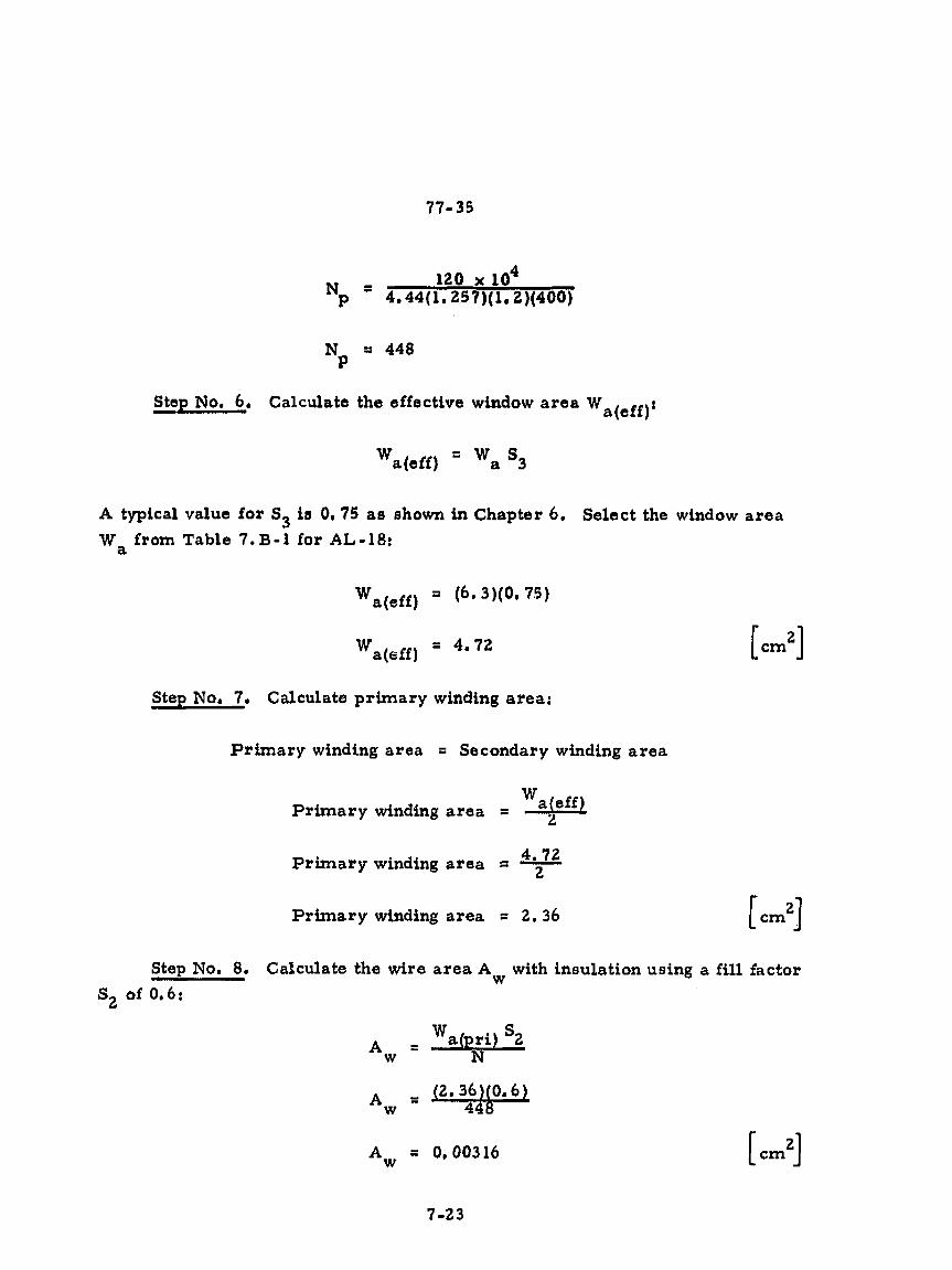
Step No. 6 . Calculate the effective window area Wa(eff):
A typical value for Sg is 0.75 a8 ehown in Chapter 6. Select the window area
W, from Table 7. B - l for AL-18:
Step No. 7. Calculate primary winding area:
Primary winding area Secondary winding area
Wa eff Primary winding area =
4 72 Primary winding area = -?-- 2
Primary winding area = 2 . 3 6
Step No. 8. Calculate the wire area Aw with insulation using a fill factor S2 of 0.6:

Step No. 9. Select the wire area Aw with insulation in Table 6 - 1 for ecluivalent (AWG) wire -128, column D:
AWG No, 23 = 0.003 135 [ cm21 The rule i~ that when the calculated wire size docs not fall close to those listed in the table, the next emaller size should be selected.
Step No. 10. Calculate tha resistance of the primary winding, uafng Table 6-1 , column C, and Table 7 * B - 1 lor the MLT:
Step No. 11. Calculate the primary copper loas Po:
[watts]

Step No,. 12, Calculate the racondary turns;
Step No. 13. Calculate the secondary wire area Aw with insulation using
a f i l l factor S2 of 0.6:
Step No. 14. Silect the secondary wire area Aw with insulation in Table b-1 fur equivalent (AWG) wire size, column D:
AWG No. 10 = 0 ,0559 [m2' ..I
The rule is that when the calculated wire siee doe8 not fall close to ffiose listed
in the table, the next smaller siee should be selected.

Step No, 15. Calculate the resistance of the eecondary winding ueing -- Table 6-1, column C, and Table 7. B-1 for the MLT:
Rg = MLT x N Y (columnC) x
Step No. 16. Calculate the copper loss PcU:
*cu = 0. ?,48
Step No. 17. Calculate the regulation:
5 . Inductor Design Example
For a typical design example, assume:
( 1 ) Inductance = 0.05 henry
(2) C:~.tput power Po = 200 watts
[watts]
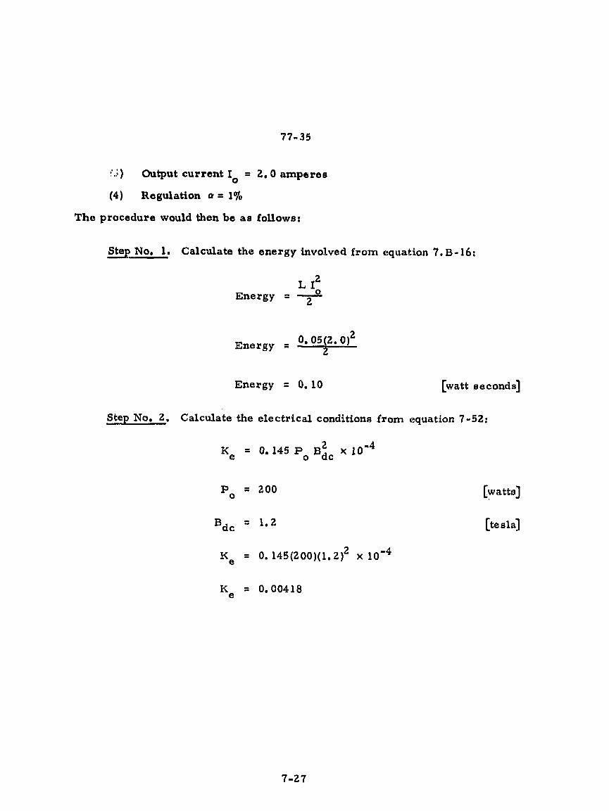
) Output current I. = 2.0 amperes
(4) Regulation rr = 1%
The procedure would then be as follows:
9 No. 1. Calculate the energy involved from equation 7, B- 16:
L l2 0 Energy = - 2
Energy = 0.05(2. 012 2
Energy = 0. lO [watt seconds]
Step No. 2, Calculate the electrical conditions from equation 7-52:
Kg = 0.145 Po B : ~ x lom4
Po = 200
Bdc = 1.2
Ke = 0.145(200) (1 .2)~ lom4
K = 0,00418 e
[watts]
[te~la]

Step No, 3. Calculate the core geometry from equations 7-50: 4
Step No. 4, Select a C core from Table 7 . B - 1 with a value K closest to 6
t?le one calculated:
AL-20 with a I< = 2.32 1
Also select the area ptoduct A for this C core from Table 2 - 6 : P
Step No, 5. Calculate the current density from area product equa- Lion 4.A-18:
J = 2 (Energy) x la4 Bm Ap
Insert values, I< 0.4, u

Step No. 6 . Determine the bare wire size A,. r
Step No. 7. Select an AWG wire size from Table 6-1, column A. The
rule is that when the calculated wire size does not fall close to those lieted in the table, the next smallor size should be selected.
AWG 17 = 0.01038 [ cm21 Step No. 8. Calculate the effective window area Wa(etf):
A typical value for S3 is 0.75, as shown in Chapter 6 .
Select the window area Wa from Table 7 . 8 - 1 for an A t - 2 0 ;
Step No. 9. Select the wire area with insulation for a No. 17 in
Table 6 - 1, column D:
Aw with insulation = 0.01168

Step No. 10. Calculate the number of turn. using a fill factor S2 of 0.6:
Step No. 11. Calculate khe gap from the inductance equation 4-6:
The iron croea section Ae is found in Table 7. B- 1:
Step No. 12. Calculate the mount of fringing flu from equation 4-7
(the value for G is found in Table 4. B-17):
ORIOINAL lLEE 18( OF POOR QUO

After fincling tho fringing flux F, insert it into equation 4-8, rearrange, and
solve for the correct number of turnor
Step No. 13. Calculate the resistance of Lhc winding, using wire
Tablc 6 - 1 , column C and Tablc 7. R - 1 for the MLT:
Step No. 14. Calculate the power Loes in the winding:

Step No. 15. Calculate the regulation from equation 7. B-23:
Step No. 16. -- Calculate the flux density for Bdc from equation 7. B-7:
(In a teat aample made to verify this example, the measured inductance was
found to be 0,047 henry and the resistance was 0.45 ohms, )
F. MAGNETIC CORE MATERIAL TRADEOFF
The relationships between area product A and certain paramet era are P
associated only with such geometric properties a s surface area and volume,
weight, and the factors affecting temperature r i s e such as current density,
A has no relevance to the magnetic core materials used, however the designer P
often must make tradeoffs between such goals as efficiency and s i ze which are
influenced by core material selection,

Usually in articles written about inverter and converter transformer
design, recommendations with respect to choice of core material are a com-
promise of material characteristice auch ae those tabulated in Table 7-1, and
graphically displayed in Figure 7-9, The characterietice shown here are those
typical of commercially available core materials. Aa can be seen, the core
material which provides the highest flux density is supermendor, It a lso pro-
duces the smallest component size. U size i a the most important consideration,
this jhould determine the choice of materials, On the other hand, the type 78
Supermalloy material (see the 5 /78 curve in Figure 7- 9 ) , has the lowest flux
density and this material would result in the la rges t size transformer, How-
ever, this material has the lowest coercive force and lowest core loss of any
of the available materials. These factors might well be decisive in other
applications.
Table 7- 1, Magnetic core material charackaristice
ORIGINAL PAGE Ib OF POOR QUALITY
TRADE NAMES
Supsrmandur
Parmandur
M q n c s l l Silectron Microrl l Supcrrll I)elt*m.x Orthonol 49 Sq Mu Allegheny 4750 48 AUcty Carpentar 49
4-79 Permalloy Sp Permalloy 80 Sq Mu 79 Suparmalloy
F a r r i t o r F N f 7 3CB
*ternla = lo4 Caum
* * g l c t n 3 3 0.036 lblin3
COMWSITION
49% Co 49% Fa
2% V 3% St
97% Fo
50% Ni 50% Fo
48% NL 52% Fs
79% Ni 17% FO
78% Ni 17% Fa 5% Ma
M n Zn
9
SATURATED
[&EITP, teala
1. 9-9.2
1.5-1.8
1.4-1.6
1. 15- 1.4
0.66-0.82
0.65-0.82
0.45-0.50
DC COEBCtVE
AMP-TURN/ FORCE, cm
0.18-0.44
0.5-0.75
0,125-0. 25
0.062-0.187
0.025-0.82
0.0037-0. 01
0.25
SQUAREMEIS RATIO
0.90- 1.0
0.85-0.75
0.94-1. D
0.80-0.92
0.80-1.0
0.40-0.70
0.30-0.5
79
g1crn3
8. 15
7.63
8.24
8, 19
8.73
8.76
4.6
8~k1~ERATYIE, oc
930
750
500
480
460
400
250
;v;;;;
1. 066
I . 00
1 . 0 7 9
1.073
1. 144
1.148
0,629

F i g . 7 - 9 . The typical dc B-H loops or' magnetic nlater ial
I S'JPER .WtuDUR
Choice of core material is thus based upon achieving the best characteristic
for the mcst critical o r important design p a r a m e t e r , with acceptable compro-
mises on all other parameters. Figzres 7-10 through 7- 17 compare the core loss of difierent rna.gnetir, materials as a function of flux density, frequency and
marerial thickness.
2.9
180--
(I '4
1 . 2 -
t'
1.0 -- . 3
. a d p 5 0 e
.d .-
l a - # #
I A
+
MAGbiSlt -2- cp-notvol 50/50 -- f
-48 ALLCY 48/52
SC P E R W LLOY 4 P S U P E R N LLOY
/c
-- +

Fig. 7-10, Deaign curveu showing maximum core loss for 2 mil silicon
7-35

FLUX DENSITY, tesla
Fig. 7-11. Design curves showing maximum core lose for 12 mil silicon
7-36

FLUX DENSITY, tesla
Fig. 7-12, Deerign curvee showing maximum core loss for 2 mil eupermendor

Fig. 7-13, Deeign curves showing maximum core loss for 4 mil supermendor

FLUX DENSITY, tesla
Fig. 7-14. Deeign curveB showing maximum core loss for 2 ma 5070 Ni, 50% Fe
7-39

FLUX DENS ITY, tesla
Fig. 7-15, Design curves showing maximum core loss for 2 mil 48% Ni, 52% Fe

0.1 1.0
FLUX DENSITY, tesla
Fig. 7-16. Design curves showing maximum cox -.. , ;rs for 2 mil 30% Ni, 20% Fe
7-41

FLUX DENS ITY, tesla
Fig. 1-17. Design curves showing maximum core loss for ferrite
7 -42

Fortunately, there ie auch a large choice of core eiaes available
(Tables 2-2 through 2-7 list only a few of the different cores that are commer-
cially available), that relative proportions of iron and copper can be varied
over a wide range without changing the A area product. *
P
G. SKIN EFFECT
It is now common practice to operate dc-to-dc converters a t fxequenciee
up to 50 Hz. At the higher frequencies, skin effect alters the predicted effi-
ciency since the current carried by a conductor i s distributed unUormly across
the conductor cross-section only at dc and at low frnquencies. The concentra-
tion of current near the wire aurface at higher frequencies is termed the skin
effect, This is the reault of magnetic flu lines which circle only part of the
conductor. Those portions of the. cross section which are circled by the large8 t
number of flux: lines exhibit greater reactance.
Skin effect accounts for the fact that the effective alternating current
resistance to direct current ratio is greater than unity, The magnitudes of these
effects at high frequency on conductivity, magnetic permeability and inductance a re sufficient to require further evaluation of conductor size during design.
The depih of the skin effect i a expressed by:
in which K is a constant according to the relationship:
*However, at frequencies above about 20 kHz, ?ddy current losses a re 130 much greater than hya teresia lossea that it l a necessary to use very thin (1 and 2 mfl) strip cores.

in which:
pr = r dative permeability of conductor material (pr = 1 for copper and other nonmagnetic materials)
P = resistivity of conductor material at any temperature
c = resistivity of copper at 20 = 1.724 rnicrohm-centimeter
K = unity for copper
Figures 7-18 and 7-1 9 below show respectively, skin depth as a function
of frequency according to equation 7 - 53 above, and as related to the AW G
radius, or a s Rac/Rdc = 1 versus frrquency."
SKIN DEPTH, crll - (6, bl/tl'') K
0.1 5
$ LY C)
Z Y wl
0 q ' .
o.001 a . I v , a 1 8 . , ~ I , , , , , t , r . , , ,,,,, I K 1 0 1 I O O K lY tG
FREQULNCY, Hz
Fig. 7- 18. Skin depth versus frequency
ORIGINAL PAGE ib OF PWR QUAWTY
- *The data prertented i a for sine wave excitation. The author could not find any
data for square wxve excitation.

Fig. 7-19. Skin depth equal to AWG radiu~l varsue frequency
Figure 7 - 2 0 shows how the RMS values change with different waveshapa,

SQUARE WAVE IRMI = IPX \ I F I
SAWTOOTH
CLIPPED SAWTOOTH IRMS = 1w"-
HALF SlNE WAVE
FULL SINE WAVE - - IPU RECTIFIED IRMS - J
ALTERNATING - IPK SINE WAVE IRMS = ,,
ALTERNATING SQUARE WAVE
lSOSCELES TRIANGLE WAVE
TRAPEZOIDAL
Fig. 7-20. C oznmon waveshapes, RMS values

REFERENCE
I . Technical Data on Arnald Tape - Wound Cover, TC -10 1B, Page 39,
Arnold Engineer, Marenga, Ill.

APPENDIX 7.A
TRANSFORMERS DESIGNED FOR A GIVEN REGULtA'I'ION
Although moet traneformers are designed for a given temperature rise, they can aleo be deeigned for a given regulation. The regulation and power-
handling ability of a core is related to two conatants:
= Regulation (yc)
The conetant K is determined by the core geometry:
K = f (Ac, W,, MLT) g
The constant Kg i~ determined by the magnetic and d e ~ t r i c operating
conditions:
K' = f (f, Bm) e
(7 .A-3)
The derivation of thr specific functions for K and Ke ie as followa; first g
assume two-winding transformere with equal primary and eecondary regulation, schematically shown in Figure 7.A-1. The primarywindilig hae a, resistance
R ohms, and the secondary winding has a resistance Re ohms: P

Fig. 7.A - 1. Isolation transformer
Multiply the numerator and denominator by E P :
From the resistivity formula, it i s easily shown that
MLT N' R = --# p P P
p = 1.724 x ohms crn
K = window utilization factor (primary) P

Faraduy'n law axpreaaed in metric units i r r
where
K = 4.0 square wave
K = 4.44 rine wave
Substituting equation7,4-10 and 7 .A-11 for R and E in equation 7,A-12, P ~ P
2 2 2 2 K f A. Bm Wa K -10
VA = MLT X 0
TneerMng 1.724 w l o m 6 for p
2 2 2 2 0.29Kf A I3 W a K x10 - * VA = c m
MLT x cr (7.A-15)
Let

and
The total tranaformer window utilization factor ir then
and equation8 7. A - 15 and 7 . A - 16 change to
and
Coefficient K values for C cores, lamination, pot cores, powder cores, and I3
tape-wound coreB are tihown in Tables 7 . B-1 through 7. B-5.
Regulation of a transformer is relatad to the copper loss as shown in
equation 7. A -2 1 :
The copper loss in a tranaformer 18 related to the RMS current (see Chapter 3,
Power Transformer Design; alao see Fig. 7-20) .

Many tranrformcro ouch ar thorc used in DC-AC and DC-AC power
supplyr and for full wave rectif ier8 do not have 100% duty cyclee in all wirt'inga.
Proper selection of wire riza baeed on duty cycle i s , of course, neceesary
The following multiplierr will convert these types to a VA rating baeed on
10070 duty cyc le in all windings.
PRIMARY DUTY CYCLE
SEC . DUTY CYCLE
MULTIPLY REQUIRED VA BY

APPENDIX 7, B INDUCTORS DESIGNED FOR A GIVEN REGULATION
Inductors, like transformers, are designed for a given temperature rise,
They can also be designed for a given regulation, The regulation and energy-
handling ability of a core i n related to two constantr:
0 = Regulation (%)
The constant K is determined by the core geometry: @
The constant Ke is determined by the magnetic and electric operzting
conditions :
The derivation oi the specific functions for K and Ke is as followe for the g
circuit shown in Fig, 7.8-1:
Fig, 7. B- 1, Output inductor

Inductance ie equal to
Flux dena ity is equal to
Combining the two equations,
Solving for N,
Since the reeistance \,quation is

and the regulation equation i n
Inoerting the radiatance equation (7, B-11) gives
a = - N' MLT 102
1:c Energy - 2 [watts seconds] (7. B- 16)
Multiplying the equation by 1 ~ ~ 1 1 ~ ~ and combining,
2 (L I:=) P MLT x 10 lo
Q = - m

which reduces to
Solving far ne rgy,
(2 Energy) 2 = MLT x . l 0 l 0 Po B& K U W a . q c
p = 1.724 x l om6 ohms crn
6 . 8 9 (Energy) 2 a r x MLT lo4
Po EZ 1% w a A' c
K Wa A: I< = g MLT
Coefficient Kg valucs for C cores, lamination, pot coree, powder cores,
and tape-wound cores are shown in Tables 7 , B. 1 through 7 , B. 5.
The regulation of an inductor is related to the copper loss, a s shown in
equation 7. B-24 :

Tha copper loss in an inductor is related to the RMS currant, Tho RMS
current in a down regulator, as shown in Figure 7. B-1, itr always equal to or
l e s s than Io:

77- 35
Tablc 7. B-1. Coefficient IC f o r C: corcs a 6
Core
AL-2
AL-3
AL-5
AL-6
AL- 124
AL-8
A L -3
AL-10
AL-12
ALs.135
AL-78
AL- 18
AL-15
AL-16
AL-17
AL-19
AL-20
AL-22
AL-23
AL-24
a Where
l o e 3 K 6
6. 27
1 4. .4
30. 5
47 ,8
63. 1
106
173
2 48
2 56
273
399
530
6 48
8 69
13 80
1600
2370
2940
42 10
39 10
Ku = 0.4.
wa, cm 2
1.006
1.006
1. 423
1,413
2, 02
2.87
2 , 87
2. 87
3, 63
4.083
4, 53
6 . 3~
5 , 037
5.037
5. 037
6.30
6,30
7,804
7.804
11. 16
A=! cm -
0.264
0.406 ' 0.539
0.716
0.716
0. 806
1 ,077
1.342
1,260
1.260
1.340
1.257
1, 80
2. 15
2, 87
2. 87
3.58
3. 58
4. 48
3. 59
MLT, c m
4.47
5.10
5.42
6.06
6. 56
7 .06
7 . 6 9
8.33
9.00
9,5d
8. 15
7. 51
10.08
10.72
11.99
12.98
13.62
13.62
14.98
14.62
G, cm -.,
1, 587
1. 587
2,22
2.22
2, 54
3.015
3 . 0 1 5
3.015
2.857
2.657
5,715
3,927
3.967
3.967
3.967
3,967
3 , 9 6 7
4.92
4.92
5.875
D, cm
0.635
0.952
0.952
1. 27
1. 27
0 . 9 5 2
1. 27
1. 587
1, 27
1. 27
1.91
1, 27
1.587
1.905
2.54
2. 54
2. 54
2. 54
3. 175
2 . 54

77-35
Table 7. B-2, Coefficient K for laminationsa
Core
EE 3031
EE 2829
E1,187
EE 2425
EE2b27
EI 375
EI 50
EI 21
El 625
EI 75
EI 87
El 100
EI 112
El 125
E3 138
EI 150
EX 175
EI 36
EX 19
a Where KU = 0.4,
G, c m
0.714
0.792
1. 113
1. 27
1,748
1. 905
1.91
2. Ob
2.38
2.86
3 . 3 3
3.81
4. 28
4.76
5. 24
5.72
6.67
6.67
7.62
I
D, crn
0 . 2 3 9
0.3 18
0.478
0,635
Om 953
0.9 53
1. 27
1. 27
1, 59
1.93
2. 22
2. 54
2. 66
3. 18
3. 49
3, 81
4+45
4. 13
4. 45
1 0 0 ~ ~ g
0,103
0.356
2.75
8.37
51.1
63.8
144
181
44 1
1100
239 0
4500
8240
14100
25400
35300
75900
74900
135000
\ , c m 2
0.176
0,252
0.530
0,807
1. 11
1. 51
1021
* 1.63
1, 89
2. # L r -
3.71
4 .83
6 . 12
7.57
9 .20
10.9
14.8
21,Z
33.8
At, cm
0.0502
0.09 07
0.204
0.363
0.816
0.8 16
1. 45
1. 45
2.27
3+27
4. 45
5.81
7.34
9.07
11.6
13. 1
17. 8
15. 3
17.8
- MLT, c m
1.72
2.33
3,20
5.08
5079
6,3O
7*09
7.57
8.84
10.6
12.3
14.5
16.0
17.7
19.5
21. i;
24.7
26,5
31.7

77-35
Table 7. B-3. Toefficient K for pot corema g -
l ow3 K~ 2 Ac, cm 2
Core W., cm MLT, c m
9 x 5
11 x 7
14 x 8
18 x 11
22 x 13
26 x 16
30 x 19
36 x 22
47 X 28
59 X 36
a Where KU = 0.3 1.
0.109
0.343
1.09
4. 28
10.9
27 .9
71. 6
17 1
584
1683
0,065
0.095
0.197
0.266
0.390
0.530
0.747
1.00
1.82)
2.77
0. 10
0, 16
0 .25
0.43
0.63
0 . 9 4
1.
2. 1 ) :
3. 12
4.85
- 1.85
2.2
2.6
3 .56
4. 4
5. 2
6.0
7.3
9 . 3
12. 0

Table 7, B-4. Coefficient K for powder corsa g
Core
5505 1
55121
55848
55059
55894
55586
5 507 1
55076
55083
55090
55439
557 16
551 10
a ~ h e r e KU = 0.4.
A=, c m 2
0 , 113
0,196
0.232
Om 327
0,639
0.458
0,666
0,670
1.060
1.32
1.95
lm 24
1.44
MLT, cm
2. 16
2.74
Zm97
3.45
4.61
4.32
4.80
4.88
6.07
6.66
7 .62
6.50
7.00
>
l o a 3 K 8
Om 901
4.09
8.26
17.4
55. 3
77.7
108
134
3 16
639
852
7 22
1123
War c m 2
0,381
0,713
1. 14
1,407
1,561
4.00
2.93
3 * 6 4
4, 27
6. 11
4, 27
7. 52
9.48

77-35
Table 7. B-5, Coefficient K for tape-wound toroids a 8
MLT, cm
2.06
2.22
2 .21
2.30
2.53
2.70
2.85
2.88
3.87
,. 23
4.47
4.02
4. 65
5.28
5.97
6. 33
6.76
8.88
7.51
8.23
8.77
9.49
11,30
12.0
15.4
20.3
22.2
- J
Acl cm 2
0.022
0,053
0,022
0,022
0.043
0.086
0.086
0.086
0. 257
0.343
0.386
0,171
0.343
0.5 14
0.686
0. 686
0,686
1.37 1
0.686
0.686
1.371
1.37 1
2.742
2.742
5.142
6.855
10.9 68
- war cm 2
0. 502
0,502
0,982
1, 28
1, 56
r 0,982
co re -
52402
52 153
52 107
52403
52057
52000
lo3 K~
0,0472
0.254
0.0860
0.107
0,456
1.07
52063
52002
52007
52167
52094
52004
52032
52026
52038
52035
52055
52(312
520 17
52031
52103
52128
52022
52042
52100
52112
52426
a Where
1. 62 1 1, 56
1.81
10.6
17,4
20.8
12.7
44,3
87.7
138
203
27 6 5 8 7
459
668
1570
2220
487 0
6790
18600
68100
159000
I 1. 76
1, 56
1. 56
1. 56
4.38
4, 38
4, 38
4.38
6.816
9.93
6.94
18.3
29.2
18.3
28.0
18.3
27. 1
27, 1
73.6
73, 6
KU = 0.4.

APPENDIX 7, C
TUNSFORMER AREA PRODUCT AN13 GEOMETRY
The geometiby K of a transformer, which can Ije ral.atad to the Irea g
product A is derivad in Chapter 7 and is ahown here in equation 7. C - 1, P'
Derivation of the relationehip is according to the following: Geometry K g
varies in accordance with the fifth power of any linear dimension ! jdeaignated 5 P below), whereas area product A variee a e the fourth power:
P
- We A: KK
Kg MLT

The area productfgeometry relationehip iitr
in which K is s constant related ta core configuration, shown in Table 7, C-1, P
which has been derived by averaging the values i ~ r Tables 2 -2 through 2-7 (eee
Chapter 2 ) and Tables 7. B-1 through 7. B-5,
The relationship between area product Ap and core geometry is given
in k'iguree 7 , C - 1 through 7 . C- 5. It was obtained frorn the data shown in
Tablea 2 - 2 through 2 - 7 for area product Ap and Tables 7. B- 1 through 7 B-5
for Kg.
Table 7. C - 1, Constant K relationship P
Core type
Pot cover
Powder cores - Lamination
C coreo
Tape-wound cores
K P
8.87
11.8
8 . 3
12.5
d

Fig. 7. C-1. Area product versue core geometry for pot cores
Fig. 7. G-2. Area product vereue core geometry for powder cores
I I 1 I I
t
*& 1.0
P
- -
- !i z P
3 0.1 -
POWDER CORES
0.01 - I I I , I I 1 I l l I , I I I I I 1 I I 1
0.001 0.01 0.1 1.0

CORE GEOMETRY, Kg, em 5
Fig, 7 * C-3, Area product versus core geometry for C cores
I I ' 1 1 1 1 1 8 , 1 ' 1 T 1 ' 1 I
t I I
u0 -
ri 8 m 0
9 * I0 -
1 *o 1 I l l
0.01 0.1 10 1mY
CORE cxomtrn, up, 4
Fig . 7, C-4, Area product versus ccre gacmetry for laminations
7-66

Fig. 7, C-5. Area product versus core geometry for tape-wound toroids

CIlap1.~r VIII
INDUCTOR DESIGN WITH NO DC ?LUX

A. INTRODUCTION
The des ign of an ac inductor is quite similar to designing a transfarmer,
ff t h s r c is no d c flux in thc core tale des ign calculations are straightforward,
The apparent power Pt of an inductor is the VA of thc indw.ctor; that is ,
tho excitation voltage and the currant through the inductar:
B. RELAI'IONSEIIP OF Ap TO INDUCTOR VOLT-AMPERE
CAPABILITY
Accord ing to thc newly developed approach, the volt-ampere capability of
a core i r related to its area product A by an equation which may be stated P
a s follows:
K = current: de1:~ity coefficient: ( s e e Chapter 2 ) j
y u = window utilization factor (see C11aptel 6 )
33 = flux density, tesla n1
F r o m !.he above it can be seen that factors such a,s flux density, window
uti l ization factor K (which dcfitlcs the maximum space which may be occupiatl u by the copper in the window), and the constant K . (which is related to tcmpcra-
J tuvc I isc), a l l have an influence 01.1 the inductor area product. The constant K
j is a new pararnpter that; g ives Wle designer control of the copper loss. Der iva-
tion is set forth in detail in Chapter 2 .

Be FUNDAMEN TA 1~ CONSIDEM TIONS
' 1 ' 1 1 ~ rlceigt~ o.f n lincn r incluc tor Clcpctidbi ~tporl four ~*t* ln tccl .factors:
(I) W ~ ~ s i l * c ~ d itrd\iclntlcc
(L) Applictl Voltngc
W ill1 Lhvs(* iac~quirc*n~t~l~trs cslitbli~ihrct, Ihc t f c * ~ igncr 111trul c~c.tcrn~inc lhc
trtaxin~rilt~ ~ i l l u ~ r j f c r r 1j t lc which will not pl-arluru rnnpictic snlurntiutl, z111d
rrtakc trndcafiu whicli wi l l y ic ld tlie 11ighc.st intiuctarzcu for a given volumc. TIIU
corts rtlatcrial sc lcc lat l dctcivnil~es thu rnnsir-r~lin~ Ilrrx dt-nsity tlrnt can bc
t ~ l ~ l * i i t c c l f 'c1r a giver1 r lcs ign. Magnetic ~ i d l u ration values for differctit cart!
t~lnti!riills arc g i v c t ~ i t1 'I'allt. 4 - 1 .
'l'lir! Irirluc. l:atlr.i: ul' a11 i~'un-r.orcb induc 1o.r 1x1 v i n ~ an a i r gap iuay bc oiprr?sst~cl
Inclui- tnnc c* is depcnclcnt on I l ~ c . cSSi.c t ivcx Icngth of tlzc n~agnc tic path which
is lllo s u m of the a i r g a p Ic1zgt.h (1. ) and the+ ra t io of lhc n ~ c a n lcilfith to 1:
r~ lnt ivc - pcrnzcnbilily (I / p ). m r
Wi~t*r.r thc c o ~ . c air gap (1 ) is Larjic col-t~pnrt-d to rvla l ivc pcrmcabil i ly R
( l , / u , b~.r.ausr ol' the hip11 rolnt ivr pcrn~rabi l i ty (p ), variations i r i ,.r do not r substantial ly c f f c ~ t tllc Lola1 t-ffocl.ivc nlngnatic pal11 1cngl;h or the inductnncc.

The induetarice equation then reduces to:
henry (8-5)
Final deterrni1:stion of the air gap recluirca consideration of the effect of
fringing flux, which is a function of gap dimension, the shape of the pole faces
and the shape, size and location of the winding. Its net effect i s to make the
effective air gap shorter than its physical dimension.
Fringing flux decreases the total reluctance of the magnetic path and
therefore increases the inductance by a factor F to a value greater than that
calculated from equation (8-5). Fringing flux i s a larger percentage of the
total for larger gaps. The fringing flux factor is:
whmmare G is a dimensinon definccl in Chapter 2. (Equation 8-6 is also valid for
laminations; this equation is platted in Figure 4-3).
Inductance L computed in equation (8-5) does not inc tude the effect of
fringing flux. The value of inductance L' corrected for fringing £ 1 1 ~ ~ is:
[henry: (8-7)
The losses in an ac inductor are made up a£ three corr,ponents:
( 1 ) Copper lass, PcU
(21 Iron loss , Pfe
( 3 ) Gap loss, P 6
The copper loss and iron loss have been previously discussed, Gap lass*
is independer!k of core strip t l~ ickness and permeability. Maximurrk efficiency
rC 1.
Reference
O R L C ~ A L FLEE Otf POOE Q U A ~

i s rcacllcd in an inductor, as in a transformer, when tile copper loss P and C U
the iron loss Pfc are equal but only when thc core gap i s zero. The Loss doca
not occur in the a i r gap i k ~ c l f , but i s caused by magnetic flux fringing around
the gap and re-cntcring the corc in a direction of high loss, A s the air gap
increases, the flux a c r o s s it fr inges more and more, and s o m e of the fringing
flux strikes the care perpendicular to tbc LaminaLions and ~ c t s up eddy currcnts
which c a w c addiLiona1 l o s s , Distribution of fringing flux is a l s o affected by
othcr aspectis of corc gcolnctry. tlxc proximity of coi.1 hirns l o the core, and
w l ~ e t l ~ a r Lherc arc turns on both legs. Accurate prediction of gap l o s s depends
on thc amount: of Irkiging flux. For laminated carcs it can be estimated fro111
2 P - K.2131 fBm [watts] (8 -8) 6 1 6
K i = 0.0388
D -- lamination tongue widt;h, c m
1 = g a p l c n g t l ~ , cm E: f = frcqucncy, I-lz
B = f lux cfcnsity, t c s !.a m
Thc f r inging flux is around Lhc gap and rc-cntcring the core in a di rec-
tion of high 1059 a s sllown in Figure 8-1.
GAP
COIL
P i g . 8- 1. Fringing f l a ~ around the gap of an inductor clesigned with lamination
8-5

D. DESIGN EXAMPLE
For a typical design example, assume:
( 1 ) Constructed with laminations
(2) Applied voltage, 115 V
( 3 ) Frequency, 60 Hz
(4) Alternating current, 0 . 5 amps
(5) ZSOC rise
The design procedure would then be a s fol lows:
Step No. 1. Calculate the apparent power Pt from equation 8-1:
Step NO. 2. Calculate the area prC5t?1sr.k A frclrn equaticn 8-2: ,p
B = 1 . 2 tes la 1n
KU = 0.4 ( s e e Chapter 6 )
K j
= 366 (see Chapter 2 )

Stcp No, 3. Selcct a size of lamination from Table 2-4 with a value A - P c l o s e s t to thc onc calculatcd,
El-87 with an A = 16.5 P
Stcp No. 4. Calculate thc number of turns using Faradayto law, equation
8-3:
The iron cross-section A is found 1 Table 2-4: C
Stcp No. 5 . Calculate the impedance:
[turn s]

Step No. 6 . Calculate the inductance:
L = 0,610 [ henry]
Step No. 7. Calculate the air gap from the inductance, equation 8-5: -
Gap spacing is usually maintained by inserting ICraft paper. However
this paper is only available in mil thicknesses. Since 1 has been determined g
in cm, it is necessary to convert as follows:
cn X 3 9 3 . 7 = mils (inch system)
Substituting values:
When designing inductors using laminalion, it is c o m m o n to p l ~ c c the
gapping material along the mating surface between the E and I, When this
method of gapping is used, only half of the material is required. LI this case
a 10 mil and a 2 rail thickness were used.

Step No. 8, Calculate the amount of fringing flux from equation 8 -6 ; the value for G i s f o ~ ~ n d in Table 7-B2:
After finding the fringing flux F, insert it into equation 8-7, rearrange and solve
for the :orrect number of turns:
The design should be checked to ver i fy that the reduction in turns does
not cause saturation of the core.
Step No, 9. Calculate the current density using Table 2 -1:
2 [amps /cm ]

Step No. 10. Determine the bare wire size A w(E)
Stc:, No. 1 1 , Select an AWG wire size from Table 6 - 1 , column A .
AWG No. 24 = 0.00205 2
[ c m 1
The rule is that when the calculated wire size does not fall close to those listed
in the table, the next smsller size should be eelected.
Step No. 12. Calculpte the resistance of the winding using Table 6-1,
column C , and Table 2-4 for the MLT:
R = M L T X N X ( c o l u ~ m C) X 5 X
StepNo, 13. Calculate the power loss in the winding:
[watts]

From the core loee curve5 (Figure 7-10), 12 mil s i l i con at a flux density
of 1. 2 tesla baa a core l ae s of approximately 1. 0 milliwatts per gram, The
lamination El-87 has a weight of 481 grams:
Pfc = 0.481 [watts)
Step No, 14. Calculate tho gap loss f rom equation 8-8; the value of D
is found in Table 7-B-2:
[watts)
Step No. 15. Calculate the combined losses, copper , i ron , and gap:
[watts]
In a tes t sample made to verify these example calculations, the measured
inductance was found to be 0 ,592 henry with a current 0, 515 ampere a t 115 volt, "
6 0 Hz, and the inductor had a c o i l resistance of 8. 08 oi~ms,

1. Ruben, L, , and Stephens, D. Gap Loss in Currant -Limi t ing T r a ~ ~ s f o r m u r s .
Electromechanical Design, A p r i l 1973, Pagcs 24-26,
Related Documents

![Investigation into PCB Routing Loss for Coupled Inductor ...DCR of 0.19mohm [7] [8]. For coupled inductor design for server application, For coupled inductor design for server application,](https://static.cupdf.com/doc/110x72/6148233acee6357ef92528a3/investigation-into-pcb-routing-loss-for-coupled-inductor-dcr-of-019mohm-7.jpg)