Independent parallel lithography using the atomic force microscope S. C. Minne, a) S. R. Manalis, A. Atalar, b) and C. F. Quate c) E. L. Ginzton Laboratory, Stanford University, Stanford, California 94305 ~Received 15 March 1996; accepted 13 May 1996! Independent parallel features have been lithographically patterned with a 231 array of individually controlled cantilevers using an atomic force microscope. Control of the individual cantilevers was achieved with an integrated piezoelectric actuator in feedback with a piezoresistive sensor. Patterns were formed on ^100& single crystal silicon by using a computer controlled tip voltage to locally enhance the oxidation of the silicon. Using the piezoresistor directly as a force sensor, parallel images can be simultaneously acquired in the constant force mode. A discussion of electrostatic forces due to applied tip voltages, hysteresis characteristics of the actuator, and the cantilever system is also presented. © 1996 American Vacuum Society. I. INTRODUCTION The scanning probe microscope ~SPM! has demonstrated itself to be a versatile and effective tool for patterning sur- faces at the nanometer scale. Two common methods for modifying surfaces using probe microscopes are direct physical patterning and electric field assisted patterning. While both methods of surface modification are quite differ- ent, they both require that a sharp tip interacts with the sur- face to be patterned. Physical patterning consists of scribing or indenting a sample using the tip of the SPM. Jung 1 has used this process to scribe patterns into polymer surfaces, and Mamin 2 has used the physical indentation process in conjunction with laser heating to store 100 nm bits at 100 kHz in a polymer surface. This approach has the advantage that the sample is typically much softer and generally unreactive with the tip, thereby reducing tip wear. The literature on electrical modi- fication of surfaces with probe microscopes is much more extensive. Scanning probe lithography was pioneered by Dagata, 3 who patterned ^111& silicon with the scanning tun- neling microscope ~STM!, and Lyding 4 has used this same technique in ultrahigh vacuum ~UHV! to pattern features less than a few nanometers. Snow and Campbell have modified this technique and patterned Si 5 and GaAs 6 with the atomic force microscope. This form of lithography can be used to pattern a variety of surfaces. 7 Using the atomic force microscope ~AFM! or STM, various materials have been patterned, including chro- mium by Song, 8 titanium by Sugimura, 9 and amorphous sili- con by Kramer. 10 Recently, we have demonstrated the use of amorphous silicon as a general resist for lithography. 11 Also, organic materials have been modified by electrical means, as demonstrated by Majumdar 12 using PMMA. Finally, Sugimura 13 has used the STM to pattern amorphous silicon and then globally modify the surface by gold electroplating. Further work in this area has yielded features more com- plex than simple lines on substrates. Previously we demon- strated the compatibility of scanning probe lithography with semiconductor processing by fabricating a 0.1 mm n-metal– oxide–semiconductor field-effect transistor ~nMOSFET 14 ! with the AFM. Campbell 15 has fabricated a side-gated tran- sistor on a silicon-on-insulator wafer, and Matsumoto 16 has fabricated a single electron transistor by modifying titanium. More recently, Snow 17 has demonstrated real time litho- graphic monitoring using AFM lithography in order to fabri- cate metal–oxide–metal junctions. While scanning probe lithography has revealed its poten- tial value by fabricating operational devices, it suffers the drawback of being very slow since the scanning probe is an inherently serial device. For this form of lithography to be accepted beyond the single device level, the throughput of this approach must be greatly improved. We have addressed this problem in two ways, by increasing the tip velocity and by devising a parallel scheme. In general, the tip velocity of scanning probes is governed by the speed of the feedback control of the microscope, which is itself limited by the resonant frequency of the ac- tuator ~typically less than 1 kHz!. By integrating the actuator onto the cantilever, it is now possible to work up to near the cantilever resonant frequency ~20–100 kHz!, allowing the tip velocity to be significantly increased. With our integrated actuator, we have shown tip velocities in feedback operation of up to 3 mm/s with a piezoresistive sensor 18 and up to 1 cm/s with optical lever detection. 19 Increased tip velocity reduces the time that the tip will take to cover a given area, but, even with the increased speed, the time necessary for a single tip to cover a wafer area is unacceptably long. Parallelism is an alternative ap- proach to circumvent this problem. Previously we have used parallel arrays of five cantilevers for imaging and lithography, 11 but in that work, we did not have individual control of the cantilevers and therefore could not operate each cantilever in feedback. We have since fabricated an ar- ray of cantilevers with integrated sensors and actuators and used them for parallel imaging in feedback. 20 In this article, we advance our previous work on the 231 arrays by modi- fying their design to show parallel imaging without the need for force correction. We also demonstrate that the areas a! Electronic mail: [email protected] b! On leave from: Bilkent University, Ankara, Turkey. c! Electronic mail: [email protected] 2456 2456 J. Vac. Sci. Technol. B 14(4), Jul/Aug 1996 0734-211X/96/14(4)/2456/6/$10.00 ©1996 American Vacuum Society

Welcome message from author
This document is posted to help you gain knowledge. Please leave a comment to let me know what you think about it! Share it to your friends and learn new things together.
Transcript
Independent parallel lithography using the atomic force microscopeS. C. Minne,a) S. R. Manalis, A. Atalar,b) and C. F. Quatec)E. L. Ginzton Laboratory, Stanford University, Stanford, California 94305
~Received 15 March 1996; accepted 13 May 1996!
Independent parallel features have been lithographically patterned with a 231 array of individuallycontrolled cantilevers using an atomic force microscope. Control of the individual cantilevers wasachieved with an integrated piezoelectric actuator in feedback with a piezoresistive sensor. Patternswere formed on̂100& single crystal silicon by using a computer controlled tip voltage to locallyenhance the oxidation of the silicon. Using the piezoresistor directly as a force sensor, parallelimages can be simultaneously acquired in the constant force mode. A discussion of electrostaticforces due to applied tip voltages, hysteresis characteristics of the actuator, and the cantilever systemis also presented. ©1996 American Vacuum Society.
-
n
fd
,
n
dr-d
er-d
s
I. INTRODUCTION
The scanning probe microscope~SPM! has demonstrateditself to be a versatile and effective tool for patterning sufaces at the nanometer scale. Two common methodsmodifying surfaces using probe microscopes are dirphysical patterning and electric field assisted patterniWhile both methods of surface modification are quite diffeent, they both require that a sharp tip interacts with the sface to be patterned.
Physical patterning consists of scribing or indentingsample using the tip of the SPM. Jung1 has used this procesto scribe patterns into polymer surfaces, and Mamin2 hasused the physical indentation process in conjunction wlaser heating to store 100 nm bits at 100 kHz in a polymsurface. This approach has the advantage that the samptypically much softer and generally unreactive with the tithereby reducing tip wear. The literature on electrical mofication of surfaces with probe microscopes is much moextensive. Scanning probe lithography was pioneeredDagata,3 who patterned̂111& silicon with the scanning tun-neling microscope~STM!, and Lyding4 has used this sametechnique in ultrahigh vacuum~UHV! to pattern features lessthan a few nanometers. Snow and Campbell have modithis technique and patterned Si5 and GaAs6 with the atomicforce microscope.
This form of lithography can be used to pattern a varieof surfaces.7 Using the atomic force microscope~AFM! orSTM, various materials have been patterned, including chmium by Song,8 titanium by Sugimura,9 and amorphous sili-con by Kramer.10 Recently, we have demonstrated the useamorphous silicon as a general resist for lithography.11 Also,organic materials have been modified by electrical meansdemonstrated by Majumdar12 using PMMA. Finally,Sugimura13 has used the STM to pattern amorphous silicand then globally modify the surface by gold electroplatin
Further work in this area has yielded features more coplex than simple lines on substrates. Previously we dem
a!Electronic mail: [email protected]!On leave from: Bilkent University, Ankara, Turkey.c!Electronic mail: [email protected]
2456 J. Vac. Sci. Technol. B 14(4), Jul/Aug 1996 0734-211X/96
r-forectng.r-ur-
as
itherle isp,di-reby
fied
ty
ro-
of
, as
ong.m-on-
strated the compatibility of scanning probe lithography withsemiconductor processing by fabricating a 0.1mm n-metal–oxide–semiconductor field-effect transistor~nMOSFET14!with the AFM. Campbell15 has fabricated a side-gated tran-sistor on a silicon-on-insulator wafer, and Matsumoto16 hasfabricated a single electron transistor by modifying titanium.More recently, Snow17 has demonstrated real time litho-graphic monitoring using AFM lithography in order to fabri-cate metal–oxide–metal junctions.
While scanning probe lithography has revealed its potential value by fabricating operational devices, it suffers thedrawback of being very slow since the scanning probe is ainherently serial device. For this form of lithography to beaccepted beyond the single device level, the throughput othis approach must be greatly improved. We have addressethis problem in two ways, by increasing the tip velocity andby devising a parallel scheme.
In general, the tip velocity of scanning probes is governedby the speed of the feedback control of the microscopewhich is itself limited by the resonant frequency of the ac-tuator~typically less than 1 kHz!. By integrating the actuatoronto the cantilever, it is now possible to work up to near thecantilever resonant frequency~20–100 kHz!, allowing the tipvelocity to be significantly increased. With our integratedactuator, we have shown tip velocities in feedback operatioof up to 3 mm/s with a piezoresistive sensor18 and up to 1cm/s with optical lever detection.19
Increased tip velocity reduces the time that the tip willtake to cover a given area, but, even with the increasespeed, the time necessary for a single tip to cover a wafearea is unacceptably long. Parallelism is an alternative approach to circumvent this problem. Previously we have useparallel arrays of five cantilevers for imaging andlithography,11 but in that work, we did not have individualcontrol of the cantilevers and therefore could not operateach cantilever in feedback. We have since fabricated an aray of cantilevers with integrated sensors and actuators anused them for parallel imaging in feedback.20 In this article,we advance our previous work on the 231 arrays by modi-fying their design to show parallel imaging without the needfor force correction. We also demonstrate that the area
2456/14(4)/2456/6/$10.00 ©1996 American Vacuum Society

-
lute
e-
e-
-
.r
e
e
2457 Minne et al. : Independent parallel lithography using AFM 2457
scanned by the two cantilevers can be simultaneously pterned using a system with feedback and compatible whigh speed AFM.
II. CANTILEVERS
The cantilevers used in this work are silicon piezoresistcantilevers with integrated single crystal silicon tips deveoped by Tortonese.21 We have modified the cantilever structure to include a zinc oxide~ZnO! actuator, which is fabri-cated on top of the silicon cantilever~Fig. 1!. Since ZnO ispiezoelectric, an applied electric field will cause the Znfilm to expand in the direction of the electric field and cotract in the lateral direction. Due to the bimorph nature of tfilms, this contraction results in bending.
When imaging, a feedback loop monitors the cantilevdeflection with the piezoresistor to determine the voltage tthe ZnO actuator needs to maintain constant force betwthe tip and the sample. The fabrication process and iniresults using this type of AFM cantilever with an integratesensor and actuator are presented in Ref. 20.
The main disadvantage of the system described in Refis that the sensor and actuator were not completely mechcally decoupled. Since the piezoresistive sensor extenover the entire length of the cantilever, the portion of tsensor beneath the ZnO deflects with the ZnO, generatinsignal unrelated to the force on the tip. In order to takefeedback image, it is necessary to electronically compensthis mechanical coupling which limited the useful rangethe actuator.
In this work, we have modified the cantilever by dopinthe area beneath the ZnO22 to eliminate sensor-actuator coupling and the need for the correction circuit. A schemadiagram of the side view of the cantilever including the neimplant is shown in Fig. 1. The increased doping serves tpurposes. The piezoresistive effect23 can be described by thefollowing equation:
FIG. 1. Schematic cross-sectional view of a piezoresistive cantilever wintegrated piezoelectric actuator. The piezoresistor lies on the surface osilicon, separated from the ZnO actuator by silicon dioxide and silicontride. The piezoresistor doping extends to the apex of the tip.
JVST B - Microelectronics and Nanometer Structures
at-ith
ivel--
On-he
erhateentiald
. 20ani-dedheg aaateof
g-ticwwo
Dr
r~x,y,z!5pLS~x,y,z!, ~1!
wherer is the resistivity of the cantilever material,pL is thelongitudinal piezoresistive coefficient, andS is the stress.Assuming a constant piezoresistor width and depth,DR/R isfound by integrating and normalizing Eq.~1! over the lengthof the resistor. Our sensing circuitry measures changes inresistance of the entire cantilever~both the area under theZnO and the tip area, which contains the active piezoresistive sensor!. By increasing the doping under the ZnO region,we decrease the piezoresistive coefficient (pL) by 80%, areduction that directly affects the contribution to the sensorsignal induced by the actuator. Another improvement comesfrom the nature of the fractional change. As the doping in-creases, the resistance decreases, and as a result, the absochange in resistance from a given stress is reduced.
The small coupling permits imaging without the need forcorrection circuitry. An uncorrected parallel constant forceimage of an integrated circuit containing vertical topographyof 2 mm is presented in Fig. 2. The top images are the volt-ages controlling the ZnO actuator and represent the surfactopography, while the lower images are the piezoresistor signals which represent the error signals. For constant forceimaging the error signals should be zero. The reduced scalon the error signal images shows that constant force is effectively maintained.
The frequency response of the cantilevers has been presented in detail in previous work.18–20 The hysteresis andlinearity measurements of the cantilever are presented in Fig3. Linearity and hysteresis measurements of the actuatowere obtained by measuring the cantilever deflection with anoptical level system. The optical system is calibrated to theout of contact movement of the cantilever in the followingmanner: The tip is brought close to the surface of a calibratedpiezotube. The voltage to the ZnO is ramped until the tip tostrikes the sample. The piezotube is then retracted from thtip by a known amount. The amount of additional voltage to
ithf theni-
FIG. 2. Parallel constant force AFM image of a microcircuit. The ZnO main-tains constant force over 2mm of topography. Beneath the images~ZnOsignal! are the corresponding error signals. The reduced error signal scalindicates constant force is being maintained.
.
t
n
2458 Minne et al. : Independent parallel lithography using AFM 2458
the ZnO required to bring the tip back into contact with thsurface provides a calibration for tip movement in air forchange in ZnO voltage. The cantilever is then deflectedthe ZnO in air while the output of the laser is monitored. Tslope of the response combined with the previous resgives the change in laser output for a given displacemena freely suspended tip.
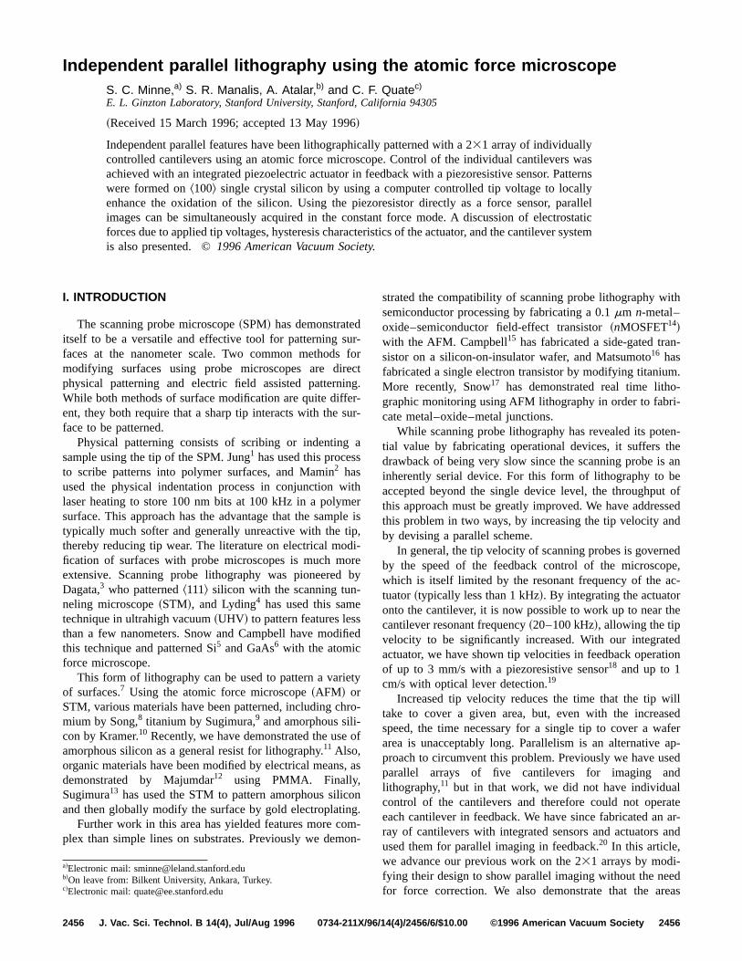
Figure 3~a! shows the output of a split photodetectowhen the ZnO voltage is swept from240 to 40 V and thenback to240 V. The inset of Fig. 3~a! shows an expandedview of the hysteresis loop around zero volts applied voltaThe maximum hysteresis of the ZnO in this voltage range20 nm. Unfortunately, it is not possible to determine the liearity of the actuator from Fig. 3~a!. The split photodiodedetector used to measure the position of the beam refleoff the cantilever has a limited range for which the outputlinear with respect to cantilever deflection. This limitatiooccurs because the size of the reflected beam is finitemust cover an adequate portion of both sides of the detecIn our microscope, the extent of the linear range cov
FIG. 3. ~a! Hysteresis curve for the ZnO actuator. The points representdata, while the solid line is a simulation of a Gaussian beam passing ovsplit photodiode. Inset: Expanded view of the data around zero appvoltage showing 20 nm maximum hysteresis.~b! Linearity plot for the ZnOactuator. The solid line is a composite curve of four photodiode positiorepresenting the overall linearity curve of the actuator. The points of theand final windows used to construct the overall plot are included. Tmethod was required because the cantilever displaced the beam beyonlinear range of the photodiode.
J. Vac. Sci. Technol. B, Vol. 14, No. 4, Jul/Aug 1996
eabyheultt of
r
ge.isn-
ctedisnandtor.ers
roughly 1mm of deflection and is insufficient to characterizethe entire range of the ZnO actuator. It is interesting to notethat the sigmoidal shape of Fig. 3~a! reflects the Gaussiandistribution of our laser diode. We have also simulated aGaussian beam traversing a split photodiode and plotted theresults with the data in Fig. 3~a!.
In order to measure linearity of the actuator, we manuallytranslated the linear window of the detector in discrete stepsso that it covered the entire range of the reflected laser beamThis provided us with a series of curves, each of which hasonly a small linear range. We then extracted and shifted thelinear data from each curve to construct the overall linearitycurve. The data was shifted such that overlapping voltages inadjacent windows had the same deflection.
Two such windows, which represent the initial and finaldata curves used for constructing the overall plot, along withthe final construction, are plotted in Fig. 3~b!. In these win-dows, the defector position was adjusted so that response islinear at the maximum excursion of the cantilever. Once thebeam is completely deflected to one side of the photodiode,the detector cannot provide information about the cantileverdeflection and the curves flatten. The composite curve of Fig.3~b! shows excellent linearity of the device over its entirerange of 3mm.
III. ELECTROSTATIC FORCES
Electrical AFM lithography involves applying a voltagebetween the tip and the substrate to be modified. The forceproduced by the applied voltage is the negative spatial de-rivative of the energy,U5 1
2CV2, whereC is the capacitance
andV is the voltage. The capacitance is primarily a functionof the distance between the tip and the sample, and the ef-fective area of the tip.
When the AFM operates in a repulsive mode~contact im-aging!, the electrostatic attraction produced by an appliedvoltage between the tip and sample increases the contacforce but does not cause the cantilever to deflect. If thesample is soft, the applied voltage provides a method forphysical modification using an electronic signal. If thesample is hard, the increased forces accelerate the wear othe delicate tip. Since the detector is sensitive only to canti-lever deflection, it is difficult to accurately monitor this at-tractive force while the tip remains in constant contact withthe surface.
In order to measure the contact force produced by theelectrostatic attraction, we retracted and extended the samplewhile monitoring the cantilever deflection with the piezore-sistor. A force curve was obtained by plotting the deflectionversus vertical position. Figure 4~a! shows a typical forcecurve where the sample is biased to27.5 V and being re-tracted from the tip. An additional bias is provided by thepiezoresistor measurement process. For this data, the extrabias is 0.6 V at the tip. The electrostatic attraction can bedetermined by multiplying the cantilever spring constant bythe distance for which the tip is electrostatically fixed to thesample during retraction. The electrostatic force is labeled‘‘ EF’’ on Fig. 4~a!. In our experiments, we find that the elec-
theer alied
nsfirsthisd the

c
-
2459 Minne et al. : Independent parallel lithography using AFM 2459
trostatic force is significantly greater than the meniscforce. The electrostatic force can be measured as a funcof applied voltage by reproducing the data in Fig. 4~a! formany voltages and is shown in Fig. 4~b!. A second orderpolynomial describes the data well in Fig. 4~b!, indicatingthat the force is proportional to the square of the applivoltage.
Figure 5~a! shows a scanning electron micrograph of thtip used to obtain the data in Fig. 4. This tip initially hadradius of curvature of;300 Å, but due to the process wused to measure the contact force versus voltage, thesharpness was reduced to;1.5 mm, as shown in Fig. 5~d!.During initial measurements made with this tip, we measua contact force of 20 nN for a voltage of 5 V. As the mesurement process was repeated, this force continued tocrease until stabilizing at a force of 1.25mN. Presumably thetip had dulled to a point that no further damage was occring. The results of Fig. 4 and 5 indicate that the contaforce between the tip and sample under an applied voltagdependent on the magnitude of the voltage and the degretip wear.
Preliminary results show that tip wear can be a significaproblem. In our lithographic experiments, we worked wisingle crystal silicon tips patterning single crystal silicosubstrates. Due to the hardness of the substrate andchemical interaction between silicon tip and silicon sampand because of the increased force due to the applied volt
FIG. 4. ~a! Force curve trace as the cantilever is retracted from the samThe sticking is due to the electrostatic attraction of the applied voltabetween the tip and sample.~b! The electrostatic attraction between the tiand the sample as a function of applied voltage.
JVST B - Microelectronics and Nanometer Structures
ustion
ed
eaetip
reda-in-
ur-cte ise of
ntthnthele,age,
the impact on the tip is substantial. Tips showing variousstates of wear are shown in Fig. 5. In Fig. 5~a!, we show anew tip which has a radius of curvature of;300 Å. Figure5~b! shows a tip that has performed and is still capable ofperforming high quality lithography, although the radius ofcurvature has increased to;2000 Å. Figure 5~c! shows a tipthat was originally effective in performing lithography buthas been worn down to the point where lithography is nolonger possible. The surface diameter of the tip is about 1mm. It can be seen that the tip wear is due to the scanningprocess and is exacerbated by the electrostatic forces fromthe voltage used for lithography—the straight angle on theworn tip corresponds to the scanning angle of our AFM. Webelieve that lithography fails as the tip wears because of thedecrease in electric field due to the dulling geometry of thetip and because most of the conductive implant in the tipregion has worn off.
IV. LITHOGRAPHY
Our preferred method for performing lithography is to usethe conductive path in the piezoresistor to apply appropriatevoltages to the conducting tip. Initially the ZnO was used tocontrol the lithography by biasing the sample and pulling thetip off the surface when lithography was not desired, but thismethod showed limited success due to the large electrostatiforces. In other attempts, we tried to use the ZnO as both thesensor and actuator,24 and dedicated the piezoresistor for
ple.gep
FIG. 5. SEM micrographs of~a! a new tip,~b! a slightly worn tip which isstill useful for silicon lithography,~c! a heavily worn tip which is no longeruseful for silicon lithography, and~d! the tip used for the measurement ofFig. 4. In ~d!, the heavy damage is due to the measurement process described in Fig. 4.
2460 Minne et al. : Independent parallel lithography using AFM 2460
lithographic voltages only. While this method provided gooimaging capabilities, the lithographic signal would often iterfere with the feedback loop. We believe that this approais still attractive, but at this time our cantilevers are not otimized for the use of the ZnO as a sensor.
In order to use the piezoresistor as both a sensor andelectrical conductor for lithography, it is necessary to seprate the two signals. By using an ac bridge, we can sepiezoresistor deflections at high frequency~typically 100kHz! while sending the electrical pulses for lithographthrough the cantilever at lower frequencies~filtered to 100Hz!. A benefit of this system is that very high scan speecan be obtained using the ac bridge~see Ref. 18!. Anotherconsideration when using the piezoresistor as a path forthography is electrical breakdown between the piezoresisand the bottom ZnO electrode. Referring back to Fig. 1,piezoresistor is separated from the bottom electrode by afilm of dielectric. Since the bottom electrode is heldground, a lithography signal can cause breakdown betwthe films. It is therefore necessary to bias both ZnO eltrodes and the piezoresistor with the lithography voltaused for writing the lithographic patterns.
Also, for high resolution imaging it is necessary to usehigh gain low noise amplifier for sensing the cantilever dflection. Unfortunately, the large voltage needed for lithogrphy normally precludes the use of such amplifiers in ocircuitry.
To address the problems of tip speed, dielectric bredown, and low noise amplification, two transformers andbattery powered amplifier were used in order to decouplecantilever from ground. By biasing the entire cantilever~bothZnO electrodes and the piezoresistor! to the lithography volt-age, the piezoresistor could be measured at ac without binfluenced by the high voltage lithographic signals. Also,biasing the entire cantilever, breakdown between the filmsno longer a concern. Duplicating the electronics for eachthe cantilevers within the array, parallel independent lithoraphy in feedback is readily accomplished.
In general, we have found that more reliable pattern geration is obtained by using a combination of open aclosed loop feedback. The open loop portion occurs owhen the lithography pulse is on. When writing, the Znexerts a force to partially oppose the electrostatic forcesorder to reduce tip wear and increase tip lifetime. In this wacantilevers are maintained in constant force mode as tprofile the surface. Only when writing voltage is applied dthey pull back from the surface to compensate for the eltrostatic force. Once the lithography signal is turned off, ttips return to the normal feedback mode. Lithography hbeen accomplished using both this mode as well as regclosed loop feedback.
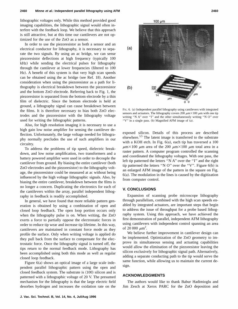
Figure 6~a! shows an optical image of a large scale indpendent parallel lithographic pattern using the open aclosed feedback system. The substrate is^100& silicon and ispatterned with a lithographic voltage of 20 V. The presummechanism for the lithography is that the large electric fiedesorbes hydrogen and increases the oxidation rate on
J. Vac. Sci. Technol. B, Vol. 14, No. 4, Jul/Aug 1996
dn-chp-
ana-nse
y
ds
li-torthethinateenec-ge
ae-a-ur
ak-athe
eingbyisofg-
en-ndnlyOiny,heyoec-heasular
e-nd
edldthe
exposed silicon. Details of this process are describedelsewhere.3,5 The latent image is transferred to the substratewith a KOH etch. In Fig. 6~a!, each tip has traversed a 100mm3100 mm area of the 200mm3100 mm total area in araster pattern. A computer program controlled the scanningand coordinated the lithography voltages. With one pass, theleft tip patterned the letters ‘‘N A’’ over the ‘‘I’’ and the righttip patterned the letters ‘‘N O’’ over the ‘‘V’’. Figure 6~b! isan enlarged AFM image of the pattern in the square on Fig.6~a!. The modulation in the lines is caused by the digitizationfrom computer control.
V. CONCLUSIONS
Expansion of scanning probe microscope lithographythrough parallelism, combined with the high scan speeds en-abled by integrated actuators, are important steps that beginto address the issue of throughput for a probe based lithog-raphy system. Using this approach, we have achieved thefirst demonstration of parallel, independent AFM lithographyusing cantilevers with independent control spanning an areaof 20 000mm2.
We believe further improvement in cantilever design canbe implemented. Optimization of the ZnO geometry to im-prove its simultaneous sensing and actuating capabilitieswould allow the elimination of the piezoresistor leaving thesilicon exclusively for lithographic signal path. Alternatively,adding a separate conducting path to the tip would serve thesame function, while allowing us to maintain the current de-sign.
ACKNOWLEDGMENTS
The authors would like to thank Babur Hadimioglu andJim Zesch at Xerox PARC for the ZnO deposition and
FIG. 6. ~a! Independent parallel lithography using cantilevers with integratedsensors and actuators. The lithography covers 200mm3100mm with one tipwriting ‘‘N A’’ over ‘‘I’’ and the other simultaneously writing ‘‘N O’’ over‘‘V’’ in a single pass.~b! Magnified AFM image of~a!.
2461 Minne et al. : Independent parallel lithography using AFM 2461
Charles Ahn and Nick Ulman for insightful discussions. Primary support for this work came from the Joint ServiceElectronics Program N0014-91-J-1050 of the Office of NavResearch with partial support from the NSF and CMR aStanford. S. C. M. acknowledges the support of the LelandEdwards Fellowship and S. R. M. acknowledges the suppoof the Urbanek Fellowship.
1T. A. Jung, A. Moser, H. J. Hug, D. Brodbeck, R. Hofer, H. R. Hidberand U. D. Schwarz, Ultramicroscopy42, 1446~1992!.2H. J. Mamin and D. Rugar, Appl. Phys. Lett.61, 1003~1992!.3J. A. Dagata, J. Schneir, H. H. Harary, C. J. Evans, M. T. Postek, andBennett, Appl. Phys. Lett.56, 2001~1990!.4J. W. Lyding, T. C. Chen, J. S. Hubacek, J. R. Tucker, and G. C. AbelAppl. Phys. Lett.64, 2010~1994!.5E. S. Snow and P. M. Campbell, Appl. Phys. Lett.64, 1932~1994!.6E. S. Snow, P. M. Campbell, and B. V. Shanabrook, Appl. Phys. Lett.63,3488 ~1993!.7C. R. K. Marrian,Technology of Proximal Probe Lithography~SPIE Op-tical Engineering, Bellingham, WA, 1993!.8H. J. Song, M. J. Rack, K. Abugharbieh, S. Y. Lee, V. Khan, D. K. Ferryand D. R. Allee, J. Vac. Sci. Technol. B12, 3720~1994!.9H. Sugimura, T. Uchida, N. Kitamura, and H. Masuhara, Appl. Phys. Le63, 1288~1993!.
10N. Kramer, H. Birk, J. Jorritsma, and C. Schonenberger, Appl. Phys. Le66, 1325~1995!.
JVST B - Microelectronics and Nanometer Structures
-saltT.rt
,
J.
n,
,
tt.
tt.
11S. C. Minne, Ph. Flueckiger, H. T. Soh, and C. F. Quate, J. Vac. Sci.Technol. B13, 1380~1995!.
12A. Majumdar, P. I. Oden, J. P. Carrejo, L. A. Nagahara, J. J. Graham, andJ. Alexander, Appl. Phys. Lett.61, 2293~1992!.
13H. Sugimura and N. Nakagiri, Jpn. J. Appl. Phys.34, 698 ~1995!.14S. C. Minne, H. T. Soh, Ph. Flueckiger, and C. F. Quate, Appl. Phys. Lett.6, 703 ~1995!.
15P. M. Campbell, E. S. Snow, and J. P. McMarr, Appl. Phys. Lett.66, 1388~1995!.
16K. Matsumoto, M. Ishii, K. Segawa, Y. Oka, B. J. Vartanian, and J. S.Harris, Extended Abstracts of 1994 International Conference of SolidState Device and Materials, Yokohama, Japan, 1994~unpublished!, p. 46.
17E. S. Snow and P. M. Campbell, Science270, 1639~1995!.18S. R. Manalis, S. C. Minne, and C. F. Quate, Appl. Phys. Lett.68, 871
~1996!.19S. R. Manalis, S. C. Minne, A. Atalar, and C. F. Quate, Rev. Sci. Instrum.
~to be published!.20S. C. Minne, S. R. Manalis, and C. F. Quate, Appl. Phys. Lett.67, 3918
~1995!.21M. Tortonese, Yamada, R. C. Barrett, and C. F. Quate,Proceedings ofTransducers ’91, IEEE Publ. No. 91 CH2817-5~IEEE, New York, 1991!,p. 448.
221020 cm23 under the ZnO, 531018 cm23 in the piezoresistor.23Y. Kanada, IEEE Trans. Electron. DevicesED-29, 64 ~1982!.24S. C. Minne, S. R. Manalis, A. Atalar, and C. F. Quate, Appl. Phys. Lett.68, 1427~1996!.
Related Documents


