arXiv:0906.0896v2 [cond-mat.mes-hall] 15 Sep 2009 Figure 1. a) bright field LEEM image (field of view: 15 μm, e - –energy: 2.68 eV) of the two graphene phases and uncovered Ir(111) at room temperature. b) Zoomed out PEEM image of the same area as in a) (field of view: 25 μm) The area used for the microdiffraction pattern in d) is illuminated by the electron beam (bright circle). c) microdiffraction pattern of the parallel graphene phase (electron energy: 45.9 eV) d) Zoomed out PEEM image of the same area as in a) (field of view: 25 μm) The bright spot marks the area used for the microdiffraction pattern in e) e) microdiffraction pattern of the rotated graphene phase (electron energy: 45.9 eV) In situ observation of stress relaxation in epitaxial graphene: Supplement I/II Alpha T. N’Diaye 1 ‡, Raoul van Gastel 2 , Antonio J. Mart´ ınez-Galera 3 , Johann Coraux 1 §, Hichem Hattab 4 , Dirk Wall 4 , Frank-J. Meyer zu Heringdorf 4 , Michael Horn–von Hoegen 4 , Jos´ eM.G´omez-Rodr´ ıguez 3 , Bene Poelsema 2 , Carsten Busse 1 , Thomas Michely 1 1. Parallel and rotated graphene phases in LEEM and PEEM We observe two domains of graphene on Ir(111). In 1 a) a bright field LEEM image is shown. Graphene in the upper area is imaged brighter than graphene in the lower ‡ Corresponding autor; Email: [email protected] § Permanent address: Institut N´ eel/CNRS-UJF, 25 rue des Martyrs, BP 166, 38042 Grenoble cedex 9, France

Welcome message from author
This document is posted to help you gain knowledge. Please leave a comment to let me know what you think about it! Share it to your friends and learn new things together.
Transcript

arX
iv:0
906.
0896
v2 [
cond
-mat
.mes
-hal
l] 1
5 Se
p 20
09
Figure 1. a) bright field LEEM image (field of view: 15µm, e−–energy: 2.68 eV) of
the two graphene phases and uncovered Ir(111) at room temperature. b) Zoomed out
PEEM image of the same area as in a) (field of view: 25µm) The area used for the
microdiffraction pattern in d) is illuminated by the electron beam (bright circle). c)
microdiffraction pattern of the parallel graphene phase (electron energy: 45.9 eV) d)
Zoomed out PEEM image of the same area as in a) (field of view: 25µm) The bright
spot marks the area used for the microdiffraction pattern in e) e) microdiffraction
pattern of the rotated graphene phase (electron energy: 45.9 eV)
In situ observation of stress relaxation in epitaxial
graphene: Supplement I/II
Alpha T. N’Diaye1‡, Raoul van Gastel2, Antonio J.
Martınez-Galera3, Johann Coraux1§, Hichem Hattab4, Dirk
Wall4, Frank-J. Meyer zu Heringdorf4, Michael Horn–von
Hoegen4, Jose M. Gomez-Rodrıguez3, Bene Poelsema2, Carsten
Busse1, Thomas Michely1
1. Parallel and rotated graphene phases in LEEM and PEEM
We observe two domains of graphene on Ir(111). In 1 a) a bright field LEEM image
is shown. Graphene in the upper area is imaged brighter than graphene in the lower
‡ Corresponding autor; Email: [email protected]§ Permanent address: Institut Neel/CNRS-UJF, 25 rue des Martyrs, BP 166, 38042 Grenoble cedex 9,
France

In situ observation of stress relaxation in epitaxial graphene: Supplement I/II 2
area, and there is a gulf of bare iridium cutting in from the right. The images b) and
e) are photo emission electron microscopy (PEEM) images of the same region. Iridium
is imaged black, graphene from the upper area of a) is imaged darker than graphene
from the lower area. The bright circle displays the position of the electron beam for
the LEED images in c) and e). The LEED patterns show that in the case of bright
graphene in LEEM (dark in PEEM), there is a rotation of graphene’s [1120] direction
with respect to the substrate’s [101] direction whereas in the dominating phase - darker
in LEEM (bright in PEEM) the dense packed directions of graphene and Ir(111) are
parallel.
2. Delamination around heptagon-pentagon pairs
Figure 2. STM topograph of graphene on Ir(111) (20 nm × 20nm). The moire rows
around the bulge are marked with bright lines.
The STM topograph in 2 shows a bulge in the graphene layer. The extra ending
line of moire maxima (three on one side of the protrusion, but four on the other) indicate
an extra row of atoms terminating in a pair of heptagon-pentagon carbon rings [1]. We
speculate that the bulge is a nucleus of a wrinkle originating from such a point defect.[1] J. Coraux, A. T. N’Diaye, C. Busse, and T. Michely. Structural coherency of graphene on Ir(111).
Nano Lett., 8:565–570, 2008.
arX
iv:0
906.
0896
v2 [
cond
-mat
.mes
-hal
l] 1
5 Se
p 20
09
In situ observation of stress relaxation in epitaxial
graphene
Alpha T. N’Diaye1‡, Raoul van Gastel2, Antonio J.
Martınez-Galera3, Johann Coraux1§, Hichem Hattab4, Dirk
Wall4, Frank-J. Meyer zu Heringdorf4, Michael Horn–von
Hoegen4, Jose M. Gomez-Rodrıguez3, Bene Poelsema2, Carsten
Busse1, Thomas Michely1
1 II. Physikalisches Institut, Universitat zu Koln, Zulpicher Straße 77, 50937 Koln,
Germany 2 MESA+ Institute for Nanotechnology, University of Twente, P.O.Box
217, 7500 AE Enschede, The Netherlands 3 Departamento de Fısica de la Materia
Condensada, C-III, Universidad Autonoma de Madrid, E-28049-Madrid, Spain 4
Institut fur Experimentelle Physik, Universitat Duisburg–Essen, Lotharstrasse 1,
47057 Duisburg, Germany
Abstract. Upon cooling, branched line defects develop in epitaxial graphene grown
at high temperature on Pt(111) and Ir(111). Using atomically resolved scanning
tunneling microscopy we demonstrate that these defects are wrinkles in the graphene
layer, i.e. stripes of partially delaminated graphene. With low energy electron
microscopy (LEEM) we investigate the wrinkling phenomenon in situ. Upon
temperature cycling we observe hysteresis in the appearance and disappearance of
the wrinkles. Simultaneously with wrinkle formation a change in bright field imaging
intensity of adjacent areas and a shift in the moire spot positions for micro diffraction
of such areas takes place. The stress relieved by wrinkle formation results from the
mismatch in thermal expansion coefficients of graphene and the substrate. A simple
one-dimensional model taking into account the energies related to strain, delamination
and bending of graphene is in qualitative agreement with our observations.
1. Introduction
The new material graphene receives currently an enormous attention for its exciting
properties. At the heart of the scientific interest are the consequences of graphene’s
unique band structure arising from its lattice symmetry and its monoatomic thickness
[1]. The high mobility of electrons in graphene and the strong electric field effect
foster work to realize graphene based electronics [2]. Moreover, the use of graphene
for conducting transparent electrodes [3, 4], to realize photosensitive transistors [5],
‡ Corresponding autor; Email: [email protected]§ Permanent address: Institut Neel/CNRS-UJF, 25 rue des Martyrs, BP 166, 38042 Grenoble cedex 9,
France
In situ observation of stress relaxation in epitaxial graphene 2
ultracapacitors [6], or a new class of catalytic and magnetic materials through templated
cluster growth has been suggested [7, 8].
Although the exciting electronic properties of graphene have been explored
mainly by transport measurements for devices built on flakes of exfoliated graphene
on SiO2, there appears to be consensus that for future scientific exploration and
technological applications epitaxial growth of high quality graphene over large areas
[9, 10, 11, 12, 13, 14, 15] is a prerequisite.
For any technological application it is of utmost importance to avoid or at least
control the defects in graphene associated with the epitaxial growth process. Such
defects may result from growth obstacles caused by substrate steps [10, 11] or by the
coalescence of finite sized graphene domains [13].
Branched line defects are present in mono- or multilayers of continuous graphene at
room temperature after high temperature (>1000K) epitaxial growth on several metals
and on SiC. Their nature has been under debate. While some authors attributed the
branched line defects to carbon nanotube formation [16, 17, 18, 19], current research
evidences that they are wrinkles in the graphene layers on SiC [20, 21, 22, 4] as
well as on metals [23, 24, 25]. For wrinkles in graphene on SiC very recent atomic
resolution scanning tunneling microscopy (STM) data provide unambiguous evidence
for the wrinkle interpretation [22]. Very recent LEEM and STM data provide evidence
for the presence of wrinkles also in monolayer graphene on Ir(111) [25]. Wrinkle features
have also been observed in layered transition metal dichalcogenides [26]. Among other
suggestions several authors attribute the occurrence of wrinkles to the difference in the
thermal expansion coefficients of graphene and its support [23, 20, 24, 22, 25]. Consistent
with that mismatch is the observation of compressive strain in epitaxial graphene at
room temperature [27, 28, 7]. This compression was found to vary on a length scale of
less then 300 nm [29]. Although in situ investigations could provide deeper insight into
the wrinkling phenomenon, such investigations are missing till now.
Here we not only support the wrinkle interpretation of the branched line defects
by atomically resolved scanning tunneling microscopy (STM) imaging of wrinkles on
metals, but also gain a detailed insight into wrinkle formation by in situ LEEM imaging
and micro diffraction. Most noteworthy, LEEM and micro diffraction ”see” not only
wrinkle formation but also the structural and electronic changes in adjacent µm-sized
areas within the graphene. A model is developed, which qualitatively agrees with our
observations.
2. Methods
We examined epitaxial graphene on Ir(111) and Pt(111). Graphene has been grown
epitaxially by chemical vapor deposition of ethene (C2H4) at elevated temperatures in
ultra high vacuum. Scanning tunneling microscopy (STM) was carried out at room
temperature, low energy electron microscopy (LEEM) imaging was done at variable
temperature. Growth and imaging was performed in ultra high vacuum without any
In situ observation of stress relaxation in epitaxial graphene 3
transfer outside the vacuum.
3. Results and discussion
3.1. Wrinkle formation
Figure 1 a) shows a bright field LEEM image of a graphene flake on Ir(111). The flake
has a diameter of ≈ 6 µm. Branched line defects on the flake which develop upon cooling
to room temperature form a network of dark lines, much darker than the substrate step
structure which can faintly be seen in the image as well [31]. The STM topograph
in figure 1 b) shows graphene islands on Pt(111). The branched line defects are also
present. A typical line defect is shown in figure 1 c). It crosses the image diagonally
and diverges in two at the bottom of the image. It roughly follows the direction of the
two monoatomic steps of the underlying Ir(111) substrate. The defect is about 3 nm
high, and thus much higher than a substrate step as shown in figure 1 e). Its width is
a few nanometers as well. On low line defects as shown in figure 1 d), profile in figure
1 f), it is possible to achieve atomic resolution on the ridge. The atomic rows over the
defect are continuous. The dense packed rows cross the wrinkle roughly perpendicular.
The fact that these structures are present only on the graphene flakes and never on the
uncovered part of the surface corroborates the assumption that they are indeed wrinkles
and not nanotubes on the sample, as has been proposed previously [16, 17, 18, 19]. The
continuity of the atomic rows also indicates that the elongated structures are not formed
at ruptures where the islands edges roll or bend up.
The LEEM images in figure 2 a) show epitaxial graphene on Ir(111) fully covering
the field of view. As visible in micro diffraction (see supplement) the darker graphene
domain on the left is rotated with respect to the substrate [25]. The left image [figure
2 a) I] has been taken at high temperature (1100K), close to the growth temperature
(Tgrow=1320K) of graphene. No wrinkles are observed. During cooling wrinkles appear
and spread all over the field of view as visible in figure 2 a) II. Upon reannealing close to
the growth temperature, the wrinkles disappear again [figure 2 a) III]. Faint dark lines
due to steps are present at all temperatures. The time and temperatures the images
have been recorded at are marked with green dots in the temperature vs. time diagram
in figure 2 b).
The appearance of a wrinkle is an instant process within the time resolution of our
measurement of 1 s, while the decay of the wrinkles is a gradual process. Wrinkles decay
at slightly higher temperatures than they form. The red squares in figure 2 b) indicate
the formation and decay temperatures. This also reflects in a hysteresis of the average
lattice parameter of graphene as measured by spot profile analysis LEED measurements
[32].
Graphene has been grown at several temperatures and the onset temperature of
wrinkle formation has been recorded. The onset of wrinkle formation is measured as
the occurrence of the first wrinkle in a field of view of 10µm. Soon after the occurrence of

In situ observation of stress relaxation in epitaxial graphene 4
Figure 1. a) LEEM image (field of view: 10µm, electron energy: 2.8 eV) of a
graphene flake on Ir(111) at room temperature. b) STM topograph of graphene flakes
on Pt(111) (3 µm × 3 µm). The image is differentiated and appears as if illuminated
from the left. The inset shows the same image, with the graphene flakes highlighted in
red. c) STM topograph (240 nm × 240nm) of a full layer of graphene on Ir(111) with
a wrinkle. The bright line corresponds to the profile given in e). d) STM topograph
(7 nm × 7 nm) of a wrinkle of low height in graphene on Pt(111) in atomic resolution.
The bright line corresponds to the profile given in f). e) Profile of the topography of
the wrinkle in graphene on Ir(111) shown in c). f) Profile of the topography of the
wrinkle in graphene on Pt(111) shown in d). STM images have been processed using
the WSxM software [30].

In situ observation of stress relaxation in epitaxial graphene 5
Figure 2. a) Three bright field LEEM images (field of view: 10µm, electron energy:
2.7 eV) of Ir(111) fully covered with two differently oriented domains of epitaxial
graphene. Images I and III have been taken at 1110K while II has been imaged
at 410K. b) Temperature evolution measured at the sample with a pyrometer (black
curve), and at the sample holder with a thermocouple (grey curve). The green dots
mark the points where a) I-III were recorded. The red squares mark the onset of wrinkle
formation upon cooling and the disappearance of the last wrinkle upon heating. c)
The difference ∆T of the onset of wrinkle formation Tw and the graphene growth
temperature Tgrow based on the pyrometer measurement is plotted as a function of
Tgrow.
the first wrinkle additional wrinkles emerge and continue to form even until the sample is
cooled down to room temperature. The first wrinkles appear after a cooldown of 410K
± 40K regardless of the growth temperature [see figure 2 c)]. Assuming an average
difference of the thermal expansion coefficients of Ir and graphene of 7.15 × 10⁻⁶ a
temperature difference translates to a mismatch in expansion. During a cooldown by
410K iridium shrinks by 0.33% while a graphene layer only shrinks by 0.03% [33, 34].
The remaining 0.3% have to be taken up by compression or wrinkling of the graphene.
This suggests a stress driven process for wrinkle formation.
In situ observation of stress relaxation in epitaxial graphene 6
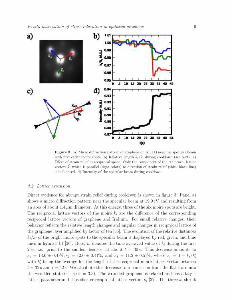
Figure 3. a) Micro diffraction pattern of graphene on Ir(111) near the specular beam
with first order moire spots. b) Relative length ki/ki during cooldown (see text). c)
Effect of strain relief in reciprocal space. Only the component of the reciprocal lattice
vectors ~ki which is parallel (light colors) to direction of strain relief (thick black line)
is influenced. d) Intensity of the specular beam during cooldown.
3.2. Lattice expansion
Direct evidence for abrupt strain relief during cooldown is shown in figure 3. Panel a)
shows a micro diffraction pattern near the specular beam at 19.9 eV and resulting from
an area of about 1.4µm diameter. At this energy, three of the six moire spots are bright.
The reciprocal lattice vectors of the moire ki are the difference of the corresponding
reciprocal lattice vectors of graphene and Iridium. For small relative changes, their
behavior reflects the relative length changes and angular changes in reciprocal lattice of
the graphene layer amplified by factor of ten [35]. The evolution of the relative distances
ki/ki of the bright moire spots to the specular beam is displayed by red, green, and blue
lines in figure 3 b) [36]. Here, ki denotes the time averaged value of ki during the first
25 s, i.e. prior to the sudden decrease at about t = 30 s. This decrease amounts to
s1 = (3.6 ± 0.4)%, s2 = (2.0 ± 0.4)%, and s3 = (1.2 ± 0.5)%, where si = 1 − ki/k′i
with k′i being the average for the length of the reciprocal moire lattice vector between
t = 32 s and t = 42 s. We attribute this decrease to a transition from the flat state into
the wrinkled state (see section 3.3). The wrinkled graphene is relaxed and has a larger
lattice parameter and thus shorter reciprocal lattice vectors ~ki [37]. The three ~ki shrink

In situ observation of stress relaxation in epitaxial graphene 7
by different amounts. This is well understandable given the wrinkle is a linear defect
which can only relax stress in one direction. Assuming all three ~ki to be of equal length
and making angles of exactly 120◦ prior to wrinkling, we can estimate the direction
of stress relaxation. Each vector ~ki can be split into a component which is parallel
to the direction of strain relief and one which is perpendicular to this direction. Only
the parallel component is affected by the strain relief. Let φi be the angle between
the lattice vector ~ki and the direction of strain relief, ki and k′i the averaged lengths of
the reciprocal lattice vectors before and after the transition, ki,‖ = ki cos φi the average
component parallel and ki,⊥ = ki sin φi the average component of ~ki perpendicular to
the direction of strain relaxation and prior to the relaxation and finally c = k′i,‖/ki,‖ the
reciprocal space compression upon wrinkling. This leads to
1 −
(
k′i
ki
)2
= (1 − c2) cos2 φi
for all three reciprocal linearly dependent lattice vectors. With the measured values fork′
i
ki
this equation can be numerically solved. This leads to a factor c = 96% corresponding
to a strain relief of 0.4% in the graphene layer. The angle between the direction of
compression and ~k1 is roughly φ1 = 10◦ as illustrated in figure 3 c). This implies that
the wrinkling took place roughly perpendicular to the dense packed rows of the graphene
layer consistent with what is expected from STM data as the dominant orientation of
wrinkles (cf. figure 1 d) or [22]) The intensity of the specular beam abruptly increases
simultaneously with the relaxation of the lattice as shown in figure 3 d).
3.3. Local stress evolution
The abrupt intensity change of the specular beem upon wrinkling allows us to monitor
the local extension of stress relaxation through LEEM imaging. Figure 4 a) shows LEEM
images of graphene on Ir(111). The sample is partially covered by graphene prepared at
1110K and the sample has been cooled down to 560K within one hour. In the course of
this cooling, some wrinkles have already formed, especially in the right hand side of the
field of view. The images I and II have been measured subsequently with a delay of 1 s.
They capture a single event of wrinkle formation on the graphene patch near the left
border of the image. Simultaneously with wrinkle formation the brightness increases
in the affected area. This change is visualized in figure 4 a) III which is the difference
between the images in II and I. It shows that the formation of a wrinkle does not only act
nanoscopically at the line of delamination but it rather has an impact on a mesoscopic
scale (in this case 4µm2).
The change in intensity integrated over the regions marked in figure 4 a) I is shown
in figure 4 b). This change takes place at different times, locations and to different
extents. We interpret the increase in image intensity as an effect of the relaxation of
the graphene lattice. This provides an explanation for the observation of locally varying
compression in epitaxial graphene [29].

In situ observation of stress relaxation in epitaxial graphene 8
Figure 4. a) Two subsequent LEEM images of graphene on Ir(111) recorded during
cooling (field of view: 10µm, electron energy: 2.5 eV) and the difference of their
intensities with enhanced contrast. Between (I) and (II) a wrinkle forms on the
peninsula on the left. This is shown enlarged and contrast enhanced in the insets.
The difference image shows that the intensity has increased locally in the course of
wrinkle formation. b) The intensity integrated over the regions marked by colored
boxes in a) I over time, with linear background subtraction. Whenever a wrinkle is
created, the brightness increases abruptly. The roman numbering indicates where a) I
and a) II have been recorded. c) LEEM I(V)-curve. Blue: unwrinkled graphene, red:
wrinkled graphene, purple: difference (×20).
To discuss the origin of the (0, 0)-spot intensity increase upon wrinkling we consider
figure 4 c). It shows I(V)-curves of the (0, 0) spot of flat and wrinkled graphene on Ir(111)
and their difference. The curves were taken from one sequence of images recorded at
intermediate temperatures where wrinkles have just started to form and some parts
of the surface are still unwrinkled. The difference curve has two maxima. Both are
correlated with maxima in total intensity resulting from constructive interference of
electron waves reflected from graphene and the Ir surface. For a distance of 3.4 A [38]
we expect maxima at 3.2 eV and 13 eV. Therefore we speculate that the intensity changes

In situ observation of stress relaxation in epitaxial graphene 9
are due to structural changes, such as a change in the spacing between the graphene layer
and the Ir substrate triggered by the relaxation of the graphene lattice. Evidently these
structural relaxations are accompanied by changes in the graphene electronic structure
which additionally may affect the I(V)-curve.
During a wrinkling event many atoms are displaced. On Ir(111) and Pt(111)
graphene forms an incommensurate superstructure [35, 39]. That implies a low barrier
for sliding of graphene on the surface, because for every atom, which loses energy by
moving out of its optimum binding configuration another atom gains energy. The small
flakes grown by temperature programmed growth [13] barely show wrinkles. A graphene
flake smaller than the average separation of two wrinkles just expands if the compression
gets large enough to overcome the barrier for sliding. For smaller islands, this barrier
may be larger, due to edge effects becoming more relevant. Accordingly there is residual
strain in such flakes [35].
Wrinkle patterns from repeated cooling and heating cycles at one sample spot are
similar. This suggests that wrinkles nucleate at preexisting features. We find in our STM
data spots of delamination which are centered at heptagon-pentagon pairs of carbon
rings (see supplement) [40]. This seems reasonable as these defects induce additional
local stress into the graphene lattice. We thus speculate that heptagon-pentagon defects
are sites of wrinkle nucleation.
3.4. Model
The wrinkle formation can be described in a one-dimensional continuum model. When
the substrate and graphene cool down, the graphene has to compensate for the thermal
misfit ∆L/L resulting from the difference of the thermal expansion coefficients. Either
compression ∆Lc/L or the formation of a wrinkle ∆Lw/L can compensate for that misfit
(∆L = ∆Lc + ∆Lw).
To calculate the energy of compression we use the separation between two
wrinkles L = 260 nm as estimated from experiment. With an atom density of
n = 36.2 atoms/nm2 and an elastic modulus of Y = 56 eV per atom [41] the compression
energy per nm of wrinkle length can be expressed as Ec = 12(∆Lc/L)2L · Y · n. The
energy necessary for wrinkle formation consists of two contributions: first, there is the
bending of the graphene layer. An estimation for this contribution is available from the
study of single walled carbon nanotubes [41], giving the bending energy per atom in a
nanotube of radius r as ew = a/r2 + b/r4 with the empirical parameters a = 0.99 eV/A2
and b = 12.3 eV/A4. Second, bonds between graphene and the substrate are stretched
or broken, where the graphene flake delaminates. Since the estimated height of graphene
on Ir(111) is comparable to the interlayer distance of graphite, we use the exfoliation
energy of graphite as an assessment for the binding energy of an atom in a graphene
layer on Ir(111) in this case. It has the value of eb,0 = 0.052eV [42, 43] The strength
of the van-der-Waals binding energy between a particle and a surface decreases with
the cube of the distance, so we calculate the change in binding energy of an atom in an

In situ observation of stress relaxation in epitaxial graphene 10
Figure 5. a) A map of the energy per nm of a wrinkle Etot with respect to
uncompressed flat graphene according to a one-dimensional continuum model. The
shape of the wrinkle has been modeled as four arcs of circles (see inset). The lower
horizontal axis shows the misfit of graphene and Ir ∆LL
, the upper axis shows the
corresponding temperature difference ∆T . The vertical axis represents the fraction of
the misfit which is compensated by wrinkling ∆Lw
∆Linstead of compression. b) The
graph shows the energy of a wrinkle per nm for a mismatch of 0.7% (thick black line)
and the contributions it consists of. There is a local minimum for the flat configuration
where all the energy is stored in the form of compression Ec, while in the global energy
minimum most of the energy is stored in a wrinkle as bending and reduced bonding.
c) Energy barrier EB,w for wrinkle formation. The system can gain energy by wrinkle
formation (Egain) with respect to compressed flat graphene, if the misfit is larger than
0.65%.

In situ observation of stress relaxation in epitaxial graphene 11
elevated part of the graphene sheet with the height of z instead of z0 above the substrate
as eb = eb,0 (1 − z30/z
3).
With Ew and Eb as the integral of ew and eb over the atoms in a nm of wrinkle the
resulting energy cost for a nm of wrinkle compared to flat relaxed graphene sums up to
Etot = Ec + Ew + Eb
=1
2(∆Lc/L)2 · Y · L · n
+ n∫ L−∆Lc
0
(
a
r(x)2+
b
r(x)4
)
dx
+ n∫ L−∆Lc
0
(
eb,0
(
1 −z30
z3
))
dx
and leads to a complex variation problem for the shape of the wrinkle.
Here we assume a simple shape for the wrinkle, consisting of four equal arcs of a
circle with radius r and an opening angle α as shown in the inset of figure 5 a). The
model contains r (or α) as a free parameter which is optimized for minimum energy Etot
for each combination of ∆L/L and ∆Lw/L.
In figure 5 a) Etot is plotted for this model as a function of thermal misfit ∆L/L
(lower horizontal axis) and fraction of strain accommodated in a wrinkle ∆Lw/∆L
(vertical axis). Moving along the horizontal axis from left to right corresponds to cooling
of the sample. The according temperature difference is indicated on the upper horizontal
axis. In the lower part of the diagram most of the misfit is taken up by compression
while in the upper part the misfit is compensated for by a wrinkle. For misfits below
0.3% there is exactly one optimum configuration: The graphene layer is compressed
and there is no wrinkle. As the misfit increases (temperature decreases), a second local
minimum in energy emerges. Nevertheless, the unwrinkled compressed state still is
favorable. For ∆L/L > 0.65% of misfit, a situation rendering about 80% of the misfit
subject to wrinkle formation, is optimal.
A cut through the map at constant misfit ∆L/L = 0.7% is shown in figure 5 b).
There is a local minimum for the flat configuration where all the energy is stored in the
form of compression Ec, but the optimum configuration is the formation of a wrinkle,
which contains most of the energy in the form of reduced bonding to the substrate (Eb)
and bending of the graphene (Ew). Figure 5 c) illustrates the relationship of the two
energy minima and the barrier in between. The gray line shows the difference in energy
of the unwrinkled state and the wrinkled state Egain. For a misfit below 0.47% there is no
minimum for the wrinkled state, above 0.47%, there is a local minimum, but its energy
is higher than that of the uncompressed flat state. Only for compressions above 0.65%,
when the gray line enters the negative region, the system can gain energy by forming
a wrinkle. Still, there is an energy barrier to overcome, which allows the system to be
trapped in the local minimum explaining the sudden and abrupt formation of wrinkles.
This is consistent with the hysteresis for wrinkle appearance and disappearance.
Although our one-dimensional model explains all qualitative features observed, the
model prediction overestimates the experimentally observed critical misfit for wrinkling
In situ observation of stress relaxation in epitaxial graphene 12
formation nearly by a factor of two. Certainly a full two dimensional analysis may lead
to somewhat different numbers – wrinkle formation is likely to be eased by biaxially
compressed graphene. Also the wrinkle separation L, the binding energy Eb,0 and our
simple model for the wrinkle shape carry significant uncertainties.
As wrinkles are large scale defects, it would be desirable to suppress their formation.
One way to achieve this could be to reduce the amount of total thermal misfit by growing
graphene at the lowest possible temperature and inserting an intermediate annealing
step to remove the defects prior to cooldown. Combining temperature programmed
growth and chemical vapor deposition it appears possible to achieve high quality
graphene at a growth temperature of only 1000K [44]. Also grazing incidence keV
ion erosion removing exclusively protruding wrinkles followed by annealing could lead
to continuous graphene with less or no wrinkles. A third approach could be to increase
the energy for bending. This could be accomplished by evaporating at high substrate
temperatures a thin film with a thermal expansion coefficient similar to the substrate
on top of the graphene. This cover layer would have to be bent as well, for the graphene
to form a wrinkle.
4. Conclusion
In conclusion, we demonstrated how LEEM can be used to monitor strain relaxation in
situ. It was possible to develop a consistent picture of wrinkle formation on graphene
linking wrinkle formation with inhomogeneous residual strain. The development
of wrinkles appears to be a serious problem for all methods of growth of weakly
bound epitaxial graphene, as all require high temperatures. We hope the improved
understanding of wrinkle formation achieved here will contribute to a future solution of
this problem.
5. Acknowledgement
Financial support by Spain’s MEC under grant No. MAT2007-60686 and Deutsche
Forschungsgemeinschaft is gratefully acknowledged. J. C. was supported by a Humboldt
fellowship.
6. Supporting information
S1: LEEM, photo electron emission microscopy and microdiffraction measurements of
rotational domains, STM data of a delaminated bulge around a dislocation. S2: Movie
with brightness increase upon wrinkle formation as in figure 4.[1] P. R. Wallace. The band theory of graphite. Phys. Rev., 71:622, 1947.
[2] A. H. Castro Neto, F. Guinea, N. M. R. Peres, K. S. Novoselov, and A. K. Geim. The electronic
properties of graphene. Rev. Mod. Phys., 81:109–162, 2009.

In situ observation of stress relaxation in epitaxial graphene 13
[3] A. Reina, X. Jia, J. Ho, D. Nezich, H. Son, V. Bulovic, M. S. Dresselhaus, and J. Kong. Large
area, few-layer graphene films on arbitrary substrates by chemical vapor deposition. Nano Lett.,
9 (1):30–35, 2009.
[4] K. S. Kim, Y. Zhao, H. Jang, S. Y. Lee, J. M. Kim, K. S. Kim, J.-H. Ahn, P. Kim, J.-Y. Choi, and
B. H. Hong. Large-scale pattern growth of graphene films for stretchable transparent electrodes.
Nature, 457:706–710, 2009.
[5] F. Xia, T. Mueller, R. Golizadeh-Mojarad, M. Freitag, Yu-Ming Lin, J. Tsang, V. Perebeinos,
and P. Avouris. Photocurrent imaging and efficient photon detection in a graphene transistor.
Nano Lett., 9:1039–1044, 2009.
[6] M. D. Stoller, S. Park, Y. Zhu, J. An, and R. S. Ruoff. Graphene-based ultracapacitors. Nano
Lett., 8:3498–3502, 2008.
[7] A. T. N’Diaye, S. Bleikamp, P. J. Feibelman, and T. Michely. Two-dimensional Ir cluster lattices
on a graphene moire on Ir(111). Phys. Rev. Lett., 97:215501, 2006.
[8] A. T. N’Diaye, T. Gerber, C Busse, J. Coraux J. Myslivecek, and T. Michely. A versatile fabrication
method for cluster superlattices. ArXiv:0908.3800, 2009. submitted to New J. Phys.
[9] R. Tromp and J. B. Hannon. Thermodynamics and kinetics of graphene growth on SiC(0001).
Phys. Rev. Lett., 102:106104, 2009.
[10] K. V. Emtsev, A. Bostwick, K. Horn, J. Jobst, G. L. Kellogg, L. Ley, J. L. McChesney, T. Ohta,
S. A. Reshanov, J. Rohrl, E. Rotenberg, A. K. Schmid, D. Waldmann, H. B. Weber, and
T. Seyller. Towards wafer-size graphene layers by atmospheric pressure graphitization of silicon
carbide. Nat. Mat., 8:203–207, 2009.
[11] P. W. Sutter, J.-I. Flege, and E. A. Sutter. Epitaxial graphene on ruthenium. Nat. Mat., 7:406
– 411, 2008.
[12] E. Loginova, N. C. Bartelt, P. J. Feibelman, and Kevin F. McCarty. Evidence for graphene growth
by C cluster attachment. New J. Phys., 10:093026, 2008.
[13] J. Coraux, A. T. N’Diaye, M. Engler, C. Busse, D. Wall, N. Buckanie, F.-J. Meyer zu Heringdorf,
R. van Gastel, B. Poelsema, and T. Michely. Growth of graphene on Ir(111). New J. Phys.,
11:023006, 2009.
[14] Q. Yu, J. Lian, S. Siriponglert, H. Li, Y. P. Chen, and S. Pei. Graphene segregated on ni surfaces
and transferred to insulators. Appl. Phys. Lett., 93:113103, 2008.
[15] S. Marchini, S. Gunther, and J. Wintterlin. Scanning tunneling microscopy of graphene on
Ru(0001). Phys. Rev. B, 76:075429, 2007.
[16] V. Derycke, R. Martel, M. Radosavljevic, F. M. Ross, and Ph. Avouris. Catalyst-free growth of
ordered single-walled carbon nanotube networks. Nano Lett., 2:1043–1046, 2002.
[17] D. E. Starr, E. M. Pazhetnov, A. I. Stadnichenko, A. I. Boronin, and S. K. Shaikhutdinov. Carbon
films grown on Pt(111) as supports for model gold catalysts. Surf. Sci., 600:2688–2695, 2006.
[18] D. Fujita, T. Kumakura, K. Onishi, K. Sagisaka, T. Ohgi, and M. Harada. Sprout-like growth of
carbon nanowires on a carbon-doped Ni(111) surface. Surf. Sci., 566-581:361–366, 2006.
[19] I. A. Nyapshaev, I. V. Makarenko, A. N. Titkov, A. V. Tyurnina, and A. N. Obraztsov. Structural
peculiarities of carbon nanolayers prepared by deposition from a gaseous phase on Ni. Phys. of
the Solid State, 51:1054–1059, 2009.
[20] Z. G. Cambaz, G. Yushin, S. Osswald, V. Mochalin, and Y. Gogotsi. Noncatalytic synthesis of
carbon nanotubes, graphene and graphite on SiC. Carbon, 46:841–849, 2008.
[21] L. B. Biedermann, M. L. Bolen, M. A. Capano, D. Zemlyanov, and R. G. Reifenberger. Insights
into few-layer epitaxial graphene growth on 4H-SiC(0001) substrates from STM studies. Phys.
Rev. B, 79:125411, 2009.
[22] G. F. Sun, J. F. Jia, Q. K. Xue, and L. Li. Atomic-scale imaging and manipulation of ridges on
epitaxial graphene on 6H-SiC(0001). Nanotechnology, 20:355701, 2009.
[23] A. N. Obraztsov, E. A. Obraztsova, A. V. Tyurnina, and A. A. Zolotukhin. Chemical vapor
deposition of thin graphite films of nanometer thickness. Carbon, 45:2017–2021, 2007.
[24] S. J. Chae, F. Gnes, K. K. Kim, E. S. Kim, G. H. Han, S. M. Kim, H.-J. Shin, S.-M. Yoon, J.-Y.

In situ observation of stress relaxation in epitaxial graphene 14
Choi, M. H. Park, C. W. Yang, D. Pribat, and Y. H. Lee. Synthesis of large-area graphene
layers on poly-nickel substrate by chemical vapor deposition: Wrinkle formation. Advanced
Mat., 21:2328–2333, 2009.
[25] E. Loginova, S. Nie, K. Thurmer, N. C. Bartelt, and K. F. McCarty. Defects of graphene on
Ir(111): rotational domains and ridges. arXiv:0904.1251, 2009.
[26] E. Spiecker, A. K. Schmid, A. M. Minor, U. Dahmen, S. Hollensteiner, and W. Jager. Self-
assembled nanofold network formation on layered crystal surfaces during metal intercalation.
Phys. Rev. Lett., 96:086401, 2006.
[27] J. Hass, F. Varchon, J. E. Millan-Otoya, M. Sprinkle, N. Sharma, W. A. de Heer, C. Berger, P. N.
First, L. Magaud, and E. H. Conrad. Why multilayer graphene on 4H-SiC(0001) behaves like a
single sheet of graphene. Phys. Rev. Lett., 100:125504, 2008.
[28] N. Ferralis, R. Maboudian, and C. Carraro. Evidence of structural strain in epitaxial graphene
layers on 6H-SiC(0001). Phys. Rev. Lett., 101:156801, 2008.
[29] J. A. Robinson, C. P. Puls, N. E. Staley, J. P. Stitt, M. A. Fanton, K. V. Emtsev, Th. Seyller,
and Ying Liu. Raman topography and strain uniformity of large-area epitaxial graphene. Nano
Lett., 9:964–968, 2009.
[30] I. Horcas, R. Fernandez, J. M. Gomez-Rodrıguez, J. Colchero, J. Gomez-Herrero, and A. M. Baro.
WSXM: A software for scanning probe microscopy and a tool for nanotechnology. Rev. Sci.
Instrum., 78:013705, 2007.
[31] The rim of the flake appears very broad and dark, because the electric field at the edge of the
island deteriorates the imaging electron beam.
[32] to be published.
[33] R. T. Wimber. High-temperature thermal expansion of iridium (revised results). J. Appl. Phys.,
47:5115, 1976.
[34] Dwight E. Gray, editor. American Institute of Physics Handbook 2nd Ed., volume 4. McGraw–Hill
Book Company, 1963.
[35] A. T. N’Diaye, J. Coraux, T. N. Plasa, C. Busse, and T. Michely. Structure of epitaxial graphene
on Ir(111). New J. Phys., 10:043033, 2008.
[36] The distances of the moire spots from the (0,0) spot are determined by the differences of the
reciprocal lattice vectors of graphene and Ir(111) and amount to about 20 pixels in the original
data. To determine these distances with sub pixel resolution, a two dimensional gauss peak has
been fitted into each LEED-spot. The centers of the gauss peaks accurately point to the center
of the spots.
[37] Slightly rotated domains can also lead to changes in the moire repeat distance. This is excluded
here.
[38] P. J. Feibelman. Pinning of graphene to Ir(111) by flat Ir dots. Phys. Rev. B, 77:165419, 2008.
[39] T. A. Land, T. Michely, R. J. Behm, J. C. Hemminger, and G. Comsa. STM investigation of
single layer graphite structures produced on Pt(111) by hydrocarbon decomposition. Surf. Sci.,
264:261–270, 1992.
[40] J. Coraux, A. T. N’Diaye, C. Busse, and T. Michely. Structural coherency of graphene on Ir(111).
Nano Lett., 8:565–570, 2008.
[41] J.-W. Jiang, H. Tang, B.-S. Wang, and Z.-B. Su. A lattice dynamical treatment for the total
potential energy of single-walled carbon nanotubes and its applications: relaxed equilibrium
structure, elastic properties, and vibrational modes of ultra-narrow tubes. J. Phys.: Condens.
Matter, 20:045228, 2008.
[42] R. Zacharia, H. Ulbricht, and T. Hertel. Interlayer cohesive energy of graphite from thermal
desorption of polyaromatic hydrocarbons. Phys. Rev. B., 69:155406, 2004.
[43] Although the bond strength between graphene and Ir(111) has been calculated with density
functional theory (DFT) to be marginal [35, 38], due to Van-der-Waals interactions which are
not covered by DFT, the actual bond will be stronger than calculated.
[44] R. van Gastel, A. T. N’Diaye, D. Wall, J. Coraux, C. Busse, N. Buckanie, F.-J. Meyer zu

In situ observation of stress relaxation in epitaxial graphene 15
Heringdorf, M. Horn von Hoegen, T. Michely, and B. Poelsema. Selecting a single orientation
for millimeter sized graphene sheets. Appl. Phys. Lett., in print, 95, 2009.
Related Documents


