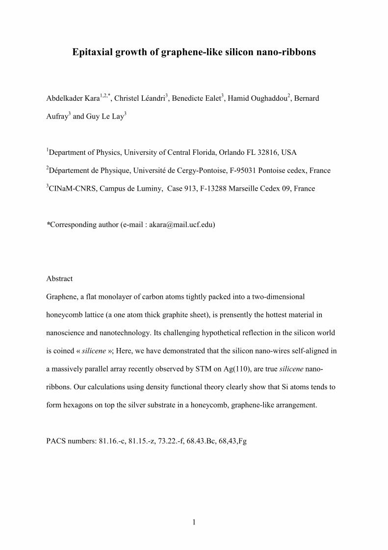
1 Epitaxial growth of graphene-like silicon nano-ribbons Abdelkader Kara 1,2,* , Christel Léandri 3 , Benedicte Ealet 3 , Hamid Oughaddou 2 , Bernard Aufray 3 and Guy Le Lay 3 1 Department of Physics, University of Central Florida, Orlando FL 32816, USA 2 Département de Physique, Université de Cergy-Pontoise, F-95031 Pontoise cedex, France 3 CINaM-CNRS, Campus de Luminy, Case 913, F-13288 Marseille Cedex 09, France *Corresponding author (e-mail : [email protected]) Abstract Graphene, a flat monolayer of carbon atoms tightly packed into a two-dimensional honeycomb lattice (a one atom thick graphite sheet), is prensently the hottest material in nanoscience and nanotechnology. Its challenging hypothetical reflection in the silicon world is coined « silicene »; Here, we have demonstrated that the silicon nano-wires self-aligned in a massively parallel array recently observed by STM on Ag(110), are true silicene nano- ribbons. Our calculations using density functional theory clearly show that Si atoms tends to form hexagons on top the silver substrate in a honeycomb, graphene-like arrangement. PACS numbers: 81.16.-c, 81.15.-z, 73.22.-f, 68.43.Bc, 68,43,Fg

Welcome message from author
This document is posted to help you gain knowledge. Please leave a comment to let me know what you think about it! Share it to your friends and learn new things together.
Transcript
1
Epitaxial growth of graphene-like silicon nano-ribbons
Abdelkader Kara1,2,*, Christel Léandri3, Benedicte Ealet3, Hamid Oughaddou2, Bernard
Aufray3 and Guy Le Lay3
1Department of Physics, University of Central Florida, Orlando FL 32816, USA
2Département de Physique, Université de Cergy-Pontoise, F-95031 Pontoise cedex, France
3CINaM-CNRS, Campus de Luminy, Case 913, F-13288 Marseille Cedex 09, France
*Corresponding author (e-mail : [email protected])
Abstract
Graphene, a flat monolayer of carbon atoms tightly packed into a two-dimensional
honeycomb lattice (a one atom thick graphite sheet), is prensently the hottest material in
nanoscience and nanotechnology. Its challenging hypothetical reflection in the silicon world
is coined « silicene »; Here, we have demonstrated that the silicon nano-wires self-aligned in
a massively parallel array recently observed by STM on Ag(110), are true silicene nano-
ribbons. Our calculations using density functional theory clearly show that Si atoms tends to
form hexagons on top the silver substrate in a honeycomb, graphene-like arrangement.
PACS numbers: 81.16.-c, 81.15.-z, 73.22.-f, 68.43.Bc, 68,43,Fg
2
Pure carbon crystals exist on earth in the form of either cubic diamond gems or simple
hexagonal graphite. Graphene, the two-dimensional (2D) one-atom thick single layer building
sheet of graphite, is the hottest new material in physics and nanotechnology. It has striking
exotic properties, which open potentially novel routes for many applications [1-3]. However,
despite the reigning optimism about graphene-based electronics, its discoverers underline that
« graphenium » microprocessors are unlikely to appear for the next 20 years [4]. An obvious
reason is that replacement of silicon electronics is a tough hurdle. Indeed, silicon-based
nanotechnology is highly promising since it is compatible with conventional silicon
microtechnology; hence, there has been recently considerable interest in the fabrication,
characterization and properties of silicon nanowires (silicon NWs) and nanodots (silicon NDs
[5]). Silicene [6], the counterpart of graphene in the silicon nano-world has not been found
until now, although it has attracted strong theoretical attention for several years [7]. On the
experimental side, several papers have reported on the fabrication of silicon nanotubes
(silicon NTs) in the laboratory, including most presumably single-walled ones [8,9].
In the following, we give evidence of the controlled epitaxial growth of silicene nano-ribbons
(silicene NRs), which could be a new paradigmatic figure in the silicon realm.
This discovery stems from the search for the intimate atomic structure of the novel one-
dimensional (1D) silicon nanostructures (see Fig. 1), found recently in Marseille upon
carefully controlled growth of silicon on silver (110) surfaces under ultra-high vacuum
conditions [10]. They were observed with scanning tunneling microscopy (STM), and were
called previously “silicon nanowires” in the absence of precise structural determination; as we
will see, they are one atom thick graphene-like silicon stripes, i.e., true silicene NRs. Despite
3
the lack of knowledge on their atomic arrangement, we could study in details their physical
and chemical properties, which are exceptionally striking.
First, we mention the straightness and massive parallel alignment along the [-110] channels of
the bare surface, giving highly perfect identical (but chiral) quantum-objects in the
macroscopic ensemble (just differing in their lengths) over the whole substrate surface (~ 40
mm2). Second, we underline several structural features, namely: (i) the exact “by two”
periodicidy along their sides (2 aAg[-110] nearest neigbourg distances, that is, 0.578 nm;); (ii)
the same common height of ∼ 0.2 nm; (iii) a « magic » width of ∼1.7 nm (i. e., about
4aAg[001]); (iv) a unique electronic signature reflected in the STM images showing a key
structure formed by a square and a parallelogram side-by-side; (v) the symmetry breaking
across the ribbon with a dip on one side, while the two resulting chiral species phase separate
spontaneously into large left-handed and right-handed magnetic-like domains.
Third, we stress the strong metallic character and unprecetented spectral signatures, i.e.,
quantized states in the sp region of the valence band below the Fermi level with a strict 1D
dispersion along the length, and finally, the narrowest Si 2p core-level lines ever reported to
our knowledge in the solid state [10,11]. Fourth, we emphasize the surprising burning match
mechanism of the oxidation process of these NWs, which starts at their extremities with
appearance of several oxidation states similar to those observed upon the formation of the
SiO2/Si(111) interface [12]. Finally, we stress that at slightly higher temperatures these unique
1D silicon NWs self-assemble by lateral compaction to form a grating with a pitch of just ~ 2
nm covering the whole substrate surface [13].
Soon after the publication of our first findings [10], a possible model of these silicon NWs
was proposed by Guo-min He on the basis of a density-functional theory study; it remains the
sole tentative approach to elucidate their elusive atomic structure [14]. The proposed optimum
geometry presented interesting features, typically silicon dimers, the building blocks of the

4
Si(100)2x1 surface reconstruction. However, being constructed on a constrained, improper
2x5 rectangular motif, the stability of this geometrical model could be eventually questionned
on a larger cell (in fact the STM image in Fig. 1 shows a x4 periodicity along the nanowires).
Furthermore, as mentionned above, the oxidation states we have identified since then [12],
resemble those found upon formation of the SiO2/Si(111) interface, but not those found upon
formation of the SiO2/Si(100) interface, as would have been expected [15]. For such reasons it
appeared mandatory to us to re-analyse theoretically the silicon nanowires atomic structure
starting not only from energetic criteria but also from our most recent experimental
observations and measurements. In the present paper we focus on structural aspects leaving a
detailed analysis of the electronic properties to a forthcoming paper.
The three dimensional STM image presented in Fig. 1 shows that the NWs are composed of
three rows of protrusions, each with a perfect x2 periodicity, oriented along the [-110]
direction of the surface. The one on the right side is shifted from the others by one aAg[-110]
silver parameter, hence, the true overall periodicity is actually x4. This glide gives a
transverse asymmetric structure schematically described from left to right as a square (side:
~0.6 nm) joined to a parallelogram, highlighted with black lines on Fig. 1.
This overall geometrical description is the starting point for our theoretical study. Our ab
initio density functional theory (DFT) [16,17] calculations are based on an approach rather
different from that of Guo-min He [14]. A comprehensive study of energetics and electronic
structure was made by solving Kohn-Sham equations in a plane-wave basis set using the
Vienna ab initio simulation package [18-20] (VASP). Exchange-correlation interactions are
included within the generalized gradient approximation (GGA) in the Perdew-Burker-
Ernzerhof form [21]. The electron-ion interaction is described by the projector augmented
wave method in its implementation of Kresse and Joubert [22,23]. A plane-wave energy cut-
off of 250 eV was used for all calculations and is found to be sufficient for these systems. The

5
bulk lattice constant for Ag was found to be 0.4175 nm using a k-point mesh of 10×10×10.
The slab supercell approach with periodic boundaries is employed to model the surface and
the Brillouin zone sampling is based on the technique devised by Monkhorst and Pack [24]
with a (3x2x1) mesh. The slab consists of 5 layers of Ag(110) each containing 24 atoms
(4x6), a substancial enlargement with respect to the previous theoretical work [14]. The
choice of 5 layers was made on the assumption that adsorbtion of the silicon NWs could
introduce substantial structural perturbations to the substrate. The whole system is allowed to
relax to the optimum configuration (with forces on every atoms less than 0.01 eV/Å), with
only the bottom layer atoms kept fixed.
A rigorous determination of the lowest energy configuration of silicon NWs on Ag(110)
requires the calculation of all possible arrangements of Si atoms on Ag(110) contained in the
surface unit cell. There are two problems with this approach, (i) STM images are not resolved
enough to reveal unambiguously the number of Si atoms per unit cell; (ii) even if this number
could be known, it would be large (30-40 atoms) and a systematic (DFT based) calculation of
the total energy for all possible combinations is computationally very demanding, even
impossible in the current situation. We adopt a rather different approach that, indeed, does not
guarantee the lowest energy structure, but reveals possible configurations that comply with a
maximum set of experimental observations. We recall, here, the set of observations retained
for the elimination process; they are: (i) the width of each nano-wire covering about 4 times
the lattice constant of Ag; (ii) a periodicity along the edges of the ribbons of twice the nearest
number distance; and (iii), a signature in the STM images of the presence of a square attached
to a parallelogram.
There are several configurations incorporating the first two observations and we will pay
more attention to the third one to perform the final selection. Silicon NWs with a variety of
geometries (i.e. number of Si atoms between 27 and 36 per unit cell) were studied. The silicon

6
NWs starting configurations can be divided in two categories: those, in which Si atoms form
hexagons, in a honeycomb arrangement, and those forming rectangles. Let’s recall that
previously, Guo-min He proposed an arrangement where dimers of Si atoms formed a
rectangular lattice on a 2x5 Ag(110) substrate [14]. We have performed calculations for the
same arrangement on a 4x6 Ag(110) substrate and found that all the rectangular type
geometries experience large deformations upon relaxation, with the Si atoms approaching a
hexagonal configuration. The other category of starting configurations consists of aligning
hexagons along the direction 30o from the channels of Ag(110) surface. Typically, a Si30
configuration would consist of 4 hexagons while a Si36 would consist of 5 hexagons. As a
criterion of selection/elimination, we have used the presence/absence of the prominent
signature mentioned above (a square adjacent to a parallelogram) and found out that only the
Si30 entity provides clearly, such a signature as seen in Fig. 2(b), where we show the
calculated STM image.
In Fig. 3(a), we display the resulting Si30 optimized structure in correspondence with an
experimental 3D STM image (Fig. 3(b)) which reveals, upon perusal, that the x4 periodicity
of the NRs extends on the bare silver surface itself. We believe that this propagation is the
signature of the cross-talk between the nanowires, which is most probably at the origin of the
formation of large magnetic-like domains, consisting separately of left-handed and right-
handed NWs. Regardless of the starting type of configuration, our calculations show that Si
atoms tend to form hexagons on top of the silver substrate in a honeycomb, graphene-like
arrangement, in other words the silicon NWs are true silicene nano-ribbons (silicene �Rs).
This optimized structure of silicene ribbons on top of the silver substrate (which presents
itself a rectangular structure) together with the nature of the bonding between the different
atoms, conspire to provide unique features in the electronic density of the system. This
translates the presence of 9 Si atoms out of 30 at the top most part of the silicene NRs (nearly

7
at the same height), colored differently in Fig. 4(c). This demonstrates that a system of atoms
like these silicon NWs, having local hexagonal symmetry, may indeed conspire in such a way
to give the impression of a local square symmetry.
In more detail, after full atomic relaxation, the atomic positions of the silicon atoms are very
close to those of a slightly curved silicene nano-ribbon: the ribbon creates an asymmetric
corrugation in the charge density profile (Fig. 4(b)), in nice accord with the STM profiles (see
Fig. 1).
This curvature may favour their stabilization with respect to a purely sp2 bonded flat ribbon
through intermediate sp2-sp3 hybridizations. This “arch-shaped” configuration consists of
edge Si atoms penetrating the Ag(110) channels for a better “grip” onto the surface and hence
creating a “bump” in the STM images (reflecting a protrusion in the charge density). Indeed,
at the edges of the silicene NRs, there are dips that we will assimilate to “gutters”; along
which the energy profile is weakly corrugated. Consequently, we can assume that when Si
atoms come directly from the sublimation source or diffuse to the ribbon edge, they are very
rapidly dispatched to the ends of the nano-ribbons, contributing to their elongation. We
believe that it is this “gutter effect” which is responsible for the formation of very long nano-
ribbons at room temperature and above.
The calculated width (from the center of the far left Si atoms to the center of the far right Si
ones) is ~1.51 nm, while the STM images show an apparent width of about 1.7 nm (see the
profile in Fig. 1). In fact, this is in fairly good agreement if we take into account the van der
Waals radii of the Si atoms.
The substrate itself, experiencing buckling, is somewhat altered by the silicene NRs. The
chain of silver atoms on the left of the nano-ribbon is not straight and shows substancial
displacements (about 0.08 nm) from the ideal positions; a new component disclosed in recent
high-resolution synchrotron radiation Ag 3d core-level spectroscopy measurements stems

8
from these displaced silver atoms. Note that it is only one side of the ribbon that is hence
affected, reflecting again the asymmetry nature of the system, in good accord with the
experimental observation. The structural effects of the silicene NRs on the silver substrate go
as deep as the fourth layer. The bucklings in the 2d, 3d, and 4th layer amount to about 0.06,
0.04 and 0.02 nm, respectively.
In conclusion, we have demonstrated the experimental synthesis of silicene, in the form of
massively parallel silicene nano-ribbons. The arrangement of 30 silicon atoms in a 4x5 unit
cell on the Ag(110) surface relaxes into an arch-shaped graphene-like configuration that is
consistent with the main experimental observations. Sharing the same atomic geometry with
graphene , silicene posseses the same striking electronic features: typically, its charge carriers
are massless relativistic Dirac fermions [6]. The synthesis of massively parallel one-
dimensional silicene ribbons offer the possibility to study new intriguing physics, especially
through the delicate interplay between spin-charge separation in Luttinger liquid in 1D and
Dirac fermions in 2D.
Concerning potential applications, since to make up a circuit with graphene sheets one
envisions to slice them wider or narrower and in different patterns depending on wether a
wire, a ribbon or some other component are needed, the spontaneous formation of silicene
NRs, which can further develop into wider, longer and slightly thicker, still massively
parallel, silicene NWs is rather promising, not to mention the formation of a dense array on
the whole substrate surface [10,13]. In this respect, this dense array of massively parallel
silicene nano-ribbons (giving a 5x4 diffraction pattern) corresponds to an architecture of ~ 5
106 channels/cm, comparing favorably with the active massively parallel architecture of silver
adsorbed silicon lines (in a sense the counterpart system) on silicon carbide surfaces [25].

9
With reference to graphene, the epitaxial growth process we have initiated is not so far from
the method developped by C. Berger et al. [26] for mass-production for industrial
applications. Very encouraging for practical purposes is the high stability towards oxidation
of the SiNTs reported by De Crescenzi et al. [8], whose data indicate that the tubes are not
significantly oxidized after exposure to air. This behavior probably explains why the
oxidation process of the silicene NRs starts at their extremities, which are their main defects
[12], but not their sides. Ways to tailor the sizes of this silicene NRs, extract them and
encapsulate them have been envisaged. Typically, in this context, individual silicene NRs or
NR arrays could be prepared in large scale on thin silver (110) epitaxial films grown, e.g., on
GaAs(100) substrates [27]. This opens the most promising route towards wide-ranging
applications by further deposition of an insulating support on top and chemical removal of the
primary metallic substrate.
Acknowledgements
The work of AK was partially supported by a start-up fund from the University of Central
Florida. AK thanks the University of Cergy Pontoise and CINaM-CNRS Marseille for
support.
References:
[1] K. Novoselov et al., Science, 306, 666 (2004).
[2] K. Novoselov et al., Proc. Natl. Acad. Sci. USA, 102, 10451 (2005).
[3] K. Novoselov et al., Nature, 438, 197 (2005).
[4] A. K. Geim and K. S. Novoselov, Nature Materials, 6, 183 (2007).
[5] Nanosilicon, V. Kumar Ed., (Elsevier, Chennai, India, 2007).
[6] G. G. Guzman-Verri and L. C. Lew Yan Voon, Phys. Rev. B, 76, 75131 (2007).

10
[7] S. B. Fagan, R. J. Baierle, R. Mota, Z. J. R. da Silva and A. Fazzio, Phys. Rev. B, 61,
9994 (2000).
[8] M. De Crescenzi et al., Appl. Phys. Lett., 86, 231901 (2005).
[9] D. F. Perepichka and F. Rosei, Small, 2, 22 (2006).
[10] C. Léandri et al., Surf. Sci., 574, L9 (2005).
[11] P. De Padova et al., Nano Lett., 8, 271 (2008).
[12] P. De Padova et al., Nano Lett., 8, 2299 (2008).
[13] H. Sahaf, et al., Appl. Phys. Lett., 90, 263110 (2007).
[14] G. M. He, Phys. Rev. B., 73, 035311 (2006).
[15] F. J. Himpsel, F. R. McFeely, A. Taleb–Ibrahimi, J. A. Yarmoff and G. Hollinger, Phys.
Rev. B, 38, 6084 (1988).
[16] P. Hohenberg and W. Kohn, Phys. Rev., 136, B864 (1964).
[17] W. Kohn and L. J. Sham, Phys. Rev., 140, A1133 (1965).
[18] G. Kresse and J. Hafner, Phys. Rev. B, 47, 558 (1993).
[19] G. Kresse and J. Furthmuller, Phys. Rev. B, 54, 11169 (1996).
[20] G. Kresse and J. Furthmuller, Comp. Mater. Sci., 6, 15 (1996).
[21] J. P. Perdew, K. Burke and M. Ernzerhof, Phys. Rev. Lett., 77, 3865 (1996).
[22] P. E. Blochl, Phys. Rev. B, 50, 17953 (1994).
[23] G. Kresse and D. Joubert, Phys. Rev. B, 59, 1758 (1999).
[24] H. J. Monkhorst and J. D. Pack, Phys. Rev. B, 13, 5188 (1976).
[25] M. G. Silly, F. Charra and P. Soukiassian, Appl. Phys. Lett., 91, 223111 (2007).
[26] C. Berger et al., J. Phys. Chem., B 108, 19912 (2004).
[27] K. E. Mello, S. R. Soss, S. P. Murarka, T.-M. Lu and S. L. Lee, Appl. Phys. Lett., 68,
681 (1996).

11
FIG. 1. STM image of straight, parallel one dimensional silicon nanostructures grown on a
silver (110) surface (6.22 x 6.22 nm2, filled states, 3D view). Line profiles indicate the 2 aAg[-
110] periodicity along each line of protusions ([-110] direction) and the asymmetrical shape
along the orthogonal direction. The geometrical aspect of the silicon NWs (a square joined to
a parallelogram) is drawn in black.
FIG. 2. Experimental and calculated STM images. (a) STM image of an individual silicon
NW showing the structural signature made of a square adjacent to a parallelogram; (b)
calculated STM image for the Si 30 configuration.
FIG. 3. Silicene nano-ribbons. (a) STM image; (b) corresponding ball model.
FIG. 4. Calculated atomic and electronic structures of silicene nano-ribbons. (a) Top view
(dark blue: first layer Ag atoms, light blue: second layer Ag atoms; top most Si atoms are in
red, other Si atoms forming hexagons are in green); (b) cross section; (c) charge density in
cross section.

12
FIG. 1. A. Kara et al.

13
FIG. 2. A. Kara et al.

14
FIG. 3. A. Kara et al.

15
FIG. 4. A. Kara et al.
Related Documents