In situ differential reflectance spectroscopy of thin crystalline films of PTCDA on different substrates Holger Proehl, Robert Nitsche, Thomas Dienel, Karl Leo, and Torsten Fritz* Institut für Angewandte Photophysik, Technische Universität Dresden, D-01062 Dresden, Germany sReceived 15 September 2004; published 22 April 2005d We report an investigation of the excitonic properties of thin crystalline films of the archetypal organic semiconductor PTCDA s3,4,9,10-perylenetetracarboxylic dianhydrided grown on poly- and single crystalline surfaces. A sensitive setup capable of measuring the optical properties of ultrathin organic molecular crystals via differential reflectance spectroscopy sDRSd is presented. This tool allows to carry out measurements in situ, i.e., during the actual film growth, and over a wide spectral range, even on single crystalline surfaces with high symmetry or metallic surfaces, where widely used techniques like reflection anisotropy spectroscopy sRASd or fluorescence excitation spectroscopy fail. The spectra obtained by DRS resemble mainly the absorption of the films if transparent substrates are used, which simplifies the analysis. In the case of mono- to multilayer films of PTCDA on single crystalline muscovite micas0001d and Aus111d substrates, the formation of the solid state absorption from monomer to dimer and further to crystal-like absorption spectra can be monitored. DOI: 10.1103/PhysRevB.71.165207 PACS numberssd: 78.20.2e, 78.66.Qn, 78.40.Me, 81.15.Hi I. INTRODUCTION Organic semiconductors have recently attracted increasing interest, mainly due to potential optoelectronic applications like organic electroluminescence displays and organic solar cells. 1,2 A considerable advantage, besides their low produc- tion costs, is the large variety of potential compounds which can be synthesized by organic chemistry. Highly ordered thin molecular films, ultrathin organic molecular crystals sOMCd, as can be prepared by organic molecular beam epitaxy sOMBEd, can provide a deeper insight into the physical pro- cesses occurring in organic devices, because the optical and electronic properties of organic molecular single crystals de- pend very sensitively on the intermolecular interactions within the crystal. The molecule 3,4,9,10-perylene- tetracarboxylic dianhydride sPTCDAd represents an arche- type for organic thin film growth. It usually forms smooth and highly ordered layers on a large variety of different substrates. 1,3–7 The structural and optical properties of perylene derivative thin films on different substrate surfaces have been studied in detail. The confinement of delocalized excitons was proposed to explain findings like a blueshift of absorption or fluorescence with decreasing film thickness, although other explanations were proposed in several publications. 8–12 Much effort has been put into the under- standing of the absorption spectra of both the PTCDA crystal and vacuum deposited thin films. 13–16 To prove these theo- ries, high precision measurements of the optical properties are required. Recently it was pointed out that the monomer- dimer-oligomer transition is an essential key to understand the optical properties of the quasi-one-dimensional molecu- lar crystal of PTCDA. 17 Here, we want to give a more comprehensive discussion of the findings for PTCDA grown on muscovite micas0001d, explained rather briefly in Ref. 17, as well as a comparison with the case of PTCDA on Aus111d. We will show that an optical in situ characterization of thin films by the method of differential reflectance spectroscopy sDRSd not only provides a high precision, but also permits the exclusion of effects like reorganization of the film occurring at measurements in am- bient conditions. This paper is divided into two parts: We first describe the principle of the DRS measurement and in situ setup, second, we report on a comparative optical investigation by DRS as well as optical density measurements of ultrathin PTCDA films on different kinds of substrates; to demonstrate the rather universal potential of the method and of our setup. II. MEASUREMENT PRINCIPLE In organic-inorganic heteroepitaxy, conductive and opaque substrates, e.g., metallic single crystals, are often used to allow the use of structural characterization methods like scanning tunnelling microscopy sSTMd and low-energy electron diffraction sLEEDd. Therefore, only the reflectance of the sample is accessible by optical investigation. To dis- tinguish between the properties of the adsorbate film and those of the substrate, differential methods are required. Sev- eral approaches are conceivable: sid the difference in reflec- tance under different polarization angles will lead to reflec- tance anisotropy spectroscopy sRASd, siid comparison of the reflectance of the bare and the adsorbate-covered sample is the basis for ssurfaced differential reflectance spectroscopy sSDRS/DRSd, being our method of choice. DRS serves as a powerful method to investigate ultrathin films or adsorbed species and can be applied not only in surface physics, but also in physical chemistry and electro- chemistry, e.g., for monitoring processes on electrodes in electrolyte solutions. There are detailed reviews about the latter applications in literature. 18–20 In a DRS measurement, the respective intensities of the reflected light from the ad- sorbate covered and the bare sample, Rsvd and R 0 svd, are compared, DR R svd = Rsvd - R 0 svd R 0 svd . s1d The DR / R signal is composed of the signal of the underlying substrate perturbed by the presence of an absorbing adsor- PHYSICAL REVIEW B 71, 165207 s2005d 1098-0121/2005/71s16d/165207s14d/$23.00 ©2005 The American Physical Society 165207-1

Welcome message from author
This document is posted to help you gain knowledge. Please leave a comment to let me know what you think about it! Share it to your friends and learn new things together.
Transcript
In situ differential reflectance spectroscopy of thin crystalline films of PTCDAon different substrates
Holger Proehl, Robert Nitsche, Thomas Dienel, Karl Leo, and Torsten Fritz*Institut für Angewandte Photophysik, Technische Universität Dresden, D-01062 Dresden, Germany
sReceived 15 September 2004; published 22 April 2005d
We report an investigation of the excitonic properties of thin crystalline films of the archetypal organicsemiconductor PTCDAs3,4,9,10-perylenetetracarboxylic dianhydrided grown on poly- and single crystallinesurfaces. A sensitive setup capable of measuring the optical properties of ultrathin organic molecular crystalsvia differential reflectance spectroscopysDRSd is presented. This tool allows to carry out measurementsin situ,i.e., during the actual film growth, and over a wide spectral range, even on single crystalline surfaces with highsymmetry or metallic surfaces, where widely used techniques like reflection anisotropy spectroscopysRASd orfluorescence excitation spectroscopy fail. The spectra obtained by DRS resemble mainly the absorption of thefilms if transparent substrates are used, which simplifies the analysis. In the case of mono- to multilayer filmsof PTCDA on single crystalline muscovite micas0001d and Aus111d substrates, the formation of the solid stateabsorption from monomer to dimer and further to crystal-like absorption spectra can be monitored.
DOI: 10.1103/PhysRevB.71.165207 PACS numberssd: 78.20.2e, 78.66.Qn, 78.40.Me, 81.15.Hi
I. INTRODUCTION
Organic semiconductors have recently attracted increasinginterest, mainly due to potential optoelectronic applicationslike organic electroluminescence displays and organic solarcells.1,2 A considerable advantage, besides their low produc-tion costs, is the large variety of potential compounds whichcan be synthesized by organic chemistry. Highly ordered thinmolecular films, ultrathin organic molecular crystalssOMCd,as can be prepared by organic molecular beam epitaxysOMBEd, can provide a deeper insight into the physical pro-cesses occurring in organic devices, because the optical andelectronic properties of organic molecular single crystals de-pend very sensitively on the intermolecular interactionswithin the crystal. The molecule 3,4,9,10-perylene-tetracarboxylic dianhydridesPTCDAd represents an arche-type for organic thin film growth. It usually forms smoothand highly ordered layers on a large variety of differentsubstrates.1,3–7 The structural and optical properties ofperylene derivative thin films on different substrate surfaceshave been studied in detail. The confinement of delocalizedexcitons was proposed to explain findings like a blueshift ofabsorption or fluorescence with decreasing film thickness,although other explanations were proposed in severalpublications.8–12 Much effort has been put into the under-standing of the absorption spectra of both the PTCDA crystaland vacuum deposited thin films.13–16 To prove these theo-ries, high precision measurements of the optical propertiesare required. Recently it was pointed out that the monomer-dimer-oligomer transition is an essential key to understandthe optical properties of the quasi-one-dimensional molecu-lar crystal of PTCDA.17
Here, we want to give a more comprehensive discussionof the findings for PTCDA grown on muscovite micas0001d,explained rather briefly in Ref. 17, as well as a comparisonwith the case of PTCDA on Aus111d. We will show that anoptical in situ characterization of thin films by the method ofdifferential reflectance spectroscopysDRSd not only provides
a high precision, but also permits the exclusion of effects likereorganization of the film occurring at measurements in am-bient conditions.
This paper is divided into two parts: We first describe theprinciple of the DRS measurement andin situ setup, second,we report on a comparative optical investigation by DRS aswell as optical density measurements of ultrathin PTCDAfilms on different kinds of substrates; to demonstrate therather universal potential of the method and of our setup.
II. MEASUREMENT PRINCIPLE
In organic-inorganic heteroepitaxy, conductive andopaque substrates, e.g., metallic single crystals, are oftenused to allow the use of structural characterization methodslike scanning tunnelling microscopysSTMd and low-energyelectron diffractionsLEEDd. Therefore, only the reflectanceof the sample is accessible by optical investigation. To dis-tinguish between the properties of the adsorbate film andthose of the substrate, differential methods are required. Sev-eral approaches are conceivable:sid the difference in reflec-tance under different polarization angles will lead to reflec-tance anisotropy spectroscopysRASd, sii d comparison of thereflectance of the bare and the adsorbate-covered sample isthe basis forssurfaced differential reflectance spectroscopysSDRS/DRSd, being our method of choice.
DRS serves as a powerful method to investigate ultrathinfilms or adsorbed species and can be applied not only insurface physics, but also in physical chemistry and electro-chemistry, e.g., for monitoring processes on electrodes inelectrolyte solutions. There are detailed reviews about thelatter applications in literature.18–20 In a DRS measurement,the respective intensities of the reflected light from the ad-sorbate covered and the bare sample,Rsvd and R0svd, arecompared,
DR
Rsvd =
Rsvd − R0svdR0svd
. s1d
TheDR/R signal is composed of the signal of the underlyingsubstrate perturbed by the presence of an absorbing adsor-
PHYSICAL REVIEW B 71, 165207s2005d
1098-0121/2005/71s16d/165207s14d/$23.00 ©2005 The American Physical Society165207-1
bate film on top of it, as can be seen in Fig. 1. The depen-dency of the signal on the angle of incidence and on theoptical constants of substrate and film are given by theFresnel equations. For very thin films of atoms or moleculesexhibiting thicknesses much smaller than the wavelength oflight, the Fresnel equations of the two-interface systemsambient-adsorbate film-substrated can be linearized. Foropaque or semi-infinite substrates at normal incidence oflight snearly fulfilled hered and vacuumse1=1d, the linear-ization results in a comparatively simple expression:21
DR
R> −
8pd2
lImS1 − e2
1 − e3D , s2d
where d2 is the thickness ande2 the scomplexd dielectricfunction sDFd of the molecular layer.22 Consequently, theDRS signalDR/R consists of a mixturesof the imaginaryand real partsd of the dielectric functions of the substratee3and adsorbatee2.
For highly transparent substrates like mica, there is onlyweak absorption in the wavelength range of interest. Theimaginary part ofe3 is very small, and hence Eq.s2d can befurther simplified tofImse3d!1,Rese3d=e3g
DR
R>
8pd2
l
Imse2d1 − e3
. s3d
In the case of mica, wheree3 is almost constant over thevisible wavelength range, the DRS signal mainly representsthe imaginary part of the dielectric function of the adsorbatefilm scompare Fig. 2d. However, in most experiments thesubstrate will be rather thin, and the backside reflection ofthe substrate has to be taken into accountfFig. 1sbdg. A lin-earization of the Fresnel expression of the resulting three-interface system for very thin coherent adsorbate layers onan incoherent substrate leads to a practical expression only incase of normal incidence
DR
Rse2,e3,d2,d3d >
DR
Ruse2,e3,d2dud3=`Fsn3,d3d. s4d
In the limit of an nearly transparent substratesImfe3g→0,Refe3g<e3=n3
2d, the functionF is almost aspectral andcan be expressed by a Taylor series in zero or first order ind3, while the first part of Eq.s4d is treated analogously to Eq.s3d Practically, one would estimateF by a comparison of thefull Fresnel expressions forDR/R in case of a finite and an
infinite substrate for a correspondingly chosen value ofe3.For the mica sheetssthickness of 100–190mmd used hereand a refractive index of aboutn3=1.6 in the visible spectralrange, this will cause a lowering of the DRS signal by afactor of aboutF<0.5.
While all the approximate equations given above and be-low are useful to understand the principal dependence of themeasured DRS signal on the optical constants and film thick-nesses involved, all further simulations of DR spectra aredone by using the full set of Fresnel equations, for the mostpart with commercial thin film optics software.23 When do-ing so, we found that it is not necessary to consider the exactexperimental geometry at 20° angle of incidencesdiscrimi-nation betweenp, s polarizationd: the influence of the devia-tion of the angle of incidence from 0° on the DRS signal isless than 1.5% for the entire absorption range of PTCDA forboth the gold and mica substrate, if nonpolarized light isused.
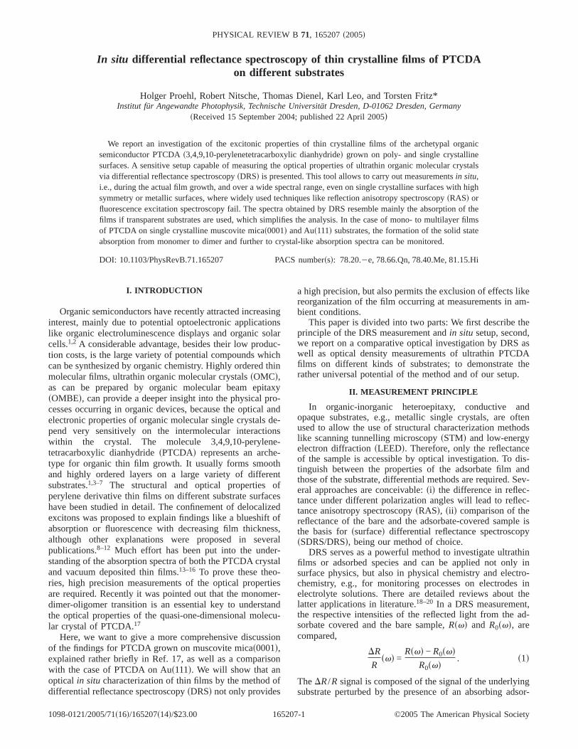
In Fig. 2, it can be seen that in case of transparent sub-strates, the DRS signal represents nearly the absorbancefi.e.,the differential optical densitysDODd, given by the differ-ence of the absorbance of the sample before and after filmdepositiong of the thin adsorbate film. A linearization of thecorresponding Fresnel equations for the case of ultrathinfilms yields for the differential optical densityDOD of theadsorbate film, an equation directly proportional to Imse2dstransparent incoherent thick substrated24
DOD >1
lns10dDT
T>
4pd2
l lns10dImse2d1 + n3
. s5d
Even in the case of thin substratessincluding backside reflec-tiond this proportionality will hold, whereas in case of thick
FIG. 1. Reflectance of the adsorbate covered and bare sample incase ofsad an opaque substrate andsbd a transparent substrate.
FIG. 2. sColor onlined Simulated DRS of a 2 nmpolycrystallinePTCDA film on Au slower partd, on a semi-infinite mica substrate,and a mica sample of a typical thickness useds150 mmd supperpartd in comparison with the absorbance spectrasdifferential Opti-cal Density,DODd of that film foptical constants of polycrystallinePTCDA from Ref. 27g. Note the similarity betweenDR/R andDODin case of the substrate mica: only a small shift of the low energypeak at 2.22 eV of,8 meV occurs.
PROEHLet al. PHYSICAL REVIEW B 71, 165207s2005d
165207-2

films the optical density is proportional to the absorption
coefficienta2=s2v /cdImsÎe2d=4pk2/l sBeer’s lawd.As an opposite example, we discuss gold as substrate.
Gold is not only opaque, but also possesses a typical yellow-ish color, in contrast to, e.g., silver or aluminum. Therefore,one has to deal with strongly varying optical constants in thevisible wavelength range. This has a large impact on theDR/R spectra as shown in Fig. 2.25,26 To quantify this influ-ence, we will further transform Eq.s2d to
DR
R> d2hC8f1 − Rese2dg + C9 Imse2dj, s6d
where the coefficientsC8 and C9 depend only on the com-plex dielectric functione3 of the substrate, but not one2.
28
In case of the substrate gold, those coefficientsC8 andC9vary rather strongly over the wavelength range of the mea-surementsFig. 3d. Only within the low-energy range, theDR/R signal corresponds approximately to the absorptionwhereDR/R~−Imse2d=2n2k2, becauseC8 is small. On theother hand, in the energy rangeEù2.7 eV, Eq.s6d simplifiesto DR/R~n2sn2−k2d−1, here −C8 is approximately twice aslarge asC9. Therefore, the DR spectra can be directly relatedto the absorbance spectra in the low-energy range only.
III. IN SITU SETUP
A. Optical system
The opticalin situ setup is implemented in a 3 chamberOMBE system described elsewhere.29 It is intended to beUHV compatible and to cover a large wavelength range as anuniversal tool for a large variety of adsorbate systems. Awavelength range of 200 to 1000 nmscorresponding to anenergy range of 6.2–1.2 eVd was desired, therefore common
achromatic single lenses could not be used. Additionally, weaim at a small detection area on the sample and a large de-tection steradian, to also enable fluorescence measurementssnot shown hered. To match this requirements, collimatingsystems with minimal chromatic aberration and a small dis-tance to the sample are needed. This is achieved by the com-bination of commercially available SiO2 concave and CaF2convex lenses inside the UHV chamber, moreover allowingan unrestricted bakeout of the system.
Figure 4sad shows the overall setup. The collimated lightbeams enter and leave the UHV chamber via SiO2 Suprasilwindows and are focused/collimated by the lens systemsLS1–LS4. In Figs. 4sbd and 4scd, a scheme of the lens sys-
FIG. 3. sColor onlined The coefficientsC8 and C9 for Au assubstrate. Two different spectral regionsE,2.1 eV withC8<0 andE,2.7 eV with C8<−2C9 can be distinguished, representing twolimiting cases of theDR/R signal composition. For comparison, inthe case of mica the coefficients have the values ofC8.0.005 andC9.40 at 2.6 eV, hence the influence of Rese2d on the DRS signalcan be neglected.
FIG. 4. sColor onlined sad Scheme of the UHV growth chamberwith the in situ DRS setup. The optical system consists mainly offour lens systems LS1–LS4 and two UV-enhanced Al mirrors M1and M2. To check for anisotropy, two polarizerssPol. +Anal.d canbe inserted.sbd The lens systems LS1, LS2, and LS4 with a frontfocal lengthsffl.d of about 163 mm consist of two commercial SiO2
and CaF2 singlets, while LS3snot shown hered, the system of ac-cumulation, has half the focal length and consists of three singlets.scd The lowest achievable chromatic aberration of the doublets LS1,LS2, and LS4 in the wavelength range of interest for the optimumlens distances.
IN SITU DIFFERENTIAL REFLECTANCE… PHYSICAL REVIEW B 71, 165207s2005d
165207-3
tems and the corresponding chromatic aberration are shown.The deviation from optical isotropy caused by the influenceof the optical elements is smaller than ±10% in the visiblewavelength range. The area of investigation on the sample isabout 0.5–0.75 mm2, the angle of incidence is about 20°.
B. Recording of spectra
An optical multichannel analyzersOMAd consisting of agrating-mirror spectrographsActon Research SpectraPro-150, 300 g/mm blazed gratingd with a CCD allows a fastspectra collection. We use a single stage peltier-cooled back-illuminated CCDsRoper Scientific, SpectruMM 250Bd witha fast 16 bit AD interfaces100 kHz sampling rated. Besidesits high sensitivity, it exhibits a relatively large dark noise of,0.4% sper single acquisitiond at maximal possible illumi-nation, caused by a minimal achievable detector temperatureof typical −35 °C only. The 16 bit interface limits the count-ing rate to 216 maximum counts per channel, which impliesan additional statistical noiseDN/N=ÎN−1 of at least,0.4%at full load, which further increases at lower light intensities.Compared to that, the noise of the A/D conversionsten elec-tronsd is negligible.
Therefore, we accumulate the signal of several successiveacquisitionsstypical 500–1600d to improve the signal-to-noise ratio ofDR by a factor of approx. 20–40, which isnecessary to investigatessubdmonolayers of adsorbed speciesssee belowd. Nevertheless, we achieve short measuring timesof 20–50 s by a continuous light exposure of the CCD, withno extra delays, hence the exposure time of a CCD line isdetermined by the read-out time.30 This enables us to carryout in situ real-time measurements during the film growth,with the implication that our spectra represent an averageover a certain film thickness range, depending on both thedeposition rate and the measuring timessee belowd.
IV. APPLICATION TO ULTRATHIN PTCDA FILMS
A. Experiment
The PTCDA films were deposited under ultrahigh vacuumsUHVd conditions by evaporation from a low flux Knudsen-type effusion cell at a cell temperature of,330 °C and avapor pressure of,3310−9 mbar. The evaporation wasdone after a thorough degassing of the cell at 200 °C. ThePTCDA deposition flux was about 0.2 ML molecular layerssML d per minute and checked by a quartz microbalance.However, the exact growth rate has been determined by op-tical meansssee belowd.
During and after the film deposition, the substrate waskept at room temperature. For every new experiment, either afreshly cleaved sheet of micasTed Pella Inc., Hi-Graded,which was extensively degassed in UHV at 150–180 °C for1–2 h to remove the water film and other contaminants fromthe surface, or an Ar+ sputtereds600 eVd and annealeds600 °Cd Aus111d single crystal was used.
The DR spectra were collected with the setup describedabove. As a source of unpolarized light we used a quartztungsten halogen lamp. For each spectrum, 1500 successiveacquisitions were averaged, corresponding to a total measur-
ing time of about 40–45 s. The spectra were corrected formechanical drift of the setup and thermal drift of the lightsource by analyzing theDR/R spectra series obtained beforeand after the deposition process. In most cases, these seriescould certify the assumption of a spectral constant drift overtime, making a drift correction of the spectra possible. AShimadzu spectrophotometersUV-3101 PCd was utilized forthe ex situabsorbance measurements.
B. Optical spectra and discussion
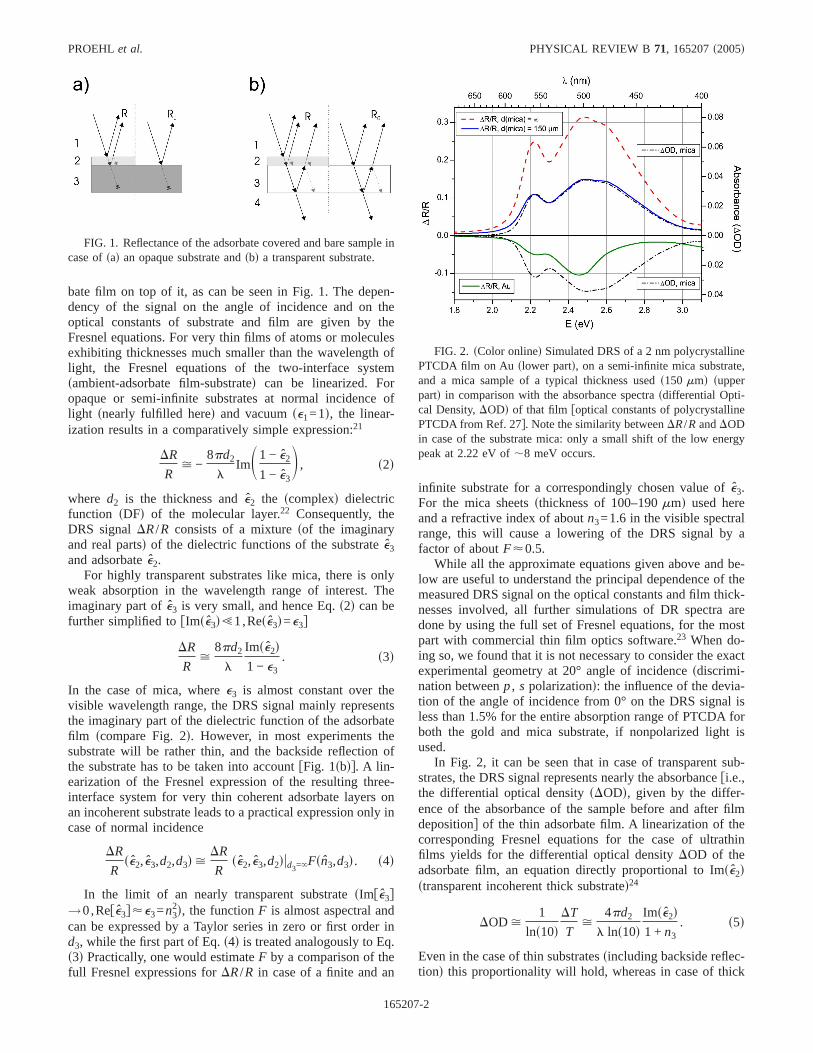
In this section, we describe and discuss both theDR/R-and the absorbance spectra obtained for PTCDA grown ondifferent substrates, after giving a short introduction in theproperties of PTCDA single crystals. The PTCDA crystals ofboth thea and theb modification exhibit a strong anisotropyin their electronic and optical properties due to a denselypacked arrangement of the molecules.1 The interaction in thecrystal can be described by discriminating between two typesof physical dimers,A andB. The molecules in theA dimers,building up the crystals102d bulk plane, are arranged in theherringbonesHBd structure as predominantly found in ultra-thin PTCDA films, and interact rather weakly. The moleculesin the p-stacked dimerB exhibit a large magnitude of inter-action. Those nearly perpendicularly arranged molecularstacks represent “molecular chains” and dominate the opticaland electronic properties of the highly anisotropic PTCDAcrystal scompare Fig. 5d.33 Therefore, PTCDA can be re-garded as a quasi-one-dimensional crystal. From excitontheories, it is known that the properties of such one-dimensional stacks depend strongly on the chain length,where a chain length of 4 already approximates an infinitechain quite nicely.16 Hence, we expect a strong dependence
FIG. 5. sColor onlined Views of the PTCDA crystalsa modifi-cationd: s100d planestopd, s001d planesrightd, ands010d planesbot-tomd. A unit cell and the two types of PTCDA dimers,A sin planedand B sout of plane, i.e., stackedd, are indicated. The unit cell di-mensions area=3.72 Å, b=11.96 Å, andc=17.34 Å. Crystal datawere taken from Refs. 31 and 32.
PROEHLet al. PHYSICAL REVIEW B 71, 165207s2005d
165207-4
of the absorption spectra on the layer thickness in the experi-mental range investigated in this work.
1. PTCDA on mica
Muscovite mica, KAl2sAl,Si3dO10sOHd2, is an easycleaveable sheet silicate, transparent in the visible. Aftercleavage, one obtains many square microns of atomically flats0001d surfaces, with a surface mesh of a,5.25 Å latticeconstant. The almost inert mica surface is well suited as asubstrate for deposition studies; here the reader is referred toliterature, i.e., Refs. 34–36.
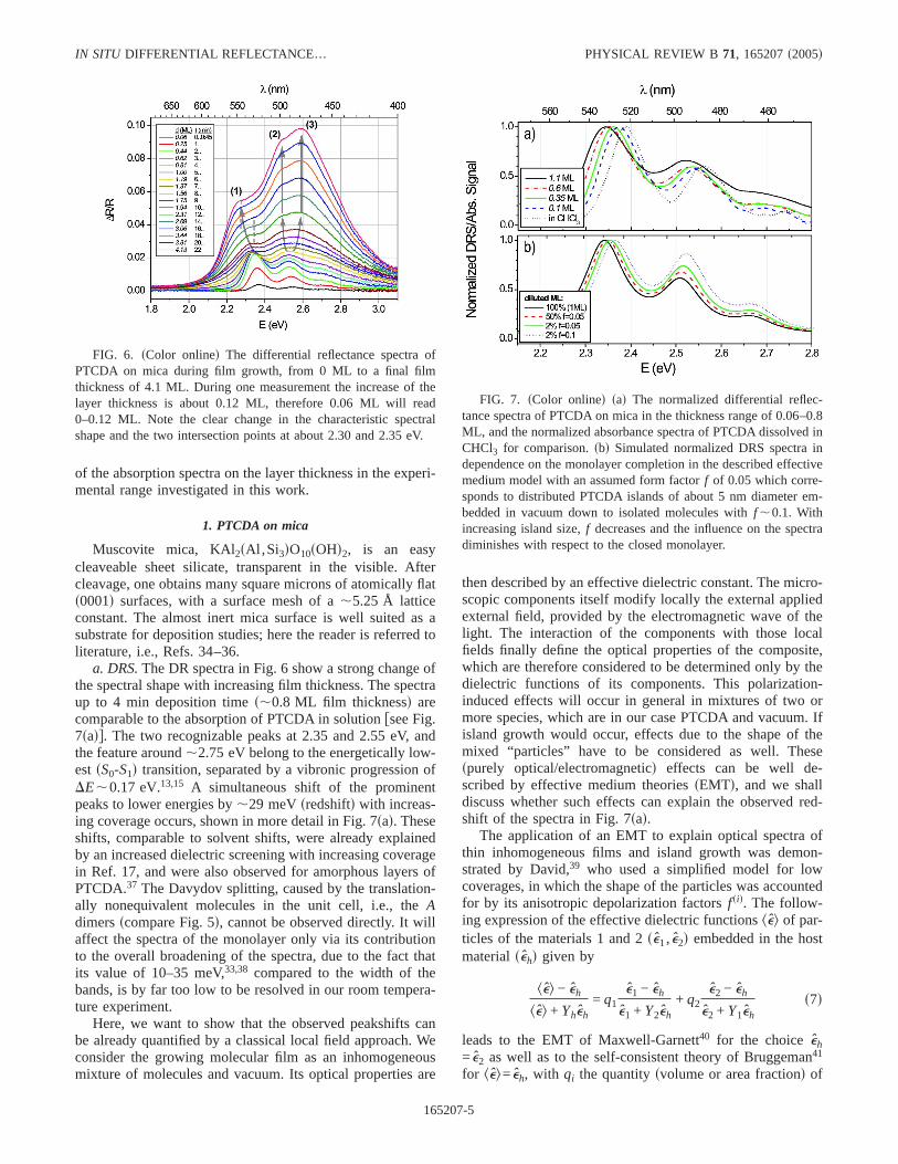
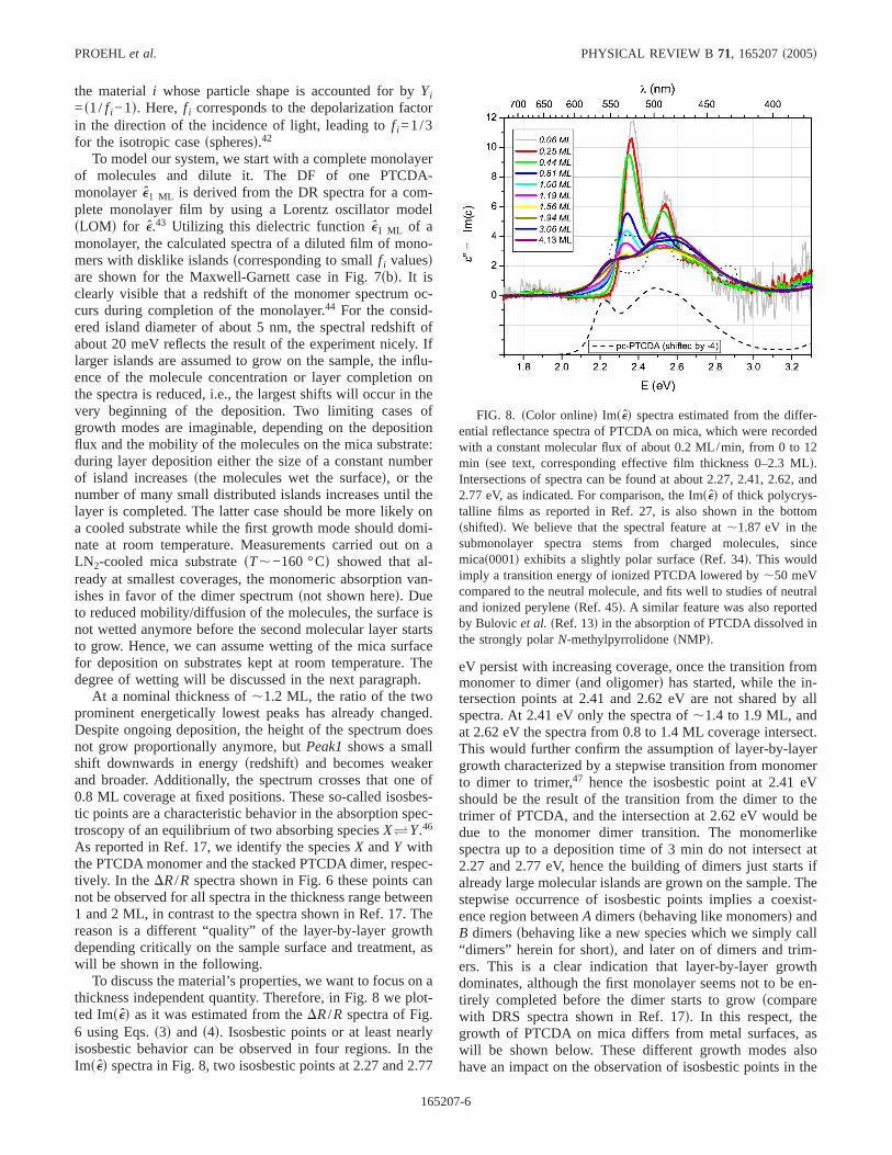
a. DRS.The DR spectra in Fig. 6 show a strong change ofthe spectral shape with increasing film thickness. The spectraup to 4 min deposition times,0.8 ML film thicknessd arecomparable to the absorption of PTCDA in solutionfsee Fig.7sadg. The two recognizable peaks at 2.35 and 2.55 eV, andthe feature around,2.75 eV belong to the energetically low-est sS0-S1d transition, separated by a vibronic progression ofDE,0.17 eV.13,15 A simultaneous shift of the prominentpeaks to lower energies by,29 meVsredshiftd with increas-ing coverage occurs, shown in more detail in Fig. 7sad. Theseshifts, comparable to solvent shifts, were already explainedby an increased dielectric screening with increasing coveragein Ref. 17, and were also observed for amorphous layers ofPTCDA.37 The Davydov splitting, caused by the translation-ally nonequivalent molecules in the unit cell, i.e., theAdimersscompare Fig. 5d, cannot be observed directly. It willaffect the spectra of the monolayer only via its contributionto the overall broadening of the spectra, due to the fact thatits value of 10–35 meV,33,38 compared to the width of thebands, is by far too low to be resolved in our room tempera-ture experiment.
Here, we want to show that the observed peakshifts canbe already quantified by a classical local field approach. Weconsider the growing molecular film as an inhomogeneousmixture of molecules and vacuum. Its optical properties are
then described by an effective dielectric constant. The micro-scopic components itself modify locally the external appliedexternal field, provided by the electromagnetic wave of thelight. The interaction of the components with those localfields finally define the optical properties of the composite,which are therefore considered to be determined only by thedielectric functions of its components. This polarization-induced effects will occur in general in mixtures of two ormore species, which are in our case PTCDA and vacuum. Ifisland growth would occur, effects due to the shape of themixed “particles” have to be considered as well. Thesespurely optical/electromagneticd effects can be well de-scribed by effective medium theoriessEMTd, and we shalldiscuss whether such effects can explain the observed red-shift of the spectra in Fig. 7sad.
The application of an EMT to explain optical spectra ofthin inhomogeneous films and island growth was demon-strated by David,39 who used a simplified model for lowcoverages, in which the shape of the particles was accountedfor by its anisotropic depolarization factorsf sid. The follow-ing expression of the effective dielectric functionskel of par-ticles of the materials 1 and 2se1, e2d embedded in the hostmaterialsehd given by
kel − eh
kel + Yheh
= q1e1 − eh
e1 + Y2eh
+ q2e2 − eh
e2 + Y1eh
s7d
leads to the EMT of Maxwell-Garnett40 for the choiceeh= e2 as well as to the self-consistent theory of Bruggeman41
for kel= eh, with qi the quantitysvolume or area fractiond of
FIG. 6. sColor onlined The differential reflectance spectra ofPTCDA on mica during film growth, from 0 ML to a final filmthickness of 4.1 ML. During one measurement the increase of thelayer thickness is about 0.12 ML, therefore 0.06 ML will read0–0.12 ML. Note the clear change in the characteristic spectralshape and the two intersection points at about 2.30 and 2.35 eV.
FIG. 7. sColor onlined sad The normalized differential reflec-tance spectra of PTCDA on mica in the thickness range of 0.06–0.8ML, and the normalized absorbance spectra of PTCDA dissolved inCHCl3 for comparison.sbd Simulated normalized DRS spectra independence on the monolayer completion in the described effectivemedium model with an assumed form factorf of 0.05 which corre-sponds to distributed PTCDA islands of about 5 nm diameter em-bedded in vacuum down to isolated molecules withf ,0.1. Withincreasing island size,f decreases and the influence on the spectradiminishes with respect to the closed monolayer.
IN SITU DIFFERENTIAL REFLECTANCE… PHYSICAL REVIEW B 71, 165207s2005d
165207-5
the materiali whose particle shape is accounted for byYi=s1/ f i −1d. Here, f i corresponds to the depolarization factorin the direction of the incidence of light, leading tof i =1/3for the isotropic casesspheresd.42
To model our system, we start with a complete monolayerof molecules and dilute it. The DF of one PTCDA-monolayere1 ML is derived from the DR spectra for a com-plete monolayer film by using a Lorentz oscillator modelsLOMd for e.43 Utilizing this dielectric functione1 ML of amonolayer, the calculated spectra of a diluted film of mono-mers with disklike islandsscorresponding to smallf i valuesdare shown for the Maxwell-Garnett case in Fig. 7sbd. It isclearly visible that a redshift of the monomer spectrum oc-curs during completion of the monolayer.44 For the consid-ered island diameter of about 5 nm, the spectral redshift ofabout 20 meV reflects the result of the experiment nicely. Iflarger islands are assumed to grow on the sample, the influ-ence of the molecule concentration or layer completion onthe spectra is reduced, i.e., the largest shifts will occur in thevery beginning of the deposition. Two limiting cases ofgrowth modes are imaginable, depending on the depositionflux and the mobility of the molecules on the mica substrate:during layer deposition either the size of a constant numberof island increasessthe molecules wet the surfaced, or thenumber of many small distributed islands increases until thelayer is completed. The latter case should be more likely ona cooled substrate while the first growth mode should domi-nate at room temperature. Measurements carried out on aLN2-cooled mica substratesT,−160 °Cd showed that al-ready at smallest coverages, the monomeric absorption van-ishes in favor of the dimer spectrumsnot shown hered. Dueto reduced mobility/diffusion of the molecules, the surface isnot wetted anymore before the second molecular layer startsto grow. Hence, we can assume wetting of the mica surfacefor deposition on substrates kept at room temperature. Thedegree of wetting will be discussed in the next paragraph.
At a nominal thickness of,1.2 ML, the ratio of the twoprominent energetically lowest peaks has already changed.Despite ongoing deposition, the height of the spectrum doesnot grow proportionally anymore, butPeak1shows a smallshift downwards in energysredshiftd and becomes weakerand broader. Additionally, the spectrum crosses that one of0.8 ML coverage at fixed positions. These so-called isosbes-tic points are a characteristic behavior in the absorption spec-troscopy of an equilibrium of two absorbing speciesXY.46
As reported in Ref. 17, we identify the speciesX andY withthe PTCDA monomer and the stacked PTCDA dimer, respec-tively. In theDR/R spectra shown in Fig. 6 these points cannot be observed for all spectra in the thickness range between1 and 2 ML, in contrast to the spectra shown in Ref. 17. Thereason is a different “quality” of the layer-by-layer growthdepending critically on the sample surface and treatment, aswill be shown in the following.
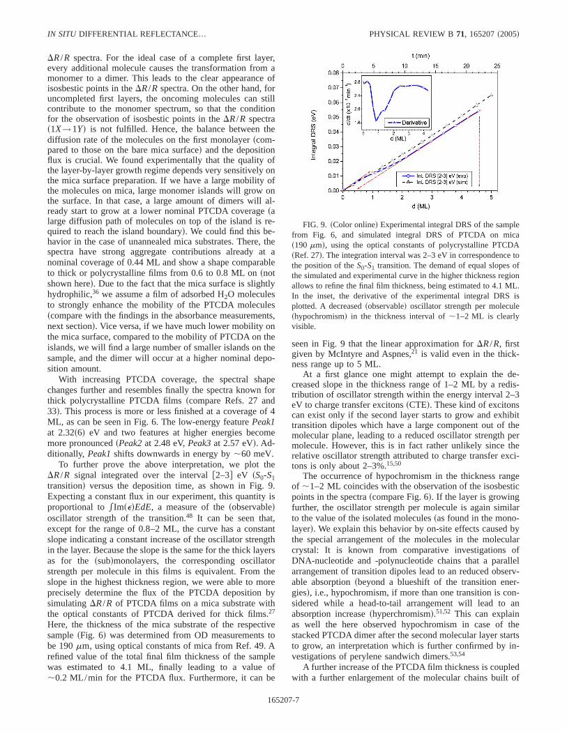
To discuss the material’s properties, we want to focus on athickness independent quantity. Therefore, in Fig. 8 we plot-ted Imsed as it was estimated from theDR/R spectra of Fig.6 using Eqs.s3d and s4d. Isosbestic points or at least nearlyisosbestic behavior can be observed in four regions. In theImsed spectra in Fig. 8, two isosbestic points at 2.27 and 2.77
eV persist with increasing coverage, once the transition frommonomer to dimersand oligomerd has started, while the in-tersection points at 2.41 and 2.62 eV are not shared by allspectra. At 2.41 eV only the spectra of,1.4 to 1.9 ML, andat 2.62 eV the spectra from 0.8 to 1.4 ML coverage intersect.This would further confirm the assumption of layer-by-layergrowth characterized by a stepwise transition from monomerto dimer to trimer,47 hence the isosbestic point at 2.41 eVshould be the result of the transition from the dimer to thetrimer of PTCDA, and the intersection at 2.62 eV would bedue to the monomer dimer transition. The monomerlikespectra up to a deposition time of 3 min do not intersect at2.27 and 2.77 eV, hence the building of dimers just starts ifalready large molecular islands are grown on the sample. Thestepwise occurrence of isosbestic points implies a coexist-ence region betweenA dimerssbehaving like monomersd andB dimerssbehaving like a new species which we simply call“dimers” herein for shortd, and later on of dimers and trim-ers. This is a clear indication that layer-by-layer growthdominates, although the first monolayer seems not to be en-tirely completed before the dimer starts to growscomparewith DRS spectra shown in Ref. 17d. In this respect, thegrowth of PTCDA on mica differs from metal surfaces, aswill be shown below. These different growth modes alsohave an impact on the observation of isosbestic points in the
FIG. 8. sColor onlined Imsed spectra estimated from the differ-ential reflectance spectra of PTCDA on mica, which were recordedwith a constant molecular flux of about 0.2 ML/min, from 0 to 12min ssee text, corresponding effective film thickness 0–2.3 MLd.Intersections of spectra can be found at about 2.27, 2.41, 2.62, and2.77 eV, as indicated. For comparison, the Imsed of thick polycrys-talline films as reported in Ref. 27, is also shown in the bottomsshiftedd. We believe that the spectral feature at,1.87 eV in thesubmonolayer spectra stems from charged molecules, sincemicas0001d exhibits a slightly polar surfacesRef. 34d. This wouldimply a transition energy of ionized PTCDA lowered by,50 meVcompared to the neutral molecule, and fits well to studies of neutraland ionized perylenesRef. 45d. A similar feature was also reportedby Bulovic et al. sRef. 13d in the absorption of PTCDA dissolved inthe strongly polarN-methylpyrrolidonesNMPd.
PROEHLet al. PHYSICAL REVIEW B 71, 165207s2005d
165207-6
DR/R spectra. For the ideal case of a complete first layer,every additional molecule causes the transformation from amonomer to a dimer. This leads to the clear appearance ofisosbestic points in theDR/R spectra. On the other hand, foruncompleted first layers, the oncoming molecules can stillcontribute to the monomer spectrum, so that the conditionfor the observation of isosbestic points in theDR/R spectras1X→1Yd is not fulfilled. Hence, the balance between thediffusion rate of the molecules on the first monolayerscom-pared to those on the bare mica surfaced and the depositionflux is crucial. We found experimentally that the quality ofthe layer-by-layer growth regime depends very sensitively onthe mica surface preparation. If we have a large mobility ofthe molecules on mica, large monomer islands will grow onthe surface. In that case, a large amount of dimers will al-ready start to grow at a lower nominal PTCDA coveragesalarge diffusion path of molecules on top of the island is re-quired to reach the island boundaryd. We could find this be-havior in the case of unannealed mica substrates. There, thespectra have strong aggregate contributions already at anominal coverage of 0.44 ML and show a shape comparableto thick or polycrystalline films from 0.6 to 0.8 ML onsnotshown hered. Due to the fact that the mica surface is slightlyhydrophilic,36 we assume a film of adsorbed H2O moleculesto strongly enhance the mobility of the PTCDA moleculesscompare with the findings in the absorbance measurements,next sectiond. Vice versa, if we have much lower mobility onthe mica surface, compared to the mobility of PTCDA on theislands, we will find a large number of smaller islands on thesample, and the dimer will occur at a higher nominal depo-sition amount.
With increasing PTCDA coverage, the spectral shapechanges further and resembles finally the spectra known forthick polycrystalline PTCDA filmsscompare Refs. 27 and33d. This process is more or less finished at a coverage of 4ML, as can be seen in Fig. 6. The low-energy featurePeak1at 2.32s6d eV and two features at higher energies becomemore pronouncedsPeak2at 2.48 eV,Peak3at 2.57 eVd. Ad-ditionally, Peak1shifts downwards in energy by,60 meV.
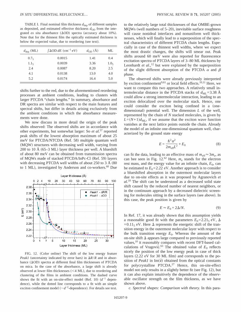
To further prove the above interpretation, we plot theDR/R signal integrated over the intervalf2–3g eV sS0-S1transitiond versus the deposition time, as shown in Fig. 9.Expecting a constant flux in our experiment, this quantity isproportional toeImsedEdE, a measure of thesobservabledoscillator strength of the transition.48 It can be seen that,except for the range of 0.8–2 ML, the curve has a constantslope indicating a constant increase of the oscillator strengthin the layer. Because the slope is the same for the thick layersas for the ssubdmonolayers, the corresponding oscillatorstrength per molecule in this films is equivalent. From theslope in the highest thickness region, we were able to moreprecisely determine the flux of the PTCDA deposition bysimulatingDR/R of PTCDA films on a mica substrate withthe optical constants of PTCDA derived for thick films.27
Here, the thickness of the mica substrate of the respectivesamplesFig. 6d was determined from OD measurements tobe 190mm, using optical constants of mica from Ref. 49. Arefined value of the total final film thickness of the samplewas estimated to 4.1 ML, finally leading to a value of,0.2 ML/min for the PTCDA flux. Furthermore, it can be
seen in Fig. 9 that the linear approximation forDR/R, firstgiven by McIntyre and Aspnes,21 is valid even in the thick-ness range up to 5 ML.
At a first glance one might attempt to explain the de-creased slope in the thickness range of 1–2 ML by a redis-tribution of oscillator strength within the energy interval 2–3eV to charge transfer excitonssCTEd. These kind of excitonscan exist only if the second layer starts to grow and exhibittransition dipoles which have a large component out of themolecular plane, leading to a reduced oscillator strength permolecule. However, this is in fact rather unlikely since therelative oscillator strength attributed to charge transfer exci-tons is only about 2–3%.15,50
The occurrence of hypochromism in the thickness rangeof ,1–2 ML coincides with the observation of the isosbesticpoints in the spectrascompare Fig. 6d. If the layer is growingfurther, the oscillator strength per molecule is again similarto the value of the isolated moleculessas found in the mono-layerd. We explain this behavior by on-site effects caused bythe special arrangement of the molecules in the molecularcrystal: It is known from comparative investigations ofDNA-nucleotide and -polynucleotide chains that a parallelarrangement of transition dipoles lead to an reduced observ-able absorptionsbeyond a blueshift of the transition ener-giesd, i.e., hypochromism, if more than one transition is con-sidered while a head-to-tail arrangement will lead to anabsorption increaseshyperchromismd.51,52 This can explainas well the here observed hypochromism in case of thestacked PTCDA dimer after the second molecular layer startsto grow, an interpretation which is further confirmed by in-vestigations of perylene sandwich dimers.53,54
A further increase of the PTCDA film thickness is coupledwith a further enlargement of the molecular chains built of
FIG. 9. sColor onlined Experimental integral DRS of the samplefrom Fig. 6, and simulated integral DRS of PTCDA on micas190 mmd, using the optical constants of polycrystalline PTCDAsRef. 27d. The integration interval was 2–3 eV in correspondence tothe position of theS0-S1 transition. The demand of equal slopes ofthe simulated and experimental curve in the higher thickness regionallows to refine the final film thickness, being estimated to 4.1 ML.In the inset, the derivative of the experimental integral DRS isplotted. A decreasedsobservabled oscillator strength per moleculeshypochromismd in the thickness interval of,1–2 ML is clearlyvisible.
IN SITU DIFFERENTIAL REFLECTANCE… PHYSICAL REVIEW B 71, 165207s2005d
165207-7

stacked PTCDA molecules, although no additional type ofinteraction comes into play. Here, we have to keep in mindthat on-site effects like the shift of the transition energies dueto a reduced number of nearest neighbors in the outermostmolecular layers of the film were used to explain effects likethe blueshift of absorption in case of ultrathin filmssseebelowd.10,17Those shifts of absorption energies can be under-stood classically by a decreased dielectric screening in theoutermost molecular layers. However, we have to remindthat a reduced background dielectric screening also decreasesthe observable oscillator strength of a certain transition.48 Itis generally acknowledged that the dielectric constant of abulk crystal develops at length scales comparable to thenearest-neighbor-distances, in our case the stackingdistance.9,50 Hence, in case of a stacking length of alreadyNù3, we can consider for the innermost molecules a dielec-tric screening like in the bulk material. If the PTCDA chainlength exceedsN=3, the number of innermost molecules in-creases, showing a stronger absorption compared to the out-ermost molecular layer. In our case, the resulting slope of theeDR/RdE curve becomes steeper and correspondsswithinthe limits of the experimental accuracyd to the slope in thesubmonolayer region.
Due to the fact that the slope of the curve of the experi-mental DRS does not significantly decrease with increasingfilm thickness, we can exclude an increased roughening ofthe film up to a thickness of 4 ML.
b. Absorbance.To relate thein situ DRS results to a com-mon method and other reported results, the samples of dif-ferent final thickness were transferred out of the UHV sys-tem to measure their absorbanceex situ. The differentialoptical density of the PTCDA film was estimated by sub-tracting the absorbance of the mica substratesas measuredbefore transferring them into UHVd from the film coveredsample.
The shape of the absorbance spectra is equivalent to theDRS spectra in case of films thicker than 2–3 ML as can beseen in Fig. 10. With decreasing thickness, even if the filmsbecome as thin as 1–2 ML, the absorbance spectra keep theirpolycrystalline character. This suggests that the film is reor-dering at ambient conditions while transferring the sample tothe transmittance measurement setup. The catalyst seems tobe a film of adsorbed water, which stems from the atmo-spheric moisture. To prove this assumption, the sample wasrapidly transferred to the spectrophotometer by using an ex-siccator, after venting the transfer load lock with dry nitro-gen. The transmittance was then measured in the spectropho-tometer which was previously prepared with desiccant, too,to reduce the humidity inside. The time dependence of theabsorption spectra could therefore be resolved and is shownin Fig. 11, which confirms the assumption proposed above.Due to clustering, not onlyPeak1but the overall OD is re-duced, as can be seen in Table I.56 For films thicker than 2ML, no time dependence of the transmittance on these timescales could be observed. Nevertheless, a comparison of thethickness values of the films with the highest final coveragesin Table I shows a slightly lowerex situ absorbance thanexpected, leading to the assumption that at ambient condi-tions additional roughness due to clustering at the film sur-face may occur.
In Fig. 12, the shift ofPeak1in both DRS and absorbanceis plotted versus the film thickness. Two different slopes ofthe shift can be clearly identified. With decreasing thicknessdown to 4 ML, only a small shift of about 40 meV ofPeak1occurs, whereas in the coverage range of 3–1 ML it extendsto ,65 meV. The shifts in OD and DRS are very well com-parable, except for the thinnest films. In this case,Peak1
FIG. 10. sColor onlined The absorption spectrasDOD, left yaxisd of investigated PTCDA on mica films with different finalthickness from 0.4 to 5.2 ML. In case of the 5.2 ML sample theDR/R spectrum is shown for comparisonsright y axisd. The differ-ential optical density of the films was determined by the differenceof the optical density of the sample before and after film deposition.The shape of theDOD spectra remains constant even when thenominal film thickness becomes as thin as 1 ML.
FIG. 11. sColor onlined The time dependence of theDOD spec-tra of ,0.75 ML PTCDA in a desiccated spectrophotometer. Thetime t=0 corresponds to the first measurement after the transferfrom the vacuum lock into the spectrophotometer in an exsiccatorsthe duration is,3 mind. The spectra were noise filtered by themethod of LeesRef. 55d swindow size=5d. Due to the small thick-ness of the mica substrate, small interference modulations are vis-ible in the spectra. In measurements after 24 hsnot shown hered,Peak1was found redshifted by 17 meV. For comparison, theDR/Rsignal of the sample is also shownsgray line, right scaled.
PROEHLet al. PHYSICAL REVIEW B 71, 165207s2005d
165207-8
shifts further to the red, due to the aforementioned reorderingprocesses at ambient conditions, leading to clusters withlarger PTCDA “chain lengths.” In summary, absorbance andDR spectra are similar with respect to the main features andspectral shifts, but differ in details arising exclusively fromthe ambient conditions in which the absorbance measure-ments were done.
We now discuss in more detail the origin of the peakshifts observed: The observed shifts are in accordance withother experiments, but somewhat larger: Soet al.57 reportedpeak shifts of the lowest absorption maximum of about 25meV for PTCDA/NTCDAsRef. 58d multiple quantum wellsMQWd structures with decreasing well width, varying from200 to 10 Ås65–3 MLd layer thickness per well. A blueshiftof about 80 meV can be obtained from transmission spectraof MQWs made of stacked PTCDA/InPc-ClsRef. 59d layerswith decreasing PTCDA well widths of about 250 to 3 Ås80to 1 MLd, investigated by Anderson and co-workers.60 Due
to the relatively large total thicknesses of that OMBE-grownMQWs swell numbers of 5–20d, inevitable surface roughnesswill cause nonideal interfaces and nonuniform well thick-nesses, which will finally lead to a superposition of the spec-tral characteristics of different PTCDA chain lengths. Espe-cially in case of the thinnest well widths, where we expectthe most drastic changes, the shifts will smear out. Peakshifts around 60 meV were also reported for fluorescenceexcitation spectra of PTCDA layers of 3–80 ML thickness byLeonhardtet al.,12 but were explained by the superpositionof the slight different absorption of the PTCDAa and bphase.
The observed shifts were already previously interpretedby exciton confinement9,61 or local field effects.10,11Here, wewant to compare this two approaches. A relatively small in-termolecular distance in the PTCDA stacks ofdML =3.38 Åcould allow a strong intermolecular interaction, leading to anexciton delocalized over the molecular stack. Hence, onecould consider the exciton being confined in asone-dimensionald potential well. The dimensionL of the well,represented by the chain ofN stacked molecules, is given byL=sN+1ddML, if we assume that the exciton wave functionvanishes at the next lattice points outside the chain. Alreadythe model of an infinite one-dimensional quantum well, char-acterized by the ground state energy
E ="2p2
2meffL2 + E0 s8d
can fit the data, leading to an effective mass ofmeff<3me, ascan bee seen in Fig. 12.62 Here, me stands for the electronrest mass, and the energy value for an infinite chain,E0, canbe estimated toE0=2.22 eV. Another approach is to considera blueshifted absorption in the outermost molecular layersdue to on-site effects as it was proposed by Agranovichetal.10 The shift can be understood as a decreased solid stateshift caused by the reduced number of nearest neighbors, orin the continuum approach by a decreased dielectric screen-ing for molecules sitting in the surface layersssee aboved. Inthis case, the peak position is given by
E < E0 + 2D/N. s9d
In Ref. 17, it was already shown that this assumption yieldsa reasonable good fit with the parametersE0=2.215 eV, D=0.115 eV. HereD represents the energetic shift of the tran-sition energy in the outermost molecular layer with respect tothe bulk transition energyE0. Whereas the amount of theon-site shiftD appears large compared to previously reportedvalues,10 it reasonably compares with recent DFT-based cal-culations of Vragović.63 The obtained value ofE0 reflectsnicely the position of the low energy peak in case of thicklayerss2.22 eV for 30 ML filmd and corresponds to the po-sition of Peak1in Imsed obtained from the optical constantsfor polycrystalline PTCDA.27 Hence, this on-site-effectmodel not only results in a slightly better fitssee Fig. 12d, butit can also explain intuitively the dependence of the observ-able oscillator strength on the film thickness, as we haveshown above.
c. Spectral shapes: Comparison with theory.In this para-
TABLE I. Final nominal film thicknessddepof different samplesas deposited, and estimated effective thicknessdOD from the inte-grated ex situ absorbancesDODd spectrasaccuracy about 10%d.Note that for the thinnest film the optically estimated thickness isbelow the expected value, due to reorderingssee textd.
ddep sML d eDOD dE scm−1 eVd dOD sÅd ML
0.75 0.0015 1.41 0.4
1.15 0.0039 3.36 1.052.4 0.0087 8.20 2.5
4.1 0.0138 13.0 4.0
5.2 0.0174 16.4 5.0
FIG. 12. sColor onlined The shift of the low energy featurePeak1suncertainty indicated by error barsd in DR/R and in absor-bancesDODd spectra at different final film thicknesses of PTCDAon mica. In the case of the absorbance, a large shift is alreadyobserved at lower film thicknessess,4 MLd, due to reordering andclustering of the films in ambient conditions. The dashed curveshows the fit with an on-site-effect modelsRef. 10d sd−1 depen-denced, while the dotted line corresponds to a fit with an simpleexciton confinement models,d−2-dependenced. For details see text.
IN SITU DIFFERENTIAL REFLECTANCE… PHYSICAL REVIEW B 71, 165207s2005d
165207-9

graph, we want to compare the shape of the spectra, espe-cially of the stacked PTCDA dimer, with the spectra obtainedby recent model calculations. As we described above, al-ready the PTCDA stacked dimersB dimerd has a spectralshape near that of thesthickd film. This surprising finding canbe related to an early publication of Ferguson:53 He investi-gated sandwich dimers of perylenesthe unit corresponding tothe chromophore core of PTCDAd and found drastic spectralchanges between the monomer and the dimer absorption, thelatter already resembling the absorption of the molecularcrystal inb modification.64 This can support our findings incase of PTCDA, where to our knowledge no spectroscopicinvestigations of defined aggregates exist. Investigations oflinearly arranged perylene chromophoressinterconnectedperylene-mono-carboximide unitsd, reported by Christetal.,65 showed an absorption with the spectral shape of a cor-responding monomer, but slightly redshifted, as expected fora head to tail arrangement of transition moments. This con-firms the finding of a weak interaction in the PTCDA mono-layer, yielding to a monomeric spectral shape.
A microscopic calculation of the spectroscopic propertiesof PTCDA ultrathin films was presented by Vragovic in Ref.63. This description, originated from a pure Frenkel excitonmodel for the PTCDA crystal14,50 is based on DFT-derivedparameters including on-site shifts, and yields the Imsedshown in Fig. 13sad. The spectral changes occurring withincreasing film thickness are obvious, but the transition frommonomer to the thin film spectra occurs in a thickness rangemuch larger than observed here. Hence, the in-stack interac-tion seems to be underestimated. Additionally, the spectrumof the PTCDA monolayer is too much broadened, comparedto the experiment, indicating an overestimated in-plane inter-action. This broadening also results in a decreased peakheight of the 1 ML spectrum and hinders isosbestic behaviorin DR/R for the monomer dimer transitionfcompare Fig.13sad, dashed lineg.
Another model description of the PTCDA absorption wasintroduced by Hennessyet al.66,67 They could explain allspectral characteristics of the PTCDA absorption already inthe framework of a Holstein model of thesstackedd PTCDAdimer, including both, Frenkel- and charge-transfer excitons.This would correspond to the strong spectral differences be-tween the monomer and the dimer spectra in our measure-ments, the latter already resembling nearly the PTCDA thinfilm absorption. The Imsed spectrum obtained by Kramers-Kronig analysis from the simulated absorption spectrum inRef. 67 can be found in Fig. 13sbd, besides the monomerspectrum.68 If similar oscillator strength of monomer anddimer is anticipated for simplicity, it can be seen that isos-bestic behavior in Imsedd~ sDR/Rdl will result.
Finally, we will discuss the effect of roughening on thespectra of thin films, because at the highest coverages inves-tigated here, island growth cannot be excluded. To checkwhether roughness has an impact on the optical spectra, wemodeled the DRS spectra of films with different surfaceroughness. For that purpose, a PTCDA layer with an averagethickness of 2 nms6 MLd was composed of a 1 nm thicksolid and a rough surface layer on top of it. This surfacelayer is represented by a 2 nmthick film of 50% PTCDAsand 50% vacuumd with different particle shapes, described
by an EMT with different form factorsssee aboved. In Fig.14, the resulting DRS spectra in the framework of the EMTof Maxwell-Garnett are shown. The form factorf =0.33 cor-responds to spherelike particles,f =0.1 corresponds tosob-lated disks, about eight times larger in diameter than in thick-ness, whilef =0.05 corresponds to oblates with a diameter-to-thickness ratio of about 25. It is obvious that withincreasing roughness both, the height of the spectra and theirshape, are affected. With increasing form factorf, the spectrachange obviously:Peak3becomes more pronounced than inthe closed layersfor f →0, we would reach the case ofboundless islands, i.e., the case of a closed surface layer of 1nm thicknessd, although its intensity decreases. Already at asmall roughness, represented byf =0.05, the ratio ofPeak2andPeak3has changed. This observation would correspondto the different peak ratios in the experimentalDR/R spectra,
FIG. 13. sColor onlined sad Imsed spectra of PTCDA layers withthicknessN sML d obtained by Kramers-Kronig analysis from theImsnd spectra given in the work of VragovicsRef. 63d. In case ofthe monolayer, we also assumed a reduced dielectric backgroundfor PTCDA when calculating the Imsed spectrum, given by the micasubstrate witheb=2.6. For the dimer additionally the curve 23 Imsed, corresponding tosDR/Rd /E, was plotted as a dashed line.Obviously, no isosbestic behavior would be found in DRS.sbd Themonomer dimer transition according to Hennessyet al. sRef. 67d. Incontrast to the original work, we used here Imsed obtained from themodeled absorbance spectrum via Kramers-Kronig analysis, and weblueshifted the modeled spectrum by 0.11 eV, to fit the experimentalposition ofPeak1for the dimer. For the dimer, also 23 Imsed wasplotted as dashed line, resulting in isosbestic behavior even in DRS.
PROEHLet al. PHYSICAL REVIEW B 71, 165207s2005d
165207-10
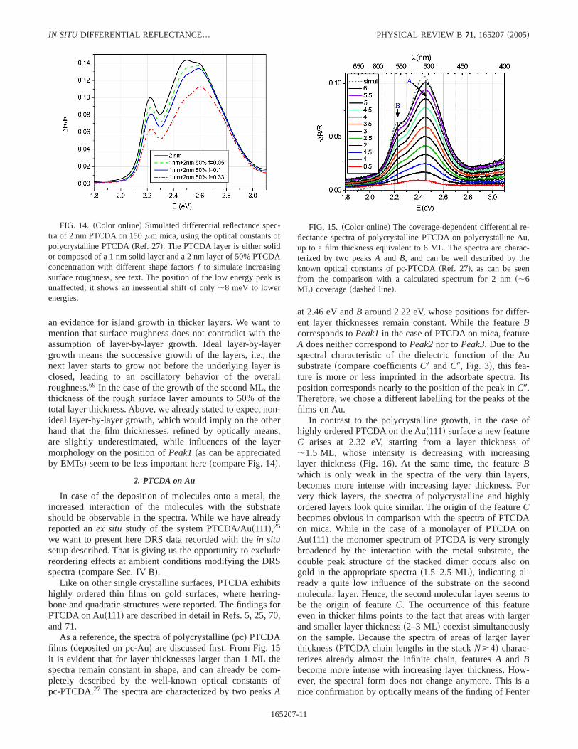
an evidence for island growth in thicker layers. We want tomention that surface roughness does not contradict with theassumption of layer-by-layer growth. Ideal layer-by-layergrowth means the successive growth of the layers, i.e., thenext layer starts to grow not before the underlying layer isclosed, leading to an oscillatory behavior of the overallroughness.69 In the case of the growth of the second ML, thethickness of the rough surface layer amounts to 50% of thetotal layer thickness. Above, we already stated to expect non-ideal layer-by-layer growth, which would imply on the otherhand that the film thicknesses, refined by optically means,are slightly underestimated, while influences of the layermorphology on the position ofPeak1sas can be appreciatedby EMTsd seem to be less important herescompare Fig. 14d.
2. PTCDA on Au
In case of the deposition of molecules onto a metal, theincreased interaction of the molecules with the substrateshould be observable in the spectra. While we have alreadyreported anex situstudy of the system PTCDA/Aus111d,25
we want to present here DRS data recorded with thein situsetup described. That is giving us the opportunity to excludereordering effects at ambient conditions modifying the DRSspectrascompare Sec. IV Bd.
Like on other single crystalline surfaces, PTCDA exhibitshighly ordered thin films on gold surfaces, where herring-bone and quadratic structures were reported. The findings forPTCDA on Aus111d are described in detail in Refs. 5, 25, 70,and 71.
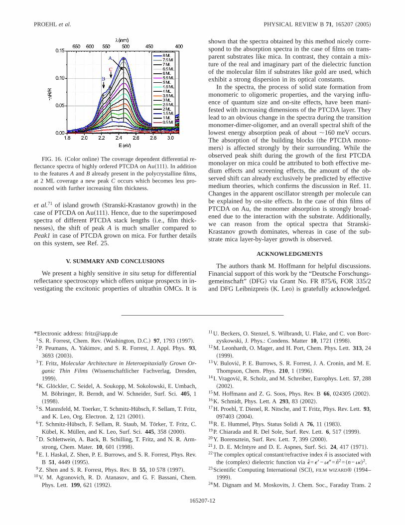
As a reference, the spectra of polycrystallinespcd PTCDAfilms sdeposited on pc-Aud are discussed first. From Fig. 15it is evident that for layer thicknesses larger than 1 ML thespectra remain constant in shape, and can already be com-pletely described by the well-known optical constants ofpc-PTCDA.27 The spectra are characterized by two peaksA
at 2.46 eV andB around 2.22 eV, whose positions for differ-ent layer thicknesses remain constant. While the featureBcorresponds toPeak1in the case of PTCDA on mica, featureA does neither correspond toPeak2nor toPeak3. Due to thespectral characteristic of the dielectric function of the Ausubstratescompare coefficientsC8 andC9, Fig. 3d, this fea-ture is more or less imprinted in the adsorbate spectra. Itsposition corresponds nearly to the position of the peak inC9.Therefore, we chose a different labelling for the peaks of thefilms on Au.
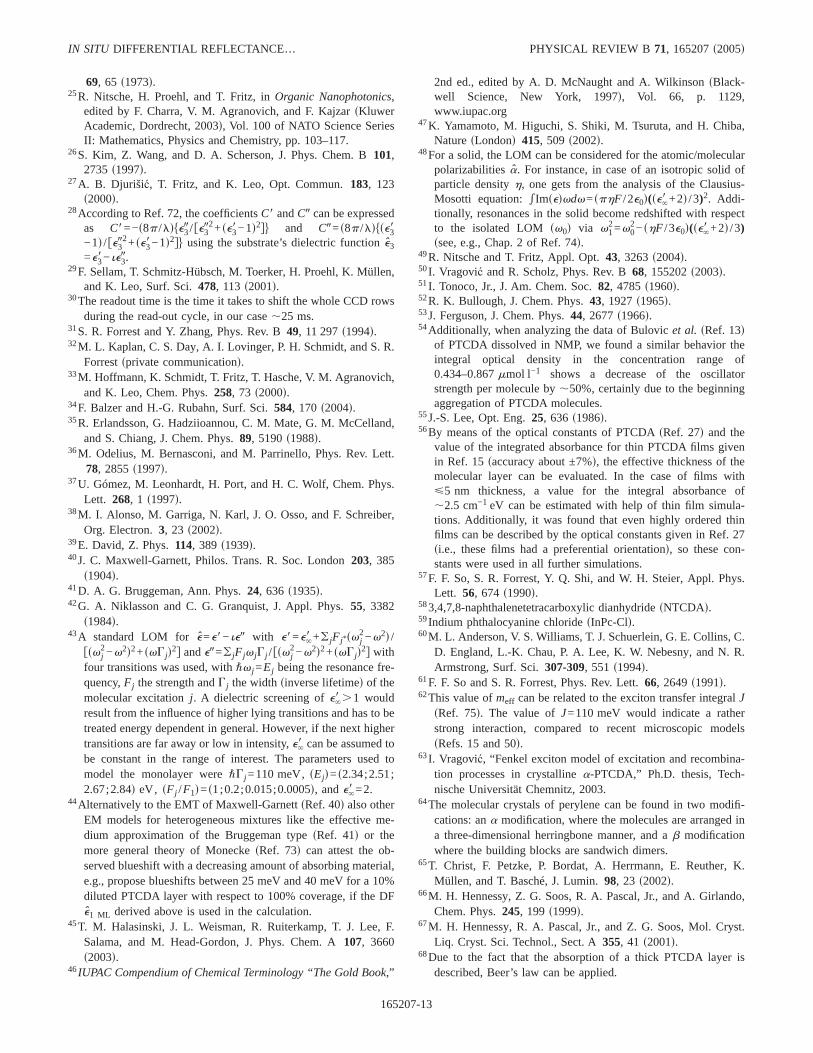
In contrast to the polycrystalline growth, in the case ofhighly ordered PTCDA on the Aus111d surface a new featureC arises at 2.32 eV, starting from a layer thickness of,1.5 ML, whose intensity is decreasing with increasinglayer thicknesssFig. 16d. At the same time, the featureBwhich is only weak in the spectra of the very thin layers,becomes more intense with increasing layer thickness. Forvery thick layers, the spectra of polycrystalline and highlyordered layers look quite similar. The origin of the featureCbecomes obvious in comparison with the spectra of PTCDAon mica. While in the case of a monolayer of PTCDA onAus111d the monomer spectrum of PTCDA is very stronglybroadened by the interaction with the metal substrate, thedouble peak structure of the stacked dimer occurs also ongold in the appropriate spectras1.5–2.5 MLd, indicating al-ready a quite low influence of the substrate on the secondmolecular layer. Hence, the second molecular layer seems tobe the origin of featureC. The occurrence of this featureeven in thicker films points to the fact that areas with largerand smaller layer thicknesss2–3 MLd coexist simultaneouslyon the sample. Because the spectra of areas of larger layerthicknesssPTCDA chain lengths in the stackNù4d charac-terizes already almost the infinite chain, featuresA and Bbecome more intense with increasing layer thickness. How-ever, the spectral form does not change anymore. This is anice confirmation by optically means of the finding of Fenter
FIG. 14. sColor onlined Simulated differential reflectance spec-tra of 2 nm PTCDA on 150mm mica, using the optical constants ofpolycrystalline PTCDAsRef. 27d. The PTCDA layer is either solidor composed of a 1 nmsolid layer and a 2 nmlayer of 50% PTCDAconcentration with different shape factorsf to simulate increasingsurface roughness, see text. The position of the low energy peak isunaffected; it shows an inessential shift of only,8 meV to lowerenergies.
FIG. 15. sColor onlined The coverage-dependent differential re-flectance spectra of polycrystalline PTCDA on polycrystalline Au,up to a film thickness equivalent to 6 ML. The spectra are charac-terized by two peaksA and B, and can be well described by theknown optical constants of pc-PTCDAsRef. 27d, as can be seenfrom the comparison with a calculated spectrum for 2 nms,6ML d coveragesdashed lined.
IN SITU DIFFERENTIAL REFLECTANCE… PHYSICAL REVIEW B 71, 165207s2005d
165207-11
et al.71 of island growthsStranski-Krastanov growthd in thecase of PTCDA on Aus111d. Hence, due to the superimposedspectra of different PTCDA stack lengthssi.e., film thick-nessesd, the shift of peakA is much smaller compared toPeak1in case of PTCDA grown on mica. For further detailson this system, see Ref. 25.
V. SUMMARY AND CONCLUSIONS
We present a highly sensitivein situ setup for differentialreflectance spectroscopy which offers unique prospects in in-vestigating the excitonic properties of ultrathin OMCs. It is
shown that the spectra obtained by this method nicely corre-spond to the absorption spectra in the case of films on trans-parent substrates like mica. In contrast, they contain a mix-ture of the real and imaginary part of the dielectric functionof the molecular film if substrates like gold are used, whichexhibit a strong dispersion in its optical constants.
In the spectra, the process of solid state formation frommonomeric to oligomeric properties, and the varying influ-ence of quantum size and on-site effects, have been mani-fested with increasing dimensions of the PTCDA layer. Theylead to an obvious change in the spectra during the transitionmonomer-dimer-oligomer, and an overall spectral shift of thelowest energy absorption peak of about,160 meV occurs.The absorption of the building blockssthe PTCDA mono-mersd is affected strongly by their surrounding. While theobserved peak shift during the growth of the first PTCDAmonolayer on mica could be attributed to both effective me-dium effects and screening effects, the amount of the ob-served shift can already exclusively be predicted by effectivemedium theories, which confirms the discussion in Ref. 11.Changes in the apparent oscillator strength per molecule canbe explained by on-site effects. In the case of thin films ofPTCDA on Au, the monomer absorption is strongly broad-ened due to the interaction with the substrate. Additionally,we can reason from the optical spectra that Stranski-Krastanov growth dominates, whereas in case of the sub-strate mica layer-by-layer growth is observed.
ACKNOWLEDGMENTS
The authors thank M. Hoffmann for helpful discussions.Financial support of this work by the “Deutsche Forschungs-gemeinschaft”sDFGd via Grant No. FR 875/6, FOR 335/2and DFG LeibnizpreissK. Leod is gratefully acknowledged.
*Electronic address: [email protected]. R. Forrest, Chem. Rev.sWashington, D.C.d 97, 1793s1997d.2P. Peumans, A. Yakimov, and S. R. Forrest, J. Appl. Phys.93,
3693 s2003d.3T. Fritz, Molecular Architecture in Heteroepitaxially Grown Or-
ganic Thin Films sWissenschaftlicher Fachverlag, Dresden,1999d.
4K. Glöckler, C. Seidel, A. Soukopp, M. Sokolowski, E. Umbach,M. Böhringer, R. Berndt, and W. Schneider, Surf. Sci.405, 1s1998d.
5S. Mannsfeld, M. Toerker, T. Schmitz-Hübsch, F. Sellam, T. Fritz,and K. Leo, Org. Electron.2, 121 s2001d.
6T. Schmitz-Hübsch, F. Sellam, R. Staub, M. Törker, T. Fritz, C.Kübel, K. Müllen, and K. Leo, Surf. Sci.445, 358 s2000d.
7D. Schlettwein, A. Back, B. Schilling, T. Fritz, and N. R. Arm-strong, Chem. Mater.10, 601 s1998d.
8E. I. Haskal, Z. Shen, P. E. Burrows, and S. R. Forrest, Phys. Rev.B 51, 4449s1995d.
9Z. Shen and S. R. Forrest, Phys. Rev. B55, 10 578s1997d.10V. M. Agranovich, R. D. Atanasov, and G. F. Bassani, Chem.
Phys. Lett.199, 621 s1992d.
11U. Beckers, O. Stenzel, S. Wilbrandt, U. Flake, and C. von Borc-zyskowski, J. Phys.: Condens. Matter10, 1721s1998d.
12M. Leonhardt, O. Mager, and H. Port, Chem. Phys. Lett.313, 24s1999d.
13V. Bulović, P. E. Burrows, S. R. Forrest, J. A. Cronin, and M. E.Thompson, Chem. Phys.210, 1 s1996d.
14I. Vragović, R. Scholz, and M. Schreiber, Europhys. Lett.57, 288s2002d.
15M. Hoffmann and Z. G. Soos, Phys. Rev. B66, 024305s2002d.16K. Schmidt, Phys. Lett. A293, 83 s2002d.17H. Proehl, T. Dienel, R. Nitsche, and T. Fritz, Phys. Rev. Lett.93,
097403s2004d.18R. E. Hummel, Phys. Status Solidi A76, 11 s1983d.19P. Chiarada and R. Del Sole, Surf. Rev. Lett.6, 517 s1999d.20Y. Borensztein, Surf. Rev. Lett.7, 399 s2000d.21J. D. E. McIntyre and D. E. Aspnes, Surf. Sci.24, 417 s1971d.22The complex optical constant/refractive indexn is associated with
the scomplexd dielectric function viae=e8−ie9= n2=sn−ikd2.23Scientific Computing InternationalsSCId, FILM WIZARD ® s1994–
1999d.24M. Dignam and M. Moskovits, J. Chem. Soc., Faraday Trans. 2
FIG. 16. sColor onlined The coverage dependent differential re-flectance spectra of highly ordered PTCDA on Aus111d. In additionto the featuresA andB already present in the polycrystalline films,at 2 ML coverage a new peakC occurs which becomes less pro-nounced with further increasing film thickness.
PROEHLet al. PHYSICAL REVIEW B 71, 165207s2005d
165207-12
69, 65 s1973d.25R. Nitsche, H. Proehl, and T. Fritz, inOrganic Nanophotonics,
edited by F. Charra, V. M. Agranovich, and F. KajzarsKluwerAcademic, Dordrecht, 2003d, Vol. 100 of NATO Science SeriesII: Mathematics, Physics and Chemistry, pp. 103–117.
26S. Kim, Z. Wang, and D. A. Scherson, J. Phys. Chem. B101,2735 s1997d.
27A. B. Djurišić, T. Fritz, and K. Leo, Opt. Commun.183, 123s2000d.
28According to Ref. 72, the coefficientsC8 andC9 can be expressedas C8=−s8p /ldhe39 / fe39
2+se38−1d2gj and C9=s8p /ldhse38−1d / fe39
2+se38−1d2gj using the substrate’s dielectric functione3
=e38−ie39.29F. Sellam, T. Schmitz-Hübsch, M. Toerker, H. Proehl, K. Müllen,
and K. Leo, Surf. Sci.478, 113 s2001d.30The readout time is the time it takes to shift the whole CCD rows
during the read-out cycle, in our case,25 ms.31S. R. Forrest and Y. Zhang, Phys. Rev. B49, 11 297s1994d.32M. L. Kaplan, C. S. Day, A. I. Lovinger, P. H. Schmidt, and S. R.
Forrestsprivate communicationd.33M. Hoffmann, K. Schmidt, T. Fritz, T. Hasche, V. M. Agranovich,
and K. Leo, Chem. Phys.258, 73 s2000d.34F. Balzer and H.-G. Rubahn, Surf. Sci.584, 170 s2004d.35R. Erlandsson, G. Hadziioannou, C. M. Mate, G. M. McCelland,
and S. Chiang, J. Chem. Phys.89, 5190s1988d.36M. Odelius, M. Bernasconi, and M. Parrinello, Phys. Rev. Lett.
78, 2855s1997d.37U. Gómez, M. Leonhardt, H. Port, and H. C. Wolf, Chem. Phys.
Lett. 268, 1 s1997d.38M. I. Alonso, M. Garriga, N. Karl, J. O. Osso, and F. Schreiber,
Org. Electron.3, 23 s2002d.39E. David, Z. Phys.114, 389 s1939d.40J. C. Maxwell-Garnett, Philos. Trans. R. Soc. London203, 385
s1904d.41D. A. G. Bruggeman, Ann. Phys.24, 636 s1935d.42G. A. Niklasson and C. G. Granquist, J. Appl. Phys.55, 3382
s1984d.43A standard LOM for e=e8−ie9 with e8=e8 +o jFj*sv j
2−v2d /fsv j
2−v2d2+svG jd2g ande9=o jFjv jG j / fsv j2−v2d2+svG jd2g with
four transitions was used, with"v j =Ej being the resonance fre-quency,Fj the strength andG j the widthsinverse lifetimed of themolecular excitationj . A dielectric screening ofe8 .1 wouldresult from the influence of higher lying transitions and has to betreated energy dependent in general. However, if the next highertransitions are far away or low in intensity,e8 can be assumed tobe constant in the range of interest. The parameters used tomodel the monolayer were"G j =110 meV,sEjd=s2.34;2.51;2.67;2.84d eV, sFj /F1d=s1;0.2;0.015;0.0005d, ande8 =2.
44Alternatively to the EMT of Maxwell-GarnettsRef. 40d also otherEM models for heterogeneous mixtures like the effective me-dium approximation of the Bruggeman typesRef. 41d or themore general theory of MoneckesRef. 73d can attest the ob-served blueshift with a decreasing amount of absorbing material,e.g., propose blueshifts between 25 meV and 40 meV for a 10%diluted PTCDA layer with respect to 100% coverage, if the DFe1 ML derived above is used in the calculation.
45T. M. Halasinski, J. L. Weisman, R. Ruiterkamp, T. J. Lee, F.Salama, and M. Head-Gordon, J. Phys. Chem. A107, 3660s2003d.
46IUPAC Compendium of Chemical Terminology “The Gold Book,”
2nd ed., edited by A. D. McNaught and A. WilkinsonsBlack-well Science, New York, 1997d, Vol. 66, p. 1129,www.iupac.org
47K. Yamamoto, M. Higuchi, S. Shiki, M. Tsuruta, and H. Chiba,NaturesLondond 415, 509 s2002d.
48For a solid, the LOM can be considered for the atomic/molecularpolarizabilitiesa. For instance, in case of an isotropic solid ofparticle densityh, one gets from the analysis of the Clausius-Mosotti equation:eImsedvdv=sphF /2e0d(se8 +2d /3)2. Addi-tionally, resonances in the solid become redshifted with respectto the isolated LOMsv0d via v1
2=v02−shF /3e0d(se8 +2d /3)
ssee, e.g., Chap. 2 of Ref. 74d.49R. Nitsche and T. Fritz, Appl. Opt.43, 3263s2004d.50I. Vragović and R. Scholz, Phys. Rev. B68, 155202s2003d.51I. Tonoco, Jr., J. Am. Chem. Soc.82, 4785s1960d.52R. K. Bullough, J. Chem. Phys.43, 1927s1965d.53J. Ferguson, J. Chem. Phys.44, 2677s1966d.54Additionally, when analyzing the data of Bulovicet al. sRef. 13d
of PTCDA dissolved in NMP, we found a similar behavior theintegral optical density in the concentration range of0.434–0.867mmol l−1 shows a decrease of the oscillatorstrength per molecule by,50%, certainly due to the beginningaggregation of PTCDA molecules.
55J.-S. Lee, Opt. Eng.25, 636 s1986d.56By means of the optical constants of PTCDAsRef. 27d and the
value of the integrated absorbance for thin PTCDA films givenin Ref. 15saccuracy about ±7%d, the effective thickness of themolecular layer can be evaluated. In the case of films withø5 nm thickness, a value for the integral absorbance of,2.5 cm−1 eV can be estimated with help of thin film simula-tions. Additionally, it was found that even highly ordered thinfilms can be described by the optical constants given in Ref. 27si.e., these films had a preferential orientationd, so these con-stants were used in all further simulations.
57F. F. So, S. R. Forrest, Y. Q. Shi, and W. H. Steier, Appl. Phys.Lett. 56, 674 s1990d.
583,4,7,8-naphthalenetetracarboxylic dianhydridesNTCDAd.59Indium phthalocyanine chloridesInPc-Cld.60M. L. Anderson, V. S. Williams, T. J. Schuerlein, G. E. Collins, C.
D. England, L.-K. Chau, P. A. Lee, K. W. Nebesny, and N. R.Armstrong, Surf. Sci.307-309, 551 s1994d.
61F. F. So and S. R. Forrest, Phys. Rev. Lett.66, 2649s1991d.62This value ofmeff can be related to the exciton transfer integralJ
sRef. 75d. The value ofJ=110 meV would indicate a ratherstrong interaction, compared to recent microscopic modelssRefs. 15 and 50d.
63I. Vragović, “Fenkel exciton model of excitation and recombina-tion processes in crystallinea-PTCDA,” Ph.D. thesis, Tech-nische Universität Chemnitz, 2003.
64The molecular crystals of perylene can be found in two modifi-cations: ana modification, where the molecules are arranged ina three-dimensional herringbone manner, and ab modificationwhere the building blocks are sandwich dimers.
65T. Christ, F. Petzke, P. Bordat, A. Herrmann, E. Reuther, K.Müllen, and T. Basché, J. Lumin.98, 23 s2002d.
66M. H. Hennessy, Z. G. Soos, R. A. Pascal, Jr., and A. Girlando,Chem. Phys.245, 199 s1999d.
67M. H. Hennessy, R. A. Pascal, Jr., and Z. G. Soos, Mol. Cryst.Liq. Cryst. Sci. Technol., Sect. A355, 41 s2001d.
68Due to the fact that the absorption of a thick PTCDA layer isdescribed, Beer’s law can be applied.
IN SITU DIFFERENTIAL REFLECTANCE… PHYSICAL REVIEW B 71, 165207s2005d
165207-13
69P. I. Cohen, G. S. Petrich, P. R. Pukite, and G. J. Whaley, Surf.Sci. 216, 222 s1989d.
70T. Schmitz-Hübsch, T. Fritz, F. Sellam, R. Staub, and K. Leo,Phys. Rev. B55, 7972s1997d.
71P. Fenter, F. Schreiber, L. Zhou, P. Eisenberger, and S. R. Forrest,Phys. Rev. B56, 3046s1997d.
72S. Selci, G. Chiarotti, P. Chiarada, and A. Cricenti, J. Vac. Sci.Technol. A 5, 327 s1987d.
73J. Monecke, J. Phys.: Condens. Matter6, 907 s1994d.
74V. M. Agranovich and M. D. Galanin,Electronic Excitation En-ergy Transfer in Condensed Matter, Vol. 3 in Modern Problemsin Condensed Matter SciencessNorth-Holland, Amsterdam,1982d.
75M. Hoffmann, inElectronic Excitations in Organic Based Nano-structures, edited by V. Agranovich and G. Bassani, Thin Filmsand Nanostructures, Vol. 31sElsevier, New York, 2003d, Chap.5, pp. 221–292.
PROEHLet al. PHYSICAL REVIEW B 71, 165207s2005d
165207-14
Related Documents