Welcome message from author
This document is posted to help you gain knowledge. Please leave a comment to let me know what you think about it! Share it to your friends and learn new things together.
Transcript

Rizwan Fazal
Implementation of Communication Receivers as Multi-ProcessorSoftware
Master of Science Thesis
Thesis Supervisors: Prof. Jari Nurmi
Asst. Prof. Tapani Ahonen
Examiners and topic approved in the faculty
council of the Faculty of Computing and Electri-
cal Engineering on May 8, 2013.

II
PREFACE
This thesis work has been completed in the Department of Electronics and Com-
munications Engineering at Tampere University of Technology to pursue Masters of
Science (MSc) degree in the program of Information Technology.
I would like to thank my supervisor Professor Jari Nurmi for his kind support and
guidance throughout my research work in the department. I am also grateful to
my co-supervisor Assistant Professor Tapani Ahonen for sharing his expertise and
knowledge to me besides his so friendly behavior which I really appreciate. I am
also thankful to my research group colleagues Fabio Garzia, Roberto Airoldi and
Waqar Hussain for their technical support and guidance.
I would like to thank my parents Baghdad Hussain Shah and Perveen Akhtar for
their constant support and enormous love which kept me motivated and happy while
struggling for my studies and life here in Finland. I am also grateful to all of my
brothers Kamran Fazal, Imran Fazal, Adnan Fazal and Irfan Fazal for their encour-
agement and moral support.
Finally to all my friends who made my stay in Tampere, Finland, so much enjoy-
able, happier and unforgetable and have always been with me in this so beautiful and
memorable journey of my life. I would like to mention few of them here like Waqar
Hussain, Fawad Mazhar, Matteo Maggioni, Andrea Milanti and Habib Ahmed. I
am so grateful to all of you guys for being so nice and caring.
Tampere, April 2013
Rizwan Fazal

III
To my Mom Perveen Akhtar and Dad Baghdad Hussain Shah, both
of whom made it possible for this work to be completed.
love you Mom, Dad

IV
CONTENTS
1. Introduction . . . . . . . . . . . . . . . . . . . . . . . . . . . . . . . . . . . 1
1.1 Objectives and Scope of the Thesis . . . . . . . . . . . . . . . . . . . . 3
1.2 Organisation of the Thesis . . . . . . . . . . . . . . . . . . . . . . . . . 3
2. WCDMA and OFDM Baseband Processing . . . . . . . . . . . . . . . . . . 4
2.1 WCDMA Baseband Processing . . . . . . . . . . . . . . . . . . . . . . 4
2.1.1 Spreading and Scrambling . . . . . . . . . . . . . . . . . . . . . . 6
2.1.2 Modulation . . . . . . . . . . . . . . . . . . . . . . . . . . . . . . 11
2.1.3 Rake Receiver Concept . . . . . . . . . . . . . . . . . . . . . . . . 11
2.2 OFDM Baseband Processing . . . . . . . . . . . . . . . . . . . . . . . 18
2.2.1 IEEE 802.11a WLAN Overview . . . . . . . . . . . . . . . . . . . 19
2.2.2 MAC Frame Structure for IEEE 802.11a . . . . . . . . . . . . . . 20
2.2.3 OFDM WLAN Baseband Algorithms . . . . . . . . . . . . . . . . 24
3. Platform Architecture . . . . . . . . . . . . . . . . . . . . . . . . . . . . . . 30
3.1 COFFEE RISC Core . . . . . . . . . . . . . . . . . . . . . . . . . . . . 30
3.1.1 Introduction to the Core . . . . . . . . . . . . . . . . . . . . . . . 30
3.1.2 Registers and Timers . . . . . . . . . . . . . . . . . . . . . . . . . 32
3.1.3 Operating Modes . . . . . . . . . . . . . . . . . . . . . . . . . . . 33
3.1.4 Interrupts and Exceptions . . . . . . . . . . . . . . . . . . . . . . 34
3.1.5 Core Pipeline Structure . . . . . . . . . . . . . . . . . . . . . . . . 34
3.2 NineSilica MPSoC Platform . . . . . . . . . . . . . . . . . . . . . . . . 38
3.2.1 Introduction to the Platform . . . . . . . . . . . . . . . . . . . . . 38
3.2.2 Network-on-Chip (NoC) . . . . . . . . . . . . . . . . . . . . . . . 39
3.2.3 Computational Cluster . . . . . . . . . . . . . . . . . . . . . . . . 40
3.2.4 MPSoC Platform for SDR Applications . . . . . . . . . . . . . . . 41
3.2.5 Communication and Synchronization . . . . . . . . . . . . . . . . 42
3.2.6 Hardware Implementation . . . . . . . . . . . . . . . . . . . . . . 43
4. Algorithms Mapping . . . . . . . . . . . . . . . . . . . . . . . . . . . . . . . 44
4.1 WCDMA Parameters . . . . . . . . . . . . . . . . . . . . . . . . . . . 44
4.2 WCDMA Baseband Processing . . . . . . . . . . . . . . . . . . . . . . 45
4.2.1 Multipath Estimation . . . . . . . . . . . . . . . . . . . . . . . . . 45
4.2.2 WCDMA Demodulation . . . . . . . . . . . . . . . . . . . . . . . 46
4.2.3 Channel Estimation . . . . . . . . . . . . . . . . . . . . . . . . . . 46
4.3 OFDM Parameters . . . . . . . . . . . . . . . . . . . . . . . . . . . . . 47
4.4 OFDM Baseband Algorithms Mapping . . . . . . . . . . . . . . . . . . 48
4.4.1 OFDM Demodulation . . . . . . . . . . . . . . . . . . . . . . . . . 49
4.4.2 Channel Estimation and Equalization . . . . . . . . . . . . . . . . 49
4.5 Symbols Demapping . . . . . . . . . . . . . . . . . . . . . . . . . . . . 50

V
5. Results . . . . . . . . . . . . . . . . . . . . . . . . . . . . . . . . . . . . . . 52
6. Conclusion . . . . . . . . . . . . . . . . . . . . . . . . . . . . . . . . . . . . 56
REFERENCES . . . . . . . . . . . . . . . . . . . . . . . . . . . . . . . . . . . 58

VI
LIST OF FIGURES
2.1 WCDMA basic frame structure [9, p. 81] . . . . . . . . . . . . . . . . 5
2.2 OVSF code tree [10, p. 83] . . . . . . . . . . . . . . . . . . . . . . . . 9
2.3 WCDMA downlink scheme [10, p. 103] . . . . . . . . . . . . . . . . . 10
2.4 WCDMA uplink scheme [10, p. 109] . . . . . . . . . . . . . . . . . . 12
2.5 Digital baseband section of WCDMA receiver c©IEEE, 2007 [11] . . . 13
2.6 Frame Structure for the downlink DPCH [9, p. 79] . . . . . . . . . . 18
2.7 OFDM baseband functional block diagram c©IEEE, 2007 [11] . . . . 19
2.8 PLCP Protocol Data Unit (PPDU) frame format c©IEEE, 1999 [17] . 21
2.9 PLCP preamble c©IEEE, 1999 [17] . . . . . . . . . . . . . . . . . . . 21
2.10 SIGNAL �eld bit assignment c©IEEE, 1999 [17] . . . . . . . . . . . . 23
2.11 Complete OFDM frame format c©IEEE, 1999 [17] . . . . . . . . . . . 23
2.12 SERVICE �eld bit assignment c©IEEE, 1999 [17] . . . . . . . . . . . 24
3.1 COFFEE core interface c©IEEE, 2003 [19] . . . . . . . . . . . . . . . 32
3.2 Core pipeline stages [21] . . . . . . . . . . . . . . . . . . . . . . . . . 35
3.3 NineSilica MPSoC platform c©IEEE, 2009 [18] . . . . . . . . . . . . . 39
3.4 Single computational cluster c©IEEE, 2009 [18] . . . . . . . . . . . . 40
5.1 WCDMA baseband algorithms pro�ling results . . . . . . . . . . . . . 53
5.2 OFDM baseband algorithms pro�ling results . . . . . . . . . . . . . . 54
VII
LIST OF TABLES
2.1 Technical characteristics of WCDMA air interface [8, p. 27] . . . . . . 5
2.2 Rate-dependent parameters of 802.11a c©IEEE, 1999 [17] . . . . . . . 20
3.1 Stratix II synthesis results of NineSilica MPSoC c©IEEE, 2009 [18] . 43
3.2 Stratix IV synthesis results of NineSilica MPSoC c©IEEE, 2010 [23] . 43
5.1 WCDMA baseband algorithms pro�ling results c©IEEE, 2013 [25] . . 52
5.2 OFDM WLAN baseband algorithms pro�ling results . . . . . . . . . 54

VIII
ABSTRACT
TAMPERE UNIVERSITY OF TECHNOLOGY
Master's Degree Programme in Information Technology
Rizwan Fazal : Implementation of Communication Receivers as Multi-Processor
Software
Master of Science Thesis, 60 pages
February 2013
Major: Digital and Computer Electronics
Examiners: Professor Jari Nurmi, Assistant Professor Tapani Ahonen
Department of Electronics and Communications Engineering, Tampere University of
Technology
Keywords: Software De�ned Radio, Multi-Processor System-on-Chip, Network-on-Chip
Over the years, we have seen changes in the mobile communication systems starting
from Advanced Mobile Phone System (AMPS) to 3G Universal Mobile Telecommu-
nications System (UMTS) and now to 4G Long Term Evolution (LTE) advanced.
Also the mobile terminals have more features to o�er comparatively when it comes to
supported applications for example Wireless Local Area Network (WLAN), Global-
Positioning System (GPS) and high speed multimedia applications. As the mobile
terminals are now evolving towards multistandard systems, the traditional approach
of designing radio platforms has now been replaced by more �exible and cost-e�ective
solutions. The challenge imposed by this multistandard approach in the implementa-
tion of mobile terminals is to integrate several radio technologies into a single device.
Sharing components and processing resources between di�erent radio technologies is
the key in the implementation of multistandard terminals. Software implementation
of the components is preferred because of shorter lead-time of software development
and it also costs less to carry out necessary redesigns with software. In an e�ort
to take up this challenge, the designers proposed Software De�ned Radio (SDR)
that allows multiple protocols to work on a System-on-Chip (SoC). The SDR im-
plementations can follow either the Multi-Processor System-on-Chip (MPSoC) or
the Coarse-Grain Recon�gurable Array (CGRA) paradigm. For this thesis work, a
IX
homogeneous MPSoC platform is used to accelerate the signal processing baseband
algorithms of WCDMA and OFDM IEEE 802.11a WLAN standards. The per-
formance comparison between single core and multi-core platforms has been made
based on the number of clock cycles consumed. The idea is to exploit the inherent
parallelism o�ered by homogeneous MPSoC platform and improve the execution
times of computationally intensive algorithms like correlation operation and Fast
Fourier Transform (FFT). The baseband signal processing components have been
implemented in software and executed on a MPSoC platform to avaluate their per-
formance. The multiprocessor platform has been used in an asymmetric manner
in which each processing node has its own copy of application software and uses
shared memory space for multiprocessor communication. Each of the processing
nodes fetches and executes instructions from its own local instruction memory and
are therefore independent from each other. Data Level Parallelism (DLP) has been
exploited in the software implementation of the algorithms by performing identical
operations simultaneously on di�erent processors.

X
ABBREVIATIONS AND NOTATION
3G Third Generation
3GPP Third Generation Partnership Project
BTS Base Transceiver Station
CGRA Coarse Grain Recon�gurable Array
CPU Central Processing Unit
DVFS Dynamic Voltage and Frequency Scaling
FPU Floating Point Unit
FFT Fast Fourier Transform
FDD Frequency-Division Duplexing
FDMA Frequency-Division Multiple Access
GPS Global Positioning System
IEEE Institute of Electrical and Electronics Engineers
LTE Long Term Evolution
MPSoC Multi-Processor System-on-Chip
NoC Network-on-Chip
OFDM Orthogonal Frequency Division Multiplexing
PE Processing Element
QPSK Quadrature Phase Shift Keying
RF Radio Frequency
RISC Reduced Instruction Set Computing
SoC System-on-Chip
SDR Software De�ned Radio
TDD Time-Division Duplexing
TDMA Time-Division Multiple Access
UE User Equipment
UMTS Universal Mobile Telecommunications System
WLAN Wireless Local Area Network
WCDMA Wideband Code Division Multiple Access

1
1. INTRODUCTION
Rapid evolution of communication standards in the last decade has put great chal-
lenges to both the platform hardware and software designers. Newly emerging wire-
less applications are quite demanding when it comes to computational power re-
quirements considering the complexity of the algorithms being incorporated. It is
also very challenging for an embedded platform to strictly satisfy the computational
requirements where shortage of available resources and power is of signi�cant con-
cern. Applications like Global Positioning System (GPS) and Wireless Local Area
Network (WLAN) for wireless internet access have become common requirements for
the end user. The traditional approach of designing communication receivers is be-
ing replaced by more �exible solutions. Hardware components are being replaced by
software solutions which are more �exible and cost-e�ective for future developments
and this technology is termed as Software-De�ned Radio (SDR)[1]. Regarding the
SDR applications, di�erent platform design paradigms have been in practice where
some of them are broadly classi�ed as Multi-processor System-on-Chip (MPSoC)
and Coarse-Grain Recon�gurable Arrays (CGRA)[2][3].
MPSoC platform is a high performance platform used in di�erent areas of applica-
tions including communications, multimedia and networking. Generally a MPSoC
platform contains embedded processors, digital signal processors, digital logic and
other mixed signal circuits[4]. Complex algorithms require large amount of compu-
tations and at the same time demand for strict constraints on performance, power
and cost which at least can't be supported by simple hardware. The basic structure
of a MPSoC is composed of several processing elements (PE) interconnected by an
interconnection. The application context and requirements de�ne the nature of PEs
to be used and considered as a prime di�erentiating element between the two families
of architectures termed as homogeneous and heterogeneous MPSoCs. In heteroge-

1. Introduction 2
neous MPSoCs, the PEs used are of di�erent types like general purpose processors,
digital signal processors, hardware accelerators. On the other hand, homogeneous
MPSoCs are composed of similar tiles instantiated several times. These PEs are
interconnected by a Network-on-Chip (NoC) which is composed of Network Inter-
faces (NIs), routing nodes and links. To e�ectively manage the power, MPSoCs also
incorporate distributed Dynamic Voltage and Frequency Scaling (DVFS)[5]. Het-
erogeneous MPSoCs are more power e�cient and o�er the best performance over
power consumption trade-o� while homogeneous MPSoCs are more �exible and scal-
able but less power e�cient[6]. Homogeneous MPSoCs are also known as parallel
architecture model where similar physical resources work simultaneously to divide
the execution time and provide a speedup theoretically equivalent to the number of
processing resources.
Considering the 3G and LTE wireless standards, WCDMA is used in 3G cellular
networks and OFDM is used for LTE implementation. If we carefully analyze the
baseband section which is responsible to recover the transmitted symbols, WCDMA
uses correlation operation for demodulation while OFDM uses FFT operation. Both
of these operations are computationally very intensive and demand high computa-
tional power from underlying hardware. However, both of these operations can be
implemented in software and can be loaded on common platform like the one tai-
lored for SDR applications[7]. Depending upon the platform, these intensive kernels
may be running on dedicated accelerators where a single CPU is managing the over-
all system or evenly distributed among similar computational resources to improve
the execution times. Hence programmability and reuse are the most important fac-
tors leading to higher design productivity. Design challenges lead to suitable design
methodologies where the available options can be better analyzed for application
deployment. Hence, baseband receiver algorithms can be implemented using higher
level abstraction and can be ported to di�erent platforms. On SDR tailored plat-
form, these software de�ned functions can be loaded on user request and will provide
the required services to the end user.

1. Introduction 3
1.1 Objectives and Scope of the Thesis
Multiprocessor platforms are one of the favorite candidates for wireless applications
and have proved themselves to be powerful computing engines. Heterogeneous and
homogeneous MPSoC platforms o�er best performances and both have their own
pros and cons. The objective of this thesis work is to evaluate the performance
of WCDMA and OFDM receivers bandband processing on a homogeneous MPSoC
platform. The scope of the work is to implement the baseband signal processing
algorithms of both the standards for a 32-bit Reduced Instruction Set Computing
(RISC) processing core called COFFEE which has no Floating-Point Unit (FPU).
The COFFEE RISC core is the main processing element which executes the software
written in C language and compiled using co�ee-gcc compiler. Later on, these
baseband signal processing algorithms are implemented on a MPSoC platform which
consists of nine similar Computational Clusters (CCs). Each of the CCs has single
COFFEE core as a PE and contains data and code memories and a NI for inter-
cluster communications using Network-on-Chip (NoC). Algorithms are implemented
using �xed-point arithmetic and the results are compared with MATLAB simulation
models. Once the algorithms are implemented and tested using single COFFEE core,
these algorithms are then mapped on multi-processor architecture using parallel
programming approach. The idea is to exploit the parallelism and distributing the
workload among cores and compare the performance di�erence between single-core
and multi-core architectures.
1.2 Organisation of the Thesis
The thesis is organized as follows; chapter 2 describes the technical background
of WCDMA and OFDM WLAN 802.11a receiver baseband signal processing. The
hardware platform architecture details are described in chapter 3 which includes 32-
bit COFFEE RISC core and NineSilica MPSoC platform. Chapter 4 describes the
implementation details of baseband algorithms for both the single-core and multi-
core architectures. In chapter 5, the implementation results of algorithms mapping
are explained in which the comparison between performance achieved is discussed
followed by chapter 6 in which conclusions drawn are given.

4
2. WCDMA AND OFDM BASEBAND
PROCESSING
In this chapter, the technical background of the WCDMA and OFDM baseband
receiver is provided.
2.1 WCDMA Baseband Processing
Wide-band Code Division Multiple Access (WCDMA) is a third generation wire-
less interface standard being used in Universal Mobile Telecommunications System
(UMTS) networks worldwide and managed by a group known as Third Genera-
tion Partnership Project (3GPP). The standard uses Frequency-Division Duplexing
(FDD) and Time-Division Duplexing (TDD) schemes for multiplexing and supports
data rates up to 2Mbps in its original format. This new standard gives the user
more �exibility in terms of bandwidth (bandwidth on demand) and uses some spe-
cial codes to spread the information over a wideband radio channel. It employs a
5MHz channel bandwidth and provides better performance and immunity to noise
due to its higher signal bandwidth.[8, p. 25-26] Table 2.1 depicts the general tech-
nical characteristics of the WCDMA air interface standard. In the next paragraph,
the fundamental concepts used frequently in WCDMA standard as well as how in-
formation is transferred from Base Transceiver Station (BTS) to User Equipment
(UE) are explained.
In WCDMA system, the original information's bandwidth is changed to higher band-
width by using the procedure of spreading. Each of the data symbols is modulated
using higher rate signatures (codes) so that the resultant signal's bandwidth becomes
equal to that of the code. The fundamental unit of measurement for these codes is
called a chip and the number of chips modulated by each data symbol is referred

2. WCDMA and OFDM Baseband Processing 5
Table 2.1: Technical characteristics of WCDMA air interface [8, p. 27]
Channel bandwidth 5MHzFrame length 10msChip rate 3.84 Mcps
Duplex mode FDD and TDDSpreading factor 4-256 (uplink), 4-512 (downlink)Data modulation QPSK (downlink), BPSK (uplink)Channel coding Convolutional and turbo codes
Multirate Variable spreading and MulticodeDownlink RF channel structure Direct spread
to as the Spreading Factor (SF). A typical frame of the WCDMA standard has a
duration of 10ms and is further subdivided into 15 slots as can be seen in Figure
2.1. The standard uses a �xed chip rate of 3.84Mcps (million chips per second) and
hence one frame is composed of 38400 chips and each of the slots in a frame con-
tains 2560 chips. The receiver receives this chip rate sequence from the RF-frontend
and passes it to receiver's subsequent functional blocks for further processing and
hence termed as chip rate processing (CRP). The spreading factors used are in the
range from 4 to 256 which corresponds to symbol rates of 960 ksymbols/s and 15
ksymbols/s respectively. The modulation scheme used is Quadrature Phase Shift
Keying (QPSK) which encodes two bits per symbol and the actual user data rate
depends upon the selected slot format. In each slot, time-multiplexed information
is available which includes pilot bits, physical layer signaling and user's data.
38400 chips
Slot Slot Slot SlotSlot Slot Slot Slot Slot Slot SlotSlot Slot Slot Slot
One 10ms radio frame
2560 chips
Figure 2.1: WCDMA basic frame structure [9, p. 81]
2. WCDMA and OFDM Baseband Processing 6
2.1.1 Spreading and Scrambling
In wireless communication systems, multiplexing techniques are used to improve the
utilization of the available spectral density more e�ectively. Techniques like FDMA
and TDMA have been in common use in cellular networks and are still used suc-
cessfully in di�erent applications to allow multiple users to access the network or
resource simultaneously. To separate the users from each other, in FDMA system,
each user is allocated a couple of channels (frequencies) for full duplex communica-
tion and in TDMA, di�erent time slots are allocated to individual users to provide
multiple accesses. The basic idea behind this multiple access technique is to facili-
tate as many users as possible but at the same time, maintaining the reliability and
quality of service to individual users. In WCDMA system, special codes referred to
as channelization (spreading) and scrambling codes are generally used for modula-
tion. Before getting into the further details about these codes, there is a technique
called spread spectrum which needs to be considered here to provide a background.
In spread spectrum technique, a low bandwidth signal (information) is turned into
a high bandwidth signal which ultimately used to modulate a high frequency carrier
signal for the transmission. There are a couple of schemes used in spread spectrum
(SS) referred to as frequency hopping spread spectrum (FHSS) and direct sequence
spread spectrum (DSSS). The bandwidth expansion is achieved by a coding process
which is independent of the message signal being sent or the modulation scheme be-
ing used. The bene�ts behind SS are very signi�cant that makes it a choice of interest
among systems designers especially in applications where the privacy of information
is of utmost importance and interception can be a catastrophe. In WCDMA, the
spreading of information is achieved by multiplying user's data with quasi-random
bits called chips derived from CDMA spreading codes. In the following sections, we
will discuss about spreading and scrambling codes generation like where they come
from and how they are used within the transmission path both for the uplink and
the downlink.
In principle, channelization codes and scrambling codes have di�erent uses when it

2. WCDMA and OFDM Baseband Processing 7
comes to di�erent directions of the links. Channelization codes are usually small
and exhibit the property of orthogonality which is very important for them but
on the other hand, scrambling codes are quite long and are created from streams
generally referred to as pseudo-random sequences. In FDD mode of the system,
the channelization code is used to control data rate in the uplink direction while in
the downlink direction it also separates the user. In the case of scrambling code,
it separates the user in the uplink direction besides interference mitigation while in
downlink direction; it helps in mitigating the interference. Both the user equipment
(UE) and base station (Node B) uses the physical channels that are separated by
channelization codes and sometimes de�ned in pair of codes with scrambling code.
Chip Rate
In WCDMA, chip is the fundamental unit of transmission and has a well-de�ned rate
which is the reciprocal of chip duration that is 3.84 Mc/s (million chips per second).
The chip rate is very important entity when we have to calculate the data rate which
depends upon the spreading factor (SF) chosen. In principle, the spreading factor
de�nes the number of chips used to spread a single bit of information or information
symbol. At the transmitter end, each information symbol is exclusive OR'd with
the channelization code which has a length corresponding to the spreading factor.
Similarly, each of the information symbols in the data sequence are exclusive OR'd
with the same spreading code and this is how the data rate gets increased and
becomes equal to the chip rate. This is the information which is �nally sent to the
receiver and occupies wider bandwidth than that if it would have been sent without
spreading. At the receiver end, considering an ideal communication channel which
causes no interference to the data stream, the same chip sequence would be received.
In order to recover the actual transmitted information symbols, the receiver will use
the same spreading codes with the tight synchronization with the transmitter, and
add (using X-OR gate) on a chip by chip basis the received sequence with the same
spreading code sequence. By doing so, the receiver can successfully recover the
transmitted information which is up-sampled.

2. WCDMA and OFDM Baseband Processing 8
Spreading Factor and Code Length
In the simplest terms, spreading factor de�nes the number of chips used to transmit
a single bit of information and ultimately a�ects the data rate provided that the
chip rate is kept constant which is 3.84 Mc/s. In WCDMA, di�erent data rates can
be achieved by changing the code length used to spread the data symbol starting
from 4 to 512 chips. As stated above, if the chip rate is kept constant, then there
is an inverse relation between the code length and the data rate. The advantage
of this technique is that we are changing the date rate just by changing the code
length (SF) and nothing else. Modulation technique also a�ects the data rate besides
the channelization code being used and in the case of QPSK modulation, the data
rate gets doubled. The data rate gets decreased if the length of the channelization
code increased. The channelization code length increases by a multiple of 2 and
consequently the data rate also decreased by the same factor. The code length can
be computed by taking the ratio of the chip rate to the data rate.
Orthogonality and OVSF Code Tree
The channelization codes exhibit the property of orthogonality which makes them
independent from each other and do not let them notice about a change made to any
one of them. Mathematically, two codes expressed as 'Ci' and 'Cj' are orthogonal
to each other if they are multiplied chip by chip and sum them over N chips of their
lengths yield a result of zero. In a real scenario where multiple users are present in a
cell, this property of orthogonality helps separating di�erent users from each other
and eliminating other users data from being recovered. Only the intended user can
recover the information transmitted to him/her by using the same spreading code
used at the source. Among the di�erent types of orthogonal codes available like
Walsh and Hadamard codes, the codes which have been chosen for WCDMA are
orthogonal variable spreading factor (OVSF) codes. The OVSF codes have the same
code sequences like Walsh and Hadamard except that there is a di�erence in how
we index them. The spreading codes illustrated in Figure 2.2 range from SF 1 at
the left side to SF 16 at the right side and can be created using a simple recursive
algorithm. Starting from the left side, the initial code value is 0 with SF 1 (i.e.

2. WCDMA and OFDM Baseband Processing 9
Cch,1,0 = 0
Cch,2,0 = 0 0
Cch,2,1 = 0 1
Cch,4,0 = 0 0 0 0
Cch,4,1 = 0 0 1 1
Cch,4,2 = 0 1 0 1
Cch,4,3 = 0 1 1 0
Cch,8,0 = 0 0 0 0 0 0 0 0
Cch,8,1 = 0 0 0 0 1 1 1 1
Cch,8,2 = 0 0 1 1 0 0 1 1
Cch,8,3 = 0 0 1 1 1 1 0 0
Cch,8,4 = 0 1 0 1 0 1 0 1
Cch,8,5 = 0 1 0 1 1 0 1 0
Cch,8,6 = 0 1 1 0 0 1 1 0
Cch,8,7 = 0 1 1 0 1 0 0 1
Cch,16,0 = 0 0 0 0 0 0 0 0 0 0 0 0 0 0 0 0
Cch,16,1 = 0 0 0 0 0 0 0 0 1 1 1 1 1 1 1 1
Cch,16,2 = 0 0 0 0 1 1 1 1 0 0 0 0 1 1 1 1
Cch,16,3 = 0 0 0 0 1 1 1 1 1 1 1 1 0 0 0 0
Cch,16,4 = 0 0 1 1 0 0 1 1 0 0 1 1 0 0 1 1
Cch,16,5 = 0 0 1 1 0 0 1 1 1 1 0 0 1 1 0 0
Cch,16,6 = 0 0 1 1 1 1 0 0 0 0 1 1 1 1 0 0
Cch,16,7 = 0 0 1 1 1 1 0 0 1 1 0 0 0 0 1 1
Cch,16,8 = 0 1 0 1 0 1 0 1 0 1 0 1 0 1 0 1
Cch,16,9 = 0 1 0 1 0 1 0 1 1 0 1 0 1 0 1 0
Cch,16,10 = 0 1 0 1 1 0 1 0 0 1 0 1 1 0 1 0
Cch,16,11 = 0 1 0 1 1 0 1 0 1 0 1 0 0 1 0 1
Cch,16,12 = 0 1 1 0 0 1 1 0 0 1 1 0 0 1 1 0
Cch,16,13 = 0 1 1 0 0 1 1 0 1 0 0 1 1 0 0 1
Cch,16,14 = 0 1 1 0 1 0 0 1 0 1 1 0 1 0 0 1
Cch,16,15 = 0 1 1 0 1 0 0 1 1 0 0 1 0 1 1 0
Figure 2.2: OVSF code tree [10, p. 83]
no spread) and splits into two branches where the upper branch repeats the same
parent node sequence twice and so does the lower branch except that the second
sequence is inverted. The algorithm proceeds in this fashion and subsequently builds
four codes of length 4 and eight codes of length 8 and so on.
Before discussing about the baseband receiver implementation for the WCDMA pro-
tocol, it is necessary to recall the basic concepts that are most frequently used. So
far we have concentrated mostly on the downlink part where channelization codes
are used not only to separate the users but also to de�ne the data rate for that user.
However, in case of uplink, there is a di�erent mechanism which is used to separate
the users as the same OVSF codes can't be used for this purpose but only de�nes the
data rate. In real world scenario, we have multiple cells operating simultaneously
and may su�er from problems like inter-cell interference as the transmissions are
asynchronous and the frequency bands are the same. In order to avoid unacceptable
interference between the users, there is a need to introduce a second code in the
2. WCDMA and OFDM Baseband Processing 10
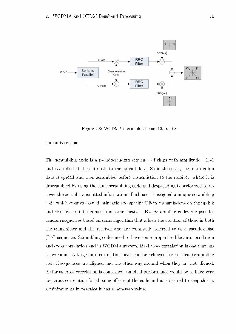
Serial to
ParallelChannelisation
CodeDPCH
I-Path
Q-Path
RRC
Filter
RRC
Filter
cos(ωt)
sin(ωt)
+1-1
+j
-j
1+j
1-j
-1+j
-1-j
Figure 2.3: WCDMA downlink scheme [10, p. 103]
transmission path.
The scrambling code is a pseudo-random sequence of chips with amplitude +1/-1
and is applied at the chip rate to the spread data. So in this case, the information
data is spread and then scrambled before transmission to the receiver, where it is
descrambled by using the same scrambling code and despreading is performed to re-
cover the actual transmitted information. Each user is assigned a unique scrambling
code which ensures easy identi�cation to speci�c UE in transmissions on the uplink
and also rejects interference from other active UEs. Scrambling codes are pseudo-
random sequences based on some algorithm that allows the creation of these in both
the transmitter and the receiver and are commonly referred to as a pseudo-noise
(PN) sequence. Scrambling codes need to have some properties like autocorrelation
and cross correlation and in WCDMA system, ideal cross correlation is one that has
a low value. A large auto correlation peak can be achieved for an ideal scrambling
code if sequences are aligned and the other way around when they are not aligned.
As far as cross correlation is concerned, an ideal performance would be to have very
low cross correlation for all time o�sets of the code and it is desired to keep this to
a minimum as in practice it has a non-zero value.

2. WCDMA and OFDM Baseband Processing 11
2.1.2 Modulation
The WCDMA downlink consists of Dedicated Physical CHannel (DPCH) which is
a stream of binary information. This binary information is converted into polar
format as de�ned in 3GPP speci�cations according to which the binary '0' maps
to a +1 polar signal and binary '1' maps to a -1 polar signal. After mapping, the
DPCH passes through a serial to parallel (S/P) converter which alternately passes
them to two streams termed as in-phase (I-plane) and quadrature plane (Q plane)
symbols. Based on the required data rate, both of these polar streams are spread
using the same channelization code. To remove the high frequency variations, data
from both planes are passed through RRC �lter followed by multiplication of I-plane
data with a cosine function and Q-plane data with a sine function. The Figure 2.3
shows the WCDMA downlink transmission phase and constellation where I-plane
takes the values of +1 and -1 and Q-plane takes the values of +j and -j represented
using complex arithmetic. The composite signal will take the values of 45, 135, -45
and -135 degrees and corresponds to the vector sum of I and Q. [10, p. 102-103]
In WCDMA uplink transmissions, there is a di�erence in the type of information the
I-plane and Q-plane carry as shown in Figure 2.4. I-plane carries DPDCH channel
which consists of user tra�c and control signaling and the spreading factor used
for it varies between 4 and 256 which corresponds to data rates between 960 kb/s
and 15 kb/s. On the other hand, the Q-plane carries DPCCH which carries pilot
bits, power control (TPC) bits, feedback mode indicator (FBI) bits and transport
format combination indicator (TFCI) bits. The DPCCH uses a spreading factor
of 256 which corresponds to physical channel data rate of 15 kb/s and uses the
channelization code of 0. The modulation used for uplink is similar to that used
for downlink and hence uses the same I and Q planes which are �ltered using RRC
�lter and then quadrature up-conversion procedure is applied. [10, p. 108-110]
2.1.3 Rake Receiver Concept
The rake receiver is considered as an e�cient implementation of a receiver used in
WCDMA based systems to recover the transmitted symbols. There are independent

2. WCDMA and OFDM Baseband Processing 12
physical channels used to transport data, control and pilot information which are
usually time-multiplexed in these physical channels. It is the responsibility of the re-
ceiver to de-multiplex the data and control information. The recovered data symbols
are forwarded to bit rate processing block for error detection and correction that
may have occurred during transmission while the control information is correctly
acted upon. The process of recovering the transmitted symbols is accomplished by
the rake receiver which has to execute di�erent signal processing algorithms. The
baseband functional blocks in this receiver includes multipath searcher, rake �ngers,
channel estimator and the maximal ratio combiner. By using these baseband blocks,
rake receiver performs the operation of synchronization, demodulation, channel es-
timation and channel equalization. A high level block diagram of a rake receiver is
shown in Fig 2.5. In the following subsections, we will discuss in su�cient length
about the baseband functions performed by these individual blocks of the rake re-
ceiver.
Timing Synchronization
When the user switches on the mobile terminal, the terminal starts searching for
the closest base station or cell so that the services provided by the core network
can be used. The user equipment searches for the nearby cell and gets the timing
information which includes slot timing, frame timing and the cell ID (identi�cation).
The operation performed to get all this information is called the cell search procedure
DPDCH
Cch,1 βd
DPCCH
Cch,0 βc
I-Path
Q-Path*j
Sdpch,n
RRC
Filter
RRC
Filter
cos(ωt)
sin(ωt)
Figure 2.4: WCDMA uplink scheme [10, p. 109]

2. WCDMA and OFDM Baseband Processing 13
PULSE SHAPE
FILTERING
MULTIPATH
SEARCHER
RAKE
FINGER #1
RAKE
FINGER #2
RAKE
FINGER #3
RAKE
FINGER #4
EXTRACT
PILOT
SYMBOLS
MAXIMAL
RATIO
COMBINER
CHANNEL
ESTIMATION
SYMBOL
MAPPING
Figure 2.5: Digital baseband section of WCDMA receiver c©IEEE, 2007 [11]
and is described in the next subsection.
Cell Search
The cell search is the algorithm performed by the user equipment to detect the pres-
ence of cells it has no information about. The user equipment follows a three-stage
procedure to �nd and then synchronize to a cell and is based on three fundamental
physical layer channels. These signaling channels are available in every cell and
referred to as Primary Synchronization Channel (P-SCH), Secondary Synchroniza-
tion Channel (S-SCH) and Primary Common Pilot Channel (P-CPICH). The three
stages of the cell search operation are slot synchronization, frame synchronization
and scrambling code identi�cation.
The objective of the slot synchronization stage is to detect the presence of cell and
to �nd the slot start time. For this purpose, P-SCH is used in which a known 256-
chip-long sequence is broadcasted at the beginning of every slot on downlink. The
receiver correlates the received signal with the locally stored P-SCH code sequences
to identify its presence. The series of pulses are found at the output of matched �lter
at the start of each slot and hence provides an indication of the slot boundaries. In
frame synchronization, the receiver uses the S-SCH channel to determine the frame
synchronization and scrambling code. The S-SCH uses 256-chip-long codeword for
each slot and at the start of each slot, a di�erent codeword is transmitted. The
order and the de�nition of these code words are very important as this is how the
2. WCDMA and OFDM Baseband Processing 14
UE identi�es the code sequence to �nd the frame timing and code group. In the
third stage, the identi�ed code group is used to �nd the exact primary scrambling
code used by the cell. The received signal is correlated with the eight di�erent
scrambling codes which belong to the identi�ed code group. The code resulting in
strongest correlation output is selected as the cell's primary scrambling code.
Multipath Propagation
In radio propagations, the signal transmitted from an antenna may su�er from re-
�ections and di�ractions due to obstacles like buildings in the coverage area. The
signal travels through multiple independent paths and hence at UE or Node B, it
arrives along with multiple re�ections. These multiple signals are called multipath
components and this phenomenon is generally referred to as multipath propagation.
The impact of these multipath components can be ignored in systems with small
bandwidth but the e�ects on system performance needs to be considered if the band-
width is higher. In narrow band communication system, an optimum receiver uses
correlation and integration methods and operates e�ciently in �at Rayleigh fading
situations. A single correlator can provide optimum performance in narrow band
systems but in multipath fading channel, it su�ers from problems. In multipath
propagation, additional correlators are used to overcome the inter-symbol interfer-
ence which can degrade performance and hence leads to a design of a complete rake
receiver.
In a typical spread spectrum receiver, a locally generated de-spreading waveform
is multiplied with the received signal on a sample by sample basis. The resulting
signal is then integrated over a period of transmitted symbol and �nally the output
is sampled. In multipath propagations, the despreading and descrambling sequence
is time-aligned with the received multipath component which corresponds to spe-
ci�c path and hence the time delay. The despreading signal has to be time-aligned
with one of the multipath components to despread it correctly. The signal arrival
time must be known and hence synchronized with the despreading and descrambling
waveform. Depending upon the number of correlators used, the timing arrangements

2. WCDMA and OFDM Baseband Processing 15
need to be made for the strongest multipath components. The outputs of the cor-
relators are then combined which leads to a better signal to noise ratio (SNR) than
the SNR of individual multipath components. To obtain net power gain, the signals
are added coherently and the noise is added non-coherently. The time di�erence
between the correlators ensures that we can add together the outputs and combine
them correctly.
Multipath Estimation
In multipath radio propagations, the User Equipment (UE) receives multiple copies
of the single transmitted pulse. These multiple components may a�ect the receiver
performance if not properly taken into account. Due to signal's high bandwidth,
the e�ect of multipath components cannot be ignored. Hence in WCDMA systems,
multiple rake �ngers are used where each �nger corresponds to a speci�c multipath
component according to its delay pro�le. The multipath searcher identi�es the
strongest signal components and allocate each of them with a rake �nger. Depending
upon the environment, the signal components travel through di�erent paths and
arrive at di�erent time instants to UE. In [10, p. 189], the reported highest path
delays can be 5µs in an urban environment and 20µs in hilly areas. To obtain
multipath diversity, the time di�erence of multipath components should be at least
0.26µs which is the duration of a single chip [8, p. 31]. In this case, the WCDMA
receiver can separate those multipath components and combine them coherently.
A known pilot sequence is matched with the received signal to perform multipath
estimation operation as shown in Eq. 2.1
y(k) =L−1∑l=0
t∗(l)r(k + l) (2.1)
where y(k) is the output of the matched �lter, t∗(l) is the complex conjugate of
pilot symbol and L is the length of the correlation [11]. The multipath estimation
process has been described as a two-stage process namely as acquisition and tracking
in [12]. In acquisition stage, the arrival of �rst signal component is detected and
in tracking stage, the changes in multipath taps are followed within a certain time
span. The amplitude of the correlation peak corresponds to the gain of the multipath
2. WCDMA and OFDM Baseband Processing 16
component and a path delay can be measured by using the time o�set relative to
the �rst peak arrival. The noise and interference caused from other users may a�ect
the system performance, hence the process of averaging the sequential estimation
windows non-coherently is used and is shown in Eq. 2.2
yave(k) =1
M
M−1∑m=0
|ym(k)|2 (2.2)
where ym(k) is the kth element of the mth correlation window [11]. In [13], it is
stated that the multipath searcher receives the pseudo-noise (PN) sequence from
Base Transceiver Station (BTS) as a result of cell search operation. The alignment
of this PN sequence corresponds to the strongest multipath and is used to �nd other
multipaths by correlating it with the P-CPICH symbols. The rake �ngers are then
con�gured accordingly based on the relative o�set of the multipath. The multipath
searcher operates continuously as it is highly likely that the UE changes its position
frequently.
Demodulation
In a narrow band receiver, a single correlator is generally used to recover the trans-
mitted symbols. A correlator multiplies the received signal with a copy of the
transmitted pulse and integrates the output after the multiplication process for the
duration of the symbol period. Once this operation completes, the integrator is
reset and decision can be made on the transmitted symbol. All this is quite opti-
mum when it comes to narrow band transmissions but it may su�er from problems
when bandwidth is higher due to multipath fading channel. In WCDMA systems,
the receiver has more than one correlator and is assigned to one of the multipath
components. The output of the ith rake �nger is shown in Eq. 2.3
di(n) =
Lsf−1∑l=0
c∗s(l + nLsf )r(l + τi + nLsf ) (2.3)
where cs represents the combined spreading and scrambling codes, Lsf is the spread-
ing factor and τi is the multipath estimate for the ith rake �nger [11]. The correlators
perform despreading and descrambling operations and �nally the outputs are com-

2. WCDMA and OFDM Baseband Processing 17
bined. As a consequence, a large bandwidth signal with low power spectral density
turns into a narrow-band signal with a higher power spectral density. The bene�t
of combining signals this way is the improved Signal-to-Noise Ratio (SNR) of the
resultant signal comparatively with the SNRs of individual components [10, p. 197].
The multipath components have some impact on the output of individual �ngers
but it can be minimized by using a large spreading factor.
Channel Estimation
To add the rake �ngers output coherently and synchronously, the channel's phase
and amplitude must be estimated for each of the identi�ed paths. The methods
generally used for this process includes data aided channel estimation, decision-
directed channel estimation and blind-channel estimation. Channel estimates can
be obtained either by using one or any combination of the above mentioned pro-
cedures. The sources available to perform this operation include Common PIlot
CHannel (CPICH) and the pilot symbols time-multiplexed within the slots of Ded-
icated Physical Control CHannel (DPCCH) [14]. The DPCCH is transmitted to-
gether with the DPDCH within each slot of the DPCH frame and consists of control
information bits like TFCI bits, the power control bits and of course the pilot bits.
The slot format of the downlink DPCH is shown in Fig 2.6. The symbols extracted
in demodulation operation performed in rake �ngers can be expressed as
di(n) = αid(n) + w(n) (2.4)
In Eq. 2.4, d(n) is the transmitted symbol, αi is complex attenuation of the ith
multipath, di(n) is the output of the rake �nger and w(n) is additive noise [11].
The channel estimate of the ith multipath can be computed when the transmitted
symbol is known and is expressed as
αi 'di(n)
d(n)(2.5)
Based on the chosen slot format, time-multiplexed pilot symbols of DPCCH are
demultiplexed from the received symbols and then correlated with the known pilot
2. WCDMA and OFDM Baseband Processing 18
symbol sequence. For improved performance, preliminary channel estimates are
used to make symbol decisions and then these symbols are used as pilot symbols
for the next stage to get more accurate estimates. As far as CPICH is concerned,
there is at least one such channel available in every cell and uses a �xed primary
scrambling code, hence named as Primary Common PIlot CHannel (P-CPICH). It
uses the spreading factor of 256 and does not carry any higher layer information.
[8, p. 103]
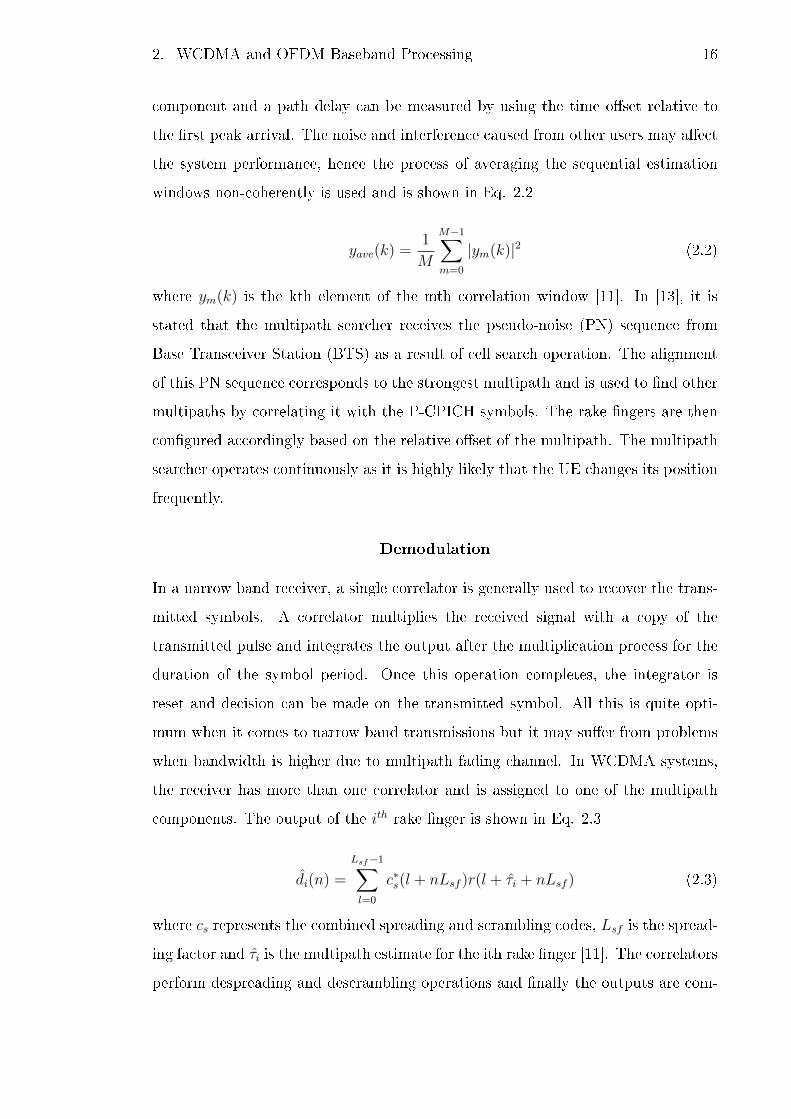
DATA1 TPC TFCI DATA2 Pilot
SLOT #0
10ms radio frame
2560 chips
NDATA1 bits NTPC bits NTFCI bits NDATA2 bits NPILOT bits
DPDCH DPDCHDPCCH DPCCH
SLOT #1 SLOT #2 SLOT #3 SLOT #14
Figure 2.6: Frame Structure for the downlink DPCH [9, p. 79]
2.2 OFDM Baseband Processing
Orthogonal Frequency Division Multiplexing (OFDM) is considered as a promising
solution for wired and wireless communication standards to achieve higher data rates
and immunity to issues like multipath fading and inter-symbol interference (ISI).
Instead of a single carrier system, OFDM uses multi-carrier modulation (MCM)
scheme in which multiple carrier frequencies are used to modulate parallel data
streams and hence transmitting the data in parallel over the communication chan-
nel. These carrier frequencies are orthogonal to each other and contain low rate data
due to lower bandwidth of individual channels. Digital audio broadcast (DAB), dig-
ital video broadcast (DVB), asymmetrical digital subscriber line (ADSL) Discrete
Multi-Tone (DMT), wireless LAN standards and now the LTE mobile communi-
cations are the popular applications area of this tremendous technology [15]. A
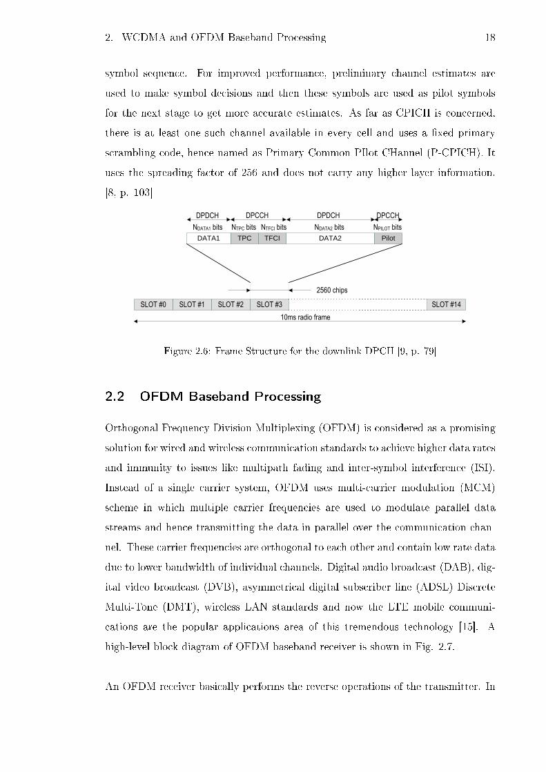
high-level block diagram of OFDM baseband receiver is shown in Fig. 2.7.
An OFDM receiver basically performs the reverse operations of the transmitter. In

2. WCDMA and OFDM Baseband Processing 19
the beginning, it estimates the frequency o�set and symbol timing by using the
special training symbols in the preamble. FFT operation is then performed to every
OFDM symbol to recover the 52-QPSK values of all subcarriers. The reference phase
and amplitude of the constellation on each subcarrier is required to estimate the bits
at receiver end. Correction for the channel response as well as remaining phase drift
can be made using the training symbols and pilot subcarriers. The recovered symbols
can then be demapped into binary values after which a Viterbi decoder can decode
the information bits. Every OFDM packet contains a preamble which is essential to
perform start-of-packet detection, automatic gain control, symbol timing, frequency
estimation and channel estimation. A guard interval is inserted at the end of each
OFDM symbol to eliminate the intersymbol interference almost completely. Also
the guard interval is chosen larger than the expected delay spread such that the
multipath components from one symbol cannot intefere with the symbol that follow.
2.2.1 IEEE 802.11a WLAN Overview
IEEE 802.11a is one of the approved WLAN standards which uses OFDM system
and hence transmits and receives information using several sub-carriers simultane-
ously. Inverse Fast Fourier Transform (IFFT) and Fast Fourier Transform (FFT)
are used for transmitting and receiving those sub-carriers respectively. The standard
uses a 5 GHz Unlicensed National Information Infrastructure (U-NII) band and has
the capability of transmitting at the maximum data rate of 54Mbps. In 802.11a
Pulse Shape
FilteringS/P FFT
Extract
Pilot
Symbols
Channel
Equalization
Symbol
MappingP/S
Timing EstimationChannel
Estimation
Figure 2.7: OFDM baseband functional block diagram c©IEEE, 2007 [11]

2. WCDMA and OFDM Baseband Processing 20
standard, the other supported data rates are 6, 9, 12, 18, 24, 36, and 48 Mbps and
it is mandatory to transmit/receive at 6, 12 and 24 Mbps. The system has a band-
width of 20MHz which splits into 64 carrier frequencies resulting in a sub-carrier
frequency spacing of 0.3125 MHz. From these 64 sub-carriers, 48 sub-carriers are
used to transmit the user data and 4 of them are used for pilot reference signals
whereas the remaining 12 subacrriers are not used. The modulation schemes used
are Binary Phase Shift Keying (BPSK), Quadrature Phase Shift Keying (QPSK),
16 Quadrature Amplitude Modulation (QAM) and 64 QAM. Channel coding can be
incorporated to achieve the same data rate but with improved BER performance. In
wireless systems, Convolutional codes have been the most widely used channel codes
for the last decades.[16, p. 36-38] Table 2.2 describes the physical layer speci�cations
of the IEEE 802.11a WLAN standard.
Table 2.2: Rate-dependent parameters of 802.11a c©IEEE, 1999 [17]
Data rate(Mbps)
Modulation Coding rate(R)
Coded bitsper subcar-rier (NBPSC)
Codedbits perOFDMsymbol(NCBPS)
Databits perOFDMsymbol(NDBPS)
6 BPSK 1/2 1 48 249 BPSK 3/4 1 48 3612 QPSK 1/2 2 96 4818 QPSK 3/4 2 96 7224 16-QAM 1/2 4 192 9636 16-QAM 3/4 4 192 14448 64-QAM 2/3 6 288 19254 64-QAM 3/4 6 288 216
2.2.2 MAC Frame Structure for IEEE 802.11a
The IEEE 802.11a standard uses a Carrier Sense Multiple Access with Collision
Avoidance (CSMA/CA) protocol for its Medium Access Control (MAC) layer and
uses Clear Channel Assessment (CCA) scheme to check the availability of the
medium. Also the sender expects an acknowledgement from the receiver as colli-
sions or fading may occur which may corrupt the data. Physical Layer Convergence

2. WCDMA and OFDM Baseband Processing 21
Protocol (PLCP) and Physical Medium Dependent (PMD) are the two sub-layers
of the 802.11a PHY layer where PLCP interacts with the MAC for the exchange
of information. Figure 2.8 shows the complete frame format of the IEEE 802.11a
WLAN standard.
RATE
4 bits
Reserved
1 bit
LENGTH
12 bits
Parity
1 bit
Tail
6 bits
SERVICE
16 bitsPSDU
Tail
6 bitsPad Bits
PLCP Header
PLCP Preamble
12 Symbols
SIGNAL
One OFDM Symbol
DATA
Variable Number of OFDM Symbols
Coded/OFDM
(BPSK, r = 1/2)
Coded/OFDM
(RATE is indicated in SIGNAL)
Figure 2.8: PLCP Protocol Data Unit (PPDU) frame format c©IEEE, 1999 [17]
The PPDU frame consists of PLCP preamble, header and the data �eld. The PLCP
preamble consists of 10 short training symbols and 2 long training symbols as shown
in Figure 2.9 and used for packet detection and symbol timing information.
t1 t2 t3 t4 t5 t6 t7 t8 t9 t10
10 x 0.8 = 8µs
Signal Detect,
AGC, Diversity
Selection
Coarse Freq.
Offset Estimation
Timing Synchronize
GI T1 T2
Channel and Fine Frequency
Offset Estimation
2 x 0.8 + 2 x 3.2 = 8.0µs
8 + 8 = 16 µs
Figure 2.9: PLCP preamble c©IEEE, 1999 [17]
In Figure 2.9, the ten short training symbols are from t1 to t10 and the two long
training symbols are T1 and T2. Both the short and long training symbol sequences
are of 8µs duration with the total time of 16µs. The sequence S shown in eq. 2.6 is
used to modulate the 12 subcarriers out of 52 by each of the short training symbols.

2. WCDMA and OFDM Baseband Processing 22
S−26,26 =√
(13/6)× {0, 0, 1 + j, 0, 0, 0,−1− j, 0, 0, 0, 1 + j, 0, 0, 0,−1− j, 0, 0, 0,
− 1− j, 0, 0, 0, 1 + j, 0, 0, 0, 0, 0, 0, 0,−1− j, 0, 0, 0,−1− j, 0, 0, 0, 1 + j,
0, 0, 0, 1 + j, 0, 0, 0, 1 + j, 0, 0, 0, 1 + j, 0, 0} (2.6)
There is an another sequence L which modulates 53 subcarriers for each of the long
training symbols and is shown in eq. 2.7. There is a Guard Interval (GI) between
the short and long training symbols to avoid inter-symbol interference. The duration
of this guard interval is 1.6µs
L−26,26 ={1, 1,−1,−1, 1, 1,−1, 1,−1, 1, 1, 1, 1, 1, 1,−1,−1, 1, 1,−1, 1,−1, 1, 1, 1, 1,
0, 1,−1,−1, 1, 1,−1, 1,−1, 1,−1,−1,−1,−1,−1, 1, 1,−1,−1, 1,−1, 1,−1,
1, 1, 1, 1} (2.7)
Hence, these short and long repetitions of known sequences are collectively termed
as preamble which is used for synchronization purpose. After the preamble part,
there is another �eld called SIGNAL �eld which is encoded using BPSK modulation
of the subcarriers. There is only one symbol in this SIGNAL �eld which consists
of 24 bits which are not scrambled. The type of information conveyed by this �eld
includes the RATE and the LENGTH of the TXVECTOR as shown in Figure 2.10.
The �rst four bits are reserved for RATE which represents the type of modulation
and the coding rate which is convolutional coding at R = 1/2. The bits from 5-16
represent the LENGTH �eld and bit 4 is reserved for future use. The supported data
rates mentioned in section 2.2.1 can be selected by using the speci�c bit patterns
already assigned for them in the standard. The LENGTH �eld is an unsigned 12-bit
integer and indicates the number of octets in the PSDU need to be transferred as
requested by the MAC layer. There is a parity bit P which is a positive (even) parity
for the bits 0-16. The last �eld is called the TAIL �eld which is 6 bits long and all
of them are set to zero as can be seen in �gure 2.10. After the SIGNAL �eld, the

2. WCDMA and OFDM Baseband Processing 23
0R1 R2
1 2R3 R4
3 4R
5 6 7 8 9
LSB
10 11 12 13 14 15 16 17 18 19 20 21 22 23
MSB P
RATE
(4 bits)
LENGTH
(12 bits)
SIGNAL TAIL
(6 bits)
”0” ”0” ”0” ”0” ”0” ”0”
Transmit Order
t1 t2 t3 t4 t5 t6 t7 t8 t9 t10
10 x 0.8 = 8µs
Signal Detect,
AGC, Diversity
Selection
Coarse Freq.
Offset Estimation
Timing Synchronize
GI T1 T2
Channel and Fine Frequency
Offset Estimation
2 x 0.8 + 2 x 3.2 = 8.0µs
8 + 8 = 16 µs
GI SIGNAL
0.8 + 3.2 = 4µs
RATE
LENGTH
Figure 2.10: SIGNAL �eld bit assignment c©IEEE, 1999 [17]
DATA �eld starts as shown in �gure 2.11.
t1 t2 t3 t4 t5 t6 t7 t8 t9 t10
10 x 0.8 = 8µs
Signal Detect,
AGC, Diversity
Selection
Coarse Freq.
Offset Estimation
Timing Synchronize
GI T1 T2
Channel and Fine Frequency
Offset Estimation
2 x 0.8 + 2 x 3.2 = 8.0µs
8 + 8 = 16 µs
GI SIGNAL
0.8 + 3.2 = 4µs
RATE
LENGTH
GI Data 1
0.8 + 3.2 = 4µs
GI Data 2
0.8 + 3.2 = 4µs
SERVICE + DATA DATA
Figure 2.11: Complete OFDM frame format c©IEEE, 1999 [17]
The data bits are all scrambled and this DATA �eld contains the SERVICE �eld,
the PSDU, the TAIL bits and the PAD bits. The SERVICE �eld consists of 16 bits
where the bits 0-6 are used to synchronize the descrambler in the receiver and the
bits from 7-15 are all reserved for future use as shown in �gure 2.12.
The scrambler initialization bits as well as the remaining 9 reserved bits are all set
to zero. To return the convolutional encoder to the 'zero state', the 6 bits of the tail
�eld are set to zero. Finally the pad bits in the frame are used to keep the number
of data bits a multiple of NCBPS that is the number of coded bits per OFDM symbol
(48, 96, 192 or 288). Hence the length of the message is multiple of NDBPS that is
the number of data bits per OFDM symbol. Also the appended bits are set to zero
2. WCDMA and OFDM Baseband Processing 24
0 1 2 3 4 5 6 7 8 9 10 11 12 13 14 15
Scrambler Initialization Reserved SERVICE Bits
Transmit Order
”0” ”0” ”0” ”0” ”0” ”0” ”0” R R R R R R R R R
Figure 2.12: SERVICE �eld bit assignment c©IEEE, 1999 [17]
and are scrambled by using the remaining bits in the DATA �eld.
2.2.3 OFDM WLAN Baseband Algorithms
The digital baseband section of OFDM WLAN receiver executes baseband algo-
rithms so that the transmitted symbols can be extracted. The baseband section
generally performs synchronization, demodulation, channel estimation and equaliza-
tion operations. The following subsections will explain these operations in su�cient
length pertaining to OFDM WLAN receiver.
Time and Frequency O�set Estimation
In order to extract the transmitted data symbols accurately, the receiver has to
synchronize itself with the incoming packet so that it can perform desired opera-
tions on the correct set of samples which is generally referring to the same OFDM
symbol. The synchronization process includes packet detection and symbol timing
information which can be obtained using the packet's preamble part. The preamble
is composed of ten repeated short symbols and two repeated long symbols where
each short symbol consists of 16 samples and each long symbol consists of 64 sam-
ples. There is a guard interval between the short training symbols and long training
symbols and contains 32 samples taken from the end of LTS. According to the IEEE
802.11a standard, the �rst seven short symbols would be used for packet detection,
automatic gain control (AGC) and diversity selection for Multiple Input and Multi-
ple Output (MIMO) systems [17]. The remaining three short symbols should be used
for Coarse Frequency O�set (CFO) calculation and time synchronization. Channel

2. WCDMA and OFDM Baseband Processing 25
Estimation and Fine Frequency O�set (FFO) calculation can be made using LTS
and can also be used to re�ne the time synchronization estimates. Hence in every
new transmission, the transmitter adds this preamble and then appends the actual
data symbols.
It is critical for a typical wireless receiver to detect the presence of a packet transmis-
sion in a wireless channel where various complicating factors distort the signal prop-
erties. Regarding OFDM modulation, the orthogonality among subcarriers may get
a�ected due to o�set between transmitter and receiver subcarrier frequencies which
may cause signi�cant degradation in system performance. Therefore to maintain
the orthogonality among subcarrier frequencies, the transmitter and receiver must
be precisely synchronized and this requires accurate frequency o�set calculation at
the receiver. But the �rst task is to detect the presence of a packet by exploiting
the repeated pilot symbols and to estimate the start of the Fast Fourier Transform
(FFT) window. We can get reliable and accurate estimates using preamble based
synchronization scheme and this operation gets completed in about �rst one to two
starting symbols.
Packet Detection
In 802.11a WLAN standard, the short training symbols can be used for packet
detection as they are identical and repeated for 10 times in the beginning of every
data packet. The packet detection can be achieved using delay and correlate method
in which a received signal is correlated against a delayed version of itself. The delay
and correlate method will yield an output y(k) which is given by
y(k) =L−1∑l=0
r(k + l)r∗(k +D + l) (2.8)
Here r(k) is representing the signal received, ()∗ identi�es the complex conjugate
operation, distance between two consecutive symbols is represented by D and L
is the length of the correlation. The received signal power during the correlation
period can be used to normalize the correlation output y(k) as given by
2. WCDMA and OFDM Baseband Processing 26
p(k) =1
2
L−1∑l=0
|r(k + l)|2 + |r(k +D + l)|2 (2.9)
Here p(k) is representing the energy of the received signal which can be used to
compute the decision metric as given by
M(k) =|y(k)|2
(p(k))2(2.10)
The decision metric M(k) reaches its maximum value when two di�erent correlation
windows match exactly. The �rst crossing-point of this metric against a preset
threshold value gives indication of packet presence. Hence, the value of M(k) is
compared against a threshold value and detection can be observed if correlation
peak crosses it.[11]
Symbol Timing Estimation
The symbol timing information is needed to identify the symbol boundaries so that
the FFT operation can be performed on the correct set of samples. Once the packet
is detected, the receiver starts searching for symbol boundaries using the same delay
and correlate algorithm. In 802.11a standard, the receiver uses the long training
sequence for symbol timing estimation by exploiting the sequential repeated known
symbols. Matched �lter approach can also be applied as an alternative and the
output is then computed as
y(k) =L−1∑l=0
t∗(l)r(k + l) (2.11)
Here t(l) is representing the training symbol and the symbol timing estimate would
correspond to the index giving the maximum value of y(k) within an observation
window.
τ = argmaxk{|y(k)|2} (2.12)
The received signal is correlated against the long training sequence and the edge of
the �rst FFT window is computed by detecting the largest correlation peak. The

2. WCDMA and OFDM Baseband Processing 27
packet detection is taken into consideration as a beginning of the search window
whose length is determined by longest expected propagation delay.[11]
Frequency O�set Estimation
A phase di�erence is introduced as a consequence of frequency o�set between trans-
mitter and receiver subcarrier frequencies that may lead to intersymbol interference.
This o�set can be estimated by observing the phase di�erence between the two iden-
tical symbols which is also proportional to the separation between the two transmis-
sions. In 802.11a standard, the short training symbols can be used for this purpose
by using the same delay and correlate method. The frequency o�set estimate can
be expressed as
f◦ = −1
2πDTs6 y(τ) (2.13)
Here Ts is representing the sampling period and D is distance between two training
symbols measured in samples. y(τ) is the correlation output at index τ which gives
its maximum value of y(k) within the observation window.[11]
Demodulation
Once the receiver has packet and symbol timing information, the next step is to
recover the transmitted data bits. The WLAN OFDM demodulator performs 64-
point FFT operation to recover the transmitted subcarriers and hence makes decision
on transmitted bits. Depending upon the type of constellation used, the received
symbols are estimated using the maximum-likelihood decision followed by hard or
soft decisions to obtain the assigned bits to those estimated symbols. The advantage
of using FFT is the reduced number of multiply-accumulate operations rather using
DFT implementation using correlation. By using the DFT operation, the nth symbol
output of the ith subcarrier will be determined as
Di(n) =M−1∑m=0
r(m+ τ + n(Lfft + Lcp))WmiM , i = 0, · · · ,M − 1 (2.14)
2. WCDMA and OFDM Baseband Processing 28
Here M is representing the length of the transform, τ is symbol timing estimate,
length of the FFT window is represented by Lfft , Lcp is the length of the cyclic
pre�x and WM = e−2π/M .[11]
Channel Estimation
In WLAN OFDM systems, the training data transmitted on every subcarrier is
used to perform the channel estimation operation. The long training symbols in
the WLAN preamble are used to estimate the channel response. The quality of the
channel estimate can be improved by averaging the contents of two long training
symbols as they are identical. In WLAN systems, the channel conditions generally
do not change during a data packet and hence assumed to be a quasistationary
channel. Thus channel estimation in OFDM is made using pilot symbols available
in the preamble of a data packet and valid for the entire packet. Considering a non-
frequency selective channel, after demodulation the received kth symbol is denoted
as
y(k) = h(k)x(k) + n(k) (2.15)
Here h(k) is representing the complex channel coe�cient corresponding to the kth
symbol and n(k) is additive white gaussian noise. As the transmitted symbols are
known, the channel estimate can be computed as
h(k) ≈ y(k)
x(k)(2.16)
The channel estimates can be computed using Eq. 2.10 for all the subcarriers us-
ing the training symbols employed in the preamble of the packet. The e�ect of
noise can be mitigated by averaging the several identical transmitted symbols in the
preamble.[12]
Symbols Demapping
Having performed the operations of synchronization, demodulation and channel es-
timation, �nally it is time for the receiver to make decisions on the transmitted

2. WCDMA and OFDM Baseband Processing 29
symbols. Depending upon the type of modulation used, the decision boundaries
determine how received symbols are mapped to bits. Considering the case of QPSK
modulation, there are four constellation points which are 90 degrees apart from each
other on a constellation diagram with I and Q axes. The maximum-likelihood deci-
sion is the constellation point that is closest to the received symbol. The computed
raw data symbols need to be corrected by using the maximum-likelihood approach to
determine the actual constellation points. In both the WCDMA and OFDM base-
band receiver implementations, the transmitted data symbols will be determined
using the technique of maximum-likelihood in which a relative distance between
received symbols and one of the constellation points is calculated and compared.
30
3. PLATFORM ARCHITECTURE
The hardware platform used in this experimental work is a homogeneuos Multipro-
cessor System-on-Chip (MPSoC) platform called NineSilica. The platform consists
of 9 Computational Clusters (CC) which are interconnected through a hierarchi-
cal Network-on-Chip (NoC). Each of the CCs contains a 32-bit general purpose
Reduced Instruction Set Computing (RISC) processing core called COFFEE as a
main processing element (PE), data and code memories and an NI.[18] The com-
plete platform has been designed and developed in the Department of Electronics
and Communications Engineering, Tampere University of Technology. The follow-
ing subsections will explain the architecture of COFFEE RISC core, the CC and
the MPSoC platform in su�cient detail.
3.1 COFFEE RISC Core
In this section, an introduction to the core is provided and also the hardware pe-
ripherals available for application development purpose are described. The core
execution pipeline is also described in this section.
3.1.1 Introduction to the Core
COFFEE is an open source RISC processor core also known as load and store ma-
chine which has been designed and developed in Tampere University of Technology.
The hardware features of the processing core are as follows;
• Harvard architecture
• 6 pipeline stages
• Multiplication of 16-bit and 32-bit operands
• Full precision 64-bit multiplication result in 4 clock cycles

3. Platform Architecture 31
• Two Separate register banks for fast context switching
• SW-con�gurable through a memory-mapped register bank
• Super user mode for OS-like functionality
• Memory protection mechanism
• Built-in 12-input interrupt controller
• Two timers
• Coprocessor interface
Some of the common features of the core like registers, timers, operating modes
and interrupts/exceptions will be described in more detail in the sections that fol-
low. Figure 3.1 shows an interface diagram of the COFFEE processor. Supporting
separate interfaces for data and instruction memories o�er freedom to chose any of
the memory type as long as interface timing requirements are met. Large and slow
main memories can be interfaced directly because of multi-cycle access support and
number of cycles per access can also be con�gured. Sharing of data bus might also
be considered for simple systems having single system bus and no cache memory.
Up to four coprocessors can be connected to COFFEE RISC core whose interface is
much like memory interface. Dedicated instructions are provided to move data and
instructions to and from coprocessors. Coprocessor ID (identi�cation) is speci�ed
using 2 bits and a �eld of 5 bits to specify the register index constitutes a total of
7 bits addressing. An interrupt signal is also provided in the interface such that the
coprocessor can interrupt the core in case of an exception. Also the coprocessor can
be connected to di�erent clock domains which is considered as an important feature
of the coprocessor interface.[19]
Referring to the interface diagram of the COFFEE core shown in Figure 3.1, PCB
(Peripheral Control Block) is provided to communicate with peripheral devices
around the core. PCB_WR and PCB_RD signals can be asserted using the memory
space reserved for peripherals and hence directing the access to the PCB. COFFEE
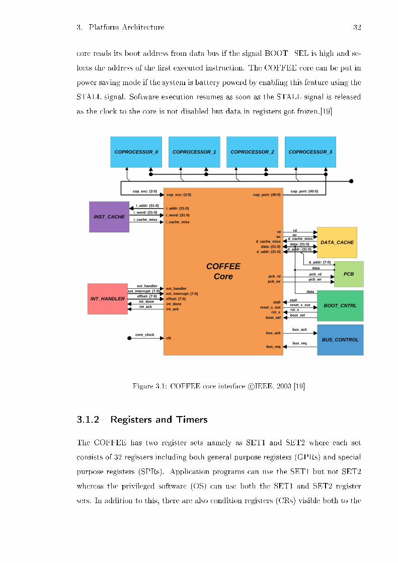
3. Platform Architecture 32
core reads its boot address from data bus if the signal BOOT_SEL is high and se-
lects the address of the �rst executed instruction. The COFFEE core can be put in
power saving mode if the system is battery powerd by enabling this feature using the
STALL signal. Software execution resumes as soon as the STALL signal is released
as the clock to the core is not disabled but data in registers got frozen.[19]
COPROCESSOR_0 COPROCESSOR_1 COPROCESSOR_2 COPROCESSOR_3
INST_CACHE
INT_HANDLER
DATA_CACHE
PCB
BOOT_CNTRL
BUS_CONTROL
COFFEE
Core
i_addr: (31:0)
i_word: (31:0)
i_cache_miss
i_addr: (31:0)
i_word: (31:0)
i_cache_miss
ext_handler
ext_interrupt: (7:0)
offset: (7:0)
int_done
int_ack
ext_handler
ext_interrupt: (7:0)
offset: (7:0)
int_done
int_ack
clkcore_clock
bus_ackbus_ack
bus_reqbus_req
stall
reset_x_out
rst_x
boot_selboot_sel
rst_x
stall
reset_x_out
pcb_rd
pcb_wrpcb_wr
pcb_rd
rd
wr
d_cache_miss
data: (31:0)
d_addr: (31:0)
rd
wrd_cache_miss
data: (31:0)
d_addr: (31:0)
data
d_addr: (7:0)
data
cop_exc: (3:0) cop_port: (40:0)cop_exc: (3:0) cop_port: (40:0)
Figure 3.1: COFFEE core interface c©IEEE, 2003 [19]
3.1.2 Registers and Timers
The COFFEE has two register sets namely as SET1 and SET2 where each set
consists of 32 registers including both general purpose registers (GPRs) and special
purpose registers (SPRs). Application programs can use the SET1 but not SET2
whereas the privileged software (OS) can use both the SET1 and SET2 register
sets. In addition to this, there are also condition registers (CRs) visible both to the

3. Platform Architecture 33
application programs as well as to the privileged software and they are 8 in total.
The condition registers are used in case of conditional branches or when instructions
are executed conditionally.
There is also an important register bank called Core Control Block (CCB) which is
memory mapped and contains both the control as well as the status registers used
in the processor operations. The advantage of being memory mapped is the access
to them using general load and store instructions and can be con�gured using boot
code. Most of the registers in these two sets are 32 bits wide with the exception of one
named as Processor Status Register which is 8 bits wide. The detailed description
of the Core Control Block registers like their addresses in memory, their usage and
bit �elds of the status register can be found in the user manual of the COFFEE
core.
As far as timers are concerned, COFFEE has two independent 32-bit timers that
can be con�gured to operate as a timer tick generator or as a watchdog timer. By
default, these timers use the same clock frequency as the core itself. Otherwise
there is an option called pre-scaling which can scale down the operating frequency
of these timers. The pre-scaling registers are 8 bits wide and can be accessed using
the same load and store instructions besides other registers like timer con�guration
register, register to hold maximum count and of course a free running timer register.
The timers can be enabled/run or stopped, continuous or go for once, generate an
interrupt on reaching a maximum count and also act as a watchdog timer to reset
the core in-case the core gets stuck somewhere. Again, refer to the user manual
for complete understanding of the timer registers and the options available for the
application developer.[20]
3.1.3 Operating Modes
Generally there are two modes of operation for the COFFEE core namely as super
user mode and user mode. In super user mode, the core can access the full memory
space along with both the register sets whereas in user mode, as stated earlier, only
�rst register bank is accessible. The user can switch from super user mode to user
mode but not vice versa unless a speci�c instruction is used which transfers the
3. Platform Architecture 34
execution to the system code. The core boots initially in the super user mode so as
to con�gure itself properly by accessing the core control block (CCB) registers and
then transfers control to the user mode.
There is a start-up sequence which needs to be followed while powering-up the
system like when the core powers up, the reset pin should be pulsed low to set the
core in the correct state. Also if the boot address selection is enabled, the data bus
should be provided with the boot address with the reset signal, otherwise it will boot
at address 0x00000000h. The core will boot in the super user mode (32 bits) where
interrupts are disabled and all the CCB con�guration registers are appropriately set
followed by transfer of control to the user mode.[20]
3.1.4 Interrupts and Exceptions
COFFEE core supports a total of 12 external interrupt sources where 4 of them
are reserved for coprocessors and the other 8 are for general purpose usage. In
addition to this, an external interrupt controller can be connected to further increase
the number of interrupt sources. The priorities for the coprocessor interrupts are
software programmable but for the external 8 sources, it is �xed. Priority can be set
by writing a 4-bit value in the corresponding �eld reserved for that source between
0 to 15, where 0 being the highest priority.
The interrupt is triggered by an interrupt signal and then it is serviced in the
following manner. The actions performed are priority resolving, switching to an
interrupt service routine and �nally returning from an interrupt service routine.
The interrupt handler registers are located in the Core Control Block (CCB) which
includes the control and the status registers. Similarly for an exception handling,
there are codes associated to those as well as the priorities of course.[20]
3.1.5 Core Pipeline Structure
COFFEE core consists of single pipeline with six stages where each stage performs
some operation or data transformation during one clock cycle. The intermediate or
�nal results are clocked to registers of successive stages and execution proceeds from
left to right. As there are six stages in the execution pipeline, it takes six clock cycles

3. Platform Architecture 35
FETCH
Instr.AddressCheck
Instr.Fetch
PCIncrement
DECODE
16 to 32 bitExtension
ImmediateOperandExtension
BranchAddress
Calculation
RegisterOperandFetch andForward
ExecutionCondition
Check
InstructionCheck
Status FlagEvaluation
EXECUTE
ALUExecution
Step 1
DataAddress
Calculation
EvaluationOf Flags
Z, N and C
MemoryOperandForward
CO-PROC
ALUExecution
Step 2
Co-ProcessorAccess
DataAddressChecks
DataForward
For MemoryAccess
ConditionRegister
Write
MEMORY
ALUExecution
Step 3
DataMemoryAccess
CCB Access
PCB Access
WriteBack
Figure 3.2: Core pipeline stages [21]
for an instruction to go through it. Ideally the throughput of the pipeline is one IPC
(Instructions Per Cycle) without any stalls which means that every clock cycle, a
new instruction enters the pipeline and one instruction completes its execution. The
core pipeline stages are shown in Figure 3.2 and brie�y described here as follows;
• Three operations are performed in the stage of FETCH. A new 32-bit instruc-
tion is fetched from the location pointed to by the program counter PC. A
32-bit double instruction is fetched if the address is even in 16-bit mode. An
address in PC is checked which may lead to exception generation in case of
violation. Depending upon the mode, program counter is �nally incremented
by two or four.
• From the control point of view, the DECODE stage is considered the most
important. Instructions are identi�ed and most of the decisions are made
about their behavior in the next stages. If the decoding mode is 16-bit, 16-

3. Platform Architecture 36
bit halfword is extended to an equivalent 32-bit instruction before passing
it to the decode logic. Special �elds inside instruction word which de�ne the
execution condition are evaluated. In evaluation, pre-evaluated condition �ags
against the speci�ed condition are checked. The instruction gets �ushed on
the next rising edge of the clock if execution condition is false. Signals required
during the current and following stages are decoded from the instruction word
simultaneously with the execution condition check. The control checks for
data dependencies based on signals evaluated in DECODE stage and signals
decoded from previous instructions currently on pipeline.
All data dependencies are resolved by forwarding the required data as soon
as it becomes available. FETCH and DECODE stages are put to STALL if
data cannot be forwarded and remain in this state until data becomes available.
Support of hardware to resolve dependencies makes programming and compiler
construction easier. The forwarding logic has approximately a delay of one-
third of a clock cycle which does not reduce the clock frequency but rather
improves the performance by avoiding unnecessary stalls.
Extending immediate operand, calculating PC relative jump address and eval-
uating new status �ags if needed are also other operations performed in DE-
CODE stage. At the end of the stage, the target address is clocked into the PC
register. In DECODE stage, all jump instructions and conditional branches
(PC relative and absolute) are executed. Register operands whether forwarded
or fetched from register �le are clocked to input registers of the EXECUTE
stage.
• Data is manipulated in the EXECUTE stage and integer addition, shift-
ing, boolean and bit-�eld manipulating instructions are completed during this
stage. All the multiplication operations started in this stage produce interme-
diate results to next stage. The ALU's adder is used to calculate the address
for data memory access. Condition �ags (Z = zero, N = negative, C = carry)
are evaluated at the end of the cycle using compare and some of the arithmetic
instructions.
3. Platform Architecture 37
• In the CO-PROC stage, instructions requiring more than one cycle continue
to be executed. Multiplication of 16-bit operands which produces a 32-bit
result �nishes in this stage. The condition �ags are written to selected condi-
tion register which were evaluated in the previous stage and are available for
DECODE stage prior written to condition register bank. How this is achieved
is by forwarding data inside condition register bank from input to output if
the source register and target register are the same. Also in this stage, the
data memory address calculated in previous stage gets checked along with ad-
dress comparison against memory limits set for user. Memory access is not
performed if the address points to the con�guration block, CCB, which is also
checked. All co-processors accesses are performed in this stage and address
calculation over�ow is detected too. Pipeline gets stalled during wait cycles
in case a co-processor access takes multiple cycles and hence performance de-
teriorates unless special interface block is used.
• 32-bit multiplication instructions execution completes in this stage of MEM-
ORY. Instructions like ld and st also complete their work during this stage
by accessing data memory. In case of multi-cycle execution, the rest of the
pipeline is stalled during wait cycles as MEMORY stage cannot be bypassed
by the instructions coming behind. Hence fast data memory or data cache and
prefetch capability are considered very important.
• Execution of all instructions gets completed in the last stage of Write Back
producing data which is written to the selected destination register. Internal
forwarding of register �le makes data in this stage visible to DECODE stage.
COFFEE is an RTL (Register Transfer Level) soft core described using VHDL and
can be ported to any technology with basic library components. The core was
designed to be a general purpose processing element suitable for most applications
in either SoC (System-on-Chip) environment or in more conventional embedded
systems. Its basic version provides adequate resources and processing power for
many applications but in various ways it can be enhanced. COFFEE core can be
customized as it was designed to be easily modi�able and provides simple interfaces

3. Platform Architecture 38
for expansion and communication. It is easy to instantiate COFFEE core anywhere
because of its simple interface. The main postulates for COFFEE core design were
reusability and con�gurability and it is published as an open source component.[19]
3.2 NineSilica MPSoC Platform
In this section, introduction to the homogeneous MPSoC platform is provided. The
functionality of computational cluster is introduced and other architectural mecha-
nisms are described.
3.2.1 Introduction to the Platform
NineSilica is a homogenous MPSoC platform derived from the Silicon cafe template
which allows creation of either homogeneous or heterogeneous architectures with an
unlimited number of computational nodes. This platform has been developed in the
Department of Electronics and Communications Engineering, Tampere University
of Technology. The platform contains nine computational clusters (CCs) connected
to each other in a mesh topology through a hierarchical Network-on-Chip. The tem-
plate does not de�ne the type of processing element (PE) inside the computational
cluster hence allowing creation of heterogeneous systems.
The nine computational clusters are organized in such a manner that there are three
computational clusters on each side of the square with the ninth one in the center
acting as the master on the NoC. The master CC is equipped with I/O peripherals
and it can access all the CCs using the well de�ned routing procedure. The master
CC's main responsibility is to manage the communication between slave CCs and
to control their activities. The Master CC manages the schedule by distributing
individual tasks to slave CCs to achieve parallelism and coordinates communication
with them. The central position of the Master CC is important in a sense that it
ensures a balanced latency across all slave CCs with maximum hop count of 2 in
between any slave and itself.[18] The NineSilica MPSoC platform is illustrated in
Figure 3.3.

3. Platform Architecture 39
Computationalcluster #0
NI
GS
Computationalcluster #1
NI
Computationalcluster #2
NI
GS GS
Computationalcluster #3
NI
GS
Computationalcluster #4(Master)
NI
Computationalcluster #5
NI
GS GS
Computationalcluster #6
NI
GS
Computationalcluster #7
NI
Computationalcluster #8
NI
GS GS
Off chip
I/O Interface
Figure 3.3: NineSilica MPSoC platform c©IEEE, 2009 [18]
3.2.2 Network-on-Chip (NoC)
Network-on-Chip as the name suggests is a communication network inside a single
chip and allows mostly PEs to be inter-connected. There is a local level of hierarchy
which provides non-blocking connections between processing core and its peripherals
forming a single node. The communication between nodes is enabled by a global level
of hierarchy via a mesh network. Based on the tra�c conditions, the interconnection
routes can be adapted at run-time. A lookup table with 16 possible routing paths
are available to each NI for the communication over the NoC. During a remote write
request from the local processor, 4 bits of the data address are used for the entry
value of the lookup table.[22]

3. Platform Architecture 40
3.2.3 Computational Cluster
The computational cluster is composed of COFFEE RISC core, scratchpad type
data and instruction memories (IMEM and DMEM) and a NI to latch together the
internal communication structure to NoC. Regarding the individual processing node,
a network interface is provided to each of the computational clusters (CCs) composed
of a bridge that allows the CC to write data using the NoC. The bridge is responsible
to latch together the global network communication with the communication inside
a computational cluster. In each CC, there are two contending initiators, one is
the processor itself and the other one is initiator side of the bridge (B/I). The idea
is that each CC has to use the global switch to interact with the rest of the CCs.
Processor can access the remote peripherals of another cluster by the local switches
to the target side of the bridge (B/I). The computational cluster is shown in Figure
3.4.
G
L
O
B
A
L
S
W
I
T
C
H
Initiator
NI
Target
NI
Local
Arbiter
Bridge
Network Interface
Request Switch
2:3
Response
Switch
3:2
Data
Memory
Code
Memory
COFFEE
RISC Core
Figure 3.4: Single computational cluster c©IEEE, 2009 [18]
The receiving computational cluster includes the target side of the bridge interface
(T-BIF), the local data memory and the local instruction memory of scratch pad
type. A run-time recon�gurable source routing table is used to pick up the route
to the destination address by T-BIF. Currently a total of 16 di�erent routes can be
con�gured and these routes are assigned to �xed size memory pages. This commu-

3. Platform Architecture 41
nication infrastructure supports both multicasting and broadcasting besides point
to point communication between the central node and any of the other slave nodes.
Each computational cluster hosts COFFEE RISC core as a PE due to its internal
architecture.
3.2.4 MPSoC Platform for SDR Applications
NineSilica is a homogeneous MPSoC platform in which the number of nodes are
kept at nine in order to limit the latency of data distribution and hence the commu-
nication overhead. Because of the mesh topology, it was decided to use nine nodes
where there is one control node and all the others are processing nodes. This is
how the intra-cluster data distribution requires only 1-2 hops and there is a uni-
form distribution of workload among the processing nodes. To execute remote read
and write operations, a distributed shared memory approach has been chosen where
each PE can write on a peripheral like data memory, instruction memory or net-
work interface. Direct read operation is not supported to avoid possible data races
due to remote read of an outdated variable. There is a shared space used for syn-
chronization and exchanges of addresses of remote variables. Read operations are
performed as write request to the remote cluster where the cluster updates the value
in the shared variable. Also the data coherence is maintained at application level
by the application developer as COFFEE RISC core is cacheless. Communication
protocols like shared memory and message passing can be implemented e�ciently
on this platform.
Regarding the performance of the platform if we consider the applications mapping,
the speedup close to the theoretical limits of N (number of nodes) can be achieved.
All this is made possible because of the scalability which has often been attributed to
the broadcast and multicast support of the hierarchical NoC. From the application
developer's view point, the platform is programmable in C language and every node
has its own instruction memory from where the local PE executes the program
instructions. Generally a couple of C code �les are prepared, one for the master core
and the other one for all the processing cores. There is no need to write N code �les
for each of the available processing nodes due to logical division of the platform into

3. Platform Architecture 42
control node and processing node. Each processing node is identi�ed by a unique ID
which is assigned at run-time by the control node hence processing nodes application
partitioning can be parameterized according to their IDs. The software written for
the control node is mostly responsible to initialize the platform and maintaining the
synchronization among the cores while executing the application software. Based
on the assigned IDs, individual processing nodes identify their responsibilities along
with the data set to operate on, number of data exchanges to be made and status
and control �ags communications.[22]
3.2.5 Communication and Synchronization
For real world communications, the control node is provided with I/O interfaces.
Considering baseband signal processing applications, the control node receives data
from outside world and distributes them to processing nodes for further computa-
tions. For inter-node communications, 32-bits are reserved to route the data packet
to the intended peripheral like DMEM, IMEM or NI. Control node assigns IDs to
individual processing nodes followed by sharing of synchronization signals as a part
of initialization of the platform. The processing nodes follow instructions from con-
trol node before starting any process either computation or communications. Once
the required data is made available to all the processing nodes, control node then
sends them a control signal to initiate the computation process. Upon completion
of the assigned task, each of the processing nodes asserts the status signals such
that the control node can proceed for further actions. Finally the processing nodes
are asked to transfer the computed results back to the control node. Based on this
�ow of execution, the control node of the platform acts as tasks scheduler and con-
trols the task distribution among the processing nodes. Addressing schemes like
point-to-point communications, multicasting and broadcasting are also supported
in this architecture. If data is to be transferred to all the processing nodes, using
broadcasting mode of communications can save almost 30% of the time.[22]

3. Platform Architecture 43
Table 3.1: Stratix II synthesis results of NineSilica MPSoC c©IEEE, 2009 [18]
Component Adapt. LUT Registers Utilization %COFFEE RISC 7,862 4,945 7.5
Local network node 346 232 0.3Computational node 8,237 5,177 8
Global network 2,813 3,548 3Total 76,780 50,482 73
Table 3.2: Stratix IV synthesis results of NineSilica MPSoC c©IEEE, 2010 [23]
Component Adapt. LUT Registers Utilization %COFFEE RISC 7,054 4,941 2.0
Local network node 296 226 0.1Computational node 7,360 5,167 2.1
Global network 5,104 4,170 1.3Total 71,679 50,897 20
3.2.6 Hardware Implementation
The synthesis results of this MPSoC platform on an Altera Stratix II FPGA device
(EP2S180) as well as on Altera Stratix IV FPGA device (EP4SGX530) are reported
in [18][23]. The operating frequency in fast mode is reported as 180MHz whereas in
the case of Stratix II device, the maximum operating frequency reported is 75MHz.
The synthesis of the platform has been made using the Quartus II version 8.0 SP1
design �ow. If we compare the synthesis results of Table 3.1 and Table 3.2, the
amount of resources occupied is roughly the same for both the cases but as far
as hardware resources are concerned, the design on Stratix IV device utilized only
20% of the available resources as it is a larger platform. The architecture runs at a
frequency of 115MHz in the FPGA slow mode.
NineSilica is a �exible and scalable platform which provides instantiated tiles of the
same nature for mapping varying nature of applications. By carefully identifying the
requirements, inherent parallelism can be exploited to achieve better performance
outcomes. Maximum performance can be obtained by minimizing the unnecessary
overhead and by proper planning of task distribution.

44
4. ALGORITHMS MAPPING
A typical baseband receiver executes digital signal processing algorithms to extract
the bit stream transmitted from source equipment. To test the functionality of the
baseband algorithms, a random sequence of symbols are generated using selected
constellation and performed the necessary physical layer procedures according to
3GPP (FDD) and IEEE 802.11a speci�cations. Pulse shape �ltering is applied to
the generated signal and then distorted by using simple channel model which adds
multipath taps and average white gaussian noise to the signal. The signal is then
�ltered again with the receiver version of the pulse shape �lter and saved in an array
that serves as an input to the receiver. All these operations have been performed
using MATLAB software to generate the input test stream for the receiver such that
it can perform the baseband operations.
4.1 WCDMA Parameters
The constellation used for this experimental work is QPSK and the Signal-to-Noise
(SNR) ratio of 25dB. The transmission slots for WCDMA is 15 within a single frame
of 10ms duration. The chip rate is 3.84MHz and the maximum length of the channel
delay spread is 1024. The relative delays of multipath components are also set with
the corresponding number of rake �ngers which is 4. The Spreading Factor (SF)
is 32 and the Pseudo-random (PN) sequence is generated using scrambling code
number of 512. The Dedicated Physical CHannel (DPCH) is formed using Dedi-
cated Physical Data CHannel (DPDCH) and Dedicated Physical Control CHannel
(DPCCH). Control and data information are multiplexed on each one of the DPCH
slots forming a complete frame of 10ms duration. The control information includes
Transmit Power Control (TPC), Transport Format Control Indicator (TFCI) and
PILOT symbols altogether form a DPCCH channel. The DPDCH consists of data
symbols transmitted within each slot of DPCH de�ned as DATA1 and DATA2 �elds

4. Algorithms Mapping 45
as shown in Fig 2.6. The DATA1 �eld consists of 14 symbols, DATA2 of 56 symbols,
TPC of 2 symbols, TFCI of 4 symbols and PILOT consists of 4 symbols altogether
result in 80 symbols. Hence a complete frame of DPCH composed of 1200 symbols
�nally gets modulated by performing the operations of spreading and scrambling.
Common PIlot CHannel (CPICH) is also used such that the receiver can perform
the operation of multipath estimation. CPICH is also spread using a SF of 256 and
scrambled using the same PN sequence.
4.2 WCDMA Baseband Processing
The WCDMA receiver baseband signal processing involves multipath estimation, de-
modulation, channel estimation and symbols demapping algorithms execution. The
software implementation of WCDMA baseband algoritms for NineSilica platform
are described here as follow;
4.2.1 Multipath Estimation
The multipath estimation kernel has been implemented in a way that in the begin-
ning it detects the �rst multipath peak. In order to perform this operation, CPICH
is used as a reference pilot sequence. CPICH is spread using a spreading factor
of 256 and scrambled using a PN sequence. The PN sequence has been generated
by using M-sequences with the scrambling code number of 512. The NineSilica's
control node transfers this received sequence of pilot symbols to all the processing
nodes. The DPCH is spread using a spreading factor of 32 and scrambled using the
same PN sequence. These data symbols are also transferred to processing nodes
after the coe�cients. Once every processing node has got these sequences, they
start performing correlation operations. After the completion of correlation opera-
tions, each of the processing nodes return the computed outputs to the control node.
The control node then starts searching for the correlation peak by comparing the
correlation outputs with the preset threshold value. When the control node �nds
a correlation peak, it broadcasts its index value corresponding to the �rst peak to
all the processing nodes. The processing nodes then start to compute more corre-
lation operations inside the tracking window. The sliding correlation operation is

4. Algorithms Mapping 46
performed between the received data and the known pilot sequence using the �rst
peak index as a starting point. The correlation output is averaged over a number of
slots and again these results are transferred to control node. The control node then
�nds the other three correlation peaks from the averaged correlation outputs as we
have a total of four rake �ngers in the receiver.
4.2.2 WCDMA Demodulation
Once the receiver has information about multipath components, the rake �ngers
can be con�gured according to their delay pro�les. The detected multipath compo-
nents de�ne the starting times of four di�erent received data sequences. The locally
generated despreading signal needs to be synchronized for each of the detected mul-
tipath components. The demodulation operation is performed by despreading and
descrambling the multipath components using the time-aligned despreading wave-
form. The spreading factor we have chosen for this experimental work is 32, which
corresponds to 80 symbols trasmitted per slot. As there are 15 slots in each WCDMA
frame, so in total we have 1200 symbols per frame. There are four rake �ngers in
the rake receiver, hence each of the processing nodes correlates 150 symbols for each
one of the rake �ngers. The starting index value for correlation corresponds to the
multipath component detected in multipath estimation. Each processing node de-
spreads and descrambles 600 symbols in total and thus the eight cores perform these
operations on 4800 symbols.
4.2.3 Channel Estimation
Channel estimation has been performed using the time-multiplexed DPCCH chan-
nel pilot symbols. As stated already in the previous paragraph that there are 80
symbols transmitted per slot. From these 80 symbols, 70 symbols are reserved for
user data and other 10 symbols are used for control information. From these 10
symbols, 4 symbols per slot are used as pilot symbols. The received pilot symbols
need to be extracted from the output of each rake �nger. These recovered pilot
symbols are correlated with the known pilot symbol sequence for each slot. Hence
the preliminary channel estimates can be computed for the slot in question. The

4. Algorithms Mapping 47
individual contribution of signal components are combined such that the SNR of
resultant signal is maximized. The extracted symbols from the rake �ngers are then
combined and scaled with estimated phase and magnitude of the propagation path.
Finally, the data symbols are extracted from these combined symbols. The NineSil-
ica's control node transfers the demodulated data to all the processing nodes. Each
of the processing nodes processes 160 symbols except the last node which processes
80 symbols. Because of �fteen slots in a frame, each processing node operates on
a couple of slots but the last node operates on the �fteenth slot and that is how
channel estimates are computed and data symbols are extracted.
4.3 OFDM Parameters
The constellation type chosen to generate the OFDM symbols is QPSK with the
SNR of 25dB. Number of OFDM symbols used in the simulation are 15 and a simple
Additive White Gauusian Noise (AWGN) channel is used. The length of an OFDM
symbol is 4µs which is composed of a signal part as well as a cyclic pre�x part.
The signal part is of 3.2µs duration whereas the pre�x part is of 0.8µs duration.
The number of data symbols within a single OFDM symbol is 48 and there are 16
cyclic pre�x symbols which altogether result in 64 symbols. The signal's bandwidth
of 20MHz is divided into subcarriers with spacing of 312.5KHz which yield in 64
subcarrier frequencies of which 52 subcarrier frequencies are used for modulation.
Four of the subcarrier frequencies are used for pilot symbols and the zero frequency
signal is not used. To generate the OFDM WLAN packet, training sequences are
generated for packet's preamble as per IEEE 802.11a standard. Having generated
the short and long training sequences for the packet preamble, the random data
symbols are generated for each of the OFDM symbols. As there are 15 OFDM data
symbols speci�ed for this experimental work, each of the OFDM symbols consists
of 48 data symbols which results in 720 data symbols for the entire OFDM packet.
Finally the signal is modulated using Inverse Fast Fourier Transform (IFFT) and
then the cyclic pre�x is added to each of the OFDM symbols to compose a complete
OFDM packet.

4. Algorithms Mapping 48
4.4 OFDM Baseband Algorithms Mapping
The OFDM baseband receiver pertaining to IEEE 802.11aWLAN standard performs
the operations of symbol timing and frequency o�set estimation, demodulation,
channel estimation and symbols demapping. The software implementation of OFDM
baseband algorithms for NineSilica platform are described here as follow;
Timing Synchronization
Due to high data rate and packet switched nature of WLAN systems, a "single-
shot" synchronization procedure is used in which synchronization is acquired very
quickly once the packet starts. There is a preamble in the start of every packet as
shown in Figure 2.8 which facilitates the single-shot synchronization. The start of
the packet is unknown to the receiver due to random access network, therefore the
�rst task is to detect the start of the incoming packet. Hence, the main tasks which
are performed in the beginning includes the packet synchronization and the symbol
synchronization.
The �rst synchronization algorithm executed is the packet synchronization in which
an approximate estimate of the incoming data packet is found. Several approaches
to packet detection exist like received signal energy detection, double sliding window
packet detection and using the structure of the preamble. I have used the preamble
structure for packet synchronization and hence will explain it brie�y here. Referring
to Figure 2.9, there are 10 identical short training symbols where each one of them
is 16 samples long followed by two identical long training symbols where each one
is 64 samples long. To exploit the periodicity of the short training symbols at the
start of the preamble, a delay and correlate algorithm is used. A crosscorrelation
operation is performed between the received signal and a delayed version of itself
where the delay z−D is equal to the period of the short training symbols that is D
= 16. The received signal energy is calculated to normalize the decision statistic
during the crosscorrelation window.
Once the packet timing is known to the receiver, it starts �nding the symbol timing

4. Algorithms Mapping 49
such that the Discrete Fourier Transform (DFT) of individual OFDM symbols can
be calculated. The result of DFT is then used to demodulate the subcarriers of
the individual symbols. To obtain symbol timing information, the receiver again
uses the known preamble and performs the crosscorrelation operation. The received
signal is crosscorrelated with the known reference like the end of the short training
symbols or the start of the long training symbols.
4.4.1 OFDM Demodulation
To demodulate the subcarriers at the receiver, the reverse operation of Inverse Fast
Fourier Tranform (IFFT) is used which is referred to as Fast Fourier Transform
(FFT). The output of the FFT contains Ns QPSK values which are then mapped
onto binary values and decoded to produce binary output data. The computation of
N-point FFT using the algorithms of radix-2, radix-4 and radix-8 has been presented
in [24]. The performance evaluation has been made using the number of clock cycles
comsumed and based on the given results, radix-2 has been declared best in terms
of speed-up achieved and parallelization e�ciency. But when it comes to required
clock cycles, radix-4 algorithm gives the best improvement for both the 64-point and
2048-point FFTs. In this research work, the hardware platform used to evaluate the
performance of these FFT algorithms is NineSilica. The main processing element is
COFFEE RISC core and the performance comparison between single-core and multi-
core platforms is also provided. Regarding the OFDM WLAN demodulation, 64-
point FFT operation is performed to recover the transmitted subcarrier frequencies.
The implementation details along with the pro�ling results are very well explained
in the given reference paper in this subsection.
4.4.2 Channel Estimation and Equalization
The channel estimation operation is performed using the long training sequence as
the transmitted sequence is already known to the receiver. Before computing the
channel estimation coe�cients, the two identical training symbols are averaged. In
the beginning, the pilots on the data subcarriers are extracted from the training
sequence which are referred to as reference pilot symbols. All the processing nodes

4. Algorithms Mapping 50
perform this operation and extract equal share of pilot symbols from the total of 48.
In this case, each processing node has 6 pilot symbols extracted from the reference
long training sequence. After that, the received pilots on the data subcarriers are
extracted and averaged. As there are two identical long training symbols transmit-
ted which correspond to 96 pilot symbols in total. Each processing node extracts 12
samples from both the long training symbols where 6 of them are from each symbol
and averages them. Now the processing nodes have both the reference pilot symbols
as well as the received pilot symbols. Each processing node starts computing the
channel estimates by taking the ratio of the reference pilot symbols to the received
pilot symbols. After computing the channel esitmates, each processing node trans-
fers the results back to the control node.
The demodulated data symbols are equalized using the equalization coe�cients ob-
tained for each of the subcarriers. As there are 15 data symbols used for this
experimental work and in each data symbol, there are 48 data samples modulated,
therefore these 48 data samples for each of the data symbols need to be equalized
using the computed channel estimates. In the beginning, the control node transfers
the channel estimates to all the processing nodes followed by transferring the re-
ceived data symbols. Each one of the processing node has been transferred a couple
of data symbols except the last node which was provided with only one data sym-
bol. Therefore each processing node equalizes 96 data samples except the last node
which equalizes 48 data samples.
4.5 Symbols Demapping
To make decisions on the transmitted symbols for both the cases of WCDMA and
OFDM baseband receivers, the decision boundaries determine how received sym-
bols are mapped to bits. The maximum-likelihood decision is the constellation
point that is closest to the received symbol. The computed raw data symbols need
to be corrected by using the maximum-likelihood approach to determine the actual
constellation points. In both the WCDMA and OFDM baseband receiver imple-
mentations, the transmitted data symbols are determined using the technique of
4. Algorithms Mapping 51
maximum-likelihood in which a relative distance between received symbols and one
of the constellation points is calculated. The constellation point corresponds to the
minimum distance was selected as a transmitted symbol.
Once the data symbols are extracted, each of the processing nodes starts making de-
cisions on the recovered data symbols. The extracted symbols need to be demapped
according to the constellation type used at the transmitting end. Quadrature Phase-
Shift Keying (QPSK) modulation scheme has been used so there are four constella-
tion points. The processing nodes �nd the transmitted symbols by computing the
absolute distance between the recovered symbol and those four constellation points.
For the case of WCDMA baseband receiver, each of the processing nodes demap
140 data symbols except the last node which processes 70 symbols. Finally, the
demapped symbols are transferred to the central control node for further processing.
For the case of OFDM baseband receiver, after performing the operation of equaliza-
tion, the processing nodes already have the data samples which can be demapped.
All the nodes have 96 data samples except the last one which has 48 data samples.
All the processing nodes perform the same operation on the recovered data samples
and �nd out the actual transmitted contellation points. Once all the nodes are done
with this process, they transfer back the �nal results to the control node. The pro-
cessing nodes also determine the number of corrupted data samples by comparing
the recovered data samples with the actual transmitted data samples. Finally the
control node �nds out the total number of erroneous samples as well as the Bit Error
Rate (BER).

52
5. RESULTS
The algorithms have been implemented using C language with 16-bit �xed-point
arithmetic. The results have been compared with the MATLAB model and func-
tional correctness has been veri�ed. For simulations purpose, the Mentor Graphics
ModelSim simulator has been used. In the beginning, the algorithms have been
mapped on the single core of COFFEE processor followed by implementation on
NineSilica platform. The idea behind this experimental work was to exploit the
parallelism o�ered by multicore systems and to evaluate the performance di�erence
between single core and multicore platforms. Table 5.1 shows the pro�ling results
of the WCDMA baseband algorithms implementation for both the single core and
multi-core platforms.
The control node of NineSilica platform assigns individual processing nodes with
their IDs in the system startup process so that they can identify their data sets to
operate on and also compute the relative addresses to write back the results. In the
system startup process, the control node broadcasts the base address of an array
where all processing nodes write their �nal results. A synchronization signal is then
asserted in the shared memory spaces of all the slave nodes so that they can ac-
knowledge the reception of the transmitted information. The slave nodes then read
the transmitted information like their IDs and assert the synchronization signals at
Table 5.1: WCDMA baseband algorithms pro�ling results c©IEEE, 2013 [25]
AlgorithmsSingle-core Multi-core Speedup
(clock cycles) (clock cycles)Multipath estimation 48,865,718 6,059,506 8X
Demodulation 4,467,747 575,723 7.7XChannel estimation 581,195 144,440 4XSymbol demapping 339,490 62,449 5.4X

5. Results 53
their assigned addresses in the shared memory space of control node. This initial-
ization (startup) process takes 656 clock cycles. The control node mostly remains
in idle state when processing nodes are busy in computations or transferring data
back to it. Depending upon the kernel being executed, number of inter-node com-
munications may vary. In order to keep the workload balanced, the operations like
correlations are divided equally among available cores such that maximum number
of processing nodes have equal share of computations.
1
10
100
1000
10000
100000
1000000
10000000
100000000
multipathestimation
demodulation channelestimation
symbolsdemapping
Clo
ck C
ycle
s
Single-core platform
Multi-core platform
Figure 5.1: WCDMA baseband algorithms pro�ling results
There is a considerable performance di�erence between the two architectures as can
be seen in Table 5.1. The pro�ling results are measured in terms of clock cycles con-
sumed during the execution of an algorithm. Theoretically, an algorithm's execution
time should be improved in accordance with the number of cores but practically it
is not realistic. The fact is that sometimes the computational nodes are waiting for
something to be completed by the control node before they can perform their job.
For instance, the control node has to transfer the received data to all the processing
nodes before they can start their computations. The bar chart is provided in Fig-
ure 5.1 to further illustrate the performance comparison between the two platforms.
The execution performance is compared in terms of clock cycles which is given in
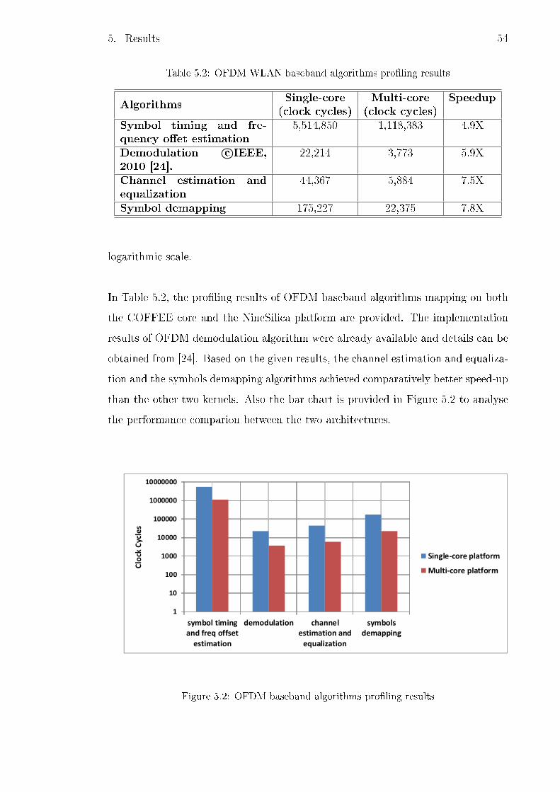
5. Results 54
Table 5.2: OFDM WLAN baseband algorithms pro�ling results
AlgorithmsSingle-core Multi-core Speedup
(clock cycles) (clock cycles)Symbol timing and fre-quency o�et estimation
5,514,850 1,118,383 4.9X
Demodulation c©IEEE,2010 [24].
22,214 3,773 5.9X
Channel estimation andequalization
44,367 5,884 7.5X
Symbol demapping 175,227 22,375 7.8X
logarithmic scale.
In Table 5.2, the pro�ling results of OFDM baseband algorithms mapping on both
the COFFEE core and the NineSilica platform are provided. The implementation
results of OFDM demodulation algorithm were already available and details can be
obtained from [24]. Based on the given results, the channel estimation and equaliza-
tion and the symbols demapping algorithms achieved comparatively better speed-up
than the other two kernels. Also the bar chart is provided in Figure 5.2 to analyse
the performance comparion between the two architectures.
1
10
100
1000
10000
100000
1000000
10000000
symbol timingand freq offset
estimation
demodulation channelestimation and
equalization
symbolsdemapping
Clo
ck C
ycle
s
Single-core platform
Multi-core platform
Figure 5.2: OFDM baseband algorithms pro�ling results

5. Results 55
If we consider the bar charts for both the cases of WCDMA and OFDM baseband
receivers, initial synchronization process seems to be the most time consuming part
like multipath estimation kernel execution of WCDMA receiver and symbol timing
and frequency o�set estimation kernel for the case of OFDM receiver. Taking into
account the real time requirements, each OFDM symbol should be processed in 4µs
while for the case of WCDMA standard, each slot's duration is about 667µs. Con-
sidering the synthesis frequency of 180MHz on an Altera Stratix IV FPGA device,
the WCDMA baseband algorithms of multipath estimation, demodulation, chan-
nel estimation and symbols demapping took execution times of about 34ms, 3.2ms,
0.8ms and 0.35ms respectively. For the case of OFDM WLAN baseband algorithms
like symbol timing and frequency o�set estimation, demodulation, channel estima-
tion and symbols demapping took execution times of 6ms, 21µs, 33µs and 124µs
respectively.
It is quite evident from the obtained execution times that the execution perfor-
mance doesn't meet the real time requirements for both the standards. Considering
the computational requirements of the algorithms, it is not possible for a general
purpose processor to satisfy the strict timing requirements. From the hardware per-
pective, various steps can be taken to improve the performance like by increasing
the number of processing nodes or by increasing the system clock frequency. Also
hardware accelerators can be incorporated in the platform to satisfy the real time
requirements like CGRAs, VLIW or DSP processors.

56
6. CONCLUSION
The performance of digital signal processors (DSPs) and general purpose processors
has improved in the past many years along with reduction in their costs. But still the
operational power is insu�cient to meet the real time requirements of the wireless
standards. Multiprocessor architectures are now becoming an important subject
of the current research and are being considered as one of the prime candidates
for wireless applications requiring computationally intensive tasks. In MPSoC plat-
forms, performance is achieved by distributing or parallelizing the workload among
available computational resources. Practical issues like distributing the algorithms
among the processors besides task management and synchronization issues are of
signi�cant concern. Based on the hardware architecture, the proper allocation of re-
sources is of utmost importance and it depends upon the functional requirements of
the application. For instance, DSPs are good candidates to process high-speed signal
processing algorithms while on the other hand CPUs are good for simple task control
and management. The bottleneck to achieve real-time performance is the commu-
nication overhead between resources like CPUs and DSPs and the response times
of interrupts. Multicasting and broadcasting mitigates the unnecessary communica-
tion overhead when nodes are connected in di�erent communication topologies like
using NoC or other general network communication schemes.
Based on the computational requirements of the most often used modulation schemes
in wireless standards, manufacturers provided di�erent options considering the mar-
ket challenges. Multiprocessor platforms are one of the favorite candidates for this
sort of applications and have proved themselves to be powerful computing engines.
The complexity of wireless terminal implementation increases due to the multi-
standard systems which demands for e�ective design methodologies. Tight time-
to-market constraint can be tackled using programmable components and re-use of

6. Conclusion 57
existing standard software and hardware solutions. Real time requirements can be
met using specialized or dedicated hardware accelerators within a single system-on-
chip (SoC) design but meeting timing constraints using general purpose processors
may require hundreds of processors if operated using lower frequencies. Using higher
frequencies may lead to higher dynamic power consumption which is not very much
recommended for embedded applications. Identifying the software and hardware re-
quirements for multiple wireless standards can help tailor the SDR platform design
and implementation of software components which can be re-used across di�erent
products.
In this thesis work, the baseband algorithms implemented for WCDMA standard
are multipath estimation, demodulation, channel estimation and symbols demap-
ping. For OFDM WLAN standard, the algorithms implemented are symbol timing
and frequency o�set estimation, channel estimation and symbols demapping. If we
compare the performance di�erences between the single core and multi-core archi-
tectures, the WCDMA algorithms of multipath estimation, demodulation, channel
estimation and symbols demapping achieved 8x, 7.7x, 4x and 5.4x speed ups respec-
tively. While OFDM algorithms of symbol timing and frequency o�set estimation,
channel estimation and symbols demapping achieved the speed ups of 4.9x, 7.5x
and 7.8x respectively. Considering the speed ups achieved for mapping individual
baseband algorithms, WCDMA got an overall speed up of 6.3X while OFDM got
an overall speed up of 6.5X. Taking into account the number of processing nodes
of the platform, the overall speed ups achieved are close to theoretical maximum.
The theoretical performance improvement cannot be achieved because of overheads
like interrupts latencies and communication among resources. The scalability of the
homogeneous MPSoC platform brings performance improvement by enabling con-
current execution of identical operations in the processing cores. The pro�ling data
revealed that by using the NineSilica platform, performance improvements can be
obtained by exploiting the platform's inherent parallelism.

58
REFERENCES
[1] Ihmig, M., Herkersdorf, A., "Flexible multi-standard multi-channel system ar-
chitecture for Software De�ned Radio receiver," 9th International Conference
on Intelligent Transport Systems Telecommunications,(ITST), 2009, pp.598-
603, 20-22 Oct. 2009
[2] Jalier, C., Lattard, D., Sassatelli, G., Benoit, P., Torres, L., "Flexible and
distributed real-time control on a 4G telecom MPSoC," Proceedings of 2010
IEEE International Symposium on Circuits and Systems (ISCAS), pp.3961-
3964, May 30 2010-June 2 2010
[3] Garzia, F., Hussain, W., Airoldi, R., Nurmi, J., "A recon�gurable SoC tailored
to Software De�ned Radio applications," NORCHIP, 2009 , pp.1-4, 16-17 Nov.
2009
[4] Wolf, W., Jerraya, A.A., Martin, G., "Multiprocessor System-on-Chip (MP-
SoC) Technology," IEEE Transactions on Computer-Aided Design of Integrated
Circuits and Systems, vol.27, no.10, pp.1701-1713, Oct. 2008
[5] Beigne, E., Clermidy, F., Miermont, S., Vivet, P., "Dynamic Voltage and Fre-
quency Scaling Architecture for Units Integration within a GALS NoC," Second
ACM/IEEE International Symposium on Networks-on-Chip, 2008. NoCS 2008.,
pp.129-138, 7-10 April 2008
[6] Jalier, C., Lattard, D., Jerraya, A.A., Sassatelli, G., Benoit, P., Torres, L.,
"Heterogeneous vs homogeneous MPSoC approaches for a Mobile LTE mo-
dem," Design, Automation & Test in Europe Conference & Exhibition (DATE),
2010, pp.184-189, 8-12 March 2010
[7] Di Stefano, A., Fiscelli, G., Giaconia, C.G., "An FPGA-Based Software De�ned
Radio Platform for the 2.4GHz ISM Band," Research in Microelectronics and
Electronics 2006, Ph. D., pp.73-76.
[8] Holma, H. and Toskala, A. , WCDMA for UMTS: Radio Access for Third
Generation Mobile Communications, Copyright 2000, John Wiley and Sons
Ltd, Ba�ns Lane Chichester, West Sussex, PO19 1UD, England.
[9] Tanner, R. and Woodard, J. , WCDMA:Requirements and Practical Design,
Copyright 2004, John Wiley and Sons Ltd, The Atrium, Southern Gate, Chich-
ester, West Sussex, PO19 8SQ, England.
[10] Richardson, A., WCDMA:Design Handbook, Copyright 2005, Cambridge Uni-
versity Press, The Edinburgh Building, Cambridge CB2 8RU, UK.

REFERENCES 59
[11] Harju, L., Nurmi, J., "Hardware platform for software-de�ned
WCDMA/OFDM baseband receiver implementation," Computers & Dig-
ital Techniques, IET , vol.1, no.5, pp.640-652, Sept. 2007
[12] Harju, L., Nurmi, J., "A baseband receiver architecture for UMTS-WLAN in-
terworking applications", Proceedings. ISCC 2004. Ninth International Sympo-
sium on Computers and Communications, 2004., vol.2, pp. 678- 685, 28 June-1
July 2004
[13] Grayver, E., Frigon, J.-F., Eltawil, A.M., Tarighat, A., Shoarinejad, K., Ab-
basfar, A., Cabric, D., Daneshrad, B., "Design and VLSI implementation for
a WCDMA multipath searcher," IEEE Transactions on Vehicular Technology,
vol.54, no.3, pp. 889- 902, May 2005
[14] Bastug, A., Montalbano, G., Slock, D., "Common and Dedicated Pilot-Based
Channel Estimates Combining and Kalman Filtering for WCDMA Terminals,"
Conference Record of the Thirty-Ninth Asilomar Conference on Signals, Sys-
tems and Computers, 2005., pp.111-115, Oct. 28 2005-Nov. 1 2005
[15] Taewon Hwang, Chenyang Yang, Gang Wu, Shaoqian Li, Li, G.Y., "OFDM
and Its Wireless Applications: A Survey," IEEE Transactions on Vehicular
Technology, vol.58, no.4, pp.1673-1694, May 2009
[16] Heiskala, J. and Terry, J. , OFDM Wireless LANs: A Theoretical and Prac-
tical Guide, Copyright 2002 by Sams Publishing, SAMS, 201 West 103rd St.,
Indianapolis, Indiana, 46290 USA.
[17] Supplement to IEEE Standard for Information Technology - Telecommunica-
tions and Information Exchange Between Systems - Local and Metropolitan
Area Networks - Speci�c Requirements. Part 11: Wireless LAN Medium Access
Control (MAC) and Physical Layer (PHY) Speci�cations: High-Speed Physical
Layer in the 5 GHz Band," IEEE Std 802.11a-1999, 1999.
[18] Garzia, F., Airoldi, R., Ahonen, T., Nurmi, J., Milojevic, D., "Implementation
of the W-CDMA cell search on a MPSOC designed for software de�ned radios,"
IEEE Workshop on Signal Processing Systems, SiPS 2009, pp.030-035, 7-9 Oct.
2009.
[19] Kylliainen, J., Nurmi, J., Kuulusa, M., "COFFEE - a core for free," Proceed-
ings. International Symposium on System-on-Chip, 2003., pp.17-22, 19-21 Nov.
2003
[20] http://co�ee.tut.�/docs/COFFEE_Core_USER_MANUAL.pdf

REFERENCES 60
[21] COFFEE RISC Core, website: http://co�ee.tut.�/docs/COFFEE
_pipeline.pdf
[22] Airoldi, R., Ahonen, T., Garzia, F., Milojevic, D., Nurmi, J., "Implementation
of W-CDMA Cell Search on a Highly Parallel and Scalable MPSoC", Journal
of Signal Processing Systems for Signal, Image and Video Technology, Springer
US, Vol.64, Issue 1, 2011, pp.137-148.
[23] Airoldi, R., Garzia, F., Anjum, O., Nurmi, J., "Homogeneous MPSoC as base-
band signal processing engine for OFDM systems," International Symposium
on System on Chip (SoC), 2010, pp.26-30, 29-30 Sept. 2010
[24] Airoldi, R., Garzia, F., Nurmi, J., "FFT Algorithms Evaluation on a Homoge-
neous Multi-processor System-on-Chip," in Proc. International Symposium on
Multicore Systems-on-Chip (MCSoC 2010), San Diego, CA, USA, September
13-16, 2010.
[25] Fazal, Rizwan., Hussain, Waqar., Ahonen, Tapani., Nurmi, Jari., "Evaluation of
WCDMA receiver baseband processing on a Multi-Processor System-On-Chip,"
18th International Conference on Digital Signal Processing (DSP), 2013, pp.1-7,
1-3 July 2013
Related Documents