Rev. 1.00 1 October 16, 2014 HT82V73A 1500mW Audio Power Amp with Shutdown Features • Operating voltage: 2.2V to 5.5V • High signal-to-noise ratio • Low distortion • Large output voltage swing • Low power consumption • Output power 1500mW at 10% THD+N into 8Ω (VDD=5V) • Wide temperature operating range • Low power-on and chip enable or disable POP noise • Low standby current • Power off control • Can directly drive speakers • 8-pin SOP package Applications • Wide range of audio applications General Description The HT82V73A is an integrated class AB mono speaker driver contained in an SOP 8-pin package. The device is capable of delivering 1500mW of output power into an 8Ω load with less than 10% (THD+N) distortion from a 5V power supply. When in the shutdown mode the very low standby current is an important feature for a wide range of battery powered audio applications. Block Diagram O U T N V S S O U T P C E A M P 1 B I A S R A M P 2 R 1 0 R A u d I n V R E F V D D R Pin Assignment 1 2 3 4 8 7 6 5 O U T N A u d I n V R E F V S S H T 8 2 V 7 3 A 8 S O P - A ( E P A D ) V D D O U T P N C C E G N D P A D

Welcome message from author
This document is posted to help you gain knowledge. Please leave a comment to let me know what you think about it! Share it to your friends and learn new things together.
Transcript

Rev. 1.00 1 October 16, 2014 Rev. 1.00 PB October 16, 2014
HT82V73A1500mW Audio Power Amp with Shutdown
Features• Operatingvoltage:2.2Vto5.5V• Highsignal-to-noiseratio• Lowdistortion• Largeoutputvoltageswing• Lowpowerconsumption• Outputpower1500mWat10%THD+Ninto8Ω(VDD=5V)
• Widetemperatureoperatingrange• Lowpower-onandchipenableordisablePOPnoise• Lowstandbycurrent• Poweroffcontrol• Candirectlydrivespeakers• 8-pinSOPpackage
Applications• Widerangeofaudioapplications
General DescriptionTheHT82V73A is an integrated classABmonospeakerdrivercontained inanSOP8-pinpackage.The device is capable of delivering 1500mWofoutputpower intoan8Ω loadwith less than10%(THD+N)distortionfroma5Vpowersupply.Whenin theshutdownmodetheverylowstandbycurrentisan important feature forawide rangeofbatterypoweredaudioapplications.
Block Diagram
Pin Assignment
Rev. 1.00 2 October 16, 2014 Rev. 1.00 3 October 16, 2014
HT82V73A1500mW Audio Power Amp with Shutdown
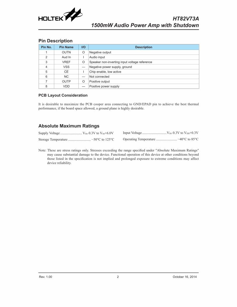
Pin DescriptionPin No. Pin Name I/O Description
1 OUTN O Negative output2 Aud In I Audio input3 VREF O Speaker non-inverting input voltage reference4 VSS — Negative power supply, ground5 CE I Chip enable, low active6 NC — Not connected7 OUTP O Positive output8 VDD — Positive power supply
PCB Layout Consideration
It isdesirable tomaximize thePCBcooperareaconnecting toGND/EPADpin toachieve thebest thermalperformance,iftheboardspaceallowed,agroundplaneishighlydesirable.
Absolute Maximum RatingsSupplyVoltage......................... VSS−0.3VtoVSS+6.0V
StorageTemperature.......................... −50°Cto125°C
InputVoltage............................VSS−0.3VtoVDD+0.3V
OperatingTemperature........................ −40°Cto85°C
Note:Thesearestressratingsonly.Stressesexceedingtherangespecifiedunder″AbsoluteMaximumRatings″maycausesubstantialdamagetothedevice.Functionaloperationofthisdeviceatotherconditionsbeyondthoselistedin thespecificationisnot impliedandprolongedexposuretoextremeconditionsmayaffectdevicereliability.
Rev. 1.00 3 October 16, 2014
HT82V73A
Rev. 1.00 2 October 16, 2014 Rev. 1.00 3 October 16, 2014
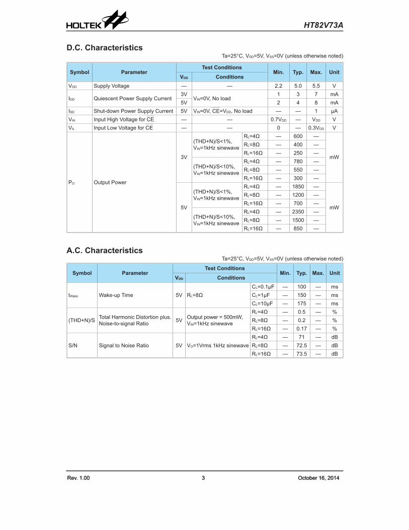
D.C. CharacteristicsTa=25°C, VDD=5V, VSS=0V (unless otherwise noted)
Symbol ParameterTest Conditions
Min. Typ. Max. UnitVDD Conditions
VDD Supply Voltage — — 2.2 5.0 5.5 V
IDD Quiescent Power Supply Current3V
VIN=0V, No load1 3 7 mA
5V 2 4 8 mAISD Shut-down Power Supply Current 5V VIN=0V, CE=VDD, No load — — 1 µAVIH Input High Voltage for CE — — 0.7VDD — VDD VVIL Input Low Voltage for CE — — 0 — 0.3VDD V
PO Output Power
3V
(THD+N)/S<1%, VIN=1kHz sinewave
RL=4Ω — 600 —
mW
RL=8Ω — 400 —RL=16Ω — 250 —
(THD+N)/S<10%, VIN=1kHz sinewave
RL=4Ω — 780 —RL=8Ω — 550 —RL=16Ω — 300 —
5V
(THD+N)/S<1%, VIN=1kHz sinewave
RL=4Ω — 1850 —
mW
RL=8Ω — 1200 —RL=16Ω — 700 —
(THD+N)/S<10%, VIN=1kHz sinewave
RL=4Ω — 2350 —RL=8Ω — 1500 —RL=16Ω — 850 —
A.C. CharacteristicsTa=25°C, VDD=5V, VSS=0V (unless otherwise noted)
Symbol ParameterTest Conditions
Min. Typ. Max. UnitVDD Conditions
tWake Wake-up Time 5V RL=8ΩCL=0.1µF — 100 — msCL=1µF — 150 — msCL=10µF — 175 — ms
(THD+N)/S Total Harmonic Distortion plus. Noise-to-signal Ratio 5V Output power = 500mW,
VIN=1kHz sinewave
RL=4Ω — 0.5 — %RL=8Ω — 0.2 — %RL=16Ω — 0.17 — %
S/N Signal to Noise Ratio 5V VO=1Vrms 1kHz sinewaveRL=4Ω — 71 — dBRL=8Ω — 72.5 — dBRL=16Ω — 73.5 — dB
Rev. 1.00 4 October 16, 2014
HT82V73A
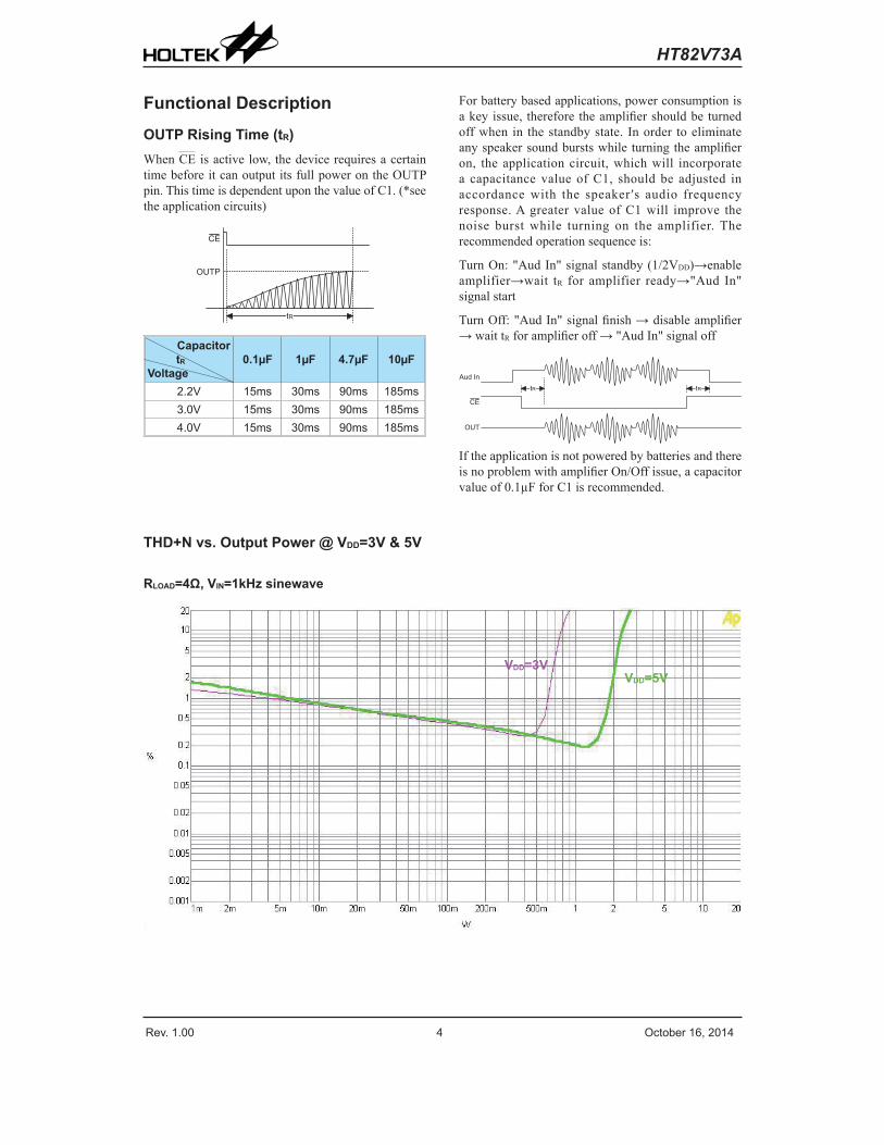
THD+N vs. Output Power @ VDD=3V & 5V
RLOAD=4Ω, VIN=1kHz sinewave
Functional Description
OUTP Rising Time (tR)WhenCEisactivelow,thedevicerequiresacertaintimebeforeitcanoutputitsfullpowerontheOUTPpin.ThistimeisdependentuponthevalueofC1.(*seetheapplicationcircuits)
CapacitortR
Voltage0.1µF 1µF 4.7µF 10µF
2.2V 15ms 30ms 90ms 185ms3.0V 15ms 30ms 90ms 185ms4.0V 15ms 30ms 90ms 185ms
Forbatterybasedapplications,powerconsumptionisakeyissue, thereforetheamplifiershouldbeturnedoffwhen in thestandbystate. Inorder toeliminateanyspeakersoundburstswhileturningtheamplifieron, theapplicationcircuit,whichwill incorporatea capacitancevalueofC1, shouldbe adjusted inaccordancewith the speaker′s audio frequencyresponse.AgreatervalueofC1will improve thenoise burstwhile turning on the amplifier.Therecommendedoperationsequenceis:
TurnOn:"AudIn"signalstandby(1/2VDD)→enableamplifier→wait tR for amplifier ready→"Aud In"signalstart
TurnOff:"AudIn"signalfinish→disableamplifier→waittRforamplifieroff→"AudIn"signaloff
IftheapplicationisnotpoweredbybatteriesandthereisnoproblemwithamplifierOn/Offissue,acapacitorvalueof0.1µFforC1isrecommended.
VDD=3VVDD=5V

Rev. 1.00 5 October 16, 2014
HT82V73A
RLOAD=8Ω, VIN=1kHz sinewave
RLOAD=16Ω, VIN=1kHz sinewave
VDD=3V
VDD=3V
VDD=5V
VDD=5V
Rev. 1.00 6 October 16, 2014
HT82V73A
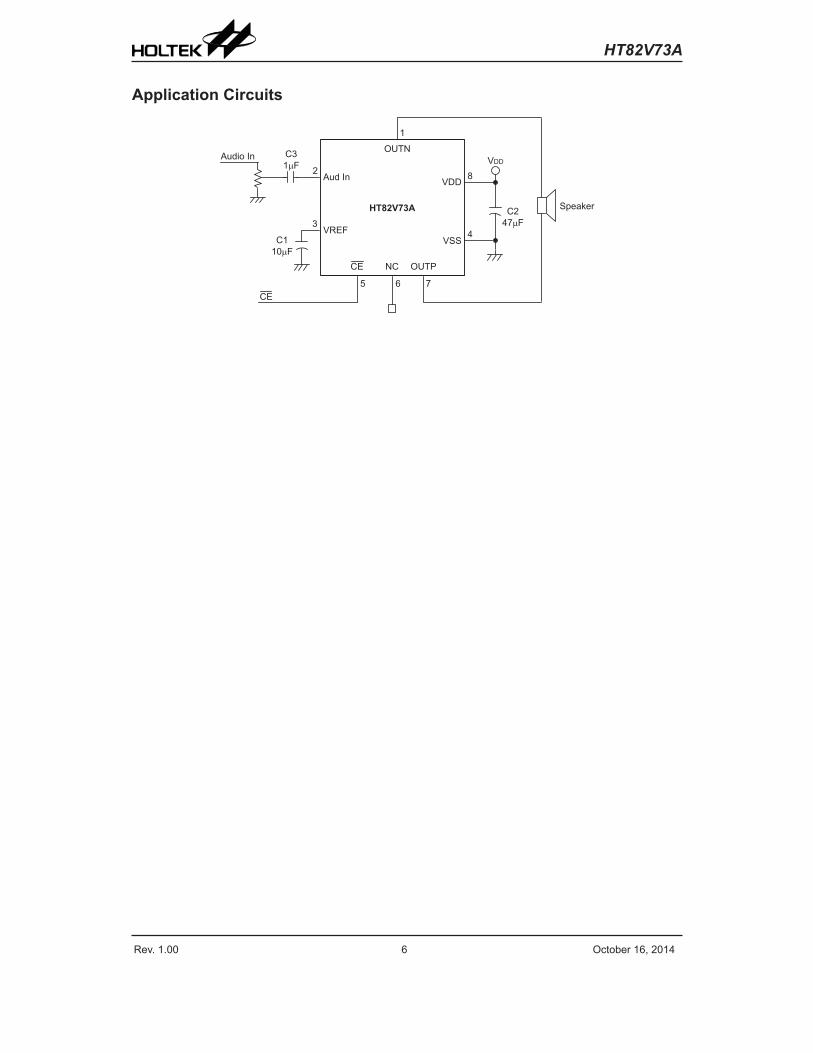
Application Circuits

Rev. 1.00 7 October 16, 2014
HT82V73A
Package InformationNotethat thepackageinformationprovidedhereisforconsultationpurposesonly.Asthis informationmaybeupdatedatregularintervalsusersareremindedtoconsulttheHoltekwebsiteforthelatestversionofthepackageinformation.
Additionalsupplementaryinformationwithregardtopackagingislistedbelow.Clickontherelevantsectiontobetransferredtotherelevantwebsitepage.
• FurtherPackageInformation(includeOutlineDimensions,ProductTapeandReelSpecifications)
• PackingMeterialsInformation
• Cartoninformation
Rev. 1.00 8 October 16, 2014
HT82V73A
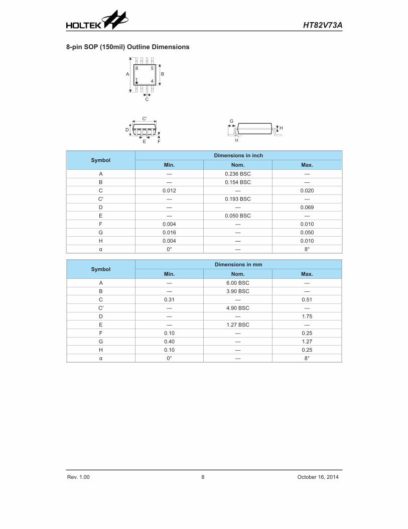
8-pin SOP (150mil) Outline Dimensions
SymbolDimensions in inch
Min. Nom. Max.A — 0.236 BSC —B — 0.154 BSC —C 0.012 — 0.020C′ — 0.193 BSC —D — — 0.069E — 0.050 BSC —F 0.004 — 0.010G 0.016 — 0.050H 0.004 — 0.010α 0° — 8°
SymbolDimensions in mm
Min. Nom. Max.A — 6.00 BSC —B — 3.90 BSC —C 0.31 — 0.51C′ — 4.90 BSC —D — — 1.75E — 1.27 BSC —F 0.10 — 0.25G 0.40 — 1.27H 0.10 — 0.25α 0° — 8°
Rev. 1.00 9 October 16, 2014
HT82V73A
Copyright© 2014 by HOLTEK SEMICONDUCTOR INC.
The information appearing in this Data Sheet is believed to be accurate at the time of publication. However, Holtek assumes no responsibility arising from the use of the specifications described. The applications mentioned herein are used solely for the purpose of illustration and Holtek makes no warranty or representation that such applications will be suitable without further modification, nor recommends the use of its products for application that may present a risk to human life due to malfunction or otherwise. Holtek's products are not authorized for use as critical components in life support devices or systems. Holtek reserves the right to alter its products without prior notification. For the most up-to-date information, please visit our web site at http://www.holtek.com.tw.
Related Documents