Application Note R01AN3516EJ0100 Rev.1.00 Page 1 of 43 Mar.10.20 RX Family Flash ROM Correction Summary With large-capacity flash memory or when performing low-speed serial programming on a user system, it can take considerable time to rewrite all of the flash memory. This application note describes a method of flash ROM correction in which patches are applied to the user program in a manner that rewrites the smallest area possible. Unless otherwise specified, the descriptions in this application note apply to the RX113. Target Device RX113 Group When using this application note with other Renesas MCUs, careful evaluation is recommended after making modifications to match the specifications of the alternative MCU. Contents 1. Specifications ............................................................................................................................ 3 2. Operation Confirmation Conditions ........................................................................................... 5 3. Related Application Notes ......................................................................................................... 6 4. Software .................................................................................................................................... 7 4.1 Operation Overview................................................................................................................................. 7 4.1.1 Table Data Area and Patch Area Checking .......................................................................................... 8 4.1.2 ROM Correction Flowchart .................................................................................................................... 9 4.1.3 Rewrite with BRK Instruction Flowchart .............................................................................................. 10 4.1.4 Copy Area Rewrite Procedure............................................................................................................. 11 4.1.5 Rewrite with BRK Instruction Procedure ............................................................................................. 12 4.1.6 Write Procedure for Flags with Allocated Reserved Areas ................................................................. 13 4.1.7 Identifying BRK Exception (Unconditional Trap) Occurrence Address ............................................... 14 4.1.8 Determination of Patch Processing to Be Run from Address where BRK Exception Occurred ......... 15 4.1.9 Return Setting from BRK Exception Handler ...................................................................................... 16 4.1.10 Patch Program Execution and Return to User Program ..................................................................... 17 4.2 Required Memory Sizes ........................................................................................................................ 18 4.3 File and Folder Structure ....................................................................................................................... 18 4.3.1 src Folder............................................................................................................................................. 19 4.3.2 src\r_bsp Folder .................................................................................................................................. 19 4.3.3 src\r_config Folder............................................................................................................................... 19 4.3.4 src\r_flash_rx Folder............................................................................................................................ 19 4.3.5 src\r_rom_correct Folder ..................................................................................................................... 19

Welcome message from author
This document is posted to help you gain knowledge. Please leave a comment to let me know what you think about it! Share it to your friends and learn new things together.
Transcript
Application Note
R01AN3516EJ0100 Rev.1.00 Page 1 of 43 Mar.10.20
RX Family Flash ROM Correction Summary With large-capacity flash memory or when performing low-speed serial programming on a user system, it can take considerable time to rewrite all of the flash memory. This application note describes a method of flash ROM correction in which patches are applied to the user program in a manner that rewrites the smallest area possible.
Unless otherwise specified, the descriptions in this application note apply to the RX113.
Target Device RX113 Group
When using this application note with other Renesas MCUs, careful evaluation is recommended after making modifications to match the specifications of the alternative MCU.
Contents
1. Specifications ............................................................................................................................ 3
2. Operation Confirmation Conditions ........................................................................................... 5
3. Related Application Notes ......................................................................................................... 6
4. Software .................................................................................................................................... 7 4.1 Operation Overview ................................................................................................................................. 7 4.1.1 Table Data Area and Patch Area Checking .......................................................................................... 8 4.1.2 ROM Correction Flowchart .................................................................................................................... 9 4.1.3 Rewrite with BRK Instruction Flowchart .............................................................................................. 10 4.1.4 Copy Area Rewrite Procedure............................................................................................................. 11 4.1.5 Rewrite with BRK Instruction Procedure ............................................................................................. 12 4.1.6 Write Procedure for Flags with Allocated Reserved Areas ................................................................. 13 4.1.7 Identifying BRK Exception (Unconditional Trap) Occurrence Address ............................................... 14 4.1.8 Determination of Patch Processing to Be Run from Address where BRK Exception Occurred ......... 15 4.1.9 Return Setting from BRK Exception Handler ...................................................................................... 16 4.1.10 Patch Program Execution and Return to User Program ..................................................................... 17 4.2 Required Memory Sizes ........................................................................................................................ 18 4.3 File and Folder Structure ....................................................................................................................... 18 4.3.1 src Folder ............................................................................................................................................. 19 4.3.2 src\r_bsp Folder .................................................................................................................................. 19 4.3.3 src\r_config Folder ............................................................................................................................... 19 4.3.4 src\r_flash_rx Folder ............................................................................................................................ 19 4.3.5 src\r_rom_correct Folder ..................................................................................................................... 19
RX Family Flash ROM Correction
R01AN3516EJ0100 Rev.1.00 Page 2 of 43 Mar.10.20
4.4 Option-Setting Memory ......................................................................................................................... 20 4.5 Constants .............................................................................................................................................. 21 4.6 Structure Listing..................................................................................................................................... 22 4.7 Enumeration Listing ............................................................................................................................... 22 4.8 Variables ................................................................................................................................................ 23 4.9 Functions ............................................................................................................................................... 23 4.10 Function Specifications ......................................................................................................................... 24
5. Precautions .............................................................................................................................. 31 5.1 Precautions When Using This Application Note .................................................................................... 31 5.2 Table Data Area and Patch Area Write Procedure Examples .............................................................. 31 5.3 Adapting Specifications to Other Products ............................................................................................ 34
6. Creating Data for Table Data Area and Patch Area ................................................................ 36 6.1 Patch Area Data Creation Example ...................................................................................................... 36 6.2 Example of Procedure for Exporting Data from Patch Area ................................................................. 39
7. Sample Code ........................................................................................................................... 42
8. Reference Documents ............................................................................................................. 42
Revision History .............................................................................................................................. 43
RX Family Flash ROM Correction
R01AN3516EJ0100 Rev.1.00 Page 3 of 43 Mar.10.20
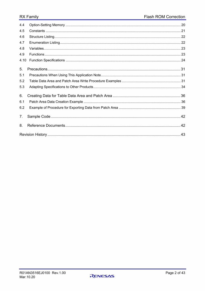
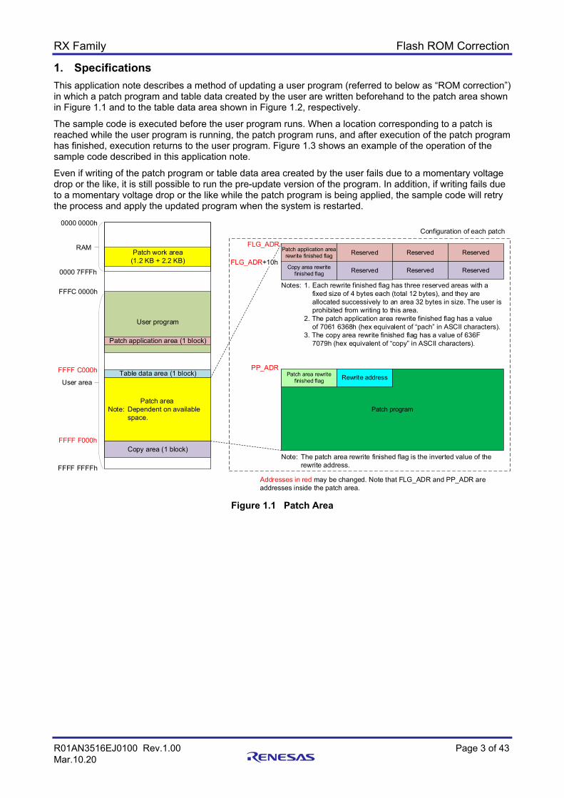
1. Specifications This application note describes a method of updating a user program (referred to below as “ROM correction”) in which a patch program and table data created by the user are written beforehand to the patch area shown in Figure 1.1 and to the table data area shown in Figure 1.2, respectively.
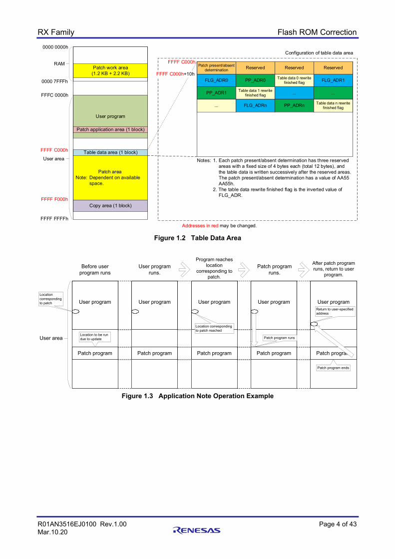
The sample code is executed before the user program runs. When a location corresponding to a patch is reached while the user program is running, the patch program runs, and after execution of the patch program has finished, execution returns to the user program. Figure 1.3 shows an example of the operation of the sample code described in this application note.
Even if writing of the patch program or table data area created by the user fails due to a momentary voltage drop or the like, it is still possible to run the pre-update version of the program. In addition, if writing fails due to a momentary voltage drop or the like while the patch program is being applied, the sample code will retry the process and apply the updated program when the system is restarted.
Figure 1.1 Patch Area
Patch work area (1.2 KB + 2.2 KB)
User program
Patch application area (1 block)
Table data area (1 block)
Patch area Note: Dependent on available
space.
RAM
User area
0000 0000h
0000 7FFFh
FFFC 0000h
FFFF FFFFh
Patch application area rewrite finished flag
Patch program
FLG_ADR
FLG_ADR+10h
PP_ADR
Copy area (1 block)
Reserved Reserved Reserved
FFFF F000h
Patch area rewrite finished flag Rewrite address
Copy area rewrite finished flag Reserved Reserved Reserved
Notes: 1. Each rewrite finished flag has three reserved areas with a fixed size of 4 bytes each (total 12 bytes), and they are allocated successively to an area 32 bytes in size. The user is prohibited from writing to this area.
2. The patch application area rewrite finished flag has a value of 7061 6368h (hex equivalent of “pach” in ASCII characters).
3. The copy area rewrite finished flag has a value of 636F 7079h (hex equivalent of “copy” in ASCII characters).
Configuration of each patch
Note: The patch area rewrite finished flag is the inverted value of the rewrite address.
Addresses in red may be changed. Note that FLG_ADR and PP_ADR are addresses inside the patch area.
FFFF C000h
RX Family Flash ROM Correction
R01AN3516EJ0100 Rev.1.00 Page 4 of 43 Mar.10.20
Figure 1.2 Table Data Area
User program
Patch program
User area
User program
Patch program
Location corresponding to patch
Location to be run due to update
User program
Patch program
User program
Patch program
Before user program runs
User program
Patch program
User program runs.
Program reaches location
corresponding to patch.
Patch program runs.
After patch program runs, return to user
program.
Location corresponding to patch reached
Patch program runs
Return to user-specified address
Patch program ends
Figure 1.3 Application Note Operation Example
Patch present/absent determination
FLG_ADR0 PP_ADR0 Table data 0 rewrite finished flag FLG_ADR1
Patch work area (1.2 KB + 2.2 KB)
User program
Patch application area (1 block)
Table data area (1 block)
Patch area Note: Dependent on available
space.
RAM
User area
0000 0000h
0000 7FFFh
FFFC 0000h
FFFF FFFFh
Copy area (1 block)FFFF F000h
FFFF C000h
Configuration of table data area
FFFF C000h
FFFF C000h+10hReserved Reserved Reserved
PP_ADR1 Table data 1 rewrite finished flag ... ...
... FLG_ADRn PP_ADRn Table data n rewrite finished flag
Notes: 1. Each patch present/absent determination has three reserved areas with a fixed size of 4 bytes each (total 12 bytes), and the table data is written successively after the reserved areas. The patch present/absent determination has a value of AA55 AA55h.
2. The table data rewrite finished flag is the inverted value of FLG_ADR.
Addresses in red may be changed.
RX Family Flash ROM Correction
R01AN3516EJ0100 Rev.1.00 Page 5 of 43 Mar.10.20
2. Operation Confirmation Conditions Table 2.1 lists the conditions under which the operation of the sample code referenced in this application note has been confirmed.
Table 2.1 Operation Confirmation Conditions
Item Description MCU used R5F51138AFP (RX113 Group) Operating frequencies Main clock: 16 MHz
Subclock stopped PLL: 32 MHz (main clock: × 1/4 × 8) HOCO stopped System clock (ICLK): 32 MHz (PLL × 1/1) FlashIF clock (FCLK): 32 MHz (PLL × 1/1)
Operating voltage 3.3 V Integrated development environment
Renesas Electronics e2 studio Version 7.7.0
C compiler Renesas Electronics C/C++ Compiler Package for RX Family V3.02.00
Compiler option Default settings of integrated development environment
iodefine.h version Ver. 1.1 Endian order Little endian or big endian Operating mode Single-chip mode Processor mode Supervisor mode Sample code version Version 1.00 Board used Renesas Starter Kit for RX113 (product number: R0K505113C010BR)
RX Family Flash ROM Correction
R01AN3516EJ0100 Rev.1.00 Page 6 of 43 Mar.10.20
3. Related Application Notes Application notes related to this application note are listed below. Refer to them in conjunction with this application note.
• RX Family Board Support Package Module Using Firmware Integration Technology (R01AN1685) • RX Family Flash Module Using Firmware Integration Technology (R01AN2184) Sample code from the above application notes is incorporated into the sample code accompanying this application note. If a newer version is available, use it instead. Visit the Renesas Electronics Corporation website to check for and download the latest version.
RX Family Flash ROM Correction
R01AN3516EJ0100 Rev.1.00 Page 7 of 43 Mar.10.20
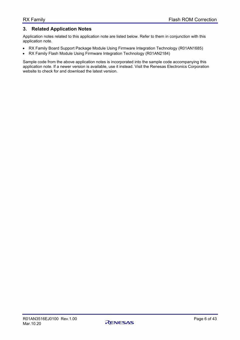
4. Software 4.1 Operation Overview To use ROM correction, create a table data area and patch area to match your specifications. Note that the sample code imposes an upper limit of four on the number of times the patch present/absent determination, patch application area rewrite finished flag, and copy area rewrite finished flag may be written.
Figure 4.1 Table Data Area for ROM Correction
Execute the sample code before running the user program. After the processing corresponding to the patch area and table data area created by the user completes, the user program is run. Figure 4.2 is a flowchart of operation when the sample code is used.
Figure 4.2 Flowchart of Operation Using Sample Code
AA55 AA55h
FLG_ADR0 PP_ADR0 Table data 0 rewrite finished flag FLG_ADR1
Patch work area (1.2 KB + 2.2 KB)
User program
Patch application area (1 block)
Table data area (1 block)
Patch area Note: Dependent on available
space.
RAM
User area
0000 0000h
0000 7FFFh
FFFC 0000h
FFFF FFFFh
Copy area (1 block)FFFF F000h
FFFF C000h
FFFF C000h
FFFF C000h+10hReserved Reserved Reserved
PP_ADR1 Table data 1 rewrite finished flag ... ...
... FLG_ADRn PP_ADRn Table data n rewrite finished flag
Blank Blank Blank
Patch application area rewrite finished flag
FLG_ADR0
FLG_ADR0+10hReserved Reserved Reserved
Copy area rewrite finished flag Reserved Reserved Reserved
Patch program 0
PP_ADR0Patch area rewrite
finished flag Rewrite address
Patch application area rewrite finished flag
FLG_ADRn
FLG_ADRn+10hReserved Reserved Reserved
Copy area rewrite finished flag Reserved Reserved Reserved
Patch program n
PP_ADRnPatch area rewrite
finished flag Rewrite address
The table data is judged to be finished if the locations corresponding to FLG_ADRx, PP_ADRx, and the table data x rewrite finished flag are all blank.
Addresses in red may be changed.
Start
ROM correction
User program
RX Family Flash ROM Correction
R01AN3516EJ0100 Rev.1.00 Page 8 of 43 Mar.10.20
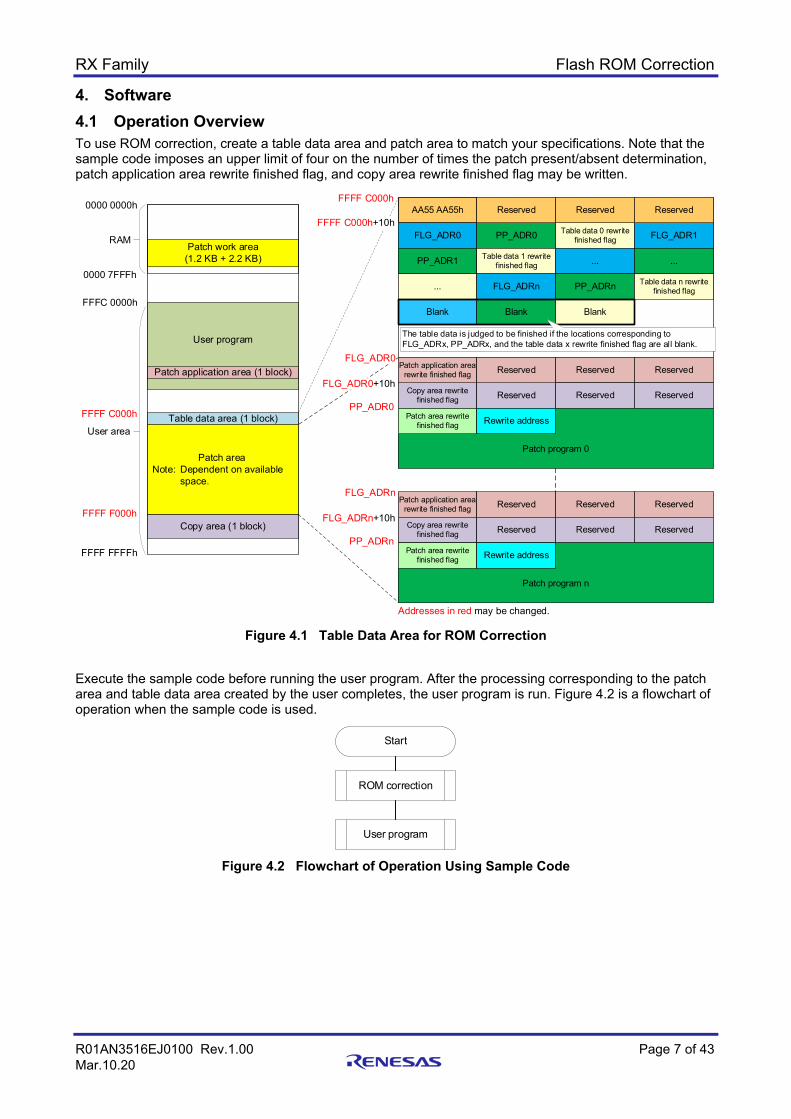
4.1.1 Table Data Area and Patch Area Checking When performing ROM correction, the sample code performs the steps shown in Figure 4.3 to check the table data area and patch area.
Figure 4.3 Table Data Area and Patch Area Checking
Patch present/absent determination
FLG_ADR0 PP_ADR0 Table data 0 rewrite finished flag FLG_ADR1
Patch work area (1.2 KB + 2.2 KB)
User program
Patch application area (1 block)
Table data area (1 block)
Patch area Note: Dependent on available
space.
RAM
User area
0000 0000h
0000 7FFFh
FFFC 0000h
FFFF FFFFh
Copy area (1 block)FFFF F000h
FFFF C000h
FFFF C000h
FFFF C000h+10h Reserved Reserved Reserved
PP_ADR1 Table data 1 rewrite finished flag ... ...
... FLG_ADRn PP_ADRn Table data n rewrite finished flag
Patch program 0
FLG_ADR0
PP_ADR0
Reserved Reserved Reserved
Patch area 0 rewrite finished flag Rewrite address 0
Copy area 0 rewrite finished flag Reserved Reserved Reserved
[5] Check target patch application area.
[1] Check if patch is present/absent.
[4] Check if rewrite of patch area has finished.• If rewrite is finished: inverted value of rewrite
address 0• If rewrite is not finished: blank• If other than above: write failed due to
momentary voltage drop, etc.
[3] Check target patch area.
[2] Check if table data write has finished.
[6] Check if rewrite of patch application area 0 has finished.• If rewrite is finished: 7061 6368h• If rewrite is not finished: blank• If other than above: write failed due to momentary voltage
drop, etc.
Addresses in red may be changed.
Patch application area rewrite finished flag
FLG_ADR0+10h
RX Family Flash ROM Correction
R01AN3516EJ0100 Rev.1.00 Page 9 of 43 Mar.10.20
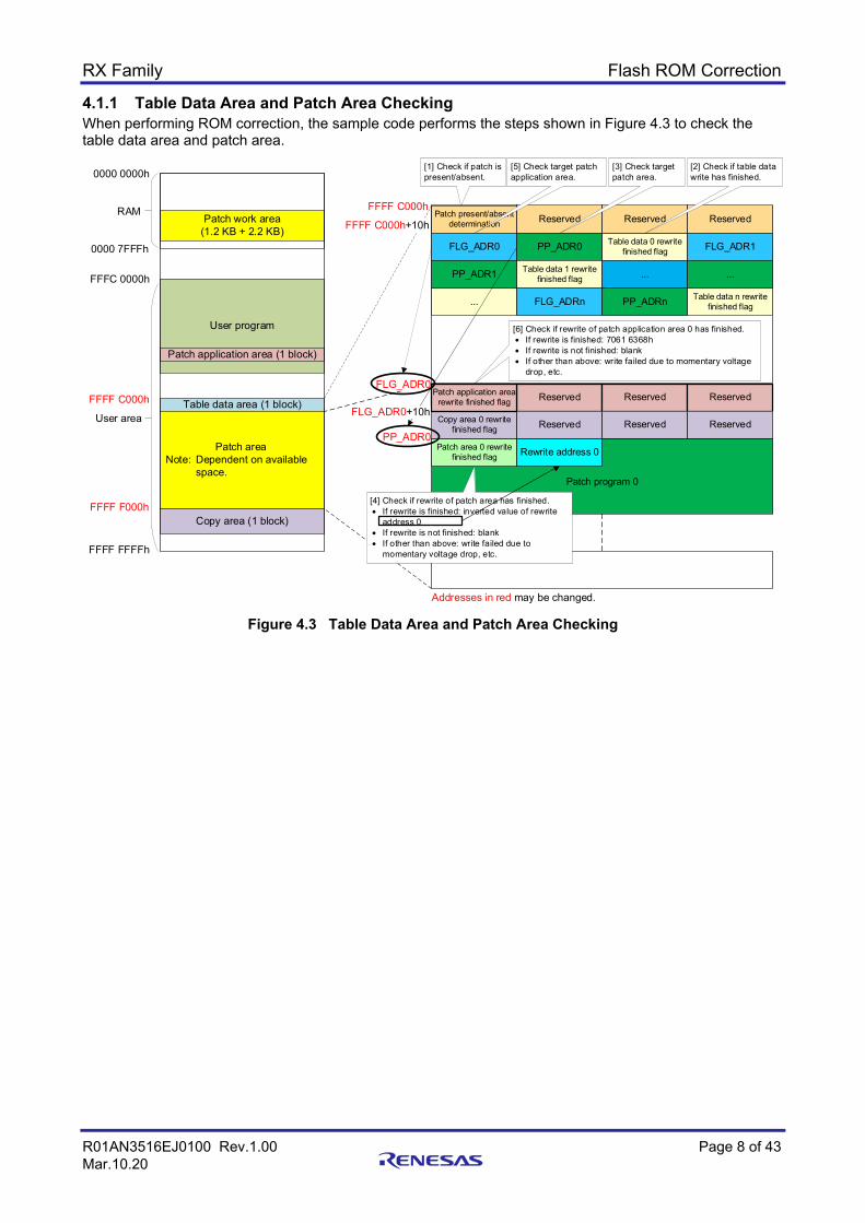
4.1.2 ROM Correction Flowchart Figure 4.4 is a flowchart of ROM correction.
Figure 4.4 ROM Correction Flowchart
ROM correction
AA55AA55h?
Read patch present/absent determination
Rewrite with BRK instruction
No
Yes
tbl_adr = 0, (Write upper limit count − 1)*4, 4
Write upper limit count (= 4)
tbl_adr
y = 0, n, 1
Rewrite finished?
No
Yes
Read table data y rewrite finished flag
y
Read PP_ADRy
Store table data registration count
Read patch area y rewrite finished flag
Rewrite finished?
No
Yes
Read patch application area y rewrite finished flag
Rewrite finished?
No
Yes
z = 0,Write upper limit count − 1,
1
Write upper limit count (= 4)
z
return
Read FLG_ADRy
Blank?
No
Yes (table data finished)
Checks table data.
Checks patch area.
Blank?
No
Yes
Checks if FLG_ADRy, PP_ADRy, and table data y rewrite finished flag areas are all blank.
RX Family Flash ROM Correction
R01AN3516EJ0100 Rev.1.00 Page 10 of 43 Mar.10.20
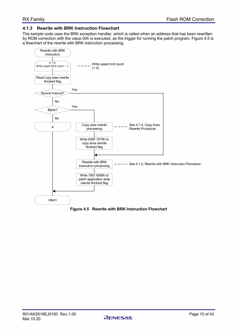
4.1.3 Rewrite with BRK Instruction Flowchart The sample code uses the BRK exception handler, which is called when an address that has been rewritten by ROM correction with the value 00h is executed, as the trigger for running the patch program. Figure 4.5 is a flowchart of the rewrite with BRK instruction processing.
Figure 4.5 Rewrite with BRK Instruction Flowchart
Rewrite with BRK instruction
Rewrite with BRK instruction processing
return
See 4.1.5, Rewrite with BRK Instruction Procedure.
Write 7061 6368h to patch application area
rewrite finished flag
Rewrite finished?Yes
No
Read copy area rewrite finished flag
Copy area rewrite processing
See 4.1.4, Copy Area Rewrite Procedure.
Write 636F 7079h to copy area rewrite
finished flag
Blank?Yes
No
a = 0,Write upper limit count − 1,
1
Write upper limit count (= 4)
a
RX Family Flash ROM Correction
R01AN3516EJ0100 Rev.1.00 Page 11 of 43 Mar.10.20
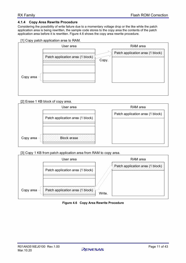
4.1.4 Copy Area Rewrite Procedure Considering the possibility of write failure due to a momentary voltage drop or the like while the patch application area is being rewritten, the sample code stores to the copy area the contents of the patch application area before it is rewritten. Figure 4.6 shows the copy area rewrite procedure.
Figure 4.6 Copy Area Rewrite Procedure
Patch application area (1 block)
User area RAM area
Patch application area (1 block)
User area RAM area
Block erase
Copy.
Patch application area (1 block)
User area RAM area
Patch application area (1 block)
Patch application area (1 block)
Patch application area (1 block)
Patch application area (1 block)
[1] Copy patch application area to RAM.
[2] Erase 1 KB block of copy area.
[3] Copy 1 KB from patch application area from RAM to copy area.
Copy area
Copy area
Copy area Write.
RX Family Flash ROM Correction
R01AN3516EJ0100 Rev.1.00 Page 12 of 43 Mar.10.20
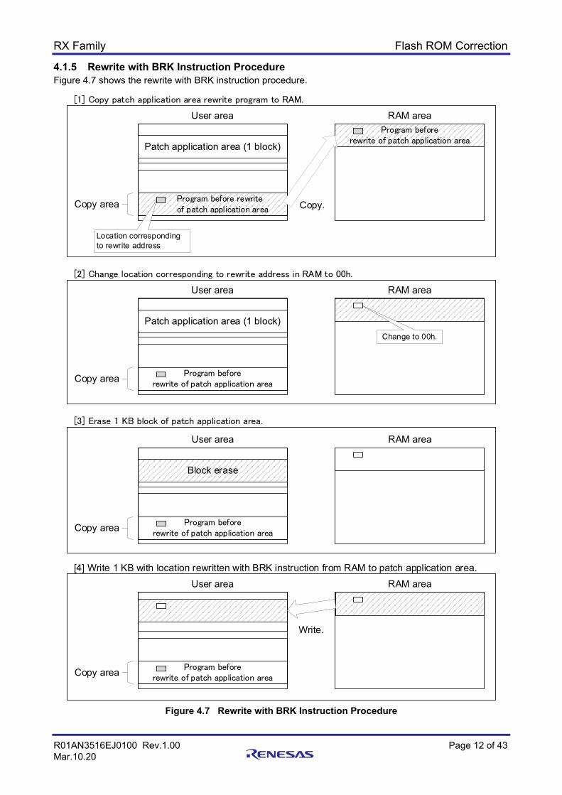
4.1.5 Rewrite with BRK Instruction Procedure Figure 4.7 shows the rewrite with BRK instruction procedure.
Figure 4.7 Rewrite with BRK Instruction Procedure
Patch application area (1 block)
User area RAM area
Program before rewrite of patch application area
Copy area
Patch application area (1 block)
User area RAM area
Program before rewrite of patch application area
Copy.
Block erase
User area RAM area
Program before rewrite of patch application area
Location corresponding to rewrite address
Program before rewrite of patch application area
Change to 00h.
User area RAM area
Program before rewrite of patch application area
Write.
[1] Copy patch application area rewrite program to RAM.
[2] Change location corresponding to rewrite address in RAM to 00h.
[3] Erase 1 KB block of patch application area.
[4] Write 1 KB with location rewritten with BRK instruction from RAM to patch application area.
Copy area
Copy area
Copy area
RX Family Flash ROM Correction
R01AN3516EJ0100 Rev.1.00 Page 13 of 43 Mar.10.20
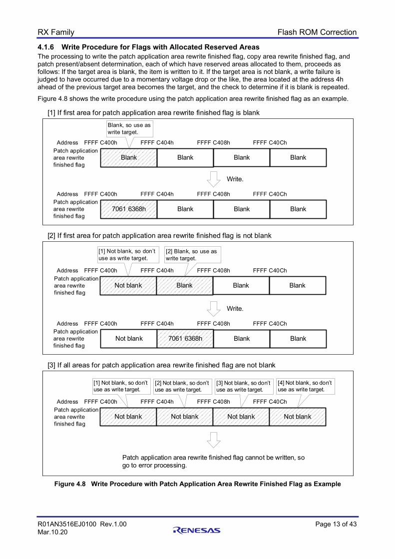
4.1.6 Write Procedure for Flags with Allocated Reserved Areas The processing to write the patch application area rewrite finished flag, copy area rewrite finished flag, and patch present/absent determination, each of which have reserved areas allocated to them, proceeds as follows: If the target area is blank, the item is written to it. If the target area is not blank, a write failure is judged to have occurred due to a momentary voltage drop or the like, the area located at the address 4h ahead of the previous target area becomes the target, and the check to determine if it is blank is repeated.
Figure 4.8 shows the write procedure using the patch application area rewrite finished flag as an example.
Figure 4.8 Write Procedure with Patch Application Area Rewrite Finished Flag as Example
Blank Blank Blank BlankPatch application area rewrite finished flag
Blank, so use as write target.
[1] If first area for patch application area rewrite finished flag is blank
Not blank Blank Blank BlankPatch application area rewrite finished flag
[1] Not blank, so don’t use as write target.
[2] If first area for patch application area rewrite finished flag is not blank
[2] Blank, so use as write target.
Not blank Not blank Not blank Not blankPatch application area rewrite finished flag
[1] Not blank, so don’t use as write target.
[3] If all areas for patch application area rewrite finished flag are not blank
[2] Not blank, so don’t use as write target.
[3] Not blank, so don’t use as write target.
[4] Not blank, so don’t use as write target.
7061 6368h Blank Blank BlankPatch application area rewrite finished flag
Not blank 7061 6368h Blank BlankPatch application area rewrite finished flag
Write.
Write.
Patch application area rewrite finished flag cannot be written, so go to error processing.
FFFF C400h FFFF C404h FFFF C408h FFFF C40ChAddress
FFFF C400h FFFF C404h FFFF C408h FFFF C40ChAddress
FFFF C400h FFFF C404h FFFF C408h FFFF C40ChAddress
FFFF C400h FFFF C404h FFFF C408h FFFF C40ChAddress
FFFF C400h FFFF C404h FFFF C408h FFFF C40ChAddress
RX Family Flash ROM Correction
R01AN3516EJ0100 Rev.1.00 Page 14 of 43 Mar.10.20
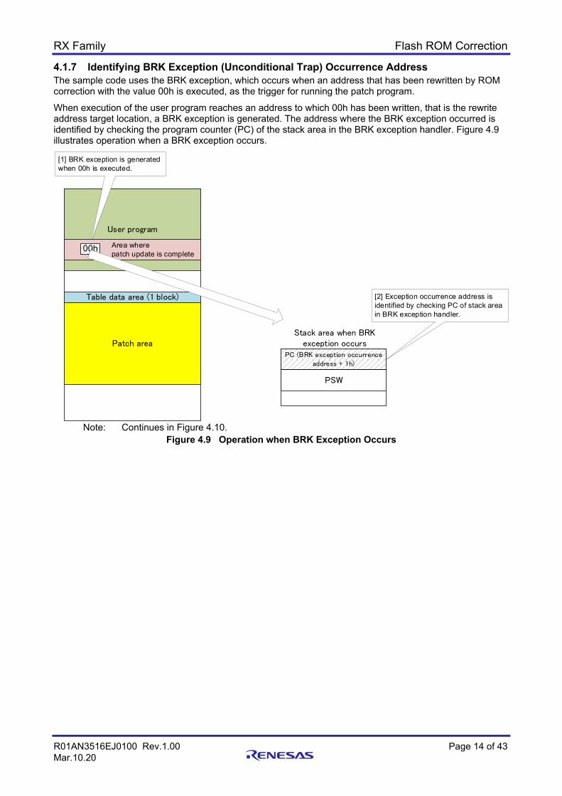
4.1.7 Identifying BRK Exception (Unconditional Trap) Occurrence Address The sample code uses the BRK exception, which occurs when an address that has been rewritten by ROM correction with the value 00h is executed, as the trigger for running the patch program.
When execution of the user program reaches an address to which 00h has been written, that is the rewrite address target location, a BRK exception is generated. The address where the BRK exception occurred is identified by checking the program counter (PC) of the stack area in the BRK exception handler. Figure 4.9 illustrates operation when a BRK exception occurs.
Note: Continues in Figure 4.10. Figure 4.9 Operation when BRK Exception Occurs
User program
Table data area (1 block)
[1] BRK exception is generated when 00h is executed.
PC (BRK exception occurrence address + 1h)
PSW
[2] Exception occurrence address is identified by checking PC of stack area in BRK exception handler.
Stack area when BRK exception occursPatch area
Area where patch update is complete
00h
RX Family Flash ROM Correction
R01AN3516EJ0100 Rev.1.00 Page 15 of 43 Mar.10.20
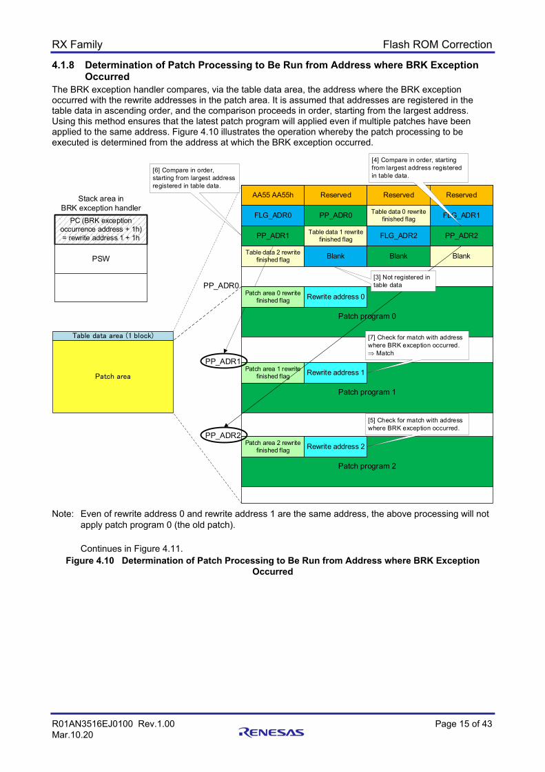
4.1.8 Determination of Patch Processing to Be Run from Address where BRK Exception Occurred
The BRK exception handler compares, via the table data area, the address where the BRK exception occurred with the rewrite addresses in the patch area. It is assumed that addresses are registered in the table data in ascending order, and the comparison proceeds in order, starting from the largest address. Using this method ensures that the latest patch program will applied even if multiple patches have been applied to the same address. Figure 4.10 illustrates the operation whereby the patch processing to be executed is determined from the address at which the BRK exception occurred.
Note: Even of rewrite address 0 and rewrite address 1 are the same address, the above processing will not
apply patch program 0 (the old patch). Continues in Figure 4.11.
Figure 4.10 Determination of Patch Processing to Be Run from Address where BRK Exception Occurred
Table data area (1 block)
Patch area
PC (BRK exception occurrence address + 1h) = rewrite address 1 + 1h
PSW
Stack area in BRK exception handler
AA55 AA55h
FLG_ADR0 PP_ADR0 Table data 0 rewrite finished flag FLG_ADR1
Reserved Reserved Reserved
PP_ADR1 Table data 1 rewrite finished flag FLG_ADR2 PP_ADR2
Table data 2 rewrite finished flag
PP_ADR0
Patch program 0
PP_ADR1
[6] Compare in order, starting from largest address registered in table data.
[4] Compare in order, starting from largest address registered in table data.
PP_ADR2
Patch program 1
Blank Blank Blank
Patch program 2
[7] Check for match with address where BRK exception occurred. ⇒ Match
[5] Check for match with address where BRK exception occurred.
Patch area 1 rewrite finished flag Rewrite address 1
Patch area 0 rewrite finished flag Rewrite address 0
Patch area 2 rewrite finished flag Rewrite address 2
[3] Not registered in table data
RX Family Flash ROM Correction
R01AN3516EJ0100 Rev.1.00 Page 16 of 43 Mar.10.20
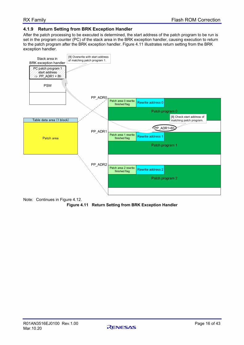
4.1.9 Return Setting from BRK Exception Handler After the patch processing to be executed is determined, the start address of the patch program to be run is set in the program counter (PC) of the stack area in the BRK exception handler, causing execution to return to the patch program after the BRK exception handler. Figure 4.11 illustrates return setting from the BRK exception handler.
Note: Continues in Figure 4.12.
Figure 4.11 Return Setting from BRK Exception Handler
Table data area (1 block)
Patch area
PSW
Stack area in BRK exception handler
PP_ADR0
Patch program 0
PP_ADR1
PP_ADR2
Patch program 1
Patch program 2
Patch area 1 rewrite finished flag Rewrite address 1
PP_ADR1+8h
PC patch program 1 start address
⇒ PP_ADR1 + 8h
[8] Check start address of matching patch program.
[9] Overwrite with start address of matching patch program 1.
Patch area 2 rewrite finished flag Rewrite address 2
Patch area 0 rewrite finished flag Rewrite address 0
RX Family Flash ROM Correction
R01AN3516EJ0100 Rev.1.00 Page 17 of 43 Mar.10.20
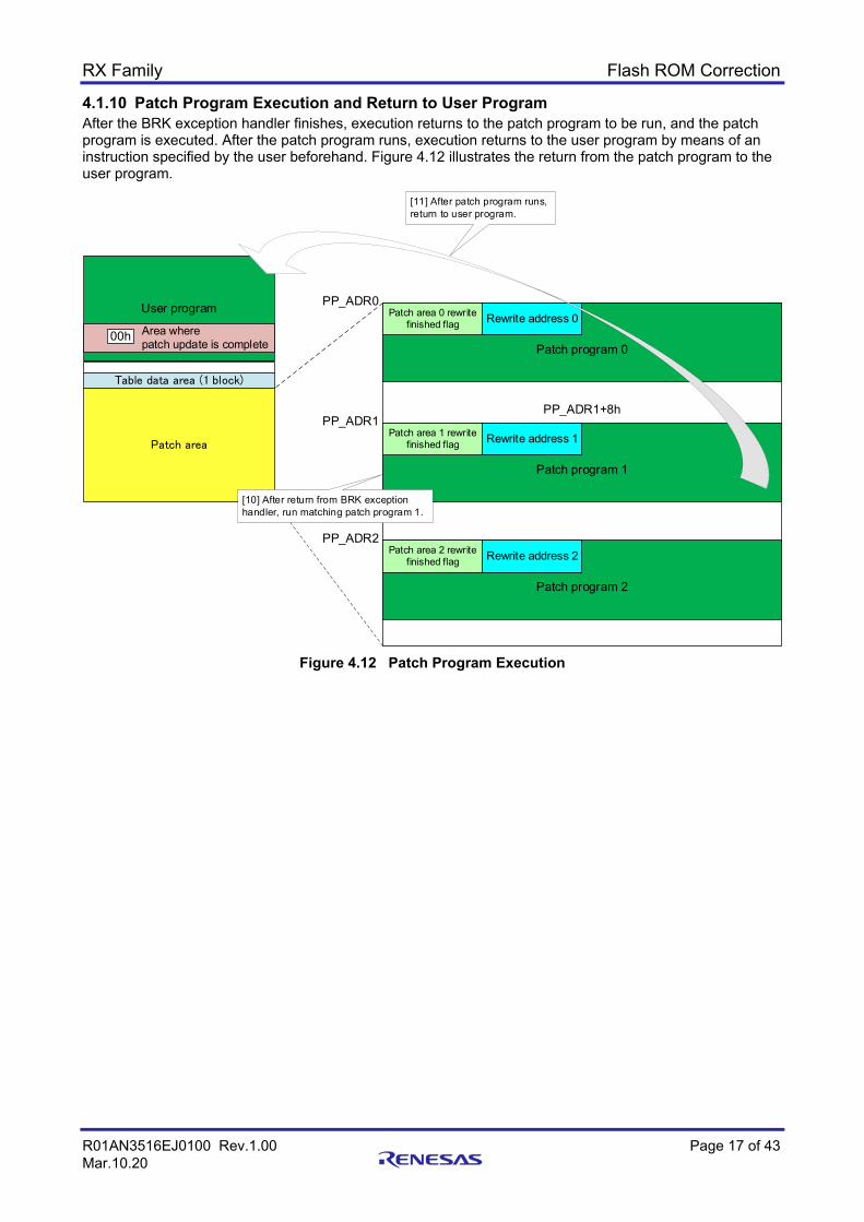
4.1.10 Patch Program Execution and Return to User Program After the BRK exception handler finishes, execution returns to the patch program to be run, and the patch program is executed. After the patch program runs, execution returns to the user program by means of an instruction specified by the user beforehand. Figure 4.12 illustrates the return from the patch program to the user program.
Figure 4.12 Patch Program Execution
Table data area (1 block)
Patch area
PP_ADR0
Patch program 0
PP_ADR1
PP_ADR2
Patch program 1
Patch program 2
Patch area 1 rewrite finished flag Rewrite address 1
PP_ADR1+8h
User program
Area where patch update is complete
00h
[11] After patch program runs, return to user program.
[10] After return from BRK exception handler, run matching patch program 1.
Patch area 0 rewrite finished flag Rewrite address 0
Patch area 2 rewrite finished flag Rewrite address 2
RX Family Flash ROM Correction
R01AN3516EJ0100 Rev.1.00 Page 18 of 43 Mar.10.20
4.2 Required Memory Sizes Table 4.1 lists the required memory sizes.
Table 4.1 Required Memory Sizes
Memory Used Size Remarks ROM 1,028 bytes In r_rom_correct.c module RAM 20 bytes In r_rom_correct.c module Patch work area 1,300 bytes In r_rom_correct.c module
Size depends on capacity of patch application area to be copied. 2,531 bytes Capacity used in r_flash_rx module
Note: The required memory sizes differ depending on the version of the C compiler and the compile options used. Refer to the applicable application notes for the sizes of r_bsp and r_flash_rx.
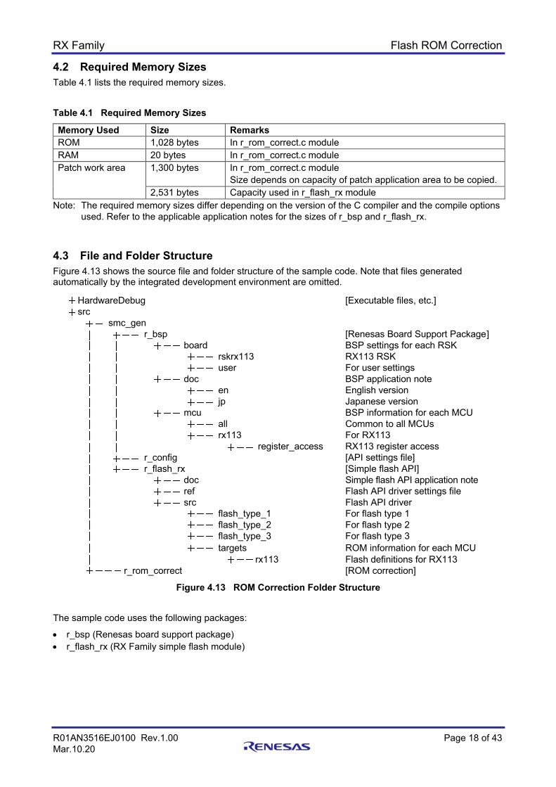
4.3 File and Folder Structure Figure 4.13 shows the source file and folder structure of the sample code. Note that files generated automatically by the integrated development environment are omitted.
HardwareDebug [Executable files, etc.] src
smc_genr_bsp [Renesas Board Support Package]
board BSP settings for each RSKrskrx113 RX113 RSKuser For user settings
doc BSP application noteen English versionjp Japanese version
mcu BSP information for each MCUall Common to all MCUsrx113 For RX113
register_access RX113 register accessr_config [API settings file]r_flash_rx [Simple flash API]
doc Simple flash API application noteref Flash API driver settings filesrc Flash API driver
flash_type_1 For flash type 1flash_type_2 For flash type 2flash_type_3 For flash type 3targets ROM information for each MCU
rx113 Flash definitions for RX113 r_rom_correct [ROM correction]
Figure 4.13 ROM Correction Folder Structure
The sample code uses the following packages:
• r_bsp (Renesas board support package) • r_flash_rx (RX Family simple flash module)
RX Family Flash ROM Correction
R01AN3516EJ0100 Rev.1.00 Page 19 of 43 Mar.10.20
4.3.1 src Folder This folder contains a sample source file and header file used by the ROM correction program.
Table 4.2 Sample Files Used
File Name Description Notes main.c Source file of main routine main.h Header file of main routine
4.3.2 src\r_bsp Folder This folder contains the source files and header files of the Renesas Board Support Package module. For details, refer to the RX Family Board Support Package Module application note.
4.3.3 src\r_config Folder Table 4.3 lists the files in the folder containing the setting files for the target MCU.
Table 4.3 Header Files
File Name Description Notes r_bsp_config.h BSP settings header file For RSK RX113 r_flash_rx_config.h Flash write settings file
4.3.4 src\r_flash_rx Folder This folder contains the source files and header files of the flash FIT module. For details, refer to the Flash Module Firmware Integration Technology application note.
4.3.5 src\r_rom_correct Folder This folder contains the source file and header file of the ROM correction program.
Table 4.4 ROM Correction
File Name Description Notes r_rom_correct.c ROM correction source file r_rom_correct.h ROM correction header file
RX Family Flash ROM Correction
R01AN3516EJ0100 Rev.1.00 Page 20 of 43 Mar.10.20
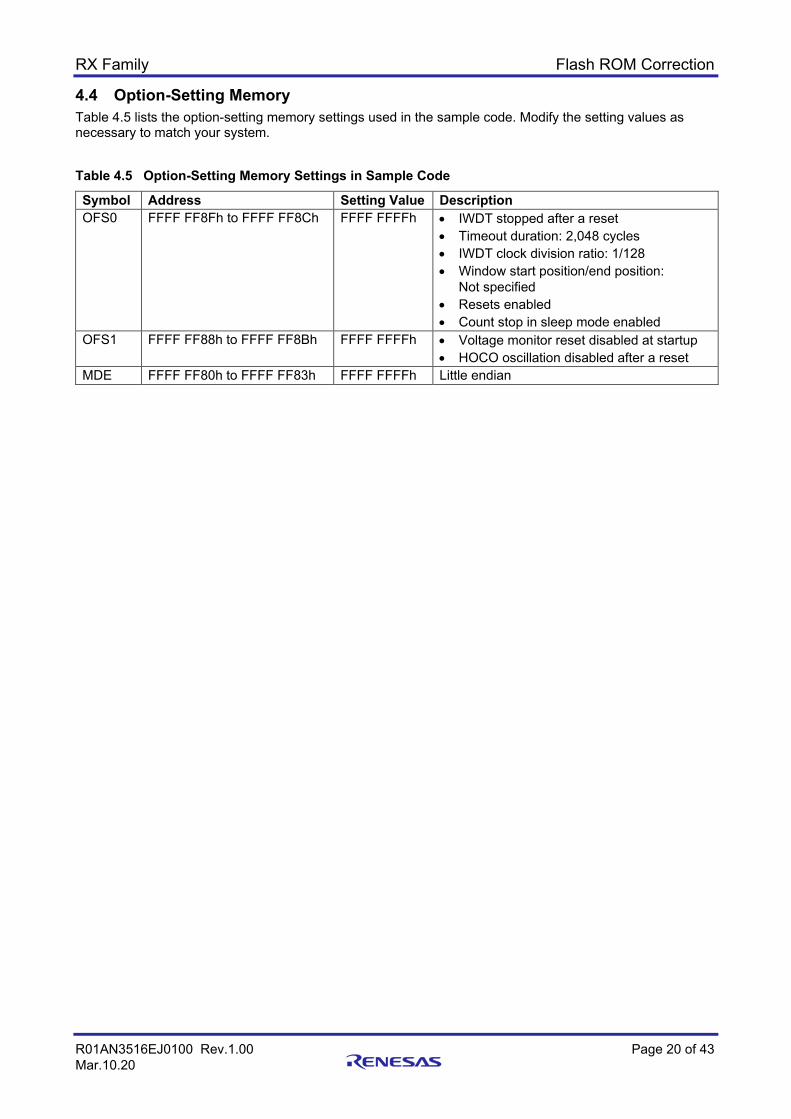
4.4 Option-Setting Memory Table 4.5 lists the option-setting memory settings used in the sample code. Modify the setting values as necessary to match your system.
Table 4.5 Option-Setting Memory Settings in Sample Code
Symbol Address Setting Value Description OFS0 FFFF FF8Fh to FFFF FF8Ch FFFF FFFFh • IWDT stopped after a reset
• Timeout duration: 2,048 cycles • IWDT clock division ratio: 1/128 • Window start position/end position:
Not specified • Resets enabled • Count stop in sleep mode enabled
OFS1 FFFF FF88h to FFFF FF8Bh FFFF FFFFh • Voltage monitor reset disabled at startup • HOCO oscillation disabled after a reset
MDE FFFF FF80h to FFFF FF83h FFFF FFFFh Little endian
RX Family Flash ROM Correction
R01AN3516EJ0100 Rev.1.00 Page 21 of 43 Mar.10.20
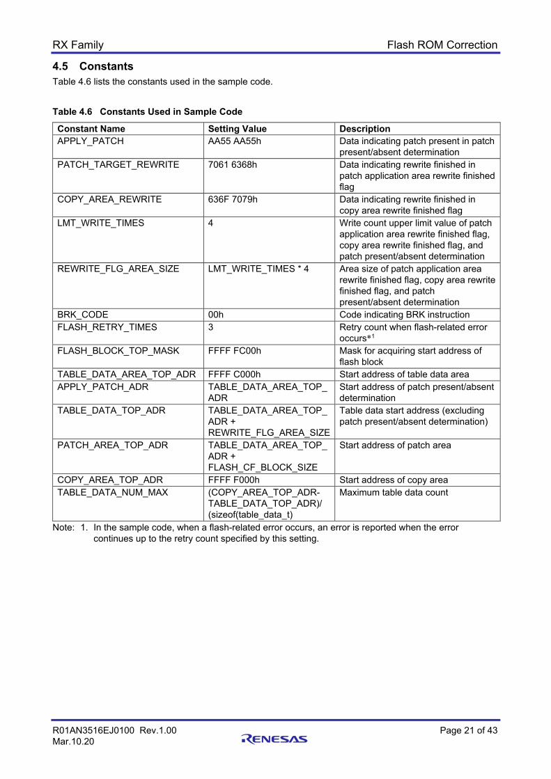
4.5 Constants Table 4.6 lists the constants used in the sample code.
Table 4.6 Constants Used in Sample Code
Constant Name Setting Value Description APPLY_PATCH AA55 AA55h Data indicating patch present in patch
present/absent determination PATCH_TARGET_REWRITE 7061 6368h Data indicating rewrite finished in
patch application area rewrite finished flag
COPY_AREA_REWRITE 636F 7079h Data indicating rewrite finished in copy area rewrite finished flag
LMT_WRITE_TIMES 4 Write count upper limit value of patch application area rewrite finished flag, copy area rewrite finished flag, and patch present/absent determination
REWRITE_FLG_AREA_SIZE LMT_WRITE_TIMES * 4 Area size of patch application area rewrite finished flag, copy area rewrite finished flag, and patch present/absent determination
BRK_CODE 00h Code indicating BRK instruction FLASH_RETRY_TIMES 3 Retry count when flash-related error
occurs*1 FLASH_BLOCK_TOP_MASK FFFF FC00h Mask for acquiring start address of
flash block TABLE_DATA_AREA_TOP_ADR FFFF C000h Start address of table data area APPLY_PATCH_ADR TABLE_DATA_AREA_TOP_
ADR Start address of patch present/absent determination
TABLE_DATA_TOP_ADR TABLE_DATA_AREA_TOP_ADR + REWRITE_FLG_AREA_SIZE
Table data start address (excluding patch present/absent determination)
PATCH_AREA_TOP_ADR TABLE_DATA_AREA_TOP_ADR + FLASH_CF_BLOCK_SIZE
Start address of patch area
COPY_AREA_TOP_ADR FFFF F000h Start address of copy area TABLE_DATA_NUM_MAX (COPY_AREA_TOP_ADR-
TABLE_DATA_TOP_ADR)/ (sizeof(table_data_t)
Maximum table data count
Note: 1. In the sample code, when a flash-related error occurs, an error is reported when the error continues up to the retry count specified by this setting.
RX Family Flash ROM Correction
R01AN3516EJ0100 Rev.1.00 Page 22 of 43 Mar.10.20
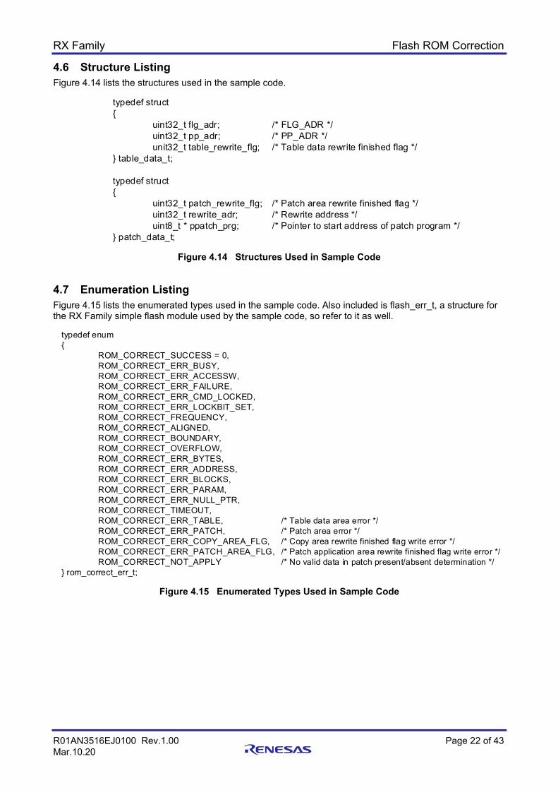
4.6 Structure Listing Figure 4.14 lists the structures used in the sample code.
Figure 4.14 Structures Used in Sample Code
4.7 Enumeration Listing Figure 4.15 lists the enumerated types used in the sample code. Also included is flash_err_t, a structure for the RX Family simple flash module used by the sample code, so refer to it as well.
Figure 4.15 Enumerated Types Used in Sample Code
typedef struct{
uint32_t flg_adr; /* FLG_ADR */uint32_t pp_adr; /* PP_ADR */unit32_t table_rewrite_flg; /* Table data rewrite finished flag */
} table_data_t;
typedef struct{
uint32_t patch_rewrite_flg; /* Patch area rewrite finished flag */uint32_t rewrite_adr; /* Rewrite address */uint8_t * ppatch_prg; /* Pointer to start address of patch program */
} patch_data_t;
typedef enum{
ROM_CORRECT_SUCCESS = 0,ROM_CORRECT_ERR_BUSY,ROM_CORRECT_ERR_ACCESSW,ROM_CORRECT_ERR_FAILURE,ROM_CORRECT_ERR_CMD_LOCKED,ROM_CORRECT_ERR_LOCKBIT_SET,ROM_CORRECT_FREQUENCY,ROM_CORRECT_ALIGNED,ROM_CORRECT_BOUNDARY,ROM_CORRECT_OVERFLOW,ROM_CORRECT_ERR_BYTES,ROM_CORRECT_ERR_ADDRESS,ROM_CORRECT_ERR_BLOCKS,ROM_CORRECT_ERR_PARAM,ROM_CORRECT_ERR_NULL_PTR,ROM_CORRECT_TIMEOUT,ROM_CORRECT_ERR_TABLE, /* Table data area error */ROM_CORRECT_ERR_PATCH, /* Patch area error */ROM_CORRECT_ERR_COPY_AREA_FLG, /* Copy area rewrite finished flag write error */ROM_CORRECT_ERR_PATCH_AREA_FLG, /* Patch application area rewrite finished flag write error */ROM_CORRECT_NOT_APPLY /* No valid data in patch present/absent determination */
} rom_correct_err_t;
RX Family Flash ROM Correction
R01AN3516EJ0100 Rev.1.00 Page 23 of 43 Mar.10.20
4.8 Variables Table 4.7 lists the variables used in the sample code.
Table 4.7 static Type Variables
Type Variable Name Description Used by Function static uint8_t table_data_num Table data registration count • R_ROM_Correct
• setting_patch
4.9 Functions Table 4.8 lists the functions used in the sample code.
Table 4.8 Functions
Function Name Description R_ROM_Correct ROM correction processing R_ROM_MakePatch Go to applicable patch program (BRK exception handler) get_brk_address Get BRK exception occurrence address set_return_adr Set return address to corresponding patch program chk_apply_patch Patch present/absent determination processing setting_patch Set patch to register chk_patch Check patch to register chk_table_data Check table data chk_patch_area Check patch area chk_rewrite_patch_target_area Check patch application area rewrite rewrite_patch_target_area Patch application area rewrite processing chk_rewrite_copy_area Check copy area rewrite rewrite_copy_area Copy area rewrite processing rewrite_brk_code Rewrite patch application area with BRK instruction call_R_FLASH_Open Flash FIT module initialization, including retry in case of error call_R_FLASH_Erase Erase flash, including retry in case of error call_R_FLASH_BlankCheck Flash blank check, including retry in case of error call_R_FLASH_Write Write to flash, including retry in case of error
RX Family Flash ROM Correction
R01AN3516EJ0100 Rev.1.00 Page 24 of 43 Mar.10.20
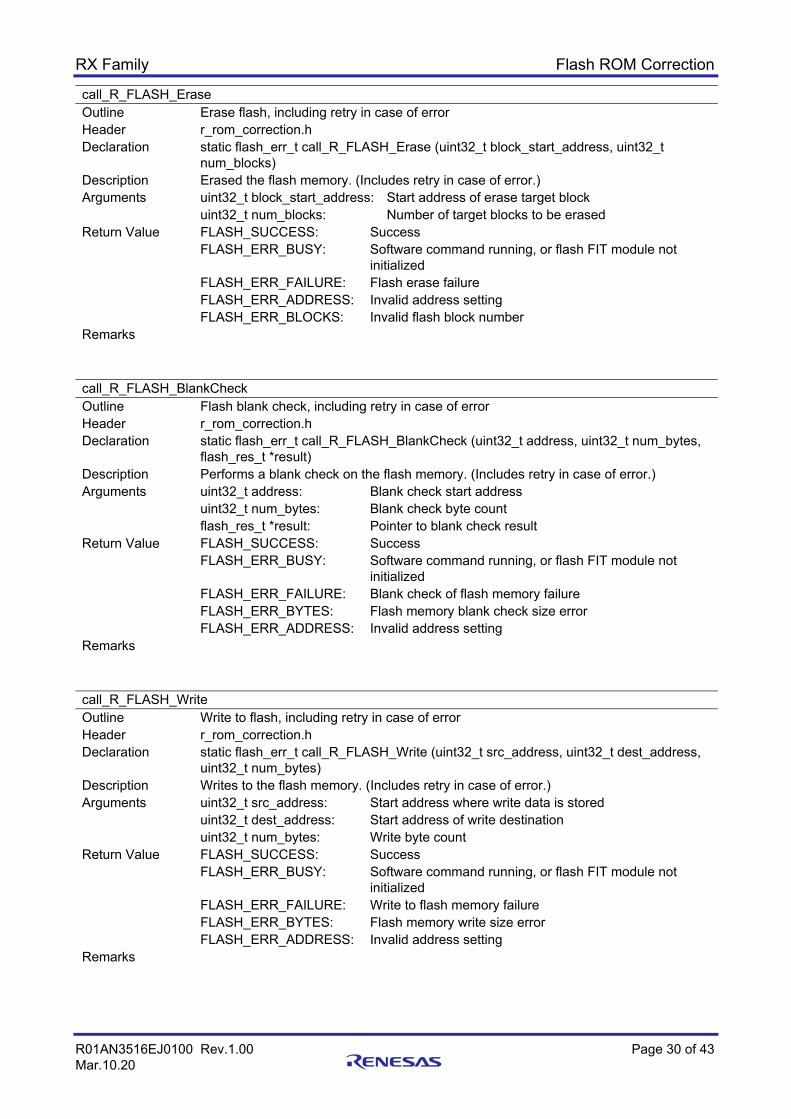
4.10 Function Specifications The following tables list the sample code function specifications.
R_ROM_Correct Outline ROM correction function Header r_rom_correct.h Declaration rom_correct_err_t R_ROM_Correct (void) Description ROM correction processing Arguments None Return Value ROM correction setting result
ROM_CORRECT_SUCCESS: Success ROM_CORRECT_ERR_BUSY: Software command running, or flash FIT module
not initialized ROM_CORRECT_ERR_FAILURE: Flash blank check, erase, or write failure ROM_CORRECT_ERR_BYTES: Flash write or blank check size error ROM_CORRECT_ERR_ADDRESS: Invalid address setting ROM_CORRECT_ERR_BLOCKS: Invalid flash block number ROM_CORRECT_ERR_TABLE: Table data area setting error ROM_CORRECT_ERR_PATCH: Patch area setting error ROM_CORRECT_ERR_WR_COPY_FLAG:
Copy area rewrite finished flag write error ROM_CORRECT_ERR_WR_PATCH_FLAG:
Patch application area rewrite finished flag write error
ROM_CORRECT_NOT_APPLY: No valid data in patch present/absent determination
Remarks Except for ROM_CORRECT_NOT_APPLY, the last registered table data setting result is sent as the return value. If setting result information is needed for each table data item, register each table data item and patch area individually.
R_ROM_MakePatch Outline Go to applicable patch program (BRK exception handler) Header r_rom_correction.h Declaration void R_ROM_MakePatch (void) Description Determines the applicable patch program from the address at which the BRK exception
occurred and transitions to it. Arguments None Return Value None Remarks This function is a BRK exception handler.
RX Family Flash ROM Correction
R01AN3516EJ0100 Rev.1.00 Page 25 of 43 Mar.10.20
get_brk_address Outline Get BRK exception occurrence address Header r_rom_correction.h Declaration uint32_t get_brk_address (void) Description Gets the address at which the BRK exception occurred. Arguments None Return Value Address where BRK exception occurred + 1 Remarks This function is declared in #pragma inline_asm.
If the R_ROM_MakePatch function is altered to change the capacity of the stack where the data is saved, this function should be modified to match.
Set_return_adr Outline Set return address to corresponding patch program Header r_rom_correction.h Declaration uint32_t set_return_adr (uint32_t return_adr) Description Sets the address to return to from the BRK exception handler. Arguments uint32_t return_adr: State address of applicable patch program Return Value None Remarks This function is declared in #pragma inline_asm.
If the R_ROM_MakePatch function is altered to change the capacity of the stack where the data is saved, this function should be modified to match.
chk_apply_patch Outline Patch present/absent determination processing Header r_rom_correction.h Declaration static rom_correct_err_t chk_apply_patch (void) Description Checks the patch present/absent determination. Arguments None Return Value Patch present/absent checking result
ROM_CORRECT_SUCCESS: Patch present ROM_CORRECT_NOT_APPLY: No valid data in patch present/absent
determination Remarks
RX Family Flash ROM Correction
R01AN3516EJ0100 Rev.1.00 Page 26 of 43 Mar.10.20
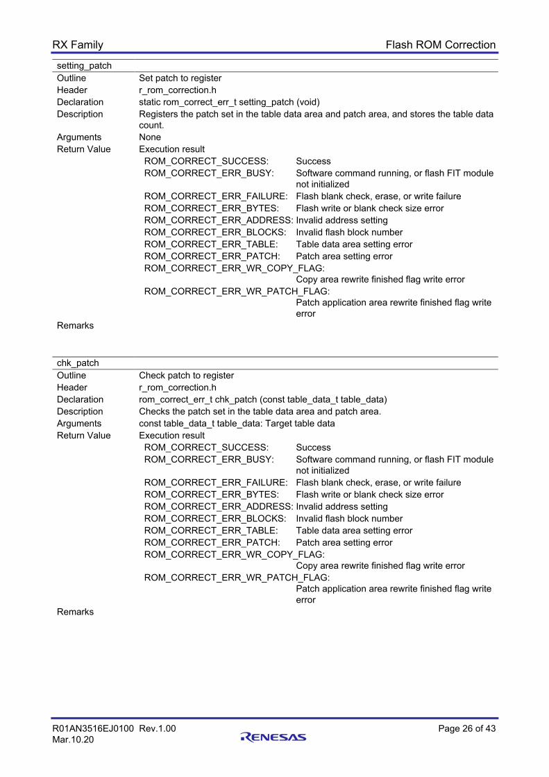
setting_patch Outline Set patch to register Header r_rom_correction.h Declaration static rom_correct_err_t setting_patch (void) Description Registers the patch set in the table data area and patch area, and stores the table data
count. Arguments None Return Value Execution result
ROM_CORRECT_SUCCESS: Success ROM_CORRECT_ERR_BUSY: Software command running, or flash FIT module
not initialized ROM_CORRECT_ERR_FAILURE: Flash blank check, erase, or write failure ROM_CORRECT_ERR_BYTES: Flash write or blank check size error ROM_CORRECT_ERR_ADDRESS: Invalid address setting ROM_CORRECT_ERR_BLOCKS: Invalid flash block number ROM_CORRECT_ERR_TABLE: Table data area setting error ROM_CORRECT_ERR_PATCH: Patch area setting error ROM_CORRECT_ERR_WR_COPY_FLAG:
Copy area rewrite finished flag write error ROM_CORRECT_ERR_WR_PATCH_FLAG:
Patch application area rewrite finished flag write error
Remarks chk_patch Outline Check patch to register Header r_rom_correction.h Declaration rom_correct_err_t chk_patch (const table_data_t table_data) Description Checks the patch set in the table data area and patch area. Arguments const table_data_t table_data: Target table data Return Value Execution result
ROM_CORRECT_SUCCESS: Success ROM_CORRECT_ERR_BUSY: Software command running, or flash FIT module
not initialized ROM_CORRECT_ERR_FAILURE: Flash blank check, erase, or write failure ROM_CORRECT_ERR_BYTES: Flash write or blank check size error ROM_CORRECT_ERR_ADDRESS: Invalid address setting ROM_CORRECT_ERR_BLOCKS: Invalid flash block number ROM_CORRECT_ERR_TABLE: Table data area setting error ROM_CORRECT_ERR_PATCH: Patch area setting error ROM_CORRECT_ERR_WR_COPY_FLAG:
Copy area rewrite finished flag write error ROM_CORRECT_ERR_WR_PATCH_FLAG:
Patch application area rewrite finished flag write error
Remarks
RX Family Flash ROM Correction
R01AN3516EJ0100 Rev.1.00 Page 27 of 43 Mar.10.20
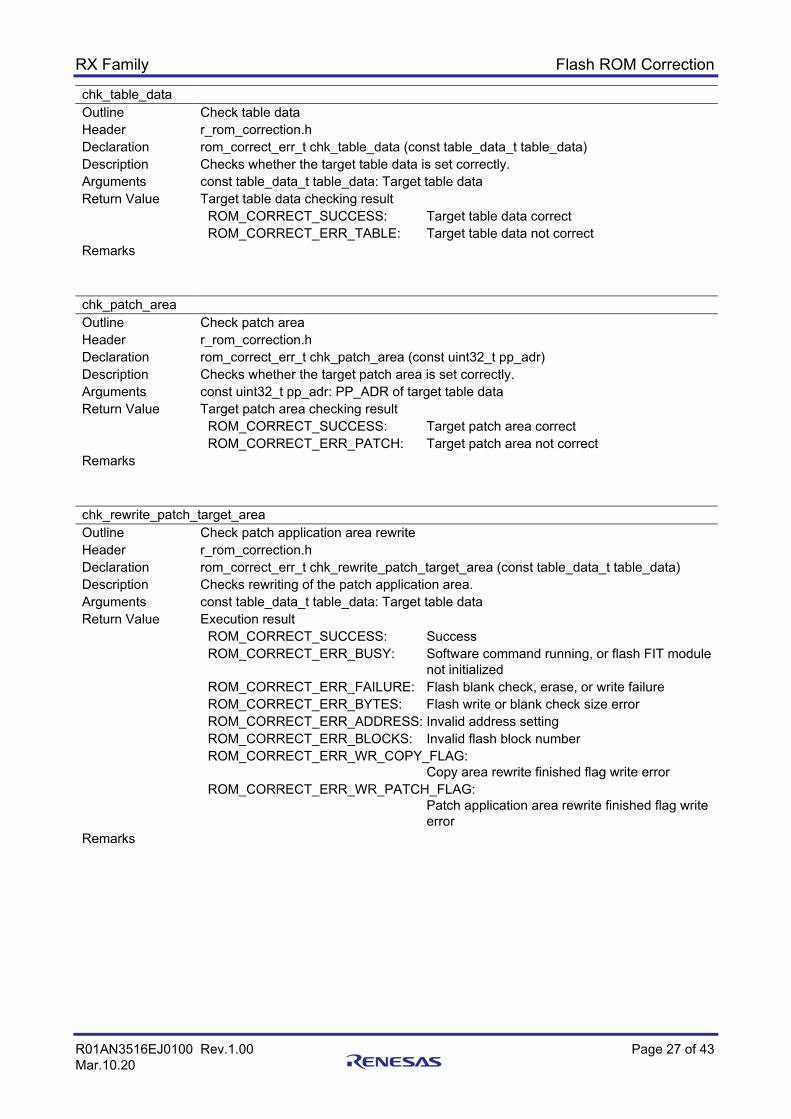
chk_table_data Outline Check table data Header r_rom_correction.h Declaration rom_correct_err_t chk_table_data (const table_data_t table_data) Description Checks whether the target table data is set correctly. Arguments const table_data_t table_data: Target table data Return Value Target table data checking result
ROM_CORRECT_SUCCESS: Target table data correct ROM_CORRECT_ERR_TABLE: Target table data not correct
Remarks chk_patch_area Outline Check patch area Header r_rom_correction.h Declaration rom_correct_err_t chk_patch_area (const uint32_t pp_adr) Description Checks whether the target patch area is set correctly. Arguments const uint32_t pp_adr: PP_ADR of target table data Return Value Target patch area checking result
ROM_CORRECT_SUCCESS: Target patch area correct ROM_CORRECT_ERR_PATCH: Target patch area not correct
Remarks chk_rewrite_patch_target_area Outline Check patch application area rewrite Header r_rom_correction.h Declaration rom_correct_err_t chk_rewrite_patch_target_area (const table_data_t table_data) Description Checks rewriting of the patch application area. Arguments const table_data_t table_data: Target table data Return Value Execution result
ROM_CORRECT_SUCCESS: Success ROM_CORRECT_ERR_BUSY: Software command running, or flash FIT module
not initialized ROM_CORRECT_ERR_FAILURE: Flash blank check, erase, or write failure ROM_CORRECT_ERR_BYTES: Flash write or blank check size error ROM_CORRECT_ERR_ADDRESS: Invalid address setting ROM_CORRECT_ERR_BLOCKS: Invalid flash block number ROM_CORRECT_ERR_WR_COPY_FLAG:
Copy area rewrite finished flag write error ROM_CORRECT_ERR_WR_PATCH_FLAG:
Patch application area rewrite finished flag write error
Remarks
RX Family Flash ROM Correction
R01AN3516EJ0100 Rev.1.00 Page 28 of 43 Mar.10.20
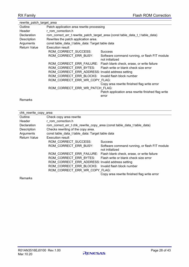
rewrite_patch_target_area Outline Patch application area rewrite processing Header r_rom_correction.h Declaration rom_correct_err_t rewrite_patch_target_area (const table_data_t_t table_data) Description Rewrites the patch application area. Arguments const table_data_t table_data: Target table data Return Value Execution result
ROM_CORRECT_SUCCESS: Success ROM_CORRECT_ERR_BUSY: Software command running, or flash FIT module
not initialized ROM_CORRECT_ERR_FAILURE: Flash blank check, erase, or write failure ROM_CORRECT_ERR_BYTES: Flash write or blank check size error ROM_CORRECT_ERR_ADDRESS: Invalid address setting ROM_CORRECT_ERR_BLOCKS: Invalid flash block number ROM_CORRECT_ERR_WR_COPY_FLAG:
Copy area rewrite finished flag write error ROM_CORRECT_ERR_WR_PATCH_FLAG:
Patch application area rewrite finished flag write error
Remarks chk_rewrite_copy_area Outline Check copy area rewrite Header r_rom_correction.h Declaration rom_correct_err_t chk_rewrite_copy_area (const table_data_t table_data) Description Checks rewriting of the copy area. Arguments const table_data_t table_data: Target table data Return Value Execution result
ROM_CORRECT_SUCCESS: Success ROM_CORRECT_ERR_BUSY: Software command running, or flash FIT module
not initialized ROM_CORRECT_ERR_FAILURE: Flash blank check, erase, or write failure ROM_CORRECT_ERR_BYTES: Flash write or blank check size error ROM_CORRECT_ERR_ADDRESS: Invalid address setting ROM_CORRECT_ERR_BLOCKS: Invalid flash block number ROM_CORRECT_ERR_WR_COPY_FLAG:
Copy area rewrite finished flag write error Remarks
RX Family Flash ROM Correction
R01AN3516EJ0100 Rev.1.00 Page 29 of 43 Mar.10.20
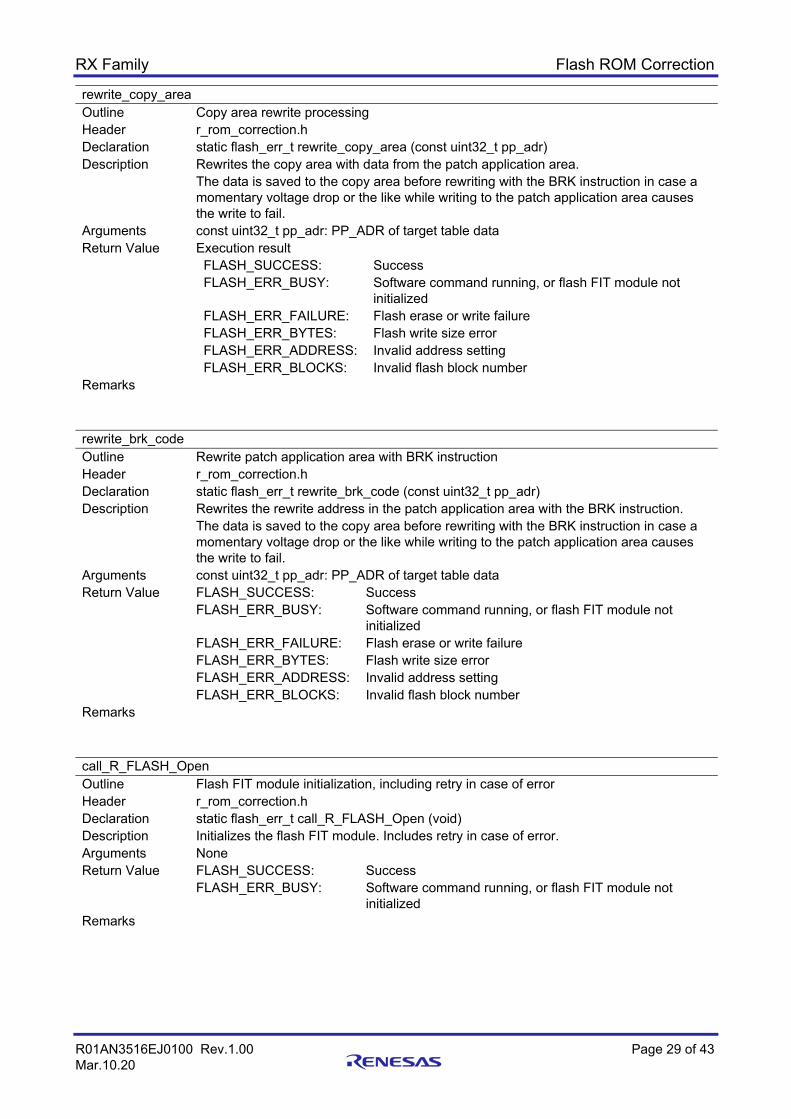
rewrite_copy_area Outline Copy area rewrite processing Header r_rom_correction.h Declaration static flash_err_t rewrite_copy_area (const uint32_t pp_adr) Description Rewrites the copy area with data from the patch application area.
The data is saved to the copy area before rewriting with the BRK instruction in case a momentary voltage drop or the like while writing to the patch application area causes the write to fail.
Arguments const uint32_t pp_adr: PP_ADR of target table data Return Value Execution result
FLASH_SUCCESS: Success FLASH_ERR_BUSY: Software command running, or flash FIT module not
initialized FLASH_ERR_FAILURE: Flash erase or write failure FLASH_ERR_BYTES: Flash write size error FLASH_ERR_ADDRESS: Invalid address setting FLASH_ERR_BLOCKS: Invalid flash block number
Remarks rewrite_brk_code Outline Rewrite patch application area with BRK instruction Header r_rom_correction.h Declaration static flash_err_t rewrite_brk_code (const uint32_t pp_adr) Description Rewrites the rewrite address in the patch application area with the BRK instruction.
The data is saved to the copy area before rewriting with the BRK instruction in case a momentary voltage drop or the like while writing to the patch application area causes the write to fail.
Arguments const uint32_t pp_adr: PP_ADR of target table data Return Value FLASH_SUCCESS: Success
FLASH_ERR_BUSY: Software command running, or flash FIT module not initialized
FLASH_ERR_FAILURE: Flash erase or write failure FLASH_ERR_BYTES: Flash write size error FLASH_ERR_ADDRESS: Invalid address setting FLASH_ERR_BLOCKS: Invalid flash block number
Remarks call_R_FLASH_Open Outline Flash FIT module initialization, including retry in case of error Header r_rom_correction.h Declaration static flash_err_t call_R_FLASH_Open (void) Description Initializes the flash FIT module. Includes retry in case of error. Arguments None Return Value FLASH_SUCCESS: Success
FLASH_ERR_BUSY: Software command running, or flash FIT module not initialized
Remarks
RX Family Flash ROM Correction
R01AN3516EJ0100 Rev.1.00 Page 30 of 43 Mar.10.20
call_R_FLASH_Erase Outline Erase flash, including retry in case of error Header r_rom_correction.h Declaration static flash_err_t call_R_FLASH_Erase (uint32_t block_start_address, uint32_t
num_blocks) Description Erased the flash memory. (Includes retry in case of error.) Arguments uint32_t block_start_address: Start address of erase target block
uint32_t num_blocks: Number of target blocks to be erased Return Value FLASH_SUCCESS: Success
FLASH_ERR_BUSY: Software command running, or flash FIT module not initialized
FLASH_ERR_FAILURE: Flash erase failure FLASH_ERR_ADDRESS: Invalid address setting FLASH_ERR_BLOCKS: Invalid flash block number
Remarks call_R_FLASH_BlankCheck Outline Flash blank check, including retry in case of error Header r_rom_correction.h Declaration static flash_err_t call_R_FLASH_BlankCheck (uint32_t address, uint32_t num_bytes,
flash_res_t *result) Description Performs a blank check on the flash memory. (Includes retry in case of error.) Arguments uint32_t address: Blank check start address
uint32_t num_bytes: Blank check byte count flash_res_t *result: Pointer to blank check result
Return Value FLASH_SUCCESS: Success FLASH_ERR_BUSY: Software command running, or flash FIT module not
initialized FLASH_ERR_FAILURE: Blank check of flash memory failure FLASH_ERR_BYTES: Flash memory blank check size error FLASH_ERR_ADDRESS: Invalid address setting
Remarks call_R_FLASH_Write Outline Write to flash, including retry in case of error Header r_rom_correction.h Declaration static flash_err_t call_R_FLASH_Write (uint32_t src_address, uint32_t dest_address,
uint32_t num_bytes) Description Writes to the flash memory. (Includes retry in case of error.) Arguments uint32_t src_address: Start address where write data is stored
uint32_t dest_address: Start address of write destination uint32_t num_bytes: Write byte count
Return Value FLASH_SUCCESS: Success FLASH_ERR_BUSY: Software command running, or flash FIT module not
initialized FLASH_ERR_FAILURE: Write to flash memory failure FLASH_ERR_BYTES: Flash memory write size error FLASH_ERR_ADDRESS: Invalid address setting
Remarks
RX Family Flash ROM Correction
R01AN3516EJ0100 Rev.1.00 Page 31 of 43 Mar.10.20
5. Precautions 5.1 Precautions When Using This Application Note • The user should write data to the table data area and patch area beforehand using self-rewrite in P/E
mode, or the like. Note that when using a serial programmer it is not possible to use a boot program to write the data.
• When writing data to the table data area and patch area, do not write FFh to the reserved areas and empty areas.
• The user’s R_ROM_Correct function sends the last setting result registered in the table data as its return value. If setting result information is needed for each table data item, register each table data item and patch area individually.
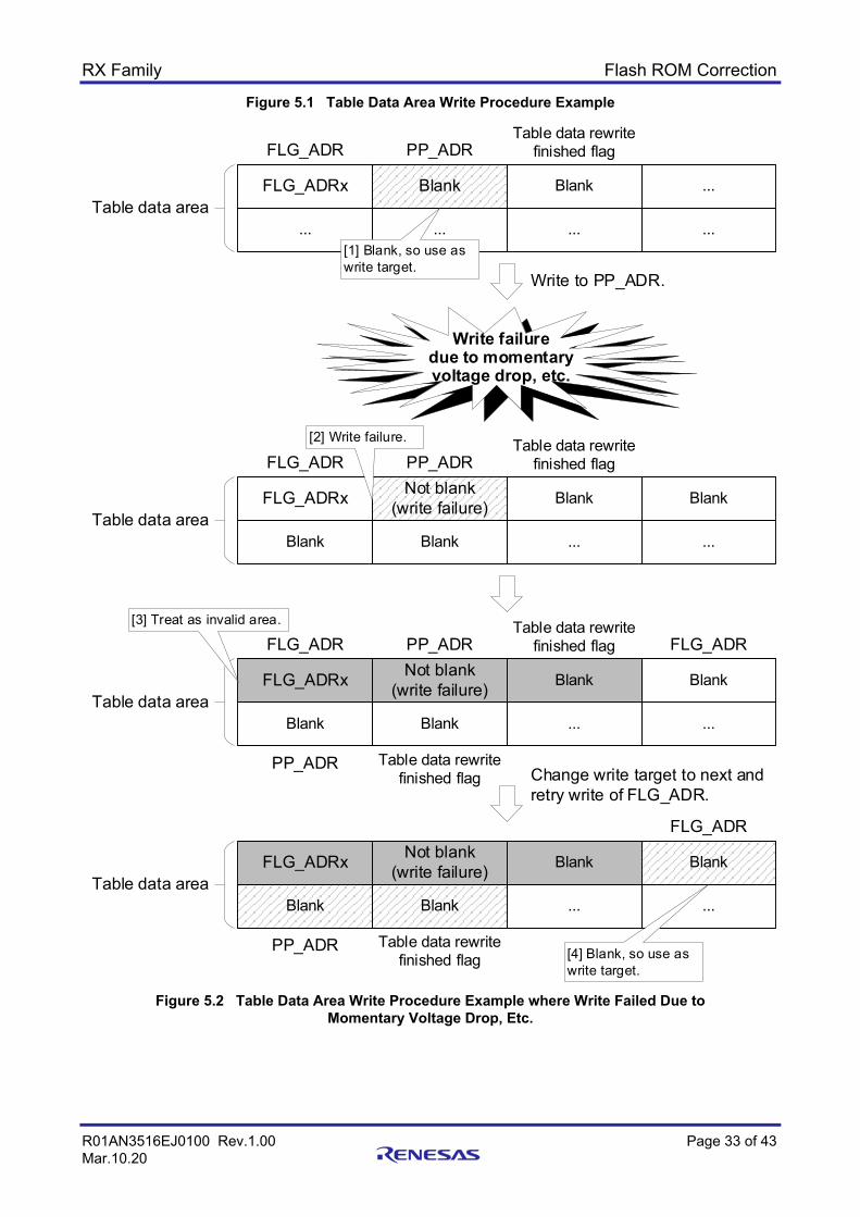
5.2 Table Data Area and Patch Area Write Procedure Examples Examples of the procedures for writing to the table data area and patch area implemented by the user are described below. Figure 5.1 shows a table data area write procedure example. Figure 5.2 shows a write procedure example where the write failed due to a momentary voltage drop or the like. Note that the user should make sure to run a blank check before writing data.
1. Only when applying a patch for the first time, write AA55 AA55h to the patch present/absent determination in the table data area. It is not necessary to write AA55 AA55h to the patch present/absent determination when applying a patch the second or subsequent times.
2. Write data to the table data area and to the patch area, in that order.
2-1. After writing to the table data area, write the table data rewrite finished flag (inverted value of FLG_ADR).
2-2. After writing to the patch area, write the patch area rewrite finished flag (inverted value of rewrite address).
2-3. Repeat steps 2-1 and 2-2 to write additional patch data. If the write fails due to a momentary voltage drop or the like, retry the write in the next empty area. Note that the table data consists of 12-byte sets comprising FLG_ADR, PP_ADR, and the table data rewrite finished flag. For FLG_ADR(m), add 0Ch to the FLG_ADR(m − 1) write address.
Note: Since PP_ADR changes when a write to the patch area fails, you will need to redo the procedure from
step 2-1. Also, do not perform an erase if a write fails; write the data to the next area.
RX Family Flash ROM Correction
R01AN3516EJ0100 Rev.1.00 Page 32 of 43 Mar.10.20
Blank Blank Blank ...
... ... ... ...Table data area
FLG_ADR PP_ADRTable data rewrite
finished flag
FLG_ADRx Blank Blank ...
... ... ... ...Table data area
FLG_ADR PP_ADRTable data rewrite
finished flag
[1] Blank, so use as write target.
FLG_ADRx PP_ADRx Blank ...
... ... ... ...Table data area
FLG_ADR PP_ADRTable data rewrite
finished flag
FLG_ADRx Blank Blank ...
... ... ... ...Table data area
FLG_ADR PP_ADRTable data rewrite
finished flag
[3] Blank, so use as write target.
Write to PP_ADR.
FLG_ADRx PP_ADRx Table data x rewrite finished flag ...
... ... ... ...Table data area
FLG_ADR PP_ADRTable data rewrite
finished flag
FLG_ADRx PP_ADRx Blank ...
... ... ... ...Table data area
FLG_ADR PP_ADRTable data rewrite
finished flag[5] Blank, so use as write target.
[2] Write FLG_ADRx
[4] Write PP_ADRx
[6] Write table data x rewrite finished flag.
RX Family Flash ROM Correction
R01AN3516EJ0100 Rev.1.00 Page 33 of 43 Mar.10.20
Figure 5.1 Table Data Area Write Procedure Example
Figure 5.2 Table Data Area Write Procedure Example where Write Failed Due to
Momentary Voltage Drop, Etc.
FLG_ADRx Not blank (write failure) Blank Blank
Blank Blank ... ...Table data area
FLG_ADR PP_ADRTable data rewrite
finished flag
FLG_ADRx Blank Blank ...
... ... ... ...Table data area
FLG_ADR PP_ADRTable data rewrite
finished flag
[1] Blank, so use as write target.
Write to PP_ADR.
FLG_ADRx Not blank (write failure) Blank Blank
Blank Blank ... ...Table data area
FLG_ADR PP_ADRTable data rewrite
finished flag
Write failure due to momentary voltage drop, etc.
FLG_ADR
PP_ADR Table data rewrite finished flag
[2] Write failure.
[3] Treat as invalid area.
FLG_ADRx Not blank (write failure) Blank Blank
Blank Blank ... ...Table data area
FLG_ADR
PP_ADR Table data rewrite finished flag
Change write target to next and retry write of FLG_ADR.
[4] Blank, so use as write target.
RX Family Flash ROM Correction
R01AN3516EJ0100 Rev.1.00 Page 34 of 43 Mar.10.20
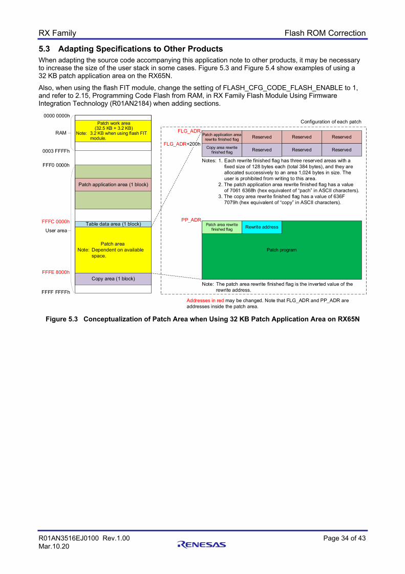
5.3 Adapting Specifications to Other Products When adapting the source code accompanying this application note to other products, it may be necessary to increase the size of the user stack in some cases. Figure 5.3 and Figure 5.4 show examples of using a 32 KB patch application area on the RX65N.
Also, when using the flash FIT module, change the setting of FLASH_CFG_CODE_FLASH_ENABLE to 1, and refer to 2.15, Programming Code Flash from RAM, in RX Family Flash Module Using Firmware Integration Technology (R01AN2184) when adding sections.
Figure 5.3 Conceptualization of Patch Area when Using 32 KB Patch Application Area on RX65N
Patch work area (32.5 KB + 3.2 KB)
Note: 3.2 KB when using flash FIT module.
Patch application area (1 block)
Table data area (1 block)
Patch area Note: Dependent on available
space.
RAM
User area
0000 0000h
0003 FFFFh
FFF0 0000h
FFFF FFFFh
Patch application area rewrite finished flag
Patch program
FLG_ADR
FLG_ADR+200h
PP_ADR
Copy area (1 block)
Reserved Reserved Reserved
FFFE 8000h
Patch area rewrite finished flag Rewrite address
Copy area rewrite finished flag Reserved Reserved Reserved
Notes: 1. Each rewrite finished flag has three reserved areas with a fixed size of 128 bytes each (total 384 bytes), and they are allocated successively to an area 1,024 bytes in size. The user is prohibited from writing to this area.
2. The patch application area rewrite finished flag has a value of 7061 6368h (hex equivalent of “pach” in ASCII characters).
3. The copy area rewrite finished flag has a value of 636F 7079h (hex equivalent of “copy” in ASCII characters).
Configuration of each patch
Note: The patch area rewrite finished flag is the inverted value of the rewrite address.
Addresses in red may be changed. Note that FLG_ADR and PP_ADR are addresses inside the patch area.
FFFC 0000h
RX Family Flash ROM Correction
R01AN3516EJ0100 Rev.1.00 Page 35 of 43 Mar.10.20
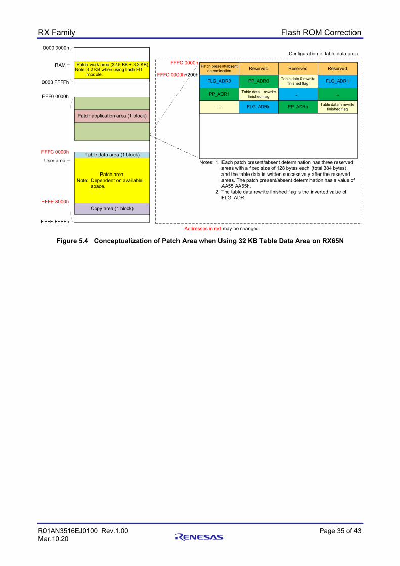
Figure 5.4 Conceptualization of Patch Area when Using 32 KB Table Data Area on RX65N
Patch present/absent determination
FLG_ADR0 PP_ADR0 Table data 0 rewrite finished flag FLG_ADR1
Patch work area (32.5 KB + 3.2 KB)Note: 3.2 KB when using flash FIT
module.
RAM
User area
0000 0000h
0003 FFFFh
FFF0 0000h
FFFF FFFFh
FFFE 8000h
FFFC 0000h
Configuration of table data area
FFFC 0000h
FFFC 0000h+200hReserved Reserved Reserved
PP_ADR1 Table data 1 rewrite finished flag ... ...
... FLG_ADRn PP_ADRn Table data n rewrite finished flag
Notes: 1. Each patch present/absent determination has three reserved areas with a fixed size of 128 bytes each (total 384 bytes), and the table data is written successively after the reserved areas. The patch present/absent determination has a value of AA55 AA55h.
2. The table data rewrite finished flag is the inverted value of FLG_ADR.
Addresses in red may be changed.
Patch application area (1 block)
Table data area (1 block)
Patch area Note: Dependent on available
space.
Copy area (1 block)
RX Family Flash ROM Correction
R01AN3516EJ0100 Rev.1.00 Page 36 of 43 Mar.10.20
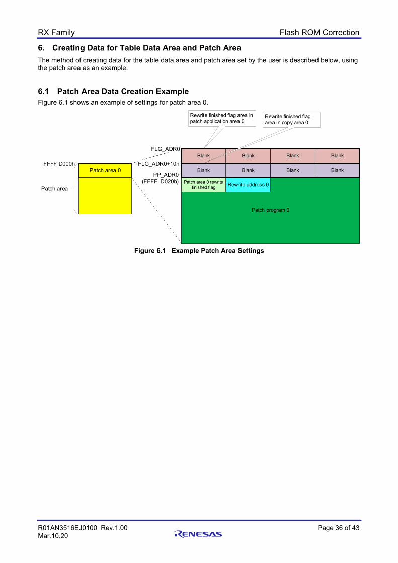
6. Creating Data for Table Data Area and Patch Area The method of creating data for the table data area and patch area set by the user is described below, using the patch area as an example.
6.1 Patch Area Data Creation Example Figure 6.1 shows an example of settings for patch area 0.
Figure 6.1 Example Patch Area Settings
FFFF D000hBlank
Patch program 0
FLG_ADR0
PP_ADR0(FFFF D020h)
Blank Blank Blank
Patch area 0 rewrite finished flag Rewrite address 0
Blank Blank Blank BlankFLG_ADR0+10h
Patch area 0
Patch area
Rewrite finished flag area in patch application area 0
Rewrite finished flag area in copy area 0
RX Family Flash ROM Correction
R01AN3516EJ0100 Rev.1.00 Page 37 of 43 Mar.10.20
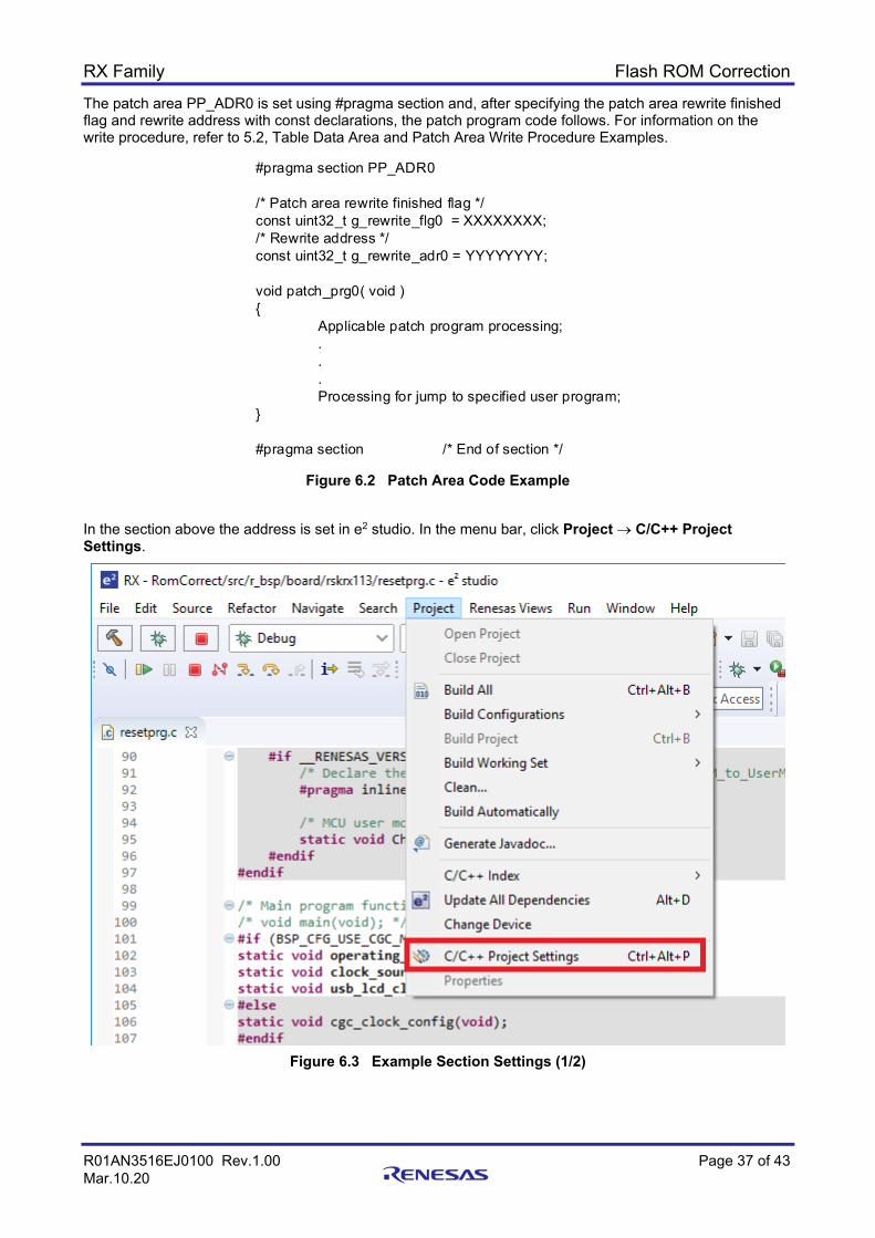
The patch area PP_ADR0 is set using #pragma section and, after specifying the patch area rewrite finished flag and rewrite address with const declarations, the patch program code follows. For information on the write procedure, refer to 5.2, Table Data Area and Patch Area Write Procedure Examples.
Figure 6.2 Patch Area Code Example
In the section above the address is set in e2 studio. In the menu bar, click Project → C/C++ Project Settings.
Figure 6.3 Example Section Settings (1/2)
#pragma section PP_ADR0
/* Patch area rewrite finished flag */const uint32_t g_rewrite_flg0 = XXXXXXXX;/* Rewrite address */const uint32_t g_rewrite_adr0 = YYYYYYYY;
void patch_prg0( void ){
Applicable patch program processing;...Processing for jump to specified user program;
}
#pragma section /* End of section */
RX Family Flash ROM Correction
R01AN3516EJ0100 Rev.1.00 Page 38 of 43 Mar.10.20
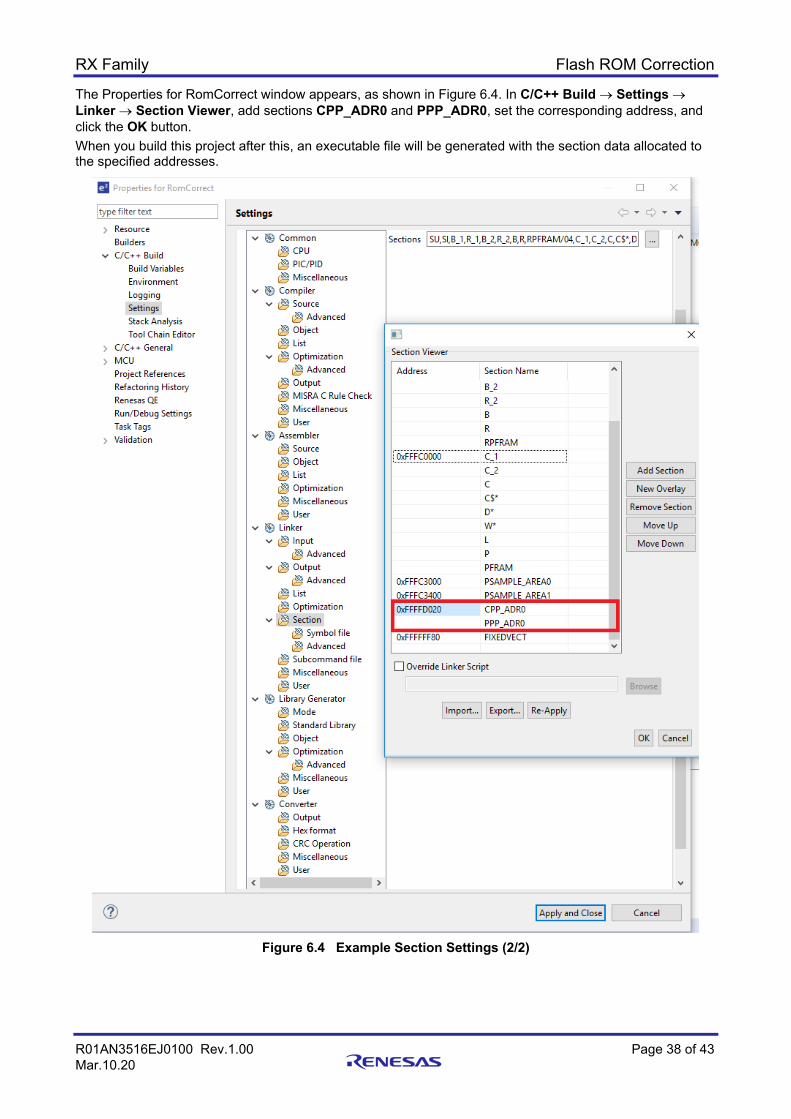
The Properties for RomCorrect window appears, as shown in Figure 6.4. In C/C++ Build → Settings → Linker → Section Viewer, add sections CPP_ADR0 and PPP_ADR0, set the corresponding address, and click the OK button. When you build this project after this, an executable file will be generated with the section data allocated to the specified addresses.
Figure 6.4 Example Section Settings (2/2)
RX Family Flash ROM Correction
R01AN3516EJ0100 Rev.1.00 Page 39 of 43 Mar.10.20
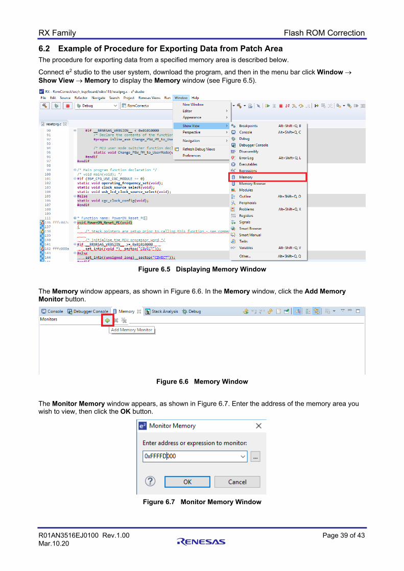
6.2 Example of Procedure for Exporting Data from Patch Area The procedure for exporting data from a specified memory area is described below.
Connect e2 studio to the user system, download the program, and then in the menu bar click Window → Show View → Memory to display the Memory window (see Figure 6.5).
Figure 6.5 Displaying Memory Window
The Memory window appears, as shown in Figure 6.6. In the Memory window, click the Add Memory Monitor button.
Figure 6.6 Memory Window
The Monitor Memory window appears, as shown in Figure 6.7. Enter the address of the memory area you wish to view, then click the OK button.
Figure 6.7 Monitor Memory Window
RX Family Flash ROM Correction
R01AN3516EJ0100 Rev.1.00 Page 40 of 43 Mar.10.20
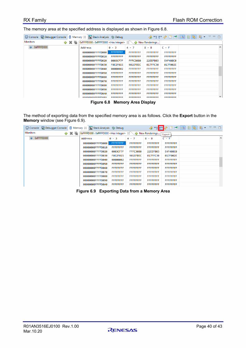
The memory area at the specified address is displayed as shown in Figure 6.8.
Figure 6.8 Memory Area Display
The method of exporting data from the specified memory area is as follows. Click the Export button in the Memory window (see Figure 6.9).
Figure 6.9 Exporting Data from a Memory Area
RX Family Flash ROM Correction
R01AN3516EJ0100 Rev.1.00 Page 41 of 43 Mar.10.20
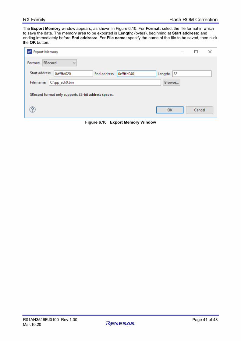
The Export Memory window appears, as shown in Figure 6.10. For Format: select the file format in which to save the data. The memory area to be exported is Length: (bytes), beginning at Start address: and ending immediately before End address:. For File name: specify the name of the file to be saved, then click the OK button.
Figure 6.10 Export Memory Window
RX Family Flash ROM Correction
R01AN3516EJ0100 Rev.1.00 Page 42 of 43 Mar.10.20
7. Sample Code Sample code can be downloaded from the Renesas Electronics website.
8. Reference Documents User’s Manual: Hardware
RX113 Group User’s Manual: Hardware (R01UH0448) (The latest version can be downloaded from the Renesas Electronics website.)
Technical Update/Technical News
(The latest information can be downloaded from the Renesas Electronics website.) User’s Manual: Development Tools
RX Family CC-RX Compiler User’s Manual (R20UT3248) (The latest version can be downloaded from the Renesas Electronics website.)
RX Family Flash ROM Correction
R01AN3516EJ0100 Rev.1.00 Page 43 of 43 Mar.10.20
Revision History
Rev. Date Description Page Summary
1.00 Mar. 10, 2020 First edition issued
General Precautions in the Handling of Microprocessing Unit and Microcontroller Unit Products The following usage notes are applicable to all Microprocessing unit and Microcontroller unit products from Renesas. For detailed usage notes on the products covered by this document, refer to the relevant sections of the document as well as any technical updates that have been issued for the products.
1. Precaution against Electrostatic Discharge (ESD)
A strong electrical field, when exposed to a CMOS device, can cause destruction of the gate oxide and ultimately degrade the device operation. Steps
must be taken to stop the generation of static electricity as much as possible, and quickly dissipate it when it occurs. Environmental control must be
adequate. When it is dry, a humidifier should be used. This is recommended to avoid using insulators that can easily build up static electricity.
Semiconductor devices must be stored and transported in an anti-static container, static shielding bag or conductive material. All test and
measurement tools including work benches and floors must be grounded. The operator must also be grounded using a wrist strap. Semiconductor
devices must not be touched with bare hands. Similar precautions must be taken for printed circuit boards with mounted semiconductor devices. 2. Processing at power-on
The state of the product is undefined at the time when power is supplied. The states of internal circuits in the LSI are indeterminate and the states of
register settings and pins are undefined at the time when power is supplied. In a finished product where the reset signal is applied to the external reset
pin, the states of pins are not guaranteed from the time when power is supplied until the reset process is completed. In a similar way, the states of pins
in a product that is reset by an on-chip power-on reset function are not guaranteed from the time when power is supplied until the power reaches the
level at which resetting is specified. 3. Input of signal during power-off state
Do not input signals or an I/O pull-up power supply while the device is powered off. The current injection that results from input of such a signal or I/O
pull-up power supply may cause malfunction and the abnormal current that passes in the device at this time may cause degradation of internal
elements. Follow the guideline for input signal during power-off state as described in your product documentation. 4. Handling of unused pins
Handle unused pins in accordance with the directions given under handling of unused pins in the manual. The input pins of CMOS products are
generally in the high-impedance state. In operation with an unused pin in the open-circuit state, extra electromagnetic noise is induced in the vicinity of
the LSI, an associated shoot-through current flows internally, and malfunctions occur due to the false recognition of the pin state as an input signal
become possible. 5. Clock signals
After applying a reset, only release the reset line after the operating clock signal becomes stable. When switching the clock signal during program
execution, wait until the target clock signal is stabilized. When the clock signal is generated with an external resonator or from an external oscillator
during a reset, ensure that the reset line is only released after full stabilization of the clock signal. Additionally, when switching to a clock signal
produced with an external resonator or by an external oscillator while program execution is in progress, wait until the target clock signal is stable. 6. Voltage application waveform at input pin
Waveform distortion due to input noise or a reflected wave may cause malfunction. If the input of the CMOS device stays in the area between VIL
(Max.) and VIH (Min.) due to noise, for example, the device may malfunction. Take care to prevent chattering noise from entering the device when the
input level is fixed, and also in the transition period when the input level passes through the area between VIL (Max.) and VIH (Min.). 7. Prohibition of access to reserved addresses
Access to reserved addresses is prohibited. The reserved addresses are provided for possible future expansion of functions. Do not access these
addresses as the correct operation of the LSI is not guaranteed. 8. Differences between products
Before changing from one product to another, for example to a product with a different part number, confirm that the change will not lead to problems.
The characteristics of a microprocessing unit or microcontroller unit products in the same group but having a different part number might differ in terms
of internal memory capacity, layout pattern, and other factors, which can affect the ranges of electrical characteristics, such as characteristic values,
operating margins, immunity to noise, and amount of radiated noise. When changing to a product with a different part number, implement a system-
evaluation test for the given product.
© 2020 Renesas Electronics Corporation. All rights reserved.
Notice 1. Descriptions of circuits, software and other related information in this document are provided only to illustrate the operation of semiconductor products
and application examples. You are fully responsible for the incorporation or any other use of the circuits, software, and information in the design of your product or system. Renesas Electronics disclaims any and all liability for any losses and damages incurred by you or third parties arising from the use of these circuits, software, or information.
2. Renesas Electronics hereby expressly disclaims any warranties against and liability for infringement or any other claims involving patents, copyrights, or other intellectual property rights of third parties, by or arising from the use of Renesas Electronics products or technical information described in this document, including but not limited to, the product data, drawings, charts, programs, algorithms, and application examples.
3. No license, express, implied or otherwise, is granted hereby under any patents, copyrights or other intellectual property rights of Renesas Electronics or others.
4. You shall not alter, modify, copy, or reverse engineer any Renesas Electronics product, whether in whole or in part. Renesas Electronics disclaims any and all liability for any losses or damages incurred by you or third parties arising from such alteration, modification, copying or reverse engineering.
5. Renesas Electronics products are classified according to the following two quality grades: “Standard” and “High Quality”. The intended applications for each Renesas Electronics product depends on the product’s quality grade, as indicated below. "Standard": Computers; office equipment; communications equipment; test and measurement equipment; audio and visual equipment; home
electronic appliances; machine tools; personal electronic equipment; industrial robots; etc. "High Quality": Transportation equipment (automobiles, trains, ships, etc.); traffic control (traffic lights); large-scale communication equipment; key
financial terminal systems; safety control equipment; etc. Unless expressly designated as a high reliability product or a product for harsh environments in a Renesas Electronics data sheet or other Renesas Electronics document, Renesas Electronics products are not intended or authorized for use in products or systems that may pose a direct threat to human life or bodily injury (artificial life support devices or systems; surgical implantations; etc.), or may cause serious property damage (space system; undersea repeaters; nuclear power control systems; aircraft control systems; key plant systems; military equipment; etc.). Renesas Electronics disclaims any and all liability for any damages or losses incurred by you or any third parties arising from the use of any Renesas Electronics product that is inconsistent with any Renesas Electronics data sheet, user’s manual or other Renesas Electronics document.
6. When using Renesas Electronics products, refer to the latest product information (data sheets, user’s manuals, application notes, “General Notes for Handling and Using Semiconductor Devices” in the reliability handbook, etc.), and ensure that usage conditions are within the ranges specified by Renesas Electronics with respect to maximum ratings, operating power supply voltage range, heat dissipation characteristics, installation, etc. Renesas Electronics disclaims any and all liability for any malfunctions, failure or accident arising out of the use of Renesas Electronics products outside of such specified ranges.
7. Although Renesas Electronics endeavors to improve the quality and reliability of Renesas Electronics products, semiconductor products have specific characteristics, such as the occurrence of failure at a certain rate and malfunctions under certain use conditions. Unless designated as a high reliability product or a product for harsh environments in a Renesas Electronics data sheet or other Renesas Electronics document, Renesas Electronics products are not subject to radiation resistance design. You are responsible for implementing safety measures to guard against the possibility of bodily injury, injury or damage caused by fire, and/or danger to the public in the event of a failure or malfunction of Renesas Electronics products, such as safety design for hardware and software, including but not limited to redundancy, fire control and malfunction prevention, appropriate treatment for aging degradation or any other appropriate measures. Because the evaluation of microcomputer software alone is very difficult and impractical, you are responsible for evaluating the safety of the final products or systems manufactured by you.
8. Please contact a Renesas Electronics sales office for details as to environmental matters such as the environmental compatibility of each Renesas Electronics product. You are responsible for carefully and sufficiently investigating applicable laws and regulations that regulate the inclusion or use of controlled substances, including without limitation, the EU RoHS Directive, and using Renesas Electronics products in compliance with all these applicable laws and regulations. Renesas Electronics disclaims any and all liability for damages or losses occurring as a result of your noncompliance with applicable laws and regulations.
9. Renesas Electronics products and technologies shall not be used for or incorporated into any products or systems whose manufacture, use, or sale is prohibited under any applicable domestic or foreign laws or regulations. You shall comply with any applicable export control laws and regulations promulgated and administered by the governments of any countries asserting jurisdiction over the parties or transactions.
10. It is the responsibility of the buyer or distributor of Renesas Electronics products, or any other party who distributes, disposes of, or otherwise sells or transfers the product to a third party, to notify such third party in advance of the contents and conditions set forth in this document.
11. This document shall not be reprinted, reproduced or duplicated in any form, in whole or in part, without prior written consent of Renesas Electronics. 12. Please contact a Renesas Electronics sales office if you have any questions regarding the information contained in this document or Renesas
Electronics products.
(Note1) “Renesas Electronics” as used in this document means Renesas Electronics Corporation and also includes its directly or indirectly controlled subsidiaries.
(Note2) “Renesas Electronics product(s)” means any product developed or manufactured by or for Renesas Electronics.
(Rev.4.0-1 November 2017)
Corporate Headquarters Contact information TOYOSU FORESIA, 3-2-24 Toyosu, Koto-ku, Tokyo 135-0061, Japan www.renesas.com
For further information on a product, technology, the most up-to-date version of a document, or your nearest sales office, please visit: www.renesas.com/contact/.
Trademarks Renesas and the Renesas logo are trademarks of Renesas Electronics Corporation. All trademarks and registered trademarks are the property of their respective owners.
Related Documents