IC-SP-06027 R0 Hitachi Single Chip Inverter IC Application Guide (Applicable models) VSP-input type 6-input type For @ AC115V ECN30102 ECN30105 ECN30107 ECN30611 For @ AC230V ECN30204 ECN30206 ECN30207 ECN30601 ECN30603 ECN30604 Development Department Power Device Division Hitachi, Ltd., Power Systems, Power & Industrial System Division

Welcome message from author
This document is posted to help you gain knowledge. Please leave a comment to let me know what you think about it! Share it to your friends and learn new things together.
Transcript

IC-SP-06027 R0
Hitachi Single Chip Inverter IC Application Guide
(Applicable models)
VSP-input type 6-input type
For @ AC115V ECN30102 ECN30105 ECN30107
ECN30611
For @ AC230V ECN30204 ECN30206 ECN30207
ECN30601 ECN30603 ECN30604
Development Department Power Device Division
Hitachi, Ltd., Power Systems, Power & Industrial System Division

IC-SP-06027 R0
Precautions for Safe Use and Notices If semiconductor devices are handled inappropriate manner, failures may result. For this reason, be sure to read this “Application Guide” before use.
This mark indicates an item about which caution is required.
This mark indicates a potentially hazardous situation which, if not avoided, may result in minor or moderate injury and damage to property.
CAUTION
(1) Regardless of changes in external conditions during use “absolute maximum ratings” should never be exceed in designing electronic circuits that employ semiconductors. In the case of pulse use, furthermore,²safe operating area(SOA)”precautions should be observed.
(2) Semiconductor devices may experience failures due to accident or unexpected surge voltages. Accordingly, adopt safe design features, such as redundancy or prevention of erroneous action, to avoid extensive damage in the event of a failure.
(3) In cases where extremely high reliability is required (such as use in nuclear power
control, aerospace and aviation, traffic equipment, life-support-related medical equipment, fuel control equipment and various kinds of safety equipment), safety should be ensured by using semiconductor devices that feature assured safety or by means of user’s fail-safe precautions or other arrangement. Or consult Hitachi’s sales department staff.
(If a semiconductor device fails, there may be cases in which the semiconductor device, wiring or wiring pattern will emit smoke or cause a fire or in which the semiconductor device will burst)
NOTICES 1. This Application Guide contains the specifications, characteristics(in figures and tables), dimensions
and handling notes concerning power semiconductor products (hereinafter called “products”) to aid in the selection of suitable products.
2. The specifications and dimensions, etc. stated in this Application Guide are subject to change without prior notice to improve products characteristics. Before ordering, purchasers are advised to contact Hitachi’s sales department for the latest version of this Application Guide and specifications.
3. In no event shall Hitachi be liable for any damage that may result from an accident or any other cause during operation of the user’s units according to this Application Guide. Hitachi assumes to responsibility for any intellectual property claims or any other problems that may result from applications of information, products or circuits described in this Application Guide.
4. In no event shall Hitachi be liable for any failure in a semiconductor device or any secondary damage resulting from use at a value exceeding the absolute maximum rating.
5. No license is granted by this Application Guide under any patents or other rights of any third party or Hitachi, Ltd.
6. This Application Guide may not be reproduced or duplicated, in any form, in whole or in part, without the expressed written permission of Hitachi, Ltd.
7. The products (technologies) described in this Application Guide are not to be provided to any party whose purpose in their application will hinder maintenance of international peace and safety nor are they to be applied to that purpose by their direct purchasers or any third party. When exporting these products (technologies), the necessary procedures are to be taken in accordance with related laws and regulations.
!
!
!
CAUTION

IC-SP-06027 R0
Hitachi offers even better products by taking advantage of our long years of experiences in the market.
Hitachi helps you save even more energy under our policy of "quality first."
Advanced Hitachi Single-chip Inverter ICs
Much easy to use It becomes easy to design the system power supply by the power supply up/down sequence free design of IC. *1).
Much reduce the effects on the environment
It conforms to lead (Pb) free phase category "Phase 3A" *4) of “electronic equipment” of JEITA *3) ETR-7021 (issue in June, 2004)".
Much strong noise-immunity
A built-in cancellation circuit designed to inhibit noises of no more than about 1 ms, reduces output malfunctions induced by noises in the input signal line *2).
*1) This applies to ECN30107s, ECN30611s, ECN30206s, ECN30207s, ECN30603s and ECN30604s. *2) This applies to ECN30204s, ECN30206s, ECN30207s, ECN30601s, ECN30603s and ECN30604s *3) JEITA: Japan Electronics and Information Technology Industries Association *4) Phase 3A: The entire parts must be lead-free, include the internal connection and the part materials,
that exclude exemption of EU RoHS *5) directive. *5) EU RoHS: DIRECTIVE 2002/95/EC OF THE EUROPEAN PARLIAMENT AND OF THE COUNCIL of
27 January 2003 on the restriction of the use of certain hazardous substances in electrical and electronic equipment

IC-SP-06027 R0
≪Contents≫
1. Overview
1-1. Dielectric isolation (DI) -------------------------------------------------------------------------------------------- 1 1-2. Single-chip Inverter ICs ------------------------------------------------------------------------------------------- 2 1-3. Composition of an inverter IC ---------------------------------------------------------------------------------- 2 1-4. Motor drive system ------------------------------------------------------------------------------------------------- 3 1-5. Block diagram of inverter ICs ----------------------------------------------------------------------------------- 3
2. Content of specification ------------------------------------------------------------------------------------------------ 4
3. Package
3-1. Model name ------------------------------------------------------------------------------------------------------------ 5 3-2. Production lot number --------------------------------------------------------------------------------------------- 5 3-3. Marking ------------------------------------------------------------------------------------------------------------------ 5 3-4. Package outline ------------------------------------------------------------------------------------------------------- 6
4. Pins
4-1. Pin arrangement ----------------------------------------------------------------------------------------------------- 8 4-2. Functions of the pins ---------------------------------------------------------------------------------------------- 9
5. Functions and operational precautions
5-1. Protection function ------------------------------------------------------------------------------------------------- 13 (1) Detection of VCC under voltage (2) Current limitation
(a) Operation description (b) How to set up (c) Noises of the RS pin (d) Precautions on wiring (e) Motor lock
(3) Protection against short circuit 5-2. Charge pump circuit ----------------------------------------------------------------------------------------------- 16
(1) Description of operation 5-3. Power supply sequence ------------------------------------------------------------------------------------------ 17 5-4. VB power supply ---------------------------------------------------------------------------------------------------- 18 5-5. Operation of the output IGBT of the VSP-input type --------------------------------------------------- 19
(1) PWM operation (2) Output all-off function
(a) Function description (b) Precautions
5-6. Internal Filter ---------------------------------------------------------------------------------------------------------- 20 5-7. Dead time -------------------------------------------------------------------------------------------------------------- 21 5-8. Calculation of power consumption ---------------------------------------------------------------------------- 24 5-9. Derating ---------------------------------------------------------------------------------------------------------------- 26
5-10. External components -------------------------------------------------------------------------------------------- 27

IC-SP-06027 R0
6. Handling Instruction 6-1 Mounting ---------------------------------------------------------------------------------------------------------------- 29
(1) Insulation between pins (2) Connection of tabs (3) Soldering conditions
6-2 Antistatic measures ------------------------------------------------------------------------------------------------ 30
7. Quality 7-1. Quality tests ----------------------------------------------------------------------------------------------------------- 30 7-2. QC Control Flow ----------------------------------------------------------------------------------------------------- 31
8. Inverter IC Handling Note
8-1. Electrical static destruction of VSP pin caused by external surge -------------------------------- 32 8-2. Electrical static destruction of FG pin caused by external surge --------------------------------- 32 8-3. IC destruction by external surge inputted to VS and VCC line (1) -------------------------------- 33 8-4. IC destruction by external surge inputted to VS and VCC line (2) -------------------------------- 33 8-5. IC destruction by external surge inputted to VS and VCC line (3) -------------------------------- 33 8-6. IC destruction by line noise put into VCC (1) ------------------------------------------------------------- 34 8-7. IC destruction by line noise put into VCC (2) ------------------------------------------------------------- 34 8-8. IC destruction by relay noise of inspection machine -------------------------------------------------- 35 8-9. Motor failure (missing phase output) ------------------------------------------------------------------------ 35
IC-SP-06027 R0
- 1 -
1. Overview
1-1. Dielectric isolation (DI)
Hitachi Intelligent Power IC A logical device and a power-switching device can be integrated in a
single chip. No mutual interference occurs, not only between devices but also
between device and board.
The Hitachi high-voltage monolithic IC is an intelligent power IC, developed based on a unique dielectric isolation
technology (DI). It is structured that there be no latch-up between devices and between device and board, and that
an IC can be made so a high-dielectric-strength, large-current output circuit is mixed with a logical circuit. The ICs
can be made smaller than conventional discrete boards and hybrid ICs. Latch-up-free IC offers wider range of applications.
The Hitachi high-voltage monolithic IC developed with dielectric isolation technology are such that the devices are
isolated with SiO2 layers in between, unlike P-N junction isolation. In consequence, it can remain latched-up free
even under high-temperature, large-current, high-noise, and other severe conditions. This technology also enables
them to be extremely flexible in circuit designing and thus to meet more customer requirement.
Die
lect
ric is
olat
ion
P-N
junc
tion
isol
atio
n
SiO2
Single crystal silicon
Poly silicon
SiO2
(Insulator separation layer)
Aluminum wire
SiO2
Single crystal silicon
P type silicon
Depletion layer (Insulator separation layer)
Aluminum wire
Fig. 1-1. Dielectric isolation and P-N junction isolation
P N
N N
P N
N N P+ P+
N

IC-SP-06027 R0
- 2 -
1-2. Single-chip Inverter ICs
Hitachi Single-chip Inverter ICs are monolithic ICs integrating various constituent devices and circuits required for
inverter control on a single chip with dielectric isolation technology. They are for driving motors, best suited for
controlling small three-phase brushless DC motors. The advantage of downsizing by the use of a single-chip structure
can be used to reduce the control board in size, which facilitates the incorporate of such ICs in motors.
1-3. Composition of an inverter IC
An inverter is a device that converts DC currents into AC. It can be used to drive motors for efficient variable-speed
control. Fig. 1-3 shows the basic configuration of an inverter IC required for that purpose. To drive the three-phase
motor with an inverter, six IGBTs and free wheel diodes are used as output stages. The IC consists of an IGBT driving
power circuit, level shift circuit, a logic circuit and other components for IGBT control. Hitachi Inverter ICs can directly
receive high voltage supplied from rectifying commercial AC power, because they have high dielectric strength. This
obviates the need of a step-down circuit, thus inhibiting efficiency cuts induced by voltage conversion.
Fig.1-3. Basic configuration of an inverter IC
Control Circuit
Logic Level Shift
(Single-chip inverter IC)
IGBT
(Can be incorporated in motors.)
IGBT Driver
Fig. 1-2. Single-chip inverter IC
15V
Rec
tifyi
ng/s
moo
thin
g ci
rcui
t
AC115V
Output Power device: IGBTs
High voltage 3-phase DCBLM Driver IC
m-Processor Position detection circuit
U V W
Motor
Charge pump circuit
Driver circuit Protection circuit Level shift circuit
Logic circuit
IC-SP-06027 R0
- 3 -
1-4. Motor drive system Three-phase inverters generally fall into two categories according to the method of commutation of the six output-stage
devices: 120-degree energization and 180-degree energization. The method of 120-degree energization is such that
the device on the top arm and that on the bottom arm are controlled to set the energization period between phases to
120 degrees, thus transferring the current from phase U to V to W, thus driving the motor. Hitachi Single-chip Inverter
ICs (VSP-input series) are based on 120-degree energization and receive position signals from hall ICs and VSP
signals that constitute speed instructions, thus conducting PWM control by the chopping action of the lower arm. For
uses of 180-degree energization, a six-input series are provided where six output stage devices can be controlled by
each input signal.
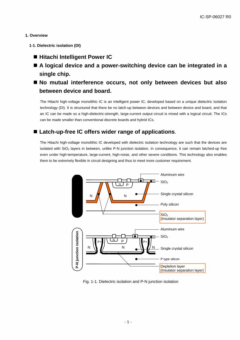
1-5. Block Diagram of Inverter IC Fig. 1-4 shows a block diagram of ECN30206 for receiving 230V AC, as an example of inverter IC. Its main function is
to receive input signals from the three phases of hall ICs of the brushless DC motor, turns on and off the particular
IGBTs with the three-phase distribution circuit, and to drive the motor. Other components include a charge pump circuit
as a power self-supply circuit, a triangular wave oscillator and a comparator-based PWM generation circuit as rpm
control circuits, an over current detection circuit which provides a current trip function at motor startup, and an under
voltage detection circuit that detects power drops in the drive circuit and turns off the output.
Fig.1-4. Block diagram of ECN30206
Filte
r Circ
uit
CMP - +
CMP +
-
- +
PWM Comparator
VCC
VCC
Clock
GH1
Charge Pump
VS1 VS2
MU
MV
MW
CL
GL
VS
Clock
SAW wave Generator
VTR
D2 D1
C1 C2 +
+ - -
RTR
CTR
Over Current Sense
HU HW HV
CR
Vref
RS
RS
RU
RV
RW
Hall ICs
VSP
VCC VB
CB
C0 VCC(15V)
C+ C-
GH2
FG FG
DM
Note : Inside of bold line shows ECN30206
Bottom arm off
All off
Motor Bottom Arm
Driver
Top Arm Driver Motor Rotating
Direction Micro Controller
or Analog Output
LVSD
VB supply
3-Phase Distributor

IC-SP-06027 R0
- 4 -
2. Content of specifications
The following items have been described in the specifications.
(1) Maximum Ratings · It describes direct conditions(electric, thermal use conditions) of leading to IC destruction and so on. And
the safety operating range with operating conditions is shown by minimum or maximum value. · Each item is an independent item. Also, these items show the ratings value of not exceeding any use
conditions. The maximum rating and other characteristics are mutually related, and not permitted at the same time.
(2) Electrical Characteristics
· It provides for an electric characteristic item that shows the function of IC, and describes minimum, standard, and maximum.
(3) Function and Operation
· It describes Truth Table, Time Chart, Protection Function and so on.
(4) Standard application · It describes external parts to operate IC.
(5) Pin Assignments and Pin Definitions · It describes pin assignments, pin names and pin definitions.
(6) Important notice Precautions · It describes notes of the static electricity, the maximum rating, handling and so on.
(7) Appendix and Reference data · It describes SOA and Deratings.

IC-SP-06027 R0
- 5 -
3. Package
3-1. Model name
ECN 30206 SP Package type (SP, SPV, SPR) Series name Hitachi High-voltage IC
3-2. Production lot number
5 E 12 F Control number
It shows by two digits or less (alphabetical character). Lead (Pb) Free: Last digit is Marked as “F”
Quality control number.
It shows by one digit or two digits. (Numerals from 1 to 9, alphabetical character (except O and I) or space is used.)
Assembled month as shown in below
January, A; February, B; March, C; April, D; May, E; June, K; July, L; August, M; September, N; October, X; November, Y; and December, Z
Least significant digit of Assembled year (A.D.)
3-3. Marking
Fig. 3-1. Marking diagram
J A P N A
Model name
Production lot Index pin Hitachi

IC-SP-06027 R0
- 6 -
3-4. Package Outline
Table 3-1(1). Package Dimensions (unit: mm) Package Type Package Dimensions
SP
(SP-23TA)
SPV
(SP-23TB)
1
1

IC-SP-06027 R0
- 7 -
Table 3-1(2). Package Dimensions (unit: mm)
Package Type Package Dimensions
SPR
(SP-23TR)
1 23

IC-SP-06027 R0
- 8 -
4. Pins 4-1. Pin assignments
Table 4-1. Assignment table of pins Applicable
Model Pin #
ECN30102 ECN30105 ECN30107 ECN30207
ECN30204 ECN30206
ECN30611 ECN30601 ECN30603 ECN30604
1 VS2 VS2 VS2 2 MW MW MW 3 NC note1 NC note1 NC note1 4 GH2 GH2 GH2 5 VCC VCC VCC 6 GL GL GL 7 C+ C+ C+ 8 C- C- C- 9 CL CL CL 10 CB CB CB 11 CTR CTR CTR 12 VTR VTR VTR 13 VSP VSP WB 14 FG FG VB 15 NC note1 DM UB 16 HW HW RS 17 HV HV WT 18 HU HU VT 19 RS RS UT 20 GH1 GH1 GH1 21 MU MU MU 22 VS1 VS1 VS1 23 MV MV MV
Note 1: NC represents an unconnected pin. It is not connected to an internal chip.

IC-SP-06027 R0
- 9 -
4-2. Functions of the pins Table 4-2. List of pins and their functions (pins common to all models) No. Pin Item Functions and Precautions Related items Remarks 1 VCC Control power supply pin · Powers the drive circuits for the top
and bottom arms, the charge pump circuit, the built-in VB supply circuit, and others.
· Determine the capacity of the power supply for VCC allowing a margin by adding the standby current Icc and the current taken out of CB pin.
· 5-1. (1) VCC under voltage Detection · 5-3. Power supply
sequence · 8-3 to 8-7
IC destruction by external surge or line noise
2 VS1 VS2
IGBT power pin · Connected to the collector of the top arm IGBT.
· Connect pins VS1 and VS2 close to the IC pin. If either pin is open, the IC may get destroyed.
· 5-3. Power supply sequence
· 8-3 to 8-5 IC destruction by external surge
High voltage pin
3 CB Output pin of the build-in VB supply
· Outputs a voltage (typ 7.5V) generated in the build-in VB power supply.
· Provides power from the VB power supply to the input, three-phase distribution, FG, internal clock, over current detection, and other circuits.
· Connect a capacitor C0 to prevent oscillation to the CB pin. Capacitor with capacity of 0.22mF ±20% is recommended
· 5-4. VB power supply
Top arm drive circuit power pin Charge pump circuit pin
· Powers the drive circuit for the top arm.
· Connect external components (capacitor and diode).
· 5-2. Charge pump circuit 4 C+ C- CL
High voltage pin
5 GL Control ground pin · It is the ground pin for VCC and VB power lines.
6 GH1 GH2
IGBT Emitter pin · Connected to the emitter of the bottom arm IGBT.
· Connected to a shunt resistor Rs to detect over currents.
· Connect the GH1 and GH2 near the IC pin. If either pin is open, the IC may get destroyed.
· 5-1. (2) Current limitation
CL
C+
C- VS1 VS2
MU MV MW
GH1 GH2
GL
Top armdriver
Internal clock
Equivalent Circuit
IC-SP-06027 R0
- 10 -
Table 4-2. List of pins and their functions (pins common to all models) <Continued> No. Pin Item Functions and Precautions Related items Remarks
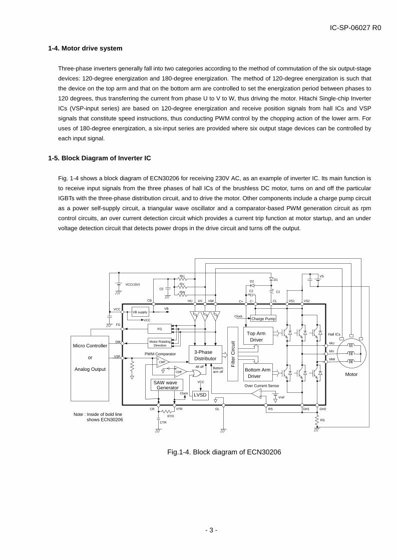
PWM frequency setting pin (VSP-input type) Clock frequency setting pin (6-input type)
· Externally connected resistors and capacitors are used to determine the frequency of the PWM (internal clock).
· Frequencies are roughly determined by the following equation:
f @ 0.494/(C X R) (Hz)
· 5-5. (1) PWM operation 7 CR VTR
8 MU MV MW
Inverter output pin · It is an output of a three-phase bridge consisting of six IGBTs and free wheel diodes.
High-voltage pin
Input pin for over current detection signals
· Monitors the voltage of the Rs shunt resistor and detects its over current status.
· 5-1. (2) Current limitation 9 RS
VTR
CR - +
VB
VSAWH(typ. 5.4V)
VSAWL(typ. 2.1V) H
L
VB
typ.50W
CompaInput resistor (note 1)
Switch selection by comparator output
Vref
typ. 220kW typ. 200kW
VB
RS typ. 5pF
S
R + -
Latch
Interlock clock trigger
Input resistor (note 1)
Equivalent Circuit
(Internal clock)
Input resistor value
· typ.300W ECN30102 ECN30107 ECN30206 ECN30207 ECN30611 ECN30603 ECN30604
· typ.150W
ECN30105 ECN30204 ECN30601
Equivalent Circuit
Input resistor value
· typ.300W ECN30102 ECN30107 ECN30206 ECN30207 ECN30611 ECN30603 ECN30604
· typ.150W
ECN30105 ECN30204 ECN30601
note 1)
note 1)

IC-SP-06027 R0
- 11 -
Table 4-3. List of pins and their functions (pin different according to model)
No. Pin Item Applicable
models Functions and Precautions Related items
Speed instruction input pin
ECN30102 ECN30105 ECN30107 ECN30204 ECN30206 ECN30207
· Input a speed instruction signal to generate a PWM signal.
· Entering an all-off operating voltage of the VSP terminal (typ. 1.23V) turns off all IGBTs.
· If a noise is detected, install a resistor and/or capacitor.
· 5-3. Power supply sequence · 5-5. Operation of the output IGBT of the VSP input type · 8-1. Electrical static destruction of
VSP pin caused by external surge
Data Sheet · 4.2 Input terminals
VSP
Hall signal input pin
ECN30102 ECN30105 ECN30107 ECN30204 ECN30206 ECN30207
· Input a hall IC signal. Based on that signal, the system controls the phase switchover of the output IGBT.
· If a noise is detected, install a capacitor. · The maximum input voltage is VB+0.5V.
The output voltage of hall IC must not exceed the maximum input voltage.
Data Sheet · 3.1. Truth table · 4.2. Input Pins
2 HU HV HW
ECN30102 ECN30105 ECN30107
· Output pulses according to the input signals of the HU, HV and HW.
· Motor rotation speed can be monitored by measuring the frequency of output pulse.
Motor rotation speed monitoring pin ECN30204
ECN30206 ECN30207
· Output pulses according to the input signals of the HU, HV and HW.
· Motor rotation speed can be monitored by measuring the frequency of output pulse.
· Connect an external circuit such as a pull-up resistor of around 5kW to 10kW to VCC or CB pin.
· 8-2. Electrical static destruction of FG pin caused by external surge
Data Sheet · 3.2 Time chart
3 FG
Input resistor value
· typ. 300W ECN30102 ECN30107 ECN30206 ECN30207
· typ. 150W
ECN30105 ECN30204 Equivalent Circuit
VSP
typ. 200kW
VB
+ -
Input resistor (note 1)
From CR pin
Comparator
Equivalent Circuit
Input resistor value
· typ. 300W ECN30102 ECN30107 ECN30206 ECN30207
· typ. 150W
ECN30105 ECN30204
VB
HU HV HW
typ. 200kW
Input resistor (note 1)
VB
FG
VCC
FG
Equivalent Circuit Equivalent Circuit
CMOS output type
Applicable models ECN30102 ECN30105 ECN30107
Open drain output type
Applicable models ECN30204 ECN30206 ECN30207
note 1)
note 1)

IC-SP-06027 R0
- 12 -
Table 4-3. List of pins and their functions (pins common to all models) <Continued> No. Pin Item
Applicable models Functions and Precautions Related items
ECN30204 ECN30206
· High or Low level output according to the input signal of the HU, HV and HW.
· Direction of motor rotation can be detected by measuring output voltage.
· Connect an external circuit such as a pull-up resistor of around 5kW to 10kW to VCC or CB pin.
· Direction of motor rotation relates to the DM output, as shown below ;
4 DM Direction of motor rotation detecting pin
ECN30611 ECN30601 ECN30603 ECN30604
· Input control signals of each arm. · In each input, input the High level turns on
the output IGBT. The UT, VT, and WT correspond to the top arm output IGBT.
· The UB, VB, and WB corrrespond to the bottom arm output IGBT.
· The input voltage is 5V CMOS or TTL logic level compatible.
· If a noise is detected, install a resistor and/or capacitor.
· The maximum input voltage is VB+0.5V.
· 5-3. Power supply sequence · 5-7. Dead time Data sheet · 4.2. Input Pins
5 UT VT WT UB VB WB
Control input pin of each arm
U --> V --> W LU --> W --> V H
DM outputDirection ofmotor rotation
VCC
DM
Equivalent Circuit
VB UT VT WT
UB VB WB
typ. 200kW
Input resistor (note 1)
Equivalent Circuit
Input resistor value
· typ. 300W ECN30611 ECN30603 ECN30604
· typ. 150W
ECN30601
note 1)

IC-SP-06027 R0
- 13 -
5. Functions and operational precautions
5-1. Protection function (1) Detection of VCC under voltage (LVSD operation)
· When the VCC voltage goes below the LVSD operating voltage (LVSDON), the output IGBTs of the top and bottom arms are all turned off regardless of the input signal.
· This function has hysteresis (Vrh). When the VCC voltage goes up again, the system goes back to a state where the ouput IGBT operates according to the input signal at a level equal to or exceeding the LVSD recovery voltage (LVSDOFF).
Fig. 5-1. Timing chart for detection of VCC under voltage (LVSD operation)
(2) Current limitation (a) Operation description
· The system monitors the current flowing through the shunt resistance Rs at the RS pin (see Fig. 5-2). When the reference voltage for current limitation (Vref = typ. 0.5V) is exceeded, the IGBT of the bottom arm is turned off.
· Reset after current limitation is performed in each cycle of the internal clock signal (VTR pin voltage). (See Fig.5-3.)
Fig. 5-2. Current of shunt resistance (typical)
LVSD operation voltage (LVSDON)
All off regardless of the input signal
LVSD recovery voltage (LVSDOFF)
VCC voltage LVSD operation
LVSD hysteresis (Vrh)
LVSD recovery
Operation according to the input signal
IGBT
operation (LVSD operation status)
Operation according to the input signal
VS
GH1
VS1 VS2
MU MV MW
RS
GH2RS
Is
+-
Vref
Motor

IC-SP-06027 R0
- 14 -
Fig. 5-3. Timing chart for current limitation
(b) How to set up · The current limitation setting IO is calculated as follows ;
IO = Vref / Rs where Vref: Standard voltage for current limitation Rs: Shunt resistor
· In setting a current limit, you should allow for Vref variance, Rs resistance variance, and the delay between the time the over current limitation is detected and the time the IGBT is turned off.
· This function is not effective for currents that do not flow forward through the shunt resistor, such as reflux current and power regenerative current (see Figs. 5-4 and 5-5). In practice, users are requested to observe and check the output currents (the coil currents of the motor) of the IC.
Power Supply current IS
VTR pin voltage
Reset signal
Current limit setting IO
Delay
OFF Lower arm IGBT operation ON ON
IGBT off
Over current detected
Current limitation reset
Current limitation performed
Delay

IC-SP-06027 R0
- 15 -
(c) Noises of the RS pin · The RS pin contains a filter having a time constant of about 1ms. · If the system malfunctions due to a noise, an effective solution is to add a filter externally. However,
beware that the external filter increases the delay time before the IGBT turns off.
(d) Precautions on wiring · Make the wiring of the shunt resistor Rs as short as possible. The GH1 and GH2 are connected to the
IGBT emitter. If the wiring has a high resistance or inductance component, the emitter potential of the IGBT changes, perhaps resulting in the IGBT malfunctioning.
· Connect the GH1 and GH2 pins near the pin. If the resistance components of the wiring is poor balanced between the GH1 and GH2 pins and the shunt resistor Rs, the current limit levels in each phase may not be equal.
(e) Motor lock
· This IC does not contain a protection function against motor lock. · If the motor locks, the phase where the output IGBT turns on is fixed, resulting in a constant
current-limited state. This produces a major loss, which results in IC temperature increase and IC gets destroyed.
(3) Protection against short-circuit · This IC does not contain a protection function against short-circuits (such as load short-circuit, earth fault,
and short-circuit between the top and bottom arms). · A short-circuit produces a large current exceeding the maximum rating in the IC. The IC may therefore
get destroyed.
VS
GH1
VS1 VS2
MUMVMW
RS
Motor
GH2RS
Fig. 5-4. Example to Reflux current
VS
GH1
VS1 VS2
MUMVMW
RS
Motor
GH2RS
Fig. 5-5. Example to Power regenerative current
Interlock clock trigger (Inside the IC)
Vref
typ. 220kW typ. 200kW
Input resistor (Note)
VB
typ. 5pF Latch S
R
Comparator
+- Rf
Cf Rs
GH1, GH2
External filter
RS
Note) See the section "RS" of Pin Name in Table 4.2 for the input resistor value.
Fig. 5-6. Example to add external filter

IC-SP-06027 R0
- 16 -
5-2. Charge pump circuit
(1) Description of operation · Fig. 5-7 shows a block diagram of a charge pump circuit. The SW1 and SW2 repeat turning on and off
alternatively, synchronously with the internal clock. · When the SW1 is off and the SW2 is on, the CL pin has a potential of 0V. Through the passage (1),
charge the capacitor C1. · Next, the SW1 is turned on and the SW2 is turned off, and the CL pin rises in potential to the VS level.
Through the passage (2), the charge of the capacitor C1 is pumped up to the capacitor C2. · This operation is repeated with the frequency of the internal clock, and the charge is given to the
capacitor C2. · The capacitor C2 constitutes a power supply for the drive circuit for the top arm.
Fig. 5-7. Charge pump circuit
Vcc Internal clock
Top arm Driver
+ -
+ -
C1
C2
SW1
SW2
D1
D2
CL
C+ C-
VS1,VS2
MU, MV, MW
GH1,GH2
Vs
GL
(1)
(2)

IC-SP-06027 R0
- 17 -
5-3. Power supply sequence (1) Power supply sequence free type
· ECN30107, ECN30611, ECN30207, ECN30604, ECN30206 (below 1A), ECN30603 (below 1A)
(2) Power supply sequence setting type of the VSP-input type and 6-input type is described below. · ECN30102, ECN30105, ECN30204 : Refer to (3) (a) VSP-input type · ECN30601 : Refer to (3) (b) 6-input type
(3) How to set Power supply sequence (a) VSP-input type
· Recommended sequences are as follows: At power-up: VCC on --> VS on --> VSP on At power-down: VSP off --> VS off --> VCC off If any sequence is involved other than those specified above, please refer to Tables 5-1 and 5-2.
· When the VSP is no higher than the VSAWL, the power sequence is free. · As for the sequences No. 2 and 5 in Table 5-1, if the VS line gets noisy before the VS is powered up after
the VCC and VSP are applied, the ON signal of the upper arm IGBT is reset and the motor may not start up. In such a case, first reduce the VSP to a level no higher than the all-off operating voltage (Voff), then apply it.
· In the case of No. 4 and 6 in Table 5-1 and No. 4 and 6 in Table 5-2, see "Current Derating for Power Sequence and Vcc Voltage" of the Product Specifications.
Table 5-1 Power up sequence (VSP-input type) Table 5-2 Power down sequence (VSP-input type)
No. (1) (2) (3) Permit or
Inhibit No. (1) (2) (3) Permit or
Inhibit 1 VCC VS VSP Permit 1 VSP VS VCC Permit 2 VCC VSP VS Permit 2 VS VSP VCC Permit 3 VS VCC VSP Permit 3 VSP VCC VS Permit 4 VS VSP VCC Inhibit 4 VCC VSP VS Inhibit 5 VSP VCC VS Permit 5 VS VCC VSP Permit 6 VSP VS VCC Inhibit 6 VCC VS VSP Inhibit
(b) 6-input type
· Recommended sequences are as follows ; At power-up: VCC on --> VS on --> "Control input" on At power-down: "Control input" off --> VS off --> VCC off For any sequence other than those specified above, see Tables 5-3 and 5-4.
· The power sequence is free if the lower arm control inputs UB, VB, and WB are all low (L) and if the upper control inputs UT, VT, and WT are all low (L).
· In the sequences No. 2 and 5 in Table 5-3, after the VCC and "control input" are applied, when a noise enters the VS line before VS power-up, the ON signal of the top arm IGBT can be reset and the motor may not start up. In such a case, the control inputs (UT, VT, and WT) for the top arm should be set to low, then power the system up again.
· In the case of No. 4 and 6 in Table 5-3 and No. 4 and 6 in Table 5-4, see "Current Derating for power supply sequence and Vcc voltage" of the product specifications.
Table 5-3 Power up sequence (6-input type) Table 5-4 Power down sequence (6-input type)
No. (1) (2) (3) Permit or
Inhibit No. (1) (2) (3) Permit or
Inhibit 1 VCC VS Control Input Permit 1 Control Input VS VCC Permit 2 VCC Control Input VS Permit 2 VS Control Input VCC Permit 3 VS VCC Control Input Permit 3 Control Input VCC VS Permit 4 VS Control Input VCC Inhibit 4 VCC Control Input VS Inhibit 5 Control Input VCC VS Permit 5 VS VCC Control Input Permit 6 Control Input VS VCC Inhibit 6 VCC VS Control Input Inhibit

IC-SP-06027 R0
- 18 -
5-4. VB power supply
· The VB power (VB = typ. 7.5V) to be output to the CB pin is generated at the VCC power. The VB power is supplied to the IC internal circuits such as the triangular wave oscillation circuit, over current detection circuit and so on.
· The VB power circuit constitutes a feedback circuit (see Fig. 5-8). To prevent oscillation, connect a capacitor C0 to the CB pin.
· The recommended capacity for the C0 is 0.22mF ± 20%. If any value other than the recommended one is to be used, refer to the below precautions and determine a suitable capacity.
<Precautions>
· As shown in Fig. 5-9, the CB pin may be oscillated depending on the C0 capacity and the output current IB.
· The larger the C0 capacity is, the more stable the VB power supply is. It is recommended, however not to set the capacity figure to an excessive level. As a guide, it should be 2m to 3mF or less in the non-oscillated region.
Fig. 5-8. Equivalent circuit for the VB power supply
Fig.5-9. IB and C0 dependence of CB pin oscillation (reference data)
VCC pin
CB pin
C0
IB
Reference Voltage source
Internal circuit
External circuit
(Inside the IC)
0.01
0.1
1
10
0 5 10 15 20 25 30
Output current IB for VB power supply (mA)
C0
( mF
)
Oscillation
Specification: 25mA maximum

IC-SP-06027 R0
- 19 -
5-5. Operation of the output IGBTs of the VSP-input type (Applicable models: ECN30102, ECN30105, ECN30107, ECN30204, ECN30206, ECN30207)
(1) PWM operation
· PWM signals are generated by comparing the VSP input voltage and triangular signal (CR pin voltage). · Chopping with PWM is conducted by the lower arm. (See Fig.5-10.)
VSP input voltage > triangular signal; the lower arm IGBT on VSP input voltage < triangular signal; lower arm IGBT off
· The PWM duty varies linearly between the bottom limit (VSAWL = typ. 2.1V) and the top limit (VSAWH = typ. 5.4V) of the triangular wave amplitude level. It becomes 0% at VSAWL, and 100% at VSAWH.
Fig. 5-10. Timing chart of PWM operation
(2) Output all-off function
(a) Function description · When the input voltage of the VSP pin reaches or goes below the all-off operation voltage (Voff = typ
1.23V), this function turns off all the output IGBTs. The operation of the output IGBTs with regard to the VSP input voltage conforms to Table 5-5.
Table 5-5. Operation of the output IGBTs with regard to VSP input voltage
VSP input voltage Top arm IGBT Bottom arm IGBT
0V≦VSP<Voff ( typ. 1.23V) All off All off
Voff (typ. 1.23V) ≦VSP<VSAWL (typ. 2.1V) As per hall signal input All off
VSAWL (typ. 2.1V) ≦VSP As per hall signal input As per hall signal input
(b) Precautions · When the output all-off function is activated while the motor is rotating, a regenerative current is
generated in the VS power supply, in some cases resulting in the VS power voltage rise. Keep the VS pin voltage equal to or below the maximum rating. Attention is particularly needed, when the capacity between the VS and GND is small, where the voltage is more likely to rise.
Triangular wave signal (CR pin voltage)
VSP input voltage
VSAWL (typ. 2.1V)
VSAWH (typ. 5.4V)
Power supply current IS
Motor coil current
Lower arm IGBT ON ON ON ON OFF OFF OFF OFF
IC-SP-06027 R0
- 20 -
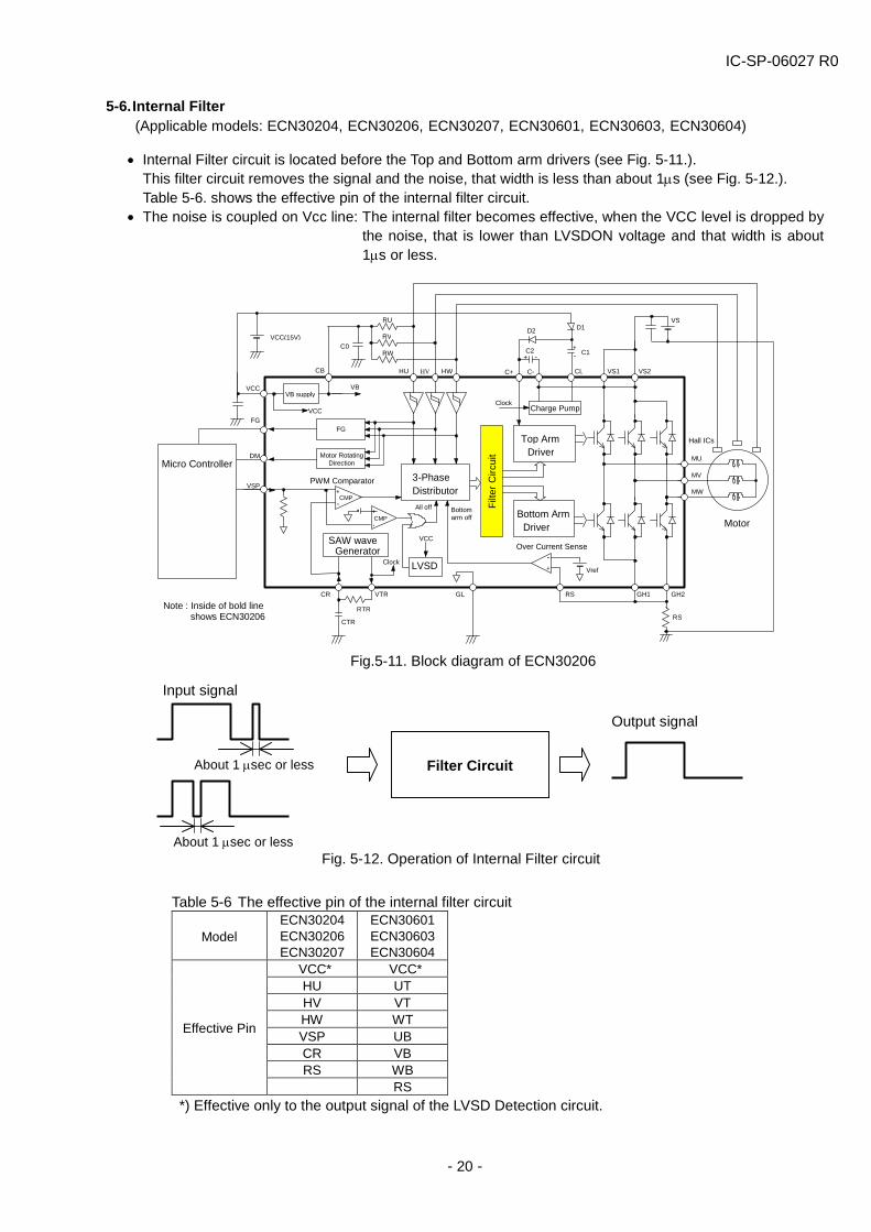
5-6. Internal Filter (Applicable models: ECN30204, ECN30206, ECN30207, ECN30601, ECN30603, ECN30604)
· Internal Filter circuit is located before the Top and Bottom arm drivers (see Fig. 5-11.). This filter circuit removes the signal and the noise, that width is less than about 1ms (see Fig. 5-12.). Table 5-6. shows the effective pin of the internal filter circuit.
· The noise is coupled on Vcc line: The internal filter becomes effective, when the VCC level is dropped by the noise, that is lower than LVSDON voltage and that width is about 1ms or less.
Table 5-6 The effective pin of the internal filter circuit
Model ECN30204 ECN30206 ECN30207
ECN30601 ECN30603 ECN30604
VCC* VCC* HU UT HV VT HW WT VSP UB CR VB RS WB
Effective Pin
RS *) Effective only to the output signal of the LVSD Detection circuit.
Filter Circuit About 1 msec or less
About 1 msec or less
Input signal
Output signal
Fig. 5-12. Operation of Internal Filter circuit
Fig.5-11. Block diagram of ECN30206
Filte
r Circ
uit
CMP - +
CMP +
-
- +
PWM Comparator
VCC
VCC
Clock
GH1
Charge Pump
VS1 VS2
MU
MV
MW
CL
GL
VS
Clock
SAW wave Generator
VTR
D2 D1
C1 C2 +
+ - -
RTR
CTR
Over Current Sense
HU HW HV
CR
Vref
RS
RS
RU
RV
RW
Hall ICs
VSP
VCC VB
CB
C0 VCC(15V)
C+ C-
GH2
FG FG
DM
Note : Inside of bold line shows ECN30206
Bottom arm off
All off
Motor Bottom Arm
Driver
Top Arm Driver Motor Rotating
Direction Micro Controller
LVSD
VB supply
3-Phase Distributor
IC-SP-06027 R0
- 21 -
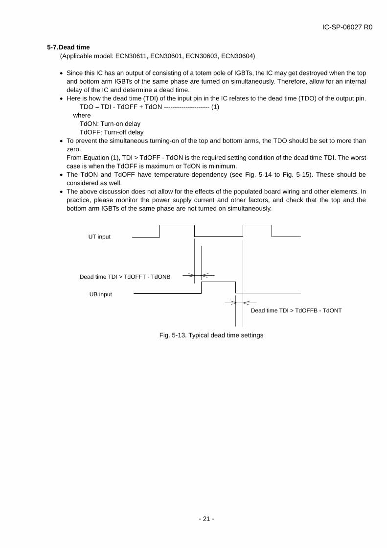
5-7. Dead time (Applicable model: ECN30611, ECN30601, ECN30603, ECN30604)
· Since this IC has an output of consisting of a totem pole of IGBTs, the IC may get destroyed when the top
and bottom arm IGBTs of the same phase are turned on simultaneously. Therefore, allow for an internal delay of the IC and determine a dead time.
· Here is how the dead time (TDI) of the input pin in the IC relates to the dead time (TDO) of the output pin. TDO = TDI - TdOFF + TdON --------------------- (1)
where TdON: Turn-on delay TdOFF: Turn-off delay
· To prevent the simultaneous turning-on of the top and bottom arms, the TDO should be set to more than zero. From Equation (1), TDI > TdOFF - TdON is the required setting condition of the dead time TDI. The worst case is when the TdOFF is maximum or TdON is minimum.
· The TdON and TdOFF have temperature-dependency (see Fig. 5-14 to Fig. 5-15). These should be considered as well.
· The above discussion does not allow for the effects of the populated board wiring and other elements. In practice, please monitor the power supply current and other factors, and check that the top and the bottom arm IGBTs of the same phase are not turned on simultaneously.
Fig. 5-13. Typical dead time settings
UT input
UB input
Dead time TDI > TdOFFT - TdONB
Dead time TDI > TdOFFB - TdONT

IC-SP-06027 R0
- 22 -
ECN306011 ECN30601
Turn
on
dela
y tim
e
(Top
arm
)
Turn
on
dela
y tim
e
(Bot
tom
arm
)
Turn
off
dela
y tim
e
(Top
arm
)
Turn
off
dela
y tim
e
(Bot
tom
arm
)
Fig. 5-14 Temperature-dependency of TdON and TdOFF (1)
0.0
1.0
2.0
3.0
4.0
-30 0 30 60 90 120 150 Temperature Tj (oC)
TdO
NT(
ms)
0.0
1.0
2.0
3.0
4.0
-30 0 30 60 90 120 150 Temperature Tj (oC)
TdO
NT(
ms)
0.0
1.0
2.0
3.0
4.0
-30 0 30 60 90 120 150 Temperature Tj (oC)
TdO
NB
(ms)
0.0
1.0
2.0
3.0
4.0
-30 0 30 60 90 120 150 Temperature Tj (oC)
TdO
FFT(
ms)
0.0
1.0
2.0
3.0
4.0
-30 0 30 60 90 120 150 Temperature Tj (oC)
TdO
FFB
(ms)
0.0
1.0
2.0
3.0
4.0
-30 0 30 60 90 120 150 Temperature Tj (oC)
TdO
NB
(ms)
0.0
1.0
2.0
3.0
4.0
-30 0 30 60 90 120 150 Temperature Tj (oC)
TdO
FFT(
ms)
0.0
1.0
2.0
3.0
4.0
-30 0 30 60 90 120 150 Temperature Tj (oC)
TdO
FFB
(ms)

IC-SP-06027 R0
- 23 -
ECN30603 ECN30604
Turn
on
dela
y tim
e
(Top
arm
)
Turn
on
dela
y tim
e
(Bot
tom
arm
)
Turn
off
dela
y tim
e
(Top
arm
)
Turn
off
dela
y tim
e
(Bot
tom
arm
)
Fig. 5-15 Temperature-dependency of TdON and TdOFF (2)
0.0
1.0
2.0
3.0
4.0
-30 0 30 60 90 120 150 Temperature Tj (oC)
TdO
NT(
ms)
0.0
1.0
2.0
3.0
4.0
-30 0 30 60 90 120 150 Temperature Tj (oC)
TdO
NT(
ms)
0.0
1.0
2.0
3.0
4.0
-30 0 30 60 90 120 150 Temperature Tj (oC)
TdO
NB
(ms)
0.0
1.0
2.0
3.0
4.0
-30 0 30 60 90 120 150 Temperature Tj (oC)
TdO
FFT(
ms)
0.0
1.0
2.0
3.0
4.0
-30 0 30 60 90 120 150 Temperature Tj (oC)
TdO
FFB
(ms)
0.0
1.0
2.0
3.0
4.0
-30 0 30 60 90 120 150 Temperature Tj (oC)
TdO
NB
(ms)
0.0
1.0
2.0
3.0
4.0
-30 0 30 60 90 120 150 Temperature Tj (oC)
TdO
FFT(
ms)
0.0
1.0
2.0
3.0
4.0
-30 0 30 60 90 120 150 Temperature Tj (oC)
TdO
FFB
(ms)
IC-SP-06027 R0
- 24 -
5-8. Calculation of power consumption · Here are simple formulae for calculating of power consumption generated in the VSP-input type and the
six-input type. As for the constant required for calculation, contact our sales representative.
(1) VSP-input type (Inverter controlled 120-degree commutation mode, bottom arm PWM chopping) (Applicable models: ECN30102, ECN30105, ECN30107, ECN30204, ECN30206, ECN30207)
Total IC power consumption; P = PIGBT + PFWD + PSW + Pr + PIS + PICC (W)
(1) Steady-state power dissipation of IGBTs
PIGBT = IAVE x VONT + IAVE x VONB x D (W) (2) Steady-state power dissipation of Free Wheeling Diodes (FWDs)
PFWD = IAVE x VFDT x (1 – D) (W) (3) Switching power dissipation of IGBTs
PSW = (Eon + Eoff) x fPWM (W) (4) Recovery power dissipation of FWDs
Pr = 1/4 x (IrrT x VS x trrT x fPWM) (W) (5) VS power supply consumption
PIS = VS x IS (W) (6) VCC power supply consumption
PICC = VCC x ICC (W)
IAVE ; Average output current (see Fig. 5-16) (A) VONT ; Drop in the output voltage of the top arm IGBT @ I = IAVE (V) VONB ; Drop in the output voltage of the bottom arm IGBT @ I = IAVE (V) D ; PWM duty VFDT ; Forward voltage drop in the FWD of the upper arm @ I = IAVE (V) Eon ; Switching loss when the IGBT is turned on @ I = IAVE (J/pulse) Eoff ; Switching loss when the IGBT is turned off @ I = IAVE (J/pulse) fPWM ; PWM frequency (Hz) IrrT ; Recovery current of the FWD of the top arm (A) trrT ; Reverse recovery time of the FWD of the top arm (sec) VS ; VS power voltage (V) VCC ; VCC power voltage (V) IS ; Current consumption of the high-voltage circuit (A) ICC ; Current consumption of the control circuit (A)
Note) FWD: Free Wheeling Diode
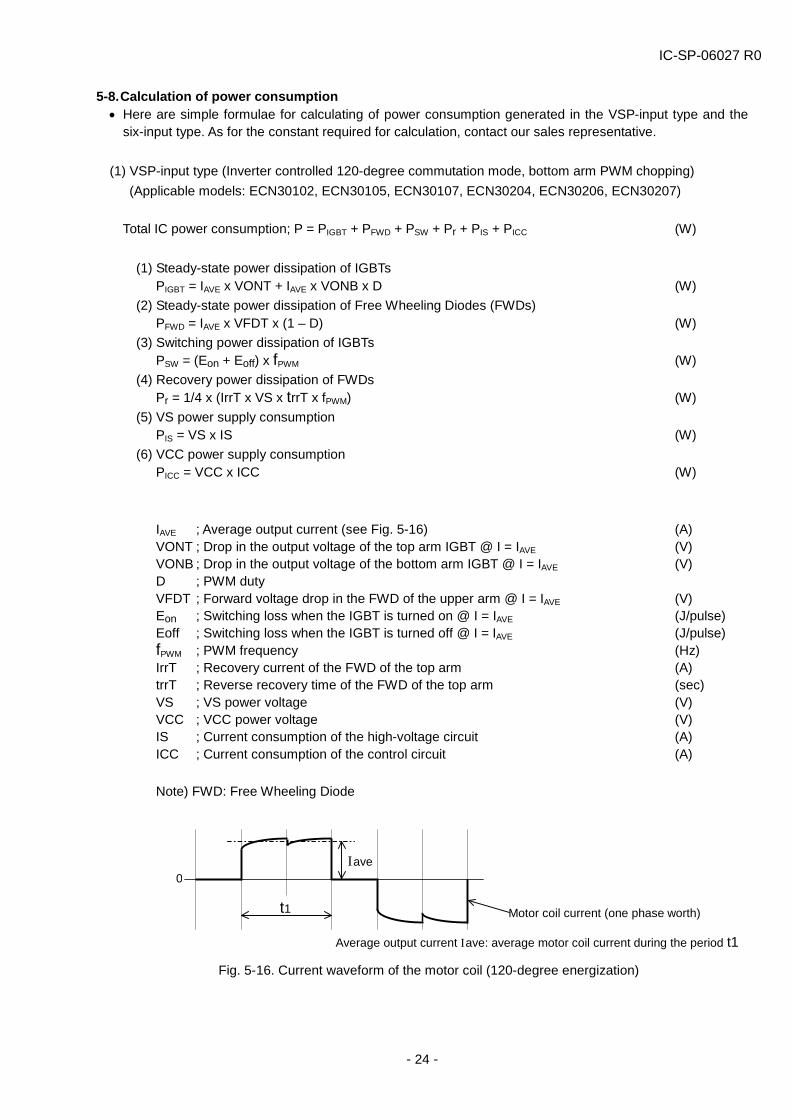
Fig. 5-16. Current waveform of the motor coil (120-degree energization)
Average output current Iave: average motor coil current during the period t1
0Iave
t1 Motor coil current (one phase worth)

IC-SP-06027 R0
- 25 -
(2) Six-input type (inverter controlled 180o sine wave commutation mode) (Applicable model: ECN30611, ECN30601, ECN30603, ECN30604) · The formula given below assumes the use of 180o sine wave commutation mode (all arms PWM
chopping).
Total IC power consumption; P = PIGBT + PFWD + PSW + Pr + PIS + PICC (W)
(1) Steady-state power dissipation of IGBTs PIGBT = IP x VONTP x (1/8 + D/3p x cosq) x 3 + IP x VONBP x (1/8 + D/3p x cosq) x 3 (W)
(2) Steady-state power dissipation of Free Wheeling Diodes (FWDs) PFWD = IP x VFDTP x (1/8 - D/3p x cosq) x 3 + IP x VFDBP x (1/8 - D/3p x cosq) x 3 (W)
(3) Switching power dissipation of IGBT PSW = (EonP +EoffP) x fPWM/p x 6 (W)
(4) Recovery power dissipation of FWDs Pr = 1/8 x (IrrT x VS x trrT x fPWM) x 3 + 1/8 x (IrrB x VS x trrB x fPWM) x 3 (W)
(5) VS power supply consumption PIS = VS x IS (W)
(6) VCC power supply consumption PICC = VCC x ICC (W)
IP ; Peak current (see Fig.5-17) (A) VONTP ; Drop in the output voltage of the top arm IGBT @ I = IP (V) VONBP ; Drop in the output voltage of the bottom arm IGBT @ I = IP (V) (1 + D x sin t)/2 ; PWM duty power factor during the time t cosq ; Power factor VFDTP ; Forward voltage drop in the FWD of the top arm @ I = IP (V) VFDBP ; Forward voltage drop in the FWD of the bottom arm @ I = IP (V) EonP ; Switching loss when the IGBT is turned on @ I = IP (J/pulse) EoffP ; Switching loss when the IGBT is turned off @ I = IP (J/pulse) fPWM ; PWM frequency (Hz) IrrT ; Recovery current of the FWD of the top arm (A) IrrB ; Recovery current of the FWD of the bottom arm (A) trrT ; Reverse recovery time of the FWD of the top arm (sec) trrB ; Reverse recovery time of the FWD of the bottom arm (sec) VS ; VS power voltage (V) VCC ; VCC power voltage (V) IS ; Current consumption of the high-voltage circuit (A) ICC ; Current consumption of the control circuit (A)
Note) FWD: Free Wheeling Diode
Fig.5-17. Current waveform of the motor coil (Inverter controlled 180o sine wave commutation mode)
0 Ip
Motor coil current (one phase worth)

IC-SP-06027 R0
- 26 -
(3) Calculation of junction temperature
A junction temperature can be calculated by the following equation after measuring the temperature of the IC case(Tab).
Tj = Tc + Rjc x P
Tj : Junction Temperature (oC) Tc : IC case(Tab) Temperature (oC) (actual measurement) Rjc : Thermal resistance of between junction and IC case (Tab) (oC/W) P : Total IC power consumption (W)
· Measuring method of Tc The thermo-couple is set in the tab of IC (heat sink) and temperature Tc of the IC case is measured. The temperature of Tc has the time dependency, please measure the temperature after it is saturated.
5-9. Derating
How much to derate a unit from the maximum rating is an important issue to consider a reliable design.
Items to be considered in the stage of system design include the derating of voltage, current, power, load, and electric stresses, along with the derating of temperature, humidity and other environmental conditions and vibration, impact and other mechanical stresses.
Table 5-7 specifies the standard examples of derating to be considered a reliable designing. To consider
these derating items in the stage of equipment design is desirable from the point of reliability securement. If any item is difficult to control within the standard, another means will be necessary, such as selecting a device having higher maximum ratings. Please consult our sales representative in advance.
Table 5-7. Typical derating design standards
Item Typical derating standards (example) Junction temperature Tj 110oC maximum
185V maximum ECN30102, ECN30105 ECN30107, ECN30611
VS power supply voltage 450V maximum
ECN30204, ECN30206, ECN30207 ECN30601, ECN30603, ECN30604
IC-SP-06027 R0
- 27 -
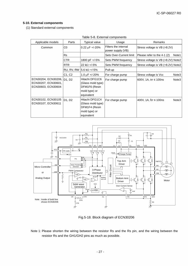
5-10. External components (1) Standard external components
Table 5-8. External components Applicable models Parts Typical value Usage Remarks
C0 0.22 mF +/-20% Filters the internal power supply (VB)
Stress voltage is VB (=8.2V)
Rs Sets Over-Current limit Please refer to the 4-1 (2) Note1
CTR 1800 pF +/-5% Sets PWM frequency Stress voltage is VB (=8.2V) Note2
RTR 22 kW +/-5% Sets PWM frequency Stress voltage is VB (=8.2V) Note2
RU, RV, RW 5.6 kW +/-5% Pull-up
Common
C1, C2 1.0 mF +/-20% For charge pump Stress voltage is Vcc Note3 ECN30204, ECN30206, ECN30207, ECN30601, ECN30603, ECN30604
D1, D2 Hitachi DFG1C6 (Glass mold type) DFM1F6 (Resin mold type) or equivalent
For charge pump 600V, 1A, trr ≤ 100ns Note3
ECN30102, ECN30105 ECN30107, ECN30611
D1, D2 Hitachi DFG1C4 (Glass mold type) DFM1F4 (Resin mold type) or equivalent
For charge pump 400V, 1A, trr ≤ 100ns Note3
Note 1: Please shorten the wiring between the resistor Rs and the Rs pin, and the wiring between the resistor Rs and the GH1/GH2 pins as much as possible.
Fig.5-18. Block diagram of ECN30206
Filte
r Circ
uit
CMP - +
CMP +
-
- +
PWM Comparator
VCC
VCC
Clock
GH1
Charge Pump
VS1 VS2
MU
MV
MW
CL
GL
VS
Clock
SAW wave Generator
VTR
D2 D1
C1 C2 +
+ - -
RTR
CTR
Over Current Sense
HU HW HV
CR
Vref
RS
RS
RU
RV
RW
Hall ICs
VSP
VCC VB
CB
C0 VCC(15V)
C+ C-
GH2
FG FG
DM
Note : Inside of bold line shows ECN30206
Bottom arm off
All off
Motor Bottom Arm
Driver
Top Arm Driver Motor Rotating
Direction Micro Controller
or Analog Output
LVSD
VB supply
3-Phase Distributor
IC-SP-06027 R0
- 28 -
Note 2: The PWM frequency is approximated by the following equation: PWM Frequency (in Hertz) @ 0.494 / ( CTR x RTR ) Note: CTR is in Farads, RTR is in Ohms.
· Please set the maximum frequency of PWM is 20KHz or less. · When the PWM frequency is set a high frequency, the switching loss is increased. And it
produces an increase in temperature of IC. · Please confirm the increased IC temperature with an actual set, and use it in the range of
derating curve.
Note 3: Attention of part setting of charge pump circuit The following attention is necessary when used excluding the standard part.
· When the voltage (Vcp) between C+ and C- is dropped, the gate voltage of top arm IGBTs is dropped. And then the loss of IC increases. Vcp must not become Vcp<10V.
Capacitor
· Vcp is dropped by the internal dissipation current from C+ terminal of IC, when capacity is small.
· The voltage impressed to the capacitor becomes VCC in operation. Therefore, the withstand voltage of the capacitor is necessary more than the VCC voltage.
Diode
· Forward voltage (VF) recommends the small one as much as possible. Because of, Vcp is dropped when VF is large.
· Reverse recovery time (trr) recommends the small one as much as possible. Because of, Reverse recovery charge (Qrr) becomes large at charge pump operation when trr is large. And then, VCP is drop.
· The withstand voltage of the diode is needed more than the VS voltage because CL is changed from about 0V to VS.
· The rush current flows to diode D1 and D2 by charging with capacitor C1 and C2 when the VCC power supply is turned on by VS=0V. Please select the ratings current of the diode in consideration of this current.
(2) Other external parts
· Parts of Table 5-9 are recommended to be arranged to protect stabilization and IC of the power supply from the voltage serge.
· Please adjust the part setting according to usage conditions. And also, please set up each part close to the terminal of IC to achieve the effect of the voltage serge absorption.
Table 5-9
Parts Purpose Remarks
Cvcc1 for High frequency noise suppressing Ceramic capacitor with good frequency response etc.
Cvcc2 for Vcc power supply smoothing Electrolytic capacitor etc.
ZDvcc for Over voltage suppressing Zener diode with good frequency response etc.
Cvs1 for High frequency noise suppressing Ceramic capacitor with good frequency response etc.
Cvs2 for Vs power supply smoothing Electrolytic capacitor etc.
ZDvs for Over voltage suppressing Zener diode with good frequency response etc.

IC-SP-06027 R0
- 29 -
6. Handling Instruction
6-1. Mounting (1) Insulation between pins
· High voltages are applied between the pins of the numbers specified below. Hitachi advises to apply coating or molding treatment.
1 - 2, 2 - 4, 6 - 7, 8 - 9, 9 - 10, 20 -21, 21- 22, 22 -23 · Coating resin comes in various types. There are some unclear points as to how much thermal and
mechanical stresses are exercised on semiconductor devices by size, thickness, and other factors of board shape, and the effects of other components. In selecting coating resin, please consult with your manufacturer.
(2) Connection of tabs (radiator panels of the ICs)
· Fig. 6-1 is a cross section of the IC. The tab and the GL pin of the IC are connected with high impedance (Rp = hundreds of KW to several MW).
· Set the tab potential to open or GND. · If the tab is mounted on the external cabinet of the motor for heat radiation purpose, the IC cannot
withstand an isolation withstand voltage test where a high voltage is applied between the external cabinet and the ground. Please apply a mylar sheet or something similar between the IC tab and the external cabinet.
Fig. 6-1. Cross section of Hiatchi HVIC
(3) Soldering conditions · Hitachi's inverter ICs (packages SP-23TA, SP-23TB, and SP-23TR) can be used in flow soldering* with
a peak temperature of less than 260oC and a dip time of no more than 10 seconds.
*: Flow soldering: The lead pin alone enters the solder basin, while the resin or tab does not.
Substrate
N
P N
Rp
To GL pin
To tab
Aluminum wire (SiO2) Isolation layer
N

IC-SP-06027 R0
- 30 -
6-2. Antistatic measures
· Containers and jigs for transporting ICs should be designed not to get charged under vibration or other impact during transportation. One effective measure is to use a conductive container or aluminum foil.
· Ground all work benches, machines and devices, meters, and other units that may get in contact with the ICs.
· While handling an IC, ground your body with a high resistor (about 100kW to 1MW) to prevent breakdown due to static electricity that has charged your body and/or clothes.
· Do not produce any friction with other polymer compounds. · To move any printed circuit board or other component equipped with an IC, make sure that no vibration or
friction occurs and short-circuit the pins to keep the potential at the same level. · Exercise control so that the humidity does not go too low. · Take enough care in handling to prevent the breakdown of ICs due to static electricity.
7. Quality
7-1. Quality tests
· Table 7-1 shows the main quality tests performed by our company.
Table 7-1 No. Test item Test conditions 1 High temperature operation VCC=VCCop, VS=Vsop, Tj=135oC, t=1000h 2 Motor rotation continuousness operation VCC=VCCop, VS=Vsop, Tj=135oC, t=1000h 3 High temperature storage Ta= 150oC, t=1000h 4 Low temperature storage Ta= -40oC, t=1000h 5 Temperature cycle -65oC to room temperature, 150oC,
100cycles (30min, 5min, 30min)
IC-SP-06027 R0
- 31 -
7-2. Quality Control Flow
Process Process ClassinficationFlow No. Process name
1 Sillicon Wafer incominginspection Wefer receive insupection
2 DI (dielectric isolation) DI condition
3 Photo lithography Photo lithographycondition
4 Diffusion Diffusion condition
5 Metal evaporation Metal evaporationcondition
6 Surface protection filmdeposition
Surface protection filmdeposition condition
7 Back grinding Grinding condition
8 Back metal evaporation Metal evaporationcondition
9 Wafer Probing Electrical characteristic
10 Assembling partsincoming inspection
Assembling parts receiveinspection
11 Dicing Dicing condition
12 Pellet appearance check Appearance
Control Item
11
10
12
9
1
2
3
4
5
6
7
8
Control MethodContents Sampling
ResistivityThickness Sampling
Appearance Size All
Pattern Form Sampling
Resistivity Gateoxidation thickness Sampling
ThicknessAppearance Sampling
ThicknessAppearance Sampling
Wafer thicknessAppearance Sampling
ThicknessAppearance Sampling
Electricalcharacteristic All
Appearance Size Sampling
Appearance Sampling
Appearance Sampling
Appearance Sampling
Remarks
[Process symbols] : Incoming : Inspection : Processing or machining
13 Die bonding Bonding condition
14 Joining Joining condition
15 Wire bonding Wire bonding condition
16 Molding Molding condition
17 Lead plating Lead plating condition
18 MarkingCutting bending
Marking conditionAppearance
19 Assembly finalappearance check Appearance
20 Screening CharacteristicAppearance
21 Final check CharacteristicAppearance
22 Store Checking
23 Shipping inspection Checking
24 Packing・Shipping Shipping guide
19
20
21
22
23
13
14
15
16
17
18
Appearance Sampling
Appearance Sampling
Appearance Sampling
Appearance Sampling
Appearance Sampling
Appearance Sampling
CharacteristicAppearance All
CharacteristicAppearance Size Sampling
Type The numberInventory code Sampling
Type The numberInventory code Sampling
- -
IC-SP-06027 R0
- 32 -
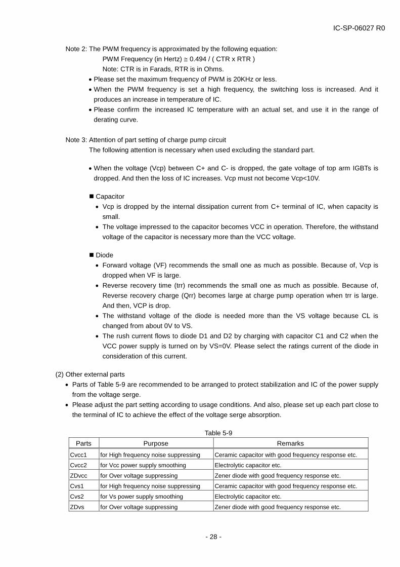
8. Inverter IC Handling Note 8-1. Electrical static destruction of VSP pin caused by external surge
Cause The external surge on the VSP line of the motor was put into IC directly.
Phenomenon The VSP signal is not transmitted in IC, and the motor doesn't rotate.
Countermeasure The series resistance is inserted so that the external surge is not put into IC directly. In addition, if capacitor is added, it becomes more effective.
Fig. 8-1. Example to configuration for external parts of VSP
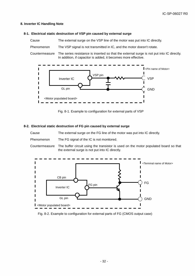
8-2. Electrical static destruction of FG pin caused by external surge
Cause The external surge on the FG line of the motor was put into IC directly.
Phenomenon The FG signal of the IC is not monitored.
Countermeasure The buffer circuit using the transistor is used on the motor populated board so that the external surge is not put into IC directly.
Fig. 8-2. Example to configuration for external parts of FG (CMOS output case)
Inverter IC VSP pin
GL pin GND
VSP
<Pin name of Motor>
<Motor populated board>
Inverter IC
CB pin
FG pin
GL pin GND
FG
<Terminal name of Motor>
<Motor populated board>
IC-SP-06027 R0
- 33 -
8-3. IC destruction by external surge inputted to VS and VCC line (1)
Cause The external surge on the VS and VCC line of the motor was put into IC. Because the Zener voltage of the surge suppressor diode was higher than the maximum rating voltage of IC, it did not protect IC.
Phenomenon The motor doesn't rotate by the over voltage destruction of IC.
Countermeasure Use the surge suppressor diode of the Zener voltage, which is lower than the
maximum rating voltage of IC.
8-4. IC destruction by external surge inputted to VS and VCC line (2)
Cause The external surge on the VS and VCC line of the motor was put into IC. Because the capacity of bypass capacitor for surge suppression was small, surge was not able to be suppressed enough.
Phenomenon The motor doesn't rotate by the over voltage destruction of IC.
Countermeasure Use the bypass capacitor for surge suppression, which capacity should be enough to
suppress surge.
Fig. 8-3. Example to surge waveform by difference of capacity of bypass capacitor
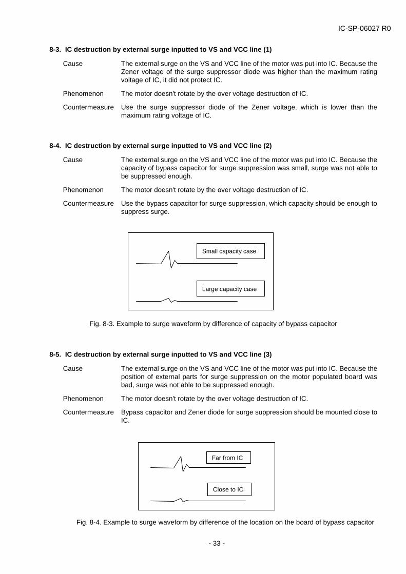
8-5. IC destruction by external surge inputted to VS and VCC line (3)
Cause The external surge on the VS and VCC line of the motor was put into IC. Because the position of external parts for surge suppression on the motor populated board was bad, surge was not able to be suppressed enough.
Phenomenon The motor doesn't rotate by the over voltage destruction of IC.
Countermeasure Bypass capacitor and Zener diode for surge suppression should be mounted close to
IC.
Fig. 8-4. Example to surge waveform by difference of the location on the board of bypass capacitor
Small capacity case
Large capacity case
Far from IC
Close to IC

IC-SP-06027 R0
- 34 -
8-6. IC destruction by line noise put into VCC (1)
Cause Pulsed noise of a voltage that is lower than LVSD level was put into VCC line of IC. In this case, IC repeats split-second LVSD operation. Then, IC will have the possibility of causing the overheating destruction.
Phenomenon The motor doesn't rotate by the overheating destruction of IC.
Countermeasure (1) The noise that is put into motor Vcc line is removed by reviewing the power supply
circuit(inductance and so on of power cable). (2) Suppress the noise by mounting the capacitor of enough capacity between Vcc
and GND pin of IC. That capacitor should be mounted close to Vcc-GND pin of IC.
Vcc = 15V VccL ≦ 10V TL @ 2ms
Fig. 8-5. Example to pulsed noise on Vcc at IC destruction
8-7. IC destruction by line noise put into VCC (2)
Cause The surge voltage that exceeds the maximum ratings of IC that was put into VCC pin of IC.
Phenomenon The motor doesn't rotate by the over voltage destruction of IC.
Countermeasure (1) Mount a bypass capacitor C1 close to pin of IC. It's effective to use a capacitor
that has excellent frequency characteristics, such as a ceramic capacitor, as a bypass capacitor. As a guide, ones of around 1mF are recommended (The larger the capacity, the more effective it is.).
(2) It is more effective to mount a surge suppression device such as bypass capacitor C2 close to connector of motor populated board like figure 8-6.
Fig. 8-6. Example to mount surge suppression devices
Vcc voltage level : Vcc
Noise level : VccL
Noise pulse width: TL
Detect voltage of LVSD: LVSDON
Motor Power supply cable
Vcc
Motor populated board Connector
V
Bypass Capacitor
C1 C2
IC
PCB
VCC pin
IC-SP-06027 R0
- 35 -
8-8. IC destruction by relay noise of inspection machine
Cause A mechanical relay for On-off control of electric connection between IC and inspection machine was used. Surge was generated when it was on-off, and it was put into IC.
Phenomenon The motor doesn't rotate by the over voltage destruction of IC.
Countermeasure Use the wet relay (mercury relay etc.). Confirm surge is not generated when the relay
is on-off.
Fig. 8-7 Example to surge waveform when mechanical relay is used
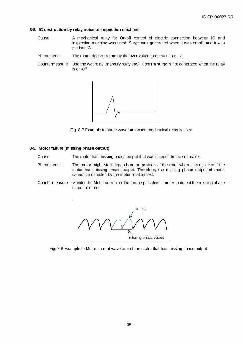
8-9. Motor failure (missing phase output)
Cause The motor has missing phase output that was shipped to the set maker.
Phenomenon The motor might start depend on the position of the rotor when starting even if the motor has missing phase output. Therefore, the missing phase output of motor cannot be detected by the motor rotation test.
Countermeasure Monitor the Motor current or the torque pulsation in order to detect the missing phase
output of motor.
Fig. 8-8 Example to Motor current waveform of the motor that has missing phase output
Normal
missing phase output
Related Documents