-P.1- Himax Confidential September, 2007 This information contained herein is the exclusive property of Himax and shall not be distributed, reproduced, or disclosed in whole or in part without prior written permission of Himax. ( DOC No. HX8238-A-DS ) HX8238-A 960 x 240 TFT LCD Single Chip Digital Driver Preliminary version 03 September, 2007

Welcome message from author
This document is posted to help you gain knowledge. Please leave a comment to let me know what you think about it! Share it to your friends and learn new things together.
Transcript

-P.1- Himax Confidential
September, 2007 This information contained herein is the exclusive property of Himax and shall not be distributed, reproduced, or disclosed in whole or in part without prior written permission of Himax.
( DOC No. HX8238-A-DS )
HX8238-A 960 x 240 TFT LCD Single Chip Digital Driver Preliminary version 03 September, 2007
This controller datasheet was downloaded from http://www.crystalfontz.com/controllers/Crystalfontz This controller datasheet was downloaded from http://www.crystalfontz.com/controllers/Crystalfontz

-P.1- Himax Confidential
September, 2007 This information contained herein is the exclusive property of Himax and shall not be distributed, reproduced, or disclosed in whole or in part without prior written permission of Himax.
1. General Description..................................................................................................................................... 5 2. Features ........................................................................................................................................................ 5 3. Block Diagram.............................................................................................................................................. 6 4. PAD Assignment .......................................................................................................................................... 7 5. Pin Description ............................................................................................................................................ 9 6. Block Function Description ...................................................................................................................... 12
6.1 Serial Interface ................................................................................................................................ 12 6.2 Data Control..................................................................................................................................... 14 6.3 Gamma/Grayscale Voltage Generator........................................................................................... 14 6.4 Boost and Regulator Circuit .......................................................................................................... 14 6.5 PWM Boost Converter .................................................................................................................... 14 6.6 Shift Register ................................................................................................................................... 14 6.7 Data Latches .................................................................................................................................... 14 6.8 Aging Mode...................................................................................................................................... 15 6.9 Reset Circuit .................................................................................................................................... 15
7. Command Table ......................................................................................................................................... 17 8. Command Description .............................................................................................................................. 18 9. OTP Programming ..................................................................................................................................... 32
10.1 Structure of Grayscale Amplifier ................................................................................................. 34 10.2 Gamma Adjustment Register....................................................................................................... 36
10.2.1 Gradient Adjusting Register ................................................................................................ 36 10.2.2 Amplitude Adjusting Register .............................................................................................. 36 10.2.3 Micro Adjusting Register ..................................................................................................... 36
10.3 Ladder Resistor / 8 to 1 Selector ................................................................................................. 37 11. Maximum Rating ...................................................................................................................................... 41 12. DC Characteristics................................................................................................................................... 42 13. AC Characteristics................................................................................................................................... 43 14. HX8238-A Output Voltage Relationship ................................................................................................. 56 15. Application Circuit ................................................................................................................................... 57 16. PAD Coordinate ....................................................................................................................................... 60 17. Ordering Information............................................................................................................................... 76 18. Revision History ...................................................................................................................................... 77
September, 2007
HX8238-A 960 x 240 TFT LCD Single Chip Digital Driver
List of Contents

-P.2- Himax Confidential This information contained herein is the exclusive property of Himax and shall not be distributed, reproduced, or disclosed in whole or in part without prior written permission of Himax. September, 2007
Figure 3. 1 HX8238-A Block Diagram Description ........................................................................... 6 Figure 4. 1 HX8238-A Die Floor Plan (Bump Face Up) ................................................................... 8 Figure 6. 1 SPI Timing.................................................................................................................... 13 Figure 8. 1 Status Read.................................................................................................................. 18 Figure 8. 2 Driver Output Control ................................................................................................... 18 Figure 8. 3 Scan Direction & Display ............................................................................................. 19 Figure 8. 4 LCD-Driving-Waveform Control ................................................................................... 19 Figure 8. 5 Power Control 1 ........................................................................................................... 19 Figure 8. 6 Input Data and Color Filter Control .............................................................................. 21 Figure 8. 7 Function control............................................................................................................ 23 Figure 8. 8 Contrast/Brightness Control......................................................................................... 24 Figure 8. 9 Frame Cycle Control .................................................................................................... 24 Figure 8. 10 NO Timing Diagram ................................................................................................... 24 Figure 8. 11 EQ Timing Diagram.................................................................................................... 25 Figure 8. 12 Power Control 2 ......................................................................................................... 25 Figure 8. 13 Power Control 3 ......................................................................................................... 27 Figure 8. 14 Gate Scan Position .................................................................................................... 27 Figure 8. 15 Gate scan display position ......................................................................................... 27 Figure 8. 16 Horizontal Porch......................................................................................................... 28 Figure 8. 17 Vertical Porch ............................................................................................................. 29 Figure 8. 18 No. of Clock Cycle of Clock ....................................................................................... 29 Figure 8. 19 No. of Clock Cycle of HSYNC.................................................................................... 30 Figure 8. 20 Power Control 4 ......................................................................................................... 30 Figure 8. 21 Gamma Control 1....................................................................................................... 31 Figure 8. 22 Gamma Control 2....................................................................................................... 31 Figure 9. 1 OTP Read Table........................................................................................................... 32 Figure 9. 2 OTP Programming Circuitry......................................................................................... 32 Figure 10. 1 Grayscale Control Block ............................................................................................ 33 Figure 10. 2 Grayscale Amplifier .................................................................................................... 34 Figure 10. 3 Resistor Ladder for Gamma Voltages Generation..................................................... 35 Figure 10. 4 Gamma Adjustment Function .................................................................................... 36
Figure13. 1 Pixel Timing................................................................................................................. 43 Figure13. 2 Data Transaction Timing in Parallel RGB (24 bit) Interface (SYNC Mode) ................ 44 Figure13. 3 Data Transaction Timing in Parallel RGB (24 bit) Interface (DE Mode) ..................... 45 Figure13. 4 Data Transaction Timing in Serial RGB (8 bit) Interface (SYNC Mode) ..................... 46 Figure13. 5 Data Transaction Timing in Serial RGB (8 bit) Interface (DE Mode) .......................... 47 Figure13. 6 Color Mode Conversion Timing .................................................................................. 47 Figure13. 7 CCIR601 Horizontal Timing ........................................................................................ 48 Figure13. 8 CCIR601 Vertical Timing............................................................................................. 49 Figure13. 9 CCIR656 Horizontal Timing ........................................................................................ 50 Figure13. 10 CCIR656 Vertical Timing........................................................................................... 51 Figure13. 11 Power Up Sequence ................................................................................................. 52 Figure13. 12 Power Down Sequence ............................................................................................ 53 Figure13. 13 SPI interface Timing Diagram & Write SPI Example ................................................ 54 Figure13. 14 SPI interface Timing Diagram & Read SPI Example................................................ 55 Figure13. 15Rising/Falling time...................................................................................................... 55
Figure 14. 1 LCD Driving Voltage Relationship ............................................................................. 56
HX8238-A 960 x 240 TFT LCD Single Chip Digital Driver
List of Figures September, 2007

-P.3- Himax Confidential This information contained herein is the exclusive property of Himax and shall not be distributed, reproduced, or disclosed in whole or in part without prior written permission of Himax. September, 2007
Figure 15. 1 Booster Capacitors .................................................................................................... 57 Figure 15. 2 Power Supply Pins Connections................................................................................ 57 Figure 15. 3 Filtering and Charge Sharing Capacitors................................................................... 58 Figure 15. 4 Panel and FPC Connection ....................................................................................... 58 Figure 15. 5 Panel Connection Example........................................................................................ 59
HX8238-A 960 x 240 TFT LCD Single Chip Digital Driver
List of Figures September, 2007

-P.4- Himax Confidential
September, 2007 This information contained herein is the exclusive property of Himax and shall not be distributed, reproduced, or disclosed in whole or in part without prior written permission of Himax.
Table 6. 1 R/S & R/W setting.......................................................................................................... 12 Table 6. 2 Registers Default Value................................................................................................. 16
Table 7. 1 Command Table............................................................................................................. 17 Table 8. 1 Source Output Level ...................................................................................................... 18 Table 8. 2 Step-up Cycle ................................................................................................................ 20 Table 8. 3 VGH and VGL Booster Ratio ......................................................................................... 20 Table 8. 4 Step-up Cycle ................................................................................................................ 21 Table 8. 5 Op-amp Power............................................................................................................... 21 Table 8. 6 Color Filter Type ............................................................................................................ 22 Table 8. 7 Interface Type ................................................................................................................ 22 Table 8. 8 Odd/Even Field Advanced Function .............................................................................. 22 Table 8. 9 Amount of Non-overlap.................................................................................................. 24 Table 8. 10 Delay Amount of Source Output .................................................................................. 24 Table 8. 11 EQ Period .................................................................................................................... 24 Table 8. 12 VLCD63 Voltage .......................................................................................................... 26 Table 8. 13 VCOM Amplitude ......................................................................................................... 27 Table 8. 14 No. of Pixel Per Line.................................................................................................... 28 Table 8. 15 No. of Clock Cycle of Clock ......................................................................................... 29 Table 8. 16 No. of Clock Cycle of HSYNC ..................................................................................... 30 Table 8. 17 VCOMH ....................................................................................................................... 31 Table 9. 1 OTP Programming Sequence ....................................................................................... 32 Table 10. 1 PRP (N) ....................................................................................................................... 37 Table 10. 2 VRP (N) 0 .................................................................................................................... 37 Table 10. 3 VRP (N) 1 .................................................................................................................... 37 Table 10. 4 PKP and PKN .............................................................................................................. 37 Table 10. 5 Grayscale Voltages Formulas ..................................................................................... 38 Table 10. 6 Reference Voltages of Positive Polarity ...................................................................... 39 Table 10. 7 Reference Voltages of Negative Polarity..................................................................... 40 Table 11. 1 Maximum Ratings ........................................................................................................ 41 Table 12. 1 DC Characteristics....................................................................................................... 42 Table 13. 1 Pixel Timing ................................................................................................................. 43 Table 13. 2 Data Transaction Timing in Normal Operating Mode.................................................. 45 Table 13. 3 Power Up Sequence.................................................................................................... 52 Table 13. 4 Power Down Sequence ............................................................................................... 53 Table 13. 5 SPI Timing ................................................................................................................... 55
HX8238-A 960 x 240 TFT LCD Single Chip Digital Driver
List of Tables September, 2007

-P.5-
September, 2007 This information contained herein is the exclusive property of Himax and shell not be distributed, reproduced, or disclosed in whole or in part without prior written permission of Himax.
Himax Confidential
1. General Description
The HX8238-A is a single chip controller and driver LSI that integrates the power circuit. It can drive a maximum 960x240 dot graphics on a-TFT panel displays in 262K colors. The HX8238-A has a low-voltage operation, 1.8 min voltage. In addition, The HX8238-A is equipped with a DC-DC converter control circuit that generates the supply voltage for source and gate drivers with minimum external components. A common voltage generation circuit is included to drive the TFT-display counter electrode. An integrated gamma control circuit is also included that can be adjusted by software commands to provide maximum flexibility and optimal display quality. The HX8238-A is suitable for any medium-sized or small portable battery-driven product requiring long-term driving capabilities, such as Digital Still Cameras.
2. Features
960 x 240 graphics display a-TFT panel controller/driver for 262K colors. Support digital 8-bits serial/24-bits parallel RGB and CCIR601/656 input mode. Power supply:
VDD = 1.8V – 2.50V (non-regulated input for logic) VDDIO = 1.8V – 3.60V (regulated input for logic) VCI = 2.50V – 3.60V (power supply for internal analog circuit)
Maximum gate driving output voltage: 30Vp-p Source driving output voltage: 0-5V Low current sleep mode and 8-color display mode for power saving. Display size: 960 x 240. Support Contrast/Brightness control Source and gate scan direction control. On-chip voltage generator. On-chip DC-DC converter up to 6x / -6x. Programmable gamma correction curve. Non-Volatile Memory (OTP) for VCOM calibration Programmable common electrode voltage amplitude and level for Cs on common
structure only PWM function to generate power for backlight control COG package
HX8238-A 960 x 240 TFT LCD Single Chip Digital Driver
Preliminary Version 03 September, 2007
-P.6- This information contained herein is the exclusive property of Himax and shell not be distributed, reproduced, or disclosed in whole or in part without prior written permission of Himax.
Himax Confidential
September, 2007
HX8238-A 960x 240 TFT LCD Single Chip Digital Driver
DATA SHEET Preliminary V03
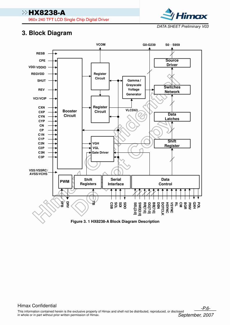
3. Block Diagram
ShiftRegister
BoosterCircuit
VDD/VDDIO
VCI/VCIP
CXN
REGVDD
SHUT
REV
Data
Latches
S0––––S959G0-G239
Switches
Network
SourceDriver
Register
CircuitCXP
CP
CYN
CYP
CN
C1N
C1P
C2N
C3N
C3P
VSS/VSSRC/AVSS/VCHS
Data
ControlShift
Registers
C2P
VCOM
TB CS
B
Serial
Interface
SC
L
SD
I
SD
O
RESB
RR
[7:0
]
GG
[7:0
]
BB
[7:0
]
DE
N
DO
TC
LK
HS
YN
C
VS
YN
C
RL
CM
BG
R
VGH
VGL
Gate Driver
Register
CircuitGamma /
Grayscale
Voltage
Generator
VLCD63
QX
H
PO
L
PWM
DR
V
VF
B
SE
L[2
:0]
SW
D[2
:0]
CPE
PIN
V
Figure 3. 1 HX8238-A Block Diagram Description

-P.7- This information contained herein is the exclusive property of Himax and shell not be distributed, reproduced, or disclosed in whole or in part without prior written permission of Himax.
Himax Confidential
September, 2007
HX8238-A 960x 240 TFT LCD Single Chip Digital Driver
DATA SHEET Preliminary V03
4. PAD Assignment THROUGH1 (1) THROUGH2 (1) DUMMY (1) DRV (2) VFB (2) DUMMY (1) VCHS (10) VSSRC (8) VCOM (4) VCOMH (4) VCOML (4) VCOMR (2) TEST16 (1) TEST17 (1) VGH (5) C3P (3) C3N (3) C2P (3) C2N (3) VGL (5) CP (3) CN (3) DUMMY (1) VDD (6) VCI (10) VCIP (4) VDDIO (6) CXP (6) CXN (6) CYP (6) CYN (6) VCIX2 (6) VCIX2J (6) VLCD63 (6) C1N (5) C1P (5) VCIM (5) DUMMY (1) PINV (1) CPE (1) VSS (1) SWD2 (1) VDDIO (1) SWD1 (1) VSS (1) SWD0 (1) VDDIO (1) SEL2 (1) SEL1 (1) SEL0 (1) VSS (1) BGR (1) VDDIO (1) CM (1) VSS (1) RL (1) VDDIO (1) REGVDD (1) VSS (1) REV (1) VDDIO (1) TB (1) VSS (1) SHUT (2) DOTCLK (2) VSYNC (2) HSYNC (2) DEN (2) RR7 (2) RR6 (2) RR5 (2) RR4 (2) RR3 (2) RR2 (2) RR1 (2) RR0 (2) GG7 (2) GG6 (2) GG5 (2) GG4 (2) GG3 (2) GG2 (2) GG1 (2) GG0 (2) BB7 (2) BB6 (2) BB5 (2) BB4 (2) BB3 (2) BB2 (2) BB1 (2) BB0 (2) SDI (2) SCK (2) CSB (2) RESB (2) SDO (2) POL (1) QXH (1) DUMMY (1) TEST4 (1) TEST5 (1) TEST6 (1) TEST7 (1) TEST8 (1) TEST9 (1) TEST10 (1) TEST11 (1) TEST12 (1) TEST13 (1) TEST14 (1) TEST15 (1) DUMMY (1) VSS (8) EXVR (4) AVSS (10) DUMMY (1) VCOM (4) DUMMY (1) THROUGH3 (1) THROUGH4 (1)
DUMMY (1) THROUGH5 (1) THROUGH6 (1) DUMMY (2) G1 G3 G5 G7 G235 G237 G237 G239 DUMMY (6) S0 S1 S2 S3 S955 S956 S957 S958 S959 DUMMY (9) G238 G236 G234 G232 G6 G4 G2 G0 DUMMY (2) THROUGH7 (1) THROUGH8 (1) DUMMY (1)

-P.8- This information contained herein is the exclusive property of Himax and shell not be distributed, reproduced, or disclosed in whole or in part without prior written permission of Himax.
Himax Confidential
September, 2007
HX8238-A 960x 240 TFT LCD Single Chip Digital Driver
DATA SHEET Preliminary V03
Alignment Marksymbo
lSize
Alignment mark size A 105um
Clearance gap 1 D 15um
Clearance gap 2 K 40um
Alignment mark width C 25um
Alignment area A x A 11025um^2
JH
C
A Input Padsymbo
lSize
Bump pitch A 75um
Bump width C 50um
Bump height H 110um
Bump gap1 (Vertical)
J 25um
Bump area C x H 5500um2
Output Padsymbo
lSize
Bump pitch A 18um
Bump width C 18um
Bump height H 100um
Bump gap1 (Vertical) J 30um
Bump gap2 (Horizontal) K 18um
Bump area C x H 1800um^2
A
C
J
H
K
Die Size approximately: 22180 x 970 um^2
Bump Height: 15 um +/- 3um
Bump Hardness: 60 Hv +/- 15 Hv
(10967.5, -145) (-10967.5, -145)
970 um
296
1520
Figure 4. 1 HX8238-A Die Floor Plan (Bump Face Up)
-P.9- This information contained herein is the exclusive property of Himax and shell not be distributed, reproduced, or disclosed in whole or in part without prior written permission of Himax.
Himax Confidential
September, 2007
HX8238-A 960x 240 TFT LCD Single Chip Digital Driver
DATA SHEET Preliminary V03
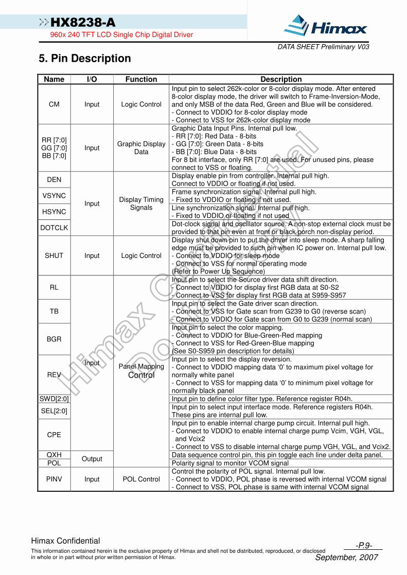
5. Pin Description
Name I/O Function Description
CM Input Logic Control
Input pin to select 262k-color or 8-color display mode. After entered 8-color display mode, the driver will switch to Frame-Inversion-Mode, and only MSB of the data Red, Green and Blue will be considered. - Connect to VDDIO for 8-color display mode - Connect to VSS for 262k-color display mode
RR [7:0] GG [7:0] BB [7:0]
Input Graphic Display
Data
Graphic Data Input Pins. Internal pull low. - RR [7:0]: Red Data - 8-bits - GG [7:0]: Green Data - 8-bits - BB [7:0]: Blue Data - 8-bits For 8 bit interface, only RR [7:0] are used. For unused pins, please connect to VSS or floating.
DEN Display enable pin from controller. Internal pull high. Connect to VDDIO or floating if not used.
VSYNC Frame synchronization signal. Internal pull high. - Fixed to VDDIO or floating if not used.
HSYNC Line synchronization signal. Internal pull high. - Fixed to VDDIO or floating if not used
DOTCLK
Input Display Timing
Signals
Dot-clock signal and oscillator source. A non-stop external clock must be provided to that pin even at front or black porch non-display period.
SHUT Input Logic Control
Display shut down pin to put the driver into sleep mode. A sharp falling edge must be provided to such pin when IC power on. Internal pull low. - Connect to VDDIO for sleep mode - Connect to VSS for normal operating mode (Refer to Power Up Sequence)
RL Input pin to select the Source driver data shift direction. - Connect to VDDIO for display first RGB data at S0-S2 - Connect to VSS for display first RGB data at S959-S957
TB Input pin to select the Gate driver scan direction. - Connect to VSS for Gate scan from G239 to G0 (reverse scan) - Connect to VDDIO for Gate scan from G0 to G239 (normal scan)
BGR
Input pin to select the color mapping. - Connect to VDDIO for Blue-Green-Red mapping - Connect to VSS for Red-Green-Blue mapping (See S0-S959 pin description for details)
REV
Input pin to select the display reversion. - Connect to VDDIO mapping data ‘0’ to maximum pixel voltage for normally white panel - Connect to VSS for mapping data ‘0’ to minimum pixel voltage for normally black panel
SWD[2:0] Input pin to define color filter type. Reference register R04h.
SEL[2:0] Input pin to select input interface mode. Reference registers R04h. These pins are internal pull low.
CPE
Input
Input pin to enable internal charge pump circuit. Internal pull high. - Connect to VDDIO to enable internal charge pump Vcim, VGH, VGL, and Vcix2 - Connect to VSS to disable internal charge pump VGH, VGL, and Vcix2.
QXH Data sequence control pin, this pin toggle each line under delta panel.
POL Output
Panel Mapping
Control
Polarity signal to monitor VCOM signal
PINV Input POL Control Control the polarity of POL signal. Internal pull low. - Connect to VDDIO, POL phase is reversed with internal VCOM signal - Connect to VSS, POL phase is same with internal VCOM signal

-P.10- This information contained herein is the exclusive property of Himax and shell not be distributed, reproduced, or disclosed in whole or in part without prior written permission of Himax.
Himax Confidential
September, 2007
HX8238-A 960x 240 TFT LCD Single Chip Digital Driver
DATA SHEET Preliminary V03
Name I/O Function Description
REGVDD Input Logic Control
Input pin to enable internal voltage regulation. -Connect to VDDIO if System Vdd > 2.5V
-Connect to VSS if 2.5V ≥ System Vdd ≥ 1.8V, internal regulator will be disabled
RESB Input System Reset System reset pin. Internal pull high. - Connect to VDDIO when not used (Refer to Power Up Sequence)
CSB Chip select pin of serial interface. Internal pull high. - Leave it OPEN when not used (Refer to Serial Interface block)
SCK Clock pin of serial interface. Internal pull high. - Leave it OPEN when not used (Refer to Serial Interface block)
SDI
Input
Data input pin in serial mode. Internal pull high. - Leave it OPEN when not used (Refer to Serial Interface block)
SDO Output
Serial Interface
Data output pin in serial mode. - Leave it OPEN when not used (Refer to Serial Interface block)
VDDIO Voltage input pin for I/O logic. - Connect to system Vdd
VDD
Power Power Supply for
Logic Circuits
Voltage input pin for internal logic. a) REGVDD = VDDIO
Internal regulator will be on for 3.6V ≥ System Vdd ≥ 2.5V VDD ~2V. b) REGVDD = VSS
Internal regulator will be off for 2.5V ≥ System Vdd ≥ 1.8V VDD = System Vdd
VSS System ground pin of the IC. - Connect to system ground
AVSS Grounding for analog circuit. - Connect to system ground
VSSRC Grounding for analog circuit. This pin requires a noise free path for providing accurate LCD driving voltages. - Connect to system ground.
VCHS
Power Ground of the Power Supply
Grounding for booster circuit. - Connect to system ground.
VCI Booster input voltage pin. - Connect to voltage source between 2.5V to 3.6V
VCIP
Power Power Supply for Analog Circuits
Voltage supply pin for analog circuit. This pin requires a noise free path for providing accurate LCD driving voltages. - Connect to same source of VCI
VCIM Negative voltage of VCI. - Connect a capacitor for stabilization
VCIX2
Output Booster Voltages Equals to 2 x VCI. - Connect a capacitor for stabilization
VCIX2J Power Voltage for
Analog This is the power supply used by on chip analog blocks and VGH/VGL dcdc.
EXVR External reference of internal Gamma resistor. - Connect to VSS
VCOMR
Input External
Reference This pin provides voltage reference for internal voltage regulator when register VDV [6:0] of Power Control 3 set to “01111XX”. - Connect to an external voltage source for reference
VCOMH This pin indicates a HIGH level of VCOM generated in driving the VCOM alternation. - Connect a capacitor for stabilization
VCOML
Output Voltages for
VCOM Signal This pin indicates a LOW level of VCOM generated in driving the VCOM alternation. - Connect a capacitor for stabilization
-P.11- This information contained herein is the exclusive property of Himax and shell not be distributed, reproduced, or disclosed in whole or in part without prior written permission of Himax.
Himax Confidential
September, 2007
HX8238-A 960x 240 TFT LCD Single Chip Digital Driver
DATA SHEET Preliminary V03
Name I/O Function Description
VLCD63 Internal generated power for source driver - Connect a capacitor for stabilization
VGH A positive power output pin for gate driver. - Connect a capacitor for stabilization
VGL
Output LCD Driving
Voltages
A negative power output pin for gate driver. - Connect a capacitor for stabilization
CP - Connect a capacitor to CN
CXP - Connect a capacitor to CXN
CYP - Connect a capacitor to CYN
C1P - Connect a capacitor to C1N
C2P - Connect a capacitor to C2N
C3P - Connect a capacitor to C3N
CN - Connect a capacitor to CP
CXN - Connect a capacitor to CXP
CYN - Connect a capacitor to CYP
C1N - Connect a capacitor to C1P
C2N - Connect a capacitor to C2P
C3N
Input Booster and Stabilization Capacitors
- Connect a capacitor to C3P
DRV Output Power transistor gate signal for the boost converter
VFB Input PWM control
Main boost regulator feedback input. Connect feedback resistive divider to GND. FB threshold is 0.6 V nominal
TEST4~5 Input IC Testing Signal Test pin of the internal circuit. Leave it connect to ground.
TEST6~17 Output IC Testing Signal Test pin of the internal circuit. Leave it OPEN.
VCOM A power supply for the TFT-display common electrode.
G0-G239 Gate driver output pins. These pins output VGH, VGL level.
S0-S959
Output LCD Driving
Signals Source driver output pins. S (3n): display Red if BGR = LOW, Blue if BGR = HIGH. S (3n+1): display Green. S (3n+2): display Blue if BGR = LOW, Red if BGR = HIGH.
THROUGH1
THROUGH2
Dummy pads. Used to measure the COG contact resistance. These two pins are short circuited within the chip
THROUGH3
THROUGH4
Dummy pads. Used to measure the COG contact resistance. These two pins are short circuited within the chip
THROUGH5
THROUGH6
Dummy pads. Used to measure the COG contact resistance. These two pins are short circuited within the chip
THROUGH7
THROUGH8
- -
Dummy pads. Used to measure the COG contact resistance. These two pins are short circuited within the chip
DUMMY - - Floating pins and no connection inside the IC. These pins can be shorted together or connect to any signal.

-P.12- This information contained herein is the exclusive property of Himax and shell not be distributed, reproduced, or disclosed in whole or in part without prior written permission of Himax.
Himax Confidential
September, 2007
HX8238-A 960x 240 TFT LCD Single Chip Digital Driver
DATA SHEET Preliminary V03
6. Block Function Description
6.1 Serial Interface
The SPI is available through the chip select line (CSB), serial transfer clock line (SCK), serial data input (SDI), and serial data output (SDO). The Driver IC recognizes the start of data transfer at the falling edge of CSB input to initiate the transfer of start byte. It recognizes the end of data transfer at the rising edge of CSB input. The Driver IC is selected when the 6-bit chip address in the start byte transferred from the transmission device and the 6-bit device identification code assigned to the Driver IC are compared and both 6-bit data correspond. The identification code must be 011100. Two different chip addresses must be assigned to the Driver IC because the seventh bit of the start byte is assigned to a register select bit (R/S). When R/S = 0, index register write or status read is executed. When the R/S = 1, instruction write. The eighth bit of the start byte is to specify read or write (R/W bit). The data are received when the R/W bit is 0, and are transmitted when the R/W bit is 1. After receiving the start byte, the Driver IC starts to transmit or receive data by byte. The data transmission adopts a format by which the MSB is firt transmitted (9th SCK started). All Driver IC instructions consist of 16 bits and they are executed internally after two bytes are transmitted with the MSB first (IB15 to 0---9th ~24th SCK).
R/S R/W status 0 0 Write SPI address 0 1 Read gate line number (Note) 1 0 Write SPI data 1 1 Read SPI data
Note: this function could let user know which gate line was turned on at that time.
Table 6. 1 R/S & R/W setting
-P.13- This information contained herein is the exclusive property of Himax and shell not be distributed, reproduced, or disclosed in whole or in part without prior written permission of Himax.
Himax Confidential
September, 2007
HX8238-A 960x 240 TFT LCD Single Chip Digital Driver
DATA SHEET Preliminary V03
1 2 3 4 5 6 7 8 9 10 11 12 13 14 15 16 17 18 19 20 21 22 23 24
0 R/S R/W
CSB
SCK
SDI 1 1 1 DB
15DB14
DB13
DB12
DB11
DB10
DB9
DB
8
DB7
DB
6
DB5
DB4
DB3
DB2
DB1
DB0
00
MSB LSB
DB15
DB14
DB13
DB12
DB11
DB10
DB9
DB8
DB7
DB6
DB5
DB4
DB3
DB2
DB1
DB0
Device ID Index register setting/Instruction
Status read
SDO
Transfer starts Transfer ends
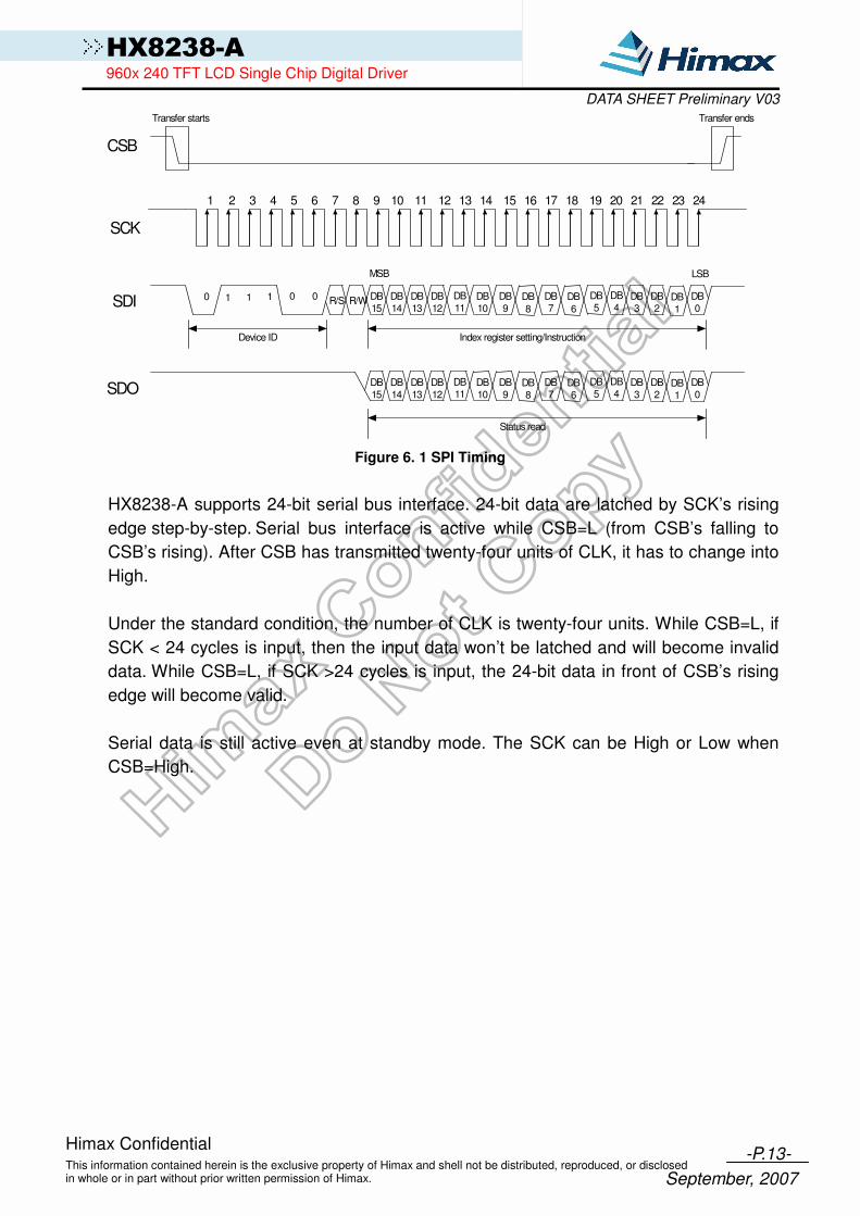
Figure 6. 1 SPI Timing
HX8238-A supports 24-bit serial bus interface. 24-bit data are latched by SCK’s rising
edge step-by-step. Serial bus interface is active while CSB=L (from CSB’s falling to
CSB’s rising). After CSB has transmitted twenty-four units of CLK, it has to change into
High.
Under the standard condition, the number of CLK is twenty-four units. While CSB=L, if
SCK < 24 cycles is input, then the input data won’t be latched and will become invalid
data. While CSB=L, if SCK >24 cycles is input, the 24-bit data in front of CSB’s rising
edge will become valid.
Serial data is still active even at standby mode. The SCK can be High or Low when
CSB=High.

-P.14- This information contained herein is the exclusive property of Himax and shell not be distributed, reproduced, or disclosed in whole or in part without prior written permission of Himax.
Himax Confidential
September, 2007
HX8238-A 960x 240 TFT LCD Single Chip Digital Driver
DATA SHEET Preliminary V03
6.2 Data Control
The display data and frame position information from the controller is synchronized with the Gate Drive circuit and shift registered for the Source Driver circuit.
6.3 Gamma/Grayscale Voltage Generator
The grayscale voltage circuit generates a LCD driver circuit that corresponds to the grayscale levels as specified in the grayscale gamma-adjusting resistor. 262K possible colors can be displayed.
6.4 Boost and Regulator Circuit
These two functional blocks generate the voltage of VGH, VGL, VCOMH, VCOML and VLCD63, which are necessary for operating a TFT LCD.
6.5 PWM Boost Converter
PWM Boost Converter
PWM Controller
0.6V
-
+
L1
D1
R2
R1
C2
VCC
VO
DRV
VFB
The internal reference voltage is adjustable by FB [2:0] in R05h. By adjusting the voltage, you can get different VO to meet your system application.
6.6 Shift Register
The shift registers control the direction of line scanning of source.
6.7 Data Latches
This block is a series of latches carrying the display signal information. These latches hold the data, which will be fed to the Source Driver to output the required voltage level.

-P.15- This information contained herein is the exclusive property of Himax and shell not be distributed, reproduced, or disclosed in whole or in part without prior written permission of Himax.
Himax Confidential
September, 2007
HX8238-A 960x 240 TFT LCD Single Chip Digital Driver
DATA SHEET Preliminary V03
6.8 Aging Mode If only DOTCLK is sent into driver IC without VSYNC, HSYNC, and DEN signals, HX8238-A will enter Aging Mode after power on. In Aging Mode, the display will show Black, White, Red, Green, and Blue images in series automatically.
6.9 Reset Circuit
This block is integrated into the Interface Logic which includes Power On Reset circuitry and the hardware reset pin, /RES. Both of these having the same reset function. Once the /RES pin receives a negative reset pulse, all internal circuitry will start to initialize. The minimum pulse width for completing the reset sequence is 10us. The status of the chip after reset is given by:

-P.16- This information contained herein is the exclusive property of Himax and shell not be distributed, reproduced, or disclosed in whole or in part without prior written permission of Himax.
Himax Confidential
September, 2007
HX8238-A 960x 240 TFT LCD Single Chip Digital Driver
DATA SHEET Preliminary V03
Reg# Hex
Code Register Bit Value
R01h XX00 RL = X REV = X PINV = X BGR = X SM = “0” TB = X CPE = X
R02h 0200 B/C = “1”
R03h 6364 DCT = “0110” BT = “011” BTF = “0” DC = “0110” AP = “010”
R04h 04XX PALM = “1” BLT = ”00” OEA = Note(2) SEL = X SWD = X
R05h GHN=”1” XDK=”0” GDIS=”1” LPF=”1” DEP=”0” CKP=”1” VSP= Note
(2) HSP=”0” DEO=”1” DIT=”1” PWM=”0” FB=”100”
R0Ah 4008 BR = “1000000” CON = “01000”
R0Bh D400 NO = “11” SDT = “01” EQ = “100”
R0Dh 3229 VRC = “011” VDS = “10” VRH = “101001”
R0Eh 3200 VDV = “1001000”
R0Fh 0000 SCN = “00000000”
R16h 9F80 XLIM = “100111111”
R17h STH = “00” HBP = Note(2) VBP = Note
(2)
R1Eh 0052 nOTP = “0” VCM = “1010010”
R30h 0000 PKP1 = “000” PKP0 = “000”
R31h 0407 PKP3 = “100” PKP2 = “111”
R32h 0202 PKP5 = “010” PKP4 = “010”
R33h 0000 PRP1 = “000” PRP0 = “000”
R34h 0505 PKN1 = “101” PKN0 = “101”
R35h 0003 PKN3 = “000” PKN2 = “011”
R36h 0707 PKN5 = “111” PKN4 = “111”
R37h 0000 PRN1 = “000” PRN0 = “000”
R3Ah 0904 VRP1 = “01001” VRP0 = “0100”
R3Bh 0904 VRN1 = “01001” VRN0 = “0100”
Note: (1) X means the bit is refer to the logic stage of the corresponding hardware pin. (2) The default values of the VSP、OEA、HBP、VBP are automatically set by SEL.
Table 6. 2 Registers Default Value

-P.17- This information contained herein is the exclusive property of Himax and shell not be distributed, reproduced, or disclosed in whole or in part without prior written permission of Himax.
Himax Confidential
September, 2007
HX8238-A 960x 240 TFT LCD Single Chip Digital Driver
DATA SHEET Preliminary V03
7. Command Table
Reg# Register R/W R/S IB15 IB14 IB13 IB12 IB11 IB10 IB9 IB8 IB7 IB6 IB5 IB4 IB3 IB2 IB1 IB0
SR Status Read 1 0 L7 L6 L5 L4 L3 L2 L1 L0 0 0 0 0 0 0 0 0
R01h Driver output
control 0 1 0 RL REV PINV BGR SM TB CPE 0 0 0 0 0 0 0 0
R02h LCD driver AC control
0 1 0 0 0 0 0 0 B/C 0 0 0 0 0 0 0 0 0
R03h Power
control (1) 0 1 DCT3 DCT2 DCT1 DCT0 BTF BT2 BT1 BT0 DC3 DC2 DC1 DC0 AP2 AP1 AP0 0
R04h Data and color filter
control 0 1 0 0 0 0 0 PALM BLT1 BLT0 OEA1 OEA0 SEL2 SEL1 SEL0 SWD2 SWD1 SWD0
R05h Function control
0 1 GHN XDK GDIS LPF DEP CKP VSP HSP DEO DIT 0 PWM 0 FB2 FB1 FB0
R06h Reserved Reserved
R07h Reserved Reserved
R0Ah Contrast/
Brightness control
0 1 0 BR6 BR5 BR4 BR3 BR2 BR1 BR0 0 0 0 CON4 CON3 CON2 CON1 CON0
R0Bh Frame cycle
control 0 1 NO1 NO0 SDT1 SDT0 0 EQ2 EQ1 EQ0 0 0 0 0 0 0 0 0
R0Dh Power
control (2) 0 1 0 VRC2 VRC1 VRC0 0 0 VDS1 VDS0 0 0 VRH5 VRH4 VRH3 VRH2 VRH1 VRH0
R0Eh Power
control (3) 0 1 0 0 1 VDV6 VDV5 VDV4 VDV3 VDV2 VDV1 VDV0 0 0 0 0 0 0
R0Fh Gate scan
starting Position
0 1 0 0 0 0 0 0 0 0 SCN7 SCN6 SCN5 SCN4 SCN3 SCN2 SCN1 SCN0
R16h Horizontal
Porch 0 1 XLIM8 XLIM7 XLIM6 XLIM5 XLIM4 XLIM3 XLIM2 XLIM1 XLIM0 0 0 0 0 0 0 0
R17h Vertical Porch
0 1 STH1 STH0 HBP6 HBP5 HBP4 HBP3 HBP2 HBP1 HBP0 VBP6 VBP5 VBP4 VBP3 VBP2 VBP1 VBP0
R1Eh Power
control (4) 0 1 0 0 0 0 0 0 0 0 nOTP VCM6 VCM5 VCM4 VCM3 VCM2 VCM1 VCM0
R27h Reserved Reserved
R28h Reserved Reserved
R29h Reserved Reserved
R2Bh Reserved Reserved
R30h γ control (1) 0 1 0 0 0 0 0 PKP 12
PKP 11
PKP 10
0 0 0 0 0 PKP 02
PKP 01
PKP 00
R31h γ control (2) 0 1 0 0 0 0 0 PKP 32
PKP 31
PKP 30
0 0 0 0 0 PKP 22
PKP 21
PKP 20
R32h γ control (3) 0 1 0 0 0 0 0 PKP 52
PKP 51
PKP 50
0 0 0 0 0 PKP 42
PKP 41
PKP 40
R33h γ control (4) 0 1 0 0 0 0 0 PRP 12
PRP 11
PRP 10
0 0 0 0 0 PRP 02
PRP 01
PRP 00
R34h γ control (5) 0 1 0 0 0 0 0 PKN 12
PKN 11
PKN 10
0 0 0 0 0 PKN 02
PKN 01
PKN 00
R35h γ control (6) 0 1 0 0 0 0 0 PKN 32
PKN 31
PKN 30
0 0 0 0 0 PKN 22
PKN 21
PKN 20
R36h γ control (7) 0 1 0 0 0 0 0 PKN 52
PKN 51
PKN 50
0 0 0 0 0 PKN 42
PKN 41
PKN 40
R37h γ control (8) 0 1 0 0 0 0 0 PRN 12
PRN 11
PRN 10
0 0 0 0 0 PRN 02
PRN 01
PRN 00
R3Ah γ control (9) 0 1 0 0 0 VRP
14 VRP 13
VRP 12
VRP 11
VRP 10
0 0 0 0 VRP 03
VRP 02
VRP 01
VRP 00
R3Bh γ control (10) 0 1 0 0 0 VRN
14 VRN 13
VRN 12
VRN 11
VRN 10
0 0 0 0 VRN 03
VRN 02
VRN 01
VRN 00
Note: * means don’t care Software settings will override hardware pin (eg, BGR bits override BGR pin definition)
Table 7. 1 Command Table

-P.18- This information contained herein is the exclusive property of Himax and shell not be distributed, reproduced, or disclosed in whole or in part without prior written permission of Himax.
Himax Confidential
September, 2007
HX8238-A 960x 240 TFT LCD Single Chip Digital Driver
DATA SHEET Preliminary V03
8. Command Description Status Read
R/W R/S IB15 IB14 IB13 IB12 IB11 IB10 IB9 IB8 IB7 IB6 IB5 IB4 IB3 IB2 IB1 IB0
R 0 L7 L6 L5 L4 L3 L2 L1 L0 0 0 0 0 0 0 0 0
Figure 8. 1 Status Read
The status read instruction reads the internal status of the HX8238-A. L7–0: Indicate the driving raster-row position where the liquid crystal display is being
driven.
Driver Output Control (R01h) R/W R/S IB15 IB14 IB13 IB12 IB11 IB10 IB9 IB8 IB7 IB6 IB5 IB4 IB3 IB2 IB1 IB0 W 1 0 R L REV PINV BGR S M T B CPE 0 0 0 0 0 0 0 0
Figure 8. 2 Driver Output Control
CPE: When CPE=0, Vcim is not shut down, but VGH, VGL, and Vcix2 are shut down. When CPE=1, internal charge pump Vcim, VGH, VGL, and Vcix2 are enabled.
REV: Displays all character and graphics display sections with reversal when REV = “0”. Since the grayscale level can be reversed, display of the same data is enabled on normally white and normally black panels. Source output level is indicated below.
Source output level REV RGB data VCOM = ”L” VCOM = ”H”
1 00000H
: 3FFFFH
V0 :
V63
V63 :
V0
0 00000H
: 3FFFFH
V63 :
V0
V0 :
V63
Table 8. 1 Source Output Level
PINV: When PINV=0, POL output is same phase with internal VCOM signal. When PINV=1, POL output phase is reversed with VCOM signal.
BGR: Selects the <R><G><B> arrangement. When BGR = “0” <R><G><B> color is assigned from S0.When BGR = “1” <B><G><R> color is assigned from S0.
SM: Change the division of gate driver. When SM = “0”, odd/even division (interlace mode) is selected. When SM = “1”, upper/lower division is selected. Select the division mode according to the mounting method.
TB: Selects the output shift direction of the gate driver. When TB = “1”, G0 shifts to G239. When TB = “0”, G239 shifts to G0.
RL: Selects the output shift direction of the source driver. When RL = “1”, S0 shifts to S959 and <R><G><B> color is assigned from S0. When RL = “0”, S959 shifts to S0 and <R><G><B> color is assigned from S959. Set RL bit and BGR bit when changing the dot order of R, G and B.
Note: The default setting of register bits REV, BGR, TB and RL are defined by the logic stage of corresponding hardware
pins. These bits will override the hardware setting once software command was sent to set the bits.

-P.19- This information contained herein is the exclusive property of Himax and shell not be distributed, reproduced, or disclosed in whole or in part without prior written permission of Himax.
Himax Confidential
September, 2007
HX8238-A 960x 240 TFT LCD Single Chip Digital Driver
DATA SHEET Preliminary V03
SM = 0 SM = 1
TB = 1
RL = 1
G0
S0 S959
G2
G4
G1
G3
G5
G237
G239
G236
G238
G0
S959S0
G2G4
G1G3G5
G237G239
G236G238
TB = 0
RL = 1 236
238
G0
S959S0
G2
G4
G1
G3
G5
G237
G239
G
G
G0
S959S0
G2G4
G1G3G5
G237G239
G236G238
TB = 1
RL = 0
G0
S959S0
G2
G4
G1
G3
G5
G237
G239
G236
G238
G0
S959S0
G2G4
G1G3G5
G237G239
G236G238
TB = 0
RL = 0
G0
S959S0
G2
G4
G1
G3
G5
G237
G239
G236
G238
G0
S959S0
G2G4
G1G3G5
G237G239
G236G238
Figure 8. 3 Scan Direction & Display
LCD-Driving-Waveform Control (R02h) R/W R/S IB15 IB14 IB13 IB12 IB11 IB10 IB9 IB8 IB7 IB6 IB5 IB4 IB3 IB2 IB1 IB0
W 1 0 0 0 0 0 0 B / C 0 0 0 0 0 0 0 0 0
Figure 8. 4 LCD-Driving-Waveform Control
B/C: When B/C = 0, frame inversion of the LCD driving signal is enabled. When B/C = 1, line inversion waveform is generated
Power control 1 (R03h)
R/W R/S IB15 IB14 IB13 IB12 IB11 IB10 IB9 IB8 IB7 IB6 IB5 IB4 IB3 IB2 IB1 IB0
W 1 DCT3 DCT2 DCT1 DCT0 BTF BT2 BT1 BT0 DC3 DC2 DC1 DC0 AP2 AP1 AP0 0
Figure 8. 5 Power Control 1

-P.20- This information contained herein is the exclusive property of Himax and shell not be distributed, reproduced, or disclosed in whole or in part without prior written permission of Himax.
Himax Confidential
September, 2007
HX8238-A 960x 240 TFT LCD Single Chip Digital Driver
DATA SHEET Preliminary V03
DCT3-0: Set the step-up cycle of the step-up circuit for 8-color mode (CM = VDDIO). When the cycle is accelerated, the Vcim and Vcix2 driving ability of the step-up circuit increase, but their current consumption increase, too. Adjust the cycle taking into account the display quality and power consumption.
VGH and VGL are always fixed at the step-up cycle of Fline x 0.5.
DCT3 DCT2 DCT1 DCT0 Step-up cycle
0 0 0 0 Fline x 14 0 0 0 1 Fline x 12 0 0 1 0 Fline x 10 0 0 1 1 Fline x 8 0 1 0 0 Fline x 7 0 1 0 1 Fline x 6 0 1 1 0 Fline x 5 0 1 1 1 Fline x 4 1 0 0 0 Fline x 3 1 0 0 1 Fline x 2 1 0 1 0 Fline x 1 1 0 1 1 Fline x 0.5 1 1 0 0 Fline x 0.25 1 1 0 1 Reserved 1 1 1 0 Reserved 1 1 1 1 Reserved
* Fline = horizontal frequency (Fline Typ. 15KHz)
Table 8. 2 Step-up Cycle
BT2-0 & BTF: Control the step-up factor of the step-up circuit. Adjust the step-up factor according to the power supply voltage to be used.
BTF BT2 BT1 BT0 VGH output VGL output
0 0 0 0 VCIX2j X 3 - (VCIX2j X 3) + VCI
0 0 0 1 VCIX2j X 3 - (VCIX2j X 2)
0 0 1 0 VCIX2 j X 3 - (VCIX2j X 3)
0 0 1 1 VCIX2j X 2 + VCI - (VCIX2j X 2) - VCI
0 1 0 0 VCIX2j X 2 + VCI - (VCIX2j X 2)
0 1 0 1 VCIX2j X 2 + VCI - (VCIX2j X 2) + VCI
0 1 1 0 VCIX2j X 2 - (VCIX2j X 2)
0 1 1 1 VCIX2j X 2 - (VCIX2j X 2) + VCI
1 X X X VCIX2j X 3 - VCIX2j
Table 8. 3 VGH and VGL Booster Ratio

-P.21- This information contained herein is the exclusive property of Himax and shell not be distributed, reproduced, or disclosed in whole or in part without prior written permission of Himax.
Himax Confidential
September, 2007
HX8238-A 960x 240 TFT LCD Single Chip Digital Driver
DATA SHEET Preliminary V03
DC3-0: Set the step-up cycle of the step-up circuit for 262k-color mode (CM = VSS). When the cycle is accelerated, the Vcim and Vcix2 driving ability of the step-up circuit increase, but their current consumption increase, too. Adjust the cycle taking into account the display quality and power consumption.
VGH and VGL are always fixed at the step-up cycle of Fline x 0.5.
DC3 DC2 DC1 DC0 Step-up cycle
0 0 0 0 Fline x 14 0 0 0 1 Fline x 12 0 0 1 0 Fline x 10 0 0 1 1 Fline x 8 0 1 0 0 Fline x 7 0 1 0 1 Fline x 6 0 1 1 0 Fline x 5 0 1 1 1 Fline x 4 1 0 0 0 Fline x 3 1 0 0 1 Fline x 2 1 0 1 0 Fline x 1 1 0 1 1 Fline x 0.5 1 1 0 0 Fline x 0.25 1 1 0 1 Reserved 1 1 1 0 Reserved 1 1 1 1 Reserved
Note: Fline = horizontal frequency (Fline Typ. 15KHz)
Table 8. 4 Step-up Cycle
AP2-0: Adjust the amount of current from the stable-current source in the internal operational amplifier circuit. When the amount of current becomes large, the driving ability of the operational-amplifier circuits increase. Adjust the current taking into account the power consumption. During times when there is no display, such as when the system is in a sleep mode, set AP2-0 = “000” to halt the operational amplifier circuit and the step-up circuits to reduce current consumption.
AP2 AP1 AP0 Op-amp power
0 0 0 Least 0 0 1 Small 0 1 0 Small to medium 0 1 1 Medium
1 0 0 Medium to large 1 0 1 Large
1 1 0 Large to Maximum 1 1 1 Maximum
Table 8. 5 Op-amp Power
Input Data and Color Filter Control (R04h)
R/W R/S IB15 IB14 IB13 IB12 IB11 IB10 IB9 IB8 IB7 IB6 IB5 IB4 IB3 IB2 IB1 IB0 W 1 0 0 0 0 0 PALM BLT1 BLT0 OEA1 OEA0 SEL2 SEL1 SEL0 SWD2 SWD1 SWD0
Figure 8. 6 Input Data and Color Filter Control
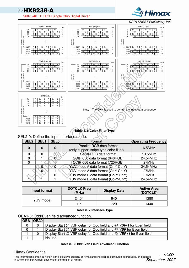
SWD2-0: Control and switch the relationship between the R, G, B data and color filter type.
-P.22- This information contained herein is the exclusive property of Himax and shell not be distributed, reproduced, or disclosed in whole or in part without prior written permission of Himax.
Himax Confidential
September, 2007
HX8238-A 960x 240 TFT LCD Single Chip Digital Driver
DATA SHEET Preliminary V03
R G B R G BRG B RG B R GB RG B
R G B R G B
RG B RG B
R G B R G BR GB RG B
……
SWD[2:0]=000 SWD [2:0]= 001
RG B RG B
SWD [2:0]=01X
SWD[2:0]=100
R GB RG B
SWD [2:0]= 101
RG B RG B
R G B R G B
R GB RG B
SWD[2:0]=110
R G B R G B
SWD[2:0]=111
R G B R G B
R G B R G B
RG B RG B
R G B R G BRG B RG B
R G B R G BRG B RG B
G1
G2
G3
G4
G240
G237
G238
G239
QXH
L
H
L
H
L
H
L
H
R GB RG B
RG B RG B
……
R GB RG BRG B RG B
R GB RG BRG B RG B
G1
G2
G3
G4
G240
G237
G238
G239
QXH
L
H
L
H
L
H
L
H
R G B R G B
R GB RG B
……
R G B R G BR GB RG B
R G B R G BR GB RG B
G1
G2
G3
G4
G240
G237
G238
G239
QXH
L
H
L
H
L
H
L
H
R G B R G BRG B RG B
……
R G B R G BRG B RG B
R G B R G BRG B RG B
G1
G2
G3
G4
G240
G237
G238
G239
QXH
L
H
L
H
L
H
L
H
R GB RG BRG B RG B
……
R GB RG BRG B RG B
R GB RG BRG B RG B
G1
G2
G3
G4
G 240
G237
G238
G239
QXH
L
H
L
H
L
H
L
H
R G B R G BR GB RG B
……
R G B R G BR GB RG B
R G B R G BR GB RG B
G1
G2
G3
G4
G240
G237
G238
G239
QXH
L
H
L
H
L
H
L
H
R G B R G B
R G B R G B
……
R G B R G B
R G B R G B
R G B R G BR G B R G B
G1
G2
G3
G4
G240
G237
G238
G239
QXH
L
L
L
L
L
L
L
L
Note:The QXH is used to control the input data sequence.
240
Lin
es
234
Lin
es
240
Lin
es
234
Lin
es
240
Lin
es
234
Lin
es
240L
ines
234L
ines
240L
ines
234L
ines
24
0Lin
es
23
4Lin
es
240
Lin
es
234
Lin
es
Table 8. 6 Color Filter Type
SEL2-0: Define the input interface mode. SEL2 SEL1 SEL0 Format Operating Frequency
0 0 0 Parallel-RGB data format
(only support stripe type color filter) 6.5MHz
0 0 1 Serial-RGB data format 19.5MHz 0 1 0 CCIR 656 data format (640RGB) 24.54MHz 0 1 1 CCIR 656 data format (720RGB) 27MHz 1 0 0 YUV mode A data format (Cr-Y-Cb-Y) 24.54MHz 1 0 1 YUV mode A data format (Cr-Y-Cb-Y) 27MHz 1 1 0 YUV mode B data format (Cb-Y-Cr-Y) 27MHz 1 1 1 YUV mode B data format (Cb-Y-Cr-Y) 24.54MHz
Input format DOTCLK Freq
(MHz) Display Data
Active Area (DOTCLK)
24.54 640 1280 YUV mode
27 720 1440
Table 8. 7 Interface Type
OEA1-0: Odd/Even field advanced function. OEA1 OEA0
0 0 Display Start @ VBP delay for Odd field and @ VBP-1 for Even field. 0 1 Display Start @ VBP delay for Odd field and @ VBP for Even field. 1 0 Display Start @ VBP delay for Odd field and @ VBP+1 for Even field. 1 1 No use
Table 8. 8 Odd/Even Field Advanced Function

-P.23- This information contained herein is the exclusive property of Himax and shell not be distributed, reproduced, or disclosed in whole or in part without prior written permission of Himax.
Himax Confidential
September, 2007
HX8238-A 960x 240 TFT LCD Single Chip Digital Driver
DATA SHEET Preliminary V03
BLT [1:0]: Set the initial power on black image insertion time. 00: 10 fields 01: 20 fields 10: 40 fields 11: 80 fields PALM: Set the input data line number in PAL mode 0: 280 lines 1: 288 lines
Function Control (R05h)
R/W R/S IB15 IB14 IB13 IB12 IB11 IB10 IB9 IB8 IB7 IB6 IB5 IB4 IB3 IB2 IB1 IB0 W 1 GHN XDK GDIS LPF DEP CKP VSP HSP DEO D I T 0 PWM 0 FB2 FB1 FB0
Figure 8. 7 Function control
FB2-0: Set PWM feedback level adjustment. 000: 0.4V 001: 0.45V 010: 0.5V 011: 0.55V 100: 0.6V 101: 0.65V 110: 0.7V 111: 0.75V
PWM: When PWM=0, PWM function is disabled. When PWM=1, PWM function is enabled.
DIT: When DIT=0, dithering function is turned off. When DIT=1, dithering function is enabled.
DEO: When DEO=0, VSYNC/HSYNC are also needed in DE mode. Under this condition, vertical back porch is defined by VBP [6:0] and the horizontal first valid data is defined by DE signal. When DEO=1, only DEN signal is needed in DE mode.
HSP: When HSP=0, HSYNC is negative polarity. When HSP=1, HSYNC is positive polarity.
VSP: When VSP=0, VSYNC is negative polarity. When VSP=1, VSYNC is positive polarity.
CKP: When CKP=0, data is latched in CLK falling edge. When CKP=1, data is latched by CLK rising edge.
DEP: When DEP=0, DEN is negative polarity active. When DEP=1, DEN is positive polarity active.
LPF: When LPF=0, the low pass filter function in YUV mode is disabled. When LPF=1, the low pass filter function is YUV mode is enabled.
GDIS: When GDIS=0, VGL has no discharge path to VSS in sleep mode. When GDIS=1, VGL will discharge to VSS in sleep mode. When CPE=0, GDIS is fixed to 0, and you can’t change it by SPI.
XDK: When XDK=0, VCIX2 is 2 stage pumping from VCI. (VCIX2=3 x VCI) When XDK=1, VCIX2 is 2 phase pumping from VCI. (VCIX2=2 x VCI)
GHN: When GHN=0, all gate outputs are forced to VGH. When GHN=1, gate driver is normal operation.

-P.24- This information contained herein is the exclusive property of Himax and shell not be distributed, reproduced, or disclosed in whole or in part without prior written permission of Himax.
Himax Confidential
September, 2007
HX8238-A 960x 240 TFT LCD Single Chip Digital Driver
DATA SHEET Preliminary V03
Contrast/Brightness Control (R0Ah) R/W R/S IB15 IB14 IB13 IB12 IB11 IB10 IB9 IB8 IB7 IB6 IB5 IB4 IB3 IB2 IB1 IB0 W 1 0 BR6 BR5 BR4 BR3 BR2 BR1 BR0 0 0 0 CON4 CON3 CON2 CON1 CON0
Figure 8. 8 Contrast/Brightness Control
CON4-0: Display Contrast level adjustment. (0.125/step) Adjust range from 00h (level =
0) to 1Fh (level = 3.875). Default value is 08h (level = 1). BR6-0: Display Brightness level adjustment. (2/step) Adjust range from 00h (level = -128)
to 7Fh (level = +126). Default value is 40h (level = 0).
Frame Cycle Control (R0Bh) R/W R/S IB15 IB14 IB13 IB12 IB11 IB10 IB9 IB8 IB7 IB6 IB5 IB4 IB3 IB2 IB1 IB0 W 1 N O 1 NO0 SDT1 SDT0 0 EQ2 EQ1 EQ0 0 0 0 0 0 0 0 0
Figure 8. 9 Frame Cycle Control
NO1-0: Sets amount of non-overlap of the gate output. NO1 NO0 Amount of non-overlap
0 0 1.5 us
0 1 3 us
1 0 4.5 us
1 1 6 us
Table 8. 9 Amount of Non-overlap
Figure 8. 10 NO Timing Diagram
SDT1-0: Set delay amount from the gate output signal falling edge to the source outputs.
SDT1 SDT0 Delay amount of the source output
0 0 1µs
0 1 3µs
1 0 5µs
1 1 7µs
Table 8. 10 Delay Amount of Source Output
EQ2-0: Sets the equalizing period. EQ2 EQ1 EQ0 EQ period
0 0 0 No EQ
0 0 1 3µs
0 1 0 4µs
0 1 1 5µs 1 0 0 6µs 1 0 1 7µs 1 1 0 8µs 1 1 1 9µs
Table 8. 11 EQ Period

-P.25- This information contained herein is the exclusive property of Himax and shell not be distributed, reproduced, or disclosed in whole or in part without prior written permission of Himax.
Himax Confidential
September, 2007
HX8238-A 960x 240 TFT LCD Single Chip Digital Driver
DATA SHEET Preliminary V03
1 Line period 1 Line period
Gn
Sn
EQ
Delay amount of
The source output
Equalizing
Period
Figure 8. 11 EQ Timing Diagram
Power Control 2 (R0Dh) R/W R/S IB15 IB14 IB13 IB12 IB11 IB10 IB9 IB8 IB7 IB6 IB5 IB4 IB3 IB2 IB1 IB0 W 1 0 VRC2 VRC1 VRC0 0 0 VDS1 VDS0 0 0 VRH5 VRH4 VRH3 VRH2 VRH1 VRH0
Figure 8. 12 Power Control 2
VRC [2:0]: set the VCIX2 charge pump voltage clamp. VRC [2:0]=000, 5.1V
VRC [2:0]=001, 5.3V VRC [2:0]=010, 5.5V
VRC [2:0]=011, 5.7V VRC [2:0]=100, 5.9V
VRC [2:0]=101, reserved VRC [2:0]=110, reserved VRC [2:0]=111, reserved
VDS [1:0]: set the VDD regulator voltage if pin “REGVDD” is set to VDDIO. VDS [1:0]=00, 1.8V VDS [1:0]=01, 2.0V VDS [1:0]=10, 2.2V
VDS [1:0]=11, 2.5V VRH5-0: Set amplitude magnification of VLCD63. These bits amplify the VLCD63
voltage 2.464 to 4.456 times the Vref voltage set by VRH5-0.

-P.26- This information contained herein is the exclusive property of Himax and shell not be distributed, reproduced, or disclosed in whole or in part without prior written permission of Himax.
Himax Confidential
September, 2007
HX8238-A 960x 240 TFT LCD Single Chip Digital Driver
DATA SHEET Preliminary V03
VRH5 VRH4 VRH3 VRH2 VRH1 VRH0 VLCD63Voltage VRH5 VRH4 VRH3 VRH2 VRH1 VRH0 VLCD63Voltage
0 0 0 0 0 0 Vref x 2.456 1 0 0 0 0 0 Vref x 3.480
0 0 0 0 0 1 Vref x 2.488 1 0 0 0 0 1 Vref x 3.512
0 0 0 0 1 0 Vref x 2.520 1 0 0 0 1 0 Vref x 3.544
0 0 0 0 1 1 Vref x 2.552 1 0 0 0 1 1 Vref x 3.576
0 0 0 1 0 0 Vref x 2.584 1 0 0 1 0 0 Vref x 3.608
0 0 0 1 0 1 Vref x 2.616 1 0 0 1 0 1 Vref x 3.640
0 0 0 1 1 0 Vref x 2.648 1 0 0 1 1 0 Vref x 3.672
0 0 0 1 1 1 Vref x 2.680 1 0 0 1 1 1 Vref x 3.704
0 0 1 0 0 0 Vref x 2.712 1 0 1 0 0 0 Vref x 3.736
0 0 1 0 0 1 Vref x 2.744 1 0 1 0 0 1 Vref x 3.768
0 0 1 0 1 0 Vref x 2.776 1 0 1 0 1 0 Vref x 3.800
0 0 1 0 1 1 Vref x 2.808 1 0 1 0 1 1 Vref x 3.832
0 0 1 1 0 0 Vref x 2.840 1 0 1 1 0 0 Vref x 3.864
0 0 1 1 0 1 Vref x 2.872 1 0 1 1 0 1 Vref x 3.896
0 0 1 1 1 0 Vref x 2.904 1 0 1 1 1 0 Vref x 3.928
0 0 1 1 1 1 Vref x 2.936 1 0 1 1 1 1 Vref x 3.960
0 1 0 0 0 0 Vref x 2.968 1 1 0 0 0 0 Vref x 3.992
0 1 0 0 0 1 Vref x 3.000 1 1 0 0 0 1 Vref x 4.024
0 1 0 0 1 0 Vref x 3.032 1 1 0 0 1 0 Vref x 4.056
0 1 0 0 1 1 Vref x 3.064 1 1 0 0 1 1 Vref x 4.088
0 1 0 1 0 0 Vref x 3.096 1 1 0 1 0 0 Vref x 4.120
0 1 0 1 0 1 Vref x 3.128 1 1 0 1 0 1 Vref x 4.152
0 1 0 1 1 0 Vref x 3.160 1 1 0 1 1 0 Vref x 4.184
0 1 0 1 1 1 Vref x 3.192 1 1 0 1 1 1 Vref x 4.216
0 1 1 0 0 0 Vref x 3.224 1 1 1 0 0 0 Vref x 4.248
0 1 1 0 0 1 Vref x 3.256 1 1 1 0 0 1 Vref x 4.280
0 1 1 0 1 0 Vref x 3.288 1 1 1 0 1 0 Vref x 4.312
0 1 1 0 1 1 Vref x 3.320 1 1 1 0 1 1 Vref x 4.344
0 1 1 1 0 0 Vref x 3.352 1 1 1 1 0 0 Vref x 4.376
0 1 1 1 0 1 Vref x 3.384 1 1 1 1 0 1 Vref x 4.408
0 1 1 1 1 0 Vref x 3.416 1 1 1 1 1 0 Vref x 4.440
0 1 1 1 1 1 Vref x 3.448 1 1 1 1 1 1 Vref x 4.472
Note: Vref is the internal reference voltage equals to 1.25V.
Table 8. 12 VLCD63 Voltage
-P.27- This information contained herein is the exclusive property of Himax and shell not be distributed, reproduced, or disclosed in whole or in part without prior written permission of Himax.
Himax Confidential
September, 2007
HX8238-A 960x 240 TFT LCD Single Chip Digital Driver
DATA SHEET Preliminary V03
Power Control 3 (R0Eh) R/W R/S IB15 IB14 IB13 IB12 IB11 IB10 IB9 IB8 IB7 IB6 IB5 IB4 IB3 IB2 IB1 IB0 W 1 0 0 1 VDV6 VDV5 VDV4 VDV3 VDV2 VDV1 VDV0 0 0 0 0 0 0
Figure 8. 13 Power Control 3
VDV6-0: Set the alternating amplitudes of VCOM at the VCOM alternating drive. These
bits amplify VCOM amplitude 0.6 to 1.2525 times the VLCD63 voltage. External voltage at VCOMR is referenced when VDV = “01111xx”.
VDV6 VDV5 VDV4 VDV3 VDV2 VDV1 VDV0 VCOM Amplitude
0 0 0 0 0 0 0 VLCD63 x 0.6000 0 0 0 0 0 0 1 VLCD63 x 0.6075 0 0 0 0 0 1 0 VLCD63 x 0.6150
0 0 0 0 0 1 1 VLCD63 x 0.6225 0 0 0 0 1 0 0 VLCD63 x 0.6300
: : :
: Step = 0.0075
:
0 1 1 1 0 1 0 VLCD63 x 1.0350 0 1 1 1 0 1 1 VLCD63 x 1.0425
0 1 1 1 1 * * Reference from external voltage
(VCOMR) 1 0 0 0 0 0 0 VLCD63 x 1.0500
1 0 0 0 0 0 1 VLCD63 x 1.0575 : : :
: Step = 0.0075
: 1 0 1 1 0 1 0 VLCD63 x 1.2450 1 0 1 1 0 1 1 VLCD63 x 1.2525
1 0 1 1 1 * * Reserved 1 1 * * * * * Reserved
Table 8. 13 VCOM Amplitude
Gate Scan Position (R0Fh)
R/W R/S IB15 IB14 IB13 IB12 IB11 IB10 IB9 IB8 IB7 IB6 IB5 IB4 IB3 IB2 IB1 IB0 W 1 0 0 0 0 0 0 0 0 SCN7 SCN6 SCN5 SCN4 SCN3 SCN2 SCN1 SCN0
Figure 8. 14 Gate Scan Position
SCN8-0: Set the scanning starting position of the gate driver.
HIMAX
TECHNOLOGIES
奇景光電奇景光電奇景光電奇景光電
TECHNOLOGIES
奇景光電奇景光電奇景光電奇景光電
HIMAX
G0
G239
1st line of
data
SCN7-0
= 00000000
G0
G239
G30 1st
line of
data
SCN7-0
= 00011110
Figure 8. 15 Gate scan display position

-P.28- This information contained herein is the exclusive property of Himax and shell not be distributed, reproduced, or disclosed in whole or in part without prior written permission of Himax.
Himax Confidential
September, 2007
HX8238-A 960x 240 TFT LCD Single Chip Digital Driver
DATA SHEET Preliminary V03
Horizontal Porch (R16h) R/W R/S IB15 IB14 IB13 IB12 IB11 IB10 IB9 IB8 IB7 IB6 IB5 IB4 IB3 IB2 IB1 IB0 W 1 XLIM8 X L IM7 XLIM6 XLIM5 XLIM4 XLIM3 XLIM2 XLIM1 XLIM0 0 0 0 0 0 0 0
Figure 8. 16 Horizontal Porch
XLIM8-0: Set the number of valid pixel per line. XLIM8 XLIM7 XLIM6 XLIM5 XLIM4 XLIM3 XLIM2 XLIM1 XLIM0 No. of pixel per line
0 0 0 0 0 0 0 0 0 1 0 0 0 0 0 0 0 0 1 2
0 0 0 0 0 0 0 1 0 3 : : :
: Step = 1
:
1 0 0 1 1 1 1 1 0 319 1 0 0 1 1 1 1 1 1 320
1 0 1 ∗ ∗ ∗ ∗ ∗ ∗ Reserved
1 1 ∗ ∗ ∗ ∗ ∗ ∗ ∗ Reserved
Table 8. 14 No. of Pixel Per Line

-P.29- This information contained herein is the exclusive property of Himax and shell not be distributed, reproduced, or disclosed in whole or in part without prior written permission of Himax.
Himax Confidential
September, 2007
HX8238-A 960x 240 TFT LCD Single Chip Digital Driver
DATA SHEET Preliminary V03
Vertical Porch (R17h) R/W R/S IB15 IB14 IB13 IB12 IB11 IB10 IB9 IB8 IB7 IB6 IB5 IB4 IB3 IB2 IB1 IB0 W 1 STH1 STH0 HBP6 HBP5 HBP4 HBP3 HBP2 HBP1 HBP0 VBP6 VBP5 VBP4 VBP3 VBP2 VBP1 VBP0
Figure 8. 17 Vertical Porch
HBP6-0: Set the delay period from falling edge of HSYNC signal to first valid data. The pixel data exceed the range set by XLIM8-0 and before the first valid data will be treated as dummy data. The setting is only effective in SYNC mode timing.
HBP6 HBP5 HBP4 HBP3 HBP2 HBP1 HBP0 No. of Clock Cycle
0 0 0 0 0 0 0 Can’t set 0 0 0 0 0 0 1 Can’t set 0 0 0 0 0 1 0 Can’t set
0 0 0 0 0 1 1 Can’t set 0 0 0 0 1 0 0 Can’t set
0 0 0 0 1 0 1 Can’t set 0 0 0 0 1 1 0 Can’t set 0 0 0 0 1 1 1 Can’t set 0 0 0 1 0 0 0 Can’t set 0 0 0 1 0 0 1 9
:
Step = 1 :
1 1 1 1 1 1 0 126 1 1 1 1 1 1 1 127
Table 8. 15 No. of Clock Cycle of Clock
Cycle time of HSYNC
Set by HBP6-0 Set by XLIM8-0
HSYNC
Pixel Data
DOTCLK
Default 320 pixels per line
10 clock cycles of DOTCLKHBP6-0 = 00001000
D0 D1 D2 D317 D318 D319Dummy Dummy
Figure 8. 18 No. of Clock Cycle of Clock

-P.30- This information contained herein is the exclusive property of Himax and shell not be distributed, reproduced, or disclosed in whole or in part without prior written permission of Himax.
Himax Confidential
September, 2007
HX8238-A 960x 240 TFT LCD Single Chip Digital Driver
DATA SHEET Preliminary V03
STH1-0: Adjust the first valid data by dot clock. This setting is not valid in parallel RGB input interface. STH = 00: +0 dot clock STH = 01: +1 dot clock STH = 10: +2 dot clock STH = 11: +3 dot clock
VBP6-0: Set the delay period from falling edge of VSYNC to first valid line. The line data
within this delay period will be treated as dummy line. The setting is only effective in SYNC mode timing.
VBP6 VBP5 VBP4 VBP3 VBP2 VBP1 VBP0 No. of clock cycle of HSYNC
0 0 0 0 0 0 0 Can’t set 0 0 0 0 0 0 1 Can’t set
0 0 0 0 0 1 0 2 0 0 0 0 0 1 1 3
0 0 0 0 1 0 0 4 :
Step = 1 :
1 1 1 1 1 0 0 124 1 1 1 1 1 0 1 125
1 1 1 1 1 1 0 126
1 1 1 1 1 1 1 127
Table 8. 16 No. of Clock Cycle of HSYNC
Cycle time of VSYNC
Set by VBP6-0
VSYNC
HSYNC
Dummy Lines Dummy Lines1st Line Last Line
Figure 8. 19 No. of Clock Cycle of HSYNC
Power Control 4 (R1Eh)
R/W R/S IB15 IB14 IB13 IB12 IB11 IB10 IB9 IB8 IB7 IB6 IB5 IB4 IB3 IB2 IB1 IB0 W 1 0 0 0 0 0 0 0 0 nOTP VCM6 VCM5 VCM4 VCM3 VCM2 VCM1 VCM0
Figure 8. 20 Power Control 4
nOTP: nOTP equals to “0” after power on reset and VCOMH voltage equals to
programmed OTP value. When nOTP set to “1”, setting of VCM6-0 becomes valid and voltage of VCOMH can be adjusted.

-P.31- This information contained herein is the exclusive property of Himax and shell not be distributed, reproduced, or disclosed in whole or in part without prior written permission of Himax.
Himax Confidential
September, 2007
HX8238-A 960x 240 TFT LCD Single Chip Digital Driver
DATA SHEET Preliminary V03
VCM6-0: Set the VCOMH voltage if nOTP = “1”. These bits amplify the VCOMH voltage 0.36 to 0.995 times the VLCD63 voltage.
VCM6 VCM5 VCM4 VCM3 VCM2 VCM1 VCM0 VCOMH
0 0 0 0 0 0 0 VLCD63 x 0.360 0 0 0 0 0 0 1 VLCD63 x 0.365 0 0 0 0 0 1 0 VLCD63 x 0.370 0 0 0 0 0 1 1 VLCD63 x 0.375 0 0 0 0 1 0 0 VLCD63 x 0.380
: : :
: :
: Step = 0.005
:
1 1 1 1 1 0 0 VLCD63 x 0.980 1 1 1 1 1 0 1 VLCD63 x 0.985 1 1 1 1 1 1 0 VLCD63 x 0.990 1 1 1 1 1 1 1 VLCD63 x 0.995
Note: 2V < VCOMH < VLCD63
Table 8. 17 VCOMH
Gamma Control 1 (R30h to R37h) R/W R/S IB15 IB14 IB13 IB12 IB11 IB10 IB9 IB8 IB7 IB6 IB5 IB4 IB3 IB2 IB1 IB0 W 1 0 0 0 0 0 PKP12 PKP11 PKP10 0 0 0 0 0 PKP02 PKP01 PKP00
W 1 0 0 0 0 0 PKP32 PKP31 PKP30 0 0 0 0 0 PKP22 PKP21 PKP20
W 1 0 0 0 0 0 PKP52 PKP51 PKP50 0 0 0 0 0 PKP42 PKP41 PKP40
W 1 0 0 0 0 0 PRP12 PRP11 PRP10 0 0 0 0 0 PRP02 PRP01 PRP00
W 1 0 0 0 0 0 PKN12 PKN11 PKN10 0 0 0 0 0 PKN02 PKN01 PKN00
W 1 0 0 0 0 0 PKN32 PKN31 PKN30 0 0 0 0 0 PKN22 PKN21 PKN20
W 1 0 0 0 0 0 PKN52 PKN51 PKN50 0 0 0 0 0 PKN42 PKN41 PKN40
W 1 0 0 0 0 0 PRN12 PRN11 PRN10 0 0 0 0 0 PRN02 PRN02 PRN00
Figure 8. 21 Gamma Control 1
PKP52–00: Gamma micro adjustment registers for the positive polarity output. PRP12-00: Gradient adjustment registers for the positive polarity output. PKN52-00: Gamma micro adjustment registers for the negative polarity output. PRN12-00: Gradient adjustment registers for the negative polarity output.
Gamma Control 2 (R3Ah to R3Bh)
R/W R/S IB15 IB14 IB13 IB12 IB11 IB10 IB9 IB8 IB7 IB6 IB5 IB4 IB3 IB2 IB1 IB0 W 1 0 0 0 VRP14 VRP13 VRP12 VRP11 VRP10 0 0 0 0 VRP03 VRP02 VRP01 VRP00
W 1 0 0 0 VRN14 VRN13 VRN12 VRN11 VRN10 0 0 0 0 VRN03 VRN02 VRN01 VRN00
Figure 8. 22 Gamma Control 2
VRP14-00: Adjustment registers for amplification adjustment of the positive polarity output.
VRN14-00: Adjustment registers for the amplification adjustment of the negative polarity output.
(Refer to Gamma Adjustment Function for details)
-P.32- This information contained herein is the exclusive property of Himax and shell not be distributed, reproduced, or disclosed in whole or in part without prior written permission of Himax.
Himax Confidential
September, 2007
HX8238-A 960x 240 TFT LCD Single Chip Digital Driver
DATA SHEET Preliminary V03
9. OTP Programming OTP Write Sequence
Step Operation
1 Power up the module. Set nOTP=1 and find out the appropriate value of VCM[6:0] and power off the system
2 Power up the system with VDD=VDDIO=2.5V. If REGVDD=1, set R0Dh=16’h0324.
3 Set appropriate values found from step 1 to register of VCOM (R1Eh)
4 Set R06h=16’h2820 to stop VGH/VGL pumping. Wait 0.5s.
5 Set R60h=16’h8000
6 Set R60h=16’hC000
7 Connect 7.3V to VGH and 0V to VGL (Note1)
8 Set R60h=16’hC200
9 Set R60h=16’hC280
10 Wait 200us for completing this program
11 Set R60h=16’hC200
12 Remove 7.3V from VGH and 0V from VGL
13 Set R60h=16’h8200
14 Set R60h=16’h0200
15 Set R60h=16’h0040
16 Set R60h=16’h0000
Note: VGH is connected to 7.1~7.4
Table 9. 1 OTP Programming Sequence
You can use above programming sequence to set VCM [6:0] value to OTP cell once. Before you program the OTP cell, the default VCM [6:0] =1010010 in OTP of Part NO. which is HX8238-A00BPDXXX, the default VCM [6:0] =1011111 in OTP of Part NO. which is HX8238-A02BPDXXX. If you want to check if the OTP cell is till available for programming, you can read the status from R61h shown below.
R/W R/S IB15 IB14 IB13 IB12 IB11 IB10 IB9 IB8 IB7 IB6 IB5 IB4 IB3 IB2 IB1 IB0
R 1 0 0 0 0 0 0 0 0 I ND VCM6 VCM5 VCM4 VCM3 VCM2 VCM1 VCM0
Figure 9. 1 OTP Read Table
You can check the IND bit to see if the VCM [6:0] is still programmable or not. If IND=0, you can program new VCM [6:0] value to OTP. If IND=1, it means that the OTP cell have already programmed and you can’t program it any more. IB6~IB0 indicate the currently effective VCM [6:0] setting in OTP cell.
OTP Programming circuitry
HX8238-A
V GH
V GL +
-
GND
GND
Apply voltage at Step (7)
Note: C = 1uF
(built -in on the module)
7.3 V
C
+
GND
-
Figure 9. 2 OTP Programming Circuitry

-P.33- This information contained herein is the exclusive property of Himax and shell not be distributed, reproduced, or disclosed in whole or in part without prior written permission of Himax.
Himax Confidential
September, 2007
HX8238-A 960x 240 TFT LCD Single Chip Digital Driver
DATA SHEET Preliminary V03
10. Gamma Adjustment Function
The HX8238-A incorporates gamma adjustment function for the 262K-color display. Gamma adjustment is implemented by deciding the 8-grayscale levels with angle adjustment and micro adjustment register. Also, angle adjustment and micro adjustment is fixed for each of the internal positive and negative polarity. Set up by the liquid crystal panel’s specification.
LCD
R5 R4 R3 R2 R1 R0 G5 G4 G3 G2 G1 G0 B5 B4 B3 B2 B1 B0
RGB Interface
64 grayscale Control<R>
LCD Driver
64 grayscale Control<R>
LCD Driver
64 grayscale Control<R>
LCD Driver
R G B
Grayscale amplifier
PKP02 PKP01 PKP00
PKP12 PKP11 PKP10
PKP22 PKP21 PKP20
PKP32 PKP31 PKP30
PKP42 PKP41 PKP40
PKP52 PKP51 PKP50
PRP02 PRP01 PRP00
PRP12 PRP11 PRP10
VRP02 VRP01 VRP00
VRP12 VRP11 VRP10 VRP13
VRP03
VRP14
Positive
polarity
register
PKN02 PKN01 PKN00
PKN12 PKN11 PKN10
PKN22 PKN21 PKN20
PKN32 PKN31 PKN30
PKN42 PKN41 PKN40
PKN52 PKN51 PKN50
PRN02 PRN01 PRN00
PRN12 PRN11 PRN10
VRN02 VRN01 VRN00
VRN12 VRN11 VRN10 VRN13
VRN03
VRN14
Negative
polarity
register
8-LEVELS 64-LEVELS
V0
V63
Display Data
6-bits 6-bits 6-bits
Figure 10. 1 Grayscale Control Block

-P.34- This information contained herein is the exclusive property of Himax and shell not be distributed, reproduced, or disclosed in whole or in part without prior written permission of Himax.
Himax Confidential
September, 2007
HX8238-A 960x 240 TFT LCD Single Chip Digital Driver
DATA SHEET Preliminary V03
10.1 Structure of Grayscale Amplifier
Below figure indicates the structure of the grayscale amplifier. It determines 8 levels (VIN0-VIN7) by the gradient adjuster and the micro adjustment register. Also, dividing these levels with ladder resistors generates V0 to V63.
Gradient Adjustment register
PRP0 PRP1
Micro adjustment register
PKP0 PKP1 PKP2 PKP3 PKP4 PKP5
Amplitude Adjustment register
VRP0 VRP1 VLCD63
La
dde
r re
sis
tor
Gra
ysca
le A
mp
lifie
r
8 to 1
selector
8 to 1
selector
8 to 1
selector
8 to 1
selector
8 to 1
selector
8 to 1
selector
EXVR
* Individual ladder resistors are used for positive and negative polarity.
3 3 3 3 3 3 3 3 4 5
VINP0
VINP1
VINP2
VINP3
VINP4
VINP5
VINP6
VINP7
V0
V1
:
V7
V8
:
V19
V20
:
V42
V43
:
V54
V55
:
V61
V62
:
V63
Figure 10. 2 Grayscale Amplifier

-P.35- This information contained herein is the exclusive property of Himax and shell not be distributed, reproduced, or disclosed in whole or in part without prior written permission of Himax.
Himax Confidential
September, 2007
HX8238-A 960x 240 TFT LCD Single Chip Digital Driver
DATA SHEET Preliminary V03
Figure 10. 3 Resistor Ladder for Gamma Voltages Generation
VLCD63 VRP0 [3:0]
VINP0
PK P0 [
2 :0]
KVP0
KVP 1
KVP 2
KVP 4
KVP 5
KVP 7
KVP 8
KVP 3
KVP 6
8 to 1
selector
VINP1
R P 0
R P 1
R P 2
R P 3
R P 4
R P 5
R P 6
R P 7
4 R x7
5 R
0 to 30R
VRP0
P RP0[ 2 :0] PK P 1 [ 2 :0]
KVP 9
KVP 10
KVP 12
KVP 13
KVP 15
KVP 16
KVP 11
KVP 14
8 to 1
selector
VINP2
R P 8
R P 9
R P 10
R P 11
R P 12
R P 13
R P 14
1R x7
0 to 28R
VRHP
PK P 2 [ 2 :0]
KVP 17
KVP 18
KVP 20
KVP 21
KVP 23
KVP 24
KVP 19
KVP 22
8 to 1
selector
VINP3
R P 16
R P 17
R P 18
R P 19
R P 20
R P 21
R P 22
1R x7
PK P 3 [ 2 :0]
KVP 25
KVP 26
KVP 28
KVP 29
KVP 31
KVP 32
KVP 27
KVP 30
8 to 1
selector
VINP4
R P 24
R P 25
R P 26
R P 27
R P 28
R P 29
R P 30
1R x7
PK P 4 [ 2 :0]
KVP 33
KVP 34
KVP 36
KVP 37
KVP 39
KVP 40
KVP 35
KVP 38
8 to 1
sele ctor
VINP5
R P 32
R P 33
R P 34
R P 35
R P 36
R P 37
R P 38
1R x7
R P 15
R P 23
R P 31
PK P 5 [ 2 :0]
KVP 41
KVP 42
KVP 44
KVP 45
KVP 47
KVP 48
KVP 43
KVP 46
8 to 1
selector
VINP6
R P 39
R P 40
R P 41
R P 42
R P 43
R P 44
R P 45
4 R x7
PRP 1 [ 2 :0]
0 to 28R
VRLP
0 to 31R
VRP1
VINP7
V RP 1 [ 4 :0]
EXVR
VRN 0[ 3:0]
VINN0
PKN 0[ 2 :0]
KVN 0
KVN1
KVN2
KVN4
KVN5
KVN7
KVN8
KVN3
KVN6
8 to 1
selector
VINN1
RN0
RN1
RN2
RN3
RN4
RN5
RN6
RN7
4 R x7
5R
0 to 30R
VRN0
PRN 0[ 2 :0] PKN1 [ 2 :0]
KVN 9
KVN 10
KVN 12
KVN 13
KVN 16
KVN 11
KVN 14
8 to 1
selector
VINN2
RN8
RN9
RN10
RN11
RN12
RN13
RN14
1R
0 to 28R
VRH N
PKN2 [ 2 :0]
KVN 17
KVN 18
KVN 20
KVN 21
KVN 23
KVN 24
KVN 19
KVN 22
8 to 1
selector
VINN3
RN16
RN17
RN18
RN19
RN20
RN21
RN22
1R x7
PKN3 [ 2 :0]
KVN 25
KVN 26
KVN 28
KVN 29
KVN 31
KVN 32
KVN 27
KVN 30
8 to 1
selector
VINN4
RN24
RN25
RN26
RN27
RN28
RN29
RN30
1R x7
PKN4 [ 2 :0]
KVN 33
KVN 34
KVN 36
KVN 37
KVN 39
KVN 40
KVN 35
KVN 38
8 to 1
selector
VINN5
RN32
RN33
RN34
RN35
RN36
RN37
RN38
1R x7
RN 15
RN23
RN3 1
PKN5 [ 2 :0]
KVN 41
KVN 42
KVN 44
KVN 45
KVN 47
KVN 48
KVN 43
KVN 46
8 to 1
selector
VINN6
RN39
RN40
RN41
RN42
RN43
RN44
RN45
4 R x7
PRN 1 [ 2 :0]
0 to 28R
VRL N
0 to 31R
VRN1 8R
VINN7
VRN 1 [ 4 :0]
R P 47
R N47
R N46
5 R
16 R
5 R
5 R
R P 46
5R
16 R
5R
5R
8R

-P.36- This information contained herein is the exclusive property of Himax and shell not be distributed, reproduced, or disclosed in whole or in part without prior written permission of Himax.
Himax Confidential
September, 2007
HX8238-A 960x 240 TFT LCD Single Chip Digital Driver
DATA SHEET Preliminary V03
10.2 Gamma Adjustment Register
This block is the register to set up the grayscale voltage adjusting to the gamma specification of the LCD panel. This register can independent set up to positive/negative polarities and there are three types of register groups to adjust gradient, amplitude, and micro-adjustment on number of the grayscale, characteristics of the grayscale voltage. (Using the same setting for Reference-value and R.G.B.) Following graphics indicates the operation of each adjusting register.
Figure 10. 4 Gamma Adjustment Function
10.2.1 Gradient Adjusting Register
The gradient-adjusting resistor is to adjust around middle gradient, specification of the grayscale number and the grayscale voltage without changing the dynamic range. To accomplish the adjustment, it controls the variable resistors in the middle of the ladder resistor by registers (PRP (N) 0 / PRP (N) 1) for the grayscale voltage generator. Also, there is an independent resistor on the positive/negative polarities in order for corresponding to asymmetry drive.
10.2.2 Amplitude Adjusting Register
The amplitude-adjusting resistor is to adjust amplitude of the grayscale voltage. To accomplish the adjustment, it controls the variable resistors in the boundary of the ladder resistor by registers (VRP (N) 0 / VRP (N) 1) for the grayscale voltage generator. Also, there is an independent resistor on the positive/negative polarities as well as the gradient-adjusting resistor.
10.2.3 Micro Adjusting Register
The micro-adjusting register is to make subtle adjustment of the grayscale voltage level. To accomplish the adjustment, it controls each reference voltage level by the 8 to 1 selector towards the 8-level reference voltage generated from the ladder resistor. Also, there is an independent resistor on the positive/negative polarities as well as other adjusting resistors.

-P.37- This information contained herein is the exclusive property of Himax and shell not be distributed, reproduced, or disclosed in whole or in part without prior written permission of Himax.
Himax Confidential
September, 2007
HX8238-A 960x 240 TFT LCD Single Chip Digital Driver
DATA SHEET Preliminary V03
10.3 Ladder Resistor / 8 to 1 Selector
This block outputs the reference voltage of the grayscale voltage. There are two ladder resistors including the variable resistor and the 8 to 1 selector selecting voltage generated by the ladder resistor. The gamma registers control the variable resistors and 8 to 1 selector resistors. Also, there has pin (EXVR) that can be connected to VSS or an external variable resistor for compensating the dispersion of length between one panel to another.
Variable Resistor
There are 3 types of the variable resistors that are for the gradient and amplitude adjustment. The resistance is set by the resistor (PRP (N) 0 / PRP (N) 1) and (VRP (N) 0 / VRP (N) 1) as below.
PRP(N)[0:1] Resistance VRP(N)0 Resistance VRP(N)1 Resistance
000 0R 0000 0R 00000 0R 001 4R 0001 2R 00001 1R
010 8R 0010 4R 00010 2R
011 12R
100 16R
101 20R
: Step = 2R
:
: Step = 1R
:
110 24R 1110 28R 11110 30R 111 28R 1111 30R 11111 31R
Table 10. 1 PRP (N) Table 10. 2 VRP (N) 0 Table 10. 3 VRP (N) 1
8 to 1 Selector
In the 8 to 1 selector, a reference voltage VIN can be selected from the levels which are generated by the ladder resistors. There are six types of reference voltage (VIN1 to VIN6) and totally 48 divided voltages can be selected in one ladder resistor. Following figure explains the relationship between the micro adjusting register and the selecting voltage.
Positive polarity Negative polarity
Selected voltage Selected voltage Register PKP[2:0] VINP1 VINP2 VINP3 VINP4 VINP5 VINP6
Register PKN[2:0] VINN1 VINN2 VINN3 VINN4 VINN5 VINN6
000 KVP1 KVP9 KVP17 KVP25 KVP33 KVP41 000 KVN1 KVN9 KVN17 KVN25 KVN33 KVN41
001 KVP2 KVP10 KVP18 KVP26 KVP34 KVP42 001 KVN2 KVN10 KVN18 KVN26 KVN34 KVN42
010 KVP3 KVP11 KVP19 KVP27 KVP35 KVP43 010 KVN3 KVN11 KVN19 KVN27 KVN35 KVN43
011 KVP4 KVP12 KVP20 KVP28 KVP36 KVP44 011 KVN4 KVN12 KVN20 KVN28 KVN36 KVN44
100 KVP5 KVP13 KVP21 KVP29 KVP37 KVP45 100 KVN5 KVN13 KVN21 KVN29 KVN37 KVN45
101 KVP6 KVP14 KVP22 KVP30 KVP38 KVP46 101 KVN6 KVN14 KVN22 KVN30 KVN38 KVN46
110 KVP7 KVP15 KVP23 KVP31 KVP39 KVP47 110 KVN7 KVN15 KVN23 KVN31 KVN39 KVN47
111 KVP8 KVP16 KVP24 KVP32 KVP40 KVP48 111 KVN8 KVN16 KVN24 KVN32 KVN40 KVN48
Table 10. 4 PKP and PKN

-P.38- This information contained herein is the exclusive property of Himax and shell not be distributed, reproduced, or disclosed in whole or in part without prior written permission of Himax.
Himax Confidential
September, 2007
HX8238-A 960x 240 TFT LCD Single Chip Digital Driver
DATA SHEET Preliminary V03
Grayscale voltage
Positive Polarity Negative Polarity
V0 VINP0 VINN7 V1 VINP1 VINN6
V2 V8+(V1-V8)*(2241/2703) V1+(V8-V1)*(462/2703)
V3 V8+(V1-V8)*(1671/2703) V1+(V8-V1)*(1032/2703)
V4 V8+(V1-V8)*(1209/2703) V1+(V8-V1)*(1494/2703) V5 V8+(V1-V8)*(849/2703) V1+(V8-V1)*(1854/2703)
V6 V8+(V1-V8)*(567/2703) V1+(V8-V1)*(2136/2703)
V7 V8+(V1-V8)*(294/2703) V1+(V8-V1)*(2409/2703)
V8 VINP2 VINN5
V9 V20+(V8-V20)*(1533/1767) V8+(V20-V8)*(234/1767)
V10 V20+(V8-V20)*(1356/1767) V8+(V20-V8)*(411/1767) V11 V20+(V8-V20)*(1188/1767) V8+(V20-V8)*(579/1767)
V12 V20+(V8-V20)*(993/1767) V8+(V20-V8)*(774/1767)
V13 V20+(V8-V20)*(843/1767) V8+(V20-V8)*(924/1767)
V14 V20+(V8-V20)*(693/1767) V8+(V20-V8)*(1074/1767)
V15 V20+(V8-V20)*(543/1767) V8+(V20-V8)*(1224/1767)
V16 V20+(V8-V20)*(441/1767) V8+(V20-V8)*(1326/1767) V17 V20+(V8-V20)*(336/1767) V8+(V20-V8)*(1431/1767)
V18 V20+(V8-V20)*(213/1767) V8+(V20-V8)*(1554/1767)
V19 V20+(V8-V20)*(81/1767) V8+(V20-V8)*(1686/1767)
V20 VINP3 VINN4
V21 V43+(V20-V43)*(1887/1965) V20+(V43-V20)*(78/1965)
V22 V43+(V20-V43)*(1779/1965) V20+(V43-V20)*(186/1965) V23 V43+(V20-V43)*(1653/1965) V20+(V43-V20)*(312/1965)
V24 V43+(V20-V43)*(1536/1965) V20+(V43-V20)*(429/1965)
V25 V43+(V20-V43)*(1437/1965) V20+(V43-V20)*(528/1965)
V26 V43+(V20-V43)*(1362/1965) V20+(V43-V20)*(603/1965)
V27 V43+(V20-V43)*(1278/1965) V20+(V43-V20)*(687/1965) V28 V43+(V20-V43)*(1191/1965) V20+(V43-V20)*(774/1965)
V29 V43+(V20-V43)*(1098/1965) V20+(V43-V20)*(867/1965)
V30 V43+(V20-V43)*(1008/1965) V20+(V43-V20)*(957/1965)
V31 V43+(V20-V43)*(927/1965) V20+(V43-V20)*(1038/1965)
V32 V43+(V20-V43)*(843/1965) V20+(V43-V20)*(1122/1965)
V33 V43+(V20-V43)*(750/1965) V20+(V43-V20)*(1215/1965) V34 V43+(V20-V43)*(678/1965) V20+(V43-V20)*(1287/1965)
V35 V43+(V20-V43)*(612/1965) V20+(V43-V20)*(1353/1965)
V36 V43+(V20-V43)*(528/1965) V20+(V43-V20)*(1437/1965)
V37 V43+(V20-V43)*(450/1965) V20+(V43-V20)*(1515/1965)
V38 V43+(V20-V43)*(375/1965) V20+(V43-V20)*(1590/1965)
V39 V43+(V20-V43)*(303/1965) V20+(V43-V20)*(1662/1965) V40 V43+(V20-V43)*(222/1965) V20+(V43-V20)*(1743/1965)
V41 V43+(V20-V43)*(147/1965) V20+(V43-V20)*(1818/1965)
V42 V43+(V20-V43)*(87/1965) V20+(V43-V20)*(1878/1965)
V43 VINP4 VINN3
V44 V55+(V43-V55)*(936/1014) V43+(V55-V43)*(78/1014)
V45 V55+(V43-V55)*(867/1014) V43+(V55-V43)*(147/1014) V46 V55+(V43-V55)*(792/1014) V43+(V55-V43)*(222/1014)
V47 V55+(V43-V55)*(723/1014) V43+(V55-V43)*(291/1014)
V48 V55+(V43-V55)*(648/1014) V43+(V55-V43)*(366/1014)
V49 V55+(V43-V55)*(561/1014) V43+(V55-V43)*(453/1014)
V50 V55+(V43-V55)*(465/1014) V43+(V55-V43)*(549/1014) V51 V55+(V43-V55)*(387/1014) V43+(V55-V43)*(627/1014)
V52 V55+(V43-V55)*(291/1014) V43+(V55-V43)*(723/1014)
V53 V55+(V43-V55)*(201/1014) V43+(V55-V43)*(813/1014)
V54 V55+(V43-V55)*(111/1014) V43+(V55-V43)*(903/1014)
V55 VINP5 VINN2
V56 V62+(V55-V62)*(1218/1317) V55+(V62-V55)*(99/1317) V57 V62+(V55-V62)*(1092/1317) V55+(V62-V55)*(225/1317)
V58 V62+(V55-V62)*(936/1317) V55+(V62-V55)*(381/1317)
V59 V62+(V55-V62)*(774/1317) V55+(V62-V55)*(543/1317)
V60 V62+(V55-V62)*(579/1317) V55+(V62-V55)*(738/1317)
V61 V62+(V55-V62)*(324/1317) V55+(V62-V55)*(993/1317)
V62 VINP6 VINN1 V63 VINP7 VINN0
Table 10. 5 Grayscale Voltages Formulas

-P.39- This information contained herein is the exclusive property of Himax and shell not be distributed, reproduced, or disclosed in whole or in part without prior written permission of Himax.
Himax Confidential
September, 2007
HX8238-A 960x 240 TFT LCD Single Chip Digital Driver
DATA SHEET Preliminary V03
Table 10. 6 Reference Voltages of Positive Polarity
SUMRP: Total of the positive polarity ladder resistance = 128R + VRHP + VRLP + VRP0 + VRP1 ∆V: Voltage difference between VLCD63 and of EXVR.
Reference Formula Micro-adjusting
register Reference voltage
KVP0 VLCD63 - ∆V x VRP0 / SUMRP - VINP0
KVP1 VLCD63 - ∆V x (VRP0 + 5R) / SUMRP PKP0[2:0] = ”000” KVP2 VLCD63 - ∆V x (VRP0 + 9R) / SUMRP PKP0[2:0] = ”001” KVP3 VLCD63 - ∆V x (VRP0 + 13R) / SUMRP PKP0[2:0] = ”010” KVP4 VLCD63 - ∆V x (VRP0 + 17R) / SUMRP PKP0[2:0] = ”011” KVP5 VLCD63 - ∆V x (VRP0 + 21R) / SUMRP PKP0[2:0] = ”100” KVP6 VLCD63 - ∆V x (VRP0 + 25R) / SUMRP PKP0[2:0] = ”101” KVP7 VLCD63 - ∆V x (VRP0 + 29R) / SUMRP PKP0[2:0] = ”110” KVP8 VLCD63 - ∆V x (VRP0 + 33R) / SUMRP PKP0[2:0] = ”111”
VINP1
KVP9 VLCD63 - ∆V x (VRP0 + 33R + VRHP) / SUMRP PKP1[2:0] = ”000” KVP10 VLCD63 - ∆V x (VRP0 + 34R + VRHP) / SUMRP PKP1[2:0] = ”001” KVP11 VLCD63 - ∆V x (VRP0 + 35R + VRHP) / SUMRP PKP1[2:0] = ”010” KVP12 VLCD63 - ∆V x (VRP0 + 36R + VRHP) / SUMRP PKP1[2:0] = ”011” KVP13 VLCD63 - ∆V x (VRP0 + 37R + VRHP) / SUMRP PKP1[2:0] = ”100” KVP14 VLCD63 - ∆V x (VRP0 + 38R + VRHP) / SUMRP PKP1[2:0] = ”101” KVP15 VLCD63 - ∆V x (VRP0 + 39R + VRHP) / SUMRP PKP1[2:0] = ”110” KVP16 VLCD63 - ∆V x (VRP0 + 40R + VRHP) / SUMRP PKP1[2:0] = ”111”
VINP2
KVP17 VLCD63 - ∆V x (VRP0 + 45R + VRHP) / SUMRP PKP2[2:0] = ”000” KVP18 VLCD63 - ∆V x (VRP0 + 46R + VRHP) / SUMRP PKP2[2:0] = ”001” KVP19 VLCD63 - ∆V x (VRP0 + 47R + VRHP) / SUMRP PKP2[2:0] = ”010” KVP20 VLCD63 - ∆V x (VRP0 + 48R + VRHP) / SUMRP PKP2[2:0] = ”011” KVP21 VLCD63 - ∆V x (VRP0 + 49R + VRHP) / SUMRP PKP2[2:0] = ”100” KVP22 VLCD63 - ∆V x (VRP0 + 50R + VRHP) / SUMRP PKP2[2:0] = ”101” KVP23 VLCD63 - ∆V x (VRP0 + 51R + VRHP) / SUMRP PKP2[2:0] = ”110” KVP24 VLCD63 - ∆V x (VRP0 + 52R + VRHP) / SUMRP PKP2[2:0] = ”111”
VINP3
KVP25 VLCD63 - ∆V x (VRP0 + 68R + VRHP) / SUMRP PKP3[2:0] = ”000” KVP26 VLCD63 - ∆V x (VRP0 + 69R + VRHP) / SUMRP PKP3[2:0] = ”001” KVP27 VLCD63 - ∆V x (VRP0 + 70R + VRHP) / SUMRP PKP3[2:0] = ”010” KVP28 VLCD63 - ∆V x (VRP0 + 71R + VRHP) / SUMRP PKP3[2:0] = ”011” KVP29 VLCD63 - ∆V x (VRP0 + 72R + VRHP) / SUMRP PKP3[2:0] = ”100” KVP30 VLCD63 - ∆V x (VRP0 + 73R + VRHP) / SUMRP PKP3[2:0] = ”101” KVP31 VLCD63 - ∆V x (VRP0 + 74R + VRHP) / SUMRP PKP3[2:0] = ”110” KVP32 VLCD63 - ∆V x (VRP0 + 75R + VRHP) / SUMRP PKP3[2:0] = ”111”
VINP4
KVP33 VLCD63 - ∆V x (VRP0 + 80R + VRHP) / SUMRP PKP4[2:0] = ”000” KVP34 VLCD63 - ∆V x (VRP0 + 81R + VRHP) / SUMRP PKP4[2:0] = ”001” KVP35 VLCD63 - ∆V x (VRP0 + 82R + VRHP) / SUMRP PKP4[2:0] = ”010” KVP36 VLCD63 - ∆V x (VRP0 + 83R + VRHP) / SUMRP PKP4[2:0] = ”011” KVP37 VLCD63 - ∆V x (VRP0 + 84R + VRHP) / SUMRP PKP4[2:0] = ”100” KVP38 VLCD63 - ∆V x (VRP0 + 85R + VRHP) / SUMRP PKP4[2:0] = ”101” KVP39 VLCD63 - ∆V x (VRP0 + 86R + VRHP) / SUMRP PKP4[2:0] = ”110” KVP40 VLCD63 - ∆V x (VRP0 + 87R + VRHP) / SUMRP PKP4[2:0] = ”111”
VINP5
KVP41 VLCD63 - ∆V x (VRP0 + 87R + VRHP + VRLP) / SUMRP PKP5[2:0] = ”000” KVP42 VLCD63 - ∆V x (VRP0 + 91R + VRHP + VRLP) / SUMRP PKP5[2:0] = ”001” KVP43 VLCD63 - ∆V x (VRP0 + 95R + VRHP + VRLP) / SUMRP PKP5[2:0] = ”010” KVP44 VLCD63 - ∆V x (VRP0 + 99R + VRHP + VRLP) / SUMRP PKP5[2:0] = ”011” KVP45 VLCD63 - ∆V x (VRP0 + 103R + VRHP + VRLP) / SUMRP PKP5[2:0] = ”100” KVP46 VLCD63 - ∆V x (VRP0 + 107R + VRHP + VRLP) / SUMRP PKP5[2:0] = ”101” KVP47 VLCD63 - ∆V x (VRP0 + 111R + VRHP + VRLP) / SUMRP PKP5[2:0] = ”110” KVP48 VLCD63 - ∆V x (VRP0 + 115R + VRHP + VRLP) / SUMRP PKP5[2:0] = ”111”
VINP6
KVP49 VLCD63 - ∆V x (VRP0 + 120R + VRHP + VRLP) / SUMRP - VINP7

-P.40- This information contained herein is the exclusive property of Himax and shell not be distributed, reproduced, or disclosed in whole or in part without prior written permission of Himax.
Himax Confidential
September, 2007
HX8238-A 960x 240 TFT LCD Single Chip Digital Driver
DATA SHEET Preliminary V03
Table 10. 7 Reference Voltages of Negative Polarity
SUMRN: Total of the negative polarity ladder resistance = 128R + VRHN + VRLN + VRN0 + VRN1 ∆V: Voltage difference between VLCD63 and of EXVR.
Reference Formula Micro-adjusting
register Reference voltage
KVN0 VLCD63 - ∆V x VRN0 / SUMRN - VINN0
KVN1 VLCD63 - ∆V x (VRN0 + 5R) / SUMRN PKN0[2:0] = ”000” KVN2 VLCD63 - ∆V x (VRN0 + 9R) / SUMRN PKN0[2:0] = ”001” KVN3 VLCD63 - ∆V x (VRN0 + 13R) / SUMRN PKN0[2:0] = ”010” KVN4 VLCD63 - ∆V x (VRN0 + 17R) / SUMRN PKN0[2:0] = ”011” KVN5 VLCD63 - ∆V x (VRN0 + 21R) / SUMRN PKN0[2:0] = ”100” KVN6 VLCD63 - ∆V x (VRN0 + 25R) / SUMRN PKN0[2:0] = ”101” KVN7 VLCD63 - ∆V x (VRN0 + 29R) / SUMRN PKN0[2:0] = ”110” KVN8 VLCD63 - ∆V x (VRN0 + 33R) / SUMRN PKN0[2:0] = ”111”
VINN1
KVN9 VLCD63 - ∆V x (VRN0 + 33R + VRHN) / SUMRN PKN1[2:0] = ”000” KVN10 VLCD63 - ∆V x (VRN0 + 34R + VRHN) / SUMRN PKN1[2:0] = ”001” KVN11 VLCD63 - ∆V x (VRN0 + 35R + VRHN) / SUMRN PKN1[2:0] = ”010” KVN12 VLCD63 - ∆V x (VRN0 + 36R + VRHN) / SUMRN PKN1[2:0] = ”011” KVN13 VLCD63 - ∆V x (VRN0 + 37R + VRHN) / SUMRN PKN1[2:0] = ”100” KVN14 VLCD63 - ∆V x (VRN0 + 38R + VRHN) / SUMRN PKN1[2:0] = ”101” KVN15 VLCD63 - ∆V x (VRN0 + 39R + VRHN) / SUMRN PKN1[2:0] = ”110” KVN16 VLCD63 - ∆V x (VRN0 + 40R + VRHN) / SUMRN PKN1[2:0] = ”111”
VINN2
KVN17 VLCD63 - ∆V x (VRN0 + 45R + VRHN) / SUMRN PKN2[2:0] = ”000” KVN18 VLCD63 - ∆V x (VRN0 + 46R + VRHN) / SUMRN PKN2[2:0] = ”001” KVN19 VLCD63 - ∆V x (VRN0 + 47R + VRHN) / SUMRN PKN2[2:0] = ”010” KVN20 VLCD63 - ∆V x (VRN0 + 48R + VRHN) / SUMRN PKN2[2:0] = ”011” KVN21 VLCD63 - ∆V x (VRN0 + 49R + VRHN) / SUMRN PKN2[2:0] = ”100” KVN22 VLCD63 - ∆V x (VRN0 + 50R + VRHN) / SUMRN PKN2[2:0] = ”101” KVN23 VLCD63 - ∆V x (VRN0 + 51R + VRHN) / SUMRN PKN2[2:0] = ”110” KVN24 VLCD63 - ∆V x (VRN0 + 52R + VRHN) / SUMRN PKN2[2:0] = ”111”
VINN3
KVN25 VLCD63 - ∆V x (VRN0 + 68R + VRHN) / SUMRN PKN3[2:0] = ”000” KVN26 VLCD63 - ∆V x (VRN0 + 69R + VRHN) / SUMRN PKN3[2:0] = ”001” KVN27 VLCD63 - ∆V x (VRN0 + 70R + VRHN) / SUMRN PKN3[2:0] = ”010” KVN28 VLCD63 - ∆V x (VRN0 + 71R + VRHN) / SUMRN PKN3[2:0] = ”011” KVN29 VLCD63 - ∆V x (VRN0 + 72R + VRHN) / SUMRN PKN3[2:0] = ”100” KVN30 VLCD63 - ∆V x (VRN0 + 73R + VRHN) / SUMRN PKN3[2:0] = ”101” KVN31 VLCD63 - ∆V x (VRN0 + 74R + VRHN) / SUMRN PKN3[2:0] = ”110” KVN32 VLCD63 - ∆V x (VRN0 + 75R + VRHN) / SUMRN PKN3[2:0] = ”111”
VINN4
KVN33 VLCD63 - ∆V x (VRN0 + 80R + VRHN) / SUMRN PKN4[2:0] = ”000” KVN34 VLCD63 - ∆V x (VRN0 + 81R + VRHN) / SUMRN PKN4[2:0] = ”001” KVN35 VLCD63 - ∆V x (VRN0 + 82R + VRHN) / SUMRN PKN4[2:0] = ”010” KVN36 VLCD63 - ∆V x (VRN0 + 83R + VRHN) / SUMRN PKN4[2:0] = ”011” KVN37 VLCD63 - ∆V x (VRN0 + 84R + VRHN) / SUMRN PKN4[2:0] = ”100” KVN38 VLCD63 - ∆V x (VRN0 + 85R + VRHN) / SUMRN PKN4[2:0] = ”101” KVN39 VLCD63 - ∆V x (VRN0 + 86R + VRHN) / SUMRN PKN4[2:0] = ”110” KVN40 VLCD63 - ∆V x (VRN0 + 87R + VRHN) / SUMRN PKN4[2:0] = ”111”
VINN5
KVN41 VLCD63 - ∆V x (VRN0 + 87R + VRHN + VRLN) / SUMRN PKN5[2:0] = ”000” KVN42 VLCD63 - ∆V x (VRN0 + 91R + VRHN + VRLN) / SUMRN PKN5[2:0] = ”001” KVN43 VLCD63 - ∆V x (VRN0 + 95R + VRHN + VRLN) / SUMRN PKN5[2:0] = ”010” KVN44 VLCD63 - ∆V x (VRN0 + 99R + VRHN + VRLN) / SUMRN PKN5[2:0] = ”011” KVN45 VLCD63 - ∆V x (VRN0 + 103R + VRHN + VRLN) / SUMRN PKN5[2:0] = ”100” KVN46 VLCD63 - ∆V x (VRN0 + 107R + VRHN + VRLN) / SUMRN PKN5[2:0] = ”101” KVN47 VLCD63 - ∆V x (VRN0 + 111R + VRHN + VRLN) / SUMRN PKN5[2:0] = ”110” KVN48 VLCD63 - ∆V x (VRN0 + 115R + VRHN + VRLN) / SUMRN PKN5[2:0] = ”111”
VINN6
KVN49 VLCD63 - ∆V x (VRN0 + 120R + VRHN + VRLN) / SUMRN - VINN7

-P.41- This information contained herein is the exclusive property of Himax and shell not be distributed, reproduced, or disclosed in whole or in part without prior written permission of Himax.
Himax Confidential
September, 2007
HX8238-A 960x 240 TFT LCD Single Chip Digital Driver
DATA SHEET Preliminary V03
11. Maximum Rating
Maximum Ratings (Voltage Referenced to VSS)
Symbol Parameter Spec. Unit
VDD -0.3 to +2.7 V
VDDIO Supply Voltage
-0.3 to +4.0 V
VCI Input Voltage VSS - 0.3 to 5.0 V
I Current Drain Per Pin Excluding VDD and VSS 25 mA
TA Operating Temperature -30 to +85
Tstg Storage Temperature -65 to +150
Ron Input Resistance TBD Ω
Table 11. 1 Maximum Ratings
Maximum ratings are those values beyond which damages to the device may occur. Functional operation should be restricted to the limits in the Electrical Characteristics tables or Pin Description section. This device contains circuitry to protect the inputs against damage due to high static voltages or electric fields; however, it is advised that normal precautions to be taken to avoid application of any voltage higher than maximum rated voltages to this high impedance circuit. For proper operation it is recommended that VCI and VOUT be constrained to the range VSS < VDDIO ≤VCI < VOUT. Reliability of operation is enhanced if unused input is connected to an appropriate logic voltage level (e.g., either VSS or VDDIO). Unused outputs must be left open. This device may be light sensitive. Caution should be taken to avoid exposure of this device to any light source during normal operation. This device is not radiation protected.

-P.42- This information contained herein is the exclusive property of Himax and shell not be distributed, reproduced, or disclosed in whole or in part without prior written permission of Himax.
Himax Confidential
September, 2007
HX8238-A 960x 240 TFT LCD Single Chip Digital Driver
DATA SHEET Preliminary V03
12. DC Characteristics
DC Characteristics (Unless otherwise specified, Voltage Referenced to VSS, VDDIO = 2.2V, TA = 25)
Spec. Symbol Parameter Test condition
Min Typ Max Unit
VDD System power supply pins of the logic block
Recommend Operating Voltage Possible Operating Voltage
1.8 - 2.50 V
VDDIO Power supply pin of IO pins Recommend Operating Voltage Possible Operating Voltage
1.8 - 3.6 V
VCI Booster Reference Supply Voltage Range
Recommend Operating Voltage Possible Operating Voltage
2.5 or VDDIO
- 3.6 V
Isleep Sleep mode current - - 50 µA Idp Operating mode current VCI=3.3V - 10 12 mA
VCIM Negative VCI Output Voltage No panel loading - VCI - - VCI+0.7 V
VCIX2 VCIX2 primary booster efficiency(1)
No panel loading, ITO for VCIX2, VCI and VCHS = 10 Ohm
83 90 - %
No panel loading; 4x booster; ITO for CYP, CYN, VCIX2, VCI and VCHS = 10 Ohm
84 89.5 - %
No panel loading; 5x booster; ITO for CYP, CYN, VCIX2, VCI and VCHS = 10 Ohm
80 88.5 - % VGH Gate driver High Output Voltage Booster efficiency
(2)
No panel loading; 6x booster; ITO for CYP, CYN, VCIX2, VCI and VCHS = 10 Ohm
72 80 - %
VGL Gate driver Low Output Voltage - - VGH - -5.1 V
VCOMH VCOM High Output Voltage - - - 5.56 V VCOML VCOM Low Output Voltage - VCIM+0.2 - - V
VCOMA VCOM Amplitude - - - 6 V VLCD63 VLCD63 Output Voltage - - - 5.59 V
V LCD63 Max. Source Voltage Variation - -2 - 2 %
VOH1 Logic High Output Voltage I out = -100µA 0.9*VDDIO - VDD V
VVD Source Output Voltage Deviation - - ±20 - mV
VOS Source Output Voltage Offset - - - ±30 mV
VOL1 Logic Low Output Voltage I out = 100µA 0 - 0.1*VDDIO V VIH1 Logic High Input voltage - 0.8*VDDIO - VDDIO V VIL1 Logic Low Input voltage - 0 - 0.2*VDDIO V
IOH Logic High Output Current Source V out = VDD – 0.4V 50 - - µA IOL Logic Low Output Current Drain V out = 0.4V - - -50 µA
IOZ Logic Output Tri-state Current Drain Source
- -1 - 1 µA
IIL/I IH Logic Input Current - -1 - 1 µA
CIN Logic Pins Input Capacitance - - 5 7.5 pF RSON Source drivers output resistance - - 1 - kΩ
RGON Gate drivers output resistance - - 500 - Ω RCON VCOM output resistance - - 200 - Ω
Note : (1) VCIX2 efficiency = VCIX2 / (2 x VCI) x 100% (2) VGH efficiency = VGH / (VCI x n) x 100% (where n = booster factor)
Table 12. 1 DC Characteristics

-P.43- This information contained herein is the exclusive property of Himax and shell not be distributed, reproduced, or disclosed in whole or in part without prior written permission of Himax.
Himax Confidential
September, 2007
HX8238-A 960x 240 TFT LCD Single Chip Digital Driver
DATA SHEET Preliminary V03
13. AC Characteristics
AC Characteristics (Unless otherwise specified, Voltage Referenced to VSS, VDDIO = 2.2V, TA = 25 )
30% 30%
30% 30%
30% 30% 30%70% 70%70%
70% 70%
VSYNC
tvsys tvsyh
thv
thsys thsyh
tDOTCLK
tCKL tCKH
tds tdh
HSYNC
DOTCLK
Pixel
data
Figure13. 1 Pixel Timing
Min. Typ. Max.
Characteristics Symbol 24 bit 8 bit 24 bit 8 bit 24 bit 8 bit
Unit
DOTCLK Frequency fDOTCLK - 6.5 19.5 10 30 MHz DOTCLK Period tDOTCLK 100 33.3 154 51.3 - - ns Vertical Sync Setup Time tvsys 20 10 - - - - ns Vertical Sync Hold Time tvsyh 20 10 - - - - ns Horizontal Sync Setup Time thsys 20 10 - - - - ns Horizontal Sync Hold Time thsyh 20 10 - - - - ns Phase difference of Sync Signal Falling Edge
thv 1 - 240 tDOTCLK
DOTCLK Low Period tCKL 50 15 - - - - ns
DOTCLK High Period tCKH 50 15 - - - - ns Data Setup Time tds 12 10 - - - - ns Data hold Time tdh 12 10 - - - - ns Reset pulse width tRES 10 - - us
Note: External clock source must be provided to DOTCLK pin of HX8238-A. The driver will not operate if absent of the clocking signal.
Table 13. 1 Pixel Timing

-P.44- This information contained herein is the exclusive property of Himax and shell not be distributed, reproduced, or disclosed in whole or in part without prior written permission of Himax.
Himax Confidential
September, 2007
HX8238-A 960x 240 TFT LCD Single Chip Digital Driver
DATA SHEET Preliminary V03
H cycle = 408
HDISP = 320tHBP
= 68 tHFP
= 20
D0 D1 D319D318D317----------
DOTCLK
HSYNC
PixelData Dummy Dummy
a ) Horizontal Data Transaction Timing
Vcycle = 262Lines
tVBP = 18
VDISP = 240 Lines tVFP = 4
Line 0 Line 239
HSYNC
VSYNC
b ) Vertical Data Transaction Timing
Figure13. 2 Data Transaction Timing in Parallel RGB (24 bit) Interface (SYNC Mode)

-P.45- This information contained herein is the exclusive property of Himax and shell not be distributed, reproduced, or disclosed in whole or in part without prior written permission of Himax.
Himax Confidential
September, 2007
HX8238-A 960x 240 TFT LCD Single Chip Digital Driver
DATA SHEET Preliminary V03
1 Period (1 Frame)
240HDummy Enable
(3H) >2H
DOTCKL
DATA[23:0]
1 Horizontal Period
320 dotclk 31~80 dotclk
DOTCLK
DEN
DATA[23:0]1 2 3 318 319 320 1
Valid Data transfer area
Figure13. 3 Data Transaction Timing in Parallel RGB (24 bit) Interface (DE Mode)
Min. Typ. Max. Characteristics Symbol
24 bit 8 bit 24 bit 8 bit 24 bit 8 bit Unit
DOTCLK Frequency fDOTCLK - - 6.5 19.5 10 30 MHz DOTCLK Period tDOTCLK 100 33.3 154 51.3 - - ns
Horizontal Frequency (Line) fH - 14.9 22.35 KHz Vertical Frequency (Refresh) fV - 60 90 Hz
Horizontal Back Porch tHBP - - 68 204 - - tDOTCLK Horizontal Front Porch tHFP - - 20 60 - - tDOTCLK
Horizontal Data Start Point tHBP - - 68 204 - - tDOTCLK Horizontal Blanking Period tHBP + tHFP - - 88 264 - - tDOTCLK Horizontal Display Area HDISP - - 320 960 - - tDOTCLK
Horizontal Cycle Hcycle - - 408 1224 450 1350 tDOTCLK Vertical Back Porch tVBP - 18 - Lines
Vertical Front Porch tVFP - 4 - Lines Vertical Data Start Point tVBP - 18 - Lines Vertical Blanking Period tVBP + tVFP - 22 - Lines
NTSC 240
280(PALM=0) Vertical Display Area PAL
VDISP -
288(PALM=1)
- Lines
NTSC - 262 Vertical Cycle
PAL Vcycle
313 350 Lines
Table 13. 2 Data Transaction Timing in Normal Operating Mode

-P.46- This information contained herein is the exclusive property of Himax and shell not be distributed, reproduced, or disclosed in whole or in part without prior written permission of Himax.
Himax Confidential
September, 2007
HX8238-A 960x 240 TFT LCD Single Chip Digital Driver
DATA SHEET Preliminary V03
H cycle = 1224
HDISP = 960tHBP
= 204 tHFP
= 60
D0 D1 D959D958D957----------
DOTCLK
HSYNC
PixelData Dummy Dummy
a ) Horizontal Data Transaction Timing
Vcycle = 262Lines
tVBP = 18
VDISP = 240 Lines tVFP = 4
Line 0 Line 239
HSYNC
VSYNC
b ) Vertical Data Transaction Timing
Figure13. 4 Data Transaction Timing in Serial RGB (8 bit) Interface (SYNC Mode)

-P.47- This information contained herein is the exclusive property of Himax and shell not be distributed, reproduced, or disclosed in whole or in part without prior written permission of Himax.
Himax Confidential
September, 2007
HX8238-A 960x 240 TFT LCD Single Chip Digital Driver
DATA SHEET Preliminary V03
1 Period (1 Frame)
240HDummy Enable
(3H) >2H
DOTCKL
DATA[23:0]
1 Horizontal Period
960 dotclk 93~240 dotclk
DOTCLK
DEN
DATA[23:0]1 2 3 958 959 960 1
Valid Data transfer area
Figure13. 5 Data Transaction Timing in Serial RGB (8 bit) Interface (DE Mode)
HSYNC
VSYNC
Color
mode
CM
262k color mode 8 color mode 262k color mode
Note: The color mode conversion starts at the first falling edge of VSYNC after stage change of CM.
Figure13. 6 Color Mode Conversion Timing

-P.48- This information contained herein is the exclusive property of Himax and shell not be distributed, reproduced, or disclosed in whole or in part without prior written permission of Himax.
Himax Confidential
September, 2007
HX8238-A 960x 240 TFT LCD Single Chip Digital Driver
DATA SHEET Preliminary V03
//
Invalid DataInvalid Data
HDISP = 1280
//
HSYNC
DOTCLK
RR[7:0]
SEL[2:0] = 100, NTSC/PAL
tHBP = HBP[6:0]*4+STP[1:0]
Hcycle = 1560
Y640Cb320Y639Cr320Y2Y1Cr1 Cb1
//
Invalid DataInvalid Data
HDISP = 1440
//
HSYNC
DOTCLK
RR[7:0]
SEL[2:0] = 101, NTSC
tHBP = HBP[6:0]*4+STP[1:0]
Hcycle = 1716
Y2Y1Cr1 Cb1 Y720Cb360Y719Cr360
//
Invalid DataInvalid Data
HDISP = 1440
//
HSYNC
DOTCLK
RR[7:0]
SEL[2:0] = 101, PAL
tHBP = HBP[6:0]*4+STP[1:0]
Hcycle = 1728
Y2Y1Cr1 Cb1 Y720Cb360Y719Cr360
//
Invalid DataInvalid Data
HDISP = 1440
//
HSYNC
DOTCLK
RR[7:0]
SEL[2:0] = 110, NTSC
tHBP = HBP[6:0]*4+STP[1:0]
Hcycle = 1716
//
Invalid DataInvalid Data
HDISP = 1440
//
HSYNC
DOTCLK
RR[7:0]
SEL[2:0] = 110, PAL
tHBP = HBP[6:0]*4+STP[1:0]
Hcycle = 1728
Y2Y1Cb1 Cr1 Y720Cr360Y719Cb360
Y2Y1Cb1 Cr1 Y720Cr360Y719Cb360
//
Invalid DataInvalid Data
HDISP = 1280
//
HSYNC
DOTCLK
RR[7:0]
SEL[2:0] = 111, NTSC/PAL
tHBP = HBP[6:0]*4+STP[1:0]
Hcycle = 1560
Y640Cr320Y639Cb320Y2Y1Cb1 Cr1
Figure13. 7 CCIR601 Horizontal Timing

-P.49- This information contained herein is the exclusive property of Himax and shell not be distributed, reproduced, or disclosed in whole or in part without prior written permission of Himax.
Himax Confidential
September, 2007
HX8238-A 960x 240 TFT LCD Single Chip Digital Driver
DATA SHEET Preliminary V03
Figure13. 8 CCIR601 Vertical Timing

-P.50- This information contained herein is the exclusive property of Himax and shell not be distributed, reproduced, or disclosed in whole or in part without prior written permission of Himax.
Himax Confidential
September, 2007
HX8238-A 960x 240 TFT LCD Single Chip Digital Driver
DATA SHEET Preliminary V03
Figure13. 9 CCIR656 Horizontal Timing

-P.51- This information contained herein is the exclusive property of Himax and shell not be distributed, reproduced, or disclosed in whole or in part without prior written permission of Himax.
Himax Confidential
September, 2007
HX8238-A 960x 240 TFT LCD Single Chip Digital Driver
DATA SHEET Preliminary V03
SEL[2:0] = 010, 011, NTSC (F=0 à ODD field, F=1 à EVEN field)
523 524 525 1 2 3 22 23 24 25
261 262 263 264 265 266 267
4 5
268 285 286 287 288
H
V
F
H
V
F
…………
…………
21
284
2019
283282
26
RR[7:0]
RR[7:0] DL1 DL2 DL3 DL4
289
DL239 DL240DL238
tVBP = VBP[6:0]
tVBP = VBP[6:0]
SEL[2:0] = 010, 011, PAL, PALM=0 (F=0 à ODD field, F=1 à EVEN field)
622 623 624 1 2 3 22 23 24 25
308 309 310 311 312 313 314
621
315 335 336 337 338
H
V
F
H
V
F
625…………
…………
26 27 28 29 30
339 340 341 342
RR[7:0]
21
RR[7:0] DL1 DL2 DL3
334
DL278 DL280
620619618
307306305
tVBP = VBP[6:0]
tVBP = VBP[6:0] + 1
333
SEL[2:0] = 010, 011, PAL, PALM=1 (F=0 à ODD field, F=1 à EVEN field)
622 623 624 1 2 3 22 23 24 25
308 309 310 311 312 313 314
621
315 335 336 337 338
H
V
F
H
V
F
625…………
…………
26 27 28 29 30
339 340 341 342
RR[7:0]
21
DL287 DL288RR[7:0]
334
620619618
307306305
tVBP = VBP[6:0]
tVBP = VBP[6:0] + 1
333
DL285 DL286DL283 DL284
Figure13. 10 CCIR656 Vertical Timing
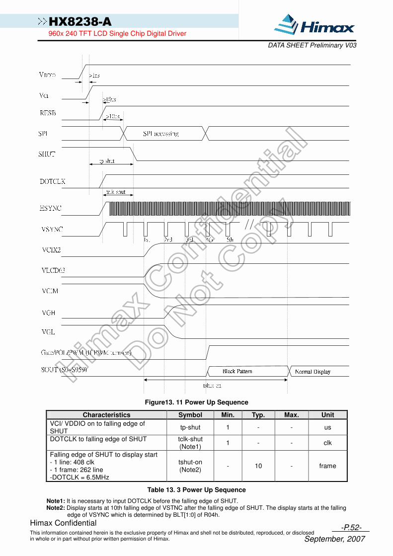
-P.52- This information contained herein is the exclusive property of Himax and shell not be distributed, reproduced, or disclosed in whole or in part without prior written permission of Himax.
Himax Confidential
September, 2007
HX8238-A 960x 240 TFT LCD Single Chip Digital Driver
DATA SHEET Preliminary V03
RESBSHUTHSYNC
>10us>1ns
DOTCLKVSYNC 1st
SPI SPI accessingVCIVDDIO>10us
tp-shuttclk-shutVCIX2VLCD63VCIMVGHVGLGate/POL/PWM (If PWM turn-on)SOUT (S0~S959) tshut-on
2nd 3rd 4th 5th
Figure13. 11 Power Up Sequence
Characteristics Symbol Min. Typ. Max. Unit
VCI/ VDDIO on to falling edge of SHUT
tp-shut 1 - - us
DOTCLK to falling edge of SHUT tclk-shut (Note1)
1 - - clk
Falling edge of SHUT to display start - 1 line: 408 clk - 1 frame: 262 line -DOTCLK = 6.5MHz
tshut-on (Note2)
- 10 - frame
Table 13. 3 Power Up Sequence
Note1: It is necessary to input DOTCLK before the falling edge of SHUT. Note2: Display starts at 10th falling edge of VSTNC after the falling edge of SHUT. The display starts at the falling
edge of VSYNC which is determined by BLT[1:0] of R04h.

-P.53- This information contained herein is the exclusive property of Himax and shell not be distributed, reproduced, or disclosed in whole or in part without prior written permission of Himax.
Himax Confidential
September, 2007
HX8238-A 960x 240 TFT LCD Single Chip Digital Driver
DATA SHEET Preliminary V03
RESBHSYNCDOTCLKVSYNCSPI SPI accessingVCIVDDIO
VCIX2VLCD63VCIMVGHVGLGate/POL/PWM (If PWM turn-on)SOUT (S0~S959) tshut-off
SHUT1st 2nd 3rd 4th 5th 6th
VGL discharge to groundFloatingFloatingFloatingFloating
Figure13. 12 Power Down Sequence
Characteristics Symbol Min. Typ. Max. Unit
Rising edge of SHUT to display off - 1 line: 408 clk - 1 frame: 262 line - DOTCLK = 6.5MHz
tshut-off - - 6 frame
Note: DOTCLK must be maintained at lease 6 frames after the rising edge of SHUT.
Display become off at the 6nd falling edge of VSTNC after the falling edge of SHUT. If RESET signal is necessary for power down, provide it after the 6-frames-cycle of the SHUT period.
Table 13. 4 Power Down Sequence

-P.54- This information contained herein is the exclusive property of Himax and shell not be distributed, reproduced, or disclosed in whole or in part without prior written permission of Himax.
Himax Confidential
September, 2007
HX8238-A 960x 240 TFT LCD Single Chip Digital Driver
DATA SHEET Preliminary V03
Write SPI
tcss
tclk tsl tsh
tcsh
tcsd
tds
tdh
1 2 3 4 5 6 7 8 9 10 11 12 13 14 15 16 17 18 19 20 21 22 23 24
0 1 R/S R/W
First Transmission (Register)
CSB
SCL
SDI
Second Transmission (Data )
1 2 3 4 5 6 7 8 9 10 11 12 13 14 15 16 17 18 19 20 21 22 23 24
0 1 1 1 0 0 R/S R/W 0 0 0 1 0 0 1 0 0 1 1 0 0 1 0 0
CSB
SCL
SDI
1 1 0 0 0 0 0 0 0 0 0 0 0 0 1 0 1 0 0 0
Note: The example writes “0x1264h” to register R28h.
SPID connected to VSS.
Figure13. 13 SPI interface Timing Diagram & Write SPI Example

-P.55- This information contained herein is the exclusive property of Himax and shell not be distributed, reproduced, or disclosed in whole or in part without prior written permission of Himax.
Himax Confidential
September, 2007
HX8238-A 960x 240 TFT LCD Single Chip Digital Driver
DATA SHEET Preliminary V03
Read SPI
1 2 3 4 5 6 7 8 9 10 11 12 13 14 15 16 17 18 19 20 21 22 23 24
SCL
SDO
CSB
SDI0 1 1 1 0 0 R/S R/W
0 0 0 1 0 0 1 0 0 1 1 0 0 1 0 0
1 2 3 4 5 6 7 8 9 10 11 12 13 14 15 16 17 18 19 20 21 22 23 24
SCL
CSB
SDI0 1 1 1 0 0 R/S R/W 0 0 0 0 0 0 0 0 0 0 1 0 1 0 0 0
First Transmission (Register)
Second Transmission (Data)
Note: The example Read “0x1264h” from register R28h.
Figure13. 14 SPI interface Timing Diagram & Read SPI Example
Figure13. 15 Rising/Falling time
Characteristics Symbol Min. Typ. Max. Unit
Serial Clock Frequency fclk - - 20 MHz
Serial Clock Cycle Time tclk 50 - - ns
Clock Low Width tsl 25 - - ns
Clock High Width tsh 25 - - ns
Clock Rising Time trs - - 30 ns
Clock Falling Time tfl - - 30 ns
Chip Select Setup Time tcss 0 - - ns
Chip Select Hold Time tcsh 10 - - ns
Chip Select High Delay Time tcsd 20 - - ns
Data Setup Time tds 5 - - ns
Data Hold Time tdh 10 - - ns
Table 13. 5 SPI Timing

-P.56- This information contained herein is the exclusive property of Himax and shell not be distributed, reproduced, or disclosed in whole or in part without prior written permission of Himax.
Himax Confidential
September, 2007
HX8238-A 960x 240 TFT LCD Single Chip Digital Driver
DATA SHEET Preliminary V03
14. HX8238-A Output Voltage Relationship
VGH(9.3~16.5V)
VLCD63( MAX 5.57V)
VCI (2.5~3.6V)
VCOMH ( MAX 5.54V)
VCOML
VGL (-5.9~-15V)
VCIX2
VCIM
VSS
Note: The above voltages level assumed 100% efficiency of the internal booster. There has no voltage drop due to
resistance from ITO trace of the panel.
Figure 14. 1 LCD Driving Voltage Relationship

-P.57- This information contained herein is the exclusive property of Himax and shell not be distributed, reproduced, or disclosed in whole or in part without prior written permission of Himax.
Himax Confidential
September, 2007
HX8238-A 960x 240 TFT LCD Single Chip Digital Driver
DATA SHEET Preliminary V03
15. Application Circuit
CXP
CXN
CYP
CYN
C1P
C1N
C2P
C2N
C3P
C3N
CP
CN
10V
10V
10V
25V
All capacitors
are ceramic
0.1~0.33uF
25V
25V
Figure 15. 1 Booster Capacitors
REGVDD = VDDIO
REGVDD = VSS
Regulator
VDD
VDDIO
VCI
REGVDD
VSS
System Vdd
Analog power
2.5~3.6V
Regulator
VDD
VDDIO
VCI
REGVDD
VSS
System Vdd
Analog power
2.5~3.6V
2.2uF/ 6.3V 2.2uF/ 6.3V
System Vdd > 2.5V 2.5V ≧ System Vdd ≧ 1.8V
Figure 15. 2 Power Supply Pins Connections
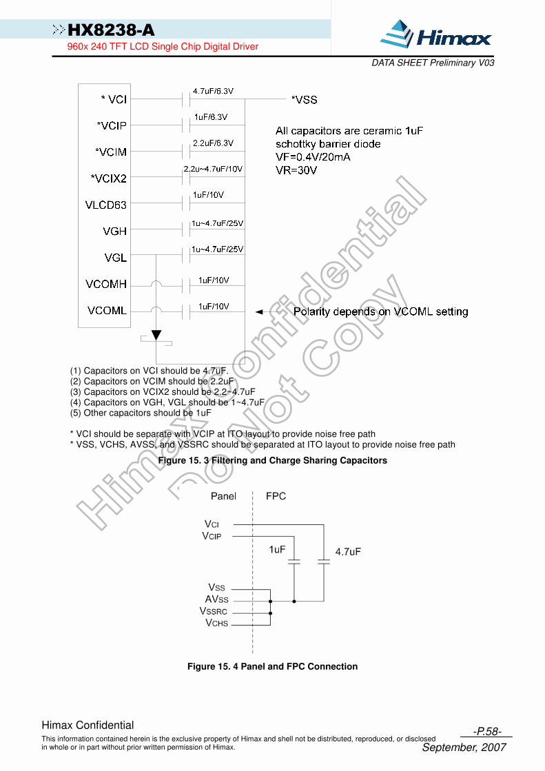
-P.58- This information contained herein is the exclusive property of Himax and shell not be distributed, reproduced, or disclosed in whole or in part without prior written permission of Himax.
Himax Confidential
September, 2007
HX8238-A 960x 240 TFT LCD Single Chip Digital Driver
DATA SHEET Preliminary V03
(1) Capacitors on VCI should be 4.7uF. (2) Capacitors on VCIM should be 2.2uF (3) Capacitors on VCIX2 should be 2.2~4.7uF (4) Capacitors on VGH, VGL should be 1~4.7uF (5) Other capacitors should be 1uF
* VCI should be separate with VCIP at ITO layout to provide noise free path * VSS, VCHS, AVSS, and VSSRC should be separated at ITO layout to provide noise free path
Figure 15. 3 Filtering and Charge Sharing Capacitors
Figure 15. 4 Panel and FPC Connection

-P.59- This information contained herein is the exclusive property of Himax and shell not be distributed, reproduced, or disclosed in whole or in part without prior written permission of Himax.
Himax Confidential
September, 2007
HX8238-A 960x 240 TFT LCD Single Chip Digital Driver
DATA SHEET Preliminary V03
960 X 240
TFT Panel
Cs on Common
960
240
Figure 15. 5 Panel Connection Example
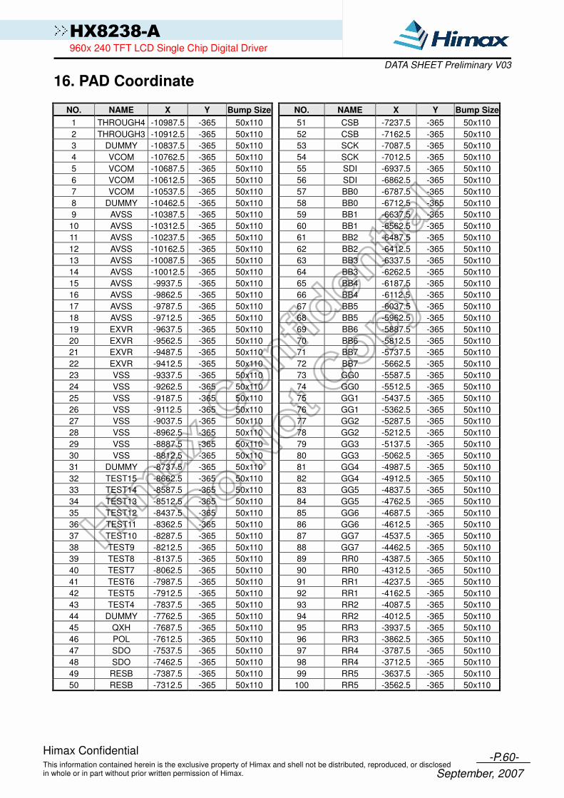
-P.60- This information contained herein is the exclusive property of Himax and shell not be distributed, reproduced, or disclosed in whole or in part without prior written permission of Himax.
Himax Confidential
September, 2007
HX8238-A 960x 240 TFT LCD Single Chip Digital Driver
DATA SHEET Preliminary V03
16. PAD Coordinate
NO. NAME X Y Bump Size NO. NAME X Y Bump Size
1 THROUGH4 -10987.5 -365 50x110 51 CSB -7237.5 -365 50x110
2 THROUGH3 -10912.5 -365 50x110 52 CSB -7162.5 -365 50x110
3 DUMMY -10837.5 -365 50x110 53 SCK -7087.5 -365 50x110
4 VCOM -10762.5 -365 50x110 54 SCK -7012.5 -365 50x110
5 VCOM -10687.5 -365 50x110 55 SDI -6937.5 -365 50x110
6 VCOM -10612.5 -365 50x110 56 SDI -6862.5 -365 50x110
7 VCOM -10537.5 -365 50x110 57 BB0 -6787.5 -365 50x110
8 DUMMY -10462.5 -365 50x110 58 BB0 -6712.5 -365 50x110
9 AVSS -10387.5 -365 50x110 59 BB1 -6637.5 -365 50x110
10 AVSS -10312.5 -365 50x110 60 BB1 -6562.5 -365 50x110
11 AVSS -10237.5 -365 50x110 61 BB2 -6487.5 -365 50x110
12 AVSS -10162.5 -365 50x110 62 BB2 -6412.5 -365 50x110
13 AVSS -10087.5 -365 50x110 63 BB3 -6337.5 -365 50x110
14 AVSS -10012.5 -365 50x110 64 BB3 -6262.5 -365 50x110
15 AVSS -9937.5 -365 50x110 65 BB4 -6187.5 -365 50x110
16 AVSS -9862.5 -365 50x110 66 BB4 -6112.5 -365 50x110
17 AVSS -9787.5 -365 50x110 67 BB5 -6037.5 -365 50x110
18 AVSS -9712.5 -365 50x110 68 BB5 -5962.5 -365 50x110
19 EXVR -9637.5 -365 50x110 69 BB6 -5887.5 -365 50x110
20 EXVR -9562.5 -365 50x110 70 BB6 -5812.5 -365 50x110
21 EXVR -9487.5 -365 50x110 71 BB7 -5737.5 -365 50x110
22 EXVR -9412.5 -365 50x110 72 BB7 -5662.5 -365 50x110
23 VSS -9337.5 -365 50x110 73 GG0 -5587.5 -365 50x110
24 VSS -9262.5 -365 50x110 74 GG0 -5512.5 -365 50x110
25 VSS -9187.5 -365 50x110 75 GG1 -5437.5 -365 50x110
26 VSS -9112.5 -365 50x110 76 GG1 -5362.5 -365 50x110
27 VSS -9037.5 -365 50x110 77 GG2 -5287.5 -365 50x110
28 VSS -8962.5 -365 50x110 78 GG2 -5212.5 -365 50x110
29 VSS -8887.5 -365 50x110 79 GG3 -5137.5 -365 50x110
30 VSS -8812.5 -365 50x110 80 GG3 -5062.5 -365 50x110
31 DUMMY -8737.5 -365 50x110 81 GG4 -4987.5 -365 50x110
32 TEST15 -8662.5 -365 50x110 82 GG4 -4912.5 -365 50x110
33 TEST14 -8587.5 -365 50x110 83 GG5 -4837.5 -365 50x110
34 TEST13 -8512.5 -365 50x110 84 GG5 -4762.5 -365 50x110
35 TEST12 -8437.5 -365 50x110 85 GG6 -4687.5 -365 50x110
36 TEST11 -8362.5 -365 50x110 86 GG6 -4612.5 -365 50x110
37 TEST10 -8287.5 -365 50x110 87 GG7 -4537.5 -365 50x110
38 TEST9 -8212.5 -365 50x110 88 GG7 -4462.5 -365 50x110
39 TEST8 -8137.5 -365 50x110 89 RR0 -4387.5 -365 50x110
40 TEST7 -8062.5 -365 50x110 90 RR0 -4312.5 -365 50x110
41 TEST6 -7987.5 -365 50x110 91 RR1 -4237.5 -365 50x110
42 TEST5 -7912.5 -365 50x110 92 RR1 -4162.5 -365 50x110
43 TEST4 -7837.5 -365 50x110 93 RR2 -4087.5 -365 50x110
44 DUMMY -7762.5 -365 50x110 94 RR2 -4012.5 -365 50x110
45 QXH -7687.5 -365 50x110 95 RR3 -3937.5 -365 50x110
46 POL -7612.5 -365 50x110 96 RR3 -3862.5 -365 50x110
47 SDO -7537.5 -365 50x110 97 RR4 -3787.5 -365 50x110
48 SDO -7462.5 -365 50x110 98 RR4 -3712.5 -365 50x110
49 RESB -7387.5 -365 50x110 99 RR5 -3637.5 -365 50x110
50 RESB -7312.5 -365 50x110 100 RR5 -3562.5 -365 50x110

-P.61- This information contained herein is the exclusive property of Himax and shell not be distributed, reproduced, or disclosed in whole or in part without prior written permission of Himax.
Himax Confidential
September, 2007
HX8238-A 960x 240 TFT LCD Single Chip Digital Driver
DATA SHEET Preliminary V03
NO. NAME X Y Bump Size NO. NAME X Y Bump Size
101 RR6 -3487.5 -365 50x110 151 C1N 262.5 -365 50x110
102 RR6 -3412.5 -365 50x110 152 C1N 337.5 -365 50x110
103 RR7 -3337.5 -365 50x110 153 C1N 412.5 -365 50x110
104 RR7 -3262.5 -365 50x110 154 C1N 487.5 -365 50x110
105 DEN -3187.5 -365 50x110 155 C1N 562.5 -365 50x110
106 DEN -3112.5 -365 50x110 156 VLCD63 637.5 -365 50x110
107 HSYNC -3037.5 -365 50x110 157 VLCD63 712.5 -365 50x110
108 HSYNC -2962.5 -365 50x110 158 VLCD63 787.5 -365 50x110
109 VSYNC -2887.5 -365 50x110 159 VLCD63 862.5 -365 50x110
110 VSYNC -2812.5 -365 50x110 160 VLCD63 937.5 -365 50x110
111 DOTCLK -2737.5 -365 50x110 161 VLCD63 1012.5 -365 50x110
112 DOTCLK -2662.5 -365 50x110 162 VCIX2J 1087.5 -365 50x110
113 SHUT -2587.5 -365 50x110 163 VCIX2J 1162.5 -365 50x110
114 SHUT -2512.5 -365 50x110 164 VCIX2J 1237.5 -365 50x110
115 VSS -2437.5 -365 50x110 165 VCIX2J 1312.5 -365 50x110
116 TB -2362.5 -365 50x110 166 VCIX2J 1387.5 -365 50x110
117 VDDIO -2287.5 -365 50x110 167 VCIX2J 1462.5 -365 50x110
118 REV -2212.5 -365 50x110 168 VCIX2 1537.5 -365 50x110
119 VSS -2137.5 -365 50x110 169 VCIX2 1612.5 -365 50x110
120 REGVDD -2062.5 -365 50x110 170 VCIX2 1687.5 -365 50x110
121 VDDIO -1987.5 -365 50x110 171 VCIX2 1762.5 -365 50x110
122 RL -1912.5 -365 50x110 172 VCIX2 1837.5 -365 50x110
123 VSS -1837.5 -365 50x110 173 VCIX2 1912.5 -365 50x110
124 CM -1762.5 -365 50x110 174 CYN 1987.5 -365 50x110
125 VDDIO -1687.5 -365 50x110 175 CYN 2062.5 -365 50x110
126 BGR -1612.5 -365 50x110 176 CYN 2137.5 -365 50x110
127 VSS -1537.5 -365 50x110 177 CYN 2212.5 -365 50x110
128 SEL0 -1462.5 -365 50x110 178 CYN 2287.5 -365 50x110
129 SEL1 -1387.5 -365 50x110 179 CYN 2362.5 -365 50x110
130 SEL2 -1312.5 -365 50x110 180 CYP 2437.5 -365 50x110
131 VDDIO -1237.5 -365 50x110 181 CYP 2512.5 -365 50x110
132 SWD0 -1162.5 -365 50x110 182 CYP 2587.5 -365 50x110
133 VSS -1087.5 -365 50x110 183 CYP 2662.5 -365 50x110
134 SWD1 -1012.5 -365 50x110 184 CYP 2737.5 -365 50x110
135 VDDIO -937.5 -365 50x110 185 CYP 2812.5 -365 50x110
136 SWD2 -862.5 -365 50x110 186 CXN 2887.5 -365 50x110
137 VSS -787.5 -365 50x110 187 CXN 2962.5 -365 50x110
138 CPE -712.5 -365 50x110 188 CXN 3037.5 -365 50x110
139 PINV -637.5 -365 50x110 189 CXN 3112.5 -365 50x110
140 DUMMY -562.5 -365 50x110 190 CXN 3187.5 -365 50x110
141 VCIM -487.5 -365 50x110 191 CXN 3262.5 -365 50x110
142 VCIM -412.5 -365 50x110 192 CXP 3337.5 -365 50x110
143 VCIM -337.5 -365 50x110 193 CXP 3412.5 -365 50x110
144 VCIM -262.5 -365 50x110 194 CXP 3487.5 -365 50x110
145 VCIM -187.5 -365 50x110 195 CXP 3562.5 -365 50x110
146 C1P -112.5 -365 50x110 196 CXP 3637.5 -365 50x110
147 C1P -37.5 -365 50x110 197 CXP 3712.5 -365 50x110
148 C1P 37.5 -365 50x110 198 VDDIO 3787.5 -365 50x110
149 C1P 112.5 -365 50x110 199 VDDIO 3862.5 -365 50x110
150 C1P 187.5 -365 50x110 200 VDDIO 3937.5 -365 50x110

-P.62- This information contained herein is the exclusive property of Himax and shell not be distributed, reproduced, or disclosed in whole or in part without prior written permission of Himax.
Himax Confidential
September, 2007
HX8238-A 960x 240 TFT LCD Single Chip Digital Driver
DATA SHEET Preliminary V03
NO. NAME X Y Bump Size NO. NAME X Y Bump Size
201 VDDIO 4012.5 -365 50x110 251 VGH 7762.5 -365 50x110
202 VDDIO 4087.5 -365 50x110 252 VGH 7837.5 -365 50x110
203 VDDIO 4162.5 -365 50x110 253 TEST17 7912.5 -365 50x110
204 VCIP 4237.5 -365 50x110 254 TEST16 7987.5 -365 50x110
205 VCIP 4312.5 -365 50x110 255 VCOMR 8062.5 -365 50x110
206 VCIP 4387.5 -365 50x110 256 VCOMR 8137.5 -365 50x110
207 VCIP 4462.5 -365 50x110 257 VCOML 8212.5 -365 50x110
208 VCI 4537.5 -365 50x110 258 VCOML 8287.5 -365 50x110
209 VCI 4612.5 -365 50x110 259 VCOML 8362.5 -365 50x110
210 VCI 4687.5 -365 50x110 260 VCOML 8437.5 -365 50x110
211 VCI 4762.5 -365 50x110 261 VCOMH 8512.5 -365 50x110
212 VCI 4837.5 -365 50x110 262 VCOMH 8587.5 -365 50x110
213 VCI 4912.5 -365 50x110 263 VCOMH 8662.5 -365 50x110
214 VCI 4987.5 -365 50x110 264 VCOMH 8737.5 -365 50x110
215 VCI 5062.5 -365 50x110 265 VCOM 8812.5 -365 50x110
216 VCI 5137.5 -365 50x110 266 VCOM 8887.5 -365 50x110
217 VCI 5212.5 -365 50x110 267 VCOM 8962.5 -365 50x110
218 VDD 5287.5 -365 50x110 268 VCOM 9037.5 -365 50x110
219 VDD 5362.5 -365 50x110 269 VSSRC 9112.5 -365 50x110
220 VDD 5437.5 -365 50x110 270 VSSRC 9187.5 -365 50x110
221 VDD 5512.5 -365 50x110 271 VSSRC 9262.5 -365 50x110
222 VDD 5587.5 -365 50x110 272 VSSRC 9337.5 -365 50x110
223 VDD 5662.5 -365 50x110 273 VSSRC 9412.5 -365 50x110
224 DUMMY 5737.5 -365 50x110 274 VSSRC 9487.5 -365 50x110
225 CN 5812.5 -365 50x110 275 VSSRC 9562.5 -365 50x110
226 CN 5887.5 -365 50x110 276 VSSRC 9637.5 -365 50x110
227 CN 5962.5 -365 50x110 277 VCHS 9712.5 -365 50x110
228 CP 6037.5 -365 50x110 278 VCHS 9787.5 -365 50x110
229 CP 6112.5 -365 50x110 279 VCHS 9862.5 -365 50x110
230 CP 6187.5 -365 50x110 280 VCHS 9937.5 -365 50x110
231 VGL 6262.5 -365 50x110 281 VCHS 10012.5 -365 50x110
232 VGL 6337.5 -365 50x110 282 VCHS 10087.5 -365 50x110
233 VGL 6412.5 -365 50x110 283 VCHS 10162.5 -365 50x110
234 VGL 6487.5 -365 50x110 284 VCHS 10237.5 -365 50x110
235 VGL 6562.5 -365 50x110 285 VCHS 10312.5 -365 50x110
236 C2N 6637.5 -365 50x110 286 VCHS 10387.5 -365 50x110
237 C2N 6712.5 -365 50x110 287 DUMMY 10462.5 -365 50x110
238 C2N 6787.5 -365 50x110 288 VFB 10537.5 -365 50x110
239 C2P 6862.5 -365 50x110 289 VFB 10612.5 -365 50x110
240 C2P 6937.5 -365 50x110 290 DRV 10687.5 -365 50x110
241 C2P 7012.5 -365 50x110 291 DRV 10762.5 -365 50x110
242 C3N 7087.5 -365 50x110 292 DUMMY 10837.5 -365 50x110
243 C3N 7162.5 -365 50x110 293 THROUGH2 10912.5 -365 50x110
244 C3N 7237.5 -365 50x110 294 THROUGH1 10987.5 -365 50x110
245 C3P 7312.5 -365 50x110 295 R_MARK 10967.5 -145 NA
246 C3P 7387.5 -365 50x110 296 DUMMY 11016 370 18x100
247 C3P 7462.5 -365 50x110 297 THROUGH5 10998 240 18x100
248 VGH 7537.5 -365 50x110 298 THROUGH6 10980 370 18x100
249 VGH 7612.5 -365 50x110 299 DUMMY 10962 240 18x100
250 VGH 7687.5 -365 50x110 300 DUMMY 10944 370 18x100
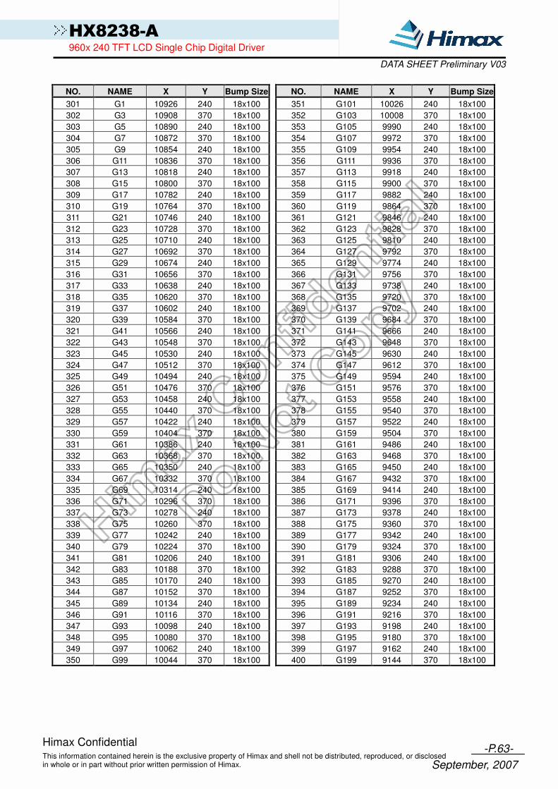
-P.63- This information contained herein is the exclusive property of Himax and shell not be distributed, reproduced, or disclosed in whole or in part without prior written permission of Himax.
Himax Confidential
September, 2007
HX8238-A 960x 240 TFT LCD Single Chip Digital Driver
DATA SHEET Preliminary V03
NO. NAME X Y Bump Size NO. NAME X Y Bump Size
301 G1 10926 240 18x100 351 G101 10026 240 18x100
302 G3 10908 370 18x100 352 G103 10008 370 18x100
303 G5 10890 240 18x100 353 G105 9990 240 18x100
304 G7 10872 370 18x100 354 G107 9972 370 18x100
305 G9 10854 240 18x100 355 G109 9954 240 18x100
306 G11 10836 370 18x100 356 G111 9936 370 18x100
307 G13 10818 240 18x100 357 G113 9918 240 18x100
308 G15 10800 370 18x100 358 G115 9900 370 18x100
309 G17 10782 240 18x100 359 G117 9882 240 18x100
310 G19 10764 370 18x100 360 G119 9864 370 18x100
311 G21 10746 240 18x100 361 G121 9846 240 18x100
312 G23 10728 370 18x100 362 G123 9828 370 18x100
313 G25 10710 240 18x100 363 G125 9810 240 18x100
314 G27 10692 370 18x100 364 G127 9792 370 18x100
315 G29 10674 240 18x100 365 G129 9774 240 18x100
316 G31 10656 370 18x100 366 G131 9756 370 18x100
317 G33 10638 240 18x100 367 G133 9738 240 18x100
318 G35 10620 370 18x100 368 G135 9720 370 18x100
319 G37 10602 240 18x100 369 G137 9702 240 18x100
320 G39 10584 370 18x100 370 G139 9684 370 18x100
321 G41 10566 240 18x100 371 G141 9666 240 18x100
322 G43 10548 370 18x100 372 G143 9648 370 18x100
323 G45 10530 240 18x100 373 G145 9630 240 18x100
324 G47 10512 370 18x100 374 G147 9612 370 18x100
325 G49 10494 240 18x100 375 G149 9594 240 18x100
326 G51 10476 370 18x100 376 G151 9576 370 18x100
327 G53 10458 240 18x100 377 G153 9558 240 18x100
328 G55 10440 370 18x100 378 G155 9540 370 18x100
329 G57 10422 240 18x100 379 G157 9522 240 18x100
330 G59 10404 370 18x100 380 G159 9504 370 18x100
331 G61 10386 240 18x100 381 G161 9486 240 18x100
332 G63 10368 370 18x100 382 G163 9468 370 18x100
333 G65 10350 240 18x100 383 G165 9450 240 18x100
334 G67 10332 370 18x100 384 G167 9432 370 18x100
335 G69 10314 240 18x100 385 G169 9414 240 18x100
336 G71 10296 370 18x100 386 G171 9396 370 18x100
337 G73 10278 240 18x100 387 G173 9378 240 18x100
338 G75 10260 370 18x100 388 G175 9360 370 18x100
339 G77 10242 240 18x100 389 G177 9342 240 18x100
340 G79 10224 370 18x100 390 G179 9324 370 18x100
341 G81 10206 240 18x100 391 G181 9306 240 18x100
342 G83 10188 370 18x100 392 G183 9288 370 18x100
343 G85 10170 240 18x100 393 G185 9270 240 18x100
344 G87 10152 370 18x100 394 G187 9252 370 18x100
345 G89 10134 240 18x100 395 G189 9234 240 18x100
346 G91 10116 370 18x100 396 G191 9216 370 18x100
347 G93 10098 240 18x100 397 G193 9198 240 18x100
348 G95 10080 370 18x100 398 G195 9180 370 18x100
349 G97 10062 240 18x100 399 G197 9162 240 18x100
350 G99 10044 370 18x100 400 G199 9144 370 18x100

-P.64- This information contained herein is the exclusive property of Himax and shell not be distributed, reproduced, or disclosed in whole or in part without prior written permission of Himax.
Himax Confidential
September, 2007
HX8238-A 960x 240 TFT LCD Single Chip Digital Driver
DATA SHEET Preliminary V03
NO. NAME X Y Bump Size NO. NAME X Y Bump Size
401 G201 9126 240 18x100 451 S24 8226 240 18x100
402 G203 9108 370 18x100 452 S25 8208 370 18x100
403 G205 9090 240 18x100 453 S26 8190 240 18x100
404 G207 9072 370 18x100 454 S27 8172 370 18x100
405 G209 9054 240 18x100 455 S28 8154 240 18x100
406 G211 9036 370 18x100 456 S29 8136 370 18x100
407 G213 9018 240 18x100 457 S30 8118 240 18x100
408 G215 9000 370 18x100 458 S31 8100 370 18x100
409 G217 8982 240 18x100 459 S32 8082 240 18x100
410 G219 8964 370 18x100 460 S33 8064 370 18x100
411 G221 8946 240 18x100 461 S34 8046 240 18x100
412 G223 8928 370 18x100 462 S35 8028 370 18x100
413 G225 8910 240 18x100 463 S36 8010 240 18x100
414 G227 8892 370 18x100 464 S37 7992 370 18x100
415 G229 8874 240 18x100 465 S38 7974 240 18x100
416 G231 8856 370 18x100 466 S39 7956 370 18x100
417 G233 8838 240 18x100 467 S40 7938 240 18x100
418 G235 8820 370 18x100 468 S41 7920 370 18x100
419 G237 8802 240 18x100 469 S42 7902 240 18x100
420 G239 8784 370 18x100 470 S43 7884 370 18x100
421 DUMMY 8766 240 18x100 471 S44 7866 240 18x100
422 DUMMY 8748 370 18x100 472 S45 7848 370 18x100
423 DUMMY 8730 240 18x100 473 S46 7830 240 18x100
424 DUMMY 8712 370 18x100 474 S47 7812 370 18x100
425 DUMMY 8694 240 18x100 475 S48 7794 240 18x100
426 DUMMY 8676 370 18x100 476 S49 7776 370 18x100
427 S0 8658 240 18x100 477 S50 7758 240 18x100
428 S1 8640 370 18x100 478 S51 7740 370 18x100
429 S2 8622 240 18x100 479 S52 7722 240 18x100
430 S3 8604 370 18x100 480 S53 7704 370 18x100
431 S4 8586 240 18x100 481 S54 7686 240 18x100
432 S5 8568 370 18x100 482 S55 7668 370 18x100
433 S6 8550 240 18x100 483 S56 7650 240 18x100
434 S7 8532 370 18x100 484 S57 7632 370 18x100
435 S8 8514 240 18x100 485 S58 7614 240 18x100
436 S9 8496 370 18x100 486 S59 7596 370 18x100
437 S10 8478 240 18x100 487 S60 7578 240 18x100
438 S11 8460 370 18x100 488 S61 7560 370 18x100
439 S12 8442 240 18x100 489 S62 7542 240 18x100
440 S13 8424 370 18x100 490 S63 7524 370 18x100
441 S14 8406 240 18x100 491 S64 7506 240 18x100
442 S15 8388 370 18x100 492 S65 7488 370 18x100
443 S16 8370 240 18x100 493 S66 7470 240 18x100
444 S17 8352 370 18x100 494 S67 7452 370 18x100
445 S18 8334 240 18x100 495 S68 7434 240 18x100
446 S19 8316 370 18x100 496 S69 7416 370 18x100
447 S20 8298 240 18x100 497 S70 7398 240 18x100
448 S21 8280 370 18x100 498 S71 7380 370 18x100
449 S22 8262 240 18x100 499 S72 7362 240 18x100
450 S23 8244 370 18x100 500 S73 7344 370 18x100
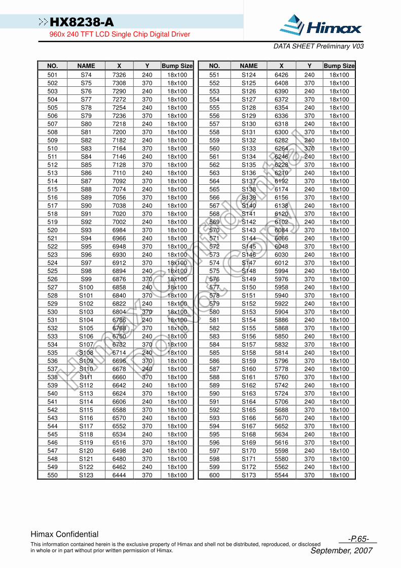
-P.65- This information contained herein is the exclusive property of Himax and shell not be distributed, reproduced, or disclosed in whole or in part without prior written permission of Himax.
Himax Confidential
September, 2007
HX8238-A 960x 240 TFT LCD Single Chip Digital Driver
DATA SHEET Preliminary V03
NO. NAME X Y Bump Size NO. NAME X Y Bump Size
501 S74 7326 240 18x100 551 S124 6426 240 18x100
502 S75 7308 370 18x100 552 S125 6408 370 18x100
503 S76 7290 240 18x100 553 S126 6390 240 18x100
504 S77 7272 370 18x100 554 S127 6372 370 18x100
505 S78 7254 240 18x100 555 S128 6354 240 18x100
506 S79 7236 370 18x100 556 S129 6336 370 18x100
507 S80 7218 240 18x100 557 S130 6318 240 18x100
508 S81 7200 370 18x100 558 S131 6300 370 18x100
509 S82 7182 240 18x100 559 S132 6282 240 18x100
510 S83 7164 370 18x100 560 S133 6264 370 18x100
511 S84 7146 240 18x100 561 S134 6246 240 18x100
512 S85 7128 370 18x100 562 S135 6228 370 18x100
513 S86 7110 240 18x100 563 S136 6210 240 18x100
514 S87 7092 370 18x100 564 S137 6192 370 18x100
515 S88 7074 240 18x100 565 S138 6174 240 18x100
516 S89 7056 370 18x100 566 S139 6156 370 18x100
517 S90 7038 240 18x100 567 S140 6138 240 18x100
518 S91 7020 370 18x100 568 S141 6120 370 18x100
519 S92 7002 240 18x100 569 S142 6102 240 18x100
520 S93 6984 370 18x100 570 S143 6084 370 18x100
521 S94 6966 240 18x100 571 S144 6066 240 18x100
522 S95 6948 370 18x100 572 S145 6048 370 18x100
523 S96 6930 240 18x100 573 S146 6030 240 18x100
524 S97 6912 370 18x100 574 S147 6012 370 18x100
525 S98 6894 240 18x100 575 S148 5994 240 18x100
526 S99 6876 370 18x100 576 S149 5976 370 18x100
527 S100 6858 240 18x100 577 S150 5958 240 18x100
528 S101 6840 370 18x100 578 S151 5940 370 18x100
529 S102 6822 240 18x100 579 S152 5922 240 18x100
530 S103 6804 370 18x100 580 S153 5904 370 18x100
531 S104 6786 240 18x100 581 S154 5886 240 18x100
532 S105 6768 370 18x100 582 S155 5868 370 18x100
533 S106 6750 240 18x100 583 S156 5850 240 18x100
534 S107 6732 370 18x100 584 S157 5832 370 18x100
535 S108 6714 240 18x100 585 S158 5814 240 18x100
536 S109 6696 370 18x100 586 S159 5796 370 18x100
537 S110 6678 240 18x100 587 S160 5778 240 18x100
538 S111 6660 370 18x100 588 S161 5760 370 18x100
539 S112 6642 240 18x100 589 S162 5742 240 18x100
540 S113 6624 370 18x100 590 S163 5724 370 18x100
541 S114 6606 240 18x100 591 S164 5706 240 18x100
542 S115 6588 370 18x100 592 S165 5688 370 18x100
543 S116 6570 240 18x100 593 S166 5670 240 18x100
544 S117 6552 370 18x100 594 S167 5652 370 18x100
545 S118 6534 240 18x100 595 S168 5634 240 18x100
546 S119 6516 370 18x100 596 S169 5616 370 18x100
547 S120 6498 240 18x100 597 S170 5598 240 18x100
548 S121 6480 370 18x100 598 S171 5580 370 18x100
549 S122 6462 240 18x100 599 S172 5562 240 18x100
550 S123 6444 370 18x100 600 S173 5544 370 18x100

-P.66- This information contained herein is the exclusive property of Himax and shell not be distributed, reproduced, or disclosed in whole or in part without prior written permission of Himax.
Himax Confidential
September, 2007
HX8238-A 960x 240 TFT LCD Single Chip Digital Driver
DATA SHEET Preliminary V03
NO. NAME X Y Bump Size NO. NAME X Y Bump Size
601 S174 5526 240 18x100 651 S224 4626 240 18x100
602 S175 5508 370 18x100 652 S225 4608 370 18x100
603 S176 5490 240 18x100 653 S226 4590 240 18x100
604 S177 5472 370 18x100 654 S227 4572 370 18x100
605 S178 5454 240 18x100 655 S228 4554 240 18x100
606 S179 5436 370 18x100 656 S229 4536 370 18x100
607 S180 5418 240 18x100 657 S230 4518 240 18x100
608 S181 5400 370 18x100 658 S231 4500 370 18x100
609 S182 5382 240 18x100 659 S232 4482 240 18x100
610 S183 5364 370 18x100 660 S233 4464 370 18x100
611 S184 5346 240 18x100 661 S234 4446 240 18x100
612 S185 5328 370 18x100 662 S235 4428 370 18x100
613 S186 5310 240 18x100 663 S236 4410 240 18x100
614 S187 5292 370 18x100 664 S237 4392 370 18x100
615 S188 5274 240 18x100 665 S238 4374 240 18x100
616 S189 5256 370 18x100 666 S239 4356 370 18x100
617 S190 5238 240 18x100 667 S240 4338 240 18x100
618 S191 5220 370 18x100 668 S241 4320 370 18x100
619 S192 5202 240 18x100 669 S242 4302 240 18x100
620 S193 5184 370 18x100 670 S243 4284 370 18x100
621 S194 5166 240 18x100 671 S244 4266 240 18x100
622 S195 5148 370 18x100 672 S245 4248 370 18x100
623 S196 5130 240 18x100 673 S246 4230 240 18x100
624 S197 5112 370 18x100 674 S247 4212 370 18x100
625 S198 5094 240 18x100 675 S248 4194 240 18x100
626 S199 5076 370 18x100 676 S249 4176 370 18x100
627 S200 5058 240 18x100 677 S250 4158 240 18x100
628 S201 5040 370 18x100 678 S251 4140 370 18x100
629 S202 5022 240 18x100 679 S252 4122 240 18x100
630 S203 5004 370 18x100 680 S253 4104 370 18x100
631 S204 4986 240 18x100 681 S254 4086 240 18x100
632 S205 4968 370 18x100 682 S255 4068 370 18x100
633 S206 4950 240 18x100 683 S256 4050 240 18x100
634 S207 4932 370 18x100 684 S257 4032 370 18x100
635 S208 4914 240 18x100 685 S258 4014 240 18x100
636 S209 4896 370 18x100 686 S259 3996 370 18x100
637 S210 4878 240 18x100 687 S260 3978 240 18x100
638 S211 4860 370 18x100 688 S261 3960 370 18x100
639 S212 4842 240 18x100 689 S262 3942 240 18x100
640 S213 4824 370 18x100 690 S263 3924 370 18x100
641 S214 4806 240 18x100 691 S264 3906 240 18x100
642 S215 4788 370 18x100 692 S265 3888 370 18x100
643 S216 4770 240 18x100 693 S266 3870 240 18x100
644 S217 4752 370 18x100 694 S267 3852 370 18x100
645 S218 4734 240 18x100 695 S268 3834 240 18x100
646 S219 4716 370 18x100 696 S269 3816 370 18x100
647 S220 4698 240 18x100 697 S270 3798 240 18x100
648 S221 4680 370 18x100 698 S271 3780 370 18x100
649 S222 4662 240 18x100 699 S272 3762 240 18x100
650 S223 4644 370 18x100 700 S273 3744 370 18x100

-P.67- This information contained herein is the exclusive property of Himax and shell not be distributed, reproduced, or disclosed in whole or in part without prior written permission of Himax.
Himax Confidential
September, 2007
HX8238-A 960x 240 TFT LCD Single Chip Digital Driver
DATA SHEET Preliminary V03
NO. NAME X Y Bump Size NO. NAME X Y Bump Size
701 S274 3726 240 18x100 751 S324 2826 240 18x100
702 S275 3708 370 18x100 752 S325 2808 370 18x100
703 S276 3690 240 18x100 753 S326 2790 240 18x100
704 S277 3672 370 18x100 754 S327 2772 370 18x100
705 S278 3654 240 18x100 755 S328 2754 240 18x100
706 S279 3636 370 18x100 756 S329 2736 370 18x100
707 S280 3618 240 18x100 757 S330 2718 240 18x100
708 S281 3600 370 18x100 758 S331 2700 370 18x100
709 S282 3582 240 18x100 759 S332 2682 240 18x100
710 S283 3564 370 18x100 760 S333 2664 370 18x100
711 S284 3546 240 18x100 761 S334 2646 240 18x100
712 S285 3528 370 18x100 762 S335 2628 370 18x100
713 S286 3510 240 18x100 763 S336 2610 240 18x100
714 S287 3492 370 18x100 764 S337 2592 370 18x100
715 S288 3474 240 18x100 765 S338 2574 240 18x100
716 S289 3456 370 18x100 766 S339 2556 370 18x100
717 S290 3438 240 18x100 767 S340 2538 240 18x100
718 S291 3420 370 18x100 768 S341 2520 370 18x100
719 S292 3402 240 18x100 769 S342 2502 240 18x100
720 S293 3384 370 18x100 770 S343 2484 370 18x100
721 S294 3366 240 18x100 771 S344 2466 240 18x100
722 S295 3348 370 18x100 772 S345 2448 370 18x100
723 S296 3330 240 18x100 773 S346 2430 240 18x100
724 S297 3312 370 18x100 774 S347 2412 370 18x100
725 S298 3294 240 18x100 775 S348 2394 240 18x100
726 S299 3276 370 18x100 776 S349 2376 370 18x100
727 S300 3258 240 18x100 777 S350 2358 240 18x100
728 S301 3240 370 18x100 778 S351 2340 370 18x100
729 S302 3222 240 18x100 779 S352 2322 240 18x100
730 S303 3204 370 18x100 780 S353 2304 370 18x100
731 S304 3186 240 18x100 781 S354 2286 240 18x100
732 S305 3168 370 18x100 782 S355 2268 370 18x100
733 S306 3150 240 18x100 783 S356 2250 240 18x100
734 S307 3132 370 18x100 784 S357 2232 370 18x100
735 S308 3114 240 18x100 785 S358 2214 240 18x100
736 S309 3096 370 18x100 786 S359 2196 370 18x100
737 S310 3078 240 18x100 787 S360 2178 240 18x100
738 S311 3060 370 18x100 788 S361 2160 370 18x100
739 S312 3042 240 18x100 789 S362 2142 240 18x100
740 S313 3024 370 18x100 790 S363 2124 370 18x100
741 S314 3006 240 18x100 791 S364 2106 240 18x100
742 S315 2988 370 18x100 792 S365 2088 370 18x100
743 S316 2970 240 18x100 793 S366 2070 240 18x100
744 S317 2952 370 18x100 794 S367 2052 370 18x100
745 S318 2934 240 18x100 795 S368 2034 240 18x100
746 S319 2916 370 18x100 796 S369 2016 370 18x100
747 S320 2898 240 18x100 797 S370 1998 240 18x100
748 S321 2880 370 18x100 798 S371 1980 370 18x100
749 S322 2862 240 18x100 799 S372 1962 240 18x100
750 S323 2844 370 18x100 800 S373 1944 370 18x100

-P.68- This information contained herein is the exclusive property of Himax and shell not be distributed, reproduced, or disclosed in whole or in part without prior written permission of Himax.
Himax Confidential
September, 2007
HX8238-A 960x 240 TFT LCD Single Chip Digital Driver
DATA SHEET Preliminary V03
NO. NAME X Y Bump Size NO. NAME X Y Bump Size
801 S374 1926 240 18x100 851 S424 1026 240 18x100
802 S375 1908 370 18x100 852 S425 1008 370 18x100
803 S376 1890 240 18x100 853 S426 990 240 18x100
804 S377 1872 370 18x100 854 S427 972 370 18x100
805 S378 1854 240 18x100 855 S428 954 240 18x100
806 S379 1836 370 18x100 856 S429 936 370 18x100
807 S380 1818 240 18x100 857 S430 918 240 18x100
808 S381 1800 370 18x100 858 S431 900 370 18x100
809 S382 1782 240 18x100 859 S432 882 240 18x100
810 S383 1764 370 18x100 860 S433 864 370 18x100
811 S384 1746 240 18x100 861 S434 846 240 18x100
812 S385 1728 370 18x100 862 S435 828 370 18x100
813 S386 1710 240 18x100 863 S436 810 240 18x100
814 S387 1692 370 18x100 864 S437 792 370 18x100
815 S388 1674 240 18x100 865 S438 774 240 18x100
816 S389 1656 370 18x100 866 S439 756 370 18x100
817 S390 1638 240 18x100 867 S440 738 240 18x100
818 S391 1620 370 18x100 868 S441 720 370 18x100
819 S392 1602 240 18x100 869 S442 702 240 18x100
820 S393 1584 370 18x100 870 S443 684 370 18x100
821 S394 1566 240 18x100 871 S444 666 240 18x100
822 S395 1548 370 18x100 872 S445 648 370 18x100
823 S396 1530 240 18x100 873 S446 630 240 18x100
824 S397 1512 370 18x100 874 S447 612 370 18x100
825 S398 1494 240 18x100 875 S448 594 240 18x100
826 S399 1476 370 18x100 876 S449 576 370 18x100
827 S400 1458 240 18x100 877 S450 558 240 18x100
828 S401 1440 370 18x100 878 S451 540 370 18x100
829 S402 1422 240 18x100 879 S452 522 240 18x100
830 S403 1404 370 18x100 880 S453 504 370 18x100
831 S404 1386 240 18x100 881 S454 486 240 18x100
832 S405 1368 370 18x100 882 S455 468 370 18x100
833 S406 1350 240 18x100 883 S456 450 240 18x100
834 S407 1332 370 18x100 884 S457 432 370 18x100
835 S408 1314 240 18x100 885 S458 414 240 18x100
836 S409 1296 370 18x100 886 S459 396 370 18x100
837 S410 1278 240 18x100 887 S460 378 240 18x100
838 S411 1260 370 18x100 888 S461 360 370 18x100
839 S412 1242 240 18x100 889 S462 342 240 18x100
840 S413 1224 370 18x100 890 S463 324 370 18x100
841 S414 1206 240 18x100 891 S464 306 240 18x100
842 S415 1188 370 18x100 892 S465 288 370 18x100
843 S416 1170 240 18x100 893 S466 270 240 18x100
844 S417 1152 370 18x100 894 S467 252 370 18x100
845 S418 1134 240 18x100 895 S468 234 240 18x100
846 S419 1116 370 18x100 896 S469 216 370 18x100
847 S420 1098 240 18x100 897 S470 198 240 18x100
848 S421 1080 370 18x100 898 S471 180 370 18x100
849 S422 1062 240 18x100 899 S472 162 240 18x100
850 S423 1044 370 18x100 900 S473 144 370 18x100

-P.69- This information contained herein is the exclusive property of Himax and shell not be distributed, reproduced, or disclosed in whole or in part without prior written permission of Himax.
Himax Confidential
September, 2007
HX8238-A 960x 240 TFT LCD Single Chip Digital Driver
DATA SHEET Preliminary V03
NO. NAME X Y Bump Size NO. NAME X Y Bump Size
901 S474 126 240 18x100 951 S524 -774 240 18x100
902 S475 108 370 18x100 952 S525 -792 370 18x100
903 S476 90 240 18x100 953 S526 -810 240 18x100
904 S477 72 370 18x100 954 S527 -828 370 18x100
905 S478 54 240 18x100 955 S528 -846 240 18x100
906 S479 36 370 18x100 956 S529 -864 370 18x100
907 S480 18 240 18x100 957 S530 -882 240 18x100
908 S481 0 370 18x100 958 S531 -900 370 18x100
909 S482 -18 240 18x100 959 S532 -918 240 18x100
910 S483 -36 370 18x100 960 S533 -936 370 18x100
911 S484 -54 240 18x100 961 S534 -954 240 18x100
912 S485 -72 370 18x100 962 S535 -972 370 18x100
913 S486 -90 240 18x100 963 S536 -990 240 18x100
914 S487 -108 370 18x100 964 S537 -1008 370 18x100
915 S488 -126 240 18x100 965 S538 -1026 240 18x100
916 S489 -144 370 18x100 966 S539 -1044 370 18x100
917 S490 -162 240 18x100 967 S540 -1062 240 18x100
918 S491 -180 370 18x100 968 S541 -1080 370 18x100
919 S492 -198 240 18x100 969 S542 -1098 240 18x100
920 S493 -216 370 18x100 970 S543 -1116 370 18x100
921 S494 -234 240 18x100 971 S544 -1134 240 18x100
922 S495 -252 370 18x100 972 S545 -1152 370 18x100
923 S496 -270 240 18x100 973 S546 -1170 240 18x100
924 S497 -288 370 18x100 974 S547 -1188 370 18x100
925 S498 -306 240 18x100 975 S548 -1206 240 18x100
926 S499 -324 370 18x100 976 S549 -1224 370 18x100
927 S500 -342 240 18x100 977 S550 -1242 240 18x100
928 S501 -360 370 18x100 978 S551 -1260 370 18x100
929 S502 -378 240 18x100 979 S552 -1278 240 18x100
930 S503 -396 370 18x100 980 S553 -1296 370 18x100
931 S504 -414 240 18x100 981 S554 -1314 240 18x100
932 S505 -432 370 18x100 982 S555 -1332 370 18x100
933 S506 -450 240 18x100 983 S556 -1350 240 18x100
934 S507 -468 370 18x100 984 S557 -1368 370 18x100
935 S508 -486 240 18x100 985 S558 -1386 240 18x100
936 S509 -504 370 18x100 986 S559 -1404 370 18x100
937 S510 -522 240 18x100 987 S560 -1422 240 18x100
938 S511 -540 370 18x100 988 S561 -1440 370 18x100
939 S512 -558 240 18x100 989 S562 -1458 240 18x100
940 S513 -576 370 18x100 990 S563 -1476 370 18x100
941 S514 -594 240 18x100 991 S564 -1494 240 18x100
942 S515 -612 370 18x100 992 S565 -1512 370 18x100
943 S516 -630 240 18x100 993 S566 -1530 240 18x100
944 S517 -648 370 18x100 994 S567 -1548 370 18x100
945 S518 -666 240 18x100 995 S568 -1566 240 18x100
946 S519 -684 370 18x100 996 S569 -1584 370 18x100
947 S520 -702 240 18x100 997 S570 -1602 240 18x100
948 S521 -720 370 18x100 998 S571 -1620 370 18x100
949 S522 -738 240 18x100 999 S572 -1638 240 18x100
950 S523 -756 370 18x100 1000 S573 -1656 370 18x100

-P.70- This information contained herein is the exclusive property of Himax and shell not be distributed, reproduced, or disclosed in whole or in part without prior written permission of Himax.
Himax Confidential
September, 2007
HX8238-A 960x 240 TFT LCD Single Chip Digital Driver
DATA SHEET Preliminary V03
NO. NAME X Y Bump Size NO. NAME X Y Bump Size
1001 S574 -1674 240 18x100 1051 S624 -2574 240 18x100
1002 S575 -1692 370 18x100 1052 S625 -2592 370 18x100
1003 S576 -1710 240 18x100 1053 S626 -2610 240 18x100
1004 S577 -1728 370 18x100 1054 S627 -2628 370 18x100
1005 S578 -1746 240 18x100 1055 S628 -2646 240 18x100
1006 S579 -1764 370 18x100 1056 S629 -2664 370 18x100
1007 S580 -1782 240 18x100 1057 S630 -2682 240 18x100
1008 S581 -1800 370 18x100 1058 S631 -2700 370 18x100
1009 S582 -1818 240 18x100 1059 S632 -2718 240 18x100
1010 S583 -1836 370 18x100 1060 S633 -2736 370 18x100
1011 S584 -1854 240 18x100 1061 S634 -2754 240 18x100
1012 S585 -1872 370 18x100 1062 S635 -2772 370 18x100
1013 S586 -1890 240 18x100 1063 S636 -2790 240 18x100
1014 S587 -1908 370 18x100 1064 S637 -2808 370 18x100
1015 S588 -1926 240 18x100 1065 S638 -2826 240 18x100
1016 S589 -1944 370 18x100 1066 S639 -2844 370 18x100
1017 S590 -1962 240 18x100 1067 S640 -2862 240 18x100
1018 S591 -1980 370 18x100 1068 S641 -2880 370 18x100
1019 S592 -1998 240 18x100 1069 S642 -2898 240 18x100
1020 S593 -2016 370 18x100 1070 S643 -2916 370 18x100
1021 S594 -2034 240 18x100 1071 S644 -2934 240 18x100
1022 S595 -2052 370 18x100 1072 S645 -2952 370 18x100
1023 S596 -2070 240 18x100 1073 S646 -2970 240 18x100
1024 S597 -2088 370 18x100 1074 S647 -2988 370 18x100
1025 S598 -2106 240 18x100 1075 S648 -3006 240 18x100
1026 S599 -2124 370 18x100 1076 S649 -3024 370 18x100
1027 S600 -2142 240 18x100 1077 S650 -3042 240 18x100
1028 S601 -2160 370 18x100 1078 S651 -3060 370 18x100
1029 S602 -2178 240 18x100 1079 S652 -3078 240 18x100
1030 S603 -2196 370 18x100 1080 S653 -3096 370 18x100
1031 S604 -2214 240 18x100 1081 S654 -3114 240 18x100
1032 S605 -2232 370 18x100 1082 S655 -3132 370 18x100
1033 S606 -2250 240 18x100 1083 S656 -3150 240 18x100
1034 S607 -2268 370 18x100 1084 S657 -3168 370 18x100
1035 S608 -2286 240 18x100 1085 S658 -3186 240 18x100
1036 S609 -2304 370 18x100 1086 S659 -3204 370 18x100
1037 S610 -2322 240 18x100 1087 S660 -3222 240 18x100
1038 S611 -2340 370 18x100 1088 S661 -3240 370 18x100
1039 S612 -2358 240 18x100 1089 S662 -3258 240 18x100
1040 S613 -2376 370 18x100 1090 S663 -3276 370 18x100
1041 S614 -2394 240 18x100 1091 S664 -3294 240 18x100
1042 S615 -2412 370 18x100 1092 S665 -3312 370 18x100
1043 S616 -2430 240 18x100 1093 S666 -3330 240 18x100
1044 S617 -2448 370 18x100 1094 S667 -3348 370 18x100
1045 S618 -2466 240 18x100 1095 S668 -3366 240 18x100
1046 S619 -2484 370 18x100 1096 S669 -3384 370 18x100
1047 S620 -2502 240 18x100 1097 S670 -3402 240 18x100
1048 S621 -2520 370 18x100 1098 S671 -3420 370 18x100
1049 S622 -2538 240 18x100 1099 S672 -3438 240 18x100
1050 S623 -2556 370 18x100 1100 S673 -3456 370 18x100

-P.71- This information contained herein is the exclusive property of Himax and shell not be distributed, reproduced, or disclosed in whole or in part without prior written permission of Himax.
Himax Confidential
September, 2007
HX8238-A 960x 240 TFT LCD Single Chip Digital Driver
DATA SHEET Preliminary V03
NO. NAME X Y Bump Size NO. NAME X Y Bump Size
1101 S674 -3474 240 18x100 1151 S724 -4374 240 18x100
1102 S675 -3492 370 18x100 1152 S725 -4392 370 18x100
1103 S676 -3510 240 18x100 1153 S726 -4410 240 18x100
1104 S677 -3528 370 18x100 1154 S727 -4428 370 18x100
1105 S678 -3546 240 18x100 1155 S728 -4446 240 18x100
1106 S679 -3564 370 18x100 1156 S729 -4464 370 18x100
1107 S680 -3582 240 18x100 1157 S730 -4482 240 18x100
1108 S681 -3600 370 18x100 1158 S731 -4500 370 18x100
1109 S682 -3618 240 18x100 1159 S732 -4518 240 18x100
1110 S683 -3636 370 18x100 1160 S733 -4536 370 18x100
1111 S684 -3654 240 18x100 1161 S734 -4554 240 18x100
1112 S685 -3672 370 18x100 1162 S735 -4572 370 18x100
1113 S686 -3690 240 18x100 1163 S736 -4590 240 18x100
1114 S687 -3708 370 18x100 1164 S737 -4608 370 18x100
1115 S688 -3726 240 18x100 1165 S738 -4626 240 18x100
1116 S689 -3744 370 18x100 1166 S739 -4644 370 18x100
1117 S690 -3762 240 18x100 1167 S740 -4662 240 18x100
1118 S691 -3780 370 18x100 1168 S741 -4680 370 18x100
1119 S692 -3798 240 18x100 1169 S742 -4698 240 18x100
1120 S693 -3816 370 18x100 1170 S743 -4716 370 18x100
1121 S694 -3834 240 18x100 1171 S744 -4734 240 18x100
1122 S695 -3852 370 18x100 1172 S745 -4752 370 18x100
1123 S696 -3870 240 18x100 1173 S746 -4770 240 18x100
1124 S697 -3888 370 18x100 1174 S747 -4788 370 18x100
1125 S698 -3906 240 18x100 1175 S748 -4806 240 18x100
1126 S699 -3924 370 18x100 1176 S749 -4824 370 18x100
1127 S700 -3942 240 18x100 1177 S750 -4842 240 18x100
1128 S701 -3960 370 18x100 1178 S751 -4860 370 18x100
1129 S702 -3978 240 18x100 1179 S752 -4878 240 18x100
1130 S703 -3996 370 18x100 1180 S753 -4896 370 18x100
1131 S704 -4014 240 18x100 1181 S754 -4914 240 18x100
1132 S705 -4032 370 18x100 1182 S755 -4932 370 18x100
1133 S706 -4050 240 18x100 1183 S756 -4950 240 18x100
1134 S707 -4068 370 18x100 1184 S757 -4968 370 18x100
1135 S708 -4086 240 18x100 1185 S758 -4986 240 18x100
1136 S709 -4104 370 18x100 1186 S759 -5004 370 18x100
1137 S710 -4122 240 18x100 1187 S760 -5022 240 18x100
1138 S711 -4140 370 18x100 1188 S761 -5040 370 18x100
1139 S712 -4158 240 18x100 1189 S762 -5058 240 18x100
1140 S713 -4176 370 18x100 1190 S763 -5076 370 18x100
1141 S714 -4194 240 18x100 1191 S764 -5094 240 18x100
1142 S715 -4212 370 18x100 1192 S765 -5112 370 18x100
1143 S716 -4230 240 18x100 1193 S766 -5130 240 18x100
1144 S717 -4248 370 18x100 1194 S767 -5148 370 18x100
1145 S718 -4266 240 18x100 1195 S768 -5166 240 18x100
1146 S719 -4284 370 18x100 1196 S769 -5184 370 18x100
1147 S720 -4302 240 18x100 1197 S770 -5202 240 18x100
1148 S721 -4320 370 18x100 1198 S771 -5220 370 18x100
1149 S722 -4338 240 18x100 1199 S772 -5238 240 18x100
1150 S723 -4356 370 18x100 1200 S773 -5256 370 18x100

-P.72- This information contained herein is the exclusive property of Himax and shell not be distributed, reproduced, or disclosed in whole or in part without prior written permission of Himax.
Himax Confidential
September, 2007
HX8238-A 960x 240 TFT LCD Single Chip Digital Driver
DATA SHEET Preliminary V03
NO. NAME X Y Bump Size NO. NAME X Y Bump Size
1201 S774 -5274 240 18x100 1251 S824 -6174 240 18x100
1202 S775 -5292 370 18x100 1252 S825 -6192 370 18x100
1203 S776 -5310 240 18x100 1253 S826 -6210 240 18x100
1204 S777 -5328 370 18x100 1254 S827 -6228 370 18x100
1205 S778 -5346 240 18x100 1255 S828 -6246 240 18x100
1206 S779 -5364 370 18x100 1256 S829 -6264 370 18x100
1207 S780 -5382 240 18x100 1257 S830 -6282 240 18x100
1208 S781 -5400 370 18x100 1258 S831 -6300 370 18x100
1209 S782 -5418 240 18x100 1259 S832 -6318 240 18x100
1210 S783 -5436 370 18x100 1260 S833 -6336 370 18x100
1211 S784 -5454 240 18x100 1261 S834 -6354 240 18x100
1212 S785 -5472 370 18x100 1262 S835 -6372 370 18x100
1213 S786 -5490 240 18x100 1263 S836 -6390 240 18x100
1214 S787 -5508 370 18x100 1264 S837 -6408 370 18x100
1215 S788 -5526 240 18x100 1265 S838 -6426 240 18x100
1216 S789 -5544 370 18x100 1266 S839 -6444 370 18x100
1217 S790 -5562 240 18x100 1267 S840 -6462 240 18x100
1218 S791 -5580 370 18x100 1268 S841 -6480 370 18x100
1219 S792 -5598 240 18x100 1269 S842 -6498 240 18x100
1220 S793 -5616 370 18x100 1270 S843 -6516 370 18x100
1221 S794 -5634 240 18x100 1271 S844 -6534 240 18x100
1222 S795 -5652 370 18x100 1272 S845 -6552 370 18x100
1223 S796 -5670 240 18x100 1273 S846 -6570 240 18x100
1224 S797 -5688 370 18x100 1274 S847 -6588 370 18x100
1225 S798 -5706 240 18x100 1275 S848 -6606 240 18x100
1226 S799 -5724 370 18x100 1276 S849 -6624 370 18x100
1227 S800 -5742 240 18x100 1277 S850 -6642 240 18x100
1228 S801 -5760 370 18x100 1278 S851 -6660 370 18x100
1229 S802 -5778 240 18x100 1279 S852 -6678 240 18x100
1230 S803 -5796 370 18x100 1280 S853 -6696 370 18x100
1231 S804 -5814 240 18x100 1281 S854 -6714 240 18x100
1232 S805 -5832 370 18x100 1282 S855 -6732 370 18x100
1233 S806 -5850 240 18x100 1283 S856 -6750 240 18x100
1234 S807 -5868 370 18x100 1284 S857 -6768 370 18x100
1235 S808 -5886 240 18x100 1285 S858 -6786 240 18x100
1236 S809 -5904 370 18x100 1286 S859 -6804 370 18x100
1237 S810 -5922 240 18x100 1287 S860 -6822 240 18x100
1238 S811 -5940 370 18x100 1288 S861 -6840 370 18x100
1239 S812 -5958 240 18x100 1289 S862 -6858 240 18x100
1240 S813 -5976 370 18x100 1290 S863 -6876 370 18x100
1241 S814 -5994 240 18x100 1291 S864 -6894 240 18x100
1242 S815 -6012 370 18x100 1292 S865 -6912 370 18x100
1243 S816 -6030 240 18x100 1293 S866 -6930 240 18x100
1244 S817 -6048 370 18x100 1294 S867 -6948 370 18x100
1245 S818 -6066 240 18x100 1295 S868 -6966 240 18x100
1246 S819 -6084 370 18x100 1296 S869 -6984 370 18x100
1247 S820 -6102 240 18x100 1297 S870 -7002 240 18x100
1248 S821 -6120 370 18x100 1298 S871 -7020 370 18x100
1249 S822 -6138 240 18x100 1299 S872 -7038 240 18x100
1250 S823 -6156 370 18x100 1300 S873 -7056 370 18x100

-P.73- This information contained herein is the exclusive property of Himax and shell not be distributed, reproduced, or disclosed in whole or in part without prior written permission of Himax.
Himax Confidential
September, 2007
HX8238-A 960x 240 TFT LCD Single Chip Digital Driver
DATA SHEET Preliminary V03
NO. NAME X Y Bump Size NO. NAME X Y Bump Size
1301 S874 -7074 240 18x100 1351 S924 -7974 240 18x100
1302 S875 -7092 370 18x100 1352 S925 -7992 370 18x100
1303 S876 -7110 240 18x100 1353 S926 -8010 240 18x100
1304 S877 -7128 370 18x100 1354 S927 -8028 370 18x100
1305 S878 -7146 240 18x100 1355 S928 -8046 240 18x100
1306 S879 -7164 370 18x100 1356 S929 -8064 370 18x100
1307 S880 -7182 240 18x100 1357 S930 -8082 240 18x100
1308 S881 -7200 370 18x100 1358 S931 -8100 370 18x100
1309 S882 -7218 240 18x100 1359 S932 -8118 240 18x100
1310 S883 -7236 370 18x100 1360 S933 -8136 370 18x100
1311 S884 -7254 240 18x100 1361 S934 -8154 240 18x100
1312 S885 -7272 370 18x100 1362 S935 -8172 370 18x100
1313 S886 -7290 240 18x100 1363 S936 -8190 240 18x100
1314 S887 -7308 370 18x100 1364 S937 -8208 370 18x100
1315 S888 -7326 240 18x100 1365 S938 -8226 240 18x100
1316 S889 -7344 370 18x100 1366 S939 -8244 370 18x100
1317 S890 -7362 240 18x100 1367 S940 -8262 240 18x100
1318 S891 -7380 370 18x100 1368 S941 -8280 370 18x100
1319 S892 -7398 240 18x100 1369 S942 -8298 240 18x100
1320 S893 -7416 370 18x100 1370 S943 -8316 370 18x100
1321 S894 -7434 240 18x100 1371 S944 -8334 240 18x100
1322 S895 -7452 370 18x100 1372 S945 -8352 370 18x100
1323 S896 -7470 240 18x100 1373 S946 -8370 240 18x100
1324 S897 -7488 370 18x100 1374 S947 -8388 370 18x100
1325 S898 -7506 240 18x100 1375 S948 -8406 240 18x100
1326 S899 -7524 370 18x100 1376 S949 -8424 370 18x100
1327 S900 -7542 240 18x100 1377 S950 -8442 240 18x100
1328 S901 -7560 370 18x100 1378 S951 -8460 370 18x100
1329 S902 -7578 240 18x100 1379 S952 -8478 240 18x100
1330 S903 -7596 370 18x100 1380 S953 -8496 370 18x100
1331 S904 -7614 240 18x100 1381 S954 -8514 240 18x100
1332 S905 -7632 370 18x100 1382 S955 -8532 370 18x100
1333 S906 -7650 240 18x100 1383 S956 -8550 240 18x100
1334 S907 -7668 370 18x100 1384 S957 -8568 370 18x100
1335 S908 -7686 240 18x100 1385 S958 -8586 240 18x100
1336 S909 -7704 370 18x100 1386 S959 -8604 370 18x100
1337 S910 -7722 240 18x100 1387 DUMMY -8622 240 18x100
1338 S911 -7740 370 18x100 1388 DUMMY -8640 370 18x100
1339 S912 -7758 240 18x100 1389 DUMMY -8658 240 18x100
1340 S913 -7776 370 18x100 1390 DUMMY -8676 370 18x100
1341 S914 -7794 240 18x100 1391 DUMMY -8694 240 18x100
1342 S915 -7812 370 18x100 1392 DUMMY -8712 370 18x100
1343 S916 -7830 240 18x100 1393 DUMMY -8730 240 18x100
1344 S917 -7848 370 18x100 1394 DUMMY -8748 370 18x100
1345 S918 -7866 240 18x100 1395 DUMMY -8766 240 18x100
1346 S919 -7884 370 18x100 1396 G238 -8784 370 18x100
1347 S920 -7902 240 18x100 1397 G236 -8802 240 18x100
1348 S921 -7920 370 18x100 1398 G234 -8820 370 18x100
1349 S922 -7938 240 18x100 1399 G232 -8838 240 18x100
1350 S923 -7956 370 18x100 1400 G230 -8856 370 18x100
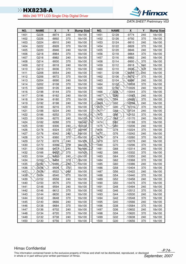
-P.74- This information contained herein is the exclusive property of Himax and shell not be distributed, reproduced, or disclosed in whole or in part without prior written permission of Himax.
Himax Confidential
September, 2007
HX8238-A 960x 240 TFT LCD Single Chip Digital Driver
DATA SHEET Preliminary V03
NO. NAME X Y Bump Size NO. NAME X Y Bump Size
1401 G228 -8874 240 18x100 1451 G128 -9774 240 18x100
1402 G226 -8892 370 18x100 1452 G126 -9792 370 18x100
1403 G224 -8910 240 18x100 1453 G124 -9810 240 18x100
1404 G222 -8928 370 18x100 1454 G122 -9828 370 18x100
1405 G220 -8946 240 18x100 1455 G120 -9846 240 18x100
1406 G218 -8964 370 18x100 1456 G118 -9864 370 18x100
1407 G216 -8982 240 18x100 1457 G116 -9882 240 18x100
1408 G214 -9000 370 18x100 1458 G114 -9900 370 18x100
1409 G212 -9018 240 18x100 1459 G112 -9918 240 18x100
1410 G210 -9036 370 18x100 1460 G110 -9936 370 18x100
1411 G208 -9054 240 18x100 1461 G108 -9954 240 18x100
1412 G206 -9072 370 18x100 1462 G106 -9972 370 18x100
1413 G204 -9090 240 18x100 1463 G104 -9990 240 18x100
1414 G202 -9108 370 18x100 1464 G102 -10008 370 18x100
1415 G200 -9126 240 18x100 1465 G100 -10026 240 18x100
1416 G198 -9144 370 18x100 1466 G98 -10044 370 18x100
1417 G196 -9162 240 18x100 1467 G96 -10062 240 18x100
1418 G194 -9180 370 18x100 1468 G94 -10080 370 18x100
1419 G192 -9198 240 18x100 1469 G92 -10098 240 18x100
1420 G190 -9216 370 18x100 1470 G90 -10116 370 18x100
1421 G188 -9234 240 18x100 1471 G88 -10134 240 18x100
1422 G186 -9252 370 18x100 1472 G86 -10152 370 18x100
1423 G184 -9270 240 18x100 1473 G84 -10170 240 18x100
1424 G182 -9288 370 18x100 1474 G82 -10188 370 18x100
1425 G180 -9306 240 18x100 1475 G80 -10206 240 18x100
1426 G178 -9324 370 18x100 1476 G78 -10224 370 18x100
1427 G176 -9342 240 18x100 1477 G76 -10242 240 18x100
1428 G174 -9360 370 18x100 1478 G74 -10260 370 18x100
1429 G172 -9378 240 18x100 1479 G72 -10278 240 18x100
1430 G170 -9396 370 18x100 1480 G70 -10296 370 18x100
1431 G168 -9414 240 18x100 1481 G68 -10314 240 18x100
1432 G166 -9432 370 18x100 1482 G66 -10332 370 18x100
1433 G164 -9450 240 18x100 1483 G64 -10350 240 18x100
1434 G162 -9468 370 18x100 1484 G62 -10368 370 18x100
1435 G160 -9486 240 18x100 1485 G60 -10386 240 18x100
1436 G158 -9504 370 18x100 1486 G58 -10404 370 18x100
1437 G156 -9522 240 18x100 1487 G56 -10422 240 18x100
1438 G154 -9540 370 18x100 1488 G54 -10440 370 18x100
1439 G152 -9558 240 18x100 1489 G52 -10458 240 18x100
1440 G150 -9576 370 18x100 1490 G50 -10476 370 18x100
1441 G148 -9594 240 18x100 1491 G48 -10494 240 18x100
1442 G146 -9612 370 18x100 1492 G46 -10512 370 18x100
1443 G144 -9630 240 18x100 1493 G44 -10530 240 18x100
1444 G142 -9648 370 18x100 1494 G42 -10548 370 18x100
1445 G140 -9666 240 18x100 1495 G40 -10566 240 18x100
1446 G138 -9684 370 18x100 1496 G38 -10584 370 18x100
1447 G136 -9702 240 18x100 1497 G36 -10602 240 18x100
1448 G134 -9720 370 18x100 1498 G34 -10620 370 18x100
1449 G132 -9738 240 18x100 1499 G32 -10638 240 18x100
1450 G130 -9756 370 18x100 1500 G30 -10656 370 18x100

-P.75- This information contained herein is the exclusive property of Himax and shell not be distributed, reproduced, or disclosed in whole or in part without prior written permission of Himax.
Himax Confidential
September, 2007
HX8238-A 960x 240 TFT LCD Single Chip Digital Driver
DATA SHEET Preliminary V03
NO. NAME X Y Bump Size
1501 G28 -10674 240 18x100
1502 G26 -10692 370 18x100
1503 G24 -10710 240 18x100
1504 G22 -10728 370 18x100
1505 G20 -10746 240 18x100
1506 G18 -10764 370 18x100
1507 G16 -10782 240 18x100
1508 G14 -10800 370 18x100
1509 G12 -10818 240 18x100
1510 G10 -10836 370 18x100
1511 G8 -10854 240 18x100
1512 G6 -10872 370 18x100
1513 G4 -10890 240 18x100
1514 G2 -10908 370 18x100
1515 G0 -10926 240 18x100
1516 DUMMY -10944 370 18x100
1517 DUMMY -10962 240 18x100
1518 THROUGH7 -10980 370 18x100
1519 THROUGH8 -10998 240 18x100
1520 DUMMY -11016 370 18x100
1521 L_MARK -10967.5 -145 NA

-P.76- This information contained herein is the exclusive property of Himax and shell not be distributed, reproduced, or disclosed in whole or in part without prior written permission of Himax.
Himax Confidential
September, 2007
HX8238-A 960x 240 TFT LCD Single Chip Digital Driver
DATA SHEET Preliminary V03
17. Ordering Information
Part NO. Package
HX8238-A00BPDXXX PD: means COG XXX: means chip thickness(µm), default 400µm For CMO 3.5G panel (Panel name: F3506)
HX8238-A02BPDXXX PD: means COG XXX: means chip thickness(µm), default 400µm For CMO 4G panel (Panel name: F3507)

-P.77- This information contained herein is the exclusive property of Himax and shell not be distributed, reproduced, or disclosed in whole or in part without prior written permission of Himax.
Himax Confidential
September, 2007
HX8238-A 960x 240 TFT LCD Single Chip Digital Driver
DATA SHEET Preliminary V03
18. Revision History
Version Date Description of Changes 2006/07/21 New setup
2006/08/03 1.Change display color to 262K 2.Add register R04h and R05h
2006/08/16 1. Add POL and QXH pin
2006/09/08 1.Add PWM function 2.Add Pin Sequence
2006/09/18 1.Modify pin sequence 2.Add pin SEL[2:0] and SWD[2:0]
2006/10/11 1.Add CPE pin 2.Add PINV/LPF bits 3.Modify TB pin definition
2006/10/23 1.Add R0Ah 2.Add GDIS/XDK/GHN bit in R05h 3.Modify pin description for some pull high/low pins 4.Modify gamma table
2006/10/25 1.Add VDS bit in R0Dh, FB bit in R05h and PALM bit in R04h
2.Update OTP write sequence 3.Add PINV pin 4.Add aging mode 5.Modify data setup/hold time
00
2006/11/21 1.Modify the SPI default values. (page 13) 2. Add CCIR601/656 timing. (page 43~46)
2006/11/30 1.Add pad location and bump information 2.SWAP C3P/C3N, C2P/C2N, CP/CN,
CXP/CXN/CYP/CYN pin sequence 3.Change VDD voltage spec. to 1.8V~2.5V 4.Add VRC[2:0] bit in R0Dh 5.Modify SPI default value
01
2007/01/25 1.Modify TEST 4~5 pin definition 2.Modify Figure 4.1 3.Modify Figure 16.2 4.Modify Figure 16.3 5.Modify Figure 16.5 6.Modify Table 9.3 7.Modify Table 9.12 8.Modify Table 14.2
02 2007/03/21 1.Modify Table 8.1 Command table 2. Modify Figure 9. 3 Driver Output Control 3. Modify Table 9. 1 Source output level 4. Modify Figure 14. 10 Power up sequence 5.Modify Table 14.3 Power up sequence 6. Modify Figure 14. 11 Power down sequence 7.Remove VCOMG function on R0Eh 8.Change the description of CPE on pin description 9.Change the description of CPE on R01h 10.Change the description of DCT3-0 and DC3-0 on R03h 11.Add the description of GDIS on R05h 12. Modify Figure 16. 4 Panel and FPC connection 13. Change Part NO. to HX8238-A00BPD400

-P.78- This information contained herein is the exclusive property of Himax and shell not be distributed, reproduced, or disclosed in whole or in part without prior written permission of Himax.
Himax Confidential
September, 2007
HX8238-A 960x 240 TFT LCD Single Chip Digital Driver
DATA SHEET Preliminary V03
2007/04/11 1. Modify Table 10. 8 OTP Programming Sequence 2. Modify Figure 10. 5 OTP Programming Circuitry
2007/05/24 1. Modify Table 9. 3VGH and VGL Booster Ratio 2. Modify Table 13. 1 DC Characteristics 3.Change VDDIO spec 4. Add Figure 14. 12(b) 5. Modify Figure 16. 6 Booster Capacitors 6. Modify Figure 16. 3 Filtering and Charge Sharing
Capacitors
02
2007/06/25 1. Add Figure 14. 3(a) Data Transaction Timing in Serial RGB (8 bit) Interface (SYNC Mode)
2. Add Figure 14. 3(b) Data Transaction Timing in Serial RGB (8 bit) Interface (DE Mode)
2007/06/26 1.Modify OTP Programming from two times to one time
2007/07/24 1.Modify Figure 8.3 Gamma Control 1
2007/08/28 1. Modify Table 12. 1 DC Characteristics 2. Modify Table 13. 3 Power Up Sequence 3. Modify Table 13. 4 Power Down Sequence 4. Modify Table 13. 5 SPI Timing 5. Modify Figure 13. 1 Pixel Timing 6. Modify Figure 13. 11 Power Up Sequence 7. Modify Figure 13. 12 Power Down Sequence 8. Add Table 6. 1R/S & R/W setting 9. Add Figure13. 15 Rising/Falling time 10.Add the description of SPI on page 13
03
2007/09/03 1. Modify OTP default value
Related Documents


![Himax Investor Presentation 2013 Aug Final [相容模式] · 2018-08-28 · Himax Oppg perating Companies Hi T h l i Ltd Himax Media Solutions Inc zDisplay Drivers and Tcon zTouch](https://static.cupdf.com/doc/110x72/5f79ab6a890821335e355f58/himax-investor-presentation-2013-aug-final-c-2018-08-28-himax-oppg.jpg)