IEICE TRANS. ELECTRON., VOL.E103–C, NO.11 NOVEMBER 2020 619 INVITED PAPER Special Section on Opto-electronics and Communications for Future Optical Network High-Speed-Operation of All-Silicon Lumped-Electrode Modulator Integrated with Passive Equalizer Yohei SOBU † a) , Shinsuke TANAKA † , and Yu TANAKA † , Members SUMMARY Silicon photonics technology is a promising candidate for small form factor transceivers that can be used in data-center applications. This technology has a small footprint, a low fabrication cost, and good temperature immunity. However, its main challenge is due to the high baud rate operation for optical modulators with a low power consumption. This paper investigates an all-Silicon Mach-Zehnder modulator based on the lumped-electrode optical phase shifters. These phase shifters are driven by a complementary metal oxide semiconductor (CMOS) inverter driver to achieve a low power optical transmitter. This architecture improves the power efficiency because an electrical digital-to-analog converter (DAC) and a linear driver are not required. In addition, the current only flows at the time of data transition. For this purpose, we use a PIN-diode phase shifter. These phase shifters have a large capacitance so the driving volt- age can be reduced while maintaining an optical phase shift. On the other hand, this study integrates a passive resistance-capacitance (RC) equalizer with a PIN-phase shifter to expand the electro-optic (EO) bandwidth of a modulator. Therefore, the modulation efficiency and the EO bandwidth can be optimized by designing the capacitor of the RC equalizer. This paper re- views the recent progress for the high-speed operation of an all-Si PIN-RC modulator. This study introduces a metal-insulator-metal (MIM) structure for a capacitor with a passive RC equalizer to obtain a wider EO bandwidth. As a result, this investigation achieves an EO bandwidth of 35.7–37 GHz and a 70 Gbaud NRZ operation is confirmed. key words: photonic integrated circuit, silicon photonics, optical modula- tor, passive equalizer 1. Introduction A rapid increase of the global data traffic in an optical network represents the Compound Annual Growth Rate (CAGR) over 25% for both intensity-modulation direct- detection (IM-DD) and coherent detection scheme in the Global Cloud Index (GCI) report [1]. Due to the strong de- mands from the optical network application (e.g. data cen- ters), a large transmission capacity and a low power con- sumption are necessary for compact transceivers such as Quad Small Form-factor Pluggable Double Density (QSFP- DD) or Octal Small Form-factor Pluggable (OSFP) mod- ules [2]. Silicon (Si) photonics is one of the most promis- ing platforms for these applications. They can achieve a highly dense photonics integrated circuit (PIC) due to its high index contrast with the Si/SiO 2 waveguide. To date, some Si PICs have successfully demonstrated their large- capacity and highly-dense data transmission [3], [4]. A fur- ther increase in the transmission bandwidth is required for Manuscript received December 27, 2019. Manuscript revised April 16, 2020. Manuscript publicized May 15, 2020. † The authors are with Fujitsu Limited, Kawasaki-Shi, 212– 8510 Japan. a) E-mail: [email protected] DOI: 10.1587/transele.2019OCP0006 the next-generation standard of 400 Gbps and beyond while maintaining a low cost and a low power consumption. How- ever, the main challenge remains with a higher baud rate operation with a low power consumption for the optical modulator. To date, several types of Si modulators have been de- veloped for high-speed modulation, high modulation effi- ciency, and low power consumption [5]. When considering the coherent transmission, the Mach-Zehnder-type modula- tor (MZM) is suitable in terms of the required range for an operating wavelength and the modulation scheme. The cur- rent trend in the development of a Si modulator is for a wide bandwidth demonstration by introducing heterogeneous in- tegration with other materials. A Si-organic hybrid modula- tor and a plasmonic modulator are promising candidates for the next-generation high-speed optical modulators beyond the 100 Gbaud in the Si photonics platform [6]–[8]. These modulators have not demonstrated their usability in terms of the foundry process compatibility for mass production and long-term reliability. In contrast, all-Si-based optical mod- ulators are attractive candidates because of their compati- bility in the foundry process, their highly dense assembly with an electrical driver, high reliability, and small tempera- ture dependency [9]. However, all-Si modulators have some concerns in order to achieve high performance. The carrier plasma effect that is used in all-Si modulators has a rela- tively weak effect for the refractive index change. They also have a trade-off between the operation bandwidth and the modulation efficiency. This can be attributed to the capaci- tance of the phase shifter, which is linked to the modulation efficiency. Therefore, high-speed all-Si modulators have been developed while addressing these concerns. In partic- ular, high-speed traveling-wave (TW) type modulators have PN depletion mode that have been investigated [5], [10]. They are mostly driven with an electrical digital-to-analog converter (DAC) and a large-swing linear driver. However, as the symbol rate of the system increases, it is difficult to maintain a large swing due to the trade-off relationship between the modulation depth and the power consumption. Therefore, the current trend of high-speed all-Si modulators are to compensate the high-speed modulators by a strong digital signal processing (DSP) equalizer. Although an 80 Gbaud PAM8 and an 80 Gbaud to 100 Gbaud QAM oper- ation have been demonstrated with offline DSP technology, there is a concern about the power consumption [11]–[14]. From these backgrounds, a new approach for the Si pho- tonics modulator to obtain a high-speed modulation and a Copyright c 2020 The Institute of Electronics, Information and Communication Engineers

Welcome message from author
This document is posted to help you gain knowledge. Please leave a comment to let me know what you think about it! Share it to your friends and learn new things together.
Transcript

IEICE TRANS. ELECTRON., VOL.E103–C, NO.11 NOVEMBER 2020619
INVITED PAPER Special Section on Opto-electronics and Communications for Future Optical Network
High-Speed-Operation of All-Silicon Lumped-Electrode ModulatorIntegrated with Passive Equalizer
Yohei SOBU†a), Shinsuke TANAKA†, and Yu TANAKA†, Members
SUMMARY Silicon photonics technology is a promising candidate forsmall form factor transceivers that can be used in data-center applications.This technology has a small footprint, a low fabrication cost, and goodtemperature immunity. However, its main challenge is due to the highbaud rate operation for optical modulators with a low power consumption.This paper investigates an all-Silicon Mach-Zehnder modulator based onthe lumped-electrode optical phase shifters. These phase shifters are drivenby a complementary metal oxide semiconductor (CMOS) inverter driverto achieve a low power optical transmitter. This architecture improves thepower efficiency because an electrical digital-to-analog converter (DAC)and a linear driver are not required. In addition, the current only flows atthe time of data transition. For this purpose, we use a PIN-diode phaseshifter. These phase shifters have a large capacitance so the driving volt-age can be reduced while maintaining an optical phase shift. On the otherhand, this study integrates a passive resistance-capacitance (RC) equalizerwith a PIN-phase shifter to expand the electro-optic (EO) bandwidth of amodulator. Therefore, the modulation efficiency and the EO bandwidth canbe optimized by designing the capacitor of the RC equalizer. This paper re-views the recent progress for the high-speed operation of an all-Si PIN-RCmodulator. This study introduces a metal-insulator-metal (MIM) structurefor a capacitor with a passive RC equalizer to obtain a wider EO bandwidth.As a result, this investigation achieves an EO bandwidth of 35.7–37 GHzand a 70 Gbaud NRZ operation is confirmed.key words: photonic integrated circuit, silicon photonics, optical modula-tor, passive equalizer
1. Introduction
A rapid increase of the global data traffic in an opticalnetwork represents the Compound Annual Growth Rate(CAGR) over 25% for both intensity-modulation direct-detection (IM-DD) and coherent detection scheme in theGlobal Cloud Index (GCI) report [1]. Due to the strong de-mands from the optical network application (e.g. data cen-ters), a large transmission capacity and a low power con-sumption are necessary for compact transceivers such asQuad Small Form-factor Pluggable Double Density (QSFP-DD) or Octal Small Form-factor Pluggable (OSFP) mod-ules [2]. Silicon (Si) photonics is one of the most promis-ing platforms for these applications. They can achieve ahighly dense photonics integrated circuit (PIC) due to itshigh index contrast with the Si/SiO2 waveguide. To date,some Si PICs have successfully demonstrated their large-capacity and highly-dense data transmission [3], [4]. A fur-ther increase in the transmission bandwidth is required for
Manuscript received December 27, 2019.Manuscript revised April 16, 2020.Manuscript publicized May 15, 2020.†The authors are with Fujitsu Limited, Kawasaki-Shi, 212–
8510 Japan.a) E-mail: [email protected]
DOI: 10.1587/transele.2019OCP0006
the next-generation standard of 400 Gbps and beyond whilemaintaining a low cost and a low power consumption. How-ever, the main challenge remains with a higher baud rateoperation with a low power consumption for the opticalmodulator.
To date, several types of Si modulators have been de-veloped for high-speed modulation, high modulation effi-ciency, and low power consumption [5]. When consideringthe coherent transmission, the Mach-Zehnder-type modula-tor (MZM) is suitable in terms of the required range for anoperating wavelength and the modulation scheme. The cur-rent trend in the development of a Si modulator is for a widebandwidth demonstration by introducing heterogeneous in-tegration with other materials. A Si-organic hybrid modula-tor and a plasmonic modulator are promising candidates forthe next-generation high-speed optical modulators beyondthe 100 Gbaud in the Si photonics platform [6]–[8]. Thesemodulators have not demonstrated their usability in terms ofthe foundry process compatibility for mass production andlong-term reliability. In contrast, all-Si-based optical mod-ulators are attractive candidates because of their compati-bility in the foundry process, their highly dense assemblywith an electrical driver, high reliability, and small tempera-ture dependency [9]. However, all-Si modulators have someconcerns in order to achieve high performance. The carrierplasma effect that is used in all-Si modulators has a rela-tively weak effect for the refractive index change. They alsohave a trade-off between the operation bandwidth and themodulation efficiency. This can be attributed to the capaci-tance of the phase shifter, which is linked to the modulationefficiency. Therefore, high-speed all-Si modulators havebeen developed while addressing these concerns. In partic-ular, high-speed traveling-wave (TW) type modulators havePN depletion mode that have been investigated [5], [10].They are mostly driven with an electrical digital-to-analogconverter (DAC) and a large-swing linear driver. However,as the symbol rate of the system increases, it is difficultto maintain a large swing due to the trade-off relationshipbetween the modulation depth and the power consumption.Therefore, the current trend of high-speed all-Si modulatorsare to compensate the high-speed modulators by a strongdigital signal processing (DSP) equalizer. Although an 80Gbaud PAM8 and an 80 Gbaud to 100 Gbaud QAM oper-ation have been demonstrated with offline DSP technology,there is a concern about the power consumption [11]–[14].From these backgrounds, a new approach for the Si pho-tonics modulator to obtain a high-speed modulation and a
Copyright c© 2020 The Institute of Electronics, Information and Communication Engineers

620IEICE TRANS. ELECTRON., VOL.E103–C, NO.11 NOVEMBER 2020
low power consumption is the optical time division multi-plexing scheme [15], [16]. They use a mode locked laser,an optical serializer, and limited (quarter rate) electronicsto achieve a 104 Gbaud operation, or a 1.5pJ/bit. How-ever, they have an additional loss of 6 dB due to the opticalserializer.
From this overview, Si modulators have not beendemonstrated for high-speed multi-level operations and alow power consumption for the same device under the sameconditions [17]. To reduce power consumption, it is effec-tive to combine an efficient lumped-electrode phase shifterand a CMOS inverter driver. However, it cannot supportmulti-level modulation format, as this architecture is limitedto a binary operation. Then, an optical DAC architecture is agood solution. The binary signals are multiplexed at the op-tical domain by using a segmented modulator [18], [19]. Infact, a low power operation in higher-order modulation sig-nals such as pulse amplitude modulation (PAM) and quadra-ture amplitude modulation (QAM) has been demonstratedby using optical DAC technology [20]–[23]. For this archi-tecture, an electrical DAC and a large swing linear driverare not required. To achieve this architecture more effec-tively, this study introduces a forward-biased PIN phaseshifter that is integrated with a passive RC equalizer (PIN-RC). In our previous study, we reported a very low VπL of0.31 Vcm for a 25 Gbps modulator [24]. This concept canoptimize the trade-off between the electro-optic (EO) band-width and the modulation efficiency since the capacitanceof PIN-RC modulator can be controlled. Then, we demon-strated a very-low-power operation (1.59 mW/Gbps) of a56-Gbps PAM4 oDAC transmitter by combining the CMOSinverter driver and the segmented modulator [23]. However,the modulation speed was limited by the RC constant of theoptical phase shifter. We also demonstrated the feasibil-ity of high-speed modulation by using a lumped electrodePIN-RC modulator, which improves the design of the all-Si PIN-RC phase shifters [25]. This investigation reviewsthe design controllability and the measurement results of thePIN-RC modulator by introducing a metal-insulator-metal(MIM) structure into the capacitor of a passive RC equal-izer. This is achieved with a 3-dB bandwidth (f3dB) of 35.7–37 GHz. This confirms the 70 Gbaud NRZ operation with aclear optical eye opening.
The rest of this paper is organized as follows. Section 2describes the design of the PIN-RC modulator by using anequivalent circuit of the PIN phase shifter and the RC equal-izer. The parameters of the PIN-RC modulator for the high-speed-operation are listed in this section. The fabricationand the measurement results of the PIN-RC modulator areverified in Sect. 3. The results of the DC characteristics, theelectro-optic (EO) response, and the high-speed-large signaltest are also mentioned. Section 4 discusses the estimatedperformances when applying the CMOS inverter driver (i.e.,removing the limitation of the 50Ω systems). Finally, a briefsummery is provided in Sect. 5.
2. Design and Fabrication of the PIN-RC Modulator
2.1 Lumped Electrode PIN Phase Shifter
This section describes the design and parameters of thelumped electrode PIN-RC modulator. Generally, the freecarrier plasma effect is widely used in silicon photonicsmodulators since the EO effect is small for the silicon phaseshifter [5]. The Si phase shifter generates an optical phaseshift that corresponds to the amount of the electric chargedepleted or injected by the driver circuit. The Si phaseshifters, such as the PN and PIN diodes, are commonly usedbecause they are compatible with the foundry process anda small dependence of operating wavelength and tempera-ture. The fundamental efficiency of the Si phase shifter isdetermined by the overlap of the electrical carrier distribu-tion and the optical field in Si waveguide. In the case ofthe commonly used Si phase shifter, an electric charge is re-quired to give an optical phase shift equal to π (Qπ), which isapproximately 3∼6 pC [24], [26]. To achieve a higher powerefficiency in this type of situation, the following two view-points should be considered.
First, the driving architecture needs to be considered soit supplies an electric charge into the optical phase shifter ef-ficiently. Currently, the traveling-wave (TW) type Si phaseshifter with a differential radio frequency (RF) transmissionline is commonly used. However, in this architecture, thecurrent is supplied constantly to the differential RF trans-mission line by the current mode logic (CML) driver. As aresult, the power efficiency is low. Afterwards, impedancematching between the CML driver and the optical phaseshifter is required. On the other hand, the Si phase shiftercan be divided into a short segment and can be treated as alumped electrode driven by a CMOS inverter driver. In thiscase, as the current is supplied through data transition, thepower efficiency is very high. Also, the lumped electrodearchitecture enables an easy design of the EO bandwidth.
Second, the types of phase shifters should be properlyselected. To obtain a high power efficiency in the case of thelumped electrode architecture, the phase shifter with a largecapacitance needs to be applied. Additionally, it is desir-able to fabricate the phase shifter with the standard foundryprocess.
Therefore, for this study, the lumped-electrodeforward-biased PIN phase shifter with a large capacitancewas chosen. The PIN phase shifter is composed of anun-doped intrinsic layer inside the Si core layer within480 nm × 220 nm waveguides and p- and n-Si conductinglayers on a Si slab layer as shown in Fig. 1. An EO band-width of the lumped electrode optical modulators is limitedby the RC constant of the phase shifters. Figure 2 illustratesthe equivalent circuit of the PIN phase shifter. This consistsof a parallel arranged capacitance and resistance (CF and RF)for the PIN diode and the series resistance (RS). The lengthof the phase shifter to be 250 μm, and the CF, RF, and RS
are 13.2 pF, 197 Ω, and 12.2 Ω, respectively. This study

SOBU et al.: HIGH-SPEED-OPERATION OF ALL-SILICON LUMPED-ELECTRODE MODULATOR INTEGRATED WITH PASSIVE EQUALIZER621
Fig. 1 Cross sectional view of PIN phase shifter.
Fig. 2 Equivalent circuit model of PIN phase shifter and driver.
assumes that the driver impedance is 50 Ω when consider-ing the measurement setup of the Si photonics chip. In thiscase, the EO bandwidth (f3dB) is calculated by the followingequation.
f3dB = 1/2π(RS + Rdrv)CF (1)
The EO bandwidth of the PIN phase shifter is limited toseveral hundred MHz mainly due to the large capacitanceCF of the intrinsic region.
2.2 PIN Phase Shifter Integrated with RC Equalizer
To extend the EO bandwidth of the entire system for high-speed operation, this study introduced a passive equalizationtechnique that inserts a simple RC filter between the driverand the PIN phase shifter as presented in the left equivalentcircuit in Fig. 3 [23]–[25]. The capacitance CE and the resis-tance RE can be satisfied with the following equation.
CE = CF/η, RE = RF × η, η � 1 (2)
From this, the capacitance CE enhances the EO bandwidthby reducing the effective capacitance of the PIN phaseshifter by applying Eq. (3).
(1/CE + 1/CF)−1 ∼ CE = CF/η (3)
In addition, a resistance RE for the equalizer is inserted toobtain a flat EO response over the entire signal frequency.
Fig. 3 Equivalent circuit model of PIN phase shifter that is integratedwith passive RC equalizer.
Fig. 4 Calculated optical responses of PIN phase shifter (black line) andPIN phase shifter with passive RC equalizer (red line).
As a result, the equivalent circuit become a simple RC cir-cuit in the right side of Fig. 3. This means that the EO band-width of the entire system is extended by a factor of η. In thistime, η, CE, and RE is set to be 205, 64.4 fF, and 40.5 kΩ,respectively, to achieve 3dB EO bandwidth of 40 GHz, byusing Eqs. (2) and (4).
f3dB = 1/2π(RS + Rdrv)CE (4)
Figure 4 displays the calculated small-signal EO responsesof the entire system. The black and red line show the EOresponses with the un-equalized and equalized PIN phaseshifter. The un-equalized PIN-PS exhibits too large of anEO response (∝ 20 log(1/Vπ)) at a low frequency regime.The RC filter de-emphasis the excess EO response by a fac-tor of 1/η2. As a result, the EO response of the equalizedPIN phase shifter exhibits a flat response up to the designedEO bandwidth of 40 GHz. In this scheme, the relationship

622IEICE TRANS. ELECTRON., VOL.E103–C, NO.11 NOVEMBER 2020
Fig. 5 Cross-sectional view of Si-MZM involving PIN phase shifter thatis integrated with RC equalizer.
of the trade-off between the required EO bandwidth and themodulation efficiency can be optimized by designing theRC equalizer. This equalization technique requires no ad-ditional power because it consists of only a passive compo-nent. The EO response of this system is also strongly af-fected by the driver impedance Rdrv. Therefore, in the caseof using the CMOS inverter driver with Rdrv of several Ω,the expansion of the EO response or the improvement of thepower efficiency can be achieved. Namely, the lumped elec-trode PIN-RC modulator is suitable with a high-speed and ahigh-power efficiency modulation.
In this design scheme, the high accuracy and the con-trollability of the capacitance CE and the suppression ofthe parasitic capacitance are important to enable the stablebroadband operation of the modulator. Therefore, this in-vestigation introduced the metal insulator metal (MIM) ca-pacitor to precisely define the CE. The thinner the insulationlayer is between the metal layers, the greater the reductionof the area of the MIM structure. As a result, a smaller par-asitic capacitance can be obtained. In addition, a thinnerinsulation layer enables the precise control of the CE. Fig-ure 5 depicts the cross-sectional view of the PIN-RC modu-lator. The resistance of the RC equalizer was fabricated bythe n-type Si doped layer.
2.3 Design Parameters of PIN-RC Modulator
This section discusses the design parameters of the PIN-RCmodulator. Two types of modulators were fabricated withthe EO bandwidth of 30 GHz (design (a)) and 40 GHz (de-sign (b)). The length of the PIN phase shifter was 250 μm.The parameters of the passive RC equalizer were optimizedto obtain the required EO bandwidth of the modular as dis-played in Table 1.
2.4 Fabricated PIN-RC Modulator
The PIN-RC modulators were fabricated by using a stan-dard Si photonics process at a commercial CMOS foundry.An example of the fabricated device is featured in Fig. 6. Ithas an asymmetric Si MZM. The device has GSG pads fordifferential driving. The passive RC equalizer had a very
Table 1 Design parameters and values of PIN RC modulator. Design (a)and design (b) are for EO bandwidth of 30 GHz and 40 GHz respectively.
Fig. 6 Fabricated device of Si-PIN-MZM.
compact footprint of < 50 x 60 μm2 and it can be placednear the PIN phase shifters. The total footprint of the fabri-cated modulator was only < 400 x 500 μm2, which includesthe GSG probe pads. Thus, these structures are suitable forfuture optical DAC architecture designs. This is becausethe densely segmented MZM layout can be combined byemploying U-shaped-phase shifters and highly dense metalpads for flipchip bonding.
3. Measurement Results of PIN-RC Modulator
3.1 Experiment Setup
Figure 7 illustrates the experimental setup of the DC char-acteristics, the EO response, and the high-speed large sig-nal operation. The black and red lines correspond to theelectrical cable and the optical single mode fiber, respec-tively. First, this investigation confirmed the IV character-istics of the PIN-diode with the passive RC equalizer. Sec-ond, the modulation efficiency (VπL) was calculated by us-ing the measured bias voltage dependence of the opticalinterference spectrum shift from the optical spectrum an-alyzer (YOKOGAWA, AQ6370). Third, the EO responseof the PIN-RC modulator was measured with a lightwave

SOBU et al.: HIGH-SPEED-OPERATION OF ALL-SILICON LUMPED-ELECTRODE MODULATOR INTEGRATED WITH PASSIVE EQUALIZER623
Fig. 7 Measurement setup of IV characteristics, modulation efficiency,EO response, and high-speed large signal test.
component analyzer (LCA) (Keysight, N4373D). For thisstudy, the EO bandwidth was measured to confirm the con-sistency between the design value of the capacitance (CE) ofthe RC equalizer and the measurement results.
Finally, the high-speed large signal test was measured.The details of this test are mentioned in Sect. 3.3. The mea-surement conditions are in the C-band at room temperature.
3.2 Measured Results of DC Characteristics and EOResponse
This section discusses the measurement results of the I-Vcharacteristics, VπL, and the EO response of the PIN-RCmodulator. As described in the design section, this studycompared the measured results between the two types of de-signs. The I-V characteristics exhibited the forward-biaseddiode response with a resistance RE as shown in Fig. 8. Theresistance RE was measured to be 27.1 kΩ and 36.1 kΩfor design (a) and design (b) respectively. The bias current(Ibias) was measured to be 0.145 and 0.193 mA at a forwardbias voltage of 6V. Then, the partial bias on PIN-diode canbe calculated by subtracting the voltage drop at the resis-tance RE from 6V. Each partial bias on PIN-diode was 0.75and 0.77 V in design (a) and design (b) respectively. Fig-ure 9 corresponds to the forward bias dependencies of VπL,which is calculated by the optical phase shift for both de-signs with both arms respectively. An optical phase shift isderived from the transmission spectrum shift, which followsthe applied DC bias voltage. The VπL was obtained to beapproximately 1.7 Vcm and 2 Vcm at a forward bias voltageof 6 V. From these results, the π-phase shift charge (Qπ) can
Fig. 8 Measured IV characteristics for design (a) and design (b)
Fig. 9 Measured VπL for design (a) and design (b)
Fig. 10 Measured EO response for design (a) and design (b)
be calculated to be 5.1∼5.8 pC which is almost common forvarious types of Si PS [24], [26]. The optical propagationloss of the phase shifter was measured to be 27.8 dB/cm,which corresponds to a modulator insertion loss of 0.7 dB.
Figure 10 demonstrates the measured small-signal EOresponses for both designs with both arms of the fabricatedmodulator with forward bias of 6V, respectively. The EO re-sponses were normalized in the low frequency range. This

624IEICE TRANS. ELECTRON., VOL.E103–C, NO.11 NOVEMBER 2020
Table 2 Measured values of EO bandwidth and modulation efficiency ofPIN-RC modulators for design (a) and design (b).
study obtained wide and flat EO responses because of theoptimized RC equalizer setting. The f3dB was measured tobe 27.5-29 GHz for design (a) and 35.7–37 GHz for design(b), respectively. The measured values of the VπL and f3dB
were summarized in Table 2. The measured characteristicswere almost consistent with the design value. Design (a) hasa higher modulation efficiency and a smaller EO bandwidthbecause it has a larger capacitance, CE. From these measure-ment results, the optimization of the trade-off between themodulation efficiency and the expanded EO bandwidth ofthe PIN-RC modulator was successfully demonstrated withgood controllability by introducing MIM-type capacitor intothe RC passive equalizer.
3.3 Measured Characteristics of High-Speed Large SignalOperation
This section begins by discussing the experimental setupand the conditions for the measurement. For the large signalmeasurement, this investigation used an arbitrary waveformgenerator (AWG, Keysight, M8196A), RF phase matchingcables, RF amplifiers (SHF, L810), bias-tees, and RF probes(Form Factor, Infinity probe) in a push-pull manner. The to-tal frequency response of these RF components except forthe RF probes was compensated by the AWG. The modula-tor was driven with a pseudorandom binary sequence NRZsignal of 211 − 1 generated from the AWG with a raised co-sine filter of α = 0.1∼0.5. The baud rate of the NRZ sig-nal was varied from 40 Gbaud to 70 Gbaud. The peak-to-peak amplitude (Vpps) in the drive signal was measured tobe 2.3–4.8 V for each modulation speed shown. The val-ues of Vpps decreased with the increased baud rate becauseof the influence of the limited bandwidth and nonlinearity ofthe AWG and RF amplifier. The input wavelength was set tothe quadrature point while using the asymmetric MZI. In theexperiment, the bias voltage was fixed at 6 V to maintain thesame bias condition for the small-signal measurement. Themeasured device in design (b) demonstrates the high-speedlarge signal operation. The modulated signal was amplifiedby an Erbium Doped Fiber Amplifier (EDFA) and recordedwith a sampling oscilloscope (Keysight, 86100D) that hasan optical plugin module with a bandwidth of 65 GHz. Theinput electrical waveform and the output optical waveformsfor 40 Gbaud to 70 Gbaud NRZ operations are describedin Table 3. The measured Vpps and the extinction ration(ER) of the measured optical waveform were also summa-rized. The clear eye opening for each data rate was con-firmed. The measured extinction ratio (ER) was 3.4 dB at40 Gbaud, 3.2 dB at 50 Gbaud, 2.4 dB at 60 Gbaud, and
Table 3 40-70 Gbaud electrical input waveform with peak-to-peak am-plitude in NRZ drive signal and measured optical eye diagram. This in-cludes extinction ratio of PIN-RC modulator in case of design (b).
1.6 dB at 70 Gbaud. For each modulation speed, this inves-tigation observed that the optical waveforms were similarto the electrical eye waveforms of the drive signal. Thisfinding indicates that the large-signal bandwidth was notmainly limited by the bandwidth of the Si modulator forthese operation speeds. Therefore, high-speed operationsover 70 Gbaud can be achieved by the optimization of themeasurement setup of the RF signals.
4. Discussion
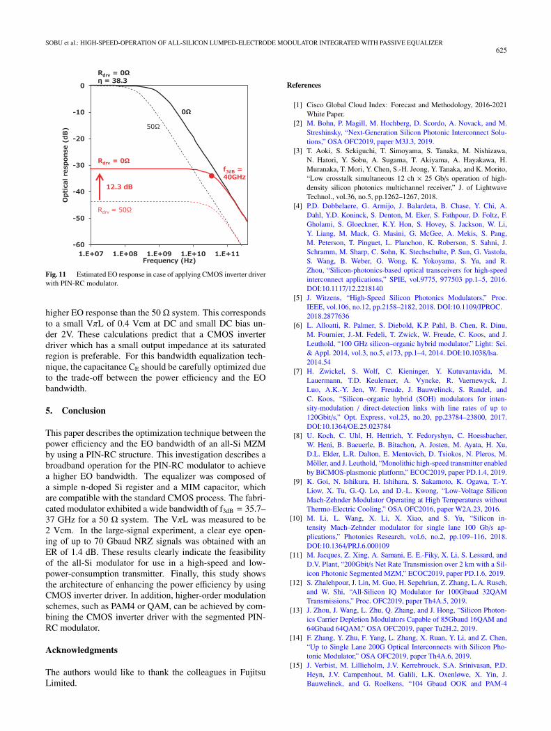
Overall, this investigation demonstrates the feasibility of thehigh-speed operation of an all-Si PIN-RC MZM. In thisstudy, the modulation efficiency was limited to a small valueof VπL (2 Vcm) because the EO response and modula-tion efficiency are affected by the limitation of the outputimpedance of the driver (Rdrv = 50Ω). In the case where theCMOS inverter driver is combined with the PIN-RC mod-ulator [23], this can significantly enhance the modulationefficiency because of the small output impedance (severalΩ) for the CMOS inverters. Figure 11 corresponds to theestimated EO response when applying the CMOS inverterdriver. The dashed line shows the optical response of Rdrv at50 Ω which is the same as demonstrated in Fig. 4. The boldline shows the case of Rdrv at 0 Ω. In the case of Rdrv = 0,we can improve the modulation efficiency (CE) with main-taining f3dB in the Eq. (4). Namely, η can be reduced from205 to 38.3 to obtain the same EO bandwidth of 40 GHz.In this case, we assumed to control the forward bias voltageto maintain the partial bias on the PIN-diode (∼0.77 V indesign (b)).
As a result, the PIN-RC modulator exhibits a 12.3 dB
SOBU et al.: HIGH-SPEED-OPERATION OF ALL-SILICON LUMPED-ELECTRODE MODULATOR INTEGRATED WITH PASSIVE EQUALIZER625
Fig. 11 Estimated EO response in case of applying CMOS inverter driverwith PIN-RC modulator.
higher EO response than the 50 Ω system. This correspondsto a small VπL of 0.4 Vcm at DC and small DC bias un-der 2V. These calculations predict that a CMOS inverterdriver which has a small output impedance at its saturatedregion is preferable. For this bandwidth equalization tech-nique, the capacitance CE should be carefully optimized dueto the trade-off between the power efficiency and the EObandwidth.
5. Conclusion
This paper describes the optimization technique between thepower efficiency and the EO bandwidth of an all-Si MZMby using a PIN-RC structure. This investigation describes abroadband operation for the PIN-RC modulator to achievea higher EO bandwidth. The equalizer was composed ofa simple n-doped Si register and a MIM capacitor, whichare compatible with the standard CMOS process. The fabri-cated modulator exhibited a wide bandwidth of f3dB = 35.7–37 GHz for a 50 Ω system. The VπL was measured to be2 Vcm. In the large-signal experiment, a clear eye open-ing of up to 70 Gbaud NRZ signals was obtained with anER of 1.4 dB. These results clearly indicate the feasibilityof the all-Si modulator for use in a high-speed and low-power-consumption transmitter. Finally, this study showsthe architecture of enhancing the power efficiency by usingCMOS inverter driver. In addition, higher-order modulationschemes, such as PAM4 or QAM, can be achieved by com-bining the CMOS inverter driver with the segmented PIN-RC modulator.
Acknowledgments
The authors would like to thank the colleagues in FujitsuLimited.
References
[1] Cisco Global Cloud Index: Forecast and Methodology, 2016-2021White Paper.
[2] M. Bohn, P. Magill, M. Hochberg, D. Scordo, A. Novack, and M.Streshinsky, “Next-Generation Silicon Photonic Interconnect Solu-tions,” OSA OFC2019, paper M3J.3, 2019.
[3] T. Aoki, S. Sekiguchi, T. Simoyama, S. Tanaka, M. Nishizawa,N. Hatori, Y. Sobu, A. Sugama, T. Akiyama, A. Hayakawa, H.Muranaka, T. Mori, Y. Chen, S.-H. Jeong, Y. Tanaka, and K. Morito,“Low crosstalk simultaneous 12 ch × 25 Gb/s operation of high-density silicon photonics multichannel receiver,” J. of LightwaveTechnol., vol.36, no.5, pp.1262–1267, 2018.
[4] P.D. Dobbelaere, G. Armijo, J. Balardeta, B. Chase, Y. Chi, A.Dahl, Y.D. Koninck, S. Denton, M. Eker, S. Fathpour, D. Foltz, F.Gholami, S. Gloeckner, K.Y. Hon, S. Hovey, S. Jackson, W. Li,Y. Liang, M. Mack, G. Masini, G. McGee, A. Mekis, S. Pang,M. Peterson, T. Pinguet, L. Planchon, K. Roberson, S. Sahni, J.Schramm, M. Sharp, C. Sohn, K. Stechschulte, P. Sun, G. Vastola,S. Wang, B. Weber, G. Wong, K. Yokoyama, S. Yu, and R.Zhou, “Silicon-photonics-based optical transceivers for high-speedinterconnect applications,” SPIE, vol.9775, 977503 pp.1–5, 2016.DOI:10.1117/12.2218140
[5] J. Witzens, “High-Speed Silicon Photonics Modulators,” Proc.IEEE, vol.106, no.12, pp.2158–2182, 2018. DOI:10.1109/JPROC.2018.2877636
[6] L. Alloatti, R. Palmer, S. Diebold, K.P. Pahl, B. Chen, R. Dinu,M. Fournier, J.-M. Fedeli, T. Zwick, W. Freude, C. Koos, and J.Leuthold, “100 GHz silicon–organic hybrid modulator,” Light: Sci.& Appl. 2014, vol.3, no.5, e173, pp.1–4, 2014. DOI:10.1038/lsa.2014.54
[7] H. Zwickel, S. Wolf, C. Kieninger, Y. Kutuvantavida, M.Lauermann, T.D. Keulenaer, A. Vyncke, R. Vaernewyck, J.Luo, A.K.-Y. Jen, W. Freude, J. Bauwelinck, S. Randel, andC. Koos, “Silicon–organic hybrid (SOH) modulators for inten-sity-modulation / direct-detection links with line rates of up to120Gbit/s,” Opt. Express, vol.25, no.20, pp.23784–23800, 2017.DOI:10.1364/OE.25.023784
[8] U. Koch, C. Uhl, H. Hettrich, Y. Fedoryshyn, C. Hoessbacher,W. Heni, B. Baeuerle, B. Bitachon, A. Josten, M. Ayata, H. Xu,D.L. Elder, L.R. Dalton, E. Mentovich, D. Tsiokos, N. Pleros, M.Moller, and J. Leuthold, “Monolithic high-speed transmitter enabledby BiCMOS-plasmonic platform,” ECOC2019, paper PD.1.4, 2019.
[9] K. Goi, N. Ishikura, H. Ishihara, S. Sakamoto, K. Ogawa, T.-Y.Liow, X. Tu, G.-Q. Lo, and D.-L. Kwong, “Low-Voltage SiliconMach-Zehnder Modulator Operating at High Temperatures withoutThermo-Electric Cooling,” OSA OFC2016, paper W2A.23, 2016.
[10] M. Li, L. Wang, X. Li, X. Xiao, and S. Yu, “Silicon in-tensity Mach–Zehnder modulator for single lane 100 Gb/s ap-plications,” Photonics Research, vol.6, no.2, pp.109–116, 2018.DOI:10.1364/PRJ.6.000109
[11] M. Jacques, Z. Xing, A. Samani, E. E.-Fiky, X. Li, S. Lessard, andD.V. Plant, “200Gbit/s Net Rate Transmission over 2 km with a Sil-icon Photonic Segmented MZM,” ECOC2019, paper PD.1.6, 2019.
[12] S. Zhalehpour, J. Lin, M. Guo, H. Sepehrian, Z. Zhang, L.A. Rusch,and W. Shi, “All-Silicon IQ Modulator for 100Gbaud 32QAMTransmissions,” Proc. OFC2019, paper Th4A.5, 2019.
[13] J. Zhou, J. Wang, L. Zhu, Q. Zhang, and J. Hong, “Silicon Photon-ics Carrier Depletion Modulators Capable of 85Gbaud 16QAM and64Gbaud 64QAM,” OSA OFC2019, paper Tu2H.2, 2019.
[14] F. Zhang, Y. Zhu, F. Yang, L. Zhang, X. Ruan, Y. Li, and Z. Chen,“Up to Single Lane 200G Optical Interconnects with Silicon Pho-tonic Modulator,” OSA OFC2019, paper Th4A.6, 2019.
[15] J. Verbist, M. Lillieholm, J.V. Kerrebrouck, S.A. Srinivasan, P.D.Heyn, J.V. Campenhout, M. Galili, L.K. Oxenløwe, X. Yin, J.Bauwelinck, and G. Roelkens, “104 Gbaud OOK and PAM-4

626IEICE TRANS. ELECTRON., VOL.E103–C, NO.11 NOVEMBER 2020
Transmission over 1km of SMF using a Silicon Photonics Transmit-ter with Quarter-Rate Electronics,” OSA OFC2019, paper Tu2l.2,2019.
[16] J. Lambrecht, J. Verbist, H. Ramon, M. Vanhoecke, J. Bauwelinck,X. Yin, and G. Roelkens, “Low-Power (1.5 pJ/b) Silicon Integrated106 Gb/s PAM-4 Optical Transmitter,” J. of Lightwave Technol.,vol.38, no.2, pp.432–438, 2020. DOI:10.1109/JLT.2019.2933286
[17] M.C. Larson, J. Sonkoly, A. Mizrahi, M. Ayliffe, and J. Kemp, “InPvs Si Photonic Integrated Circuit Platforms for Coherent Data CenterInterconnects,” ECOC 2018, paper Mo3I.5, 2018.
[18] T. Yamase, M. Sato, H. Noguchi, K. Sato, and T. Kato, “Low-PowerMulti-level Modulation of InP MZM with In-line Centipede Struc-ture Directly Driven by CMOS IC,” OECCPSC2013, paper WK2-3,2013.
[19] B. Milivojevic, S. Wiese, S. Anderson, T. Brenner, M. Webster, andB. Dama, “Demonstration of Optical Transmission at Bit Rates ofUp to 321.4 Gb/s Using Compact Silicon Based Modulator and Lin-ear BiCMOS MZM Driver,” J. of Lightwave Technol., vol.35, no.4,pp.768–774, 2017. DOI:10.1109/JLT.2016.2592618
[20] M. Webster, K. Lakshmikumar, C. Appel, C. Muzio, B. Dama, andK. Shastri, “Low-Power MOS-Capacitor Based Silicon PhotonicModulators and CMOS Drivers,” OSA OFC2015, paper W4H.3,2015.
[21] T.N. Huynh, N. Dupuis, R. R.-Donadio, J.E. Proesel, D.M. Gill,C.W. Baks, A.V. Rylyakov, C.L. Schow, W.M.J. Green, andB.G. Lee, “Flexible Transmitter Employing Silicon-SegmentedMach–Zehnder Modulator With 32-nm CMOS Distributed Driver,”J. of Lightwave Technol., vol.34, no.22, pp.5129–5136, 2016.DOI:10.1109/JLT.2016.2606558
[22] I.G. Lopez, A. Aimone, P. Rito, S. Alreesh, T. Brast, V. Hohns,G. Fiol, M. Gruner, J.K. Fischer, J. Honecker, A.G. Steffan,M. Schell, A. Awny, A.C. Ulusoy, and D. Kissinger, “High-Speed Ultralow-Power Hybrid Optical Transmitter Module With InPI/Q-SEMZM and BiCMOS Drivers With 4-b Integrated DAC,” IEEETrans. Microw. Theory Techn., vol.64, no.12, pp.4598–4610, 2016.DOI:10.1109/TMTT.2016.2622701
[23] S. Tanaka, T. Simoyama, T. Aoki, T. Mori, S. Sekiguchi, S.-H.Jeong, T. Usuki, Y. Tanaka, and K. Morito, “Ultralow-Power(1.9 mW/Gbps), 56-G PAM4 Operation of Si Photonic Trans-mitter Integrating Segmented PIN Mach-Zehnder Modulator and28-nm CMOS Driver,” J. of Lightwave Technol., vol.36, no.5,pp.1275–1280, 2018. DOI:10.1109/JLT.2018.2799965
[24] T. Baba, S. Akiyama, M. Imai, and T. Usuki, “25-Gb/s broadbandsilicon modulator with 0.31 Vcm VπL based on forward-biasedPIN diodes embedded with passive equalizer,” Opt. Express, vol.23,no.26, pp.32950–32960, 2015. DOI:10.1364/OE.23.032950
[25] Y. Sobu, T. Simoyama, S. Tanaka, Y. Tanaka, and K. Morito,“70 Gbaud Operation of All-Silicon Mach-Zehnder Modulatorbased on Forward-Biased PIN Diodes and Passive Equalizer,”OECCPSC2019, paper MD2-2, 2019.
[26] D. Petousi, L. Zimmermann, K. Voigt, and K. Petermann, “Per-formance Limits of Depletion-Type Silicon Mach-Zehnder Modu-lators for Telecom Applications,” J. Lightw. Technol., vol.31, no.22,pp.3556–3562, 2013. DOI:10.1109/JLT.2013.2284969
Yohei Sobu received his B.E. and M.E.degrees in electrical and electronic engineer-ing from the Tokyo Institute of Technology inTokyo, Japan in 2011 and 2013, respectively.He joined Fujitsu Laboratories, Ltd., in Atsugi,Japan and the Photonics Electronics Technol-ogy Research Association (PETRA) in Tsukuba,Japan. He has been working on the developmentof silicon photonics devices. He is currently aresearcher with Fujitsu Limited, Shinkawasaki,Japan. His current research focuses on the de-
velopment of integrated photonics.
Shinsuke Tanaka received his B.E., M.E.,and Ph.D. degrees from the University of Tokyo,Tokyo, Japan, in 2000, 2002, and 2013, respec-tively. In 2002, he joined Fujitsu LaboratoriesLtd. in Kanagawa, Japan, where he has been in-volved in the research and development of wave-length tunable lasers and semiconductor opticalamplifier (SOA). He has been a member of thePhotonics Electronics Technology Research As-sociation (PETRA) from 2012 to 2019. He cur-rently conducts research on silicon hybrid lasers
and silicon integrated modulators. He is presently a research manager forFujitsu Limited for integrated photonics.
Yu Tanaka received his Ph.D. degree in material science from theTokyo Institute of Technology in Tokyo, Japan in 2000. In 2002, he joinedFujitsu Laboratories, Ltd. in Atsugi, Japan. Since then, he has been in-volved in the development of optical devices that includes quantum dotlasers and photonic-crystals-based optical switches. In 2012, he joined thePhotonics Electronics Technology Research Association, where he is cur-rently a Senior Researcher. He is currently engaged in the development andindustrialization of integrated silicon-photonics-based optical transceivers.
Related Documents