Citation: Anim, K.; Danuor, P.; Park, S.-O.; Jung, Y.-B. High-Efficiency Broadband Planar Array Antenna with Suspended Microstrip Slab for X-Band SAR Onboard Small Satellites. Sensors 2022, 22, 252. https:// doi.org/10.3390/s22010252 Academic Editors: Youchung Chung and Cynthia M. Furse Received: 24 October 2021 Accepted: 29 December 2021 Published: 30 December 2021 Publisher’s Note: MDPI stays neutral with regard to jurisdictional claims in published maps and institutional affil- iations. Copyright: © 2021 by the authors. Licensee MDPI, Basel, Switzerland. This article is an open access article distributed under the terms and conditions of the Creative Commons Attribution (CC BY) license (https:// creativecommons.org/licenses/by/ 4.0/). sensors Communication High-Efficiency Broadband Planar Array Antenna with Suspended Microstrip Slab for X-Band SAR Onboard Small Satellites Kyei Anim 1,2 , Patrick Danuor 2 , Seong-Ook Park 3, * and Young-Bae Jung 2, * 1 Electrical and Computer Engineering Department, Drexel University, Philadelphia, PA 19104, USA; [email protected] 2 Electronics Engineering Department, Hanbat National University, Daejeon 34158, Korea; [email protected] 3 Electrical Engineering, Korea Advanced Institute of Science and Technology, Daejeon 34141, Korea * Correspondence: [email protected] (S.-O.P.); [email protected] (Y.-B.J.); Tel.: +82-42-821-1136 (Y.-B.J.) Abstract: In this paper, a high efficiency broadband planar array antenna is developed at X-band for synthetic aperture radar (SAR) on small satellites. The antenna is based on a multi-layer element structure consisting of two dielectric substrates made of Taconic TLY-5 and three copper layers (i.e., the parasitic patch (top layer), the active patch (middle layer), and the ground plane (bottom layer)). The parasitic patch resides on the bottom surface of the upper TLY-5 substrate while the active patch is printed on the top surface of the lower substrate. A Rohacell foam material is sandwiched between the top layer and the middle layer to separate the two dielectric substrates in order to achieve high directivity, wideband, and to keep the antenna weight to a minimum as required by the SAR satellite application. To satisfy the required size of the antenna panel for the small SAR satellite, an asymmetric corporate feeding network (CFN) is designed to feed a 12 × 16 planar array antenna. However, it was determined that the first corporate feed junction at the center of the CFN, where higher amplitudes of the input signal are located, contributes significantly to the leaky wave emission, which degrades the radiation efficiency and increases the sidelobe level. Thus, a suspended microstrip slab, which is simply a wide and long microstrip line, is designed and positioned on the top layer directly above that feed junction to prevent the leaky waves from radiating. The experimental results of the antenna show good agreement with the simulated ones, achieving an impedance bandwidth of 12.4% from 9.01 to 10.20 GHz and a high gain above 28 dBi. The antenna efficiency estimated from the gain and directivity eclipses 51.34%. Keywords: asymmetric corporate feeding; broadband; high efficiency; high gain; parasitic patch; sidelobe; suspended microstrip slab; synthetic aperture radar 1. Introduction Synthetic aperture radar (SAR) satellites provide a wealth of information on sea and land surfaces [1]. The interest in the development of these systems has seen an upsurge in recent years due to the advantages such as day and night, and all-weather operation, and the suitability to various platforms, such as a missile, satellite, and pilotless aircraft [1–4]. Nonetheless, the most important component in determining the overall system performance of the space-based SAR systems is the antenna, and thus the SAR system requirements impose great demands on the antenna performance. In general, the design concepts researched for SAR antenna panels on small satel- lites are high efficiency, high gain, broadband operation [3], low sidelobe levels [5], and low weight. Thus, various types of antennas such as Yagi-Uda, slotted-waveguide, and microstrip antennas have been investigated for the SAR application [6]. Due to their Sensors 2022, 22, 252. https://doi.org/10.3390/s22010252 https://www.mdpi.com/journal/sensors

Welcome message from author
This document is posted to help you gain knowledge. Please leave a comment to let me know what you think about it! Share it to your friends and learn new things together.
Transcript
Citation: Anim, K.; Danuor, P.; Park,
S.-O.; Jung, Y.-B. High-Efficiency
Broadband Planar Array Antenna
with Suspended Microstrip Slab for
X-Band SAR Onboard Small Satellites.
Sensors 2022, 22, 252. https://
doi.org/10.3390/s22010252
Academic Editors: Youchung Chung
and Cynthia M. Furse
Received: 24 October 2021
Accepted: 29 December 2021
Published: 30 December 2021
Publisher’s Note: MDPI stays neutral
with regard to jurisdictional claims in
published maps and institutional affil-
iations.
Copyright: © 2021 by the authors.
Licensee MDPI, Basel, Switzerland.
This article is an open access article
distributed under the terms and
conditions of the Creative Commons
Attribution (CC BY) license (https://
creativecommons.org/licenses/by/
4.0/).
sensors
Communication
High-Efficiency Broadband Planar Array Antenna withSuspended Microstrip Slab for X-Band SAR OnboardSmall SatellitesKyei Anim 1,2, Patrick Danuor 2 , Seong-Ook Park 3,* and Young-Bae Jung 2,*
1 Electrical and Computer Engineering Department, Drexel University, Philadelphia, PA 19104, USA;[email protected]
2 Electronics Engineering Department, Hanbat National University, Daejeon 34158, Korea;[email protected]
3 Electrical Engineering, Korea Advanced Institute of Science and Technology, Daejeon 34141, Korea* Correspondence: [email protected] (S.-O.P.); [email protected] (Y.-B.J.); Tel.: +82-42-821-1136 (Y.-B.J.)
Abstract: In this paper, a high efficiency broadband planar array antenna is developed at X-band forsynthetic aperture radar (SAR) on small satellites. The antenna is based on a multi-layer elementstructure consisting of two dielectric substrates made of Taconic TLY-5 and three copper layers (i.e.,the parasitic patch (top layer), the active patch (middle layer), and the ground plane (bottom layer)).The parasitic patch resides on the bottom surface of the upper TLY-5 substrate while the active patchis printed on the top surface of the lower substrate. A Rohacell foam material is sandwiched betweenthe top layer and the middle layer to separate the two dielectric substrates in order to achieve highdirectivity, wideband, and to keep the antenna weight to a minimum as required by the SAR satelliteapplication. To satisfy the required size of the antenna panel for the small SAR satellite, an asymmetriccorporate feeding network (CFN) is designed to feed a 12 × 16 planar array antenna. However, it wasdetermined that the first corporate feed junction at the center of the CFN, where higher amplitudesof the input signal are located, contributes significantly to the leaky wave emission, which degradesthe radiation efficiency and increases the sidelobe level. Thus, a suspended microstrip slab, which issimply a wide and long microstrip line, is designed and positioned on the top layer directly abovethat feed junction to prevent the leaky waves from radiating. The experimental results of the antennashow good agreement with the simulated ones, achieving an impedance bandwidth of 12.4% from9.01 to 10.20 GHz and a high gain above 28 dBi. The antenna efficiency estimated from the gain anddirectivity eclipses 51.34%.
Keywords: asymmetric corporate feeding; broadband; high efficiency; high gain; parasitic patch;sidelobe; suspended microstrip slab; synthetic aperture radar
1. Introduction
Synthetic aperture radar (SAR) satellites provide a wealth of information on sea andland surfaces [1]. The interest in the development of these systems has seen an upsurge inrecent years due to the advantages such as day and night, and all-weather operation, andthe suitability to various platforms, such as a missile, satellite, and pilotless aircraft [1–4].Nonetheless, the most important component in determining the overall system performanceof the space-based SAR systems is the antenna, and thus the SAR system requirementsimpose great demands on the antenna performance.
In general, the design concepts researched for SAR antenna panels on small satel-lites are high efficiency, high gain, broadband operation [3], low sidelobe levels [5], andlow weight. Thus, various types of antennas such as Yagi-Uda, slotted-waveguide, andmicrostrip antennas have been investigated for the SAR application [6]. Due to their
Sensors 2022, 22, 252. https://doi.org/10.3390/s22010252 https://www.mdpi.com/journal/sensors
Sensors 2022, 22, 252 2 of 12
advantages such as their compact size, lightweight, low profile, low cost, ease of manu-facturing, and superior ability to integrate with front-end RF circuits, microstrip patchantennas (MPAs) [5,7–9] are widely developed for modern civilian SAR systems. However,the MPAs are inherently narrowband, having a relatively low gain and efficiency. Forthis reason, various techniques have been investigated and reported in [1] in terms ofthe radiating element to achieve high-performance SAR antennas concerning bandwidth,efficiency, and gain. In terms of the feeding structure, several examples of corporate orparallel feeds [10–13] are employed in the microstrip arrays as excitation networks due tothe advantages of broadband operations, design flexibility, and ease of vertical integrationto form a two-dimensional array [14]. The corporate feeding network (CFN) is simply acombination of the multiport microstrip junctions (often referred to as power dividers)such as the T- and cross-junction power dividers. These microstrip junctions are connectedwith uniform microstrip lines, which are theoretically assumed to be loss-free transmissionlines [15]. However, the microstrip arrays with CFNs often experience low radiation effi-ciency and high sidelobe levels (SLLs). This can be attributed to the strong leaky-wave andsurface-wave emissions resulting from the microstrip junctions of the CFN and, to somedegree, from the dielectric substrates that severely affect the SAR system performance dueto degraded efficiency to risk mission failure.
In this paper, a high-performance microstrip array antenna is designed at the X-band by implementing variants of design techniques to achieve the desirable bandwidth,efficiency, gain, and weight for the SAR satellite. Thus, the proposed antenna is based ona multi-layer element structure that has two TLY-5 dielectric substrates and two patchesfunctioning as the active and parasitic radiators (which are separated by a relatively thickRohacell foam material). This configuration helps to achieve a high gain and efficientantenna with broadband operations which is lightweight and well suited for the smallSAR satellites. The Rohacell material has a dielectric constant close to air and a very lowtangent loss in order to be as lightweight as possible and to maintain a high efficiency.Ultimately, a full-corporate fed 12 × 16 planar array antenna was developed with theadoption of suspended microstrip slab structure to mitigate the impact of the leaky wavesdue to the higher amplitudes of the input signal on the T-junction power dividers. Theantenna, therefore, operates in a band of 9.01−10.20 GHz and achieves a peak gain above28 dBi with an estimated efficiency of about 51.34%. The proposed antenna can be used inSAR technology applications for ground sensing and monitoring.
2. Proposed Array Antenna Configuration2.1. Antenna Geometry
The geometry of the proposed array antenna shown in Figure 1 was developed basedon the following antenna specifications for small-satellite SAR [16].
Sensors 2022, 22, x FOR PEER REVIEW 2 of 12
advantages such as their compact size, lightweight, low profile, low cost, ease of manu-facturing, and superior ability to integrate with front-end RF circuits, microstrip patch antennas (MPAs) [5,7–9] are widely developed for modern civilian SAR systems. How-ever, the MPAs are inherently narrowband, having a relatively low gain and efficiency. For this reason, various techniques have been investigated and reported in [1] in terms of the radiating element to achieve high-performance SAR antennas concerning bandwidth, efficiency, and gain. In terms of the feeding structure, several examples of corporate or parallel feeds [10–13] are employed in the microstrip arrays as excitation networks due to the advantages of broadband operations, design flexibility, and ease of vertical integration to form a two-dimensional array [14]. The corporate feeding network (CFN) is simply a combination of the multiport microstrip junctions (often referred to as power dividers) such as the T- and cross-junction power dividers. These microstrip junctions are connected with uniform microstrip lines, which are theoretically assumed to be loss-free transmis-sion lines [15]. However, the microstrip arrays with CFNs often experience low radiation efficiency and high sidelobe levels (SLLs). This can be attributed to the strong leaky-wave and surface-wave emissions resulting from the microstrip junctions of the CFN and, to some degree, from the dielectric substrates that severely affect the SAR system perfor-mance due to degraded efficiency to risk mission failure.
In this paper, a high-performance microstrip array antenna is designed at the X-band by implementing variants of design techniques to achieve the desirable bandwidth, effi-ciency, gain, and weight for the SAR satellite. Thus, the proposed antenna is based on a multi-layer element structure that has two TLY-5 dielectric substrates and two patches functioning as the active and parasitic radiators (which are separated by a relatively thick Rohacell foam material). This configuration helps to achieve a high gain and efficient an-tenna with broadband operations which is lightweight and well suited for the small SAR satellites. The Rohacell material has a dielectric constant close to air and a very low tan-gent loss in order to be as lightweight as possible and to maintain a high efficiency. Ulti-mately, a full-corporate fed 12 × 16 planar array antenna was developed with the adoption of suspended microstrip slab structure to mitigate the impact of the leaky waves due to the higher amplitudes of the input signal on the T-junction power dividers. The antenna, therefore, operates in a band of 9.01−10.20 GHz and achieves a peak gain above 28 dBi with an estimated efficiency of about 51.34%. The proposed antenna can be used in SAR technology applications for ground sensing and monitoring.
2. Proposed Array Antenna Configuration 2.1. Antenna Geometry
The geometry of the proposed array antenna shown in Figure 1 was developed based on the following antenna specifications for small-satellite SAR [16].
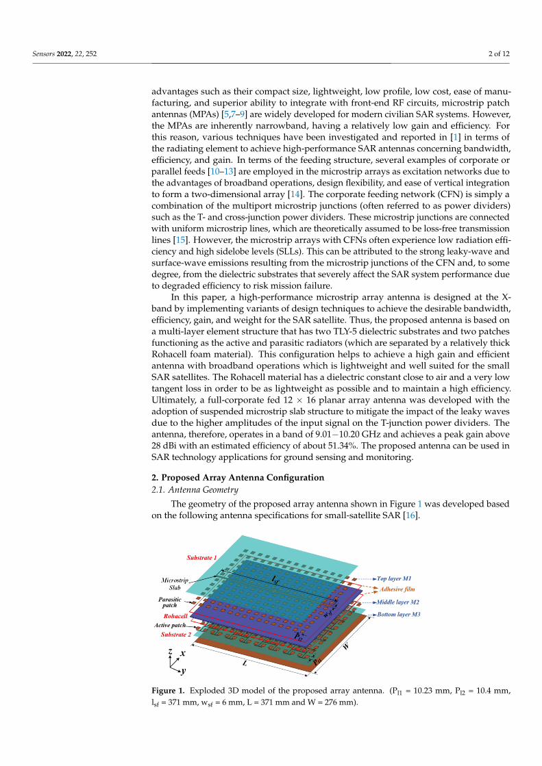
Figure 1. Exploded 3D model of the proposed array antenna. (Pl1 = 10.23 mm, Pl2 = 10.4 mm, lsf = 371 mm, wsf = 6 mm, L = 371 mm and W = 276 mm). Figure 1. Exploded 3D model of the proposed array antenna. (Pl1 = 10.23 mm, Pl2 = 10.4 mm,lsf = 371 mm, wsf = 6 mm, L = 371 mm and W = 276 mm).
Sensors 2022, 22, 252 3 of 12
• Antenna Size: (Az × El) 371 mm × 276 mm• Gain ≥ 28.5 dBi• Frequency: 9.65 GHz [BW: 300 MHz]• Efficiency > 50%• Reflection Coefficient ≤ −15 dB• Beamwidth: Az > 4.0, El > 5.8
• Sidelobe Level: Az < −13 dB, El < −13 dB• Polarization: linear (Vertical)• Port: SMA (F)• Antenna Panel Launch Mass: 0.53 kg
The antenna is a multilayered 12 × 16 array structure built on two dielectric substratesmade of Taconic TLY-5 (i.e., substrate 1 and substrate 2, εr = 2.2, tan δ = 0.0009) with arelatively thick Rohacell material (εr = 1.07, tan δ = 0.0017) sandwiched between them.The thickness of the two substrates is given as hsub1 = hsub2 = 0.508 mm. The antennacontains three copper layers (i.e., a top layer M1, middle layer M2, and bottom layerM3). In the structural design, the middle layer M2 constitutes the corporate-fed square-shaped microstrip patches that are employed due to their simple structure and generallygood performance, and they reside on the top surface of the lower substrate (as shown inFigure 1). These are the active patches that couple power electromagnetically through theRohacell material to the top layer, M1, consisting of parasitic square-shaped patches and asuspended microstrip slab structure at the backside of the upper substrate (i.e., substrate 1).The copper cladding at the bottom layer, M3, serves as the ground plane.
From the configuration of the proposed array antenna, as shown in Figure 1, it canbe seen that adhesive films are used as a bonding agent to glue the two TLY-5 dielectricsubstrates to the Rohacell material. With this configuration, the array antenna achieveshigh gain, high efficiency, and broadband performances more than many existing planararray antennas for SAR applications with stack-up topology. Meanwhile, the weight of theantenna is kept to the minimum owing to the lightweight property of the Rohacell foamlayer. A suspended microstrip slab structure is employed in the design to suppress anyparasitic radiations attributable to leaky waves from the central most power divider wheremost of the high-amplitude signals are concentrated.
2.2. Antenna Element Design
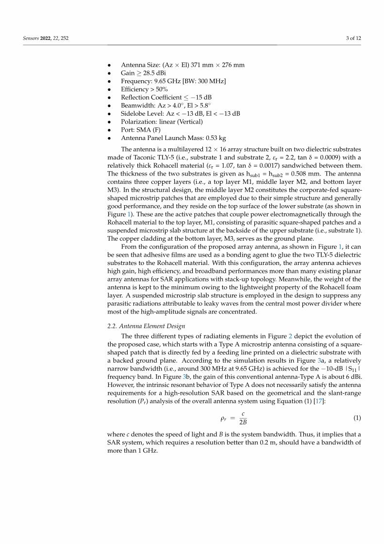
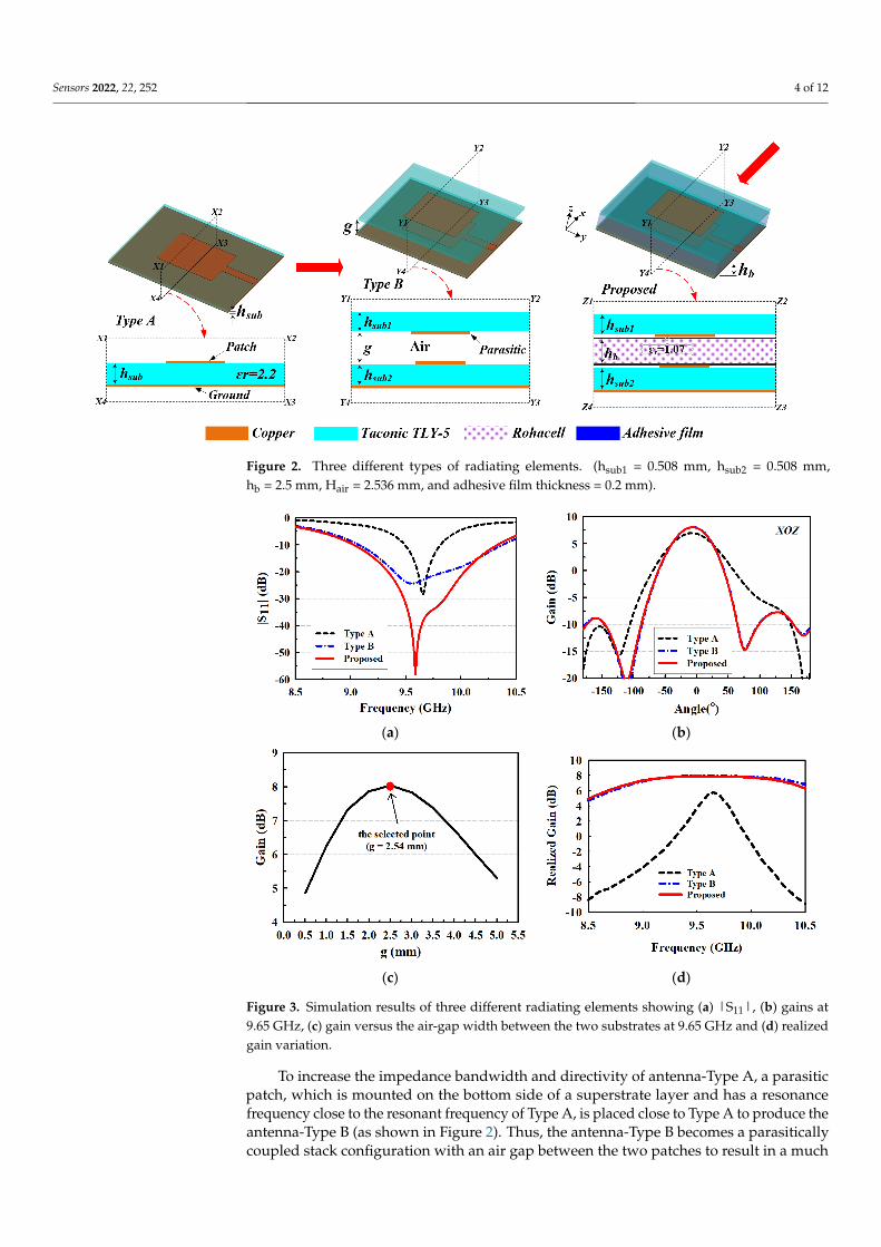
The three different types of radiating elements in Figure 2 depict the evolution ofthe proposed case, which starts with a Type A microstrip antenna consisting of a square-shaped patch that is directly fed by a feeding line printed on a dielectric substrate witha backed ground plane. According to the simulation results in Figure 3a, a relativelynarrow bandwidth (i.e., around 300 MHz at 9.65 GHz) is achieved for the −10-dB |S11|frequency band. In Figure 3b, the gain of this conventional antenna-Type A is about 6 dBi.However, the intrinsic resonant behavior of Type A does not necessarily satisfy the antennarequirements for a high-resolution SAR based on the geometrical and the slant-rangeresolution (Pr) analysis of the overall antenna system using Equation (1) [17]:
ρr =c
2B(1)
where c denotes the speed of light and B is the system bandwidth. Thus, it implies that aSAR system, which requires a resolution better than 0.2 m, should have a bandwidth ofmore than 1 GHz.
Sensors 2022, 22, 252 4 of 12Sensors 2022, 22, x FOR PEER REVIEW 4 of 12
Figure 2. Three different types of radiating elements. (hsub1 = 0.508 mm, hsub2 = 0.508 mm, hb = 2.5 mm, Hair = 2.536 mm, and adhesive film thickness = 0.2 mm).
(a) (b)
(c) (d)
Figure 3. Simulation results of three different radiating elements showing (a) |S11|, (b) gains at 9.65 GHz (c) gain versus the air-gap width between the two substrates at 9.65 GHz and (d) realized gain variation.
To increase the impedance bandwidth and directivity of antenna-Type A, a parasitic patch, which is mounted on the bottom side of a superstrate layer and has a resonance frequency close to the resonant frequency of Type A, is placed close to Type A to produce the antenna-Type B (as shown in Figure 2). Thus, the antenna-Type B becomes a parasiti-cally coupled stack configuration with an air gap between the two patches to result in a
Figure 2. Three different types of radiating elements. (hsub1 = 0.508 mm, hsub2 = 0.508 mm,hb = 2.5 mm, Hair = 2.536 mm, and adhesive film thickness = 0.2 mm).
Sensors 2022, 22, x FOR PEER REVIEW 4 of 12
Figure 2. Three different types of radiating elements. (hsub1 = 0.508 mm, hsub2 = 0.508 mm, hb = 2.5 mm, Hair = 2.536 mm, and adhesive film thickness = 0.2 mm).
(a) (b)
(c) (d)
Figure 3. Simulation results of three different radiating elements showing (a) |S11|, (b) gains at 9.65 GHz (c) gain versus the air-gap width between the two substrates at 9.65 GHz and (d) realized gain variation.
To increase the impedance bandwidth and directivity of antenna-Type A, a parasitic patch, which is mounted on the bottom side of a superstrate layer and has a resonance frequency close to the resonant frequency of Type A, is placed close to Type A to produce the antenna-Type B (as shown in Figure 2). Thus, the antenna-Type B becomes a parasiti-cally coupled stack configuration with an air gap between the two patches to result in a
Figure 3. Simulation results of three different radiating elements showing (a) |S11|, (b) gains at9.65 GHz, (c) gain versus the air-gap width between the two substrates at 9.65 GHz and (d) realizedgain variation.
To increase the impedance bandwidth and directivity of antenna-Type A, a parasiticpatch, which is mounted on the bottom side of a superstrate layer and has a resonancefrequency close to the resonant frequency of Type A, is placed close to Type A to produce theantenna-Type B (as shown in Figure 2). Thus, the antenna-Type B becomes a parasiticallycoupled stack configuration with an air gap between the two patches to result in a much
Sensors 2022, 22, 252 5 of 12
better bandwidth than Type A (as shown in Figure 3a). In addition, a higher gain can beobserved in the frequency band of 9.1–10.4 GHz (as shown in Figure 3b, Type B). Thus, bythe adjusting of the air-gap width, g, between the two patches, the parasitic patch appearsto direct the radiation from the active patch toward the boresight direction to maximize thedirectivity of the antenna (as reported in Figure 3c). The curve of the gain around 8 dBi isobtained when the value of g is around 2.54 mm. However, since it is impractical to suspendthe superstrate layer of Type B in air, the simplest approach to the design is to sandwich aRohacell structural foam between the two substrates with adhesive films bonding themtogether to achieve the proposed radiating element in Figure 2. The Rohacell material wasselected due to its low tangent loss of 0.0017 and lightweight property due to the fact thatits dielectric constant is similar to that of air. As a result, the proposed radiating elementexhibits a bandwidth performance similar to that of Type B, as shown in Figure 3a,b (i.e.,−10 dB |S11| bandwidth of 1.3 GHz). Again, from Figure 3d, it can be observed that bothType B and the proposed element antenna have a similar gain performance. Moreover, bothType B and the proposed antenna have a broader gain bandwidth compared to the Type A.
2.3. Array Design
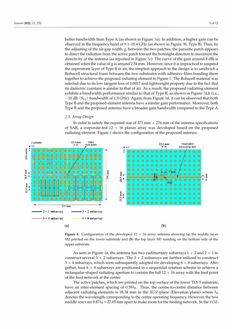
In order to satisfy the required size of 371 mm × 276 mm of the antenna specificationsof SAR, a corporate-fed 12 × 16 planar array was developed based on the proposedradiating element. Figure 4 shows the configuration of the proposed antenna.
Sensors 2022, 22, x FOR PEER REVIEW 5 of 12
much better bandwidth than Type A (as shown in Figure 3a). In addition, a higher gain can be observed in the frequency band of 9.1–10.4 GHz (as shown in Figure 3b, Type B). Thus, by the adjusting of the air-gap width, g, between the two patches, the parasitic patch appears to direct the radiation from the active patch toward the boresight direction to maximize the directivity of the antenna (as reported in Figure 3c). The curve of the gain around 8 dBi is obtained when the value of g is around 2.54 mm. However, since it is impractical to suspend the superstrate layer of Type B in air, the simplest approach to the design is to sandwich a Rohacell structural foam between the two substrates with adhe-sive films bonding them together to achieve the proposed radiating element in Figure 2. The Rohacell material was selected due to its low tangent loss of 0.0017 and lightweight property due to the fact that its dielectric constant is similar to that of air. As a result, the proposed radiating element exhibits a bandwidth performance similar to that of Type B, as shown in Figure 3a,b (i.e., −10 dB |S11| bandwidth of 1.3 GHz). Again, from Figure 3d, it can be observed that both Type B and the proposed element antenna have a similar gain performance. Moreover, both Type B and the proposed antenna have a broader gain band-width compared to the Type A.
2.3. Array Design In order to satisfy the required size of 371 mm × 276 mm of the antenna specifications
of SAR, a corporate-fed 12 × 16 planar array was developed based on the proposed radi-ating element. Figure 4 shows the configuration of the proposed antenna.
(a) (b)
Figure 4. Configuration of the developed 12 × 16 array antenna showing (a) the middle layer M2 printed on the lower substrate and (b) the top layer M1 residing on the bottom side of the upper substrate.
As seen in Figure 4a, the antenna has two rudimentary subarrays 1 × 2 and 2 × 1 to construct several 3 × 2 subarrays. The 3 × 2 subarrays are further utilized to construct 3 × 4 subarrays, which were subsequently adopted for developing 6 × 8 subarrays. Altogether, four 6 × 8 subarrays are positioned in a sequential rotation scheme to achieve a rectangu-lar-shaped radiating aperture to contain the full 12 × 16 array with the feed point of the feed network at the center.
The active patches, which are printed on the top surface of the lower TLY-5 substrate, have an inter-element spacing of 0.59λ0. Thus, the centre-to-centre distance between adja-cent radiating elements is 18.34 mm in the XOZ-plane (Elevation plane) where λ0 denotes the wavelength corresponding to the centre operating frequency,). However, the two mid-dle rows are 0.87λ0 = 27.05 mm apart to make room for the feeding network. In the YOZ-
Figure 4. Configuration of the developed 12 × 16 array antenna showing (a) the middle layerM2 printed on the lower substrate and (b) the top layer M1 residing on the bottom side of theupper substrate.
As seen in Figure 4a, the antenna has two rudimentary subarrays 1 × 2 and 2 × 1 toconstruct several 3 × 2 subarrays. The 3 × 2 subarrays are further utilized to construct3 × 4 subarrays, which were subsequently adopted for developing 6 × 8 subarrays. Alto-gether, four 6 × 8 subarrays are positioned in a sequential rotation scheme to achieve arectangular-shaped radiating aperture to contain the full 12 × 16 array with the feed pointof the feed network at the center.
The active patches, which are printed on the top surface of the lower TLY-5 substrate,have an inter-element spacing of 0.59λ0. Thus, the centre-to-centre distance betweenadjacent radiating elements is 18.34 mm in the XOZ-plane (Elevation plane) where λ0denotes the wavelength corresponding to the centre operating frequency. However, the twomiddle rows are 0.87λ0 = 27.05 mm apart to make room for the feeding network. In the YOZ-
Sensors 2022, 22, 252 6 of 12
plane (Azimuth plane), the patches assume a centre-to-centre spacing of 0.62λ0 = 19.27 mm,as shown in Figure 4a.
Similarly, the elemental spacing between the parasitic patches at the backside of theupper substrate is given as 18.34 mm in the XOZ-plane, as shown in Figure 4b. Meanwhile,they are separated by a distance of 19.27 mm in the YOZ-plane. The spacing between thetwo middle rows of parasitic patches in the XOZ-plane is given as 27.05 mm to align themwith their corresponding active patches.
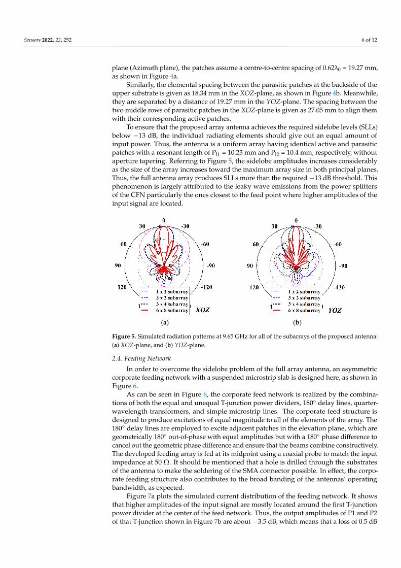
To ensure that the proposed array antenna achieves the required sidelobe levels (SLLs)below −13 dB, the individual radiating elements should give out an equal amount ofinput power. Thus, the antenna is a uniform array having identical active and parasiticpatches with a resonant length of Pl1 = 10.23 mm and Pl2 = 10.4 mm, respectively, withoutaperture tapering. Referring to Figure 5, the sidelobe amplitudes increases considerablyas the size of the array increases toward the maximum array size in both principal planes.Thus, the full antenna array produces SLLs more than the required −13 dB threshold. Thisphenomenon is largely attributed to the leaky wave emissions from the power splittersof the CFN particularly the ones closest to the feed point where higher amplitudes of theinput signal are located.
Sensors 2022, 22, x FOR PEER REVIEW 6 of 12
plane (Azimuth plane), the patches assume a centre-to-centre spacing of 0.62λ0 = 19.27 mm, as shown in Figure 4a.
Similarly, the elemental spacing between the parasitic patches at the backside of the upper substrate is given as 18.34 mm in the XOZ-plane, as shown in Figure 4b. Mean-while, they are separated by a distance of 19.27 mm in the YOZ-plane. The spacing be-tween the two middle rows of parasitic patches in the XOZ-plane is given as 27.05 mm to align them with their corresponding active patches.
To ensure that the proposed array antenna achieves the required sidelobe levels (SLLs) below −13 dB, the individual radiating elements should give out an equal amount of input power. Thus, the antenna is a uniform array having identical active and parasitic patches with a resonant length of Pl1 = 10.23 mm and Pl2 = 10.4 mm, respectively, without aperture tapering. Referring to Figure 5, the sidelobe amplitudes increases considerably as the size of the array increases toward the maximum array size in both principal planes. Thus, the full antenna array produces SLLs more than the required −13 dB threshold. This phenomenon is largely attributed to the leaky wave emissions from the power splitters of the CFN particularly the ones closest to the feed point where higher amplitudes of the input signal are located.
(a) (b)
Figure 5. Simulated radiation patterns at 9.65 GHz for all of the subarrays of the proposed antenna: (a) XOZ-plane, and (b) YOZ-plane.
2.4. Feeding Network In order to overcome the sidelobe problem of the full array antenna, an asymmetric
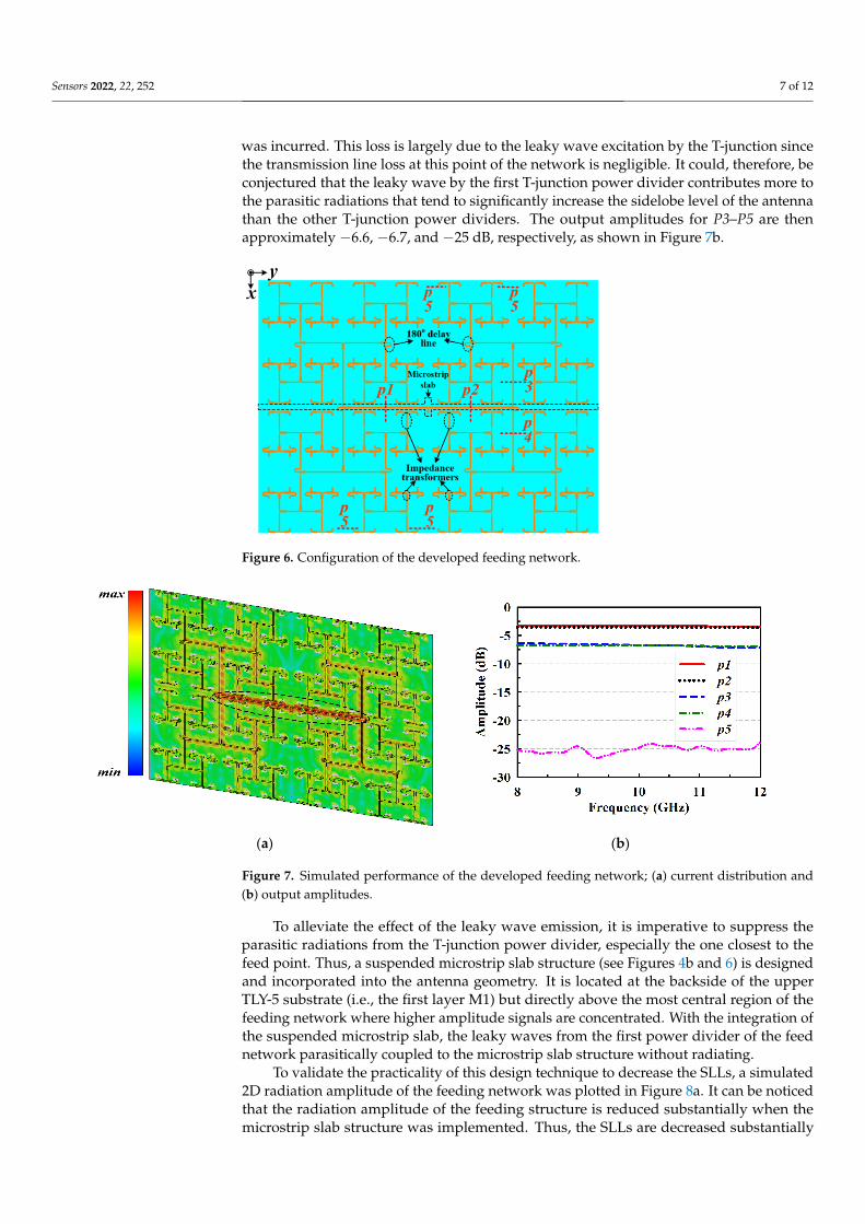
corporate feeding network with a suspended microstrip slab is designed here, as shown in Figure 6.
Figure 6. Configuration of the developed feeding network.
Figure 5. Simulated radiation patterns at 9.65 GHz for all of the subarrays of the proposed antenna:(a) XOZ-plane, and (b) YOZ-plane.
2.4. Feeding Network
In order to overcome the sidelobe problem of the full array antenna, an asymmetriccorporate feeding network with a suspended microstrip slab is designed here, as shown inFigure 6.
As can be seen in Figure 6, the corporate feed network is realized by the combina-tions of both the equal and unequal T-junction power dividers, 180 delay lines, quarter-wavelength transformers, and simple microstrip lines. The corporate feed structure isdesigned to produce excitations of equal magnitude to all of the elements of the array. The180 delay lines are employed to excite adjacent patches in the elevation plane, which aregeometrically 180 out-of-phase with equal amplitudes but with a 180 phase difference tocancel out the geometric phase difference and ensure that the beams combine constructively.The developed feeding array is fed at its midpoint using a coaxial probe to match the inputimpedance at 50 Ω. It should be mentioned that a hole is drilled through the substratesof the antenna to make the soldering of the SMA connector possible. In effect, the corpo-rate feeding structure also contributes to the broad banding of the antennas’ operatingbandwidth, as expected.
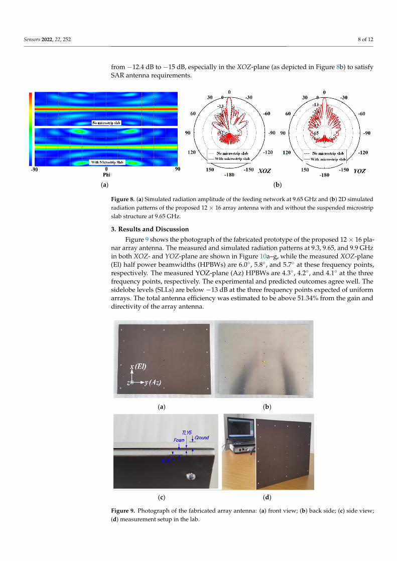
Figure 7a plots the simulated current distribution of the feeding network. It showsthat higher amplitudes of the input signal are mostly located around the first T-junctionpower divider at the center of the feed network. Thus, the output amplitudes of P1 and P2of that T-junction shown in Figure 7b are about −3.5 dB, which means that a loss of 0.5 dB
Sensors 2022, 22, 252 7 of 12
was incurred. This loss is largely due to the leaky wave excitation by the T-junction sincethe transmission line loss at this point of the network is negligible. It could, therefore, beconjectured that the leaky wave by the first T-junction power divider contributes more tothe parasitic radiations that tend to significantly increase the sidelobe level of the antennathan the other T-junction power dividers. The output amplitudes for P3–P5 are thenapproximately −6.6, −6.7, and −25 dB, respectively, as shown in Figure 7b.
Sensors 2022, 22, x FOR PEER REVIEW 6 of 12
plane (Azimuth plane), the patches assume a centre-to-centre spacing of 0.62λ0 = 19.27 mm, as shown in Figure 4a.
Similarly, the elemental spacing between the parasitic patches at the backside of the upper substrate is given as 18.34 mm in the XOZ-plane, as shown in Figure 4b. Mean-while, they are separated by a distance of 19.27 mm in the YOZ-plane. The spacing be-tween the two middle rows of parasitic patches in the XOZ-plane is given as 27.05 mm to align them with their corresponding active patches.
To ensure that the proposed array antenna achieves the required sidelobe levels (SLLs) below −13 dB, the individual radiating elements should give out an equal amount of input power. Thus, the antenna is a uniform array having identical active and parasitic patches with a resonant length of Pl1 = 10.23 mm and Pl2 = 10.4 mm, respectively, without aperture tapering. Referring to Figure 5, the sidelobe amplitudes increases considerably as the size of the array increases toward the maximum array size in both principal planes. Thus, the full antenna array produces SLLs more than the required −13 dB threshold. This phenomenon is largely attributed to the leaky wave emissions from the power splitters of the CFN particularly the ones closest to the feed point where higher amplitudes of the input signal are located.
(a) (b)
Figure 5. Simulated radiation patterns at 9.65 GHz for all of the subarrays of the proposed antenna: (a) XOZ-plane, and (b) YOZ-plane.
2.4. Feeding Network In order to overcome the sidelobe problem of the full array antenna, an asymmetric
corporate feeding network with a suspended microstrip slab is designed here, as shown in Figure 6.
Figure 6. Configuration of the developed feeding network. Figure 6. Configuration of the developed feeding network.
Sensors 2022, 22, x FOR PEER REVIEW 7 of 12
As can be seen in Figure 6, the corporate feed network is realized by the combinations of both the equal and unequal T-junction power dividers, 180° delay lines, quarter-wave-length transformers, and simple microstrip lines. The corporate feed structure is designed to produce excitations of equal magnitude to all of the elements of the array. The 180° delay lines are employed to excite adjacent patches in the elevation plane, which are geo-metrically 180° out-of-phase with equal amplitudes but with a 180° phase difference to cancel out the geometric phase difference and ensure that the beams combine construc-tively. The developed feeding array is fed at its midpoint using a coaxial probe to match the input impedance at 50 Ω. It should be mentioned that a hole is drilled through the substrates of the antenna to make the soldering of the SMA connector possible. In effect, the corporate feeding structure also contributes to the broad banding of the antennas’ op-erating bandwidth, as expected.
Figure 7a plots the simulated current distribution of the feeding network. It shows that higher amplitudes of the input signal are mostly located around the first T-junction power divider at the center of the feed network. Thus, the output amplitudes of P1 and P2 of that T-junction shown in Figure 7b are about −3.5 dB, which means that a loss of 0.5 dB was incurred. This loss is largely due to the leaky wave excitation by the T-junction since the transmission line loss at this point of the network is negligible. It could, therefore, be conjectured that the leaky wave by the first T-junction power divider contributes more to the parasitic radiations that tend to significantly increase the sidelobe level of the an-tenna than the other T-junction power dividers. The output amplitudes for P3–P5 are then approximately −6.6, −6.7, and −25 dB, respectively, as shown in Figure 7b.
(a) (b)
Figure 7. Simulated performance of the developed feeding network; (a) current distribution and (b) output amplitudes.
To alleviate the effect of the leaky wave emission, it is imperative to suppress the parasitic radiations from the T-junction power divider, especially the one closest to the feed point. Thus, a suspended microstrip slab structure (see Figures 4b and 6) is designed and incorporated into the antenna geometry. It is located at the backside of the upper TLY-5 substrate (i.e., the first layer M1) but directly above the most central region of the feeding network where higher amplitude signals are concentrated. With the integration of the sus-pended microstrip slab, the leaky waves from the first power divider of the feed network parasitically coupled to the microstrip slab structure without radiating.
To validate the practicality of this design technique to decrease the SLLs, a simulated 2D radiation amplitude of the feeding network was plotted in Figure 8a. It can be noticed that the radiation amplitude of the feeding structure is reduced substantially when the microstrip slab structure was implemented. Thus, the SLLs are decreased substantially
Figure 7. Simulated performance of the developed feeding network; (a) current distribution and(b) output amplitudes.
To alleviate the effect of the leaky wave emission, it is imperative to suppress theparasitic radiations from the T-junction power divider, especially the one closest to thefeed point. Thus, a suspended microstrip slab structure (see Figures 4b and 6) is designedand incorporated into the antenna geometry. It is located at the backside of the upperTLY-5 substrate (i.e., the first layer M1) but directly above the most central region of thefeeding network where higher amplitude signals are concentrated. With the integration ofthe suspended microstrip slab, the leaky waves from the first power divider of the feednetwork parasitically coupled to the microstrip slab structure without radiating.
To validate the practicality of this design technique to decrease the SLLs, a simulated2D radiation amplitude of the feeding network was plotted in Figure 8a. It can be noticedthat the radiation amplitude of the feeding structure is reduced substantially when themicrostrip slab structure was implemented. Thus, the SLLs are decreased substantially
Sensors 2022, 22, 252 8 of 12
from −12.4 dB to −15 dB, especially in the XOZ-plane (as depicted in Figure 8b) to satisfySAR antenna requirements.
Sensors 2022, 22, x FOR PEER REVIEW 8 of 12
from −12.4 dB to −15 dB, especially in the XOZ-plane (as depicted in Figure 8b) to satisfy SAR antenna requirements.
(a) (b)
Figure 8. (a) Simulated radiation amplitude of the feeding network at 9.65 GHz and (b) 2D simu-lated radiation patterns of the proposed 12 × 16 array antenna with and without the suspended microstrip slab structure at 9.65 GHz.
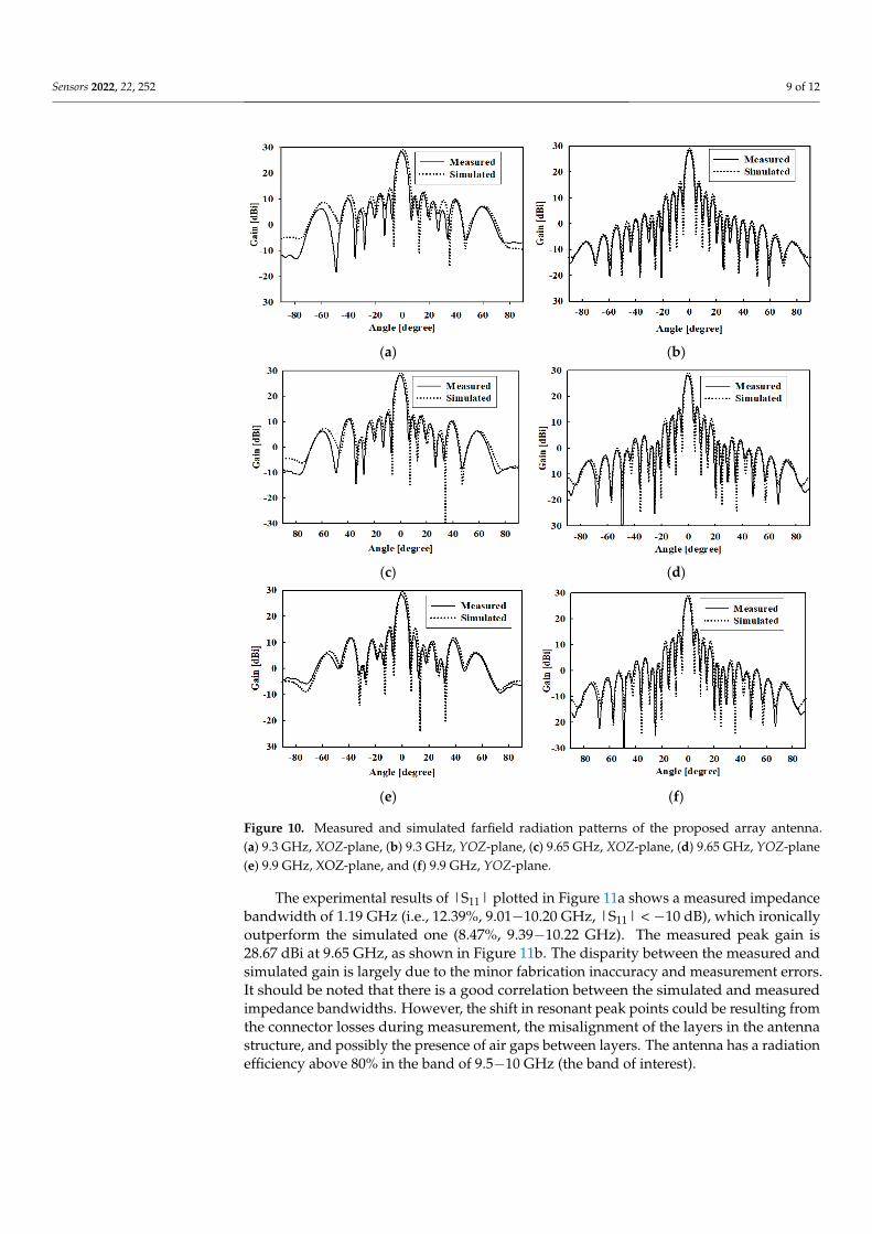
3. Results and Discussion Figure 9 shows the photograph of the fabricated prototype of the proposed 12 × 16
planar array antenna. The measured and simulated radiation patterns at 9.3, 9.65, and 9.9 GHz in both XOZ- and YOZ-plane are shown in Figure 10a–g, while the measured XOZ-plane (El) half power beamwidths (HPBWs) are 6.0°, 5.8°, and 5.7° at these frequency points, respectively. The measured YOZ-plane (Az) HPBWs are 4.3°, 4.2°, and 4.1° at the three frequency points, respectively. The experimental and predicted outcomes agree well. The sidelobe levels (SLLs) are below −13 dB at the three frequency points expected of uniform arrays. The total antenna efficiency was estimated to be above 51.34% from the gain and directivity of the array antenna.
(a) (b)
(c) (d)
Figure 9. Photograph of the fabricated array antenna: (a) front view; (b) back side; (c) side view; (d) measurement setup in the lab.
Figure 8. (a) Simulated radiation amplitude of the feeding network at 9.65 GHz and (b) 2D simulatedradiation patterns of the proposed 12 × 16 array antenna with and without the suspended microstripslab structure at 9.65 GHz.
3. Results and Discussion
Figure 9 shows the photograph of the fabricated prototype of the proposed 12 × 16 pla-nar array antenna. The measured and simulated radiation patterns at 9.3, 9.65, and 9.9 GHzin both XOZ- and YOZ-plane are shown in Figure 10a–g, while the measured XOZ-plane(El) half power beamwidths (HPBWs) are 6.0, 5.8, and 5.7 at these frequency points,respectively. The measured YOZ-plane (Az) HPBWs are 4.3, 4.2, and 4.1 at the threefrequency points, respectively. The experimental and predicted outcomes agree well. Thesidelobe levels (SLLs) are below −13 dB at the three frequency points expected of uniformarrays. The total antenna efficiency was estimated to be above 51.34% from the gain anddirectivity of the array antenna.
Sensors 2022, 22, x FOR PEER REVIEW 8 of 12
from −12.4 dB to −15 dB, especially in the XOZ-plane (as depicted in Figure 8b) to satisfy SAR antenna requirements.
(a) (b)
Figure 8. (a) Simulated radiation amplitude of the feeding network at 9.65 GHz and (b) 2D simu-lated radiation patterns of the proposed 12 × 16 array antenna with and without the suspended microstrip slab structure at 9.65 GHz.
3. Results and Discussion Figure 9 shows the photograph of the fabricated prototype of the proposed 12 × 16
planar array antenna. The measured and simulated radiation patterns at 9.3, 9.65, and 9.9 GHz in both XOZ- and YOZ-plane are shown in Figure 10a–g, while the measured XOZ-plane (El) half power beamwidths (HPBWs) are 6.0°, 5.8°, and 5.7° at these frequency points, respectively. The measured YOZ-plane (Az) HPBWs are 4.3°, 4.2°, and 4.1° at the three frequency points, respectively. The experimental and predicted outcomes agree well. The sidelobe levels (SLLs) are below −13 dB at the three frequency points expected of uniform arrays. The total antenna efficiency was estimated to be above 51.34% from the gain and directivity of the array antenna.
(a) (b)
(c) (d)
Figure 9. Photograph of the fabricated array antenna: (a) front view; (b) back side; (c) side view; (d) measurement setup in the lab. Figure 9. Photograph of the fabricated array antenna: (a) front view; (b) back side; (c) side view;(d) measurement setup in the lab.
Sensors 2022, 22, 252 9 of 12Sensors 2022, 22, x FOR PEER REVIEW 9 of 12
(a) (b)
(c) (d)
(e) (f)
Figure 10. Measured and simulated farfield radiation patterns of the proposed array antenna. (a) 9.3 GHz, XOZ-plane, (b) 9.3 GHz, YOZ-plane, (c) 9.65 GHz, XOZ-plane, (d) 9.65 GHz, YOZ-plane (e) 9.9 GHz, XOZ-plane, and (f) 9.9 GHz, YOZ-plane.
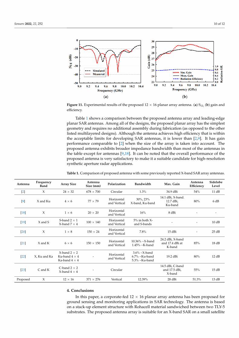
The experimental results of |S11| plotted in Figure 11a shows a measured impedance bandwidth of 1.19 GHz (i.e., 12.39%, 9.01−10.20 GHz, |S11| < −10 dB), which ironically outperform the simulated one (8.47%, 9.39−10.22 GHz). The measured peak gain is 28.67 dBi at 9.65 GHz, as shown in Figure 11b. The disparity between the measured and simu-lated gain is largely due to the minor fabrication inaccuracy and measurement errors. It should be noted that there is a good correlation between the simulated and measured impedance bandwidths. However, the shift in resonant peak points could be resulting from the connector losses during measurement, the misalignment of the layers in the an-tenna structure, and possibly the presence of air gaps between layers. The antenna has a radiation efficiency above 80% in the band of 9.5−10 GHz (the band of interest).
Figure 10. Measured and simulated farfield radiation patterns of the proposed array antenna.(a) 9.3 GHz, XOZ-plane, (b) 9.3 GHz, YOZ-plane, (c) 9.65 GHz, XOZ-plane, (d) 9.65 GHz, YOZ-plane(e) 9.9 GHz, XOZ-plane, and (f) 9.9 GHz, YOZ-plane.
The experimental results of |S11| plotted in Figure 11a shows a measured impedancebandwidth of 1.19 GHz (i.e., 12.39%, 9.01−10.20 GHz, |S11| < −10 dB), which ironicallyoutperform the simulated one (8.47%, 9.39−10.22 GHz). The measured peak gain is28.67 dBi at 9.65 GHz, as shown in Figure 11b. The disparity between the measured andsimulated gain is largely due to the minor fabrication inaccuracy and measurement errors.It should be noted that there is a good correlation between the simulated and measuredimpedance bandwidths. However, the shift in resonant peak points could be resulting fromthe connector losses during measurement, the misalignment of the layers in the antennastructure, and possibly the presence of air gaps between layers. The antenna has a radiationefficiency above 80% in the band of 9.5−10 GHz (the band of interest).
Sensors 2022, 22, 252 10 of 12Sensors 2022, 22, x FOR PEER REVIEW 10 of 12
(a) (b)
Figure 11. Experimental results of the proposed 12 × 16 planar array antenna. (a) S11; (b) gain and efficiency.
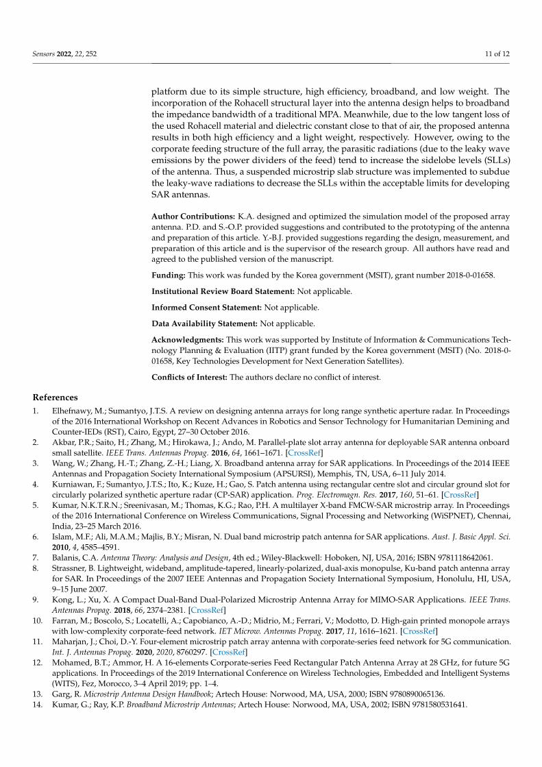
Table 1 shows a comparison between the proposed antenna array and leading-edge planar SAR antennas. Among all of the designs, the proposed planar array has the sim-plest geometry and requires no additional assembly during fabrication (as opposed to the other listed multilayered designs). Although the antenna achieves high efficiency that is within the acceptable limits for developing SAR antennas, it is lower than [2] and [9]. It has gain performance comparable to [2] when the size of the array is taken into account. The proposed antenna exhibits broader impedance bandwidth than most of the antennas in the table except for antennas [9] and [18]. It can be noted that the overall performance of the proposed antenna is very satisfactory to make it a suitable candidate for high-reso-lution synthetic aperture radar applications.
Table 1. Comparison of proposed antenna with some previously reported X-band SAR array anten-nas.
Antenna Frequency
Band Array Size Antenna
Size (mm) Polarization Bandwidth Max. Gain Antenna
Efficiency Sidelobe
Level [2] X 24 × 32 678 × 700 Circular 1.3% 34.9 dBi 54% 11 dB
[9] X and Ku 4×6 77 × 79 Horizontal
and Vertical 30%, 23% X-
band, Ku-band
14.1 dBi, X-band.
12.7 dBi, Ku-band
80% 6 dB
[18] X 1 × 6 20 × 20 Horizontal and Vertical
16% 8 dBi - -
[19] X and S S-band 2 × 1 X-band 7 × 4 100 × 140
Horizontal and Vertical
5% in both X- and S-bands - - 10 dB
[20] X 1 × 8 150 × 24 Horizontal
and Vertical 7.8% 15 dBi - 25 dB
[21] X and K 6 × 6 150 × 150 Horizontal
and Vertical 10.36% ~X-band 1.45% ~K-band
24.2 dBi, X-band and 17.4 dBi at K-band
85% 18 dB
[22] X, Ku and Ka
X-band 2 × 2 Ku-band 4 × 4 Ka-band 4 × 4
- Horizontal and Vertical
3.6% ~X-band 6.7% ~Ku-band 5.3% ~Ku-band
19.2 dBi 80% 12 dB
[23] C and K C-band 2 × 2 X-band 4 × 4 - Circular
14.5 dBi, C-band and 17.5 dBi, X-band
55% 15 dB
Proposed X 12 × 16 371 × 276 Vertical 12.39% 28 dBi 51.3% 13 dB
Figure 11. Experimental results of the proposed 12 × 16 planar array antenna. (a) S11; (b) gain andefficiency.
Table 1 shows a comparison between the proposed antenna array and leading-edgeplanar SAR antennas. Among all of the designs, the proposed planar array has the simplestgeometry and requires no additional assembly during fabrication (as opposed to the otherlisted multilayered designs). Although the antenna achieves high efficiency that is withinthe acceptable limits for developing SAR antennas, it is lower than [2,9]. It has gainperformance comparable to [2] when the size of the array is taken into account. Theproposed antenna exhibits broader impedance bandwidth than most of the antennas inthe table except for antennas [9,18]. It can be noted that the overall performance of theproposed antenna is very satisfactory to make it a suitable candidate for high-resolutionsynthetic aperture radar applications.
Table 1. Comparison of proposed antenna with some previously reported X-band SAR array antennas.
Antenna FrequencyBand Array Size Antenna
Size (mm) Polarization Bandwidth Max. Gain AntennaEfficiency
SidelobeLevel
[2] X 24 × 32 678 × 700 Circular 1.3% 34.9 dBi 54% 11 dB
[9] X and Ku 4 × 6 77 × 79 Horizontaland Vertical
30%, 23%X-band, Ku-band
14.1 dBi, X-band.12.7 dBi,Ku-band
80% 6 dB
[18] X 1 × 6 20 × 20 Horizontaland Vertical 16% 8 dBi - -
[19] X and S S-band 2 × 1X-band 7 × 4 100 × 140 Horizontal
and Vertical5% in both X-and S-bands - - 10 dB
[20] X 1 × 8 150 × 24 Horizontaland Vertical 7.8% 15 dBi - 25 dB
[21] X and K 6 × 6 150 × 150 Horizontaland Vertical
10.36% ~X-band1.45% ~K-band
24.2 dBi, X-bandand 17.4 dBi at
K-band85% 18 dB
[22] X, Ku and KaX-band 2 × 2
Ku-band 4 × 4Ka-band 4 × 4
- Horizontaland Vertical
3.6% ~X-band6.7% ~Ku-band5.3% ~Ku-band
19.2 dBi 80% 12 dB
[23] C and K C-band 2 × 2X-band 4 × 4 - Circular
14.5 dBi, C-bandand 17.5 dBi,
X-band55% 15 dB
Proposed X 12 × 16 371 × 276 Vertical 12.39% 28 dBi 51.3% 13 dB
4. Conclusions
In this paper, a corporate-fed 12 × 16 planar array antenna has been proposed forground sensing and monitoring applications in SAR technology. The antenna is basedon a stack-up element structure with Rohacell material sandwiched between two TLY-5substrates. The proposed antenna array is suitable for an X-band SAR on a small satellite
Sensors 2022, 22, 252 11 of 12
platform due to its simple structure, high efficiency, broadband, and low weight. Theincorporation of the Rohacell structural layer into the antenna design helps to broadbandthe impedance bandwidth of a traditional MPA. Meanwhile, due to the low tangent loss ofthe used Rohacell material and dielectric constant close to that of air, the proposed antennaresults in both high efficiency and a light weight, respectively. However, owing to thecorporate feeding structure of the full array, the parasitic radiations (due to the leaky waveemissions by the power dividers of the feed) tend to increase the sidelobe levels (SLLs)of the antenna. Thus, a suspended microstrip slab structure was implemented to subduethe leaky-wave radiations to decrease the SLLs within the acceptable limits for developingSAR antennas.
Author Contributions: K.A. designed and optimized the simulation model of the proposed arrayantenna. P.D. and S.-O.P. provided suggestions and contributed to the prototyping of the antennaand preparation of this article. Y.-B.J. provided suggestions regarding the design, measurement, andpreparation of this article and is the supervisor of the research group. All authors have read andagreed to the published version of the manuscript.
Funding: This work was funded by the Korea government (MSIT), grant number 2018-0-01658.
Institutional Review Board Statement: Not applicable.
Informed Consent Statement: Not applicable.
Data Availability Statement: Not applicable.
Acknowledgments: This work was supported by Institute of Information & Communications Tech-nology Planning & Evaluation (IITP) grant funded by the Korea government (MSIT) (No. 2018-0-01658, Key Technologies Development for Next Generation Satellites).
Conflicts of Interest: The authors declare no conflict of interest.
References1. Elhefnawy, M.; Sumantyo, J.T.S. A review on designing antenna arrays for long range synthetic aperture radar. In Proceedings
of the 2016 International Workshop on Recent Advances in Robotics and Sensor Technology for Humanitarian Demining andCounter-IEDs (RST), Cairo, Egypt, 27–30 October 2016.
2. Akbar, P.R.; Saito, H.; Zhang, M.; Hirokawa, J.; Ando, M. Parallel-plate slot array antenna for deployable SAR antenna onboardsmall satellite. IEEE Trans. Antennas Propag. 2016, 64, 1661–1671. [CrossRef]
3. Wang, W.; Zhang, H.-T.; Zhang, Z.-H.; Liang, X. Broadband antenna array for SAR applications. In Proceedings of the 2014 IEEEAntennas and Propagation Society International Symposium (APSURSI), Memphis, TN, USA, 6–11 July 2014.
4. Kurniawan, F.; Sumantyo, J.T.S.; Ito, K.; Kuze, H.; Gao, S. Patch antenna using rectangular centre slot and circular ground slot forcircularly polarized synthetic aperture radar (CP-SAR) application. Prog. Electromagn. Res. 2017, 160, 51–61. [CrossRef]
5. Kumar, N.K.T.R.N.; Sreenivasan, M.; Thomas, K.G.; Rao, P.H. A multilayer X-band FMCW-SAR microstrip array. In Proceedingsof the 2016 International Conference on Wireless Communications, Signal Processing and Networking (WiSPNET), Chennai,India, 23–25 March 2016.
6. Islam, M.F.; Ali, M.A.M.; Majlis, B.Y.; Misran, N. Dual band microstrip patch antenna for SAR applications. Aust. J. Basic Appl. Sci.2010, 4, 4585–4591.
7. Balanis, C.A. Antenna Theory: Analysis and Design, 4th ed.; Wiley-Blackwell: Hoboken, NJ, USA, 2016; ISBN 9781118642061.8. Strassner, B. Lightweight, wideband, amplitude-tapered, linearly-polarized, dual-axis monopulse, Ku-band patch antenna array
for SAR. In Proceedings of the 2007 IEEE Antennas and Propagation Society International Symposium, Honolulu, HI, USA,9–15 June 2007.
9. Kong, L.; Xu, X. A Compact Dual-Band Dual-Polarized Microstrip Antenna Array for MIMO-SAR Applications. IEEE Trans.Antennas Propag. 2018, 66, 2374–2381. [CrossRef]
10. Farran, M.; Boscolo, S.; Locatelli, A.; Capobianco, A.-D.; Midrio, M.; Ferrari, V.; Modotto, D. High-gain printed monopole arrayswith low-complexity corporate-feed network. IET Microw. Antennas Propag. 2017, 11, 1616–1621. [CrossRef]
11. Maharjan, J.; Choi, D.-Y. Four-element microstrip patch array antenna with corporate-series feed network for 5G communication.Int. J. Antennas Propag. 2020, 2020, 8760297. [CrossRef]
12. Mohamed, B.T.; Ammor, H. A 16-elements Corporate-series Feed Rectangular Patch Antenna Array at 28 GHz, for future 5Gapplications. In Proceedings of the 2019 International Conference on Wireless Technologies, Embedded and Intelligent Systems(WITS), Fez, Morocco, 3–4 April 2019; pp. 1–4.
13. Garg, R. Microstrip Antenna Design Handbook; Artech House: Norwood, MA, USA, 2000; ISBN 9780890065136.14. Kumar, G.; Ray, K.P. Broadband Microstrip Antennas; Artech House: Norwood, MA, USA, 2002; ISBN 9781580531641.

Sensors 2022, 22, 252 12 of 12
15. Jam, S.; Malekpoor, H. Analysis on wideband patch arrays using unequal arms with equivalent circuit model in X-band. IEEEAntennas Wirel. Propag. Lett. 2016, 15, 1861–1864. [CrossRef]
16. Pyne, B.; Saito, H.; Akbar, P.R.; Hirokawa, J.; Tomura, T.; Tanaka, K. Development and performance evaluation of small SARsystem for 100-kg class satellite. IEEE J. Sel. Top. Appl. Earth Obs. Remote Sens. 2020, 13, 3879–3891. [CrossRef]
17. Alibakhshikenari, M.; Virdee, B.S.; See, C.H.; Abd-Alhameed, R.; Falcone, F.; Limiti, E. Array Antenna for Synthetic ApertureRadar Operating in X and KuBands: A Study to Enhance Isolation Between Radiation Elements. In Proceedings of the 12thEuropean Conference on Synthetic Aperture Radar, Aachen, Germany, 4–7 June 2018.
18. Qu, X.; Zhong, S.; Zhang, Y.; Wang, W. Design of an S/X dual-band dual-polarised microstrip antenna array for SAR applications.IET Microw. Antennas Propag. 2007, 1, 513–517. [CrossRef]
19. Capece, P.; Lucci, L.; Pelosi, G.; Porfilio, M.; Righini, M.; Steffè, W. A Multilayer PCB Dual-Polarized Radiating Element for FutureSAR Applications. IEEE Antennas Wirel. Propag. 2014, 13, 297–300. [CrossRef]
20. Zhao, X.; Tian, B.N.; Yeo, S.P.; Ong, L.C. Design of low-profile broadband dual-polarized integrated patch sub-array for X-bandSAR payload on small satellite. In Proceedings of the 2016 IEEE-APS Topical Conference on Antennas and Propagation inWireless Communications (APWC), Cairns, Australia, 19–23 September 2016; pp. 27–29.
21. Kothapudi, V.K.; Kumar, V. Hybrid-fed shared aperture antenna array for X/K-band airborne synthetic aperture radar applications.IET Microw. Antennas Propag. 2021, 15, 93–102. [CrossRef]
22. Mao, C.-X.; Gao, S.; Luo, Q.; Rommel, T.; Chu, Q.-X. Low-cost X/ku/Ka-band dual-polarized array with shared aperture. IEEETrans. Antennas Propag. 2017, 65, 3520–3527. [CrossRef]
23. Mao, C.-X.; Gao, S.; Wang, Y.; Chu, Q.-X.; Yang, X.-X. Dual-band circularly polarized shared-aperture array for C-/X-band satellitecommunications. IEEE Trans. Antennas Propag. 2017, 65, 5171–5178. [CrossRef]
Related Documents