el. Ss PAGES hea. ty VISE CR OR Te GR AD HUM GEA) a ie o be : 2 g « 3

Welcome message from author
This document is posted to help you gain knowledge. Please leave a comment to let me know what you think about it! Share it to your friends and learn new things together.
Transcript

el. Ss
PAGEShea. tyVISE CR OR Te GR AD HUMGEA)
aieobe
:2g«3
CL GObLTE
R-600
CONTROL, GUIDANCE, AND NAVIGATION FORADVANCED MANNED MISSIONS
(Final Report on Task II of Contract NAS-9-6823)
VOL. J} MULTIPROCESSOR COMPUTER SUBSYSTEM
JANUARY 1968
INSTRUMENTATION LABORATORYMASSACHUSETTSINSTITUTE OF TECHNOLOGY
CAMBRIDGE, MASSACHUSETTS
Approved!
_
Yen Kt “ote:iJon 6B
SHOyo FLANDERS, DIRECTOR, “ADVANGEDCGENCG&NOLYZO
APOL GUIDANCE AND NAVIGATION PROGRAM
_ Approved: Date:LZ (JanG§DAVID G. HOAG,APOLLO GUIDANCE AND NA ATION PROGRAM
3 ” ro 4 DB.
Approved:_(4,hick Ke Magen Date:SeeeRALPH R. RAGAN, DEPUTYDIRECTORINSTRUMENTATION LABORATORY
ACKNOWLEDGEMENT
This report was prepared under DSR Project 55-29440, sponsored by the Manned
Spacecraft Center of the National Aeronautics and Space Administration through
Contract NAS 9-4065 withthe Instrumentation Laboratory, Massachusetts Institute
of Technology, Cambridge, Mass.
This volume is the work of the following authors:
Chapter I Ramon Alonso, Albert Hopkins, and Herbert Thaler,
ChapterII Herbert Thaler, Albert Hopkins, Alan Green,; Robert Filene, James Miller, Darrow Lebovici,
and Robert Travis.
Chapter III Albert Hopkins, Kent Briggs, and Bruce Barrett.
Chapter IV John McKenna, Robert Scott, Donald Kadish,Robert Tove, Thomas Danegan, Jayne Partridge,David Hanley,. Thomas Zulon, and Jocob Martina.
The publication of this report does not constitute approval by the National
Aeronautics and Space Administration of the findings or the conclusions contained
therein. It is published only for the exchange and stimulation ofideas.
ii.
R-600
CONTROL, GUIDANCE AND NAVIGATION FOR
ADVANCEL MANNED MISSIONS
(Final Report on Task II of Contract NAS-9-6823)
ABSTRACT
This is a study of Navigation, Guidance, and Control for Advanced Manned
Space Missions, It is divided into the areas of systems, computer subsystems,
radiation subsystems, and inertial subsystems. From a system aspect a study is
made of guidance and navigation requirements imposed by the different phases of
interplanetary missions. A representative system is described as a design model.
Detailed descriptions are provided of analytical and development work on advanced
concepts in computer, radiation, and inertial subsystems.
It is shown that required system performance advances are well within rea-
son but that the requirements for reliability will demand new standards in design
concepts, quality assurance, maintainability, and quiescent failure rates.
Guidelines for further developments in this direction are set forth.
January 1968
ili
GE BLANK NOT FILMED.
PRECEDING PA
TABLE OF CONTENTS
INTRODUCTION
1, COMPUTER DESIGN CONCEPT
1,1
1,2
1,3
1,4
Apollo Experience
Requirements for an Advanced Computer
Fundamental Choices
Collaborative Multiprocessor Concept
COMPUTER SYSTEM/LOGICAL DESIGN
2.1
2,2
2,3
2.4
2.6
2.6
2.7
System and Subsystem Communications
Data Memory
Instruction Memory
Processor
Job Control and Executive Services
Input-Output Buffer
Programming Aids
COMPUTER LOGICAL/ELECTRICAL DESIGN
3.1
3.2
3.3
Processor Design
Memory Design
Bus Design
ELECTRICAL/MECHANICAL DESIGN.
4.1
4,2
4.3
4.4
Braid Memory
Plated Wire Memory
Integrated Circuits
Interconnections and Packaging
Pages
vii
1-1
1-4
1-9
1-10
2-1
2-17
2-28
2-31
2-54
2-79
2-83
3-1
3-17
3-20
4-1
4-35
4-82
4-86

TABLE OF CONTENTS(Cont'd)
Pages
5, CONCLUSIONS AND RECOMMENDATIONS ‘
5,1 The Role of Computer Research and Development 5-1
5,2 Simulations 5-1
5.3 Prototype Fabrication 5-2
5.4 Advanced Circuit Development 5-2
vi
VOLUME I
MULTIPROCESSOR COMPUTER SUBSYSTEMS
FOR ADVANCED MANNED SPACE MISSIONS
INTRODUCTION
VolumeII of R-600 is concerned with the development of computer subsystems
for advanced manned space mission. The work reported in this volume was performed
under Part II, Task IV, of contract NAS-9-6823 between the NASA Manned Spacecraft
Center and the Massachusetts Institute of Technology Instrumentation Laboratory.
General requirements for advanced manned missions upon Control, Guidance,
and Navigation Systems are set forth in Volume I of R-600. In that volume, a report
is made of a general study of the overall requirements for advanced manned missions
involving a range of exploratory missions in the solar system following the Apollo
and Apollo Applications Category of missions.
In this volume, there is set forth in greater detail the results of a ten-month's
effort to investigate various aspects of advanced technology applicable to computer
subsystems for advanced manned missions, etc.
vii
1, COMPUTER DESIGN CONCEPT
1,1 Apollo Experience
1.1.1 General Goals
The design of a computer for the Advanced Guidance System forces a
number of initial choices regarding goals, system capability, likely state of
relevant technologies at the time of implementation, and broad character of
the possible missions. Much of the initial design is choosing from among
imponderables and agreeing, among the designers and with the program spcn-
sors, upon general goals.
Several characteristics of an Advanced System can be identified for
possible exploration or special consideration, The first of these is the
fortunate independence of many of the tasks likely to be required simultaneously,
Unlike a massive matrix inversionproblem, in which every element affects
every element of the answer, an Advanced System will require simultaneous
maintenance of many control loops which are either independent or nested in
each other. An accompanying characteristic is likely to be that the control
loops to be served will not, on the whole, be of much greater speed than those
of Apollo. What is likely to be true is that the number of such loops will be
greater by an order of magnitude (or more) than is the case presently. The
general trend is toward more functions to be performed by the computer, rather
than very much faster functions.
A second characteristic of great importance is the lack of initial know-
ledge as to the true requirements of an Advanced System Computer. This can
be translated into a desire for a system which can be either expanded or
contracted at a late date in the project. Being able to change size is especially
important if it is possible to gain reliability by adding equipment,
A numberof other goals will be developed further on, as the various
areas of choice are identified and narrowed down, It is difficult to categorize
a computer both briefly and accurately. In this context it seems appropriate,
if not wholly adequate, to speak of an advanced computer in terms of perfarmance
of the present Apollo Guidance Computer, The advanced computer is to be
capable of improving upon AGC performance by a factor of ten (minimum),
and it is this measure that we choose as a general goal.
1.1.2 Specific Characteristics
A numberof lessons have been learned, some twice, which bear.dis-
cussing, These lessons have less to do with what we should have done in
Apollo than with identifying desirable characteristics.
1-1
1,1,2.1 Memory
One clear lesson is the impossiblity of a priori sizing of the computer
especially with regard to memory capacity, The original (1961) Apollo
memory capacity estimate was 4, 000 words, and it is felt by programmers
to be barely adequate. Memory was increased primarily because of
improvements in fixed memory technology, which allowed designs that
placed necessarily larger capacity memories in the same volume,
The need of a larger capacity memory did not become obvious until
long after Block IT was designed, at which time it was felt that 34, 000 words
was ample by perhaps as much as 50%. As of this writing the AGC
Block II logical structure makes it very difficult to add memory beyond
64, 000 words, even if such memories become physically compact enough.
The lessons are clear, Program memory has been grossly under-
estimated in the past, and designers are only partly wiser now as to required
sizes, This experience, together with uncertainties in missions for the
proposed system leads us to expect that memory size will be underestimated
again in the future. A second lesson is that it is essential to provide room
(in the form of adequate address fields) for memory size far beyondthose
physically practical today.
One of the reasons for underestimating memory sizes is the need for
varying degrees of automatic programming. It is not desirable, as was
done in Apollo, to minimize equipment by requiring programmers to be
clever and ingenious. As programs becomelarge the need for standariza-
tion, clarity and ease of checking increases, Furthermore, it becomes
impractical to generate hand coded pragrams; compilers as well as
assemblers become necessary, which in turn increase further the need
for memory because of compiler ineffciencies.,
1.1.2.2 SpeedThe AGC is, by now,’ some five to ten times slower than more
recent equivalent earth bound computers. Speed of future designs will
increase because of component improvement, without having to sacrifice
much else. Speed has not been as serious a problem in Apollo as mem-
ory capacity, but it should increase considerably in the future for a number
of reasons. Foremost is the partial equivalence of programs and special
purpose hardware, such as for floatingpoint arithmetic; having sufficient
speed permits a choice of implementationnot otherwise available.
Another obvious reason for higher speed is the ability to handle more
simultaneous tasks. Both of these reasons reflect Apollo experience,
A third reason for expecting higher speed is that it may be difficult not to
get it, given the improvement in performance of components and assembly
techniques. . oe
1-2.
There is one aspect of speed, however, which discourages its
choice as an unqualified goal, and that is power comsumption. Higher
speeds are obtained by overcoming reactance, (usually capacitive),
which usually requires larger power levels for signals. Fortunately the
expected increase in component speed comes about in great measure
because of miniaturization and decrease in physical dimensions, so that
we may expect the speed to power ratio to increase. Nevertheless,
allovrable power consumption will always be a consideration which
influences the eventual system performance,
1.1.2.3 Programming
Programming aids are possibly even more important for tomorrow's
ACGN system then improved memory technology. Scaling alone is said
to account for one third of the time, effort and people required to program
an Apollo sized mission, and it is clearly false economy to minimize
hardware at the expense of programming eage.
The desire for programming does not stop at flight programs, A ,
large body of auxiliary software for assembling, compiling, checking and
simulating must exist, and be planned concurrently with flight software
design; and here again designers are often faced with the choice of
minimizing one at the expense of complicating another. Previous emphasis
on minimization of flight hardware to the exclusion of other considerations
is no longer appropriate, and, with advancés in hardware technology, no
longer as necessary.
1.1.2.4 Interface Flexibility
Using (or trying to use) the Apollo input-output structure in circum-
stances other than the initially intended ones has been a recurring prob-
lem. Those interfaces were designed with a very specific environment
in mind(with the IMU, optics, DSKY) and when various parties explored
the possibility of adding non-G&N functions to the list performed by the
-AGC, the stumbling block would usually prove to be input-output limita-
tions. The inpit-output structure could have been generalized, by pro-~
viding high speed channelssimilar to those of commercial machines.
Once again, equipment minimization was-obtained at the cost of generality
of use. Because of the continuing dramatic decrease in equipment cost
(in dollars, space, weight) and increase in performance, a more general
solution to the input-output problem can be nowconsidered, —
One fact which stands out in relation to input-output is the high cost
of cabling and connectors, Cable harnesses now account for a substantial
portion of bulk and weight of equipment, and seriously detract from
reliable performance, Minimizing cabling, as well as improving it, is
desirable.
1.1.2.5 Reliability
Reliability in the Apollo Guidance Computer has been measured as a
mean-time-between-failures of the order of thousands ofhours, sufficient
for the Apollo lunar mission. Measuring the MTBF becomes moredifficult
as it increases owing to the need for longer measurement times and/or
larger sample sizes, Using the MTBF as a measure of reliability also
becomes less clearly valid because of differences of opinion as to the rele~
vance of certain failures, such as those caused by improper use and those
suffered «daring factory test.
The MTBF required for extended missions far exceeds that required
in Apollo. Beyond that, even if the Apollo MTBF were high enough, there
is an intuitive feeling that a device in which all parts must work is in-
sufficiently reliable in a mission where its function is critical to survival
and success. A certain measure of failures must be allowable without
causing the mission to end.
1.2 Requirements for an Advanced Computer
The major goal is to design a system capable of one hundred fold performance
in AGC terms. This may be viewed as a maximumif the system is held to be variable
in size, in which case the goal becomesone of a system which performs from ten fold
to a hundred fold AGC performance. The lower limit is a reflection of the speed im-
provement due solely to faster components.
It has become necessary to elaborate onsuch a general goal in termsof the
various relevant computer characteristics. A concrete goal, even if somewhat
arbitrary, is the proper way to relate and compare alternatives that arise in the
process of design.
1.2.1 Instruction RateThe AGC executes 15 bit instructions at an average rate of one every
24 usec, which is about 2/3 bit per usec. Ignoring for the moment such
questions as the relative efficiency of differing instruction sets, an Advanced
System computer should be capable of "consuming" instructions at an average
rate of 66 bits per sec. As will be seen later, it may not be desirable to -
preserve a classical computer structure, which may in turn make less obvious
what is meant by average consumption of program words, but it is nevertheless
very useful to consider computer performance in those terms.
One test against reality is to compare the desired bit rate of 66 megabits
per second with present memory technology. Commercial core memories are
capable of cycle times well below 1 uw sec, with word lengths of up to 72 bits;
MIT's own Rraid memory, which is read-only, is capable of 256 bits every two
or three y sec. In either case, existing memory technology is un to our demands
of it.
The effect of instructions more powerful than the relatively primitive
ones of the AGC cannot be easily assessed, in the sense that we cannot readily
estimate an equivalence between instruction bit rates and instruction power,
The difficulty arises because we do not know the relative usage of instructions;
we can estimate what a double precision, floating point vector cross product
instruction requires when implemented as an AGC subroutine, and hence, if
the advanced computer had such an instruction expressed as a 30 bit word, and
the AGC equivalent were a 100 word program (at 15 bits per word) then the
bit-flow ratio would be 30 to 1500, or 1 tp 50. This would hardly meanthatevery instruction bit of the advanced computer is 50 times more powerful than
an AGC instruction bit; to assesthat ratio we must make the same calculation
for every instruction of the new computer, and then obtain a weighted average
which depends on instruction usage. All we can say is that the bit rates out of
program memory are then minimized, To be safe in estimating advanced |
computer requirements we shall assume that all instruction bits have the same
relative power.
1.2.2 Memory Size: As (was discussed earlier, misestimation of required amounts of memory
are the rule rather than the exception, and always on the deficit side. Using the
one hundred-fold figure we may state that an advanced computer should have of
the.order of 60 X 10° bits of storage for programs and about 3.2 X 10° bits for
data (the AGC has 600, 000 and 32,000 respectively). It is certainly time that
we provide addressing capability for even larger memories than those.
The 60 million program bits do not imply, fortunately, the verylarge
volume that results were one to implement it with a random access store, Ifa
the braid were used (the densest form of random access memory we know of),
_and used exclusively, that much storage would require of the order of 6 cubic feet,
But combinations such as fixed memory (for safety), core memory (for flexibility
and speed) and tape (for bulkstorage at high densities) can provide us with what we
need,

It would not be sensible to require that an advanced computer have that
much storage in its first implementation. We can start out very much smaller,
But it is sensible to plan so as to be able to later implement and use such larger
memories, Our past record of underestimating should not be forgotten,
1.2.3 Input - Output Bandwidth
Another critical estimate is that of the total input - output activity to be
expected in a future system, measured as an overall bit rate. As an initial
estimate we will hold to the hundred-fold AGC concept.
As an average bit rate (even during periods of activity) the total input -
output activity of the AGC is surprisingly small, well below 5 Kpps. Under
worst case conditions the bit rate could be 100 Kpps, but these conditions are
not realizable because the overall system cannot respond to them, Worst case
conditions would require that every Coupling Data Unit be slewed at
maximum rate, and that maximum acceleration prevail in all axes. The Apollo
system is based on incremental encoders which send the computer one pulse
for every bit of change, a system whichrequires little bandwidth during normal
conditions and much during maximum activity conditions. A whole number
transfer system, in which devices are interrogated by the computer and answer
with whole numbersis better for high activity conditions, worse for normal ones,
At any rate, it is probably reasonable to argue for an output bandwidth of the
order of 5 to 10 Mpps, which is both technically reasonable and consonant with
the assumption of one hundred-fold the AGC observed rates.
' There is another way of looking at input-output requirements, a way
which is analogous to the telephone traffic grade of service concept. Briefly,
this requirement is expressed as a reaction time of the computer to an external
stimulus such as a request that an input be processed, The reaction time is not
just a single number, since it will, in general, depend on both system load and
device particulars, and hence it dsexpressed as a probability distribution.
The relation between reaction time and bandwidth is inclusive; a given:
reaction time requiresat least a certain bandwidth, but a certain bandwidth
does not guarantee a reaction time. We have no good way, at present, of
estimating likely reaction time requirements in an advanced computer because
these depend primarily on the specifiedenvironment rather than the computer.
As an initial specification we shall call for a reaction time of the orderof
millisecond or less, with 90% probability. This requirement will obviously be
modified as the system begins to fill and time requirements come forth, but it
at least gives astartingpoint to the designers. :
- 1-6"
1.2.4 Reliability
Since the most likely missions for the ACGN system are very long com-
pared to Apollo the reliability goals must be increased accordingly. The ob-
served mean time between failure of the AGC is of the order of a few thousand
hours, and we hence set ag one goal an MTBF of huridreds of thousands of hours.
We face the problem of confirming such an MTBF because of the very long time
required to gather statistically significant data.
A more fruitful approach is to state reliability goals in terms of certain
system qualities. We wish to reduce as much as possible the likelihood that a
single device failure cause the computer to be disabled. We may even state this
as an absolute requirement and have it that no single failure (of a device) disable
the computer. Additionally, we would like a system inwhich successive device
failures reduce, but not eliminate, system capability and performance. The
general property is known as "graceful degradation" and, although difficult to
state as a numerical requirement, it represents a substantial improvement over
the present state of the art.
1.2.5 Sizing for Missions
As mentioned in the section which summarizes Apollo experience, the
ability to change easily the amount of computer performance required by a mission
is a most desirable property. We wish to avoid both the situation of system
requirements which increased beyond original estimates and the converse, The
future computer system should be such that addition or subtraction of equipment
not have an effect upon programming, ground support equipment or interfaces,
and as little effect as possible (although this is unlikely to ever be the case)
upon physical installation problems. If graceful degradation is achievable, then
reliability considerations enter in to the choice of size,
As a goal we require that the advanced system computer be capable of
ten-fold expansion over the minimum possible. The one hundred-foldAGC goal
represents the maximum sizé. Size is in this case both memory capacity and
instruction execution rate.
1.2.6 Programming
The magnitude and difficulty of a major system programmingtask is well
understood, and a major goal of the advanced computer design is that programmers
for it should be unburdened by quirks and special rules, and that they have at
their disposal a powerful set of instructions. The programmer should be
unconcerned with details of computer operation or configuration. -
1-7

The instruction set should include floating point, vector, matrix and
possible list processing instructions andcombinations of these. Micro-
programming and advances in read-only memory technology make it reasonable
to think in terms of tens or hundreds of thousands of bits for instruction
micro-program stores, which means that extravagant by Apollo standards) sets
of instructions are reasonable engineering goals.
The design of the computer itself must be accompanied by the design of
a compiler and assembler for it. Both designs will influence each other,
Additional support in the form of simulation and testing programs must also
be provided, These tasks are discussed at length elsewhere. They are
recognized as being of the same magnitude and importance as the design of the
computer itself,
1.2.7 Ground Support
There is need for integrating the design of ground support equipment
with that of the computer itself, This need, although less pressing than the
comparable one for software, should result in adequate planning of both the
proper complement of ground support equipment and the times at which various
pieces will be needed.
It may be possible to design the computer so that it can perform, on
itself, a considerable amount of checking and testing. This trend is present
_to some degree in Apollo, and it is obviously desirable in that it may reduce
drastically the amount of additional equipment required to support the computer.
In long missions there will be need for performing most of the ground support
functions away from Earth. It makes sensetoset asa design goal that the
computer be as self contained as possible with regards to functions normally
considered as ground support.
1.2.8 Displays
General advancement in graphic displays together with their potential
as a revolutionary instrument for human control of systems, makes it almost
certain that some form of computer controlled graphic display, suchas a CRT,
be included in an advanced computer. At a minimum the display should act as a
central CG&N control tool. We therefore make it a requirement that the
advanced computer be compatible with some form of graphic display terminal.
1-8
1,3 Fundamental Choices
There are three basic approaches to the design of an advanced computer. Any
implementation is likely to use elements of all three approaches, but it is convenient
to polarize these choices and use the resulting definitions as a basis for judgement
and evaluation of alternatives,
1.3.1 Superbox
The increased requirements for an advanced computer could be satisfied
by one with a standard computer structure that used circuits one hundred times
as fast as present AGC circuits, and had a memory capacity correspondingly
as large. This approach could possibly be implemented, for new logic circuits
and memories are already twenty times faster than AGC ones, but only at some
indefinite time in the future when another factor of five has been gained. A
more serious drawback is the inflexibility of the resulting computer, It could
not be expanded or contracted (except for memory capacity) and would certainly
not have the desirable property of graceful degradation.
1.3.2 Job Box
The Job Box approach has it that each job is done by a separate device,
Navigation, guidance and control would be done by three separate computers,
for example; furthermore, if there are several types of navigation (earth
orbit, transplanetary, entry), there would be a computer for each of these.
The advantage of such an approach is its compartmentalization. If any part of
Superbox should fail, all of its functions fail, while in the Job Box approach
only a single function is affected for each failure.
Implicit in the Job Box approach is the expectation that the total amount
of hardware used is about the same as in the Superbox approach, which is unfor-
tunately not true. Any of the functions to be performed use overlapping sources
of information (radio links, inertial attitude and acceleration are used in navi-
gation, guidance and control) and control overlapping sets of output devices,
“Multiple job boxes means elaborate multiple paths in and out of peripheral
devices, which negates the original simple view of the computer system.
Nevertheless, fragmentation and isolation of parts of the overall system
is an important ani useful concept, even if not capable of implementaticn in the
simplistic job box way. As a goal, we want an advanced computerto be capable
of suffering failures without therefore becomingtotally disabled. Ideally,
we would like a situation in whichfailures of parts ofthe computer result in a
degradation of performance, but not in cessation.of service.
1-9
I,
1.3.3 Multi Box
Modern ideas of computer structure involve the concept of multipro-
cessing. Multiprocessing means, in our case, an aggregate of similar devices
each capable of doing any job, and all capable of doing jobs simultaneously.
This, if possible, would achieve the fragmentation goal of the job box approach,
It would provide a system where all the boxes are alike, and where no one box
is essential,
Multiprocessing differs from the job-box approach in that the individual
boxes are not differentiated as to function. There are two major kinds of boxes,
processors and memories, and possible other specialized ones, but there is no
aprioriassignment of these two functions. The assignment occurs dynamically
one the basis of functional need and resource amiability.
Multiprocessing is, to date, the only alternative to the Super box approach
for achieving a large increase in computational capability. A successful multi-
processing structure promises to give facilities for an expanding (or contracting)
system and, perhaps more importantly, offers a realistic approach to graceful
degradation.
Collaborative Multiprocessor Concept
1.4.1 Multiprocessors
It should be clear from the tone of the preceding section that we believe
a multiprocessor structure (multi box) to be the best choice.
Traditional computing systems try, by means of multiprocessing struc-
tures, to compute faster and to utilize equipment moreefficiently, i.e., more
fully. Secondarily they try to be more reliable by allowing operation at reduced
capacity in the event of failure. Increased speed is achieved by exploiting
parallelism within a problem, and the 'fundamental multiprocessor problem!
is finding mechanical ways of converting a single serial procedure into multiple
simultaneous ones, High utilization is achieved by designing systems in which
memories and processors are present in inverse proportion to their speed to
prevent under-utilization of some of them. Asa result the problem arises of
making a system in which processors and memories are not matched one to one.
Real time control systems, on the other hand, have availability and
reliability as primary goals, and 'efficiency' as a secondary one. Increased
computing capacity is required not because any one computation must be. done
' faster, but because physical systems are being designed with a great many
control loops, many of which can be active simultaneously, In aerospace appli-
cations, the speed required of typical control loops is the same as (or at most
double) what it was five years ago; but the number of such loops has increased
1-10
tenfold. Parallelism is an intrinsic property of complicated control systems
because of the multiplicity of loops.
Availability in the case of a control system can be defined so as to in-
clude reliability. What matters is peak load performance and continuance of
service in the event of failure or malfunction. Here a multiprocessing struc-
ture appeals because it provides additional reliability using considerably less
added equipment than that required by a duplicated structure.
Aninteresting difference between a conventional, and the proposed,
multiprocessor is the usage of the term 'job'. In standard systems a job has
connotations of length; a job is akin to a single problem run on one computer,
such as a payroll, In our multiprocessor a job is usually a single sampled data
calculation, and the connotation is one of brevity. If one were to do a payroll
with a control computer (which one should not, of course), a job would be some-
thing like the processingof a single individual's records.
Jobs, in a control environment, .must have specified a time of execution
in order to allow for periodic sampling. Jok control statements must therefore
carry that information, and the jobassignment algorithm must see to it that
a job execution is requested of any availabe processor when due, This is
another difference between 'conventional' multiprocessors, as exemplified by
the references, and the present proposed system.
A further property of jobs in a control environment is that they interro-
gate memory primarily for program access, Relatively few words of data are
needed for each job. In Apollo, for example, the ratio of program memory to
data memoryis of the order of 20 to 1. We can exploit this property by
physically separating data and program memories.
1,4,2 Structure
We propose a structure in which a number of subsystems are connected
to. a single common bus, called the data bus. The elements are: processors,
which are like conventional computers, each with its own scratch-pad memory,
and each with access to a program memory system; a common data memory
system, containing a numberof memoryunits, from which processorsdraw
the input information needed to do a job, and into which job results are placed;
executive assignment units; and an input-output subsystem-(which is functionally
very like common data memory). Figure 1.1 illustrates the structure concept,
The data bus is time multiplexed so that only one subsystem can issue. -
messages at any one time. When a messageisfinished, access to the bus for
transmission purposes is passed on to the subsystem next in line, Ifa subsystem
has nothing to send, control is passed on, There is no restriction on access .
to the bus for receiving purposes. | -
When a processor becomesfree by virtue of having ended a job it looks
into the executive memory, which may reside in an executive assignment unit,
and takes (accepts) the next job to be done. ‘Looking into" means issuing a
memory read message onto the bus, and receiving one or more words as a
return message.
When a processor accepts a job it records this by storing a word in the
executive memory. The latter thus holds a record of all jobs currently being
done and all jobs requested for the future.
If the next job to be done is not due until some later time, the sending
processor lapses into a dormant state. The memory will issue a "wake up"
message when a job becomes due for execution.
Oncea processorhas accepted a job, it acquires the appropriate programs
from the program memory system, Each job has a list in program memory of
all the relevant information to be obtained from the data memory. The processor
communicates with the latter over the same data bus; in fact, most of the data
bus usage is expected to be commondata traffic.
When a processor finishes a job it stores the results in common data
memory and issues an 'end of job'message. This message cancels that
processor's job acceptance message, which was kept in the executive memory.
After sending an 'end of job' message, a processor considersitself free to
accept other jobs.
The assignment of jobs to processors is not preordained, and the number
of processors present can be reduced, to the extent that the total work load is
satisfied, without catastrophic effects.
"The last item in the multiprocessor structure is an input-output buffer
unit, capable of relaying messages between multiprocessor units and external
system data terminals, Although it is possible in principlé simply to extend
the data bus out to the external units, it is probably preferable to accommodate
the external data transfers on a separate bus system. This not only isolates
the multiprocessor from its environment for conceptual analysis, but as a
practical matter permits the use of different sequencing techniques for the
mutually distant remote multiplexers from those for the internal, closely
packaged ones. Exceptfor this, the remote systems may be considered to be
specialized processors, :
1-12:
1.4.3 Blements
1.4.3.1 Processors
The processing elements of the system are small general purpose com-
puters with a limited amount of scratch pad memory, anda small buffer mem-
ory for instructions. Processors communicate with data and instruction buses
via multiplexer circuits whose prime requiré:nent is not to fail in such a way
as to incapacitate the bus. The interface with the system is primarily through
these circuits, which permits wide latitude in the organization of the processor.
No extensive interrupt capability is contemplated owing to the interruptive
nature of the external job assignment structure. Cycle stealing and short inter-
rupts may, however, be used in the internal workings of the processor. The
possibility of a system organization which permits interruption of jobs in pro-
cess looks attractive until the pathology is considered, and it seems best at
this time not to consider such interrupts, Every job may be considered as an
interrupt, constrained only by processor availability and priority structure.
1.4.3.2 Common Data Memory
A common data memory facility is needed in order for the various pro-
grams in the machine to communicate with one another to permit any processor .
to perform any assigned job. For the sake of reliability, words are stored
redundantly in electrically separate memory units using a paging scheme which
allows dynamic allocation of memory resources,
Each data memory unit is organized with a page table and control logic
to read or write a list of words from a specified page. A given page will be
assigned to one or more memory units. A processor accesses a page by sending
a data request message on the data bus, whereupon the memory units containing
that page perform the required accesses, Once the data is put on the data bus
by one of the memory units, its leading identifier message is interpreted by
the other memory units prepared to send the same data as a cancellation of their
obligation to do so.
Additional bits in the page table provide a capability for a flexible mem-
ory lockout arrangement. This permits data to be accessed asynchronously by
competing programs which wouldotherwise invalidate data which they jointly
generate and use, | .
Still more bits will be used for error detection purposes to reduce the
probability of accessing bad data.
1-13
1,4,3.3 Program Memory
Idéally, all processors have accessto all programs without delays or
complications, which can be done if each processor has its own copy of all
programs. As an economy measure we assumethat there is a program mem-
ory system which can be interrogated by the various processors one at a time.
Clearly, bit rates out of the program memory must exceed the combined rate
of consumption (in instruction words) of all processors together, for otherwise
processors would idle while waiting for instructions. There would seem to be
an advantage in making processors with extensive and elaborate instruction
repertoires, so that there would be useful cases of instructions of relatively
long duration, Additionally, processors could receive program information in
block form. Loops within those blocks are advantageous; frequent transfers
of control that result in wasting large parts of the block are disadvantageous,
Although functionally one system, the program memory would have to
have both redundant storage and extensive error detection facilities. It would
be desirable to have a numberof identical program memory units with access
to the instruction bus for the sake of reliability and bandwidth.
One useful property of a separate program store is the absence of the
type of competing job conflicts present in the data memory. The program mem-
ory can be of the read-only type, and the only usage problem is the queuing of
processor requests for program words.
1.4.3.4 Data and Instruction Buses
Of all the possible bus structures for generalized information flow the
one with greatest appeal for a high reliability system is the simplest; that is a
common bus which has direct two-way access to every subsystem which uses
it. It has an additional advantage over a complicated switching arrangement such
as a crossbar type of circuit in that it is readily expandable.
Each station on the bus requires a transmitter, a receiver, anda multi-
plexer to control transmission, Multiplexers of different stations communicate
with one another to establish, by some algorithm, which one station is permitted
to transmit. The simplest scheme is to arrange the stations in a closed string
and let one station enable its successor when the former hasfinished its turn,
Figure 1,1 illustrates this concept.
Buses and multiplexers must be "infallible" either by use of redudant
circuitry or by having several bus and multiplexer complexes capable of
independent operation and hence capable of graceful degration.
1-14
1.4.3.5 Executive
The functions of the executive are to record every request for a job,
recording the job name, when it is due for execution, the requesting processor
or input-output unit, and possibly some priority information. The executive
must order all such requests by time, so that the job request(s) due soonest
are readily available to an inquiring processor, The executive must also issue
a "wake up” message, in case processors are dormant. Some processorwill
then be first to gain access to the executive and accept a job, exercising what-~
ever priority considerations might have been programmed.
The executive must also keep records of which processors are doing
which jobs. This record is needed for automatic job restarting, in case ofa
transient failure.
The executive memory must be "infallible" in the same sense that the
data bus must be "infallible". In either case, some combination of redundancy
and isolation is counted on. A favorable circumstance is tha’ several indepen-
dent (but synchronous) units could be made with majority voting circuitry at
the interface with the data bus, which represents very few signals. The actual
implementation of the executive is either by an associative memory or by a
list processing memory, a combination of both, or by ordinary program and
memory. From the point of view of economy, it will be preferable to serve
the executive functions by processors and data memories, Whetherthis can
yield adequate performanceis still at issue. If not, these functions will be
implemented in separate Executive Units with memory and logic specially
directed to their needs,
ysVy
1.4.3.6 Degradation and Restarts woos
The system can degrade to the extend that the number of available pro-
cessors can decrease, In the limit, a single processor can provide a function-
ing system. The executive and program memories must be linfailible! as far
as the processors can tell; i.e., various forms of redundancy and error cor-
recting guard the overall system against failures in these subsystems, Data
memory can be structuredto degrade gracefully in the event of failure, both
by providing duplication of critical common memory (the data storage to which
all jobs may make reference), and by varying the number of pages which can
be assigned to processors as extensions of their scratch pads. Ifa processor
requests such a page and none is available, the processor waits until a page
becomes free,
1-15
An interesting aspect of the proposed structure is the possibility of
restarting failed jobs. Suppose a processor fails in the middle of a job, before
issuing any results. If that failure can be made knownto the executive, the
job acceptance message bearing that processor's name can be reverted to a
request, reissued, and accepted by a fresh processor. Various restarting
strategies are possible, from those dealing with single failed jobs to those
dealing with all jobs currently being executed. Many of the restart problems
and procedures have already been successfully implemented in the Apollo
guidance computer,
A key item in successful restarting is failure detection. The assumption
is that, upon failure, the failed processor issues a signed message indicating
it has failed. Error detection need not be any more prompt than necessary to
avoid issuing bad results. If jobs are generally structured to issue results
all at once at the job's end, it will be tolerable if failures are detected many
instruction times after their occurrence but prior to the issuance of results.
This relieves some of the demands on error detecting circuitry.
1.4.4 Implications
1.4.4.1 Software Considerations
Despite the fact that most of the calculations for a spacecraft are
sampled by nature, there exists a substantial programming burden in sectioning
programsinto jobs of proper length and establishing the packages of data re-
quired to start and stop jobs. This burden cannot be placedon the programmer
because, as a practical matter, computer users do not (and should not have to)
know very much about the computers they use. The onus clearly falls upon a
compiler, A program written as a single job must be segmented automatically so
as to be able to restart and permit efficient interruption. Writing such a com-
piler probably represents a task of the same order of magnitude as the design
of the multiprocessor itself, and also represents an advance over present
compilers, The above multiprocessor design (and very likely, any other)
would not be attractive without either the prior existence of a suitable compiler,
or knowledge that one can be written,
1.4.4.2 Estimates of Performance
An order of magnitude estimate of performance requirements for this
multiprocessor can be derived from an extrapolation ofApollo experience. With-
in a few years time we shall desire a machine which can handle on the order of
a hundred programs at a time on a sampled basis, out of a total program
assembly of hundredsof programs. Each program would periodically receive
a sample update; an average rate of about 50 samples per second per program
1-16
would probably be adequate. This means that some 5,000 samples or johs,
would be executed every second, The overall bit transfer rate for common
memory, input-output, and messages is estimated as follows. An average of
25 words must be brought from common memory and 25 words stored there
per job, This number is based on experience with the executive program
structure of the Apollo Guidance Computer.
Assume 50 bits per word for address and data. Assume an average of
one input and one output message and four job assignment messages of 50 bits
per job. The minimum data bus bit rate which could possibly serve this system
is
jobs words messages5000 HF x (so Bere +e OO)
bits _ :«x 50 message = 14 megabits/sec
This rate takes no account of delays occasioned by stacked up requests
or other access times, but is well within reach of today's technology for mem-
ory and transmission systems.t
The instruction execution rate is estimated by assuming an average num-
ber, again borrowing from Apollo experience, of the order of a thousand in-
structions executed per job, and an average job duration of a few milliseconds.
The latter figure is chosen on the basis of wanting the multiprocessor to react
to an input event or job request within that space of time. This yields a figure
of a few microseconds per average instruction, and implies that at least five
processors need to be on line to handle the 5000 jobs per second. It also gives
a bandwidth figure for the program memory system of 50-100 megabits per
second, assuming 20 bits per instruction. These figures seem reasonable in the
light of our expectations of the technologies involved; indeed, we expect that
- the technologies will soon substantially surpass these levels,
1-17
2,1
COMPUTER SYSTEM/LOGICAL DESIGN
System and Subsystem Communications
2.1.1 Introduction
The multiprocessor control computer may be viewed as a collection of
disparate modules all committed to the same general-problem of data and
environment management. The functions represented include environmental
input sensors, energy expenditure and other output units, data processors and
data storage devices. The maintenance of orderly communications among
these devices is essential to a computer system organization. There are
several ways that this can be done, including the brute-force point-to-point
method of providing a physically separate channel between all pairs of devices
that must interact. More elegant approaches include the well~known techniques
of frequency, time, and spatial domain multiplexing. The merits of these
approaches are compared using a numberof criteria deemed vital to an advanced
space mission computing system. The criteria are:
1. Cost
a. Weight
b. Power consumption
2. Reliability
3. Bandwidth
In a control system of any complexity the point-to-point approach leads
to a maze of wires running between system modules. The mass of that wiring
complexis its main drawback. If the connections need to be made more reliable
by duplication, the problem is magnified even further. Notealso that provision
must be made within every unit to separate simultaneous or overlapping trans-
missions into that unit by different devices. Hence, a considerable amount of
logic or buffering storage is needed in each unit in addition to the already un-
wieldy wiring mass. Thus sheer weight is the eliminating factor of the. point-
to~point approach,
The techniques of frequency domain multiplexing are well known to the
electrenics industry, anda reasonable frequency- multiplexed communication
network for the computer is not an impossibility. Such a network would have
one physicalchannel interfacing with all system units. Interdevice link separa-
_ tion would be achieved by bandpass filtration, since every unique linkage would
be run at a different carrier frequency over the common channel. hardware,
S&S To:
—
The primary deficiency of this approach is the enormous total bandwidth
needed for this computer system. Every one of the scores of links needs up-
wards of 10 megahertz bandwidth to transmit the required high-speed data
rates. Asa result the channel must be ultralinear over a very wide frequency
spread to avoid link crossstalk due to intersignal distortions. Power dissipa-
tion and reliability of the sophisticated kilomegahertz transceivers might also
be a problem. In addition, those units which may receive simultaneous or over-
lapping transmissions from different sources must, as in the brute-force
approach, be provided with logic or buffering storage to separate the responses
to the different signals. Thus, although frequency multiplexing is possible, it
is not considered feasible as the primary computer interdevice communication
technique. n
The remaining methods of time and spatial multiplexing must be con-
sidered in more detail. One of the two leading candidates for time multiplexing
is a round-robin distribution of device access to a central data bus. Each
device on the bus would be given one unique time interval in which to transmit
or not, Every receiving device would be aware of which was the sending device
by noting in which of the fixed-width time intervals the data arrived.
The second time-multiplexing technique, and the one used in the multi-
processor system proposed in this report, is a modified round-robin algorithm.
Each device in a ring group would be interrogated in turn to grant it access to
the central data bus. Ifa device being interrogated had no desire to transmit,
it would immediately relinquish control of the bus, which would interrogate the
next device in the ring group. One and only one device in the ring would be
interrogated or transmission-enabled at any instant. When a device is interro-
gated and does have a data message to transmit, it must identify itself on the
ceritral bus in addition to delivering up its data message. It would also with-
hold the transmission enable from the next device in line until it had completed
its message, thus preventing simultaneous data transmissions. The advantage
of the second approach over the first is that the bus is never idle so long as
some device must transmit.
The technique of spatial multiplexing to be considered is the crossbar
switch array. This device allows several non-interfering simultaneous con-
nections to be made between a number of devices, The switch array can be
made cooperative so only connections among consenting devices are permitted.
This feature eliminates the problem of separating simultaneous transmissions
to a device by legislating against such competing transmissions.’ It is possible
to do this because the switching array is centralized, hence segments of the
switch array may interact, |
2-2
The data transmission bandwidth provided by each of the possible
connection paths in a crossbar array is comparable to that of the singe-time-
multiplexed bus system. Thus, the aggregate transmission rate of the cross-
bar system is better than the time-multiplexed system by a factor equal to the
number of simultaneous connections possible.
One drawback to the crossbar array technique is that it is not grace~
fully expandable. The array must be designed for a particular maximum num-
ber of devices that will ever be in the computer system and, if the future
demands on the system exceed the built-in growth potential, the array must be
redesigned,
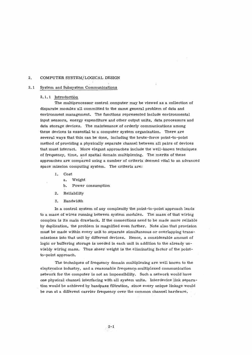
The advanced guidance and control computer system will not be an
amorphous collection of devices and communications networks. Rather, it
will be sectioned along natural and efficient partitioning lines as shown below,
1/O DEV 1/0 DEV 1/0 DEV
Of 1/0 COMM GROUP
1/0 CONT
SptititpithTf7A CENTRAL DATA GROUP
DATA EXEC
MEM'S HDWRPROC'S
COZ/LLLLD INSTR DATA GROUP -INSTR
. MEM'S
The requirements placed on each of the main communications groups shown
will now be explored. | .
2-3
2.1.2 Input-Output Group
2.1.2.1 Hardware Choice Rationale
The input-output communications group is the largest in size. There
are many different types of I/O devices in it, and it physically extends over
the entire vehicle. In addition, the complement of 1/O devices for one mission
are most likely different from those for another,
Therefore, special attention must be paid to flexibility in terms of
expansion and device choice, and to channel weight minimization of this com-
munications group. These would represent the principal selection factors
provided adequate data bandwidth and link reliability can be obtained.
The point-to-point wiring and crossbar approaches are both penalized
by lack of growth potential in this, the most likely-to-grow section. The
frequency multiplexing approach is penalized by the large numberof indi-
vidual devices present in this group, andthe resultant very wide band-~
width requirements. The logical choice for the I/O communications group
is time-multiplexing.
_This choice minimizes the weight of the channel, since only a few wires
need to be distributed throughout the vehicle, These wires and the necessary
multiplexing hardware in each device can be duplicated for added reliability at
what seems to be reasonable cost. This choice also maximizes the growth and
change potential of the I/O network since additional devices can be easily inserted
at any point along the channel, The only real question left is the available band-
width of such a system compared to the required I/O data rate.
The Apollo Guidance Computer has about 250 interface signals. The
fastest sample or control rate in the AGC is the basic interrupt clock rate of
100 times per second. Thus the AGC has a 25-KHz basic 1/O data rate. In
addition to the control loops which can be run at 100 pps, the AGC has a set of
about 30 higher-speed counters some of which can run at 3.2 KHz. This repre-
sents an additional 1/O data-rate requirement of about 100 KHz. The Apollo
computer, therefore, has a peak worst-case aggregate I/O data rate of 125 KHz.
Provision of a 5-MHz I/O time-multiplexed bus in the advanced computer sys-
tem therefore provides for an increase by a factor of 40 over the Apollo data
rates, Realization of a 5-MHz 1/O bus is considered quite feasible.
a74
2.1.2.2 I/O Scheduling Algorithms
There are two principal techniques by which the multiprocessor central '
computing facility can be informed of events by the I/O devices. They are by
periodic I/O status interrogations as initiated by the central facility, or
through "'on demand" service by the central facility as initiated by the 1/O
devices,
In order to accomplish 'on demand" service - the logical equivalent of
I/O interrupt - some portion of the central facility must be permanently
assigned to detection of all service requests, This task naturally falls to the
1/O Controlier group, which one would envision as a buffer and pre-processor
between I/O devices and the central collection of data processors, It must,
however, be capable of sensing and properly responding to simultaneous or
over-lapping service demands. This would require either a separate request
line for every device or some form of time division multiplexing for various
devices to share the I/O controller's attention to one or a few commonlines.
Since the former alternative has already been shown to be impractical in a
Spaceborne computing system, there evidently is little choice as to how to
schedule I/O interactions with the central processors.
It is proposed that the central processor group be able to initiate either
single samples or periodic sampling of the I/O device group, but that control
over the sampling procedure be vested in the I/O Controller. In this way the
1/O bus can be efficiently shared by both the input and output functions.
The I/O Controller would perform input device status interrogations as
scheduled by the central processors and, upon recejving coded responses from
these units, would command data transfers as necessary. The output functions
are readily served in the same way. The 1/O bus thus operates in a two-phase
cycle; with the I/O Controller interrogating or stimulating one or more. of its
satellite devices during the first phase, and receiving or transmitting data or
status indications during the second.
2.1.3 Central Data Group
2.1.8.1 Hardware. Choice Rationale
The central data and control communications group includes the I/O
controller, processors, -data memories and the executive control hardware.
The primary source of traffic in the group is the data interchangebetween
processors and data memories. However, one basic assumption, based on
Apollo experience, is that the typical program runon a spacecraft computer
does not use large data segmerits. In particular, if a processor contains an
internal scratchpad memoryof reasonable size, it will spend a smallfraction .
2-5.
of its time loading and unloading data, and most of its time processing data
contained in its high-speed scratchpad memory. Proper segmentation of
program further reduces the data bandwidth needed in the central data group
by minimizing unnecessary data transfers.
If we assume certain average program parameter values for the space-
borne multiprocessor, the communications bandwidth necessary to sustain
a Single processor can be derived. If the average duration of a job is
2 milliseconds, the average number of data words read from and subsequently
rewritten into memory by a job is 25; and, ifa memory word is 40-50 bits
long, then the required bandwidth per processoris
2A
28
MO
bits/sec = 1,25 megabits/sec.2X10
In order to maintain N processors simultaneously active and computing, the
aggregate bandwidth must exceed (N X 1. 25) megabits/sec,
In addition to the data memory-to-processor interface, the central
communications group must sustain I/O-to-processor, I/O-to-data memory,
and executive hardware interactions, The I/O interactions which filter
through the 1/© controller are encountered at a rate considerably reduced
from the total I/O bus rates. Certainly no more thanin frequent sampling of
1/O device conditions and occasional data transfers occur here. Hence,
1 megabit/second bandwidth is allotted for I/O interactions with processors
and data memories.
The data-rate requirements of the executive control hardware depend
strongly upon the nature of the hardware used, This hardware could range in
complexity from a simple memory identical tothe data memories up toa totally
independent associative processor with its own redundant storage. The more
autonomy that is granted to the executive control hardware, the lower is the
interface data rate needed to maintain it.
The most sophisticated executive hardware requires at least two data
message interchanges with a processor per job executed, These are used to
insert a new job for current or future assignment to a processor, and to
terminate one of the currently running jobs. Additional messages defined else-
where in the report are used to facilitate program restart capability in the
face of hardware failure or electromagnetic interference conditions, The _
minimum required bandwidth for the executive control function per processor
is therefore | , -
10 messages/JobX 50 bits/message_ = 250 Kbits/sec
2x10° seconds/job
2-6
The maximum bandwidth necessary for the simple memory type of
executive hardware depends strongly on the search algorithms used in the
executive program, and on the lengths of job queues in the memory. It is
nevertheless important to estimate the necessary bandwidth.
First, assume that each read or write access by a processor to the
executive memory requires transmission of address and data across the inter-
face. Second, assume some bound on the number of executive memory
accesses required per job from its birth to its death. These are over and
above the 50 data-word accesses previously alloted each job. If 60 executive
memory cycles are required per job to perform the total executive function of
job insertion, real time scheduling, dispatching and termination, then the
necessary bandwidth per job is
60 words/Job X 50 bits/wordSG = 1,5 megabits/sec,2X10 sec/job
This is comparable to the per job (or per processor) bandwidth requirements
for pure data communications. Since all this activity is directed at the execu-
tive mémory hardware, this memory, in order to sustain N processors, must
have a data rate of at least (N X 1.5) megabits/second, equal to the data bus
executive bandwidth.
The nature of executive hardware usage places an additional constraint
on the communications system. One processorat a time reverts to the
executive function while preventing all the other (N-1) processors in the com-
puter from running the executive for an extended period of time. Thus, it is
not possible to achieve bandwidth increases by having a fast memory servicing
N slow channels to the N different processors, by interleaving accesses. The
only possible solution to this cornmunication problem is to provide a fast
channel from the executive memoryto each processor - i.e., a channel whose
data rate is (N X 1.5) megabits/second. Since interleaved (hence simultaneous)
memory accesses are not allowed, the channels cannot simultaneously carry
data to and from more than one processor and the executive memory hardware.
Thus, no performance improvement over an adequate bandwidth time-multi-
plexed channel can be achieved through the use of a crossbar switchor frequency-
multiplexing techniques. .
A similar argument pertains to the processor-to-data~memory inter-
face. The optimum situation in terms of communications efficiency is one in
which all processors are simultaneously exchanging data with physically
separate memory modules, This is the type of situation that a crossbar
switch allows, provided that the data areas required by each processor are
located in separate memory modules, Needless to say, that fortunate arrange-
ment of data is not always achieved, particularly since many programs run in
a spaceborne computer must access common data sets. Generally such com-
mon data must be declared private for the duration of its use by one processor
and is unavailable to others for that time.
Two additional factors pertaining to data-memory usage are created by
the need for ultrareliable data storage in the spaceborne multiprocessor. The
first is the obvious need to duplicate storage of all nonrecoverable data and,
in particular, to do so in physically separate memory modules. This must be
done to guard against the failure of any one memory module preventing the
execution of a vital program, The second factor is more subtle and involves
protection of data in the event of processor failure. This problem and its solu-
tion are explored in depth elsewhere in the report; however, the results in- .
fluence this section. The added factor regarding data transmission is the
requirement that uninterrupted blocks of data be transmitted from the processor
to a data memory. The entire block of data is validated by the processor at
the end of the block thereby informing the memory to accept the whole block.
The memory modules to which the data block is directed are unavailable to
other processors during the block transmission. Therefore, interleaved writing
memory cycles within one memory module for more than one processor are
impossible. This is true for all memory modules which contain redundant
copies of the data segment being updated, since all copies are simultaneously
updated,
The net. result of these restrictions on the use of memory is to reduce
the number of possible independent simultaneous memory operations, and hence
the number of possible independent simultaneous conversations between pro-
cessors and memories. Thus, in neither the executive memory nor the data
memory interface would the capabilities of a crossbar switch be fully utilized.
For example, consider a system with 10 processors and 10°memories, andwith
triply redundant data storage randomly distributed in memory. ‘The probability
of being ableto establish N simultaneous conversations is as follows:
N Pin)L 1.02 ~ 0,21
3 0,024
4-10 0
2-8
The total utijized bandwidth is therefore (1X 1+2%X.21+3%X.024) = 1.492 times
the bandwidth of only one connection. Thus a crossbar. switch which is therore-
tically capable of 10 times the bandwidth of one channel would yield only i.5 times
the performance of one channel. The money spent on the crossbar hardware
would be better spent on raising the bandwidth of a time-multiplexed bus by
the use of byte-parallel techniques. Our goal for the central data groupis,
therefore, a byte-parallel time-multiplexed bus with an aggregate bandwidth of
at least 60 megabits/second.
2.1.3.2 Queuing Statistics
Given sufficient bandwidth, a time-multiplexed bus will adequately serve
the average communication needs of. the central data group. However, there
are other aspects of the problem which have not yet been explored in this report.
In particular, one must examine the extent of system efficiency loss
which is caused by time-multiplexing and also its effects upon system reaction
speed, This has been done by creating a simplified model of processor-data
memory interaction, and simulating the behavior of the central data bus with
this model,
The model selected incorporates the basic characteristics of that time-
multiplexed bus algorithm which grants access to processors (or memories) on
demand. The transmission enable traverses a closed ring of devices, and only
those which have need of the bus when they are enabled cause bus activity. So
long as any device in the ring requires the bus, there is no idle bus time.In the model used, a numberof active processors (Nmax)are given jobs
selected from a random number generator. Thecharacteristics of the jobs are:
1. A computation interval centered around 9 time units (arbitrary)
with a rectangular distribution of widths between 0 and 3.
2. A transmission interval centered around 1 time unit with a rectangu-
lar distribution of widths between 0 and 1.
The Nmax (parameter from run-to-run) processors are arranged in a ring, and
a transmission-enable pulse is inserted into the ring. Ifa processor has com-
pleted its computation interval when it receives the transmission enable, it
immediately beginsits transmission interval and withholds the enable from the
next processor until it has finished transmitting. The proctssor also pulls a
new job from the random job source and begins executing it. Ifa processor
receives the enable while still computing, it immediately passes the enable to
the next processor in the ring. Ifa complete ring passes the enable without any
transmission taking place, the simulation clock advances until some one pro-
cessor isreadytotransmit. That processor immediately receives the enable
and the process continues. |
2-9
The history of each of the enable cycles is recorded - how many pro-
cessors transmitted and how long the enable took to traverse the ring. If no
processors transmitted in a ring pass, the length of the pass is the delay until
some one processor next wants to transmit. The system throughput is also
recorded as the total number of jobs executed per unit time. The average
length of time that a processor is idle is defined as the time between computa-
tion. completion and receipt of the enable pulse. The idle time is recorded for
each processor,
The Data
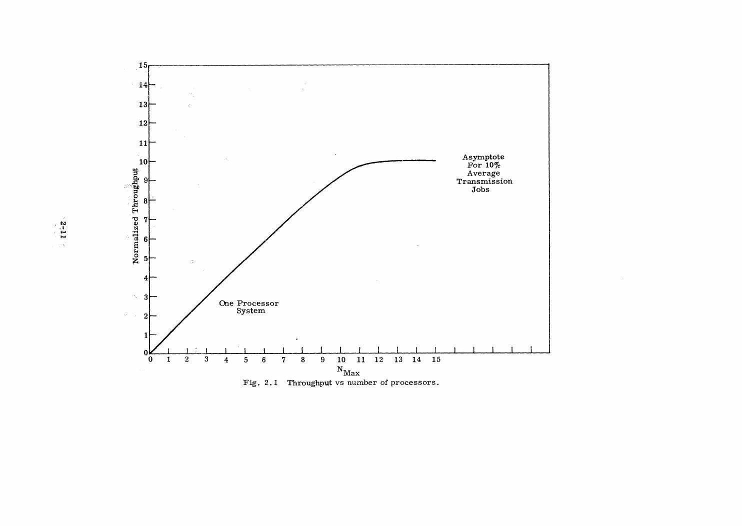
For each value of Nmax (3-15) the simulation ran for 1000 time units.
In this length of time a single processor system would complete an average
of 100 jobs selected from the randomjob generator. It would spend 90%of
its time computing and 10% transmitting. It would never be idle because
there is no competition for the data bus. The throughput curve of the sys-
tem is given in Fig. 2.1. Note that the bus can handle a maximum of
10 simultaneous jobs each of which transmits 10% of the time. Hence,
bus (or memory) bandwidth provides the asymptotic limit on system
throughput.
As the bus load passes full bandwidth utilization, the average idle
time per job goes up sharply as shown in Fig, 2.2.
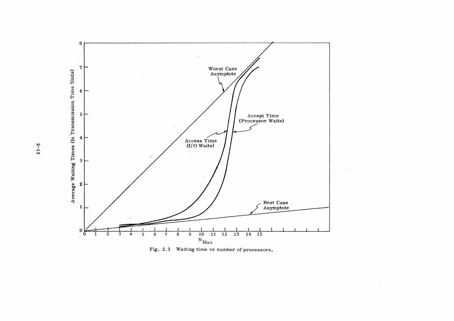
Interrupt Response Time
Another important parameter of the multiprocessor behavioris the
time required to respond either to an internally generated or to an
externally generated immediate job request. The simulation study gives
us some insight into the average interrupt response time.
Let us assume that there are Nmax processors actively computing
and transmitting data to and from E-memory, and also assume that
there is always an idle processor capable of handling the new interrupt
job, If an external stimulus were to arrive at the I/O processor and be
immediately recognized by the I/O processor as a job request, it would
thus immediately appear in the I/O data-bus buffer as a Job Request
message waiting for a transmission enable. The average length of time
the I/O buffer has to wait for the enable to arrive is what is called the
system access time, |
2-10 ©
TT-B-
Normalized
Throughput
15
12h
11;-
10F—-
co. |
One ProcessorSystem ; | 1 I {jf { JtJ Lt |
0 1 2 3 4 5 6 7 8 9 10 41 12 #18 #14 «15Nytax
ax
Fig. 2.1 Throughput vs number of processors.
AsymptoteFor 10%
AverageTransmission
Jobs
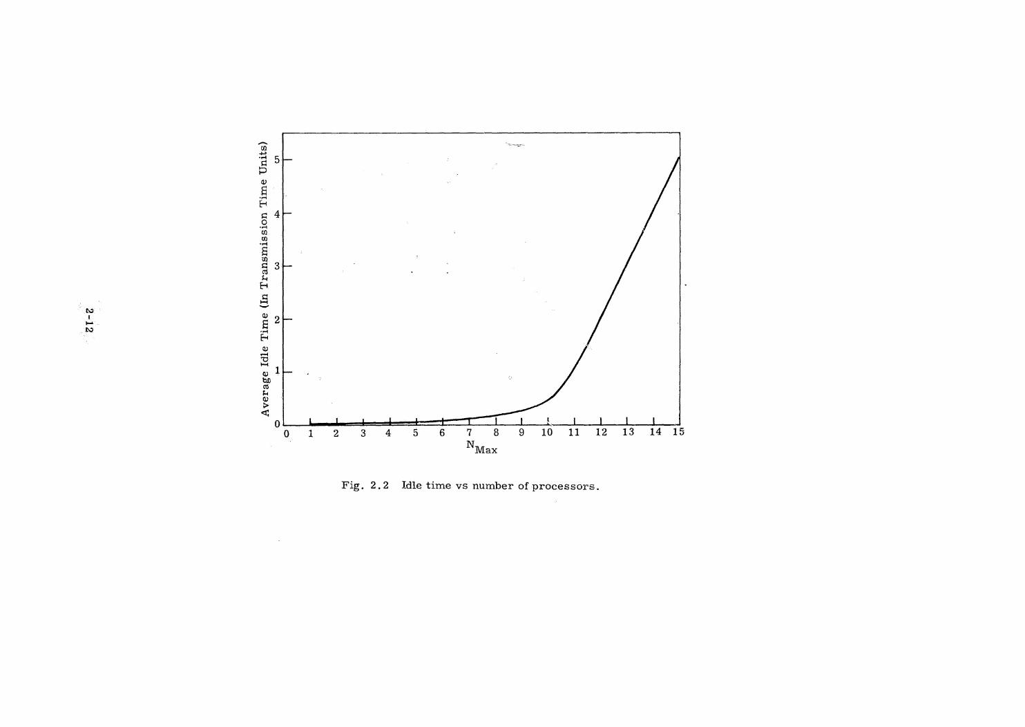
Fig. 2.2 Idle time vs number of processors.
Nuax
Bre
Average
Idle
Time
(InTransmissionTime
Units)
o/
npow
auo
||
|TO
|
10 11 12 13
J14 15
ET-Z
Average
WaitingTimes
(in‘TransmissionTime
Unit
s)
Worst Case
Asymptote
Accept Time(Processor Waits)
=Access Time
_
(I/O Waits)
Best Case
J dssmptote
{ot Lt poy |6 7 & 9 10 11 12 #183 14 #15
Ntax
Fig. 2.3 Waiting time vs number of processors,
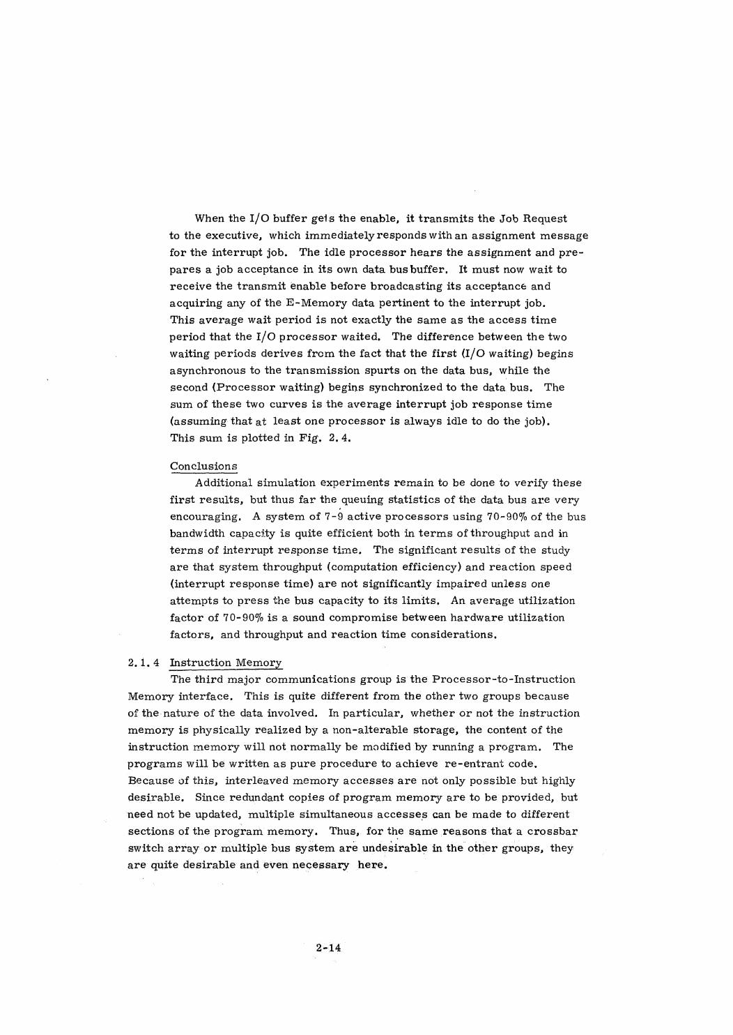
Whenthe I/O buffer gets the enable, it transmits the Job Request
to the executive, which immediately responds with an assignment message
for the interrupt job. The idle processor hears the assignment and pre-
pares a job acceptance in its own data busbuffer, It must now wait to
receive the transmit enable before broadcasting its acceptanceand
acquiring any of the E-Memory data pertinent to the interrupt job.
This average wait period is not exactly the same as the access time
period that the I/O processor waited, The difference between the two
waiting periods derives from the fact that the first (I/O waiting) begins
asynchronous to the transmission spurts on the data bus, while the
second (Processor waiting) begins synchronized to the data bus. The
sum of these two curves is the average interrupt job response time
(assuming that at least one processor is alwaysidle to do the job).
This sum is plotted in Fig. 2.4.
Conclusions
Additional simulation experiments remain to be done to verify these
first results, but thus far the queuing statistics of the data bus are very
encouraging. A system of 7-9 active processors using 70-90% of the bus
bandwidth capacity is quite efficient both in terms of throughput and in
terms of interrupt response time. The significant results of the study
are that system throughput (computation efficiency) and reaction speed
(interrupt response time) are not significantly impaired unless one
attempts to press the bus capacity to its limits, An average utilization
factor of 70-90% is a sound compromise between hardware utilization
factors, and throughput and reaction time considerations.
2.1.4 Instruction Memory
The third major communications group is the Processor-to-Instruction
Memory interface. This is quite different from the other two groups because
of the nature of the data involved. In particular, whether or not the instruction
memory is physically realized by a non-alterable storage, the content of the
instruction memory will not normally be modified by running a program, The
programs will be written as pure procedure to achieve re-entrant code,
Because of this, interleaved memory accesses are not only possible but highly
desirable, Since redundant copies of program memory are to be provided, but
need not be updated, multiple simultaneous accesses can be made to different
sections of the program memory. Thus, for the same reasons that a crossbar
switch array or multiple bus system are undesirable in theother groups, they
are quite desirable and even necessary here.
2-14
St-e
’Average
InterruptResponseTime
15
14
13
12
11
10
WorstCase
Asymptote
Single Data Bus SystemCarries Both Data andJob Messages
Best CaseAsymptote
12
13 14 15
Fig, 2.4 Interrupt time vs number of processors.
The bandwidth requirement of the Instruction Memory-Processor inter-
face is to supply the 66 megabit per second maximum instruction execution rate
of the system, taking sccount of queuing interference, The current éstimate is
100 megabits per second,
The instruction memory group and the communication link must both
have the specified data rate. This is marginally realizable with existing
memory devices, but not with existing links. For both reliability and bandwidth,
it is clear that multiple memories and buses are required.
Considerable design effort must be expended on the tasks of designing
a gracefully degradable multiple-bus system or multiple-crossbar array for
this interface, The desired characteristics are that any processor may use
any bus to interface with any instruction memory. Hence, the failure of one
element only restricts the data flow, but it does not incapacitate any other
unfailed elements.
This is more readily achieved by a multiple-bus system, since each
bus has a total communications capability. A crossbar array has the same
capability, but at a considerably higher ‘component cost, In order to achieve
the desired reliability of interconnection, at least as many crossbar arrays
as time-multiplexed buses would be required. However, each crossbar pro-
vides‘a greater communications bandwidth than a single bus. The numberof
bits that a crossbar must convey in parallel (the width of a byte) is, therefore,
‘less than the number a bus must convey in parallel. This has the effect of
evening up the matching between these two high-speed communications systems;
andadditional study must be performed before a definite choice is possible.
2-16
2.2 Tata Memory
2.2.1 General Structure
2.2.1.1 Modularity
The logical design of the multiprocessor data memory group is
based upon several key requirements. They are:
1. Graceful capacity expansion.
2. Graceful capacity degradation.
3. Absolute data security
The need for data memory capacity expansion is firmly rooted in
the past history of computers in general and the Apollo computer in par-
ticular. As would be expected, the demands upon a computer system
gradually rise to meet its physical limits. Hence the lesson learned is to
be able to expand memory capacity with no impact upon existing programs or
upon their data sets. This goal is most easily achieved by starting with in-
dividual separate memory modules, and with an addressing capability well
in excess of initial needs,
Two avenues of capacity growth are open ~ more modulesor.
larger modules. The former is greatly facilitated by the use of a time-
multiplexed bus for device communications. The act of adding a new
memory module to this bus consists essentially of tapping into a few
existing lines, The latter approach is facilitated by the use of memory-
space segmentation by either fixed or variable length associatively
named pages. The memory space is then addressed by a page name and
a relative address within the page. There is no direct relationship between
a page name and the location of the page within the memory module. Thus,
if the module is enlarged, pages which previously occupied segments of the
smaller module can now just as easily occupy any segment of the larger
module. .
Graceful capacity degradation is the dual of expansion. In order
to be able to compress the data set which existed prior to loss ofa memory
module into the remaining memory modules, the address space of data must
be relocatable. In addition, this relocation should be transparent to the
computer programmer. Again, this capability is greatly facilitated by
segmenting memory into associatively named pages. When data are moved
from one module to another, the relocation is handled automatically; and
the programs which reference the data need not even be informed of its
movement.
2-17
The question of data-memory security is probably the most vital
one relating to the advanced multiprocessor computer. Failures of other
kinds of hardware can be easily circumvented by deleting the malfunctioning
unit from the hardware pool, and reprocessing the supposedly secure data.
Failure of a memory module, however, implies that some data are lost, or
at least suspect. - At best it is unwise to continue processing with such
suspect data, so a way must be provided to eliminate the problem of |
data loss.
The obvious solution is to provide redundant storage in physically
independent modules for vital data sets. No single memory failure can
then destroy all good copies of a vital data set. It remains to be shown
how the duplicate data are maintained and how error conditions are detected
and corrected.
In order to achieve the functions of associative page addressing,
error detection, and data validation and maintenance, the data memory
modules must have a reasonable degree of autonomous logical capability.
In order to retain the desired flexibility for future changes of this logic,
thetechniques of micro-programming will be applied to the data memory
logic as well as to other sections of the multiprocessor computer.
2.2.1.2 Size and Speed |
The basic data-me@mory cycle time would be on the order of cne
microsecond. With the provision of a 32-40-bit data word, the memory
data rate is about 40 megabits/second. This is slightly less than the
data channel capacity of 60 mégabits/second, so that address information
and necessary coding bits can be accommodated on the data bus; and memory
will still be able to operate at its maximum bit rate.
The size of the total data-memory complement is a function
of mission requirements, andcan be readily varied. The increment
of memory capacity is the indiyidual module, so one would like to keep
it fairly small to achieve optimum sizing. On the other hand, considerable
circuitry must be invested per mbdule for page addressing, error control,
and message handling. This would suggest that larger modules would
yield reduced per -bit costs. The ‘current estimates of data-rhemory mod-MS‘S
ule size are 4-16 thousand words of 32-40 bits each. This is subjectto |2
further refinement as the cost parameters are more accurately assessed.
2-18
2.2.2 Page Structure
Each data-memory module is subdivided into a number of data seg-
ments called pages, each of which has a name and a range of physical
addresses within the memory module associated with it. The name of
the page can be associatively linked with the page address base so that
the data within a page can be referenced by either of two addressing schemata.
The first of these is by a module identification plus a base address plus
a relative address. This references a particular word of the data memory
regardless of its page name association.
The second schema utilizes only a page name plus a relative
address within the page. Each data memory module must itself determine
what base address (if any) properly associates with the given page name,
This type of memory reference obtains data which is associated with
a particular page name independent of its physical location within the
memory. it is intended that both of these addressing mechanisms be
available in the multiprocessor.
2.2.2.1 Page Table Addressing
Page name associative addressing is a very useful adjunct to
the multiprocessor computer concept. With it, mission programmers are
relieved of the burden of knowing the mapping of data memory. Some co~
ordination of activity among programmersis still required to allot
memory space efficiently. However, private data storage considerations
within the constraints of these allotments need not be the concern of any
but their user. This is true because variable names as definedby a
programmer can have various scopes of definition. A variable name
defined by a user and its equivalent page name-relative address pair
can be private or global in scope. If private, then other users may adopt
the same variable name for their own programs and will receive different
page name-relative address pairs from the compiler or assembler for
their own use. Hence, the difficult problems of managing a very large
computer program, and the potentially disastrous one of accidental mul-
tiple variable definitions, are alleviated. Variables of global scope,
properly identified as such by the programmer, are commonly translated
for and equally available to all users. The use of this set of variables
must be carefully managed to ensure compatibility among programmers.
However, the exact location of even globally defined data variables
- is not of concernto a programmer, since he may reference it with the page
name associative addressing scheme. Therefore, relocation of any data(by
the whole page) is feasible at any time, and is a function to be performed
dynamically by the executive program. As previously indicated, this ability
isvery useful in guaranteeing both expansion and contraction ofmemory
capacity. | |
2-19
2.2.2.2 Page Table Algorithm
The principal design considerations of an associatively paged data
memory are the achievable characteristics of the association process. How
much time the memory consumes in obtaining a proper page base address when
given a page name is usually its most vital characteristic. This applies most
strongly to systems wherein memory access is granted to a processor for one
memory cycle at a time, with interleaved accesses granted to all requesting
processors. In sucha system, the average data access time is the sum of
the association process time plus the normal memory cycle access time.
Obviously there would be a great penalty paid for a slow association processor
in a typical page-addressed memory system.
However, considering the assumptions of the spaceborne multiprocessor
program structure, this penalty may not be directly applicable to the advanced
computer design. As has been previously mentioned, data transfers to and from
the multiprocessor Data Memories generally take the form of blocks of data
rather than single words. In addition, those blocks are not interruptible for
interleaved memory cycles. Therefore, since a page name-base address
association need be made only for the first word of a block (up to one page in
length), the average memory access time is not merely the sum of the two
access times. It is instead a weighted sum, with the contribution due to page
name lookup being reduced by the average data block length. This gives the
designer of the multiprocessor data memory some latitude in the mechanization
of the page table hardware. The approach favored for realizing the page name
association process takesadvantage of this favorable circumstance,
The storage capacityof each data memory is divided into fourareas, not
equal in size, three of which.are related to page addressing. They are the
main data section, which is itself subdivided into pages, a code entry table,
and an available page list. The fourth section is a data staging area which is
related to data protection and error control. Its use will be discussedlater.
Initially, when the main data section is empty, the code entry table is
also empty. The available page list is preloaded as a bidirectional linked list
of cells, each pointing to a separate vacant main data page. The sequence of
operations which occur when a new page is.assigned to the memory illustrates
the functions of the table and list. The memory logic circuits first transform
the given page name by a pseudo-randomizing algorithm called hash-coding
into an address within the code entry table. This cell is interrogated and, if
empty, it is marked as now occupied, Next, one cell from the available page
list is detached from thatlist and attached by pointer to this codeentry cell.
2-20
The page name being processed(in its original form) is placed within the
detached list cell, thereby establishing a correspondence between the page
name and the page base address initially in that list cell,, These two pieces
of data remainco-resident within the list cell.
Since there are more page names than there are code entry table cells,
there are bound to be occasional instances of different pages names wanting to
enter the memory through the same code entry cell, This situation is handled
by appending the new page name, in its newly acquired list cell, to the existing
list cells with the same hash-code entry. Thus, as the memory Pages become
assigned, lists of page name-page base address pairs are formed from the
appropriate code table entry points. Deletion of a page from the memory
naturally follows the reverse procedure - returning the appropriate list cell
from a code entry list back to the available pagelist.
When such a memory is required to locate a named page within itself,
it applies the identical hash-coding process to the page name as it applied to
insert the page, It then need only search one code entry table list to find the
desired page name. This could be done with a compare-for-equals operation
until the page name match is found or until the list is exhausted unsucessfully,
Alternatively, the individual lists can be keptordered by page name, So that with
a comparison for page name greater than or equals, the search of a list can
be terminated sooner (on the average). Whichever of these is used, page-name
matching or denial thereof will generally occur in less than (1 + N1/N2) or
(1 +N1/2 N2) memory cycles - where N1 is the numberof data pages stored
in the memory, and N2 is the numberof different code entry table cells.
This, of course, requires the hash-coding algorithm to generate an even dis-
tribution of page names.
Advances in the art of LSI technology would enable the realization of
this circuitry and the storage for page name association as a separate assem-
bly from the main data memory. However, as has been shown, we can pro-
ceedwith reasonable expectations from a system in which the storage-for-
pageassociation is a part of the main memory, and has the same cycle time
characteristics.
2.2.2.3 Page Locking
When memory is accessible by several programs running independently,
it is vulnerable to interference not encountered in simplex operation. The
most obvious form of interference is the use of a single register by two pro-
grams to store two independent quantities, as can arise when programs
2-21
independently written are assembled together, This type of interference is
made highly improbahle by the paging mechanism just discussed. A second
kind of interference arises when two independent programs manipulate the
same quantity. It is extremely difficult for the two programs to be cognizant
of each other's actions; and if they are not, then wrong answers can result,
Paging is no help here, since the memory is legitimately accessed by both
programs. A satisfactory soluvion to this problem is the technique of lockout,
which is readily implemented in a paged structure,
The lockout principle is that one or more bits are set aside in thepage
-location table to indicate the status of a page along with its physical location.
These status bits are set to 'lock'’ whenever the page is interrogated by a
processor, There might be exceptions to this when the interrogation does not
influence any results written back. A second processor trying to access the
page will be informed of the lock condition by a message on the Data Bus.
Whether or not the processor is allowed to override the lockout is an unresolved
issue.
The simple lockout procedure just described is inadequate in case of
processorfailure, since a locked page which was supposed to be unlocked by
the processor that locked it will remain locked, Without some identification’
of the locking processor, there is no way to tell which locks should be removed,
For this reason, the lock status bits will identify the processor that lockedit,
which will require four or five bits per entryin the page table,
2.2.3 Data Bus Traffic
The enabling algorithm of the Data Bus will be such that a data memory
access request is answered before any other bus traffic occurs. To implement
the algorithm, the enable wires which pass between multiplexers form separate
rings in the memory group and the processor group, as shown in Fig, 2.5.
The processor-enable ring includes the portion of the I/O buffer devoted
to generating job requests. from external activity. The memory-enable ring
includes the remainder of the I/O buffer, which is concerned with data trans-
mission to and from the environment, The ability to transmit is accorded to
a multiplexer by the occurrence of both of two events. One is the arrival of
an enable signal from the previous multiplexer in a ring, arid the second is the
arrival of another signal to all members of the ring which permits a member of
the ring to have sending access to the bus. The mechanization of the second
enable can be either by a second enable input in each multiplexer or else by
means of transmissions on the bus itself,
2-22-
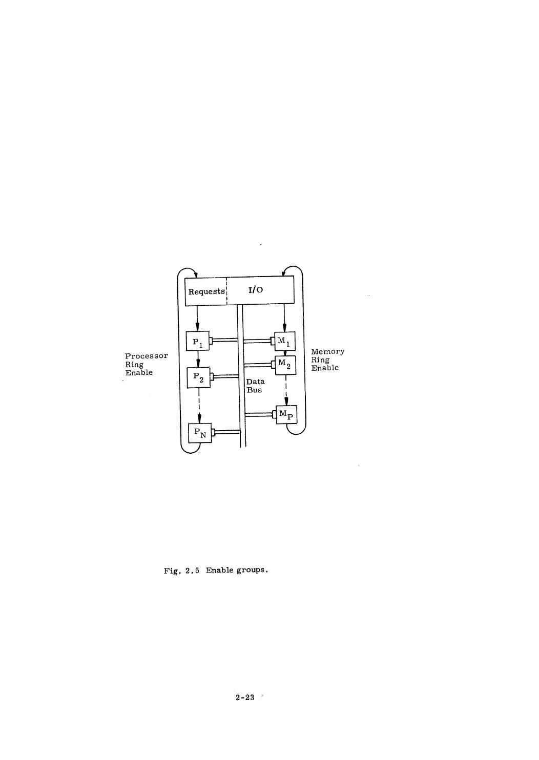
q
|Requests; 1/O|
Pi | MyProcessor
Memory
Ring L M, mine:Enable
nableP, ee
, 2 Data || Bus ,
| 41 oT Mp
Py [-—=+| LS
Fig. 2.5 Enable groups.
2-23

With this arrangement it is €asy to have memory requests answered
promptly and to have job assignments made between any two processors! turns
at transmitting. When a processor makes a memory request it withholds the
enable signal from the next processoruntil its request has been answered
either by data or by lockout denial or until it has been determined that the
request is unanswerable, While the processorring enable is thus immoblilized,
the memory ring enable is passed around so that all of the memory modules
can be consulted for the purpose of answering the request. When a memory
module is ready to answer the request with a data stream, and when it has
received the enable signal, it withholds the enable from the next memory
unit and proceeds to transmit the data stream uninterrupted. In the event ofa
detected error within the memory, the enable is passed on so that another
memory can send the same data stream that the first one was unable to com-
plete. This, of course, assumes multiple storage of data, which is what is
anticipated, At the conclusion of the data stream or of any other response,
the memory sends an enabling signal or message to all processors. The pro-
cessor which had requested the data and whichwas withholding the processor
ring enable now passes on the enable to the next processor. :
To avoid having a master bus control to pass the ring enable from
processors to memories and so around, the rings either pass the ring enable
to one another by hard wire or else every processor and memory must issue
an acknowlegement of its turn on the bus whetheror not it has a message to
issue at that time. The acknowledgement can be a short word and, in fact,
this system is well suited to the use of variable-length messages for the sake
of bus efficiency. The time required to issue acknowledgement messages
for ten processors would presumably be under ten microseconds and would
have a small impact on bus utilization as compared with the hard-wire system,
which has no impact,
Under the acknowledgement scheme, no processor multiplexer would
transmit until receiving a word indicating that a memory transmission is com-
plete. After each memory transmission, therefore, an end-of-stream word
would have to be sent by. the memory unit making the transmission. Similarly,
the processors would send their acknowledgement words after message and data
transmissions to enable the memory ring.
The means by which memory pages are assigned under this regime is a
message from a processor specifying that a page of a given name is requested
to be established in a given memory unit. This message is answered by the
specified memory unit, either confirming or denying the request. If the request
is denied, or if redundant stor(;~e is desired, the processor can request a page
(2-24
in another unit, The requests continue until either the need is satisfied or all
units have been tried without success. In this degraded case some recuperative
measure mustbe taken.
In operation, if an error develops in one memory unit, another memory
unit supplies the desired data, When data are written back, the data go to bothunits. In this way a transient error is overcome. Alarm circuits will distin-
guish transient errors from hard failures and will disable defective pages or
units. When this is done, it will be desirable to create new redundant pages
to replace those lost. This is done by having each program periodically
assess the status of its pages by interrogation messages, similar to the page
assignment messages, which ask if a given page is in a given memory unit.
In this way it can be determined if any pages have been lost; and if so, they can
be reassigned.
2.2.4 Error Control
The design of the data memory units will be strongly influenced by the
need to recover from any system failure. This implies redundant storage of
data vital to continued operation, in fact all data if smooth recovery operation
is desired. It also implies that the memory units be able to detect erroneous
cperation within themselves and shut down partially or wholly, as appropriate.
Beyond this, the memories should be immune to processor errors to the ex-
tent that, ifa processor fails during the time it is writing into the data méem-
ory, the information being overwritten should né\ be lost.Mf
2.2.4.1 Error Detection
Redundant bits for parity checks will be employed in the main memory
and in any memory used for paging and locking. The relative cost of the mem-
ory cells themselves is low enough to permit generous redundancy; the question
remains as to whether it is better to use a Mamming code on a 32- to 40-bit
word or to use a separate parity bit for éach byte. The latter is attractive
from the point of view of byte-by-byte transmission on the Data Bus andof the
cost of implementation. The former has single-error correcting properties
which would reduce the incidence of transient memory output errors.
The remainder of the memory unit will use error detection methods
Similar to those used in the processor. These include replication:of critical
parts, microprogram parity checks, and reasonableness checks on sequencing,: : Co |
A
2-25
2.2.4.2 Error Correction
Whetherer not each memory unit contains error correcting circuits,
the security of data aepends on the ability of the data memory group to maintain
at least two electrically independent copies of all data. However mucherror
correction coding might be used in a single unit, the possibility of massive
failure is too large to try to rely on such means of protection. Loss of power
and broken wires are two modes of failure that are difficult to overcome except
by replication. To achieve overall protection there must be a valid copy of each
testable unit of data, which would be a byte or a word, and the facility for
detecting bad data so it can be replaced. Thus error detection is a key to
graceful degradation in the memory unit just as it is in the processor,
Given that one memory unit can detect its failure and issue a message
to that effect, another memory unit can answer the call for data which the failed
unit had been trying to answer. This system is single-error correcting, but
breaks down if both of two copies are erroneous. The effectiveness would be
much improved if two memory units are able to supplement one another on a
word-by-word basis since it is less probable that the same words in each copy
are in error than different words. One must always bear in mind that memory
errors are not necessarily random, and that what causes an error in one mem-
ory can cause an error in another, Electromagnetic interference is an example
of a means by which nonrandom error combinations are caused, and system
design must take this into account. Thus, whereas it would favor the cause of
error detection to have two memories read data simultaneously withoneverify-
‘ing the Data Bustransmissions of the other, this would be dangerous since the
same electrical accident could easily destroy the same data in two memories.
During writing into memory the danger is similar, yet both memories must
respond to write commands. No adequate answer to this dilemma exists. The
phasing of memory cycles in different units to occur at different times is
clumsy and might reduce reliability rather than increase it. Probably the best
that can be done is to buffer the information to be written securely with repli-
cated registers and/or error correcting codes, Fortunately, if this information
should be lost, it is not irrevocably lost since it can be regenerated by restart-
ing the job that generated it, as describedin the following section. .
2.2.4.3 Over-Write Protection
Since processor errors and transmission errors might not be detected
until after the fact, old data must not be over-written by new data until it can
be verified that the new data transmission is complete and correct, To buffer
2-26 —
all such data and then move them to their proper locations later is unsatis-
factory in that it is time consuming. Otherwise it is an acceptable solution,
since the old data are not disturbed until after the new data have been trans-
mitted to a buffer area in the data memory unit. When this transmission is
declared valid, the data aie moved into their proper storage areas independent-
ly in each of the memory units which are storing it.
To avoid having to move data within the memory unit, a slightly different
strategy may be used, A buffer area is made electrically separate from the
main memory area so that the two can operate simultaneously. Incoming data
are written directly into the proper storage area. Immediately prior to each
word write is a read of that word, as is routinely done in magnetic memories,
and a transfer of theold word to the buffer area. This differs from the simple
buffering scheme in that the old, not the new, information is put in the buffer,
where it can be discarded if the transfer is successful, as is almost always
true. In the infrequent event of a bad transfer, the information in the buffer
is replaced into the storage area, and the job is restarted,
An even simpler storage protection scheme is possible if an entire
page is being written, In this case the information is written into an empty
page. When the transmission is complete and valid, the page table is changed
so that the formerly empty page assumes the designation of the page in question,
and the former page erea is declared empty. A single message from the pro-
cessor will both effect the page table swap and update the executive to advance
the rerun indicator beyond the job segment thus completed. 4a
2-27
2, 3 Instruction Memory
2.3.1 Organization
The instruction memory group supplies processors with program infor-
mation over a set of time-multiplexed buses. To meet the goal of 66 megabits
of instructions executed per second, the bandwidth of the group will have to be
of the order of 100 megabits per second. This can be achieved either by
parallel transmission by bytes, or by using separate buses for each memory,
or both,
The memoryitself is of two classes, One is permanent; the other
volatile, loaded from a bulk storage such as a magnetic tape recorder.
2.3.1.1 Read-Only MemoryIt is anticipated that there will be a category of program information of
the order of several million bits in quantity which will be prepared far enough
in advance of a mission and be of such general utility as to be suitable for
mechanizing as a read-only memory. Operational software, guidance system
programs, display programs and parameters, and nominal mission programs
are examples of such information.
The problem of making a read-only memory highly reliable is less com-
plex than for a read-write memory because no write buffering is needed,
Multiple copies are required because of susceptibility to component failures,
and error detection techniques will be used to determine invalid memory contents
and cause interrogation of alternate copies. MIT/IL is designing such a read-
only memory for the JetPrepulsion Laboratory, and the results are applicable
here using the braid memory concepts previously reported in MIT/IL Reports
R~-498 and E-2092, In addition to parity coding, information is checked by
storing elements of the address in that addressed location and comparing to the
address register, Sense amplifiers are also checked each cycle to see if each
is capableof producing a zero anda one output for the appropriate input.
Densities of a few-million bits per cubic foot are now being obtained
with experimental braidmemories of half-million and one-million bit capacities.
Work is in progress to increase this density several-fold to the order of 15
million bitsper cubic foot. The circuit and mechanical design considerations
are discussed in Chapter 4,
2-28 |
2.3.1.2 Bulk-Loaded Erasable Memory
Because of its high bit density, a bulk storage medium suchas a tape
is the favored candidate for containing most of the mission programs. By
trading off density against redundancy and amplitude it is possible to achieve
very high storage reliability provided a reliable transport mechanism is
available. Mitigating against the very low cost of this medium is its very long
access time. To use a bulk storage in a high-speed machine it is necessary
to buffer its contents in a high-speed memory. The size of the buffer is limited
by its relatively high cost per bit, but it must be at least large enough to con-
tain all programs which will be simultaneously run, plus sufficient redundancy
for reliability considerations, This results in a somewhat complicated cost
function for program memory. The use of read-only memory, which is sub-
stantially more costly per bit than bulk storage but less than buffer memory,
can reduce overall cost if it reduces the size of the buffer. The crossover
point cannot be predicted short of system design, mission specification, . and
software development, For this reason it is especially important that the design
allow physical trading-off between ROM and buffer memory.
Just as the ROM has the specific advantages of fast access and high
dependability, the bulk storage has specific advantages of being open-ended
and being capable of loading a short time before it is separated from its
ground-support equipment. By open-ended is meant that there is no limit to
the number of words which can be accessed other than the bulk memory volume,
The job of allotting buffer space to various bulk memory segments at any
particular mission phase is a challenge to the supporting software. It will be
made more tractable than it otherwise might be by a paging scheme similar
to the one used in the data memory units. Segments of bulk memory will be
stored in pages of buffer memory assigned dynamically by the executive from
an available page list inthe buffer. Instructions are accessed by page num-
ber independent of where they may be located physically in the buffer. This
scheme has the additional benefit of graceful degradation if electrically separate
buffer modules are used in the same way as in the data memory group.
Bulk storage has a second function in the advanced computer, which is
for long-term data storage and buffering. For various reasons, it is indicated
that there should be a separate unit to serve this function. One is that data
storage and buffering operations are incompatiblewith a short access time
for programs inmost media, and a secondis that the reliability requirement is
not as severe in the data application as in the program application due to the
noncriticality of the data so treated, It is felt, for example, that tape transports
2-29
of adequate reliability for this application are probably already in existence.
Still another reason for separation is that it would be logically convenient
to access the data bulk memory via the data memory group rather than the
instruction memory group.
2.3.2 Transmission and Error Control
To meet bandwidth and reliability needs, several paths are needed between
the instruction memory group and the processor group. The particular struc-
ture of these paths will influence the capabilities of the system with regard to
latency and reliability.
Probably the least costly and most straight-forward meansof increasing
bandwidth is to transmit groups of bits (bytes) simultaneously over parallel
paths. Redundant paths may be added for Hamming-coded transmission for
single-error correction as a means of reliability enhancement. This group of
paths would be multiplexed just like a single bus.
A second scheme would more nearly resemble a crossbar switch. Each
unit of the instruction memory group would have its own bus, and each processor
would have access, via a separate multiplexer, to each of these buses, This
provides advantages of average latency reduction and backups for the failure of
a multiplexer, The scheme has the drawbacks of being inflexible and possibly
very costly for a large system.
A third scheme shares a group of buses among processors and memories
by replicating several times the single wire bus with its multiplexers, Whena
processor interrogates the instruction memory group, it places its request
message in all of its multiplexers. The first of these to receive an enable signal
“unloads the others. Each memory unit receives and buffers the request message
until it gets a chance to service it, at which time it so notifies all other memory
units by a message on the same bus. This is a flexible, gracefully degrading
scheme in which bus failure and memory failure are independent,
Which, if any, of these schemes is appropriate is a subject for further
study. To meet bandwidth requirements alone, from three to five paths will
be needed. To meet reliability goals, two or three copies of the ROM and of
the bulk storage and buffer will be needed. © -
/ 2-30
2,4 Processer
2.4.1 Structure
2.4.1.1 General
The goal in processor logical design is to provide performance andflex-
ibility within the limits prescribed by having a modest interface with other sub-
systems and by having a limited proliferation of logic and interconnections
(affecting volume, weight, and power consumption).
The principal sections of the processor are:
Arithmetic Unit,
. scratchpad Memories,
Sequence Generator, and
»o
Do&
Bus Traffic Processors. (See Fig. 2.6).
There are two Scratchpad Memories: one for data, and a smaller one for
instructions, The Bus Traffic Processors are those sections which manage
information transfers between the data and instruction buses and their respec-
tive Scratchpads.
Despite the establishment of performance goals for this study, the actual
performance of the processor will be greater the later it is designed, owing to
technological progress. What is done here is to base the processor's design
upon generally-held forecasts of developments. This design is one which can
meet the stated goals, and which can benefit directly from improvements in
components with no major change in structure,
Two performance criteria are affected by processor design: instruction
repertoire and speed. The latter criterion is the more comprehensive, as it
involves every electronic component, and has a strong inter-relation with com-
ponent count and power consumption, The former criterion is logarithmically
related to word length and, in a microprogrammed machine,linearly related
to the capacity of the sequence generator's read-only memory, an item of
relatively low cost.
Reliability goals are difficult and controversial, Analytic reliability
assessments do not yet reflect all that experience has shown and, therefore,
the availability of a machine cannot be expected to be forecast with any pre-
cision. The graceful degradation concept presumes a statistical independence
among failures, which presumption may not be warranted in anew technology.
2-31
ZE-Z
Data Bus
eeEnable Path —— Data Multiplexer
|
Control Pulse Logic
Read-Only
Memory Sequence Generator
p— —. _. __. —_
Bus Traffic Processor
Data Scratchpad
Memory
eT
| ]
Instruction Scratchpad
Memory
Arithmetic Unit
Instruction Multiplexer->————™_ Enable Path
Instruction Bus
Fig. 2.6 Block Diagram of Basic Processor

It is only by making a unit's mean-time-between-failures (as best it can be
gauged) long compared to mission time, that the aggregate of units can achieve
the extraordinary probability of survival that is required. This may require
the use of masking redundancy. In any event, however long-lasting the unit may
be, the multiprocessor concept still breaks down unless failure detection is
present to a degree that makes the probability of leaving a faulty unit on line
sufficiently small. This detection problem will have a substantial influence
on processor design.
2.4.1.2 Scratchpads
The local data and program storage of the processor are in modestly
sized, relatively fast memories of the type generally referred to as scratch-
pad. The name is derived from the analogy with manual data manipulation.
For instruction memory, it is a misnomer, but the name has an applicable
physical connotation. This application is well-suited for integrated-circuit
flip-flop memories, which are in wide-spread development. (This subject is
enlarged upon in Chapter 3). The memory scratchpad will be supplemented
by the sequence generator's read-only memory (see below), but most instruc-
tions will originate outside the processor and be executed from the instruction
scratchpad.
The data scratchpad is organized in bytes, or short words. The pro-
eessor structure is equipped to handle data in this form throughout, giving it
the ability to handle numbers (words) of different lengths according to need.
Furthermore, the variable-length instruction format proposed for the ACGN
makes byte-addressable memory desirable.
Studies of Apollo guidance programs indicate that demand for data stor-
age is polarized around two lengths, a floating-point word of about fifty bits
(roughly 40 mantissa and 10 exponent) and a flag or single bit, To suit the
demandsof floating-point hardware, it is desirable to makethe length of a byte
an integral power of two bits; and to facilitate the packing of byte data, itis
desirable to have an integral power of two bytes per word, The most desirable
word lengths would then be 32 or 64 bits which could be arranged in four or
eight bytes of eight bits. Unfortunately, thirty-two bits is insufficient to con-
tain floating point numbers with any useful accuracy and sixty-four bits is
somewhat extravagant,
Another factor in choosing byte length is the address range of the scratch-
pad itself. In this regard eight bits is marginal and ten bits generous if word
addressing is used. In either case, the mantissa for floating point words would
be 40 bits, i.e., five or four bytesrespectively.
2-33
As in all memories, if a failure affects a single bit position and no
others, an error-correcting code can maskthe failure. Thus a scratchpad
memory of eight or ten useful bits can be made to survive a component failure
if it is so organized that memory cells.in the same component occupy the same
bit position in different words. Four additional bits would be needed for error
correction of a single failure, and one mor bit (parity) would provide detection
of a second failure, Whether or not to employ this form of design is not an
obvious choice. Its advantage is clear; it provides survival in the event of a
single failure. Its disadvantage is cost; and,in addition, the question arises
as to whether a unit encumbered by a single failure would be desirable to have
on line.
The numberof bytes in the data memory must be sufficient to allow the
assembly, dispatch and manipulation of data. It is therefore desirable that
several pages of common memory, and preferably more, should fit in the
processor's data scratchpad. Since there are physical constraints on scratch-
pad size and paging electronics in common memory, the page size and hence the
scratchpad size will be dependent on implementation for several reasons, At
a minimum, several thousand bits would be required.
The instruction scratchpad memory is considerably smaller than the
data scratchpad. Instruction fetches from the common instruction memory are
planned to be as many as 256 bits at a time, and the scratchpad must be large
enough to contain twoor more of these blocks. The memory is byte-organized,
like the data scratchpad, permitting easy access to variable-length instructions.
2.4.1.3 Sequence Generator
A microprogram form of sequence generator is deemed best for this
processor, It offers flexibility and compactness at a possible speed sacrifice.
Instruction microprograms are stored in a read-only memory, highly efficient
of size and cost per bit. There is virtually no limit to the instruction complexity
that can be incorporated this way. Error control within this read-only memory
is implemented by single- or double-error correction coding.
The organization of the sequency generator will be such that contents
of the read-only memory can be interpreted as microprogram or as program;
thus, each processor can have its own repository of certain frequently-used
programs. Some complex operations generally handled by program subroutines
in present computers may be handled in this. processor either by subroutine,
by long microprograms, or by a combination, according to demands on speed
and storage efficiency. Such operations would include major arithmetic opera-
tions (vector and matrix arithmetic) and routines for fetching and storing Gata
in the common memory.
2.4.1.4 Arithmetic Unit
The arithmetic unit will provide facilities for the standard combinatorial
operations on words: addition, subtraction, multiplication, division, shifting,
normalizing, logical product, logical sum, and logical inversion. These
operations will be implemented a byte at a time with provision for multi-byte
wordsto be processed within the mircoprogram structure. In addition,
floating point arithmeticwill be part of the instruction repertoire, and will
use hardwarein the arithmetic unit appropriate to its execution.
To achieve the goals discussed in Chapter i, the speed of the arithmetic
unit will be such as to permit a full-precision addition in one or two micro-
seconds, and a full-precision multiplication in five to ten. To realize this with
a parallel register organization is not difficult. On the other hand, since a
serial organization minimizés interconnectionsand simplifies testing and
checking, it is of some interest to determine whether sufficiently fast shifting
and adding circuits are available. At present, the semiconductor industry
produces high-density shift registers too slow for this purpose. The future
holds much promise for higher speeds, however, and the advantagesof serial
operation make it attractive enough to use for the processor design. A serial
arithmetic unit is further discussed in Chapter 3,
2.4.1.5 Bus Traffic Processing
An important facet of processor design is the means by which the ex-
change of information with other units is reconciled with normal operation.
This is done by sections of logic which interface with the multiplexer, the
sequence generator, and the scratchpad memcries.
Since transmission rates of tens-of-megabits per second are expected,
it follows that several bytes per microsecond maybe transferred between
scratchpad and multiplexer. Three possibilities for handling this transfer are
to do. it in normal mode, in interrupt mode, or by cycle stealing. For message
and data memory transfer, one of the first two would be appropriate. As
presently envisioned, the multiprocessor structure is such as to make it possible
for each processor to idle and scan the multiplexer whenever a relevant message
is expected. This being true, no interrupt is required, Ifgreater flexibility
‘is required, interruption of p*ogram for message handling would be called for.
This would require either a very quick interrupt, with a response time of less
than one instruction, or else a buffer store on the multiplexer. The present
processor design concept has no interrupt, for the sake of design simplicity.
This is not to deny the possibility of its eventual inclusion, however.
In the case of instruction traffic, the destination of the instruction
information is not in the processor's addressable data area, and transfer
occurs during general program execution. Cycle stealing is an appropriate
means for moving information into the instruction scratchpad.
The bus traffic processing sections have the capability of recognizing
bus information, i.e., distinguishing between relevant and irrelevant messages,
data, and instruction. Moreover, they have the capability of verifying that a
transmission from the processor appears correctly on the bus.
2.4.2 Instruction Execution
In this section, methods for minimizing the length of instructions are
discussed, Although it is doubtless clear that such efficiency is worthwile,
perhaps it is worth emphasizing that, in addition to the saving of bits of physical
memory, a reduction in the length of the average instruction increases execu-
tion speed both by increasing the average *umbher of instructions per fetch and
by increasing the probability that the target oi a branch instruction is already
contained in the program buffer.
2.4.2.1 Instruction Formats
Consider the two most common types of instruction, referred to as
unary and binary, respectively, because of the number of operands utilized:
f(B) ——_» A
4B, C)-——+ A
If one or more address fields could be deleted from these instructions,
and if, on the average,the saving due to the deletion is greater than the extra
space required to store indicator bits which describe the presence or absence
of address fields, the result is a net improvement,
The two means proposed to effect this saving are:
1. Implementation of scratchpad memory in such a way that it acts
28 a pushdown stack; and «
2. Omission of the (only) operand address field or first operand
addressfield if that operand location is identical to the result or
sink location. : |
Assumethat with each instruction there is an associated group of hits
called the instruction format code (IFC). Then, if the IFC specified the type
of addressing, it is possible, for example, to have a binary instruction with
no explicit address, or with 1, 2, or 3 addresses, as appropriate.
The functioning of the pushdown stack is as follows: When an item is
"pyushed down", the behavior is as though information already in the stack
were moved to the next location down, and the new entry added at the top.
When an item is taken from the stack, the top item is delivered as the operand,
and the data remaining in the stack is effectively "pushed up" one location.
Typical implementations of pushdown stacks do not actually move the stored
information up and down, but function by using a register which contains the
location, say, of the "top" entry in the stack, and perhaps other registers
which specify stack boundaries, for checking purposes.
The logical efficiency of the pushdown mechanism may be demonstrated
by an example, Consider first an algorithm to calculate one root of a quadratic
equation:
1/2(-B + (B* - 4 ac)!/4)/2a—>x
Using Ti - T3 as temporary storage locations, this might be programmed as
follows, using only explicit addresses:
1. AXTWO —+T1 2A2, AXFOUR -——+T2 an3. T2xc —» T2 4AC4, SQUARE (B)-——+ T3 B?5. T3-T2 —»T2 B? - 4AC6. SQRT(T2) ——T2 fo7 T2-B —» T2 numerator
8. T2 TL ~~»X done
In this example, note that addresses have been written in 22 places, Now
examine the same algorithm coded with specification of pushup and pushdown
(*) instead of actual addresses, The occurrence of * on the left side of the
replacement arrow indicatesa "pushup" operation, while its occurrence on
the right side indicates a "pushdown". Each program step above proceeds
from left to right. |
(2-37.
1 AXTWO ——>* 2A
2, AXFOUR ——»-* 4A3. CX* ——> 4AC4, SQUARE (B)——> * B’5. ok —— B? - 4Ac6. SQRT (*) —=*7 **-B —s * numerator
8, kr —»X done
The saving is evident, since only eight addresses are explicitly written.
The "implicit sink" instruction form can also save space, as in the
coding for
X + lex
which requires the address of X to be specified twice unless "implicit sink"
is specified,
The numberof bits required to specify the instruction format may be
determined by listing the possible cases:
f{(B) —.A f(A) —~*
f (A) —» A .
f£(*) —= A 7) i
f (B,C) —> A f (A, B)—~ *
f (A,B) —» A
f(*,B) —»~ A f (*, A)——> *
£(B,*) —» A f (A, *)—= *
f (A,*) —~ A
f (%, *) — A f (, 6) ——e ok
_ Since there are only fifteen formats, a four-bit prefix is sufficient to specify
which addresses are absent from the instruction, and why.
2.4.2.2 Addressing
Because of the three types of memory, three types or ranges of
addresses are require, From the programming standpoint it would be
desirable that the entire range of possible addresses be divided into three
regions. The lowest-numbered addresses might refer to scratchpad, for
example, the next region to general erasable,.and the highest addresses
to program memory. Note that low-range addresses do not uniquely
2-38
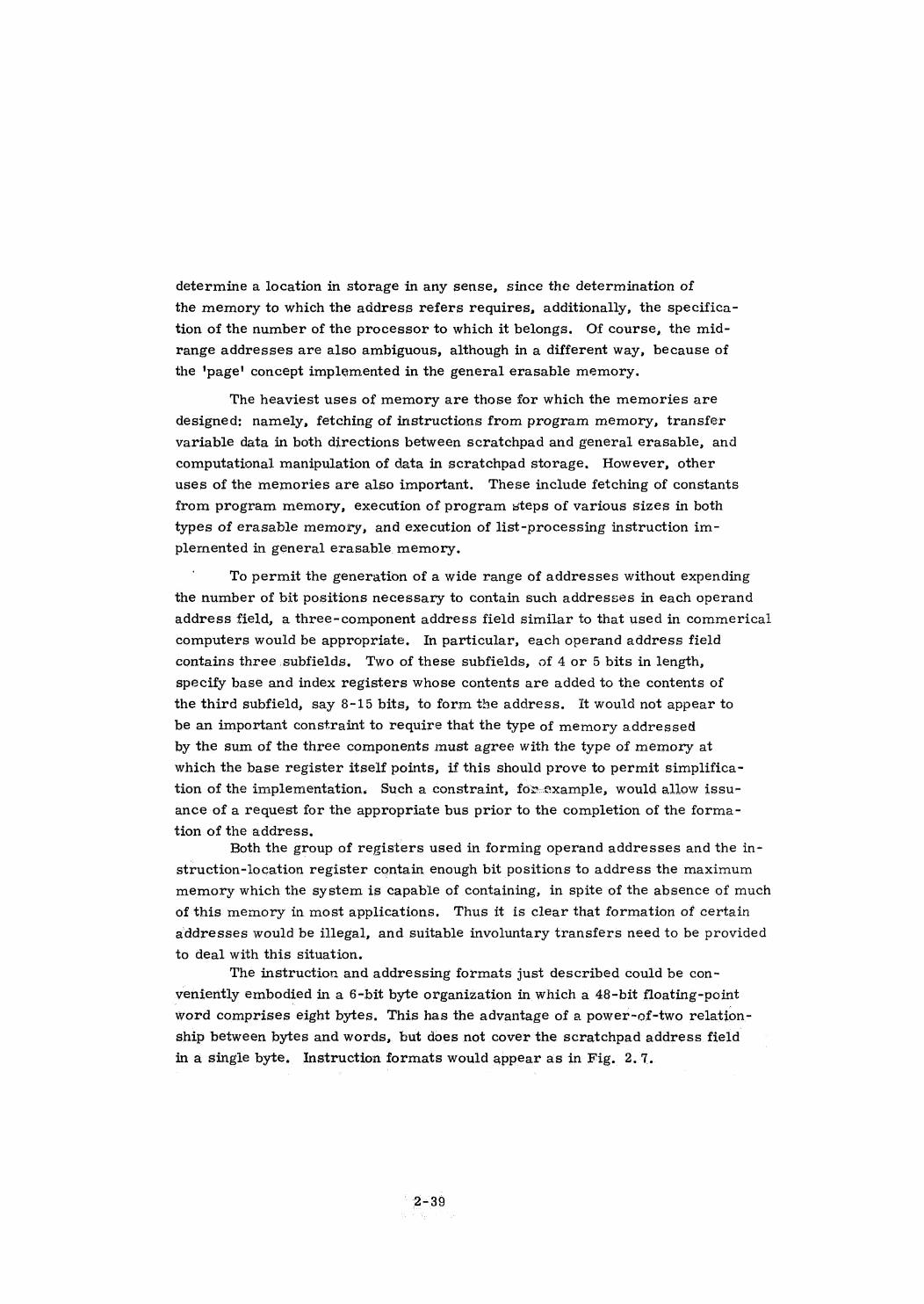
determine a location in storage in any sense, since the determination of
the memory to which the address refers requires, additionally, the specifica-
tion of the numberof the processor to which it belongs. Of course, the mid-
range addresses are also ambiguous, although in a different way, because of
the 'page' concept implemented in the general erasable memory.
The heaviest uses of memory are those for which the memories are
designed: namely, fetching of instructions from program memory, transfer
variable data in both directions between scratchpad and general erasable, and
computational manipulation of data in scratchpad storage. However, other
uses of the memories are also important. These include fetching of constants
from program memory, execution of program steps of various sizes in both
types of erasable memory, and execution of list-processing instruction im-
plernented in general erasable memory.
To permit the generation of a wide range of addresses without expending
the numberof bit positions necessary to contain such addresses in each operand
address field, a three-component address field similar to that used in commerical
computers would be appropriate. In particular, each operand address field
contains three subfields. Two of these subfields, of 4 or 5 bits in length,
specify base and index registers whose contents are added to the contents of
the third subfield, say 8-15 bits, to form the address. It would not appear to
be an important constraint to require that the type of memory addressed
by the sum of the three components must agree with the type of memory at
which the base register itself points, if this should prove to permit simplifica-
tion of the implementation. Such a constraint, fox-example, would allow issu-
ance of a request for the appropriate bus prior to the completion of the forma-
tion of the address,
Both the group of registers used in forming operand addresses and the in-
struction-location register contain enough bit positiens to address the maximum
memory which the system is capable of containing, in spite of the absence of much
of this memory in most applications. Thus it is clear that formation of certain
addresses would be illegal, and suitable involuntary transfers need to be provided
to deal with this situation.
The instruction and addressing formats just described could be con-~
veniently embodied in a 6-bit byte organization in which a 48-bit floating-point
word comprises eight bytes. This has the advantage of a power-ef-two relation-
ship between bytes and words, but does not cover the scratchpad address field
in a single byte. Instruction formats would appear as in Fig. 2. qT.
» 2-39
oF-e
Field | [TFC OP a B, I, D, Bo
No, of Bits 4 8 4 4 10
Byte No. I 2 3 4 5
Fig. 2. 7 Instruction formats for six-bit byte, three-fieldaddress organization.
This format for addresses wouldpermit either byte- or word-organized
addressing. The disadvantage of byte addressing is that the 10-bit displace-
ment can only reference within blocks of 128 words. By addressing words,
blocks of 1024 words could be accessed without switching base registers. How-
ever, byte indications would have to be given separately where applicable
(branches, logical operatons with immediate data, etc.). To conveniently
access data of varying length in a byte machine, floating index registers might
be implemented. These would shift the value in the index register left accord-
ing to the type of data implied by the instruction before actually adding it into
the address. Thus, one might access successive words in a table merely by
modifying an index register by 1 each time.
2.4.2.3 Processor-Local Addressing
An alternative addressing organization economizes on the length of
instruction words at the expense of programming convenience, and possibly
speed, In this approach, the processor can directly address only what is in
its scratchpad memory. Access to the common data memory is made by first
explicitly commanding a transfer of data to the processor's. scratchpad,
This somewhat unconventional scheme is éxplored in this section. No commit-
ment is made herein as to whether it is more or less desirable than the scheme
previously described, since it is felt that the subject needs further investigation
before a choice can be made,
2.4,2.3.1 Program Memory Addressing and Instruction Handling by Processor
2.4. 2.3.1.1 Review of Instruction Handling
Program words for the entire multiprocessor system are kept ina
central Instruction Memory. Small blocks of program are transferred over
the Instruction Bus from the Instruction Memory into the Program Store in
individual processors. Actual execution of program takes place from the Pro-
cessor Program Store. The transfer takes place in response to a Program
Read Message issued by a processor,
A convenient approach involves transfer of a block of program words
from the Main Instruction Memory to the Processor Program Store for each
Program Read Message. The larger the number of words in the program
block, the fewerthenumber of message words that must be put on the bus
to obtain a given:number of program words, On the other hand, the larger
the number of words in theprogram block, the more likely that not all program
words transferred will actually be executed before a transfer of control out of
the block is required, | .
(2-41

It would be advantageous te employ subaddresses in the instructions
themselves wherever possible. This reduces the numberof bits that must
be provided in the Main Program Memory, that must be transferred over
the bus, and that must be stored in the Processor Program Store.
2,.4,2.3,1.2 Description of Proposed System
2.4.2.3.1.2.1 Addressing Scheme
Assume the Processor Program Store holds N bytes of program. A
Program Read Message issued by the processor will cause a block of N bytes
to be transferred from the Main Instruction Memory to the Processor Pro-
gram Store. The Main Instruction Memory is divided into N-byte blocks.
Groups of these N-byte blocks form Programs. Therefore, any program word
in the Muin Instruction Memory can be referenced by a Program Number,
Block Number, and Relative Address within the Block. Addressing within a
Block is relative to the first address in that Block. Block Numberswithin a
Program are relative to the first Block in that Program.
Program words consist of a variable numberof bytes. A field at the
beginning of each program word will be set aside to indicate the numberof
bytes making up that program word.
Associated with the Processor Program Store, there is an ID Register
which contains the Program Number and the Block Numberof the current con-
tents of the Processor Program Store.
Reference parts of instructions that refer within their Block require
only a Relative Address. Reference parts of instructions that refer within
their Program but outside their Block require a Block Number and a Relative
Address. (The ID Register contains the current Program Number.) Reference
parts of instructions that refer outside their Program require a Program Num-
ber, Block Number, and Relative Address.
2.4.2.3.1.2.2 Out-of-Block References
At execution time, the basic unit of program is the Block. Before
running, a Block of program is read from the Main Instruction Memory into
the Processor Program Store. After execution of the last instruction in a
Block, the processor composes and issues a Program Read Message for the
next Block in sequence, causing it to be read into the Processor Program Store.
if there is a "transfer control" type of reference out of the current
block, the processor composes and issues a Program Read Message for the
new Block, causing it to be read into the Processor Program Store, Execution
is begun at the referenced Relative Address. :
2-42

If there is a single word ''data fetch" type of reference to a Blovk of
Instruction Memory that is not currently in the Processor Program Store, the
entire new Block is not read, The processor composes and issues a Program
Read Message only for the referenced word, causing it to be read into the
Processor's Accumulator. (For block data fetch, see next section.)
2.4.2,3.1.2.3 Program Read Messages
Program Read Messages are of two types: those which cause a Block
of Main Instruction Memory to be read, and those which cause a single word
of Main Instruction Memory to be read. The former requires the Program
Number and the Block Number of the desired Block; the latter requires the
Program Number, the Block Number, and the Relative Address of the desired
word,
Program Read Messages can be written explicitly into the program or
can be composed and issued by the processor because of an out-of-block
reference, as discussed in the previous section. In the latter case, the
Processor uses the Program Number found in the ID Register if the out-of-~
block reference is within the current Program. It would be useful to have a
data-read message for transferring blocks of constants from the Main Instruc-
tion Memory directly into the Processor Data Scratchpad. This message
would require the Program Number and Block Numberof the desired block, and
also the address of the first register in the Scratchpad into which the first word
of data should be placed.
2.4.2.3.1.2.4 Addressing Within Processor
For any word in the Main Instruction Memory, the relative address
(within the block) of the register from which the word is read is the same as
the address of the register into which the word is placed in the Processor
Program Store, Thus it is possible to transfer a block of program from the
Main Instruction Memory to the Processor Program Store and execute it
directly without performingaddress modification,
Addresses for the Processor Program Store (loaded from Main
Instruction Memory) and for the Processor Data Scratchpad (loaded from
Main Data Memory) do not overlap. Program instructions can refer to either
uniquely.
The memory layout is illustrated in Fig. 2.8, and the four classes of
address reference are shown in Fig, 2.9. — ,
» 2-43 >
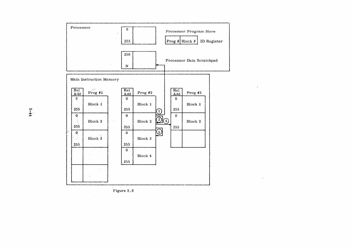
b-Z
Processor 0Processor Program Store
255 Prog #| Block #1 ID Register
256
Processor Daia Scratchpad
N
Main Instruction Memory
Rel a Rel RelAdd Prog #1 Add Prog #2 Add Prog #3
0 0 0Block 1 Block 1 Block 1
255 255 ID 255
0, 0 — 0 |
| | Block 2 | Block 2 Ala Block 2| 255 255 2550 / 0 @)
“o. 1 Block 3 Block 3255 255 |
. 0
Block 4
‘1.255
Figure 2.8
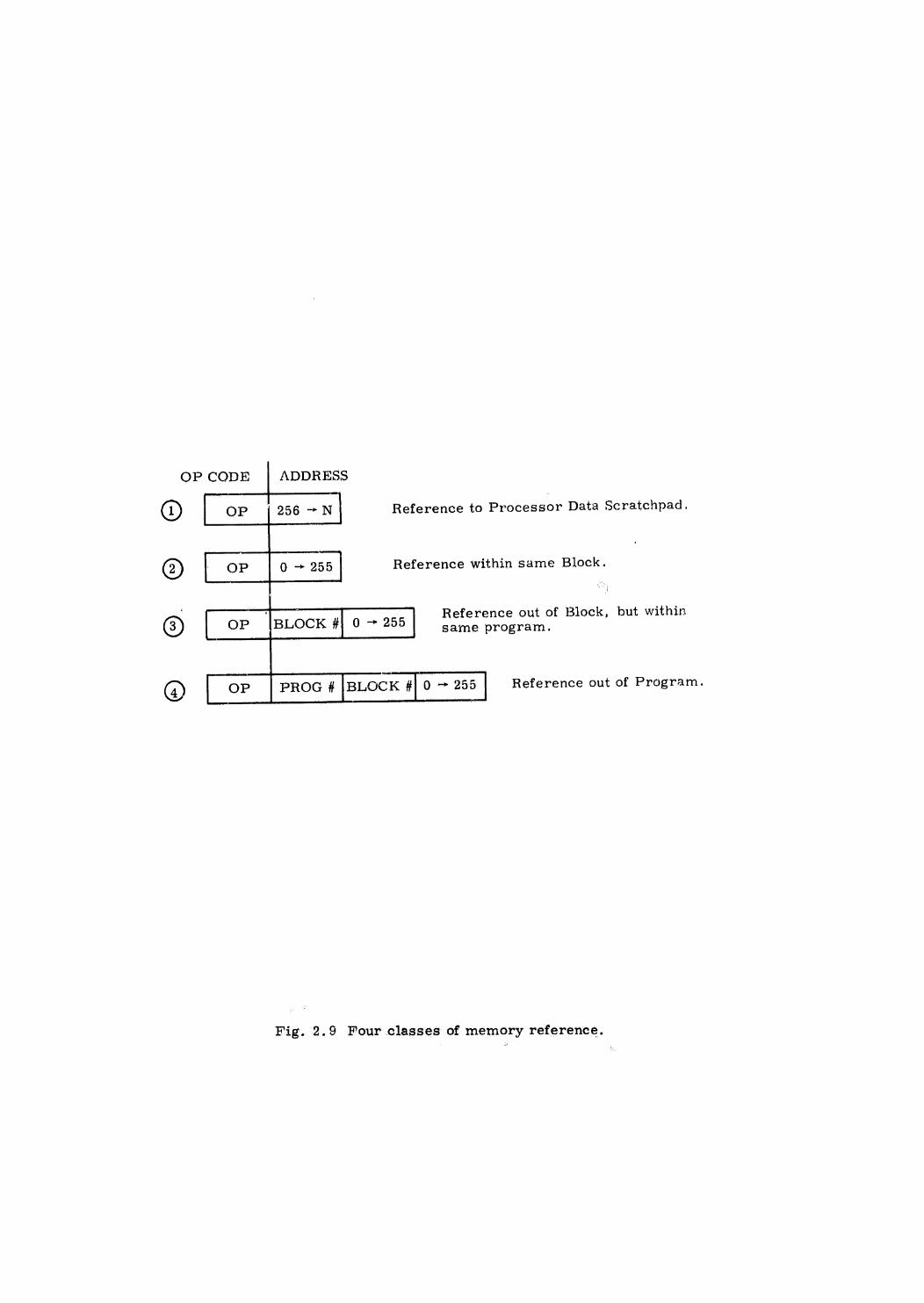
OP CODE ADDRESS
OP 256 -~ N Reference to Processor Data Scratchpad.
OP 0 ~ 255 Reference within same Block.
op |BLOCK #| 0 > 255 Beeeeerom. Block, but within
OP PROG # |BLOCK #] 0 > 255 Reference out of Program.
©©
©©
Fig. 2.9 Pour classes of memory reference.
2.4.2.3.1.4 Indexing
Indexed instructions exist in the Main Instruction Memory with the
shortest form of reference address as possible, just as non-indexed instruc-
tions. Since the indexing cperation may cause the’reference to cross block
boundaries, a complete address (Program Number, Block Number, and
Relative Address) is required at execution time for the reference address of
indexed instructions. If the reference address is not complete, the processor
will build up a complete address at execution time by referring to the current
block ID Register for the absent fields,
After indexing, it is desirable to refer to the current block JD Register
to decide if a new block must be read in or if the final reference is to the
current block. This saves reading in a new block needlessly.
2.4.2.3.1.5 Program Modification
Since the Processor Program Store is an alterable memory, a program
can modify itself at execution time. This is of limited use since any modifications
made to program in the Processor Program Store will be lost for all time when
a new block of program is readin. Any subsequent read of the block of program
that was modified will obtain the unmodified copy from the Mair Program. Mem-
ory. Error control would be complicated by such operations.
2.4.2.3,1.6 Muiti-Block Processor Program Store
2.4.2,3.1.6,1 Two-Block System
A useful extension of the proposed processor organization would be to
add a second block to.the Processor Program Store. One Program Store con-
tains the block of program currently being executed; the other, the last block
of program that was executed before the current block. An ID Register is
needed for each block in the Processor Program Store. When reference is
made outside the block currently being executed, the other block's IDRegister
is used to determine if the yeferenced block of program is already in the other
section of the Processor Program Store. Only if the referenced block of pro-
gram is not already present in the Processor Program Store would it be necessary
to read from the Main Instruction Memory. Whenever a new block of program
is read from the Main Instruction Memory, it is written over the block in the ..
. Processor ProgramStore from which program is not currently being executed.
. Addressing’ for both blocks in the Processor Program Store isthe same
as the relative addressing within a block in the Maza Instruction Memory. ,Thus,
program can be executed from either block in the Processor Program Store
‘without address’ modification. .
2-46
The two-block system decreases the number of program block.transfers
from the Main Instruction Memory in situations in which program in one block
calls program in another block which returns to the first. If this occurs ina
loop, so much greater the saving. ©
_2.4,2,3,1.6,2 Three-Block System
A further extension of the processor organization would be to adda
third block to the Processor Program Store. One block contains the block of
program currently being executed (current); another, the blockof program
that was executed just before the current block (last); the third, the block of
program that was executed just before these two (oldest),
Whena transfer of control is made to a new block of program, the
block is read from the Main Instruction Memory into the oldest block and this
block is marked as "current", The block from which the transfer of control was
made is marked as "last", The block that was "last'' becomes "oldest", Of
course, whenever a reference is made outside the block currently being executed,
the ID Registers for the other two blocks in the Processor Program Store are
consulted to determine if the referenced block of program is already in the
processor, If so, no new block is read, The block to which transfer of control
is made is marked as "current''", The block from which transfer of control is
made is marked as "last", The third block is marked as "oldest" (it may
already have this status).
Another approach for the three-block system would beto use one block
. for "current", one for "last", and the third for a guess of "next",
2, 4,.2.3,1.7 Alternative Considered to Proposed System’
Another possible system has no predetermined, fixed blocks withinthe Main Instruction Memory. When a transfer of control is made out of the
current contents of the Processor Program Store, a block of 256 bytes beginning
with the referenced wordis transfeitred from the Main Instruction Memory. If
program is executed sequertially, all instructions in the transferred block will
be executed. This resolves one problem of the predetermined, fixed-block system
_ where transfer of control to a word nearthe end of a block causes many trans-
ferred words to be wasted,
Since the start of any block to be transferred from the Main Instruction
Memory is not knowt in advance, it is not possible to supply addresses relative
to the start of their block. Therefore, addresses must be modified at execution
time by subtracting out the address of the first word in the block transferred to
247
the Processor Program Store. No such modification is required in the pre-
determined, fixed-block system. Also, more bits are required for address
references within current block then in the predetermined, fixed-block system.
In addi:.on, a single predetermined byte for column parity checking cannot
be used, This alternative scheme is deemed to be less satisfactory than the
fixed-block scheme,
2.4,.2.3,2 Erasable Data Handling by Processor
2.4.2,3.2.1 General Description
Data words for the entire multiprocessor system are kept in a central
Erasable Memory. Since the Main Data Memory is divided into pages of equal
length, a page number and relative address within the page are required to
reference. any word in the memory. The page numbers used by all parts of
the system outside the Main Data Memory do not necessarily refer to the actual
physical pages in the memory. The transformation between the page numbers
used for communication with the Memory andthe actual physical pages in the
Memory is pérformed by theMemory System. Data are transferred over the
Data Bus from the Main Data Memory into the Data Scratchpad in individual
processors, Actual manipulation of data takes place from the Processor Data
Scratchpad. The transfer takes place in response to a Data Read Message
issued by a processor,
2.4,2,3.2.2 Scratchpad Function
The Processor Data Scratchpad is used as a buffer for Main Data
Memory data, as well as storage for temporary results. A typical job issues
a Data Read Message to transfer a block of data from the Main Data Memory
(not necessarily all from the same page) into its Scratchpad, performsits
computations referring to Processor Scratchpad, and issues a Data Store
Message to transfer results back into the Main Data Memory. It is desirable
to transfer several words of data with a single read or store message, in
order to reduce the number of message words that must be put on the bus to
transfer a given number of data words. Notice that program instructions do not
refer to the Main Data Memory, but only to the Processor Scratchpad.
2.4.2.3.2.3 Erasable Data Read and Store Messages
Read andStore Messages involvingtransfer of data between the Main
Data Memory and an individual processor's Scratchpad Memory appear
2946
explicitly in the program executed by that processor. These messages
contain the following information:
Page Number in Main Data Memory.
Relative Address within page of first referenced word.
Number of consecutive words of data.
Processor Scratchpad Address corresponding to the first word of data.
The Processor Scratchpad Address specifies into which Processor Scratchpad
locations data will be placed by a Read Message or from which Processo?:
Scratchpad locations data will be obtained by a Store Message.
2.4.2.3.2.4 Consequences of Read and Store Message Format
Since program instructions do not refer to the Main Data Memory but
only to the Processor Scratchpad, the address references needed require
fewer bits. This reduces the numberof bits that must be provided in the
Main Instruction Memory, that must be transferred over the bus, and that
must be stored in the Processor Program Store.
For any word in the Main Data Memory, the relative address within
the page of the register from which it is read need bear no relation to the
address of the register into which it is placed in the Processor Scratchpad.
A similar statement applies to storing from the Processor Scratchpad into
the Main Data Memory. This flexibility is a result of being able to specify
any Scratchpad Address in Read and Store Messages, Furthermore, data
from different pages in the Main Data Memory can be mixed in the Processor
Scratchpad. . .
Portions of the Processor Scratchpad containing data no longer required
by the program running on the processor can be re-used to receive new data
brought in by subsequent read messages,
2.4.2.3,.2.5 Implication on Programming
2.4.2.3.2.5,1 Basic Language Programming
Symbolic names of pages in the Main Data Memory are declared to the
assembler, The assembler assigns a page identifier number tothe page name.
These page numbers bear no relation to pages in the actual memory. They
need only be distinguishable from all other pageidentifier numbers. Main
Data Memory register symbols are declared to the assembler to be within
specific pages already declared. The assembler assigns a relative address
within the appropriate page to each of theseregister symbols in the order of
declaration. ,

Processor Scratchpad register symbols are declared to:the assembler.
These are in effect only for the program for which they are declared, For
each program, the assembler assigns a Scratchpad address to each of these
register symbols in the order of declaration.
The typical form of Data Read and Store Messages as presented to the
assembleris:
READ MAINSYMBOL N INTO LOCALSYMBOL
STORE MAINSYMBOL N FROM LOCALSYMBOL
The assembler supplies the Page Number and Relative Address within Page for
MAINSYMBOL. It supplies the Scratchpad Address for LOCALSYMBOL.,. .
Once an association between certain Main Data Memory Addresses and
certain Processor Scratchpad Addresses has been established by the presence
of a Read Message, it should be possible for the programmerto refer symbolical-
ly in subsequent program instructions to either the Main Erasable Memory
register symbols or to the Processor Scratchpad symbols. In either case, the
Processor Scratchpad Addresses will be assembled into program instructions.
2.4.2.3.2,.5.2 Higher-Level Programming
In a higher-level programming language, the programmerneed not
concern himself with Read or Store Messages. The compiler will insert the
necessary Read and Store Messages in to the program, and allocate Processor
Scratchpad registers as needed.
2.4,2.3.2.6 Subroutine Use of Processor Scratchpad
Of the several programs that wish to calla given subroutine, each may
have different parts of Processor Scratchpad available for use by the subroutine.
Therefore, it seems advisable to construct subroutines with indexed references
to Processor Scratchpad and to have the calling program pass the addressto
the subroutine of the first register of a block of Processor Scratchpad that the
subroutine can use. A typical subroutine needs Processor Scratchpad registers
for the following functions: obtaining data from the calling program; leaving
results for calling program; direct reads by the subroutine of data from the
Main Erasable Memory; temporary storage.
2-50

All four classes of program instructions are transferred from the
Main Instruction Memory to the Processor Program Store without any address
modification. Execution of classes 3 and 4 require the processor to reada
new block into the Processor ProgramStore,
2.4,2.3.1.3 Some Consquences of Proposed System
2.4.2.3,1.3.1 Advantages
The proposed system makes use of predetermined, fixed blocks of
program in the Main Instruction Memory and permits use of variable length
addresses (Program Number, Block Number, Relative Address within Block).
This requires fewer bits to store instructions from the Main Instruction Memory,
in the Processor Program Store, and requires fewer bits to be transmitted
over the Program Bus. Furthermore, instructions are run in the Processor
Program Store without address modification.
When a block of program is transferred trom the Main Instruction
Memory to the Processor Program Store, some sort of column parity check
is desirable. The proposed predetermined, fixed-block system allows the use
of a single byte for column parity checking for each block. This checking
byte is determined in advance and included with the program block in the Main
Instruction Memory. A system in which the starting point for each block is
variable or the block size is variable presents two alternatives: either a pre-
determined byte for column parity checking would have to be included for each
word in the Main Instruction Memory; or, in order to get by with a single byte for
column parity checking for each block, it would be necessary to compute this
checking byte in the Memory System just before transfer.
2.4,2.3,1. 3,2! Disadvantages
A system employing predetermined, fixed blocks of program in the
Main Instruction Memory has the disadvantage that, if transfer of control is
made to an instruction near the end of its block and if the program is executed
sequentially, a new block must soon be read in. Mostof the instructions
transferred in the original block are not executed and their transfer was
wasted, It might be possible for the compiler to prevent this situation from
occurring by starting new programblocks at entry points. -
A similar disadvantage occurs if a program loop of size sufficiently
smalito fit within a block is actually separated into two blocks. The Multi-
Block System described below wouldalleviate this disadvantage.
2.4.3 Error Control
2.4.3.1 Masking Vs. Detection
High system reliability calls for two characteristics, not always com-
patible. One, high subunit reliability, is achieved either by component
reliability alone or with the help of redundancy. The other characteristic
is the ability to detect an error in the subunit which results in wrong behavior.
Thelatter is essential to the graceful degradation concept. The enhancement
of reliability within a subunit is called masking, and triple redundancy is a
common example, Triply- redundant logic suppresses a single error or
failure; however, it does not detect cases in which it fails to suppress errors,
i,e., multiple errors or failures.
It is generally true that error detection is distinct from masking, though
there are certain interesting exceptions, One is the Manning code for single-error
correction, which will detect double errors with the addition of a parity check,
Another is a system which obviates error detection by replacement of faulty sec-
tions in a triply redundant system as they occur, It is also true that no masking
or detection scheme is foolproof. The more simultaneous errors that can be
handled, the more expensive and unwieldy the system. On the other hand, if errors
are statistically independent, a double-error scheme is very much moreeffec~
tive than a single-error scheme,
The processor in question will use masking to the degreé in which it is
- needed to achieve the requisite mean-time-to-failure. Error detection will be
present to as large a degree as is feasible, in order to achieve graceful
degradation. In general, it isno easier to detect errors in a masked system
than in an unmasked system, and it may be more difficult. In our experience,
however, error detection is essential, largely because of the difficulty in
predicting the types of malfunctions that need to be masked. Some problems,
moreover, such as faulty programs, can cause trouble that no amount of
masking can alleviate but which error detection can.
Theimportance of error detection is to be emphasized strongly. For
example, it-has been pointed out that, for a given probability of error and a
given probability of detecting the error, there is some numberof on-line
processors beyond'which the system reliability is degraded by adding more
on-line processors. This is so because of the possibility of using and trusting
a processor which gives wrong answers, Therefore, a great deal of attention ,
is paid to this problem in processor design.
2-52 —
2.4.3.2 Arithmetic Error Control
Considerable work has been done on the problem of economical arithme-
tic error control. Masking has been done by triple redundancy, Detection has
been done by double redundancy and bythe use of codes which survive arithme-
tic operations.
Coded redundancy has the disadvantage of requiring that numbers be
encoded for arithmetic operations and decoded for logical operations. Its
main advantage is its efficiency of error detection in a parallel arithmetic
unit, Secondarily, the encoded form of the numberis appropriate for error
detection in transmissions from one subunit to another. Because of its com-
plications, and because of the trend toward less expensive logic, coded re-
dundancy does not appear to be best for this application. Because the arith-
metic unit is a rather small part of the processor, its complete duplication
would be a reasonable price to pay for simplicity in error detection. If serial
arithmetic is used, the same degree of detection is obtained at an even lower
expenditure by duplication of the arithmetic elements and coded redundancy in
the central registers, using parity or Hamming coding.
2.4.3.3 Memory Error Control
The general problem considered here is the successful transmission of
data between the arithmetic unit and the common data memory via scratchpad
and multiplexer, Similarly, it concerns the successful transmission of instruc-
tions from the common instruction memory to the sequence generator via
scratchpad and multiplexer, The difference between this and arithmetic error
control is principally that this data does not undergo change, as does information
which is processed by the arithmetic unit. Techniques used here are those
commonly used in transmission systems. They involve theemploymentof extra
bits as single- or multiple-error detection and correction codes, such as parity
and Hamming codes. Masking by this technique is not effective, owing to its
susceptibility to single componentfailure.
For all storage elements and parallel buses involved, the Hamming
code requires an extra expenditure of equipment roughly proportional to the,
base 2 logarithm of the numberof bits involved, Thusit is a more efficient
code for long words thanfor short ones. If equipment-éfficiency were a stronger
consideration than it is, this fact might preclude a Hamming-coded byte-
organized memory system. Forserial buses, the Hamming code imposes a
time, rather than equipment,penalty, A more important advantage of a serial
unit is the ease with which the code bits can be generated and checked. A
simple sequential circuit does the work of the rather complex combinational
circuit needed for parallel transfer. BO
(2-53
2.4.3,4 General Error Control
No claim is made that the redundant circuit schemes just described
are comprehensive. Their value is that they make the probability of undetected
error remote, Even with perfect arithmetic and memory operations there are
many susceptibilities to error, and the schemes described do not preclude im-
perfect arithmetic and memory operations or undetected errors,
Other error coverage within the processor is necessary to do two re~-
maining jobs: to mask and/or detect errors inthe sequence generator and
remaining portions of the unit, and to provide an overall check that the processor
as a whole is correctly functioning. The overall check must serve as backup
for all of the circuit checks in the event of errors too massive or subtle to be
detected by them.
Probably the most powerful means of overall error detection is the
programmed check, in which every computed answer is verified by a second
computation, sufficiently different in form so as not to repeat an erroneous
step. This is a technique long familiar to numerical analysts confronted with
imperfect computational tools. Two disadvantages of this method are that it
increases the programmer's responsibility, and doubles the capability requirement
of the computer, At this stage of design, it is too early to say whether it will
be feasitle to use programchecks, but they are always available as a means
of trading off performance and reliability.
Less expensive and less strong checks are what are often called
"reasonableness" checks. Variables are tested to see if they are within
limits set by program or hardware. An example of the latter is found in the
Apollo Guidance Computer's checks on program sequencing. Limits are put
on the duration of interrupt mode, the time between interrupts, on consecutive
transfers of control, time between transfers of control, and time between
runnings of the executive program, The programmer can arrange reasonable-
ness checks with substantially less effort and computer usage than full program
checks. These checks are powerful, nonetheless, and particularly if they are
applied liberally enough to keep the computer from causing irreversible damage
to its environment,
Finally, certain analog checks are necessary to monitor voltages,
oscillators, scalers, and so forth. , :
As some writers have recently observed, the highly reliable computer
will haveto draw upon severalof the approaches here enumerated, The degree
to which any is appliedwill dependon the technology at the time the design is
2-54
executed. In the processor in question, the leaning is strongly toward
single-error detection in the circuitry with a full complement cf reasonable-
ness checks to back them up. Program checks are to be implemented where
feasible and needed as a matter of mission programming. The impact on
processordesign is, of course, in terms of speed and scratchpad capacity
versus performance.
Job Control and Executive Services
2.5.1 Monitor Control Lists
Jeb dispatching activity in the executive is centered about three func-
tional control structures in data memory- the dispatch list, the waitlist, and
the eventlist - and a register in the I/O Buffer called NEWJOB. All jobs which
are to be executed pass through the dispatch list, which comprises all jobs
which are ready for execution but have not yet beén assigned to a processor.
An event is a "happening" whose occurrence may be posted in an event block
and which, in turn, may cause other events (which have asked to wait on it)
to be posted, A special class of event is specifically previded which, when
posted, simply adds a job request to the dispatch list. The waitlist is a list
of events, ordered by time, to be posted at specific "times" (defined by the
mission clock), The eventlist is a list structure which represents the multi-
plicity of dependency relationships among the set of active events in the sys-
tem. NEWJOB indicates pending "external" conditions as well as the highest
priority job on the dispatch list. The remainder of this section will discuss
the job-execution/ dispatching function of the executive and describe the above
control structures in more detail.
2.5.1.1 The Dispatch List and NEWJOB
The dispatch list orders jobs currently eligible for execution on the
basis of their assigned priorities. Practically all requests for processing
go through'this list; it is, essentially, a buffer between execution requests and
processor availablity. Execution preference is assigned first by priority and
‘then by age (oldest first, within each priority group). Jobs are added to the
"bottoms" of their respective priority chains and are taken by free processors
from thetop of the list. The list is threaded in such a way (from an indexable
priority table) that additions and deletions are practically direct, with no real ~
searching or sorting.
2-55
The NEWJOB register consists of three distinct sections: L (for lock),
which contains zero if NEWJOBis free for use by any processor, or, alternately,
contains the numberof the processor currently using it if it is not generally
available; R (for rupts), éach bit of which indicates an external condition that
requires attention; and J (for job), which contains the priority and dispatch list
addressof the top job thereon, or zero if the dispatch list is empty. NEWJOB
generates a general "processor wake-up" message (via the 1/O Buffer) each
time any one of the R bits is set to 1, thus requesting service for "external" events
such as timer overflow, keyboard input, etc., and every time a "Write NEWJOB"
command is executed which leaves or sets any bit non-zero.
A "Read NEWJOB into A" command does the following: L, R, and J
are transmitted to A and, if Lis zero, the contents of L are then replaced by
the numberof the requesting processor. A "Write NEWJOB from A" command
is as follows: the "L"bits of A are ignored and L. is set to zero; the one's
complement of the "R"bits of A are logically AND'ed with the contents of R
and the result replaces the contents of R; and "J" bits of A simply replace the
contents of J. Diagramatically:
(READ) NEWJOB—» A
L—»A,,
R— Ap,
Jd —©A;
Pr# —~>L <> L=0.
(WRITE) A -——~» NEWJOB
0—+L,
A,* R—R,R Sot
| Aj J.
NOTE: ¢>> is read "if and only if"
2-56
. %> Skuse ‘ *
~~ emp mm + ~
Thewimhits-ofNEWJOB-serve as the-Yock'“ndtanly for NEWJOB, but for
the’ entire dispatching function of the executive, which includes all maintenance
of the dispatch list. Since waitlist and eventlist activity is more lengthy, those
lists are "locked" separately in order not to prohibit normal dispatching activity
duringthe greater part of their processing.
If a job-seeking processor reads NEWJOBandfinds L non-zero, it
simply "goes to sleep" -- i,e., goes dormant while awaiting a wake-up signal;
if it finds L, R, and J all zero, it restores NEWJOB (zeroing L) and then goes
to sleep. If L is zero but there are non-zero bits in R, it creates the necessary
dispatch list entries to service all the indicated conditions, takes the highest
priority job on the list for itself, and updates NEWJOB (zeroingthe serviced
"R" bits While preserving the present state of bits which contained zeroes when
NEWJOB was read, and updating J). Finally, if L and R are both zero but J
is not, “. takes the job indicated by J from the list and updates J.
To add a job to the dispatch list, 2 processor reads NEWJOBto lock
the dispatch list, puts the job onto the bottom of the appropriate priority queue,
and restores (or updates the J portion of) NEWJOB.
The actual structure of the dispatch list itself is as follows: assume an
n-priority system in which priority 1 is lowest; define n sequential cells,
Py Po; eens Py containing two pointers each, The first pointer of cell P,
points "forward"at the oldest job request of priority i, and the second pointer
points "backward" at the newest job request of priority i. All jobs of priority i are
liuked from oldest to newest, with the newest job's pointer being 9, Let F(P,) be
the forward pointer of P,, B(P,) the backward pointer of P., and F(T) the single
pointer of job T. If-there are no jobs of priority i, then B(P,) =P, and F(P,) = 0,
To insert a jobT of priority i in the dispatch list, then, find P,
(loc (P;) =loc (P, )+i-1), set F(B (P,>) = 7, B(P;)=T, and F(T) = If
i exceeds the priority found in NEWJOB,, set NEWJOB57 T. (typical
communications sequence: read NEWJOB; read B( P.); write F(B (P.)),
B(P,), F(T), NEWJOB.) —
To extract a job from the dispatch list, examine NEWJOB. If there
are rupts pending (if R i 0), do the rupt program. Following the rupt pro-
cessing orif there are fo rupts, if a job is ready for execution (J # 0),
execute the following pracedure, where i is the priority contained in NEWJOBiT
2-57
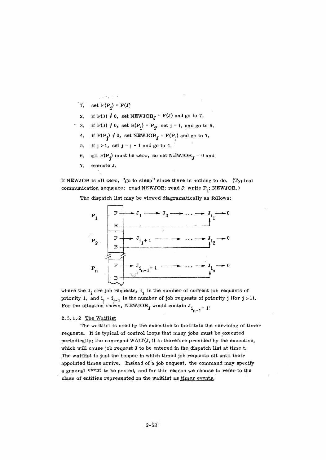
1 set F(P,) = F(J}
2, if F(J) 40, set NEWJOB, = F(J) and goto 7.
3, if F(J) 70, set B(P,) = P,, set j = i, and go to 5.
4, if F(P;) 70, set NEWJOBJ
5. ifj>1, setj=j-1landgoto 4.
= F(P,) and go to 7,
= 0 and6. all F(P,) must be zero, so set NoOWJOB,
7. execute J,
If NEWJOBis all zero, "go to sleep" since there is nothing to do. (Typical
communication sequence: read NEWJOB;read J; write Ps NEW.JOB.,)
The dispatch list may be viewed diagramatically as follows:
P i F ~~ Jy > J5 _——3a0
B }
F—-+—» J. eeJ.Py i,t 1 42
B
aPp ¥ = Jj + 1 ——_—_—" oon J. —_—_ 0
n nel nyo B a) 4
en where the J; are job requests, iy is the numberof current job requests of
priority 1, andi, - i,_, is the numberof job requests of priority j (forj >1).
For the situation shown, NEWJOB, would contain q;n-1
+ 1°
2.5.1.2 The Waitlist
The waitlist is used by the executive to facilitate the servicing of timer
requests, It is typical of control loops that many jobs must be executed
periodically; the command WAIT(J, t) is therefore provided by the executive,
which will cause job request J to be entered in thedispatch list at timet.
‘The waitlist is just the hopper in which timed job requests sit until their
appointed times arrive, Insiead of a job request, the command mayspecify
a general event to be posted, and for this reason we chooseto referto the
" class of entities represented on the waitlist as timer events,
2-58
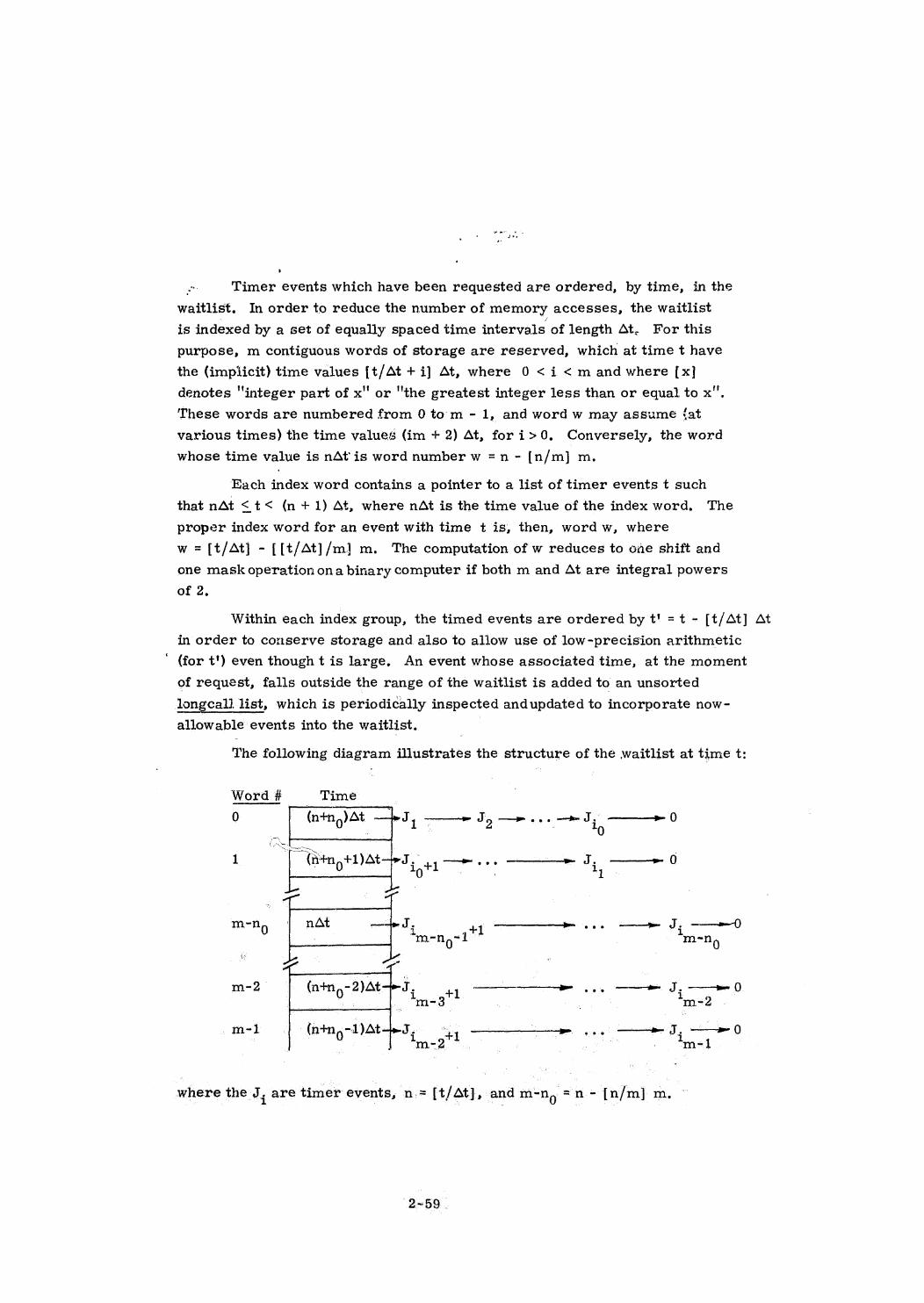
Timer events which have been requested are ordered, by time, in the
waitlist. In order to reduce the number of memory accesses, the waitlist
is indexed by a set of equally spaced time intervals of length At. For this
purpose, m contiguous words of storage are reserved, which at time t have
the (implicit) time values [t/At + i] At, where 0 <i < _m and where [x]
denotes "integer part of x" or "the greatest integer less than or equal to x".
These words are numbered from 0 tom - 1, and word w may assume fat
various times) the time values (im + 2) At, fori>0. Conversely, the word
whose time value is nAt' is word number w =n - [n/m] m.
Each index word contains a pointer to a list of timer events t such
that nAt <t< (n +1) At, where nAt is the time value of the index word. The
properindex word for an event with time t is, then, word w, where
w = [t/At] - [[t/At]/m] m. The computation of w reduces to ove shift and
one mask operation ona binary computer if both m and At are integral powers
of 2,
Within each index group, the timed events are ordered by t' = t - [t/At] Atin order to conserve storage and also to allow use of low-precision arithmetic
(for t') even though t is large. An event whose associated time, at the moment
of request, falls outside the range of the waitlist is added to an unsorted
longcali list, which is periodically inspected andupdated to incorporate now-
allowable events into the waitlist. |
The following diagram illustrates the structure of the waitlist at timet:
Word # | Time
0 (ning)At Jy or Fg eneedy
Ot
1 (nintl)At—rSs44— ., a4 ——_—» 0
a onoT
m-ny Js ; +1 creaming gg —_—— J; -—_—»—{)
m-ny-t m-ny
iZ a \ | | .
m-2 (n+n Bates, oe i Cd,00 i +1 i
{ = _ m-3) - m-=2
_m-1 | (ntny-1)At—»J, 4 OO nee se J. -——»> 0
m-2 m-1
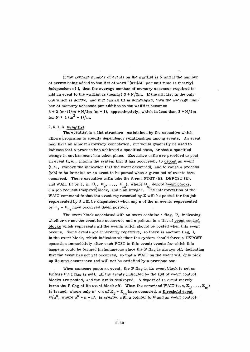
If the average numberof events on the waitlist is N and if the number
of events being added to the list of word '(nti)At" per unit time is (nearly)
independent of i, then the average number of memory accesses required to
add an event to the waitlist is (nearly) 3+N/2m, If the nAt list is the only
one which is sorted, and if it can all fit in scratchpad, then the average num-
ber of memory accesses per addition to the waitlist becomes
3 +2 (m-1)/m + N/2m (m + 1), approximately, which is less than 3 + N/2m
for N > 4 (m2 - 1)/m.
2.5.1.3 Eventlist
' ‘The eventlistis a list structure maintained by the executive which
allows programs to specify dependency relationships among events. An event
may have an almost arbitrary connotation, but would generally be used to
indicate that a process has achieved a specified state, or that a specified
change in environment has taken place. Executive calls are provided to post
an event (i.e., inform the system that it has occurred), to depost an event
(i.e., remove the indication that the event occurred), and to cause a process
(job) to be initiated or an event to be posted when a given set of events have
occurred, These executive calls take the forms POST (E), DEPOST (E),
and WAIT (E or J, n, Ey E,, wees Ea where En denote event blocks, .
J a job request (dispatch)block, andnan integer. The interpretation of the
WAIT commandis that the event represented by E will be posted (or the job
represented by J will be dispatched) when any n of the m events represented
by E, - E, have occurred (been posted).
The event block associated with an event contains a flag, P, indicating
whether ornot the event has occurred, anda pointer to a list of event control
blocks which represents all the events which should be posted when this event
occurs. Some events are inherently repetitive, so there is another flag, I,
in the event block, which indicates whether the system should force a DEPOST
operation immediately after each POST to this event; events for which this
happens could be termed instantaneous since the P flag is always off, indicating
that the event has not yet occurred, so that a WAIT on the event will only pick
up its next occurrence and will not be satisfied by a previous one.
When someone posts an event, the P flag in its event block is set on
(unless the I flag is set), all the events indicated by the list of event control
blocks are posted, and the list is destroyed. A depost of an event merely
turns the P flag of its event block off. When the command WAIT (e,n, Eis ‘issued, where only n' <n ofE
perro E
17 En haveoccurred, a threshold event
E/n", where n' =n -n!', is created with a pointer to Eand an event control
2-60
m)
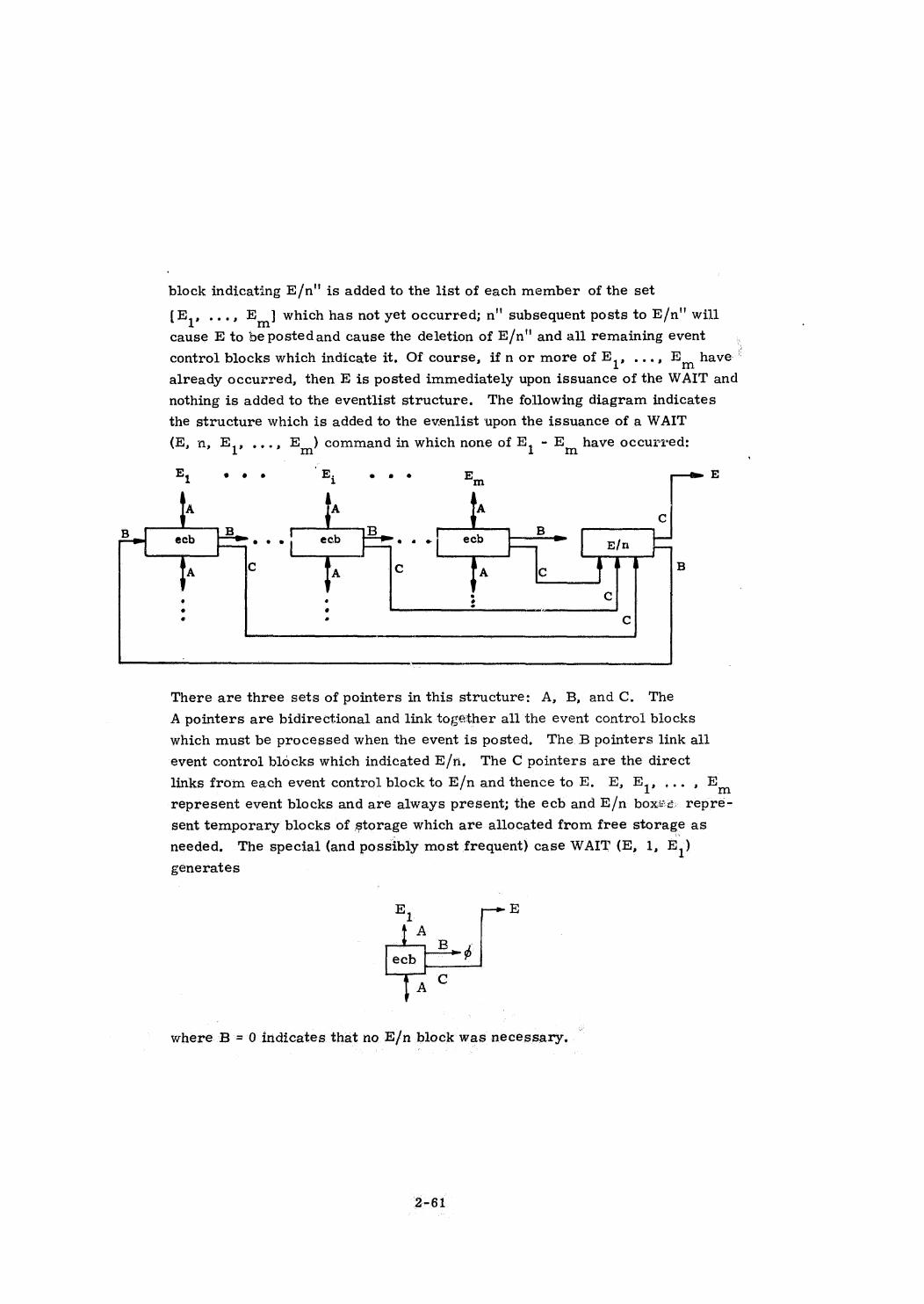
block indicating E/n'' is added to the list of each memberof the set
[E,, ..., HE] which hasnot yet occurred; n" subsequent posts to E/n" will
cause E to be postedand cause the deletion of E/n" and all remaining event
control blocks which indicate it. Of course, ifn or more of E> eeey Eon have.
already occurred, then E is posted immediately upon issuance of the WAIT and
nothing is added to the eventlist structure. The following diagram indicates
the structure which is added to the evenlist upon the issuance of a WAIT
(E, a, E ve E command in which none of EB - En have occured:
1’ oe
E, on Sr) , E; ee @ En ——tee 1
ta A taCc
ecb Bee ee ecb Be ae ecb |B E/n =
[a Cc A jc 14 Cc I B
° e 5 Cc° e = : . }Cy * Cc
There are three sets of pointers in this structure: A, B, andC. The
A pointers are bidirectional and link together all the event control blocks
which must be processed when the event is posted, TheB pointers link all
event control blocks which indicated E/n, The C pointers are the direct
links from each event control block to E/n and thence to E, E, Ey... ED
represent event blocks and are always present; the ecb and E/n box#s: repre-
sent temporary blocks of storage which are allocated from free storage as
needed, The special (and possibly most frequent) case WAIT(E, 1, E,)
generates
Ey men
tA
ecb| é
jae
where B = 0 indicates that no E/n block was necessary. SS
2-61
2.5.2 Process Interlock
The multiprocessor environment is a competitive one; jobs compete
for processor time and processors compete for jobs to do. For some pro-
cesses in this environment, notably those concerned with resource (e.g. pro-
cessor, memory) allocation, it is essential that at most one processorat a
time be engaged in performing the function, A reliable mechanism to prevent
multiple simultaneous allocation must, therefore, be an integral part of such
a system. Common data memory is a likely locus for such a mechanism,
since it is accessible to all processors and since access is synchronized (by the
data bus) so that only one processor at a time has access to a particular
memory.
The interlock scheme proposed here is flexible and simple to imple-
ment, but is completely dependent upon cooperative, 'perfect'' programs:
i.e, it solves only the multiprocessor problem, not the multiprogrammer one,
It is a purely software-implemented scheme, assisted by the hardware only
to the extent that special instructions are provided to make the mechanization
efficient. The basic element of the scheme is a read~and-lock instruction to
memory, which reads out the addressed location and, if the high-order n bits
(n being sufficient to represent any processor number) are zero in a control
word unique to the set of words being accessed, replaces their contents with
the number of the requesting processor, If some lock bit is non-zero(i.e.,
the lock is already locked, the processor "traps" to an executive routine which
may either reissue the command(after relinquishing the bus) or enter a_speci-
fied "user" routine for special action. If the current program is being restarted
(due to processor failure, for example), the executive routine first compares
the number of the (failed) processor with the lock bits, allowing the program
to "pass" the lock, as if it had not been locked, if the numbers match. Since
a basic lock involves a processor number, for restart protection, locked mem-
ory clearly cannot be allowed to exist across job (and therefore processor)
boundaries. A process desiring to set an interjob lock can do so simply by
using one of the remaining bits of the lock word as described below, For
convenience, a routine could supply this service in a standard fashion.
To set an interjob lock, the routine first issues a read-and-lock
instruction. If it passes (i.e., no other processor is testing the interjob,
bit), then the interjob bit is tested; if zero, it is set non-zero, the lock bits
are cleared, the processor restart pointer is updated, andthe leck ''passes";
if, however, the interjob bit is non-zero, only the lock bits are reset and the
locked-lock procedure (e.g., try again later or enter special routine) is.
executed. . : a
2-62
To reset an interjob lock, it is again necessary first to issue a read-
and~lock instruction, Having passed the read-and-lock test, the routine then
resets the lock bits and the interjob bit to zero, and updates the processor
restart pointer.
It is pointed out that the read-and-lock instruction is used during both
set and reset to prevent processor interference, and that successful sets and
resets must be accompanied by simultaneous restart pointer updates (to allow
restarts). It is possible to omit use of the read-and-lock instruction for inter-
job locks if the processor prevents interference by holding the bus (away from
other processors) throughoutthe set and reset procedures; this obviates the
need for a read during reset.
One alternative to the proposed basic scheme is locking by page number,
where the lock is implemented by the memory's associative page table. The
read-and-lock comrnand now locks the whole page containing the referenced
datum, if not already locked, by associating the requesting processor number
with the page number in the page table. All accesses to a locked page cause
"traps" if the lock number differs from the requesting processor number,
The main advantage of this alternative is that only programs which
access data in order to update them need be concerned with locks. Inconsis-
tent (i.e., only partially updated) data access is automatically prevented since
all requests will be trapped if an update procedure is in progress, Its dis-
advantages, however, are (1) cost, due to increased size of the memory page
tables, and (2) loss of flexibility since a page is the minimum lockable unit.
2.5.3 Error Control Function
Design goals of the ACGN multiprocessor computer demand that the
system be resistant to the effects of component failure. In this section, we
define certain classes of failures and describe more explicitly the goals of
error control. We then describe a scheme designed to realize these goals.
We consider as "failures" only those component malfunctions which
are detectable. For any finitely redundant coding scheme, it is possible to
imagine some disaster sufficiently severe so as to preclude correct signaling
of the error to the rest of the system. The case where lightning strikes a
unit and fuses it is an example of undetectable "malfunction". Error detecting
and correcting codes are classified as to the numberof simultaneousfailures
they candetect or correct, Thus, a parity code detects only odd numbers of
failures; a Hamming code corrects (masks) single failures and detects double
2-63
failures, and soon. We define permanent failure as those failures which are
detectable under repeated inquiry; transient failures as those which are not,
One may question the advisability of using a component (say a processor) which
has once failed, even if subsequent testing indicates correct behavior. It is,
of course, possible to consider all failures as fatal and to removetheir
respective components from the system. However, one can imagine cases in
whichall or almost all of a particular component has at one time or another
indicated failures and the choice becomes one of selecting the lesser of several
evils. We shall,: therefore, consider that once-failed componentsmay be deemed
useful; it is these failures which we call transient. Implementation of this
philosophy requires that components which have indicated failures should be
subjected to a validation test, and returned to operational status if the test
result is satisfactory. Additionally, it is necessary to maintain a historical
record of failures for each component, so that one which fails too often may be
removed from the system even if it passes the validation test.
In the succeeding discussion, we shall have occasion to refer to some
components as "infallible", This does not, of course, mean that the component
cannot in fact fail, the lightning bolt case precludes this interpretation. Rather,
we determine some acceptable probability of failure, say e¢ and refer to as
"infallible" any component in the system whose probability of failure is less
than ¢, External systems might be sensitive to such "impossible" failures;however, we consider internal failure of this component to be sufficiently unlikely
that thecost of protection outweighs the probable loss from failure. In addition,
there are some components, the failure of which is sufficient to render recovery
impossible, Since we cando nothing to recover from such failures, we might
as well ignore their possibility.
We may now restate the goals of the ACGN error control system:
1. The system should be resistant to the effects of transient failures;
moreover, these should be transparent to mission programs. By
"transparent" we mean that recovery from such failures will be
handledautomatically by the executive, provided that the mission
program has obeyed the programming conventions required by the
system. -
2. Similarly, permanent failures should be handled transparently
wherever possible. To handle cases of failures in which loss of
data has occurred and in which no automatic recovery is possible,
_ a mission-program-dependentroutine may be specified to. handle
the error. Possible actions of this routine might include recreating
the data, informing the astronaut, or performing a partial or total
fresh start. The.mechanism for specifying such routines might
be similar to that discussed under Section 2.5, 5. |
2-64
3. Fresh start procedures will be implemented in the event of system
lockup, erratic system behavior, and repreated restarts.
The scheme wepropose to realize these goals makes use of hardware
features, executive services and programming conventions. We shall, there-
fore, declare explicitly the assumptions of the ACGN's architecture upon which
our scheme is based:
1, All components of the system are infallible under error detection,
Thismeans that the prebability of the occurrence of an undetected
failure can be made sufficiently small so as to be negligible.
2. Additionally, certain components of the system are infallible under
error correction. Essentially, this means that the probability of
an unmasked error in these components is at least as small as the
probability of the occurrence of an undetected failure in a "fallible"
component, Such (infallible) components include:
a. the bus and its associated control logic
b. prograra memory
c. the I/O Buffer unit, which includes NEWJOB.
3. Pages in erasable memory may fail in a detectable manner; however,
since critical data may be replicated in more than one memory module,
we mayconsider erasable data infallible, even though any particular
erasable module is not.
4, Fallible components may be isolated from therest of the system.
There are, therefore, two sources of errors which must be handled by
the’ executive. |
1. Processor failure
2, Data memory failure.
2.5.3.1 Processor Failure
In general, there willbe two classes of error control programs, one for
processor failure, the other for data memory failure. The major distinction
is that the detection of memory failures will cause an involuntary transfer to
the executive which would thenattempt corrective action. In the case ofa pro-
cessor failure, however, a bit would be set in NEWJOBinformingthe rest of
the system of the offending processor's condition. That processor wouldthen
be "put to sleep", a state in which it-would not respondto generic signalsasking for an interrogation of NEWJOB. | Rather, a special message would
2-65
have to be issued to this processor by number, to "wake it up". This would
have the effect of isolating processors with known failures so that they would
not contaminate the rest of the system by generating bad data, When the
wakeup signal is sent to the failed processor it would presumably execute a
self-check program, the results of which would indicate whether the given
processor was capable of correct performance, If so, the failed job could
be restarted at the point indicated by its restart pointer. If not, it would go
back to sleep until a subsequent successful completion of self-check demon-
strated its usability.
In either case, the jobactive atthe time of the failure must be restarted. In
the interests of completing the job as soonas possible, it wed probably be desir-
able not to await the completion of self-check, but rather to restart the jobon another
processor (presumably the one that discovered the first processor's failure by
investigating NEWJOB). To find the restart pointer, the restart program con-
sults an active job table which is indexed by processor number and which con-
tains the current restart address for every active job. The new processor then
updates its own entry in the active job table to include the current restart
point for the job being restarted, plus the numberof the processor on which the
job was previously run. This will be necessary in the event that, previous to
the restart, the job had locked :ny data in memory. Any attempt to access
that data subsequent to restart would then cause an interrupt, at which point the
executive would consult the ac‘ive job table to see if the current job is in
Restart, and if the number of the previous processor matches the number
recorded in the lock. If so, the access is allowed to take place. If not,
normal locking procedures would have to be followed, It is critical that, if
subsequent to Restart brit prior to the termination of the restarted job the failed
processor successfully completes its self-check, it WAIT on the completion
of the restarted job before exesuting any other jobs, Otherwise the detection
of a lock code equal to the failed processor's number would be ambiguous,
Some conventions concerning the use of the restart pointer should now
be stated.
This pointerindicates the location where the program should be re-
entered should a restart occur, Data contained in scratchpad can not be
assumed valid across phase pointer changes. Therefore, a program may. change
the restart pointer only when the scratchpad is not assumed to,contain the
results ofprevious processing. Thus, an appropriate time to issue such a
phase change might be after a write which completed the update of some ‘datum.
2-66.
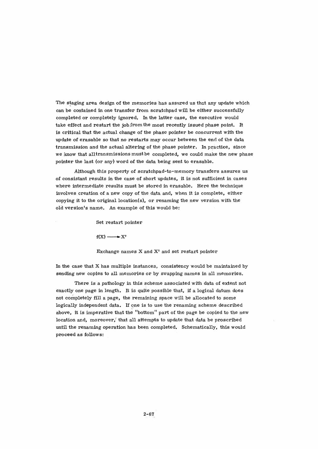
The staging area design of the memories has assured us that any update which
can be contained in one transfer from scratchpad will be either successfully
completed or completely ignored. In the latter case, the executive would
take effect and restart the job.zrom the most recently issued phase point, It
is critical that the actual change of the phase pointer be concurrent with the
update of erasable so that no restarts may occur between the end of the data
transmission and the actual altering of the phase pointer. In practice, since
we know that alitransmissions mustbe completed, we could make the new phase
pointer the last (or any) word of the data being sent to erasable.
Although this property of scratchpad-to-memory transfers assures us
of consistant results in the case of short updates, it is not sufficient in cases
where intermediate results must be stored in erasable. Here the technique
involves creation of a new copy of the data and, when it is complete, either
copying it to the original location(s), or renaming the new version with the
old version's name. An example of this would be:
Set restart pointer
£(X) ——»X'
Exchange names X and X' and set restartpointer
In the case that X has multiple instances, consistency would be maintained by
sending new copies to all memories or by swapping names in all memories.
There is a pathology in this scheme associated with data of extent not
exactly one page in length. It is quite possible that, if a logical datum does
not completely fill a page, the remaining space will be allocated to some
logically independent data. If gne is to use the renaming scheme described
above, it is imperative that the "bottom" part of the page be copied to the newlocation and, moreover, that all attempts to update that data be proscribed
until the renaming operation has been completed, Schematically, this would
proceed as follows: |
2-67
Set restart pointer
o '#(X,) ———Xx,
(a)
'
Exchange names X and X and unlock X and set restart pointer
In the event that the system contains physical locks, either the copy
of xy to Xi or the copy of Xo to X, followed by a rename would be safe, since
the entire page X would be locked by the locking of Xy- The decision of which
way to copy could be made on economic grounds - namely which datum xy or
Xo is shorter, In the event. that logical rather than physicallocks are employed,
the operation would still be safe if we could insure that the bus would not be
relinquished between the points indicated by (a) above.
2.5:3.2 Data Memory Failures
Data memory failures will presumably be detected during attempts to
read or write, These failures will cause exzor messages to be sent to the
requesting processor which will then "trap! ‘0 an executive routine to handle
the failure. Ifthe failure were detected during a read operation, the executive
would consult a weight table which containsthe relative importance of different
data for various phases of the mission. These weights would then be considered
in the light of available system resources (total number of remaining usable
pages) and a decision would be made whether tore-allocate the failed instance
of the page or whether to merely delete it, thereby reducing the number pf --
copies of that page. In any case, the actual failed page would be renamed to”
the ''failed" name and an attempt would be madeto read another copy. When
this procedure is successfully completed, the program is re-entered at the
trap point and allowed to proceed. Subsequent activity could determine the
extent of the failure (whether it was limited to one block or general to the
memory) or else normal attemptsto read from that module would. cause
elimination of failed blocks. Write failure could be handled in the same
‘manner. «. | ~ | :
2-68
Unfortunately, the only way to determine whether a page has failed
is by attempting to read or write it. Ifa particular datum is used infrequently,
it is possible.that all extant copies might indepentently fail before the datum's
use. It might, therefore, be useful to have a program which takes advantage
of periods of low system activity by attempting to read critical data and cor-
recting failures before all copies of a page have failed.
2.5,4 Program-Related Errors
The class of program-~related errors includes those abnormal condi-
tions arising during program execution which do not necessarily imply hard-
ware failure. Events such as arithmetic overflow, zero divisor, memory lock
violation, and invalid address are in this category. Each processor will itself
handle such conditions generated by its program by saving the current instruc-
tion address in a standard scratchpad location and then taking its next instruc-
tion from a memory location determined by the condition which arose,
This behavior has already been referred to in this document as trapping.
For each possible condition, a standard action is supplied by the executive un-
less special action is requested by the current program.
A register of scratchpad (called TRAP) is reserved tocontain the address
of a vector of transfer addresses, each of which serves to specify a processing
routine for a particular condition; to service condition A, a processor takes as
its next instruction address C (C(TRAP) + A) where C(X) denotes the contents
of register X, Each job desiring a nonstandard TRAP pointer must assume
the responsibility for initializing it and protecting it across restarts; if TRAP
is standard, it need not be explicitly initialized or protected by the job, since
both job initiation and restart will initialize TRAP to the standard value,
2.5.5 Hardware Executive Aids
The executive functions performed by each central processor in the
system are done by interrogating or manipulating data in the common data
memory. This convergenceof traffic is a potential system bottleneck, We
must at ieast plan for an alternate approach which eliminates the bottleneck
for computer systems at the very high end of the capabilities scale,
The desired executive hardware, here called Job Stack, would require
_ little processor time to function, and would itself require little timeto execute
"its functions. Such a system is possible and, at least inthe not too’distant
future, may in fact be feasible. The system envisioned is a self-containedassociative processor realized by LSI techniques not readily available today.
The procurement of such a device would raise the computing ability of alarge
multiprocessor system substantially, since it would allevaite two problems
at once,
2-65
The operating speed of the total executive function of one job would
improve by roughly an order of magnitude, Likewise, the availability of the
Executive Hardware would improve to a like degree; hence the delays intro-
duced by processors queuing up for Executive activity would similarly decrease.
These savings are significant in those systerns where 10 or more processors
are still required to handle peak computing load after allowances are made for
system degradation due to the in-flight processor failures,
A job stack is inherently a "hard core" element, that is, its function is
essential to computer operation. It does not lend itself to being replicated in
a gracefully degrading structure, although it is conceivable that it can be im-
lemented this way. If not, it will have to employ error-correcting redundancy :
throughout,
The remainder of this section describes a study of a possible job stack |
structure irrespective of its hardware error control.
2.5.5.1 General Description
The Job Stack described in this section is a special purpose unit which
facilitates job management. Communication between the Job Stack and the rest
of the system is accomplished by transmission of messages over the bus. Job
_, request messages are issued either by processors or the 1/O Buffer. Included
“ta a job request is the priority of the job and the time at which it should be
run. The Job Stack receives these messages, maintains them in a time-threaded
list, and transmits an indication when any job or group of jobs has come due to
be run, Actual dispatching of jobs is performed according to an algorithm by
an executive program run on any processor (2.5.1.1). The Job Stack also
receives job acceptance messages and failure messages from processors, and
maintains a list indicating the current activity of each processor. :
2.5.5.2 Advantage of Separate Job Stack
An advantage of the separate Job Stack is that processors can issue job
requests, indicate job acceptance, or indicate processor failure by simply
; placing a message on the bus. Incorporation. of the information in these
messages into the appropriate list within the Job Stack is performed by the. ;
Job Stack itself, without’further involvement of the issuing processor. In order
for these functions to be performed by a purely software executive system using
the simple, passive Main Data Memory, it would be necessary for processors
to spend time running program and possibly to wait for Main Data Memory |
accessibility. Also, the Main Data Memory and the bus would not be available
2-70
to other processors during the time required to manipulate the executive lists.
Providing the Main Data Memory with list manipulating capabilities would reduce
the bus traffic, but would not make the Main Data Memoryitself available tu
other users while the executive lists are being manipulated.
2.5.5.3 Job Stack Organization ~
The Job Stack consists of an Outstanding Request List, an Accept List,
a Staging Area associated with the Accept List, a Free Storage List, anda
Stack Status Register and Bell.
2.5.5.3.1 Outstanding Request List
This list contains already-issued requests for jobs that have not yet
been run. Each entry contains the information that was present in the message
that issued the request. Included in each entry is the priority of the job and the
time at which it should be run. The list is threaded,i.e. ranked, by this time value.
When a group of jobs becomes due, a message is sent on the bus (bell
is rung) indicating that jobs are ready to be executed, Any ordering on priority
or other criterion is performed by the executive program run on any processor.
t~ reads a portion of the Outstanding Request List, orders it as appropriate, and
sends it backto the Job Stack, Now job requests may be taken off the top of the
list one at a time by individual processors which then run the appropriate job.
2.5.5.3.2 Accept List and Staging Area
2.5,5.3,2.1 Normal Uses
This isa simple, unthreaded list containing one entry per processor
and indicating what job each processor is currently running and in what phase.
Each entry contains the information that was present in the corresponding
Accept Message. An Accept Message is issued by a processor whenit first
takes on a job, and each time it is necessary to change the phase of a running
job. Notice that, since the Accept List is not threaded, the entry corresponding
to a given processor can be found directly without list thread chasing.
If a jobrunning on a processor issues a request for a new job, the
request is placed into a register taken from free storage and linked to the
‘issuing processor's entry in the Accept List. A staging aréa may be built up
in this manner as needed,. At the next phase change for a given job, all job
requests that may have accumulated in the staging area associated with the
appropriate processor's entry in the Accept List during the current phase are
threaded into the Outstanding Request List by time due. Requests for new jobsare not threaded directly intothe Outstanding Request List to prevent possible
duplication of the request for the new job in the event that the issuing job should
fail and be restarted; a oo |
2-71
2.5,5.3,2.2 Executive Uses
The executive program also makes use of the staging area associated
with the Accept List. It reads the group of entries that are due now from the
top of the Outstanding Request List, re-orders them(probably based on priority),
and replaces them into the Outstanding Request List via the staging area
associated with the processor running the executive program. A newlist of
request messages is threaded in the staging area in the order sent by the
processor, The processor then sends an Incorporate-List-and-Accept Message
which replaces a specified numberof entries at the top of the Outstanding
Request List with the re-orderedlist of requests built up in the staging area
of the processor running the executive program. The replaced portion of the
Outstanding Request List is returned to free storage.
The processor running the executive program may keep one job request
of the list it read, not send it back to the stack, and run the job itself. The job
it keeps is obviously the one it determines should be run first, The Accept
part of the Incorporate-List-and-Accept Message would accept the new job.
Once the group of entries in the Outstanding Request List that are due
now is ordered, a free processor will take the top job and run it. It reads the
top request from the list, and sends nothing back into its staging area. The
processor then sends anIncorporate-List-and-Accept Message which eliminates
the top job request from the Outstanding Request List and accepts the new job.
2.5.5,3.2.3 Processor Failure Messages
When a processor fails, a Failure Message indicating which processor
has failed is sent to the Job Stack. This failure indication is placed into the
entry in the Accept List correspondingto the failed processor, The previous
information about what job was running is not destroyed, Thus the Accept List
maintains a record of which processors have failed, which jobs they were
running prior to processor failure, and whatphases these jobs were in, This
information permits restartingthesejobs. _
2.5.5.3.3 Free Storage
Free Storage is a threaded list linking all available registers in the Job
Stack. It serves both the Outstanding Request List and the staging area
associated with the Accept List. Registers are obtained from this list when
. needed, and returned to it when available.
2-72 =

2.5.5.3.4 Bells
When the Job Stack determines from the Stack Status Register that the
executive program should be run, it sends the DO EXECUTIVE Message on
the bus. This is known as the bell. The StackStatus Bits are read by the
processor running the executive program to determine what function needs
to be performed. These status bits indicate the following conditions:
1. The Outstanding Request List has an unordered group of requests
for jobs needing to be run,
2. The Outstanding Request List has an ordered group of requests
for jobs needing to be run.
3. The Accept List has a processor Failure Message that needs
attention.
The Stack Status Bits are modified both by the stack itself and by program
action.
Whena group of requests in the Outstanding Request List becomes due,
the Stack Status Bits are set to indicate that an unordered group of requests
need to be run, and the DO EXECUTIVE message is sent on the bus. TheDO EXECUTIVEis sent repeatedlyuntil the executive program, responds by
reading the Stack Status Bits and locking the Bell and Stack.
After the executive program has re-ordered the top group of the Out-
standing Request List and returnedit to the Job Stack, the executive program
changes the Stack Status Register to indicate that an ordered group of requests
is ready to be run, and unlocks the Bell and Stack. The DO EXECUTIVE message
is sent repeatedly until the executive program responds by reading the Stack Status
Bits and by locking the Bell and Stack. After the executive program has taken the
top job from the Outstanding Request List and accepted it, it unlocks the Bell and
Stack. The executive program is called repeatedly in this way until the ordered
group at the top of the Outstanding Request List is exhausted,
Once the top group of the Outstanding Request List has been ordered,
if it becomes necessary to insert a new request into this group, the Job Stack
changes the Stack Status Bits to unordered, This occurs when either a new-
request is issued that belongs in the top group or when the next group of
requests in the Outstanding Request List becomes due before the ordered top
group is exhausted,
When the Job Stack receives qa Failure Message, the Stack Status Bits
areset to indicate that a processor failure needs attention, and the DO
EXECUTIVE message is sent on the bus. The DO EXECUTIVEissent repeated-
ly until the executive program responds by reading the Stack Status Bits and
lockingthe Bell and Stack. a oe
2-73
2.5.5.3.5 Bell and Stack Lock
Locking the Bell and Stack affects the beil (DO EXECUTIVE message),
the Stack Status Register, and the Outstanding Request List. The Bell and
Stack is locked with a record of the processor ‘hat locked it. If this processor
fails, the Bell and Stack is unlocked. Locking the Bell and Stack does not lock
the Accept List, which is always available.
When the Bell and Stack is locked, the Job Stack is inhibited from
sending any DO EXECUTIVE messages on the bus. This prevents the Job Stack
from issuing subsequent DO EXECUTIVE messages once the executive program
has responded to a DO EXECUTIVE message. There should be only one occur-
rence of the executive program at a time.
Locking the Bell and Stack causes the Stack Status Register to be avail-
able only to the processor in whose name the lock was performed. During
this situation, any attempted changes to the Stack Status Bits by a processor
other than the locking one or by the Job Stack itself are accumulated in a buffer
(not the staging area associated with the Accept List) and are 'OR'd with the
current Stack Status Bits when the Bell and Stack is unlocked.
When the Bell and Stack is locked, the Outstanding Request List is un-
available to any processor other than the locking one. Any attempt to thread
a new request into the Outstanding Request List during this period will cause
the request to be placed ina buffer, (This is not the same as the staging area
associated with the Accept List.) When the Bell and Stack is unlocked, any
requests in the buffer will. be threaded into the Outstanding Request List by
time.
2.5.5.3.6 Processor Failures
Whena processorfails, a Failure Message indicating which processor
has failed is sent on the bus. The Job Stack changes the Accept Message for
that processor into a Failure Message without destroying the information in
the Accept Message, eliminates any Job Requests found in that processor's
staging area, and sets the Failure Bit in the Stack Status Register. if the Bell
and Stack was locked in the name of the failed processor, it is unlocked, Any
buffered Job Requests are threaded into the Outstanding Request List by time;
any buffered information for the Stack Status Register is 'OR'd with the current
Stack Status Bits.
The Job Stack now sends the DO EXECUTIVE message on the bus. Afree processor responds by running the executive program, reads the Stack
Status Bits, locks the Bell and Stack, anddetermines from the Stack Status
Bits that it should run the failure portion of the executive program.
2-74
2.5.5.3.6.1 Failures of Normal Programs
The failure program reads the Accept List and takes note of all Failure
Messages. Any Failure Message found with phase 77 has already been attended
to by a previous execution of the failure program. For all other failure
messages, the corresponding failed programswill be restarted, A Job Request
is issued for each failed job at the phase found in the Failure Message. Then
the phase in the Failure Message is changed to 77, to indicate that this failed
job has been restarted. Note that the Failure Message is not destroyed and
leaves a record of which processor has failed. After attending to all Failure
Messages, the failure program removes the Failure Bit from the Stack Status
. Register and unlocks the Bell and Stack.
In restarting failed jobs, care must be exercised to prevent duplicating
or losing the request for the failed job in case the failure program itself
should fail. The failure program issues a request for the failed job as though
it had been requested by the failed processor. Note that the request enters
the staging area of the failed processor, not that of the processor running the
failure program. This strategy is used so that a single Accept Message causes
the phase of the Failure Message to be changed to 77 and the request for the
failed job to be incorporated intothe Outstanding Request List. Before issuing
the request for the failed job, it is necessary for the failure program to unlink
(that.is, return to free storage) the staging area of the failed processor, there-
by deleting any unincorporated request for the failed job that may been issued
by a previous partial execution of the failure program.
2.5.5,3.6.2 Failures of the Executive Program (Ordered or Unordered)
Failures of the executive program (ordered or unordered) are probably
handled differently from failures of normal jobs. Since the Job Stack may be
in a different state from that which was ineffect. when the executive program
began to run, it seems desirable not to restart the executive program at the
phase at which it failed. Any contamination caused by partial executionsof
the executive program is removed if necessary, and the execution program is
allowed to run from the beginning corresponding to the latest state of the Job
Stack, If theexecutive program is self-cleansing, removal of this contamina-
tion by the failure program is not necessary. After the failure program has
finished, the bell will ring again, indicating the lateststate of the Job Stack.
Note that partial executions of the executive program do not alter the Stack
Status Bits. If the Job Stack Status does not change, the bell ringing again
will cause the same portion of the executive program as had failed to be
executed from the beginning. | :
2-75
2.5.5.3.6.3 Failures of the Failure Program
Failures of the failure program are probably handled differently from
failures of normal jobs. Of course, a failure of the failure program itself sets
the Failure Bit just as any other failure does, and causes the failure program
to be run, An unambiguous record is maintained in the Accept List of which
Failure Messages have not yet successfully been attended to. Any complete
execution of the failure program canattend to all outstanding failures, There-
fore, itis unnecessary to restart failed occurrences of the failure program.
Any contamination caused by partial executions of the failure program must be
removed if necessary. After having attended to all outstanding Failure Messages,
the failure program removes the Failure Bit from the Stack Status Register.
2.5.5.4 Applicability to Other Approaches
The Job Stack system for job management described above is by no
means the only approach. For example, a pure software implementationusing
passive memory as previously discussed, or an implementation using memories
with list manipulating properties,are other approaches, The problems uncovered
in this study should be similar to those encountered by other mechanizations.
Many of the concepts proposed should apply in general to the other approaches,
even though specific details might differ.
a
2.5.5.5 Messages
The messages described in this section are used for communication
between processors and the Job Stack. They are included to illustrate the
principles described above and are noc necessarily the most compact set.
In general a processor issuing a message may not be able to, or may
choose not to, send information in every field within the message. Some
particular code in a field will be interpreted by the Job Stack as an order to
continue to use information it already has for that field. Some other code in a
field will be used to indicate that the Job Stack should blank that field.
1. JOB REQUEST (Y, T, Jas Pi Je q)
This is a request for phase ¢ of Job J; to be run at time T, with
priority Y, requested by job Jy. from processor P..
P, is needed for later incorporation or deletion of this job request,
dependingon whether P; reaches a phase change point or fails.
J, may be useful for tracing job history.
2-76
Accept phase ¢ of Job Jj. running on processor Pia’ with priority
Y. (This job was originally requested by job Jy)
Changing phase performsa validation/incorporation function on job
request messages and data transfers issued by processor Pin since its
last phase changé. To incorporate the job requests, it threads thern
into the Outstanding Request List. To validate data transferred to the
Main Erasable Memory, it declares the data good and discardsthe old
information.
End-of-Job is a special case of changing phase. Phase 77 could be
used,
3, FAILURE (P_)m
Processor Pi has failed. Change the appropriate Accept Message
to a Failure Message in the Accept List, keeping all the information
that was present in the Accept Message. Job request messages and data
transfers issued by processor Pin since its last phase change (and
therefore not yet validated/incorporated) aré flushed,
Receipt of a Failure Message sets the Failure Bit in the Stack
Status Register and rings the bell,
A Failure Message with phase 77 in the Accept List indicates that
the specified failure’ has been attendedto.
4, DO EXECUTIVE JOB
This is the bell by which the Job Stack indicates that the executive
program should be run.
5, ACCEPT, LOCK BELL AND STACK, READ STACK STATUSOW; Ji Pm’? Jy ¢)
This is similar to the simple Accept Message, but it also locks the
Bell andStack and.reads the Stack Status Register. The Job Stack sends.
back the Stack Status Bits together with the name of the processor having
locked the Bell and Stack,
6. ACCEPT AND WRITE STACK STATUS (¥, J,, Ps dys $sSTACK STATUS)
Thisis similar: to the simple Accept Message, but it also writes ©
new Stack Status information into the Stack Status Register. Ifthe Job.
Stackis locked by another processor, message #8.is sent. back by the
Job Stack. (Used by failure program to,’remove the FailureBit from
the StackStatus Register.) _ —
2-77
7. READ OUTSTANDING REQUESTLIST (G, P
G is the number of groups to be read beginning at the top of the Out-
standing Request List. A group is a collection of job requests to be done
at the same time. Pin is the processor issuing this message. If the
Job Stack is unlocked or locked by Pi the requested information is sent
and the Job Stack is locked in the name of Pint If the Job Stack is
already locked by another processor, the requested information is not
sent and message #8 is sent.
Note G = 0 is a special case for reading the top job request message
only.
8. JOB STACK IS LOCKED (Pi P,)
This message is sent by the Job Stack in response to an attempted
access of the Job Stack by processor Po if the Job Stack is already
locked by some other processor Pie
8, ACCEPT, INCORPORATE INTO OUTSTANDING REQUEST LIST,
UNLOCK BELL AND STACK(Y, Js Pin Jie ¢, N)
N is the numberof entries in the Outstanding Request List that are
being replaced by a new list. This new list has been sent to the Job
Stack by a series of job request messages preceding this message.
Pn is the processorthat sent the new list. The entries making up the
new list are in processor Pin's staging area in the Job Stack,
This message unlocks the Bell and Stack. It also declares that
the group of requests thai‘are due now in the Outstanding Request List
is ordered,
If Pu decides to run one of the jobs whose request it read, the.
accept information included in this message is pertinent to that job.
If not, the accept information in this message causes a simple phase
change for J,, the job that read and is storing the list.
N equals 1 is used when the top job only is read from the ‘Outstanding
Request List. No job request messages are sent to the Job Stack.
This message removes the top job from the Outstanding Request List
and accepts the top job.
If the Job Stack is locked by another processor, message #8 is sent
back by the Job Stack.,
2-78
10, ACCEPT, UNLOCK BELL AND STACK(Y, Jj. Pw Jie ¢)
This is similar to the simple Accept Message, but is also unlocks
the Bell and Stack. It does not alter the Stack Status Register, If the
Job Stack is locked by another processor, Message #8 is sent back by
the Job Stack. (Used by the failure program to conclude).
11. READ ACCEPT LIST (P|)
The Job Stack sends the Accept List to processorP|. (Used by
failure program.)
12. CHANGE PHASE OF EXISTING MESSAGE (PL, Pos ¢)
The processor issuing this message (P,) changes the phase of some
other processor (P,) to ¢. Any job request messages issued by, or in
the name of, Ps since its last phase change are incorporated into the
Outstanding Request List. This message does not change the phase of
P,. It does not change the message name of the message whose phase
it changes in the Accept List. (Used by the failure program to mark a
Failure Message as attendedto.)
13. UNLINK (P_, P,)
The processor issuing this message (P,) unlinks the staging area
associated with the Accept List entry of another processor (P,). (Used
bythe failure program to prevent possible duplication of a request for
a failed job.) : |
14, ECHO (P,)
The Job Stack acknowleges receipt of the message sent by processor
P,. to the Job Stack. This message is used in cases where there would
be no other response,
2.6 Input-Output Buffer
2.6.1 Messages
Communication between the multiprocessor and its environmentis via
a serial time-multiplexed bus commonto many systems. To avert a chaotic
situation in which several systems are simultaneously trying to transmit,
there must be either a channel for scheduling, or else a master-slave hierarchy
among the systems. The latter is what is proposed here, with the master role
played by the input-output unit, called I/O Buffer, of the multiprocessor.
2~79
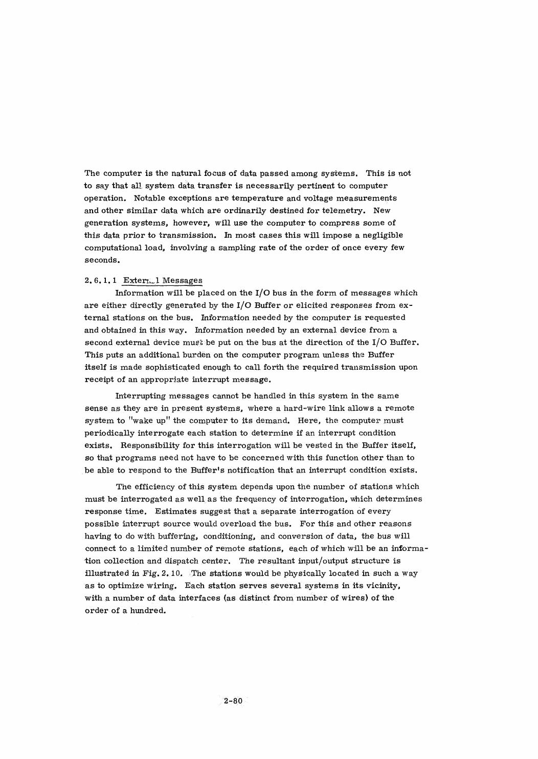
The computer is the natural focus of data passed among systems. This is not
to say that all system data transfer is necessarily pertinent to computer
operation. Notable exceptions are temperature and voltage measurements
and other similar data which are ordinarily destined for telemetry. New
generation systems, however, will use the computer to compress some of
this data prior to transmission. In most cases this will impose a negligible
computational load, involving a sampling rate of the order of once every few
seconds,
2.6.1.1 Exterr..1 Messages
Information will be placed on the I/O bus in the form of messages which
are either directly generated by the I/O Buffer or elicited responses from ex-
ternal stations on the bus, Information needed by the computer is requested
and obtained in this way. Information needed by an external device from a
second external device musibe put on the bus at the direction of the I/O Buffer.
This puts an additional burden on the computer program unless the Buffer
itself is made sophisticated enough to call forth the required transmission upon
receipt of an appropriate interrupt message.
Interrupting messages cannot be handled in this system in the same
sense as they are in present systems, where a hard-wire link allows a remote
system to "wake up" the computer to its demand. Here, the computer must
periodically interrogate each station to determine if an interrupt condition
exists. Responsibility for this interrogation will be vested in the Buffer itself,
so that programs need not have to be concerned with this function other than to
be able to respond to the Buffer's notification that an interrupt condition exists.
The efficiency of this system depends upon the number of stations which
must be interrogated as well as the frequency of interrogation, which determines
response time, Estimates suggest that a separate interrogation of every
possible interrupt source would overload the bus. For this and other reasons
having to do with buffering, conditioning, and conversion of data, the bus will
connect to a limited number of remote stations, each of which will be an informa-
tion collection and dispatch center. The resultant input/output structure is
illustrated in Fig. 2.10. :The stations would be physically located in such a way
as to optimize wiring. Each station serves several systemsin its vicinity,
with a number of data interfaces (as distinct from number of wires) of the
order of a hundred.
2-80
LInternal Busto Processorsand Memories
1/O BUFFER
External Bus
SYSTEM A
SYSTEM BSTATION 1 bE i
SYSTEM C
SYSTEM Dq||
| SYSTEM W
STATION N i
SYSTEM Z
Fig. 2.10 Input-OutpuiStructure
Though it is premature to define message formats, some general re-
marks can be made about them, Input and output messages vary considerably
in length and frequency of occurrence, and advantage should be taken of this
wherever feasible. Interrupt interrogations occur particularly frequently,
and should be as brief as possible. The minimum length of such a message
would be the numberof bits required to specify a station (probably five) plus
a special operation code for the interrupt interrogation function (possibly as
few as two). Thus the byte concept might well be extended to the external
bus. Error detection bits would, of course, be added to the byte in trans-
mission. For operation codes other than interrupt interrogate, a second byte
would be sent which would specify a particular data interface to be activated.
Succeeding bytes would contain data, if any, being sent out of the computer.
Responses would be sent at the conclusion of the computer's transmission by
the station involved, the format being essentially the same. For example,’
an interrupt response would be asingle byte identifying the station and giving
a yes-no indication. If yes, succeeding bytes identify the interrupt. If no,
the response is ended, Terminal bytes might be identified by a bit in each
byte reserved for the purpose,
2.6.1.2 Internal Messages
The messages which commute between the I/O Buffer and the external
stations are related to information which is transferred on the computer's
internal data bus. Input and output data, for example, have destinations and
origins, respectively, in the processors, Interrupt responses reaching the
1/O Buffer are translated into executive commands and sent onto the computer.\\
Reformatting and resynchronizing are inevitable tasksin the transfer
of data between the external I/O bus and the internal computer data bus. This
is one of the principal functions of the I/O Buffer, and is a sufficiently
sophisticated operation to demand a versatile organization, The Buffer will |
bear some resemblance to a processor, having a sequence generator, a local.
buffer (scratchpad) memory, and an arithmetic unit, or sorts, to edit and
manipulate the data.
Information directed to the Buffer on either bus is recognized and
stored, and processed according to a microprogram elicited by control bits
in the message, When transmission is called for, the Buffer puts thetrans-
lated messages into a queue to wait for access to the appropriate bus.
Sufficient storage must be provided to queue as much information as may
accumulate between bus accesses,
2-82
2.7
2.6.2 Error Control
The I/O Buffer, I/O bus, and the remote stations will have to be either
fully masked or else replicated for substitution ‘in order to achieve high
reliability, Although a gracefully degrading organization is conceptually
possible, it would be awkwardin this particular application.
Modular redundancy is an attractive means of error control, particular-
ly since the I/O system is highly serial, which minimizes the numberof voting
circuits required, ,
For remote stations, triple redundancy with voted outputs are recom-
mended, Depending on actual reliability assessments, switchable spares may
have to be furnished at each station. If they are not, then either manual re-
placement will be made, or else reversion to simplex mode effected when a
failure occurs.
For the bus, error detection by coded redundancy, such as parity or
Hamming codes, will be sufficient to supplement a triply redundant voting
structure. In this way, error detection is still provided in the event ofa
multiple bus error or failure, and voter reconfiguration is easily made so as
to use one good bus out of three,
For the 1/O Buffer, a selection of various error control methodsis to
be used, Two or three extra Buffer units will be on-line or ina standby mode
for redundant or simplex operation with substitution for failed units, Masking
and error detection schemes may be appliedinternally to each Buffer unit as
described for the Processor, but whether or not and how much are questions
to be answered later.
To summarize, error control for the input/output system of the pro- .
-cessor is going to be costly comparedto the cost of the bare input/output sys-
tem above. It should be remembered, though, that this will still be a minor
fraction of the total multiprocessor cost.
Programming Aids
2.7.1 General
There are certain programming hardships intrinsic to a system in which
parallel control paths occur as a matter of course. These were present to a
degree in the AGC because of the relative timing independence of some control
loops and will certainly.become somewhat more serious in the ACGN due tothe
addition of a multiprocessorétrusture. In particular, the proper use of locks
(2.5,2), restart pointers (2,Be3), and erasablememory sharing requires more.
2-83
attention to detail than was previously necessary. Much of this burden has
been assumedby the executive, by extending its function from that of a pure
job-dispatcher to that of a resident monitor, but it remains for the program-
mer to ensure consistent use of the executive and to allocate use of scratch-
pad and common erasable accesses properly.
To aid the programmerin this task, to simplify the conversion from
experimental to working models, to reduce the probability of undetected coding
and communication error, and to facilitate a high degree of program modular-
ity and interchangeability, extensive use of a "high-level" algebraic compiler
language is strongly recommended. For those situations ir: which the compiler
language is not readily applicable, and there will certainly be some, an
assembler whose macrofacilities and other features allow assembly programs
to mesh easily with compiler-language programs and with the executive should
be provided. Finally, a program is required that collects and integrates com-
piler and assembler output, accomplishing the final phases of storage allocation,
implementing a symbolic "patch" capability, and producing final output in
simulatable or executable form.
The primary function of the collector is to allow partial revision of.
the computer's program load without complete re-compilation/assembly.. It
has been demonstrated on commercial systems that the time savings due to
this technique can be considerable. Certain symbolic information is preserved
by the compiler and assembler, and passed along with the compiled/assembled
output to the collector. In this way, symbolic references between separately
compiled/assembled pieces of coding can be resolved as actual memory locations
are assigned to programsand blocksof data storage.
As far as the’ development plan for support software is concerned, the
following observations are offered. Since the executive must exist before
checkout of higher-level programs can proceed very far, the assembler should
be completed early, and the collector and simulator soon thereafer, Simulator
.input requirements must be defined before the collector can be completed; and
similarly, collector input requirements will affect compiler/assembler design.
Since the final phases of the compiler and thase of the assembler are very
- similar in function and must produce identically formatted output, it may be
desirable to mergethe design processes of the compiler and the assembler
in such a way that the final phases may be commonto both, thus reducing cost
and improving reliability. | | |
2-84—
2.7.2 The Compiler
It has long been the goal of computer users to place the burden of man-
machine communications on the machine. To this end there has been a trend
toward the use of application-oriented higher-level ("compiler") languages
which are automatically translated into absolute machine code, The traditional
reasons for writing in a higher-level language is that, ideally, source code is
mcre concise and easy to write than it would be if expressed in machine or
symbolic assembly language. Thus, the application expert may communicate
with the machine in a form familiar to him ~ he does not have to worry unduly
about details of machine construction.
Unfortunately, compiler-produced code is traditionally wasteful of
storage and execution time, and attempts to make it better have resulted in
the exploitation of vagaries of the compiler's implementation. While such
attempts cannot be categorically denounced as bad practice (they have often
made compiler language coding possible where more straightforward coding
would have resulted in object programs which would not fit into the machine),
they nonetheless detract from the accessibility of the resulting program.
Furthermore, the sophisticated compiler-language programmer must be
aware not only of his problem and the language of the computer, but also of
details of the compiler's operation. As an example consider the Fortran
, expression for a polynomial
= ayey= ax +bxte
which would be expressed as
Y=Ct+xX * (B+A * X)
to avoid redundant multiplications, Obviously, a compiler capable of
optimizing its own code to the extent that it is nearly as good as that produced
by human coders is desired, While it is not clear that this goal is realizable,
compilers capable of highly efficient code have already been produced and it
is our feeling that any loss of efficiency will be more than overcomeby gains
in uniformity, quality, and accessibility of the resulting source coding.
Additionally, programming conventions (use of locks, etc.) which would
normally be enforceable only by the prog.ammer's discretion can be built
into the compiler and, if all code is compiler-produced, the resulting programs
will contain the desired characteritistics asinfallibly as though they had been
2-85

built into the machine. In a system as highly dependent upon synchronization
as a multiprocessor, this,feature is a strong argument for the use of compiler-
level languages.
Optimizing compilers are frequently very slow at compilation time.
For this reason we recommendeither a rapid "pre-compiler" to eliminate
keypunch and elementary syntax errors inexpensively or, alternatively, a
compiler with an optional optimization phase which would be invoked after
programs have been partially debugged. In cases where it is absolutely
necessary, critical programs could be coded in assembly language but, for
those reasons stated above, this is to be avoided if pogrible. .
Additional features of a compiler for the ACGN would include:
1. A language capable of expressing easily and concisely problems
in dynamics and control.
2. Output (object code) compatible with that produced by the ACGN
assembler. This would be directly readable by the collector
described in Section 2.7.1.
3. A symbolic pseudo-assembly language listing of the resulting
object code would be producedto facilitate program debugging -
particularly the reading of dumps.
4. The computer would produce instructions to the collector concern-
ing communication between programs, erasable allocations, re-
quests for generation of unique names, etc,
“2-86
3. LOGICAL/ ELECTRICAL DESIGN
3.1 Processor Design
3.1.1 Component Trends
The strongest influence in the logical/ electrical design of the computer
subsystem has been the promise of large scale integrated circuitry (LSI) to
come in future years. Not only will it render logic a more expendable design
commodity than wires and other connections, but it will force its users to
conform to its inconveniently small ratio of pins to active elements. This
can lead to some radical departures in design, One contemplates the idea of
an entire processor on a single piece of semiconductor material with all inter-
connections internally made, and asks how such devices could be used in
quantityto obtain high performance. Such a device, if it could be made, would
have a suitably low pin to gate ratio, but it remains to be seen whether and
how it could be employed in the desired way.
In the more immediate future, LSI will appear as scatchpad storages,
full adders, shift registers, and various specialized items such as D/A and
A/D converters and multiplexers. At the present time many of these devices
are obtainable in abbreviated sizes using evolving microcircuit technology
said to be at the stage of ''medium scale integration", or MSI. Where early
microcircuits had a few gates per package, present MSI has many, and can
yield a substantial increase in component density over computersof the AGC's
generation. High density is advantageous in the speed/ power trade-off due to
reduced stray reactances.
More important, it has now becomefeasible to use flip-flop memories
whose access time is lower than the magnetic memories used before. This is
of particular value in microprogramexecution, where the storage of auxiliary
and temporary quantities has been at a premium limiting the scope of instructions.
This speed can also be traded off against complexity, in that a byte-organized
memory and arithmetic unit uses less equipment and fewer connections and is
easier to check than a long-word processor. The expense is in terms of
number of memory cycles and microprogram complexity. Cycle speed and
high- density microprogram storage minimizes this expense.
3, 1. 2. Scatchpads
The organization of a scatchpad data memory, feasible inpresent
technology and appropriate for the processor in question, is next discussed.
The basis for the design is a proposed monolithic 8 X 8 storage cell array
with address decoding, a circuit whose feasibility has been demonstrated in
research, althoughnot yet in production. Each bit is individually addressable,
so the device is equivalent to a 64-werd X one-bit fragment of memory. Ten
devices would be needed to make a 64-byte segment with ten-bit bytes. Sixteen
such segments, or 160 devices would makeup the full scratchpad complement
of 1024 bytes. As discussed earlier, this is the numberof bytes that can be
indexed or addressed by a single byte of ten bits, and is therefore a convenient
size to work with for the present.
A concept of the array structure is shown in Trig. 3.1. Using the
notation of Fig. 3.2, Fig. 3.3 illustrates the scratchpad organization. Itis a
16 X 10 rectangular grid of array devices, with address lines common to members
of a row and data lines common to members of a column. Thetotal address is
ten bits long. The low order six bits are common to all of the arrays and
decoded therein. The high order four bits are decoded externally into sixteen
read and write enable lines to serve the sixteen rows. Data exchange is with
a buffer register inthis construct, whereas in practice it may be with multiple
buffers in a serial organization, or directly with central and arithmetic
registers in a parallel organization.
_ Multiple address registers are incorporated in this memory in order
to resolve the problems which arise from the byte organization of the processor.
Storage of result bytes wili normally alternate with fetching of operand bytes,
which generates a good deal of address changing and address indexing. Information
transfer activity is greatly reduced by furnishing separate base addresses for
operands and result, ‘and providing indexing capability for each. The memory
responds to whichever address register is enabled by its gate signal. Each
index register is capable of incrementing its contents by #1, and may be
arranged so as to initiate an increment at the trailing edge of the gate signal.
Physically, the scratchpad would fit on a ten-inch-square boardif
conventional dual in-line packages were used, and would be smaller using
flat packs. Thickness would be a small fraction of an inch using a multilayer
board.
Although circuit speed is certainly a consideration, the performance
requiredof this memory is not extreme. An access time of about 200 nanoseconds
is probably adequate. This is easily met with bipolar transistors,and there
are good prospects for field- effect devices and hybrids to do a satisfactory
job.
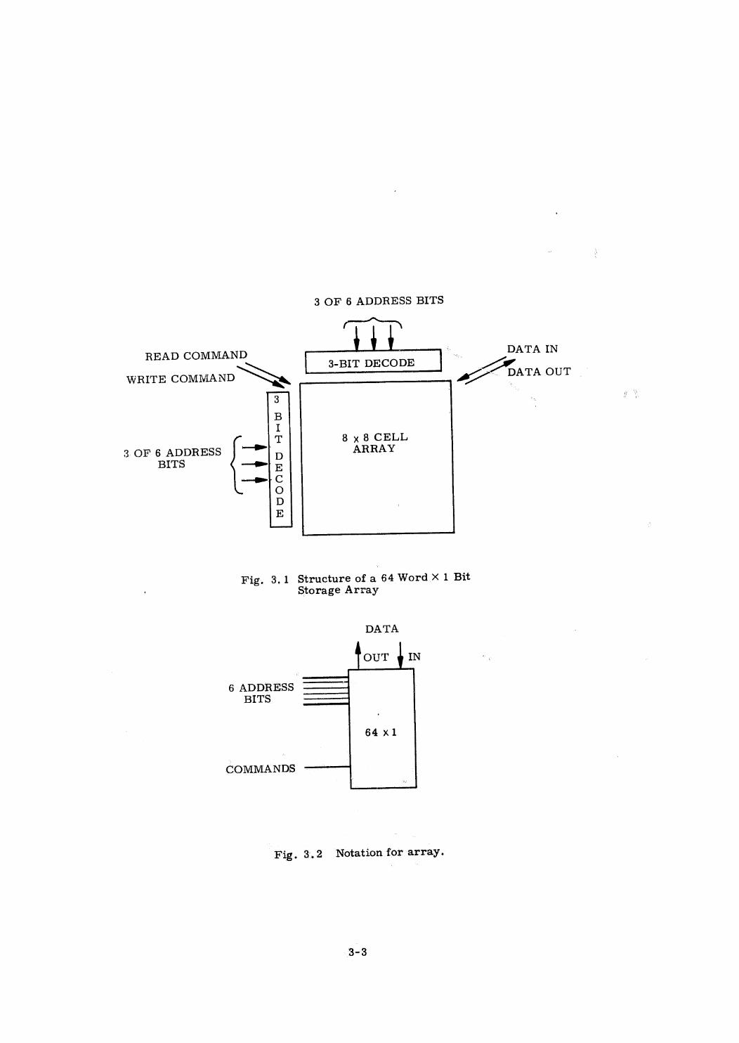
3 OF 6 ADDRESS BITS
titREAD COMMAND oO pata IN
3-BIT DECODEWRITE COMMANDyu. aDTA OUT |
3 | :
BIT 8 x 8 CELL
3 OF 6 ADDRESS
|
"| ARRAYBITS —Pi rb
—e} COD
E
Fig. 3.1 Structure of a 64 Word X 1 Bit
Storage Array
DATA OUT @IN
6 ADDRESSBITS
COMMANDS
Fig. 3.2 Notation for array.
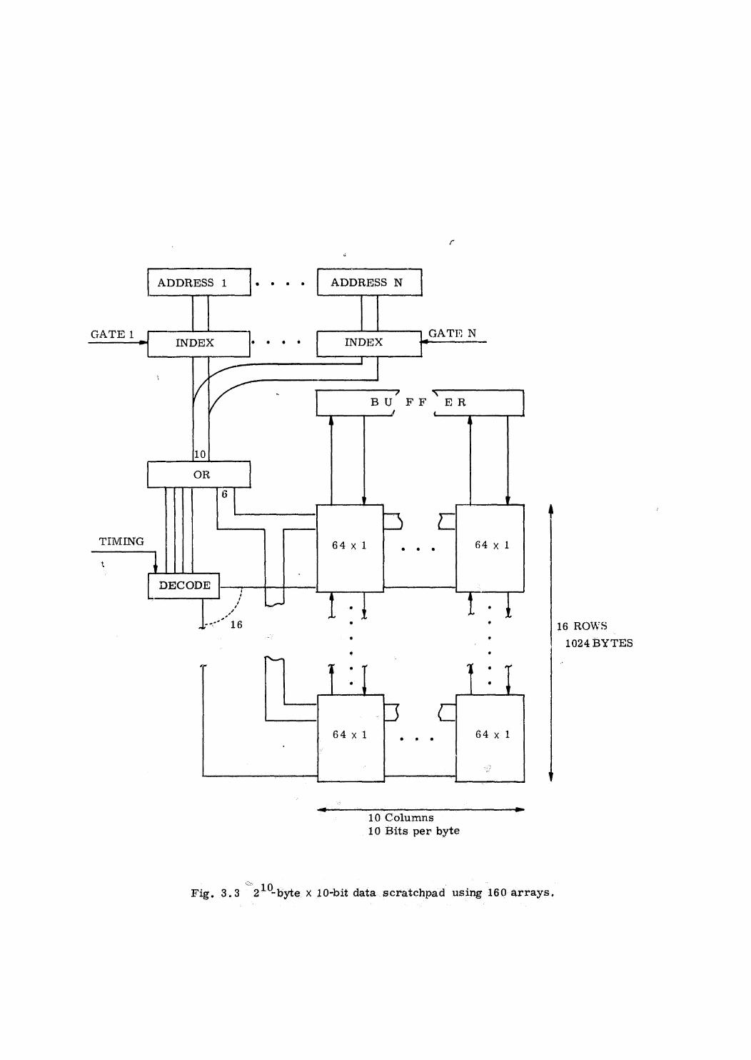
ADDRESS i o 6 2 ADDRESS N
GATE 1 GATN> INDEX oe 8 INDEX jo.
]
\— _BU FF ERJ
10
OR
6
TIMING 64x1 ae 64x 1
x
DECODE :
LA 7 dn De16 ’ ’ 16 ROWS |
: * ° 1024 BYTES
64x 1 Se 64x 1
- Y
~<—<_- a
10 Columns
10 Bits per byte
Fig. 3.3 21°-bytex 10-bit data scratchpadusing 160 arrays.
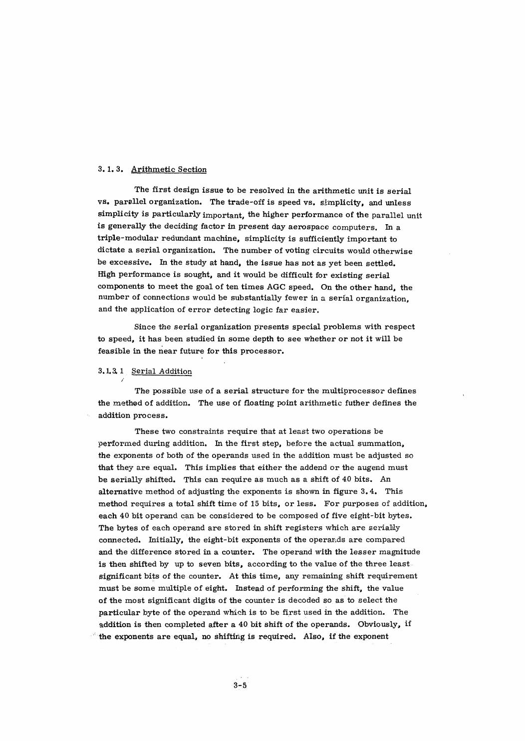
3.1.3. Arithmetic Section
The first design issue to be resolved in the arithmetic unit is serial
vs. parallel organization. The trade-off is speed vs. simplicity, and unless
simplicity is particularly important, the higher performanceof the parallel unit
is generally the deciding factor in present day aerospace computers. Ina
triple-modular redundant machine, simplicity is sufficiently important to
dictate a serial organization. The numberof voting circuits would otherwise
be excessive. In the study at hand, the issue has not as yet been settled.
High performance is sought, and it would be difficult for existing serial
components to meet the goal of ten times AGC speed. On the other hand, thenumberof connections would be substantially fewer in a serial organization,
and the application of error detecting logic far easier.
Since the serial organization presents special problems with respect
to speed, it has been studied in some depth to see whetheror not it will be
feasible in the near future for this processor.
3.1.21 Serial Addition?
The possible use of a serial structure for the multiprocessor defines
the method of addition. The use of floating point arithmetic futher defines the
addition process.
These two constraints require that at least two operations be
verformed during addition. In the first step, before the actual summation,
the exponents of both of the operands used in the addition must be adjusted so
that they are equal. This implies that either the addend or the augend must
be serially shifted. This can require as much as a shift of 40 bits. An
alternative method of adjusting the exponents is shown in figure 3.4. This
method requires a total shift time of 15 bits, or less. For purposes of addition,
each 40 bit operand can be considered to be composed of five eight-bit bytes.
The bytes of each operand are stored in shift registers which are serially
connected. Initially, the eight-bit exponents of the operar.ds are compared
and the difference stored in a counter. The operand with the lesser magnitude
is then shifted by up to seven bits, according to the value of the three least
significant bits of the counter. At this time, any remaining shift requirement
must be some multiple of eight. Instead of performing the shift, the value
of the most significant digits of the counter is decoded so asto select the
particular byte of the operand whichis to be first used in the addition. The
addition is then completed after a 40 bit shift of the operands. Obviously, if
“the exponents are equal, no shiftirig is required. Also, if the exponent
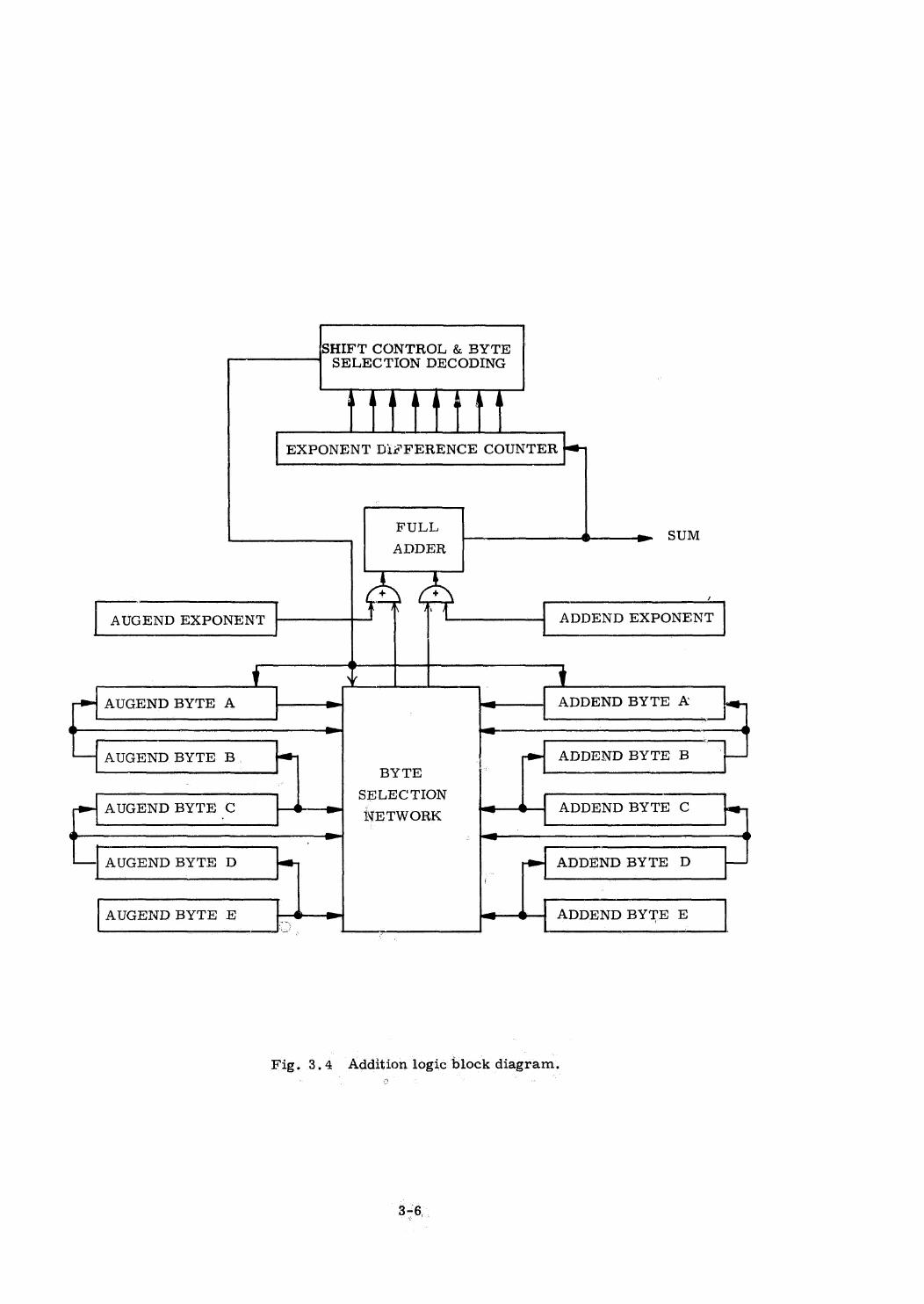
SHIFT CONTROL & BYTESELECTION DECODING
LnEXPONENT DisFERENCE COUNTER
— SUM
+ + /
AUGEND EXPONENT Qo ADDEND EXPONENT
i t 4 AUGEND BYTE A |} . jwg——--—| ADDEND BYTE A
AUGEND BYTE B. ADDEND BYTE B BYTE
SELECTIONAUGEND BYTE Cc NETWORK ADDEND BYTE C
t
| AUGEND BYTE D ADDEND BYTE D
AUGEND BYTE E ADDENDBYTE E
Fig. 3.4 Addition logic block diagram.
3-6,
difference is greater than 40 the sum is simply the greater of the two operands.
In the above discussion of addition no mention was made of a choice for the
representation of a negative number. Three choices are sign and magnitude
notation, one's~complement, and two's-complement. Use of sign and magnitude
notation has the advantage that data is in a form that can be used directly in
multiplication and division, An additional advantage is that data dumped frorn
computer memory can be more easily comprehended, This is useful during
program verification. A disadvantage of sign and magnitude notation is that
operands cannot be directly added when their signs disagree. This prohlem
can effectively be overcome by comparing the signs of the operands before
adding them. In the event of the signs disagreeing, the complement of the negative
operand is applied to the full adder. This is feasible bezause the operands, —
are stored in shift registers where the complement of a bit may be selected.
At the beginning of the addition the complementof the first bit of the negative
operand is presented to the full adder along with an initial carry input. This
is equivalent to serially introducing the two's complementof the negative
operand to the adder. The summation is thus performed using two's-complement
arithmetic. A remaining problem is that the result of the addition, when
negative, will be in two's complement form. This must be then converted to
sign and magnitude representation. In the proposed serial machine this would
require an additional 40 bit shift time. Another possibility is to form both the
sum and its complement. One of these results would have the magnitude in
correct form. This technique requires that each sum bestor'ed in an individual
register as itis formed. Since it is desirable that the final result appears in a
particular register, an additional 40 bit shift may be required. In any case
sign and magnitude notation will require one additional 40 bit shift duringthe
addition. This additional time requirement is not compatible with the performance
goals of the processor. For this reason some other choice must by madefor
negative numbernotation. .
Another possikibility for negativenumber representation is the one's
complement form. This notation has the advantage that a positive number
may be negated by taking its logical complement. This is an advantage only
if the negation can be performed in a parallel operation. This will probably
not be possible in a serial machine. A major disadvantage is that an end
“around carry into the least significant order is required if a carry is propagated
through the sign bit during addition. With a serial logic structure this would
require an additional 40 bit shift time. Thus the one's~complement
representation is eliminated from consideration for the same reason as for
Oo | a1
the sign and magnitude notation.
The remaining choice is the two's complement notation. With this
representation the adder inputs are in a directly usable form, Also, the sum
is in correct form. The only disadvantage is that a 4Qbit shift time is
definitely required for the negation of a positive number. For these reasons
the two's complementnotation is the most likely candidate for negative number
representation.
3.1.3.2. Subtractioti
The subtraction process has the samme constraints as addition. A
possible implementation would be to provide a full subtractor to form the
difference. A more economical approach would be to complement the
subtrahend and perform an addition with the minuend. This could be done
with no cost in time if the two's complement of the subtrahend is formed as
it is introduced to the adder circuit. As mentioned previously this can be
accomplished by selecting the logical complement of the subtrahend and
applying a carry input to the adderat the first bit time.
3.1.3.3 Serial Multiplier
A straightforward multiplication algorithm would be to ‘conditionally
add the shifted multiplicand into a partial product sum accordingto whether
or not the corresponding order of the multiplier is a one. Since both the
multiplicand and the multiplier are 40 bits long, full serial operation would
require a 40 shift addition repeated 40 times for a total of 1600 shift times.
This method, while inexpensive in hardware, is prohibitively long.
Instead, an algorithm was chosen which forms 2. partial product sum
while using eight bit bytes of the multiplier. The method of multiplication _
can be understood by considering the tabular multiplication, process, where
offset rows of partial products are added together to obtain the product. In
the case under consideration, binary arithmetic with 40 bit words are used.
This would result in 40 rows of one's and zero's. The methodchosenis to
serially add eight rows of partial products together during one 48 bit shift of
the multiplicand. It is seen that this is equivalent to forming the sum ofthe partial
products using one eight-bit byte of the multiplier. This is accomplished by |
shifting the multiplicand serially, least significant digit first, through an eight
bit shift register. Each bit of the multiplicand in the register is combined with
a correspondingbit in the first byte of the multiplier using the logical AND©
function. The eight resulting AND outputs are then added together simultan-
3-8
eously. This forms the sum of one columnof the eight partial products of the ,
first byte of the multiplier. The process continues until the entire 48 bit
partial product sum is serially formed and then stored. The least significant
eight bits are part of the final product. The other 40 bits must be added into
the appropriate columnsof the partial product sum. This is accomplished by
enteringthe 40-bit partial product sum serially into the eight-bit sums formed
using succeeding multiplier bytes. In order to perform this sum a nine-input
simulataneous binary adder is needer. After processing each byte of the multi-
plier eight new bits of the final product are formed, and 40 bits, representing
the partial product sum, are stored temporarily. At the end of five 48-bit
shifts of the multiplicand the complete 80-bit product is formed. A block
diagram of the multiplication circuitry is shown in figure 3.5. The multiplier
and the multiplicand are each initially stored in shift registers. Floating
point arithmetic is assumed with each factor normalized so that the most sig-
nificant digit is a one. Also both factors are assumed to be in true, uncom-
plemented form. For simplicity, the logic blocks required for normalization,
product sign determination, and product exponent formation are not shown.
A total of 17 eight-bit shift registers are required. The design ofa
typical stage of a shift register is ‘discussed in a later section. The 40-_
bit multiplicand, stored in five registers, is restored as it is used during the
multiplication.process. The 40 bit multiplier is initially stored in five eight-
bit registers. After the use of each byte of the multiplier, that byte is :
destroyed by an eight-bit shift. The register space freed by this shift is
used to store the final eight-bit product bytes as they are formed. Six addi-
tional eight-bit registers are used to hold the intermediate partial product
sums. One additional eight-bit register is used to hold part of the multipli-
cand during the formation of the nine-bit product sum with the adder.
At the beginning of a multiplication cycle:the first byte of the multiplier
is present at the bit product gates. A 48-bit shift is performed on the multi-
plicand in order to form the partial prodiict sum corresronding to the first
multiplier byte. The eight-bit products are entered into the adder and the
resulting sum is entered serially into the partial product register. The
partial product sumformationis done underthe contirol logic during the 48-bit
shift phase A. During the eight-bit shift phase Bthefirst multiplier byte isdestroyed, and the second multiplier byte’is presented to the bit product gate.
At the same timethe least significant eight bits of the final. productalre |
entered in the vacated multiplier register. Aftershift phaseB the forty-bit
partialproduct sum is availableto bepresentedserially to the adderduring the.° : ee . : A .
3-9
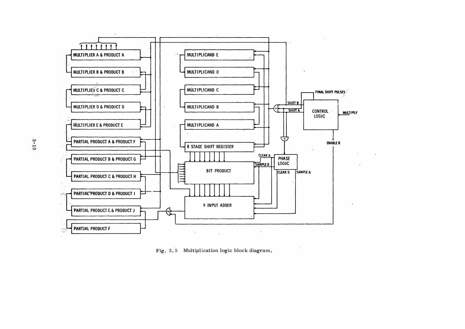
OTe
oe
TrttttthtMULTIPLIER A & PRODUCT-A
MULTIPLICAND E
MULTIPLICAND D
MULTIPLICAND C {|
4 MULTIPLICAND B
MULTIPLICAND A
PARTIAL PRODUCT B & PRODUCT G
8 STAGE SHIFT REGISTER
MULTIPLIER B& PRODUCTB > bY
- nUPLIEKCe PRODUCT C
4 MULTIPLIER D & PRODUCT D
MULTIPLIER E & PRODUCT E
PARTIAL PRODUCT A & PRODUCT FF
_
PARTIAL PRODUCT ¢ & PRODUCT H
ammipl
ee, —<~e
PARTIALPRODUCT D & PRODUCT|
PARTIAL PRODUCT £.& PRODUCTJ
—s—e7
BIT PRODUCT
—
9 INPUT ADDER
PARTIAL PRODUCT F Fig. 3.5 Multiplication logic block diagram.
FINAL SHIFT PULSES“
SHIFT B J* SHIFT A CONTROL © MULTIPLY
LOGIC -
ENABLE B
CLEAR APHASE
SAMPLE D LOGIC
CLEARD {SAMPLE A
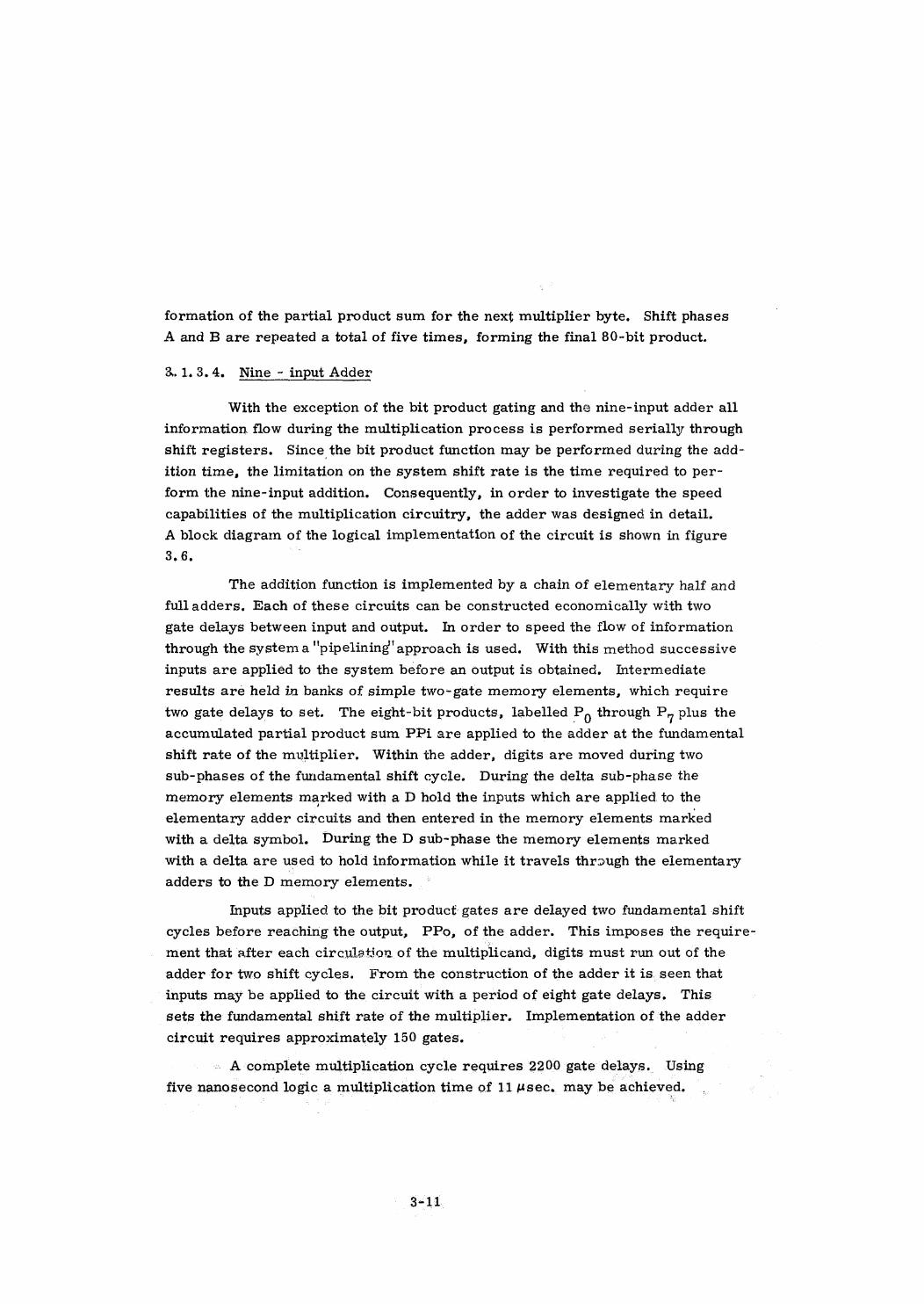
formation of the partial product sum for the next multiplier byte. Shift phases
A and B are repeated a total of five times, forming the final 80-bit product.
& 1.3.4. Nine - input Adder
With the exception of the bit product gating and the nine-input adderall
informationflow during the multiplication process is performed serially through
shift registers. Sincethe bit product function may be performed during the add-
ition time, the limitation on the system shift rate is the time required to per-
form the nine-input addition. Consequently, in order to investigate the speed
capabilities of the multiplication circuitry, the adder was designed in detail.
A block diagram of the logical implementation of the circuit is shown in figure
3.6,
The addition function is implemented by a chain of elementary half and
fulladders, Each of these circuits can be constructed economically with two
gate delays between input and output. In order to speed the flow of information
through the systema "pipelining "approach is used. With this method successive
inputs are applied to the system before an output is obtained. Intermediate
results are held in banks of simple two-gate memory elements, which require
two gate delays to set. The eight-bit products, labelled Po through Py plus the
accumulated partial product sum PPi are applied to the adder at the fundamental
shift rate of the multiplier. Within the adder, digits are moved during two
sub-phases of the fundamental shift cycle. During the delta sub-phase the
memory elements marked with a D hold the inputs which are appliedto the
elementary adder circuits and then entered in the memory elements marked
with a delta symbol. During the D sub-phase the memory elements marked
with a delta are used to hold information while it travels through the elementary
adders to the D memory elements.
Inputs applied to the bit productgates are delayed two fundamental shift
cycles before reaching the output, PPo, of the adder. This imposes the require-
ment that after each circulationof the multiplicand, digits must run out of the
adder fortwo shift cycles. From the construction of the adder it is, seen that
inputs may be applied to the circuitwith a period of eight gate delays. This
sets the fundamental shift rate of the multiplier. Implementation of the adder
circuit requires approximately 150 gates. .
» A complete multiplication cycle requires 2200 gate delays. Using
five nanosecond logic a multiplication time of 11 usec. may be achieved.
(3-11
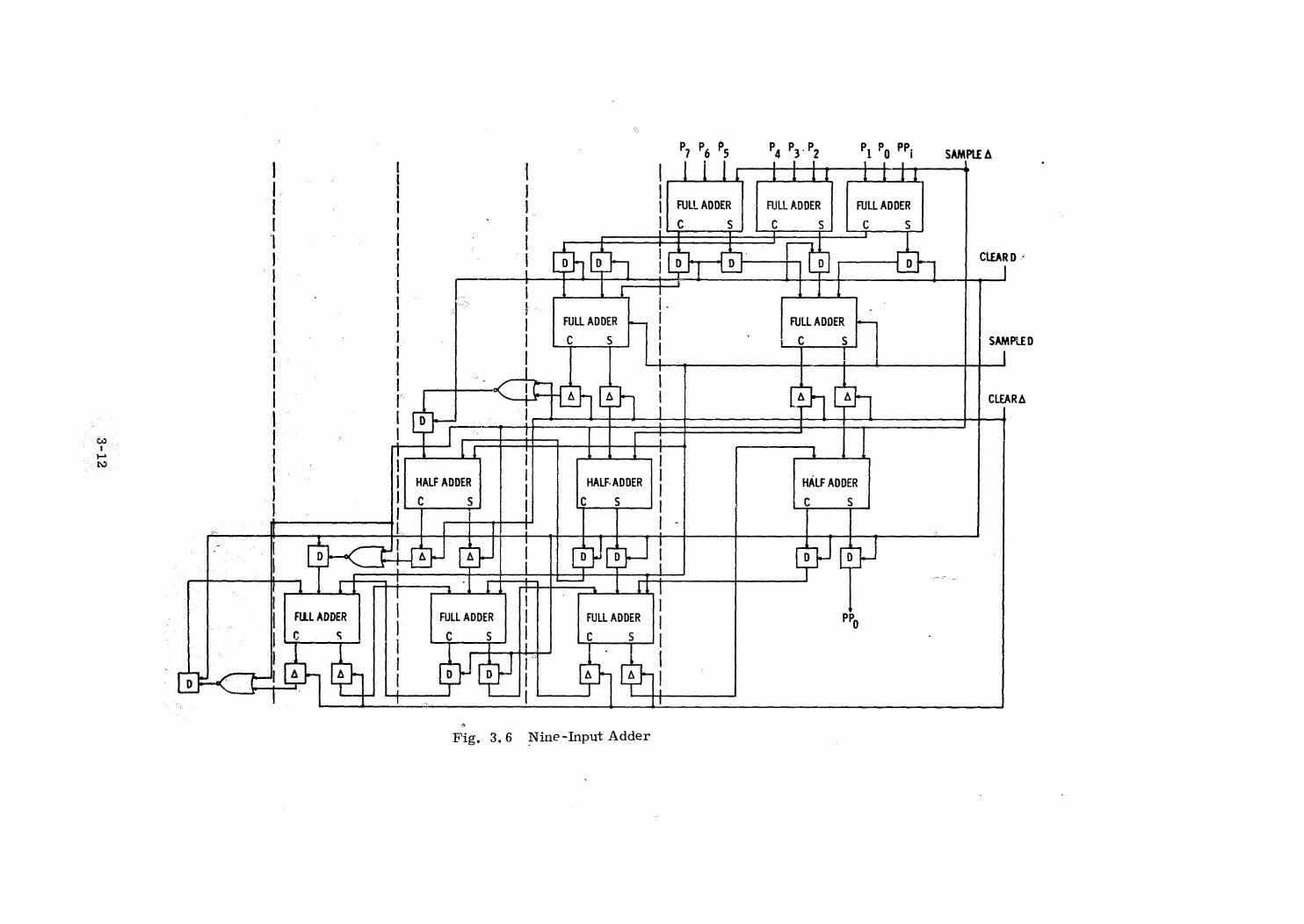
ere
|
FULL ADDER
Cc
HALF ADDER
C $s
HALF- ADDER
S
FULL ADDER FULL ADDER
C 5
Fig. 3.6 Nine-Input Adder
FULL ADDER FULL ADDER
s
HALF ADDER
FULL ADDER
CLEAR-
SAMPLED
CLEARA
3.1.3.5. Bidirectional Shift Register
In the operation of the serial multiplier previously described it is implied
that information in the shift registers must be able to move in both directions.
This is necessary because during the formation of the partial product sum the
multiplicand was operated on serially using the least significant digits first.
This requires a shift to the right. However, normalization of both the multi-
plicand and the multiplier is most conveniently done by shifting to the left.
Thus the need arises for a bidirectional shift register.
A possible design of a typical stage of such a shift register is shown in
figure 3.7, Its implementation uses a single logical element, the NOR gate,
which could be used in a preliminary construction using discrete components.
As compared with the cost of implementing the corresponding single~direction
shift register, one additional gate and two gate inputs are required. Also, the
bidirectional shift register will operate at the same speed as the corresponding
single direction shift register. In addition to the inputs required to shift
information into the shift register stage, inputs are shown which may be used
to externally loadthe stage by the application of a logical one in the absence of
a shift pulse.
During normal operation, in the absenceof a shift pulse, information
is held in gates B and C, and FandG. A right or left shift enable applied to
gates Dor E respectively selects theoutput of the stage to either the left or
right of the stage in question. The arrival of a shift pulse clears gates Band
Cc. “During this time gates F andG hold the input to the next stage. On the
decay of the shift pulse the input is stored in gates B and C, and then F and.G.
The operation of the shift register stage is hazard free if uniform gate
delays are assumed. If gates B and C have exceptionally long delays, the input
to the stage may not be stored before it disappears. This should not be the case
if the shift register is formed from gates on the same solid gate chip. The
shift register operates with a theoretical minimum period of five gate delays.
Two delays are required to apply the input, and three gate delays are required
to store the input after the decay of the shift pulse. .
3.1.3.6. Division
As was the case with multiplication, a hardware implementation of
division using a simple serial approach would be excessively time consuming.
For binary arithmetic using 40-bit operands a total.of 40 serial additions and/or
subtractions must be made, | consuming 1600 shift times. A variable division
3-13
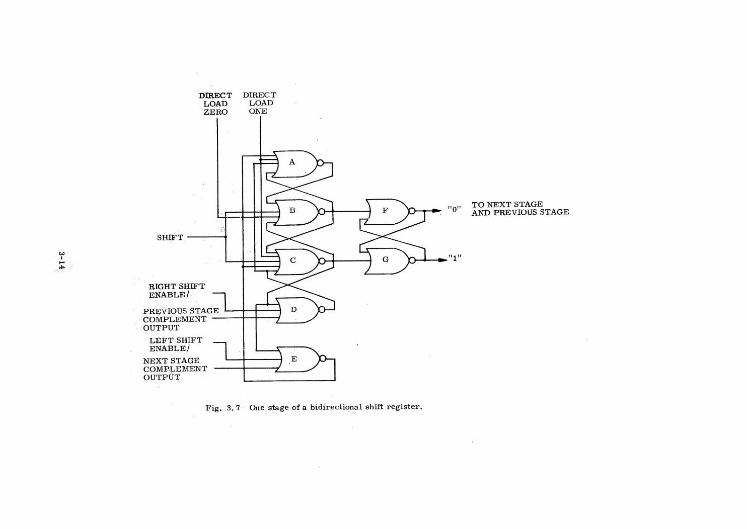
PI-€
- OUTPUT
DIRECT DIRECTLOAD LOADZERO ONE
\ B i ng TO NEXT STAGE4 : AND PREVIOUS STAGE
SHIFT
Cc | G my"
RIGHT SHIFTENABLE/.
- PREVIOUS STAGE | D-COMPLEMENT |
LEFT SHIFT —ENABLE/
NEXT STAGECOMPLEMENTOUTPUT :
Fig. 3.7: One stage of a bidirectional shift register.
time algorithm exists* which would reduce the divide time by a factor of about
2.5 on the average. This still does not reduce the longest possible division
time.
Unfortunately, the serial multiplication algorithm discussed ina
previous section has no known inverse which could be applied to division.
Consequently, in order to decrease division time some parallel information
handling may have to be introduced. One possibility is to use a parallel byte
structure, where the eight bits in a single byte are transmitted in parallel and
successive bytes in a word are processed serially. With such a machine
organization a divide time about twice as long as the multiplication time could
be achieved.
Without considering the gating needed for parallel byte handling, the
amount of logic required is comparable to that needed for multiplication.
3.1.3.7. Logic Functions
In addition to the arithmetic operations described above, the
multiprocessor will be able to perform the logical OR, AND, and EXCLUSIVE
OR functions for two variables. In addition the NOT function, or the logical
complementation of one variable will be available. These functions are
implemented by shifting the desired operand(s) serially into a Switching net-
work providing the desiréd functions. During the shifting time the appropriate
logical function in the network is selected, and its output is stored serially in
a shift register. Each logical operation would require one 40-bit shift time.
3.1.4 Sequence Generator
The heart of the sequence generator is a read-only memory for micro-
programs and certain program routines which would be implemented by a braid
memory containing on the order of 10° bits. The sizing of the braid would be |
such as to deliver 256 or 512 bits per memory cycle. Taking the smallest num-
ber, and a conservative estimate of a one-microsecond cycle time, we arrive
ata minimum microprogram execution rate of 256 megabits per second per
processor. Nowif the arithmetic unit and scratch pad speed is suchas to allow
five byte transfers per microsecond,it follows thatat least 51 bits are available
per average byte transfer as control pulse generators. |
¥High-Speed Arithmetic in Binary Computers, O. L. MacSorley, IRE
Proceedings, January 1961. ° oo :
3-15
In all likelihood, the total numberof control pulses will be about fifty,
so that an organization appears possible wherein a simple correspondenceis
made between memory bits and control pulses. Parity or other redundant bits
provide memory error detection. Indeed, by testing the amplified control
pulses instead of the raw memory outputs, the error detection coverage is ex-
tended that far,
Parity checking for fifty bits at a time is quite expensive, requiring
52 exclusive-OR operations in six levels. It would be more economical to check
in smaller groups of bits at the expense of storage capacity. Such structure
would also increase the likelihood of multiple error detection,
A second attractive format is to encode the control pulses. Assume
that no more than five control pulses are simultaneously generated, which is
a perfectly reasonable assumption. Further assumethat there are fewer than
64 control pulses, Thus 6 bits uniquely specify a control pulse and 5 X 6 = 30 bits
are sufficient to specify all five. Thirty bits do the work of 50 this way, and
further economies are realized if some code positions are restricted to subsets
of the control pulse set, Parity can be employed within each code, and a one-of-
n checking circuit can verify the output of each decoder.
A simple arithmetic operation (add, subtract) on two five-byte quantities
would require about ten byte transfer times, or about 500 bits of microprograms
in the absence of any effort to economize on such bits. Using this as a representa-
tive operation among the various transfers, fetches, and complicated operations,
and assuming the order of one hundred instructions, we estimate about 50, 000 bits
of microprogram. It is conjectured that a like number of bits will be devoted to
local programs.
3.1.5 Multiplexer
The multiplexers which interface with the data and instruction buses
can:be considered in two pieces, the output synchronizer, which is the multi-
plexer proper, and the buffer, which couples the busand the priyessor, particu-
larly with respect to input information.r
3.1.5.1 Output Synchronizer
This circuit receivesan enable Signal from another circuit like it in
another unit. Some time later this circuit transmits an enable signal to a like
circuit in still another unit. If there is a-transmission to be made, ‘the outgoing «
enable is withheld until the transmission is concluded, Otherwise the enable is
passed on with a. minimum ofdelay, i.e. sufficient to prevent positive feedback
latching around the enabling ring. These are particularly vulnerable parts of
3-16-
3. 2
the multiprocessor, since an unmaskedfailure in one of these circuits defeats
an entire bus. One possibility is to have multiple independent buses for band-
width and/or reliability enhancement, The use of such a scheme seemsquite
likely, though its impact on processor design is not discussed in this report.
The enable logic is not particularly complex. It does have to handle
asynchronous inputs, which meansthat it is rs,t utterly trivial; nevertheless
it is readily amenable to triplication and voting, The circuit is responsible for
generating the outgoing enable, for initiating the transmit sequence in the pro-
cessor, and for blocking outputs to the bus unless the enable is properly present.
Its inputs are the incoming enable, a signal expressing the processor's desire
to transmit, and a signal indicating processor failure.
3.1.5.2 Buffer
The basic elements of the decoder are shown in Fig. 3.8. Information
on the bus is shifted into a staticizing register denoted INREG, and immediately
transferred to INBUF so that the next word can follow directly into INREG. Since
the destination of information depends on the nature of the transmission, i.e.,
message vs address vs data, etc., the contents of INBUF are examined to de-
rive commands to the sequence generator when appropriate. The decoder
serves this function.
Information to be transmitted is sent to OUTBUF to wait for OUTREG
to be available. After transfer to the latter register, the information is shifted
onto the bus under control of the sequence generator and the output synchronizer.
The information appears simultaneously at the receiver, and is compared to
verify the transmitter and receiver circuits, Thebuffer will employ integrated
parallel - serial registers capable of 20 to 30 megabits per second speeds,
Memory Design
3.2, 1 Memory Elements
Common memory units will have memories containing the order of 10°
” bits each plus paging and other logic to enable autononous and asynchronous
operation, Three candidates for rnemory cells are to be considered: semi-
conductors, magnetic films, and. magnetic cores.
The stateof the semiconductor art and its immediate prospects are such
that the. order of 10° bits is about as much as may beexpected to be available in
a single device, The order of 10 devices would be required in each unit, there-
fore, which is within reason, Equally reasonable is the power consumption of
thesedevices. The lowest power figures which have been reported from experi-
mentai work have about 10 microwatts per bit using MOS technology and standby
3417.
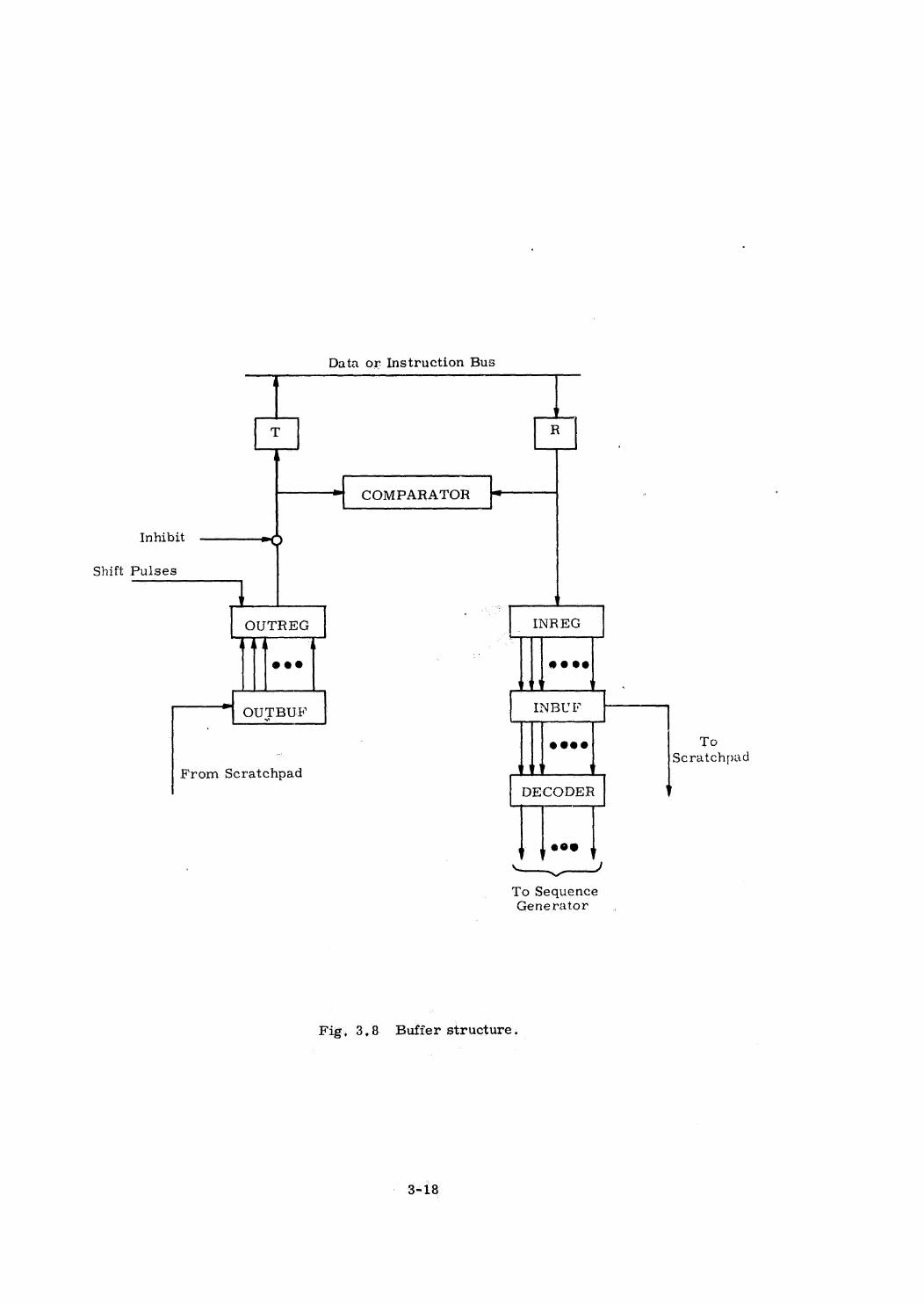
Data or Instruction Bus
fame
4
——
Inhibit ——9
Shift Pulses
= COMPARATOR fo"
OUTREG INREG
e000
OUTBUF
From Scratchpad
INBUF P|
eeee To
Scratchpad L!
DECODER
' eo0@ ’
VS
To SequenceGenerator
Fig, 3.8 Buffer structure. |
3-18
switching. At this rate, the power consumption of 10° bits is ten watts, which
is competitive with magnetics, Essentially the only disadvantage of semi-
conductor memories is that they are still a bird-in-the-bush compared to the
more available magnetics,
Two types of magnetic film memories have been develeped; flat film
memories, whose storage célls are spots of permalloy on thin glass sub-~
strates, ard cylindrical film memories, whose cells are magnetized regions
on permalloy~plated wires. The latter shows the greater promise of utility
in terms of density, and also offers non-destructive readout capability which
offers advantages in reliability. Design work toward a plated wire memory is
reported in the next chapter. Although memories of this type do exist, their
development is not yet considered suitable for the applications discussed here,
The coincident-current core memory is the outstanding candidate for
this application, though the emergence of either the semiconductor memory or
the plated wire memcry could alter the situation, The core memory has very
high density and reliability stemming from vast experience, It is fast enough
for the common memory application, is low in cost, and economical of power.
A variant of the core memory called the laminated ferrite memory is
worth mentioning. Its properties combine good features of the core and plated
wire memories, It is not fully developed, but bears watching.
3.2.2 Page Name Translation
The greatest challenge in memory design for the multiprocessoris in
creating a mechanism for translating from page name to physical address in a
space of time which avoids degradation of performance, The use of an exhaus-
tive list of possible pages is a means of accomplishing this end without any
specialized electronics. It is fast, requiring a single extra memory cycle,
‘but expensive in storage. Its feasibility is a function of thenumberof pages
which will be defined in a complete program assembly, a number whichit is
not desirable to restrict in that so doing would inhibit programming ease,, This
technique would be useful in research, however, as it is the most flexible and
easiest to implement. As an example of the potential of the technique, consider
a 16, 384 word X 40 bit memory in each memory unit, Set aside one-fourth ofthis capacity for paging, and assumethat ten bits are sufficient to locate a
physicalpage within a unit and identify lockout. This gives a page handling
capabilityof 16, 384 page names, a very substantial number for developmental
purposes, : | | | i
3-19
3.3
A more complicated algorithm, still requiring no specialized elec-
tronics and with a much larger page name capacity, is the one described
in Chapter 2. This method uses more than one extra cycle at timesto locate
data, but on a statistical basis, the average is very little in excess of one
cycle,
The alternative to using such schemesis to have a separate associative
memory in each unit with as many words as there are pages in the main memory
and as manybits as are required to contain all page names, probably 15 to 20,
For example, if it is desired to divide the main memory into 256 pages, the
size of the associative memory would be 256 X 15 (or larger) and would output
an eight~bit address code, The cost of such a memory would be high. Various
LSI approaches are possible, but have not yet been implemented. The size of
the memory using the technology of the near future would also beconsiderable.
The most attractive scheme is theons :jiscussed in Chapter 2. Using
a scratch pad memory the size of the one proposed forthe processoror slightly
larger, a page table could be implemented which would handle 512 pages per
memory and a 20-bit-long page name and lockout field. The translation time
would be well under a microsecond in nearly all cases, which would be of little
significance in comparison to the latency of the data bus.
Bus Design
3.3.1 TO Bus
The I/O bus is the interface between the computer and all input and out-
put equipment. Older designs were usually realized by assigning a cable set to
each piece of input and output equipment and often a separate set for each of the
two directions of signal travel, Thus each wire hada preassigned and definite
input end and output end. The problems of power level, bandwidth, and reflec-
tions were localized,
The present application requires a single bus of arbitrary length whose
signal input points are arbitrary and whose signal output points are arbitrary.
Hence the bus may be drivenfrom any single point at any given timeand may be
loaded at any numberof points at that time.
This distributed network must be driven bydrivers which assure that
pulses of optimum shape enter the line and that the pulse exhibit minimum droop
and negligible overshoot and no pre-or post-pulse reflections.
3-20
Transformer selection and turns ratio is based more on thetotal net-
work as a distribution system than upon the ability of the transformer to drive
the load.
loads than those imposed here,
In fact, any of the transformers evaluated would drive much heavier
Transformer coupling allows the voltage across inactive driver trans-~
istors to be a maximum, which makes the collector capacitance a minimum,
and in turn reflects a minimum of capacity into the line, (Fig. 3.13). Minimiz-
ing the shunt capacity minimizes the component of shunt current drawn from
the line. Effectively, the loaded line propagation constant and characteristic
impedance are similiar to those of an unloaded line. The characteristic
= A Zs
y
| ; WL :Zz, ay
which is exactly the impedance of the unloadedline if (We << 1,
impedance 25 is given by
eeewe
Since R is negligible
The complete specification of a transformer is very lengthy and usually
is completed by acceptance testing in the end use circuit.
A group of pulse transformers manufactured by Sprague were selected
for testing. Their characteristics are:
Sprague Type # Breadboard Designation L,(HH) Max.L Max C(pf) Rise Time‘| (nsec)
35Z2021 b,e,f 104 a) 15 8
352.2022 d,g,h 150 2 15. 9
352.2023 a,c 203 wl 16 10 Two impedance levels of line were tested. They were RG58 C/U and
RG62 A/U: Their characteristics are:
MIL No. |V. P.% |Capacity| Nom. Imped. Jacket Dielectric] Center |db/100ftatpf/ft. Ohms O. D. oO. D. Conductor |10mce [30 me
RG58C/U| 65.:9 30.5 50.0 .195 . 116 19x, 0O71TC| 1.6 3.0
RG62A/Ul| 84. 0 13.5 93.0. . 242 . 146 ix,0253CW| .83/1.5
3-21-
The loads on this line must not deteriorate this pulse below a level
which is usable to each of an arbitrary number of other users. Of course, no
load should introduce reflections or remove more than its share of energy from
any pulse.
The total length of the line will be up to fifty feet. Data rate will be up
to 5 megabits per second. Up to twenty drivers and up to twenty reseivers will
load the line.
3.3.1.1 Goals
In addition to the above criteria, the bus must be amenable to an arbit-
rary increase or decrease in (a) length, (b) number of drivers, (c) number of
receivers, (d) position assignment along the line of drivers and receivers.
The pulses at the input to the driver and at the input to each receiver.
shall be standard 0. 1-microsecond duration, positive, 50% duty cycle trains.
The driver circuits, the receiver circuits, and the physical bus itself
shall be constructed of available and proven parts. Monolithic circuits will be
used where applicable.
The design shail be evaluated for its performance under component
degradation. It shall be a further design goal to realize graceful degradation
through the use of redundancy techniques,
3.3.1.2 Design Candidates
The transmission system must meet all of the above criteria. Pulse
pattern sensitivity and reflections are to be avoided. This means that a non-
resonant, wideband, base-band transmission medium operating at its charact-
eristic impedance is required, This terminated transmission line should not be
a radiator nor should it be a receiver of extraneous fields; thus coaxial cable is
chosen,
. Conducted interference is also to be avoided. This implies that all
‘drivers and all receivers interfacing with the line shall exhibit balanced coupling
for three-terminal active devices, e.g. transistors, or that true four-terminal
devices will be used. Thus, transistors or IC's with coupling transformers will
satisfy this requirement for design with conventional components.
Other appealing four-terminal networks are the electro-~optical devices,
It is felt that the use of conventional components at this time is more effective,
Bs‘they have higher and computable reliability, and have transfer value in that
~they canbe used in other parts of the system.
3-22
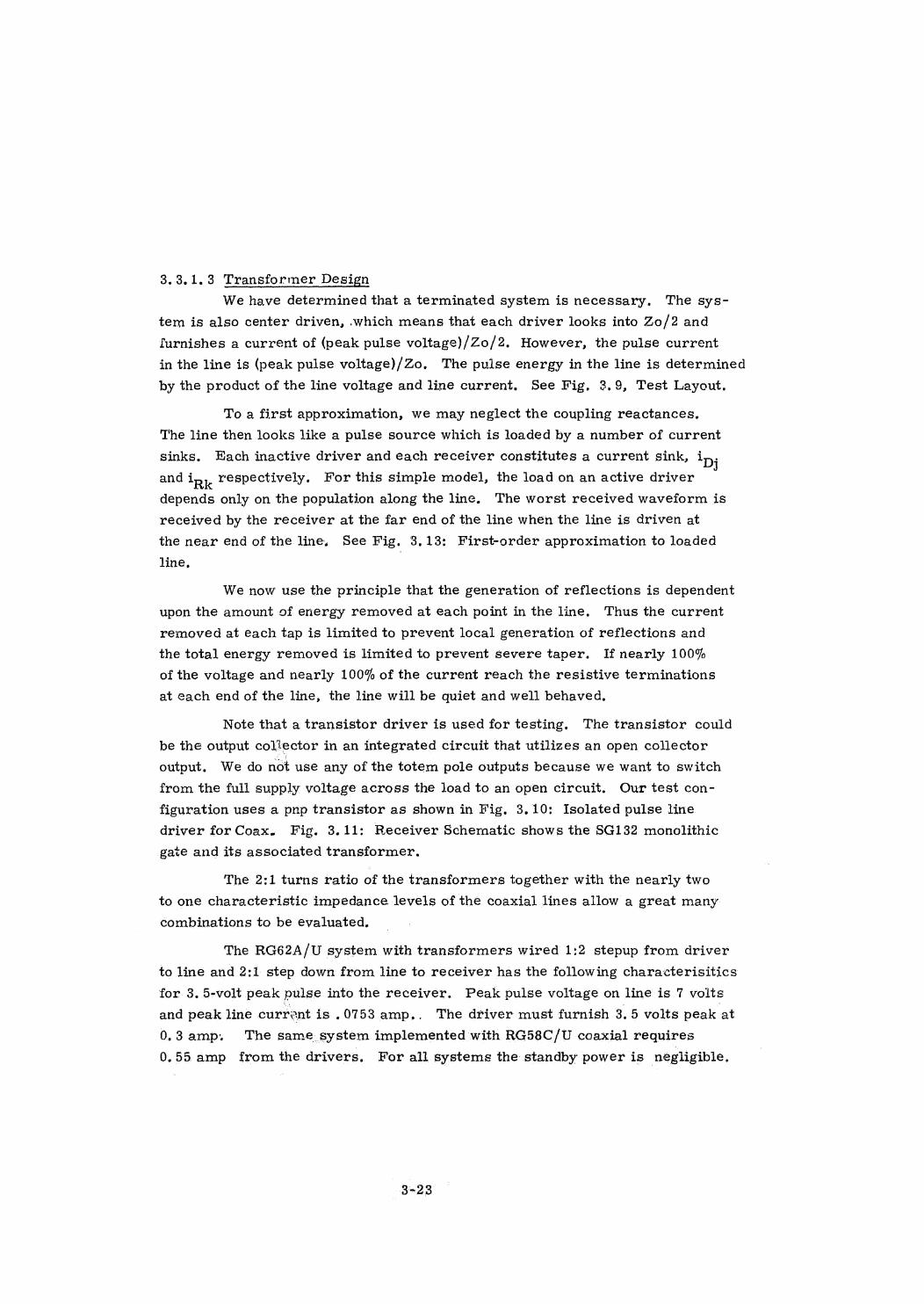
3.3.1.3 Transformer Design
We have determined that a terminated system is necessary, The sys-
tem is also center driven, which means that each driver looks into Zo/2 and
furnishes a current of (peak pulse voltage)/Zo/2. However, the pulse current
in the line is (peak pulse voltage)/Zo. The pulse energyin the line is determined
by the product of the line voltage and line current, See Fig. 3.9, Test Layout.
To a first approximation, we may neglect the coupling reactances,
The line then looks like a pulse source which is loaded by a number of current
sinks. Each inactive driver and each receiver constitutes a current sink, in;
and ink respectively, For this simple model, the load on an active driver
depends only on the population along the line. The worst received waveform is
received by the receiver at the far end of the line when the line is driven at
the near end of the line. See Fig. 3.13: First-order approximation to loaded
line,
We now use the principle that the generation of reflections is dependent
upon the amount of energy removed at each point in the line. Thus the current
removed at each tap is limited to prevent local generation of reflections and
the total energy removed is limited to prevent severe taper. If nearly 100%
of the voltage and nearly 100% of the current reach the resistive terminations
at each end of the line, the line will be quiet and well behaved,
Note that a transistor driver is used for testing, The transistor could
be the output collector in an integrated circuit that utilizes an open collector
output. We do not use any of the totem pole outputs because we want to switch
from the full supply voltage across the load to an open circuit. Our test con-
figuration uses a pnp transistor as shown in Fig, 3.10: Isolated pulse line
driver for Coax. Fig. 3.11: Receiver Schematic shows the 5G132 monolithic
gate and its associated transformer,
The 2:1 turns ratio of the transformers together with the nearly two
to one characteristic impedance levels of the coaxial lines allow a great many
combinations to be evaluated.
The RG62A/U system with transformers wired 1:2 stepup from driver
to line and 2:1 step down from line to receiver has the following characterisitics
for 3. 5-volt peak pulse into the receiver. Peak pulse voltage on line is 7 volts
and peak line current is .0753 amp.. The driver must furnish 3.5 volts peak at
0.3amp. The samesystem implemented with RG58C/U coaxial requires
0.55 amp from the drivers. For all systems thestandby power is negligible.
3-23
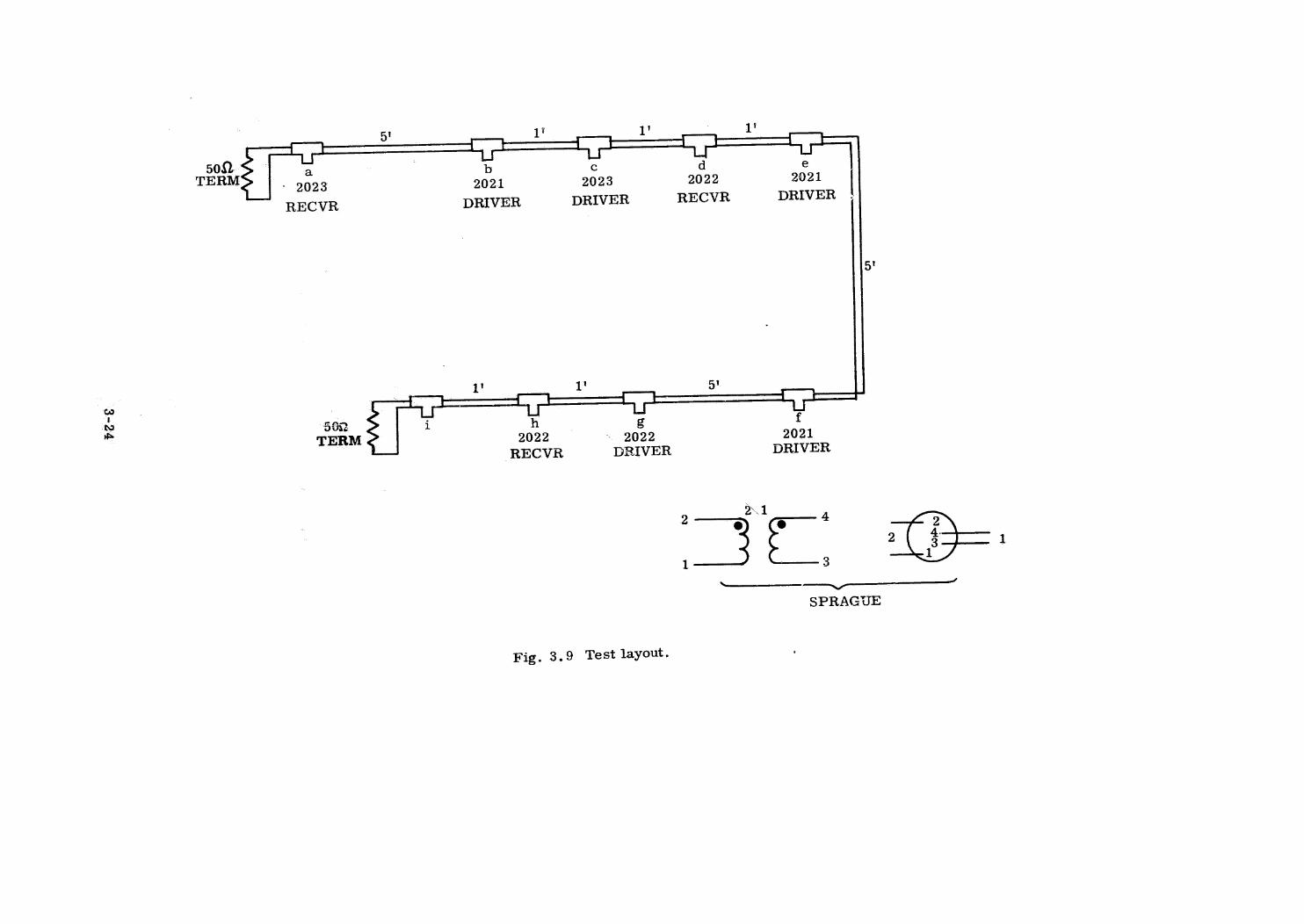
$2-8.
5!
1’1!
li
i lL a
|
to a
|
tT es
|
: LL J
502 Li Ly Li Ly LI
TERM a b c a e
> 2023 2021 2023 2022 2021
RECVR DRIVER DRIVER RECVR DRIVER
5!
1' 1' 5!
i T —_. t a_i 1...—_. {ee
p LS LT Ly Li
SR i h g f
TERM 2022 ~ 2022 2021
RECVR BRIVER DRIVER
12 a) ; 4
2 1
1 3
eee on - ——
4
SPRAGUE
Fig. 3.9 Test layout.
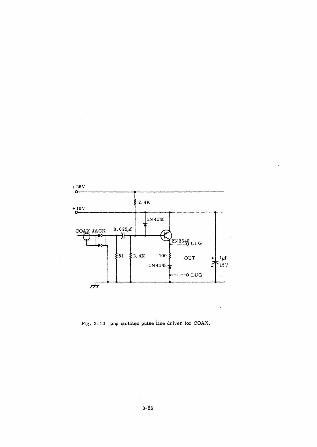
+25V
°
2.4K+10VoO “——
1N 4148
COAX JACK 9. 022uf
;LUG
vl , OUT +) lyf
ST 15V
| pa) LUG
Fig. 3.10 pnp isolated pulse line driver for COAX.
3-25
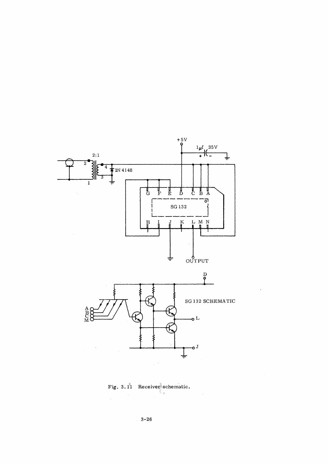
+5V
9 lyf 35V
2:1 4 Ne5 7 ; =
IN 4148
1 —
G F E OD C BA
eeol! SG 132
Dp eeee
H it K LMN
ee OUTPUT
£
8G 132 SCHEMATIC
Fig. 3.14 Receiver! schematic.
. 3-26
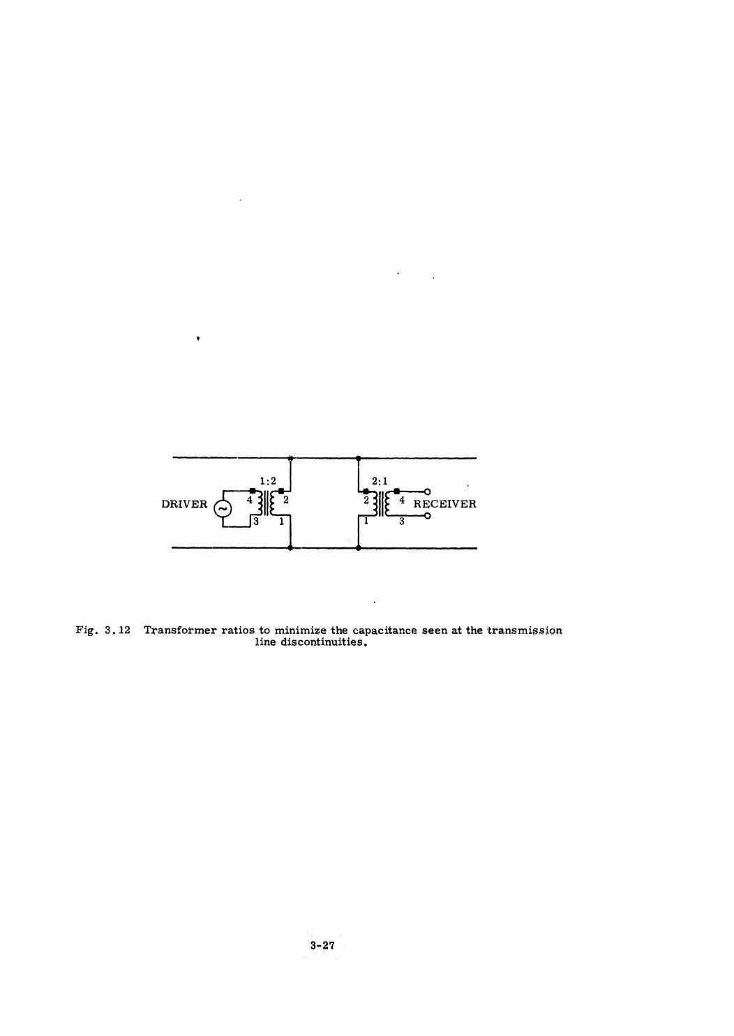
DRIVER
2:1 ;
2 le 4 RECEIVER
i 3
Fig. 3.12 Transformer ratios to minimize the capacitance seen at the transmissionline discontinuities,
3-27
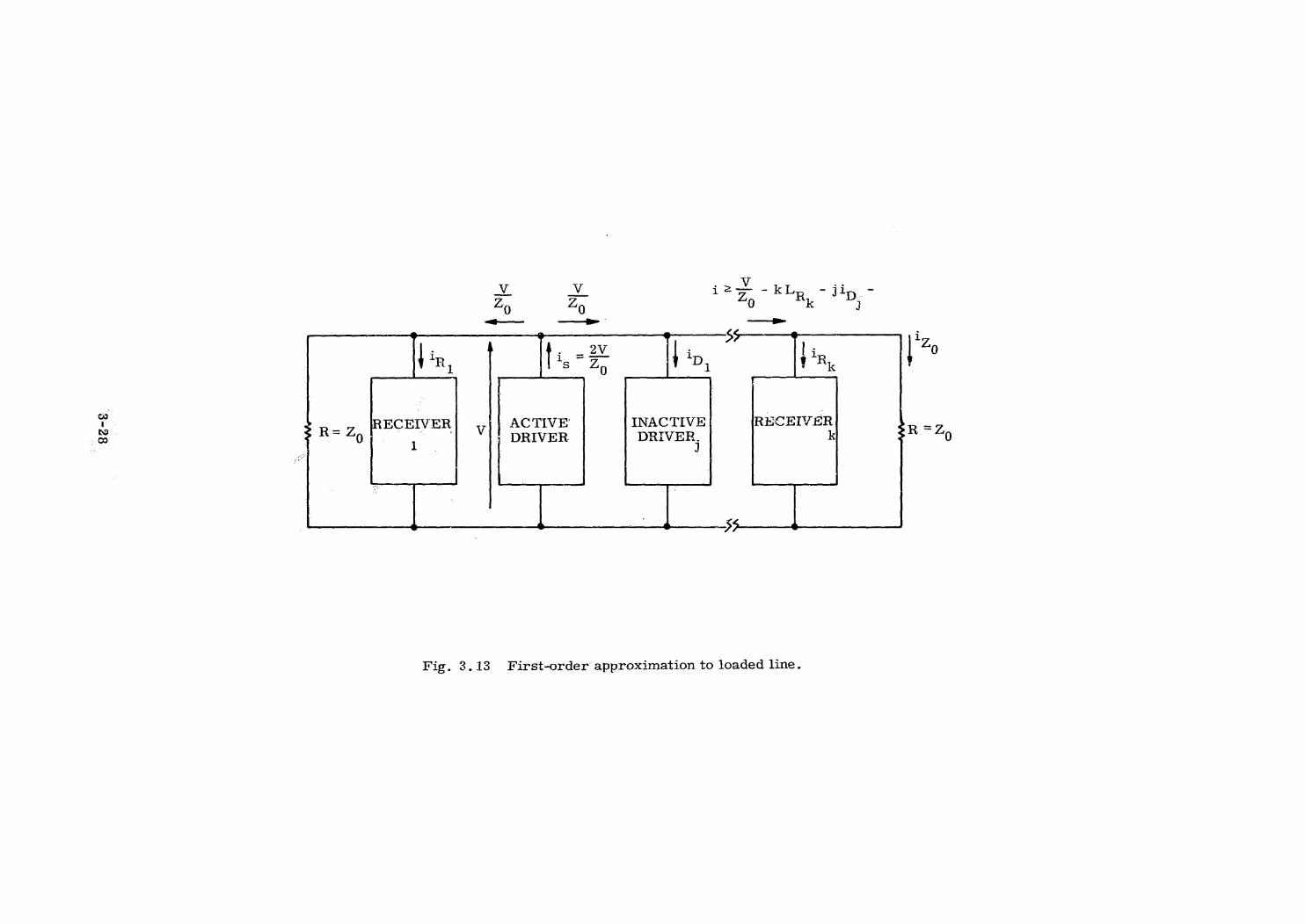
92-8.
wv Vv i25--kL, -ji, -a R D-
49 29 0 k 3—_—— —_—_ —_——
Le *Lo i
\ in | fi - 2V | in Jin | 70
‘1 s 4 1 ' ok
3 p=, (RECEIVER| || ACTIVE INACTIVE RECEIVER Lepee 0 DRIVER DRIVER, k 3R“Zp
| , | — | 55 |
Fig. 3.13 First-order approximation to loaded line.
A sequence of measurements were made with RG58 C/U coaxial cable,
The driver transformers were wired 2:1 step down from driver to line. This
case requires the minimum driver carrent but reflects the maximum capacitance
into the line tap point. The receiver transformers are wired 2:1 step down from
line to receiver. Amplitude degradation is up to 50% for this case. Trans-
formers b and e performed best,
A series of tests were performed with RG62A/U coaxial, Ry doubling
the impedance level (compared to RG58C/U) we can reduce the line power by a
factor of two.
For the case of 2:1 step down transformersfrom the driver to the line
and 2:1 step down transformers from the line to the receivers amplitude degrada-
tion with distance is again 50%,
Another series of tests was performed with RCC2A/U coaxial driven by
transformers which are wired 1:2 step up from driver to lim. The receiver
transformers are wired 2:1 step down from line to receiver, This was by far
the best case, Transformers c and e yielded the best pulse shape everywhere
in the line. No pulse degradation withdistance was measurable for this case
of five drivers, three receivers, and 22 feet of coax, See Pigs, 3.14 and 3.15. .
In general, the voltage and current waveformsthat are inserted into
the line as square pulses suffer degradation with distance down a loadedline.
Rise time degrades until the pulse becomestriangular and further attenuation
yields a lower amplitude triangular pulse,
The best results were obtained with RG62A/U 93-ohm coaxwith alldriver transformers wired 1:2 step up from driver to line and all receivers wired
2:1 step down line to receiver, Transformers c and e were the best coupling
units although the setup was the least sensitive to the particular transformer
used,
A full scale breadboard with all drivers and all receivers in place should
be evaluated. A more accurate transmission model should also be evaluated.
A cornplex value for the characteristic impedance and propagation function should
be derived, Finally, some of.the several other possible ways of driving the.
line should be studied. | |
3.3.2 Data Bus
3.3.2.1 Goals
The data bus will handle 20 mersabits per second RZ data,,-and will be
about four feet in length. It may be loaced by up to 30 drivers and up ta,
30 receivers, “Thus tap“points will be separated by less thananinch on the
3-29
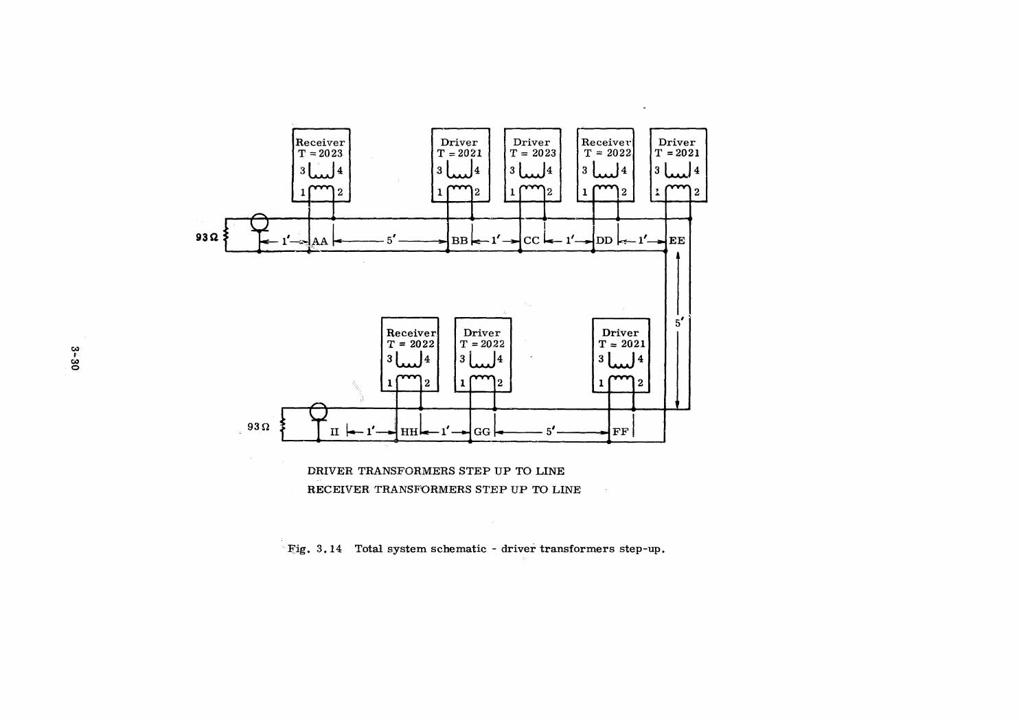
O€7E
e
Receiver Driver Driver Receiver DriverT = 2023 T =2021 T = 2023 T = 2022 T =2021
3[. J 3 |4 3, }4 3 |4 3[.,]41 VY 9 1 vv 9 1 VEY 2 1 VY 2 z vr 2
i> {4 4
932 F hl LL — 5’ ——___»| BB fe— 1—=} CC be— 1/5 DD /-e— 1's» EE+- +
- 4h
5Receiver’ Driver DriverT = 2022 T =2022 T = 2021
3 | Ja 3 | J4 3 | J4
1 vy 2 1 Try 2 1 vv 2
Za 4 tj _t Y
. $
_ 932 F | Tr be 1’el} HH ke 1’ 2] GG | 5)+FF
DRIVER TRANSFORMERS STEP UP TO LINE
RECEIVER TRANSFORMERS STEP UP TO LINE
Fig. 3.14 Total system schematic - driver transformers step-up.
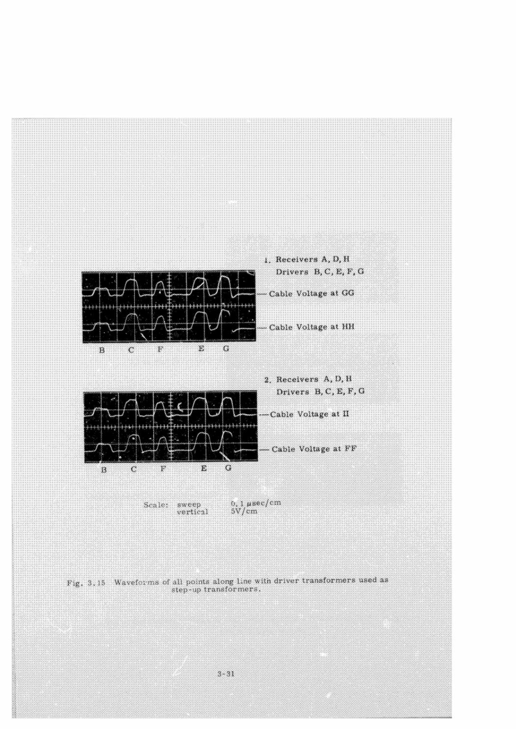
1, Receivers A, D,H
Drivers B,C,E,F,G
m~—~ Cable Voltage at GG
— Cable Voltage at HH
2, Receivers A,D,H
Drivers B,C,E,F,G
-—Cable Voltage at II
ome Cable Voltage at FF
sweep | waec/cmvertical 8V/om
Fig. 3.15 Wavefc:me of all pointe along line with driver transformers used asSlep-up (raneiormers.
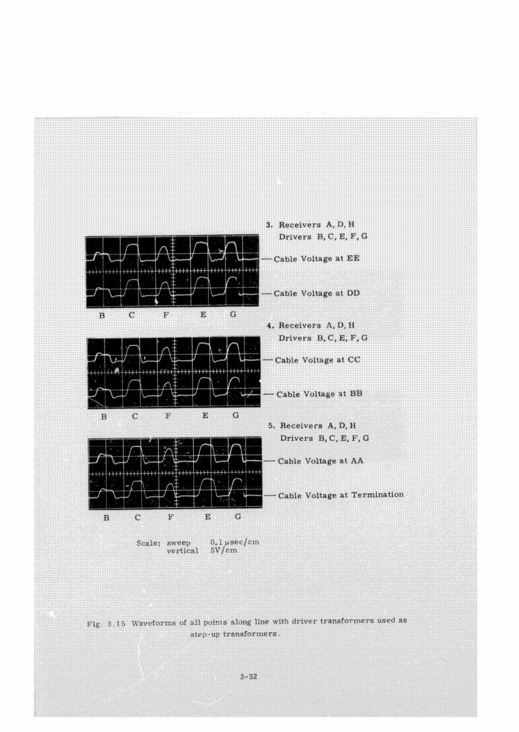
3. Receivers A,D,H
Drivers B,C,E,F,G
—-Cable Voltage at RE
wm Cable Voltage at DD
4, Receivers A,D,H
Drivers B,C,E,F,G
Cable Voltage at CC
~~ Cable Voltage at BB
5. Receivers A, D,H
Drivers 6,C,E,F,G
Mm Cable Voltage at AA
~~ Cable Voltage at Termination
E G
0,l usec/em5V/em
8 1% Waveforms of all points along line with driver transformers used as
step-up transiormers.
average, The physical tightness of the line and the distributed nature of the
constants imply that the total transmission system including drivers and
receivers taust be designed as a unit. (For the I/O bus, driver and receiver
parameters were chosen so that they had a minimum effect upon the line para-
meters. This simplification will not be possible for the data bus).
3.3.2.2 Design Candidates
The bus itself is likely to have to satisfy a peculiar form factor that
satisfies input and output point locations that are determined by system consid-
erations other than bus design. It will be located in a very active electrical
environment so RFI will be a strong consideration. Ground reference will
probably be within a 1/2-volt differential throughout the path. Again, power
and size will not be heavy trade-off items. The pulse performance of the line
will be the dominant design criterion. The electrical requirements will deter-
mine the constants and dimensions of the system, upon which the physical
constants of the materials are specified. Finally, the electrical design must
consider the variations to be expected in production, e, g., thickness and loss
factors. Harmonic analysis of the system will be required.
3.3.2.3 Instruction Bus
The instruction bus will have a bit rate of about 25 megabits per
second, and will be about 4 feet long. There will be up to 15 drivers and 15
receivers.
These requirements will be satisfied by the Data Bus design. Thus
the Instruction Bus will be identical in natureto the data bus.
8-33
wl
ELECTRICAL/MECHANICAL DESIGN
Braid Memory
4,1,1 Review
For several years work has been carried on towards the development
of a read-only memory suitable for spaceborne applications, This development
is called the Braid memory, and progress has been reported in MIT Report B-498
and E-2092, During the contract period covered herein, the effort has been to gain
experience with a larger Braid memorythan has previously been built, and also
to begin designing a new Braid memorywith greater bit density and structural
integrity than before.
4,1,1,1 Advantages of the Braid Memory
The Braid is a wired-in memory whose contents are determined at
manufacture and unchangeable thereafter. High density and low cost cari be
achieved this way, and the potential for turn-around time, i,e., the time required
to generate a Braid once the desired contents are known, is of the order of a few
days. The property of inalterability is a desirable one in some applications,
notably certain programs and most microprograms, where security of data is
of the utmost importance.
Alternatives to a read-only memory (ROM) are read-write memories
(RWM) and non-destructive readout (NDRO) memories. The NDRO memoryis
attractive from the viewpoint of turn-around, as it can be loaded from the com-
puter or the GSE, Its principal disadvantages are its low density and high cost.
The future prospects of the NDRO memory are good, first with plated wire and
later with semiconductors. For the present and immediate future, however,
the ROM is a more satisfactory device in many applications. The RWM is a com-
promise in size and cost, but its security is low, and it is often unsatisfactory
for that reason alone,
4.1.1.2 Fabrication
The reason for the fast turn-around potential of the Braid memory is
the method of manufacture in which information is stored by configuring wires
with a loom, potting the wires, and adding transformer cores, sense amplifiers
and drive circuits. Over four thousand wires are used in the latest Braid.
memory. Drive circuits select one of these by passinga current of tens-of
_ milliamperes through it. The wire optionally threads or does notthread each
of 256 transformers whose secondary windings are sensed, The primary cur-
rent causes the subset of the 256 sense circuits whose transformers are threaded |
by this wire to turn on. oO | :
A-1.-
The loom handles 256 wires, and makes one transformeroption selection
for all 256 in about 16 seconds. The weaving rate can thus be said to be 16 bits
per second. Extra time is required to terminate the wires at the beginning and
end of every "pass" of 256 selections, resulting in a lower bit writing rate.
Both the weaving and the terminating speeds stand to be improved such that an
overall rate of about ten bits per second is feasible, At this rate, a million-bit
Braid can be fabricated in a little over a day.
4,1,1,.3 Electrical Properties
Driving a current through a selected wire and sensing whether the wire
passes through a transformer core has various pitfalls owing to the presence of
parasitic circuits in memories of large size. Capacitance from one wire to
another is the principal source of trouble, and becauseof it there is a limitation
on speed that becomes more severe with increasing size.
The most economical driving circuits, according to conventional cost
assessments, are double-ended drivers with diode isolation of each wire, This
proves to be disadvantageous with respect to speed, and single-ended drivers,
of which one per line is required, are being considered for the next design. Since
termination is a relatively large part of Braid fabrication, it may well develop
that the cost of a transistor per line is proportionally very little more than the
cost of a diode per line, thus permitting a large speed improvement to be made
at little cost.
Sensing in Braid memories has been done by RTL NOR gates driven by
30-turn secondary windings. This report describes two new sense techniques,
one using a 60-turn secondary winding, the other using a secondary of just a few
turns, The remainder of section 4,1 treats our experience with weaving and
testing a 279pit Braid (1, 048, 576 bits) and our studies for a new high-speed,
high~density Braiil memory design.
4.1.2 Design of the Megabit Braid Memory
The megabit braid memory was conceived and designed for two basic
reasons. Thefirst was to test the feasibility of packaging over one million bits
ina single package. The second wasto facilitate morerapid construction and
to test the manufacturing techniques by which such a package could be built. One
of the main problems in the manufacture of such a braid was the further develop-
ment of termination techniques, mainly at the diode end of the word lines, which
previously had constituted the largest time-consuming part of braid manufacture.
Other reasons for the development of such a braid were to lower the total power
consumption of the associated electronics and to test new sensing circuits,
4-20
A new "boat" (section that contains the potted braid) and a matching
electronics frame were designed for the megabit braid. The actual braiding
area remained the same in length and width but increased 50%in thickness to
accommodate the 100% increase in number of wires. The overall dimensions
of the new package were governed by the area necessitated by the new diode
board design; the complete package measure 15-7/8"' X14-1/2" X 2", Wo specific
effort was made to increase the storage density; however, the density of the new
package increased slightly over that of the previous package.
4.1.2.1 Termination
Since the initial termination of wires to separate diodes took the majority
of time in the manufacture of a braid, considerable time and effort were spent
investigating mass termination procedures,
Previously, wires were terminated to diodes manually, one at a time,
The loom selected the wires to be terminated to a specific diode board and the
operator would pick one wire at a time, in order, make a single turn around the
corresponding dicde lead, then solder. This was a rather long and tedious pro-
cess. Termination of the 256 wires necessary for a single pass took over two
hours.
In the megabit braid a mass termination method was tried with very
good results, The average terminating time per pass dropped to approximately
forty minutes, For this procedurea new diode boardwas designed and new
reeds were installed on the loom. The new diode boards are slotted on .100"
centers, andthe pitch on the new reeds is .025", Every fourthwire is selected for
terminations, A high-temperature solderpot was installed on a lift table in the
appropriate area under the loom.
The mass soldering method proceeds as follows: the loom makes a
"pick" of the wires to be terminated, and thesewires are then "combed"into
their respective slots of the diode board. The diode board is then placed in a
holding fixture and the solder pot control circuit is activated. The solder pot
rises to a predetermined height and remains there for a controlled length of
time while soldering the wires to pads on the diode board, and then returns to
its orginal position. Each diode board contains 64 diodes; therefore, four diode
boards are used per pass, and a total of 64 boards are necessary for the com-
plete megabit braid. . : |
4-3
Probably the biggest problem of this mass termination method lies in
the expense and manufacturing problems associated with the diode boards. The
boards are double-sided printed circuit boards with a series of plated-through
slots .030" wide on .100" centers. it is believed that a one-sided printed cir-
cuit board would suffice, and that, with some more refinement and development
of combing and terminating techniques, even the slots may be eliminated.
4,1,2,2 Weaving the Braid
The actual weaving was performed in the same manneras in the previous
2048-wire braid. Since the capacity of the braid was to be doubled, there were
16 instead of 8 passes made with the loom. The average time per pass for the
actual weaving process including removal of the temporary storage rods was
approximately 1-1/4 hours.
In the preliminary continuity check 130 word-lines were found to be open.
An analysis of these reduced the number of actual faults (broken wires) to 68,
The remaining errors proved to be due to poor solder termination, primarily at
the receiver end of the braid, and diodes having been inserted in the diode boar‘s
with the wrong polarity. A closer check of the broken wires revealed that the |
breakage had occurred mainly in a particular area of the braid where only the
first "pass" contained information with a few "ones". All other wires were
"zeros" in this bit position. The actual breakage was caused by the dropping of
the temporary separator rods onto these few wires andliterally chopping them
up. Normally these separator rods are cushioned by the build-up of wires from
successive passes.
A correction tape was made and a correction pass woven into the braid.
Plugs were inserted into the separator rods to keep them from falling to the
bottom of the boat when the bars were removed, (The bars are temporary fix-
tures which fit between the rows of;nails, and are used to keep the weaving of
the braid above the nails.)
4.1.2.3 Driving
In the previous 2048-wire braids both a discrete electronics package and
an integrated-circuit electronics package had been used with very good results.
In the interest of power consumption and to gain better control over the drive
current it was decided to use a combination of these packages in the megabit
braid. |
Integrated circuits such as those used in the previous braid were used
as receivers or bottom switches. These were paralleled two gates to a receiver,
with a total of 128 receivers. | |
A-4.
Discrete components were used as transmitters or top switches, There
are 32 such gates, all of which are driven by a common-current driver. This
was doneto gain better control of the current wave forms, which in turn should
aid in lowering the noise mechanisms within the braid as seen at the sense
amplifiers.
Since the numberof word lines in the megabit braid was twice that of
previous braids, it was expected that the receiver bundle capacitance of the
wire would increase proportionally, This would make it more difficult for a
selected receiver to discharge its word lines. However, by making the organiza-
tion such that the number of transmitters remained the same and only the num-
ber of receivers doubled, no receiver would have to discharge more than 32 lines,
thus minimizing the problem of discharging selected bundles.
The greatest power saving was made in the electronics package by using
low-power DTL to decode the address lines. The total power consumption for
the megabit braid is 12 watts.
4.1.2.4 Sensing
The sensing circuitry involved the greatest electronic change in the
megabit braid. In previous braids a multilayer board provided the sense windings
and-inw-power RTL gates were used as sense amplifiers and inhibit switches,
In the megabit braid discrete components are used for sensing and
inhibiting. A 60+turn winding on a bobbin is recessed into the sense board, The
output of the sense windings is terminated directly to the base of the amplifier
transistor and an inhibiting transistor is placed across the winding ag a means
of shorting the sense output. Bit outputs of the sense amplifiers are connected
together to perform the wired-OR function, and drive an output register of sixteen
J-K flip-flops. The register clock input is used to strobe the amplifier outputs
into the flip-flops, Thus, a buffer and means of storage is incorporated into the
sensing package,
4.1.2.5 Testing
In testing the braid several problems werefound. The first was.a single
word line which had, by yet undetermined means, become shorted to the frame,
This wire was isolated and a separate wire run through the parity positions so
that other checks might be made. -
In cycling through the 65, 536 word braidand testing for parity, 10 errors
were found, This is an error percentage of . 01 5%. It was also found that these
10 errors occurred on only three word lines. .
4-5.
The first three of these errors appeared on one word line and were
due to omissions on the correction tape.
The next errors, in four successive words, were also attributed to a
single word line that was woven during the correction pass. However, unlike
the first errors, tne information was found to be correct on the tape. In weaving
the correction pass only one-fourth of the wires were used and the remaining
wires were left in the "zero" position. It is probable that the wire containing
the 4rrors was caught in the unused wires such that wire separation was effected
after the error-detection switches. These errors are not attributable to the loom
and probably would not have occurred had the unused wires been kept in the "one"
position (as is done when terminations are made).
The’ last errors were a dropped "one" in three successive words on the
same word line, These errors occurred during the initial weaving, and, since
the information on the tape was found to be correct, they were attributed to the
loom. Thus, it might be said that the loom had an undetected-error rate of 3 in
1, 048, 576 bits or less than , 0003%.,
Although an error-checking system is incorporated in the loom electronics,
a mechanical mode of failure has been found that might deceive this check. The
check switches provide positive indications for the "zero" position of each wire;
that is, the switch is activated by a wire in the full zero position. Thus the
switches do not distinguish between partially-raised and fully-raised wires,
although a partially-raised wire may be below the shuttle and will ultimately be
separated, undetected, into the zero group.
There are two possible methods of eliminating undetected loom errors:
first, by eliminating the mechanismby which a mechanical "hang-up" or partial
separation may occur; andsecond, by installinj another set of error-detection
switches to provide indication of the fully-raised ("one") position,
It should be noted that it is possible that the 4 errors in the second
group were caused by the same mechanism that caused the last group of errors.
‘It is also possible that all errors not due to tape errors could have been caused
by the operator missing a wire when inserting the temporary rods. However,
this is quite unlikely as the operatorwould have had to miss the same wire on
three or four successive picks. This type of error should appear as an individual
error.
Previously developed techniques provide a meansof correctingthese
errors. The offending word lines are disconnected at the transmitter and
receiver ends of the braid and are replacedby new wires woven with the correct
information. If the number of wiresto be corrected or changed‘is small, the
new wires are run jn dy hand; if a significant numberof wires is to be changed,
a correction tape is made up and the new wires are installed with the help of
the loom.
4.1.3 Design of a High Density Braid Memory
The design of a Braid of improved performance and density is currently
in progress. It is based upon the results of some analytical and breadboard
experimental studies of sensing, driving, and density, which are described in
this section.
4.1.3.1 Sensing
4,1.3.1.1 Model
The word-line-core-sense~winding configuration is shown in Fig. 4,1
with its lumped-element circuit model; the model is shown in expanded form in
Fig. 4.2, The flux components of interest are the primary leakage flux 901
the secondary leakage flux $)5, and the mutal flux tun * $y consists of all flux
that links both the word-line and the sensecoil,
If 9an is assumed to be confined to the core,
a age ROSE (hy - Ni)
where
Hy = permeability of free space = 47 10°" H/m = 31.9 nH/in.
HR initial permeability of core material,
Acs : cross-sectional area of magnetic path.
(0) = mean magnetic path length.
Setting i, = 0, the magnétizing inductance La is given by
Ls = ®m_ _ MotR Acs” (4-1)“Tat Tp w
and is hence the inductance that would be measured ifa single turn were placed
on the core with perfect coupling.
4-7
7 Ly»
ooT1 (IDEAL)
iy
Fig. 4,1 Sense position transformer.
4-3
Ife oo,| d 1
The primary leakage inductance Lp, accounts for flux that links only
the word-line ab (¢ap and is somewhat higher than the inductance of segment
ab in the absence of the core. Note that if the word line is driven by a current
source, Loy has no effect whatsoever on sensing.
igo is the secondary (or primary-to-secondary) leakage inductance and
is somewhat greater than the inductance of the sensing coil in free space because
of partial flux linkage with the core. Ly 2 is strongly dependent upon winding
geometry and numberof turns, If altering the numberof turns does not substaiitial-
ly affect the geometry of the coil, Ly. varies as N*; if the winding geometry issuch that each added turn encloses a largerarea than tie previous turn (e.g.,
aspiral), Lo» varies with a power of N greater than 2.
The resistance ry accounts for losses within the core and to some extent
for the variation of losses with frequency and peak flyx density. The value of ro
for a given application can be computed from manufacturer's data of core loss
(typically in mw/em® or watts/lb) versus peak flux density and frequency.
For a single-turn perfectly coupled winding driven by a voltage source
e(t)= E sin wt, the flux density is giverby |
Bt)= = elt) dt= - Ecos wt 2. Boos wtcs * “os
and the power dissipated is
nw| a (Bo a.)
c re
The core-loss resistance is then
Aw
#7 wi? Aas.al naereuand ohms (4-3)
aP/V) (0)
where
“a . 2B = peak flux density, webers/m
w = angular frequency
Aas = cross~sectional area, m*
(2) = mean magnetic path length, m.
(P/V), core loss, watts/m®,
4-9
The core loss represented by the model (Eq. 4~2) is seen to increase as the
square of both the peak flux density and frequency. Since this is not strictly
the case with realistic ferrites, the core-loss resistance for the same core
may vary an order of magnitude depending upon application. Ferrite cores
having shapes and characteristics useful for braid application exhibit a single-
turn ry of about 2-5 ohms, which can often be shown to have negligible effect.
4,1.3.1.2 Sensing Devices
4.1.3.1.2.1 Pesistive Load
The equivalent circuit is made manageable for the following analyses
by assuming zero core loss (rem o) and negligible capacitance across the sense
winding. Capacitance is treated as part ofthe load, It is also assumed that
secondary leakage inductance Loo varies as nw such that Ling = nN? Loo: All
components of the model are referred to the sense-coil output in Fig. 4.3.
Clearly, if the magnetizing current in is kept small by some means, an ideal
"current" transformer results with i, = ip/N-
If a step drive current of magnitude I is applied, the output voltage and
current are given by
I ts(t) = —N— exp - BE (4-4)
1+ —° wey (1+ —£2m \ LT
m mM
and
V(t) = R, itt) (4-4a)
At atime ts after the start of the drive current step, the output of the
sense amplifier is strobed with a zero-width pulse, and the sense winding output
must not have decayed below a threshold (V_.p or ign) at this time. (Practically,
t. is chosen as the time of the trailing edge of a real strobe pulse.) The strobe
time is determined by noise mechanisms in the braid harness itself; in typical
braid configurations the output should hold up:ior more than 100 nanoseconds.
The drive current magnitude necessary to produce int at ts is, from equation 4, 4,
L t_R
I=N (: + =) ior exp
—
f+
—__
m | ON (Ly + Lo)
4-10
2
Wo pe —et W WORD-LINES
W3 pwmL
ept
n. =0 for stored 0
L | 1
}....2../741 | hg I n, =1 for stored 1weeb. ake|
-1
“Wi “L1 | nN |~—|
—-
IDEAL W+1 WINDING
LJ | TRANSFORMER
N7L | Wrim '
Nr | i=0
p
----------
SENSE WINDING &TERMINALS
Fig, 4.2 Expanded model of sense position transformer.
4-11
Differentiating with respect to N and setting the result equal to zero,
it is found that the required word-line current is minimized for a specific
number of coil turns N°:
(4-5)
for which
t_ R L
lzipp 2 ~~ ( + i) (4-6)m m
or
Log teIv T 2 (1+ +) ROL (4-6a)
m. Lm
Maximum sensitivity is hence achieved by using as an amplifier either
a voltage-sensitive device with high input impedance or a current-sensitive
device with low input impedance.
The best sensitivity that can be achieved using a voltageesensitive
device is limited by the maximum number of sense-winding turns that can be
tolerated considering density and winding capacitance, Practical sense windings
are presently limited by both considerations to a few-hundred turns, If the
sensing turns are thus fixed it is found that there exists an optimum value of
load impedance Ry:
for which
4-12
A value of Re lower than Rio decreases the overall amplitude of the
output voltage, while the output collapses too quickly if Ry is greater than RyO°
If practical values are assumed (Nnax = 150T, Lin = 0,2éM h, Loo = 30 nH,
Vor = 50 mV, ts = 0.3, sec), it appears that the word-line current need be only
1,36 milliamperes if the sense amplifier input impedance is adjusted to about
17 K82, However, the response will be extremely sluggish due to winding and
parasitic capacitances. If 5 pF is assumed to appear at the sense-winding
terminals, the natural resonant frequency is about one megahertz. Recovery
time is, at best, on the order of a microsecond.
The most attractive sensing device for this application is an amplifier
which produces an output proportional to input current and has essentially zero
input impedance, It is apparent from equations 4-5 and 4-6 that such a device
allows the use of small drive currents while using sense windings of but a few
turns, hence keeping reflected reactances small and allowing higher speeds.
The implementation of such a device using a high-gain high-speed
amplifier with negative feedback is shown in Fig. 4.4. The input impedance
approaches zero since node a is a virtual ground, and the gain of the amplifier
However, the cost of(r= V /i,) is equal to the feedback resistor Rout F*
powering a few hundred such amplifiers in conventional form is large; a braid
memory utilizing 256 amplifiers in commercially available form will dissipate
15 to 30 watts in the sensing circuitry alone unless some form of power switch-
ing is employed.
A low impedance amplifier may be realized more economically by
loading the sense coil with a common basetransistor stage as shown in Fig. 4.5.
The winding current is reproduced at the collector(s), with almost complete
isolation, while an impedanceon the order of 25-50 ohmsis presented to the
winding, The differential configuration (with its attendant balance problemsif
unipolar signals are to be sensed) eliminates the coupling or bypass capacitor
necessary with the single-ended configuration. The stage is biased so that the
quiescentcollector (output) voltage is nominally 0 VDC;and thewinding polarity
is such that positive word-line current produces a positive output voltage excur-
sion. The stage is capable of driving logic directly, although performanceis
improved considerably. by the addition of an emitter-follower output stage.
If bias current is set properly and a sufficiently fast transistor is used,
. theinput impedance is primarily a resistance of hay ohms. The sense-winding
output current is then given by equation 4-4 with Ry = hey ~The speed of the
sense amplifier is taken into account by assuminga lumped capacitance Cy from
the collector of the common basestage to groundas shownin Fig. 4. 5a.
| 4-13
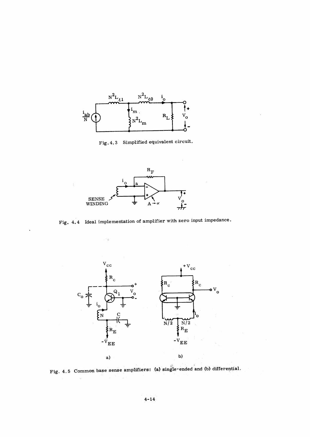
Ny No toi +
"ab a“ R :N 2 L °
SENSE T .WINDING
|
nd
a) b)
Fig. 4.5 Common base sense amplifiers: (a) single-ended ‘and (b) differential.
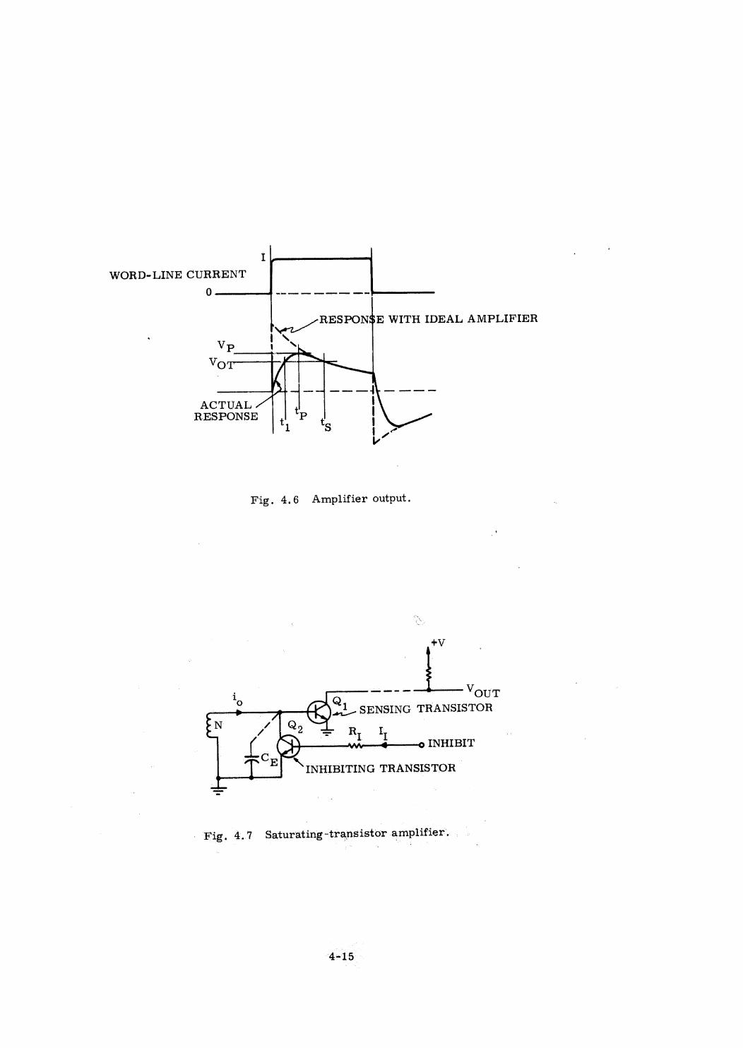
I
WORD-LINE CURRENT
0 eeee
RESee PONSE WITH IDEAL AMPLIFIER
}oNVp \ NX
VYor-——"T7
j~—4—— — ff — —— -
ACTUAL 1) t |
RESPONSE
|
,| 'P |t |
V*
Fig. 4.6 Amplifier output.
+V
—a- VoutSENSING TRANSISTOR
WN o INHIBIT
INHIBITING TRANSISTOR
| Fig. 4.7 Saturating-transistor amplifier.
4-15
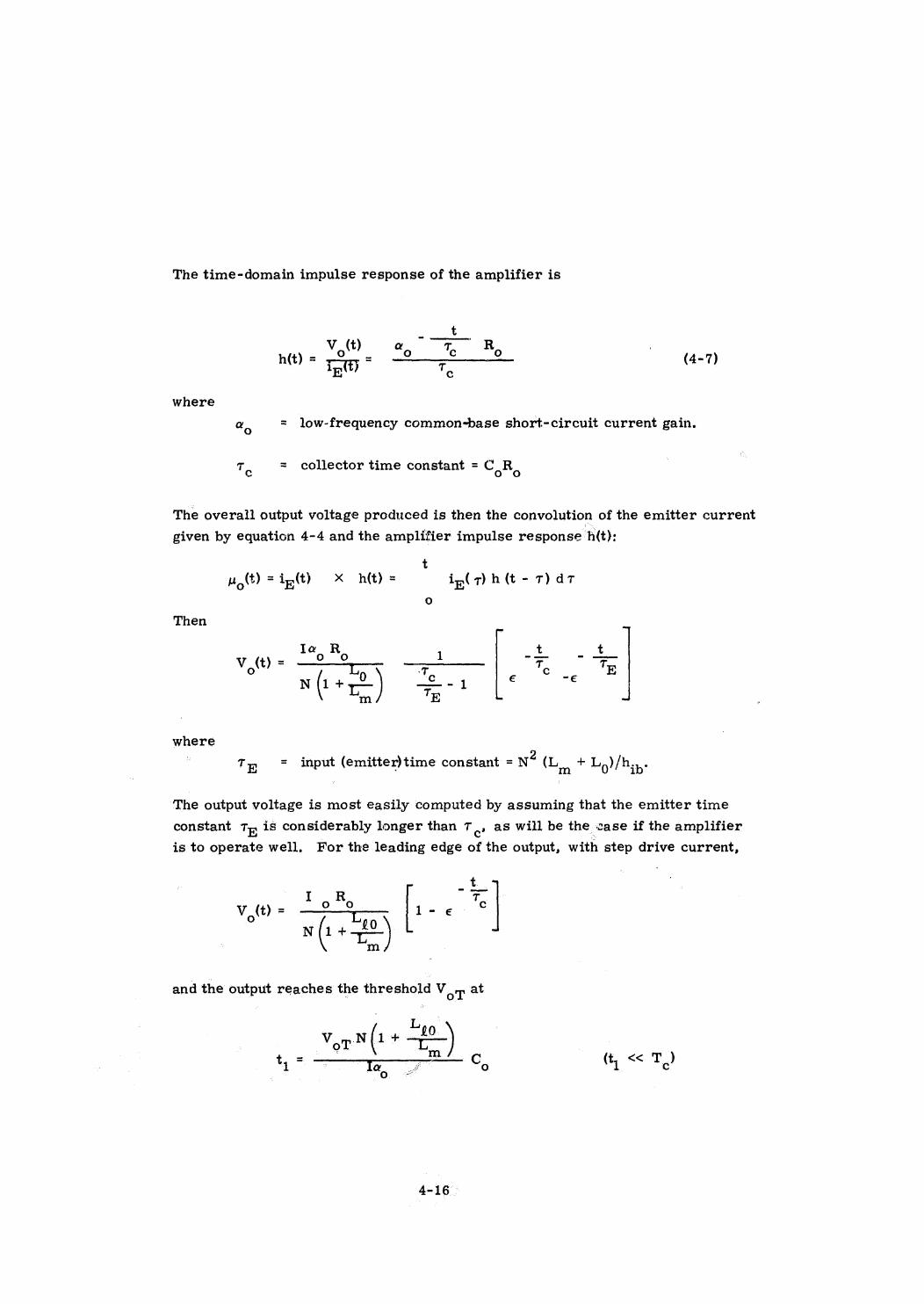
The time-domain impulse responseof the amplifier is
tV(t a T R ;
h(t) = ro = Se (4-7)E c
where
a, = low-frequency common-base short-circuit current gain.
To = collector time constant = CUR°
The overall output voltage produced is then the convolution of the emitter current
given by equation 4-4 and the amplifier impulse response h(t):
tuo(t) = iptt) x hit) = ip( a) h(t - 7) dT
oO
Then
Te R t t~ Oo oO 1 -— -
V(t) = Tp 7 To TEN (1 + 2) = -1 € “€
m TE
where| oa . . _ neTy = input (emitter)time constant = N“ (L_ + Lo)/h,-
The output voltage is most easily computed by assuming that the emitter time
constant Tp is considerably longer than TQ» as will be thease if the amplifier
is to operate well. For the leading edge of the output, with step drive current,
20
m
ta
v(t) = mB) E . °
and the output reaches the threshold Vor at
vV_~N(1+ P20.or N(1 pe
them 1a. Cy (t, << T)
4-16
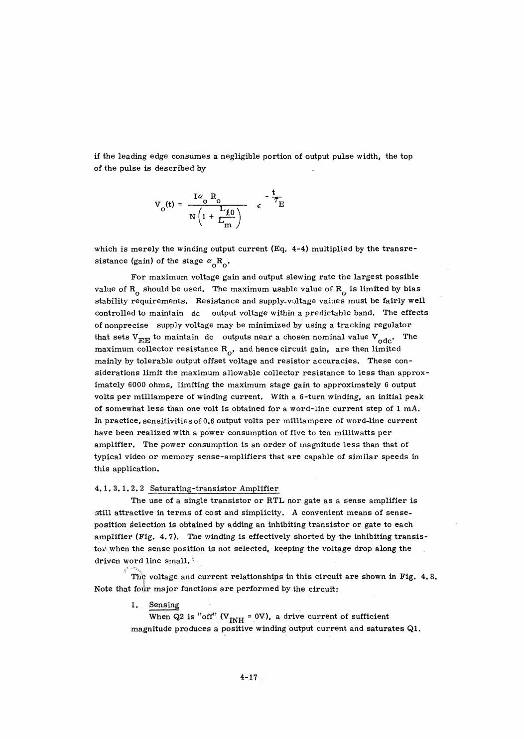
if the leading edge consumes a negligible portion of output pulse width, the top
of the pulse is described by
le R -4-vi) = —25— « E
°o £0x (+ eel)m
which is merely the winding output current (Eq. 4-4) multiplied by the transre-
sistance (gain) of the stage @oR.
For maximum voltage gain and output slewing rate the largest possible
value of R, should be used, The maximum usable value of R° is limited by bias
stability requirements. Resistance and supply.vultage vaines must be fairly well
controlled to maintain dc output voltage within a predictable band. The effects
of nonprecise supply voltage may be minimized by using a tracking regulator
that sets VER to maintain de outputs near a chosen nominal value Vode’ The
maximum collector resistance Ro and hence circuit gain, are then limited
mainly by tolerable output offset voltage and resistor accuracies, These con-
siderations limit the maximum allowable collector resistanceto less than approx-
imately 6000 ohms, limiting the maximum stage gain to approximately 6 output
volts per milliampere of winding current, With a 6-turn winding, an initial peak
of somewhat less than one volt is obtained for a word-line current step of 1 mA.
In practice, sensitivities of 0.6 output volts per milliampere of word-line current
have been realized with a power consumption of five to ten milliwatts per
amplifier. The power consumption is an order of magnitude less than that of
typical video or memory sense-amplifiers that are capable of similar speeds in
this application.
4,1,.3.1,2.2 Saturating-transistor Amplifier
The use of a single transistor or RTL nor gate as a sense amplifier is
still attractive in terms of cost and simplicity. A convenient means of sense-
position selection is obtained by adding an inhibiting transistor or gate to each
amplifier (Fig. 4.7), The winding is effectively shorted by the inhibiting transis-
tos when the sense position is not selected, keeping the voltage drop along the
driven word line small, ‘.f Ss. ; . .
The voltage and current relationships in this circuit are shown in Fig. 4.8.
Note that four major functions are performed by the circuit:
1. Sensing .
When Q2 is "off" (V9), = 0V), a drive currentof sufficientmagnitude producesa positive winding output current and saturates Qi,
4-17
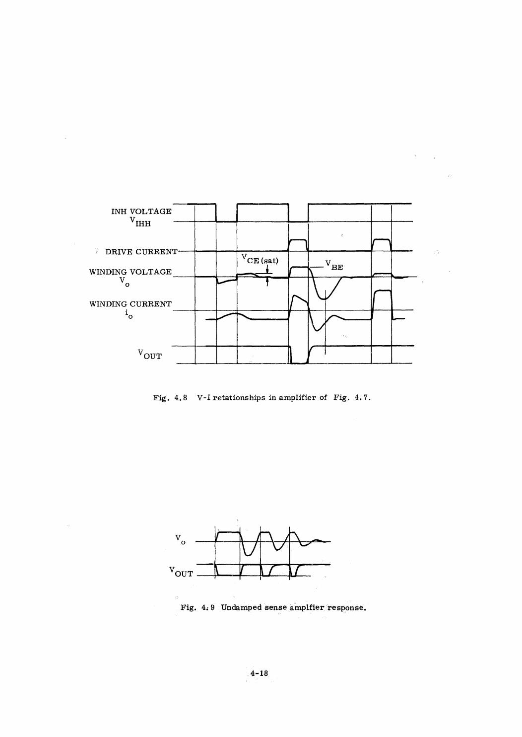
INH VOLTAGE
VinH
DRIVE CURRENT
WINDING VOLTAGE
Vvo
WINDING CURRENT
*o
VCH (sat) y\ BE _
YS
OUT
Fig. 4.8 V-Iretationships in amplifier of Fig. 4.7.
[VY Lf.
Fig. 4:9 Undamped sense amplifier response,
4-18
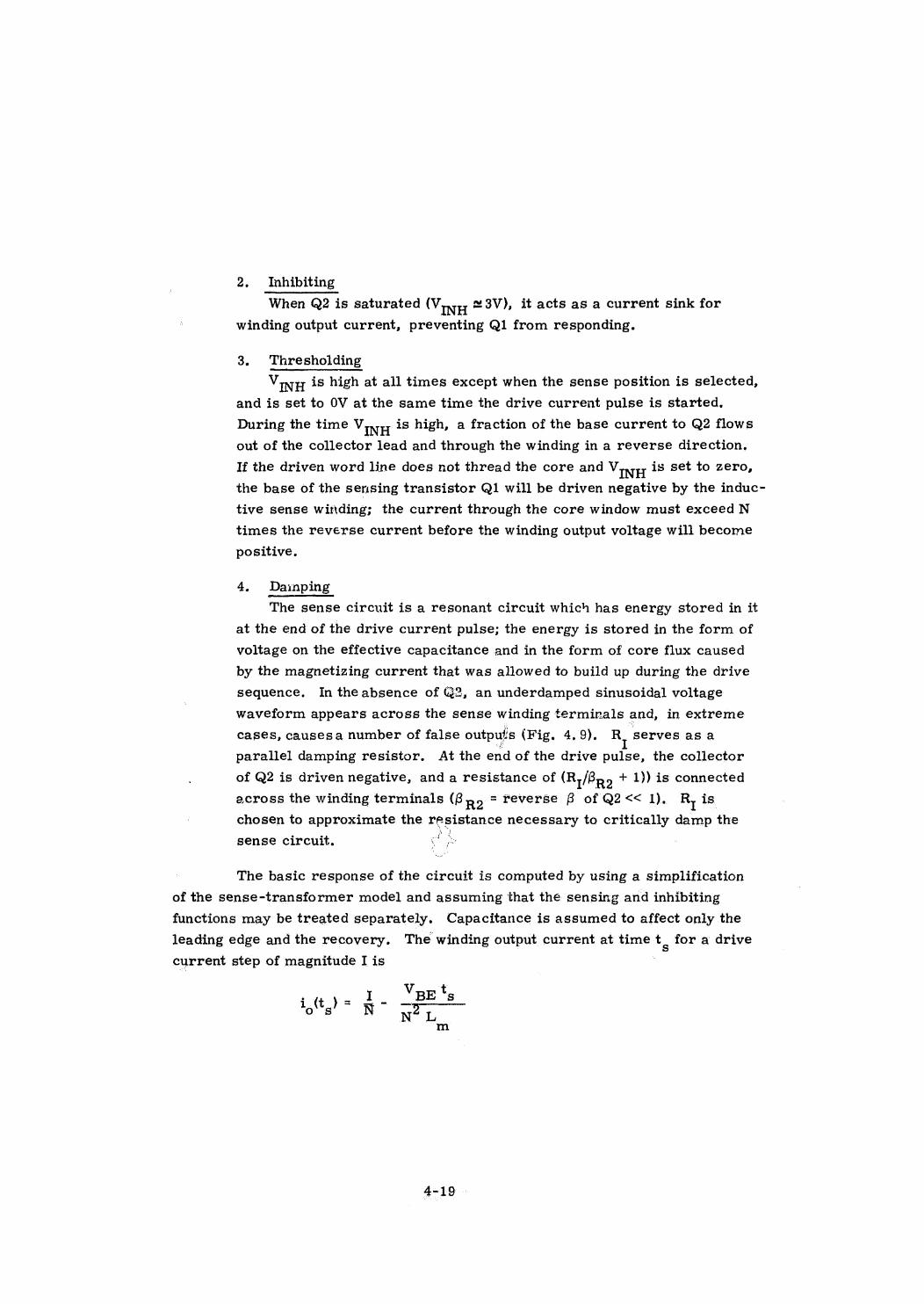
2. Inhibiting
When Q2 is saturated (Ving ~3V), it acts as a current sink for
winding output current, preventing Q1 from responding.
3. Thresholding
Ving is high at all times except when the sense position is selected,
and is set to 0V at the same time the drive current pulse is started.
During the time Vina is high, a fraction of the base current to Q2 flows
out of the collector lead and through the winding in a reverse direction.
If the driven word line does not thread the core and Vini is set to zero,
the base of the sensing transistor Q1 will be driven negative by the induc-
tive sense winding; the current through the core window must exceed N
times the reverse current before the winding output voltage will become
positive.
4, Dainping
The sense circuit is a resonant circuit which has energy stored in it
at the end of the drive current pulse; the energy is stored in the form of
voltage on the effective capacitance and in the form of core flux caused
by the magnetizing current that was allowedto build up during the drive
sequence, In theabsence of @2, an underdamped sinusoidal voltage
waveform appears across the sense winding terminals and, in extreme
cases, causesa numberoffalse outputs (Fig. 4.9). R, serves asa
parallel damping resistor, At the end of the drive pulse, the collector
of Q2 is driven negative, and a resistance of (Ry/Bpe + 1)) is connected
across the winding terminals (8 R2 = reverse 6 of Q2<< 1), R, isI
chosen to approximate the resistance necessary to critically damp theae
sense circuit. oef~
The basic response of the circuit is computed by using a simplification
of the sense-transformer model and assuming that the sensing and inhibiting
functions may be treated separately. Capacitance is assumed to affect only the
leading edge and the recovery. Thewinding output current at time t. for a drive
current step of magnitude I is
s . Iitt) = yo a
4-19 —
For a given minimum sense output current of io at toe I must be greater
than
Iis minimized for
and is
Choosing i, = 0,1 mA, ts =0.2 ywsec, Ver =0.7V, and La = 0.3 wH, we find
that word-line current is minimized for a sense winding of 68 turns and that
13.7 milliamperes of word-4ine current is necessary to hold the sensing transistor
in saturation. The effect of core loss, which was previously neglected, may be
estimated by assuming ro? 2 ohms and adding to I, a current ion, = Vpp/N roe smA.
The effective parallel resistance necessary to critically damp the circuit is found
to be approximately 6K ohms, while the core loss presents an effective resistance
of approximately9K ohms; hencethe resistor to the base of Q2 should be approxi-
mately 18K,
A lower bound is set on the value of Vinu to preserve the inhibiting
function of Q2. If the worst-case discharge current that may occur is 100 mA,
then Q2 must accept a collector current of 1.47 mA while remaining saturated;
if B, = 20, then the minimum base current is 73.5 uA, implying that Vinn must
: be larger than approximately 2 volts. Setting Ving at 3 volts results in a base
current of 128 yA of which, say, 60 wA will flow as reverse current through the
sénse winding, producing the thresholding effect described above, This raises
the required minimum word-line current to 22.5 mA. |
The delay #ime associated with a "one"! output is computed to be approxi-
mately 50 nsec, while the recovery time is approximately 380 nsec.
4,1.3.1.2.3 FET Multiplexer
. A sense-signal multiplexer using field effect transistors as high-speed
analog switches is illustrated in Fig. 4.10. Here, some of the speed and
sensitivity achievable with low impedance amplifiers is traded for a substantial
° improvement in sense-position simplicity and overall power‘consumption while
4-20
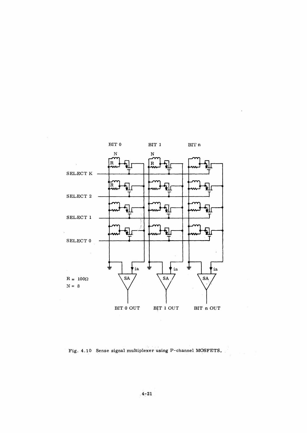
BIT 0 BIT 1 BIT n
SELECT K
SELECT 2
SELECT 1
SELECT 0_
R= 1009
N= 8 BIT 0 OUT BIT 1 OUT BIT n OUT
Fig. 4.10 Sense signal multiplexer using P-channel MOSFETS. -
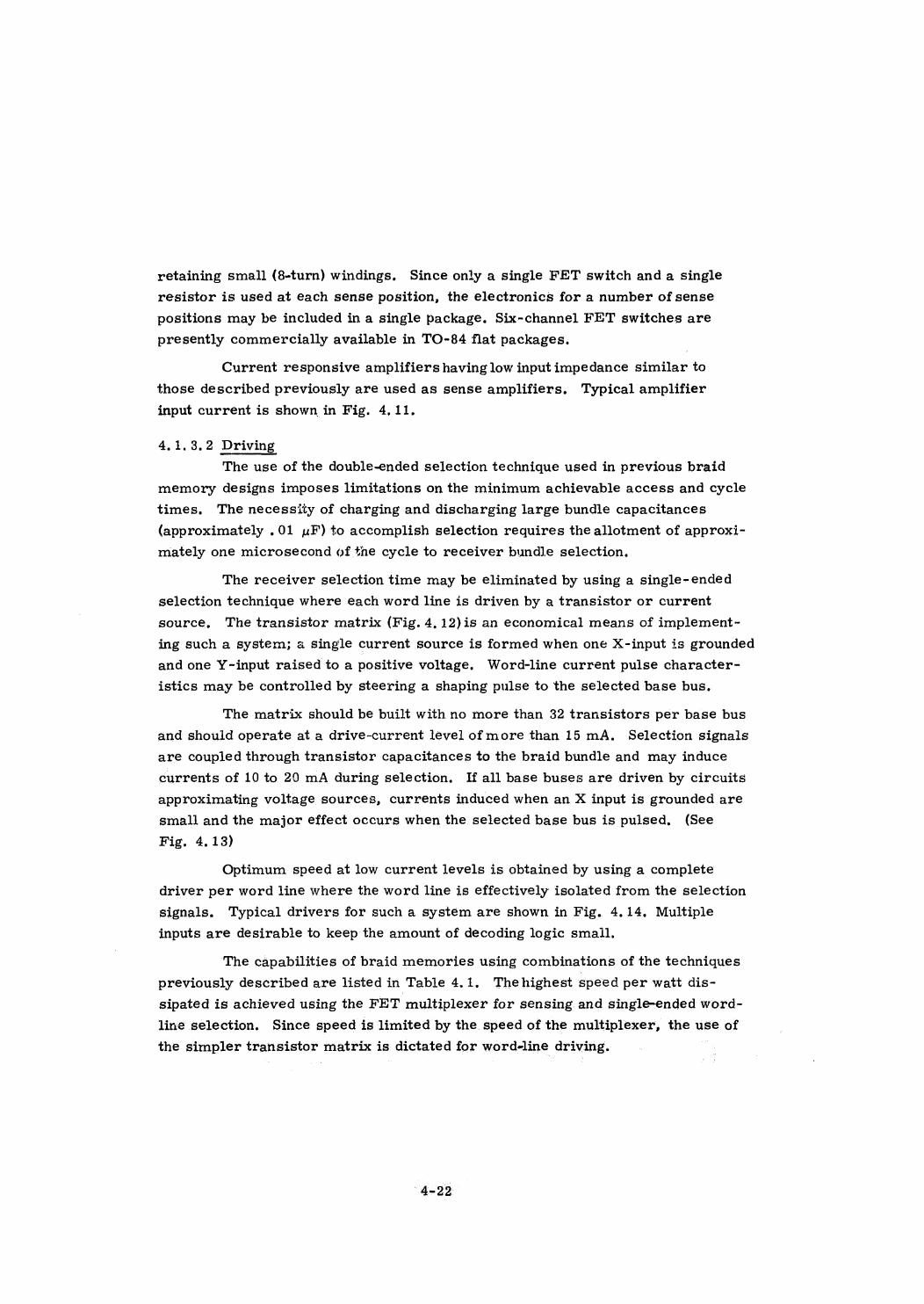
retaining small (8-turn) windings. Since only a single FET switch and a single
resistor is used at each sense position, the electronics for a numberof sense
positions may be included in a single package. Six-channel FET switches are
presently commercially available in TO-84 flat packages.
Current responsive amplifiers having low input impedance similar to
those described previously are used as sense amplifiers, Typical amplifier
input current is shown in Fig. 4,11.
4.1.3.2 Driving
The use of the double-ended selection technique used in previous braid
memory designs imposes limitations on the minimum achievable access and cycle
times. The necessity of charging and discharging large bundle capacitances
(approximately .01 uF) to accomplish selection requires the allotment of approxi-
mately one microsecond wf tne cycle to receiver bundle selection.
The receiver selection time may be eliminated by using a single-ended
selection technique where each wordline is driven by a transistor or current
source, The transistor matrix (Fig. 4,12)is an economical means of implement-
ing such a system; a single current source is formed when one X-input is grounded
and one Y-input raisedto a positive voltage. Word-line current pulse character-
istics may be controlled by steering a shaping pulse to the selected base bus.
The matrix should be built with no more than 32 transistors per base bus
and should operate at a drive-current level of more than 15 mA. Selection signals
are coupled through transistor capacitances to the braid bundle and may induce
currents of 10 to 20 mA during selection. If all base buses are driven by circuits
approximating voltage sources, currents induced when an X input is grounded are
small and the major effect occurs when the selected base bus is pulsed, (See
Fig. 4.13)
Optimum speed at low current levels is obtained by using a complete
driver per word line where the wordline is effectively isolated from the selection
signals. Typical drivers for such a system are shown in Fig. 4.14, Multiple
inputs are desirable to keep the amount of decoding logic smail.
The capabilities of braid memories using combinations of the techniques
previously described are listed in Table 4.1. Thehighest speed per watt dis-
sipated is achieved using the FET multiplexer for sensing and single-ended word-
line selection. Since speed is limited by the speed of the multiplexer, the use of
the simpler transistor matrix is dictated for word-line driving.
“4=22.
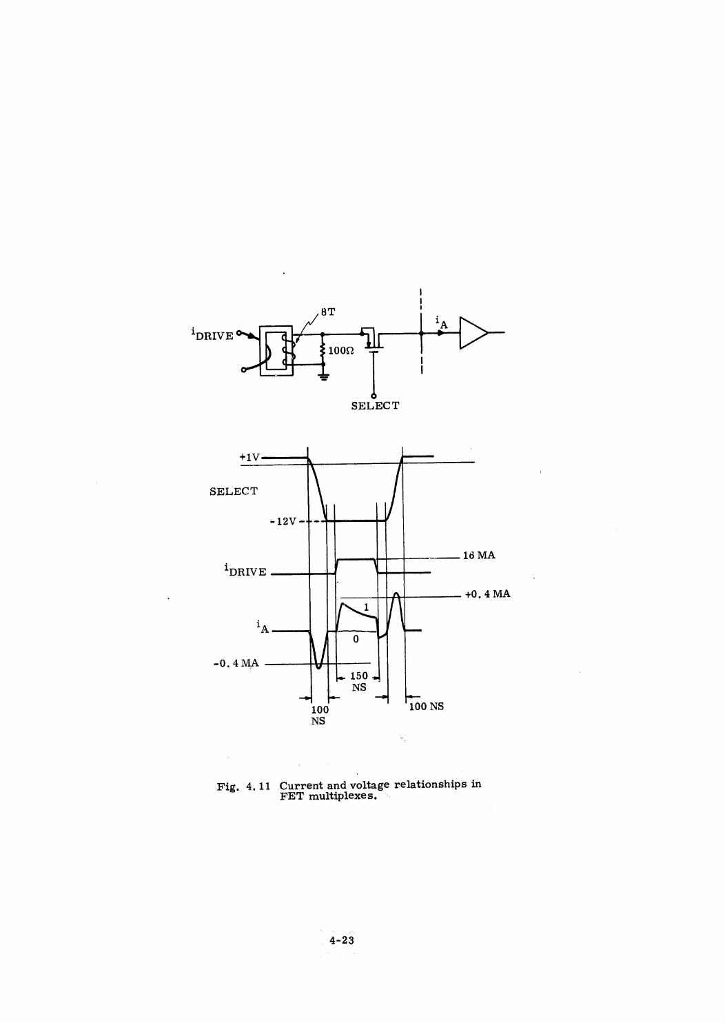
inRIVE Mal
on”
SELECT
+1V nme
SELECT
*12V-+-
16 MA
1DRIVE
A +0.4MA
/
LA0
-0,4MA Y _.150
_ NS—- — —m iam
100 100 NSNS
Fig. 4.11 Current and voltage relationships inFET multiplexes.
. 4-23
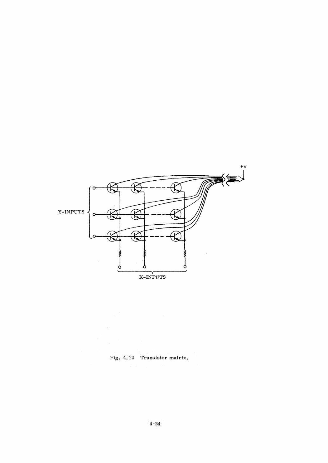
Y-INPUTS <
I 2+V
[|
b (Ss
$ $> j
) a)\ Y /
X-INPUTS
Fig, 4.12 Transistor matrix.
4-24
a
“R
O-——
;Vy
é
t+ * SELECTED UNSELECTED
Vy emineenensases
Ib
ip . ;
rom
Zi —/ \_ Fig. 4. 13 Parasitic currents due to transistor capacitances.
4-25
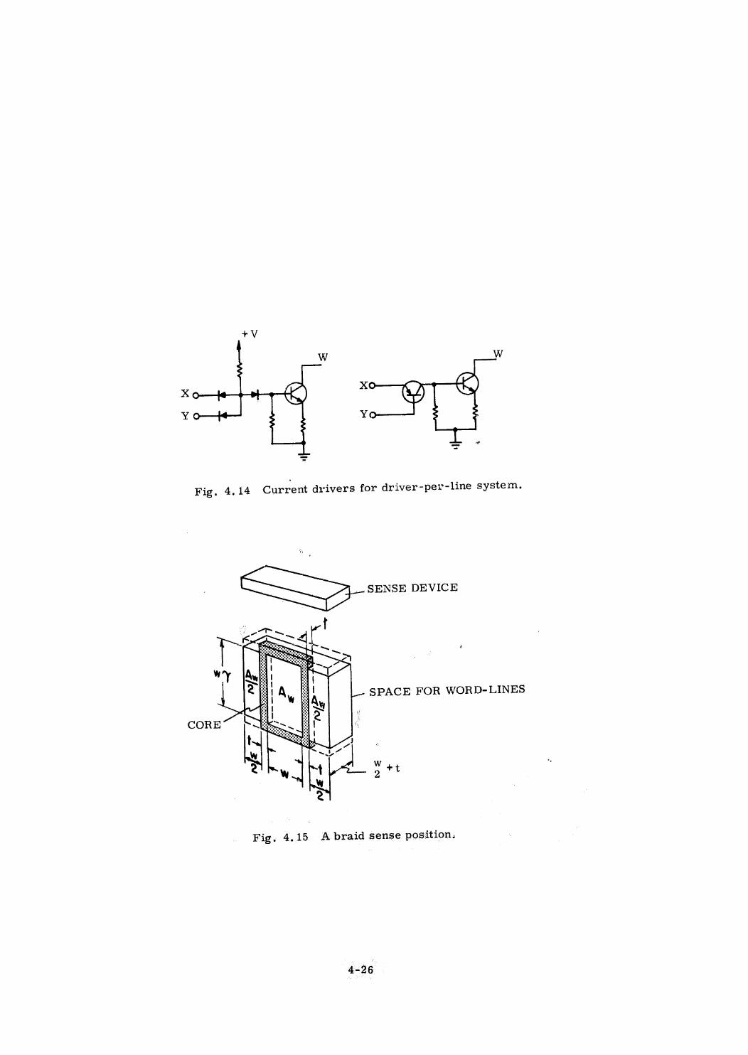
+V
Ww
.
¥
Current drivers for driver-per-line system.
AAA
Fig. 4.14
SENSE DEVICE
SPACE FOR WORD-LINES
CORE
S~ ~~,
Mtwe
Fig. 4.15 A braid sense position.
4-26
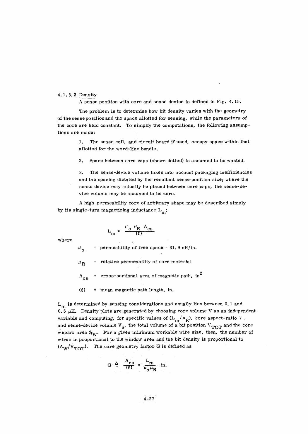
4,1.3.3 Density
A sense position with core andsense device is defined in Fig. 4.15.
The problem is to determine how bit density varies with the geometry
of the sense position and the space allotted for sensing, while the parameters of
the core are held constant. To simplify the computations, the following assump-
tions are made:
1. The sense coil, and circuit board if used, occupy space within that
allotted for the word-line bundle.
2. Space between core caps (shown dotted) is assumed to be wasted.
3. The sense-device volume takes into account packaging inefficiencies
and the spacing dictated by the resultant sense-position size; where the
sense device may actually be placed between core caps, the sense-de-
vice volume may be assumedto be zero,
A high-permeability core of arbitrary shape may be described simply
by its single-turn magnetizing inductance Ly
MB uM, AL = oe _R “csm (£)
where ,
H. = permeability of free space = 31.9 nH/in.
KR = relative permeability of core material
Acs = cross-sectional area of magnetic path, in”
(£) = mean magnetic path length, in.
Lin is determined by sensing considerations and usually lies between 0.1 and
0.5 wH. Density plots are generated by choosing core volume V as an independent
variable and computing, for specific values of (L,./ Up), core aspect-ratio Y ,
and sense-device volume Vg: the total volume of a bit position Vror and the core
window area Any For agiven minimum workable wire size, then, the number of
wires is proportional to the window area and the bit. density is proportional to
(Ay/Viror): The core geometry factor G is defined as
GA cs 2m |
4-27
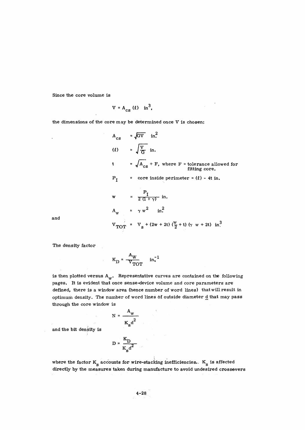
Since the core volume is
- . 3V =A,(2) in’,
the dimensions of the core may be determined once V is chosen:
Acs = Jav in?
(Q) = Ps in,
t = JA + F, where F = tolerance allowed forcs "has
fitting core,
Py = core inside perimeter = (@) - 4t in.
= P,
WwW = Za+y)~ in.
7 2 . 2Ay F yw in.
and' | Ww - 3Vror V5 + (2w + 2t) (x + t) (y w + 2t) in‘
The density factor
Ky = yw in)!TOT
is then plotted versus Ay. Representative curves are contained on the following
pages. It is evident that once sense-device volume and core parameters are
defined, there is a windowarea (hence number of word lines) thatwillresult in
optimumdensity. The number of word lines of outside diameter d that may pass
through the core window is
AN= —
| | Kaandthe bit density is
D= =DKd
wherethe factor K, accounts for wire-stacking inefficiencies.. K, is affected
directly by the measurestaken during manufacture to avoid undesired crossevers
4-28
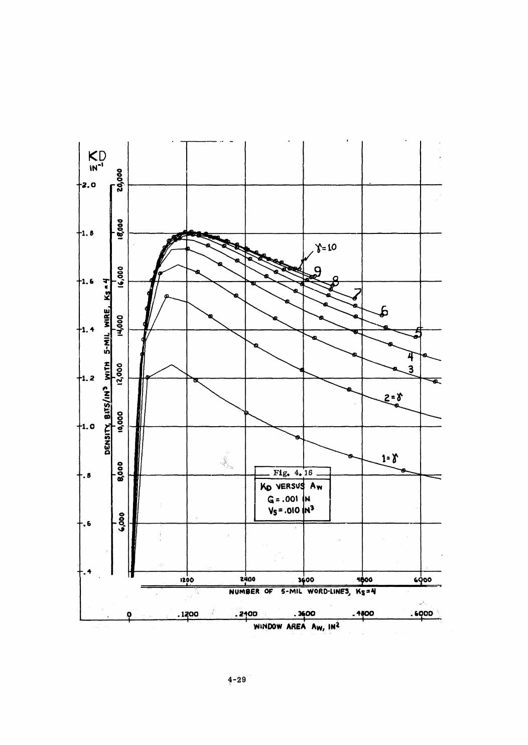
IN" ogoe
Q ;+r2,.0 rs
Ss
Ss71.8 P oS
°oeoSo
7T1.6 Ty
Zi |
wi]
Ff:
y** az ts =F
in
z: po
a8 3+t1.2 StS
—<—
‘ Se
3 2=t
zl 3 MN a
T1.0 rire3 Sel
ui
oe
° sf1=X
3 Fig. 4.16 |7-8 ro ; ge ~, tn,
' Kp VERSUS AwG=.001 IN
4+ ¢ ~§
“it
+.4 —1200 2ugo 3600 4 goo
: NUMBER OF 5-MIL WORD-LINES, Ks=4 :
9 _slz00 | -2400. 600 4800 6900"WINDOW AREA Aw, IN@-
4-29
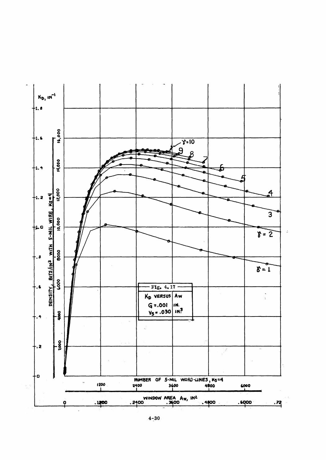
4-30
* aah
Kp, in”
4i.e
°
3Pp es Y=10
—Reee-tde OQ
poe F° E,- ——4 é
8 f_-° ' Cyet fz y ee >
° Af fo
tie TS if Po. Pa et. uf w "
el f 37
Ro ars ~_ eoi | t= 2zr
$$
5 3+3 s -S a
m
‘
~ =2a °o
oS
+.6 rTs Fig. 4. 17
Z| Kp VERSUS| Aw
a G =.00! In. .
++ fs
°Q-l
Pez FS th
bo | _RUMBER OF 5-MIL WORD-UINES, Ks=4
rae 2400 3600 4600 000
WINDOW AREA Aw, iN@ -. 1200 - 2400 . 3600 ° vw $800 - 6000 »
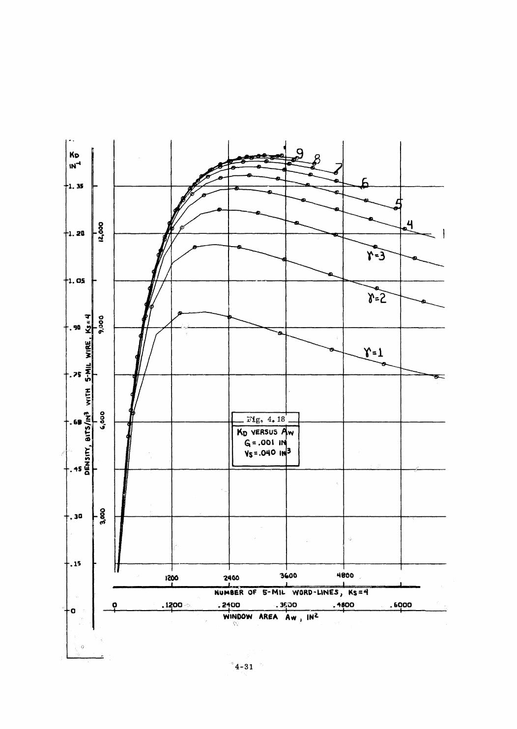
Kp
int |
41.35 + eeSe, 6
laf yo a ee
+1.05
4. T
« wDoo
J9,900
N <—
1
N wm
DENSITY,
BITS
/IN?
~wiTH
5S-MIL
WIRE,Ks=4
°
+. 69S 3 Tig, 4,18w)
Kp VERSUS Aw
G=.001 |Vs=.040 in?
+. 48 r -
a
T. 15 bes |
1200 2400. 36006 4600 |
a Lenm, i | 1NUMBER OF 5S- MIL WORD-LINES , Ks=4
° .1200- . 2400 3600 . 4800 __.6900 “FO " —T 7
| WINDOW AREA Aw , IN¢ g
“4-31
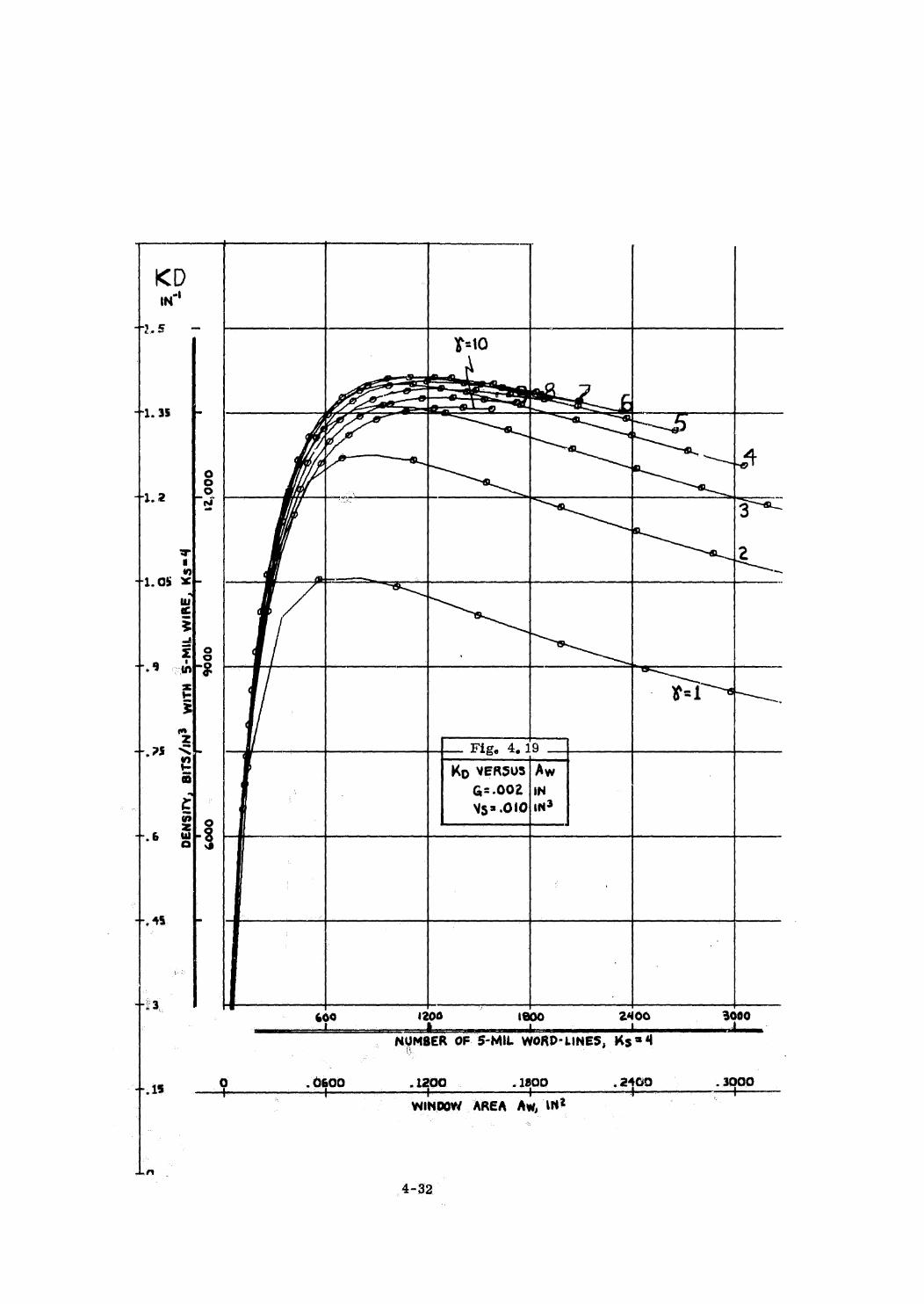
in”
+T1.2 -
$=10
CA J
eee)
+1.35 f peih
6 LAo
4 A1.2 we is
r (4
T1.05 <-
wi]«£>2z18
7.9 org
E
Ysaee
2TT. as S$ od Fig. 4, 19
e Kp VERSUS Awa G=.002 |in
Ec Vs 2.010] 1N?Lio .
T.6 a -3. wre
T, 45 bees
: 600 1200 1800 24006 3000__i 4 a i L t
NUMBER OF5-MIL WORD-LINES, Ks=4
+ 45 0 . 0600 -1200 - 1800 2400 - 3000
| WINDOW AREA Aw, IN?
la4-32
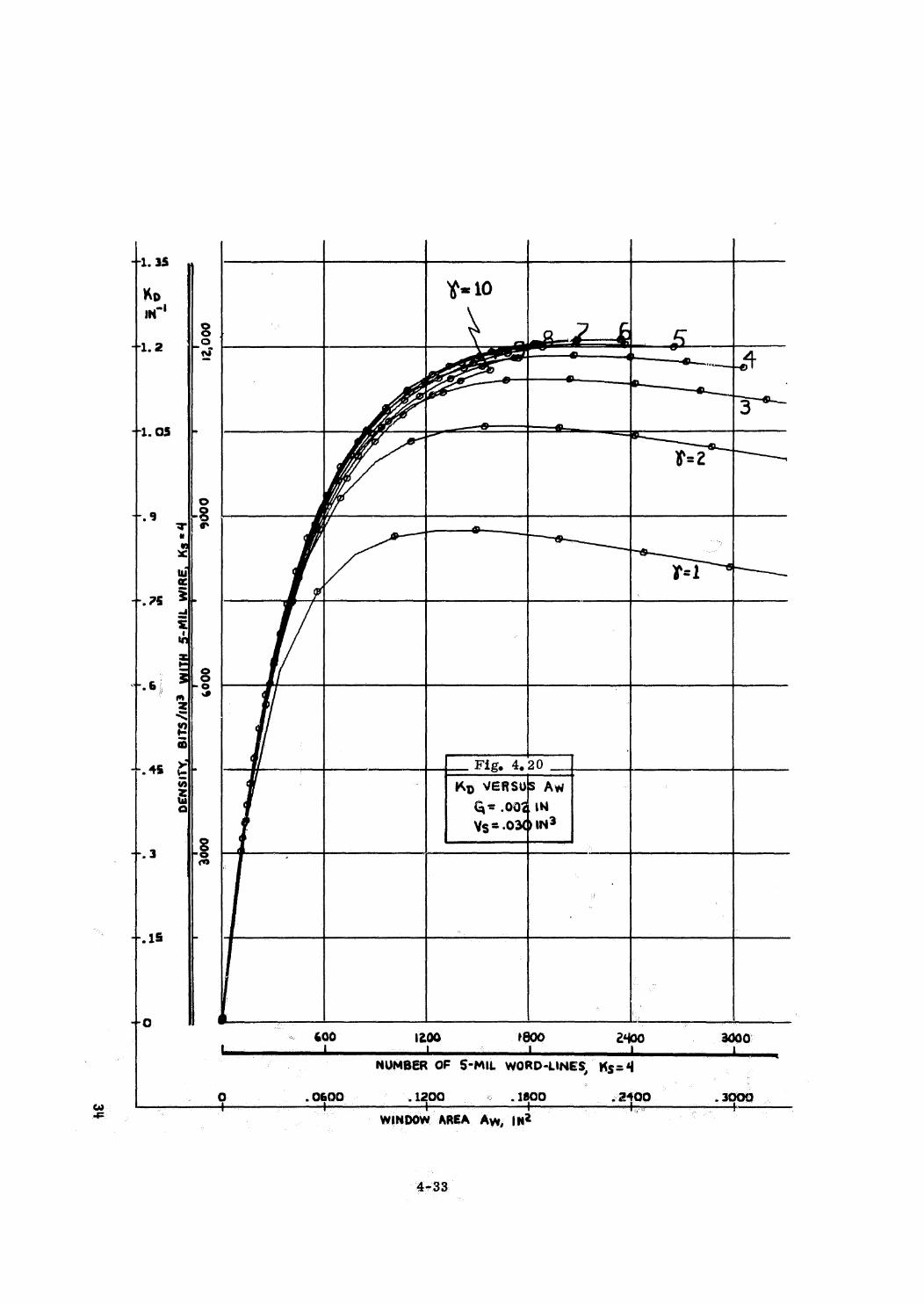
1L
he
r. 75
Ly | u®
12,000
[ ny
Let
r1. OS
9000
¢000
+6)“ @
z~
e©
Las 2 Hig. 4,20z Kp VERSUS Aw
a G= .004 INVs=.0 in3
r.3 3
rO So .Xs 600 1200 "600 2400 3000:. 1
NUMBER OF S-MIL WORD-LINES, Ks=4 a
.0600 —_—-. 1200 < 100.400 . 3900
- WINDOW AREA Aw, IN@
4-33
A.
Hi. 35
+t1.2
r1. OS
4_5-Mib
¥=103 fs[2 -
rt
4 aa PR
z
46 xtcl S3
mo2
>E .7.45 or . Fig. 4.21
~ Ko VERSUS) Aw
al G=.002 1& Visg2.040 PN?a
+.3
+.15
°
+9 , a.
600 1200 1g00 . 2400 3000= i... i 4 ee t a
NUMBER OF 5-MIL WORD-LINES, Ks=4
O° .0600 «1200S.1800 . 2400, -.3900 -
7
WINDOW AREA Aw, IN?
4,2
within the word-line bundle; the density scales on the curves shown assume a
stacking factor of 4. Forwire sizes of AWG38 to 42, optimum density is
achieved when 500 to 2000 word lines are used. The length of the word-line
bundle must be limited to prevent excessive signal degradation, and a braid
of more than 512 cores is presently felt to be impractical. Since the capacity
of a high-density braid is thus set at 0.25 to 1, 0-million bits, a larger storage
capacity is best obtained by using a numberof 0.5 to 1, 0«million-bit modules,
It is to be stressed that the density figures obtained by the preceding
sense-position analysis must be reduced by a factor of threeto five to obtain
realistic density figures for a complete braid memory. A major goal of final
packaging is to reduce the volume consumedby driving/decoding electronics,
bundle potting, and necessary hardware, Densities of 6000 to 12,000 bits per
cubic inch are attainable if the volume consumed by peripheral hardware is kept.
within a factor of two or three of the volumeof the information field.
Plated«Wire Memory
As noted earlier, the advanced computer requires increased speed, capacity,
and flexibility of erasable memories. In view of these requirements, a study was
_ initiated to determine the suitability of Permalloy plated wire for a main erasable
and/or scratchpad memory subsystem. The MIT study has pursuedthree major
lines of inquiry:
Exploratory production of plated wire to determine optimal fabrication
and quality control techniques. ,
Memory-stack mechanical design for high density, good electrical
performance and tolerance for the spaceborne environment.
Memory eiectronics development suitable for microminiaturization
and incorporation with the memory stack into a unified assembly.
4,2,1 Wire Production
4.2.1.1 Review of Wire Development at MIT
4, 2.1.1.1 Purpose of Wire Development
Advanced memory systems for aerospace applications must take advan-
tage of improvements in electronic circuitry and packaging techniques now under
development.
4-35
A memoryof this type should employ a highly reliable scheme of nondestructive
readout and be electrically alterable. Improvements in the following areas are
needed;
Weight and volume reduction
Cost
Reliability
Reduced Power Consumption
The prime requisite in a memory system in this application is high reliability
under the environmental conditions which it will meet in space applications.
Magnetic films hold great promise in being able to fulfill the require-
ments of the next generation of aerospace memories. The plated-wire memory
in particular appears to be the most attractive as a result of its high output
comparedto planar thin-film memories,along with high speed and simplicity.
Basically, the device (shown in Fig. 4.22) consists of 5-mil Be-Cu wire
plated with an 81% Ni-19% Fe layer of Permalloy about 10, 000-angstroms thick
crossed orthogonally by word lines. The distinguishing feature of the plated-
wire device is that the easy axis is oriented along the circumference of thewire
in a closed-flux configuration. The resultant low demagnetization value in the
remanent state permits relatively thick films to be used. Since the amplitude
of the output is directly proportional to the volume of the material and thus to ° .
the thickness of the element, a relatively thick-plated wire device is capable of
outputs of 15 to 50 millivolts in the destructive mode and on the order of 3to .
10 millivolts in the nondestructive mode,
The operation of a plated-wire device is similar to the operation of a
single flat film in many respects. As in a flat film, the application of a word
current I causes the magnetization vector to rotate toward thehard direction
with the polarity of the output signal identifying the stored bit, and the central
copper wire serving as the sense line. The closed-flux configuration of the
platedawire device enables its magnetization to be rotated to an angle smaller
than 90 degrees. Upon termination of the read current, the magnetization re-
turns to the original state. This represents a nondestructive readout (NDRO).
Writing is accomplished by driving a small write current, Ia of the
- appropriate polarity through the copper wire prior to terminating the ''Read”
current, in a manner identical to the steering of flat films. Since the plated
wire is capable of both writing and reading speeds in the submicrosecond region,
it can be used with equal ease in scratchpad as well as in program-store appli-
cations..
4-36
TRANSVERSE DRIVE SOLENOID
MAGNETIC FILM
CENTRAL CONDUCTOR
Fig. 4.22 Basic film device, |
A3T
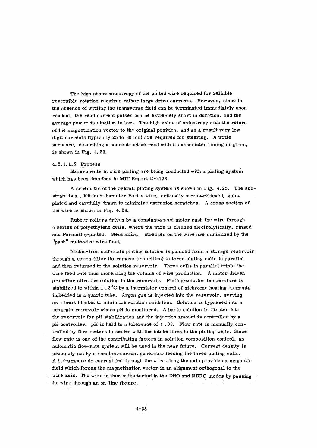
The high shape anisotropy of the plated wire required for reliablereversible rotation requires rather large drive currents. However, since in
the absence of writing the transverse field can be terminated immediately upon
readout, the read current pulses can be extremely short in duration, and the
average power dissipation is low. The high value of anisotropy aids the return
of the magnetization vector to the original position, and as a result very low
digit currents (typically 25 to 30 ma) are required for steering. A write
sequence, describing a nondestructive read with its associated timing diagram,
is shown in Fig. 4. 23.
4,2.1.1.2 Process
Experiments in wire plating are being conducted with a plating system
which has been decribed in MIT Report E-2128,
A schematic of the overall plating system is shown in Fig. 4.25. The sub-
strate is a .005-inch-diameter Be-Cu wire, critically stress-relieved, gold=
plated and carefully drawn to minimize extrusion scratches, A cross section of
the wire is shown in Fig, 4, 24.
Rubber rollers driven by a constant-speed motor push the wire through
a series of polyethylene cells, where the wire is cleaned electrolytically, rinsed
and Permalloy-plated. Mechanical stresses on the wire are minimized by the
"push" method of wire feed.
Nickel-iron sulfamate plating solution is pumpedfrom a storage reservoir
through a cotton filter (to remove impurities) to three plating cells in parallel
and then returned to the solution reservoir, Three cells in parallel triple the
wire feed rate thus increasing the volume of wire production. A motor-driven
propeller stirs the solution in the reservoir. Plating-solution temperature is
stabilized to within + ,2°C by a thermistor control of nichrome heating elements
imbedded in a quartz tube. Argon gas is injected into the reservoir, serving
as a inert blanket to minimize solutien oxidation. Solution is bypassed into a
separate reservoir where pH is monitored. A basic solution is titrated into
the reservoir for pH stabilization and the injection amount is controlledby a
pH controller. pH is held to a toleranceof + .03,. Flow. rate is manually con-
trolled by flow meters in series with the intakelinesto the plating cells. Since
flow rate is one of the contributing factors in solution composition control, an
automatic flow-rate system will be used in the near future. Current density is
precisely set by a constant-current generator feeding the three plating ceils.
A 1, O-ampere dc current fed throughthe wire along the axis provides a magnetic
- field which forces the magnetization vector in an alignment orthogonal to the
, wire axis. The wire isthen pulgetested in the DRO and NDRO modes by passing
the wire through an on-line fixture. | | -
4-38
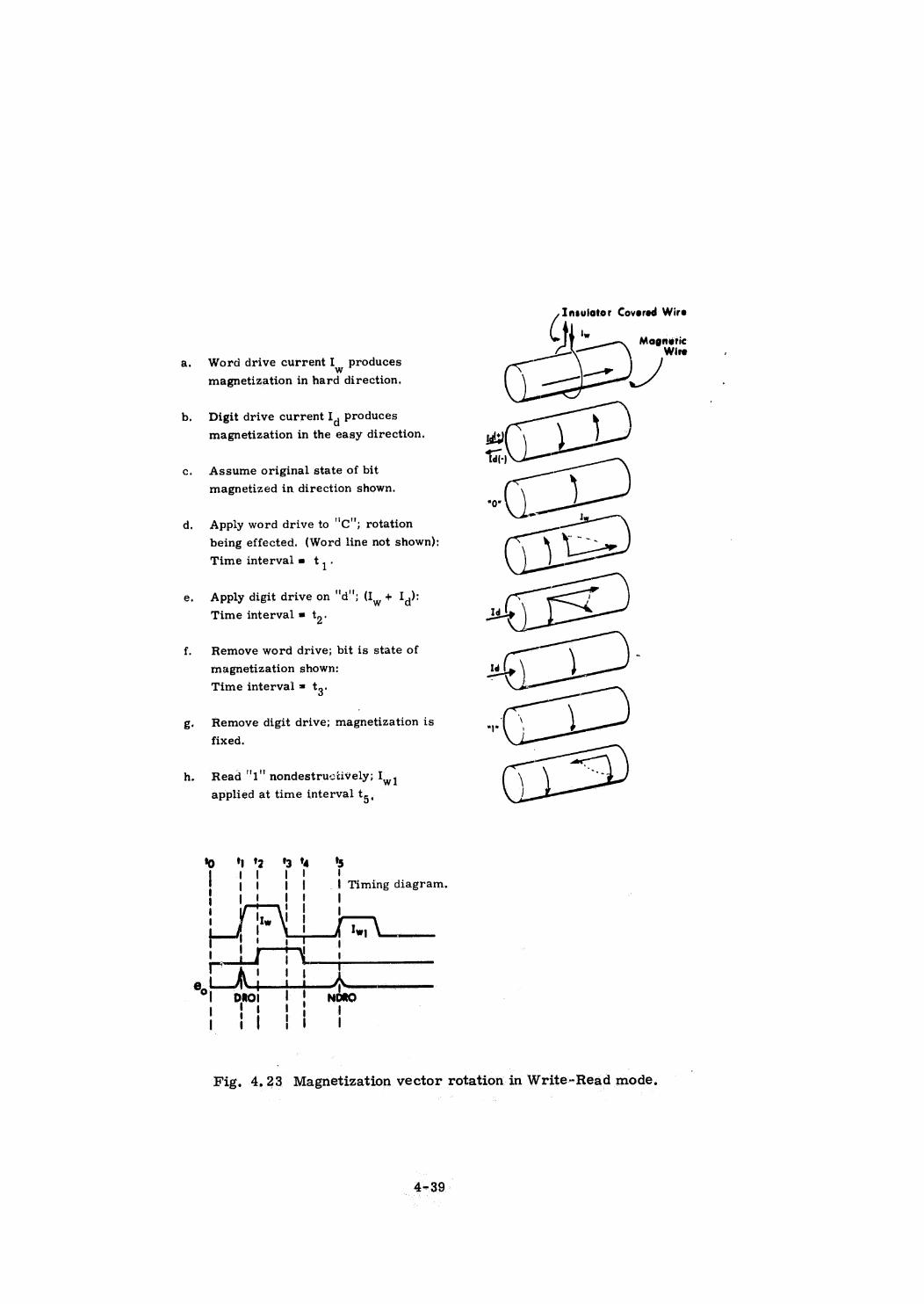
Word drive current I produces
magnetization in hard direction.
Digit drive current Id produces
magnetization in the easy direction.
Assumeoriginal state of bit
magnetized in direction shown.
Apply word drive to ''C"'; rotation
being effected. (Word line not shown):
Time interval = t 1°
Apply digit drive on "d"; (I, + Ig):
Time interval = to.
Remove worddrive; bit is state of
magnetization shown:
Time interval = t,-
Remove digit drive; magnetization is
fixed.
Read "1" nondestructively; I, ,
applied at time interval te,
| 9 ty 4 tg
j
_4 Timing diagram.||
Insulator Covered Wire
—CaeoDId(-)
Fig. 4.23 Magnetization vector rotation in Write~-Read mode.
4-39.
:
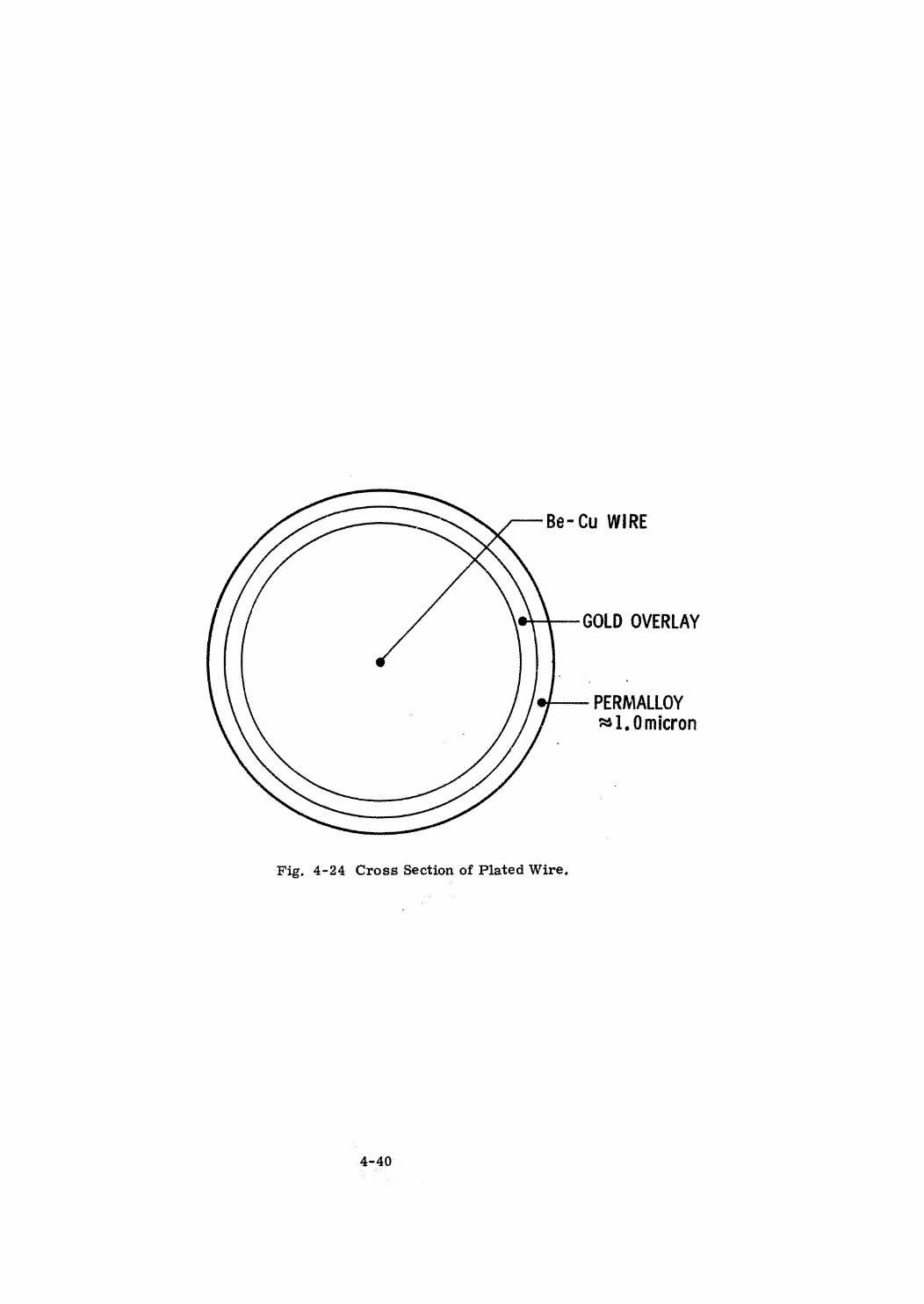
-Be-~Cu WIRE
GOLD OVERLAY
PERMALLOY~1.,0micron
Fig. 4-24 Cross Section of Plated Wire.
4-40
ALIGNMENT " FIELO
CURRENT
et
CONSTANT CONSTANT Pulse
eee CURRENT CURRENT cracuitssuery SOURCE source
= |mm O. :
CLEANING PLATE HO RINSE PLATE oe MONITOR
man) CONSTANT ‘ ; =BE-CU WIRE EO KALINE - ~coer patna nC PERMALLOY 4 conmact DRO, NORO
Daive RINSE COPPER, ETC , SIGNAL
Fig. 4.25 Present plating system.
4.2.1.2 Experimental Resuits with Existing System
4,2,1.2.1 Use of a Spectrophotometer "on-line" for Detecting Plating
Solution-Composition Changes
Initial experiments with a spectrophotometer revealed a rapid
reduction of Fe in the plating solution (0.1%/hr). To minimize this oxidation
loss an inert gas wasbubbledinto the plating solution reservoir, Measure-
ments indicated a reduction of Fe of 0,002% Fe/hr after inert-gas injection.
This was a decided improvement. Figure 4.26 is a plot of % Fe as a function
of Elapsed running time" in hours. Plating solution was sampled at specific
time intervals and Fe content was then measured at the MIT Metallurgy Dept,
Percent transmittance as a function of ''Elapsed running time" in hours is shown
in Fig. 4.27.
A final plot of % Fe as a function of percent transmittance (in Fig. 4.28)
resulted from the correlation of the previous two curves. The final curve is
very useful for detecting on-line "solution'' composition changes as function of
transmittance. Asensitivity cf 0.1% Fe/10% T is revealed from this plot.
0.01% changes in Fe content should therefore be detectable with this device.
The spectrophotometer was then incorporated into a control system for
automatically controlling Fe content within predetermined set limits. This sys-
tem will be in operation soon as a control device. The system should stabilize
Fe content over long periods of running time (possibly hundreds of hours).
4,2,1.2.2° Use of a Spectrophotometer to Detect Composition Changes in
Plated Wires
Feasibility of using a spectrophotometer with a reflectence attachment
to measure composition of plated wires was investigated. A number of wire
samples of known composition (average composition in a length of wire approx-
imately four inches in length) were sent to Bausch & Lomb to determine reflectance
of various wires as a function of composition.
Results revealeda change of 0.1% Fe/1.0% Ras shown in Fig. 4.29.
Measurement sensitivity is adequate but repeatability has not been determined
by Bausch & Lomb to date. The method is promising, however, and will be
further investigated.
4.2.1. 2, 3 Wire Substrate Studies
A randomly oriented crystal structure is desirable as a prepilate prior to
plating Permalloy. Anisotropy is randomized because of this, and magnetic
vector skew and dispersion is minimized, .
4-42
£b->
%Fe
(sol
utio
n)
1,54
2.0
1,0
0.5
1 j 1 | 1 i 1 J
40 60 80 100 120 140 160 . 180
ELAPSED TIME (HOURS)
Fig. 4.26 Time variation of Fe percentage.
vv-F
%Transmittance
100
80
20 © 40 60 80 100 120
ELAPSED TIME (HOURS)
Fig. 4.27 Transmittance variation.
‘A j.W °
a I ! I I I L L |140 160 186
% Transmittance
70
60
50
4030
2010
0.5
1.0
%Fe
insolution
Fig.
4.28
Spectrophotometer
calibrationplot.
4~45
bo =wo
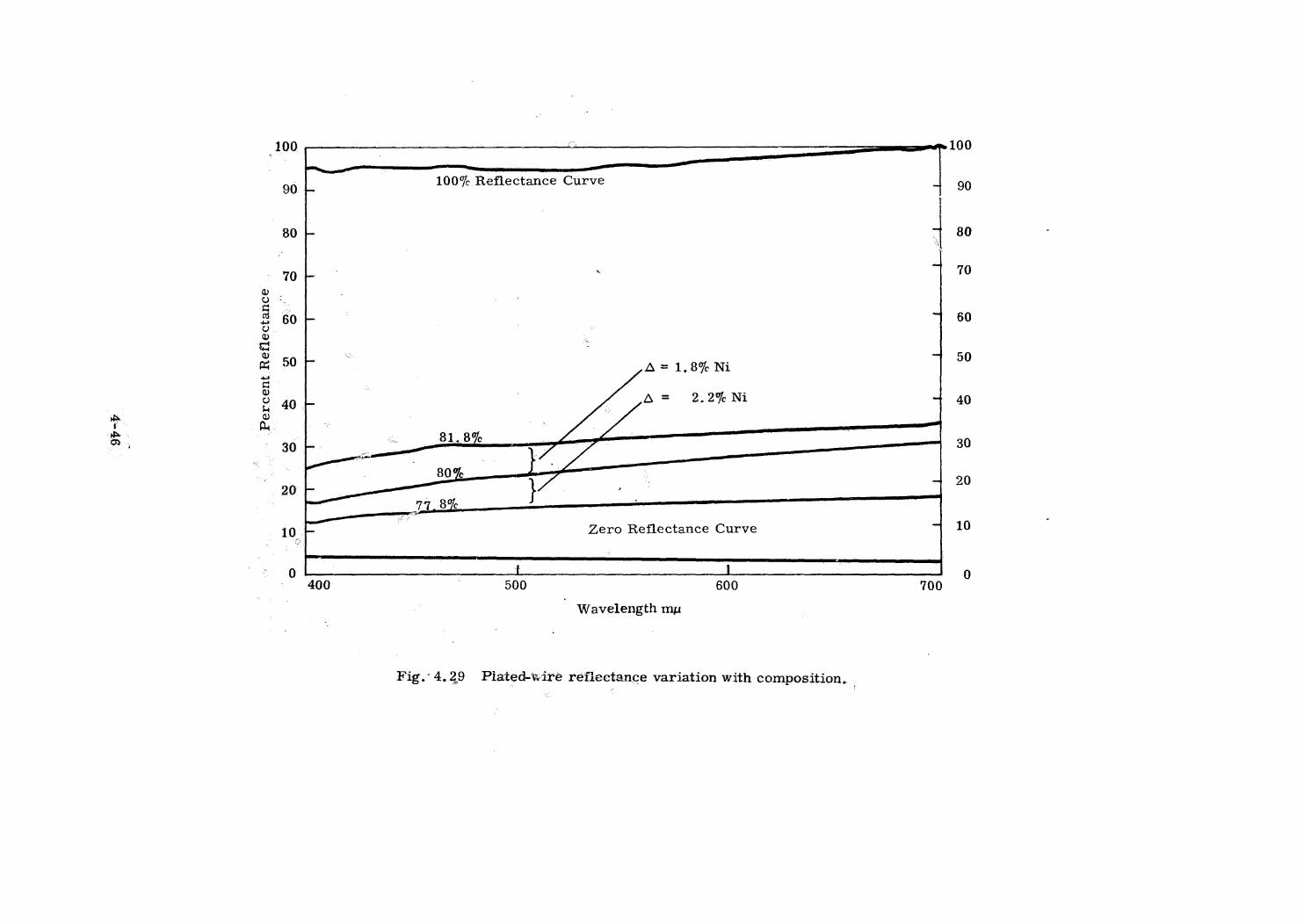
9b-F
Percent
Reflectance
100 : : it anemone 1() (0)
90 L 100% Reflectance Curve | 90
80 + + 80
70 - . “| 70
so + 60
. 4 5050 = 1,8% Ni
40 = 2.2% Ni + 40
30 To a30
sou 2020neLt 8%
if Zero Reflectance Curve 4 10
0 t 1 0
400 : 500 600 700
Wavelength mu
Fig..4.29 Piated-wire refiectance variation with composition. .
° A Nickel-rnaosphorous preplate has been experimented with and results
to date are preinising but not conclusive. On-line sense-voltage tests revealed
an improvement in sense-voltage uniformity with the preplate of approximately
50%, A reduction in easy-direction (Ho) coercive force also occurred (noted
by a reduction in digit current with word-current constant). He was compared
with a vendor's wire using a copper preplate, A 75% reduction in Ho was noted
with the Ni-P substrate. However, the digit-current disturb margin of the
vendor's wire was 5% wider. Copper preplates will also be studied by MIT in
the near future.
4,2,1.2.4 Pulse Measurements of Plated Wires
A fixture was designed to partially evaluate a 'Plated-Through Hole"
memory plane. Three "word"lines were cut from the memory plane, lined-up
adjacent to one another and insulated. This geometry simulated three word coils
in three separate planes as shown in Fig. 4.30. Center-to-center coil spacing
is 36.3 mils. This is not an exact simulation, however, in that ground planes
between coils were not included. The newer design will include ground planes
for shielding purposes. A program was set up to determine the effect of
adjacent word disturbing. The program is shown in Fig. 4.31. Table\4-2
shows the percentage change in voltage output with increasing adjacent-word
current. IfIpo = Ipga drastic change in output occurs as evidenced by the
table. The bit, however, retains its stored information. Coincidence df
Ino and Ing is a logical case that would not occur in actual memory operation,
however, ,
A more realistic evaluation of "adjacent-word line" disturbing has
word-current pulse Ing occurring after Ing and not in coincidence with it.
' The pulse-test fixture, converted as shown in Fig. 4.32, is also used
on- andoff-line for detection of sense-amplitude changes, On-line it is used in
conjuction with a series of gnse amplfiers and discriminators. Its function is
to detect changes in sense voltage and to feed back the change either to current
generators supplyingcurrent between the plating anodes and the wire or to a
titrator supplying eitheriron or nickel sulfamate tojthe plating solution reser-
voir, thus stabilizing wire composition (assuming of course that other para- .
meters are held constant). The former method is not feasible with the present
setup mainly because the drive-sense coils must be incorporated into the plating
cell, At present they are six inches from the cell, Tne latter method can be
used with the present setup and will be compared with the spectrophotometer
method of controlling wire composition. a
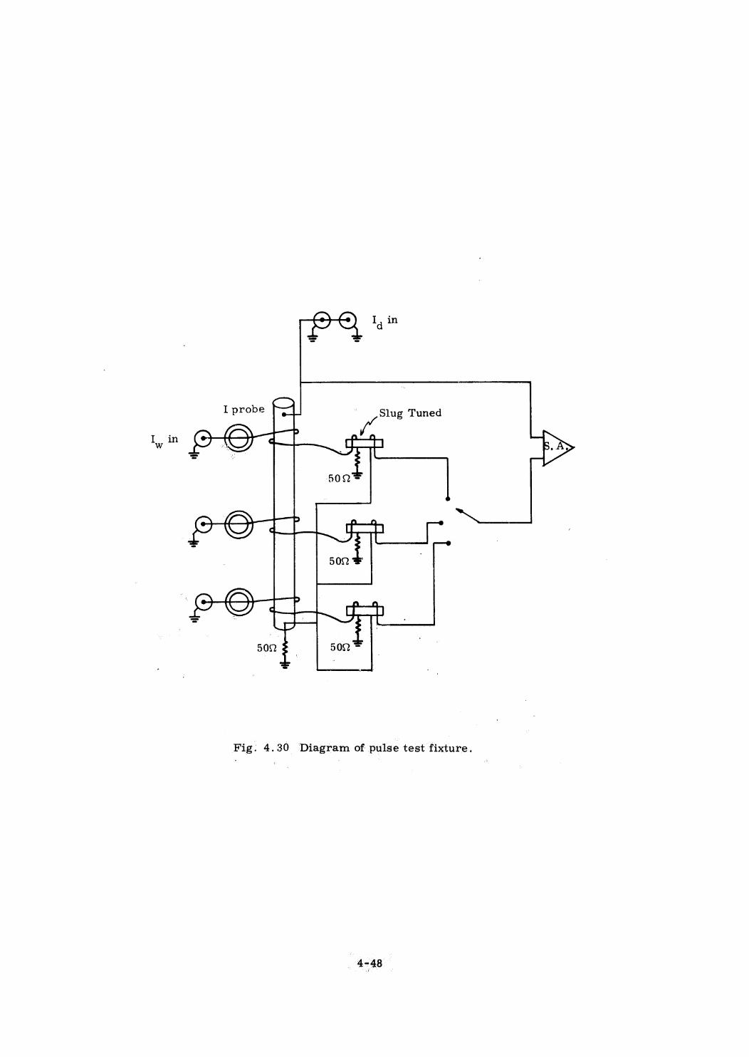
Pra I, in
I probe ‘Slug Tuned
[\10
502 502 *
Fig. 4.30 Diagram ofpulse test fixture.
4-48©
Seti pe cr
sad .
q
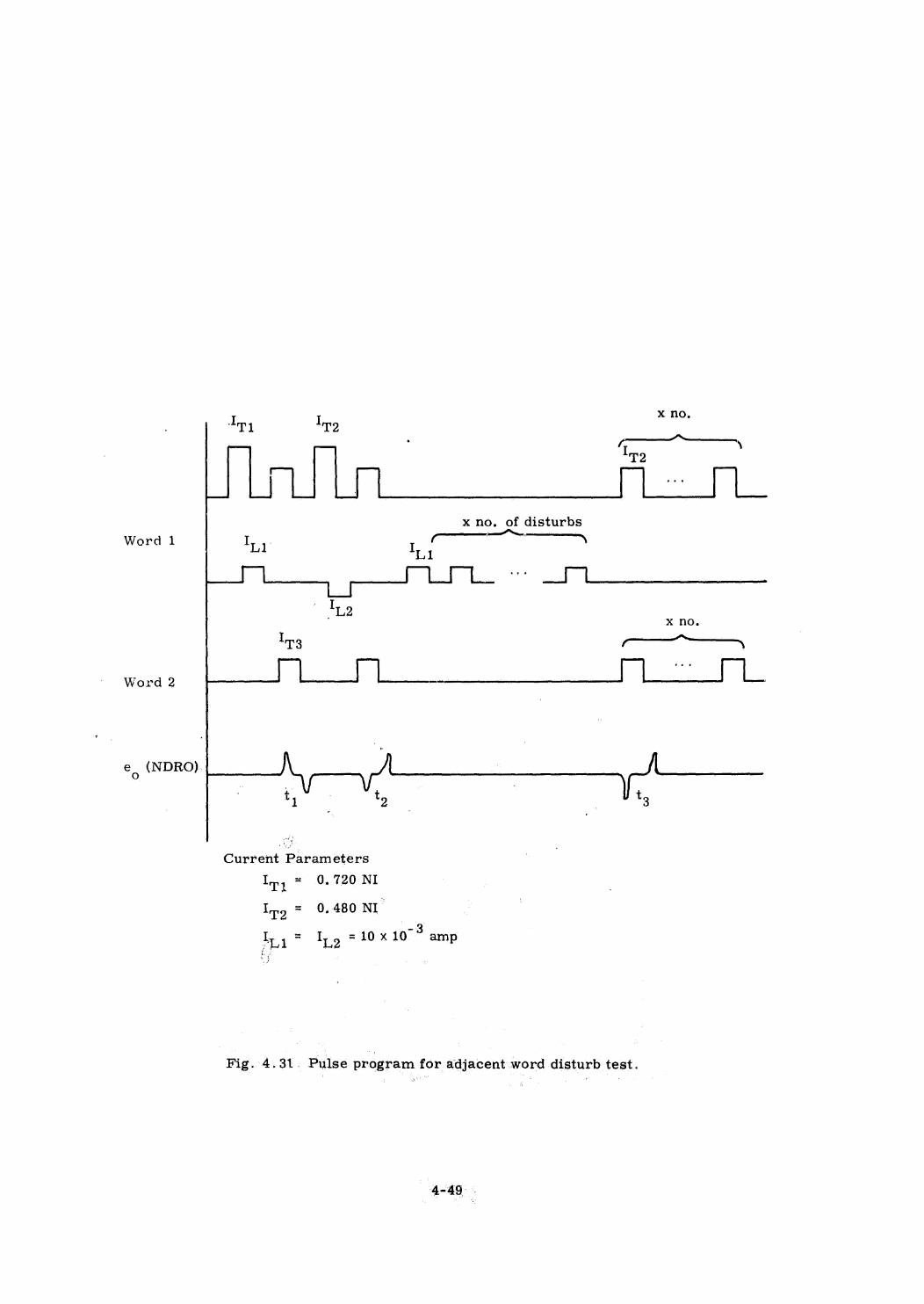
Iny Ing "eo
Ing
x no. of disturbs
Word 1 I, ,. C ~Ll Ty
mM MorMmLJte
x no.
Ing —_—
Word 2
ey (NDRO). NV 4/11 | 2
| | to Ets
Current Parameters
Tiny = 0.720 NI
Ing = 0,480 NI
. _ 4-3Ly = Lo = 10x10 ampytdef
Fig. 4.31. Pulse program for adjacent word disturb test.
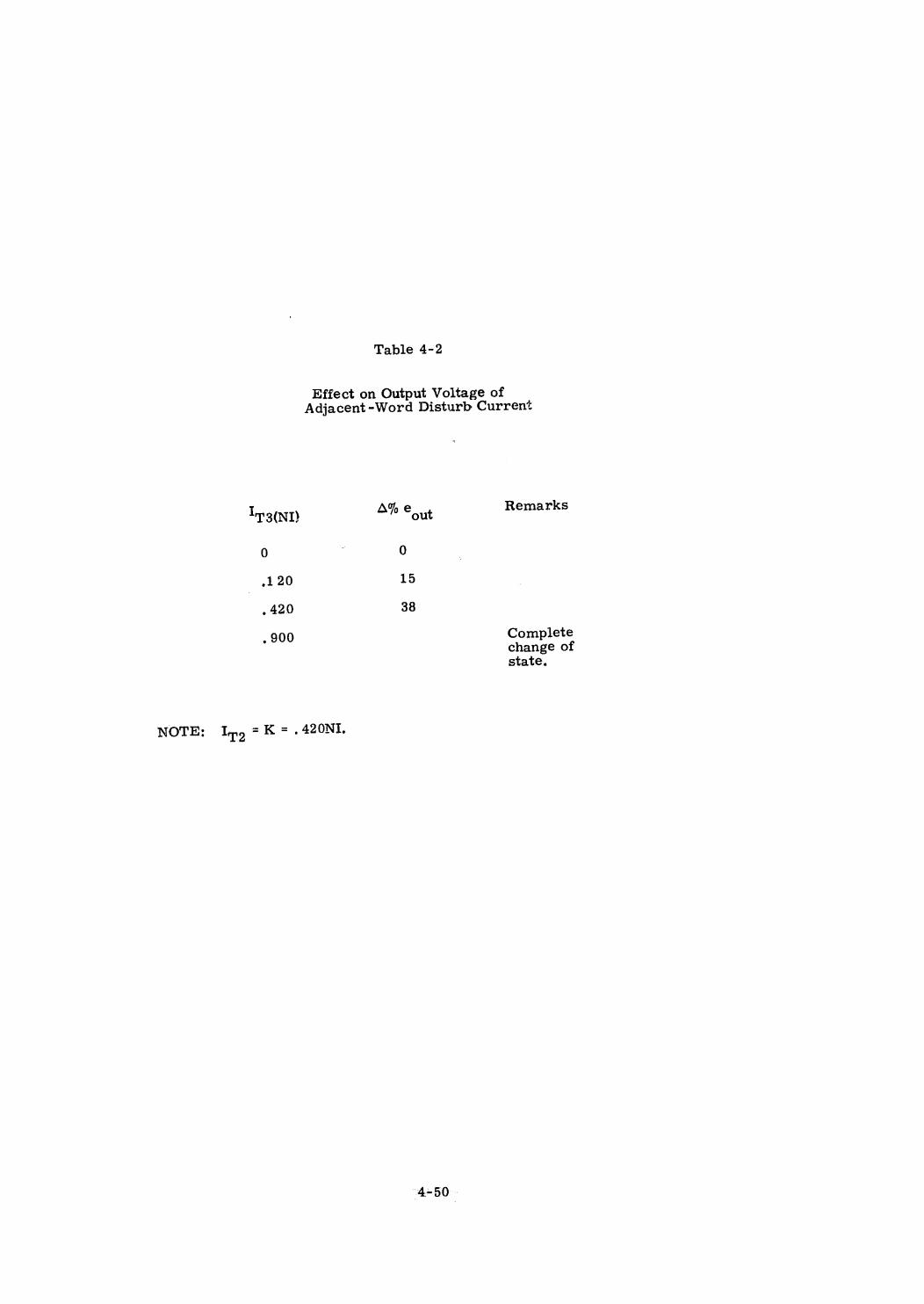
Table 4-2
Effect on Output Voltage ofAdjacent -Word Disturb Current
In3(N1)
0
.1 20
420
. 900
At eout
15
38
“4-50-
Remarks
Completechange ofstate.
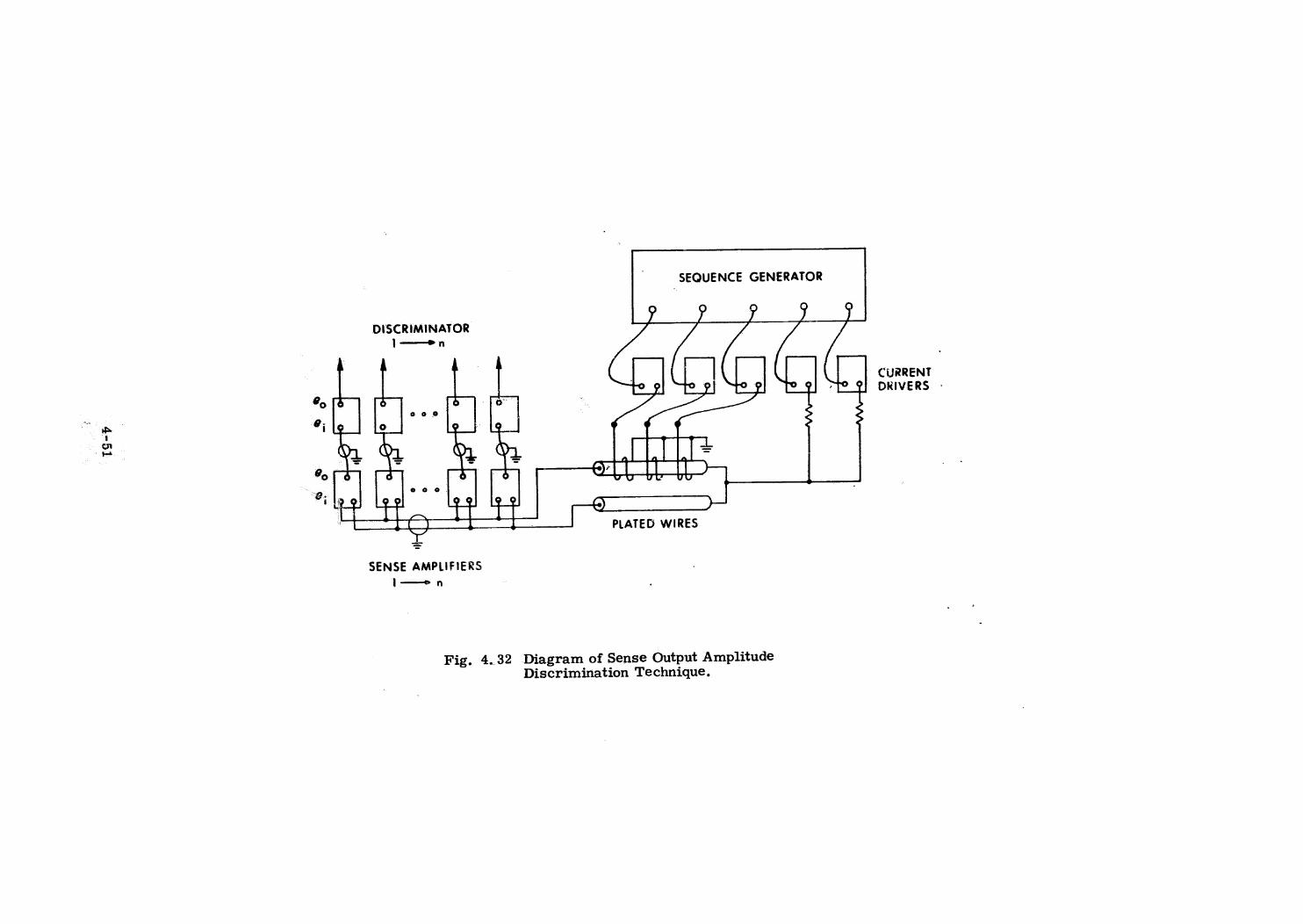
19>
8 [6 3° }
pp ip
SEQUENCE GENERATOR
2 ;
DISCRIMINATORi~-— en fo To 9
parenenmemrinenaes
que
oad
panne
I
3+— 3 eo 6
\
d \
oh Be
% TS 6 6 €) ras
=e. oo 0 j
ea Uy 4) le goTD PLATED WIRESYr
SENSE AMPLIFIERS
i-—r
Fig. 4.32 Diagram of Sense Output Amplitude
Discrimination Technique.
CURRENTDRIVERS -
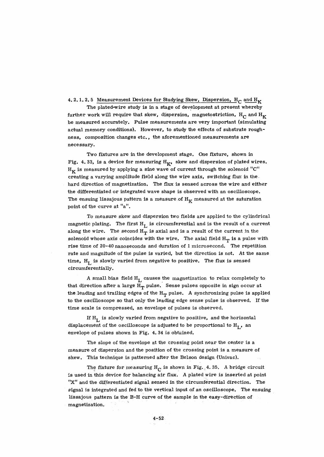
4,2.1.2.5 Measurement Devices for Studying Skew, Dispersion, Ho and Ay
The plated-wire study is in a stage of development at present whereby
further work will require that skew, dispersion, magnetostriction, Ho and Ay
be measured accurately, Pulse measurements are very important (simulating
actual memory conditions), However, to study the effects of substrate rough-
ness, composition changes etc., the aforementioned measurements are
necessary.
Two fixtures are in the development stage, One fixture, shown in
Fig. 4.33, is a device for measuring Ags skew and dispersion of plated wires.
H, is measured by applying a sine wave of current through the solenoid "C"'
creating a varying amplitude field along the wire axis, switching flux in the.
- hard direction of magnetization. The flux is sensed across the wire and either
the differentiated or integrated wave shape is observed with an oscilloscope,
The ensuing lissajous pattern is a measure of Hy measured at the saturation
point of the curve at "a",
To measure skew and dispersion two fields are applied to the cylindrical
magnetic plating. The first Ay is circumferential and is the result ofa current
along the wire, The second Hp is axial and is a result of the current in the
solenoid whose axis coincides with the wire, The axial field Hp is a pulse with
rise time of 20-40 nanoseconds and duration of 1 microsecond. The repetition
rate and magnitude of the pulse is varied, but the direction is not. At the same
time, Hy is slowly varied from negative to positive. The flux is sensed
circumferentially.
A small bias field H, causes the magnetization to relax completely to
that direction after a large Hyp pulse. Sense pulses opposite in sign occur at
theleading and trailing edges of the Hm pulse, A synchronizing pulse is applied
to the oscilloscope so that only the leading edge sense pulse is observed, If the
time scale is compressed, an envelope of pulses is observed.
If Ay is slowly varied from negative to positive, and the horizontal
displacement of the oscilloscope is adjusted to be proportional to Hy» an
envelope of pulses shown in Fig. 4. 34 is obtained.
The slope of the envelope at the crossing point near the center is a
measure of dispersion and the position of the crossing point is a measure of
skew. This technique is patterned after the Belson design (Univac).
The fixture for measuring H,, is shown in Fig. 4.35, A bridge circuit
is used in this device for balancing air flux, A plated wire is insertedat point
"xX"and the differentiated signal sensed in the ‘circumferential direction, The
signal is integrated and fed to the vertical input of an oscilloscope. The ensuing
lissajous pattern is the B-H curve of the sample in the easy-direction of |i
magnetization.
4-52.
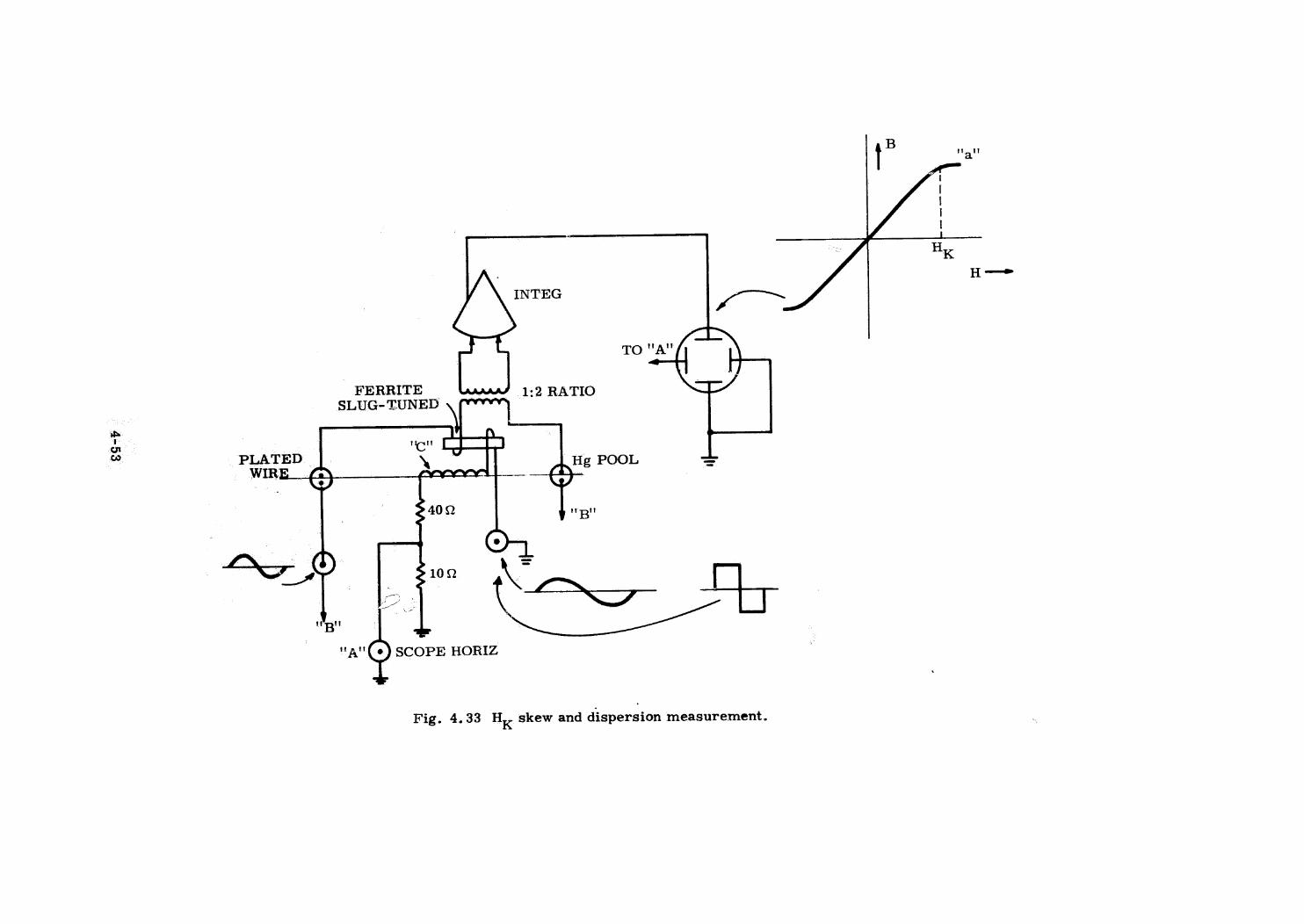
8S-F
INTEG
TO Wal
nd
FERRITE luw/ 1:2 RATIOSLUG-TUNED wr7 Non" ii
PLATED |mn
"A" SCOPE HORIZ
skew and dispersion measurement.Fig. 4.33 H,
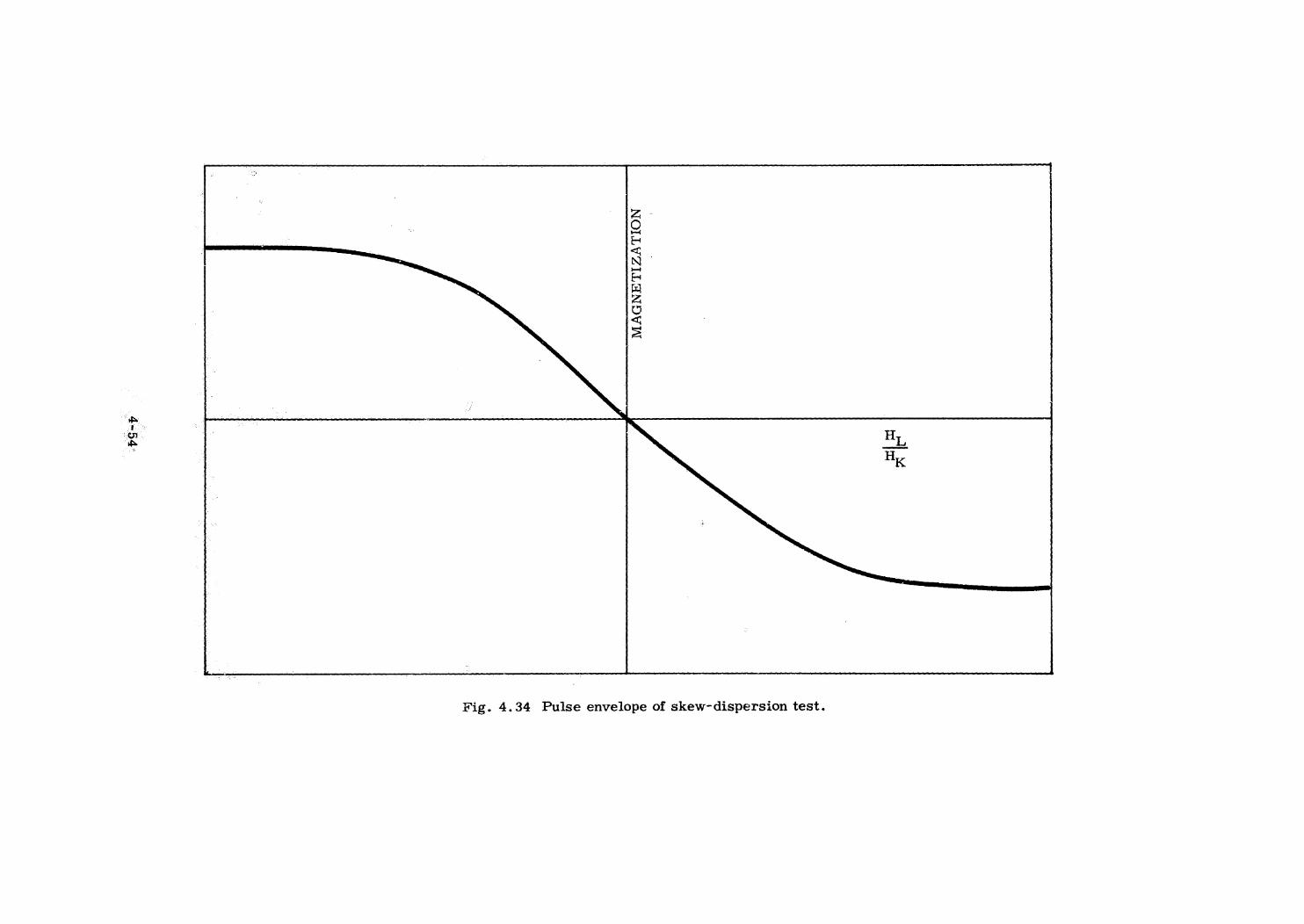
PSF
MAGNETIZATION
Fig. 4.34 Pulse envelope of skew-dispersion test.
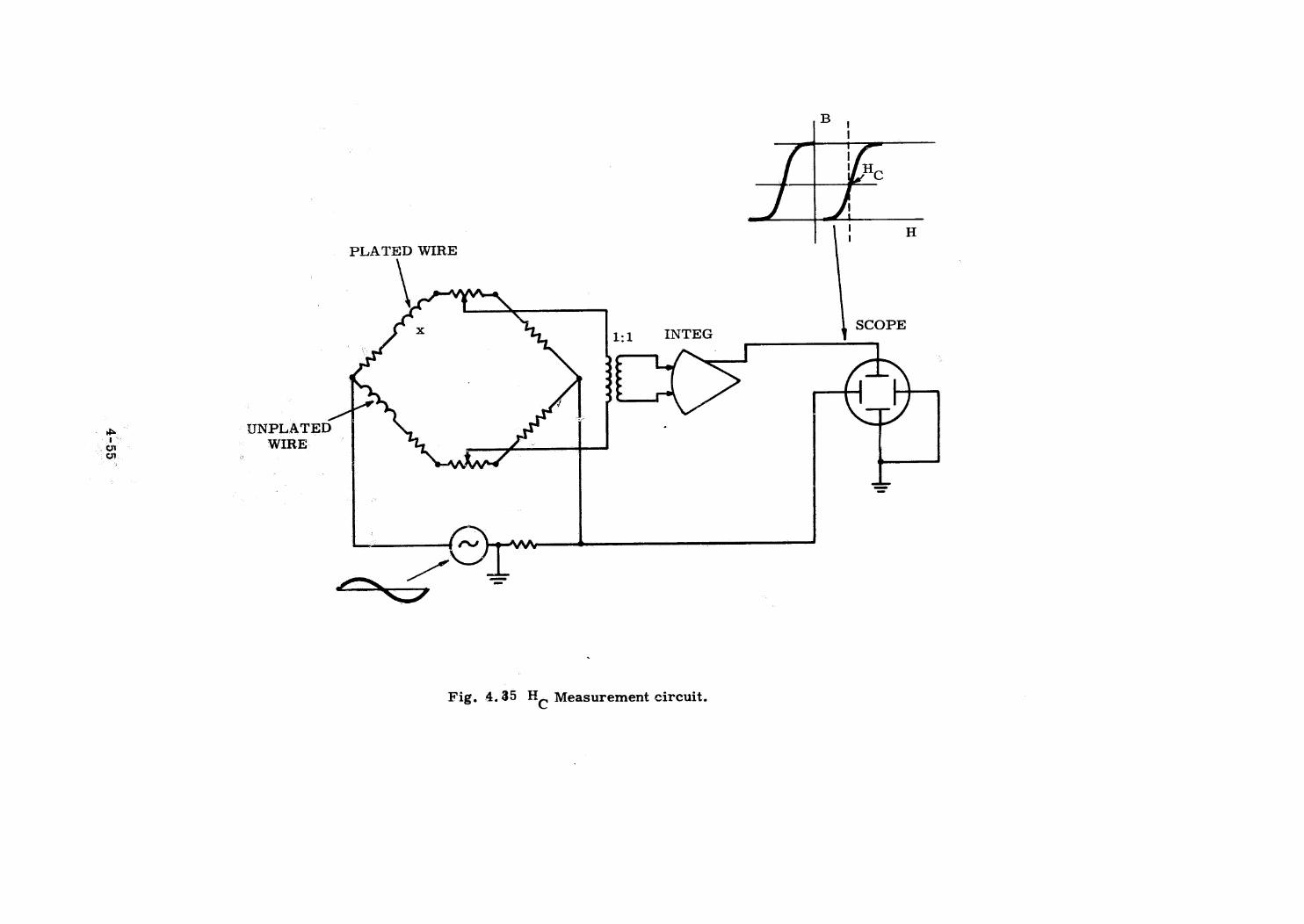
GS-F
—
UNPLATEDWIRE
PLATED WIRE
1:1 INTEG
ASh
aw VV
Fig. 4,35 Ba Measurement circuit.
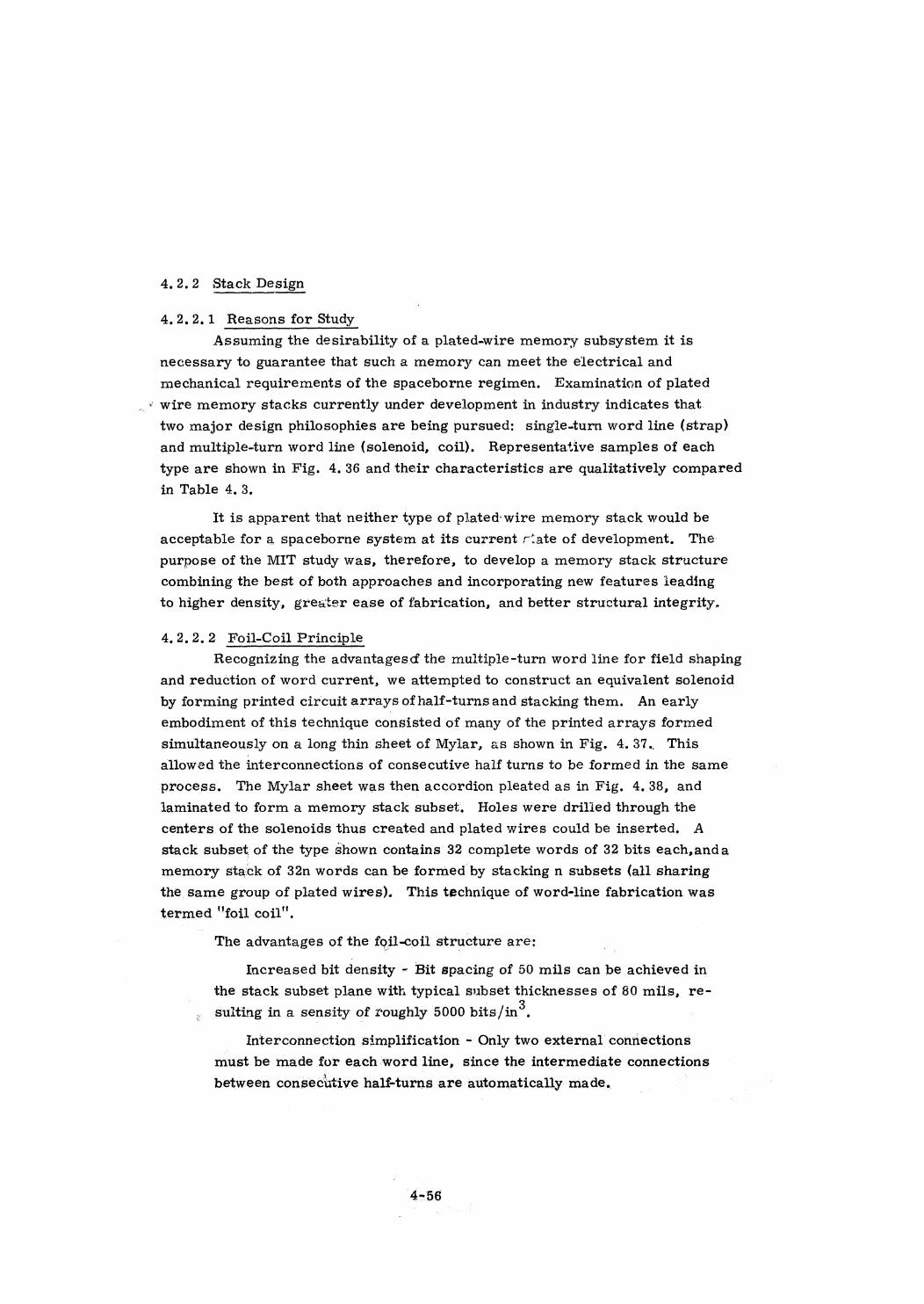
4,2,2 Stack Design
4.2.2.1 Reasons for Study
Assuming the desirability of a plated-wire memory subsystem it is
necessary to guarantee that such a memory can meet the electrical and
mechanical requirements of the spaceborne regimen. Examination of plated
“ wire memory stacks currently under development in industry indicates that
two major design philosophies are being pursued: single-turn word line (strap)
and multiple-turn word line (solenoid, coil). Representative samples of each
type are shown in Fig. 4.36 and their characteristics are qualitatively compared
in Table 4, 3.
It is apparent that neither type of plated-wire memory stack would be
acceptable for a spaceborne system at its current riate of development. The
purpose of the MIT study was, therefore, to develop a memory stack structure
combining the best of both approaches and incorporating new features ieading
to higher density, greater ease of fabrication, and better structural integrity.
4,2,2.2 Foil-Coil Principle
Recognizing the advantagesd the multiple-turn word line for field shaping
and reduction of word current, we attempted to construct an equivalent solenoid
by forming printed circuit arrays of half-turnsand stacking them. An early
embodiment of this technique consisted of many of the printed arrays formed
simultaneously on a long thin sheet of Mylar, «s shown in Fig. 4.37. This
allowed the interconnections of consecutive half turns to be formed in the same
process. The Mylar sheet was then accordion pleated as in Fig. 4.38, and
laminated to form a memory stack subset, Holes were drilied through the
centers of the solenoids thus created and plated wires could be inserted. A
stack subset of the type shown contains 32 complete words of 32 bits each,anda
memory stack of 32n words can be formedby stacking n subsets (all sharing
the same group of plated wires), This technique of word-line fabrication was
termed "foil coil".
The advantages of the foil-coil structure are:
Increased bit density - Bit spacing of 50 mils can be achieved in
the stack subset plane with typical subset thicknesses of 80 mils, re-
sulting in a sensity of roughly 5000 bits/ in®,
Interconnection simplification ~ Only two external connections
must be made for each word line, since the intermediate connections
between consecutive half-turns are automatically made. |
4-56
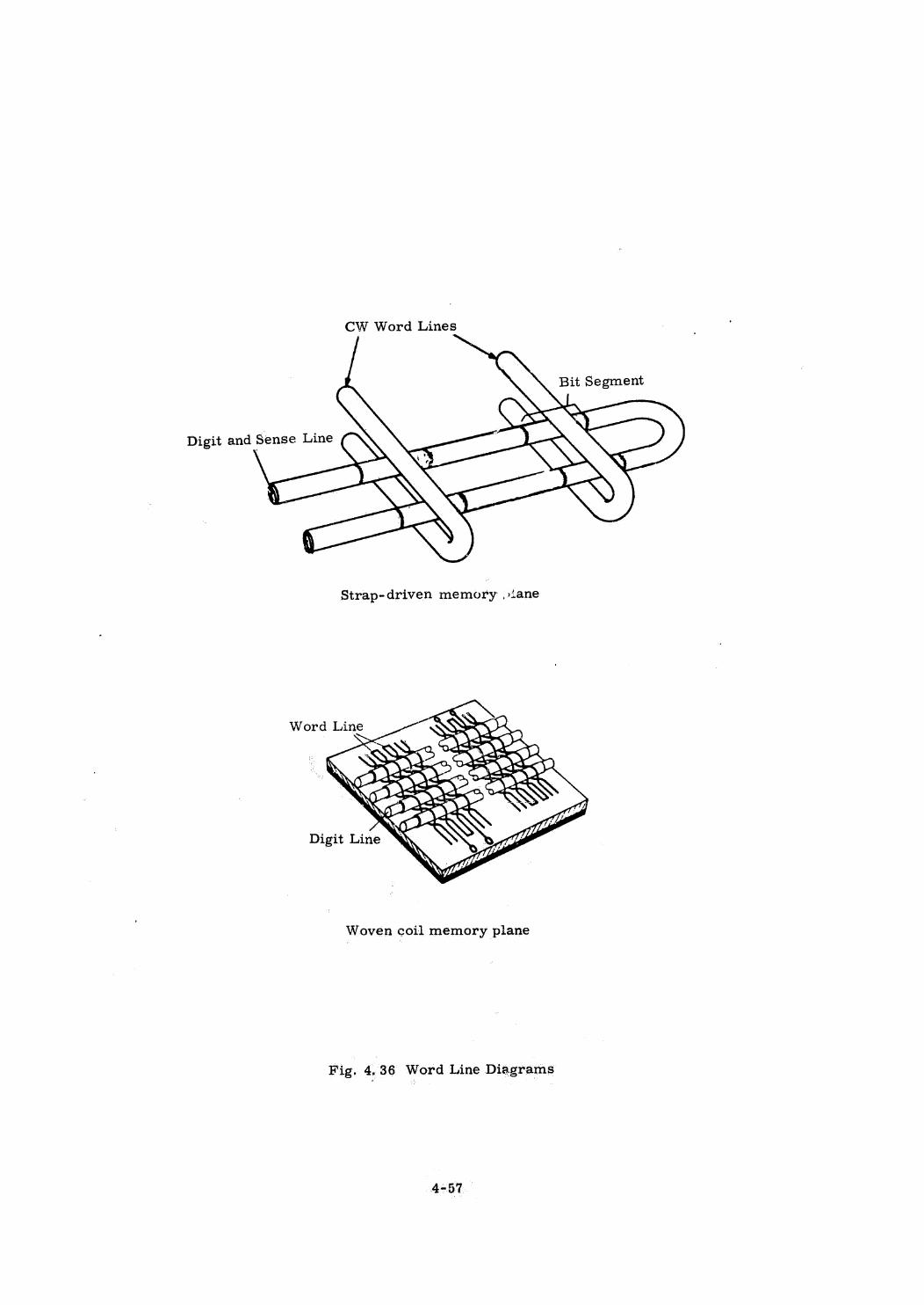
CW Word Lines
eeSegment
Woven coil memory plane
Fig. 4.36 Word Line Diagrams
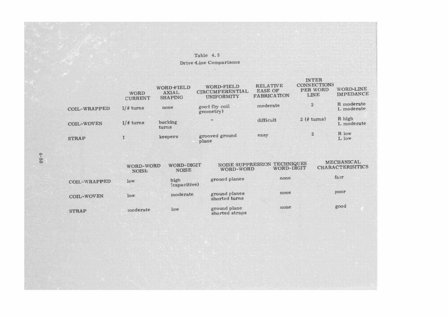
poos
goon
ait
SOLLISIUELOVUVHO“TIVOINVHOAN
eo
MOLU
Ssjerepow|]
udtyWy
aleaapoul7sieaepowlyy
SONVGadWISANTrauos
sdvaispeyous
guolaueydpunoisMOT
sun]pey10Us
auousaueidpunoissieiepow
(BaTyIOCED)
SuoUsauerdpunoidust
LIOTI-GuomGHYOM-CuONaSION
ajesepou
MOT
MOT
SSION
SHA@INHOGLNOISSHUddNSASIONLiplia-quomMGWHOM-CHOM
aueid
Astapunoispaacoissiadaay
suiny
(Suan)#)Zyous.gupong
c
NTT
(Aajeuical
gjeiepoul{rooAq)poorauou
NOIULVOTdaVaALUNUCAHINGONTGVHS
CHOMuadAOa@SVa‘1VILNSUGANONLVix
SNOLLOGNNOOSALLY120CO1Ts1a-duOMC(1aLtGHOM
UaLLNI
guosizeduio,)eureeAlig
6F31981
suany4/1
suini¢ii
INSHEDCeOm
dVuls
NSAOM-"TIOD
daddVurx-UC
dAValLs
NEAOM-TIOD
GaddVum-TOo
4-58
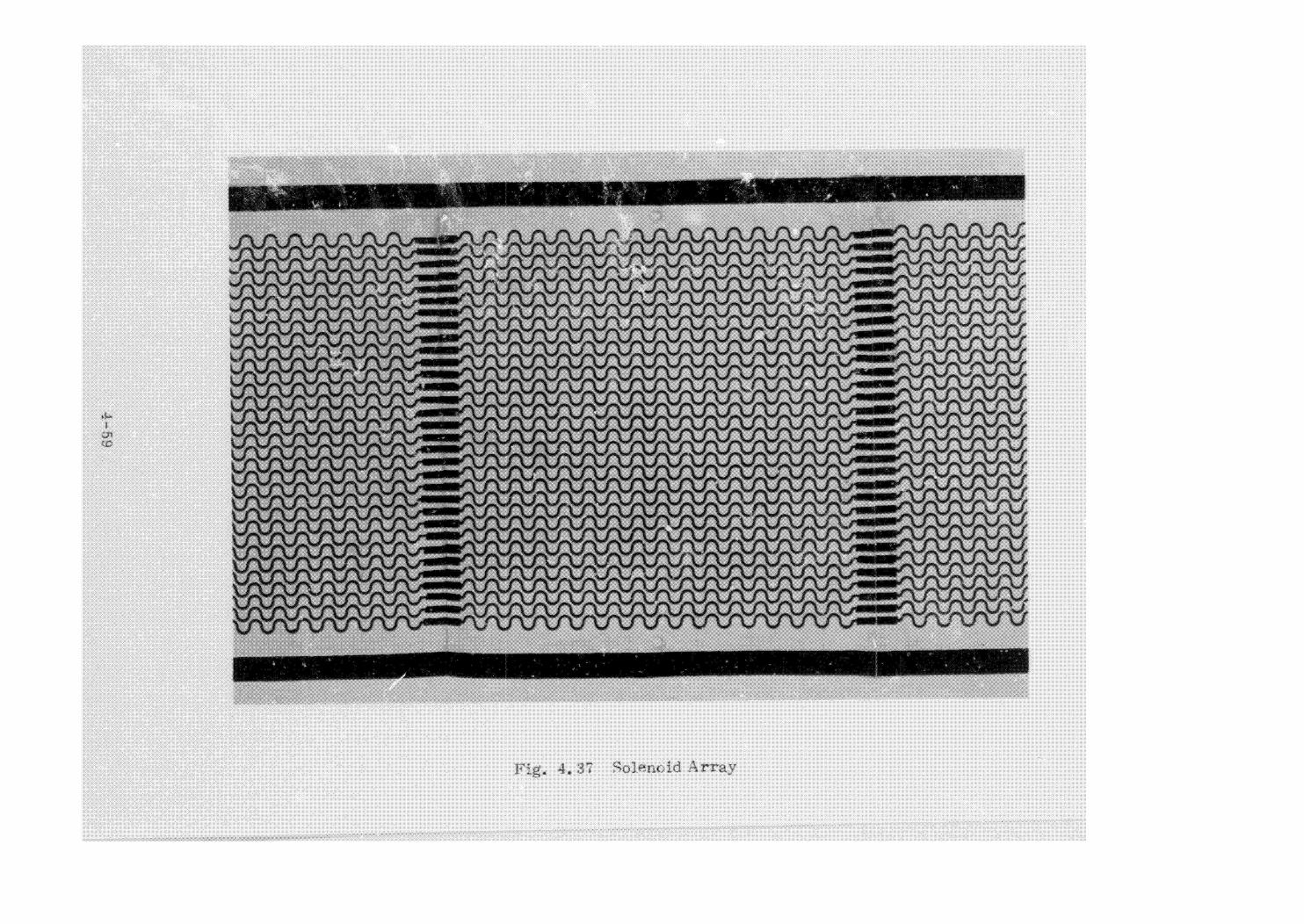
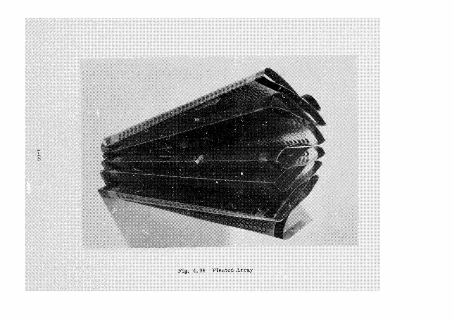
Fig. 1.38 Viected 4rruy
Ease of fabrication - Stack subsets may be tested on an individual
basis and plated wires need not be inserted until a complete stack
assembly has been made,
Structural integrity - A complete foil-coil stack is a rigid rectangu-
lar block requiring no further processing in order to tolerate severe
environments, o
4.2.2.3 Electrical Considerations
Preliminary investigation of the foil-coil stack subset uncovered several
noisé-coupling mechanisms which could affect memory performance.
A large scale model simulating a single-word coil was constructed and
probed with a gaussmeter to determine magnetic field strength variation along
the axis of the coil for various configurationsof normal direction turns and
opposed direction (bucking) turns. As expected, the addition of bucking turns
at the ends of the coil resulted in more rapid fall-off of field strength beyond
the ends of the coil with only a small reduction in field strength with the coil,
On the basis of this experiment, it was decided to construct the word coils of
the stack subset with single bucking turns at their ends. The resulting improve-
ment in field shape would allow for the desired high density of bits along the
plated wire while reducing unwanted bit-to-bit coupling. It was also noted that
ground planes could be inserted between stack subsets to further reduce coup-
ling should this prove necessary.
The mutual inductance oftwo adjacent word lines in a stack subset was
measured and found to be approximately 0,1 times the self inductance ofa
‘single word line, Consideration of the proposed stack configuration leads to
the conclusion that current coupling from a selected word line into the adjacent
lines can produce noise signals on the sense line. The polarities of these noise
voltages will be dependent on the information stored in the adjacent bits, and
therefore they will generally not cancel one another, However, the nonlinearity
of the relationship between drive current and rotation angle of the magntic
induction vector (and therefore between drive current and output voltage) indicates
that the magnitude of such a noise voltage should be less than (0. 1)” of the desired
output amplitude, This noise level should be insignificant.
Initial attempts to functionally operate a plated-wire bit in a stack sugset
“revealed a more serious problem. Since the word coil has non-zero impedance
and is distributed along the axis of the plated wire, an applied drive current .
develops a voitage drop along the coil, and this voltage difference couples into
the plated wire through parasitic capacitance. Theproblem is aggravated by
4-61
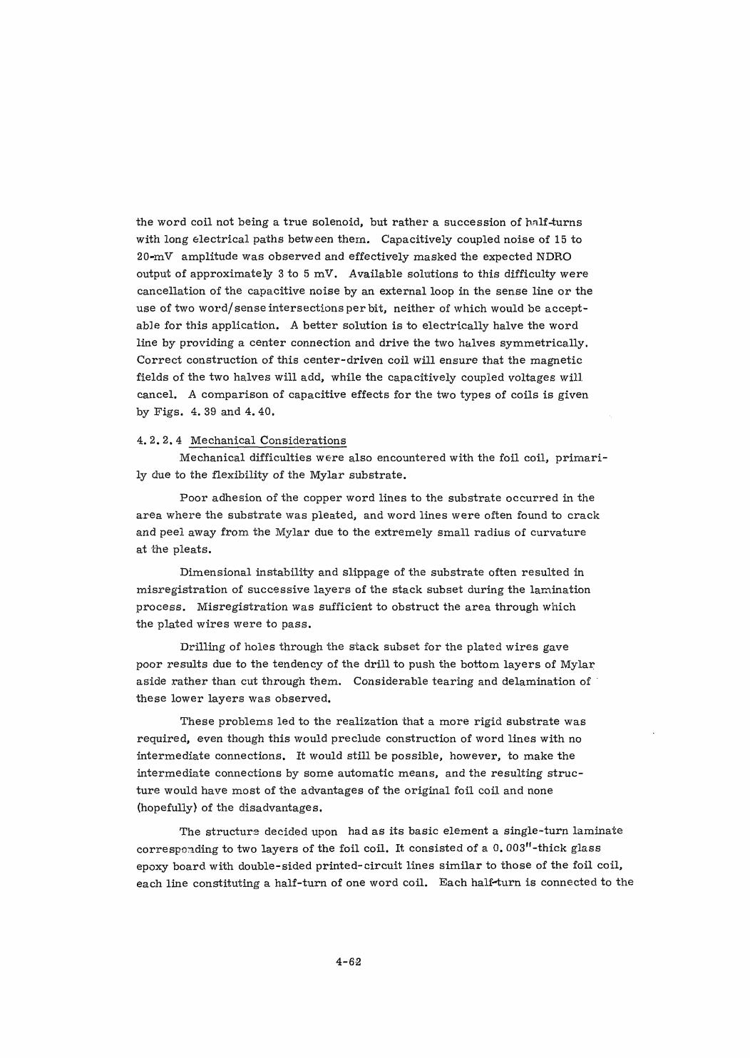
the word coil not being a true solenoid, but rather a succession of half-turns
with long electrical paths between thern. Capacitively coupled noise of 15 to
20-mV amplitude was observed and effectively masked the expected NDRO
output of approximately 3to 5m¥V. Available solutions to this difficulty were
cancellation of the capacitive noise by an external loop in the sense line or the
use of two word/sense intersections per bit, neither of which would be accept-
able for this application. A better solution is to electrically halve the word
line by providing a center connection and drive the two halves symmetrically.
Correct construction of this center-driven coil will ensure that the magnetic
fields of the two halves will add, while the capacitively coupled voltages will
cancel, A comparison of capacitive effects for the two types of coils is given
by Figs. 4.39 and 4. 40,
4,2.2,4 Mechanical Considerations
Mechanical difficulties were also encountered with the foil coil, primari-
ly due to the flexibility of the Mylar substrate.
Poor adhesion of the copper word lines to the substrate occurred in the
area where the substrate was pleated, and word lines were often found to crack
and peel away from the Mylar due to the extremely small radius of curvature
at the pleats.
Dimensional instability and slippage of the substrate often resulted in
misregistration of successive layers of the stack subset during the lamination
process. Misregistration was sufficient to obstruct the area through wiich
the plated wires were to pass.
Drilling of holes through the stack subset for the plated wires gave
poor results due to the tendency of the drill to push the bottom layers of Mylar
aside rather than cut through them. Considerable tearing and delamination of ©
these lower layers was observed,
These problems led to the realization that a more rigid substrate was
required, even though this would preclude construction of word lines with no
intermediate connections, It would still be possible, however, to make the
intermediate connections by some automatic means, and the resulting struc-
ture would have most of the advantages of the original foil coil and none
(hopefully) of the disadvantages.
The structure decided upon had as its basic element a single~turn laminate
corresponding to two layers of the foil coil. It consisted of a 0. 003"-thick glass
epoxy board with double-sided printed-circuit lines similar to those of the foil coil,
each line constituting a half-turn of one word coil, Each halfturn is connected to the
4-62
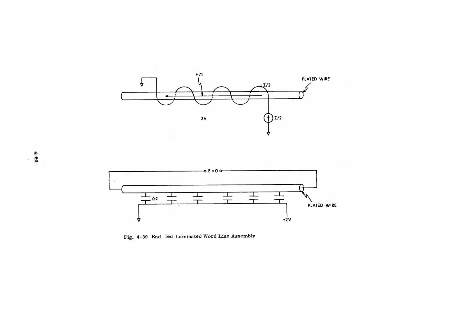
| PLATED WIRE<1/2
( < z + i i T | (
NY XQ? NU?
2v 1/2
o£=00
( a a Le 1 1
CS or xr xc x \\| | PLATED WIRE
| +2V
Fig. 4-39 End fed Laminated Word Line Assembly
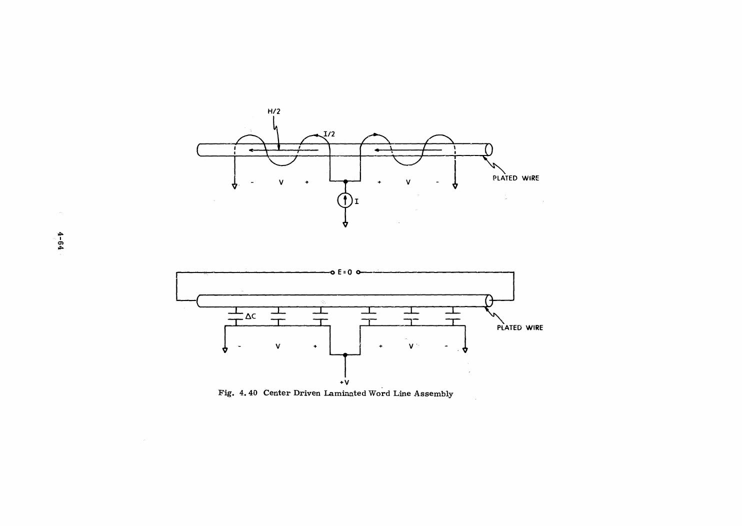
—e9-b
‘@ { - Ht 0| QS? 7 ]
t _ V . . V 7 | PLATED WIRE
:
oO E=0 o—
—( G—tac lL lL —_L —_lL —
_1 CC ~“C “tT mt __l_ PRATED WIRE
| ~ V * , * V ~ |
+V
Fig. 4.40 Center Driven Laminated Word Line Assembly
corresponding half-turn on the other side of the board by meansof a plated-
through hole at one end, The other ends of the halfturns are tinned. Plan
and section views of a single-turn laminate are shownin Fig, 4. 41.
A laminated word-line assembly is formed by laminating together
as many single-turn laminates as desired, using a 'B" stage epoxy for insula-
tion between laminates except in the areas previcusly tinned. The tinned areas
of adjoining laminates fuse into one another, and the entire assemb}jy becomes
the equivalent of a stack subset, witt electrical continuity through the assem-
bly as shown in Fig. 4. 42,
These laminated assemblies are then drilled and stacked in the same
way that the foil-coil subsets were to form a memory stack. An actual lami-
nated assembly is shown in Fig. 4,43, anda proposed 1024 X 32 stack with
integral electronies is shown in Fig. 4, 44,
Artwork has been generated for, and some double-sided and laminated
boards fabricated to the coil configuration with bucking turns. Sylvania,
Needham, has been accomplishing these tasks. Two problems were apparent.
Sylvania has been encountering serious difficulty in maintaining layer-to-layer
registration and has suggested that it would be unrealistic to hope for any level
of production of the laminates with the existing tolerance requirements, although
some boards with acceptable registration have been produced, (Close examina-
tion of the holes in the assembly of Fig. 4.43 reveals misregistration in that
board.)
In additicn, the reliability of the solder-plated layér-to-layer inter-
connects was questionable as there were major variations in the resistances
of the word lines within a board,
For these reasons, it was decided to stop work on the existing con-
figuration and consider a redesign based on more realistic estimates of the
tolerances that could be met in a laminate of this complexity.
A vendor was selected, General Components, Inc., St. Petersburg,
Florida, who had demonstrated good performance in the generation of com-
plex multilayer boards requiring accurate etching and laminate registration.
This vendor has been contacted to generate new artworkfor a center- driven
coil (six turns plus two bucking turns) and may subsequently be chosen to
manufacturea pair of boards. The new artwork will also incorporate changes
allowing for a loosening of the registration tolerances,
4-65.
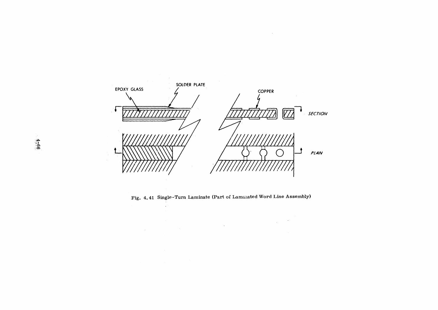
, SOLDER PLATE
fe
| Wo pe SECTION
TITUUTTL
— praw
Fig. 4.41 Single-Turn Laminate (Part of Lamimated Word Line Assembly)
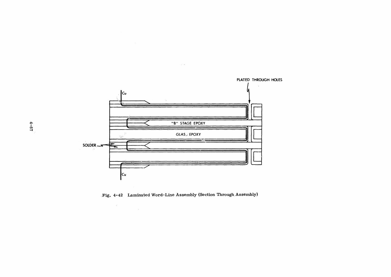
LO-P
SOLDER
PLATED THROUGH HOLES
_qCu
“BY STAGE EPOXY
GLAS.’ EPOXY
Cu
Fig. 4-42 Laminated Word-Line Assembly (Section Through Assembly)
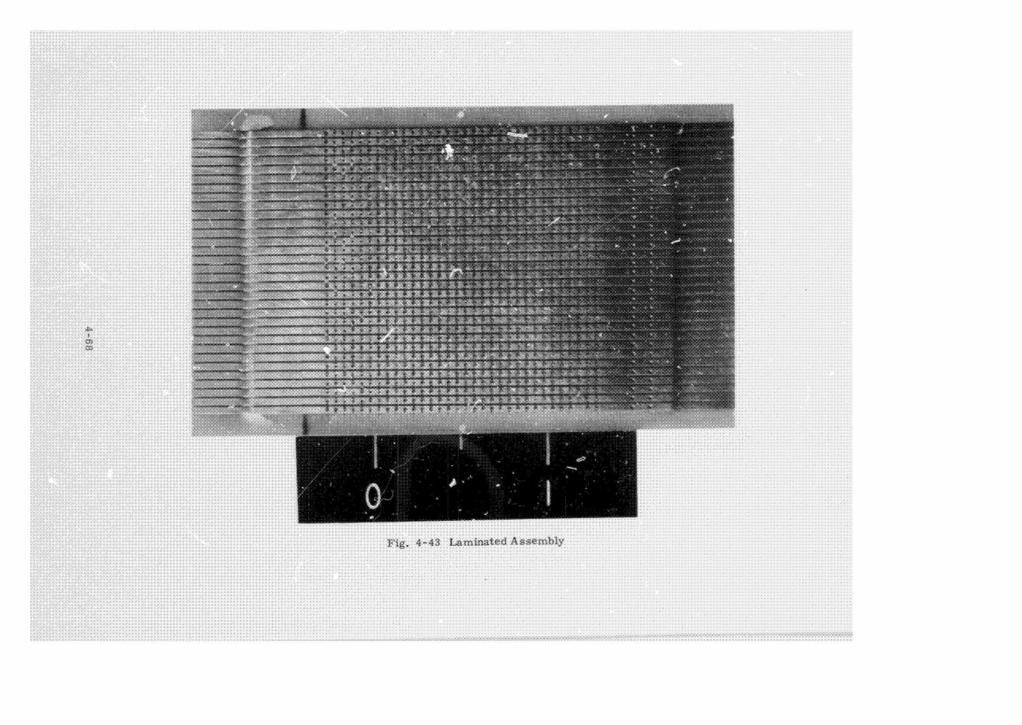
<SRS
—aSoS
oOCEESCo
Fig. 4-423 Laminated Assembly
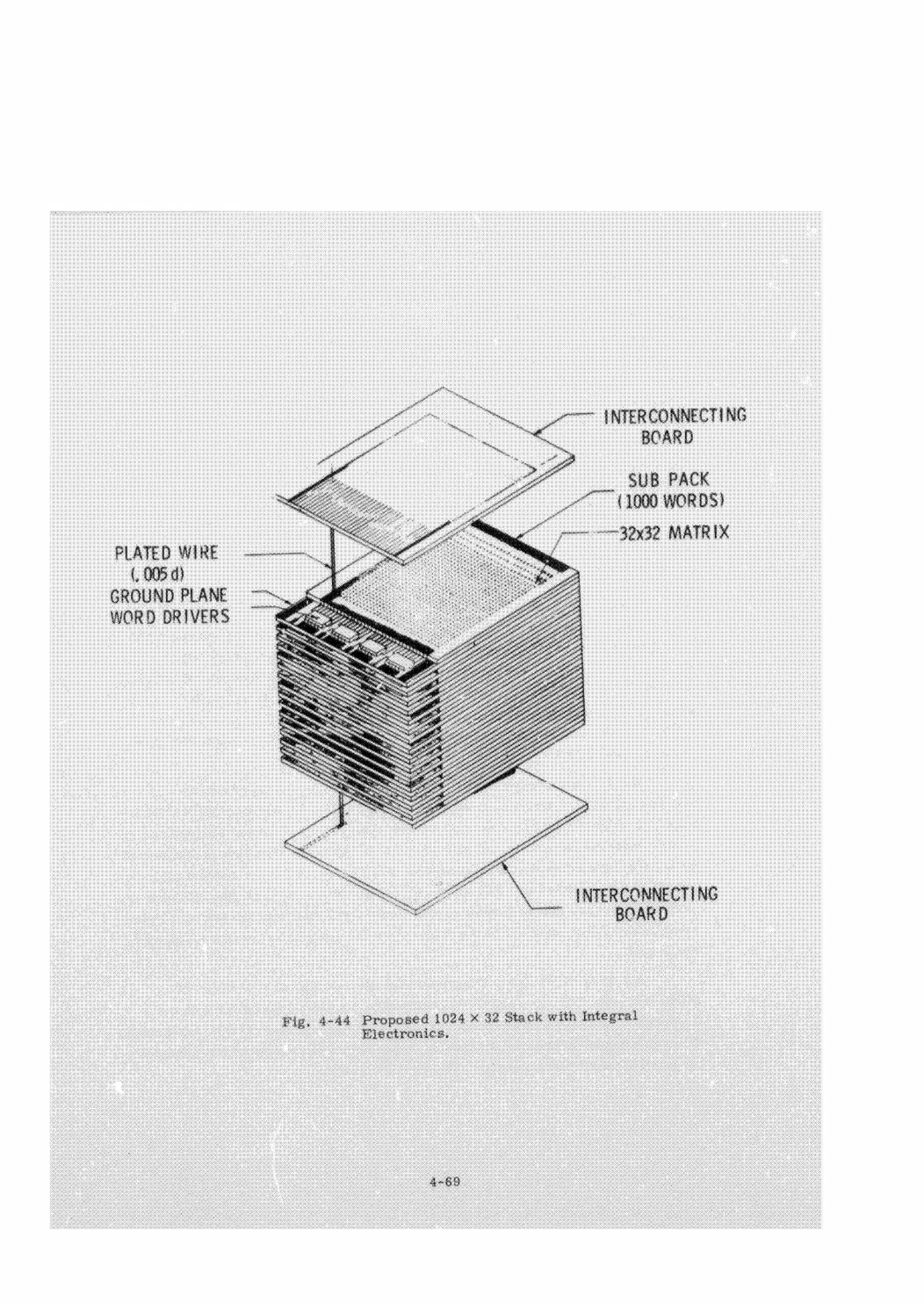
Serious thought is also being given to the two other major aspects of
assembly of a functional memory stack: interconnection of the plated wires
once they have been inserted into the stack, and mechanical design for those
portions of the memory electronics which could advantageously be incorporated
with the stack. One approachto the first aspect (tnin kapton-copper etched
circuits) has been tried with limited success. For the second aspect, it
appears that a sufficient portion of the memory address selection electronics
to greatly reduce the numberof external stack connections can be integrated
with the stack, and that this circuitry, in currently available microcircuit
flat packs, would be mechanically compatible with present or proposed stack
configurations,
Further activity is contingent upon the receipt of the new configuration
board and its testing.
4.2.3 Circuit Design
4.2.3.1 Driving Circuits
In the absenceof a functional stack of MIT design, circuit development
has been conducted with a memory stack of similar electrical properties
manufactured by Toko, Inc. and the Librascope Division of General Precision,
Inc, The same general guidelines of using integrated circuits as much as
possible and incorporating portions of the electronics into the stack assem-
bly were followed even though the Toko-GPL stack was several times the size
of the proposed MIT design.
| Speed considerations dictate the use of an all-transistor memory
address selection scheme consisting of a squgre (2° x 2°) array of NPN transis-
tors with bases bussed by rows and emitters bussed by columns. Collectors con-
nect to individualword-drive lines in the stack. Address selection is perforrned
by activiating a current source connected to one base bus and a current sink con-
nected to one emitter bus. The single transistor at the intersection of these two
*, orthogonal busses will be turned on and current will flow through the associated
word line, causing each bit of that word to be readonto the corresponding digit/
senseline.
A survey of available integrated circuits resulted in the choice of
SUHL (SylvaniaTTL) as capable of performing all needed functions withthe
exception of acting as emitter-bus current sinks (insufficient current capability).
For convenience in breadboard circuit design they were procured from Sylvania
on small prinied-circuit boards called Syl-Pac cards. .
4-70
A block diagram of the complete memory drive system is given in
Figs. 4.45 and 4.46, the former showing all of the SUHL circuitry and the
discrete transistor emitter switches, while the latter illustrates a portion of
the square array of selection transistors (also discrete for the breadboard).
The memory address register (MAR) consists of two Syl-Pac cards,
each containing two 4-bit counters. All of these are cascaded to form a
single 16-bit counter, which can be pulsed to run the selection system
sequentially through all memory addresses, Alternatively, a control switch
exists which is capable of causing a bank of sixteen data switches to be strobed
into the MAR for loading a preset address. The MAR contents are displayed
by a bank of sixteen indicator lamps driven from the MARthrough the MAR
display drivers. .
The lowest five bits of the MAR are used for emitter-py.s selection.
Bits 1-3 and their complements go to two Syl-Pac cards containing a total
of four independent 8-line decoders, called emitter decode JI. Bits 4-5 go to
one-half of a similar card, emitter decode I, which does a one-out-of-four
selection to determine which of the II-level decoders is activated, All emitter
decode-II outputs are inverted by the emitter switch drivers and 32 discrete
transistors (emitter Switches) are driven by the inverters and act as emitter-
bus. current sinks.
Bits 6-10 of the MAR are used in an identical manner for base bus.
selection with one difference. Here the base bus drivers are high-power line
driversrather than low-powerinverters and the base busses are driven
directly from the integrated circuits.
The unused inputs at the decode-I level are used for timing to ensure
coincidence of base and emitter bus pulses and eliminate logic noise,
The SUHL circuitry has performed satisfactorily and has sufficient
speed capability for any anticipated memory requirements, Difficulty has
been encountered in the selection transistor array due to operation of these
transistors close to their maximum ratings and due to unexpectedly high
capacitances of the base and emitter busg¢s. Workis in progress to eliminateot
these difficulties.
In anticipation of the needs of the MIT design stack, conferences with
semiconductor vendors have indicated no apparent problems with integrating
the selection transistor matrix, and conventional flat packs containing groups of -
eight transistors suitably interconnected have been ordered. These would be
incorporated withthe MIT stack as shown in Fig, 4, 44.
AW
La DATA SWITCHES MAR DISPLAY¥
MAR CONTROL SWITCHES
MAR DISPLAY DRIVERS
cath _MAR CONTROL LOGICAND TIMING |
Tit ris
a 5ee es eeeCos
uy1
MEMORY aDones REGISTER (MAR]j
EMITTER | BASEDECODEI DECOODE T
ss. «vy 2
_¥.——
¥
¥ et \
EMITTER DECODE I 1J
BASE DECODE I
i
EMITTER SWITCH DRIVERS ‘BASE Buss DRIVERS
[ J J
EMITTER SWITCHES
TO MEMORY STACKEMITTER BUSSES
|||||¢
Fig. 4.45 Memory Drive Logic
4-72
TO MEMORYSTACKBASE BUSSES
Qaaeweoeww
* VOLTAGE
YPLANE #3 /
4 A ”
4 q 4
4 4 4
1 A.
PLANE #2 7 tfJ) 4 @ q
4 44 4
= rPLANE #1 t | /
, $. $3 7
4 . 4 q
3
ae
tute
wee 4
EMITTER-3USS ; BASE BUSS
BASE BUSSDRIVERS
EMITTER SWITCHES
Fig. 4.46 MemoryDriveConfiguration
— 4-730
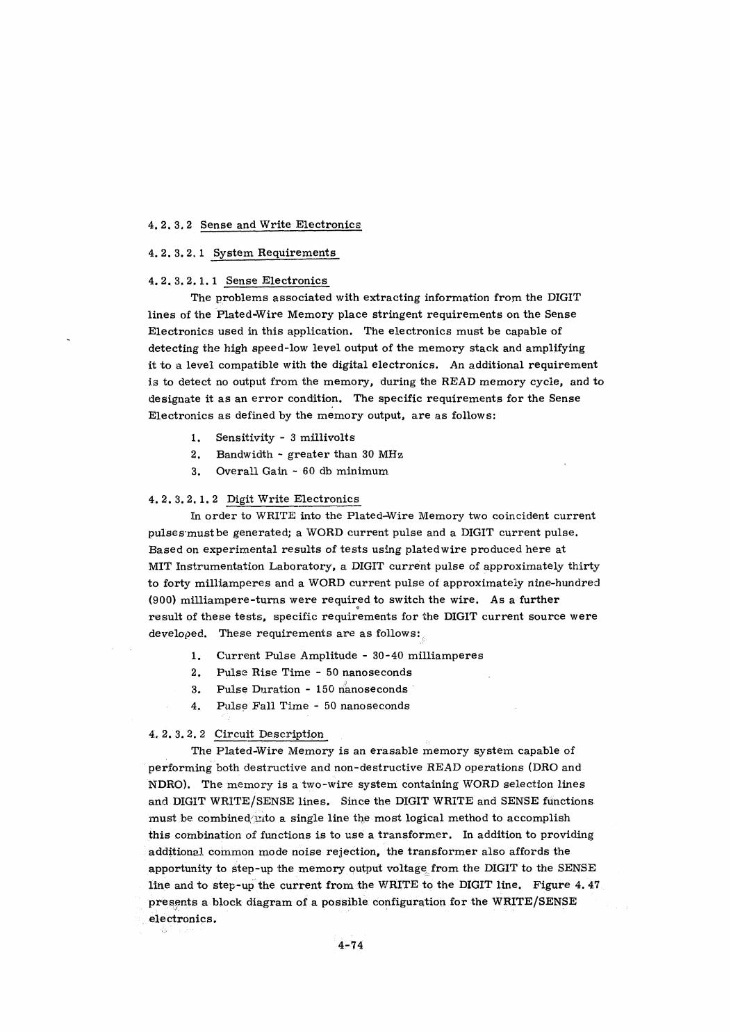
4.2.3.2 Sense and Write Electronics
4,2,3.2.1 System Requirements
4,2.3.2.1.1 Sense Electronics
The problems associated with extracting information from the DIGIT
lines of the Plated-Wire Memoryplace stringent requirements on the Sense
Electronics used in this application. The electronics must be capable of
detecting the high speed-low level output of the memory stack and amplifying
it to a level compatible with the digital electronics. An additional requirement
is to detect no output from the memory, during the READ memory cycie, and to
designate it as an error condition. The specific requirements for the Sense
Electronics as defined by the memory output, are as follows:
1. Sensitivity - 3 millivolts
2. Bandwidth ~ greater than 30 MHz
3. Overall Gain ~ 60 db minimum
4.2,.3.2.1.2 Digit Write Electronics
In order to WRITE into the Plated-Wire Memory two coincident current
pulses‘mustbe generated; a WORD current pulse and a DIGIT current pulse.
Based on experimental results of tests using platedwire produced here at
MIT Instrumentation Laboratory, a DIGIT current pulse of approximately thirty
to forty milNamperes and a WORDcurrent pulse of approximately nine-hundred
(900) milliampere-turns were required to switch the wire. As afurther
result of these tests, specific requirements for the DIGIT current source were
developed. These requirements are as follows: .
Current Pulse Amplitude - 30-40 milliamperes
2. Pulse Rise Time - 50 nanoseconds
3. Pulse Duration - 150 nanoseconds ©
4, Pulse Fall Time - 50 nanoseconds
4.2.3.2,2 Circuit Description
The Plated-Wire Memory is an erasable memory system capable of
performing both destructive and non-destructive READ operations (DRO and
NDRO). The memoryis a two-wire system containing WORD selection lines
and DIGIT WRITE/SENSE lines. Since the DIGIT WRITE and SENSEfunctions
must be combinedsito a single line the most logical method to accomplish
this combination of functions is to use a transformer. In addition to providing
additional common mode noise rejection, ‘the transformer also affords the
apportunity to step-up the memory output voltagefrom the DIGIT to the SENSE
line and to step-upthe current from the WRITEtothe DIGIT line. Figure 4. 47
presents a block diagram of a possible configuration for the WRITE/SENSE
; electronics. | |
“4-74
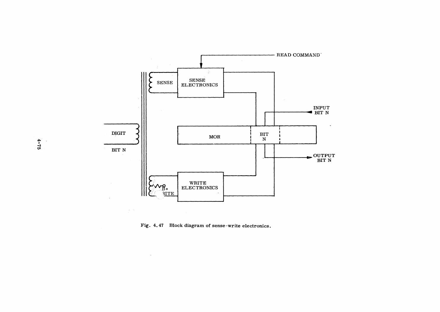
SL-%
BIT N
Fig. 4.47 Block diagram of sense-write electronics.
!
SENSE
READ COMMAND
SENSEELECTRONICS
INPUT~@ BIT N
T 7| pr!1MOR tNi l
OUTPUT* “BIT N
WRITEELECTRONICS
4,2.3,2,.2.1 SenseElectronics
The Sense Electronics contains a Gating or Limiting network, a Linear
Wide-Band Amplifier and a Threshold Detection and Level Conversion circuit.
Two designs currently exist for the Sense Electronics, These designs differ
in the technique used to prevent amplifier saturation and the selection of the
linear amplifier used to amplify the output signal. Because the merits of each
design have not been fully evaluated, a recommendation as to which will pro-
vide the best performance cannot be given at this time. However, in order
to make this discussion as complete as possible, both designs wiil be presented
although no trade-off of their relative advantages will be undertaken, Figure 4, 48
shows both design alternatives.
4,2.3.2.2.1,1 Limiting Circuit/Gating Circuit
The following two. subsections describe two alternate methods for pro-
tecting the linear amplifier from saturating during the WRITE memory cycle
and increasing the total memory cycle time. The designs are shown in
Fig. 4.48. However, it should be noted that either of the designs may be used
with either linear amplifier design.
4,2,3.2.2,.1.1.1 Limiting Circuit
The Limiting Circuit shown in Fig. 4.48A protects the amplifier from
saturating by limiting the input-signal excursion of the WRITE current pulse to
plus or minus the forward voltage drop of the diode, During the READ memory
cycle, the output voltage from the stack is substantially less than the voltage
necessary for the diode to conduct, and therefore the lead on the SENSEline is
the two current-limiting resistors in series with the parallel combination of the
amplifier input impedanceand the junction capacities of the diodes,
4,2,3.2,.2,1,1.2 Gating Circuit
The Gating Circuit prevents the linear amplifier from saturating by
having reversed-biased diodes in.ceach of the differential inputs during the
WRITE memory cycle. During the READ cycle the diode bridge networks are
forward-biased by enabling the bias supplies,and the input signal is transmitted
to the amplifier with no differential error.in amplituderesulting (i.e. since it
is a balancednetwork, by Kirchhoff's law the sum of the veitages around all
three of the closed loops must equal zero. ) |
4,2,.3.2,2,1.2 Linear Amplifier
The function of the linear amplifier is to detectthe differential input
signal and amplify it to a level compatible with that of the MECL current-mode
logic gate, The amplifier, to perform the required task, must have a minimum
differential gain of 33 db and a minimum band width of 30 MHz.
422.6
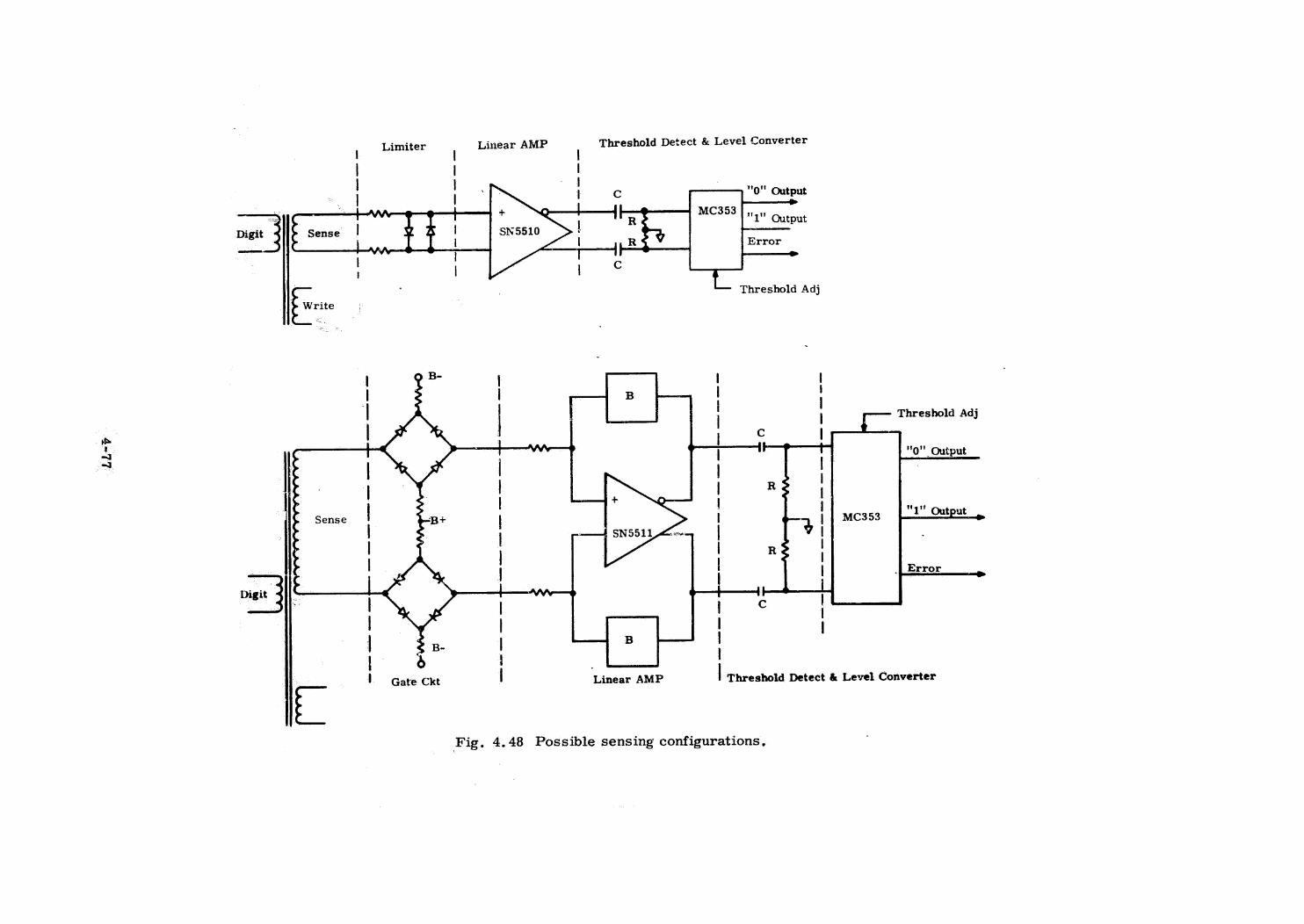
LLF
-
Limiter Linear AMP Threshold Detect & Level Converter
||
| tatt
| Cc 0" Output
f | MC353 ,. T Watti R 1” Output
| R Errorpesca
Cc L Threshold Adj
| |B |
{ Threshold Adj| | f
| |$——1 .r
| i| "oO" Output
¢ || R
>l | "1" Output
¢ I || Mc353
}
Outpt
¢ | |¢ | R |
it ! |—y11¢ | .LError
SHC: | .Digit 2 _
—I| | | ; || | | l
| B || |
i | Gate Ckt | Linear AMP | threshold Detect & Level Converterbb>>
ee Fig. 4.48 Possible sensing configurations,
4.2,3.2.2.1.2.1 SN 5510 Wide Band Video Amplifier
The Texas Instruments SN-5510 deviceis a wide-band video amplifier
having differential outputs and inputs. This unit features a flat frequency
response from dcto 40 MHz and a typical midband gain of 40 db. This amplifier
has a permissable gain variation of 38.2 db to 44.1 db and, while the amplifier
provides the necessary amplification,it is desirable to reduce the gain varia-
tion for this application. Attempts to reduce the gain variation of this device
by application of a feedback network proved unsuccessful. The unsymmetrical
gain characteristics of each half side of the double-ended amplifier, the inability
to provide interstage frequency compensation, and the large de off-set voltages
existing between the outputs and inputs were the reasons for the amplifier
instability with the application of the feedback network, However, a suitable
gain adjustment can be instituted into another portion of the design to compen-
sate for gain variations.
4,2,.3,2,2,1.2.2, SN-5511 Wide-Band Differential Amplifier
The SN-5511 device is a wide-band amplifier with differential outputs
and inputs and featuring low dec off-set voltages and the ability to provide inter-
stage frequency compensation making this device useful in closed-loop configura~
tions. Ina closed-loop configuration, a differential voltage gain of 36 db will
result in a 30 MHz bandwidth. In addition, through the use of reactive compon-
ents in the feedback networks, an active bandpass filter can be formed to limit
extraneous noise and make the circuit more selective.
Construction of a breadboard circuit which would satisfy the system
requirements has not been completed. However, the amplifier has. been operated
in a closed-loop configuration (resistive networks only) with the approximate
gain and bandwidth required, Since this is a newly announced circuit, informa-
tion on gain and bandwidth variations which could be expected with this device
is not presently available.
4,2,3.2.2.1.3. Threshold Detect and Level Converter
The function of the Threshold Detect and Level Converter is to establish
a reference level for comparison with the memory output signal, and upon the
reference being exceeded, during the READ command time, to convert the
memory output signal ("i"' or "0") to a level compatible with thedigital logic
levels of the system. The circuit contains a single-pole high-pass RC filter
newtwork and a MECL gate, The RC network provides dc isolation between
the amplifier output and the MECLgate inputs. In addition, this circuit in
conjunction with the roll-off of the amplifier forms a bandpass filter around
4-78
the frequency of interest. The type MC-353 MECL gate is an integrated cir-
cuit half-adder. Reference potentials (positive and negative) are applied to
two of the input terminals. When either of these levels is exceeded during
the READ command time an output is transmitted to the Memory Operarid
Register (MOR). Since the memory output signal is symmetrical, if during
the READ command time neither reference level is exceeded,then an error
condition exists and this circuit will transmit an error indication. Figure 4, 49
presents the signal waveforms and the truth tabié and logic equations for the
MECLgate.
4,2.3.2.2.2 Digit WRITE Electronics
Figure 4, 50 presents the Digit Write Electronics. The function of this
circuit is to generate the appropriate current pulses for storage of the contents
of the Memory Operand Register (MOR) in the Plated-Wire Memory. This
function is accomplishedin the following manner.
The WRITE command enables one of the two integrated-circuit gates,
which in turns enables one of the two saturating transistor amplifiers. Depending
on which of the two amplifiers is enabled and its polarity with respect to that
of the transformer, a positive or negative current will be induced into the Digit
winding of thememory.
4.2.3.3 Testing Equipment Design
The following two pieces of major test equipment have been built for use
in plated wire memory stack development.
4,2.3,3.1 Memory Exerciser
The main feature cf the memory exerciser is a multifunction 12-bit
address register (AR) with an octal display, which has the following modes of
operation:
A. Counting
1. Up/down
2. Continuous/single step
3. Normal/disturb
B, Special
1. Preset
2. Compare
4-79
oo GH it Al
a
A | " CO
on =
il Al
A,
al4
Z=P |N ———-+}10 4}+-—_}-E st)
P, ST7,8
oo o1 11 10oo 111 o10 010 o10
ST,N 01- 001 000 000 0009,10 11 001 000 000 000
10 001 000 000 000
E, W, Z4,5,6
+ Threshold
- AmplifierOutput
- Threshold
read
Fig. 4.49 Truth table for sensegate. |
4-80
Digit Me
Fig. 4.50 Digit write electronics.
4-81
Mor Bit N
- Mor Bit N
Write
4, 3
The counting modes are non-exclusive and are self-explanatory with
the exception of disturb. Disturb is an oscillatory mode about an arbitrary
address, A, such that the time sequence of addresses in the ARis A, A-1,
A, Ati, A, A-1, etc. This mode is used forworst-case disturb tests of plated-
wire memory bits.
The preset mode loads an address manually entered by a toggle-switch
register into the AR. This address will either remain in the AR or be used as
the starting location for a counting mode at the user's discretion. The com-
pare mode is a counting mode which automatically terminates at an address
set into another toggle-switch register. The compare-mcde toggle switches
allow bits of the address to be "don't cares", i.e., setting the switches to
ddd ddd 011 101 (d=don't care) will cause the AR to stop at 35. or 135, or
2354.etc, » whicheveris first encountered,
In addition to the AR, the memory exerciser contains read, write,
and digit-enable generators, allowing the exerciser to control memory drive
currents in synchronization with address selection.
A further feature is a bank of 32 data lights for display of the contents
of the selected address, and a data-switch register for altering the contents.
4,2,3.3.2 Programmable Pulse Sequencer
The sequencer consists of a 10-stage ring counter driven by a variable-
frequency clock. Each of the ten‘stages drives a vertical line of a ten-by-ten
diode plug board, Ten output channels consisting of two cascaded monostable
multivibrators are provided, A channel is activated by inserting a plug at the
required pulse time. The cascaded monostable multivibrators are provided
so that a pulse of variable width, displaced a variable time from the clock
pulse; may be obtained. Sufficient logic is provided so that any step in the
ring counter may be repeated an arbitrary numberof times under the control
of analog timers. This feature is useful in disturb testing. The range of
operation is 100 msec per step to 100 nanosec per step.
Integrated Circuits
4,3.1 Introduction
The task for integrated circuit development is a follow-on effort to the
work performed on integrated circuits for the Apollo Block I and Block I
Computers, The effort consists of a review of the state-of-the-art technology
and of the industry's ability to produce new devices. The investigation of the
new integrated-circuittechnologies includes the study of the new MSI & LSI
logic functions plus the new fabrication technology required to produce these
complex devices.
4-82
4,3.2 Bipolar Vs MOS Technology for LSI
As expected, both bipolar and MOS tezhnologies exhibit their respective
advantages and disadvantages.
MOSdevices have several inherent drawbacks:
1,
The
The MOStransistor is a field-effect device whose electrical
characteristic is dependent on surface oxides. The problem of
producing a stable oxide because of mobile ion contamination in
the gate oxide and oxide surface charge requires sophisticated
process control. Silicon nitride for gate oxides (MIS technology)
may present a future solution, but continuing long-term stability
investigations are still presently required for both MOS and MIS
technology.
MOStransistors exhibit low transconductance and high stray capa-
citance which cause them to be slow comparedto bipolar devices.
This disadvantage is partially overcome by
a. 4-phase clocking
b. increasing operating power
c. decreasing the voltage swings
diffusing complementary transistors on the same chip,
creative circuit design.
However, until a basic technology breadthrough occurs, MOS
transistors will exhibit longer switching times than bipolar devices.
The MOS transistor is highly susceptible to stray voltage. This
has been partially overcome by the thick-gate oxide (MTOS)transis-
tors and by sophistivated process control.
advantages of MOS devices are:
The bagic simplicity of MOS processing readily lends itself to large
scale integration (LSI). The most promising MOS LSI appears to be
in the memory area, Vendors arepresently building both read-
write and read-only memories using MOS LSI.
Potential low cost because of the basic simplicity of the manufac-
turing process.
Low power which enables high circuit density on one chip without
thepower limitations of high-speed bipolar devices. .
4-83
The disadvantages of bipolar LSI are:
1. Does not as readily lend itself to large scale integration as MOS. |
Several insulated layers of metal for interconnects have to be used ue
for the same complexity as a MOS circuit.
2. Bipolar manufacturing process is more complex than MOS,
3. Higher power operation is required,
4, Exhibits low input impedance.
The advantages of bipolar LSI are:
1. Bipolar transistors are faster than MOS.
2. Bipolar transistors are not as susceptible to surface state changes.
4.3.3 Failure Analysis & Failure Modes
The fabrication techniques of LSI will introduce new failure modesnot
previously detected. The multilayer metal system will be thinner and narrower
and more subject to corrosion, metal migration ani local heating. Multi-metal
systems have not been throughly evaluated. Smaller geometries will increase
etching problems aggravating contact resistance problems and metal-thinning
at oxide steps, Over-etching of the pyrolitic oxides will .damage the lower-level
metal layer. The long term stability of pyrolitic oxides must be investigated,
Failure analysis must become increasingly more sophisticated. X-Ray, thermal
and electron:probe techniques may hecwine routine analytical procedures.
Analysis of failéd parts will become a more time-consuming procedureto locate
faults and determine failure modes so that corrective procedures in the device
processing can be instituted.
4,3.4 Testing Electrical
The testing of LSI is still one of the unsolved problem; that is, effective
verification that a large number of gates (100 or more) are all operating
functionally and with sufficient noise and electrical margins. This is further
complicated by the consideration of the type of logic used, such as T?L, DTL,
ECL, RTL, etc.,each of which must be tested and evaluated differently. This
is compounded by the diversification of the circuit elements coupled with the
non-standardization of the circuit arrangement and fabrication technology being
usedby the different vendors. The numberof tests required to test a device isgm
circuit can assume. From this formula, it is seen that an astronomical num-
where n is the numberof inputs and m is the numberof states that the
ber of tests can be required, To resolve this problem, versatile, high-speed,
easily programmable testers coupled with well-conceived testing programs
are required,
4-84.
4,3.5 Environmental Testing
4.3.5.1 Marginal
Marginal testing - to detect marginal devices in a complicated circuit
array will require the versatility of the electrical test described above coupled
with an environment knownto differentiate between aspects of the logic cir-
cuit used. The most common type of environmental changes will be voltage,
temperature, input and output loading and noise. Unfortunately, each logic
type behaves differently under these environmental extremes, These environ-
mental tests will still not likely detect marginal devices degrading with time.
4.3.5.2 Environmental Evaluation Testing
An environmental test to destruction procedure will be required to
detect degrading parameters and latent faults. Since failure modes unique to
LSI are expected, completely new studies for environmental, thermal and
operational test to destruction are essential so that effective and non-destructive
screening and/or quality assurance procedures may evolve.
4.3.5.3 Screening
Because of the complexity of LSI, a radically new approach to screening
and quality assurance is necessary. i’resent screening procedures depend on
component parameter measurements which will no longer be available for
LSI testing. For example,variables data, a technique used to detect degrading
components, will be meaningless. The ratio of the cost of assuring the quality
and reliability of each LSI part to the procurement cost must increase if only
‘because of the extensive electrical tests required. «’
4.3.6 Packaging & Interconnects
Any packaging and interconnect scheme must maintain the speed ad-
vantages inherent in LSI. The principal advantage of LSI to military and space
programsis low coupling capacitance between gates, which creates higher
speed-power ratios, The lower powerat speed aids high packing densities and
and economy of deéep-space operation.
Package standardization has not been resolved for LSI circuitry, Depend-
ing on the circuit complexity and the computer organization, the gate-o-pin
ratio can vary from about ,2 to 10, The industry today varies from a 14-lead
to a 156-lead package,with many variations in between, Standarization will
most probably result in a16-,32-, and40-lead package with somepackages in
the 100 range. MSIis presently coming out mostly in the duakin-line package
with lead spacing of 100 mils which is acceptable for commercial applications.
For the packing density and speed required of military and space systems the
50-mil-lead-spacing flat package will still berequired,
4-85
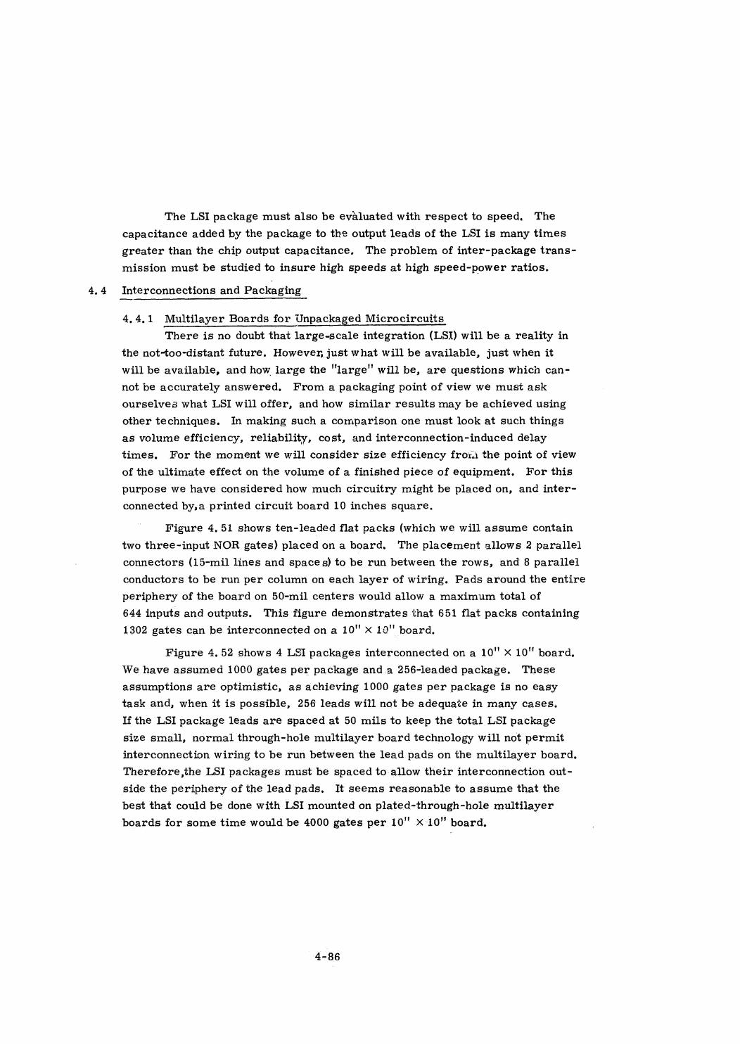
4.4
The LSI package must also be evaluated with respect to speed, The
capacitance added by the package to the output leads of the LSI is many times
greater than the chip output capacitance, The problem of inter-package trans-
mission must be studied to insure high speeds at high speed-powerratios.
Interconnections and Packaging
4,4,1 Multilayer Boards for Unpackaged Microcircuits
There is no doubt that large-scale integration (LSI) will be a reality in
the not-too-distant future. However,just what will be available, just when it
will be available, and how large the "large" will be, are questions which can-
not be accurately answered, From a packaging point of view we must ask
ourselves what LSI will offer, and how similar results may be achieved using
other techniques. In making such a comparison one must look at such things
as volumeefficiency, reliability, cost, and interconnection-induced delay
times, For the mament we will consider size efficiency froxi the point of view
of the ultimate effect on the volume of a finished piece of equipment. For this
purpose we have considered how much circuitry might be placed on, and inter-
connected by,a printed circuit board 10 inches square.
Figure 4,51 shows ten-leaded flat packs (which we will assume contain
two three-input NOR gates) placed on a board, The placement allows 2 parallel
connectors (15-mil lines and spaces) to be run between the rows, and 8 parallel
conductors to be run per column on e@ach layer of wiring. Pads around the entire
periphery of the board on 50-mil centers would allow a maximum total of
644 inputs and outputs. This figure demonstrates that 651 flat packs containing
1302 gates can be interconnected on a 10" X 10" board.
Figure 4,52 shows 4 LSI packages interconnected on a 10" X 10" board.
We have assumed 1000 gates per package and.a 256-leaded package. These
assumptions are optimistic, as achieving 1000 gatesper package is no easy
task and, when it is possible, 256 leads will not be adequate in many cases.
If the LSI package leads are spaced at 50 mils to keep the total LSI package
size small, normal through-hole multilayer board technology will not permit
interconnection wiring to be run between the lead pads on the multilayer board.
Therefore ,the LSI packages must be spaced to.allow their interconnection out~
side the periphery of the lead pads, It seems reasonable to assumethat the
best that could be done with LSI mounted on plated-through-hole multilayer
boards for some time would be 4000 gates per 10" x10" board.
4-86
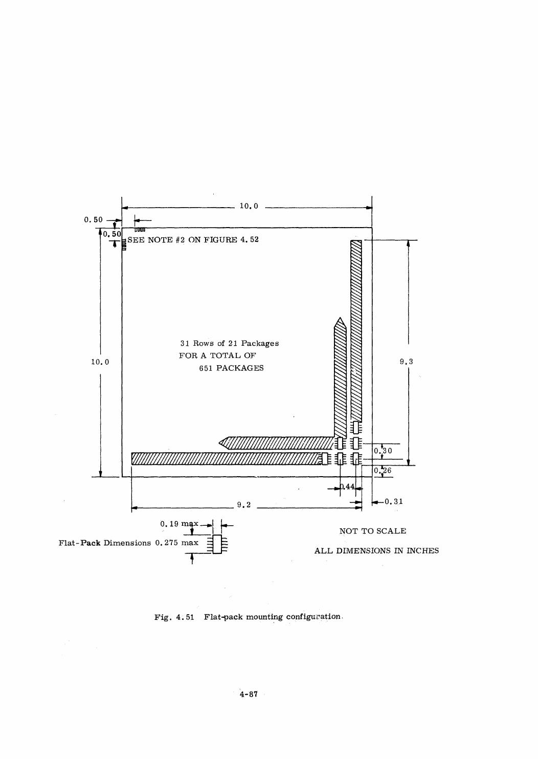
| 10.0 1
0.50 el
a80,504-gSEE NOTE #2 ON FIGURE 4.52
31 Rows of 21 Packages
FOR A TOTAL OF
10.0 651 PACKAGES oe
0.26
9.9 =-0.31
0,19 max —elLl fr NOT TO SCALE
Flat-Pack Dimensions 0.275 max
+ ALL DIMENSIONS IN INCHES
Fig. 4.51 Flat-pack mounting configuxation.
4-87
10,0 I
FUSER LATTEEEE LLPPEDDIPE +
PUPEPIEIIETT
TTVTTTTTTTTTETri
PELITELIEPED
TETTTTT
TTT
TTTTTeT
10,0 TOTTI TTT TIT TTT TTTTTT TTT TTT as
0,7(GUUURUOLUERRHERCRERERREEE, LLLLEL tereooo
2 E = L
= a E_ C = C
bs ee C
a — = om
4 - 7 r 3.83 bE 4 *SEE NOTE #1 b
4 = = LE
*SEE NOTE #2 > FO E |0.15 ¥ TUTTI TIT T TTT TTTTTT TT TIT TTTITIT TT TTT TTT TTT TT i
1 ore 0.85a Log— . J
otis ol be | | e7 3.8 IS. est—we e905
ALL DIMENSIONS IN INCHES
*NOTE #1 *NOTE #2
256 Leads Per Flat-Pack 161 Lead Pads Per Side
64 Leads Per Side Iuead Pads 0,05 Center-to-Center
Leads 0,05 Center-to-Center Lead Pads 0.035 Wide By 0.15 Long
Leads 0.15 Long
Fig. 4.52 LSI mountingconfiguration.
4-88

Ever since the advent of the transistor, people have pointedout the
terrific volume advantages tc be gained if the package could be eliminated.
This is also true for microcircuits and even true for LSI, For example (con-
sidering relative areas) a 2-gate NOR chip is about 40 mils square whereas
the flat pack and leads necessary to attach it into the circuit are about
275 X 400 mils or about 70 times as big. The ratio for LSI is not as bad,
but still not good,at something like 10:1, The inability to properly passivate
semiconductor surfaces and difficulties in handling of small chips seemedto
be the prime deterrents to this scheme for a long time. Good passivation is
now a reality. Chip handling is greatly improved. But,from a system point
of view,there is still the large deterrent of adequate handling and intereonnec-
tion of chips in large numbers on a wiring board of minute dimensions. The
present state of the art for multilayer circuit boards of ceramic or plastic is
about 5-mil lines and spaces, Using such a wiring board would allow dual-gate
chips to be placed on 100-mil centers, or 200 gates per square inch of board.
Just how many gates could be economically interconnected is dependent upon
several factors, some of which are listed below:
1 The quality of chips being attached,
2. The yield of the attachment process.
3. The abilityto remove chips a:d attach new ones.4 The factors involved in testing the completed circuit.
If we assumed for the sake of argument that we could fill the entire LSI
package (about 10 in? of usable area) with dual chips interconnected on 100-mii
centers, wefind we could get 2000 gates into it. Whether we would have enough
package leads would dependon the system design and partitioning. Of course,
handling so many chips using present te -hniques is impractical from a yield
point of view (as is LSI), If we scale ¢ + goal down to 1- or 2-hundred chips
per package, the system packing density is still attractive, and the technology
to achieve it is close at hand.
The packing density achieved using a scheme of interconnecting un-
packaged circuits offers other potential advantages of LSI, such as shorter
propagation delays becauseof shorter paths, lower cost because the numberof
hermetic packages,is greatly reduced, and increased reliability because the
number of bonds made is reduced. It also is a versatile scheme and,therefore,
attractive for a small numberof networks. .
. Development efforts in interconnecting unpackageddevices and circuits
wiil be oflasting value because, as medium-scale and large-scale integration
evolves, the same techniques developed for interconnection using high-density.
4-89
multilayer boards can be used to interconnect the larger scales of integration.
We believe this effort should be stimulated in view of its long-term future
potential. .Tc this end we have started an investigation into the use of multi-
layer boards for this purpose. The short-term goal of this investigation is to
interconnect about 200 gates into an arithmetic unit in a hermetic flat pack
about 1.5 inches square,
4,4,2 System Packaging and Interconnections
The designer of a large computer package suitable for goace system use
must simultaneously take into consideration electrical interconnections, mech-
anical integrity and heat transfer. Failure to consider these items and their
interrelations as a whole will result in an inferior design.
Interconnections have required a larger proportion of system volume as
components have been reduced in size, Connectors and intermodule wiring
panels account for about 60% of the total volume on the Apollo Guidance Com-
pute>. Printed circuit boards offer a volume advantage over wire-wrap panels
and advantage should be taken of this technology where possible. Another reason
for considering the useof printed circuit board over wire-wrap panels is that
one may be tempted to make wiring changes on existing wire-wrap panels and in
the process possibly decrease their reliability. This temptation does not exist
with printed circuit boards.
There are at least three ways to reduce connector volume in a system.
The first, and most important, is to design out as many connectors as possible.
This can be done by thoughtful partitioning of the system and by making the
partitional sections as large as possible consistent with test and repair pro-
blems. There may be times when oneis limited in section-size design because
the area available for making connections decreases, in ratio to the volume,
as the section increases in size. This problem can be alleviated if one designs
a connection system capable of making connections on more than one surface
or edge of the section. A second way is to miniaturize the connector as much
as possible. Of course there are limits as to how far such miniaturization can
be carried without jeopardizing the connector reliability. A third way to reduce
connector volume is to make parts of the system package serve also as parts of
the connector. Before attempting this, it is worthwhile to ask just what a con-
nectoris,
A connector is basically two mating surfaces and a systemfor making
and maintaining their contact. (For purposesof design it is instructive to note
that almost all the connector volume is devoted to maintaining surface contact,
4-90
a miniscuie amount is devoted to mating surfaces), The requirement for a
mating force makes plugging and unplugging connectors with many contacts
so difficult that jacking screws are often required. These screws might be
eliminated if the plugging force could be applied by other existing members
of the computer package. ,
Connector failure occurs if the mating surfaces are rendered non-con-
ductive, or if contact breaks. Properly-designed connectors are quite reliable;
however, if a large increase in reliability is required, redundant connections
should be seriously considered,
Present system-design concepts call for some high-frequency connections
between different machines in the system, such as between processors. These
connections will probably require the use of a strip line or something com-
parable. Our prototype package design accounts for this possibility by allowing
adequate connector area for this purpose.
The heat transfer paths though connectors and structural members should
be considered as a whole in the design stage. If the connectors can be arranged to
transfer heat as well as electricity without undue design compromise, a definite
advantage can be gained. In addition, if the structure of the connector is used also
as part of the package structure, or from the opposite point of view if the package
structure is used as part of the connector, an advantage is gained.
Of course, the structural membersof the system package must be designed’
and arranged to withstand mechanical stresses such as shock and vibration.
In addition, since the structural members are usually made from excellent
thermal conductors such 4s aluminum or magnesium, they should be designed
to provide adequate thermal paths from areas of heat generation to the surface
of the system. This requires that the thermal resistance from all heat genera-
tors to structural members be small, and that the thermal path through the
structural memberto the cooling surfaces be short and unimpeded by structural
joints with high thermal impedance. One possibility is a design where all main
structural members extend to four sides of the system package. They could
then easily be connected to cold rails of radiators on one or more sides as
necessary.
On the basis of the\preceding,a prototype model for the structure of a
processor was designed and is being built. The design consists simply of four
plates 10" x 10" x 1/8" which have 8 raised pillars around the periphery to
space the plates. Bolts through the pillars hold the stack together. Each plate
4-91
provides a mechanical support and heat+transfer path for circuitry mounted
on it, Printed circuit boards can be attached to both sides of the plates (ex-
cept the top and bottom plates). Connections between the boards (all four
edges) are provided by special connectors. These connectors are not plugged
in; they are stacked between the plates and compressed when the assembly
is bolted together. In addition, a connector is provided on one side of the
assembly to connect the processor into the system. On the same side,
tapped holes are provided in the pillars to bolt the assembly against cold
rails for cooling.
This packaging scheme is simple and yet versatile, Such things as
rope memories, discrete component assemblies, etc., can be potted in, or
stacked on a plate (which of course can varyin thickness and in spacing to
the next plate), The connector takes up a relatively small part of the volume.
Simple heat-transfer paths wiil make thermal computations simple, and the
results cool.
4.4.3 Soft Metal Connector Contacts
High-density (,050''-center or less) connectors for the interconnection
of printed wiring boards are necessary for improved airborne-systems
packaging, Because prior experiments using spectrographic analysis techniques
indicated that indium in high-pressure contact with nickel diffuses across the
surface contact, one approach might make use of this mechanism to create
low-resistivity contacts. |
The vehicle used to test this concept consisted of sets of flat 25-mil-
wide indium-plated fingers placed on 50-mil centers between nickel printed
circuit boards with corresponding pad areas on the boards. A piece of
elastomer waslaid over one of the boards ard the assembly was put under
pressure with metal plates pulled together with screws. Similar assemblies
were made using gold-plated fingers and pad areas for comparison. The
fingers were considered expendable, and new ones were used everytime con-
nection was broked.
Storage tests of the indium-nickel system for over 10,000 hours at
room temperature indicate a slight increase in resistance probablydue to the
elastomer taking a permanent set and thereby reducing contact pressure.
There was no evidence of alloying, which is attributed to too-low contact
.,pressure, Connectors were mounted and demounted morethan 100times with-
| out excessive damage. The gold-gold system had lower initial resistance
than the indium-nickel system and it has remained lower for the duration of
the test, Tentative conclusions are that unless contact pressure can be in-
creased and/or elevated tempevature is applied to the connectorto start the.
process, diffusion will not occur, and the expected advantage of the system |
will not be realized,
4-92
5. CONCLUSIONS AND RECOMMENDATIONS
D1 The Role of Computer Research and Development
The ACGN System, and indeed many, if not all, exploratory spacecraft
systems for the coming decade,wili have data processing requirements beyond the
reach of hardware available today for reasons of size, power consumption, per-
formance, and/or reliability. The forthcoming technology offers the possibility
not only of making improvements with respect to all of these characteristics, but
of doing it in such a way as to trade one off against another within the same family
of computers.
We have shown that a multiprocessor structure is feasible for an important
class of applications, and provides an unprecedented measure of flexibility in
adaptations to specific missions by means of its capacity to expand and contract.
Processors, memories, 1/0 Buffers, and in fact programs are items which can
carry over from one system to another, large or small,
The spaceborne multiprocessor is as yet an untried and untested machine.
Numerous workers have proposed various embodimentsof the basic modular
notion, none of which has been realized. Ground-based multiprocessors have
been built, however, and are operational in both data processing and control
environments. The difficult part of developing the spaceborne multiprocessor lies
in making it capable of transient and permanent fault recovery in a way that is trans-
parent to the mission programmer. This can surely be done, though not without
substantial effort. The rewards in terms of potential spacecraft system per-
formance, commonality, and reliability are so great, however, as to amply
justify the effort.
A combined hardware and software development is needed to realize the
multiprocessor which we.propose. Elements of this development effort include
simulations of the structure, prototype fabrication, advanced hardware design,
and programming. These elements are taken up in the following sections.
5 2 Simulations
Thefirst task in continued development of the multiprocessor is to model
the proposed system and exercise it to find its weaknesses. Using ‘data-processing
facilities available through MIT's OLLS (On-Line Logical Simulation) effort, a
computer~aided computer design progi‘am, it will be possible to test suchvital
functionsas the executive structure, bus traffic statistics, program execution .
statistics, and error control techniques.
As the design is further refined, it is proposed that the individual
subunits of the multiprocessor, such as processors, memories, and the I/0_
Buffer, be modeled separately on small digital computers, which can be inter-
connectedvia a bus to moreclosely resemble the proposed system. Not only would _
5-1
this allow a more detailed study than OLLS would efficiently furnish, but it
would allow prototype hardwareto be exercised by direct replacementof its digital
computer model.
5.3 Prototype Fabrication
In addition to the software simulations just described, hardware simulations
are also required before the design can be completed. Most notable in this
regard is the bus system which not only is new and untried, but which is also a
requirement for the individual unit simulation scheme of the preceding paragraph.
Other facets of the system which require preliminary exploration in hardware form are
hardware error control, memory paging circuits, arithmetic unit, sequence
generators, and numerous other aspects of logical/electrical design.
Prototype fabrication would preferably begin right away at a low level, and
increase later on when subunit designs begin to be made in detail. Fast turn-
around is desired so that hardware can be exercised and redesigned as necessary.
Computer-aided design enhances the turn-around speed, as do such techniques
as wire wrapping, which may in some cases be used in preference to more ad-
vanced but less expeditious interconnection techniques such as multilayer boards.
As designs advance in their maturity, prototype efforts must more closely resemble
the final configuration.
All final designs, of course, need to be proven in prototype form before they
can be committed to production. Because of the particularly long-turn. - around
times experienced on production lines, an in-house capability to produce final-
configuration hardware on a small scale would greatly enhance design verification
and early production quality. Experience with Apollo indicates that a greater
investment in prototype facilities would have been more than repaid in reduction
of retrofit costs.
5.4 Advanced Circuit Development
Substantial progress in semiconductors and their intereonnection is desired
for the advanced computer in order to realize high speed, small size, and low power
consumption along with high reliability. These aretraditionally very long lead-
“time matters, and the irsportance of an early start is clear.
The effort should consist of continued scrutiny of the semiconductor market
plus the experimental implementation of interconnections using newly developed
thin- and thick-film deposition techniques, applied to small-, medium-, and .
large-scale integrated circuits alike. This effort will merge with the prototype
fabrications at the earliest possible time. |
Memory research is another aspect of advanced circuit development.
Braid, plated wire, ferrite core, tape, and semiconductor scratchpad memory
development are all indicated. Much of this development is already being carried
on, both here and elsewhere, independent of the multiprocessor design. The Braid
memory is more nearly unique to MIT/IL, and, since it is a prime candidate for
both sequence generators and program memories, merits a certain degree of
emphasis.
5.5 Software Development
The design of a software system for a multiprocessor computer is a
challenge which has not yet been broadly met. The programming conventions
required and means for their implementation have been described to a limited
extent elsewhere in this report. It is apparent that attempting to implement
programming conventions in the hardware (storage protection, restart
protection, etc.) would be expensive and, further, would not be readily subject
to modification should deficiencies in the design appear later than in theinitial
development stages. The most attractive solution to the convention-enforcement
problem is the use of a sophisticated compiler, whose input language is one which
permits the programmerto express his program in a form least subject to error.
The conversion of this input language to code for the multiprocessor would be
designed so that programming conventions would be automatically applied. In this
way, the possibility of errors and violation of conventions would be minimized,
while the flexibility of having the rules implemented in software would be achieved.
Thus, the development of a suitable language and compiler represents the |
major software support task. Even though this approach tends to reduce the
number of opportunities for error in the preparation of mission programs,
development effort will also be required to design and write programsto aid in
mission program checkout. Initiation of design effort in these areas could
occur in parallel with the completion of the formulation of program conventions
and solidification of those aspects of logical design of the hardware which
fundamentally affect the software, such as word size, page size, instruction
repertoire, addressing method, etc. |
5-3
Related Documents