A High Power H-Bridge Vincent Sieben September 2003 - Revision 1.0

Hbridge Reference Ualberta Arvp
Dec 29, 2015
Welcome message from author
This document is posted to help you gain knowledge. Please leave a comment to let me know what you think about it! Share it to your friends and learn new things together.
Transcript

A High Power H-Bridge
Vincent Sieben
September 2003 - Revision 1.0
Contents
1 Overview 1
1.1 Brief Specifications of High Power H-Bridge . . . . . . . . . . . . . . . . 1
2 H-Bridge Principles 2
2.1 Direction Control - H-Bridge Topology . . . . . . . . . . . . . . . . . . . 2
2.2 Speed Control - PWM Technique . . . . . . . . . . . . . . . . . . . . . . 5
3 Design Description 7
3.1 Turning On The Upper MOSFETS . . . . . . . . . . . . . . . . . . . . . 7
3.1.1 MOSFET Driver Chip - HIP4081A . . . . . . . . . . . . . . . . . 7
3.2 Feedback EMF Reduction - Large Main Capacitor . . . . . . . . . . . . 9
3.3 Regenerative Current Circulation . . . . . . . . . . . . . . . . . . . . . . 9
3.4 Shoot-Through Protection . . . . . . . . . . . . . . . . . . . . . . . . . . 12
4 Pictures of Final PCB 13
5 Future Improvements 14
Bibliography 15
A Final Schematic 16
B Final PCB 18
C Bill of Material - BOM 22
Chapter 1
Overview
This document is intended to give an introduction to H-Bridges and to briefly ex-
plain the design principles behind the schematic diagram of the High Power H-Bridge
designed. The reader is encouraged to look over the reference list at the end of the
document for further information on H-Bridges and Power electronics.
1.1 Brief Specifications of High Power H-Bridge
• 70 Amps - Continuous Current
• 150 Amps - Maximum Current (Short Durations)
• 48 Volts - Maximum Voltage
• 200 mA - Standby By current
• Direction and PWM as inputs
• Solid State - Fast Directional Changing
ARVP - Autonomous Robotic Vehicle Project Page 1
Chapter 2
H-Bridge Principles
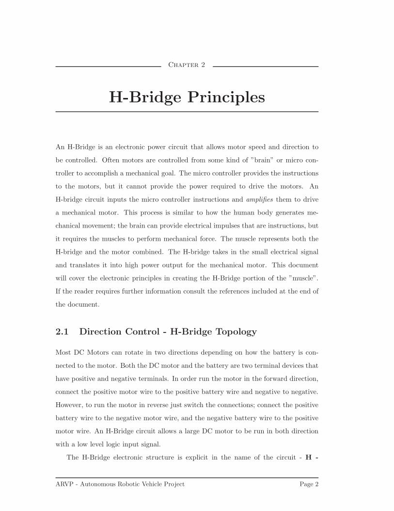
An H-Bridge is an electronic power circuit that allows motor speed and direction to
be controlled. Often motors are controlled from some kind of ”brain” or micro con-
troller to accomplish a mechanical goal. The micro controller provides the instructions
to the motors, but it cannot provide the power required to drive the motors. An
H-bridge circuit inputs the micro controller instructions and amplifies them to drive
a mechanical motor. This process is similar to how the human body generates me-
chanical movement; the brain can provide electrical impulses that are instructions, but
it requires the muscles to perform mechanical force. The muscle represents both the
H-bridge and the motor combined. The H-bridge takes in the small electrical signal
and translates it into high power output for the mechanical motor. This document
will cover the electronic principles in creating the H-Bridge portion of the ”muscle”.
If the reader requires further information consult the references included at the end of
the document.
2.1 Direction Control - H-Bridge Topology
Most DC Motors can rotate in two directions depending on how the battery is con-
nected to the motor. Both the DC motor and the battery are two terminal devices that
have positive and negative terminals. In order run the motor in the forward direction,
connect the positive motor wire to the positive battery wire and negative to negative.
However, to run the motor in reverse just switch the connections; connect the positive
battery wire to the negative motor wire, and the negative battery wire to the positive
motor wire. An H-Bridge circuit allows a large DC motor to be run in both direction
with a low level logic input signal.
The H-Bridge electronic structure is explicit in the name of the circuit - H -
ARVP - Autonomous Robotic Vehicle Project Page 2
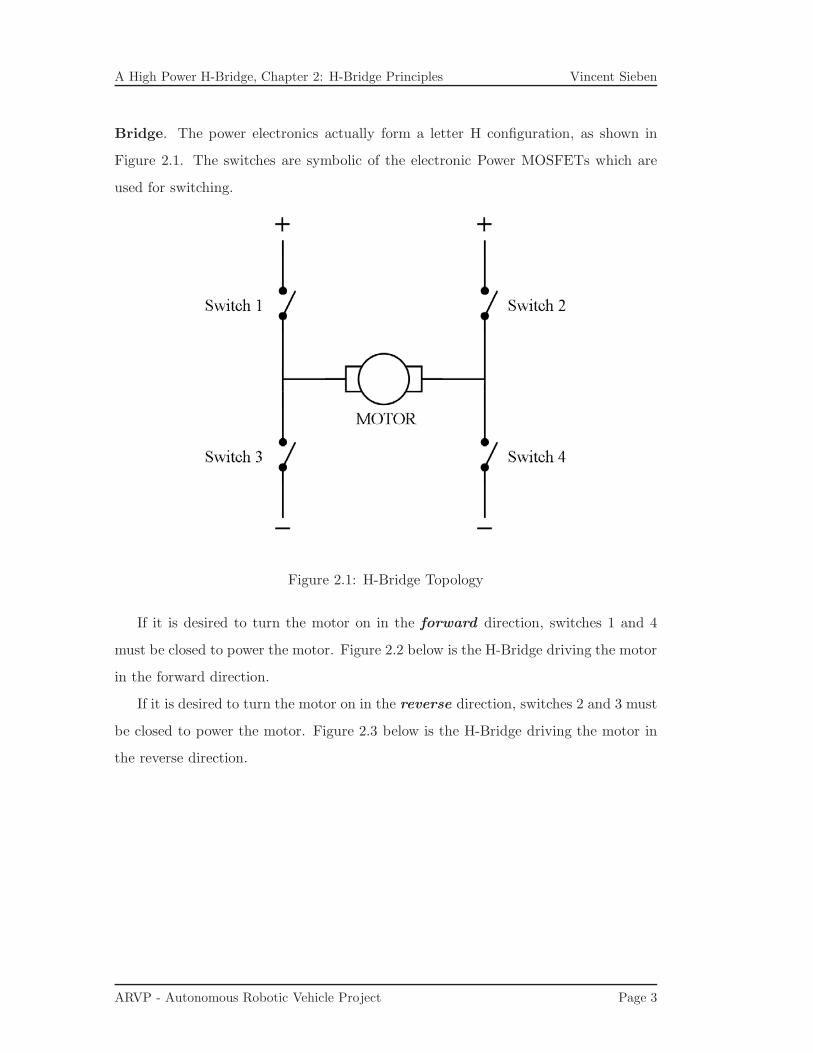
A High Power H-Bridge, Chapter 2: H-Bridge Principles Vincent Sieben
Bridge. The power electronics actually form a letter H configuration, as shown in
Figure 2.1. The switches are symbolic of the electronic Power MOSFETs which are
used for switching.
Figure 2.1: H-Bridge Topology
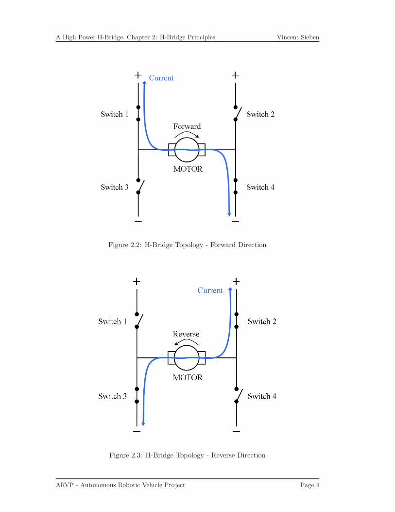
If it is desired to turn the motor on in the forward direction, switches 1 and 4
must be closed to power the motor. Figure 2.2 below is the H-Bridge driving the motor
in the forward direction.
If it is desired to turn the motor on in the reverse direction, switches 2 and 3 must
be closed to power the motor. Figure 2.3 below is the H-Bridge driving the motor in
the reverse direction.
ARVP - Autonomous Robotic Vehicle Project Page 3
A High Power H-Bridge, Chapter 2: H-Bridge Principles Vincent Sieben
Figure 2.2: H-Bridge Topology - Forward Direction
Figure 2.3: H-Bridge Topology - Reverse Direction
ARVP - Autonomous Robotic Vehicle Project Page 4
A High Power H-Bridge, Chapter 2: H-Bridge Principles Vincent Sieben
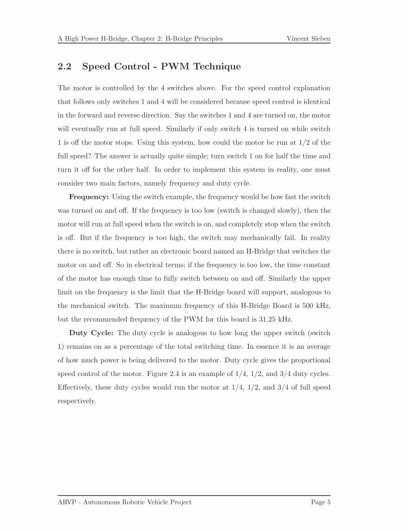
2.2 Speed Control - PWM Technique
The motor is controlled by the 4 switches above. For the speed control explanation
that follows only switches 1 and 4 will be considered because speed control is identical
in the forward and reverse direction. Say the switches 1 and 4 are turned on, the motor
will eventually run at full speed. Similarly if only switch 4 is turned on while switch
1 is off the motor stops. Using this system, how could the motor be run at 1/2 of the
full speed? The answer is actually quite simple; turn switch 1 on for half the time and
turn it off for the other half. In order to implement this system in reality, one must
consider two main factors, namely frequency and duty cycle.
Frequency: Using the switch example, the frequency would be how fast the switch
was turned on and off. If the frequency is too low (switch is changed slowly), then the
motor will run at full speed when the switch is on, and completely stop when the switch
is off. But if the frequency is too high, the switch may mechanically fail. In reality
there is no switch, but rather an electronic board named an H-Bridge that switches the
motor on and off. So in electrical terms; if the frequency is too low, the time constant
of the motor has enough time to fully switch between on and off. Similarly the upper
limit on the frequency is the limit that the H-Bridge board will support, analogous to
the mechanical switch. The maximum frequency of this H-Bridge Board is 500 kHz,
but the recommended frequency of the PWM for this board is 31.25 kHz.
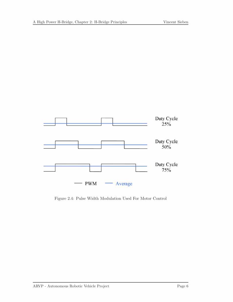
Duty Cycle: The duty cycle is analogous to how long the upper switch (switch
1) remains on as a percentage of the total switching time. In essence it is an average
of how much power is being delivered to the motor. Duty cycle gives the proportional
speed control of the motor. Figure 2.4 is an example of 1/4, 1/2, and 3/4 duty cycles.
Effectively, these duty cycles would run the motor at 1/4, 1/2, and 3/4 of full speed
respectively.
ARVP - Autonomous Robotic Vehicle Project Page 5
A High Power H-Bridge, Chapter 2: H-Bridge Principles Vincent Sieben
Figure 2.4: Pulse Width Modulation Used For Motor Control
ARVP - Autonomous Robotic Vehicle Project Page 6
Chapter 3
Design Description
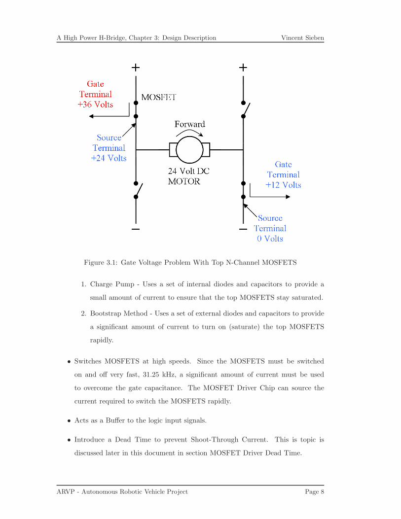
3.1 Turning On The Upper MOSFETS
This section will explain what the ”switches” above actually are in terms of electronic
components. The switches are power MOSFETs (transistors) that have certain proper-
ties that allow them to switch high currents based on an input signal. The MOSFETs
are used in two regions of operation; Cut-off mode and Saturation mode which cor-
respond to switched off and switched on respectively. In the H-Bridge case, to put
a MOSFET into the Cut-off mode, the input signal (Gate Voltage) to the MOSFET
must be grounded. However, to turn on the MOSFETs and put them into saturation
mode requires a more complicated process.
MOSFETS are three terminal devices with the terminals being the Gate, Drain,
and Source. In order to turn on the MOSFET into saturation mode the voltage at
the gate terminal must be approximately 12 volts higher than the voltage at source
terminal. Figure 3.1 illustrates the slightly more complicated process of turning on
the top MOSFETS.
The more complicated part; how can 36 volts be used at the Gate when the battery
voltage is only 24V? The MOSFET Driver chip solves this problem by using a Charge
Pump and a Bootstrap circuit.
3.1.1 MOSFET Driver Chip - HIP4081A
A MOSFET driver chip performs all of the following functions.
• Generate the VGS to turn on (saturate) the top N-Channel MOSFETS. This is
accomplished by two methods, a charge pump and a bootstrap circuit. Informa-
tion on both these methods can be found in data sheet for the HIP4081A, or in
the references at the end of this document.
ARVP - Autonomous Robotic Vehicle Project Page 7
A High Power H-Bridge, Chapter 3: Design Description Vincent Sieben
Figure 3.1: Gate Voltage Problem With Top N-Channel MOSFETS
1. Charge Pump - Uses a set of internal diodes and capacitors to provide a
small amount of current to ensure that the top MOSFETS stay saturated.
2. Bootstrap Method - Uses a set of external diodes and capacitors to provide
a significant amount of current to turn on (saturate) the top MOSFETS
rapidly.
• Switches MOSFETS at high speeds. Since the MOSFETS must be switched
on and off very fast, 31.25 kHz, a significant amount of current must be used
to overcome the gate capacitance. The MOSFET Driver Chip can source the
current required to switch the MOSFETS rapidly.
• Acts as a Buffer to the logic input signals.
• Introduce a Dead Time to prevent Shoot-Through Current. This is topic is
discussed later in this document in section MOSFET Driver Dead Time.
ARVP - Autonomous Robotic Vehicle Project Page 8
A High Power H-Bridge, Chapter 3: Design Description Vincent Sieben
3.2 Feedback EMF Reduction - Large Main Capacitor
The large main capacitors primary purpose is to suppresses transient spikes caused
by the motor. Often when the motor accelerates, decelerates, or stops suddenly, an
EMF ”feedback” voltage will spike on the main battery voltage. These spikes cause
micro controllers to reset and are harmful to most low level electronics. By placing a
filter capacitor in parallel with the battery, these feedback spikes can be reduced in
magnitude.
The reasoning behind this filter capacitor has its roots in basic electronics. One
of the laws from basic electronics states that voltage can not change instantaneously
across a capacitor; therefore, since the capacitor is parallel to the battery, the battery
voltage cannot change instantly. This results in a reduction of the feedback voltage
spikes generated by the motor.
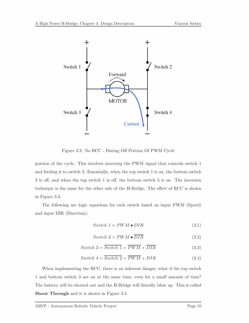
3.3 Regenerative Current Circulation
Another law from basic electronics states that current cannot change instantaneously
through an inductor. Since the main motor coil is a large inductor, the current running
through the motor can only change gradually. Abrupt changes cause the feedback
voltage spikes mentioned earlier. As an additional feature to the main capacitor,
an RCC (regenerative current circulation) technique was implemented to reduce EMF
voltage spikes. Additionally, the RCC technique implemented redirects unused current
back into the battery, maximizing battery life.
Recall that when using the PWM technique, the upper switch is rapidly turned
on and off to create variable speed control, and the lower switch is left on. When
the motor is running at 1/2 speed, the top switch (switch 1) is switched on 1/2 the
time and it is switched off 1/2 the time. During the OFF part of the PWM cycle
(switch 1 - off and switch 4 - on), where does the current circulate? Remember this is
a large inductor and current cannot jump from a definite value to zero instantly!, see
Figure 3.2.
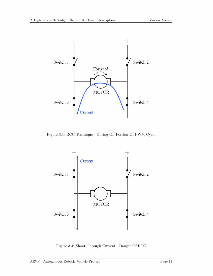
To solve this problem, the PWM technique will be refined to incorporate RCC. The
RCC technique involves turning on both bottom switches when the PWM is in the off
ARVP - Autonomous Robotic Vehicle Project Page 9
A High Power H-Bridge, Chapter 3: Design Description Vincent Sieben
Figure 3.2: No RCC - During Off Portion Of PWM Cycle
portion of the cycle. This involves inverting the PWM signal that controls switch 1
and feeding it to switch 3. Essentially, when the top switch 1 is on, the bottom switch
3 is off, and when the top switch 1 is off, the bottom switch 3 is on. The inversion
technique is the same for the other side of the H-Bridge. The effect of RCC is shown
in Figure 3.3.
The following are logic equations for each switch based on input PWM (Speed)
and input DIR (Direction):
Switch 1 = PWM • DIR (3.1)
Switch 2 = PWM • DIR (3.2)
Switch 3 = Switch 1 = PWM + DIR (3.3)
Switch 4 = Switch 2 = PWM + DIR (3.4)
When implementing the RCC, there is an inherent danger; what if the top switch
1 and bottom switch 3 are on at the same time, even for a small amount of time?
The battery will be shorted out and the H-Bridge will literally blow up. This is called
Shoot Through and it is shown in Figure 3.4.
ARVP - Autonomous Robotic Vehicle Project Page 10
A High Power H-Bridge, Chapter 3: Design Description Vincent Sieben
Figure 3.3: RCC Technique - During Off Portion Of PWM Cycle
Figure 3.4: Shoot Through Current - Danger Of RCC
ARVP - Autonomous Robotic Vehicle Project Page 11
A High Power H-Bridge, Chapter 3: Design Description Vincent Sieben
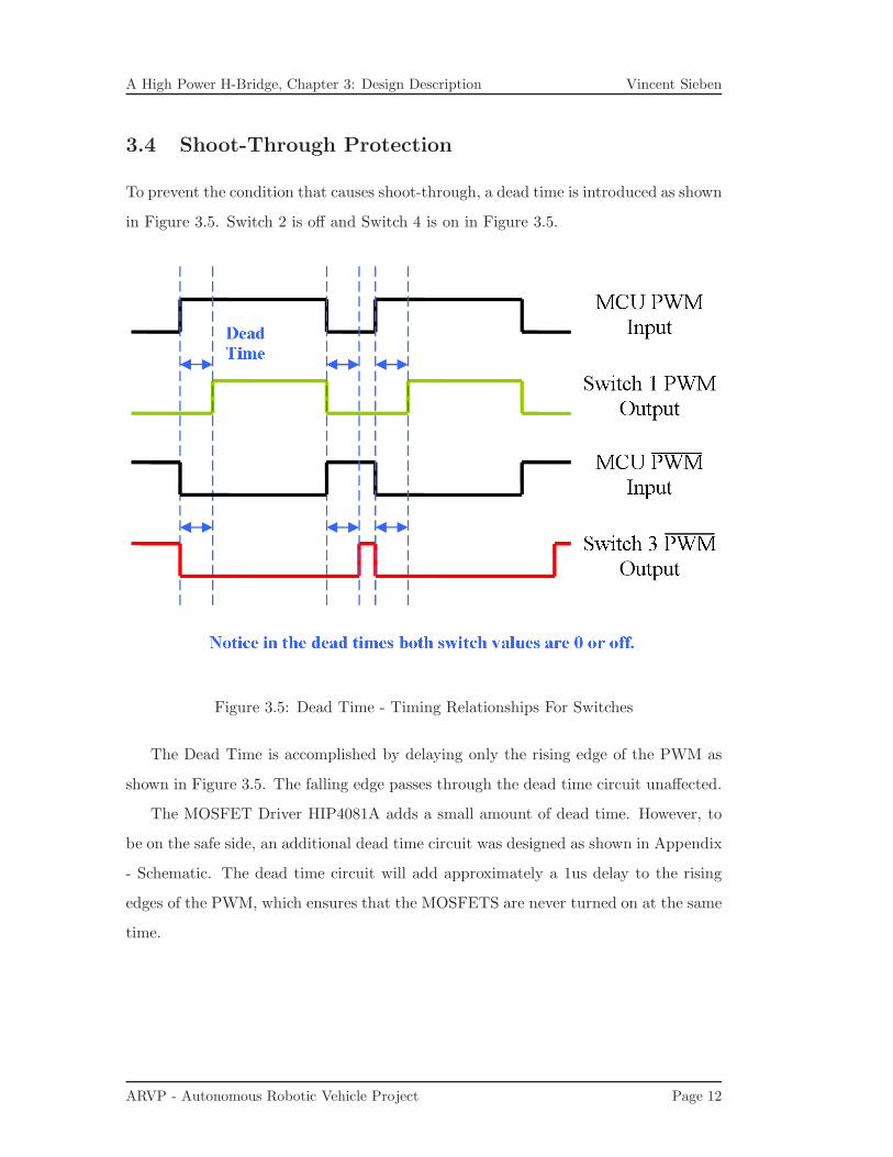
3.4 Shoot-Through Protection
To prevent the condition that causes shoot-through, a dead time is introduced as shown
in Figure 3.5. Switch 2 is off and Switch 4 is on in Figure 3.5.
Figure 3.5: Dead Time - Timing Relationships For Switches
The Dead Time is accomplished by delaying only the rising edge of the PWM as
shown in Figure 3.5. The falling edge passes through the dead time circuit unaffected.
The MOSFET Driver HIP4081A adds a small amount of dead time. However, to
be on the safe side, an additional dead time circuit was designed as shown in Appendix
- Schematic. The dead time circuit will add approximately a 1us delay to the rising
edges of the PWM, which ensures that the MOSFETS are never turned on at the same
time.
ARVP - Autonomous Robotic Vehicle Project Page 12
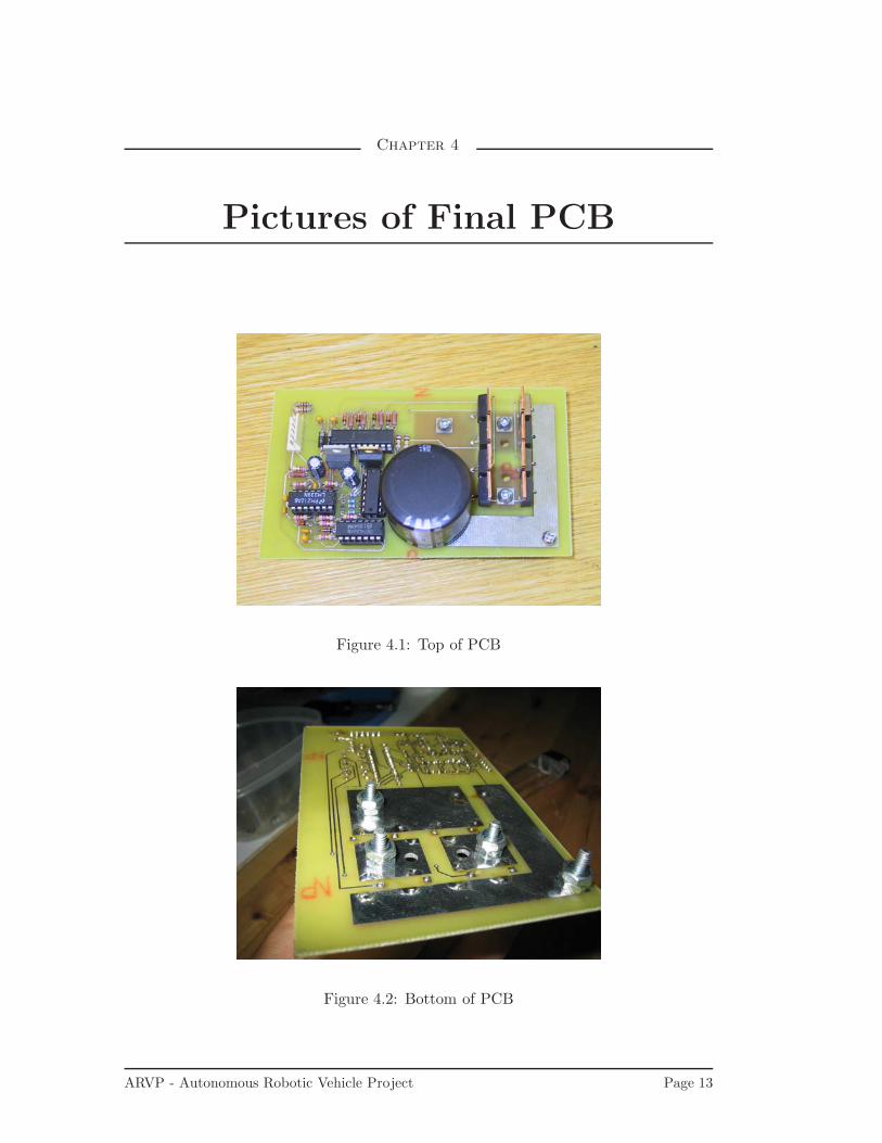
Chapter 4
Pictures of Final PCB
Figure 4.1: Top of PCB
Figure 4.2: Bottom of PCB
ARVP - Autonomous Robotic Vehicle Project Page 13

Chapter 5
Future Improvements
• Reduce PCB Size. Possibly incorporate two H-bridges on one board with a micro
controller.
• Switch the bottom MOSFETS instead of top MOSFETS.
• Possibly eliminate the voltage regulators and use Zener diodes instead.
ARVP - Autonomous Robotic Vehicle Project Page 14

Bibliography
[1] 4QD. Ncc70 reference manual. Technical report. URL: http://www.4qd.co.uk/.
[2] Intersil. Hip4081a data sheet. Technical report. URL:
http://www.intersil.com/.
[3] International Rectifier. Power mosfet application notes and data sheets. Technical
report. URL: http://www.irf.com/.
ARVP - Autonomous Robotic Vehicle Project Page 15

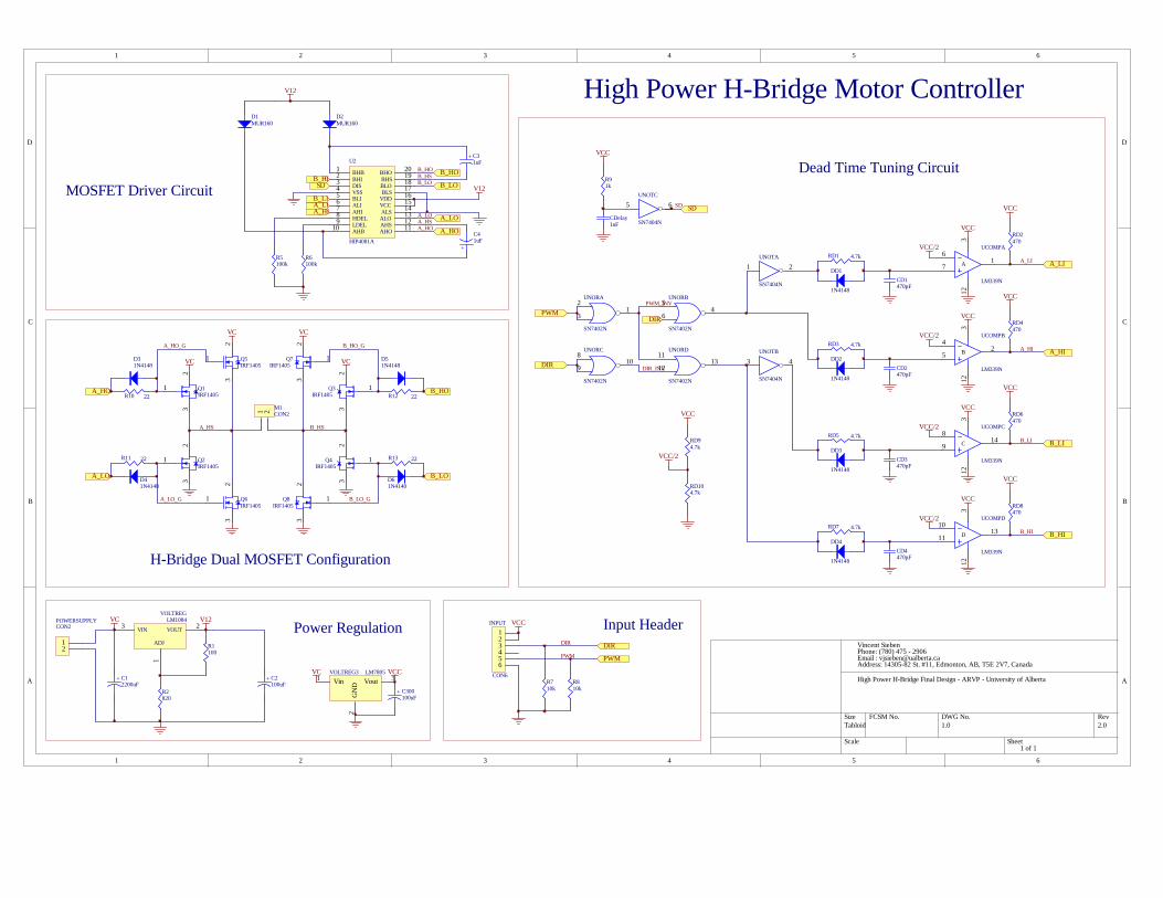
Appendix A
Final Schematic
ARVP - Autonomous Robotic Vehicle Project Page 16
1 2 3 4 5 6
A
B
C
D
654321
D
C
B
A
Scale Sheet
Size FCSM No. DWG No. Rev
1 of 1
Tabloid 1.0 2.0
Vincent SiebenPhone: (780) 475 - 2906Email : [email protected]: 14305-82 St. #11, Edmonton, AB, T5E 2V7, Canada
High Power H-Bridge Final Design - ARVP - University of Alberta
VC V12
+ C12200uF
+ C2100uF
12
POWERSUPPLYCON2 VIN VOUT
ADJ
23
1
VOLTREGLM1084
R1100
R2820
2
1
3
Q1IRF1405
2
1
3
Q2IRF1405
2
1
3
Q3IRF1405
2
1
3
Q4IRF1405
VC VC
1 2
M1CON2
D31N4148
R10 22
D41N4148
R11 22
D51N4148
R12 22
D61N4148
R13 22
A_HS B_HS
PWM
SD
R91k
VCC
R810k
R710k
123456
INPUT
CON6
DIR
VCC
DIR
PWM
DIR
PWM_INV
DIR_INV
PWM
DIR
SD
A_LI
B_LI
BHBBHIDISVSSBLIALIAHIHDELLDELAHB
BHOBHS
BLSVDDVCCALSALOAHS
123456789
10
2019
17161514
1213
AHO 11
BLO18
U2
HIP4081A
D2MUR160
V12
+ C31uF
V12
R6100k
R5100k
D1MUR160
+
C41uF
SD
A_LIB_LI
B_HO
B_LO
A_LO
A_HO
B_HO
B_LO
A_LO
A_HOA_HS
B_HS
B_HO
B_LOA_LO
A_HO
B_HI
A_HI
2
31
UNORA
SN7402N
5
64
UNORB
SN7402N
8
910
UNORC
SN7402N
11
1213
UNORD
SN7402N
1 2
UNOTA
SN7404N
3 4
UNOTB
SN7404N
DD1
1N4148
RD1 4.7k
CD1470pF
7
61
123
A
UCOMPA
LM339N
RD2470
VCC
VCC
VCC/2
DD2
1N4148
RD3 4.7k
CD2470pF
5
42
312
B
UCOMPB
LM339N
RD4470
VCC
VCC
VCC/2
DD3
1N4148
RD5 4.7k
CD3470pF
9
814
123
C
UCOMPC
LM339N
RD6470
VCC
VCC
VCC/2
DD4
1N4148
RD7 4.7k
CD4470pF
11
1013
312
D
UCOMPD
LM339N
RD8470
VCC
VCC
VCC/2
VCC
VCC/2
RD94.7k
RD104.7k
2
1
3
Q5IRF1405
VC
2
1
3
Q7IRF1405
VC
2
1
3
Q6IRF1405
2
1
3
Q8IRF1405
VC VCCVin1
GN
D2
Vout 3VOLTREG3 LM7805
+ C300100uF
A_HI
B_HI
A_LI
A_HI
B_LI
B_HI
5 6
UNOTC
SN7404NCDelay1uF
A_HO_G
A_LO_G B_LO_G
B_HO_G
High Power H-Bridge Motor Controller
Dead Time Tuning Circuit
MOSFET Driver Circuit
H-Bridge Dual MOSFET Configuration
Power Regulation Input Header

Appendix B
Final PCB
ARVP - Autonomous Robotic Vehicle Project Page 18
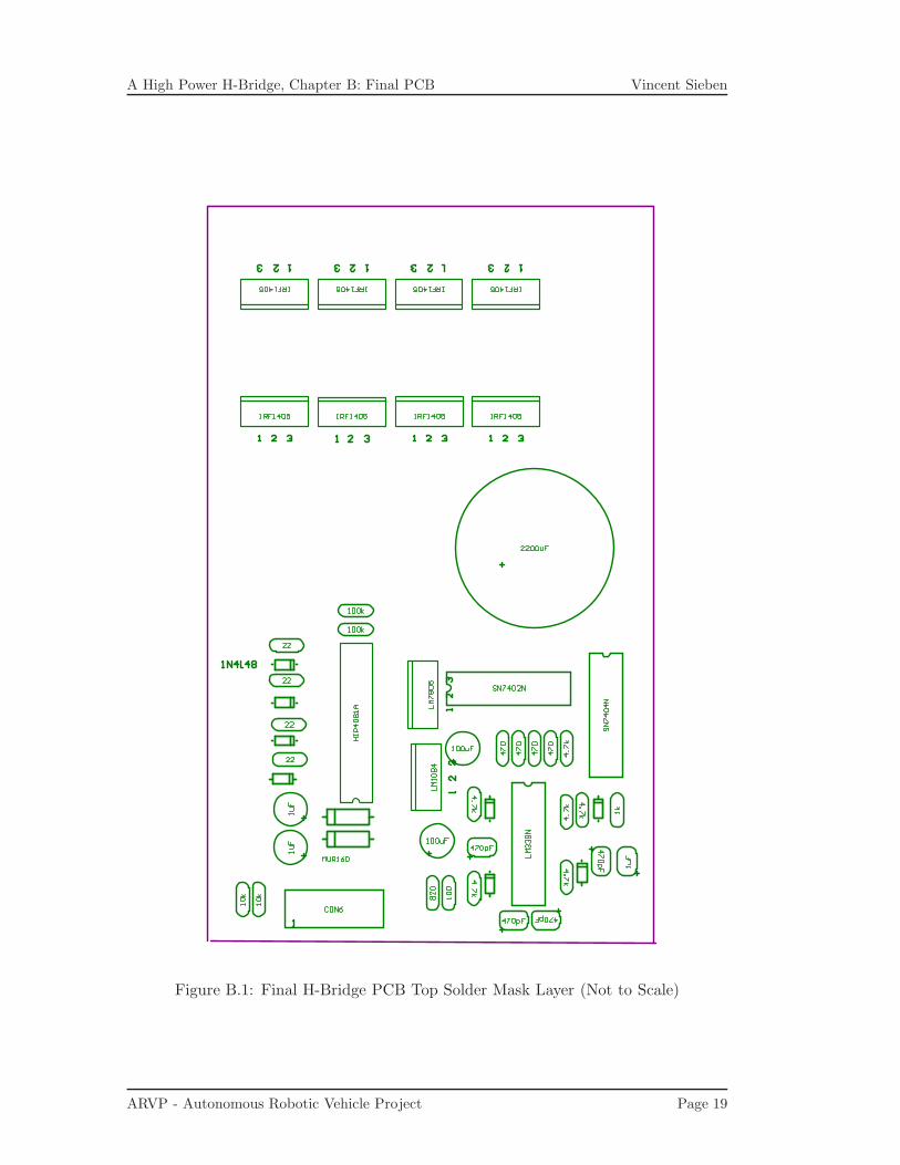
A High Power H-Bridge, Chapter B: Final PCB Vincent Sieben
Figure B.1: Final H-Bridge PCB Top Solder Mask Layer (Not to Scale)
ARVP - Autonomous Robotic Vehicle Project Page 19
A High Power H-Bridge, Chapter B: Final PCB Vincent Sieben
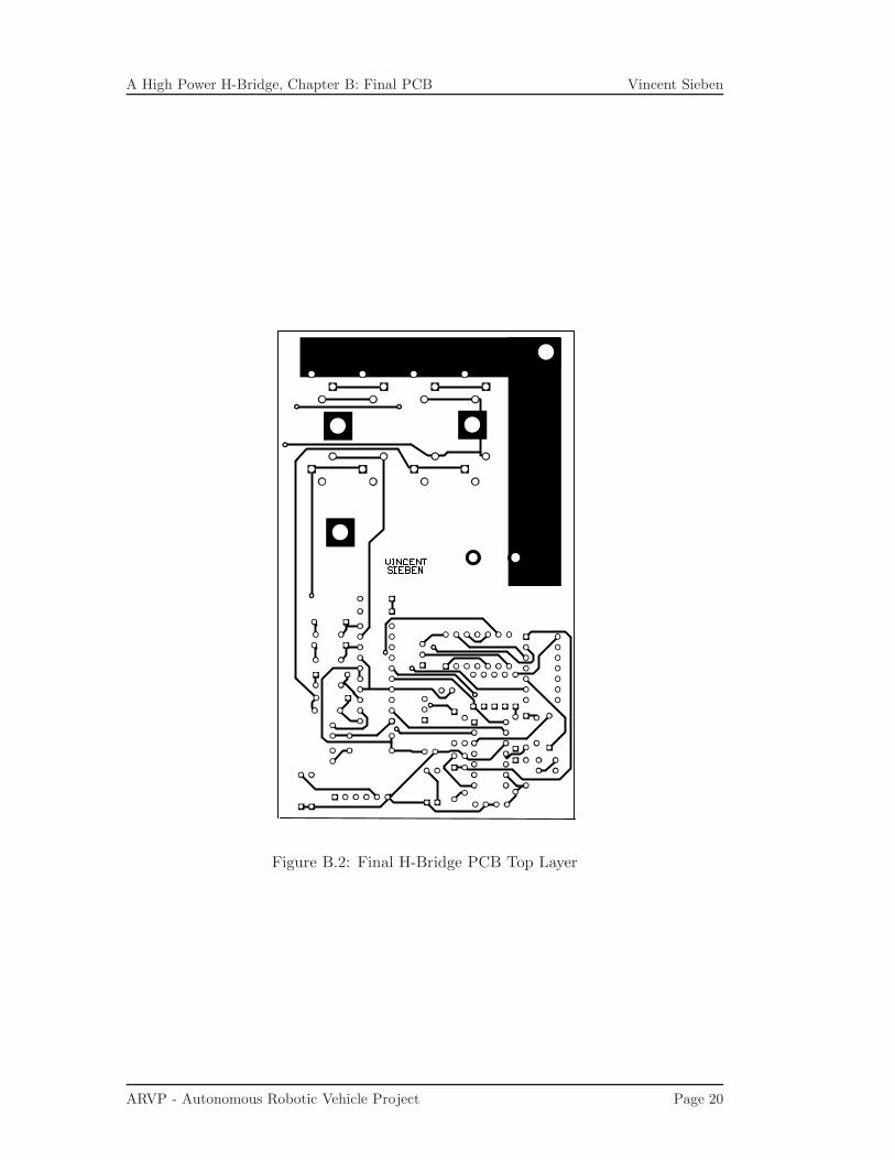
Figure B.2: Final H-Bridge PCB Top Layer
ARVP - Autonomous Robotic Vehicle Project Page 20
A High Power H-Bridge, Chapter B: Final PCB Vincent Sieben
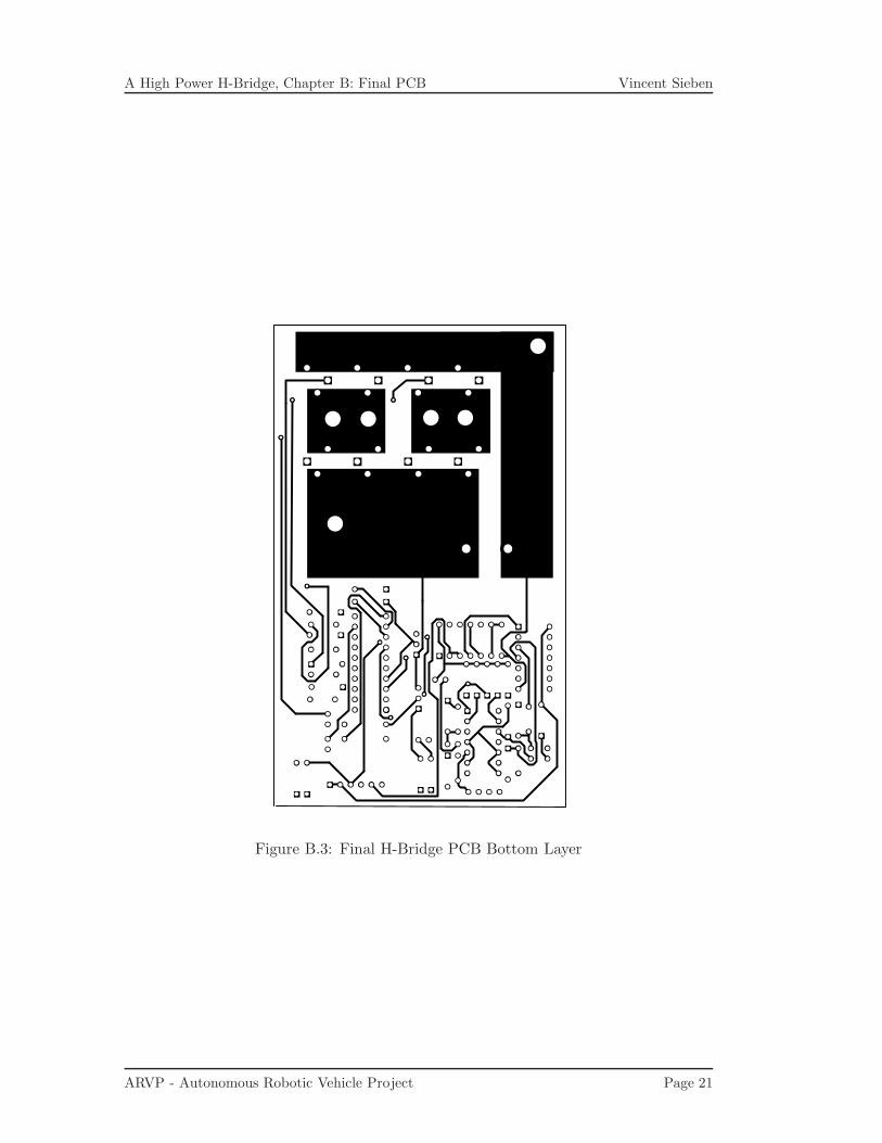
Figure B.3: Final H-Bridge PCB Bottom Layer
ARVP - Autonomous Robotic Vehicle Project Page 21
Appendix C
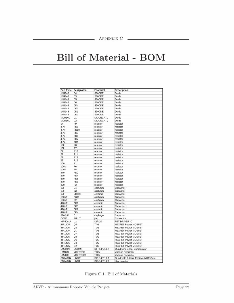
Bill of Material - BOM
Part Type Designator Footprint Description1N4148 D4 SDIODE Diode1N4148 D3 SDIODE Diode1N4148 D5 SDIODE Diode1N4148 D6 SDIODE Diode1N4148 DD4 SDIODE Diode1N4148 DD3 SDIODE Diode1N4148 DD1 SDIODE Diode1N4148 DD2 SDIODE DiodeMUR160 D1 DIODE0.4_V DiodeMUR160 D2 DIODE0.4_V Diode1k R9 resistor resistor4.7k RD5 resistor resistor4.7k RD10 resistor resistor4.7k RD3 resistor resistor4.7k RD9 resistor resistor4.7k RD7 resistor resistor4.7k RD1 resistor resistor10k R8 resistor resistor10k R7 resistor resistor22 R10 resistor resistor22 R11 resistor resistor22 R13 resistor resistor22 R12 resistor resistor100 R1 resistor resistor100k R6 resistor resistor100k R5 resistor resistor470 RD2 resistor resistor470 RD4 resistor resistor470 RD6 resistor resistor470 RD8 resistor resistor820 R2 resistor resistor1uF C4 cap5mm Capacitor1uF C3 cap5mm Capacitor1uF CDelay ceramic Capacitor100uF C300 cap5mm Capacitor100uF C2 cap5mm Capacitor470pF CD1 ceramic Capacitor470pF CD3 ceramic Capacitor470pF CD2 ceramic Capacitor470pF CD4 ceramic Capacitor2200uF C1 caplarge CapacitorCON6 INPUT jtag ConnectorHIP4081A U2 DIP-20 FET DRIVER ICIRF1405 Q5 TO1 HEXFET Power MOSFETIRF1405 Q3 TO1 HEXFET Power MOSFETIRF1405 Q1 TO1 HEXFET Power MOSFETIRF1405 Q7 TO1 HEXFET Power MOSFETIRF1405 Q8 TO2 HEXFET Power MOSFETIRF1405 Q6 TO2 HEXFET Power MOSFETIRF1405 Q4 TO2 HEXFET Power MOSFETIRF1405 Q2 TO2 HEXFET Power MOSFETLM339N UCOMP DIP-14/D19.7 Quad Differential ComparatorLM1084 VOLTREG TOG Voltage RegulatorLM7805 VOLTREG3 TOG Voltage RegulatorSN7402N UNOR DIP-14/D19.7 Quadruple 2-Input Positive-NOR GateSN7404N UNOT DIP-14/D19.7 Hex Inverter
Figure C.1: Bill of Materials
ARVP - Autonomous Robotic Vehicle Project Page 22
Related Documents