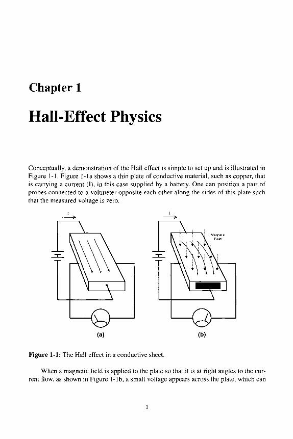
Chapter 1 Hall-Effect Physics Conceptually, a demonstration of the Hall effect is simple to set up and is illustrated in Figure 1-1. Figure 1-la shows a thin plate of conductive material, such as copper, that is carrying a current (I), in this case supplied by a battery. One can position a pair of probes connected to a voltmeter opposite each other along the sides of this plate such that the measured voltage is zero. I / \ -!- \ I f Q (a) (b) Figure 1-1: The Hall effect in a conductive sheet. When a magnetic field is applied to the plate so that it is at right angles to the cur- rent flow, as shown in Figure 1-lb, a small voltage appears across the plate, which can

Welcome message from author
This document is posted to help you gain knowledge. Please leave a comment to let me know what you think about it! Share it to your friends and learn new things together.
Transcript
Chapter 1
Hall-Effect Physics
Conceptually, a demonstration of the Hall effect is simple to set up and is illustrated in Figure 1-1. Figure 1-la shows a thin plate of conductive material, such as copper, that is carrying a current (I), in this case supplied by a battery. One can position a pair of probes connected to a voltmeter opposite each other along the sides of this plate such that the measured voltage is zero.
I /
\
- ! -
\
I f
Q (a) (b)
Figure 1-1: The Hall effect in a conductive sheet.
When a magnetic field is applied to the plate so that it is at right angles to the cur- rent flow, as shown in Figure 1-lb, a small voltage appears across the plate, which can
CHAPTER I. HALL-EFFECT PHYSICS
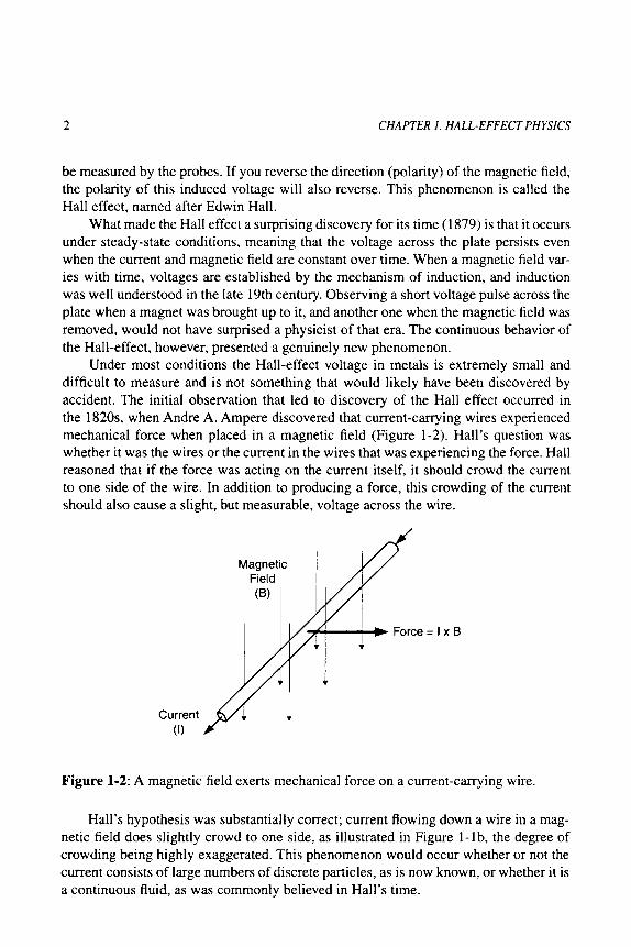
be measured by the probes. If you reverse the direction (polarity) of the magnetic field, the polarity of this induced voltage will also reverse. This phenomenon is called the Hall effect, named after Edwin Hall.
What made the Hall effect a surprising discovery for its time (1879) is that it occurs under steady-state conditions, meaning that the voltage across the plate persists even when the current and magnetic field are constant over time. When a magnetic field var- ies with time, voltages are established by the mechanism of induction, and induction was well understood in the late 19th century. Observing a short voltage pulse across the plate when a magnet was brought up to it, and another one when the magnetic field was removed, would not have surprised a physicist of that era. The continuous behavior of the Hall-effect, however, presented a genuinely new phenomenon.
Under most conditions the Hall-effect voltage in metals is extremely small and difficult to measure and is not something that would likely have been discovered by accident. The initial observation that led to discovery of the Hall effect occurred in the 1820s, when Andre A. Ampere discovered that current-carrying wires experienced mechanical force when placed in a magnetic field (Figure 1-2). Hall's question was whether it was the wires or the current in the wires that was experiencing the force. Hall reasoned that if the force was acting on the current itself, it should crowd the current to one side of the wire. In addition to producing a force, this crowding of the current should also cause a slight, but measurable, voltage across the wire.
Current (I)
e = l x B
Magnetic Field (B)
Figure 1-2: A magnetic field exerts mechanical force on a current-carrying wire.
Hall's hypothesis was substantially correct; current flowing down a wire in a mag- netic field does slightly crowd to one side, as illustrated in Figure 1-1 b, the degree of crowding being highly exaggerated. This phenomenon would occur whether or not the current consists of large numbers of discrete particles, as is now known, or whether it is a continuous fluid, as was commonly believed in Hall's time.
I.I. A QUANTITATIVE EXAMINATION
1.1 A Quantitative Examination Enough is presently known about both electromagnetics and the properties of various materials to enable one to analyze and design practical magnetic transducers based on the Hall effect. Where the previous section described the Hall effect qualitatively, this section will attempt to provide a more quantitative description of the effect and to relate it to fundamental electromagnetic theory.
In order to understand the Hall effect, one must understand how charged particles, such as electrons, move in response to electric and magnetic fields. The force exerted on a charged particle by an electromagnetic field is described by:
F = qo E + qo ~ • B (Equation I- I)
where P is the resultant force, E is the electric field, ~ is the velocity of the charge,
/3 is the magnetic field, and q0 is the magnitude of the charge. This relationship is com- monly referred to as the Lorentz force equation. Note that, except for q0, all of these variables are vector quantities, meaning that they contain independent x, y, and z com- ponents. This equation represents two separate effects: the response of a charge to an electric field, and the response of a moving charge to a magnetic field.
In the case of the electric field, a charge will experience a force in the direction of the field, proportional both to the magnitude of the charge and the strength of the field. This effect is what causes an electric current to flow. Electrons in a conductor are pulled along by the electric field developed by differences in potential (voltage) at different points.
In the case of the magnetic field, a charged particle doesn't experience any force unless it is moving. When it is moving, the force experienced by a charged particle is a function of its charge, the direction in which it is moving, and the orientation of the magnetic field it is moving through. Note that particles with opposite charges will experience force in opposite directions; the signs of all variables are significant. In the simple case where the velocity is at fight angles to the magnetic field, the force exerted is at right angles to both the velocity and the magnetic field. The cross-product operator ( x ) describes this relationship exactly. Expanded out, the force in each axis (x,y,z) is related to the velocity and magnetic field components in the various axes by"
F -qo(vyBz-vzBy )
F = q o ( v z B - v z B x )
F =qo(vxBy-VyBx) (Equation 1-2)

CHAPTER 1. HALL-EFFECT PHYSICS
The forces a moving charge experiences in a magnetic field cause it to move in curved paths, as depicted in Figure 1-3. Depending on the relationship of the velocity to the magnetic field, the motion can be in circular or helical patterns.
f /
/
/ X X/ f - - - ~ X
\
t / X X \
X X
Sx x / X ~ X
X
~ X -1 l i l i I
(a) (b)
Figure 1-3" Magnetic fields cause charged particles to move in circular (a) or helical (b) paths.
In the case of charge carriers moving through a Hall transducer, the charge carrier velocity is substantially in one direction along the length of the device, as shown in Figure 1-4, and the sense electrodes are connected along a perpendicular axis across the width. By constraining the carrier velocity to the x axis (vy = O, vz = 0) and the sensing of charge imbalance to the z axis, we can simplify the above three sets of equations to one:
F = qovxB, (Equation 1-3)
which implies that the Hall-effect transducer will be sensitive only to the y component of the magnetic field. This would lead one to expect that a Hall-effect transducer would be orientation sensitive, and this is indeed the case. Practical devices are sensitive to magnetic field components along a single axis and are substantially insensitive to those components on the two remaining axes. (See Figure 1-4.)
Although the magnetic field forces the charge carriers to one side of the Hall trans- ducer, this process is self-limiting, because the excess concentration of charges to one side and consequent depletion on the other gives rise to an electric field across the transducer. This field causes the carriers to try to redistribute themselves more evenly. It also gives rise to a voltage that can be measured across the plate. An equilibrium develops where the magnetic force pushing the charge carriers aside is balanced out by the electric force trying to push them back toward the middle

1.2. HALL EFFECT IN METALS
/•-/M Applied agnetic Field.
Length / / i i 'L' U / / C a r r i e r / , ~ ~ ( / / / / / Drift Ve,ocity/ / /
Th'c ?essI [ I// I_.. ~1 I~" Width 'W' Vl
Sense ~ r /jTerminals f~ T~176
Y
Figure 1-4: Hall-effect transducer showing critical dimensions and reference axis.
qo E n + qo v • B = 0 (Equat ion 1-4)
where En is the Hall electric field across the transducer. Solving for En yields
E H - - v x B (Equat ion 1-5)
which means that the Hall field is solely a function of the velocity of the charge carriers and the strength of the magnetic field. For a transducer with a given width w between sense electrodes, the Hall electric field can be integrated over w, assuming it is uniform, giving us the Hall voltage.
V H = - w v B (Equation 1-6)
The Hall voltage is therefore a linear function of: a) the charge carrier velocity in the body of the transducer, b) the applied magnetic field in the "sensitive" axis, c) the spatial separation of the sense contacts, at right angles to carrier motion.
1.2 Hall Effect in Metals
To estimate the sensitivity of a given Hall transducer, it is necessary to know the aver- age charge carrier velocity. In a metal, conduction electrons are free to move about and do so at random because of their thermal energy. These random "thermal velocities" can be quite high for any given electron, but because the motion is random, the motions
CHAPTER 1. HALL-EFFECT PHYSICS
of individual electrons average out to a zero net motion, resulting in no current. When an electric field is applied to a conductor, the electrons "drift" in the direction of the applied field, while still performing a fast random walk from their thermal energy. This average rate of motion from an electric field is known as drift velocity.
In the case of highly conductive metals, drift velocity can be estimated. The first step is to calculate the density of carriers per unit volume. In the case of a metal such as copper, it can be assumed that every copper atom has one electron in its outer shell that is available for conducting electric current. The volumetric carrier density is therefore the product of the number of atoms per unit of weight and the specific gravity. For the case of copper this can be calculated:
N = N A D = 6.02 x 10²³ mol -~
M m 63.55g. mol -~ • 8.89g. cm -3 = 8.42 x 1022 cm -3 (Equat ion 1-7)
where: N is the number of carriers per cubic centimeter NA is the Avogadro constant (6.02 • 23 mol -~) Mm is the molar mass of copper (63.55 g . mol -~) D is specific gravity of copper (grams/cm3)
Once one has the carrier density, one can estimate the carrier drift velocity based on current. The unit of current, the ampere (A), is defined as the passage of =6.2 x 10¹⁸ charge carriers per second and is equal to 1/qO. Consider the case of a piece of conductive material with a given cross-sectional area of A. The carrier velocity will be proportional to the current, as twice as much current will push twice as many carriers through per unit time. Assuming that the carrier density is constant and the carriers behave like an incompressible fluid, the velocity will also be inversely proportional to the cross section, a larger cross section meaning lower carrier velocity. The carrier drift velocity can be determined by:
I v = ~ ( E q u a t i o n 1 - 8 )
qoNA
where v is carrier velocity, cm/sec I is current in amperes Q0 is the charge on an electron (1.60 x 10 -19 C) N is the carrier density, carriers/cm 3 A is the cross section in cm 2 One surprising result is the drift velocity of carriers in metals. While the electric
field that causes the charge carriers to move propagates through a conductor at ap- proximately half the speed of light (300 x 10 6 m]s) , the actual carriers move along at a much more leisurely average pace. To get an idea of the disparity, consider a piece of

1.3. THE HALL EFFECT IN SEMICONDUCTORS
#18 gauge copper wire carrying one ampere. This gauge of wire is commonly used for wiring lamps and other household appliances and has a cross section of about 0.0078 cm 2. One ampere is about the amount of current required to light a 100-watt light bulb. Using the previously derived carrier density for copper and substituting into the previ- ous equation gives:
IA v = = 0.009 cm. s -~ (Equation 1-9)
1.6 • 10 -19C. 8.42 • 10 22cm -3- 0.0078 cm2
The carrier drift velocity in the above example is considerably slower than the speed of light; in fact, it is considerably slower than the speed of your average garden snail.
By combining Equations (1-6) and (1-8), we can derive an expression that de- scribes the sensitivity of a Hall transducer as a function of cross-sectional dimensions, current, and carrier density:
/B V. = ~ (Equat ion 1-10)
qoNd
where d is the thickness of the conductor. Consider the case of a transducer consisting of a piece of copper foil, similar to
that shown back in Figure 1-1. Assume the current to be 1 ampere and the thickness to be 25 ~m (0.001 "). For a magnetic field of 1 tesla (10,000 gauss) the resulting Hall voltage will be:
_ 1A. 1T = 3 . 0 • 1 0 - r v (Equat ion 1-11) Vn - 1.6 • 10 -19 C. 8.42 x 1028 m -3. 25 x 10 -6 m
Note the conversion of all quantities to SI (meter-kilogram-second) units for con- sistency in the calculation.
Even for the case of a magnetic field as strong as 10,000 gauss, the voltage result- ing from the Hall effect is extremely small. For this reason, it is not usually practical to make Hall-effect transducers with most metals.
1.3 The Hall Effect in Semiconductors
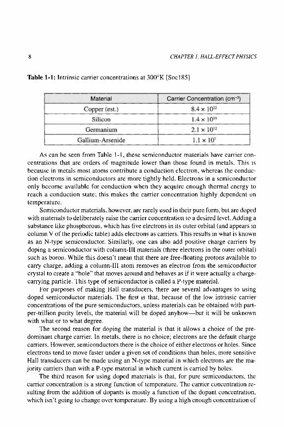
From the previous description of the Hall effect in metals, it can be seen that one means of improvement might be to find materials that do not have as many carriers per unit volume as metals do. A material with a lower carrier density will exhibit the Hall effect more strongly for a given current and depth. Fortunately, semiconductor materials such as silicon, germanium, and gallium-arsenide provide the low carrier densities needed to realize practical transducer elements. In the case of semiconductors, cartier density is usually referred to as carrier concentration.
CHAPTER I. HALL-EFFECT PHYSICS
Table 1-1: Intrinsic carrier concentrations at 300~ [Soc185]
Material Carrier Concentration (cm -3)
Copper (est.) 8.4 x 1 0 22
Silicon 1.4 x 10 ~~
Germanium 2.1 • 1012
Gallium-Arsenide 1.1 x 10⁷
As can be seen from Table 1-1, these semiconductor materials have carrier con- centrations that are orders of magnitude lower than those found in metals. This is because in metals most atoms contribute a conduction electron, whereas the conduc- tion electrons in semiconductors are more tightly held. Electrons in a semiconductor only become available for conduction when they acquire enough thermal energy to reach a conduction state; this makes the carrier concentration highly dependent on temperature.
Semiconductor materials, however, are rarely used in their pure form, but are doped with materials to deliberately raise the carrier concentration to a desired level. Adding a substance like phosphorous, which has five electrons in its outer orbital (and appears in column V of the periodic table) adds electrons as carriers. This results in what is known as an N-type semiconductor. Similarly, one can also add positive charge carriers by doping a semiconductor with column-III materials (three electrons in the outer orbital) such as boron. While this doesn't mean that there are flee-floating protons available to carry charge, adding a column-III atom removes an electron from the semiconductor crystal to create a "hole" that moves around and behaves as if it were actually a charge- carrying particle. This type of semiconductor is called a P-type material.
For purposes of making Hall transducers, there are several advantages to using doped semiconductor materials. The first is that, because of the low intrinsic carrier concentrations of the pure semiconductors, unless materials can be obtained with part- per-trillion purity levels, the material will be doped anyhow--but it will be unknown with what or to what degree.
The second reason for doping the material is that it allows a choice of the pre- dominant charge carrier. In metals, there is no choice; electrons are the default charge carriers. However, semiconductors there is the choice of either electrons or holes. Since electrons tend to move faster under a given set of conditions than holes, more sensitive Hall transducers can be made using an N-type material in which electrons are the ma- jority carriers than with a P-type material in which current is carried by holes.
The third reason for using doped materials is that, for pure semiconductors, the carrier concentration is a strong function of temperature. The carrier concentration re- sulting from the addition of dopants is mostly a function of the dopant concentration, which isn't going to change over temperature. By using a high enough concentration of
1.4 A SILICON HALL-EFFECT TRANSDUCER
dopant, one can obtain relatively stable carrier concentrations over temperature. Since the Hall voltage is a function of carrier concentration, using highly doped materials results in a more temperature-stable transducer.
In the case of Hall transducers on integrated circuits, there is one more reason for using doped silicon--mainly because that's all that is available. The various silicon lay- ers used in common IC processes are doped with varying levels of N and P materials, depending on their intended function. Layers of pure silicon are not usually available as part of standard IC fabrication processes.
1.4 A Silicon Hall-Effect Transducer
Consider a Hall transducer constructed from N-type silicon that has been doped to a level of 3 • 10 ~5 cm -3. The thickness is 251am and the current is 1 mA. By substituting the relevant numbers into Equation 1-10, we can calculate the voltage output for a l- tesla field:
0.001A. 1T = = 0.083V (Equat ion 1-12)
Vn 1.6x 10⁻¹⁹C.3x 1021 m-3.25 x 10⁻⁶m
The resultant voltage in this case is 83 mV, which is more than 20,000 times the signal of the copper transducer described previously. Equally significant is that the necessary bias current is 1/1000 that used to bias the copper transducer. Millivolt-level output signals and milliamp-level bias currents make for practical sensors.
While one can calculate transducer sensitivity as a function of geometry, doping levels, and bias current, there is one detail we have ignored to this point: the resistance of the transducer. While it is possible to get tremendous sensitivities from thinly doped semiconductor transducers for milliamps of bias current, it may also require hundreds of volts to force that current through the transducer. The resistance of the Hall trans- ducer is a function of the conductivity and the geometry; for a rectangular slab, the resistance can be calculated by:
R = ~ (Equat ion 1-13) w . d
where R is resistance in ohms
is the resistivity in ohm-cm I is the length in cm w is the width in cm d is the thickness in cm
10 CHAPTER 1. HALL-EFFECT PHYSICS
In the case of metals, ~ is a characteristic of the material. In the case of a semi- conductor, however, ~ is a function of both the doping and a property called cartier mobility. Carrier mobility is a measure of how fast the charge carriers move in response to an electric field, and varies with respect to the type of semiconductor, the dopant concentration level, the carrier type (N or P type), and temperature.
In the case of the silicon Hall-effect transducer described above (d = 25 lam = 0.0025 cm), made from N-type silicon doped to a level of 3 x 1015cm -3, r = 1.7 ~2-cm at room temperature. Let us also assume that the transducer is 0.1 cm long and 0.05 cm wide. The resistance of this transducer is given by:
~ . I 1.7f~. cm • 0.1 cm R . . . . 1360f~ (Equat ion 1-14)
w-d 0.05 c m x 0.0025 cm
With a resistance of 1360fL it will take 1.36V to force 1 mA of current through the device. This results in a power dissipation of 1.36 mW, a modest amount of power that can be easily obtained in many electronic systems. The sensitivity and power con- sumption offered by Hall-effect transducers made from silicon or other semiconductors makes them practical sensing devices.

Chapter 2
Practical Transducers
In the last chapter we examined the physics of a Hall-effect transducer and related its performance to physical characteristics and materials properties. While this level of detail is essential for someone designing a Hall-effect transducer, it is not necessary for someone attempting to design with an already existing and adequately characterized device.
2.1 Key Transducer Characteristics
What are the key characteristics of a Hall-effect transducer that should be considered by a sensor designer? For the vast majority of applications, the following characteristics describe a Hall-effect transducer's behavior to a degree that will allow one to design it into a larger system.
�9 Sensitivity �9 Temperature coefficient (tempco) of sensitivity �9 Ohmic offset �9 Temperature coefficient of ohmic offset �9 Linearity �9 Input and output resistance �9 Temperature coefficient of resistance �9 Electrical output noise
Sensitivity Transducer sensitivity, or gain, was the major focus of much of the last chapter, in which we analyzed the device physics. From a designer's standpoint, more sensitivity is usually a good thing, as it increases the amount of signal available to work with. A
12 CHAPTER 2. PRACTICAL TRANSDUCERS
sensor that provides more output signal often require simplers and less expensive sup- port electronics than one with a smaller output signal.
Because the sensitivity of a Hall-effect transducer is dependent on the amount of current used to bias it, the sensitivity of a device needs to be described in a way that takes this into account. Sensitivity can be characterized in two ways:
1. Volts per unit field, per unit of bias current (V/B x I) 2. Volts per unit field, per unit of bias voltage (l/B)
Since a Hall-effect transducer is almost always biased with a constant current, the first characterization method provides the most detailed information. Characterizing by bias voltage, however, is also useful in that it quickly tells you the maximum sensitivity that can be obtained from that transducer when it is used in a bias circuit operating from a given power-supply voltage.
Temperature Coefficient of Sensitivity
Although a Hall-effect transducer has a fairly constant sensitivity when operated from a constant current source, the sensitivity does vary slightly over temperature. While these variations are acceptable for some applications, they must be accounted for and corrected when a high degree of measurement stability is needed. Figure 2-1 shows the variation in sensitivity for an EW. Bell BH-200 instrumentation-quality indium-arse- nide Hall-effect transducer when biased with a constant current. The mean temperature coefficient of sensitivity of this device is about -0.08%/~
+4-'
O~
% C h a n g e in
Sens i t iv i ty
- 4 -
-8 I I I I �9 -40 ~ 0 ~ 40 ~ 80 ~ 120 ~
T e m p e r a t u r e ~
Figure 2-1- Sensitivity vs. temperature for BH-series Hall transducer under constant current bias (after [Bell]).
2.1. KEY TRANSDUCERS CHARACTERISTICS 13
When operating a Hall-effect transducer from a constant-voltage bias source, one will obtain sensitivity variations over temperature considerably greater than those ob- tained when operating the device from a constant-current bias source. For this reason constant-current bias is normally used when one is concerned with the temperature stability of the sensor system. For the BH-200 device described above, constant-volt- age bias would result in a temperature coefficient of sensitivity of approximately -0.2%/~
Ohmic Offset
Because we live in an imperfect world, we can't expect perfection in our transducers. When a Hall-effect transducer is biased, a small voltage will appear on the output even in the absence of a magnetic field. This offset voltage is undesirable, because it limits the ability of the transducer to discriminate small steady-state magnetic fields. A num- ber of effects conspire to create this offset voltage. The first is alignment error of the sense contacts, where one is further "upstream" or "downstream" in the bias current than the other, lnhomogeneities in the material of the transducer can be another source. These effects are illustrated in Figure 2-2. Finally, the semiconductor materials used to make Hall-effect transducers are highly piezoresistive, meaning that the electrical re- sistance of the material changes in response to mechanical distortion. This causes most Hall-effect transducers to behave like strain gauges in response to mechanical stresses imposed on them by the packaging and mounting.
Contact Mis-alignment " ~
L Inhomogeneity
Figure 2-2: Ohmic offsets result from misalignment of the sense contacts and inhomo- geneities in the material.
14 CHAPTER 2. PRACTICAL TRANSDUCERS
Although offset is usually expressed in terms of output voltage for a given set of bias conditions, it also needs to be considered in terms of magnetic field units. For ex- ample, compare a transducer with 500 l.tV of offset and a sensitivity of 100 ~V/gauss, to a second transducer with 200 I.tV of offset but only 10 l.tV/gauss of sensitivity. The first transducer has a 5-gauss offset while the latter has an offset of 20 gauss, in addition to having a much lower sensitivity. For applications where low magnetic field levels are to be measured, the first sensor would tend to be easier to use, both because it provides a higher sensitivity and also because it provides a lower offset error when considered in terms of the quantity being measured, namely magnetic field.
Temperature Coefficient of Ohmic Offset
Like sensitivity, the offset of a transducer will drift over temperature. Unlike sensitiv- ity, however, the offset drift will tend to be random, varying from device to device, and is not generally predictable. Some offset drift results from piezoresistive effects in the transducer. As temperature varies, uneven expansion of the materials used to fabricate a transducer will induce mechanical stresses in the device. These stresses are then sensed by the Hall-effect transducer. In general, devices with larger initial offsets also tend to have higher levels of offset drifts. While there are techniques for minimizing offset and its drift, precision applications often require that each transducer be individually characterized over a set of environmental conditions and a compensation scheme be set for that particular transducer.
Linearity
Because Hall-effect transducers are fundamentally passive devices, much like strain gauges, the output voltage cannot exceed the input voltage. This results in a roll-off of sensitivity as the output voltage approaches even a small fraction of the bias voltage. In cases where the Hall voltage is small in comparison to the transducer bias voltage, Hall sensors tend to be very linear, with linearity errors of less than 1% over significant op- erating ranges. When constructing instrumentation-grade sensors, which are expected to measure very large fields such as 10,000 or even 100,000 gauss, it is often desirable to use low sensitivity devices that do not easily saturate.
Input and Output Resistances
These parameters are of special interest to the circuit designer, as they influence the design of the bias circuitry and the front-end amplifier used to recover the transducer signal. The input resistance affects the design of the bias circuitry, while the output re- sistance affects the design of the amplifier used to detect the Hall voltage. Although it is possible to design a front-end amplifier with limited knowledge of the resistance of the signal source that will be feeding it, it may be far from optimal from either performance
2.1. KEY TRANSDUCERS CHARACTERISTICS 15
or cost standpoints, compared to an amplifier designed in light of this information. For low-noise applications, the output resistance is of special interest, since one
source of noise, to be discussed later, is dependent on the output resistance of the de- vice. A simple electrical model describing a Hall-effect transducer from a circuit-inter- face standpoint is presented later on in Chapter 3.
Temperature Coefficient of Resistance
The temperature coefficient of the input and output resistances will either be identi- cal, or match ver3' closely. Knowing thc tcmpcrature variation of the input resistance is useful when designing the current source used to bias the transducer. For transduc- ers biased with a constant current source, the bias voltage will be proportional to the transducer's resistance. A bias circuit designed to drive a transducer with a particular resistance at room temperature may fail to do so at hot or cold extremes if variations in transducer resistance are not anticipated. For practical transducers the temperature co- efficient of resistance can be quite high, often as much as 0.3 %/~ Over an automotive temperature range (-50 ~ to +125~ this means that the input and output resistances can vary by as much as 30% from their room temperature values.
Noise
In addition to providing a signal voltage, Hall-effect transducers also present electrical noise at their outputs. For now we will limit our discussion to sources of noise actually generated by the transducer itself, and not those picked up from the outside world or developed in the amplifier electronics.
The most fundamental and unavoidable of electrical noise sources is called John- son noise, and it is the result of the thermally induced motion of electrons (or other charge carriers) in a conductive material. It is solely a function of the resistance of the device and the operating temperature. Johnson noise is generated by any resistance (including that found in a Hall transducer), and is described by:
V = 44kTRB (Equation 2-1)
where k is Boltzmann's constant (1.38 x 10 -23 K -t) T is absolute temperature in ~ R is resistance in ohms B is bandwidth in hertz
The bandwidth over which the signal is examined is an important factor in how much noise is seen. The wider the frequency range over which the signal is examined, the more noise will be seen.

16 CHAPTER 2. PRACTICAL TRANSDUCERS
The down side of Johnson noise is that it defines the rock-bottom limit of how small a signal can be recovered from the transducer. The two positive aspects are that it can be minimized by choice of transducer impedance, and that it is not usually of tremendous magnitude. A 1-kf~ resistor, for example, at room temperature (300~ will only generate about 400 nanovolts RMS (root-mean-squared) of Johnson noise measured across a 10-kilohertz bandwidth.
Flicker noise, also known as 1/f noise, is often a more significant problem than Johnson noise. This type of noise is found in many physical systems, and can be gener- ated by many different and unrelated types of mechanisms. The common factor, how- ever, is the resultant spectrum. The amount of noise per unit of bandwidth is, to a first approximation, inversely proportional to the frequency; this is why it's also referred to as 1/f noise. Because many sensor applications detect DC or near-DC low-frequency signals, this type of noise can be especially troublesome. Unlike Johnson noise, which is intrinsic to any resistance regardless of how it was constructed, the flicker noise de- veloped by a transducer is related to the specific materials and fabrication techniques used. It is therefore possible to minimize it by improved materials and processes.
The following sections describe the construction and characteristics of several types of Hall-effect transducers that are presently in common use.
2.2 Bulk Transducers
A bulk-type transducer is essentially a slab of semiconductor material with connections to provide bias and sense leads to the device. The transducer is cut and ground to the desired size and shape and the wires are attached by soldering or welding. One advan- tage of bulk-type devices is that one has a great deal of choice in selecting materials. Another advantage is that the large sizes of bulk transducers result in lower impedance levels and consequently lower noise levels than those offered by many other processes. Some key characteristics of an instrument-grade bulk indium-arsenide transducer (the EW. Bell BH-200) are shown in Table 2-1.
Table 2-1" Key characteristics of B H-200 Hall Transducer
Characteristic Value Units
Nominal bias current 150 mA
Sensitivity at recommended bias current (Ibias = 150 mA) ~ 15 IuV/G
Sensitivity (current referenced) ~ 100 laV/G.A
Temperature coefficient of sensitivity 0.08 %/~
Ohmic offset, electrical (maximum) (Ibias = 150 mA) _100 ~V
Ohmic offset, magnetic (maximum) ~ ___7 gauss
Tempco of ohmic offset, electrical (Ibias = 150 mA) +_ 1 IaV/~ (Continued)

2.2. BULK TRANSDUCERS 17
Characteristic Value Units Tempco of ohmic offset, magnetic I +0.07 ___gauss/~
Max linearity error (over __+ 10 kilogauss) __+ 1 %
Input resistance (max) 2.5 f2
Output resistance (max) 2 f2
Temperature coefficient of resistance 0.15 %/~
Note 1" These parameters estimated from manufacturer's data
2.3 Thin-Film Transducers
A thin-film transducer is constructed by depositing thin layers of metal and semicon- ductor materials on an insulating support structure, typically alumina (A1203) or some other ceramic material. Figure 2-3 provides an idealized structural view of a "typical" thin-film Hall-effect transducer. The thickness of the films used to fabricate these de- vices can be on the order of 1 ~tm or smaller.
I I | I
I I
I !
Copper contact Semiconductor
Ceramic Substrate
(a) (b)
Figure 2-3: Schematic top (a) and cross-section (b) views of thin-film Hall-effect transducer.
The primary advantages of thin-film construction are: �9 Flexibility in material selection �9 Small transducer sizes achievable �9 Thin Hall-effect transducers provide more signal for less bias current �9 Photolithographic processing allows for mass production

18 CHAPTER 2. PRACTICAL TRANSDUCERS
Each layer is added to the thin-film device by a process that consists of covering the device with the film and selectively removing the sections that are not wanted, leav- ing the desired patterns. The details of the processing operations for each layer vary depending on the characteristics of the materials being used.
Film deposition is commonly accomplished through a number of means, the two most common being evaporation and sputtering. In evaporation, the substrate to be coated and a sample of the coating material are both placed in a vacuum chamber, as shown in Figure 2-4. The sample is then heated to the point where it begins to vaporize into the vacuum. The vapor then condenses on any cooler objects in the chamber, such as the substrate to be coated. Because the hot vapor in many cases will chemically react with any stray gas molecules, a substantially good vacuum is required to implement this technique. Vacuums of 10 -6 to 10 -7 torr (760 torr = 1 atmosphere) are commonly required for this type of process. The thickness of the deposited film is controlled by the exposure time.
Vacuum Jar
,__ Target
Sample
x" A .,
,. ! .. .,/'
., ./
/
4
?
.! .!
/ /
, .,..
Figure 2-4: Schematic drawing of evaporative thin-film process.
Sputtering is another method for coating substrates with thin films. In sputtering, the sample coating material is not directly heated. Instead, an inert gas, such as argon, is ionized into a plasma by an electrical source. The velocity of the ions of the plasma is sufficient to knock atoms out of the coating sample (the target), at which point they can deposit themselves on the substrate to be coated. As in the case of an evaporative coat- ing system, film thickness is controlled by exposure time. Figure 2-5 shows a schematic view of a sputtering system.

2.3. THIN-FILM TRANSDUCERS 19
Process Gas Inlet
Vacuum Pump
Vacuum Housing
Target~k'~ /
I I o
t
o o
�9 P l a s m a . t .
i i
Substrate~, ' , , , , , j ; . . . . . . . . . . . . . . ; . .
Work Holder J
R F
urce
Figure 2-5: Sputtering method of thin-film deposition.
The principal advantage offered by sputtering over evaporation is that, because the coating material doesn't need to be heated to near its evaporation point, it is possible to make thin films with a much wider variety of materials than is possible by evaporation.
Once a material has been laid down in a thin film, it is then pattemed with a photore- sist material, exposed to a photographic plate carrying the desired pattem, and the photo- resist is then developed, leaving areas of the substrate selectively exposed. The substrate is then etched, often by immersion in a suitable liquid solvent or acid. Alternatively, the substrate can be plasma-etched by a process related to sputtering. In either case, after the etching step is finished, the remaining photoresist is stripped and the substrate is prepared to receive the next layer of film or readied for final processing. The sequence of opera- tions needed to process a layer of a thin film is summarized in Figure 2-6.
S T A R T )
Develop Photoresist
Deposit Film Coat with Photoresist
Exposure (Patterning)
Etch pattern Strip
remaining Photoresis
( oo.E
Figure 2-6: Thin-film processing sequence.

20 CHAPTER 2. PRACTICAL TRANSDUCERS
The HS- 100 is an example of a commercial thin-film Hall transducer manufactured by EW.BeI1. This device is made with two thin-film layers, a metal layer to provide contacts to the Hall-effect element, and an indium-arsenide thin film that forms the Hall-effect transducer itself. In addition, solder bumps are deposited on the copper to provide connection points to the outside world. Wires may be soldered to these fea- tures, or the device may be placed face down on a printed circuit board or ceramic hybrid circuit, and reflow soldered into place.
Key specifications for the HS- 100 transducer are listed in Table 2-2. The major im- provements over bulk devices are in the area of sensitivity and supply current; the thin- film device is nearly as sensitive as the previously described bulk device (BH-200), and obtains this level of sensitivity with an order of magnitude less supply current needed. The BH-200 bulk device, however, is superior in the areas of offset error and drift over temperature. The principal advantage of the thin-film device is potentially lower cost. Thin-film processing techniques allow a great number of devices to be fabricated simul- taneously and separated into individual units at the end of processing.
Table 2-2: Key characteristics of HS-100 Hall transducer
Characteristic Value Units Nominal bias current 150 mA
Sensitivity at recommended bias current (Ibias = 10 mA) ~ 8 laV/gauss
Sensitivity (current referenced) ~ 800 laV/gaussoA
Temperature coefficient of sensitivity -0.1 %/~
Ohmic offset, electrical (maximum) ___6 mV (Ibias = 10 mA)
Ohmic offset, magnetic (maximum) ~ ___750 Gauss
Tempco of ohmic offset, electrical +10 laV/~
(Ibias = 10 mA)
Tempco of ohmic offset, magnetic ~ _+ 1.25 _gauss/~
Max linearity error (over _+10 kilogauss) %
Input resistance (max) 160 f2
Output resistance (max) 360 f2
Temperature coefficient of resistance 0.1 %/~
Note 1" These parameters estimated from manufacturer's data
2.4 Integrated Hall Transducers
Making a Hall-effect transducer out of silicon, using standard integrated circuit pro- cessing techniques, allows one to build complete sensor systems on a chip. The trans-
2.4. INTEGRATED HALL TRANSDUCERS 21
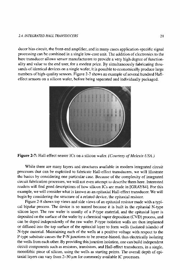
ducer bias circuit, the front-end amplifier, and in many cases application-specific signal processing can be combined in a single low-cost unit. The addition of electronics to the bare transducer allows sensor manufacturers to provide a very high degree of function- ality and value to the end user, for a modest price. By simultaneously fabricating thou- sands of identical devices on a single wafer, it is possible to economically produce large numbers of high-quality sensors. Figure 2-7 shows an example of several hundred Hall- effect sensors on a silicon wafer, before being separated and individually packaged.
Figure 2-7: Hall-effect sensor ICs on a silicon wafer. (Courtesy of Melexis USA.)
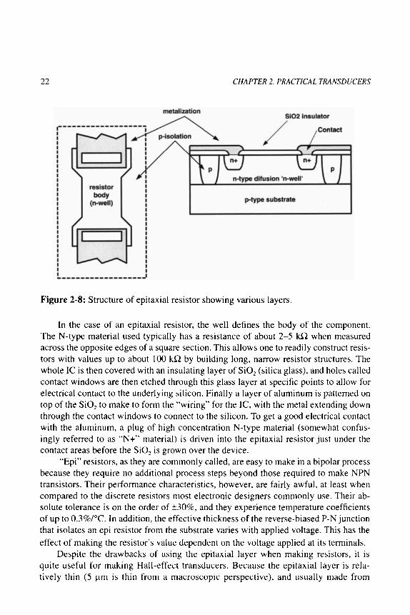
While there are many layers and structures available in modem integrated circuit processes that can be exploited to fabricate Hall-effect transducers, we will illustrate the basics by considering one particular case. Because of the complexity of integrated circuit fabrication processes, we will not even attempt to describe them here. Interested readers will find good descriptions of how silicon ICs are made in [GRAY84]. For this example, we will consider what is known as an epitaxial Hall-effect transducer. We will begin by considering the structure of a related device, the epitaxial resistor.
Figure 2-8 shows top views and side views of an epitaxial resistor made with a typi- cal bipolar process. The device is so named because it is built in the epitaxial N-type silicon layer. The raw wafer is usually of a P-type material, and the epitaxial layer is deposited on the surface of the wafer by a chemical vapor deposition (CVD) process, and can be doped independently of the raw wafer. P-type isolation walls are then implanted or diffused into the top surface of the epitaxial layer to form wells (isolated islands) of N-type material. Maintaining each of the wells at a positive voltage with respect to the P-type substrate causes the P-N junctions to be reverse-biased, thus electrically isolating the wells from each other. By providing this junction isolation, one can build independent circuit components such as resistors, transistors, and Hall-effect transducers, in a single, monolithic piece of silicon, using the wells as starting points. The overall depth of epi- taxial layers can vary from 2-30 ~m for commonly available IC processes.
22 CHAPTER 2. PRACTICAL TRANSDUCERS
metallzation Si02 insulator
: . . . . . . . . . . . . . . . . . . " ; ~ ~ ,Contact
: I resist~ i : : I body I , : | (n-we") I : : j ! i I I I I I I I I I I I I I I I I I I I ! I I
L . . . . . . . . . . . . . . . . . J
p-type substrate
Figure 2-8: Structure of epitaxial resistor showing various layers.
In the case of an epitaxial resistor, the well defines the body of the component. The N-type material used typically has a resistance of about 2-5 kf2 when measured across the opposite edges of a square section. This allows one to readily construct resis- tors with values up to about 100 kf~ by building long, narrow resistor structures. The whole IC is then covered with an insulating layer of SiO2 (silica glass), and holes called contact windows are then etched through this glass layer at specific points to allow for electrical contact to the underlying silicon. Finally a layer of aluminum is patterned on top of the SiO2 to make to form the "wiring" for the IC, with the metal extending down through the contact windows to connect to the silicon. To get a good electrical contact with the aluminum, a plug of high concentration N-type material (somewhat confus- ingly referred to as "N+" material) is driven into the epitaxial resistor just under the contact areas before the SiO2 is grown over the device.
"Epi" resistors, as they are commonly called, are easy to make in a bipolar process because they require no additional process steps beyond those required to make NPN transistors. Their performance characteristics, however, are fairly awful, at least when compared to the discrete resistors most electronic designers commonly use. Their ab- solute tolerance is on the order of +30%, and they experience temperature coefficients of up to 0.3%/~ In addition, the effective thickness of the reverse-biased P-N junction that isolates an epi resistor from the substrate varies with applied voltage. This has the
effect of making the resistor's value dependent on the voltage applied at its terminals. Despite the drawbacks of using the epitaxial layer when making resistors, it is
quite useful for making Hall-effect transducers. Because the epitaxial layer is rela- tively thin (5 ~tm is thin from a macroscopic perspective), and usually made from

2.4. INTEGRATED HALL TRANSDUCERS 23
lightly (N = 10'5/cm 3) doped silicon, it is possible to make reasonably sensitive Hall-ef- fect transducers that have modest power requirements.
Because IC manufacturers view the exact details of their processes as trade secrets and are thus not inclined to broadcast them to the world, we will present an example of a Hall device fabricated with a "generic" bipolar process. This will give a general idea of the performance one can expect from such a device. Figure 2-9 shows the details of this device.
Bias+
VH-
I I
50 um
I I
100um
VH+
Bias-
Figure 2-9: Integrated epitaxial Hall-effect transducer layout.
Note that the connections of the sense terminals are made by bringing out "ears" of epitaxial material from the body of the device and making metal contact at these points, instead of simply placing the sense contacts directly on the transducer. There are two reasons for doing this: the first is to maximize the sensitivity by ensuring that all the bias current flows between the sense terminals, and the second is to minimize ohmic offsets. Because the "ears" are fabricated in the same process step as the rest of the transducer, a high degree of alignment is naturally maintained. Metalization and contact windows, on the other hand, are fabricated in separate manufacturing steps, increasing the opportunities for contact misalignment.
For this transducer, the critical physical parameters are: �9 Length = 200 ~tm �9 Width = 100 ~tm �9 Thickness (of epi layer) = 10 ~tm

24 CHAPTER 2. PRACTICAL TRANSDUCERS
�9 Carder concentration = 3 x 10¹⁵/cm 3 (3 x 10²¹/m 3) �9 Bulk resistivity 0 = 2 f2-cm (0.02 ~ -m)
The sensitivity per unit of current and field can be calculated by using equation 1-10, yielding:
IB 1A.1T . . . . 208 V (Equat ion 2-1)
Vn qoNd 1.6 x 10 -19C" 3 x 10 21m -3" 10 -sm
for 1 tesla at 1 ampere of bias, or 20.8 mV/G-A in cgs units. This is an amazingly high level of sensitivity. This sensor, however, will never operate at one ampere; 1 milliam- pere is a more realistic bias current. Even at 1 milliampere, however, this transducer will still provide 20 l.tV/gauss.
The next major question is that of input and output resistance. Because the bias current flows in a substantially uniform manner between the bias contacts, since the contacts extend across the width of the transducer, we can make a fairly good estimate of the input resistance by:
L 200x lO-6m R~. = o ~ = 0.02f2. m . 0- 5 = 4000f2 (Equat ion 2-2)
W . T 100• 10-6m 1 m
It therefore requires 4V to bias the transducer with 1 mA. Because of geometric factors, the output resistance cannot be as readily calculated
as the input resistance. If one were to apply a voltage between the output terminals, the lines of current flow would not be parallel and uniform (and therefore amenable to back-of-envelope analysis). For purposes of designing a compatible front-end amplifier and noise calculations, one might assume that the resistance of the output is within a factor of two or three of that of the input.
Because the estimation of temperature sensitivities and ohmic offset is very diffi- cult (if not impossible) even when one is working with a fully characterized process, we shall ignore them. Suffice it to say, however, that integrated Hall-effect transducers can be made with substantially good performance in these areas. For sake of comparison with the previous examples, Table 2-3 lists a few of the predicted and "guesstimated" characteristics of our hypothetical integrated transducer.
Table 2-3: Key characteristics of hypothetical silicon integrated Hall-effect transducer
Characteristic Sensitivity at recommended bias current (Ibias = 1 mA)
Value
20
Units
pV/G
Sensitivity (current referenced) 20 mV/GoA
(Continued)

2.4. INTEGRATED HALL TRANSDUCERS 25
Characteristic Value Units Temperature coefficient of sensitivity -0.1 %/~ (for constant-current bias)
Ohmic offset, electrical (maximum) +_ 10 mV (Ibias = 1 mA)
Ohmic offset, magnetic (maximum) _+500 G
Max linearity error (over _+1 kilogauss) 1 %
Input resistance 4000 f~
Output resistance 4000? f~
Temperature coefficient of resistance 0.3 %/~
It is also possible to construct integrated Hall-effect transducers from gallium- arsenide, germanium, and other semiconductor materials for even better performance. Integrated processes based on these other materials, however, do not provide the wealth of electronic device types that can be cofabricated on silicon processes.
Silicon processes have another advantage: availability. High-quality Hall-effect transducers can be fabricated with many standard bipolar and CMOS integrated circuit processes with little or no modification. A number of semiconductor companies pres- ently produce a vast array of Hall-effect integrated circuits.
Figure 2-10 shows an example of a silicon Hall-effect IC, containing a Hall-effect transducer and a number of other components such as transistors and resistors. The Hall-effect transducer is the square-shaped object in the center. The size of this IC is roughly 1.5 mm x 2 mm.
Figure 2-10: Silicon Hall-effect sensor IC with supporting electronics. (Courtesy of Melexis USA.)

26 CHAPTER 2. PRACTICAL TRANSDUCERS
2.5 Transducer Geometry To this point, we have largely ignored the role of geometry in the construction of a Hall- effect transducer. The specific geometry used which device fabrication, however, can have a large impact on its performance and consequent suitability as a component.
The main factors that can be optimized by transducer geometry are sensitivity, offset, and power consumption. Let us examine the rectangular slab form as a starting point for improvements.
In the rectangular transducer form (Figure 2-1 l a), a uniform current sheet is es- tablished by bias electrodes that run the width of the device. Since the sensitivity is proportional to the total current passing between the sense electrodes, it would at first glance seem that by either making the sensor wider or shorter, more bias current could be driven through the device for a given bias voltage. More bias current does flow in these cases, but the wide bias electrodes form a low-resistance path to short-circuit the Hall voltage. For similar reasons, chaining multiple Hall transducers so that the bias terminals are connected in parallel and the output terminals are in series does not significantly increase the output sensitivity. For a rectangular transducer, maximum sensitivity for a given amount of power dissipation is achieved when the ratio of length to width is about 1.35 [Baltes94].
One method of avoiding end-terminal shorting is to use a cross pattern (Figure 2- 1 l b). Because the input resistance rises rapidly with the lengthening of the cross, this geometry is not a particularly good one to use when trying to optimize sensitivity.
Another method of reducing end-terminal shorting is through the use of a dia- mond-shaped transducer (Figure 2-1 l c). In this device, all the terminals are essentially points, and the current spreads though the device in a nonuniform manner. Although the diamond shape is not optimal from a sensitivity standpoint, it offers other advantages; one of the major advantages is that the sense terminals out at the edges of of the current bias the transducer. In this respect the diamond shape works well; because the current flow at the sense comers of the diamond is low, the voltage gradient in the comers will also be low. This tends to reduce ohmic offset from contact misalignment effects.
r I
I[' I
!-1
I-I l - !
I - i
(a) (b) (c)
Figure 2-11: Common Hall transducer shapes: rectangle (a), cross (b), diamond (c),

2.6. THE QUAD CELL 27
2.6 The Quad Cell
In integrated Hall-effect transducers, where features can be defined with very high (submicron) resolutions, geometric flaws can be a minor source of output offset volt- age. Three additional and significant sources of offset are:
�9 Process variation over the device �9 Temperature gradients across the device in operation �9 Mechanical stress imposed by packaging. Process variations such as the amount and depth of doping can vary slightly over
the surface of a wafer, leading to very slight nonuniformities between individual de- vices. In the case of some components, such as resistors, this effect is most readily seen as a degree of mismatch between two proximate and identical devices. In a device such as a Hall-effect transducer, this effect manifests itself as offset voltage errors. If the transducer is thought of as a balanced resistive bridge, as shown in Figure 2-12, inconsistencies appear as z ~ in one or more of the legs.
Bias+
VH-
R R
R+AR VH+
Bias-
Figure 2-12: Transducer offset errors modeled as imbalanced resistive bridge.
When an integrated circuit is operating, the power dissipated in the device causes heating of the silicon die. Because most circuits dissipate more power in some parts than in others, the heating is not uniform. The resultant temperature differences can cause identical devices to behave differently, depending on where they are situated and their actual operating temperature. In some cases, in addition to being sensitive to their absolute temperature, a device may exhibit different behavior in response to tempera- ture gradients appearing across it. While it may be difficult to believe that temperature gradients across a microscopic structure can be significant, consider that a matched
28 CHAPTER 2. PRACTICAL TRANSDUCERS
pair of devices with temperature coefficients of resistance on the order of 0.3%/~ only need differ in temperature by about 1/3~ to create a 0.1% mismatch.
Finally, silicon is a highly piezoresistive material, meaning its resistance changes when you mechanically deform it. While this effect is useful when making strain gaug- es, it is a nuisance when making magnetic sensors. Mechanical stresses in an IC come from a number of sources, but primarily result from the packaging. The silicon die, the metal leadframe, and the plastic housing all have slightly different thermal coef- ficients of expansion. As the temperature of the packaged IC is varied, this can result in enormous compressive and shear stresses being applied to the surface of the IC chip. In extreme cases this can actually result in damaging the IC chip, even to the extent of fracturing it. Additionally, the processes used for molding "plastic" packages around ICs tend to leave considerable residual stresses in the package after the overmolding material cools and sets.
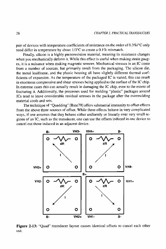
The technique of "Quadding" [Bate79] offers substantial immunity to offset effects from the above three sources of offset. While these effects behave in very complicated ways, if one assumes that they behave either uniformly or linearly over very small re- gions of an IC, such as the transducer, one can use the offsets induced in one device to cancel out those induced in an adjacent device.
VH3+
B- VH3- VH4+ B-
o JV - o
O O
o o ~ O O VH4-
B+
VH2- o o
O O
o o
O O
B- VH2+ VH1- B-
VHI+
Figure 2-13" "Quad" transducer layout causes identical offsets to cancel each other
out.
2.6. THE QUAD CELL 29
Figure 2-13 shows a Hall-effect transducer using a quadded layout. If one assumes that the effect causing the offset will create the offset equally in the four separate trans- ducers, then the AR will occur in the same physical leg of each device, and will result in a AV in addition to the Hall voltage from that device. The individual voltages seen at the outputs of the individual devices will be:
v. = v . + A v
= v . - A v
= v,, + A v
= v . - A v (Equation 2-3)
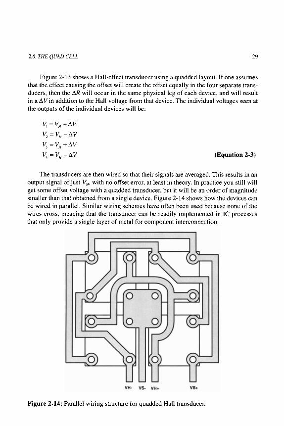
The transducers are then wired so that their signals are averaged. This results in an output signal of just Vn, with no offset error, at least in theory. In practice you still will get some offset voltage with a quadded transducer, but it will be an order of magnitude smaller than that obtained from a single device. Figure 2-14 shows how the devices can be wired in parallel. Similar wiring schemes have often been used because none of the wires cross, meaning that the transducer can be readily implemented in IC processes that only provide a single layer of metal for component interconnection.
U
0 0
0 0
VH- VS- VH+ VS+
Figure 2-14: Parallel wiring structure for quadded Hall transducer.

30 CHAPTER 2. PRACTICAL TRANSDUCERS
2.7 Variations on the Basic Hall-Effect Transducer
Although most commercial Hall-effect devices employ the types of transducers previ- ously described in this chapter, several variations on the basic technology have been developed that offer additional performance and capabilities. The two most significant of these technologies are the vertical Hall transducer and the incorporation of integrated flux concentrators.
One of the fundamental limitations of traditional Hall-effect transducers is that they provide sensitivity in only one axis--the one perpendicular to the surface of the IC on which they are fabricated. This means that to sense field components in more than one axis, one needs to use more than one sensor IC, and those sensor ICs must be in- dividually mounted and aligned. For example, in order to realize a three-axis magnetic sensor with traditional Hall-effect transducers, three separate devices must be used, and the designer must try to align them along the desired sensing axis, all while trying to maintain close physical proximity. While this is not impossible, it can be difficult and expensive to implement such a sensor, especially if the transducers need to be physi- cally close together.
The vertical Hall-effect transducer [Baltes94] is one means of providing multi-axis sensing capability on a single silicon die. Figure 2-15 shows the basic structure of this device.
SENSE- SENSE+
I I I I I --'="
p. , s
J
P+
MAGNETIC FIELD
Figure 2-15: Vertical Hall-effect transducer (after Baltes et al.).
ISOLATION RING

2.7. VARIATIONS ON THE BASIC HALL-EFFECT TRANSDUCER 31
In the vertical Hall-effect transducer, bias current is injected into an N-well from a central terminal 3, and is symmetrically collected by ground terminals 1 and 5. The current path goes down from the central terminal, and arches across the IC and back up to the ground terminals. In the absence of an applied magnetic field, this current distri- bution results in equal potentials being developed at sense terminals 2 and 4.
When a magnetic field is applied across the face of the chip perpendicular to the current paths, Lorentz forces cause a slight shift in the current paths, as they do in a tra- ditional Hall-effect transducer. This in turn causes a voltage differential to be developed across the sense terminals, which can then be amplified and subsequently processed into a usable signal level.
Because the vertical Hall-effect transducer, like its more traditional cousin, is sen- sitive to field in a single axis, it is possible to fabricate a two-axis sensor by placing a pair of these devices on a single silicon die by aligning their structures at 90 ~ rotation to each other. Finally, one can also add a conventional Hall-effect transducer to the same die to obtain a third axis of sensitivity. In this way, it becomes possible to create a three- axis magnetic transducer on a single silicon die.
One disadvantage of the vertical Hall structure is that it lacks four-way symmetry. As will be seen in the next chapter, transducer symmetry can be exploited at the system level to reduce the effects of ohmic offset voltage errors.
Another structure that offers significant advantages is the Hall-effect transducer with integrated magnetic f lux concentrators (IMCs) [Popovic01]. A magnetic flux con- centrator is a piece of ferrous material, such as steel, that is used to direct or intensify magnetic flux towards a sensing element. External flux concentrators have long been used externally to direct and concentrate magnetic flux in Hall-effect applications. The novel aspect of the IMC is in fabricating the flux concentrator on the surface of the sili- con die in extremely close proximity to the Hall-effect transducer, as shown in Figure 2-16.
Cell Y2
Bx ,~
Hall Cell II Cell X2
Y IY1
(a) (b)
Figure 2-16: Integrated magnetic flux concentrator, top view (a) and side view (b).
32 CHAPTER 2. PRACTICAL TRANSDUCERS
The flux concentrator shown in Figure 2-16 would normally be implemented as a thin layer of a high-permeability magnetic alloy such as permalloy (a nickel-iron steel), which would be laid down on the IC surface with an evaporation or sputtering process. In the configuration shown, there are four Hall-effect transducers arranged around the periphery of the flux concentrator. The concentrator performs two functions. The first is to concentrate the field in its proximity (Figure 2-16b). This intensifies the field seen by the transducers and has the effect of increasing the transducers' effective sensitivity. The second function performed by the concentrator is to redirect the axis of the applied field from horizontal to vertical near the transducers. For example, a hori- zontally applied X field is mapped into a positive Z component at transducer X 1 and a negative component at transducer X2. Note, however, that the transducers will still be sensitive to fields applied in the Z-axis despite the presence of the flux concentrator. By subtracting the outputs of the transducers (X2-X 1, Y2-Y 1), the effects of any Z-field components can be ignored. A microphotograph of an IMC Hall-effect transducer can be seen in Figure 2-17.
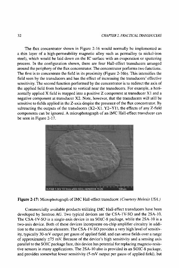
Figure 2-17: Microphotograph of IMC Hall-effect transducer. (Courtesy Melexis USA.)
Commercially available products utilizing IMC Hall-effect transducers have been developed by Sentron AG. Two typical devices are the CSA-1V-SO and the 2SA-10. The CSA-1V-SO is a single-axis device in an SOIC-8 package, while the 2SA-10 is a two-axis device. Both of these devices incorporate on-chip amplifier circuitry in addi- tion to the transducer elements. The CSA- 1 V-SO provides a very high level of sensitiv- ity, typically 30-mV output per gauss of applied field, and can sense fields over a range of approximately +75 mV. Because of the device's high sensitivity and a sensing axis parallel to the SOIC package face, this device has potential for replacing magneto-resis- tive sensors in many applications. The 2SA-10 also is provided in an SOIC-8 package, and provides somewhat lower sensitivity (5-mV output per gauss of applied field), but
2.8. EXAMPLES OF HALL EFFECT TRANSDUCERS 33
also offers two sensing axes, both parallel to the SOIC face. The primary application for this device is in sensing rotary position, where one simultaneously measures field strength in two axes, and resolves the two measurements into degrees of rotation.
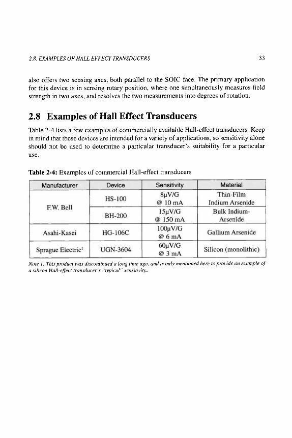
2.8 Examples of Hall Effect Transducers
Table 2-4 lists a few examples of commercially available Hall-effect transducers. Keep in mind that these devices are intended for a variety of applications, so sensitivity alone should not be used to determine a particular transducer's suitability for a particular use.
Table 2-4: Examples of commercial Hall-effect transducers
Manufacturer Device Sensitivity Material
EW. Bell
Asahi-Kasei
Sprague Electric ~
HS-100
BH-200
HG- 106C
UGN-3604
8IaV/G @ 10mA
151uV/G @ 150mA
1001uV/G @ 6 m A
601uV/G @ 3 m A
Thin-Film Indium Arsenide
Bulk Indium- Arsenide
Gallium Arsenide
Silicon (monolithic)
Note 1: This product was discontinued a long time ago, and is only mentioned here to provide an example of a silicon Hall-effect transducer's "typical" sensitivity..

This Page Intentionally Left Blank
Chapter 3
Transducer Interfacing
While it is possible to use a Hall-effect transducer as a magnetic measuring instrument with merely the addition of a stable power supply and a sensitive voltmeter, this is not a typical mode of application. More frequently the transducer is used in conjunction with electronics specially designed to properly bias it and perform some preprocessing of the resultant signals before presenting them to the end-user. The addition of applica- tion-specific electronics provides significant value by allowing the end-user to view the system as a black-box, without having to concern himself with the details of how the transducer is implemented. To differentiate a bare transducer from a transducer with support electronics, we will be referring to the latter as a sensor.
A minimal Hall-effect sensor (Figure 3-1) consists of three parts: a means of pow- ering or biasing the transducer, the transducer itself, and an amplification stage. Be- cause of the variety of applications in which Hall-effect sensors are employed, and their equally diverse functional requirements, there is no single "best way" to build even a minimal transducer interface. The "goodness" of any implementation is a function of how well it meets the requirements of a particular application. These requirements can include sensing accuracy, cost, packaging, power consumption, response time, and environmental compatibility. A $4,000 laboratory gaussmeter would not be a good (or even adequate) solution under the hood of a car, nor would a 20-cent commodity sen- sor IC be an especially good choice for many laboratory applications; each has its own application domain for which it is best suited.
35

36 CHAPTER 3. TRANSDUCER INTERFACING
IBIAS ,..~
Bias Circuit
Hall Transducer
>z _
I
Output Signal
Figure 3-1" Minimal components of Hall-effect sensor system.
3.1 An Electrical Transducer Model
To design good interface circuitry for a transducer requires that one understand how the transducer behaves. While the first two chapters described the physics and construction of a number of Hall-effect transducers, there still remains the question of how it behaves as a circuit element. Carrier concentration, current density, and geometry describe the device from a physical standpoint, but what is needed is a model that describes how the device interacts with transistors, resistors, op-amps, and other components dear to the hearts of analog designers.
When confronted with an exotic component, such as a transducer, a good circuit designer will attempt to build a model to approximately describe that device's behavior, as seen by the circuits it will be connected to. For this reason, the model will usually be built from primitive electronic elements, and be represented in a highly symbolic (schematic) manner. The elements employed can include resistors, capacitors, induc- tors, voltage sources and current sources. There are several advantages inherent in this approach:
1) Circuit designers think in terms of electronic components and a good circuit- level model can allow a designer to understand the system. A great model can give a circuit designer the gut-level intuitive understanding of the system needed to produce first-rate work. Alternatively, a poor model can give a cir- cuit designer gut-level feelings best resolved with antacids.
2) Simple circuit-level models often are analytically tractable. Deriving a set of closed-form analytic relationships can allow one to deliberately design to meet a set of goals and constraints, as opposed to designing through an itera- tive, generate-and-test procedure.

3.1. AN ELECTRICAL TRANSDUCER MODEL 37
3) Circuits can be automatically analyzed on a computer, by a number of com- mercially available circuit simulation programs (e.g., SPICE). In the hands of a skilled designer, the use of these tools can result in robust and effective designs. Conversely, in the hands of unskilled designers, their use can result in mediocre designs reached by trial-and-error (also known as the design by brute-force and ignorance method).
Figure 3-2 shows the model that was initially presented in the last chapter. It con- sists of four resistors and two controlled voltage sources. This model describes the transducer's input and output resistances, as well as its sensitivity as a function of bias voltage.
IVB+ /
RIN / 2
V = S*B*(VB.- V B.)/2 V = S*B*(VB+- V B.)/2
Rou T 12 l Rou T 12
< , ~ RIN / 2
1 Figure 3-2: Hall-effect transducer simple electrical model.
The four resistors describe the input and output resistances of the transducer. In the case of a transducer with four-way symmetry, all of the resistors are equal. The voltage sources model the transducer's sensitivity or the gain, which is a linear function of the bias voltage and the applied magnetic field, The various variables and constants in this model are defined as follows:

38 CHAPTER 3. TRANSDUCER INTERFACING
V~., VB_ Bias voltage S Sensitivity in Vo/B * Vi
B Magnetic flux density Rm Input resistance Rov.r Output resistance
Although this model is a gross simplification, it will exhibit enough of the electri- cal attributes of a transducer to be useful as an aid to designing interface circuits. The following are some of the major assumptions and limitations:
�9 Magnetic linearity; there are no saturation effects at high field. �9 Temperature coefficients are ignored. �9 There is no zero-flux offset. �9 The resistance as measured between adjacent terminals is unimportant for
many applications; modeling this correctly would unnecessarily complicate the model.
�9 A real Hall-effect sensor is a passive device; this model contains power-pro- ducing elements. We assume this additional power is small enough to ignore.
�9 The transducer is symmetric; the sense terminals are placed at the halfway point along the device.
3.2 A Model for Computer Simulation
The model presented in the last section can be adjusted so that it is suitable for simula- tion by SPICE (simulation program with integrated circuit emphasis) or another circuit simulation program. A few additional details need to be added both to make it more specific and to make it fit into SPICE's view of the world. Since SPICE doesn't directly handle magnetic field quantities, magnetic flux is represented by a voltage input to the model. SPICE also requires the user to define circuit topology by numbering each electrical node in the circuit. If you are using a graphical schematic-capture program to input your circuits, the computer numbers the nodes automatically. This can be a major convenience, especially when simulating large circuits. Figure 3-3 shows the SPICE- compatible circuit, with electrical nodes numbered.
The major adjustments to the model are to provide user control of an applied mag- netic field. This is what node 5 and resistor RB are for. When a connected circuit pres- ents a voltage to node 5, that voltage is interpreted as gauss input to the sensor. The resistor to ground is merely to guarantee that the node has a path to ground. This is done for reasons of numerical stability; it doesn't have any function in the circuit other than to make the circuit easier for SPICE to simulate.

3.2. A MODEL FOR COMPUTER SIMULATION 39
i
I
i
i
VOUT- D i
,,
Magnetic . Field Input D
,,
I
| ROUT2 EOUT2
|
RB
1E7
VBIAS+
. . . . . . . . . . . . . . . .
RIN1
EOUT1 A
IN2
. . . . . . . . . . . . . . . . . . . . . . . .
VBIAS-
VOUT+
Figure 3-3" Electrical model adapted for SPICE.
This schematic can now be translated into the SPICE language, and packaged as a subcircuit. Because of the number of commercial varieties of SPICE that have evolved over the past few years, we will be using a minimal set of features, so as to provide a least-common-denominator model. In keeping with this philosophy, the controlled sources (EOUT1 and EOUT2) are modeled as multidimensional polynomial functions of V5 and V l-V2. Some versions of SPICE will simply let you specify the source's gain algebraically (e.g., V(5) * (V(I)-V(2))) but this feature is not uniformly supported.
The subcircuit's user I/O ports are: Nodes 1, 2: bias connections (+ and - ) Nodes 3,4: output connections (+ and - ) Node 5: magnetic field input (1 gauss/Volt)
To finish this example and make this a complete model, we will use some of the parameters of the F.W. Bell BH-200 transducer:
�9 Sensitivity = 40 IJVo/G-V~n �9 R i n - 2.5E2 �9 R .... , = 2 ~
40 CHAPTER 3. TRANSDUCER INTERFACING
The resultant SPICE code is shown in Listing 3-1"
Listing 3-1" Simple SPICE model for BH200 Hall-effect transducer.
* EXAMPLE OF SIMPLE HALL-EFFECT TRANSDUCER MODEL FOR SPICE
.SUBCKT HALL1 (i 2 3 4 5)
* HALL EFFECT TRANSDUCER SUBCIRCUIT
* EACH RIN LEG HAS HALF OF 2.5 OHM INPUT RESISTANCE
RINI 1 6 1.25
RIN2 2 6 1.25
* EACH ROUT LEG HAS HALF OF 2 OHM OUTPUT RESISTANCE
ROUT1 7 3 1.00
ROUT2 8 4 1.00
* EACH SOURCE PROVIDES V5*(VI-V2)*GAIN/2
EOUTI 7 6 POLY(2) 5 0 1 2 0.0 0.0 0.0 0.0 20E-6
EOUT2 6 8 POLY(2) 5 0 1 2 0.0 0.0 0.0 0.0 20E-6
* LOAD FOR MAGNETIC INPUT (AS VOLTAGE) - KEEPS SPICE HAPPY
RB 5 0 IE7
.ENDS HALL1
**** TEST CIRCUIT ****
BIAS WITH 5V
VBIAS 1 0 5
* PROVIDE 1 MEG LOADS FROM OUTPUTS TO GND RLI 2 0 IE6 RL2 3 0 IE6
* DEFINE VMAG AS MAGNETIC FIELD INPUT
VMAG400
* CALL HALL TRANSDUCER SUBCIRCUIT
Xl 1 0 2 3 4 HALL1
* SWEEP MAGNETIC FIELD FROM -i000 TO +i000 GAUSS IN 20 G STEPS
* AND OUTPUT RESULTS
.DC VMAG -i000 i000 20
.PRINT DC V(4), V(2), V(3)
.PLOT DC V(4), V(2), V(3)
.END
This SPICE model provides the following features:
�9 Input and output resistance �9 A control for applied flux, via pin 5 �9 Output voltage, both as a function of bias voltage and applied field
To make for a simple illustration, we deliberately left a number of relatively use- ful features out of this model. Temperature coefficients of resistance and sensitivity,
3.3. VOLTAGE-MODE BIASING 41
for example, are not modeled in the above SPICE input file. SPICE is quite capable of simulating temperature-dependent behavior, provided one goes to the trouble to build an appropriate model. For many, if not most, purposes, however, the level of detail presented in this model will be sufficient for evaluating most of the circuits presented in this chapter. As with any computer model, your actual mileage may vary, depending on how you use (or abuse) it.
3.3 Voltage-Mode Biasing One of the major dichotomies in the design of a Hall-effect sensor is the mode in which the transducer is biased. It can be driven by either a constant voltage source or a con- stant current source; both modes have their advantages and their disadvantages. We will first look at circuitry for biasing a transducer with a constant-voltage source.
Buffer Amplifier
Voltage Reference
I
Hall Transducer
Output Signal
m
Figure 3-4" Voltage-mode Hall-effect sensor.
Figure 3-4 shows the basic arrangement of a voltage-biased Hall-effect sensor. There is a voltage reference, a buffer, the transducer, and an amplifier. One of the key features of this architecture is that, for most applications, the temperature coefficient of the transducer sensitivity will be sufficiently high that it must be compensated for. This can be done in one of two ways. The first is to make the voltage source temperature dependent so as to obtain a constant output level from the Hall-effect transducer. The second method is to make the gain of the amplifier temperature dependent, so it can compensate for the temperature-varying gain of the transducer signal. Although either method can be made to work, we will examine the case where the drive voltage is held constant over temperature.
A simple but workable bias circuit is shown in Figure 3-5a. A voltage reference, in this case a REF-02 type device, drives an op-amp follower to provide a stable voltage (+5V) to bias the Hall-effect transducer. When constructed from commonly available op- amps, such as the LM324 or TL081, this circuit can provide a few milliamperes of output drive, making it suitable for use with high input resistance transducers (Rin > 1 k,Q).

42 CHAPTER 3. TRANSDUCER INTERFACING
+15V
! REF-02 !
!
+15V (
.m
II
• -
m I
4- VHa l l
(a) (b)
Figure 3-5: Voltage bias circuits for low current (a) and high current (b) transducers.
Bulk and thin-film transducers, however, can often require as much as 100-200 mA for optimal performance. To bias these devices, the driver circuit of Figure 3-5b can be used. The addition of the transistor to the output of the op-amp increases its effective output current capability. When using this circuit, there are a few issues to keep in mind. First is whether or not the transistor has sufficient current gain (referred to as beta or 13). The maximum output current able to be drawn from the emitter of the transistor is limited to the maximum output current of the op-amp multiplied by the transistor's beta.
Another potential problem associated with this circuit is that of power dissipation in the transistor. For example, if the transducer draws 100 mA with only 0.2V of bias voltage, it only dissipates 20 mW. The drive transistor, however, if the collector is connected to a 5V supply, will dissipate nearly 500 mW of power. The maximum power dissipated in the transistor must be anticipated in the design, and should be a factor in selecting the transistor, as well as in determining what kind of additional heat-sinking is required, if any.
Finally, in either of the circuits of Figure 3-5, stability can become an issue, espe- cially if the transducer is operated at the end of a length of cable. The addition of para- sitic capacitance, or in some cases the additional transistor of Figure 3-5b, can cause the bias circuit to break out into oscillation. Because the stability of a given circuit is dependent on many variables, there is no simple one-size-fits-all fix. The circuit of Fig- ure 3-6 shows one approach that is often useful when driving loads at the end of long cables. This circuit works by providing separate feedback paths from the cable load and the output of the op-amp. The exact values required for the components (RF, CF, Ro) surrounding the op-amp will depend on the details of the application and the opamp chosen. For a general-purpose op-amp such as the TL081, setting RF to 100 kfL CF tO 100 pF, and Ro to 100f~ is a good starting point for experimentation in many cases.
43
§
IA. .
v
V REF ,,- Ro --4#v
I ii . D
3.1. AN ELECTRICAL TRANSDUCER MODEL
Figure 3-6: Circuit for driving capacitive loads.
All of the above bias circuits result in a small differential Hall output voltage riding on a fairly large common-mode voltage; specifically half the bias voltage. The com- mon-mode signal is the average of the two output voltages, while the differential is the difference. In the case of a Hall-effect transducer, the differential signal is the one carrying the measurement information. While it is possible to measure a small differ- ential signal riding on a large DC common-mode signal, signal recovery is easier if one doesn't have to deal with a large common-mode signal. The circuit of Figure 3-7 solves this problem by symmetrically biasing the transducer. If the transducer's sense termi- nals are halfway between the bias terminals, providing bias at +V a n d - V will result in zero common-mode output voltage. The Hall output voltage will in this case swing symmetrically about zero volts, for the case of ideally matched components. In reality this scheme will not completely eliminate common mode voltage from the transducer, but will reduce it to very low levels.
VREF
R A R §
VHALL
R
m
Figure 3-7" Symmetric bias circuit.
One problem frequently encountered when driving a Hall-effect transducer in con- stant-voltage mode is the voltage drops along long wires. This problem becomes espe- cially acute when the load requires a significant amount of current. While one solution

44 CHAPTER 3. TRANSDUCER INTERFACING
is to simply use thicker wires, this is not always either feasible or desirable. Another option is the use of a force-sense bias circuit. In a force-sense type of bias circuit, four wires are used to provide the bias voltage to the transducer. Two of the wires are used to provide positive supply and return (the force leads), while the remaining two (the sense leads) are used to measure the voltage that is actually being provided to the transducer. Because there is an insignificant amount of current flowing down the sense leads, there is no significant voltage drop along them, and they can be used to accurately measure the transducer bias voltage. Figure 3-8 shows a force-sense bias circuit using a dif- ferential amplifier (Gain = 1) to measure the voltage across the transducer. This circuit will impress VREe across the transducer bias terminals even if significant voltage drops (--1 V) occur along the force leads.
Opamp VREF
R1
Instrument
V+
Sense
R2
Force
+
VHALL
Figure 3-8: Force-sense bias circuit.
Resistors RI and R2 are in this circuit to handle the condition where one of the sense leads is accidentally disconnected. If this situation should occur, the differential amplifier will still measure the voltage applied to the force lead. This prevents the op- amp from overdriving and possibly damaging the transducer in the event of a broken sense connection.
It is also possible to construct a force-sense bias circuit with a single opamp, as shown in Figure 3-9. Good performance in this circuit, however, is highly dependent on the degree to which the values of all the RA resistors match each other.
Because force-sense techniques are normally employed when the transducer is some distance from the bias supply, stability again becomes an issue. The circuits of both Figures 3-8 and 3-9 would most likely require some modification in order to be successfully used in practice with commonly available op-amps and differential ampli- fiers.
3.4. CURRENT-MODE BIASING 45
VRE RA
RA m
I~ P
RA
V+
See
S . . . I
Er ce m
m
Figure 3-9: Force-sense circuit implemented with single op-amp.
3.4 Current-Mode Biasing Another way to bias a Hall-effect transducer is to feed it with a constant current; this mode of operation results in a Hall output voltage with a temperature coefficient on the order of 0.05%/~ as opposed to the 0.3%/~ obtained with constant-voltage biasing. For many applications, the tempco obtained with constant-current biasing is sufficient- ly low that no additional correction is necessary. An additional advantage is obtained when using long cable runs; because current does not "leak" out of wires to any ap- preciable degree under most circumstances, current-mode biasing doesn't normally re- quire any kind of force-sense arrangement to be used in the bias supply.
Voltage Source ' V ' Q
R
I ~ V / R
_
V H A L L
m y
m m
m I
Figure 3-10: Brute-force constant-current bias circuit.
46 CHAPTER 3. TRANSDUCER INTERFACING
There are a number of ways to construct constant-current bias sources for a Hall- effect transducer. The simplest method is to use a high-value resistor (R) in series with a constant voltage source, as shown in Figure 3-10. While such an arrangement is easy to make and inexpensive, maintaining a stable bias current requires that the voltage source be much greater than the transducer bias voltage. While this arrangement can be useful with bulk-type transducers that often operate with a bias voltage of under a volt, it can require excessively large voltage sources when used with integrated devices that may require several volts of bias.
The use of active electronics allows for the construction of stable current sources that don't require stable high voltage supplies. Figure 3-11 shows three common circuit topologies.
VREF V.
VREF
HALL VHALL
+ HALL
VREF
n D
(a) (b) (c)
:~ Rs
i 1
Figure 3-11: Constant current sources. Transistor (a) op-amp (b) op-amp with outboard transistor (c).
The circuit of Figure 3-11 a works by setting a voltage at the base of the transistor, approximately determined by V H = VkE~" RJ(RA + Rt~). This results in an emitter voltage about 0.6V lower, which then sets the current through Rs. The load (transducer) in the collector doesn't significantly affect the amount of current pulled through the collector, assuming that the collector voltage is higher than the emitter voltage so that the transis- tor is not saturated. The collector current is approximately given by:
Ic -- ~ R A + R~ (Equation 3-1)
This relation will hold substantially true if two conditions are met. The first is that the voltage across Rs is greater than 0.6V; this will minimize the effects of transistor VBE variation (VBE varies both over current and temperature, between individual transis- tors). The second condition is that (Rs" ~5) >> ((RA �9 R~)/(RA + R~)). If this condition is
3.4. CURRENT-MODE BIASING 47
violated the base will load down the RA/RH divider network and the output current may be significantly reduced.
The circuit in Figure 3-1 l b uses feedback to regulate current. By actively measur- ing the current passing through R s, and consequently through the transducer, the opamp can adjust its output voltage to obtain the desired current. The current is given simply by V~JRs , and if the op-amp has sufficient drive capabilities (current and voltage), the bias current will remain nearly constant over temperature. The output current drive capabilities of this circuit may be increased by adding a transistor to the output of the op-amp, in the manner similar to that shown previously in Figure 3-5b.
A third current source appears in Figure 3-1 1 c. This circuit adds the active feedback control of an op-amp to the circuit of Figure 3-1 l a. The resultant current is approxi- mately V~EflR s, with a small error (1-5%) resulting from base current feeding through the emitter and into the sense resistor. Adding feedback makes this circuit much less sensitive to variation in the transistor caused by both device-to-device differences and temperature effects, as compared to the circuit of Figure 3-II a.
One characteristic of all of the above circuits is that the transducer is "floating" with respect to ground, meaning that no terminal is grounded The transducer in Figures 3-11 a and 3-11 c is essentially "hanging" from the positive supply rail. The transducer of Figure 3-1 I b is floating at some indeterminate point in between ground and the posi- tive supply rail. A circuit called a Howland current source can be used to supply current to a ground-referenced load. Figure 3-12 shows the Howland current source.
RA
VREF Rs
R A R A
m m
+
VHALL
Figure 3-12- Howland current source.
m
To obtain good performance with a Howland current source, the RA resistors must be well matched and significantly greater in value than the sense resistor R s. The output current is given by VnEflRs.
48 CHAPTER 3. TRANSDUCER INTERFACING
3.5 Amplifiers With the transducer properly biased, one obtains a small differential voltage signal from the output terminals, often riding on a large DC common mode signal. The job of the amplifier is to amplify this small differential signal while rejecting the large common- mode signal. The fundamental circuit to perform this task is the differential amplifier (Figure 3-13), also known as an instrumentation amplifier (or in-amp).
. . - - - . . . . . VIN+ /
Gain='K' .~ VON. ~ --'- ~ V VOUT = K * (VoN+ "V 0N.)+VREF
F
Figure 3-13: Instrumentation amplifier.
A typical differential amplifier has a positive and a negative input terminal and an output terminal. The schematic symbol unfortunately looks a lot like that for an op-amp, sometimes leading to a bit of confusion. Some differential amplifiers have an additional reference input terminal, to which the output voltage is referenced. For most applications, this terminal will be tied to ground. Ideally, the output voltage is the dif- ference of the two input voltages. Because ideal devices are not yet available, you must make some trade-offs among various performance characteristics to get an amplifier that suits your needs. Some of the key parameters for differential amplifiers are:
�9 Differential Gain �9 Gain Stability �9 Input Offset Voltage �9 Input Bias Current �9 Common-Mode Rejection �9 Bandwidth �9 Noise
Differential gain is the gain by which the amplifier boosts the difference of the input signals. While there are monolithic instrumentation amplifiers that have fixed gains, this parameter is often user adjustable within wide limits, with ranges of 1000:1 commonly available.
Gain stability. One uses an instrumentation amp to get an accurate gain, and this is one of the features that differentiates them from the more common op-amp, which has a very large (>50,000) but not very well-controlled gain. Key gain-stability issues center around initial accuracy (% gain error) and stability over temperature (% drift/~

3.5. AMPLIFIERS 49
Input Offset Voltage. This is a small error voltage that is added to the differential input signal by the instrumentation amp. It results from manufacturing variations in the internal construction of the amplifier. The offset voltage is multiplied by the gain along with the signal of interest and can be a significant source of measurement error.
Input Bias Current. The inputs of the instrumentation amp will draw a small amount of input current. The amount is highly dependent on the technology used to implement the amplifier. Devices using bipolar transistors in their input stages tend to draw input currents in the range of nanoamperes, while those based on field-effect transistors (FETs) will tend to draw input bias currents in the picoampere or even fem- toampere ( 10 -~5) range. While FET-input instrumentation amps have lower bias currents than their bipolar counterparts, the input offset voltages are usually higher, meaning that a trade-off decision must be made to determine which technology to use for a given application.
Common-Mode Rejection. While the purpose of a differential amplifier is to am- plify just the difference between the input signals, it also passes through some of the common-mode, or average, component of the input signal. The ability of a given am- plifier to ignore the average of the two input signals is called the common mode rejec- tion ratio, or CMRR. It is defined as the ratio between the differential gain (Avd) and the common-mode gain (Ave) and, like many other things electrical, is often expressed logarithmically in decibels:
(Equation 3-2)
Common-mode rejection ratios of 80-120 dB (10,000-100,000) can be easily obtained by using monolithic instrumentation amplifiers. Additionally, the CMRR for many devices increases as the gain increases.
Bandwidth. Unless you are only interested in very slowly changing signals, you will probably be concerned with the frequency response, or bandwidth, of the ampli- fier. This is commonly specified in terms of a gain-bandwidth product (GBP). In rough terms, gain-bandwidth product can be defined as the product of the gain and the maxi- mum frequency at which you can achieve that gain. For many types of amplifiers, the GBP is roughly constant over a wide range of frequencies. For example, an amplifier with a I-MHz GBP can provide 1 MHz of bandwidth at a gain of 1, or conversely only 1000 Hz of bandwidth at a gain of 1000. Figure 3-14 shows how the gain of this hypo- thetical 1-MHz GBP amplifier varies when set at various gains.
One caveat, however, is that an amplifier doesn't simply block signals past its fre- quency response; the response gracefully degrades. For precision applications, you will want to choose your bandwidth so that it is at least a factor of 5-10 greater than that of the signal you are interested in. So, for the case of an amplifier with a gain of 1000 amplifying signals with useful information up to about 1000 Hz, you might want to use an instrument amplifier with a GBP of 5 to 10 MHz to preserve signal integrity.

50 CHAPTER 3. TRANSDUCER INTERFACING
AMPLIFIER GAIN
1000 (60dB)
100 (40 dB)
10 (20 dB)
1 (0 dB)
0.1 (-20dB)
~L
I I I I I w -
10Hz 100Hz lkHz 10kHz 100kHz 1MHz
FREQUENCY
Figure 3-14: Instrumentation amplifier frequency response vs. gain.
Noise. In addition to noise from the transducer, an amplifier will add some noise of its own. Although the sources of amplifier noise are complex and beyond the scope of this text, it can be modeled as a noiseless amplifier, with both voltage and current noise sources at the input, as shown in Figure 3-15. Because the noise from the current source is converted into voltage by the source impedance, it also ultimately appears as voltage noise. For a given input impedance Rs, the total amplifier noise is given by:
v~ =~(vN) 2 +(RsiN) 2 (Equation 3-3)
Noise is specified over a given bandwidth, and is usually given in terms of V~/Hz for voltage noise and amperesA/hertz for current noise. As with the case of transducer noise, the larger the bandwidth examined, the more noise that will be seen. (See Figure 3-15.)
Different technologies provide varying trade-offs between the magnitude of the voltage and current noise sources. Bipolar input amplifiers tend to have low voltage noise and high current noise, whereas amplifiers using FET technology tend to have higher voltage noise and lower current noise. The choice of technology is complex and is dictated by both the technical requirements and the economics of an application. As a general rule of thumb, however, bipolar-input amplifiers tend to give better noise per- formance with low impedance transducers (< 1 kf~) while FET-input devices contribute
3.6. AMPLIFIER CIRCUITS 51
less noise when used with higher impedance sources. Table 3-1 lists the voltage and noise parameters of a few commonly available op-amps.
a s
V n
Vo
Figure 3-15: Noise model of amplifier.
Table 3-1" Typical noise performance of various operational amplifiers at 1 kHz.
Device Technology VN (nV/VHz) IN (pN~JHz) OP27 Bipolar 3 1
OP42 JFET 13 0.007
TLC272 CMOS 25 Not avail.
3.6 Amplifier Circuits Although a number of techniques exist for constructing differential amplifiers, one of the simplest is to use an op-amp and a few discrete resistors as shown in Figure 3-16.
RA R B v. ~ V V ~ - - ~ ~ ~ ~ V ~ .
R A R a
V o
Figure 3-16: Differential amplifier.
This circuit provides an output voltage (with respect to ground) that is proportional to the difference in the input voltages. The output voltage is given by"

52 CHAPTER 3. TRANSDUCER INTERFACING
g B ( E q u a t i o n 3 -4 )
In the ideal case where the R A resistors match, the RR resistors match, and an "ide- al" op-amp is used, the common mode gain is zero. In the more realistic case where the resistors do not match exactly, the common mode gain is a function of the mismatch; the greater the mismatch, the higher the common mode gain and the less effective the differential amplifier will be at rejecting common mode input signal. For a differential amplifier constructed with 1% precision resistors, one can expect a CMRR on the order of 40-60 dB ( 100-1000).
One characteristic of this differential amplifier is that its input impedance is deter- mined by the R a and RB resistors. In situations where this circuit is used with a transduc- er with a comparable output impedance, severe gain errors can result from the amplifier loading down the transducer. One way around this problem is to buffer the inputs with unity-gain followers, as is shown in Figure 3-17a. This circuit can provide very high input impedances, especially when implemented with FET input op-amps.
vl. vl-
(a) (b)
Figure 3-17: Three-op-amp differential amplifiers. Simple buffered (a) classical (b).
Figure 3-17b shows the "Classical" three-op-amp instrument amplifier. In this cir- cuit, the input op-amps still provide high-impedance inputs, but they also provide an additional differential gain stage. The common mode gain of this first stage is unity, but the differential gain is given by:
2R o Avo = ~ + 1 ( E q u a t i o n 3 -5 )
Note that there is only one Rc in the circuit. Making this resistance variable allows for a single-point adjustment of the amplifier's gain.
With the addition of the final stage, the differential gain of the complete instrumen- tation amplifier is given by:
3.6. AMPLIFIER CIRCUITS 53
Avt~ -RR{2R~ j - R~- - ~ c +l (Equation 3-6)
The circuit of Figure 3-17b's use of two gain stages offers a number of significant advantages over the circuits of Figures 3-16 and 3-17a. First, it allows for the construc- tion of a higher-gain instrument amplifier for a given range of resistor ratios. Next, by splitting the gain across two stages, it offers higher frequency response for a given gain. Finally, because of the differential gain provided in the first stage, it becomes possible to build amplifiers with much higher levels of common-mode rejection, especially at higher gains.
While there are several other ways to obtain differential amplifiers, perhaps the easiest is to simply buy them; a number of manufacturers presently supply very high- quality devices at reasonable prices. One example of such a device is the AD627. Figure 3-18 shows how the device can be hooked up. Only one external component, a resistor (R(;) to set gain, is necessary for operation. As with any precision analog circuit, local power supply bypassing (in this case provided by capacitor C,) is usually a good idea.
o,
VIN
RG + 5 V
VouT
! ! CB
AD627 - - (S -p in D iP ) - -
Figure 3-18: External connections for AD627 monolithic instrumentation amplifier.
Aside from component count reduction, the use of monolithic devices offers many performance advantages. Some of the key parameters of the AD627 ("A" version for 5V operation at 25~ are listed in Table 3-2:
Table 3-2: Key parameters of AD627A instrumentation amplifier.
Parameter Min Typical Max Units Input offset voltage 50 250 IaV
Gain range 5 1000
Gain error (G=5) 0.03 0.10 %
(Continued)

54 CHAPTER 3. TRANSDUCER INTERFACING
Parameter Min Typical Max Units
Gain vs. temperature (G=5) 10 20 ppm/~
Input current 3 10 nA
Gain-bandwidth product 400 kHz
Common-mode rejection 77 90 dB
Input voltage noise (G= 100) 37 NV/~/Hz
Designing an instrumentation amplifier with this level of performance using dis- crete op-amps and resistors would be a challenging project, especially at a cost less than or equal to that of the AD627. For many applications, using an off-the-shelf monolithic instrumentation amplifier will be the most cost-effective means of achieving a desired level of performance.
3.7 Analog Temperature Compensation Although it is possible to make voltage sources, current sources, and amplifiers with a high degree of temperature stability, it is difficult to obtain this characteristic in a Hall-effect transducer. While the transducer provides a more constant gain over tem- perature when biased with a constant current (0.05%/~ than with a constant voltage (0.3%/~ many applications require higher levels of stability.
R T
Thermistor
R A
R B
Figure 3-19: Temperature-compensated amplifier.
Votrr
One method of increasing the temperature stability is to use an amplifier with a temperature dependent gain. Figure 3-19 shows one such implementation based on an op-amp and a thermistor, in an inverting configuration. As the temperature increases, the value of the thermistor decreases, causing the gain to rise. Because the temperature responses of most thermistors are highly nonlinear, it will often be impossible to obtain an exact desired gain-vs.-temperature response for any given combination of resistors and thermistors. The gain for this circuit as a function of temperature is given by:

3.7. ANALOG TEMPERATURE COMPENSATION 55
-Re (Equation 3-7) G (T)= RA + RT ( Y )
The best that can usually be done is to obtain an exact fit at two predetermined reference temperatures, with some degree of error at temperatures in-between. One procedure for designing this type of circuit, given a set of desired gains and a given thermistor, is as follows:
1) Determine the temperatures at which exact fit is desired (T,, 7"2) 2) Determine the gain at T, and 7"2 (G,, G2) 3) Determine the resistance of the thermistor at T,, 7"2 (Rr~, Rrz) 4) Calculate R a by:
(G2RT2 - G1R r ) R a = ' (Equation 3-8)
G, - G 2
5) Calculate Re by:
R, = -G, ( e A -~ RT, ) (Equation 3-9)
The above procedure assumes that a positive temperature coefficient of gain is desired and the resistor has a negative temperature coefficient. Note that there will be some cases for which a viable solution doesn't exist (usually indicated by a negative value for RA or R~), and others for which the solution may be unacceptable (i.e., resistor values are too low or too high).
Example: Design a circuit to provide a gain o f - 9 at 0~ and -11 at 50~ The thermistor to be used has a resistance of 32.65 kf~ at 0~ and 3.60 k ~ at 50~ (As a side note, this degree of resistance variation is not at all unusual in a thermistor; the device
used in this example is a 10-kf~ (nominal @ 25~ "J" curve device.)
G l = ~9
G 2 = - 1 1
RT, = 32.65 ks
RT2 = 3.60 kf~
g A =
(Equation 3-10)
(G2RT2 -- GIRT, ) ( - l l . 3.60 kf~ - ( - 9 * 32.65 kf~)) = = 127 kf~
(GI - G 2 ) ( - 9 - ( - 1 1 ) )
56 CHAPTER 3. TRANSDUCER INTERFACING
R B = - G , (R A + R,., )= - ( -9 ) (127 kf2 + 32.65 kf~)= 1436 kf2 (Equation 3-11)
Table 3-3 shows the gain of this circuit for several temperatures, and the departure from a straight-line fit (% error).
Table 3-3: Temperature compensated amplifier performance.
T RT Ideal Gain Actual Gain Error (~ (k.Q) (straight-line) (circuit) % -20 97.08 -8.2 -6.4 22
-10 55.33 -8.6 7.9 8
0 32.65 -9 -9 0
10 19.90 -9.4 -9.8 4
20 12.49 -9.8 10.3 5
30 8.06 10.2 -10.6 4
40 5.33 10.6 -10.8 2
50 3.60 11 11 0
60 2.49 11.4 -11.1 -3
70 1.75 11.8 -11.2 -5
Although temperature-compensated amplifiers can be useful in certain situations, they suffer from two principal drawbacks. The first is that, as the above example shows, it can be difficult to get the curve one really wants with available components. Although various series and parallel combinations of resistors and thermistors can be used to get more desirable temperature characteristics (with varying degrees of success), this also results in more complex design procedures, with the design process often deteriorating into trial-and-error.
The second drawback is a little more philosophical; the underlying physical mech- anism responsible for transducer gain variation will rarely be the same as that underly- ing the temperature response of your compensated amplifier. In practice this means that you often can't design a compensation scheme that works well over the process variation seen in production. Any given compensation scheme may need to be adjusted on an individual basis for each transducer, or at least on a lot-by-lot basis in production. Since this adjustment process requires collection of data over temperature, it can be an expensive proposition with lots of room for error.
3.8. OFFSET ADJUSTMENT 57
3.8 Offset Adjustment While some systematic attempts can be made to temperature compensate the gain of a Hall-effect transducer, the ohmic offset voltage is usually random enough so that to make any significant reduction requires compensation of devices on an individual basis. Moreover, since the drift of the ohmic offset will also usually have an unpredict- able component, one will often only try to null it out at a single temperature (such as 25 ~
The simplest method of offset adjustment is shown in Figure 3-20; it uses a manual potentiometer to null out the offset of the Hall-effect transducer. The potentiometer is used to set a voltage either positive or negative with respect to the output sense termi- nal, and a high-value resistor (RA) sets an offset current into or out of the transducer. It is therefore possible to null out either positive or negative offsets with this scheme.
VBIAS+
VmAS-
~(~)Offset Adjust
. . ._ v +
VHALL
Figure 3-20- Manual offset adjustment using potentiometer.
An adjustment made in this manner is relatively stable over temperature, particu- larly if the temperature coefficient of resistance of RA can be made similar to that of the transducer output. Another feature of this trim method is that it can be used regardless of whether the transducer is biased from a constant current or a constant voltage source. The amount of trim current injected through R a will be proportional to the bias voltage, and will thus track the transducer's ohmic offset over variations in bias voltage.
Offset adjustment can also be made at the amplifier. When performing offset cor- rection in the amplifier circuitry, an important consideration is that the transducer's off- set voltage will be proportional to the voltage across its drive terminals. The input offset voltage of the amplifier, however, will be independent of sensor bias conditions. In the case of a transducer being operated from a constant bias voltage, both offsets can be approximately corrected through one adjustment. Because Hall-effect transducers are
58 CHAPTER 3. TRANSDUCER INTERFACING
more typically biased with a constant current source, the transducer bias voltage will change as a function of temperature. There are several approaches to dealing with these two independent offset error sources. The first is to get an amplifier with an acceptably low input offset specification and simply ignore its input offset voltage. A circuit to perform an adjustment of transducer offset is shown in Figure 3-21. This circuit mea- sures the actual bias voltage across the transducer and generates proportional positive and negative voltage references based on the bias voltage. The potentiomcter allows one to add an offset correction to the amplified sensor signal. Since this correction will be proportional to the transducer bias voltage, it will track changes in transducer offset resulting from bias variation over temperature.
If a separate offset adjustment were added to correct for input voltage offset of the instrumentation amplifier, the offset adjustment process would need to be performed as a two-stage process. First the amplifier inputs would need to be shorted together and the amplifier offset adjusted, for zero output voltage. Next, the short would be removed, and the Hall-offset adjust would be used to trim out the remaining offset.
+VBIAS
RA Offset Adjust e
ImAS "'_t_ L".
~ r Ro
Rc
Votrr
Figure 3-21" Correcting transducer offset at the amplifier.
3.9 Dynamic Offset Cancellation Technique In addition to removing zero-flux ohmic offset by manually trimming it out, an elegant method exists that exploits a property of the Hall-effect transducer to reduce system offset.
A four-way symmetric Hall-effect transducer can be viewed as a Wheatstone bridge. Ohmic offsets can be represented as a small AR, as shown in Figure 3-22a. When bias cur- rent is applied to the drive terminals, the output voltage appearing at the sense terminals is V, + VE, where VH is the Hall voltage and VE is the offset error voltage.
3.9. DYNAMIC OFFSET CANCELLATION TECHNIQUE 59
IBIAS
IBIAS
AR
(a)
4- VH4-V
(b)
4-
V H 4-V E
Figure 3-22: Effects of rotating bias and sense terminals on output.
Now consider what happens if we take the transducer and reconnect the bias and sense terminals, as shown in Figure 3-22b. All of the terminal functions have been ro- tated clockwise by 90". The sense terminals are now connected to bias voltage, and the former drive terminals are now used as outputs. Because the transducer is symmetric with rotation, we should expect to see, and do see, the same Hall output voltage.
The transducer, however, is not symmetric with respect to the location of AR. In effect, this resistor has moved from the lower right leg of the Wheatstone bridge to the upper right leg, resulting in a polarity inversion of the ohmic offset voltage. The total output voltage is now V , - V~:. One way to visualize this effect is to see the Hall volt- age as rotating in the same direction as the rotation in the bias current, while the ohmic offset rotates in the opposite direction.
If one were to take these two measurements to obtain V, + V~: and VII-V~:, one can then simply average them to obtain the true value of V,. For this technique to work, the only requirement on the Hall-effect transducer is that it be symmetric with respect to rotation.
It is possible to build a circuit that is able to perform this "plate-switching" func- tion automatically. By using CMOS switches, one can construct a circuit that can rotate the bias and measurement connections automatically. Such a circuit is shown in Figure 3-23. An oscillator provides a timing signal that controls the switching. When the clock output is LOW, the switches A,B,E, and F close, and switches C,D,G, and H open. This places the transducer in a configuration that outputs V, + V~:. When the clock goes HIGH, switches C,D,G,H close, while the remaining switches open. This outputs V , - VE.
60 CHAPTER 3. TRANSDUCER INTERFACING
CLOCK
t J= _ ,..,I= 1
~ D ~'~ ~ /'~ E ~
B H
~ ~ ~ ' - ~ VF
i
Figure 3-23: Switching network and output filter for auto-nulling offset voltage.
The output signal produced by the transducer and this periodic switching network next needs to be amplified and averaged. While there are several ways of averaging the signal over time, the simplest is through the use of a low-pass filter. Examples of signals present at various stages of this network are shown in Figure 3-24.
CLOCK I I I I I I
Vo
V F (FILTERED OUTPUT)
VH'I'V E
VH'V E
. . . . . . . . . . . . . . . . . . . . . . . . . . . . . . . . . . . . . . . . . . . . . . . . . . . . . v H
Figure 3-24: Auto-nulling circuit waveforms.
This technique is used, with suitable modifications, in many modem Hall-effect integrated circuits. It is often referred to by the terms plate-switching, auto-nulling, and chopper-stabilization. When properly implemented, it can reduce the effective ohmic offset of a given transducer by nearly two orders of magnitude. Additionally, since the offset is being cancelled out dynamically, it is very temperature stable. This technique can also be employed in the construction of the digital-output Hall-effect ICs, result- ing in highly sensitive devices with low and temperature-stable operate (turn-on) and release (turn-off) points.
Related Documents