PERTUNJUKAN LASER DIGITAL TUGAS AKHIR Diajukan untuk memenuhi salah satu syarat memperoleh gelar Sarjana Teknik Program Studi Teknik Elektro Disusun oleh: LEO AGUNG CAHYONO NIM: 005114036 JURUSAN TEKNIK ELEKTRO FAKULTAS TEKNIK UNIVERSITAS SANATA DHARMA YOGYAKARTA 2007

Welcome message from author
This document is posted to help you gain knowledge. Please leave a comment to let me know what you think about it! Share it to your friends and learn new things together.
Transcript

PERTUNJUKAN LASER DIGITAL
TUGAS AKHIR
Diajukan untuk memenuhi salah satu syarat memperoleh gelar Sarjana Teknik
Program Studi Teknik Elektro
Disusun oleh:
LEO AGUNG CAHYONO
NIM: 005114036
JURUSAN TEKNIK ELEKTRO
FAKULTAS TEKNIK
UNIVERSITAS SANATA DHARMA
YOGYAKARTA
2007

DIGITAL LASER SHOW
FINAL PROJECT
Presented as partial fulfillment of the requirements to obtain The Sarjana Teknik Degree
In Electrical Engineering Study Program
By:
LEO AGUNG CAHYONO
NIM: 005114036
ELECTRICAL ENGINEERING DEPARTMENT
ENGINEERING FACULTY
SANATA DHARMA UNIVERSITY
YOGYAKARTA
2007


HALAMAN PERSEMBAHAN
+Tftfpsboh!ujebl!ejojmbj!ebsj!tfcfsbqb!ujohhj!ejb!nfmpnqbu-!ubqj!ebsj!
tfcfsbqb!ujohhj!ejb!nfmfoujoh!lfncbmj!tfufmbi!ejb!kbuvi+!
“Setiap kejadian dalam hidup adalah takdir dan kita tidak dapat merubahnya. Namun,
bagaimana kita menyikapinya merupakan pilihan bebas kita. Dan pilihan bebas kita itulah yang
akan menentukan takdir kita selanjutnya”
“Cinta itu putih, namun jangan pernah lupa bahwa putih itu
sebenarnya mejikuhibiniu”
Skripsi ini kupersembahkan untuk:
Baba⁄
Bapak, Ibu, dan Adikku⁄
Teman-teman⁄
Siapa saja⁄
vi

KATA PENGANTAR
Puji syukur sebesar-besarnya penulis panjatkan kepada Tuhan Yang Maha
Esa, atas berkah, rahmat, cobaan dan masalah, kesulitan, serta kasih-Nya yang
dilimpahkan kepada penulis, sehingga penulis dapat menyelesaikan skripsi ini dengan
baik.
Penulisan skripsi ini merupakan salah satu syarat untuk menyelesaikan studi
penulis dan untuk memperoleh gelar Sarjana Teknik Program Studi Teknik Elektro di
Universitas Sanata Dharma. Penulisan skripsi ini didasarkan pada hasil-hasil yang
penulis peroleh mulai dari perancangan, pembuatan alat sampai pada pengujian alat
yang, juga kemungkinan pengembangannya.
Dengan selesainya Tugas Akhir yang memberikan banyak sekali pembelajaran
dan pengembangan bagi penulis baik dari segi teknis maupun personalitas ini, maka
penulis ingin menyampaikan rasa terima kasih yang sebesar-besarnya kepada:
1. Shrii Shrii Ananda Murtii, as the lovely Baba. Thanks for everything, Baba.
2. Pak Djoko selaku pembimbing I, sekaligus sebagai mentor, dan motivator
yang selalu menemani dan memberikan semangat, serta tidak pernah marah
ataupun kesal walaupun penulis sering “menghilang”.
3. Pak Tjendro, selaku pembimbing II, yang selalu tersenyum dan penuh
pengertian.
4. Para dosen, staf administrasi, serta laboran yang telah banyak memberikan
ilmu pengetahuan, bimbingan, serta kesempatan untuk studi dan juga
menyelesaikannya dengan baik.
5. Bapak, Ibu, Tante Niek, Om Dikin dan Adikku Yus, yang selalu mencintai,
mendukung dan mendoakanku.
6. Rekan-rekan di teknik elektro: Teguh, Wayan, Andan, Titus, Poer, BK, BT,
Stephen, Dewi, Tika, Wahyu, Supri, Bram dan teman-teman lainnya yang
selalu menemani dan memberi masukan serta semangat dalam perjuangan ini.
7. Rekan-rekan di AMURT: Dada Shiila, Paunkaj, Dada Satya, Dada Ratnesh,
Didi Vitaraga, “mother” Amrta, Ista, mbak Sita dan mas Taufik, Mahadeva,
mas Suman, Aravinda, Prabha, dan Baskar atas dukungan, kasih, dan
pengertiannya selama ini. Terus berjuang teman-teman.
8. Serta berbagai pihak yang tidak bisa disebutkan satu persatu di sini.
vii

Penulis menyadari bahwa dalam karya tulis ini masih terdapat banyak
kekurangan dan masih jauh dari sempurna. Oleh akrena itu segala bentuk masukan,
baik berupa kritik maupun saran yang membangun sangat penulis harapkan dari
pembaca, demi perbaikan dan kesempurnaan skripsi ini.
Terima kasih Tuhan.
Yogyakarta, 27 Maret 2007
Penulis
viii

PERTUNJUKAN LASER DIGITAL
Disusun oleh: Leo Agung Cahyono
005114036
INTISARI Sinar laser telah digunakan secara luas dalam berbagai bidang kehidupan, seperti: medis, teknologi elektronika dan komunikasi, militer, serta hiburan. Sebagai sarana hiburan, sinar laser dapat digunakan untuk membangkitkan pola-pola geometris tertentu dengan cara memantulkannya ke sebuah atau beberapa cermin yang diputar dengan kecepatan dan arah putaran tertentu. Dalam penelitian ini, digunakan dua buah motor DC untuk memutar cermin yang akan digunakan sebagai sasaran pantulan sinar laser. Untuk mengendalikan kecepatan motor digunakan suatu metode pengendalian tegangan yang disebut PWM (Pulse Width Modulation). PWM dihasilkan oleh perangkat mikrokontroler AT89S51 dengan derajat kenaikan duty cycle sebesar 1%. Untuk dapat menghasilkan putaran yang dapat berputar ke dua arah, baik searah maupun berlawanan jarum jam, digunakan driver berupa jembatan H, yang terintegrasi dalam IC L293D. Masukan untuk pengendalian kecepatan dan arah tersebut dapat dilakukan melalui tombol push-button ataupun menggunakan remote control. Pola-pola yang dihasilkan pada penelitian ini menunjukkan bahwa bentuk dan arah gerakan pola-pola tersebut ditentukan oleh kecepatan dan arah putar cermin pemantulnya. Kata kunci : Laser, PWM, remote control, jembatan H, motor DC
ix
DIGITAL LASER SHOW
By: Leo Agung Cahyono
005114036
ABSTRACT Laser has been widely use in many fields, such as: medic, communication and electronic technology, military and also entertainment. As an entertainment tool, laser can be used to generate several geometrical patterns by reflecting it to one or some mirrors which is rotated with a particular speed and direction. In this research, two DC motors are used to rotate two mirrors which are going to be used as a target of the laser reflection. To controlled the speed of the motors, a voltage-controlling methoed called Pulse Width Modulation (PWM) is implemented. The PWM is generated with 1% duty cycle increment or decrement by AT89S51 microcontroller. To obtain a rotation which can turn in two directions, clock and counter clock wise, an H-Bridge driver which is integrated in L293D driver is used. The inputs to control the speed and direction use push-button and remote control. The patterns that are generated in this research show that the shapes and the movement directions of those patterns are determined by the speed and the rotation direction of the reflecting mirrors. Keywords : Laser, PWM, remote control, H-Bridge, DC Motors
x
DAFTAR ISI
Halaman Judul ........................................................................................................... i
Halaman Persetujuan ................................................................................................. iii
Halaman Pengesahan ................................................................................................. iv
Halaman Pernyatan Keaslian Karya .......................................................................... v
Halaman Persembahan............................................................................................... vi
Kata Pengantar ........................................................................................................... vii
Intisari ....................................................................................................................... ix
Abstract ...................................................................................................................... x
Daftar Isi .................................................................................................................... xi
Daftar Gambar ........................................................................................................... xiv
Daftar Tabel ............................................................................................................... xvi
Daftar Lampiran......................................................................................................... xvii
BAB I. PENDAHULUAN
1.1. Latar Belakang Masalah ................................................................................. 1
1.2. Perumusan Masalah ........................................................................................ 1
1.3. Pembatasan Masalah....................................................................................... 1
1.4. Tujuan dan Manfaat Penelitian ....................................................................... 2
1.5. Metodologi Penelitian..................................................................................... 2
1.6. Sistematika Penulisan ..................................................................................... 3
BAB II. DASAR TEORI
2.1. Pola-Pola Dasar Hasil Tampilan Perangkat Laser Show................................ 4
2.2. Kurva Lissajous .............................................................................................. 5
2.3. Hypotrochoid .................................................................................................. 6
2.3.1. Hypocycloid........................................................................................... 7
2.3.2. Rose........................................................................................................ 9
2.4. Laser .............................................................................................................. 10
2.5. Keunggulan Utama Laser .............................................................................. 11
2.6. Mikrokontroler AT89S51 ............................................................................... 12
2.6.1. Pengenalan Mikrokontroler ................................................................... 12
xi

2.6.2. Struktur Memori..................................................................................... 12
2.6.2.1. RAM Internal ................................................................................ 13
2.6.2.2. Special Function Register ............................................................. 14
2.6.2.3. Flash PEROM ............................................................................... 14
2.6.3. Timer...................................................................................................... 14
2.6.3.1. Timer Untuk Menghasilkan Tunda Waktu .................................. 16
2.6.3.2. Tunda Waktu Menggunakan Looping ......................................... 16
2.6.4. Interupsi ................................................................................................. 17
2.7. Rangkaian Single Chip Mikrokontroler ......................................................... 19
2.8. Remote Control ............................................................................................... 20
2.8.1. Remote Control Sony............................................................................. 21
2.8.2. IR Receiver Module............................................................................... 22
2.9. Motor DC ....................................................................................................... 22
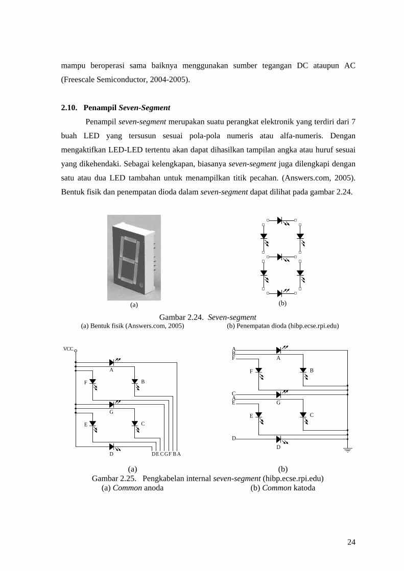
2.10. Penampil Seven-Segment ............................................................................. 24
2.11. Pulse Width Modulation ............................................................................... 25
2.12. Transistor Sebagai Saklar ............................................................................. 26
2.12.1. Kondisi Cuf-off .................................................................................... 27
2.12.2. Kondisi Saturasi ................................................................................... 27
2.13. H-Bridge ....................................................................................................... 28
BAB III. PERANCANGAN
3.1. Diagram Kotak Laser Digital.......................................................................... 31
3.2. Konstruksi Dasar Digital Laser Show............................................................. 33
3.3. Input Interface................................................................................................. 35
3.3.1. Pengontrolan Menggunakan Tombol Push-Button................................ 35
3.3.2. Pengontrolan Secara Nirkabel Menggunakan Remote Control ............. 36
3.4. Driver Motor DC............................................................................................. 37
3.5. Tampilan Seven-Segment ............................................................................... 39
3.6. Perancangan Perangkat Lunak........................................................................ 41
3.6.1. Diagram Alir Utama .............................................................................. 41
3.6.2. Diagram alir Proses Inisilasisasi Utama ................................................ 42
3.6.3. Interupsi Generator PWM...................................................................... 42
3.6.4. Diagram Alir Interupsi Penekanan Tombol ........................................... 43
3.6.4.1. Diagram Alir Subrutin Tunda Untuk Mengatasi Efek Bouncing . 45
xii

3.6.4.2. Diagram Alir Subrutin Pengubahan Arah Motor.......................... 46
3.6.5. Diagram Alir Pendeteksian Remote Control ......................................... 47
3.6.5.1. Diagram Alir Subrutin Tunda 2,45 mS......................................... 51
3.6.6. Interupsi Scanning 7-Segment ............................................................... 52
3.6.6.1. Diagram alir Subrutin Pengubahan Data dari Heksa Desimal
Menjadi BCD................................................................................ 53
BAB IV. PENGAMATAN DAN PEMBAHASAN
4.1. Pengamatan Terhadap Sinyal Keluaran IR Receiver Module ........................ 56
4.2. Pengamatan Terhadap Pulsa PWM................................................................. 57
4.3. Hubungan kecepatan motor dengan presentase PWM.................................... 59
4.4. Hubungan PWM, kecepatan motor, dan pola yang dihasilkan....................... 64
4.5. Bentuk fisik alat .............................................................................................. 66
4.6. Penempatan mekanis motor, cermin, dan laser............................................... 67
BAB V. KESIMPULAN DAN SARAN
5.1. Kesimpulan .................................................................................................... 69
5.2. Saran .............................................................................................................. 69
Daftar Pustaka .............................................................................................................. 70
Lampiran
xiii
DAFTAR GAMBAR
Gambar 2.1. Prinsip dasar operasi laser show ......................................................... 4
Gambar 2.2. Pola dasar hasil tampilan laser show................................................... 5
Gambar 2.3. Beberapa contoh kurva Lissajous ...................................................... 6
Gambar 2.4. Ilustrasi definisi hypotrochoid ............................................................ 6
Gambar 2.5. Ilustrasi definisi hypocycloid ............................................................. 7
Gambar 2.6. Hypocycloid dengan n berupa bilangan integer ................................. 8
Gambar 2.7. Hypocycloid dengan a/b berupa bilangan rasional ............................ 8
Gambar 2.8. Hypocycloid dengan a/b berupa bilangan irrasional .......................... 8
Gambar 2.9. Rose dengan n berupa bilangan ganjil dan genap .............................. 9
Gambar 2.10. Rose dengan n berupa bilangan rasional ............................................ 9
Gambar 2.11. Rose dengan n berupa bilangan irrasional .......................................... 10
Gambar 2.12. Alamat RAM internal dan Flash PEROM .......................................... 13
Gambar 2.13. Register TMOD................................................................................... 14
Gambar 2.14. Register TCON ................................................................................... 16
Gambar 2.15. Register IE........................................................................................... 18
Gambar 2.16. Sumber interupsi ................................................................................. 18
Gambar 2.17. Rangkaian single chip microcontroller ............................................... 19
Gambar 2.18. Rangkaian reset secara manual ........................................................... 20
Gambar 2.19. Pemodulasian sinyal infra merah ........................................................ 21
Gambar 2.20. Pengkodean lebar pulsa SIRC Sony.................................................... 21
Gambar 2.21. Protokol SIRC Sony............................................................................ 22
Gambar 2.22. Diagram blok receiver infra merah..................................................... 22
Gambar 2.23. Prinsip kerja motor DC ....................................................................... 23
Gambar 2.24. Seven-segment .................................................................................... 24
Gambar 2.25. Pengkabelan internal seven-segment .................................................. 24
Gambar 2.26. Sinyal PWM dengan duty cycle bervariasi ......................................... 26
Gambar 2.27. Transistor NPN sebagai saklar pada kondisi ideal versi electron flow 26
Gambar 2.28. Transistor PNP sebagai saklar pada kondisi ideal versi electron flow 28
Gambar 2.29. Rangkaian dasar sebuah H-bridge....................................................... 28
Gambar 2.30. Diagram internal IC L293D ................................................................ 29
Gambar 3.1. Diagram kotak digital laser show........................................................ 32
xiv

Gambar 3.2. Layout digital laser show .................................................................... 34
Gambar 3.3. Rangkaian antara push-button dengan mikrokontroler ....................... 35
Gambar 3.4. Rangkaian antara IR Receiver dengan mikrokontroler....................... 37
Gambar 3.5. Rangkaian driver motor DC................................................................ 37
Gambar 3.6. Rangkaian seven-segment................................................................... 39
Gambar 3.7. Diagram alir utama.............................................................................. 41
Gambar 3.8. Diagram alir inisialisasi mikrokontroler ............................................. 42
Gambar 3.9. Diagram alir interupsi timer 1: PWM ................................................. 43
Gambar 3.10. Diagram alir interupsi penekanan tombol ........................................... 44
Gambar 3.11. Diagram alir subrutin tunda bouncing ................................................ 45
Gambar 3.12. Diagram alir subrutin tunggu tombol dilepas ..................................... 46
Gambar 3.13. Diagram alir interupsi pendeteksian remote control ........................... 48
Gambar 3.14. Diagram alir subrutin tunda 2,45 mS .................................................. 51
Gambar 3.15. Diagram alir tampilan seven-segment................................................. 52
Gambar 3.16. Diagram alir subrutin pengubahan data dari heksa decimal menjadi
BCD .................................................................................................... 54
Gambar 3.17. Diagram alir subrutin pengecekan dan pengubahan nibble ................ 55
Gambar 4.1. Sinyal keluaran IR Receiver module .................................................. 56
Gambar 4.2. Bentuk pulsa PWM dengan duty cycle 63%....................................... 57
Gambar 4.3. Hubungan kecepatan putar searah jarum jam (CW) motor 1 terhadap
presentase PWM ................................................................................ 60
Gambar 4.4. Hubungan kecepatan putar berlawanan jarum jam (CCW) motor 1
terhadap presentase PWM.................................................................. 61
Gambar 4.5. Hubungan kecepatan putar searah jarum jam (CW) motor 2 terhadap
presentase PWM ................................................................................ 60
Gambar 4.6. Hubungan kecepatan putar berlawanan jarum jam (CCW) motor 2
terhadap presentase PWM.................................................................. 60
Gambar 4.7. Bentuk fisik alat .................................................................................. 66
Gambar 4.8. Penempatan mekanis motor, cermin, dan laser................................... 67
xv

DAFTAR TABEL
Tabel 2.1. Jenis-jenis laser besera panjng gelombang dan penggunaannya .............. 10
Tabel 2.2. Mode kerja timer....................................................................................... 15
Tabel 2.3. Tabel kebenaran IC L293D....................................................................... 30
Tabel 3.1. Arah putaran motor DC ............................................................................ 38
Tabel 3.2. Interupsi yang digunakan pada program Digital Laser Show................... 41
Tabel 3.3. Perancangan fungsi dari tombol remote control yang ditekan ................. 50
Tabel 4.1. Fungsi dari tombol remote control yang ditekan ...................................... 57
Tabel 4.2. Data pengamatan duty cycle PWM .......................................................... 58
Tabel 4.3. Kecepatan motor 1 saat berputar searah jarum jam (CW)........................ 60
Tabel 4.4. Kecepatan motor 1 saat berputar berlawanan jarum jam (CCW)............. 61
Tabel 4.5. Kecepatan motor 2 saat berputar searah jarum jam (CW)........................ 62
Tabel 4.6. Kecepatan motor 2 saat berputar berlawanan jarum jam (CCW)............. 63
Tabel 4.7. Pola yang terbentuk saat kedua motor berputar searah............................. 64
Tabel 4.8. Pola yang terbentuk saat kedua motor berputar berlawanan arah............. 65
xvi

DAFTAR LAMPIRAN
Lampiran I Rangkaian Digital Laser Show
Lampiran II Source code program Digital Laser Show
Lampiran III Kode tombol remote control SONY RM-687C
Lampiran IV Datasheet mikrokontroler Atmel AT89S51
Lampiran V Datasheet IC L293D
Lampiran VI Datasheet Transistor BC516
Lampiran VII Datasheet Seven-segment MAN5750
xvii

BAB I
PENDAHULUAN
1.1. Latar Belakang
Sejak pertama kali berhasil diujicobakan pada tahun 1960 oleh fisikawan
Amerika Serikat, Theodore Harold Maiman (Microsoft, 2005), teknologi dan aplikasi
laser terus berkembang dengan pesat. Hal ini mengakibatkan berbagai bidang yang
mengaplikasikan laser dalam sistemnya seperti medis, teknologi elektronika dan
komunikasi, militer, serta hiburan juga mendapat berbagai kemajuan yang cukup
berarti.
Dalam bidang hiburan, laser digunakan untuk mendapatkan efek-efek visual
yang biasanya mengiringi sebuah pertunjukan kembang api. Efek-efek sinar laser
telah memancing rasa keingintahuan banyak orang tentang apa sebenarnya sinar laser
itu dan bagaimana caranya menghasilkan pola-pola yang indah tersebut.
Seperangkat alat profesional akan menjadi terlalu berlebihan apabila hanya
akan digunakan untuk memuaskan rasa keingintahuan tersebut. Karena selain mahal,
tentu juga membutuhkan sumber daya listrik dan standar operasional yang tinggi.
Untuk itu, diperlukan suatu miniatur yang lebih sederhana namun tetap dapat
digunakan sebagai sarana hiburan sekaligus pembelajaran.
1.2. Perumusan Masalah
Dari latar belakang masalah tersebut diatas, dapat dirumuskan menjadi
beberapa masalah sebagai berikut:
1. Bagimana menghasilkan suatu perangkat keras laser show yang kompak dan
portable namun tetap dapat menghasilkan berbagai pola-pola visual?
2. Bagaimana membuat program untuk mendukung perangkat tersebut?
3. Bagaimana menghasilkan perangkat laser show yang user friendly?
4. Bagaimana menghasilkan perangkat laser show yang dapat dikendalikan dari
jauh menggunakan remote control?
1.3. Pembatasan Masalah
Dalam pembuatan peralatan laser show digital ini dilakukan beberapa batasan
sebagai berikut:
1

1. Metode untuk mendapatkan berbagai efek visual adalah dengan memantulkan
sinar laser pada cermin yang berputar.
2. Pengaturan kecepatan putaran cermin dilakukan dengan metode Pulse Width
Modulation (PWM) secara digital.
3. Besaran kenaikan atau penurunan duty cycle adalah 1%.
4. Isyarat masukan diberikan dengan menekan push button atau menggunakan
remote control infra merah.
5. Motor yang digunakan merupakan motor dc sebanyak dua buah.
6. Mikrokontoler yang digunakan adalah AT89S51 buatan ATMEL.
7. Sumber cahaya laser yang digunakan berasal dari laser pointer.
1.4. Tujuan dan Manfaat Penelitian
Tujuan penelitian ini adalah menghasilkan suatu perangkat digital laser show
yang mampu menghasilkan berbagai pola visual akibat pantulan sinar laser terhadap
dua buah cermin yang berputar. Kedua cermin tersebut diputar pada titik tengahnya
menggunakan dua buah motor DC, dan kecepatannya akan diatur menggunakan
metode PWM atau Pulse Width Modulation.
Manfaat yang didapat user dari penelitian ini adalah peralatan ini dapat
digunakan sebagai sarana hiburan untuk berbagai kalangan pengguna, serta dapat
dijadikan sarana pembelajaran bagi mereka yang tertarik untuk mengembangkan teori
dan aplikasi PWM serta laser dalam dunia sehari-hari khususnya sebagai sarana
hiburan.
Manfaat yang didapatkan penulis dari penelitian ini adalah:
1. Sebagai sarana pembelajaran teori maupun aplikasi sinar laser.
2. Sebagai sarana pembelajaran teori maupun aplikasi PWM.
3. Sebagai sarana pembelajaran teori maupun aplikasi mikrokontroler AT89S51.
4. Sebagai sarana pembelajaran pembuatan penelitian yang terstruktur dan baik.
1.5. Metodologi Penelitian
1. Studi pustaka tentang teknik pengendalian kecepatan dan arah putar untuk
laser show, serta pengiriman sinyal melalui remote control.
2. Perancangan schematic digital laser show.
3. Perancangan software pengendalian kecepatan dan arah putar menggunakan
metode PWM dalam diagram alir (flowchart).
2

4. Perancangan layout PCB digital laser show.
5. Implementasi flowchart digital laser show dalam bentuk progam yang
terstruktur.
6. Pengambilan dan analisis data dari perangkat yang berhasil diperoleh.
1.6. Sistematika Penulisan
BAB I
PENDAHULUAN
Memuat gambaran secara umum mengenai isi tugas akhir
BAB II DASAR TEORI
Memuat tinjauan kepustakaan yang merupakan landasan teori dari
masalah yang akan dibahas
BAB III PERANCANGAN
Memuat penjelasan mengenai perancangan alat, baik secara hardware
maupun software.
BAB IV PENGAMATAN DAN PEMBAHASAN
Memuat data-data peralatan yang dibuat disertai pembahasannya
BAB V KESIMPULAN dan SARAN
3

BAB II
DASAR TEORI
Laser show pada dasarnya merupakan suatu hiburan yang dihasilkan dari
manipulasi sinar laser untuk mendapatkan pola-pola geometris tertentu. Secara sederhana,
hal ini dapat dilakukan dengan memantulkan sinar laser terhadap satu atau beberapa
cermin yang berputar sebelum akhirnya dipantulkan ke dinding atau layar. Tampilan pada
layar inilah yang kemudian dapat diamati sebagai pola-pola geometris (Harsono, 2005).
Gambar 2.1 mengilustrasikan bagaimana hal ini dilakukan.
2
1
3
4
5
Gambar 2.1. Prinsip dasar operasi laser show (Harsono, 2005)
Keterangan gambar:
1. Laser pointer
2. Pantulan sinar laser
3. Cermin
4. Motor DC
5. Pola yang dihasilkan
2.1. Pola-Pola Dasar Hasil Tampilan Perangkat Laser Show
Pola-pola dasar hasil tampilan perangakat laser show berdasarkan kondisi putaran
motor adalah sebagai berikut (Harsono, 2005):
1. Pola dasar saat kedua motor tidak berputar adalah berupa titik sinar laser yang diam.
2. Pola dasar saat salah satu motor berputar sedangkan motor yang lain diam adalah
berbentuk lingkaran seperti diperlihatkan pada gambar 2.2(a)
4

3. Pola dasar saat kedua motor berputar dengan arah yang sama adalah berbentuk seperti
gambar 2.2(b).
4. Pola dasar saat kedua motor berputar dengan arah yang berlawanan yakni CW dan
CCW adalah berbentuk seperti gambar 2.2(c).
(a) (b) (c)
Gambar 2.2. Pola dasar hasil tampilan perangkat laser show (Harsono, 2005) (a) Salah satu berputar (b) Dua motor berputar searah (c) Dua motor berputar berlawanan
2.2. Kurva Lissajous
Dalam matematika, kurva Lissajous (Gambar Lissajous atau Kurva Bowditch)
merupakan grafik dari sistem persamaan parametris seperti ditunjukkan pada persamaan
2.1. Persamaan ini menjelaskan gerakan harmonik kompleks. Keluarga kurva-kurva
semacam ini diteliti oleh Nathaniel Bowditch pada 1815, dan diteliti lebih lanjut oleh
Jules Antoine Lissajous pada 1857 (---, 2007).
(2.1)
Tampilan kurva sangat dipengaruhi oleh perbandingan a/b. Untuk hasil
perbandingan sama dengan satu, grafiknya akan berbentuk elips, dengan kasus khusus
meliputi bentuk lingkaran (untuk A = B, δ = π/2 radian), dan garis (untuk δ = 0). Bentuk
sederhana lissajous yang lain adalah parabola (untuk a/b = 2, δ = π/2). Perbandingan yang
lain akan menghasilkan kurva yang lebih kompleks, yang akan berupa kurva tertutup bila
a/b menghasilkan bilangan rasional (---, 2007).
Sebelum tercipta komputer grafis modern, Lissajous biasanya dihasilkan
menggunakan osiloskop. Dua masukan sinusoidal berbeda fase dihubungkan pada
osiloskop dalam mode X-Y dan perbedaan fase antara keduanya akan ditampilkan dalam
bentuk kurva Lissajous. Lissajous juga dapat dihasilkan secara mekanis dengan
5

menggunakan harmonograph. Dalam osiloskop, diandaikan x adalah Ch1, dan y adalah
Ch2. A merupakan amplitudo Ch1, dan B merupakan amplitudo Ch2. Sedangkan a
merupakan frekuensi Ch1, dan b merupakan frekuensi Ch2 sehingga a/b merupakan
perbandingan frekuensi dari kedua channel, dan δ merupakan beda fase dari kurva sinus
Ch1. Gambar 2.3 memeperlihatkan beberapa kurva Lissajous dengan δ = π/2, a bilangan
ganjil, b bilangan genap, dan |a - b| = 1. (---, 2007).
a = 1, b = 2 (a:b = 1:2)
a = 3, b = 2 (a:b = 3:2)
a = 3, b = 4 (a:b = 3:4)
a = 5, b = 4 (a:b = 5:4)
a = 5, b = 6 (a:b = 5:6)
a = 9, b = 8 (a:b = 9:8)
Gambar 2.3. Beberapa contoh kurva Lissajous (---, 2007)
2.3. Hypotrochoid
Hypotrochoid merupakan suatu roulette yang tercitrakan dari sebuah titik P yang
terhubung dengan sebuah lingkaran dengan radius b, yang bergerak mengelilingi bagian
dalam lingkaran lain dengan radius a, dengan P merupakan jarak h, dari titik pusat
lingkaran yang di dalam. Ilustrasi dari definisi hypotrochoid diperlihatkan pada gambar
2.4. Persamaan parametrik dari sebuah hypotrochoid ditunjukkan seperti pada persamaan
2.2 dan 2.3 (Weisstein, 2006).
Gambar 2.4. Ilustrasi definisi hypotrochoid (Weisstein, 2006)
6

⎟⎠⎞
⎜⎝⎛ −
+−= tb
bahtbax coscos)( (2.2)
⎟⎠⎞
⎜⎝⎛ −
−−= tt
bahtbay coscos)( (2.3)
Bentuk-bentuk khusus dari hypotrochoid antara lain adalah: hypocycloid dengan h
= b, ellipse dengan a = 2b, dan rose dengan nilai a dan b sesuai persamaan berikut
(Weisstein, 2006):
12+
=n
hna , dan 1)1(
+−
=n
hnb (2.4)
2.3.1. Hypocyloid
Hypocycloid merupakan kurva yang dihasilkan dari sebuah titik tetap P yang
berada pada keliling sebuah lingkaran kecil ber-radius b, yang berputar mengelilingi
bagian dalam lingkaran yang lebih besar dengan radius a, dengan a > b. Oleh karena itu
hypocycloid merupakan hypotrochoid dengan h = b. Ilustrasi dari definisi tersebut
diperlihatkan pada gambar 2.5. (Weisstein, 2006).
Gambar 2.5. Ilustrasi definisi hypocycloid (Weisstein, 2006)
Sebuah hypocycloid berpetal n, mempunyai persamaan . Untuk
adalah bilangan integer, dan x(0) = a, maka nilai x dan y hypocycloid
ditunjukkan pada persamaan 2.5 dan 2.6. Beberapa gambar hypocycloid dengan n bernilai
integer diperlihatkan pada gambar 2.6 (Weisstein, 2006).
ban /=
ban /≡
7

x =
(2.5)
y =
(2.6)
Gambar 2.6. Hypocycloid dengan n berupa bilangan integer (Weisstein, 2006).
Apabila ban /≡ merupakan bilangan rasional, maka kurvanya akan tertutup dan
mempunyai a petal. Beberapa ilustrasi hypocycloid dengan bernilai rasional
diperlihatkan pada gambar 2.7. Sedangkan apabila merupakan bilangan irrasional
maka kurvanya tidak akan pernah menutup. Hypocycloid dengan berupa bilangan
irrasional ditunjukkan pada gambar 2.8 (Weisstein, 2006).
ba /
ba /
ba /
Gambar 2.7. Hypocycloid dengan berupa bilangan rasional (Weisstein, 2006). ba /
Gambar 2.8. Hypocycloid dengan berupa bilangan irrasional (Weisstein, 2006). ba /
8

2.3.2. Rose
Rose merupakan sebuah kurva yang berbentuk seperti kelopak bunga. Kurva ini
diberi nama rhodonea oleh seorang matematikawan Italia bernama Guido Grandi antara
tahun 1723 dan 1728 karena bentuknya yang menyerupai mawar. Persamaan polar untuk
rose diperlihatkan pada persamaan 2.7. Apabila n merupakan bilangan ganjil maka rose
akan memiliki kelopak sebanyak n. Sedangkan apabila n genap maka kelopaknya
berjumlah 2n. Beberapa gambar rose dengan n ganjil dan genap diperlihatkan pada
gambar 2.9 (Weisstein, 2006).
atau (2.7)
Gambar 2.9. Rose dengan n berupa bilangan ganjil dan genap (Weisstein, 2006)
Seandainya merupakan bilangan rasional, maka kurvanya akan menutup
pada sudut polar , dengan jika adalah ganjil, dan jika adalah
genap. Sedangkan apabila n merupakan bilangan irrasional maka jumlah kelopaknya
adalah tak terhingga. Bentuk rose dengan n berupa bilangan rasional diperlihatkan pada
gambar 2.10, sedangkan untuk n berupa bilangan irrasional diperlihatkan pada gambar
2.11 (Weisstein, 2006).
Gambar 2.10. Rose dengan n berupa bilangan rasional (Weisstein, 2006)
9

Gambar 2.11. Rose dengan n berupa bilangan irrasional (Weisstein, 2006)
2.4. Laser
Tabel 2.1. Jenis-jenis laser beserta panjang gelombang dan kegunaannya (Matsuda, 1987) Nama laser Panjang gelombang
(dalam mikron) Kegunaan Keterangan
Laser excimer Argon-fluorine 0,193 Reaksi optika
Laser excimer Krypton-fluorine 0,248 Belum diketahui
Laser excimer Xenon-chlorine 0,308 Belum diketahui
Laser Argonion 0,33 dan 0, 36 Belum diketahui
Laser Nitrogen 0,337 Belum diketahui
Daerah cahaya yang tidak tampak oleh mata manusia.
Sinar X (0,0001 mikron) dan sinar Ultraungu
(0,2 sampai 0,38 mikron)
Laser berwarna 0,32 sampai 1 Analisis spektroskopi
Laser Argonion 0,488 Pertunjukan
Laser uap tembaga 0,51 dan 0,578 Simulasi laser berwarna
Laser Helium-Neon 0,633 Peralatan yang teliti (presisi)
Laser ruby 0,694 Radar laser
Daerah cahaya yang tampak oleh mata manusia (0,38 sampai 0,77 mikron)
Laser semikonduktor 0,83 Disk laser
Laser gelas 1,06 Penyatuan nuklir menggunakan laser
YAG laser 1,06 Pemrosesan laser
Laser semikonduktor 1,3 Komunikasi optika
Laser Iodine 1,315 Komunikasi optika (jarak jauh)
Laser karbondioksida 10,6 Pemrosesan laser
Daerah cahaya yang tidak tampak oleh mata manusia.
Sinar inframerah (0,8 sampai 1000 mikron)
10

Laser yang merupakan kependekan dari Light Amplification by Stimulated
Emission of Radiation adalah paket berkas cahaya yang gelombang-gelombang
puncaknya terdapat pada kedudukan panjang yang sama, pada waktu yang sama, serta
pada arah gerakan yang sama pula, atau secara sederhana dapat dikatakan sebagai suatu
berkas cahaya yang terdiri atas gelombang-gelombang yang sama dan sebangun. Pada
berkas cahaya ini tidak dijumpai adanya beberapa panjang gelombang yang berbeda
seperti pada berkas cahaya matahari (Matsuda, 1987).
Panjang gelombang laser tergantung dari mediumnya, atau lebih tepatnya lagi
pada tipe atom dan molekul yang terdapat di dalam medium itu. Sebagai contoh adalah
laser ruby, laser tersebut dibuat dari cahaya yang dipancarkan oleh atom-atom khrom dan
memiliki panjang gelombang 0,6943 mikron (Matsuda, 1987). Beberapa jenis laser
beserta panjang gelombang dan kegunaannya dapat dilihat pada tabel 2.1
2.5. Keunggulan Utama Laser
Laser mempunyai empat kelebihan utama yang menonjol yang tidak dijumpai
dalam cahaya matahari maupun cahaya yang berasal dari listrik, yaitu: (Matsuda, 1987)
1. Sifatnya yang monokromatis atau dengan perkataan lain laser hanya memiliki satu
warna cahaya (panjang gelombang) saja. Sehingga apabila laser dilewatkan pada
prisma, sinarnya tidak akan terurai.
2. Arah sorotnya yang sangat baik. Laser menyorot menurut garis lurus dan hampir tidak
menyebar sehingga hampir tidak mengalami penurunan energi.
3. Energinya memiliki kerapatan (densitas) yang tinggi sehingga tenaganya yang luar
biasa besar itu dapat dipusatkan pada sebuah titik yang sangat kecil menggunakan
lensa. Pemusatan energi ini dapat menghasilkan energi yang cukup besar dan
temperatur yang tinggi.
4. Sifat koherennya (pertaliannya) yang baik. Sifat koheren ini dapat dilihat apabila laser
dilewatkan pada serangkaian lubang kecil maka gelombang cahaya keluarannya akan
bertumpuk membentuk pola-pola garis yang sangat rapi. Hal ini dikarenakan sinar
laser mempunyai gelombang yang sebangun dan sama. Aplikasi dari tingginya sifat
koherensi laser adalah penggunaan laser pada holografi tiga dimensi dan juga sebagai
alat pengukur dimensi suatu objek dengan tingkat ketelitian tinggi.
11

2.6. Mikrokontroler AT89S51
2.6.1. Pengenalan Mikrokontroler
Mikrokontroler atau biasa disingkat MCU adalah suatu keping komputer tunggal
yang bertugas mengeksekusi program yang digunakan oleh user untuk mengontrol satu
atau beberapa peralataan. Program ini dapat disimpan di dalam keping memori EEPROM
eksternal atau dalam memori EEPROM internal di dalam mikrokontroler itu sendiri.
Mikrokontroler dapat ditemukan di dalam peralatan-peralatan seperti oven mirowave,
mobil, keyboard, pemutar CD, telepon genggam, VCR, sistem keamanan, dan sebagainya
(Steiner, 2004).
Mikrokontroler digunakan dalam sistem-sistem yang membutuhkan kemampuan
berkomputasi yang tidak sekompleks komputasi pada komputer sekelas 486 atau pentium.
Sistem-sistem berbasiskan mikrokontroler secara umum lebih kecil, lebih handal, dan
lebih murah. Mereka ideal untuk digunakan pada aplikasi-aplikasi seperti tersebut diatas,
dimana ukuran dan biaya adalah pertimbangan yang sangat diutamakan (Steiner, 2004).
Mikrokontroler AT89S51 adalah mikrokontroler keluaran Atmel dengan 4K byte
in-system programmable Flash memori. On-chip Flashnya memungkinkan memori
program untuk diprogram di dalam sistem atau menggunakan programmer memori
nonvolatile konvensional. (Atmel, 2001). Memori program internal ini memungkinkan
AT89S51 untuk bekerja dalam mode operasi keping tunggal yang tidak memerlukan
memori eksternal untuk menyimpan source codenya (Nalwan, 2003).
2.6.2. Struktur Memori
AT89S51 mempunyai struktur memori yang terdiri atas (Nalwan 2003):
1. RAM internal, yaitu memori sebesar 128 byte yang biasanya digunakan untuk
menyimpan variabel atau data yang bersifat sementara.
2. Spesial Function Register atau SFR, yaitu memori yang berisi register-register yang
mempunyai fungsi khusus yang disediakan oleh mikrokontroler, seperti timer, serial,
dan lain-lain.
3. Flash PEROM, memori yang digunakan untuk menyimpan instruksi-instruksi MCS-
51.
Seperti terlihat pada gambar 2.12, AT89S51 mempunyai struktur memori yang
terpisah antara RAM dan Flash PEROMnya. RAM internal dialamati oleh RAM Address
Register, sedangkan Flash PEROM dialmati oleh Program Address Register. Dengan
12

adanya struktur memori yang terpisah tersebut, walaupun RAM internal dan Flash
PEROM mempunyai alamat awal yang sama, yaitu 00, namun secara fisik kedua memori
tersebut tidak saling berhubungan (Nalwan, 2003).
Gambar 2.12. Alamat RAM internal dan Flash PEROM
2.6.2.1. RAM Internal
RAM internal pada AT89S51 menempati alamat memori RAM antara 00H hingga
7FH. Menurut Nalwan, 2003, RAM internal terdiri atas:
1. Register banks
89S51 mempunyai delapan buah register mulai dari R0 hingga R7. Kedelapan buah
register ini selalu terletak pada bank 0 atau alamat 00H hingga 07H setiap kali sistem
direset. Namun posisi R0 hingga R7 dapat dipindah ke bank 1 (08H hingga 0FH),
bank 2 (10H hingga 17H), atau bank 3 (18H hingga 1FH) dengan mengatur bit RS0
dan RS1 pada PSW atau Program Status Word.
2. Bit Addressable RAM
RAM pada alamat 20H hingga 2FH dapat diakses secara pengalamatan bit sehingga
hanya dengan sebuah instruksi saja, setiap bit dalam area ini dapat diset, clear, AND,
atau di-OR-kan.
3. General Purpose RAM
General Purpose RAM terletak pada alamat 30H hingga 7FH dan dapat diakses
dengan pengalamatan langsung maupun tidak langsung.
13

2.6.2.2. Special Function Register
AT89S51 mempunyai 21 Spesial Function Register atau SFR yang terletak antara
alamat 80H hingga FFH. Beberapa dari register-register ini juga mampu dialamati dengan
pengalamatan bit sehingga dapat dioperasikan seperti pada Bit Addressable RAM
(Nalwan, 2003).
2.6.2.3. Flash PEROM
AT89S51 mempunyai 4K byte Flash PEROM atau Programmable and Erasable
Read Only Memory, yaitu ROM yang dapat ditulis ulang atau dihapus menggunakan
sebuah perangkat programmer. Flash PEROM dalam AT89S51 menggnakan Atmel’s
High-Density Non Volatile Technology yang mempunyai kemampuan untuk ditulis ulang
hingga 1000 kali. Program yang ada pada Flash PEROM akan dijalankan jika pada saat
di-reset, pin EA/VP berlogika “1” sehingga mikrokontroler aktif berdasarkan program
yang ada pada Flash PEROMnya. Namun, jika pin EA/VP berlogika “0”, mikrokontroler
aktif berdasarkan program yang ada pada memori eksternal (Nalwan, 2003).
2.6.3. Timer
AT89S51 mempunyai dua buah timer, yaitu timer 0 dan timer 1 yang masing-
masing mempunyai 16 bit counter yang mampu diatur keaktifan maupun mode
operasinya, direset, dan diset dengan nilai tertentu. Untuk mengatur kedua timer ini,
AT89S51 mempunyai enam buah Special Function Register, yaitu (Nalwan, 2003):
1. Timer Mode Register (TMOD) Tidak dapat dialamati secara bit (not bit addresable)
Timer 1 Timer 0
Gate (1) C/T (1) M1 (1) M0 (1) Gate (0) C/T (0) M1 (0) M0 (0)
Gambar 2.13. Register TMOD (Nalwan, 2003)
Seperti terlihat pada gambar 2.13, register TMOD berupa 8 bit register yang
terletak pada lamat 89h dengan fungsi setiap bitnya adalah sebagai berikut (Nalwan,
2003):
Gate : Timer akan berjalan jika bit ini diset dan INT0 (untuk timer0) dan
INT1 (untuk timer1) berkondisi high.
14

C/ T : 1 = counter
0 = timer
M1 dan M0 : Untuk memilih mode kerja timer, seperti terlihat pada table 2.4.
Tabel 2.2. Mode kerja timer (Nalwan, 2003) M1 M0 Mode Fungsi
0 0 0 Pencacah biner 13 bit
0 1 1 Pencacah biner 16 bit
1 0 2 Pencacah biner 8 bit dengan isi ulang
1 1 3 Gabungan pencacah biner 16 bit dan 8 bit
2. THx dan TLx
Setiap timer dalam AT89S51 terdiri atas 16 bit counter yang masing-masing
tersimpan dalam dua buah register yaitu THx untuk Timer High Byte dan TLx untuk
Timer Low Byte (Nalwan, 2003):
TH0 : Timer 0 High Byte terletak pada alamat 8Ah
TL0 : Timer 0 Low Byte terletak pada alamat 8Bh
TH1 : Timer 1 High Byte terletak pada alamat 8Ah
TL1 : Timer 1 Low Byte terletak pada alamat 8Bh.
3. Timer Control Register (TCON)
Keempat bit teratas register TCON mempunyai fungsi yang berhubungan
dengan timer sementara sisanya digunakan untuk mendukung fungsi interupsi.
Register ini bersifat bit addressable sehingga bit TF1 dapat disebut TCON.7, TR1
sebagai TCON.6, dan seterusnya. Seperti terlihat pada gambar 2.14, fungsi-fungsi
keempat bit yang berhubungan dengan timer adalah sebagai berikut (Nalwan, 2003):
TCON.7 atau TF1 : Timer 1 Overflow Flag yang akan diset jika timer
overflow. Bit ini dapat di-clear oleh software atau oleh
hardware pada saat program menuju ke alamat interrupt
vector
TCON.6 atau TR1 : 1 = Timer 1 aktif
0 = Timer 1 non aktif
TCON.5 atau TF0 : Sama dengan TF1
15

TCON.4 atau TR0 : Sama dengan TF1
TCON.3 hingga TCON.0 Akan dibahas pada bagian interupsi.
Dapat diakses secara bit (bit addressable)
Register Timer Register Interupsi
88h TF1 TR1 TF0 TR0 IE1 IT1 IE0 IT0
TCON.7 TCON.6 TCON.5 TCON.4 TCON.3 TCON.2 TCON.1 TCON.0
Gambar 2.14. Register TCON (Nalwan, 2003)
2.6.3.1. Timer Untuk Menghasilkan Tunda Waktu
Tunda maksimal yang dapat dihasilkan oleh timer 16 bit adalah (Nalwan, 2003):
65535xkristalfrekuensi
12Tunda max = (2.8)
Sedangkan persamaan untuk menentukan jumlah_step yang diperlukan bagi timer 16 bit
untuk menghasilkan tunda waktu (delay) tertentu adalah:
12kristal_frek*delaystep_Jumlah = (2.9)
Nilai THx/TLx yang perlu dimasukkan untuk menghasilkan tunda waktu tersebut dapat
dicari dengan menggunakan persamaan:
THx/TLx = FFFFh – Jumlah_step (hexa) + 1h (2.10)
2.6.3.2. Tunda Waktu Menggunakan Looping
Selain menggunakan timer, tunda waktu juga dapat dihasilkan dengan melakukan
looping dengan persamaan (Putra, 2002):
cycle_machinex12
f1putar_Tunda =
12fxputar_Tundacycle_Machine =
Apabila looping tersebut menggunakan perintah DJNZ (Decrement register and Jump if
Not Zero) yang membutuhkan dua machine cycle untuk menjalankannya, maka nilai yang
harus dimasukkan ke dalam register adalah separuhnya, yaitu:
16
12fxputar_Tundax
21register_Nilai = (2.11)
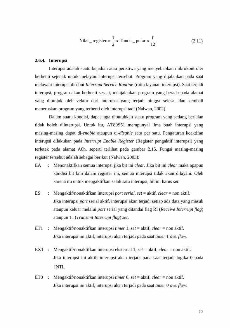
2.6.4. Interupsi
Interupsi adalah suatu kejadian atau peristiwa yang menyebabkan mikrokontroler
berhenti sejenak untuk melayani interupsi tersebut. Program yang dijalankan pada saat
melayani interupsi disebut Interrupt Service Routine (rutin layanan interupsi). Saat terjadi
interupsi, program akan berhenti sesaat, menjalankan program yang berada pada alamat
yang ditunjuk oleh vektor dari interupsi yang terjadi hingga selesai dan kembali
meneruskan program yang terhenti oleh interupsi tadi (Nalwan, 2002).
Dalam suatu kondisi, dapat juga dibutuhkan suatu program yang sedang berjalan
tidak boleh diinterupsi. Untuk itu, AT89S51 mempunyai lima buah interupsi yang
masing-masing dapat di-enable ataupun di-disable satu per satu. Pengaturan keaktifan
interupsi dilakukan pada Interrupt Enable Register (Register pengaktif interupsi) yang
terletak pada alamat A8h, seperti terlihat pada gambar 2.15. Fungsi masing-masing
register tersebut adalah sebagai berikut (Nalwan, 2003):
EA : Menonaktifkan semua interupsi jika bit ini clear. Jika bit ini clear maka apapun
kondisi bit lain dalam register ini, semua interupsi tidak akan dilayani. Oleh
karena itu untuk mengaktifkan salah satu interupsi, bit ini harus set.
ES : Mengaktif/nonaktifkan interupsi port serial, set = aktif, clear = non aktif.
Jika interupsi port serial aktif, interupsi akan terjadi setiap ada data yang masuk
ataupun keluar melalui port serial yang ditandai flag RI (Receive Interrupt flag)
ataupun TI (Transmit Interrupt flag) set.
ET1 : Mengaktif/nonaktifkan interupsi timer 1, set = aktif, clear = non aktif.
Jika interupsi ini aktif, interupsi akan terjadi pada saat timer 1 overflow.
EX1 : Mengaktif/nonaktifkan interupsi eksternal 1, set = aktif, clear = non aktif.
Jika interupsi ini aktif, interupsi akan terjadi pada saat terjadi logika 0 pada
1INT .
ET0 : Mengaktif/nonaktifkan interupsi timer 0, set = aktif, clear = non aktif.
Jika interupsi ini aktif, interupsi akan terjadi pada saat timer 0 overflow.
17

EX0 : Mengaktif/nonaktifkan interupsi eksternal 1, set = aktif, clear = non aktif.
Jika interupsi ini aktif, interupsi akan terjadi pada saat terjadi logika 0 pada
0INT .
Dapat diakses secara bit (bit addressable)
A8h EA ES ET1 EX1 ET0 EX0
IE.7 IE.4 IE.3 IE.2 IE.1 IE.0
Gambar 2.15. Register IE (Nalwan, 2003)
Gambar 2.16. Sumber interupsi (Atmel, 2001)
Interupsi eksternal 0INT dan 1INT dapat dipilih dengan dua macam pilihan
aktivasi, yaitu: aktivasi tingkat (level-activated) atau aktivasi transisi (transition-
activated), yang tergantung dari pengesetan bit IT0 dan IT1 dalam register TCON, seperti
terlihat pada gambar 2.14. Pada gambar 2.16 terlihat bahwa tanda atau flag yang
sesungguhnya menghasilkan interupsi ini adalah bit-bit IE0 (TCON.1) dan IE1 (TCON.3)
yang juga terdapat dalam register TCON. Saat rutin layanan interupsi eksternal
dijalankan, mikrokontroler akan secara otomatis me-nol-kan tanda interupsi terkait
seandainya interupsi tersebut diaktivasi dengan keaktifan transisi. Jika interupsi tersebut
diaktivasi secara level atau tingkat, maka sumber eksternal-lah yang mengontrol tanda
interupsi tersebut (Putra, 2002).
18

2.7. Rangkaian Single Chip Microcontroller
VCC
11,0592 MHz
10uF/16V
33pF
X1
EA/VP
RESET
VCCAT89S51
X28k2
33pF
Gambar 2.17. Rangkaian single chip microcontroller
Seperti terlihat pada gambar 2.17, rangkaian single chip microcontroller hanya
memerlukan sebuah osilator yang terdiri dari sebuah kristal dan dua buah kapasitor, serta
rangkaian reset yang terdiri atas sebuah resistor dan kapasitor. Pada rangkaian single chip,
kaki VPP/EA perlu dihubungkan ke Vcc untuk membuat akses awal mikrokontroler
berasal dari alamat 000H Flash PEROM. Apabila kaki VPP/EA terhubung ke ground
maka akses awal akan berasal dari alamat 000H memori eksternal (Nalwan, 2003).
Sementara itu, untuk membuat rangkaian reset secara manual cukup ditambahkan
sebuah resistor dan tombol push-button seperti terlihat pada gambar 2.18. Saat saklar
ditekan, aliran arus akan mengalir dari VCC melalui R1 menuju ke kaki RESET. Tegangan
di kaki RESET atau VR2 akan bernilai (Nalwan, 2003):
CCxV2R1R
2R2VR+
= (2.12)
Dengan memasukkan nilai-nilai resistor seperti tercantum pada gambar 2.18 pada
persamaan 2.6 maka tegangan VR2 saat saklar ditekan akan bernilai 4,94 volt dengan
VCC = 5 volt. Tegangan 4,94 volt pada kaki RST akan menyebabkan kaki ini berlogika 1
pada saat saklar tersebut ditekan. Saat saklar dilepas, aliran arus dari VCC memalui R1
akan terhenti dan tegangan pada kaki RST akan turun menuju ke nol sehingga logika pada
kaki ini berubah menjadi 0 dan proses reset selesai (Nalwan, 2003).
19

VCC
R1100
RESET
VCC
R28,2K
10uF/16V
Gambar 2.18. Rangkaian reset secara manual (Nalwan, 2003)
2.8. Remote Control
Salah satu cara untuk mengontrol peralatan secara remote namun masih berada
dalam area jarak padang adalah menggunakan cahaya infra merah. Infra merah
sebenarnya merupakan cahaya biasa dengan warna tertentu. Manusia tidak dapat melihat
warna dari sinar ini karena panjang gelombangnya berada dibawah spektrum cahaya
tampak. Meskipun manusia tidak dapat melihat cahaya infra merah yang diemisikan oleh
remote control namun tidak berarti cahaya tersebut tidak dapat dilihat. Kamera video atau
kamera foto digital dapat digunakan untuk menangkap sinar tersebut. (Bergmans, 2001)
Infra merah merupakan subjek yang sangat menarik dalam bidang pengontrolan
dan komunikasi. Hal ini dikarenakan ia mudah dihasilkan dan tidak mengalami
interferensi elektromagnetik. Namun sinar ini tidak begitu sempurna karena terdapat
begitu banyak benda yang dapat menghasilkan infra merah. Segala sesuatu yang dapat
menghasilkan panas dapat meradiasikannya, misalnya: matahari, lampu, oven, kompor,
mesin mobil, air panas, dan bahkan tubuh manusia dapat meradiasikan infra merah. Oleh
karena itu diperlukan suatu “kunci” supaya receiver dapat membedakan antara data
transmisi yang sesungguhnya dan noise-noise yang dihasilkan lingkungan di sekitarnya.
(Lipnharski, 2003)
Modulasi merupakan jawaban untuk mengatasi masalah tersebut. Dengan
modulasi, sumber sinar infra merah dibuat berkedap-kedip dengan frekuensi carrier
tertentu. Receiver-nya kemudian di-tuned dengan frekuensi yang sama sehingga ia akan
mengabaikan sinyal-sinyal yang lain. Frekuensi carrier yang dipakai biasanya antara 30 –
60 kHz. (Bergmans, 2001). Gelombang dengan frekuensi carrier ini kemudian digunakan
untuk merepresentasikan kode “1” dalam komunikasi digital. Sementara kode “0”
direpresentasikan dengan ketiadaan sinyal dari transmitter. Gambar 2.19 menunjukkan
pemodulasian sinyal infra merah.
20

Gambar 2.19. Pemodulasian sinyal infra merah (Bergmans, 2001)
2.8.1. SONY Remote Control
Untuk menghindari kemungkinan remote control dari suatu produsen elektronik
mengintervensi peralatan elektronik dari perusahaan lain maka setiap produsen elektronik
menggunakan protokol dan pengkodean yang berbeda satu dengan yang lain. Sehingga
meskipun mereka menggunakan frekuensi carrier yang sama, namun interferensi akan
dapat dihindari karena sistem pengkodeannya berbeda. (Lipnharski, 2003).
Sony menggunakan protokol SIRC (Serial Infra Red Control) yang menggunakan
teknik pengkodean lebar pulsa atau pulse-width codification. Pada pengkodean ini, pulsa
yang merepresentasikan logika “1” adalah rentetan gelombang carrier 40 kHz selama 1,2
milidetik, sementara lama rentetan untuk logika 0 adalah 0,6 milidetik. Semua bit
dipisahkan oleh interval diam selama 0,6 milidetik (Bergsman, 2003). Pengkodean lebar
pulsa SIRC Sony dapat dilihat pada gambar 2.20.
Gambar 2.20. Pengkodean lebar pulsa SIRC Sony (Bergsman, 2003)
Pada gambar 2.21 diperlihatkan urutan pulsa yang digunakan pada protokol SIRC.
Pada protokol ini LSB ditransmisikan terlebih dahulu. Start bit adalah rentetan
gelombang carrier selama 2,4 milidetik, diikuti interval diam selama 0,6 milidetik.
Kemudian dikirimkan 7-bit command, diikuti oleh 5-bit Device address. Seluruh rentetan
transmisi perintah akan diulang setiap 45 milidetik (diukur dari start ke start) selama
tombol yang sama pada remote control masih terus ditekan. (Bergsman, 2003)
21

Gambar 2.21. Protokol SIRC Sony (Bergsman, 2003)
2.6.2. IR Receiver Module
Pada gambar 2.22 diperlihatkan diagram blok dasar sebuah receiver infra merah.
Sinyal transmisi infra merah diterima oleh photodiode infra merah pada bagian kiri
diagram blok. Sinyal yang diterima kemudian dikuatkan dan dibatasi pada dua blok
selanjutnya. Limiter bertindak sebagai rangkaian AGC (Auto Gain Control) untuk
mendapatkan level pulsa yang konstan berapapun jarak receiver dari transmitter. Dengan
adanya kapasitor maka hanya sinyal AC saja yang diteruskan ke BPF (Band Pass Filter).
BPF di-tuned pada frekuensi carrier remote control dan hanya akan melewatkan sinyal
dengan frekuensi yang sesuai. (Bergmans, 2001)
Gambar 2.22. Digram blok receiver infra merah (Bergmans, 2001)
Ketiga blok terakhir berfungsi untuk mendeteksi adanya frekuensi carrier. Jika
terdeteksi, maka output comparator akan ditarik ke logika “0”, demikian sebaliknya.
(Bergmans, 2001). Dari sini terlihat bahwa keluaran receiver adalah inverse atau
kebalikan dari data yang ditransmisikan oleh remote control.
2.9. Motor DC
Motor DC merupakan mesin listrik berputar yang didesain untuk bekerja
menggunakan sumber daya dari tegangan searah. Tipe dasar dari motor jenis ini adalah
motor DC magnet permanen. Bagian stator dari motor DC magnet permanen terdiri atas
dua atau lebih kutub magnet. Bagian rotor-nya terdiri dari atas lilitan-lilitan yang
terhubung ke komutator mekanik. Polaritas kutub yang berlawanan antara lilitan berarus
22

dan magnet pada stator akan saling menarik dan menyebabkan rotor berputar sampai
sejajar dengan stator. Pada saat rotor mencapai kesejajaran, sikat pada motor akan
mengenai kontak pada komutator dan menginduksi lilitan berikutnya (Freescale
Semiconductor, 2004-2005).
Prinsip kerja motor DC dapat dilihat pada gambar 2.23. Ketika arus listrik yang
dialirkan melalui kawat penghantar berada di dalam suatu medan magnet maka kawat
akan mengalami gaya magnet. Apabila kawat pengahantar tersebut berbentuk suatu
kalang (loop) maka kedua sisi dari kalang yang berada pada sudut yang tepat terhadap
arah medan magnet akan mengalami gaya yang saling berlawanan. Pasangan gaya yang
saling berlawanan tersebut akan menciptakan efek berputar atau torsi untuk memutar
lilitan. Komutator akan membalik arah arus kalang setiap setengah putaran untuk menjaga
supaya arah putar motor tetap sama (Nave, ---).
Gambar 2.23. Prinsip kerja motor DC (Nave, ---)
Dua tipe lain dari motor DC adalah motor DC kumparan seri dan motor DC
kumparan paralel. Motor-motor ini juga menggunakan rotor yang sama yakni memakai
sikat dan komutator. Namun, stator-nya menggunakan lilitan bukan magnet permanen.
Prinsip kerjanya tidak berbeda dengan motor sebelumnya. Motor DC kumparan seri
memiliki lilitan stator yang terhubung secara seri dengan rotor sedangkan motor DC
kumparan paralel mempunyai lilitan stator yang terhubung secara paralel dengan lilitan
rotor. Motor DC kumparan seri biasa juga disebut motor universal dalam artian motor ini
23
mampu beroperasi sama baiknya menggunakan sumber tegangan DC ataupun AC
(Freescale Semiconductor, 2004-2005).
2.10. Penampil Seven-Segment
Penampil seven-segment merupakan suatu perangkat elektronik yang terdiri dari 7
buah LED yang tersusun sesuai pola-pola numeris atau alfa-numeris. Dengan
mengaktifkan LED-LED tertentu akan dapat dihasilkan tampilan angka atau huruf sesuai
yang dikehendaki. Sebagai kelengkapan, biasanya seven-segment juga dilengkapi dengan
satu atau dua LED tambahan untuk menampilkan titik pecahan. (Answers.com, 2005).
Bentuk fisik dan penempatan dioda dalam seven-segment dapat dilihat pada gambar 2.24.
(a)
(b)
Gambar 2.24. Seven-segment (a) Bentuk fisik (Answers.com, 2005) (b) Penempatan dioda (hibp.ecse.rpi.edu)
D C
G
B
E
E
VCC
AB
A
F
F
C
D G D
GCE
B
A
E
FB
AA
D
F
C
(a) (b) Gambar 2.25. Pengkabelan internal seven-segment (hibp.ecse.rpi.edu)
(a) Common anoda (b) Common katoda
24
Terdapat dua tipe seven-segment berdasarkan commonnya, yaitu: common anoda
dan common katoda (hibp.ecse.rpi.edu). Common anoda berarti kaki anoda dari masing-
masing LED dihubungkan menjadi satu dengan Vcc sementara kaki-kaki katoda
digunakan sebagai selektor LED yang akan diaktifkan. Kondisi keaktifan kaki katoda
pada common ini adalah aktif rendah. Sementara pada common katoda, kaki-kaki anoda
digunakan sebagai selektor sedangkan kaki katoda setiap LED dihubungkan ke ground.
Kondisi keaktifan kaki anoda pada common katoda ini adalah aktif tinggi. Diagram
pengkabelan common anoda dan common katoda seven-segment dapat dilihat pada
gambar 2.25.
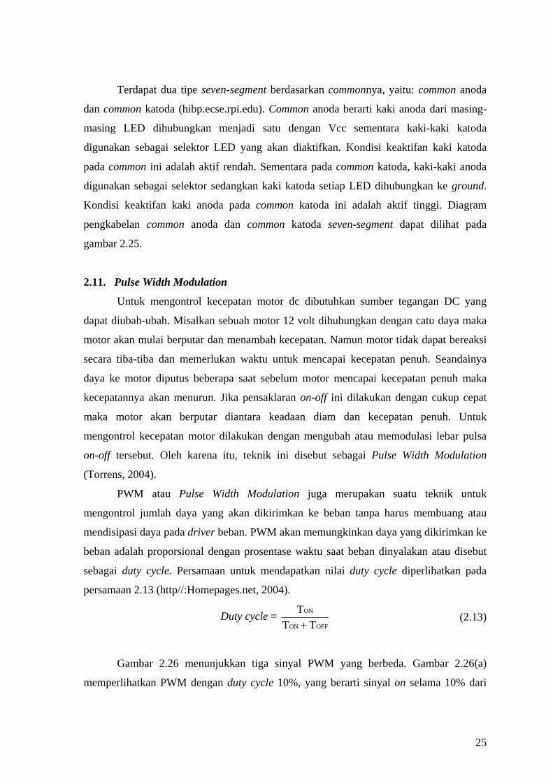
2.11. Pulse Width Modulation
Untuk mengontrol kecepatan motor dc dibutuhkan sumber tegangan DC yang
dapat diubah-ubah. Misalkan sebuah motor 12 volt dihubungkan dengan catu daya maka
motor akan mulai berputar dan menambah kecepatan. Namun motor tidak dapat bereaksi
secara tiba-tiba dan memerlukan waktu untuk mencapai kecepatan penuh. Seandainya
daya ke motor diputus beberapa saat sebelum motor mencapai kecepatan penuh maka
kecepatannya akan menurun. Jika pensaklaran on-off ini dilakukan dengan cukup cepat
maka motor akan berputar diantara keadaan diam dan kecepatan penuh. Untuk
mengontrol kecepatan motor dilakukan dengan mengubah atau memodulasi lebar pulsa
on-off tersebut. Oleh karena itu, teknik ini disebut sebagai Pulse Width Modulation
(Torrens, 2004).
PWM atau Pulse Width Modulation juga merupakan suatu teknik untuk
mengontrol jumlah daya yang akan dikirimkan ke beban tanpa harus membuang atau
mendisipasi daya pada driver beban. PWM akan memungkinkan daya yang dikirimkan ke
beban adalah proporsional dengan prosentase waktu saat beban dinyalakan atau disebut
sebagai duty cycle. Persamaan untuk mendapatkan nilai duty cycle diperlihatkan pada
persamaan 2.13 (http//:Homepages.net, 2004).
Duty cycle = OFFON
ON
TTT+
(2.13)
Gambar 2.26 menunjukkan tiga sinyal PWM yang berbeda. Gambar 2.26(a)
memperlihatkan PWM dengan duty cycle 10%, yang berarti sinyal on selama 10% dari
25

total periode dan off selama 90% sisanya. Sementara gambar 2.26(b) dan 2.26(c)
memperlihatkan PWM dengan duty cycle 50% dan 90% (Barr, 2001).
Gambar 2.26. Sinyal PWM dengan duty cycle bervariasi (Barr, 2001)
2.12. Transistor sebagai saklar
Pada saat digunakan sebagai saklar, transistor biasanya dioperasikan pada kondisi
cutoff dan saturasi. Gambar 2.27 mengilustrasikan prinsip kerja transistor sebagai
peralatan pensaklaran. Pada gambar 2.27(a) transistor berada pada daerah cutoff karena
junction basis-emitornya tidak dibias maju. Pada kondisi ini, secara ideal antara kolektor
dan emitor terjadi open circuit seperti diilustrasikan oleh gambar saklar yang terbuka
(Floyd, 1996).
Gambar 2.27. Transistor NPN sebagai saklar pada kondisi ideal versi electron flow
(Floyd, 1996)
Pada gambar 2.27(b), transistor berada pada daerah saturasi karena junction basis-
emitor dan junction basis-kolektor dibias maju, serta arus basis dibuat cukup besar yang
26

menyebabkan arus kolektor mencapai nilai saturasinya. Pada kondisi ini, secara ideal,
terjadi short antara kolektor dan emitor seperti diilustrasikan oleh saklar yang tertutup.
Sebenarnya, pada kolektor-emitor terjadi penurunan tegangan pada kisaran kurang dari 1
volt, yang disebut tegangan saturasi atau VCE(sat) (Floyd, 1996).
2.10.1. Kondisi Cutoff
Transistor berada pada kondisi cutoff ketika junction basis-emitor tidak dibias
maju. Dengan mengabaikan arus bocor, maka semua arus adalah nol, dan VCE sama
dengan VCC (Floyd, 1996). Hal ini diperlihatkan oleh persamaan 2.14.
VCE(cutoff) = VCC (2.14)
2.10.2. Kondisi saturasi
Transistor berada pada kondisi saturasi ketika junction basis-emitor dibias maju
dan terdapat arus basis yang cukup besar untuk memproduksi arus kolektor secara
maksimum (Floyd, 1996). Persamaan untuk mendapatkan arus kolektor saturasi
diperlihatkan pada persamaan berikut:
IC(sat) = C
)sat(CECC
RVV −
Seandainya IC(sat) diketahui maka untuk mencari nilai RC dapat dicari dengan
menggunakan persamaan 2.15.
)sat(C
)sat(CECCC I
VVR
−= (2.15)
Untuk menjamin bahwa transistor benar-benar berada pada kondisi saturasi maka
IB harus jauh lebih besar dibandingkan IB(min) (Floyd, 1996). Persamaan untuk
mendapatkan IB(min) diperlihatkan pada persamaan 2.16.
DC
)sat(C(min)B
IIβ
= (2.16)
Sedangkan untuk menentukan nilai RB dapat dicari dengan menggunakan
persamaan 2.17.
B
RBB I
VR = (2.17)
27

Rangkaian transistor PNP sebagai saklar memiliki persamaan yang sama dengan
transistor NPN. Perbedaan antara keduanya adalah pada arah arus yang mengalir yang
saling berkebalikan. Rangkaian saklar menggunakan transistor PNP diperlihatkan pada
gambar 2.28.
(a) (b) Gambar 2.28 Transistor PNP sebagai saklar pada kondisi ideal versi electron flow
(a) Saturasi – saklar tertutup (b) Cutoff – saklar terbuka
2.13. H-bridge
H-bridge atau biasa disebut full bridge, diberi nama demikian karena memiliki
empat buah saklar pada ujung kaki-kaki H, dan sebuah motor membentuk garis horisontal
sehingga menyerupai huruf H. Keempat saklar tesebut, apabila diurutkan menurut arah
berlawanan jarum jam, adalah high side left, high side right, low side right, dan low side
right. Supaya bekerja dengan benar, saklar-saklar tersebut harus dinyalakan secara
berpasangan, yaitu pasangan high-left dan low-right, atau low-left dan high-right.
Menyalakan kedua saklar pada kedua sisi kiri atau kanan yang sama adalah terlarang,
karena akan menyebabkan short circuit. (McManis, 2003). Rangkaian dasar sebuah H-
bridge diperlihatkan pada gambar 2.29.
Gambar 2.29. Rangkaian dasar sebuah H-bidge (McManis, 2003)
28

IC L293D merupakan quadruple high current half-H drivers. L293D didesain
untuk menghasilkan arus bidireksional sampai 600 mA pada rentang tegangan 4,5 V
sampai 36 V. IC ini didesain untuk men-drive beban induktif seperti relay, solenoida,
motor DC dan stepper, serta beban-beban lainnya. Driver motor ini diaktifkan secara
berpasangan, dengan driver 1 dan 2 di-enable oleh pin 1,2 EN dan driver 3 dan 4 di-
enable oleh pin 3,4EN. Saat kondisi input enable adalah high, output mereka akan aktif
dan mengeluarkan pulsa dengan fase yang sama dengan input-nya. Apabila kondisi input
enable adalah low, output yang bersangkutan akan off dan berada pada kondisi high-
impedance (Texas Instrument, 2002).
(a) (b)
Gambar 2.30 Diagram internal IC L293D (Texas Instrument, 2002) (a) Simbol hubungan I/O (b) Rangkaian I/O internal
Dengan memberikan data input yang benar, setiap pasangan driver akan
membentuk jembatan H penuh atau full-H yang dapat digunakan untuk mengendalikan
arah putar motor secara bolak-balik. Selain itu, pada IC ini juga disediakan dua buah
power supply yang terpisah, masing-masing untuk power supply data TTL dan power
supply beban untuk meminimalkan disipasi daya. Sebagai pengaman, sebaiknya
29

ditambahkan diode berkecepatan tinggi untuk meredam arus transient induktif. Tabel
kebenaran IC L293D dapat dilihat pada tabel 2.3, sementara diagram internalnya
ditunjukkan pada gambar 2.30 (Texas Instruments, 2002).
Tabel 2.3 Tabel kebenaran IC L293D untuk tiap driver (Texas Instrument, 2002)
Input
A EN
Output
Y
H H H
L H L
X L Z
Ket: H = High, L = Low, Z = High Impedance (off)
30

BAB III
PERANCANGAN
Laser show pada dasarnya merupakan suatu hiburan yang dihasilkan dari
manipulasi sinar laser untuk mendapatkan pola-pola geometris tertentu. Secara
sederhana, hal ini dapat dilakukan dengan memantulkan sinar laser terhadap satu atau
beberapa cermin yang berputar sebelum akhirnya dipantulkan ke dinding atau layar.
Tampilan pada layar inilah yang kemudian dapat diamati sebagai pola-pola geometris.
Untuk menghasilkan berbagai variasi pola, terdapat tiga unsur yang harus
diperhatikan, yang pertama adalah putaran cermin harus sedikit bergoyang. Tujuannya
supaya terbentuk perbedaan sudut ketika sinar memantul. Hal ini dapat dicapai
dengan menempelkan cermin ke motor dengan sudut kemiringan tertentu.
Unsur lainnya adalah putaran motor yang stabil namun tetap memberikan
kemudahan dalam pengaturan kecepatan maupun arah putar. Variasi arah putar dan
kecepatan ini akan menentukan banyak sedikitnya pola yang dapat dihasilkan.
Semakin luas range kecepatan motor maka semakin banyak pula pola yang dapat
terbentuk. Begitu pula apabila motor dapat berputar dua arah, CW dan CCW, maka
polanya juga semakin banyak. Pengaturan kecepatan dan arah ini akan semakin
mudah dan akurat apabila diatur secara digital dibanding secara analog.
Unsur terakhir adalah jumlah cermin. Semakin banyak media pemantulan
maka kombinasi pola yang terbentuk juga semakin besar. Namun harus tetap
diperhatikan bahwa semakin banyak jumlah cermin maka kemungkinan sinar tidak
mengenai cermin ke-n juga semakin besar. Hal ini dikarenakan putaran cemin yang
bergoyang akan menyebabkan pantulan sinar membentuk sudut dan akibatnya adalah
luas daerah jatuh sinar menjadi semakin luas. Semakin banyak jumlah pantulan maka
luas daerah tersebut juga semakin luas. Oleh karena itu perlu dicari jumlah cermin
serta jarak antar cermin yang paling optimal.
3.1. Diagram Kotak Digital Laser Show
Secara garis besar, perancangan digital laser show terdiri atas perancangan
perangkat keras dan perangkat lunak. Perangkat keras secara umum dapat dibagi
menjadi tiga bagian, yaitu unit masukan, unit pengendali kecepatan motor, dan unit
31
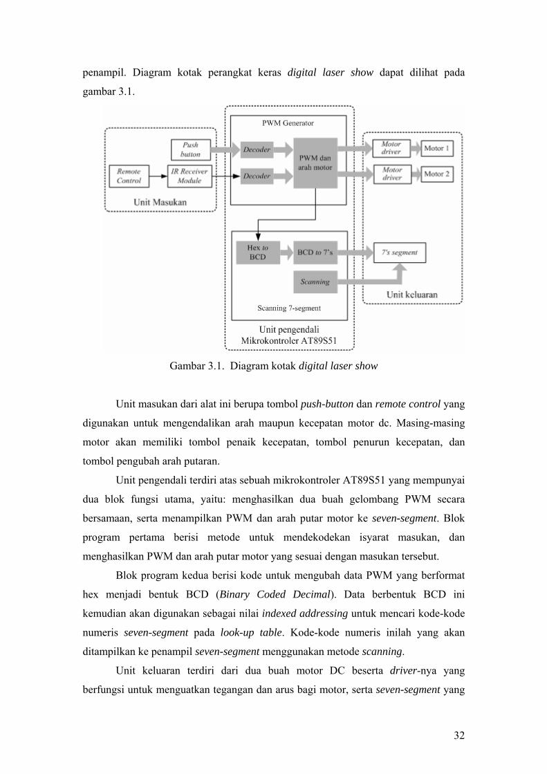
penampil. Diagram kotak perangkat keras digital laser show dapat dilihat pada
gambar 3.1.
Gambar 3.1. Diagram kotak digital laser show
Unit masukan dari alat ini berupa tombol push-button dan remote control yang
digunakan untuk mengendalikan arah maupun kecepatan motor dc. Masing-masing
motor akan memiliki tombol penaik kecepatan, tombol penurun kecepatan, dan
tombol pengubah arah putaran.
Unit pengendali terdiri atas sebuah mikrokontroler AT89S51 yang mempunyai
dua blok fungsi utama, yaitu: menghasilkan dua buah gelombang PWM secara
bersamaan, serta menampilkan PWM dan arah putar motor ke seven-segment. Blok
program pertama berisi metode untuk mendekodekan isyarat masukan, dan
menghasilkan PWM dan arah putar motor yang sesuai dengan masukan tersebut.
Blok program kedua berisi kode untuk mengubah data PWM yang berformat
hex menjadi bentuk BCD (Binary Coded Decimal). Data berbentuk BCD ini
kemudian akan digunakan sebagai nilai indexed addressing untuk mencari kode-kode
numeris seven-segment pada look-up table. Kode-kode numeris inilah yang akan
ditampilkan ke penampil seven-segment menggunakan metode scanning.
Unit keluaran terdiri dari dua buah motor DC beserta driver-nya yang
berfungsi untuk menguatkan tegangan dan arus bagi motor, serta seven-segment yang
32

berfungsi untuk menampilkan data persentase duty cycle dan arah putar masing-
masing motor.
3.2. Konstruksi Digital Laser Show
Sebagai sarana pengaman, rangkaian elektronis perangkat digital laser show
akan dimasukkan ke dalam suatu kotak yang solid dan kokoh yang terbuat dari bahan
isolator untuk mengurangi kemungkinan terjadinya kerusakan komponen serta
melindungi user dari kemungkinan tersengat arus listrik. Laser yang akan digunakan
merupakan laser pointer yang merupakan laser jenis He-Ne (Helium-Neon) berwarna
merah dengan panjang gelombang 0,663 mikron.
Piranti masukan berupa tombol-tombol push-button akan diletakkan di bagian
atas kotak untuk memudahkan pengontrolan, sementara piranti masukan lainnya yaitu
IR receiver module akan diletakkan di bagian dalam sisi depan kotak untuk
menangkap sinyal remote secara maksimal. Piranti penampil berupa seven-segment
juga akan diletakkan pada bagian dalam sisi depan kotak untuk memudahkan dalam
pengamatan data. Konstruksi digital laser show secara lengkap dapat dilihat pada
gambar 3.2. Fitur-fitur yang tersedia pada perangkat ini antara lain:
1. Pengontrolan kecepatan dan arah putar motor secara digital. Pengontrolan secara
digital akan memungkinkan pengontrolan yang lebih mudah dan sederhana, serta
lebih presisi dibandingkan pengontrolan secara analog.
2. Pengontrolan kecepatan dan arah putar motor dapat dilakukan secara nirkabel
menggunakan remote control ataupun secara konvensional menggunakan tombol
push-button. Pengontrolan secara nirkabel akan memungkinkan user mengontrol
dari kejauhan dan menikmati suguhan pola-pola pantulan yang dihasilkan dengan
lebih santai dan nyaman. Selain itu pengontrolan jarak jauh juga relatif lebih aman
karena akan mengurangi kemungkinan jatuhnya sinar laser ke mata yang
berpotensi mengurangi kemampuan penglihatan. Pengontrolan secara nirkabel ini
dapat dilakukan dengan menggunakan remote control untuk TV Sony Triniton
yang banyak tersedia di pasaran.
3. Derajat kenaikan atau penurunan duty cycle PWM sebagai pengatur kecepatan
motor adalah sebesar 1% yang akan memberikan tingkat kepresisian yang cukup
tinggi, serta range kecepatan yang luas. Range kecepatan yang luas ini akan
memungkinkan jumlah variasi rasio kecepatan antara motor pertama dan kedua
33

yang semakin banyak. Hal ini pada akhirnya akan menyebabkan pola pantulan
laser yang semakin banyak dan variatif.
Gambar 3.2 Layout digital laser show
Keterangan gambar:
1. Layar 6. Tombol push-button
2. Pantulan sinar laser 7. IR Receiver module
3. Laser pointer 8. Penampil seven-segment
4. Motor DC 9. Kode fungsi tombol
5. Cermin 10. Pola yang dihasilkan
4. Kemampuan untuk mengatur arah putar motor. Kemampuan motor untuk berputar
dua arah, yaitu searah (CW) dan berlawanan (CCW) arah jarum jam juga akan
menyebabkan pola pantulan laser yang semakin banyak dan variatif.
5. Sarana penampil yang cukup terang dan jelas meskipun dilihat dari kejauhan
karena menggunakan display seven-segment, bukan LCD.
6. Desain keseluruhan yang kompak dan portable sehingga memudahkan untuk
digunakan, dipindahkan, dan disimpan.
34
3.3. Input Interface
Untuk memberikan keleluasaan dan kenyamanan dalam mengoperasikan
perangkat digital laser show ini maka disediakan dua teknik pemberian masukan yang
dapat digunakan sesuai keinginan user. Kedua teknik tersebut adalah pengontrolan
menggunakan tombol push-button yang terpasang secara on-board, serta pengontrolan
secara nirkabel atau remote menggunakan remote control.
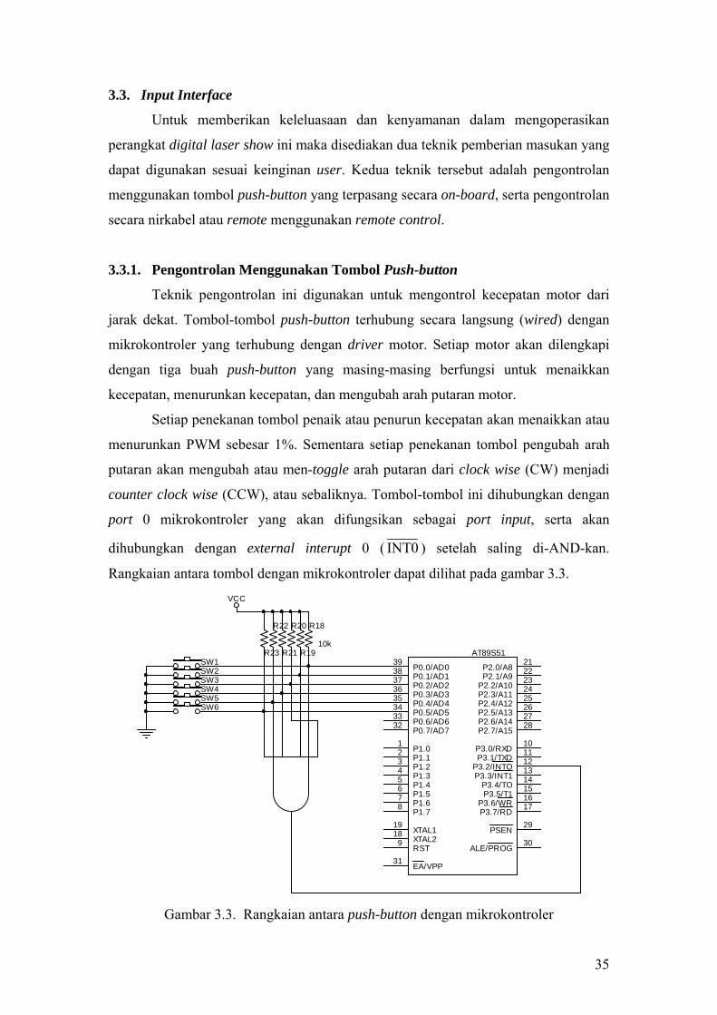
3.3.1. Pengontrolan Menggunakan Tombol Push-button
Teknik pengontrolan ini digunakan untuk mengontrol kecepatan motor dari
jarak dekat. Tombol-tombol push-button terhubung secara langsung (wired) dengan
mikrokontroler yang terhubung dengan driver motor. Setiap motor akan dilengkapi
dengan tiga buah push-button yang masing-masing berfungsi untuk menaikkan
kecepatan, menurunkan kecepatan, dan mengubah arah putaran motor.
Setiap penekanan tombol penaik atau penurun kecepatan akan menaikkan atau
menurunkan PWM sebesar 1%. Sementara setiap penekanan tombol pengubah arah
putaran akan mengubah atau men-toggle arah putaran dari clock wise (CW) menjadi
counter clock wise (CCW), atau sebaliknya. Tombol-tombol ini dihubungkan dengan
port 0 mikrokontroler yang akan difungsikan sebagai port input, serta akan
dihubungkan dengan external interupt 0 ( 0INT ) setelah saling di-AND-kan.
Rangkaian antara tombol dengan mikrokontroler dapat dilihat pada gambar 3.3.
R23
R20 R18
10k
SW1
SW3
AT89S51
91819 29
30
31
12345678
2122232425262728
1011121314151617
3938373635343332
RSTXTAL2XTAL1 PSEN
ALE/PROG
EA/VPP
P1.0P1.1P1.2P1.3P1.4P1.5P1.6P1.7
P2.0/A8P2.1/A9
P2.2/A10P2.3/A11P2.4/A12P2.5/A13P2.6/A14P2.7/A15
P3.0/RXDP3.1/TXD
P3.2/INTOP3.3/INT1
P3.4/TOP3.5/T1
P3.6/WRP3.7/RD
P0.0/AD0P0.1/AD1P0.2/AD2P0.3/AD3P0.4/AD4P0.5/AD5P0.6/AD6P0.7/AD7
SW2
R19
R22
VCC
SW4SW5
R21
SW6
Gambar 3.3. Rangkaian antara push-button dengan mikrokontroler
35

Masing-masing tombol juga akan diberi R pull-up yang terhubung ke Vcc
sehingga logika port pada saat kondisi tombol idle (tidak ditekan) adalah “1”. Pada
saat tombol ditekan maka arus akan mengalir ke ground sehingga pin yang terhubung
dengan tombol yang ditekan akan berlogika “0”. Hal ini juga akan mengakibatkan
0INT bernilai “0” karena salah satu kaki gerbang AND bernilai “0”. 0INT
diprogram untuk terpicu karena adanya transisi negatif (negative-edge).
Setelah terdeteksi adanya interupsi penekanan tombol pada 0INT , kemudian
akan dilakukan pembacaan tombol. Metode pembacaan tombol yang digunakan
adalah dengan metode pembandingan antara logika-logika pada port dengan nilai
yang ditentukan oleh program. Metode pembacaan ini akan dijelaskan lebih lanjut
pada bagian perancangan perangkat lunak.
3.3.2. Pengontrolan Secara Nirkabel Menggunakan Remote Control
Pengontrolan ini digunakan untuk mengendalikan peralatan dari jarak jauh
secara remote atau nirkabel. Pengontrolan dilakukan dengan menekan tombol-tombol
yang terdapat pada remote control yang kemudian akan ditransmisikan menggunakan
sinar infra merah termodulasi. Sinyal ini kemudian akan diterima oleh IR receiver
module yang terhubung dengan mikrokontroler. Remote control yang digunakan
adalah remote control untuk SONY TRINITON dengan tipe RM-687C. Sementara
receiver yang digunakan adalah receiver infra merah standar yang terdapat di pasaran.
Kaki output dari receiver akan dihubungkan dengan kaki INT1 dari
mikrokontroler yang diprogram untuk terpicu saat mendeteksi transisi negatif
(negative edge). Karena kondisi keluaran receiver adalah berkebalikan (inverse) dari
remote control maka kondisi idle keluaran receiver adalah “1”. Pada saat terjadi
transisi dari kondisi “1” ke “0” maka INT1akan aktif dan mikrokontroler akan
melakukan pembacaan sinyal yang dikirimkan. Metode pembacaan sinyal ini akan
dibahas lebih lanjut pada bagian perancangan perangkat lunak.
Rangkaian antara receiver dengan mikrokontroler dapat dilihat pada gambar
3.4. Kapasitor dan resistor yang terhubung dengan kaki Vcc digunakan untuk men-
decouple interferensi yang mungkin ditimbulkan oleh komponen-komponen lain
dalam rangkaian. Sementara LED digunakan sebagai indikator apabila terdapat
transmisi sinyal dari remote control. Casing dari modul receiver juga perlu
36

dihubungkan dengan ground untuk menghindari interferensi dari sumber-sumber infra
merah lainnya. Hal ini dikarenakan modul IR receiver sangat peka terhadap
gangguan.
22 uF
P3.3/INT1
330
330IR RECEIVER
Vout
D1
LED
VCC
VCCAT89S51
VCC
Gambar 3.4. Rangkaian antara IR receiver dengan mikrokontroler
3.4. Driver Motor DC
Pada perancangan peralatan digital laser show ini, driver motor yang
digunakan adalah IC L293D. Setiap keping IC L293D mempunyai dua buah channel
input dan output yang saling terpisah sehingga dapat digunakan untuk mengendalikan
dua buah motor DC secara independen. L293D juga menyediakan dua catu daya yang
terpisah, yaitu untuk catu daya logika TTL dan catu daya motor, sehingga motor dapat
bekerja secara optimal sesuai dengan tegangan dan arus yang dibutuhkannya
walaupun dikendalikan dengan level logika TTL. VSS
VSS
P1.0M2 MOTOR DC
12
VSS
VCC
P2.3
U1
L293D
27
1015
19
361114
16
8
1A2A3A4A
1,2EN3,4EN
1Y2Y3Y4Y
VC
C
VSS
P2.2P2.1P2.0
AT89S51 VSS
VSS
M1 MOTOR DC
12
P1.1
Gambar 3.5. Rangkaian driver motor DC
37

Rangkaian driver motor dapat dilihat pada gambar 3.5. Keempat buah dioda
yang terhubung pada setiap motor digunakan untuk melindungi driver motor dari
tegangan balik yang dihasilkan kumparan motor saat disaklar on dan off. Input 1A dan
2A L293D yang dihubungkan dengan pin P2.0 dan P2.1 mikrokontroler, secara
berpasangan berfungsi untuk menentukan arah putaran motor DC pertama. Arah
putaran motor yang dihasilkan dari kombinasi logika input 1A dan 2A dapat dilihat
pada tabel 3.1.
Tabel 3.1. Arah putaran motor DC 1A 2A Putaran motor DC
0 0 Free running
0 1 CCW
1 0 CW
1 1 Brake
Input 1,2EN yang dihubungkan dengan pin P1.0 mikrokontroler berfungsi
untuk mengaktifkan atau menonaktifkan driver L293D. Pada saat kondisi input 1,2
EN high, rangkaian output internal IC L293D akan aktif. Seandainya pada saat yang
bersamaan, input 1A berlogika ”1” dan input 2A berlogika ”0” maka akan terdapat
arus mengalir dari output 1Y ke 2Y melalui motor yang akan menyebabkan motor
berputar CW. Seandainya pada saat tersebut, input 1A berlogika ”0” dan input 2A
berlogika ”1” maka arah putar akan berlawanan karena arus mengalir dari output 2Y
ke 1Y.
Dari penjelasan diatas dapat ditarik benang simpul bahwa input 1,2EN
mengendalikan kondisi keaktifan driver L293D. Logika “1” pada input ini akan
menyebabkan motor DC pertama berputar, dan logika “0” tidak berputar. Apabila
sinyal pada kaki 1,2 EN diberi rentetan logika “1” dan “0” dengan sangat cepat
menggunakan sinyal PWM maka kecepatan motor DC akan dapat dikendalikan.
Metode untuk menghasilkan sinyal PWM akan dijelaskan lebih lanjut pada bagian
perancangan perangkat lunak. Input 3A dan 4A, serta 3,4 EN digunakan untuk
mengendalikan motor DC kedua dengan fungsi seperti input 1A, 2A, dan 1,2EN.
Motor yang akan digunakan adalah motor DC yang digunakan pada pemutar
CD (CD ROM) dengan tegangan 12V. Alasan penggunaan motor ini adalah karena
respon tegangannya yang sangat baik. Motor sudah mampu berputar walaupun
tegangan input yang diberikan masih sangat rendah sehingga diharapkan pada saat
38

diaplikasikan menggunakan PWM, motor dapat bekerja dalam range kecepatan yang
luas.
3.5. Penampil Seven-segment
Penampil seven-segment digunakan untuk menampilkan data PWM tiap motor
dan arah putaran motor. Setiap motor akan dilengkapi dengan tiga buah seven-
segment. Dua seven-segment menunjukkan data PWM dalam skala persen mulai dari
00 sampai dengan 99 persen. Sementara sisanya akan menampilkan arah putaran
motor. Pada perancangan ini digunakan seven-segment dengan tipe common anode.
AT89S512122232425262728
3938373635343332
P2.0/A8P2.1/A9
P2.2/A10P2.3/A11P2.4/A12P2.5/A13P2.6/A14P2.7/A15
P0.0/AD0P0.1/AD1P0.2/AD2P0.3/AD3P0.4/AD4P0.5/AD5P0.6/AD6P0.7/AD7
7's segment
42
91
67
10
3
BC516
VCC
3
2
1
VCC
RC
3
2
1
3
2
1
7's segment
42
91
67
10
3
BC516
R13
BC516
7's segment
42
91
67
10
3 3
2
1
BC516
VCCVCC
R14
R16
BC516
7's segment
42
91
67
10
3
BC516
VCC
RB
R17
2K2
VCC
3
2
1
180
R12
R15
7's segment
42
91
67
10
3 3
2
1
7's segment
42
91
67
103
Gambar 3.6. Rangkaian seven-segment
Seperti terlihat pada gambar 3.6, dalam perancangan terdapat lebih dari empat
buah seven-segment (sesuai jumlah port paralel mikrokontroler), oleh karena itu
digunakan metode scanning untuk mengaktifkan seluruh seven-segment. Metode
scanning merupakan metode untuk menyalakan seven-segment secara bergantian
dengan waktu yang sangat cepat. Penyala-padaman yang sangat cepat ini akan
menyebabkan ilusi pandangan pada mata sehingga akan terlihat seluruh seven-
segment menyala pada saat bersamaan. Hal ini dikarenakan mata tidak mampu
mengikuti frekuensi nyala-padam yang sangat cepat. Metode scanning ini akan
dijelaskan lebih lanjut pada bagian perancangan perangkat lunak.
39

Transistor yang akan digunakan sebagai saklar adalah transistor PNP
darlington seri BC516 yang mampu menyuplai arus kolektor IC hingga 1000 mA.
Nilai resistor RC dapat dihitung sesuai persamaan 2.15 dengan menambahkan
tegangan komponen LED.
LED
LED)sat(ECEEC I
VVVR
−−=
Dengan menggunakan nilai VEE = 5 V, VLED = 2,4 V, dan VCE(sat) = 1 V dari
datasheet, serta menentukan ILED = 10 mA maka dapat dicari nilai RC:
310.104,215
−
−−=CR
RC = 160 Ω, karena nilai ini tidak terdapat di pasaran maka dibulatkan menjadi:
RC = 180 Ω
Sementara untuk menentukan nilai RB dilakukan dengan mencari nilai IBmin
terlebih dahulu menggunakan persamaan 2.16.
DC
)sat(C(min)B
IIβ
=
Dengan menggunakan nilai βDC = 30.000 dari datasheet, dan arus LED seven-segment
sebesar 10 mA sebagai IC(sat) maka dapat dihitung nilai IB(min):
3
3
(min) 10.3010.10 −
=BI
IB(min) = 0,33 μA.
Untuk memastikan bahwa transistor benar-benar berada dalam kondisi saturasi maka
ditetapkan nilai IB yang akan digunakan adalah 2 mA. Dengan mengetahui nilai IB dan
VBE(sat) = 1,4 V dari datasheet maka nilai RB dapat dihitung menggunakan persamaan
2.17.
B
RBB I
VR = ,
dengan VRB = VEE – VBE(sat) maka:
310.24,15−
−=BR
RB = 1800 Ω, dan dibulatkan menjadi
RB = 2200 Ω
40

3.6. Perancangan Perangkat Lunak
3.6.1. Diagram Alir Utama
Gambar 3.7. Diagram alir utama
Seperti diperlihatkan pada gambar 3.7, diagram alir utama diawali dengan
proses inisialisasi kemudian diikuti dengan pengesetan kondisi awal PWM motor
serta pengesetan kondisi awal arah putar. Selanjutnya program akan melakukan
looping terus-menerus menunggu adanya sinyal interupsi.
Pada rantai program utama terlihat bahwa tidak ada instruksi yang dikerjakan
pada saat looping, hal ini dimaksudkan untuk mendapatkan tingkat efisiensi yang
tinggi sehingga program utama bisa dikembangkan untuk melakukan tugas-tugas
lainnya. Penulis mencoba untuk memaksimalkan fasilitas interupsi yang diberikan
oleh mikrokontroler sehingga program digital laser show ini dapat digunakan sebagai
add-on (tambahan) saja seandainya diinginkan pengembangan lebih lanjut dengan
mengisi looping program utama. Interupsi-interupsi yang digunakan untuk
menjalankan program dapat dilihat pada tabel 3.2.
Tabel 3.2. Interupsi yang digunakan pada program Digital Laser Show Jenis interupsi Interupt handler Fungsi
Interupsi penekanan
tombol
Interupsi eksternal 0 Interupsi untuk mendeteksi tombol masukan
Interupsi remote
control
Interupsi eksternal 1 Interupsi untuk mendekodekan sinyal remote control
Interupsi scanning
7-segment
Interupsi timer 0 Interupsi untuk melakukan scanning untuk
menampilkan data ke 7-segment
Interupsi PWM Interupsi timer 1 Interupsi untuk menghasilkan sinyal PWM tiap 1% duty
cycle
41

3.6.2. Diagram Alir Proses Inisialisasi Utama
Seperti terlihat pada gambar 3.9, diagram alir inisialisasi mikrokontroler
diawali dengan pendeklarasian konstanta-konstanta dan variabel-variabel pada RAM
internal, serta pendefinisian vektor-vektor interupsi. Kemudian dilakukan pengesetan
bagi timer, pengesetan aktivasi transisi negatif bagi interupsi eksternal, serta
pengaktifan semua interupsi eksternal dan timer.
Gambar 3.8. Diagram alir inisialisasi mikrokontroler
3.6.3 Interupsi Generator PWM
Pada penelitian ini kedua motor dirancang untuk dapat berputar dengan PWM
yang berbeda pada saat bersamaan. Program akan dimulai dengan mengurangi
counter sebesar satu poin dari nilai sebelumnya. Apabila counter telah bernilai nol,
maka counter akan di set ke nilai 100 yang merupakan nilai maksimal PWM dan
sinyal PWM akan dimatikan. Apabila belum, maka nilainya akan dibandingkan
dengan nilai PWM1 dan PWM2 yang ditentukan oleh user. Apabila nilainya sama,
maka sinyal sinyal PWM akan dinyalakan. Apabila tidak, maka sinyal PWM akan
mengikuti kondisi sebelumnya. Diagram alir interupsi timer sebagai pembangkit pulsa
PWM diperlihatkan pada gambar 3.9.
42

Gambar 3.9 Diagram alir interupsi timer 1: PWM
3.6.4. Interupsi penekanan tombol
Interupsi penekanan tombol terdeteksi dengan berubahnya kondisi bit 0INT
yang telah di-set untuk aktif karena terpicu transisi negatif (negative edge). Seperti
terlihat pada gambar 3.10, langkah pertama program adalah menonaktifkan semua
interupsi eksternal diikuti penyimpanan SFR ke stack pointer. Kemudian program
akan mendeteksi tombol mana yang ditekan dengan mendeteksi lokasi pin mana pada
port 0 yang berubah menjadi ”0”. Selanjutnya dilakukan penundaan untuk mengatasi
efek bouncing selama 20 mS.
Setelah itu dilakukan pengecekan kembali apakah tombol yang sama masih
ditekan? Apabila tidak maka program akan keluar dari proses interupsi. Apabila ya,
maka program akan menunggu sampai tombol dilepas sebelum menjalankan subrutin
yang sesuai dengan tombol yang ditekan. Sebagai langkah akhir program akan
mengambil kembali SFR dari stack pointer serta mengaktifkan kembali interupsi
eksternal.
43

Gambar 3.10 Diagram alir interupsi penekanan tombol
44
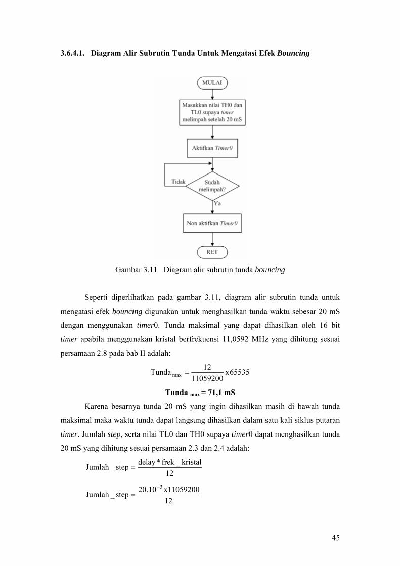
3.6.4.1. Diagram Alir Subrutin Tunda Untuk Mengatasi Efek Bouncing
Gambar 3.11 Diagram alir subrutin tunda bouncing
Seperti diperlihatkan pada gambar 3.11, diagram alir subrutin tunda untuk
mengatasi efek bouncing digunakan untuk menghasilkan tunda waktu sebesar 20 mS
dengan menggunakan timer0. Tunda maksimal yang dapat dihasilkan oleh 16 bit
timer apabila menggunakan kristal berfrekuensi 11,0592 MHz yang dihitung sesuai
persamaan 2.8 pada bab II adalah:
65535x11059200
12Tunda max =
Tunda max = 71,1 mS
Karena besarnya tunda 20 mS yang ingin dihasilkan masih di bawah tunda
maksimal maka waktu tunda dapat langsung dihasilkan dalam satu kali siklus putaran
timer. Jumlah step, serta nilai TL0 dan TH0 supaya timer0 dapat menghasilkan tunda
20 mS yang dihitung sesuai persamaan 2.3 dan 2.4 adalah:
12kristal_frek*delaystep_Jumlah =
1211059200x10.20step_Jumlah
3−=
45

Jumlah _step ≈ 18432d atau 4800h
THx/TLx = FFFFh – Jumlah_step (hexa) + 1h
TH0/TL0 = FFFFh – 4800h +1h
TH0/TL0 = B800h
3.6.4.2. Diagram Alir Subrutin Pengubahan Arah Putar Motor
Subrutin pengubahan arah putar motor digunakan untuk mengubah arah
putaran motor dari CW (searah jarum jam) menjadi CCW (berlawanan arah jarum
jam) atau sebaliknya. Seperti terlihat pada gambar 3.12, pengubahan arah cukup
dilakukan dengan mengkomplemenkan kondisi bit arah1. Karena pengubahan motor
dapat dilakukan ketika motor sedang berputar maka kecepatan motor perlu dikurangi
secara perlahan-lahan sampai akhirnya berhenti, sebelum dibalik arah putarnya.
Setelah itu, kecepatan motor juga perlu dinaikkan kembali secara perlahan-lahan
sampai mencapai nilai PWM yang diinginkan user. Hal ini dilakukan untuk
mengurangi sentakan akibat motor berhenti dan berakselerasi secara mendadak.
Gambar 3.12 Diagram alir subrutin pengubahan arah putar motor
46
3.6.5. Interupsi Pendeteksian Remote Control
Hal utama yang harus diperhatikan dalam pendeteksian remote control adalah
sinyal yang diterima oleh mikrokontroler dari IR receiver module merupakan
komplemen atau kebalikan dari sinyal yang dipancarkan oleh remote control. Selain
itu, pengkodean yang digunakan oleh remote control Sony adalah pengkodean lebar
pulsa atau pulse width codification. Pada pengkodean ini, bit ”1” direpresentasikan
dengan pulsa high selama 1200 μS diikuti pulsa low selama 600 μS. Sementara bit ”0”
direpresentasikan dengan dengan pulsa high selama 600 μS diikuti pulsa low selama
600 μS seperti terlihat pada gambar 2.20.
Protokol SIRC yang digunakan oleh remote control Sony untuk mengirimkan
data terdiri atas start bit yang berupa pulsa high selama 2,4 mS diikuti oleh jeda pulsa
low selama 600 μS, diikuti data yang berupa 7-bit command, dan 5-bit device address
seperti terlihat pada gambar 2.21. Pada gambar 3.13 diperlihatkan diagram alir
pendeteksian remote control.
Untuk menangkap kedua belas data yang dikirimkan, mikrokontroler
menggunakan dua buah variabel yakni var1 dan var2. Variabel var1 diset dengan nilai
00001000b, dan var2 dengan nilai 00000000b. Data yang diterima akan digeser ke
kanan satu per satu ke var1 + var2. Mikrokontroler akan mengetahui bahwa data yang
diterima telah berjumlah 12 dengan melihat kondisi bit carry. Setelah 12 kali
pergeseran maka bit carry akan berlogika ”1” karena bit ke tiga var1 yang diset high
telah masuk ke carry setelah bergeser melalui var1 + var2 sebanyak 12 kali.
Proses pendeteksian dipicu oleh terjadinya perubahan kondisi logika 1INT
dari kondisi idle-nya yaitu high, menjadi low, yang disebabkan adanya transmisi data
dari remote control. Kondisi picuan transisi negatif (negative edge) tersebut diset
dengan cara memberi logika high bit IT1 pada saat inisialisasi program. Perubahan
kondisi dari high menjadi low juga merupakan pertanda sedang dikirimkannya start
bit selama 2,4 mS dari remote control. Oleh karena itu mikrokontroler perlu
menunggu selama kira-kira 2,45 mS sebelum melakukan pengecekan ulang kondisi
bit 1INT atau pin 3.3. Apabila tidak maka langsung keluar dari subrutin dan kembali
ke program utama sementara apabila sinyal naik maka lanjutkan ke langkah
selanjutnya.
Langkah berikutnya, program akan menunggu sampai sinyal kembali turun.
Pada saat sinyal turun inilah saat yang paling penting dalam pendeteksian.
47

Mikrokontroler akan menunggu selama 900 μS atau 1,5 x 600 μS sebelum mengecek
kembali kondisi pin 3.3. Apabila kondisinya berubah menjadi high maka data yang
dikirimkan adalah ”0”. Sementara apabila kondisinya tetap low maka data yang
dikirimkan adalah ”1”.
Gambar 3.13 Diagram alir interupsi pendeteksian remote control
48

Gambar 3.13 (lanjutan) Diagram alir interupsi pendeteksian remote control
49
Untuk menuliskan ke dalam memori bahwa kondisi pin INT1 berubah menjadi
high yang berarti mikrokontroler menerima data ”0”, maka mikrokontroler akan
melakukan urutan langkah sebagai berikut:
1. Clear-kan bit carry, yang menunjukkan data yang diterima adalah ”0”.
2. Rotasikan ke kanan dengan menyertakan carry (Rotate right with carry) variabel
var1. Akibat dari instruksi ini maka carry akan masuk ke MSB var1, dan LSB
var1 akan masuk ke carry.
3. Rotasikan ke kanan dengan menyertakan carry (Rotate right with carry) variabel
var2. Akibat dari instruksi ini maka carry dari LSB var1 akan masuk ke MSB
var2, dan LSB var2 akan masuk ke carry.
4. Kemudian dilakukan pengecekan bit carry apakah telah bernilai ”1”, yang berarti
telah menerima 12 data? Apabila ya, maka program akan merotasikan ke kanan
var1 + var2 untuk menempatkan 7 bit command di var2, dan 5 bit device address
di var1. Apabila tidak, maka program akan kembali untuk mengecek kondisi
sinyal di 3.3 apakah telah berubah menjadi low.
Sementara untuk menuliskan ke dalam memori bahwa kondisi pin 3.3 tetap
low yang berarti mikrokontroler menerima data ”1”, maka mikrokontroler akan
melakukan urutan langkah yang hampir sama dengan apabila kondisi pin 3.3 berubah
high. Perbedaan antara keduanya adalah pada bagian ini carry diset high untuk
mengindikasikan data yang diterima adalah”1”, serta branching program saat total
data yang diterima belum mencapai 12 bit. Program akan mengarah setingkat lebih
tinggi dari penjelasan algoritma sebelumnya yakni program harus mengecek apakah
kondisi pin 3.3 telah berubah menjadi high kembali.
Tabel 3.3. Perancangan fungsi dari tombol remote control yang ditekan
Tombol Command code Fungsi
Vol + 12h Naikkan PWM1 sebesar 1%
Vol - 13h Turunkan PWM1 sebesar 1%
Normal 16h Ubah arah motor 1
Prog + 10h Naikkan PWM2 sebesar 1%
Prog - 11h Turunkan PWM2 sebesar 1%
Select - 75h Ubah arah motor 2
Setelah ketujuh bit command tersimpan di dalam variabel var1 maka
dilakukan pendeteksian tombol mana yang ditekan oleh user. Pada perancangan ini
50

hanya 6 tombol yang akan digunakan. Keenam tombol beserta fungsinya dapat dilihat
pada tabel 3.3. Kemudian dilakukan pemanggilan subrutin kirim data ke
mikrokontroler sekunder. Setelah itu dilakukan kembali pengaktifan kembali fungsi
interupsi eksternal yang pada awal proses pendeteksian ini dinonaktifkan.
3.6.5.1 Diagram Alir Subrutin Tunda 2,45 mS
Diagram alir subrutin tunda 2,45 mS diperlihatkan pada gambar 3.14. Karena
besarnya tunda 2,45 mS yang ingin dihasilkan masih dibawah tunda maksimal sebesar
71,7 mS maka tunda dapat langsung dihasilkan dalam satu kali siklus putaran timer.
Dengan menggunakan persamaan 2.9 dan 2.10, dapat dihitung jumlah step, serta nilai
TL0 dan TH0 yang harus dimasukkan supaya timer0 dapat menghasilkan tunda
sebesar 2,45 mS , yaitu:
12kristal_frek*delaystep_Jumlah =
1211059200x10.45,2step_Jumlah
3−=
Jumlah _step ≈ 2257d atau 08D1h
THx/TLx = FFFFh – Jumlah_step + 1h
TH0/TL0 = FFFFh – 08D1h +1h
TH0/TL0 = F72Fh
Gambar 3.14 Diagram alir subrutin tunda 2,45 mS
51

Subrutin diagram alir untuk menghasilkan tunda 0,9 mS hampir sama dengan
diagram alir subrutin tunda 2,45 mS. Perbedaan hanya terdapat pada hasil perhitungan
untuk menentukan nilai TL0 dan TH0, yaitu: C3h untuk TL0, dan FCh untuk TH0.
3.6.6. Interupsi Scanning Seven-Segment
Seperti ditunjukkan pada gambar 3.15, diagram alir interupsi scanning seven-
segment diawali dengan mematikan semua seven-segment. Kemudian diikuti dengan
menunjuk alamat data yang akan ditampilkan dan mengkonversikannya sesuai dengan
posisi pin seven-segment. Setelah itu, tunjuk dan aktifkan seven-segment yang sesuai.
Seandainya ini merupakan data terakhir, maka alamat data dan posisi seven-segment
perlu di reset ke alamat awal, kalau tidak maka alamat data dan posisi baru harus
disimpan. Proses scanning ini akan dipicu oleh interupsi timer1 yang terjadi setiap 2,5
mS.
Gambar 3.15 Diagram alir tampilan seven-segment
52

3.6.6.1 Diagram alir Subrutin Pengubahan Data dari Heksa Desimal Menjadi
BCD
Subrutin pengubahan data dari bilangan heksa desimal menjadi BCD (Binary
Coded Decimal) dilaksanakan oleh mikrokontroler setiap kali mikrokontroler selesai
menerima data masukan, baik dari tombol push-button maupun dari remote control.
Diagram alirnya diperlihatkan pada gambar 3.16. Pada bagian ini data yang akan
diubah menjadi bilangan BCD adalah data yang tersimpan pada PWM1 dan PWM2
yang tersimpan pada alamat memori 30h dan 31h. Nilai BCD ini kemudian akan
digunakan sebagai nilai indexed addressing pada look-up table yang menunjukkan
tampilan seven- segment yang sesuai.
Setelah itu data arah_mtr yang tersimpan pada alamat 32H akan dicek untuk
untuk mengetahui arah putar motor pertama dan kedua. Apabila arah putar motor
adalah CW maka nilai indexed adressing-nya adalah 10 yang akan menampilkan
tulisan pada seven-segment. Sedangkan apabila arah putarnya adalah CCW maka
nilai indexed adressing-nya adalah 11 yang akan menampilkan tulisan pada seven-
segment .
Prinsip pengubahan bilangan heksa desimal menjadi BCD adalah sebagai
berikut (pada perancangan ini, proses dibatasi hanya untuk bilangan desimal antara 0d
sampai 100d atau 00h sampai 64h pada bilangan heksa desimal) :
1. Cek apakah nibble (4 bit) bawah sama atau lebih besar dari 10d? Apabila ya
tambahkan dengan 6 dan set carry, kemudian simpan sebagai digit satuan. Apabila
tidak maka langsung disimpan tanpa perlu dilakukan penambahan.
2. Ambil nibble atas dan cek apakah terdapat carry dari proses sebelumnya? Kalau
ya maka tambahkan satu dan apabila tidak maka tidak perlu ditambah. Kemudian
cek apakah nilai setelah penambahan lebih besar atau sama dengan 10d? Apabila
ya tambahkan dengan 6 dan set carry, kemudian simpan sebagai digit puluhan.
Apabila tidak maka langsung disimpan tanpa perlu dilakukan penambahan.
Diagram alir proses pengecekan dan pengubahan tiap nibble dapat dilihat pada
gambar 3.17.
53

Gambar 3.16 Diagram alir subrutin pengubahan data dari heksa desimal menjadi BCD
54

Gambar 3.17 Diagram alir subrutin pengecekan dan pengubahan nibble.
55
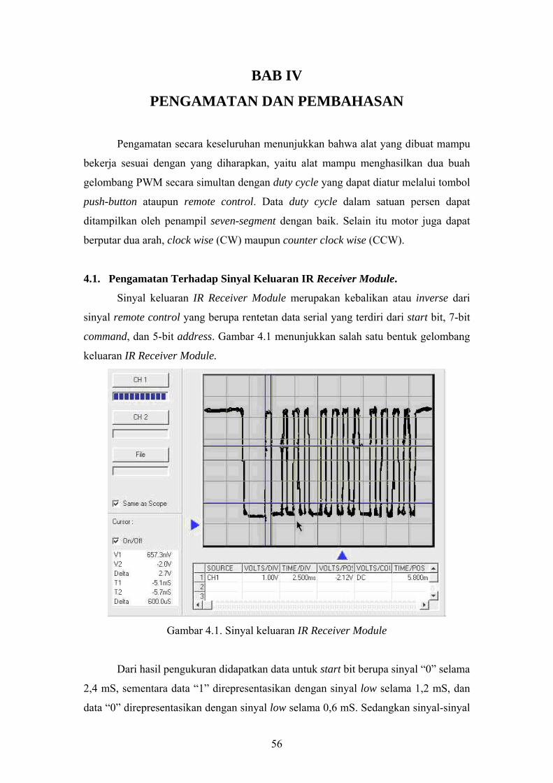
BAB IV
PENGAMATAN DAN PEMBAHASAN
Pengamatan secara keseluruhan menunjukkan bahwa alat yang dibuat mampu
bekerja sesuai dengan yang diharapkan, yaitu alat mampu menghasilkan dua buah
gelombang PWM secara simultan dengan duty cycle yang dapat diatur melalui tombol
push-button ataupun remote control. Data duty cycle dalam satuan persen dapat
ditampilkan oleh penampil seven-segment dengan baik. Selain itu motor juga dapat
berputar dua arah, clock wise (CW) maupun counter clock wise (CCW).
4.1. Pengamatan Terhadap Sinyal Keluaran IR Receiver Module.
Sinyal keluaran IR Receiver Module merupakan kebalikan atau inverse dari
sinyal remote control yang berupa rentetan data serial yang terdiri dari start bit, 7-bit
command, dan 5-bit address. Gambar 4.1 menunjukkan salah satu bentuk gelombang
keluaran IR Receiver Module.
Gambar 4.1. Sinyal keluaran IR Receiver Module
Dari hasil pengukuran didapatkan data untuk start bit berupa sinyal “0” selama
2,4 mS, sementara data “1” direpresentasikan dengan sinyal low selama 1,2 mS, dan
data “0” direpresentasikan dengan sinyal low selama 0,6 mS. Sedangkan sinyal-sinyal
56

high selama 0,6 mS merupakan sinyal idle. Pengamatan ini menunjukkan bahwa data
yang dikeluarkan oleh IR Receiver Module sesuai dengan pengkodean lebar pulsa
SIRC SONY yang tertulis di dasar teori. Tabel 4.1 memperlihatkan fungsi-fungsi
tombol remote control untuk mengendalikan perangkat digital laser show.
Tabel 4.1. Fungsi dari tombol remote control yang ditekan
Tombol Command code Fungsi Keterangan
Vol + 12h Naikkan PWM1 sebesar 1% Sesuai perancangan
Vol - 13h Turunkan PWM1 sebesar 1% Sesuai perancangan Normal 16h Ubah arah motor 1 Sesuai perancangan Prog + 10h Naikkan PWM2 sebesar 1% Sesuai perancangan Prog - 11h Turunkan PWM2 sebesar 1% Sesuai perancangan
Select - 75h Ubah arah motor 2 Sesuai perancangan
4.2. Pengamatan terhadap pulsa PWM
Pulsa PWM diamati pada bagian keluaran non-inverting buffer 74hc541 yang
dihubungkan ke ground melalui sebuah resistor 1kΩ. Masukan dari buffer berasal dari
port 1.0 dan 1.1 mikrokontroler AT89S51 yang difungsikan sebagai output. Bentuk
gelombang sinyal PWM dengan duty cycle 63% dapat diamati pada gambar 4.2.
Gambar 4.2 Bentuk pulsa PWM dengan duty cycle 63%
Dari hasil pengamatan gambar diatas terlihat bahwa bentuk gelombang
keluaran sinyal PWM berupa gelombang kotak dengan frekuensi yang berkisar antara
91,75 Hz sampai 92,65 Hz. Duty cycle yang terukur dari osiloskop digital
57

menunjukkan range data antara 62, 65% sampai 63,76%. Frekuensi dan duty cycle
yang berubah-ubah tersebut dikarenakan interupsi timer 0 untuk melakukan scanning
seven-segment.
Pada tabel 4.2 disajikan data pengamatan terhadap beberapa contoh pulsa
PWM dengan duty cycle yang berbeda-beda. Dari tabel dapat terlihat bahwa range
error untuk duty cycle PWM yang berbeda-beda memiliki nilai yang hampir sama. Ini
menunjukkan bahwa penginterupsian oleh program scanning seven-segment
dilakukan secara periodis dan teratur. Perbedaan yang terjadi disebabkan oleh
kekurangtelitian alat pengukur saat mencuplik data. Rerata range error PWM pertama
adalah sebesar 0,77%. Sedangkan rerata untuk PWM kedua adalah sebesar 0,71%.
Tabel 4.2. Data pengamatan duty cycle PWM
Motor 1 Motor 2
PWM teramati
(%)
PWM teramati
(%)
PWM
set point
(%) Batas
bawah
Batas
atas
Range Error
(%) Batas
bawah
Batas
atas
Range Error
(%)
0 0 0 0 0 0 0
1 0,90 1,1 0,2 0,91 1,2 0,29
10 9,58 10,35 0,77 9,28 10,11 0,83
20 19,65 20,45 0,8 19,48 20,35 0,87
30 29,73 30,56 0,83 29,61 30,38 0,77
40 39,73 40,55 0,82 39,80 40,37 0,58
50 49,67 50,38 0,71 49,58 50,48 0,9
60 59,51 60,45 0,94 59,58 60,61 1,03
70 69,65 70,63 0,98 69,71 70,37 0,66
80 79,52 80,61 1,09 79,65 80,54 0,89
90 89,45 90,62 1,17 89,84 90,68 0,84
99 98,34 99,28 0,94 98,21 99,11 0,9
Rerata range error 0,77 Rerata range error 0,71
Ket: Range error didapatkan dengan mengurangkan batas atas dengan batas bawah.
Range error = batas atas - batas bawah
Rerata range error didapatkan dengan menjumlahkan semua sample data range
error dan membaginya dengan jumlah sample.
58

4.3. Hubungan kecepatan putar motor dengan presentase PWM
Kecepatan putar masing-masing motor diukur dengan menggunakan
tachometer baik pada saat berputar searah (CW) maupun berlawanan (CCW) jarum
jam. Metodenya adalah dengan menempelkan kertas berwarna gelap (hitam) ke
sekeliling cermin sehingga menyerupai tabung, kemudian pada salah satu bagian
tabung tersebut ditempelkan selapis kertas reflektor untuk memantulkan kembali sinar
yang dipancarkan tachometer yang akan digunakan sebagai input counter tachometer.
Hasil pengukuran menggunakan tachometer terhadap kecepatan motor
disajikan dalam tabel 4.3 sampai 4.6. Sedangkan tampilan grafiknya disajikan mulai
gambar 4.3 sampai 4.6. Dari hasil pengukuran dapat diamati bahwa peningkatan
kecepatan motor berupa kurva logaritmis dibandingkan dengan kenaikan presentase
PWM yang linear. Hal ini diakibatkan oleh karakteristik motor yang tidak linear.
Pada pengamatan kecepatan minimal motor dapat dilihat bahwa motor dapat
masih dapat berputar pada tingkat PWM 6% apabila kecepatannya diturunkan dari
kecepatan yang lebih tinggi. Sedangkan apabila dari diam, motor akan mulai berputar
pada presentase PWM sebesar 9%. Perbedaan ini dikarenakan gaya kelembaman,
yaitu suatu gaya yang menyebabkan suatu benda akan cenderung mempertahankan
kondisi terakhirnya sehingga diperlukan energi yang lebih besar untuk merubah
kondisi tersebut. Secara umum dapat dianalisa bahwa karakteristik starting point
motor cukup bagus karena berada pada titik yang cukup rendah.
Pengamatan untuk membandingkan karakteristik kedua motor menunjukkan
bahwa kedua motor memiliki karakteristik yang hampir sama dilihat dari starting
point minimum, maupun grafik perubahan kecepatannya. Perbedaan antara kedua
motor terletak pada kecepatan maksimal motor pertama yang lebih rendah daripada
motor kedua.
Sedangkan pengamatan untuk melihat perbedaan kecepatan saat motor
berputar searah (CW) dan berlawanan (CCW) jarum jam memperlihatkan bahwa
kecepatan motor saat berputar searah jarum jam sedikit lebih cepat dibanding
sebaliknya. Hal ini dikarenakan kedua motor yang digunakan adalah jenis motor CW,
yang berarti didesain untuk bekerja lebih optimal saat berputar searah jarum jam.
Namun sesuai karakteristik motor DC yang akan berubah arah apabila polaritas
tegangannya dibalik, motor-motor ini juga mampu berputar CCW dengan cukup baik.
59

Tabel 4.3 Kecepatan motor 1 saat berputar searah jarum jam (CW)
PWM
(%)
Kec.
(RPM)
PWM
(%)
Kec.
(RPM)
PWM
(%)
Kec.
(RPM)
PWM
(%)
Kec.
(RPM)
PWM
(%)
Kec.
(RPM)
0 0 20 2735 40 3701 60 3978 80 4180
1 0 21 2835 41 3726 61 3988 81 4189
2 0 22 2901 42 3747 62 4003 82 4195
3 0 23 2975 43 3752 63 4016 83 4199
4 0 24 3045 44 3769 64 4035 84 4205
5 0 25 3140 45 3779 65 4050 85 4210
6 298 26 3198 46 3801 66 4064 86 4212
7 679 27 3238 47 3822 67 4079 87 4214
8 972 28 3259 48 3838 68 4085 88 4216
9 1297 29 3285 49 3859 69 4096 89 4217
10 1531 30 3299 50 3870 70 4101 90 4219
11 1702 31 3341 51 3895 71 4105 91 4220
12 1903 32 3389 52 3920 72 4111 92 4222
13 2069 33 3425 53 3931 73 4118 93 4225
14 2189 34 3486 54 3950 74 4123 94 4227
15 2276 35 3508 55 3956 75 4125 95 4230
16 2386 36 3567 56 3966 76 4138 96 4233
17 2509 37 3612 57 3969 77 4147 97 4237
18 2604 38 3656 58 3974 78 4161 98 4245
19 2686 39 3684 59 3977 79 4171 99 4248
MOTOR 1 CW
0
1000
2000
3000
4000
5000
1 6 11 16 21 26 31 36 41 46 51 56 61 66 71 76 81 86 91 96
PWM (%)
RPM
Gambar 4.3 Hubungan kecepatan putar searah jarum jam (CW) motor 1 terhadap
presentase PWM
60

Tabel 4.4. Kecepatan motor 1 saat berputar berlawanan jarum jam (CCW) PWM
(%)
Kec.
(RPM)
PWM
(%)
Kec.
(RPM)
PWM
(%)
Kec.
(RPM)
PWM
(%)
Kec.
(RPM)
PWM
(%)
Kec.
(RPM)
0 0 20 2728 40 3694 60 3970 80 4166
1 0 21 2829 41 3718 61 3976 81 4178
2 0 22 2894 42 3740 62 3985 82 4182
3 0 23 2970 43 3742 63 4001 83 4185
4 0 24 3031 44 3760 64 4022 84 4191
5 0 25 3131 45 3767 65 4037 85 4196
6 295 26 3190 46 3791 66 4049 86 4200
7 610 27 3229 47 3818 67 4055 87 4201
8 910 28 3251 48 3830 68 4059 88 4201
9 1265 29 3275 49 3851 69 4075 89 4206
10 1465 30 3289 50 3861 70 4086 90 4209
11 1645 31 3332 51 3887 71 4091 91 4211
12 1896 32 3381 52 3916 72 4097 92 4213
13 2068 33 3415 53 3925 73 4101 93 4215
14 2159 34 3475 54 3941 74 4109 94 4218
15 2270 35 3501 55 3951 75 4111 95 4221
16 2381 36 3561 56 3958 76 4120 96 4224
17 2500 37 3604 57 3961 77 4134 97 4235
18 2508 38 3648 58 3964 78 4146 98 4238
19 2678 39 3678 59 3968 79 4157 99 4239
MOTOR 1 CCW
0
1000
2000
3000
4000
5000
1 6 11 16 21 26 31 36 41 46 51 56 61 66 71 76 81 86 91 96
PWM (%)
RPM
Gambar 4.4. Hubungan kecepatan putar berlawanan jarum jam (CCW) motor 1
terhadap presentase PWM
61

Tabel 4.5. Kecepatan motor 2 saat berputar searah jarum jam (CW) PWM
(%)
Kec.
(RPM)
PWM
(%)
Kec.
(RPM)
PWM
(%)
Kec.
(RPM)
PWM
(%)
Kec.
(RPM)
PWM
(%)
Kec.
(RPM)
0 0 20 2855 40 3861 60 4218 80 4395
1 0 21 2921 41 3890 61 4223 81 4402
2 0 22 2999 42 3929 62 4236 82 4412
3 0 23 3132 43 3948 63 4247 83 4423
4 0 24 3150 44 3956 64 4252 84 4435
5 0 25 3211 45 3971 65 4263 85 4445
6 334 26 3244 46 4006 66 4275 86 4450
7 683 27 3291 47 4035 67 4286 87 4455
8 990 28 3332 48 4045 68 4291 88 4467
9 1315 29 3372 49 4046 69 4299 89 4479
10 1558 30 3470 50 4066 70 4301 90 4482
11 1785 31 3520 51 4120 71 4310 91 4498
12 1963 32 3615 52 4123 72 4329 92 4511
13 2120 33 3640 53 4131 73 4324 93 4518
14 2244 34 3684 54 4178 74 4345 94 4521
15 2343 35 3703 55 4181 75 4362 95 4524
16 2473 36 3740 56 4199 76 4355 96 4531
17 2590 37 3770 57 4205 77 4375 97 4546
18 2685 38 3780 58 4210 78 4385 98 4551
19 2787 39 3839 59 4213 79 4389 99 4550
MOTOR 2 CW
0
1000
2000
3000
4000
5000
1 6 11 16 21 26 31 36 41 46 51 56 61 66 71 76 81 86 91 96
PWM (%)
RPM
Gambar 4.5. Hubungan kecepatan putar searah jarum jam (CW) motor 2 terhadap
presentase PWM
62

Tabel 4.6. Kecepatan motor 2 saat berputar berlawanan jarum jam (CCW) PWM
(%)
Kec.
(RPM)
PWM
(%)
Kec.
(RPM)
PWM
(%)
Kec.
(RPM)
PWM
(%)
Kec.
(RPM)
PWM
(%)
Kec.
(RPM)
0 0 20 2803 40 3831 60 4205 80 4363
1 0 21 2868 41 3849 61 4209 81 4378
2 0 22 2933 42 3980 62 4212 82 4386
3 0 23 3056 43 3910 63 4221 83 4391
4 0 24 3109 44 3919 64 4230 84 4397
5 0 25 3168 45 3942 65 4240 85 4405
6 305 26 3215 46 3967 66 4253 86 4416
7 643 27 3244 47 4001 67 4261 87 4423
8 964 28 3284 48 4010 68 4275 88 4431
9 1342 29 3325 49 4038 69 4286 89 4439
10 1501 30 3412 50 4059 70 4293 90 4445
11 1635 31 3472 51 4086 71 4299 91 4456
12 1841 32 3543 52 4091 72 4302 92 4469
13 2033 33 3610 53 4110 73 4310 93 4479
14 2204 34 3641 54 4132 74 4318 94 4492
15 2311 35 3662 55 4153 75 4329 95 4499
16 2421 36 3686 56 4163 76 4336 96 4502
17 2512 37 3741 57 4179 77 4347 97 4511
18 2652 38 3769 58 4185 78 4351 98 4517
19 2754 39 3799 59 4199 79 4356 99 4523
MOTOR 2 CCW
0
1000
2000
3000
4000
5000
1 6 11 16 21 26 31 36 41 46 51 56 61 66 71 76 81 86 91 96
PWM (%)
RPM
Gambar 4.6 Hubungan kecepatan putar berlawanan jarum jam (CCW) motor 2
terhadap presentase PWM
63

4.4. Hubungan PWM, Kecepatan Motor, dan Pola Yang Dihasilkan
Pola yang dihasilkan pada saat kedua motor diputar pada arah searah jarum
jam ditunjukkan pada tabel 4.7. Pada saat kedua motor dibalik arah putarnya menjadi
CCW, dengan nilai PWM yang sama seperti tabel 4.7, ternyata pola yang dihasilkan
juga sama. Oleh karena itu tabel 4.7 dapat dikatakan menggambarkan pola yang
terbentuk saat kedua motor berputar searah.
Sedangkan pola yang dihasilkan saat motor pertama diputar searah jarum jam
(CW) dan motor 2 diputar berlawanan jarum jam (CCW) disajikan dalam tabel 4.8.
Pada saat motor pertama dibalik arah putarnya menjadi CCW, dan motor kedua yang
menjadi CW, ternyata pola yang dihasilkan adalah sama untuk nilai PWM yang sama.
Sehingga tabel 4.8 dapat mewakili pola yang terbentuk saat kedua motor berputar
berlawanan arah.
Tabel 4.7. Pola yang terbentuk saat kedua motor berputar searah
PWM1 (%) CW PWM2 (%) CW Kec. M1 (rpm) Kec. M2 (rpm) Pola
0 0 0 0
10 0 1531 0
10 10 1531 1558
10 21 1531 2921
10 40 1531 3861
17 82 2509 4412
20 87 2735 4455
69 11 4096 1785
70 17 4101 2590
97 09 4237 1315
65 15 4050 2343
24 08 3045 990
64
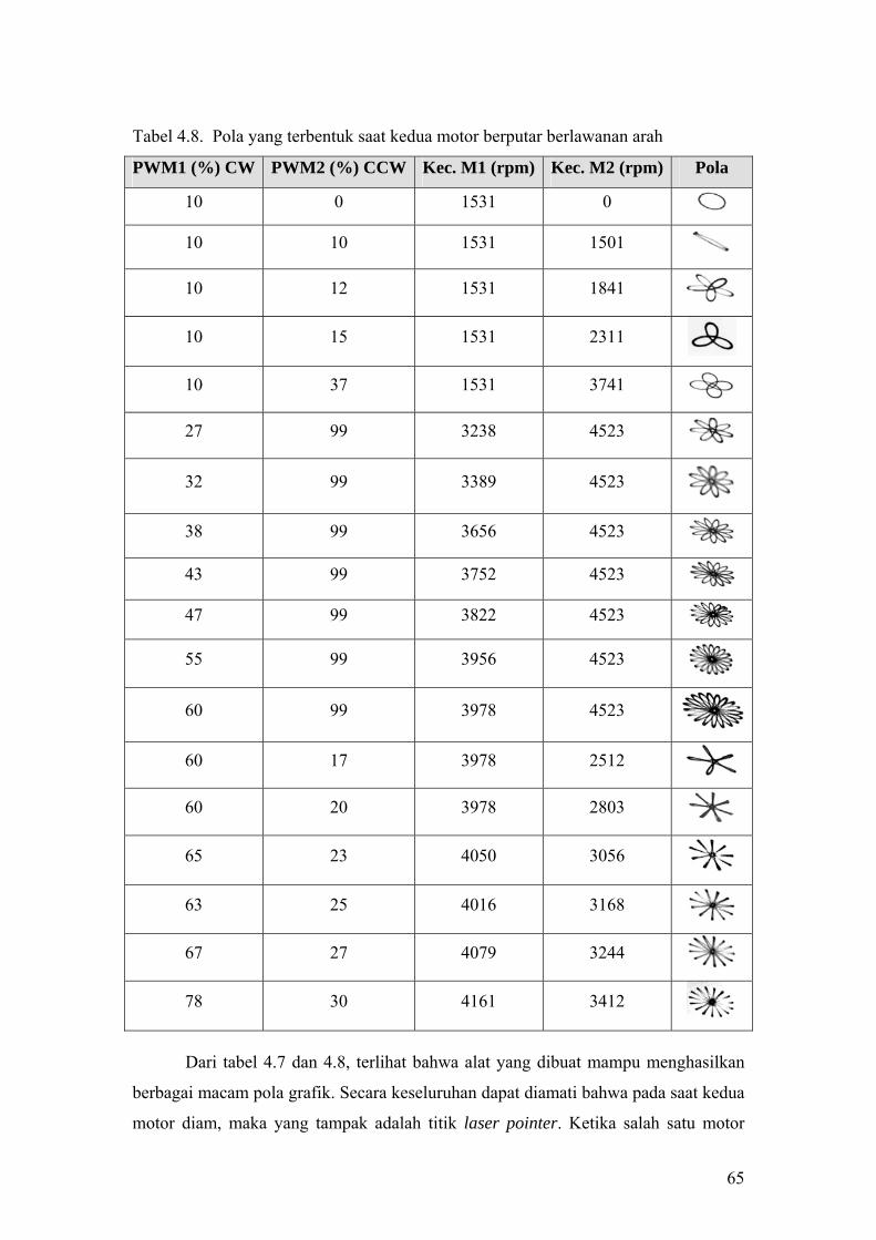
Tabel 4.8. Pola yang terbentuk saat kedua motor berputar berlawanan arah
PWM1 (%) CW PWM2 (%) CCW Kec. M1 (rpm) Kec. M2 (rpm) Pola
10 0 1531 0
10 10 1531 1501
10 12 1531 1841
10 15 1531 2311
10 37 1531 3741
27 99 3238 4523
32 99 3389 4523
38 99 3656 4523
43 99 3752 4523
47 99 3822 4523
55 99 3956 4523
60 99 3978 4523
60 17 3978 2512
60 20 3978 2803
65 23 4050 3056
63 25 4016 3168
67 27 4079 3244
78 30 4161 3412
Dari tabel 4.7 dan 4.8, terlihat bahwa alat yang dibuat mampu menghasilkan
berbagai macam pola grafik. Secara keseluruhan dapat diamati bahwa pada saat kedua
motor diam, maka yang tampak adalah titik laser pointer. Ketika salah satu motor
65

berputar maka keluarannya berbentuk lingkaran. Apabila kedua motor berputar pada
arah yang sama maka akan terbentuk lingkaran minor yang mengarah ke dalam
lingkaran utama.
Sedangkan apabila gerakan kedua motor berlawanan, dengan kecepatan motor
pertama lebih rendah dibanding motor kedua maka akan terlihat lingkaran minor
cembung yang mengarah keluar dan berbentuk seperti bidang polar. Dan apabila
kecepatan motor pertama lebih besar dibanding motor kedua maka akan terlihat
lingkaran minor pipih yang mengarah keluar dan berbentuk menyerupai bentuk
bintang.
Jumlah lingkaran minor yang terbentuk, maupun arah gerakannya dipengaruhi
oleh perbandingan kecepatan antara motor pertama dan kedua. Gambar yang kurang
jelas disebabkan karena intensitas sinar laser yang tidak cukup terang, dan
kemampuan kamera yang tidak mampu merekam dengan kecepatan tinggi serta
kemampuan lensa kamera yang lebih lemah dibandingkan lensa mata.
4.5. Bentuk fisik alat
(a)
(b)
Gambar 4.7. Bentuk fisik alat
(a) Tampak depan (b) Tampak sudut samping kiri atas dengan tutup terbuka
Seperti terlihat pada gambar 4.7, alat yang dibuat kemudian dikemas dengan
menggunakan bahan isolator yang terbuat dari acrylic yang kokoh sehingga cukup
66

aman untu menjaga rangkaian di dalamnya dari kerusakan akibat benturan serta
mengamankan user dari bahaya tersengat arus listrik. Bahan acrylic yang tembus
pandang juga memungkinkan sinar infra merah dari remote control dapat diterima
dengan baik oleh IR Receiver Module yang berada di dalam kotak. Demikian pula
pantulan sinar laser dapat dengan mudah diteruskan sebelum tertampil di dinding.
Kemasan yang tembus pandang juga menambah daya tarik perangkat ini
sebagai sarana hiburan, karena user dapat melihat keseluruhan rangkaian elektronis
maupun mekanik, serta mengamati proses dan cara kerja perangkat ini. Keterangan
fungsi yang menyertai masing-masing tombol diharapkan akan memudahkan user
dalam mengoperasikan perangkat ini. Dengan desain yang kompak dan portable,
perangkat ini akan lebih mudah untuk dibawa maupun dipindahkan.
4.6. Penempatan mekanis motor, cermin, dan laser
Seperti terlihat pada gambar 4.8, cermin dipasangkan pada rotor masing-
masing motor pada titik tengah cermin. Apabila motor berputar maka cermin juga
akan berputar dengan sedikit bergoyang karena adanya kerenggangan antar rotor dan
stator. Putaran motor akan menyebabkan gaya gravitasi yang dialami oleh cermin
membuat cermin sedikit terpantul-pantul yang terlihat seperti bergoyang. Goyangan
pada cermin akan menyebabkan terbentuknya pola-pola grafis apabila terdapat sinar
terpantul dari bidang permukaan cermin.
Motor 1
Motor 2Laser
pointer
Cermin
Cermin
Pantulan ke layar
Gambar 4.8. Penempatan mekanis motor, cermin, dan laser
67

Posisi kedua motor dipasang pada posisi berhadap-hadapan dan diatur
jaraknya sedemikan rupa sehingga pantulan sinar laser dari cermin pertama dapat
mengenai dan terpantulkan kembali dengan sempurna oleh motor kedua ke layar.
Laser pointer juga harus terpasang dengan posisi dan sudut yang tepat sehingga
mampu terpantul dengan sempurna oleh kedua cermin. Pengaturan posisi dan jarak
yang tidak tepat diantara ketiganya akan menyebabkan sinar laser tidak dapat
terpantul seutuhnya ketika motor berputar. Hal ini dikarenakan ketika cermin
bergoyang maka akan terbentuk sudut pada bidang pantulan yang menyebabkan lebar
bidang pantulan semakin lebar dan memungkinkan sebagian pantulan tidak mengenai
salah satu atau kedua cermin. Apabila ini terjadi maka pola yang terbentuk akan
menjadi cacat atau terpotong.
68

BAB V
KESIMPULAN DAN SARAN
5.1. Kesimpulan
Secara umum dapat disimpulkan bahwa alat yang dibuat mampu memenuhi
tujuan yang diinginkan yaitu untuk menghasilkan suatu perangkat digital laser show
dengan metode pemantulan terhadap cermin berputar yang kecepatan dan arahnya
dapat dikendalikan secara digital. Secara lebih spesifik, dari penelitian didapatkan
hasil sebagai berikut:
1. Perangkat dibuat mampu menghasilkan pola-pola yang beraneka ragam.
2. Semakin banyak cermin yang berputar semakin banyak pula macam pola yang
dapat dihasilkan.
3. Semakin banyak kombinasi kecepatan dan arah putar motor semakin banyak
pula pola yang dihasilkan.
4. Kecepatan dua motor dapat diatur dengan metode PWM dengan kenaikan atau
penurunan duty cycle setiap 1%, dengan rerata range error sebesar 0,77%
untuk PWM pertama dan 0,71% untuk PWM kedua.
5. Pengendalian kecepatan motor dapat dilakukan dengan lebih mudah karena
dapat dikendalikan secara nirkabel menggunakan IR Remote control.
5.2. Saran
Untuk pengembangan lebih lanjut penulis memberikan beberapa saran sebagai
berikut:
1. Untuk memperbanyak variasi pola dapat digunakan tiga atau lebih motor DC
sekaligus.
2. Untuk memudahkan mobilitas dapat digunakan power supply berupa baterai
atau accu.
3. Untuk menghasilkan gelombang PWM, dapat digunakan mikrokontroler yang
memberikan fasilitas PWM built-in di dalamnya.
69

DAFTAR PUSTAKA -----, Brushed Motor DC, Freescale Semiconductor Inc., 2004-2005.
(http://www.freescale.com/webapp/sps/site/overview.jsp?nodeId=02nQXGrrlPY7r8f7sz.htm)
-----, L293, L293D Quadruple Half-H Drivers, Texas Instruments, Texas, 2002 (http://www.focus.ti.com/docs/prod/folders/print/l293d.html)
-----, Lecture7. Digital display. (hibp.ecse.rpi.edu/~connor/education/ IEE/lectures/Lecture_7_digital_display.pdf)
-----, Lissajous curve, Wikimedia Foundation, Inc., 2007 (http://en.wikipedia.org/wiki/Lissajous_curve.htm)
-----, MC78XX/LM78XX/MC78XXA 3-Terminal 1A Positive Voltage Regulator, 2001.
(www.fairchildsemi.com)
-----, Seven-Segment Display, Answers.com (http://www.Answers.com/seven-segment-display.htm)
-----, PWM Signal Generators.
(http://homepages.which.net/~paul.hills/circuits/pwmgenerators/pwmgenerators.html)
Atmel, 8-bit Microcontroller with 4K Bytes In-System Programmable Flash: AT89S51,
Atmel Corp., 2001 (www.atmel.com/dyn/resources/prod_documents/doc2487.pdf)
Barr, Michael., Pulse Width Modulation, Embedded Systems Programming, 2001 (http://www.netrino.com/publications/glossary/pwm.htm)
Bergmans, San, IR Remote Control Theory, Oisterwijk, 2001
(http://www.slydiman.compass.com.ru/scr/kb/ir.htm)
Bergmans, San, Sony SIRC Protocol, Oisterwijk, 2003 (http://www. xs4all.nl/~sbp/knowledge/ir/sirc.htm)
Floyd, Thomas L., Electronic Devices Electron-Flow Version, Prentice Hall, Englewood Cliff, Second Edition, 1996
Harsono, Budianto, Pembangkit Pola Atraksi Sinar Laser, Teknik Elektro Universitas Sanata Dharma, Yogyakarta, 2005.
Lipnharski, Wagner, Remote Control Technical Specifications SONY, UST Research Inc., 2002 (http://www.ustr.net/infrared/sony.shtml)
McManis, Chuck, H-BRIDGES: Theory and Practice, 2003.
(www.mcmanis.com/chuck/robotics/tutorial/h-bridge)
70

Microsoft, Microsoft Encarta 2005: Laser, Microsoft Corp., 2004. Nalwan, Paulus Andi, Panduan Praktis Teknik Antar Muka dan Pemrograman
Mikrokontroler AT89C51, PT Elex Media Computindo, Jakarta, 2003.
Nave R., DC Motor Operation, HyperPhysics. (http://hyperphysics.phy-astr.gsu.edu/hbase/hframe.html)
Kunihiro, Matsuda, Seri Teknologi Tinggi Bergambar: LASER, PT Elex Media
Computindo, Jakarta, 1987.
Price, T. E., Analog Electronic: An Integrated Pspice approach, Prentice Hall Europe, Hemel Hemstead, 1997.
Putra, Agfianto Eko, Belajar Mikrokontroler AT89C51/52/55 (Teori dan Aplikasi), Gava Media, Yogyakarta, 2002.
Steiner, Craig, The 8052 Tutorial and Reference, Vault Information Services LLC, version 1.00, 2004.
Torrens, Richard, 4QD-TEC: Electronics Circuits Reference Archive PWM Speed Control, 4QD-TEC, 2004 (http://www.4qdtec.com/pwm-01.html)
Weisstein, Eric W, Hypotrochoid, Wolfram Research Inc., 2006
(http://mathworld.wolfram.com/Hypotrochoid.html)
Ibid, Hypocycloid, Wolfram Research Inc., 2006 (http://mathworld.wolfram.com/Hypocycloid.html)
Ibid, Rose, Wolfram Research Inc., 2006 (http://mathworld.wolfram.com/Rose.html)
71

LAMPIRAN
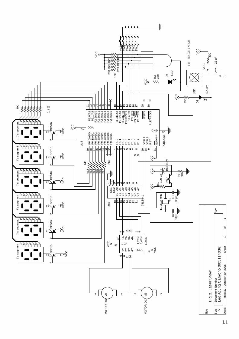
L1
180
Leo
Agun
g C
ahyo
no (0
0511
4036
)
Dig
ital L
aser
Sho
w
A
11
Mon
day
, O
ctob
er 3
0, 2
006
Title
Siz
eD
ocum
ent
Num
ber
Rev
Dat
e:S
heet
of
VC
C
U15
AT8
9C51
91819
20
29 30
31
40
1 2 3 4 5 6 7 8
21 22 23 24 25 26 27 28 10 11 12 13 14 15 16 17
39 38 37 36 35 34 33 32
RS
TXT
AL2
XTA
L1
GND
PS
EN
ALE
/PR
OG
EA
/VP
P
VCC
P1.
0P
1.1
P1.
2P
1.3
P1.
4P
1.5
P1.
6P
1.7
P2.
0/A
8P
2.1/
A9
P2.
2/A
10P
2.3/
A11
P2.
4/A
12P
2.5/
A13
P2.
6/A
14P
2.7/
A15
P3.
0/R
XDP
3.1/
TXD
P3.
2/IN
TOP
3.3/
INT1
P3.
4/TO
P3.
5/T1
P3.
6/W
RP
3.7/
RD
P0.
0/A
D0
P0.
1/A
D1
P0.
2/A
D2
P0.
3/A
D3
P0.
4/A
D4
P0.
5/A
D5
P0.
6/A
D6
P0.
7/A
D7
R17
2K2
7's
segm
ent 4 2 9167 10
3
330
22 u
F
+C
5
10uF
/16V
VC
C
BC
516
3
2
1VC
C
R3
330
VC
C
VC
C
C2
33pF
VC
CV
SS
C1
33pF
D4 LE
D
SW
6
R1 10
0
VC
C
R22
7's
segm
ent 4 2 9167 10
3
7's
segm
ent 4 2 9167 10
3
M1
MO
TOR
DC
1 2
BC
516
3
2
1
R16
R2
8K2
SW
3
BC
516
3
2
1
VC
C
7's
segm
ent 4 2 9167 10
3
R21
SW
1
U1
L293
D
2 7 10 15 1 9
3 6 11 14
16
8
1A 2A 3A 4A
1,2E
N3,
4EN
1Y 2Y 3Y 4Y
VCC
VSS
R20
R18
10k
7's
segm
ent 4 2 9167 10
3
R12
U16 74
LS54
1
1 19 2 3 4 5 6 7 8 9
18 17 16 15 14 13 12 11
OE
1O
E2
A0
A1
A2
A3
A4
A5
A6
A7
Y0
Y1
Y2
Y3
Y4
Y5
Y6
Y7
D1
LED
VC
C
VC
C
VC
C
SW
4
SW
2
330
R13
BC
516
3
2
1
R15
M2
MO
TOR
DC
1 2
SW
5
VC
C
R19
Vout
VC
C
Y1
11,0
592
MH
z
IR RECEIVER
RC
VC
C
R23
R14
RB
VC
C
BC
516
3
2
1
BC
516
3
2
1
7's
segm
ent 4 2 9167 10
3
VC
C
SW
7

1 0000 ;*****************************************************; 2 0000 ;---------------PROGRAM DIGITAL LASER SHOW-----------------; 3 0000 ;*****************************************************; 4 0000 ;* * 5 0000 ;* LEO AGUNG CAHYONO * 6 0000 ;* NIM: 00514036 * 7 0000 ;* Jurusan Teknik Elektro * 8 0000 ;* Universitas Sanata Dharma Yogyakarta * 9 0000 ;* Editing terakhir: 10 Oktober 2006 * 10 0000 ;* * 11 0000 ;*****************************************************; 13 0000 ;*************KETERANGAN SOFTWARE***************; 14 0000 ; 15 0000 ; Program pengendalian kecepatan 2 motor menggunakan 16 0000 ; metode PWM secara simultan 17 0000 ; 18 0000 ;Output motor di P1: 19 0000 ; P1.0 = enable motor 1 (PWM1) 20 0000 ; P1.1 = enable motor 2 (PWM2) 21 0000 ; P1.2 & P1.3 = arah putar motor 1 22 0000 ; P1.4 & P1.5 = arah putar motor 2 23 0000 ; 24 0000 ;Pengendalian menggunakan 2 metode masukan,yaitu: 25 0000 ; Remote control melalui INT1 (P3.3) 26 0000 ; 6 buah Push-button melalui INT0 (P3.2) & sisa P3 27 0000 ; 28 0000 ;Display menggunakan 6 buah 7'segment: 29 0000 ; Data 7'segment di P2 (aktif low) 30 0000 ; Selektor 7'segment di P0 (aktif low) 31 0000 ; 32 0000 ;Fungsi tiap timer: 33 0000 ; Timer 1 khusus untuk delay PWM (interupsi) 34 0000 ; Timer 0 untuk delay tampilan (interupsi) dan delay lainnya 35 0000 ; 36 0000 ;*****************************************************; 40 0000 ;*****************************************************; 41 0000 ;---------------------MEMORY MAP----------------------; 42 0000 ;*****************************************************; 44 0000 ORG 30H 45 0030 PWM1 DS 1 ;Data PWM untuk putar motor 46 0031 PWM2 DS 1 47 0032 ARAH_MTR DS 1 48 0033 PWM1_PULUHAN DS 1 ;Data PWM untuk tampilan 7's 49 0034 PWM1_SATUAN DS 1 50 0035 ARAH_MTR1 DS 1 51 0036 PWM2_PULUHAN DS 1 52 0037 PWM2_SATUAN DS 1 53 0038 ARAH_MTR2 DS 1 54 0039 VAR1 DS 1 ;Data remote (device address) 55 003A VAR2 DS 1 ;Data remote (command code) 56 003B JUM_SEG DS 1 ;Jumlah 7's 57 003C AKTIF DS 1 ;Posisi 7's yang aktif 58 003D NIBBLE DS 1 ;Nibble (4 bit) bawah u/ pengubahan dari HEX ke BCD 59 003E SAVE_R0 DS 1 ;Penyimpanan data angka 7's 60 003F SAVE_PWM1 DS 1 ;Penyimpanan PWM saat motor berubah arah 61 0040 SAVE_PWM2 DS 1 64 0041 ORG 50H 65 0050 SEMENTARA DS 4 ;Penyimpanan sementara konversi HEX ke BCD
L2-1

68 0054 ARAH1 BIT 0 ;Arah putar motor 1 (low:CW, high:CCW) 69 0054 ARAH2 BIT 1 ;Arah putar motor 2 (low:CW, high:CCW) 71 0054 PWM1_BIT BIT P1.0 ;Output sinyal PWM motor 1 72 0054 PWM2_BIT BIT P1.1 ;Output sinyal PWM motor 2 73 0054 ARAH1_A BIT P1.2 ;Kombinasi output untuk menentukan arah putar mtr 1 74 0054 ARAH1_B BIT P1.3 75 0054 ARAH2_A BIT P1.4 ;Kombinasi output unutk menentukan arah putar mtr 2 76 0054 ARAH2_B BIT P1.5 81 0054 ;****************************************************; 82 0054 ;------------------------VEKTOR INTERUPSI--------------------------; 83 0054 ;****************************************************; 86 0054 ORG 0000H ;Reset vektor 87 0000 AJMP MULAI 89 0002 ORG 0003H ;Interupsi eksternal 0 (tombol) 90 0003 AJMP TOMBOL 92 0005 ORG 000BH ;Interupsi timer 0 (tampilan) 93 000B AJMP TAMPIL 95 000D ORG 0013H ;Interupsi eksternal 1 (remote) 96 0013 AJMP REMOTE 98 0015 ORG 001BH ;Interupsi timer 1 (PWM) 99 001B AJMP CEK_PWM 104 001D ;****************************************************; 105 001D ;-------------------PROGRAM UTAMA--------------------; 106 001D ;****************************************************; 108 001D MULAI: 109 001D ACALL INISIALISASI 110 001F ACALL NILAI_AWAL 111 0021 ACALL UBAH_BCD 113 0023 MOV JUM_SEG,#06H ;Ada 6 buah 7's 114 0026 MOV AKTIF,#11011111B ;7's yang aktif pertama kali (aktif:low) 115 0029 MOV SAVE_R0,#33H ;Alamat data tampilan (dalam format BCD) 116 002C MOV DPTR,#TABEL_SEGMENT ;Alamat look-up table 118 002F AWAL: ;Program looping utama 119 002F NOP 120 0030 SJMP AWAL 124 0032 ;****************************************************; 125 0032 ;-------------------INISIALISASI---------------------; 126 0032 ;****************************************************; 129 0032 INISIALISASI: 130 0032 MOV P0,#0FFH ;P0 Output: Selektor 7's (aktif low) 131 0035 MOV P1,#00H ;P1 Output: Driver motor (aktif high) 132 0038 MOV P2,#0FFH ;P2 Output: Data 7's (aktif low) 133 003B MOV P3,#0FFH ;P3 Input: Remote & push-button 135 003E MOV TMOD,#00100001B ;TIMER 1 MODE 2, TIMER 0 MODE 1 136 0041 MOV TH1,#09Ch ;1% PWM = 100 uS (dari FFh - 64h +1). F=100Hz, 137 0044 ;T = 10 mS 138 0044 SETB IT0 ;INT0 aktif saat transisi negatif 139 0046 SETB IT1 ;INT1 aktif saat transisi negatif 141 0048 SETB EA ;Aktifkan global interrupt 142 004A SETB EX1 ;Aktifkan interupsi eksternal 1 143 004C SETB EX0 ;Aktifkan interupsi eksternal 0 144 004E SETB ET1 ;Aktifkan interupsi timer 1 (pwm) 145 0050 SETB ET0 ;Aktifkan interupsi timer 0 (tampilan) 147 0052 SETB TR1 ;Aktifkan TIMER 1 148 0054 SETB TR0 ;Aktifkan TIMER 0 149 0056 RET
L2-2

151 0057 NILAI_AWAL: 152 0057 MOV R7,#01 ;Counter PWM dengan nilai awal 1 153 0059 MOV PWM1,#00 ;PWM1 = 0% 154 005C MOV PWM2,#00 ;PWM2 = 0% 155 005F CLR ARAH1_A ;Motor 1 CW (port) 156 0061 SETB ARAH1_B 157 0063 CLR ARAH2_A ;Motor 2 CW (port) 158 0065 SETB ARAH2_B 159 0067 CLR ARAH1 ;Motor 1 CW (data) 160 0069 CLR ARAH2 ;Motor 2 CW (data) 161 006B RET 165 006C ;*****************************************************; 166 006C ;-------------INTERUPSI TIMER 1: P W M----------------; 167 006C ;*****************************************************; 170 006C CEK_PWM: 171 006C PUSH ACC ;Simpan Acc dan PSW 172 006E PUSH PSW 173 0070 MOV A,#100 ;Nilai max PWM: 100-1=99% 174 0072 DJNZ R7,CHECK ;Counter PWM = 0, Tidak, jump to CHECK 175 0074 CLR PWM1_BIT ;Ya, Matikan port PWM1 176 0076 CLR PWM2_BIT ;Matikan port PWM 2 177 0078 MOV R7,#100 ;Isi counter PWM dgn 100% 178 007A SJMP PWM_RET 180 007C CHECK: 181 007C XCH A,R7 ;Tukar lokasi 182 007D CJNE A,PWM1,CHECK1 ;Counter = PWM1? Tidak, jump to CHECK1 183 0080 SETB PWM1_BIT ;Ya, Nyalakan port PWM1 185 0082 CHECK1: 186 0082 CJNE A,PWM2,PWM_RET ;Counter = PWM2? Tidak, selesai 187 0085 SETB PWM2_BIT ;Ya, Nyalakan port PWM2 189 0087 PWM_RET: 190 0087 XCH A,R7 ;Tukar dan Kembalikan lagi 191 0088 POP PSW ;Keluarkan PSW dan Acc 192 008A POP ACC 193 008C RETI 196 008D ;****************************************************; 197 008D ;---------- INTERUPSI TIMER 0 :TAMPILAN -----------; 198 008D ;****************************************************; 201 008D TAMPIL: 202 008D MOV TH0,#0F6H ;Tunda 2,5 mS 203 0090 MOV TL0,#3CH 204 0093 PUSH ACC ;Simpan Acc, R0, dan PSW 205 0095 PUSH 00H 206 0097 PUSH PSW 209 0099 MOV P2,#00H ;Matikan 7's sesaat 210 009C MOV P0,#00H 211 009F MOV R0,SAVE_R0 ;Keluarkan alamat data yang akan ditampilkan 212 00A1 MOV A,@R0 213 00A2 MOVC A,@A+DPTR ;Konversi ke data 7's dari BCD 214 00A3 MOV P2,A ;Kirimkan ke 7's 215 00A5 INC R0 ;Tunjuk data tampilan selnjutnya 216 00A6 MOV A,AKTIF 217 00A8 MOV P0,A ;Nyalakan 7's yang aktif 218 00AA RR A ;Geser kanan 7's yang aktif 219 00AB MOV AKTIF,A ;Simpan mana 7's yang aktif 220 00AD DJNZ JUM_SEG,NOT_ZERO ;Sudah semua? Belum, loncat ke "NOT_ZERO" 221 00B0 MOV SAVE_R0,#33H ;Ya, tunjuk lagi ke data tampilan awal 222 00B3 MOV AKTIF,#11011111B ;Tunjuk lagi 7's yang aktif pertama kali
L2-3

223 00B6 MOV JUM_SEG,#06H ;Ada 6 7's 224 00B9 SJMP END_TAMPIL ;Interupsi Tampilan selesai 226 00BB NOT_ZERO: 227 00BB MOV SAVE_R0,R0 ;Simpan R0 229 00BD END_TAMPIL: 230 00BD POP PSW ;Keluarkan lagi PSW, R0, Acc 231 00BF POP 00H 232 00C1 POP ACC 233 00C3 RETI ;Kembali 240 00C4 ;******************************************************; 241 00C4 ;--------------INTERUPSI TOMBOL (INT 0)---------------; 242 00C4 ;******************************************************; 245 00C4 TOMBOL: 246 00C4 CLR EX1 ;Matikan interupsi eksternal 1 (remote) 247 00C6 CLR EX0 ;Matikan interupsi eksternal 0 (tombol) 248 00C8 CLR ET0 ;Matikan interupsi timer 0 (tampilan) 249 00CA CLR ET1 ;Matikan interupsi timer 1 (PWM) 250 00CC PUSH 00H ;Simpan R0, Acc, B, PSW 251 00CE PUSH ACC 252 00D0 PUSH B 253 00D2 PUSH PSW 256 00D4 ;====PENDETEKSIAN TOMBOL DENGAN METODE PEMBANDINGAN====: 258 00D4 MOV A,P3 ;Ambil data tombol yang ditekan 259 00D6 CJNE A,#01111011B,TOMBOL2 ;Tombol 1 ditekan? Tidak, jump to TOMBOL2 260 00D9 ACALL TUNDA_DEBOUNCE ;Ya, tunda efek bouncing 261 00DB MOV A,P3 ; 262 00DD CJNE A,#01111011B,END_TOMBOL1 ;Masih ditekan? Tidak, selesai 263 00E0 ACALL TUNGGU_DILEPAS ;Ya, tunggu dilepas 264 00E2 ACALL PWM1_NAIK ;Naikkan PWM1 1% 265 00E4 AJMP END_TOMBOL ;Selesai 267 00E6 TOMBOL2: 268 00E6 MOV A,P3 ;Ambil data tombol yang ditekan 269 00E8 CJNE A,#10111011B,TOMBOL3 ;Tombol 2 ditekan? Tidak, jump to TOMBOL3 270 00EB ACALL TUNDA_DEBOUNCE ;Ya, tunda efek bouncing 271 00ED MOV A,P3 ; 272 00EF CJNE A,#10111011B,END_TOMBOL1 ;Masih ditekan? Tidak, selesai 273 00F2 ACALL TUNGGU_DILEPAS ;Ya, tunggu dilepas 274 00F4 ACALL PWM1_TURUN ;Turunkan PWM1 1% 275 00F6 AJMP END_TOMBOL ;Selesai 277 00F8 TOMBOL3: 278 00F8 MOV A,P3 ;Ambil data tombol yang ditekan 279 00FA CJNE A,#11011011B,TOMBOL4 ;Tombol 3 ditekan? Tidak, jump to TOMBOL4 280 00FD ACALL TUNDA_DEBOUNCE ;Ya, tunda efek bouncing 281 00FF MOV A,P3 ; 282 0101 CJNE A,#11011011B,END_TOMBOL1 ;Masih ditekan? Tidak, selesai 283 0104 ACALL TUNGGU_DILEPAS ;Ya, tunggu dilepas 284 0106 ACALL UBAH_ARAH1 ;Ubah arah motor1 285 0108 AJMP END_TOMBOL ;Selesai 287 010A TOMBOL4: 288 010A MOV A,P3 ;Ambil data tombol yang ditekan 289 010C CJNE A,#11101011B,TOMBOL5 ;Tombol 4 ditekan? Tidak, jump to TOMBOL5 290 010F ACALL TUNDA_DEBOUNCE ;Ya, tunda efek bouncing 291 0111 MOV A,P3 ; 292 0113 CJNE A,#11101011B,END_TOMBOL1 ;Masih ditekan? Tidak, selesai 293 0116 ACALL TUNGGU_DILEPAS ;Ya, tunggu dilepas 294 0118 ACALL PWM2_NAIK ;Naikkan PWM 2 1% 295 011A AJMP END_TOMBOL ;Selesai
L2-4

297 011C TOMBOL5: 298 011C MOV A,P3 ;Ambil data tombol yang ditekan 299 011E CJNE A,#11111001B,TOMBOL6 ;Tombol 5 ditekan? Tidak, jump to TOMBOL6 300 0121 ACALL TUNDA_DEBOUNCE ;Ya, tunda efek bouncing 301 0123 MOV A,P3 ; 302 0125 CJNE A,#11111001B,END_TOMBOL1 ;Masih ditekan? Tidak, selesai 303 0128 ACALL TUNGGU_DILEPAS ;Ya, tunggu dilepas 304 012A ACALL PWM2_TURUN ;Turunkan PWM 2 1% 305 012C AJMP END_TOMBOL ;Selesai 307 012E TOMBOL6: 308 012E MOV A,P3 ;Ambil data tombol yang ditekan 309 0130 CJNE A,#11111010B,END_TOMBOL1 ;Tombol 6 ditekan? Tidak, selesai 310 0133 ACALL TUNDA_DEBOUNCE ;Ya, tunda efek bouncing 311 0135 MOV A,P3 ; 312 0137 CJNE A,#11111010B,END_TOMBOL1 ;Masih ditekan? Tidak, selesai 313 013A ACALL TUNGGU_DILEPAS ;Ya, tunggu dilepas 314 013C ACALL UBAH_ARAH2 ;Ubah arah motor 2 315 013E AJMP END_TOMBOL ;Selesai 317 0140 END_TOMBOL1: 318 0140 SETB ET1 ;Aktifkan interupsi timer 1 (PWM) 319 0142 SETB ET0 ;Aktifkan interupsi timer 0 (tampilan) 321 0144 END_TOMBOL: 322 0144 ACALL UBAH_BCD ;Ubah data PWM dari Hex ke BCD 323 0146 POP PSW ;Keluarkan PSW, B, Acc, R0 324 0148 POP B 325 014A POP ACC 326 014C POP 00H 327 014E CLR IE0 ;Siap diinterupsi lagi 328 0150 CLR PT1 ;Timer 1 prioritas rendah 329 0152 CLR PT0 ;Timer 0 prioritas rendah 330 0154 SETB EX0 ;Aktifkan interupsi eksternal 0 (tombol) 331 0156 SETB EX1 ;Aktifkan interupsi eksternal 1 (remote) 332 0158 RETI 337 0159 ;*****************************************************; 338 0159 ;-----------INTERUPSI REMOTE CONTROL (INT 1)----------; 339 0159 ;*****************************************************; 342 0159 REMOTE: 343 0159 CLR EX0 ;Non-aktifkan interupsi eksternal 0 (tombol) 344 015B CLR EX1 ;Non-aktifkan interupsi eksternal 1 (remote) 345 015D CLR ET0 ;Non-aktifkan interuspsi timer 0 (tampilan) 346 015F SETB ET1 ;Tetap aktifkan interupsi timer 1 (PWM) 347 0161 SETB PT1 ;Timer 1 prioritas tinggi 348 0163 PUSH 00H ;Simpan R0, Acc, B, PSW 349 0165 PUSH ACC 350 0167 PUSH B 351 0169 PUSH PSW 352 016B MOV VAR1,#00001000B ;ADA 12 DATA (Urutkan dari VAR2 lalu VAR1) 353 016E MOV VAR2,#00000000B ;0000 0000 0000 1000 (lihat letak "1" dari kiri) 355 0171 JB P3.3,END_REMOTE ;Sinyal turun? Tidak, selesai 356 0174 ACALL TUNDA_START_BIT_1 ;Ya, cek start bit (tunda 1mS). Masih low? 357 0176 JB P3.3,END_REMOTE ;Ya, teruskan.... Tidak, selesai 358 0179 ACALL TUNDA_START_BIT_1 ;Ya, cek lagi (tunda 1 mS). Masih low? 359 017B JB P3.3,END_REMOTE ;Ya, teruskan...Tidak, selesai 360 017E ACALL TUNDA_START_BIT_2 ;Tunda lagi 0,4 mS 361 0180 BELUM_12_1: 362 0180 JNB P3.3,$ ;Sinyal naik? Tidak, tunggu naik 363 0183 BELUM_12_0: 364 0183 JB P3.3,$ ;Ya, sinyal turun? Tidak, tunggu turun 365 0186 ACALL TUNDA_LEBAR_SINYAL ;Ya, ukur panjang pendek sinyal (tunda 900 uS)
L2-5

366 0188 JNB P3.3,REMOTE_HIGH ;Panjang (Bit dikirim = 1), jump to REMOTE HIGH 368 018B CLR C ;Pendek (Bit dikirim = 0),clear carry 369 018C MOV A,VAR1 370 018E RRC A ;Geser kanan VAR1 dengan carry (Diterima 1 bit data) 371 018F MOV VAR1,A 372 0191 MOV A,VAR2 373 0193 RRC A ;Geser kanan VAR2 dengan carry (Diterima 1 bit data) 374 0194 MOV VAR2,A 375 0196 JNC BELUM_12_0 ;Sudah 12 data? Tidak jump to BELUM_12_0 376 0198 AJMP REMOTE_LANJUT ;Ya, jump to REMOTE_LANJUT 378 019A REMOTE_HIGH: 379 019A SETB C ;Panjang (Bit dikirim = 1),set carry 380 019B MOV A,VAR1 381 019D RRC A ;Geser kanan VAR1 dengan carry (Diterima 1 bit data) 382 019E MOV VAR1,A 383 01A0 MOV A,VAR2 384 01A2 RRC A ;Geser kanan VAR2 dengan carry (Diterima 1 bit data) 385 01A3 MOV VAR2,A 386 01A5 JNC BELUM_12_1 ;Sudah 12 data? Tidak jump to BELUM_12_1 387 01A7 AJMP REMOTE_LANJUT ;Ya, jump to REMOTE_LANJUT 389 01A9 END_REMOTE: 390 01A9 ACALL UBAH_BCD ;Ubah data PWM dari Hex ke BCD 391 01AB ACALL TUNDA_REMOTE ;Tunda seandainya remote masih ditekan (tunda 175 mS) 392 01AD POP PSW ;Keluarkan PSW, B, Acc, R0 393 01AF POP B 394 01B1 POP ACC 395 01B3 POP 00H 396 01B5 CLR IE1 ;Siap diinterupsi lagi 397 01B7 CLR PT1 ;Timer 1 prioritas rendah 398 01B9 CLR PT0 ;Timer 0 prioritas rendah 399 01BB SETB EX1 ;Aktifkan interupsi eksternal 1 (remote) 400 01BD SETB EX0 ;Aktifkan interupsi eksternal 0 (tombol) 401 01BF RETI 404 01C0 REMOTE_LANJUT: 405 01C0 SETB PT1 ;Timer 1 prioritas tinggi 406 01C2 SETB PT0 ;Timer 0 prioritas tinggi 407 01C4 SETB ET1 ;Aktifkan interupsi timer 1 (PWM) 408 01C6 SETB ET0 ;Aktifkan interupsi timer 0 (tampilan) 409 01C8 CLR C 410 01C9 MOV B,#03H ;Ada 3 data akan di-rotate untuk menempatkan: 411 01CC ;Device Address di VAR1 dan Command di VAR2 412 01CC GESER_LAGI: 413 01CC MOV A,VAR1 414 01CE RRC A ;Rotasi kanan dengan carry VAR1 415 01CF MOV VAR1,A 416 01D1 MOV A,VAR2 417 01D3 RRC A ;Rotasi kanan dengan carry VAR2 418 01D4 MOV VAR2,A 419 01D6 DJNZ B,GESER_LAGI ;Sudah 3 kali? Belum, geser lagi 420 01D9 MOV A,VAR2 ;Ya,====Device Address di VAR1==== 421 01DB RRC A ;Rotasi kanan dengan carry VAR2 422 01DC MOV VAR2,A ;========Command di VAR2========== 424 01DE MOV A,VAR1 425 01E0 CJNE A,#01H,END_REMOTE ;Remote TV merk SONY? Tidak, selesai 426 01E3 MOV A,VAR2 427 01E5 CJNE A,#12H,KEY2 ;Tombol "VOL +" ditekan? Tidak jump to KEY2 428 01E8 ACALL PWM1_NAIK ;Naikkan PWM 1 1% 429 01EA AJMP END_REMOTE ;Jump to END_REMOTE
L2-6

431 01EC KEY2: 432 01EC CJNE A,#13H,KEY3 ;Tombol "VOL -" ditekan? Tidak jump to KEY3 433 01EF ACALL PWM1_TURUN ;Turunkan PWM1 1% 434 01F1 AJMP END_REMOTE ;Jump to END_REMOTE 436 01F3 KEY3: 437 01F3 CJNE A,#16H,KEY4 ;Tombol "NORMAL" ditekan? Tidak jump to KEY4 438 01F6 ACALL UBAH_ARAH1 ;Ubah arah motor 1 439 01F8 AJMP END_REMOTE ;Jump to END_REMOTE 441 01FA KEY4: 442 01FA CJNE A,#10H,KEY5 ;Tombol "PROG +" ditekan? Tidak jump to KEY5 443 01FD ACALL PWM2_NAIK ;Naikkan PWM2 1% 444 01FF AJMP END_REMOTE ;Jump to END_REMOTE 446 0201 KEY5: 447 0201 CJNE A,#11H,KEY6 ;Tombol "PROG -" ditekan? Tidak jump to KEY6 448 0204 ACALL PWM2_TURUN ;Turunkan PWM2 1% 449 0206 AJMP END_REMOTE ;Jump to END_REMOTE 451 0208 KEY6: 452 0208 CJNE A,#75H,END_REMOTE ;Tombol "SELECT -" ditekan? Tidak, selesai 453 020B ACALL UBAH_ARAH2 ;Ubah arah motor 2 454 020D AJMP END_REMOTE ;Jump to END_REMOTE 460 020F ;******************************************************; 461 020F ;------------------------SUBRUTIN----------------------; 462 020F ;******************************************************; 466 020F TUNGGU_DILEPAS: 467 020F SETB PT1 ;Timer 1 prioritas tinggi 468 0211 SETB PT0 ;Timer 0 prioritas tinggi 469 0213 SETB ET1 ;Aktifkan interupsi timer 1 (PWM) 470 0215 SETB ET0 ;Aktifkan interupsi timer 0 (tampilan) 471 0217 TUNGGU_DILEPAS_1: 472 0217 MOV A,P3 473 0219 CJNE A,#0FFH,TUNGGU_DILEPAS_1 ;Semua tombol sudah dilepas? 474 021C ;Tidak, jump to TUNGGU_DILEPAS_1 475 021C RET ;Sudah, kembali 478 021D PWM1_NAIK: 479 021D MOV A,PWM1 480 021F CJNE A,#99,PWM1_NAIK_CEK ;PWM1=99d? Tidak, jump to PWM1_NAIK_CEK 481 0222 RET ;Ya, RET...(Tidak diproses) 482 0223 PWM1_NAIK_CEK: 483 0223 JNC END_PWM ;PWM1>99d? Ya, jump to END_PWM (Tidak diproses) 484 0225 INC PWM1 ;Tidak, naikkan PWM1 1% 485 0227 END_PWM: 486 0227 RET ;Selesai dan kembali 489 0228 PWM1_TURUN: 490 0228 MOV A,PWM1 491 022A CJNE A,#00H,PWM1_TRN_CEK ;PWM1=0? Tidak, jump to PWM1_TRN_CEK 492 022D RET ;Ya,RET...(Tidak diproses) 493 022E PWM1_TRN_CEK: 494 022E JC END_PWM ;PWM1<0? YA,jump to END_PWM (Tidak diproses) 495 0230 DEC PWM1 ;Tidak, turunkan PWM1 1% 496 0232 RET ;Selesai dan kembali 499 0233 PWM2_NAIK: 500 0233 MOV A,PWM2 501 0235 CJNE A,#99,PWM2_NAIK_CEK ;PWM2=99d? Tidak, jump to PWM2_NAIK_CEK 502 0238 RET ;YA, RET...(Tidak diproses) 503 0239 PWM2_NAIK_CEK: 504 0239 JNC END_PWM ;PWM2>99d? YA, jump to END_PWM (Tidak diproses) 505 023B INC PWM2 ;Ya, naikkan PWM2 1% 506 023D RET ;Selesai dan kembali 509 023E PWM2_TURUN:
L2-7

510 023E MOV A,PWM2 511 0240 CJNE A,#00H,PWM2_TRN_CEK ;PWM2=0? Tidak, jump to PWM2_TRN_CEK 512 0243 RET ;YA,RET...(Tidak diproses) 513 0244 PWM2_TRN_CEK: 514 0244 JC END_PWM ;PWM2<0? YA, jump to END_PWM 515 0246 DEC PWM2 ;Tidak turunkan PWM2 1% 516 0248 RET ;Selesai dan kembali 519 0249 UBAH_ARAH1: 520 0249 ;Turunkan kemudian naikkan kecepatan motor perlahan saat berubah arah 521 0249 CLR ET1 ;Matikan interupsi timer 1 522 024B PUSH ACC ;Simpan Acc, PSW, B k 523 024D PUSH PSW 524 024F PUSH B 525 0251 PUSH 07H 526 0253 MOV SAVE_PWM1,PWM1 ;Simpan PWM1 527 0256 MOV A,PWM1 528 0258 CJNE A,#00H,DEC_PWM1 ;PWM1 = 0? Tidak, jump to DEC_PWM1 529 025B SJMP END_DEC_PWM1 ;Ya, jump to END_DEC_PWM1 530 025D DEC_PWM1: ;Kurangi PWM1 bertahap 531 025D MOV B,#250 ;Ya,set perulangan tiap kecepatan adalah 250 532 0260 DEC1: 533 0260 ACALL CEK_PWM_LOOP ;Putar motor 534 0262 DJNZ B,DEC1 ;Mula-mula dari kec. %PWM sampai akhirnya ke nol 535 0265 DJNZ PWM1,DEC_PWM1 ;Kurangi dan cek PWM1=0? Tidak, jump to DEC_PWM1 537 0268 END_DEC_PWM1: ;Prosedur Brake & ubah arah (PWM1 sudah = 0) 538 0268 CPL ARAH1 ;Komplemenkan ARAH1 539 026A JB ARAH1,ARAH1_CCW ;ARAH1 = 1? Ya, jump to ARAH1_CCW 540 026D ACALL REM_1 ;Rem (Brake) Motor 1 541 026F CLR ARAH1_A ;Putar motor 1 Clock Wise (CW), 542 0271 SETB ARAH1_B ;dengan logika 0-1 543 0273 SJMP CEK_INC_PWM1 544 0275 ARAH1_CCW: 545 0275 ACALL REM_1 ;Rem (Brake) Motor 1 546 0277 SETB ARAH1_A ;Putar motor 1 Counter Clock Wise (CCW), 547 0279 CLR ARAH1_B ;dengan logika 1-0 548 027B CEK_INC_PWM1: ;Prosedur menaikkan kecepatan motor perlahan 549 027B MOV A,PWM1 ; 550 027D CJNE A,SAVE_PWM1,INC_PWM1;PWM1 sudah sama dengan PWM1 sesungguhnya? 551 0280 SJMP END_UBAH_ARAH1 ;Ya, selesai. Tidak, jump to INC_PWM1 552 0282 INC_PWM1: 553 0282 MOV B,#250 ;Set perulangan tiap kecepatan adalah 250 554 0285 INC1: 555 0285 ACALL CEK_PWM_LOOP ;Putar motor 556 0287 DJNZ B,INC1 ;Ulangi putar lagi 557 028A INC PWM1 ;Mula-mula dari kec. 0% sampai ke PWM sesungguhnya 558 028C SJMP CEK_INC_PWM1 559 028E END_UBAH_ARAH1: 560 028E MOV PWM1,SAVE_PWM1 ;Keluarkan lagi PWM1 561 0291 POP 07H 562 0293 POP B ;Keluarkan B,PSW, Acc 563 0295 POP PSW 564 0297 POP ACC 565 0299 SETB ET1 ;Nyalakan interupsi timer1 566 029B RET ;Selesai dan kembali 568 029C REM_1: ;Mekanisme Rem (Brake), 569 029C SETB ARAH1_A ;dengan logika 1-1 570 029E SETB ARAH1_B 571 02A0 ACALL TUNDA_REM ;Rem sebentar (tunda 1 mS) 572 02A2 RET ;Selesai dan kembali
L2-8

576 02A3 UBAH_ARAH2: 577 02A3 ;Turunkan kec. motor perlahan saat berubah arah 578 02A3 CLR ET1 ;Matikan interupsi timer 1 579 02A5 PUSH ACC ;Simpan Acc, PSW, B k 580 02A7 PUSH PSW 581 02A9 PUSH B 582 02AB PUSH 07H 583 02AD MOV SAVE_PWM2,PWM2 ;Simpan PWM2 584 02B0 MOV A,PWM2 585 02B2 CJNE A,#00H,DEC_PWM2 ;PWM2 = 0? Tidak, jump to DEC_PWM2 586 02B5 SJMP END_DEC_PWM2 ;Ya, jump to END_DEC_PWM2 587 02B7 DEC_PWM2: ;Kurangi PWM2 bertahap 588 02B7 MOV B,#250 ;Ya,set perulangan tiap kecepatan adalah 250 589 02BA DEC2: 590 02BA ACALL CEK_PWM_LOOP ;Putar motor 591 02BC DJNZ B,DEC2 ;Mula-mula dari kec. %PWM sampai akhirnya ke nol 592 02BF DJNZ PWM2,DEC_PWM2 ;Kurangi dan cek PWM2=0? Tidak, jump to DEC_PWM2 594 02C2 END_DEC_PWM2: ;Prosedur Brake & ubah arah (PWM2 sudah = 0) 595 02C2 CPL ARAH2 ;Komplemenkan ARAH2 596 02C4 JB ARAH2,ARAH2_CCW ;ARAH1 = 2? Ya, jump to ARAH2_CCW 597 02C7 ACALL REM_2 ;Rem (Brake) Motor 2 598 02C9 CLR ARAH2_A ;Putar motor 2 Clock Wise (CW), 599 02CB SETB ARAH2_B ;dengan logika 0-1 600 02CD SJMP CEK_INC_PWM2 601 02CF ARAH2_CCW: 602 02CF ACALL REM_2 ;Rem (Brake) Motor 2 603 02D1 SETB ARAH2_A ;Putar motor 2 Counter Clock Wise (CCW), 604 02D3 CLR ARAH2_B ;dengan logika 1-0 606 02D5 CEK_INC_PWM2: ;Prosedur menaikkan kecepatan motor perlahan 607 02D5 MOV A,PWM2 ; 608 02D7 CJNE A,SAVE_PWM2,INC_PWM2;PWM2 sudah sama dengan PWM2 sesungguhnya? 609 02DA SJMP END_UBAH_ARAH2 ;Ya, selesai. Tidak, jump to INC_PWM2 610 02DC INC_PWM2: 611 02DC MOV B,#250 ;Set perulangan tiap kecepatan adalah 250 612 02DF INC2: 613 02DF ACALL CEK_PWM_LOOP ;Putar motor 614 02E1 DJNZ B,INC2 ;Ulangi putar lagi 615 02E4 INC PWM2 ;Mula-mula dari kec. 0% sampai ke PWM sesungguhnya 616 02E6 SJMP CEK_INC_PWM2 617 02E8 END_UBAH_ARAH2: 618 02E8 MOV PWM2,SAVE_PWM2 ;Keluarkan lagi PWM2 619 02EB POP 07H 620 02ED POP B ;Keluarkan B,PSW, Acc 621 02EF POP PSW 622 02F1 POP ACC 623 02F3 SETB ET1 ;Nyalakan interupsi timer1 624 02F5 RET ;Selesai dan kembali 626 02F6 REM_2: 627 02F6 SETB ARAH2_A ;Mekanisme Rem (Brake), 628 02F8 SETB ARAH2_B ;dengan logika 1-1 629 02FA ACALL TUNDA_REM ;Rem sebentar (tunda 1 mS) 630 02FC RET ;Selesai dan kembali 633 02FD TUNDA_REM: ;Tunda 1 mS 634 02FD CLR ET0 ;Matikan interupsi timer0 635 02FF ACALL TUNDA_START_BIT_1 636 0301 SETB ET0 ;Nyalakan lagi interupsi timer0 637 0303 RET
L2-9

640 0304 CEK_PWM_LOOP: 641 0304 PUSH ACC ;Simpan Acc dan PSW 642 0306 PUSH PSW 643 0308 MOV A,#100 ;Nilai max PWM: 100-1=99% 644 030A DJNZ R7,CHECK_LOOP ;Counter PWM = 0, Tidak, jump to CHECK 645 030C CLR PWM1_BIT ;Ya, Matikan port PWM1 646 030E CLR PWM2_BIT ;Matikan port PWM 2 647 0310 MOV R7,#100 ;Isi counter PWM dgn 100% 648 0312 SJMP PWM_RET_LOOP 650 0314 CHECK_LOOP: 651 0314 XCH A,R7 ;Tukar lokasi 652 0315 CJNE A,PWM1,CHECK1_LOOP ;Counter = PWM1? Tidak, jump to CHECK1 653 0318 SETB PWM1_BIT ;Ya, Nyalakan port PWM1 655 031A CHECK1_LOOP: 656 031A CJNE A,PWM2,PWM_RET_LOOP;Counter = PWM2? Tidak, selesai 657 031D SETB PWM2_BIT ;Ya, Nyalakan port PWM2 659 031F PWM_RET_LOOP: 660 031F XCH A,R7 ;Tukar dan Kembalikan lagi 661 0320 POP PSW ;Keluarkan PSW dan Acc 662 0322 POP ACC 663 0324 RET 668 0325 TUNDA_START_BIT_1: ;TUNDA 1 mS 669 0325 CLR TR0 670 0327 CLR TF0 671 0329 PUSH TH0 672 032B PUSH TL0 673 032D MOV TH0,#0FCH 674 0330 MOV TL0,#18H 675 0333 SETB TR0 676 0335 JNB TF0,$ 677 0338 CLR TF0 678 033A POP TL0 679 033C POP TH0 680 033E RET 683 033F TUNDA_START_BIT_2: ;TUNDA 400 uS 684 033F CLR TR0 685 0341 CLR TF0 686 0343 PUSH TH0 687 0345 PUSH TL0 688 0347 MOV TH0,#0FEH 689 034A MOV TL0,#70H 690 034D SETB TR0 691 034F JNB TF0,$ 692 0352 CLR TF0 693 0354 POP TL0 694 0356 POP TH0 695 0358 RET 697 0359 TUNDA_LEBAR_SINYAL: ;TUNDA 900 uS 698 0359 CLR TR0 699 035B CLR TF0 700 035D PUSH TH0 701 035F PUSH TL0 702 0361 MOV TH0,#0FCH 703 0364 MOV TL0,#7CH 704 0367 SETB TR0 705 0369 JNB TF0,$ 706 036C CLR TF0
L2-10

707 036E POP TL0 708 0370 POP TH0 709 0372 RET 713 0373 TUNDA_DEBOUNCE: ;TUNDA 20 mS 714 0373 CLR TR0 715 0375 CLR F0 716 0377 PUSH TH0 717 0379 PUSH TL0 718 037B MOV TH0,#0B1H 719 037E MOV TL0,#0E0H 720 0381 SETB TR0 721 0383 JNB TF0,$ 722 0386 CLR TF0 723 0388 POP TL0 724 038A POP TH0 725 038C RET 728 038D TUNDA_REMOTE: ;Tunda 170 mS 729 038D MOV R2,#0FFh 730 038F ULANG1: 731 038F MOV R3,#0FFh 732 0391 DJNZ R3,$ 733 0393 DJNZ R2,ULANG1 734 0395 RET 738 0396 ;*****************************************************; 739 0396 ;----------KONVERSI TAMPILAN DARI HEX KE BCD----------; 740 0396 ;*****************************************************; 743 0396 UBAH_BCD: 744 0396 MOV B,#2H ;Ada 2 PWM 745 0399 MOV R0,#30H ;Tunjuk alamat data sumber (Hex) 746 039B MOV R1,#50H ;Tunjuk alamat penampungan sementara (BCD) 748 039D BCD_LAGI: 749 039D MOV R6,#00H ;Data puluhan 750 039F MOV R5,#00H ;Data satuan 751 03A1 MOV A,@R0 ;Ambil data PWM sumber (Hex) 752 03A2 PUSH B ;Simpan B 753 03A4 MOV B,#10 ;Angka pembagi: 10 754 03A7 DIV AB ;PWM dibagi 10 755 03A8 MOV R6,A ;Hasil bagi (puluhan) simpan ke R6 756 03A9 MOV R5,B ;Sisa bagi (satuan) simpan ke R5 758 03AB MOV A,R5 ;Copy R5 ke penampungan sementara 759 03AC MOV @R1,A 760 03AD INC R1 ;Tunjuk alamat penampungan sementara (BCD) berikutnya 761 03AE MOV A,R6 ;Copy R6 ke penampungan sementara 762 03AF MOV @R1,A 764 03B0 POP B ;Keluarkan B 765 03B2 INC R0 ;Tunjuk alamat data sumber (Hex) berikutnya 766 03B3 INC R1 ;Tunjuk alamat penampungan sementara (BCD) berikutnya 767 03B4 DJNZ B,BCD_LAGI ;Sudah 2 PWM? Belum, konversi lagi 769 03B7 MOV PWM2_PULUHAN,53H ;Ya, pindahkan ke alamat data sebenarnya 770 03BA MOV PWM2_SATUAN,52H 771 03BD MOV PWM1_PULUHAN,51H 772 03C0 MOV PWM1_SATUAN,50H 774 03C3 ;********************CEK ARAH MOTOR*******************; 776 03C3 JB ARAH1,M1_CCW ;ARAH1 = 1? Ya, jump to M1_CCW 777 03C6 MOV ARAH_MTR1,#10 ;Tidak, isi ARAH_MTR1 dgn 10d (tampilan C) 778 03C9 SJMP CEK_ARAH2 ;Jump to CEK_ARAH2 779 03CB M1_CCW: 780 03CB MOV ARAH_MTR1,#11 ;Isi ARAH_MTR1 dengan 11d (tampilan mirror-C)
L2-11

782 03CE CEK_ARAH2: 783 03CE JB ARAH2,M2_CCW ;ARAH2 = 1? Ya, jump to M2_CCW 784 03D1 MOV ARAH_MTR2,#10 ;Tidak, isi ARAH_MTR2 dgn 10d (tampilan C) 785 03D4 SJMP UBAH_BCD_SELESAI ;Jump to UBAH_BCD_SELESAI 786 03D6 M2_CCW: 787 03D6 MOV ARAH_MTR2,#11 ;Isi ARAH_MTR2 dengan 11d (tampilan mirror-C) 789 03D9 UBAH_BCD_SELESAI: ;Selesai dan kembali 790 03D9 RET 794 03DA ;*****************************************************; 795 03DA ;---------------LOOK UP TABLE TAMPILAN----------------; 796 03DA ;*****************************************************; 798 03DA ; URUTAN KAKI DARI 1 - 10 799 03DA ; 800 03DA ;1:E, 2:D, 3:COMMON, 4:C, 5:DP, 6:B, 7:A, 8;COMMON,9:F, 10:G; 801 03DA ;PORT 2.7:DP, 2.6:G, 2.5:F, 2.4:E, 2.3:D, 2.2:C, 2.1:B, P2.0:A. 802 03DA ; 0 = AKTIF, 1 = MATI; 803 03DA ;*****************************************************; 805 03DA TABEL_SEGMENT: 806 03DA DB 11000000B, 11111001B, 00100100B, 10110000B, 10011001B ;0,1,2,3,4 807 03DF DB 10010010B, 10000010B, 11111000B, 10000000B, 10010000B ;5,6,7,8,9 808 03E4 DB 11000110B, 11110000B ;C, mirror-C
L2-12

Kode remote control SONY RM-687C
Tombol Address code (Hex) Command code (Hex) Fungsi pada alat
Key 1 01h 00h -
Key 2 01h 01h -
Key 3 01h 02h -
Key 4 01h 03h -
Key 5 01h 04h -
Key 6 01h 05h -
Key 7 01h 06h -
Key 8 01h 07h -
Key 9 01h 08h -
Key 10 01h 09h -
Key 0 01h 0Ah -
PROG + 01h 10h Naikkan 1% PWM 2
PROG - 01h 11h Naikkan 1% PWM 2
Vol + 01h 12h Naikkan 1% PWM1
Vol - 01h 13h Turunkan 1% PWM1
Mute 01h 14h -
Standby 01h 15h -
Display 01h 3Ah -
Sleep 01h 36h -
Select 01h 7Ch -
Normal 01h 16h Ubah arah motor 1
Select + 01h 74h -
Select - 01h 75h Ubah arah motor 2
TV/video 01h 25h -
1- 01h 0Ch -
2- 01h 0Dh -
L3

8-bit Microcontroller with 4K Bytes In-System Programmable Flash
AT89S51
Rev. 2487A–10/01
Features• Compatible with MCS-51® Products• 4K Bytes of In-System Programmable (ISP) Flash Memory
– Endurance: 1000 Write/Erase Cycles• 4.0V to 5.5V Operating Range• Fully Static Operation: 0 Hz to 33 MHz• Three-level Program Memory Lock• 128 x 8-bit Internal RAM• 32 Programmable I/O Lines• Two 16-bit Timer/Counters• Six Interrupt Sources• Full Duplex UART Serial Channel• Low-power Idle and Power-down Modes• Interrupt Recovery from Power-down Mode• Watchdog Timer• Dual Data Pointer• Power-off Flag• Fast Programming Time• Flexible ISP Programming (Byte and Page Mode)
DescriptionThe AT89S51 is a low-power, high-performance CMOS 8-bit microcontroller with 4Kbytes of in-system programmable Flash memory. The device is manufactured usingAtmel’s high-density nonvolatile memory technology and is compatible with the indus-try-standard 80C51 instruction set and pinout. The on-chip Flash allows the programmemory to be reprogrammed in-system or by a conventional nonvolatile memory pro-grammer. By combining a versatile 8-bit CPU with in-system programmable Flash on amonolithic chip, the Atmel AT89S51 is a powerful microcontroller which provides ahighly-flexible and cost-effective solution to many embedded control applications.
The AT89S51 provides the following standard features: 4K bytes of Flash, 128 bytes ofRAM, 32 I/O lines, Watchdog timer, two data pointers, two 16-bit timer/counters, a five-vector two-level interrupt architecture, a full duplex serial port, on-chip oscillator, andclock circuitry. In addition, the AT89S51 is designed with static logic for operationdown to zero frequency and supports two software selectable power saving modes.The Idle Mode stops the CPU while allowing the RAM, timer/counters, serial port, andinterrupt system to continue functioning. The Power-down mode saves the RAM con-tents but freezes the oscillator, disabling all other chip functions until the next externalinterrupt or hardware reset.
1

Pin ConfigurationsPDIP
TQFP
1234567891011121314151617181920
4039383736353433323130292827262524232221
P1.0 P1.1P1.2P1.3P1.4
(MOSI) P1.5(MISO) P1.6(SCK) P1.7
RST(RXD) P3.0(TXD) P3.1(INT0) P3.2(INT1) P3.3
(T0) P3.4(T1) P3.5
(WR) P3.6(RD) P3.7
XTAL2XTAL1
GND
VCCP0.0 (AD0)P0.1 (AD1)P0.2 (AD2)P0.3 (AD3)P0.4 (AD4)P0.5 (AD5)P0.6 (AD6)P0.7 (AD7)EA/VPPALE/PROGPSENP2.7 (A15)P2.6 (A14)P2.5 (A13)P2.4 (A12)P2.3 (A11)P2.2 (A10)P2.1 (A9)P2.0 (A8)
1234567891011
3332313029282726252423
44 43 42 41 40 39 38 37 36 35 34
12 13 14 15 16 17 18 19 20 21 22
(MOSI) P1.5(MISO) P1.6(SCK) P1.7
RST(RXD) P3.0
NC(TXD) P3.1(INT0) P3.2(INT1) P3.3
(T0) P3.4(T1) P3.5
P0.4 (AD4)P0.5 (AD5)P0.6 (AD6)P0.7 (AD7)EA/VPPNCALE/PROGPSENP2.7 (A15)P2.6 (A14)P2.5 (A13)
P1.
4P
1.3
P1.
2P
1.1
P1.
0 N
CV
CC
P0.
0 (A
D0)
P0.
1 (A
D1)
P0.
2 (A
D2)
P0.
3 (A
D3)
(WR
) P
3.6
(RD
) P
3.7
XT
AL2
XT
AL1
GN
DG
ND
(A8)
P2.
0(A
9) P
2.1
(A10
) P
2.2
(A11
) P
2.3
(A12
) P
2.4
2 AT89S51
PLCC
7891011121314151617
3938373635343332313029
(MOSI) P1.5(MISO) P1.6(SCK) P1.7
RST(RXD) P3.0
NC(TXD) P3.1(INT0) P3.2(INT1) P3.3
(T0) P3.4(T1) P3.5
P0.4 (AD4)P0.5 (AD5)P0.6 (AD6)P0.7 (AD7)EA/VPPNCALE/PROGPSENP2.7 (A15)P2.6 (A14)P2.5 (A13)
6 5 4 3 2 1 44 43 42 41 40
18 19 20 21 22 23 24 25 26 27 28
(WR
) P
3.6
(RD
) P
3.7
XT
AL2
XT
AL1
GN
DN
C(A
8) P
2.0
(A9)
P2.
1(A
10)
P2.
2(A
11)
P2.
3(A
12)
P2.
4
P1.
4 P
1.3
P1.
2P
1.1
P1.
0 N
CV
CC
P0.
0 (A
D0)
P0.
1 (A
D1)
P0.
2 (A
D2)
P0.
3 (A
D3)
2487A–10/01

AT89S51
Block Diagram
PORT 2 DRIVERS
PORT 2LATCH
P2.0 - P2.7
FLASHPORT 0LATCHRAM
PROGRAMADDRESSREGISTER
BUFFER
PCINCREMENTER
PROGRAMCOUNTER
DUAL DPTRINSTRUCTIONREGISTER
BREGISTER
INTERRUPT, SERIAL PORT,AND TIMER BLOCKS
STACKPOINTERACC
TMP2 TMP1
ALU
PSW
TIMINGAND
CONTROL
PORT 1 DRIVERS
P1.0 - P1.7
PORT 3LATCH
PORT 3 DRIVERS
P3.0 - P3.7
OSC
GND
VCC
PSEN
ALE/PROG
EA / VPP
RST
RAM ADDR.
REGISTER
PORT 0 DRIVERS
P0.0 - P0.7
PORT 1LATCH
WATCHDOG
ISPPORT
PROGRAM
LOGIC
32487A–10/01

Pin Description
VCC Supply voltage.
GND Ground.
Port 0 Port 0 is an 8-bit open drain bidirectional I/O port. As an output port, each pin can sink eightTTL inputs. When 1s are written to port 0 pins, the pins can be used as high-impedanceinputs.
Port 0 can also be configured to be the multiplexed low-order address/data bus duringaccesses to external program and data memory. In this mode, P0 has internal pull-ups.
Port 0 also receives the code bytes during Flash programming and outputs the code bytesduring program verification. External pull-ups are required during program verification.
Port 1 Port 1 is an 8-bit bidirectional I/O port with internal pull-ups. The Port 1 output buffers cansink/source four TTL inputs. When 1s are written to Port 1 pins, they are pulled high by theinternal pull-ups and can be used as inputs. As inputs, Port 1 pins that are externally beingpulled low will source current (IIL) because of the internal pull-ups.
Port 1 also receives the low-order address bytes during Flash programming and verification.
Port 2 Port 2 is an 8-bit bidirectional I/O port with internal pull-ups. The Port 2 output buffers cansink/source four TTL inputs. When 1s are written to Port 2 pins, they are pulled high by theinternal pull-ups and can be used as inputs. As inputs, Port 2 pins that are externally beingpulled low will source current (IIL) because of the internal pull-ups.
Port 2 emits the high-order address byte during fetches from external program memory andduring accesses to external data memory that use 16-bit addresses (MOVX @ DPTR). In thisapplication, Port 2 uses strong internal pull-ups when emitting 1s. During accesses to externaldata memory that use 8-bit addresses (MOVX @ RI), Port 2 emits the contents of the P2 Spe-cial Function Register.
Port 2 also receives the high-order address bits and some control signals during Flash pro-gramming and verification.
Port 3 Port 3 is an 8-bit bidirectional I/O port with internal pull-ups. The Port 3 output buffers cansink/source four TTL inputs. When 1s are written to Port 3 pins, they are pulled high by theinternal pull-ups and can be used as inputs. As inputs, Port 3 pins that are externally beingpulled low will source current (IIL) because of the pull-ups.
Port 3 receives some control signals for Flash programming and verification.
Port 3 also serves the functions of various special features of the AT89S51, as shown in thefollowing table.
Port Pin Alternate Functions
P1.5 MOSI (used for In-System Programming)
P1.6 MISO (used for In-System Programming)
P1.7 SCK (used for In-System Programming)
4 AT89S512487A–10/01

AT89S51
RST Reset input. A high on this pin for two machine cycles while the oscillator is running resets thedevice. This pin drives High for 98 oscillator periods after the Watchdog times out. The DIS-RTO bit in SFR AUXR (address 8EH) can be used to disable this feature. In the default stateof bit DISRTO, the RESET HIGH out feature is enabled.
ALE/PROG Address Latch Enable (ALE) is an output pulse for latching the low byte of the address duringaccesses to external memory. This pin is also the program pulse input (PROG) during Flashprogramming.
In normal operation, ALE is emitted at a constant rate of 1/6 the oscillator frequency and maybe used for external timing or clocking purposes. Note, however, that one ALE pulse isskipped during each access to external data memory.
If desired, ALE operation can be disabled by setting bit 0 of SFR location 8EH. With the bit set,ALE is active only during a MOVX or MOVC instruction. Otherwise, the pin is weakly pulledhigh. Setting the ALE-disable bit has no effect if the microcontroller is in external executionmode.
PSEN Program Store Enable (PSEN) is the read strobe to external program memory.
When the AT89S51 is executing code from external program memory, PSEN is activatedtwice each machine cycle, except that two PSEN activations are skipped during each accessto external data memory.
EA/VPP External Access Enable. EA must be strapped to GND in order to enable the device to fetchcode from external program memory locations starting at 0000H up to FFFFH. Note, however,that if lock bit 1 is programmed, EA will be internally latched on reset.
EA should be strapped to VCC for internal program executions.
This pin also receives the 12-volt programming enable voltage (VPP) during Flashprogramming.
XTAL1 Input to the inverting oscillator amplifier and input to the internal clock operating circuit.
XTAL2 Output from the inverting oscillator amplifier
Port Pin Alternate Functions
P3.0 RXD (serial input port)
P3.1 TXD (serial output port)
P3.2 INT0 (external interrupt 0)
P3.3 INT1 (external interrupt 1)
P3.4 T0 (timer 0 external input)
P3.5 T1 (timer 1 external input)
P3.6 WR (external data memory write strobe)
P3.7 RD (external data memory read strobe)
52487A–10/01
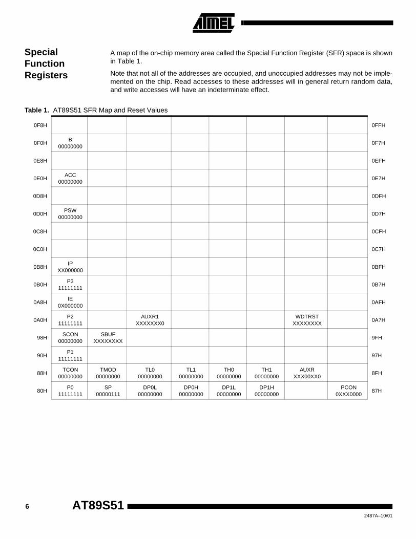
Special Function Registers
A map of the on-chip memory area called the Special Function Register (SFR) space is shownin Table 1.
Note that not all of the addresses are occupied, and unoccupied addresses may not be imple-mented on the chip. Read accesses to these addresses will in general return random data,and write accesses will have an indeterminate effect.
Table 1. AT89S51 SFR Map and Reset Values
0F8H 0FFH
0F0HB
000000000F7H
0E8H 0EFH
0E0HACC
000000000E7H
0D8H 0DFH
0D0HPSW
000000000D7H
0C8H 0CFH
0C0H 0C7H
0B8HIP
XX0000000BFH
0B0HP3
111111110B7H
0A8HIE
0X0000000AFH
0A0HP2
11111111AUXR1
XXXXXXX0WDTRST
XXXXXXXX0A7H
98HSCON
00000000SBUF
XXXXXXXX9FH
90HP1
1111111197H
88HTCON
00000000TMOD
00000000TL0
00000000TL1
00000000TH0
00000000TH1
00000000AUXR
XXX00XX08FH
80HP0
11111111SP
00000111DP0L
00000000DP0H
00000000DP1L
00000000DP1H
00000000PCON
0XXX000087H
6 AT89S512487A–10/01

AT89S51
User software should not write 1s to these unlisted locations, since they may be used in futureproducts to invoke new features. In that case, the reset or inactive values of the new bits willalways be 0.
Interrupt Registers: The individual interrupt enable bits are in the IE register. Two prioritiescan be set for each of the five interrupt sources in the IP register.
Dual Data Pointer Registers: To facilitate accessing both internal and external data memory,two banks of 16-bit Data Pointer Registers are provided: DP0 at SFR address locations 82H-83H and DP1 at 84H-85H. Bit DPS = 0 in SFR AUXR1 selects DP0 and DPS = 1 selects DP1.The user should always initialize the DPS bit to the appropriate value before accessing therespective Data Pointer Register.
Table 2. AUXR: Auxiliary Register
AUXR Address = 8EH Reset Value = XXX00XX0B
Not Bit Addressable
– – – WDIDLE DISRTO – – DISALE
Bit 7 6 5 4 3 2 1 0
– Reserved for future expansion
DISALE Disable/Enable ALE
DISALEOperating Mode
0 ALE is emitted at a constant rate of 1/6 the oscillator frequency
1 ALE is active only during a MOVX or MOVC instruction
DISRTO Disable/Enable Reset out
DISRTO
0 Reset pin is driven High after WDT times out
1 Reset pin is input only
WDIDLE Disable/Enable WDT in IDLE mode
WDIDLE
0 WDT continues to count in IDLE mode
1 WDT halts counting in IDLE mode
72487A–10/01

Power Off Flag: The Power Off Flag (POF) is located at bit 4 (PCON.4) in the PCON SFR.POF is set to “1” during power up. It can be set and rest under software control and is notaffected by reset.
Memory Organization
MCS-51 devices have a separate address space for Program and Data Memory. Up to 64Kbytes each of external Program and Data Memory can be addressed.
Program Memory If the EA pin is connected to GND, all program fetches are directed to external memory.
On the AT89S51, if EA is connected to VCC, program fetches to addresses 0000H throughFFFH are directed to internal memory and fetches to addresses 1000H through FFFFH aredirected to external memory.
Data Memory The AT89S51 implements 128 bytes of on-chip RAM. The 128 bytes are accessible via directand indirect addressing modes. Stack operations are examples of indirect addressing, so the128 bytes of data RAM are available as stack space.
Watchdog Timer (One-time Enabled with Reset-out)
The WDT is intended as a recovery method in situations where the CPU may be subjected tosoftware upsets. The WDT consists of a 14-bit counter and the Watchdog Timer Reset(WDTRST) SFR. The WDT is defaulted to disable from exiting reset. To enable the WDT, auser must write 01EH and 0E1H in sequence to the WDTRST register (SFR location 0A6H).When the WDT is enabled, it will increment every machine cycle while the oscillator is running.The WDT timeout period is dependent on the external clock frequency. There is no way to dis-able the WDT except through reset (either hardware reset or WDT overflow reset). WhenWDT overflows, it will drive an output RESET HIGH pulse at the RST pin.
Using the WDT To enable the WDT, a user must write 01EH and 0E1H in sequence to the WDTRST register(SFR location 0A6H). When the WDT is enabled, the user needs to service it by writing 01EHand 0E1H to WDTRST to avoid a WDT overflow. The 14-bit counter overflows when it reaches16383 (3FFFH), and this will reset the device. When the WDT is enabled, it will incrementevery machine cycle while the oscillator is running. This means the user must reset the WDTat least every 16383 machine cycles. To reset the WDT the user must write 01EH and 0E1Hto WDTRST. WDTRST is a write-only register. The WDT counter cannot be read or written.When WDT overflows, it will generate an output RESET pulse at the RST pin. The RESETpulse duration is 98xTOSC, where TOSC=1/FOSC. To make the best use of the WDT, it
Table 3. AUXR1: Auxiliary Register 1
AUXR1Address = A2H
Reset Value = XXXXXXX0B
Not Bit Addressable
– – – – – – – DPS
Bit 7 6 5 4 3 2 1 0
– Reserved for future expansion
DPS Data Pointer Register Select
DPS
0 Selects DPTR Registers DP0L, DP0H
1 Selects DPTR Registers DP1L, DP1H
8 AT89S512487A–10/01
AT89S51
should be serviced in those sections of code that will periodically be executed within the timerequired to prevent a WDT reset.
WDT During Power-down and Idle
In Power-down mode the oscillator stops, which means the WDT also stops. While in Power-down mode, the user does not need to service the WDT. There are two methods of exitingPower-down mode: by a hardware reset or via a level-activated external interrupt, which isenabled prior to entering Power-down mode. When Power-down is exited with hardware reset,servicing the WDT should occur as it normally does whenever the AT89S51 is reset. ExitingPower-down with an interrupt is significantly different. The interrupt is held low long enough forthe oscillator to stabilize. When the interrupt is brought high, the interrupt is serviced. To pre-vent the WDT from resetting the device while the interrupt pin is held low, the WDT is notstarted until the interrupt is pulled high. It is suggested that the WDT be reset during the inter-rupt service for the interrupt used to exit Power-down mode.
To ensure that the WDT does not overflow within a few states of exiting Power-down, it is bestto reset the WDT just before entering Power-down mode.
Before going into the IDLE mode, the WDIDLE bit in SFR AUXR is used to determine whetherthe WDT continues to count if enabled. The WDT keeps counting during IDLE (WDIDLE bit =0) as the default state. To prevent the WDT from resetting the AT89S51 while in IDLE mode,the user should always set up a timer that will periodically exit IDLE, service the WDT, andreenter IDLE mode.
With WDIDLE bit enabled, the WDT will stop to count in IDLE mode and resumes the countupon exit from IDLE.
UART The UART in the AT89S51 operates the same way as the UART in the AT89C51. For furtherinformation on the UART operation, refer to the ATMEL Web site (http://www.atmel.com).From the home page, select ‘Products’, then ‘8051-Architecture Flash Microcontroller’, then‘Product Overview’.
Timer 0 and 1 Timer 0 and Timer 1 in the AT89S51 operate the same way as Timer 0 and Timer 1 in theAT89C51. For further information on the timers’ operation, refer to the ATMEL Web site(http://www.atmel.com). From the home page, select ‘Products’, then ‘8051-Architecture FlashMicrocontroller’, then ‘Product Overview’.
Interrupts The AT89S51 has a total of five interrupt vectors: two external interrupts (INT0 and INT1), twotimer interrupts (Timers 0 and 1), and the serial port interrupt. These interrupts are all shown inFigure 1.
Each of these interrupt sources can be individually enabled or disabled by setting or clearing abit in Special Function Register IE. IE also contains a global disable bit, EA, which disables allinterrupts at once.
Note that Table 4 shows that bit position IE.6 is unimplemented. In the AT89S51, bit positionIE.5 is also unimplemented. User software should not write 1s to these bit positions, since theymay be used in future AT89 products.
The Timer 0 and Timer 1 flags, TF0 and TF1, are set at S5P2 of the cycle in which the timersoverflow. The values are then polled by the circuitry in the next cycle
92487A–10/01

.
Figure 1. Interrupt Sources
Table 4. Interrupt Enable (IE) Register
(MSB) (LSB)
EA – – ES ET1 EX1 ET0 EX0
Enable Bit = 1 enables the interrupt.
Enable Bit = 0 disables the interrupt.
Symbol Position Function
EA IE.7 Disables all interrupts. If EA = 0, no interrupt is acknowledged. If EA = 1, each interrupt source is individually enabled or disabled by setting or clearing its enable bit.
– IE.6 Reserved
– IE.5 Reserved
ES IE.4 Serial Port interrupt enable bit
ET1 IE.3 Timer 1 interrupt enable bit
EX1 IE.2 External interrupt 1 enable bit
ET0 IE.1 Timer 0 interrupt enable bit
EX0 IE.0 External interrupt 0 enable bit
User software should never write 1s to reserved bits, because they may be used in future AT89 products.
IE1
IE0
1
1
0
0
TF1
TF0
INT1
INT0
TIRI
10 AT89S512487A–10/01

AT89S51
11
Oscillator Characteristics
XTAL1 and XTAL2 are the input and output, respectively, of an inverting amplifier that can beconfigured for use as an on-chip oscillator, as shown in Figure 2. Either a quartz crystal orceramic resonator may be used. To drive the device from an external clock source, XTAL2should be left unconnected while XTAL1 is driven, as shown in Figure 3. There are no require-ments on the duty cycle of the external clock signal, since the input to the internal clockingcircuitry is through a divide-by-two flip-flop, but minimum and maximum voltage high and lowtime specifications must be observed.
Figure 2. Oscillator Connections
Note: C1, C2 = 30 pF ± 10 pF for Crystals = 40 pF ± 10 pF for Ceramic Resonators
Figure 3. External Clock Drive Configuration
Idle Mode In idle mode, the CPU puts itself to sleep while all the on-chip peripherals remain active. Themode is invoked by software. The content of the on-chip RAM and all the special functionregisters remain unchanged during this mode. The idle mode can be terminated by anyenabled interrupt or by a hardware reset.
Note that when idle mode is terminated by a hardware reset, the device normally resumes pro-gram execution from where it left off, up to two machine cycles before the internal resetalgorithm takes control. On-chip hardware inhibits access to internal RAM in this event, butaccess to the port pins is not inhibited. To eliminate the possibility of an unexpected write to aport pin when idle mode is terminated by a reset, the instruction following the one that invokesidle mode should not write to a port pin or to external memory.
Power-down Mode
In the Power-down mode, the oscillator is stopped, and the instruction that invokes Power-down is the last instruction executed. The on-chip RAM and Special Function Registers retaintheir values until the Power-down mode is terminated. Exit from Power-down mode can be ini-tiated either by a hardware reset or by activation of an enabled external interrupt into INT0 orINT1. Reset redefines the SFRs but does not change the on-chip RAM. The reset should notbe activated before VCC is restored to its normal operating level and must be held active longenough to allow the oscillator to restart and stabilize.
C2XTAL2
GND
XTAL1C1
XTAL2
XTAL1
GND
NC
EXTERNALOSCILLATOR
SIGNAL
2487A–10/01

Program Memory Lock Bits
The AT89S51 has three lock bits that can be left unprogrammed (U) or can be programmed(P) to obtain the additional features listed in the following table.
When lock bit 1 is programmed, the logic level at the EA pin is sampled and latched duringreset. If the device is powered up without a reset, the latch initializes to a random value andholds that value until reset is activated. The latched value of EA must agree with the currentlogic level at that pin in order for the device to function properly.
Programming the Flash – Parallel Mode
The AT89S51 is shipped with the on-chip Flash memory array ready to be programmed. Theprogramming interface needs a high-voltage (12-volt) program enable signal and is compati-ble with conventional third-party Flash or EPROM programmers.
The AT89S51 code memory array is programmed byte-by-byte.
Programming Algorithm: Before programming the AT89S51, the address, data, and controlsignals should be set up according to the Flash programming mode table and Figures 13 and14. To program the AT89S51, take the following steps:
1. Input the desired memory location on the address lines.
2. Input the appropriate data byte on the data lines.
3. Activate the correct combination of control signals.
4. Raise EA/VPP to 12V.
5. Pulse ALE/PROG once to program a byte in the Flash array or the lock bits. The byte-write cycle is self-timed and typically takes no more than 50 µs. Repeat steps 1 through 5, changing the address and data for the entire array or until the end of the object file is reached.
Data Polling: The AT89S51 features Data Polling to indicate the end of a byte write cycle.During a write cycle, an attempted read of the last byte written will result in the complement ofthe written data on P0.7. Once the write cycle has been completed, true data is valid on all out-puts, and the next cycle may begin. Data Polling may begin any time after a write cycle hasbeen initiated.
Table 5. Status of External Pins During Idle and Power-down Modes
Mode Program Memory ALE PSEN PORT0 PORT1 PORT2 PORT3
Idle Internal 1 1 Data Data Data Data
Idle External 1 1 Float Data Address Data
Power-down Internal 0 0 Data Data Data Data
Power-down External 0 0 Float Data Data Data
Table 6. Lock Bit Protection Modes
Program Lock Bits
LB1 LB2 LB3 Protection Type
1 U U U No program lock features
2 P U U MOVC instructions executed from external program memory are disabled from fetching code bytes from internal memory, EA is sampled and latched on reset, and further programming of the Flash memory is disabled
3 P P U Same as mode 2, but verify is also disabled
4 P P P Same as mode 3, but external execution is also disabled
12 AT89S512487A–10/01

AT89S51
Ready/Busy: The progress of byte programming can also be monitored by the RDY/BSY out-put signal. P3.0 is pulled low after ALE goes high during programming to indicate BUSY. P3.0is pulled high again when programming is done to indicate READY.
Program Verify: If lock bits LB1 and LB2 have not been programmed, the programmed codedata can be read back via the address and data lines for verification. The status of the individ-ual lock bits can be verified directly by reading them back.
Reading the Signature Bytes: The signature bytes are read by the same procedure as a nor-mal verification of locations 000H, 100H, and 200H, except that P3.6 and P3.7 must be pulledto a logic low. The values returned are as follows.
(000H) = 1EH indicates manufactured by Atmel(100H) = 51H indicates 89S51(200H) = 06H
Chip Erase: In the parallel programming mode, a chip erase operation is initiated by using theproper combination of control signals and by pulsing ALE/PROG low for a duration of 200 ns -500 ns.
In the serial programming mode, a chip erase operation is initiated by issuing the Chip Eraseinstruction. In this mode, chip erase is self-timed and takes about 500 ms.
During chip erase, a serial read from any address location will return 00H at the data output.
Programming the Flash – Serial Mode
The Code memory array can be programmed using the serial ISP interface while RST ispulled to VCC. The serial interface consists of pins SCK, MOSI (input) and MISO (output). AfterRST is set high, the Programming Enable instruction needs to be executed first before otheroperations can be executed. Before a reprogramming sequence can occur, a Chip Eraseoperation is required.
The Chip Erase operation turns the content of every memory location in the Code array intoFFH.
Either an external system clock can be supplied at pin XTAL1 or a crystal needs to be con-nected across pins XTAL1 and XTAL2. The maximum serial clock (SCK) frequency should beless than 1/16 of the crystal frequency. With a 33 MHz oscillator clock, the maximum SCK fre-quency is 2 MHz.
Serial Programming Algorithm
To program and verify the AT89S51 in the serial programming mode, the following sequenceis recommended:
1. Power-up sequence:
Apply power between VCC and GND pins.
Set RST pin to “H”.
If a crystal is not connected across pins XTAL1 and XTAL2, apply a 3 MHz to 33 MHzclock to XTAL1 pin and wait for at least 10 milliseconds.
2. Enable serial programming by sending the Programming Enable serial instruction to pin MOSI/P1.5. The frequency of the shift clock supplied at pin SCK/P1.7 needs to be less than the CPU clock at XTAL1 divided by 16.
3. The Code array is programmed one byte at a time in either the Byte or Page mode. The write cycle is self-timed and typically takes less than 0.5 ms at 5V.
4. Any memory location can be verified by using the Read instruction that returns the con-tent at the selected address at serial output MISO/P1.6.
5. At the end of a programming session, RST can be set low to commence normal device operation.
132487A–10/01
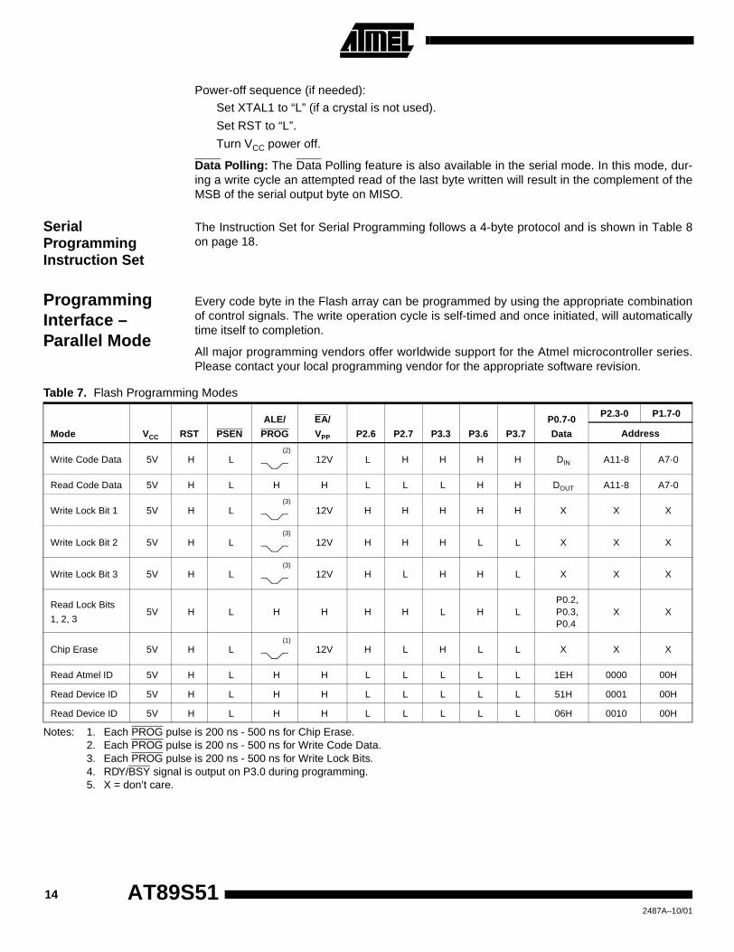
Power-off sequence (if needed):
Set XTAL1 to “L” (if a crystal is not used).
Set RST to “L”.
Turn VCC power off.
Data Polling: The Data Polling feature is also available in the serial mode. In this mode, dur-ing a write cycle an attempted read of the last byte written will result in the complement of theMSB of the serial output byte on MISO.
Serial Programming Instruction Set
The Instruction Set for Serial Programming follows a 4-byte protocol and is shown in Table 8on page 18.
Programming Interface – Parallel Mode
Every code byte in the Flash array can be programmed by using the appropriate combinationof control signals. The write operation cycle is self-timed and once initiated, will automaticallytime itself to completion.
All major programming vendors offer worldwide support for the Atmel microcontroller series.Please contact your local programming vendor for the appropriate software revision.
Notes: 1. Each PROG pulse is 200 ns - 500 ns for Chip Erase.2. Each PROG pulse is 200 ns - 500 ns for Write Code Data.3. Each PROG pulse is 200 ns - 500 ns for Write Lock Bits.4. RDY/BSY signal is output on P3.0 during programming.5. X = don’t care.
Table 7. Flash Programming Modes
Mode VCC RST PSEN
ALE/
PROG
EA/
VPP P2.6 P2.7 P3.3 P3.6 P3.7
P0.7-0
Data
P2.3-0 P1.7-0
Address
Write Code Data 5V H L(2)
12V L H H H H DIN A11-8 A7-0
Read Code Data 5V H L H H L L L H H DOUT A11-8 A7-0
Write Lock Bit 1 5V H L(3)
12V H H H H H X X X
Write Lock Bit 2 5V H L(3)
12V H H H L L X X X
Write Lock Bit 3 5V H L(3)
12V H L H H L X X X
Read Lock Bits
1, 2, 35V H L H H H H L H L
P0.2,P0.3,P0.4
X X
Chip Erase 5V H L(1)
12V H L H L L X X X
Read Atmel ID 5V H L H H L L L L L 1EH 0000 00H
Read Device ID 5V H L H H L L L L L 51H 0001 00H
Read Device ID 5V H L H H L L L L L 06H 0010 00H
14 AT89S512487A–10/01

AT89S51
Figure 4. Programming the Flash Memory (Parallel Mode)
Figure 5. Verifying the Flash Memory (Parallel Mode)
P1.0-P1.7
P2.6
P3.6
P2.0 - P2.3
A0 - A7ADDR.
0000H/FFFH
SEE FLASHPROGRAMMINGMODES TABLE
3-33 MHz
P0
V
P2.7
PGMDATA
PROG
V /VIH PP
VIH
ALE
P3.7
XTAL2 EA
RST
PSEN
XTAL1
GND
VCC
AT89S51
P3.3
P3.0RDY/BSY
A8 - A11
CC
P1.0-P1.7
P2.6
P3.6
P2.0 - P2.3
A0 - A7ADDR.
0000H/FFFH
SEE FLASHPROGRAMMINGMODES TABLE
3-33 MHz
P0
P2.7
PGM DATA(USE 10KPULLUPS)
VIH
VIH
ALE
P3.7
XTAL2 EA
RST
PSEN
XTAL1
GND
VCC
AT89S51
P3.3
A8 - A11
VCC
152487A–10/01

Figure 6. Flash Programming and Verification Waveforms – Parallel Mode
Flash Programming and Verification Characteristics (Parallel Mode)TA = 20°C to 30°C, VCC = 4.5 to 5.5V
Symbol Parameter Min Max Units
VPP Programming Supply Voltage 11.5 12.5 V
IPP Programming Supply Current 10 mA
ICC VCC Supply Current 30 mA
1/tCLCL Oscillator Frequency 3 33 MHz
tAVGL Address Setup to PROG Low 48tCLCL
tGHAX Address Hold After PROG 48tCLCL
tDVGL Data Setup to PROG Low 48tCLCL
tGHDX Data Hold After PROG 48tCLCL
tEHSH P2.7 (ENABLE) High to VPP 48tCLCL
tSHGL VPP Setup to PROG Low 10 µs
tGHSL VPP Hold After PROG 10 µs
tGLGH PROG Width 0.2 1 µs
tAVQV Address to Data Valid 48tCLCL
tELQV ENABLE Low to Data Valid 48tCLCL
tEHQZ Data Float After ENABLE 0 48tCLCL
tGHBL PROG High to BUSY Low 1.0 µs
tWC Byte Write Cycle Time 50 µs
tGLGHtGHSL
tAVGL
tSHGL
tDVGLtGHAX
tAVQV
tGHDX
tEHSH tELQV
tWC
BUSY READY
tGHBL
tEHQZ
P1.0 - P1.7P2.0 - P2.3
ALE/PROG
PORT 0
LOGIC 1LOGIC 0EA/VPP
VPP
P2.7(ENABLE)
P3.0(RDY/BSY)
PROGRAMMINGADDRESS
VERIFICATIONADDRESS
DATA IN DATA OUT
16 AT89S512487A–10/01

AT89S51
Figure 7. Flash Memory Serial Downloading
Flash Programming and Verification Waveforms – Serial Mode
Figure 8. Serial Programming Waveforms
P1.7/SCK
DATA OUTPUT
INSTRUCTIONINPUT
CLOCK IN
3-33 MHz
P1.5/MOSI
VIH
XTAL2
RSTXTAL1
GND
VCC
AT89S51
P1.6/MISO
VCC
7 6 5 4 3 2 1 0
172487A–10/01

Notes: 1. The signature bytes are not readable in Lock Bit Modes 3 and 4.2. B1 = 0, B2 = 0 → Mode 1, no lock protection
B1 = 0, B2 = 1 → Mode 2, lock bit 1 activatedB1 = 1, B2 = 0 → Mode 3, lock bit 2 activatedB1 = 1, B1 = 1 → Mode 4, lock bit 3 activated
After Reset signal is high, SCK should be low for at least 64 system clocks before it goes high to clock in the enable databytes. No pulsing of Reset signal is necessary. SCK should be no faster than 1/16 of the system clock at XTAL1.
For Page Read/Write, the data always starts from byte 0 to 255. After the command byte and upper address byte arelatched, each byte thereafter is treated as data until all 256 bytes are shifted in/out. Then the next instruction will be ready tobe decoded.
Table 8. Serial Programming Instruction Set
Instruction
Instruction Format
OperationByte 1 Byte 2 Byte 3 Byte 4
Programming Enable 1010 1100 0101 0011 xxxx xxxx xxxx xxxx0110 1001 (Output)
Enable Serial Programming while RST is high
Chip Erase 1010 1100 100x xxxx xxxx xxxx xxxx xxxx Chip Erase Flash memory array
Read Program Memory(Byte Mode)
0010 0000 xxxx Read data from Program memory in the byte mode
Write Program Memory(Byte Mode)
0100 0000 xxxx Write data to Program memory in the byte mode
Write Lock Bits(2) 1010 1100 1110 00 xxxx xxxx xxxx xxxx Write Lock bits. See Note (2).
Read Lock Bits 0010 0100 xxxx xxxx xxxx xxxx xx xx Read back current status of the lock bits (a programmed lock bit reads back as a “1”)
Read Signature Bytes(1) 0010 1000 xxx xxx xxxx Signature Byte Read Signature Byte
Read Program Memory(Page Mode)
0011 0000 xxxx Byte 0 Byte 1... Byte 255
Read data from Program memory in the Page Mode (256 bytes)
Write Program Memory(Page Mode)
0101 0000 xxxx Byte 0 Byte 1... Byte 255
Write data to Program memory in the Page Mode (256 bytes)
Each of the lock bits needs to be activated sequentially before Mode 4 can be executed.
D7
D6
D5
D4
D3
D2
D1
D0
A7
A6
A5
A4
A3
A2 A1
A0
A11
A10 A
9A
8B
2B
1
A11
A10 A
9A
8
A7
A6
A5
A4
A3
A2 A1
A0
D7
D6
D5
D4
D3
D2
D1
D0
LB3
LB2
LB1
A5
A4
A3
A2
A1
A11
A10 A
9A
8
A11
A10 A
9A
8
A0
18 AT89S512487A–10/01

AT89S51
192487A–10/01
Serial Programming Characteristics
Figure 9. Serial Programming Timing
MOSI
MISO
SCK
tOVSH
tSHSL
tSLSHtSHOX
tSLIV
Table 9. Serial Programming Characteristics, TA = -40° C to 85° C, VCC = 4.0 - 5.5V (Unless Otherwise Noted)
Symbol Parameter Min Typ Max Units
1/tCLCL Oscillator Frequency 0 33 MHz
tCLCL Oscillator Period 30 ns
tSHSL SCK Pulse Width High 8 tCLCL ns
tSLSH SCK Pulse Width Low 8 tCLCL ns
tOVSH MOSI Setup to SCK High tCLCL ns
tSHOX MOSI Hold after SCK High 2 tCLCL ns
tSLIV SCK Low to MISO Valid 10 16 32 ns
tERASE Chip Erase Instruction Cycle Time 500 ms
tSWC Serial Byte Write Cycle Time 64 tCLCL + 400 µs

Notes: 1. Under steady state (non-transient) conditions, IOL must be externally limited as follows:Maximum IOL per port pin: 10 mAMaximum IOL per 8-bit port:Port 0: 26 mA Ports 1, 2, 3: 15 mAMaximum total IOL for all output pins: 71 mAIf IOL exceeds the test condition, VOL may exceed the related specification. Pins are not guaranteed to sink current greaterthan the listed test conditions.
2. Minimum VCC for Power-down is 2V.
Absolute Maximum Ratings*Operating Temperature.................................. -55°C to +125°C *NOTICE: Stresses beyond those listed under “Absolute
Maximum Ratings” may cause permanent dam-age to the device. This is a stress rating only and functional operation of the device at these or any other conditions beyond those indicated in the operational sections of this specification is not implied. Exposure to absolute maximum rating conditions for extended periods may affect device reliability.
Storage Temperature ..................................... -65°C to +150°C
Voltage on Any Pinwith Respect to Ground .....................................-1.0V to +7.0V
Maximum Operating Voltage ............................................ 6.6V
DC Output Current...................................................... 15.0 mA
DC CharacteristicsThe values shown in this table are valid for TA = -40°C to 85°C and VCC = 4.0V to 5.5V, unless otherwise noted.
Symbol Parameter Condition Min Max Units
VIL Input Low Voltage (Except EA) -0.5 0.2 VCC-0.1 V
VIL1 Input Low Voltage (EA) -0.5 0.2 VCC-0.3 V
VIH Input High Voltage (Except XTAL1, RST) 0.2 VCC+0.9 VCC+0.5 V
VIH1 Input High Voltage (XTAL1, RST) 0.7 VCC VCC+0.5 V
VOL
Output Low Voltage(1) (Ports 1,2,3) IOL = 1.6 mA
0.45 V
VOL1
Output Low Voltage(1)
(Port 0, ALE, PSEN) IOL = 3.2 mA0.45 V
VOH
Output High Voltage(Ports 1,2,3, ALE, PSEN)
IOH = -60 µA, VCC = 5V ± 10% 2.4 V
IOH = -25 µA 0.75 VCC V
IOH = -10 µA 0.9 VCC V
VOH1
Output High Voltage(Port 0 in External Bus Mode)
IOH = -800 µA, VCC = 5V ± 10% 2.4 V
IOH = -300 µA 0.75 VCC V
IOH = -80 µA 0.9 VCC V
IIL
Logical 0 Input Current (Ports 1,2,3) VIN = 0.45V
-50 µA
ITL
Logical 1 to 0 Transition Current (Ports 1,2,3) VIN = 2V, VCC = 5V ± 10%
-650 µA
ILI
Input Leakage Current (Port 0, EA) 0.45 < VIN < VCC
±10 µA
RRST Reset Pulldown Resistor 50 300 KΩ
CIO Pin Capacitance Test Freq. = 1 MHz, TA = 25°C 10 pF
ICC
Power Supply Current
Active Mode, 12 MHz 25 mA
Idle Mode, 12 MHz 6.5 mA
Power-down Mode(2) VCC = 5.5V 50 µA
20 AT89S512487A–10/01

AT89S51
AC Characteristics Under operating conditions, load capacitance for Port 0, ALE/PROG, and PSEN = 100 pF; load capacitance for all otheroutputs = 80 pF.
External Program and Data Memory Characteristics
Symbol Parameter
12 MHz Oscillator Variable Oscillator
UnitsMin Max Min Max
1/tCLCL Oscillator Frequency 0 33 MHz
tLHLL ALE Pulse Width 127 2tCLCL-40 ns
tAVLL Address Valid to ALE Low 43 tCLCL-25 ns
tLLAX Address Hold After ALE Low 48 tCLCL-25 ns
tLLIV ALE Low to Valid Instruction In 233 4tCLCL-65 ns
tLLPL ALE Low to PSEN Low 43 tCLCL-25 ns
tPLPH PSEN Pulse Width 205 3tCLCL-45 ns
tPLIV PSEN Low to Valid Instruction In 145 3tCLCL-60 ns
tPXIX Input Instruction Hold After PSEN 0 0 ns
tPXIZ Input Instruction Float After PSEN 59 tCLCL-25 ns
tPXAV PSEN to Address Valid 75 tCLCL-8 ns
tAVIV Address to Valid Instruction In 312 5tCLCL-80 ns
tPLAZ PSEN Low to Address Float 10 10 ns
tRLRH RD Pulse Width 400 6tCLCL-100 ns
tWLWH WR Pulse Width 400 6tCLCL-100 ns
tRLDV RD Low to Valid Data In 252 5tCLCL-90 ns
tRHDX Data Hold After RD 0 0 ns
tRHDZ Data Float After RD 97 2tCLCL-28 ns
tLLDV ALE Low to Valid Data In 517 8tCLCL-150 ns
tAVDV Address to Valid Data In 585 9tCLCL-165 ns
tLLWL ALE Low to RD or WR Low 200 300 3tCLCL-50 3tCLCL+50 ns
tAVWL Address to RD or WR Low 203 4tCLCL-75 ns
tQVWX Data Valid to WR Transition 23 tCLCL-30 ns
tQVWH Data Valid to WR High 433 7tCLCL-130 ns
tWHQX Data Hold After WR 33 tCLCL-25 ns
tRLAZ RD Low to Address Float 0 0 ns
tWHLH RD or WR High to ALE High 43 123 tCLCL-25 tCLCL+25 ns
212487A–10/01

External Program Memory Read Cycle
External Data Memory Read Cycle
tLHLL
tLLIV
tPLIV
tLLAXtPXIZ
tPLPH
tPLAZtPXAV
tAVLL tLLPL
tAVIV
tPXIX
ALE
PSEN
PORT 0
PORT 2 A8 - A15
A0 - A7 A0 - A7
A8 - A15
INSTR IN
tLHLL
tLLDV
tLLWL
tLLAX
tWHLH
tAVLL
tRLRH
tAVDV
tAVWL
tRLAZ tRHDX
tRLDV tRHDZ
A0 - A7 FROM RI OR DPL
ALE
PSEN
RD
PORT 0
PORT 2 P2.0 - P2.7 OR A8 - A15 FROM DPH
A0 - A7 FROM PCL
A8 - A15 FROM PCH
DATA IN INSTR IN
22 AT89S512487A–10/01

AT89S51
External Data Memory Write Cycle
External Clock Drive Waveforms
tLHLL
tLLWL
tLLAX
tWHLH
tAVLL
tWLWH
tAVWL
tQVWXtQVWH
tWHQX
A0 - A7 FROM RI OR DPL
ALE
PSEN
WR
PORT 0
PORT 2 P2.0 - P2.7 OR A8 - A15 FROM DPH
A0 - A7 FROM PCL
A8 - A15 FROM PCH
DATA OUT INSTR IN
tCHCX
tCHCX
tCLCX
tCLCL
tCHCLtCLCHV - 0.5VCC
0.45V0.2 V - 0.1VCC
0.7 VCC
External Clock DriveSymbol Parameter Min Max Units
1/tCLCL Oscillator Frequency 0 33 MHz
tCLCL Clock Period 30 ns
tCHCX High Time 12 ns
tCLCX Low Time 12 ns
tCLCH Rise Time 5 ns
tCHCL Fall Time 5 ns
232487A–10/01

Shift Register Mode Timing Waveforms
AC Testing Input/Output Waveforms(1)
Note: 1. AC Inputs during testing are driven at VCC - 0.5V for a logic 1 and 0.45V for a logic 0. Timing measurements are made at VIHmin. for a logic 1 and VIL max. for a logic 0.
Float Waveforms(1)
Note: 1. For timing purposes, a port pin is no longer floating when a 100 mV change from load voltage occurs. A port pin begins tofloat when a 100 mV change from the loaded VOH/VOL level occurs.
Serial Port Timing: Shift Register Mode Test ConditionsThe values in this table are valid for VCC = 4.0V to 5.5V and Load Capacitance = 80 pF.
Symbol Parameter
12 MHz Osc Variable Oscillator
UnitsMin Max Min Max
tXLXL Serial Port Clock Cycle Time 1.0 12tCLCL µs
tQVXH Output Data Setup to Clock Rising Edge 700 10tCLCL-133 ns
tXHQX Output Data Hold After Clock Rising Edge 50 2tCLCL-80 ns
tXHDX Input Data Hold After Clock Rising Edge 0 0 ns
tXHDV Clock Rising Edge to Input Data Valid 700 10tCLCL-133 ns
tXHDV
tQVXH
tXLXL
tXHDX
tXHQX
ALE
INPUT DATA
CLEAR RI
OUTPUT DATA
WRITE TO SBUF
INSTRUCTION
CLOCK
0
0
1
1
2
2
3
3
4
4
5
5
6
6
7
7
SET TI
SET RI
8
VALID VALIDVALID VALIDVALID VALIDVALID VALID
0.45V
TEST POINTS
V - 0.5VCC 0.2 V + 0.9VCC
0.2 V - 0.1VCC
VLOAD+ 0.1V
Timing ReferencePoints
V
LOAD- 0.1V
LOAD
V VOL+ 0.1V
VOL- 0.1V
24 AT89S512487A–10/01

AT89S51
Ordering InformationSpeed(MHz)
PowerSupply Ordering Code Package Operation Range
24 4.0V to 5.5V AT89S51-24ACAT89S51-24JC
AT89S51-24PC
44A44J
40P6
Commercial(0° C to 70° C)
AT89S51-24AIAT89S51-24JIAT89S51-24PI
44A44J40P6
Industrial(-40° C to 85° C)
33 4.5V to 5.5V AT89S51-33AC
AT89S51-33JCAT89S51-33PC
44A
44J40P6
Commercial
(0° C to 70° C)
= Preliminary Availability
Package Type
44A 44-lead, Thin Plastic Gull Wing Quad Flatpack (TQFP)
44J 44-lead, Plastic J-leaded Chip Carrier (PLCC)
40P6 40-pin, 0.600" Wide, Plastic Dual Inline Package (PDIP)
252487A–10/01

Packaging Information
*Controlling dimension: millimeters
1.20(0.047) MAX
10.10(0.394)9.90(0.386)
SQ
12.21(0.478)11.75(0.458)
SQ
0.75(0.030)0.45(0.018)
0.15(0.006)0.05(0.002)
0.20(.008)0.09(.003)
07
0.80(0.031) BSC
PIN 1 ID
0.45(0.018)0.30(0.012)
26 AT89S51
.045(1.14) X 45° PIN NO. 1IDENTIFY
.045(1.14) X 30° - 45° .012(.305).008(.203)
.021(.533)
.013(.330)
.630(16.0)
.590(15.0)
.043(1.09)
.020(.508)
.120(3.05)
.090(2.29).180(4.57).165(4.19)
.500(12.7) REF SQ
.032(.813)
.026(.660)
.050(1.27) TYP
.022(.559) X 45° MAX (3X)
.656(16.7)
.650(16.5)
.695(17.7)
.685(17.4)SQ
SQ
2.07(52.6)2.04(51.8) PIN
1
.566(14.4)
.530(13.5)
.090(2.29)MAX
.005(.127)MIN
.065(1.65)
.015(.381)
.022(.559)
.014(.356).065(1.65).041(1.04)
015
REF
.690(17.5)
.610(15.5)
.630(16.0)
.590(15.0)
.012(.305)
.008(.203)
.110(2.79)
.090(2.29)
.161(4.09)
.125(3.18)
SEATINGPLANE
.220(5.59)MAX
1.900(48.26) REF
JEDEC STANDARD MS-011 AC
44A, 44-lead, Thin (1.0 mm) Plastic Gull Wing Quad Flat Package (TQFP)Dimensions in Millimeters and (Inches)*
44J, 44-lead, Plastic J-leaded Chip Carrier (PLCC)Dimensions in Inches and (Millimeters)
40P6, 40-pin, 0.600" Wide, Plastic Dual Inline Package (PDIP)Dimensions in Inches and (Millimeters)
2487A–10/01

© Atmel Corporation 2001.Atmel Corporation makes no warranty for the use of its products, other than those expressly contained in the Company’s standard warrantywhich is detailed in Atmel’s Terms and Conditions located on the Company’s web site. The Company assumes no responsibility for any errorswhich may appear in this document, reserves the right to change devices or specifications detailed herein at any time without notice, and doesnot make any commitment to update the information contained herein. No licenses to patents or other intellectual property of Atmel are grantedby the Company in connection with the sale of Atmel products, expressly or by implication. Atmel’s products are not authorized for use as criticalcomponents in life support devices or systems.
Atmel Headquarters Atmel Product Operations
Corporate Headquarters2325 Orchard ParkwaySan Jose, CA 95131TEL (408) 441-0311FAX (408) 487-2600
EuropeAtmel SarLRoute des Arsenaux 41Casa Postale 80CH-1705 FribourgSwitzerlandTEL (41) 26-426-5555FAX (41) 26-426-5500
AsiaAtmel Asia, Ltd.Room 1219Chinachem Golden Plaza77 Mody Road TsimhatsuiEast KowloonHong KongTEL (852) 2721-9778FAX (852) 2722-1369
JapanAtmel Japan K.K.9F, Tonetsu Shinkawa Bldg.1-24-8 ShinkawaChuo-ku, Tokyo 104-0033JapanTEL (81) 3-3523-3551FAX (81) 3-3523-7581
Atmel Colorado Springs1150 E. Cheyenne Mtn. Blvd.Colorado Springs, CO 80906TEL (719) 576-3300FAX (719) 540-1759
Atmel GrenobleAvenue de RochepleineBP 12338521 Saint-Egreve Cedex, FranceTEL (33) 4-7658-3000FAX (33) 4-7658-3480
Atmel HeilbronnTheresienstrasse 2POB 3535D-74025 Heilbronn, GermanyTEL (49) 71 31 67 25 94FAX (49) 71 31 67 24 23
Atmel NantesLa ChantrerieBP 7060244306 Nantes Cedex 3, FranceTEL (33) 0 2 40 18 18 18FAX (33) 0 2 40 18 19 60
Atmel RoussetZone Industrielle13106 Rousset Cedex, FranceTEL (33) 4-4253-6000FAX (33) 4-4253-6001
Atmel Smart Card ICsScottish Enterprise Technology ParkEast Kilbride, Scotland G75 0QRTEL (44) 1355-357-000FAX (44) 1355-242-743
Web Sitehttp://www.atmel.com
Printed on recycled paper.
ATMEL® is the registered trademark of Atmel.
MCS-51® is the registered trademark of Intel Corporation. Terms and product names in this document may betrademarks of others.
2487A–10/01/xM

L293, L293DQUADRUPLE HALF-H DRIVERS
SLRS008B – SEPTEMBER 1986 – REVISED JUNE 2002
1POST OFFICE BOX 655303 • DALLAS, TEXAS 75265
Featuring Unitrode L293 and L293DProducts Now From Texas Instruments
Wide Supply-Voltage Range: 4.5 V to 36 V
Separate Input-Logic Supply
Internal ESD Protection
Thermal Shutdown
High-Noise-Immunity Inputs
Functional Replacements for SGS L293 andSGS L293D
Output Current 1 A Per Channel(600 mA for L293D)
Peak Output Current 2 A Per Channel(1.2 A for L293D)
Output Clamp Diodes for InductiveTransient Suppression (L293D)
description
The L293 and L293D are quadruple high-currenthalf-H drivers. The L293 is designed to providebidirectional drive currents of up to 1 A at voltagesfrom 4.5 V to 36 V. The L293D is designed toprovide bidirectional drive currents of up to600-mA at voltages from 4.5 V to 36 V. Bothdevices are designed to drive inductive loads suchas relays, solenoids, dc and bipolar steppingmotors, as well as other high-current/high-voltageloads in positive-supply applications.
All inputs are TTL compatible. Each output is a complete totem-pole drive circuit, with a Darlington transistorsink and a pseudo-Darlington source. Drivers are enabled in pairs, with drivers 1 and 2 enabled by 1,2EN anddrivers 3 and 4 enabled by 3,4EN. When an enable input is high, the associated drivers are enabled and theiroutputs are active and in phase with their inputs. When the enable input is low, those drivers are disabled andtheir outputs are off and in the high-impedance state. With the proper data inputs, each pair of drivers formsa full-H (or bridge) reversible drive suitable for solenoid or motor applications.
On the L293, external high-speed output clamp diodes should be used for inductive transient suppression.
A VCC1 terminal, separate from VCC2, is provided for the logic inputs to minimize device power dissipation.
The L293and L293D are characterized for operation from 0°C to 70°C.
Copyright 2002, Texas Instruments IncorporatedPRODUCTION DATA information is current as of publication date.Products conform to specifications per the terms of Texas Instrumentsstandard warranty. Production processing does not necessarily includetesting of all parameters.
Please be aware that an important notice concerning availability, standard warranty, and use in critical applications ofTexas Instruments semiconductor products and disclaimers thereto appears at the end of this data sheet.
HEAT SINK ANDGROUND
HEAT SINK ANDGROUND
1
2
3
4
5
6
7
8
16
15
14
13
12
11
10
9
1,2EN1A1Y
2Y2A
VCC2
VCC14A4Y
3Y3A3,4EN
N, NE PACKAGE(TOP VIEW)
1
2
3
4
5
6
7
8
9
10
11
12
13
14
28
27
26
25
24
23
22
21
20
19
18
17
16
15
1,2EN1A1YNCNCNC
NCNC2Y2A
VCC2
VCC14A4YNCNCNC
NCNC3Y3A3,4EN
DWP PACKAGE(TOP VIEW)
HEAT SINK ANDGROUND
HEAT SINK ANDGROUND

L293, L293DQUADRUPLE HALF-H DRIVERS
SLRS008B – SEPTEMBER 1986 – REVISED JUNE 2002
2 POST OFFICE BOX 655303 • DALLAS, TEXAS 75265
block diagram
10
3
4
5
6
7
8 9
10
11
12
13
14
15
161
210
1
10
2
4
3
M
M
M
10
10
10
VC
VCC1
NOTE: Output diodes are internal in L293D.
TEXAS INSTRUMENTSAVAILABLE OPTIONS
PACKAGE
TAPLASTIC
DIP(NE)
0°C to 70°CL293NEL293DNE
AVAILABLE OPTIONS
PACKAGED DEVICES
TASMALL
OUTLINE(DWP)
PLASTICDIP(N)
0°C to 70°CL293DWPL293DDWP
L293NL293DN
The DWP package is available taped and reeled. Addthe suffix TR to device type (e.g., L293DWPTR).

L293, L293DQUADRUPLE HALF-H DRIVERS
SLRS008B – SEPTEMBER 1986 – REVISED JUNE 2002
3POST OFFICE BOX 655303 • DALLAS, TEXAS 75265
FUNCTION TABLE(each driver)
INPUTS† OUTPUTA EN Y
H H H
L H L
X L Z
H = high level, L = low level, X = irrelevant,Z = high impedance (off)† In the thermal shutdown mode, the output is
in the high-impedance state, regardless ofthe input levels.
logic diagram
ÁÁÁÁÁÁÁÁÁÁ
ÁÁÁÁÁÁ
ÁÁÁÁ
2
1
7
10
9
15
3
6
11
14
1A
1,2EN
2A
3A
3,4EN
4A
1Y
2Y
3Y
4Y
schematics of inputs and outputs (L293)
Input
VCC2
Output
GND
TYPICAL OF ALL OUTPUTSEQUIVALENT OF EACH INPUT
VCC1
CurrentSource
GND

L293, L293DQUADRUPLE HALF-H DRIVERS
SLRS008B – SEPTEMBER 1986 – REVISED JUNE 2002
4 POST OFFICE BOX 655303 • DALLAS, TEXAS 75265
schematics of inputs and outputs (L293D)
Input
VCC2
Output
GND
TYPICAL OF ALL OUTPUTSEQUIVALENT OF EACH INPUT
VCC1
CurrentSource
GND
absolute maximum ratings over operating free-air temperature range (unless otherwise noted)†
Supply voltage, VCC1 (see Note 1) 36 V. . . . . . . . . . . . . . . . . . . . . . . . . . . . . . . . . . . . . . . . . . . . . . . . . . . . . . . . . . . Output supply voltage, VCC2 36 V. . . . . . . . . . . . . . . . . . . . . . . . . . . . . . . . . . . . . . . . . . . . . . . . . . . . . . . . . . . . . . . . Input voltage, VI 7 V. . . . . . . . . . . . . . . . . . . . . . . . . . . . . . . . . . . . . . . . . . . . . . . . . . . . . . . . . . . . . . . . . . . . . . . . . . . . Output voltage range, VO –3 V to VCC2 + 3 V. . . . . . . . . . . . . . . . . . . . . . . . . . . . . . . . . . . . . . . . . . . . . . . . . . . . . . Peak output current, IO (nonrepetitive, t ≤ 5 ms): L293 ±2 A. . . . . . . . . . . . . . . . . . . . . . . . . . . . . . . . . . . . . . . . . . Peak output current, IO (nonrepetitive, t ≤ 100 µs): L293D ±1.2 A. . . . . . . . . . . . . . . . . . . . . . . . . . . . . . . . . . . . Continuous output current, IO: L293 ±1 A. . . . . . . . . . . . . . . . . . . . . . . . . . . . . . . . . . . . . . . . . . . . . . . . . . . . . . . . . Continuous output current, IO: L293D ±600 mA. . . . . . . . . . . . . . . . . . . . . . . . . . . . . . . . . . . . . . . . . . . . . . . . . . . . Continuous total dissipation at (or below) 25°C free-air temperature (see Notes 2 and 3) 2075 mW. . . . . . . Continuous total dissipation at 80°C case temperature (see Note 3) 5000 mW. . . . . . . . . . . . . . . . . . . . . . . . . Maximum junction temperature, TJ 150°C. . . . . . . . . . . . . . . . . . . . . . . . . . . . . . . . . . . . . . . . . . . . . . . . . . . . . . . . . Lead temperature 1,6 mm (1/16 inch) from case for 10 seconds 260°C. . . . . . . . . . . . . . . . . . . . . . . . . . . . . . . Storage temperature range, Tstg –65°C to 150°C. . . . . . . . . . . . . . . . . . . . . . . . . . . . . . . . . . . . . . . . . . . . . . . . . . .
† Stresses beyond those listed under “absolute maximum ratings” may cause permanent damage to the device. These are stress ratings only, andfunctional operation of the device at these or any other conditions beyond those indicated under “recommended operating conditions” is notimplied. Exposure to absolute-maximum-rated conditions for extended periods may affect device reliability.
NOTES: 1. All voltage values are with respect to the network ground terminal.2. For operation above 25°C free-air temperature, derate linearly at the rate of 16.6 mW/°C.3. For operation above 25°C case temperature, derate linearly at the rate of 71.4 mW/°C. Due to variations in individual device electrical
characteristics and thermal resistance, the built-in thermal overload protection may be activated at power levels slightly above orbelow the rated dissipation.

L293, L293DQUADRUPLE HALF-H DRIVERS
SLRS008B – SEPTEMBER 1986 – REVISED JUNE 2002
5POST OFFICE BOX 655303 • DALLAS, TEXAS 75265
recommended operating conditions
MIN MAX UNIT
Supply voltageVCC1 4.5 7
VSupply voltageVCC2 VCC1 36
V
VIH High level input voltageVCC1 ≤ 7 V 2.3 VCC1 V
VIH High-level input voltageVCC1 ≥ 7 V 2.3 7 V
VIL Low-level output voltage –0.3† 1.5 V
TA Operating free-air temperature 0 70 °C† The algebraic convention, in which the least positive (most negative) designated minimum, is used in this data sheet for logic voltage levels.
electrical characteristics, VCC1 = 5 V, VCC2 = 24 V, TA = 25°CPARAMETER TEST CONDITIONS MIN TYP MAX UNIT
VOH High-level output voltageL293: IOH = –1 AL293D: IOH = –0.6 A
VCC2–1.8 VCC2–1.4 V
VOL Low-level output voltageL293: IOL = 1 AL293D: IOL = 0.6 A
1.2 1.8 V
VOKH High-level output clamp voltage L293D: IOK = –0.6 A VCC2 + 1.3 V
VOKL Low-level output clamp voltage L293D: IOK = 0.6 A 1.3 V
IIH High level input currentA
VI = 7 V0.2 100
µAIIH High-level input currentEN
VI = 7 V0.2 10
µA
IIL Low level input currentA
VI = 0–3 –10
µAIIL Low-level input currentEN
VI = 0–2 –100
µA
All outputs at high level 13 22
ICC1 Logic supply current IO = 0 All outputs at low level 35 60 mA
All outputs at high impedance 8 24
All outputs at high level 14 24
ICC2 Output supply current IO = 0 All outputs at low level 2 6 mA
All outputs at high impedance 2 4
switching characteristics, VCC1 = 5 V, VCC2 = 24 V, TA = 25°C
PARAMETER TEST CONDITIONSL293NE, L293DNE
UNITPARAMETER TEST CONDITIONSMIN TYP MAX
UNIT
tPLH Propagation delay time, low-to-high-level output from A input 800 ns
tPHL Propagation delay time, high-to-low-level output from A inputCL = 30 pF See Figure 1
400 ns
tTLH Transition time, low-to-high-level outputCL = 30 pF, See Figure 1
300 ns
tTHL Transition time, high-to-low-level output 300 ns
switching characteristics, VCC1 = 5 V, VCC2 = 24 V, TA = 25°C
PARAMETER TEST CONDITIONS
L293DWP, L293NL293DDWP, L293DN UNIT
MIN TYP MAX
tPLH Propagation delay time, low-to-high-level output from A input 750 ns
tPHL Propagation delay time, high-to-low-level output from A inputCL = 30 pF See Figure 1
200 ns
tTLH Transition time, low-to-high-level outputCL = 30 pF, See Figure 1
100 ns
tTHL Transition time, high-to-low-level output 350 ns

L293, L293DQUADRUPLE HALF-H DRIVERS
SLRS008B – SEPTEMBER 1986 – REVISED JUNE 2002
6 POST OFFICE BOX 655303 • DALLAS, TEXAS 75265
PARAMETER MEASUREMENT INFORMATION
Output
CL = 30 pF(see Note A)
VCC1
Input
3 V
TEST CIRCUIT
tf tr3 V
0
tPHL
VOH
tTHL tTLH
VOLTAGE WAVEFORMS
tPLH
Output
Input
VOL
tw
NOTES: A. CL includes probe and jig capacitance.B. The pulse generator has the following characteristics: tr ≤ 10 ns, tf ≤ 10 ns, tw = 10 µs, PRR = 5 kHz, ZO = 50 Ω.
PulseGenerator
(see Note B)
5 V 24 V
VCC2
A
EN
Y90% 90%
50%
10%
50%
10%
90% 90%
50%
10%
50%
10%
Figure 1. Test Circuit and Voltage Waveforms

L293, L293DQUADRUPLE HALF-H DRIVERS
SLRS008B – SEPTEMBER 1986 – REVISED JUNE 2002
7POST OFFICE BOX 655303 • DALLAS, TEXAS 75265
APPLICATION INFORMATION
24 V5 V
10 kΩ
VCC1VCC2
Control A
Control B
4, 5, 12, 13
GND
ThermalShutdown
Motor
16 3
3
6
11
14
4Y
3Y
2Y
1Y
1,2EN
1A
2A
3,4EN
3A
4A
15
10
9
7
2
1
Figure 2. Two-Phase Motor Driver (L293)

L293, L293DQUADRUPLE HALF-H DRIVERS
SLRS008B – SEPTEMBER 1986 – REVISED JUNE 2002
8 POST OFFICE BOX 655303 • DALLAS, TEXAS 75265
APPLICATION INFORMATION
24 V5 V
10 kΩ
VCC1 VCC2
16 3
1,2EN1
1A2
2A
7
3,4EN
9
3A10
4A15
Control A
Control B
4, 5, 12, 13
GND
ThermalShutdown
Motor
1Y
3
2Y
6
3Y
11
4Y
14
Figure 3. Two-Phase Motor Driver (L293D)

L293, L293DQUADRUPLE HALF-H DRIVERS
SLRS008B – SEPTEMBER 1986 – REVISED JUNE 2002
9POST OFFICE BOX 655303 • DALLAS, TEXAS 75265
APPLICATION INFORMATION
EN 3A M1 4A M2
H H Fast motor stop H Run
H L Run L Fast motor stop
L XFree-running motorstop
XFree-running motorstop
L = low, H = high, X = don’t care
EN 1A 2A FUNCTION
H L H Turn right
H H L Turn left
H L L Fast motor stop
H H H Fast motor stop
L X X Fast motor stop
L = low, H = high, X = don’t care
VCC2 SES5001
1/2 L293
4, 5, 12, 13
10
SES5001
VCC1
EN
1511 14
16
9
M2
M1
3A 4A
8
Figure 4. DC Motor Controls(connections to ground and to
supply voltage)
GND
2 × SES5001
1/2 L293
4, 5, 12, 13
367
8
1
216
VCC2
2 × SES5001
2A 1A
VCC1
EN
M
Figure 5. Bidirectional DC Motor Control
GND

L293, L293DQUADRUPLE HALF-H DRIVERS
SLRS008B – SEPTEMBER 1986 – REVISED JUNE 2002
10 POST OFFICE BOX 655303 • DALLAS, TEXAS 75265
APPLICATION INFORMATION
3
4
5
6
7
8
1
2
9
10
11
12
13
14
15
16
+
+
+
+
D7
D8 D4
D3
L2 IL2
C1
D5 D1
D6 D2
VCC1L293
IL1/IL2 = 300 mA
0.22 µF
VCC2 L1 IL1
D1–D8 = SES5001
Figure 6. Bipolar Stepping-Motor Control
mounting instructions
The Rthj-amp of the L293 can be reduced by soldering the GND pins to a suitable copper area of the printedcircuit board or to an external heatsink.
Figure 9 shows the maximum package power PTOT and the θJA as a function of the side of two equal squarecopper areas having a thickness of 35 µm (see Figure 7). In addition, an external heat sink can be used (seeFigure 8).
During soldering, the pin temperature must not exceed 260°C, and the soldering time must not be longer than12 seconds.
The external heatsink or printed circuit copper area must be connected to electrical ground.

L293, L293DQUADRUPLE HALF-H DRIVERS
SLRS008B – SEPTEMBER 1986 – REVISED JUNE 2002
11POST OFFICE BOX 655303 • DALLAS, TEXAS 75265
APPLICATION INFORMATION
Copper Area 35-µm Thickness
Printed Circuit Board
Figure 7. Example of Printed Circuit Board Copper Area (used as heat sink)
11.9 mm
17.0 mm
38.0 mm
Figure 8. External Heat Sink Mounting Example(θJA = 25°C/W)

L293, L293DQUADRUPLE HALF-H DRIVERS
SLRS008B – SEPTEMBER 1986 – REVISED JUNE 2002
12 POST OFFICE BOX 655303 • DALLAS, TEXAS 75265
APPLICATION INFORMATION
3
1
0
2
0 10 20
P
4
MAXIMUM POWER AND JUNCTION vs
THERMAL RESISTANCE
30
TOT
– P
ow
er D
issi
pat
ion
– W
60
20
0
40
80
θ JA
– T
her
mal
Res
ista
nce
–°C
/W
40
Side – mm
Figure 9
θJA
PTOT (TA = 70°C)
50
5
3
1
0
2
–50 0 50
4
MAXIMUM POWER DISSIPATIONvs
AMBIENT TEMPERATURE
100
TA – Ambient Temperature – °C
With Infinite Heat Sink
Free Air
Heat Sink With θJA = 25°C/W
Figure 10
150P
TOT
– P
ow
er D
issi
pat
ion
– W

IMPORTANT NOTICE
Texas Instruments Incorporated and its subsidiaries (TI) reserve the right to make corrections, modifications,enhancements, improvements, and other changes to its products and services at any time and to discontinueany product or service without notice. Customers should obtain the latest relevant information before placingorders and should verify that such information is current and complete. All products are sold subject to TI’s termsand conditions of sale supplied at the time of order acknowledgment.
TI warrants performance of its hardware products to the specifications applicable at the time of sale inaccordance with TI’s standard warranty. Testing and other quality control techniques are used to the extent TIdeems necessary to support this warranty. Except where mandated by government requirements, testing of allparameters of each product is not necessarily performed.
TI assumes no liability for applications assistance or customer product design. Customers are responsible fortheir products and applications using TI components. To minimize the risks associated with customer productsand applications, customers should provide adequate design and operating safeguards.
TI does not warrant or represent that any license, either express or implied, is granted under any TI patent right,copyright, mask work right, or other TI intellectual property right relating to any combination, machine, or processin which TI products or services are used. Information published by TI regarding third–party products or servicesdoes not constitute a license from TI to use such products or services or a warranty or endorsement thereof.Use of such information may require a license from a third party under the patents or other intellectual propertyof the third party, or a license from TI under the patents or other intellectual property of TI.
Reproduction of information in TI data books or data sheets is permissible only if reproduction is withoutalteration and is accompanied by all associated warranties, conditions, limitations, and notices. Reproductionof this information with alteration is an unfair and deceptive business practice. TI is not responsible or liable forsuch altered documentation.
Resale of TI products or services with statements different from or beyond the parameters stated by TI for thatproduct or service voids all express and any implied warranties for the associated TI product or service andis an unfair and deceptive business practice. TI is not responsible or liable for any such statements.
Mailing Address:
Texas InstrumentsPost Office Box 655303Dallas, Texas 75265
Copyright 2002, Texas Instruments Incorporated

©2002 Fairchild Semiconductor Corporation Rev. A1, August 2002
BC
516
TO-92
Absolute Maximum Ratings TA=25°C unless otherwise noted
Electrical Characteristics TA=25°C unless otherwise noted
NOTES:1. Pulse Test Pulse Width ≤ 2%2. fT = IhfeI · ftest
Thermal Characteristics TA=25°C unless otherwise noted
Symbol Parameter Value UnitsVCEO Collector-Emitter Voltage 30 VVCBO Collector-Base Voltage 40 VVEBO Emitter-Base Voltage 10 VIC Collector Current - Continuous 1 APD Total Power Dissipation TA = 25°C 625 mWTJ, TSTG Operating and Storage Junction Temperature Range -55 ~ +150 °C
Symbol Parameter Test Condition Min. Typ. Max. UnitsVCEO Collector-Emitter Breakdown Voltage IC = 2mA, IB = 0 30 VVCBO Collector-Base Breakdown Voltage IC = 100µA, IE = 0 40 VVEBO Emitter-Base Breakdown Voltage IE = 10µA, IC = 0 10 VICBO Collector Cutoff Current VCB = 30V, IE = 0 100 nAhFE DC Current Gain IC = 20mA, VCE = 2V 30,00
0VCE(sat) Collector-Emitter Saturation Voltage IC = 100mA, IB = 0.1mA 1 VVBE(on) Base-Emitter On Voltage IC = 10mA, VCE = 5V 1.4 VfT Current Gain Bandwidth Product (2) IC = 10mA, VCE = 5V, f = 100MHz 200 MHZ
Symbol Parameter Max. UnitsRθJA Thermal Resistance, Junction to Ambient 200 °C/WRθJC Thermal Resistance, Junction to Case 83.3 °C/W
BC516
PNP Darlington Transistor• This device is designed for applications reguiring extremely high
current gain at currents to 1mA.• Sourced from process 61.
1. Collector 2. Base 3. Emitter1

Package DimensionsB
C516
0.46 ±0.10
1.27TYP
(R2.29)
3.86
MA
X
[1.27 ±0.20]
1.27TYP
[1.27 ±0.20]
3.60 ±0.20
14.4
7 ±0
.40
1.02
±0.
10
(0.2
5)4.
58 ±
0.20
4.58+0.25–0.15
0.38+0.10–0.05
0.38
+0.1
0–0
.05
TO-92
Dimensions in Millimeters
©2002 Fairchild Semiconductor Corporation Rev. A1, August 2002

©2002 Fairchild Semiconductor Corporation Rev. I1
TRADEMARKS
The following are registered and unregistered trademarks Fairchild Semiconductor owns or is authorized to use and is notintended to be an exhaustive list of all such trademarks.
DISCLAIMERFAIRCHILD SEMICONDUCTOR RESERVES THE RIGHT TO MAKE CHANGES WITHOUT FURTHER NOTICE TO ANYPRODUCTS HEREIN TO IMPROVE RELIABILITY, FUNCTION OR DESIGN. FAIRCHILD DOES NOT ASSUME ANYLIABILITY ARISING OUT OF THE APPLICATION OR USE OF ANY PRODUCT OR CIRCUIT DESCRIBED HEREIN;NEITHER DOES IT CONVEY ANY LICENSE UNDER ITS PATENT RIGHTS, NOR THE RIGHTS OF OTHERS.
LIFE SUPPORT POLICY
FAIRCHILD’S PRODUCTS ARE NOT AUTHORIZED FOR USE AS CRITICAL COMPONENTS IN LIFE SUPPORTDEVICES OR SYSTEMS WITHOUT THE EXPRESS WRITTEN APPROVAL OF FAIRCHILD SEMICONDUCTORCORPORATION.As used herein:1. Life support devices or systems are devices or systemswhich, (a) are intended for surgical implant into the body,or (b) support or sustain life, or (c) whose failure to performwhen properly used in accordance with instructions for useprovided in the labeling, can be reasonably expected toresult in significant injury to the user.
2. A critical component is any component of a life supportdevice or system whose failure to perform can bereasonably expected to cause the failure of the life supportdevice or system, or to affect its safety or effectiveness.
PRODUCT STATUS DEFINITIONS
Definition of Terms
Datasheet Identification Product Status Definition
Advance Information Formative or In Design
This datasheet contains the design specifications forproduct development. Specifications may change inany manner without notice.
Preliminary First Production This datasheet contains preliminary data, andsupplementary data will be published at a later date.Fairchild Semiconductor reserves the right to makechanges at any time without notice in order to improvedesign.
No Identification Needed Full Production This datasheet contains final specifications. FairchildSemiconductor reserves the right to make changes atany time without notice in order to improve design.
Obsolete Not In Production This datasheet contains specifications on a productthat has been discontinued by Fairchild semiconductor.The datasheet is printed for reference information only.
FACT™FACT Quiet series™FAST®
FASTr™FRFET™GlobalOptoisolator™GTO™HiSeC™I2C™
ImpliedDisconnect™ISOPLANAR™LittleFET™MicroFET™MicroPak™MICROWIRE™MSX™MSXPro™OCX™OCXPro™OPTOLOGIC®
OPTOPLANAR™
PACMAN™POP™Power247™PowerTrench®
QFET™QS™QT Optoelectronics™Quiet Series™RapidConfigure™RapidConnect™SILENT SWITCHER®
SMART START™
SPM™Stealth™SuperSOT™-3SuperSOT™-6SuperSOT™-8SyncFET™TinyLogic™TruTranslation™UHC™UltraFET®
VCX™
ACEx™ActiveArray™Bottomless™CoolFET™CROSSVOLT™DOME™EcoSPARK™E2CMOS™EnSigna™Across the board. Around the world.™The Power Franchise™Programmable Active Droop™

PACKAGE DIMENSIONS
7/21/03
Page 1 of 10
© 2003 Fairchild Semiconductor Corporation
0.510-INCH (13MM)SEVEN SEGMENT DISPLAYS
YELLOW MAN5350/5360 RED MAN5750/5760GREEN MAN5450/5460 HER MAN5950/5960
APPLICATIONS
For industrial and consumer applications such as:
• Digital readout displays• Instrument panels• Point of sale equipment• Digital clocks• TV and radios
MODEL NUMBERS
Part Number Color DescriptionPin Out Specification
(See Page 5)
MAN5350MAN5360
YellowYellow
Common AnodeCommon Cathode
AB
MAN5450MAN5460
GreenGreen
Common AnodeCommon Cathode
AB
MAN5750MAN5760
RedRed
Common AnodeCommon Cathode
AB
MAN5950MAN5960
HERHER
Common AnodeCommon Cathode
AB
A
FB
G
ED
C
DP
0.512 (13mm)
Date Code
PartIdentification
NOTE: Dimensions in inches (mm) Tolerances ±0.010" unless otherwise specified
PartNo. XYY Z
Pin #1
Light Intensity Category
0.291(7.4mm)0.049
(1.25mm)
10°
0.049(1.25mm)
0.482(12.25mm)
0.252(6.4mm)
0.100(2.54mm)
0.012(0.3mm)
0.600(15.24mm)
0.020(0.5mm)
0.276(7.0mm)
0.417(10.6mm)
±0.006
±0.012
±0.002
±0.006
±0.012
0.689(17.5mm)
+0.012-0.004
±0.004
DESCRIPTION
This display series is a family of large digits 0.510 inches in height. All models have right hand decimal points and are availble in common anode or common cathode configurations. All units are constructed with untinted segments on grey face to enhance ON/OFF contrast. Stan-dard units are available in red, orange-red, green and yellow.
FEATURES
• Large, easy to read, digits• Common anode or common cathode models• Fast switching — excellent for multiplexing• Low power consumption• Bold solid segments that are highly legible• Solid state reliability — long operation life• Rugged plastic construction• Directly compatible with integrated circuits• High brightness with high contrast• Categorized for Luminous Intensity
(See Note 5)• Wide angle viewing...150°• Low forward voltage• Untinted segments on grey face

7/21/03
Page 2 of 10
© 2003 Fairchild Semiconductor Corporation
0.510-INCH (13MM)SEVEN SEGMENT DISPLAYS
YELLOW MAN5350/5360 RED MAN5750/5760GREEN MAN5450/5460 HER MAN5950/5960
ELECTRO-OPTICAL CHARACTERISTICS
(T
A
= 25°C Unless Otherwise Specified)
Parameter Min. Typ. Max. Units Test Condition
YellowMAN5350/MAN5360
Luminous Intensity, digit average(See Note 1)
820 1200480
µcdµcd
I
F
= 10 mAI
F
= 5 mA
Peak emission wavelength 585 nm I
F
= 10 mA
Dominant wavelength 582 593 nm I
F
= 10 mA
Spectral line half width 40 nm
Forward voltage 2.4 3.0 V I
F
= 20 mA
Dynamic resistance 26 I
F
= 20 mA
Capacitance 35 pF V
R
= 0, f = 1MHz
Reverse current 10 µA V
R
= 6.0 V
GreenMAN5450/MAN5460
Luminous Intensity, digit average(See Note 1)
820 30001000
µcdµcd
I
F
= 10 mAI
F
= 5 mA
Peak emission wavelength 562 nm I
F
= 10 mA
Dominant wavelength 564 574 nm I
F
= 10 mA
Spectral line half width 30 nm
Forward voltage 2.4 3.0 V I
F
= 20 mA
Dynamic resistance 12 I
F
= 20 mA
Capacitance 40 pF V
R
= 0, f = 1MHz
Reverse current 10 µA V
R
= 6.0 V

7/21/03
Page 3 of 10
© 2003 Fairchild Semiconductor Corporation
0.510-INCH (13MM)SEVEN SEGMENT DISPLAYS
YELLOW MAN5350/5360 RED MAN5750/5760GREEN MAN5450/5460 HER MAN5950/5960
ELECTRO-OPTICAL CHARACTERISTICS
(T
A
= 25°C Unless Otherwise Specified)
Parameter Min. Typ. Max. Units Test Condition
RedMAN5750/MAN5760
Luminous Intensity, digit average(See Note 1)
280 500250
µcdµcd
I
F
= 10 mAI
F
= 5 mA
Peak emission wavelength 655 nm I
F
= 10 mA
Dominant wavelength 645 nm I
F
= 10 mA
Spectral line half width 20 nm
Forward voltage 1.6 2.0 V I
F
= 20 mA
Dynamic resistance 2 I
F
= 20 mA
Capacitance 35 pF V
R
= 0, f = 1MHz
Reverse current 10 µA V
R
= 6.0 V
HERMAN5950/MAN5960
Luminous Intensity, digit average(See Note 1)
820 2500700
µcdµcd
I
F
= 10 mAI
F
= 5 mA
Peak emission wavelength 635 nm I
F
= 10 mA
Dominant wavelength 615 630 nm I
F
= 10 mA
Spectral line half width 40 nm
Forward voltage 2.0 3.0 V I
F
= 20 mA
Dynamic resistance 26 I
F
= 20 mA
Capacitance 35 pF V
R
= 0, f = 1MHz
Reverse current 10 µA V
R
= 6.0 V

7/21/03
Page 4 of 10
© 2003 Fairchild Semiconductor Corporation
0.510-INCH (13MM)SEVEN SEGMENT DISPLAYS
YELLOW MAN5350/5360 RED MAN5750/5760GREEN MAN5450/5460 HER MAN5950/5960
Notes:
1. The digit average Luminous Intensity is obtained by summing the Luminous Intensity of each segment and dividing by the total number of segments. Intensity will not vary more than ±33.3% between all segments within a digit.
2. The relative Luminous Intensity in this curve is normalized to the brightness at 25°C to indicate the relative efficiency over the operating temperature range.
3. Leads of the device immersed to 1/16 inch from the body. Maximum device surface temperature is 140°C.4. For flux removal, Freon TF, Freon TE, Isoproponal or water may be used to up their boiling points.5. All displays are categorized for Luminous Intensity. The intensity category is marked on each part as a suffix letter to the part
number.
ABSOLUTE MAXIMUM RATINGS
RatingMAN5350MAN5360
MAN5450MAN5460
MAN5750MAN5760
MAN5950MAN5960
Power dissipation at 25°C ambient 600 mW 570 mW 480 mW 600 mW
Derate linearly from 50°C -10.3 mW/°C -12 mW/°C -6.9 mW/°C -8.6 mW/°C
Storage and operating temperature -40°C to +85°C -40°C to +85°C -40°C to +85°C -40°C to +85°C
Continuous forward currentTotalPer segmentDecimal point
200 mA25 mA25 mA
240 mA30 mA30 mA
240 mA30 mA30 mA
240 mA30 mA30 mA
Reverse voltagePer segmentDecimal point
6.0 V6.0 V
6.0 V6.0 V
6.0 V6.0 V
6.0 V6.0 V
Soldering time at 260°C (See Notes 3 and 4) 5 sec. 5 sec. 5 sec. 5 sec.
RECOMMENDED OPTICAL FILTERS
For optimum ON and OFF contrast, one of the following filters or equivalents should be used over the display:
Device Type Filter Device Type Filter
MAN5350MAN5360
Panelgraphic Yellow 25 or Amber 23Homalite 100-1720 or 100-1726Panelgraphic Grey 10Homalite 100-1266 Grey
MAN5450MAN5460
Panelgraphic Green 48 Homalite 100-1440 GreenPanelgraphic Grey 10Homalite 100-1266 Grey
MAN5750MAN5760
Panelgraphic Red 60Homalite 100-1605
MAN5950MAN5960
Panelgraphic Scarlet 65Homalite 100-1670
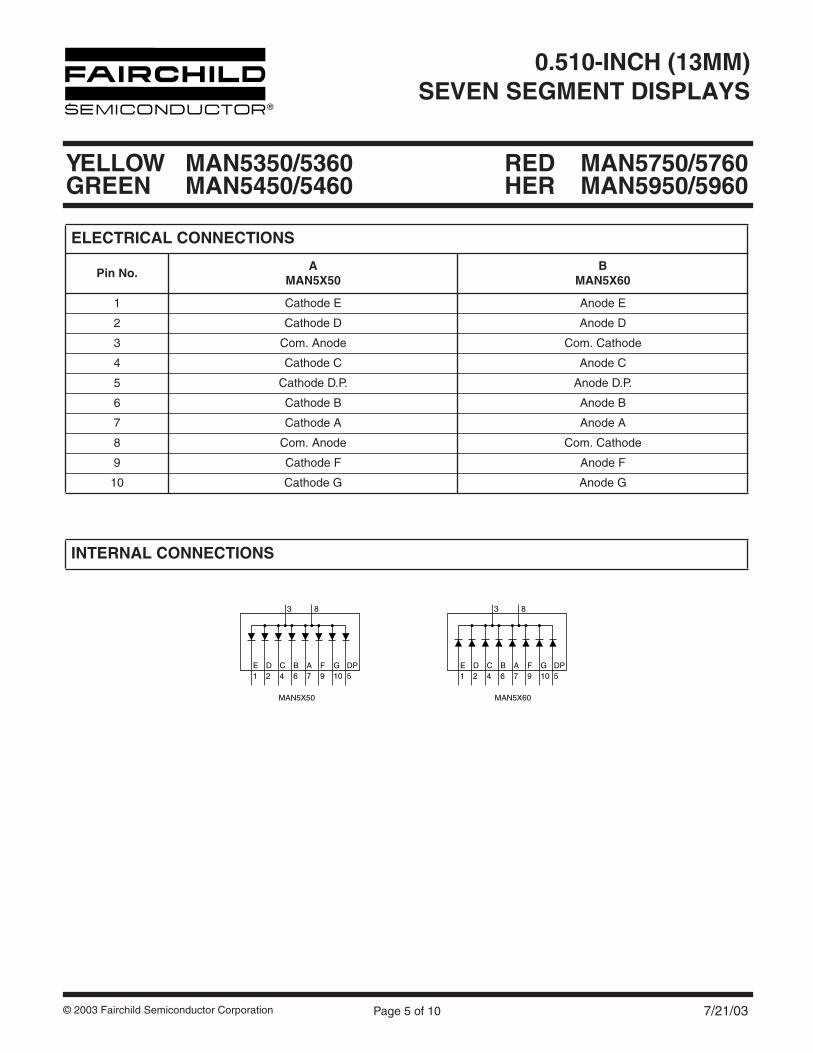
7/21/03
Page 5 of 10
© 2003 Fairchild Semiconductor Corporation
0.510-INCH (13MM)SEVEN SEGMENT DISPLAYS
YELLOW MAN5350/5360 RED MAN5750/5760GREEN MAN5450/5460 HER MAN5950/5960
ELECTRICAL CONNECTIONS
Pin No.A
MAN5X50B
MAN5X60
1 Cathode E Anode E
2 Cathode D Anode D
3 Com. Anode Com. Cathode
4 Cathode C Anode C
5 Cathode D.P. Anode D.P.
6 Cathode B Anode B
7 Cathode A Anode A
8 Com. Anode Com. Cathode
9 Cathode F Anode F
10 Cathode G Anode G
INTERNAL CONNECTIONS
3
MAN5X50 MAN5X60
E1
D2
C4
B6
A7
F9
G10
DP5
8 3
E1
D2
C4
B6
A7
F9
G10
DP5
8

7/21/03
Page 6 of 10
© 2003 Fairchild Semiconductor Corporation
0.510-INCH (13MM)SEVEN SEGMENT DISPLAYS
YELLOW MAN5350/5360 RED MAN5750/5760GREEN MAN5450/5460 HER MAN5950/5960
TYPICAL CHARACTERISTIC CURVES — MAN5350/MAN5360
5060708090
100
40302010
0
1.0
2.0
3.0
4.0
2.0
1.5
1
00 5 10 15 20 25 30 1.0
DC Forward Current – IF (mA)
Fig. 1A. Relative Luminous Intensityvs. DC Forward Current
VF (Volts)
Fig. 1B. Forward Current vs. Forward Voltage
Duty Cycle – %IF Per Seg 10 mA Average
Fig. 1E. Relative Luminous Intensity vs. Duty Cycle
Rel
ativ
e Lu
min
ous
Inte
nsity
I F -
mA
Rel
ativ
e In
tens
ity
2.0 3.00 4.0
10 20 40 DC
120
80
90
100
110
70
Ambient Temperature – °C
Fig. 1C. Relative Luminous Intensity vs. Temperature(See Note 2)
Rel
ativ
e B
right
ness
- %
-50 -25 0 25 50 70
1000
20
200
1008050
500800
10
Duty Cycle – %
Fig. 1D. Max Peak Current vs. Duty Cycle
Pea
k I F
- m
A
1 2 3 5 8 10 20 30 50 80 100
FREQUENCY = 200pps
NORMALIZED at IF = 10 mA

7/21/03
Page 7 of 10
© 2003 Fairchild Semiconductor Corporation
0.510-INCH (13MM)SEVEN SEGMENT DISPLAYS
YELLOW MAN5350/5360 RED MAN5750/5760GREEN MAN5450/5460 HER MAN5950/5960
TYPICAL CHARACTERISTIC CURVES — MAN5450/MAN5460
5060708090
100
40302010
0
1.0
2.0
3.0
4.0
600800
1000
200
400
406080
100
20
10
00 5 10 15 20 25 30 2.0
DC Forward Current – IF (mA)
Fig. 2A. Relative Luminous Intensityvs. DC Forward Current
Forward Voltage – VF (Volts)
Fig. 2B. Forward Current vs.Forward Voltage
Pulse Duration – µS
Fig. 2E. Maximum Peak Current vs. Pulse Duration
Rel
ativ
e Lu
min
ous
Inte
nsity
For
war
d C
urre
nt -
I F (
mA
)
Max
imum
Pea
k C
urre
nt -
mA
3.01.0 4.0
10 100 1000 10.000
130
90
100
110
120
70
80
Ambient Temperature – °C
Fig. 2C. Relative Luminous Intensity vs. Temperature(See Note 2)
Rel
ativ
e In
tens
ity –
%
-55 -25 0 25 50 75 100
4.0
1.0
2.0
3.0
0.0
Duty Cycle – %
Fig. 2D. Relative Efficiency vs. Duty Cycle
Rel
ativ
e E
ffici
ency
(IL
at d
rive/
I L a
t 10
mA
DC
)
2.0 5.0 10 20 50 DC
NORMALIZED at IF = 10 mA
NORMALIZED at 25°C
(Dotted LineIndicates Pulsed
Operation See Figs 2D, 2E)
IF (AVG) = 20 mA10 mA5 mA
2.5mA
10 KHz30 KHz
1.0 KHz
300 KHz
100 KHz

7/21/03
Page 8 of 10
© 2003 Fairchild Semiconductor Corporation
0.510-INCH (13MM)SEVEN SEGMENT DISPLAYS
YELLOW MAN5350/5360 RED MAN5750/5760GREEN MAN5450/5460 HER MAN5950/5960
TYPICAL CHARACTERISTIC CURVES — MAN5750/MAN5760
5060708090
100
40302010
0
1.0
2.0
3.0
4.0
2
1
00 5 10 15 20 25 30 5
DC Forward Current – IF (mA)
Fig. 3A. Relative Luminous Intensityvs. DC Forward Current
VF (Volts)
Fig. 3B. Forward Current vs. Forward Voltage
Percent Duty Cycle
Fig. 3E. Relative Luminous Intensity vs. Duty Cycle
Rel
ativ
e Lu
min
ous
Inte
nsity
I F -
mA
Rel
ativ
e In
tens
ity
10 150 20
10 20 40 DC
170
13012011010090807060
140150160
50
Ambient Temperature – °C
Fig. 3C. Relative Luminous Intensity vs. Temperature(See Note 2)
Rel
ativ
e B
right
ness
- %
-50 -25 0 25 50 70
1000
20
200
1008050
500800
10
Duty Cycle – %
Fig. 3D. Max Peak Current vs. Duty Cycle
Pea
k I F
- m
A
1 2 3 5 8 10 20 30 50 80 100
FREQUENCY = 200pps
NORMALIZED at IF = 10 mA

7/21/03
Page 9 of 10
© 2003 Fairchild Semiconductor Corporation
0.510-INCH (13MM)SEVEN SEGMENT DISPLAYS
YELLOW MAN5350/5360 RED MAN5750/5760GREEN MAN5450/5460 HER MAN5950/5960
TYPICAL CHARACTERISTIC CURVES — MAN5950/MAN5960
5060708090
100
40302010
0
1.0
2.0
3.0
4.0
2
1.5
1
00 5 10 15 20 25 30 4
DC Forward Current – IF (mA)
Fig. 4A. Relative Luminous Intensity vs. Forward Current
Forward Voltage – VF (Volts)
Fig. 4B. Forward Current vs. Forward Voltage
Duty Cycle – %IF Per Seg 10 mA Average
Fig. 4E. Relative Luminous Intensity vs. Duty Cycle
Rel
ativ
e Lu
min
ous
Inte
nsity
(IF)
- m
A
Rel
ativ
e In
tens
ity
8 1.20 1.6 2.0 2.4 2.8 3.2 3.6 4.0
10 20 40 DC
100110120130140150160170
60708090
50
Ambient Temperature – °C
Fig. 3C. Relative Luminous Intensity vs. Temperature(See Note 2)
Rel
ativ
e In
tens
ity –
%
-50 -25 0 25 50 70
1000
20
200
1008050
500800
10
Duty Cycle – %
Fig. 4D. Maximum Peak Current vs. Duty Cycle
Pea
k I F
– m
A
1 3 5 10 20 50 100
FREQUENCY = 200pps
NORMALIZED at IF = 10 mA

LIFE SUPPORT POLICY
FAIRCHILD’S PRODUCTS ARE NOT AUTHORIZED FOR USE AS CRITICAL COMPONENTS IN LIFE SUPPORT DEVICES OR SYSTEMS WITHOUT THE EXPRESS WRITTEN APPROVAL OF THE PRESIDENT OF FAIRCHILD SEMICONDUCTOR CORPORATION. As used herein:
1. Life support devices or systems are devices or systemswhich, (a) are intended for surgical implant into the body, or(b) support or sustain life, and (c) whose failure to performwhen properly used in accordance with instructions for useprovided in the labeling, can be reasonably expected toresult in a significant injury of the user.
2. A critical component in any component of a life supportdevice or system whose failure to perform can bereasonably expected to cause the failure of the life supportdevice or system, or to affect its safety or effectiveness.
DISCLAIMER
FAIRCHILD SEMICONDUCTOR RESERVES THE RIGHT TO MAKE CHANGES WITHOUT FURTHER NOTICE TO ANY PRODUCTS HEREIN TO IMPROVE RELIABILITY, FUNCTION OR DESIGN. FAIRCHILD DOES NOT ASSUME ANY LIABILITY ARISING OUT OF THE APPLICATION OR USE OF ANY PRODUCT OR CIRCUIT DESCRIBED HEREIN; NEITHER DOES IT CONVEY ANY LICENSE UNDER ITS PATENT RIGHTS, NOR THE RIGHTS OF OTHERS.
7/21/03
Page 10 of 10
© 2003 Fairchild Semiconductor Corporation
0.510-INCH (13MM)SEVEN SEGMENT DISPLAYS
YELLOW MAN5350/5360 RED MAN5750/5760GREEN MAN5450/5460 HER MAN5950/5960
Related Documents