Northumbria Research Link Citation: Haigh, Paul (2014) Using Equalizers to Increase Data Rates in Organic Photonic Devices for Visible Light Communications Systems. Doctoral thesis, University of Northumbria. This version was downloaded from Northumbria Research Link: http://nrl.northumbria.ac.uk/id/eprint/21415/ Northumbria University has developed Northumbria Research Link (NRL) to enable users to access the University’s research output. Copyright © and moral rights for items on NRL are retained by the individual author(s) and/or other copyright owners. Single copies of full items can be reproduced, displayed or performed, and given to third parties in any format or medium for personal research or study, educational, or not-for-profit purposes without prior permission or charge, provided the authors, title and full bibliographic details are given, as well as a hyperlink and/or URL to the original metadata page. The content must not be changed in any way. Full items must not be sold commercially in any format or medium without formal permission of the copyright holder. The full policy is available online: http://nrl.northumbria.ac.uk/policies.html

Welcome message from author
This document is posted to help you gain knowledge. Please leave a comment to let me know what you think about it! Share it to your friends and learn new things together.
Transcript

Northumbria Research Link
Citation: Haigh, Paul (2014) Using Equalizers to Increase Data Rates in Organic PhotonicDevices for Visible Light Communications Systems. Doctoral thesis, University ofNorthumbria.
This version was downloaded from Northumbria Research Link:http://nrl.northumbria.ac.uk/id/eprint/21415/
Northumbria University has developed Northumbria Research Link (NRL) to enable usersto access the University’s research output. Copyright © and moral rights for items onNRL are retained by the individual author(s) and/or other copyright owners. Single copiesof full items can be reproduced, displayed or performed, and given to third parties in anyformat or medium for personal research or study, educational, or not-for-profit purposeswithout prior permission or charge, provided the authors, title and full bibliographicdetails are given, as well as a hyperlink and/or URL to the original metadata page. Thecontent must not be changed in any way. Full items must not be sold commercially in anyformat or medium without formal permission of the copyright holder. The full policy isavailable online: http://nrl.northumbria.ac.uk/policies.html
Using Equalizers to Increase Data Ratesin Organic Photonic Devices for Visible
Light Communications Systems
Paul Anthony HaighFaculty of Engineering and Environment
Northumbria University
This dissertation is submitted for the degree of
Doctor of Philosophy
July 2014


To you, I dedicate this thesis. . .


Declaration
I hereby declare that except where specific reference is made to the work of others, thecontents of this thesis are original and have not been submitted in whole or in part forconsideration for any other degree or qualification in this, or any other university.
Paul Anthony HaighJuly 2014

Acknowledgements
Firstly, I would like to offer apologies in case I have missed anyone, this was certainly notintentional.
Secondly, before I move on to the individuals that have helped to shape my PhD andmade my studies such an enjoyable experience, I would like to acknowledge all financialsupport received, including a full university PhD scholarship and the multiple IEEE anduniversity grants that I have received for conference attendance and journal charges. I wouldalso like to acknowledge the financial support of the Hong Kong Polytechnic University formy secondment there. Furthermore, I would like to gratefully acknowledge the financialsupport of the European Union IC1101 COST program and the Technical University ofGraz, Austria for approving my short term scientific mission and supporting it financially.Finally I must acknowledge the support given to me by all of the research students, staff andadministrators that I came into contact during my PhD and also during my spell as a visitingresearcher at University College London.
The first person I would like to thank is my principle supervisor, Fary Ghassemlooywho has carefully guided me from a time before I even started my PhD, to the very endand beyond. Fary offered his full confidence, enthusiasm, support and belief in me at everyturn and this is reflected in the numerous collaborations that I established through my work.Without Fary I would not have had the opportunity to study for my PhD at such a young ageand I thoroughly understand the advantages and privileges from which I have benefited as adirect result of Fary’s confidence in me. Thank you sincerely, Fary.
Secondly, Ioannis Papakonstantinou has repeatedly gone above and beyond what is nec-essary to be an excellent supervisor; usually at the expense of his own time. I would liketo note the outstanding support that you have given me over the years, including our timetogether at CERN. Furthermore, the year I spent as a visiting researcher in your researchgroup at University College London (UCL) were some of the most productive days of myPhD. This was an exceptional platform to achieve some of the results shown in this thesis.Thank you for every opportunity you have given to me.
Thanks to Hoa Le Minh for supporting me through this work, especially at the earlystages of my PhD where you very elegantly helped to point me in the direction of visible

viii
light communications and offer substantial support throughout all of the stages of the work.To Sujan Rajbhandari, University of Oxford, thank you for being such a close friend
and colleague of mine throughout this work. I would suggest that without our time togetherspent in the laboratories, this work would have been substantially less enjoyable. I lookforward to a continuation of this in the future.
I am indebted to Sandro Francesco Tedde, Francesco Arca and Oliver Hayden of Cor-porate Technology, Siemens AG, Erlangen, Germany. I must thank each of you individuallynot only for the production of the organic photodetectors used in several chapters of thiswork and the continuous support over the duration of my PhD, but also for the individuallessons that you have all taught me. I have thoroughly enjoyed our collaboration and lookforward to future endeavours developing this technology together.
In my PhD I was able to collaborate closely with a number of colleagues, but none wasmore productive than my work with Francesco Bausi working with organic polymer diodesproduced in the Physics department of UCL. I have thoroughly enjoyed our work together inour respective laboratories, and particularly the personal aspect of this research and gettingto know you very well, which has been my privilege. This research was made possibleby Franco Cacialli, who helped to establish and support this work, whilst delivering hisinsight and knowledge to enable our rapid progress. I also look forward to our continuedcollaboration.
I offer special thanks to Lu Chao and Erich Leitgeb of Hong Kong Polytechnic Univer-sity and the Technical University of Graz, respectively who both supported my secondmentinto their groups at various stages of my PhD. I had a very good time both academically andsocially in both Hong Kong and Graz and look forward to meeting you again in the future.
Further thanks to Wasiu Popoola of Glasgow Caledonian University, for his excellentinput to improve the quality of work in the second half of my PhD work. I am sure that ourwork together will continue as productively as ever in the future.
I would like to offer sincere thanks to my internal and external examiners, Dr Xuewu Daiand Professor Izzat Darwazeh, respectively, for giving me a very thorough and professionalexamination platform that I ultimately enjoyed very much.
Sincere thanks must go to Andrew Bradley, to whom I owe a tremendous debt of grati-tude. You spent considerable time helping me in a hard time, and it is a direct result of thatinvestment that I have been able to come this far and complete this work, so thank you.
To James Savage, thank you very much for distracting me from the work at every op-portunity, and for honouring me by making me your best man.
Thanks to my parents and Helene, you already know how much I appreciate everythingyou have done for me.

Abstract
This thesis proposes to marry two separate technologies together. The first technology isthat of visible light communications (VLC), and the second is small molecule and polymerorganic photonic devices. These two technologies both offer outstanding potential in theirrespective fields of information communications and optoelectronics, with both being pro-posed as two of the most important technologies about to emerge in the next decades bytheir respective research communities. As such, it is imperative to investigate and analysethe performance of organic photonic devices in the context of VLC broadcasting networks.There have been no experimental results in the literature reporting on organic-VLC systemsuntil the work proposed in this thesis and therefore the focus is on improving transmissionspeeds.
The reason for this is that organic devices typically have bandwidths that are orders ofmagnitude smaller than inorganic devices, and hence improving the transmission speed tosimilar levels is the foremost challenge available to address. Therefore this work investigatesfour separate links to find the maximum capacity possible in each case:
1. A small molecule organic light emitting diode (OLED) as the transmitter, with aninorganic photodetector (PD) as the receiver.
2. An inorganic LED as the transmitter, with an organic PD (OPD) as the receiver.
3. An SMOLED as the transmitter, with an OPD as the receiver.
4. A polymer LED (PLED) as the transmitter, with an inorganic PD as the receiver.
The modulation schemes focused on were non-return-to-zero (NRZ) on-off keying (OOK)and pulse position modulation (PPM). The improvement in transmission speed using the ar-tificial neural network (ANN) (links 1 — 3) and least mean squares (link 4) equalizer ispresented here in terms of bit error rate (BER) performance in comparison to the unequal-ized case.
The key results presented in this work show that in spite of the relatively low bandwidths(hundreds of kHz), transmission speeds in the region of Mb/s can be comfortably achieved

x
using equalization techniques. The maximum transmission speeds demonstrated in thiswork are 2.7, 3.75, 1.15 and 10 Mb/s for links 1, 2, 3 and 4 in Chapters 4, 5, 6 and 7,respectively.

Table of contents
Table of contents xi
List of figures xv
List of tables xxiii
Nomenclature xxiii
1 Introduction 11.1 Introduction to Visible Light Communications . . . . . . . . . . . . . . . . 11.2 Problem Statement . . . . . . . . . . . . . . . . . . . . . . . . . . . . . . 121.3 Research Aims and Objectives . . . . . . . . . . . . . . . . . . . . . . . . 131.4 Original Contributions to Knowledge . . . . . . . . . . . . . . . . . . . . . 141.5 List of Publications and Awards . . . . . . . . . . . . . . . . . . . . . . . 16
1.5.1 Peer Reviewed Journal Papers . . . . . . . . . . . . . . . . . . . . 161.5.2 Peer Reviewed Conference Papers . . . . . . . . . . . . . . . . . . 17
1.6 Thesis Organization . . . . . . . . . . . . . . . . . . . . . . . . . . . . . . 18
2 Principles of Organic Photonic Devices 212.1 Introduction . . . . . . . . . . . . . . . . . . . . . . . . . . . . . . . . . . 212.2 Review of Conventional Semiconductors . . . . . . . . . . . . . . . . . . . 212.3 Photon Generation and Absorption . . . . . . . . . . . . . . . . . . . . . . 22
2.3.1 Radiative Recombination of Electrons and Holes . . . . . . . . . . 242.3.2 Equivalent Model of the Light Emitting Diode . . . . . . . . . . . 25
2.4 Photodetectors . . . . . . . . . . . . . . . . . . . . . . . . . . . . . . . . . 272.5 Organic Semiconductors . . . . . . . . . . . . . . . . . . . . . . . . . . . 31
2.5.1 Hybridization . . . . . . . . . . . . . . . . . . . . . . . . . . . . . 322.6 The Bulk Heterojunction . . . . . . . . . . . . . . . . . . . . . . . . . . . 382.7 Summary . . . . . . . . . . . . . . . . . . . . . . . . . . . . . . . . . . . 43

xii Table of contents
3 Principles of Visible Light Communications 453.1 Introduction . . . . . . . . . . . . . . . . . . . . . . . . . . . . . . . . . . 45
3.2 Modulation Schemes . . . . . . . . . . . . . . . . . . . . . . . . . . . . . 52
3.2.1 M-ary Pulse Amplitude Modulation . . . . . . . . . . . . . . . . . 52
3.2.2 L-ary Pulse Position Modulation . . . . . . . . . . . . . . . . . . . 58
3.2.3 Summary of Modulation Schemes . . . . . . . . . . . . . . . . . . 64
3.3 Equalization Theory . . . . . . . . . . . . . . . . . . . . . . . . . . . . . . 64
3.3.1 Equalization as an Information Theory Problem . . . . . . . . . . . 65
3.3.2 RC Equalizer . . . . . . . . . . . . . . . . . . . . . . . . . . . . . 67
3.3.3 Zero-Forcing Equalizer . . . . . . . . . . . . . . . . . . . . . . . . 69
3.3.4 Adaptive Linear Equalizer . . . . . . . . . . . . . . . . . . . . . . 72
3.3.5 Decision Feedback Equalizer . . . . . . . . . . . . . . . . . . . . . 79
3.3.6 Equalization as a Classification Problem . . . . . . . . . . . . . . . 79
3.4 Summary . . . . . . . . . . . . . . . . . . . . . . . . . . . . . . . . . . . 88
4 Visible Light Communications with Organic Light Emitting Diodes 914.1 Introduction . . . . . . . . . . . . . . . . . . . . . . . . . . . . . . . . . . 91
4.2 Communications Performance . . . . . . . . . . . . . . . . . . . . . . . . 97
4.2.1 On-Off Keying . . . . . . . . . . . . . . . . . . . . . . . . . . . . 99
4.2.2 Pulse Position Modulation . . . . . . . . . . . . . . . . . . . . . . 101
4.3 Equalization . . . . . . . . . . . . . . . . . . . . . . . . . . . . . . . . . . 104
4.4 Summary . . . . . . . . . . . . . . . . . . . . . . . . . . . . . . . . . . . 107
5 Visible Light Communications with Organic Photodetectors 1095.1 Introduction . . . . . . . . . . . . . . . . . . . . . . . . . . . . . . . . . . 109
5.2 Communications Performance . . . . . . . . . . . . . . . . . . . . . . . . 111
5.2.1 Test Setup and Artificial Neural Network . . . . . . . . . . . . . . 112
5.3 Results . . . . . . . . . . . . . . . . . . . . . . . . . . . . . . . . . . . . . 115
5.4 Multiple-Input Multiple-Output . . . . . . . . . . . . . . . . . . . . . . . . 118
5.5 Introduction . . . . . . . . . . . . . . . . . . . . . . . . . . . . . . . . . . 118
5.6 MIMO Theory . . . . . . . . . . . . . . . . . . . . . . . . . . . . . . . . 119
5.6.1 Transmitters . . . . . . . . . . . . . . . . . . . . . . . . . . . . . 119
5.6.2 Channel Matrix . . . . . . . . . . . . . . . . . . . . . . . . . . . . 121
5.6.3 Receiver . . . . . . . . . . . . . . . . . . . . . . . . . . . . . . . 122
5.7 Results . . . . . . . . . . . . . . . . . . . . . . . . . . . . . . . . . . . . . 126
5.8 Conclusion . . . . . . . . . . . . . . . . . . . . . . . . . . . . . . . . . . 128
Table of contents xiii
6 Visible Light Communications with All Organic Optoelectronic Components 1296.1 Introduction . . . . . . . . . . . . . . . . . . . . . . . . . . . . . . . . . . 1296.2 Organic Optoelectronic Devices . . . . . . . . . . . . . . . . . . . . . . . 1316.3 Test Setup . . . . . . . . . . . . . . . . . . . . . . . . . . . . . . . . . . . 1316.4 Results . . . . . . . . . . . . . . . . . . . . . . . . . . . . . . . . . . . . . 1346.5 Summary . . . . . . . . . . . . . . . . . . . . . . . . . . . . . . . . . . . 137
7 Visible Light Communications with Polymer Light-Emitting Diodes 1397.1 Introduction . . . . . . . . . . . . . . . . . . . . . . . . . . . . . . . . . . 1397.2 Production and Characterization of the PLEDs . . . . . . . . . . . . . . . . 1407.3 Experimental Test Setup and LMS Equalizer . . . . . . . . . . . . . . . . . 1457.4 Results . . . . . . . . . . . . . . . . . . . . . . . . . . . . . . . . . . . . . 1487.5 Conclusion . . . . . . . . . . . . . . . . . . . . . . . . . . . . . . . . . . 151
8 Conclusions and Future Work 1538.1 Conclusions . . . . . . . . . . . . . . . . . . . . . . . . . . . . . . . . . . 1538.2 Future Work . . . . . . . . . . . . . . . . . . . . . . . . . . . . . . . . . . 156
8.2.1 Discrete Multi-tone Modulation . . . . . . . . . . . . . . . . . . . 1568.2.2 Pixel Combining for SNR Improvement . . . . . . . . . . . . . . . 1568.2.3 Reduction of Pixel Size . . . . . . . . . . . . . . . . . . . . . . . . 156
References 159

List of figures
1.1 UK radio frequency spectrum showing significant overcrowding . . . . . . 2
1.2 Visible light in the electromagnetic spectrum in the context of other com-munications technologies . . . . . . . . . . . . . . . . . . . . . . . . . . . 3
1.3 White light generation from WPLED and RGBLED link topologies; notethat the beam profile is indicated in yellow for WPLED for enhanced visi-bility but in reality the emission is white . . . . . . . . . . . . . . . . . . . 6
1.4 Optical spectra of an RGBLED (data from [1]) and an WPLED (measuredusing ThorLabs CCS2000) . . . . . . . . . . . . . . . . . . . . . . . . . . 7
1.5 List of the most popular equalizers, adapted from [2] . . . . . . . . . . . . 8
1.6 The received solar spectrum with highlighted visible region; data obtainedfrom [3] . . . . . . . . . . . . . . . . . . . . . . . . . . . . . . . . . . . . 11
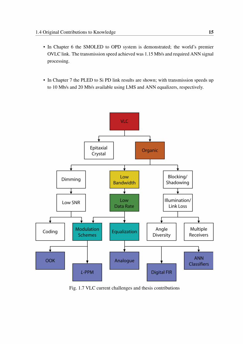
1.7 VLC current challenges and thesis contributions . . . . . . . . . . . . . . . 15
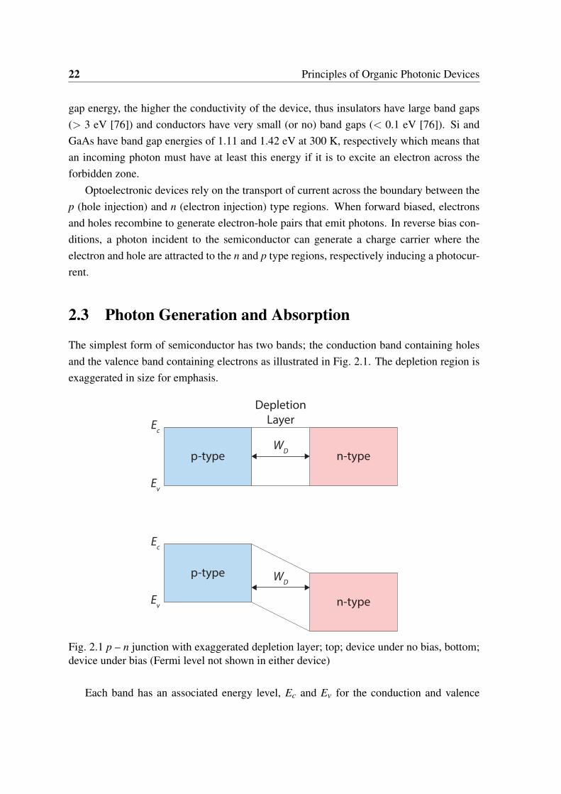
2.1 p – n junction with exaggerated depletion layer; top; device under no bias,bottom; device under bias (Fermi level not shown in either device) . . . . . 22
2.2 Electron hole pair generation and recombination . . . . . . . . . . . . . . . 23
2.3 Ideal Shockley equation showing the V-I relationship for a p - n junction . . 26
2.4 Theoretical p - n depletion layer capacitance as a function of area and width 27
2.5 Responsivity and band-gap energy of a number of semiconductor materials,abbreviations as follows; indium gallium arsenide (InGaAs), germanium(Ge), Si and P3HT; adapted from [4] and developed . . . . . . . . . . . . . 28
2.6 The structure of a PIN type photodetector . . . . . . . . . . . . . . . . . . 29
2.7 Ideal PD I-V relationship . . . . . . . . . . . . . . . . . . . . . . . . . . . 30
2.8 Equivalent model of a PIN PD; a first order RC low pass filter with twocurrent sources; the photocurrent Ip and the dark current Id . . . . . . . . . 30
2.9 Conductivity of some common organic polymers in comparison to commonmetal conductors and electrical insulators . . . . . . . . . . . . . . . . . . 33

xvi List of figures
2.10 Energy level diagram of bonding between two hydrogen atoms, electronspin is indicated by the arrows . . . . . . . . . . . . . . . . . . . . . . . . 34
2.11 Energy level diagram of π and σ bond generation by LCAO . . . . . . . . 352.12 Density of states for an organic semiconductor and the processes for pho-
ton emission with respect to the HOMO and LUMO levels; electrons andholes hope through localized states in the direction of the e− and h+ ar-rows in sections 1a and 1b, respectively. Trap states exist and the electronsand holes must avoid being restricted in these states to recombine to forma photon. In section 3 a Frenkel exciton is generated (bonding distance∼5 Å (1 Å = 1 × 10⁻¹⁰ m) [5]) and a photon is emitted . . . . . . . . . . . 37
2.13 The bulk heterojunction concept made up of electron acceptor and electrondonor including electron acceptor and electron donor materials, PCBM andP3HT, respectively . . . . . . . . . . . . . . . . . . . . . . . . . . . . . . 39
2.14 Top view of the OPD used in this thesis . . . . . . . . . . . . . . . . . . . 402.15 Bottom view of the OPD used in this thesis (four 1 cm2 diodes) . . . . . . . 402.16 Digital version of the OPD bottom view highlighting the key areas of the
device . . . . . . . . . . . . . . . . . . . . . . . . . . . . . . . . . . . . . 412.17 Shockley equation for an expanded p – n junction considering ideality factor
n; the influence of n is illustrated here - clearly for decreasing n the diodereaches the saturation current with less bias voltage which is advantageous . 42
3.1 Possible VLC link configurations - highlighted in red is the one used in thisthesis . . . . . . . . . . . . . . . . . . . . . . . . . . . . . . . . . . . . . 46
3.2 Block diagram of a typical indoor VLC link . . . . . . . . . . . . . . . . . 473.3 Lambertian emission profiles of several Lambertian orders . . . . . . . . . 483.4 Example L-I curve for intensity modulation of an optical source . . . . . . 493.5 Operation of matched filter; the data (top) is perturbed by noise (middle)
and the output of the matched filter (bottom) is much larger in magnitude incomparison to the noise level than the noisy signal (note the y-axis magni-tude), which is reflected in an increased SNR . . . . . . . . . . . . . . . . 51
3.6 Spectral efficiency of several modulation schemes as a function of SNR;all the modulation schemes are bound by the Shannon capacity where theuntenable region is highlighted with a dashed line . . . . . . . . . . . . . . 53
3.7 Transmitted waveforms for NRZ-OOK for the 1- and 0-levels . . . . . . . . 543.8 Bandwidth efficiency of M-PAM, recalling that 2-PAM is OOK . . . . . . . 543.9 Power spectral densities of M-PAM with box axes normalized to OOK . . . 553.10 OOK block diagram . . . . . . . . . . . . . . . . . . . . . . . . . . . . . . 56
List of figures xvii
3.11 Constellations for M-PAM . . . . . . . . . . . . . . . . . . . . . . . . . . 57
3.12 Probability of error curves for increasing orders of M-PAM . . . . . . . . . 58
3.13 Raw data code into the 4-PPM format with a comparison to OOK . . . . . 59
3.14 Bandwidth requirements for L-PPM, note that for L = 2 and L = 4 the re-quirement is identical . . . . . . . . . . . . . . . . . . . . . . . . . . . . . 60
3.15 PSDs of L-PPM; note that 2-PPM and 4-PPM have the same bandwidthrequirement . . . . . . . . . . . . . . . . . . . . . . . . . . . . . . . . . . 61
3.16 L-PPM block diagram with both soft and hard decision decoding . . . . . . 62
3.17 Probability of error curves for increasing orders of L-PPM . . . . . . . . . 63
3.18 General VLC block diagram with equalizer . . . . . . . . . . . . . . . . . 65
3.19 BLW for three different high pass filter cut-on frequencies . . . . . . . . . 69
3.20 Gaussian distribution of BLW . . . . . . . . . . . . . . . . . . . . . . . . 70
3.21 Normalized Optical Power Penalty for OOK, 4-PPM and 8-PPM; clearlyPPM has a better power penalty performance than OOK . . . . . . . . . . . 70
3.22 Zero forcing equalizer in linear transversal filter format; it should be notedthat the nomenclature yn is exactly the same as y(n) . . . . . . . . . . . . . 72
3.23 Adaptive linear transversal equalizer . . . . . . . . . . . . . . . . . . . . . 73
3.24 OOK link with linear 5-tap transversal equalizer . . . . . . . . . . . . . . . 78
3.25 Convergence on the error target using an LMS linear equalizer and varyingthe step-size, error cost function related to equation (3.52) . . . . . . . . . 80
3.26 RLS convergence speed with varying exponential forgetting factor, errorcost function related to equation (3.61) . . . . . . . . . . . . . . . . . . . . 80
3.27 Simple overview of a neuron . . . . . . . . . . . . . . . . . . . . . . . . . 83
3.28 Normalized threshold and piecewise linear activation functions . . . . . . . 84
3.29 Log-sigmoid activation function with α = 0.1 : 0.1 : 5 . . . . . . . . . . 84
3.30 Single layer ANN . . . . . . . . . . . . . . . . . . . . . . . . . . . . . . . 85
3.31 Multilayer ANN . . . . . . . . . . . . . . . . . . . . . . . . . . . . . . . . 85
3.32 Feedback ANN . . . . . . . . . . . . . . . . . . . . . . . . . . . . . . . . 86
3.33 Decision boundaries for two different classes based on different layer struc-tures, adapted from [6] . . . . . . . . . . . . . . . . . . . . . . . . . . . . 86
3.34 Local minima in error convergence during training; convergence is on globalminimum due to adaptive learning rate algorithm . . . . . . . . . . . . . . 87
3.35 Comparison of different ANN structures (1H = 1 hidden layer, 2H = 2 hid-den layers) and training schemes with SNR = 30 dB; the training length is1000 . . . . . . . . . . . . . . . . . . . . . . . . . . . . . . . . . . . . . . 88
xviii List of figures
4.1 Optical spectrum of the Osram Orbeos CMW-031 SMOLED under test withpeak wavelengths marked . . . . . . . . . . . . . . . . . . . . . . . . . . . 92
4.2 Polar plot showing the normalized measured emission profile of the SMOLED,which is in close agreement to the normalized Lambertian emission profile(m = 1) . . . . . . . . . . . . . . . . . . . . . . . . . . . . . . . . . . . . 92
4.3 Measurement setup for obtaining the SMOLED L-I-V curve . . . . . . . . 93
4.4 Measured SMOLED L-I-V curve for a range of bias currents over a periodof 12 hours . . . . . . . . . . . . . . . . . . . . . . . . . . . . . . . . . . 94
4.5 SMOLED bandwidth test measurement; the bias tee cut-on frequency is 7kHz while the Si PD bandwidth is 5 MHz (in 10 dB gain mode) as used inthis work . . . . . . . . . . . . . . . . . . . . . . . . . . . . . . . . . . . 94
4.6 Raw magnitude response of the SMOLED under test including large lowfrequency components introduced by the ESA, measured at point X in Fig. 4.5 95
4.7 Cut and normalized magnitude response of the SMOLED under test. Clearlythe bandwdith incraeses with bias voltage (and therefore injected current);the bandwidth in the best case is 98 kHz and in the worst case is 26 kHzgiving a difference of 72 kHz. The ratio of U/U0 on the y-axis refers to thenormalization against the first sample . . . . . . . . . . . . . . . . . . . . 96
4.8 Communications test setup for the SMOLED-VLC with a driver consistingof (a) a bias tee and (b) a NAND gate driver . . . . . . . . . . . . . . . . . 98
4.9 Measured SNR (red) (left), system bandwidth (BW) (blue) (right) and re-ceiver noise (black) (right) . . . . . . . . . . . . . . . . . . . . . . . . . . 99
4.10 BER performance of each driving circuit; data rates of 250 and 75 kb/s canbe achieved using the NAND gate and bias tee drivers, respectively . . . . . 100
4.11 Introduction of BLW from coupling capacitor of the bias tee . . . . . . . . 101
4.12 Eye diagram for bias tee driving circuit at 100 kb/s; there is a clear BLWeffect perturbing the link quality . . . . . . . . . . . . . . . . . . . . . . . 102
4.13 Eye diagram for the NAND gate driving circuit with a clear improvementover the bias tee driver . . . . . . . . . . . . . . . . . . . . . . . . . . . . 102
4.14 Unequalized BER performance of each modulation . . . . . . . . . . . . . 103
4.15 Soft decision BER performance of 2-PPM and 4-PPM where 400 and 200kb/s can be recovered, respectively . . . . . . . . . . . . . . . . . . . . . . 105

List of figures xix
4.16 Equalized BER performance of 2-PPM, OOK and 4-PPM in conjunctionwith the MLP-ANN in the MATLAB (M/L) domain, where data rates of2.7, 2.15 and 1.6 Mb/s can be achieved, respectively. Significantly, usingthe DSP MLP-ANN, data rates of 2.65, 2.15 and 1.5 Mb/s can be achievedfor the same modulation schemes which offer extremely good agreement ineach case . . . . . . . . . . . . . . . . . . . . . . . . . . . . . . . . . . . 106
5.1 EQE of the P3HT:PCBM OPD under test . . . . . . . . . . . . . . . . . . 1105.2 Responsivity of the P3HT:PCBM OPD under test in comparison to a Si PD 1105.3 OPD BWs for four light densities, varying from 10 to 300 µWcm−2 corre-
sponds to BWs ranging between 56−−160 kHz, giving ∼ 100 kHz range . 1115.4 Schematic system block diagram . . . . . . . . . . . . . . . . . . . . . . . 1145.5 BER performance for OOK and 4-PPM with and without ANN equalization 1165.6 BER performance of 4-PPM across the system with varying light density -
in each case, over 1 Mb/s can be supported . . . . . . . . . . . . . . . . . . 1175.7 MIMO system block diagram: The transmission side is controlled by Lab-
VIEW whereas the demodulation is performed in MATLAB . . . . . . . . 1205.8 Ch1 and Ch2 gain found using the histogram method . . . . . . . . . . . . 1235.9 Ch3 and Ch4 gain found using the histogram method . . . . . . . . . . . . 1235.10 (a) x− y plane and (b) x− y plane: the receiver plane divided into sections
S1-S9 for BER measurements . . . . . . . . . . . . . . . . . . . . . . . . 1245.11 Bottom view photograph of the OPD showing the spatial characteristics . . 1255.12 BW in the highest and lowest light densities on the receiving plane . . . . . 1255.13 Received Q-factor for section S7 with eye diagram inset at 50 kb/s; the
dashed line represents Q = 4.7, corresponding to a BER of 10−6 . . . . . . 1275.14 Aggregate BER and bit rate for the four key sections tested . . . . . . . . . 127
6.1 The L-I-V curve of the OLED under test with linear fitting; normalizedemission and absorption spectra of the OLED (blue) and OPD (red) respec-tively, noting that the vast majority of optical power is absorbed before thecut-off wavelength . . . . . . . . . . . . . . . . . . . . . . . . . . . . . . 132
6.2 Normalized and measured bandwidths of the OPD under test under differentcurrent bias conditions of the OLED, which control the light density . . . . 132
6.3 Block diagram of the experimental setup used in this work with ANN equal-izer implemented as a finite impulse response filter . . . . . . . . . . . . . 133
6.4 Unequalized BER and Q-factor of the high bandwidth link; 350 kb/s can berecovered at a BER of 10−5 . . . . . . . . . . . . . . . . . . . . . . . . . . 135
xx List of figures
6.5 Unequalized BER and Q-factor of the medium bandwidth link; 250 kb/s canbe recovered at a BER of 10−5 . . . . . . . . . . . . . . . . . . . . . . . . 135
6.6 Unequalized BER and Q-factor of the low bandwidth link; 150 kb/s can berecovered at a BER of 10−5 . . . . . . . . . . . . . . . . . . . . . . . . . . 136
6.7 Equalized BER performance of each of the three cases; data rates of 1100,850 and 450 kb/s can be recovered at a BER of 10−5 for the 135, 100 and65 kHz bandwidths, respectively . . . . . . . . . . . . . . . . . . . . . . . 137
7.1 A schematic of the PLED used in this work; the devices are composed ofa stack of several thin polymeric layers encapsulated between two planarelectrodes. The anode is a transparent conductive layer of ITO deposited ona glass substrate via a sputtering process. A hole injection layer made of aconjugated polymer poly(3,4-ethylenedioxythiophene) and poly(styrenesulfonate)(the mix is referred to as PEDOT:PSS) is in contact with the anode. On topof it, the conjugated polymer poly[(9’9’-dioctylfluorene-alt-N-(4-butylphenyl)diphenylamine](TFB) acts as electron-blocking/hole-transporting interlayer [7–9]. The emis-sive polymer poly[2-methoxy-5-(3’,7’-dimethyloctyloxy)-1,4-phenylenevinylene](MDMO-PPV) is deposited on top of the TFB and is in direct contact withthe metallic calcium cathode which is in turn covered by a layer of alu-minium as a protection against oxidation . . . . . . . . . . . . . . . . . . . 141
7.2 The energy-level diagram, relative to vacuum, of the isolated materials usedin the fabrication of the PLED. HOMO and LUMO stand for ’highest occu-pied molecular orbital’ and ’lowest unoccupied molecular orbital’ respec-tively. They indicate the two energy levels of the molecule that are respon-sible for its semiconductor behavior in the same way as valence and con-duction bands in inorganic semiconductors. The HOMO and LUMO valuesfor TFB and MDMO-PPV are measured by a combination of cyclic voltam-metry and optical absorption [10, 11]. The Fermi levels of the electrodesare also reported [12] . . . . . . . . . . . . . . . . . . . . . . . . . . . . . 142
7.3 Normalized PLED optical spectra and the responsivity of the ThorLabsPDA36A PD . . . . . . . . . . . . . . . . . . . . . . . . . . . . . . . . . 143
7.4 PLED JLV relationship, with VON at ∼2 V; note the semi-logarithmic axes . 143
7.5 The PLED current efficiency (cd/A) and external quantum efficiency (%) asa function of the current density . . . . . . . . . . . . . . . . . . . . . . . 144
7.6 The PLED the device frequency response for a variety of operating conditions144
7.7 Block diagram of the experimental test setup . . . . . . . . . . . . . . . . . 145

List of figures xxi
7.8 The system BER and Q-factor performance as a function of data rate; 3Mb/s can be achieved without the use of an equalizer. At 4 Mb/s the linkfails and errors are introduced into the system; eye diagrams are shown inset 149
7.9 The SNR measured throughout the system from 20 kHz – 1 MHz using anAgilent N9010A electrical spectrum analyser. The SNR is smoothed andfitted exponentially to predict the SNR at higher data rates . . . . . . . . . 149
7.10 BER performance of the PLED-VLC system with the FPGA based LMSequalizer; clearly there as an increase in performance with an increasingnumber of taps as expected; the key result is that the 10 Mb/s link has aBER within the FEC limit; meaning that the data can be recovered with anoverhead of just 7% . . . . . . . . . . . . . . . . . . . . . . . . . . . . . . 150


List of tables
3.1 Table comparing computer systems such as microprocessors or sequentiallogic with biological (and pseudo-biological) systems such as the neuralnetworks; adopted from [6, 13] . . . . . . . . . . . . . . . . . . . . . . . . 82

Chapter 1
Introduction
1.1 Introduction to Visible Light Communications
Due to the exponentially growing demand for data and bandwidth by the end-users, re-searchers are increasingly turning to optical communication technologies due to their broadbandwidths, licence free spectra and low implementation costs. The current UK radio fre-quency (RF) allocation chart is depicted in Fig. 1.1 (from [14]), which shows substantialovercrowding, leading to premium license fees and highly restricted bandwidth.
Optical wireless communications (OWC) is a subset under the wider optical communi-cation umbrella; which also consists of infra-red fibre, visible light communications (VLC),free-space communication (FSO) technologies [15]. Further communications technologiesinclude microwave technologies such as radar and RF as mentioned. Their spectrum alloca-tions are shown in Fig. 1.2 (adopted from adopted from [16]), where the visible wavelengthswith a bandwidth of ∼ 400 THz are highlighted; around 10,000 times higher than the RFbandwidth.
OWC operates in both the indoor and outdoor environments; with the indoor split intothree categories based on their operating wavelength; ultra-violet, visible light and infrared(IR) while the outdoor environment is colloquially known as FSO and mainly works in theIR region where the major challenge remains to be fog and other weather impediments [4].Indoor communications carried on the visible wavelengths (380 — 780 nm) is known asVLC and is a relatively new technology first proposed roughly a decade prior to this the-sis. VLC was first proposed as an alternative to indoor IR access technologies [17, 18]with a dual purpose of data communication and room illumination; transmission by meansof intensity modulation and direct detection (IM/DD) of a light-emitting diode (LED) andphotodetector(s) (PD), respectively. Development of the VLC technology was encouragedby rapid developments in gallium nitride (GaN) blue LED technologies that can be con-

2 Introduction
Part of the Chemring Group
Fig. 1.1 UK radio frequency spectrum showing significant overcrowding
verted to emit white light by coating the photoactive area with a yellowish cerium dopedyttrium aluminium garnet (Ce:YAG) phosphor, known as white phosphor LEDs (WPLEDs)[19–21]. The first reports of VLC using WPLEDs emerged from Japan via a series of con-ference publications [22–25] and it took several years before the first article was published[26]. Following this, the idea was popularized and the visible light communications con-sortium (VLCC) was established in Asia (i.e. Japan) in 2003, allowing technical discussionand collaboration between developers and for researchers working in the field. This lead tothe standardisation of VLC by the Institute of Electrical and Electronics Engineers (IEEE),namely IEEE 802.15.7 in 2012 [27] which outlines the individual layer standards requiredfor industrial implementation.
Data communications is the primary function of VLC and it is necessary to providefull connectivity regardless of the illumination level, which can easily be set using a directcurrent (DC) bias value. This leads to a further challenge considering the linearity of theLED electro-optic response; signal distortion can occur if the device is improperly biasedoutside of the linear region while the SNR is also degraded if the received optical poweris low. Most of the research aiming to tackle the dimming problem has focused on the

1.1 Introduction to Visible Light Communications 3
γ-rays X-rays Ultraviolet Infrared Microwave Radio Frequency
Fibre Optics &
Free Space Optics Microwave
& Radar RF Communications including Wi-Fi
x10,000
Fig. 1.2 Visible light in the electromagnetic spectrum in the context of other communicationstechnologies
modulation format selected. Pulse width modulation (PWM) is the standard way to controlthe average optical power output; by controlling the duty-cycle so that the required opticalpower level can easily be reached. The PWM signal does not carry any information though,and modulation schemes such as OOK, PPM and discrete multi-tone (DMT) have beenadded to the PWM signal to maintain information transmission at various illumination levels[28–36].
As mentioned the most popular type of LEDs used in VLC systems are WPLEDs be-cause of their simplicity, high optical power and reasonable bandwidth in the MHz regionafter phosphor conversion. At the receiver, it is possible to undo the effect of the phosphorand remove the yellowish wavelengths to recover the faster response of the GaN diode us-ing a short wavelength pass filter at the receiver (known colloquially as a blue filter). Thiscauses a significant challenge in VLC in terms of how to drive up the transmission speed,which has attracted widespread attention within the research community at large. The firstsignificant reports of high speed VLC systems using WPLEDs emerged based on introduc-ing resonant circuits matched to the frequency response of the transmitter in order to expandthe bandwidth and hence the transmission speed. The resonant drive circuit consists of threesub-drivers each with dissimilar resonant frequencies for equalizing different regions of thesystem frequency response. Using a single WPLED (2.5 MHz raw bandwidth) and OOK, an

4 Introduction
equalized bandwidth of 40 MHz was achieved leading to a transmission speed of 80 Mb/sat a BER of 10−6 [37]. In [38] this scheme was extended by introducing a 4 × 4 matrixof 16 WPLEDs with a drive circuit that resonates with the aggregate frequency responseof the WPLEDs. However the bandwidth achieved with such a configuration was reducedto 20 MHz with a transmission speed of 40 Mb/s, or a reduction by half in comparison to[37]. The reason for this reduction is not stated in either report; however the most likelycause for this is that the resonant matching in the single WPLED is much better than themultiple WPLEDs, thus offering a higher bandwidth. On the other hand, in [38] it is shownthat by introducing multiple WPLEDs the distance can be substantially improved to 0.5 m,compared to a back-to-back link scenario in [37].
Subsequently, a 100 Mb/s link (BER of 10−9) based on a WPLED was reported in [39]that offered a reduction in complexity over [37, 38] by removing the resonant circuits at thetransmitter. Instead, a single resistor-capacitor (RC) analogue high pass filter (HPF) wasintroduced at the receiver [39]. The raw bandwidth of the WPLED remains at 2.5 MHz,however in [39] a blue filter was introduced resulting in bandwidth of 14 MHz at the costof a 20 dB power penalty (at low frequencies). Using the HPF a bandwidth extension up to50 MHz is recorded with a transmission speed of 100 Mb/s [39]. However, there is a majordrawback using HPF equalization and that is the introduction of the baseline wander (BLW)phenomenon, which occurs when the low-frequency components of a baseband modulationformat are attenuated by the coupling capacitors and HPFs. In [39] the BLW effect is notinvestigated. Note that with a link using HPF and a simple threshold detector it would notbe possible to recover the low frequency component including the DC level. BLW has beenthoroughly investigated in the literature [40–42] and is commonly treated as random noisewith a Gaussian distributed noise variance. The low frequency power penalty increasesexponentially with increasing cut-on frequency [40].
Each of the passive equalization methods discussed here are not without drawbacks. Theperformance of each method is dependent on each of the components in the circuits andWPLED. Therefore a generalized solution cannot exist as each WPLED will have slightlydifferent characteristics while WPLEDs from different manufacturers will vary significantly,thus this solution is not optimum.
Alterative modulation formats can protect against BLW depending on the spectral allo-cation of the information. For instance PPM has a low spectral content at DC that decreaseswith an increasing order of bits per symbol. However, PPM has not emerged as a popularmodulation format for the highly bandlimited VLC because the bandwidth requirement in-creases exponentially with the modulation order and is at least twice that of OOK in the bestcase [43], thus undesirably offering a low spectral efficiency. An alternative frequency based
1.1 Introduction to Visible Light Communications 5
modulation is DMT modulation, the basis of which is the parallel transmission of multipleorthogonally spaced subcarriers (commonly called ‘tones’ in RF technologies) that allowshigh order complex modulations such as quadrature amplitude modulation (QAM). Com-plex modulation formats such as QAM are desirable because they have the same power andbandwidth requirements as pulse amplitude modulation (PAM) except with a spectral effi-ciency that is M times higher, where M is the modulation order [44]. Further, with DMT itis possible to load selected subcarriers with redundant information (i.e. those spaced aroundDC and the low frequencies), effectively nullifying the effect of BLW. In [45] a 1 Gb/s linkwith a WPLED is implemented based on DMT modulation, offering a tenfold improvementover [39], albeit with a higher white bandwidth of 30 MHz; around ten times higher than theblue filtered bandwidth in [39]. This is a significant aspect because it meant that there wasno need for any blue filtering due to the additional power penalty it would incur on the sys-tem frequency response and SNR. In order to improve the transmission speed further, twoadditional techniques were used: firstly adaptive bit loading was implemented. Adaptive bitloading consists of recording the SNR measurement of the system (i.e. the subtraction ofthe frequency response (dB) from the noise floor (dB)) and allocating a given number of bitsper symbol depending on the measured SNR. For instance, the theoretical relationship be-tween SNR and the error vector magnitude (EVM) for several orders of QAM can be foundin [46] and used to decide the appropriate SNR threshold levels. Doing this means that theindividual subcarriers are modulated by constellations that they have the required SNR totransmit, thus avoiding introducing errors into the system and allowing higher throughput.The second technique is adaptive power loading, which can be thought of as a very similarprocess as RC HPF equalization because it aims to distribute power across the spectrum bymeasuring the received power of each subcarrier and feeding back the information to thetransmitter. The transmitter than makes a decision about which subcarriers to redistributepower from based upon the SNR availability and requirements.
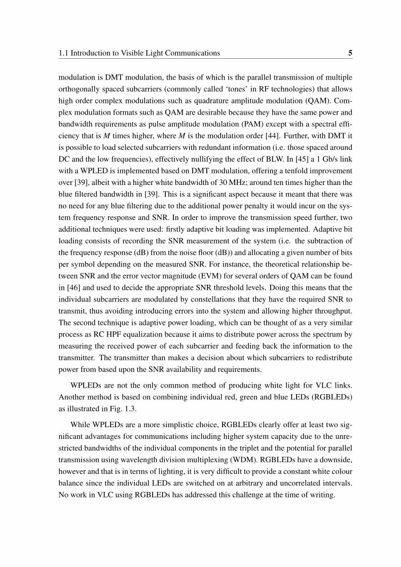
WPLEDs are not the only common method of producing white light for VLC links.Another method is based on combining individual red, green and blue LEDs (RGBLEDs)as illustrated in Fig. 1.3.
While WPLEDs are a more simplistic choice, RGBLEDs clearly offer at least two sig-nificant advantages for communications including higher system capacity due to the unre-stricted bandwidths of the individual components in the triplet and the potential for paralleltransmission using wavelength division multiplexing (WDM). RGBLEDs have a downside,however and that is in terms of lighting, it is very difficult to provide a constant white colourbalance since the individual LEDs are switched on at arbitrary and uncorrelated intervals.No work in VLC using RGBLEDs has addressed this challenge at the time of writing.

6 Introduction
Receiving Plane
Receiving Plane
RGBLED
WPLED
Fig. 1.3 White light generation from WPLED and RGBLED link topologies; note that thebeam profile is indicated in yellow for WPLED for enhanced visibility but in reality theemission is white

1.1 Introduction to Visible Light Communications 7
A comparison of the optical spectra of an RGBLED and a WPLED is shown in Fig. 1.4.The RGBLED has peaks at 450 (B), 520 (G) and 635 (R) nm. In WPLEDs, the GaNemission occurs at 445 nm while the Ce:YAG phosphor has a wide spectral emission peakingaround 555 nm (green).
1.0
0.8
0.6
0.4
0.2
0.0
No
rmalized
In
ten
sit
y (
a.u
.)
750700650600550500450400350
Wavelength (nm)
RGBLED WPLED
Fig. 1.4 Optical spectra of an RGBLED (data from [1]) and an WPLED (measured usingThorLabs CCS2000)
Research using RGBLEDs has simply expanded on the 1 Gb/s DMT link reported in[45]. The adaptive DMT modulation format is extended onto the three separate wavelengths,resulting in a gross transmission speed of 3.4 Gb/s [47], an approximate increase of threefoldas expected. The downside of such an adaptive DMT modulation format is the requirementto feed back the system frequency response to the transmitter in order to establish how todistribute the bits and power. VLC is inherently a half-duplex technology considering thetypical aesthetic layout of home and office solid state light (SSL) systems and there has beenstrong disagreement in the VLC community about a feedback medium and a lack of reportsproposing a fully duplex link. There are strong arguments that an RF antenna is suitable dueto the lower capacity of the uplink, whilst there is also a case for using an IR uplink. Bothhave built-in problems and as such neither provides a clear case for implementation. Thususing a modulation format that heavily depends on a feedback channel is not the optimum
8 Introduction
case and alternatives should be explored.Equalization is a well-established subject that has been extensively studied and is widely
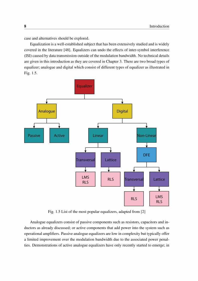
covered in the literature [48]. Equalizers can undo the effects of inter-symbol interference(ISI) caused by data transmission outside of the modulation bandwidth. No technical detailsare given in this introduction as they are covered in Chapter 3. There are two broad types ofequalizer; analogue and digital which consist of different types of equalizer as illustrated inFig. 1.5.
Equalizer
Analogue Digital
Non-LinearLinear
Lattice
DFE
Active
LatticeTransversal
Transversal
Passive
LMS
RLSRLS
RLSLMS
RLS
Fig. 1.5 List of the most popular equalizers, adapted from [2]
Analogue equalizers consist of passive components such as resistors, capacitors and in-ductors as already discussed; or active components that add power into the system such asoperational amplifiers. Passive analogue equalizers are low in complexity but typically offera limited improvement over the modulation bandwidth due to the associated power penal-ties. Demonstrations of active analogue equalizers have only recently started to emerge; in
1.1 Introduction to Visible Light Communications 9
[49] the first results are reported. The concept proposed is the same as the passive equaliz-ers except using an active filter. Thus it is possible to introduce additional power into thefrequency response, flattening the overall response whilst avoiding the attenuation of thelow frequencies. The transmission speed achieved with active equalization is 300 Mb/s at aBER of 10−9 [49].
Digital equalizers can be separated into linear and non-linear methods. Linear equalizersare less complex than non-linear equalizers at the cost of reduced BER performance (butmore complex than the analogue with better BER performance). Digital equalizers workon the principle of removing ISI by calculating the contribution of energy in the currentsymbol from previously transmitted symbols. Digital equalizers can make this estimationby comparing a known data sequence stored in memory with the received version of thesame sequence at the start of any transmission sequence, thus not requiring a feedback pathas in adaptive DMT. This is known as training and the estimation is made by updating a setof equalizer coefficients using an iterative method.
There is one additional type of equalizer that is not shown in Fig. 1.5 because it operatesin a different way. That is the ANN, which can be thought of as classifiers as opposed toa traditional equalizer because they classify a signal based on highly non-linear boundarieswhich are formed by an adaptive learning sequence.
Bearing in mind that OOK is the most commonly used modulation scheme in VLC andis compatible with digital equalizers, there is a noticeable lack of research in this area andthe only major reports are based on the analogue equalization as previously discussed. Anincrease in performance can be expected using digital equalizers but there are no reportsto provide any further results for a WPLED VLC system aside from [50]. Further, thereare no reports that provide any comparison between an adaptive DMT link and OOK withequalization, or an RGBLED with digital equalization.
A substantial problem with using either WPLEDs or RGBLEDs as the transmitter inVLC systems is scalability. LEDs produced with metal alloys such as GaN by epitaxialthermal evaporation methods result in brittle crystals that cannot easily be fashioned intolarge area panels which are desirable for VLC, SSL and other applications such as screensand displays. One possible solution to this is organic optoelectronic devices as a direct re-placement for WPLEDs and RGBLEDs, which offer low heat dissipation, mechanical flexi-bility, cheap production and arbitrarily large photoactive areas. Organic electroluminescentpolymers were first discovered by Burroughes in 1990 [51] and are now commonly knownas polymer LEDs (PLEDs). Alternatively, small molecule based organic electrolumines-cent devices known as small molecule organic LEDs (SMOLEDs) were proposed prior toPLEDs in 1987 by Tang and VanSlyke [52]. Aside from the length of molecules used in the
10 Introduction
semiconductor, PLEDs are more complex, based on long chains of π–conjugated polymers,the main difference between PLEDs and SMOLEDs is the processing method. SMOLEDsare generally thermal-vacuum evaporated while PLEDs can be solution processed which isthe cheaper (and thus more desirable) method.
Organic devices are based on thin film technology; the general structure for a photonicdevice is two or more organic semiconductor materials sandwiched by oppositely polarizedelectrodes. The most important manufacturing processes are solution processing [53], spraycoating [54], doctor blading [55], spin coating [56] and inkjet printing [57] all of whichare wet processed techniques that can offer potentially low mass production in the future.The total stack thickness for any OLED (either SMOLED or PLED) produced with anymanufacturing process is between 100 — 200 nm, which is a very exciting prospect forfuture displays, considering the common desire to miniaturise electronics as far as possible.
Aside from the transmitter, the receiver in VLC systems is also of the utmost importanceand is generally taken to be an individual positive-intrinsic-negative (PIN) Si PD [39], orless commonly, a Si avalanche PD (APD) [58]. Si PDs have responsivity in the rangeof 200 — 1100 nm and are very well established in free space optical communicationsoperating in the NIR wavelengths, where they offer high responsivity [4]. On the otherhand, the responsivity is very low in the visible range which is undesirable for VLC linkswhere the information is mostly carried on the blue wavelengths. Thus, additional opticalpower must be added in order to achieve a useful signal voltage level. It is not surprisingthat a dedicated material has not emerged for high speed, high responsivity PDs in thevisible range because previously no communications technology has utilized this region ofthe electromagnetic spectrum. Although solar cells typically operate in the visible regionwith reasonable efficiencies (refer to Fig. 1.6), they harvest the DC power and as such therehasn’t been any investigation into improving the bandwidths.
As most of the focus in VLC systems is focused on the transmitter and not on the re-ceiver, in spite of the drawbacks mentioned in the previous paragraph, OPDs (polymer-based) have emerged as an attractive prospect for VLC systems not only due to the low ma-terials costs (< £0.20/cm2 [59]) but also due to the fact that OPDs can be spray depositedwith higher efficiencies than Si [54] to different photoactive area devices. Furthermore, dueto the band gap energies of conjugated polymers (1 — 4 eV, encompassing the entire visiblerange); OPDs can be tailored for visible light whilst rejecting the entire IR region by carefulselection of the semiconductor materials.
The organic electronics sector is now large enough to be considered as a separate indus-try (the so-called printed electronics industry) to the Si electronics industry. According tomarket forecasters IDTechEx, the printed electronics industry will be valued at $330 billion

1.1 Introduction to Visible Light Communications 11
1.0
0.8
0.6
0.4
0.2
0.0
No
rmalized
In
ten
sit
y (
a.u
.)
300025002000150010005000
Wavelength (nm)
Visible Light The Sun
Fig. 1.6 The received solar spectrum with highlighted visible region; data obtained from [3]
as early as 2027 - more than the gross value of the Si market today ($225 billion) [60].
Organics are not without their disadvantages and challenges. The development of inor-ganics has been undertaken for a number of decades and homogenous devices can be pro-duced that are almost free from impurities and imperfections. This is not the case for organ-ics; every manufacturing process without exception introduces impurities and defects thatcan lead to charge traps and short circuits. Charge traps are poised to emerge as an extremelyimportant consideration in OVLC systems as the available device bandwidth is directly re-lated to filling traps with charge carriers [61]. Furthermore the charge transport mobility oforganics is around three orders of magnitude lower than amorphous Si [59]. It should benoted that this is due to highly disordered polymer crystallinity [62] which severely restrictsthe movement of charge carriers through the device, causing a bandwidth limitation. Thisis not the same problem as the Ce:YAG phosphor limiting device bandwidths because thatproblem can easily be solved using a short pass optical filter. As such this thesis takes onthis challenge with the aim of firstly introducing organic VLC (OVLC) systems and subse-quently achieving a high capacity using electronic equalization techniques.
Further, it is well known that inorganic LEDs are inherently non-linear devices and thisis reflected in their optical power – drive current – voltage (L-I-V) relationships. OLEDs

12 Introduction
exhibit the same non-linearity and the candidate proposed a model for an SMOLED in [63].The idea of organic photonics for communications had been conceived previously and
the first postulation of organic photonic devices for a communications system came in 1992[64] on organic optical fibre communications. A summary of potential organic communi-cations systems was outlined in [65], which raises some very important points. Perhaps themost crucial point is that organics should not be taken as a direct replacement for inorganicdevices, as such a transition will never occur due to the strong placement of inorganics inthe market and the cost of switching. On the other hand, [65] reports that organics shouldbe seen as a strong alternative technology for use in markets that inorganics cannot pene-trate. A good example of this would be an OVLC system where thin films and large areapanels are extremely desirable such as deployment in laptop computers, mobile phones andmultifunctional displays.
To date, research and development in organic communications systems has been limitedeven though reports are starting to emerge that allude to the prospect of organic opticalcommunications systems but they do not explicitly test important performance metrics suchas BER [65–70]. The root of this could be down to the fact that the device structure hasnot yet been optimized. For example the semiconductor interlayer influences the devicewavelength and charge transport characteristics, while the layer structure and organizationcan affect efficiency characteristics [71, 72].
1.2 Problem Statement
As introduced in the previous section, low charge transport mobility is a serious impedimentto high capacity OVLC systems because the devices simply cannot offer similar bandwidthsto IVLC systems. On the other hand, organics offer a variety of advantages that are ideallysuited to the applications of VLC; first and foremost the materials costs are extremely low(£0.20/cm2 for P3HT:PCBM) and can be dissolved into solvents that allow screen printingor spray deposition to produce large diodes that are simply impossible using inorganics.
As such, in this thesis organic devices are worthy of investigation as the transmitter andreceiver for VLC systems. A number of transmitter/receiver configurations are tested:
• A small molecule/polymer OLED as the transmitter and a Si PD as receiver.
• A WPLED as the transmitter and an OPD as the receiver.
• A completely OVLC system.
By adopting these configurations the maximum individual and collective potential of organicdevices can be found for VLC. As mentioned, the bandwidths of organics are significantly
1.3 Research Aims and Objectives 13
lower than their inorganic counterparts due to lower charge transport mobility, thus whenused for data communications the achievable data rates are highly restricted. If the trans-mission speed exceeds the modulation bandwidth of the system, ISI where the energy of theprevious pulses is carried over to the next pulses can be introduced into the system. Sub-sequently, equalization techniques are implemented in order to find the maximum bit ratesfor each topology. The overall results of each experiment will offer a first perspective onwhether or not organic photonic devices are suitable for VLC links using state-of-the-artcomponents.
1.3 Research Aims and Objectives
This work introduces a new domain to the VLC technology by using organic photonic com-ponents as the transmitter and receiver, respectively. This is an important developmentbecause of the cost reduction, large photoactive areas and increasing popularity of thin filmdevices in modern technologies, all of which are important for SSL and VLC equally. Ad-ditionally, establishing the OVLC domain has prompted research and developments frommany research groups throughout the world that are starting to build on the results reportedin this thesis, indicating the impact of this work.
The major challenge in using organic components as the optoelectronic devices in VLCsystems is the low charge transport mobility that leads to slow spontaneous recombinationof holes/electrons in the semiconductor and hence slow extinction of the luminescence andlow transmission bandwidths. Therefore a significant challenge remains to increase thetransmission speeds in OVLC systems. As a result three main themes will occur in thisthesis:
• Three OVLC topologies are proposed, experimentally investigated and demonstratedfor the first time:
– VLC with an SMOLED as the transmitter and a Si PD as receiver.
– A WPLED as the transmitter and an OPD as receiver.
– OVLC comprised of both an SMOLED and OPD.
– A PLED as the transmitter and a Si PD as receiver.
• OOK and PPM modulation schemes are tested due to their bandwidth and powerefficiencies, respectively.
• Due to low bandwidths, the suitability of a series of equalization methods to achievehigh data rates are investigated. The equalizers tested were:
14 Introduction
– Digital FIR equalizers as outlined previously.
– The ANN classifier implemented as an equalizer.
• Further, each equalizer has been implemented using an online filter on a Texas Instru-ments (TI) TMS320C6713 digital signal processing (DSP) board to ensure accurateperformance is reported where appropriate.
• Due to the nature of OPDs, which can be patterned arbitrarily, MIMO is experimen-tally demonstrated with a solitary OPD consisting of four diodes patterned on to thesame substrate.
The key achievement from these contributions was in each case to demonstrate megabitsper second (Mb/s) data rates using online equalization from system bandwidths in the kHzregion. This is a significant achievement for OVLC systems because it demonstrates thatthere is considerable potential in these systems. As the physical chemistry of organics im-proves to support higher charge transport properties, the bandwidths will improve and sub-sequently data rates will improve even further as is required for the optical backbone.
The key areas for research are highlighted in Fig. 1.7 where the coloured blocks indicatethe path taken through this work.
The outcome of this research demonstrated some extremely important results which arelisted next.
1.4 Original Contributions to Knowledge
The key contributions to knowledge that are derived in this thesis are as follows:
• In Chapter 4 the SMOLED to Si PD system is demonstrated and it is shown that agross transmission speed of 2.7 Mb/s can be achieved with a ∼90 kHz bandwidth,offering an increase in data rate over the raw bandwidth of ∼ 30 times. In order toachieve this result, an ANN equalizer was required and the modulation format wasOOK.
• In Chapter 5 the WPLED to OPD system is demonstrated, showing a gross trans-mission speed of 3.75 Mb/s with the same OOK and ANN equalizer topology as inChapter 4. As mentioned, the OPD has a dynamic bandwidth as a function of in-cident light density and the communications performance is outlined for a series ofbandwidths. The minimum transmission speed achieved is 1 Mb/s.
1.4 Original Contributions to Knowledge 15
• In Chapter 6 the SMOLED to OPD system is demonstrated; the world’s premierOVLC link. The transmission speed achieved was 1.15 Mb/s and required ANN signalprocessing.
• In Chapter 7 the PLED to Si PD link results are shown; with transmission speeds upto 10 Mb/s and 20 Mb/s available using LMS and ANN equalizers, respectively.
VLC
Epitaxial
CrystalOrganic
Low
Bandwidth
Blocking/
ShadowingDimming
Low
Data Rate
Illumination/
Link Loss
Angle
Diversity
Multiple
ReceiversEqualization
Modulation
Schemes
Analogue
Digital FIR
ANN
ClassifiersOOK
L-PPM
Low SNR
Coding
Fig. 1.7 VLC current challenges and thesis contributions

16 Introduction
1.5 List of Publications and Awards
1.5.1 Peer Reviewed Journal Papers
1. P. A. Haigh, F. Bausi, T. Kanesan, S. T. Le, S. Rajbhandari, Z. Ghassemlooy, I.Papakonstantinou, W. Popoola, A. Burton, H. Le Minh, A. D. Ellis and F. Cacialli,"A 20-Mb/s VLC link with a polymer LED and a multi-layer perceptron equalizer,"IEEE Photonics Technology Letters, vol. PP, 2014.
2. S. T. Le, T. Kanesan, F. Bausi, P. A. Haigh, S. Rajbhandari, Z. Ghassemlooy, I.Papakonstantinou, W. O. Popoola, A. Burton, H. Le Minh, F. Cacialli and A. D. Ellis,"10-Mb/s visible light transmission system using a polymer light-emitting diode withorthogonal frequency division multiplexing," Optics Letters vol. 39, pp. 3876-3879,2014.
3. P. A. Haigh, Z. Ghassemlooy, I. Papakonstantinou, F. Arca S. F. Tedde, O. Hayden,and E. Leitgeb, "A 1-Mb/s visible light communications link with low bandwidthorganic components," IEEE Photonics Technology Letters, vol. 26, pp. 1295-1298,2014.
4. P. A. Haigh, Z. Ghassemlooy, S. Rajbhandari, I. Papakonstantinou and W. Popoola,"Visible light communications: 170-Mb/s using an artificial neural network equalizerin a low bandwidth white light configuration," Journal of Lightwave Technology, vol.32, pp. 1807-1813, 2014.
5. P. A. Haigh, F. Bausi, Z. Ghassemlooy, I. Papakonstantinou, H. Le Minh, C. Fléchonand F. Cacialli, "Visible light communications: Real time 10-Mb/s link with a lowbandwidth polymer light-emitting diode," Optics Express, vol. 22, pp. 2830-2838,2014.
6. P. A. Haigh, Z. Ghassemlooy, S. Rajbhandari and I. Papakonstantinou, "Visible lightcommunications using organic light emitting diodes," IEEE Communications Maga-zine, vol. 51, pp. 148-154, 2013.
7. P. A. Haigh, Z. Ghassemlooy, I. Papakonstantinou and H. L. Minh, "2.7 Mb/s With a93-kHz White Organic Light Emitting Diode and Real Time ANN Equalizer," IEEEPhotonics Technology Letters, vol. 25, pp. 1687-1690, 2013.
8. S. Rajbhandari, P. A. Haigh, Z. Ghassemlooy and W. Popoola, "Wavelet-neural net-work VLC receiver in the presence of artificial light interference," IEEE PhotonicsTechnology Letters, vol. 25, pp. 1424-1427, 2013.

1.5 List of Publications and Awards 17
9. Z. Ghassemlooy, P. A. Haigh, F. Arca, S. F. Tedde, O. Hayden, I. Papakonstanti-nou and S. Rajbhandari, "Visible light communications: 3.75 Mb/s data rate with a160 kHz bandwidth organic photodetector and artificial neural network equalization[Invited]," Photonics Research, vol. 1, pp. 65-68, 2013.
10. P. A. Haigh, Z. Ghassemlooy and I. Papakonstantinou, "1.4-Mb/s white organic LEDtransmission system using discrete multi-tone modulation," IEEE Photonics Technol-ogy Letters, vol. 25, pp. 615-618, 2013.
11. P. A. Haigh, Z. Ghassemlooy, H. Le Minh, S. Rajbhandari, F. Arca, S. F. Tedde, O.Hayden and I. Papakonstantinou, "Exploiting equalization techniques for improvingdata rates in organic optoelectronic devices for visible light communications," Journalof Lightwave Technology, vol. 30, pp. 3081-3088, Oct 1 2012.
1.5.2 Peer Reviewed Conference Papers
1. P. A. Haigh, Z. Ghassemlooy, F. Bausi, I. Papakonstantinou, H. L. Minh, S. F. Tedde,O. Hayden and F. Cacialli, "Organic visible light communications: Recent progress[invited paper]," in IEEE ICTON 2014, Graz, Austria, 2014.
2. P. A. Haigh, F. Bausi, T. Kanesan, S. T. Le, S. Rajbhandari, Z. Ghassemlooy , I.Papakonstantinou, W. O. Popoola, A. Burton, H. Le Minh, A. D. Ellis and F. Cacialli,"A 10-Mb/s visible light communication system using a low bandwidth polymer light-emitting diode [invited]," in IEEE CSNDSP 2014, Manchester, UK, 2014.
3. P. A. Haigh, Z. Ghassemlooy, S. Rajbhandari and E. Leitgeb, "A 100-Mb/s visiblelight communications system using a linear adaptive equalizer," in Network and Op-tical Communications (NOC) and Optical Cabling and Infrastructure (OC&i) 2014,Milan, Italy, pp. [accepted], 2014.
4. P. A. Haigh, F. Bausi, Z. Ghassemlooy, I. Papakonstantinou, H. Le Minh, C. Flechonand F. Cacialli, "Next generation visible light communications: 10-Mb/s with polymerlight-emitting diodes," in Optical Fiber Communication Conference, San Francisco,California, 2014, p. Th1F.4.
5. P. A. Haigh, Z. Ghassemlooy, I. Papakonstantinou and S. Rajbhandari, "Online arti-ficial neural network equalization for a visible light communications system with anorganic light emitting diode based transmitter," in Network and Optical Communica-tions (NOC) and Optical Cabling and Infrastructure (OC&i) 2013, Graz, Austria, pp.153-158, 2013.

18 Introduction
6. P. A. Haigh, Z. Ghassemlooy, I. Papakonstantinou, F. Arca, S. F. Tedde, O. Haydenand S. Rajbhandari, "A MIMO-ANN System for Increasing Data Rates in OrganicVisible Light Communications Systems," in IEEE ICC 2013 - Wireless Communica-tions Symposium (ICC’13 WCS), Budapest, Hungary, 2013.
7. Z. Ghassemlooy, H. Le Minh, P. A. Haigh and A. Burton, "Development of Visi-ble Light Communications: Emerging Technology and Integration Aspects [InvitedPaper]," in OPTIC 2012, Taiwan, 2012.
8. A. Burton, H. Le Minh, Z. Ghassemlooy, S. Rajbhandari and P. A. Haigh, "Per-formance analysis for 180circ; receiver in visible light communications," in FourthInternational Conference on Communications and Electronics (ICCE), 2012, pp. 48-53.
9. A. Burton, H. Le Minh, Z. Ghassemlooy, S. Rajbhandari and P. A. Haigh, "Smartreceiver for visible light communications: Design and analysis," in 8th InternationalSymposium on Communication Systems, Networks & Digital Signal Processing (CSNDSP),pp. 1-5, 2012.
10. P. A. Haigh, T. T. Son, E. Bentley, Z. Ghassemlooy, H. Le Minh and L. Chao, "De-velopment of a Visible Light Communications System for Optical Wireless LocalArea Networks," in IEEE Computing, Communications and Applications Conference(ComComAp), pp. 351-355, 2012.
11. H. Le Minh, Z. Ghassemlooy, A. Burton and P. A. Haigh, "Equalization for OrganicLight Emitting Diodes in Visible Light Communications," in IEEE Globecom, Hous-ton, Texas, USA, 2011.
1.6 Thesis Organization
This thesis is organized as follows: in Chapter 2 a brief review of the theory of inorganicand organic semiconductors is presented and in Chapter 3 a review of the theory of commu-nications and equalization is given. In Chapter 4 the first original chapter is presented basedon the link BER evaluation of a SMOLED to Si PD system. It is found that a maximum 2.7Mb/s transmission speed can be supported. In Chapter 5 an original WPLED to OPD linkis evaluated in terms of BER performance and a 3.75 Mb/s link is demonstrated for the firsttime. In Chapter 7 a VLC link employing exclusively organic (SMOLED, OPD) optoelec-tronic components is discussed, including a transmission speed of 1.15 Mb/s. In Chapter 8

1.6 Thesis Organization 19
a PLED based VLC system is introduced and evaluated in terms of BER performance; firstdemonstrating that 10 Mb/s can be supported with an LMS equalizer and 20 Mb/s can besupported using an ANN.

Chapter 2
Principles of Organic Photonic Devices
2.1 Introduction
The theory of operation of inorganic semiconductors is well known and covered extensivelyin the literature [73], so is not repeated here in detail. This chapter discusses a basic out-line of electron/hole generation and recombination followed by the theory for some of theorganic photonic devices used in this work, based on availability of the structure from themanufacturers.
2.2 Review of Conventional Semiconductors
Semiconductors have electrically conductivity somewhere between a conductor such as cop-per often used in wires or an insulator like ceramic which can be commonly found insulatingpower lines. LEDs and PDs are based on the operation of semiconductor devices; hence itwill be useful to give a detailed review of the physics that is employed. Si and gallium (Ga)are two of the most important semiconductor materials in the fields of microelectronics andphotonics. In terms of light emitters, GaN has undergone something of a revolution overthe last few decades and now dominates the LED market due to high efficiency and highpower output [74, 75]. Gallium arsenide (GaAs) is generally heralded as the most impor-tant semiconductor material for light absorption due to its high responsivity in the IR range,but offers no detection in the visible range of the electromagnetic spectrum. On the otherhand, Si encompasses the entire visible to IR range, making it the most important inorganicsemiconductor material for VLC detectors, currently.
The reason for the difference in absorption wavelength is down to band theory. Thevalence and conduction bands are separated by the band gap energy. The smaller the band
22 Principles of Organic Photonic Devices
gap energy, the higher the conductivity of the device, thus insulators have large band gaps(> 3 eV [76]) and conductors have very small (or no) band gaps (< 0.1 eV [76]). Si andGaAs have band gap energies of 1.11 and 1.42 eV at 300 K, respectively which means thatan incoming photon must have at least this energy if it is to excite an electron across theforbidden zone.
Optoelectronic devices rely on the transport of current across the boundary between thep (hole injection) and n (electron injection) type regions. When forward biased, electronsand holes recombine to generate electron-hole pairs that emit photons. In reverse bias con-ditions, a photon incident to the semiconductor can generate a charge carrier where theelectron and hole are attracted to the n and p type regions, respectively inducing a photocur-rent.
2.3 Photon Generation and Absorption
The simplest form of semiconductor has two bands; the conduction band containing holesand the valence band containing electrons as illustrated in Fig. 2.1. The depletion region isexaggerated in size for emphasis.
Ec
Ev
p-type
n-type
WD
Ec
Ev
p-type n-typeW
D
Depletion
Layer
Fig. 2.1 p – n junction with exaggerated depletion layer; top; device under no bias, bottom;device under bias (Fermi level not shown in either device)
Each band has an associated energy level, Ec and Ev for the conduction and valence
2.3 Photon Generation and Absorption 23
bands, respectively and the band gap energy Eg is the difference between them:
Eg = Ec −Ev (2.1)
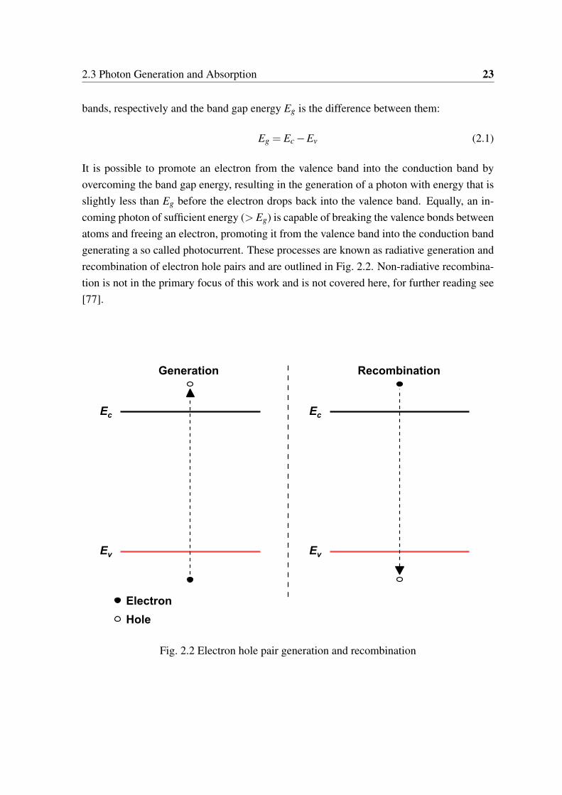
It is possible to promote an electron from the valence band into the conduction band byovercoming the band gap energy, resulting in the generation of a photon with energy that isslightly less than Eg before the electron drops back into the valence band. Equally, an in-coming photon of sufficient energy (> Eg) is capable of breaking the valence bonds betweenatoms and freeing an electron, promoting it from the valence band into the conduction bandgenerating a so called photocurrent. These processes are known as radiative generation andrecombination of electron hole pairs and are outlined in Fig. 2.2. Non-radiative recombina-tion is not in the primary focus of this work and is not covered here, for further reading see[77].
Ev
Ec
Ev
Ec
Electron
Hole
Generation Recombination
Fig. 2.2 Electron hole pair generation and recombination
24 Principles of Organic Photonic Devices
2.3.1 Radiative Recombination of Electrons and Holes
Without the influence of a bias voltage, at a given temperature the concentrations of holesp0 and electrons n0 are equal to the intrinsic carrier concentration ni, that is [77]:
n2 = n0 p0 (2.2)
In the presence of a bias voltage the concentration of charge carriers is given by [77, 78]:
n = n0 +δn (2.3)
p = p0 +δ p (2.4)
where δn and δ p are the excess charge carriers generated proportional to the bias voltage.As previously mentioned, the concentration of each type of charge carrier is not necessarilyequal. The recombination rate is directly proportional to the charge carrier concentrationsand the relationship is given by the bimolecular rate equation for light emitting diodes asfollows [77, 78]:
R = Bnp (2.5)
where B is the bimolecular recombination coefficient (cm3 s−1), given by [77]:
B = 3×10⁻¹⁰(
300T
)3/2( Eg
1.5
)2
(2.6)
Assuming either an n- or p-type semiconductor, the majority carrier concentration greatlyexceeds the injected concentration (i.e. δn ≪ (n0 + p0) or δ p ≪ (n0 + p0)) then the fol-lowing is obtained, assuming δn = δ p because generation and recombination occur in pairs[77, 78]:
R = B(n0 + p0 +δn)δn (2.7)
The radiative lifetime is given by [77]:
τli f etime ≃1
B(n0 + p0 +δn)(2.8)
which gives the carrier lifetime τli f etime for any p - n junction semiconductor. For highlevel injection such as modern high powered LEDs [79] and semiconductor lasers [78] theinjected concentration of charge carriers is far in excess of the majority charge carriers (i.e.
2.3 Photon Generation and Absorption 25
δn ≫ (n0 + p0) or δ p ≫ (n0 + p0)):
Rsp ≃ Bδn2 ≃ Bn2 (2.9)
The recombination rate for high level injection is called the spontaneous recombination rateRsp and is commonly associated with LEDs. Laser diodes are also subject to this recom-bination as well as stimulated emission of photons, which can be referred to in [77]. Therecombination rate is of the utmost importance in optical communications because it is oneof the main parameters controlling LED bandwidth [77].
In VLC systems (described in Chapter 4) the carrier lifetime is not something that canbe explicitly controlled since the LEDs are typically commercial devices; however it isnecessary to understand the origin of this phenomenon in order to understand the devicelimitations. The key method to overcome the carrier lifetime limitations in optical commu-nications is to model the device as an equivalent RC circuit (for simplicity). Both LEDs andPDs can be modelled as filters with low pass transfer functions.
2.3.2 Equivalent Model of the Light Emitting Diode
The Shockley diode equation describes the current - voltage relationship of LEDs and isgiven by [80]:
J = J0
[e
qVBkBT −1
](2.10)
where J0 is the saturation current density which has an expression given in [73], q is thecharge of an electron, VB is the bias voltage, kB is the Boltzmann constant and T is thetemperature (K). The Shockley equation is illustrated in Fig. 2.3 where the voltage normal-ization factor is qVB/kBT . The forward bias region is where LEDs operate. The reverse biasregion is for PDs which is discussed in the next section.
An LED is a p - n junction and therefore has a depletion region with width WD given by[77]:
WD =
√2εrε0(VD −VB)(N+
A +N−D )
qN+A N−
D(2.11)
where εr is the dielectric constant of the material,ε0 is the relative permittivity of a vacuum,N+
A and N−D is the concentration of acceptor and donor atoms, respectively and VD is the
diffusion voltage given in [77]. Taking the charge carrier parameters as constant at any

26 Principles of Organic Photonic Devices
15
10
5
0
-5
J/J
0 (
a.u
.)
-4 -2 0 2 4
Normalized Voltage (a.u.)
Reverse Bias Region-Js
Forwards BiasRegion
Ideal Shockley Equation
Fig. 2.3 Ideal Shockley equation showing the V-I relationship for a p - n junction
instantaneous time, clearly the width of the depletion region is related to the differencebetween the diffusion voltage and the bias voltage. If the bias voltage is negative the widthincreases and charge carriers require more energy to cross the semiconductor; this is a goodcondition for PDs and is known as reverse bias. While a positive bias voltage (forward bias)reduces the width and means that less energy is required for the charge carriers to diffuse,clearly a desirable condition for LEDs.
The capacitance of the depletion layer C j (F) is given by [81]:
C j =εε0
WD=
√εε0qN+
A N−D
2(VD −VB)(N+A +N−
D )(2.12)
which by inspection is similar to the expression for parallel plate capacitance, thus intro-ducing a term for the cross sectional area AD (m2), the junction capacitance becomes:
C j =εε0AD
WD(2.13)
The plate capacitance of silicon (dielectric constant 11.7) is illustrated in Fig. 2.4.Recalling that charge carriers have a definite and finite lifetime, it is clear that devices
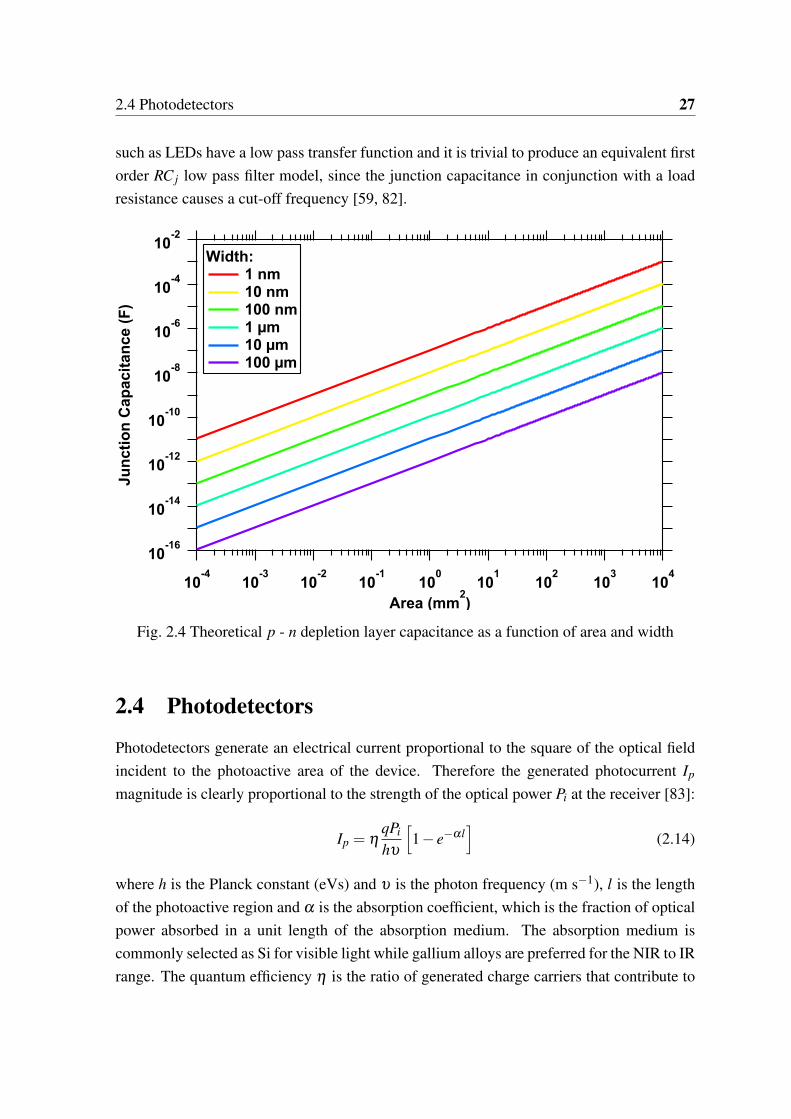
2.4 Photodetectors 27
such as LEDs have a low pass transfer function and it is trivial to produce an equivalent firstorder RC j low pass filter model, since the junction capacitance in conjunction with a loadresistance causes a cut-off frequency [59, 82].
10-16
10-14
10-12
10-10
10-8
10-6
10-4
10-2
Ju
nc
tio
n C
ap
ac
ita
nc
e (
F)
10-4
10-3
10-2
10-1
100
101
102
103
104
Area (mm2)
Width: 1 nm 10 nm 100 nm 1 µm 10 µm 100 µm
Fig. 2.4 Theoretical p - n depletion layer capacitance as a function of area and width
2.4 Photodetectors
Photodetectors generate an electrical current proportional to the square of the optical fieldincident to the photoactive area of the device. Therefore the generated photocurrent Ip
magnitude is clearly proportional to the strength of the optical power Pi at the receiver [83]:
Ip = ηqPi
hυ
[1− e−αl
](2.14)
where h is the Planck constant (eVs) and υ is the photon frequency (m s−1), l is the lengthof the photoactive region and α is the absorption coefficient, which is the fraction of opticalpower absorbed in a unit length of the absorption medium. The absorption medium iscommonly selected as Si for visible light while gallium alloys are preferred for the NIR to IRrange. The quantum efficiency η is the ratio of generated charge carriers that contribute to
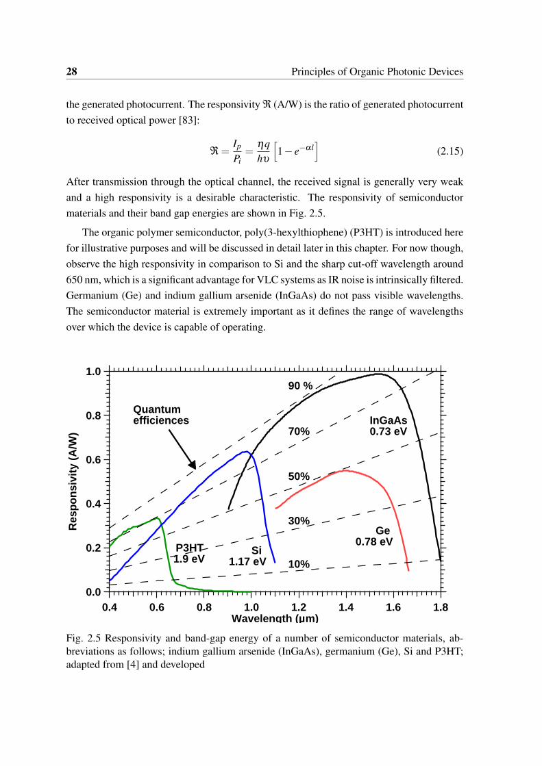
28 Principles of Organic Photonic Devices
the generated photocurrent. The responsivity ℜ (A/W) is the ratio of generated photocurrentto received optical power [83]:
ℜ =Ip
Pi=
ηqhυ
[1− e−αl
](2.15)
After transmission through the optical channel, the received signal is generally very weakand a high responsivity is a desirable characteristic. The responsivity of semiconductormaterials and their band gap energies are shown in Fig. 2.5.
The organic polymer semiconductor, poly(3-hexylthiophene) (P3HT) is introduced herefor illustrative purposes and will be discussed in detail later in this chapter. For now though,observe the high responsivity in comparison to Si and the sharp cut-off wavelength around650 nm, which is a significant advantage for VLC systems as IR noise is intrinsically filtered.Germanium (Ge) and indium gallium arsenide (InGaAs) do not pass visible wavelengths.The semiconductor material is extremely important as it defines the range of wavelengthsover which the device is capable of operating.
1.0
0.8
0.6
0.4
0.2
0.0
Res
pons
ivity
(A
/W)
1.81.61.41.21.00.80.60.4Wavelength (µm)
90 %
50%
70%
30%
10%
Quantumefficiences InGaAs
Ge
SiP3HT
0.73 eV
0.78 eV
1.17 eV1.9 eV
Fig. 2.5 Responsivity and band-gap energy of a number of semiconductor materials, ab-breviations as follows; indium gallium arsenide (InGaAs), germanium (Ge), Si and P3HT;adapted from [4] and developed

2.4 Photodetectors 29
An incident photon must have at least enough energy to overcome the band gap, gener-ating an electron-hole pair. The upper cut-off wavelength λc (m) can be found using Eg andis given by [73]:
λc =hcEg
=1.24×10⁻⁶
Eg(2.16)
Most PDs used in optical communications are not p – n junctions because the RC j timeconstant is large and there is low optical absorption in the diffusion lengths [78]. An intrinsiclayer is introduced as the major absorber in order to aid the absorption in comparison top – n junctions. PINs have the structure shown in Fig. 2.6, where Vb is in reverse biasconfiguration and RL is the load resistor.
p i n
RL
Ip
+ -
Fig. 2.6 The structure of a PIN type photodetector
The Shockley equation (Equation (2.10) is used to plot the I-V relationship of PDs, aswell as LEDs and examples of the dark and illumination current can be seen in Fig. 2.7. Areverse bias is required in order to ensure that the active region is absent of charge carri-ers. PINs consist of a wide intrinsic semiconductor with p-type and n-type material regions.Increasing the reverse bias voltage causes an increase in the intrinsic region width; thuscausing an decrease in capacitance and a higher bandwidth (refer to Fig. 2.4). The band-width of most PDs is limited by the combination of several parameters.
The most important are the resistor-capacitor (RC j) time constant and charge carrier

30 Principles of Organic Photonic Devices
lifetime as has been demonstrated previously. The PIN structure can be thought of as sim-ilar to the p – n junction however with a larger depletion region (the intrinsic region) andtherefore the mathematics of charge carrier transport through the device remains the same[78]. The equivalent circuit is therefore still low pass, however since the absorbed photonsare generating the photocurrent, at least one current source must be included to indicate thephotocurrent and the dark current as illustrated in Fig. 2.8.
-15
-10
-5
0
5
10
15
Cu
rren
t (a
.u.)
-10 -8 -6 -4 -2 0 2 4
Normalized Voltage (a.u.)
Reverse Bias Region
Forwards BiasRegion
JP
Photodetector: Ideal Dark Current Ideal Illumination Current
Fig. 2.7 Ideal PD I-V relationship
Ip
VOCRI
d
Fig. 2.8 Equivalent model of a PIN PD; a first order RC low pass filter with two currentsources; the photocurrent Ip and the dark current Id
The noise source in a PD is of crucial importance because it imposes the device lower
2.5 Organic Semiconductors 31
sensitivity limit. The main noise sources are shot IS and thermal IT (also called Johnson)noise, while there is also a contribution from the 1/ f noise I f which isn’t covered here [5]:
Inoise =√
I2S + I2
T + I2f (2.17)
As opposed to thermal noise, which is introduced by thermal fluctuations in the passivecomponents within the electronic circuitry the shot noise is introduced by fluctuations in thecurrent flow. Shot noise is given by [5]:
IS =√
2qId∆ f (2.18)
where ∆ f is the noise bandwidth. Thermal noise is given by [5]:
IT =
√4kT
R∆ f (2.19)
The noise equivalent power (NEP) is another important noise metric that is defined as theoptical power required to produce a photocurrent equal to the total noise current [5]:
NEP =Inoise
ℜ(2.20)
The NEP is clearly dependent on the physical characteristics of the PD such as the respon-sivity and also the frequency of the incoming signal. A small area device yields a lowerNEP value which is desirable.
2.5 Organic Semiconductors
A semiconductor is considered organic if the materials are mainly made up of either car-bon or nitrogen [5]. Organic semiconductors are a unique category of materials becausethey possess similar properties to metallic semiconductors and polymers simultaneously.They can offer electronic characteristics as previously discussed whilst offering superiormechanical and processing characteristics including mechanical flexibility, a variety of flex-ible substrates and low cost manufacturing. These attributes are extremely attractive forfuture electronics and a new type of industry is beginning to emerge; organic electronics.Within the organic electronics domain, a wide variety of applications is starting to emerge.The most popular are OLEDs and also organic solar cells (OPVs) and there is enormouspotential to provide extremely large scale general electronics at low cost. The first com-pletely organic microcontroller was recently reported in [84] that offers a fully functional
32 Principles of Organic Photonic Devices
8-bit flexible interface based on 3381 transistors. In comparison to the microcontrollers oftoday, where the number of transistors has scaled up into the billions approximately accord-ing to Moore’s law [85] (the Intel i7 has ∼ 1.4 billion transistors on-chip) this is a very smallamount. However, when the organic microcontroller is compared with the 4-bit Intel 4004which was one of the first examples of a Si microcontroller in 1971, the number of tran-sistors is ∼ 50% higher and the power consumption is reduced by five orders of magnitude[84] which demonstrates considerable potential.
The conductivities of some of the most common conductive polymers are shown inFig. 2.9 along with the molecular structure where appropriate. As can be seen, the con-ductivities of such materials are orders of magnitude lower than metal conductors whichare a serious impediment to high speed devices. A polymer is created by a reaction be-tween neighbouring atoms causing energy to be released and mixing between orbitals, orthe so-called hybridization of orbitals. The fine details of hybridization can be obtainedfrom [5, 86] with a general outline presented here.
2.5.1 Hybridization
Hybridization causes the bonds between molecules. After polymer formation has occurredit is not possible to describe the position of any single atom, and hence delocalized densitiesof electrons must be considered which are known as π-bonds which are weak due to theirelectron dislocation. There is also σ -bonds where the atomic location of each bondingelectron can be known; hence σ -bonds are far stronger than π-bonds so it is easier to procurean electron from the latter [5, 86].
Linear Combination of Molecular Orbitals
The previous discussion only concerns the orbitals of individual atoms. In order to under-stand the behaviour of molecules, it is necessary to perform the linear combination of atomicorbitals (LCAO). LCAO means adding the two atomic orbitals to form a bonding and anti-bonding orbital for the overall molecule. Atomic orbitals have phase in exactly the sameway as a standing wave. Combination of out-of-phase orbitals produces an anti-bondingorbital while combining two in-phase orbitals produces a bonding orbital. An anti-bondingorbital contains no electrons between the nuclei of the adjoined atoms aiding the repulsionmechanism between positively charged nuclei, thus raising the relative energy level in com-parison to the unbounded molecules. A bonding orbital is the opposite; electrons can befound between the nuclei of the two atoms and therefore a drop in relative energy level oc-curs as the electrons are shared. This concept can be illustrated in an energy level diagram
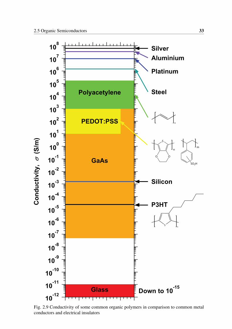
2.5 Organic Semiconductors 33
S
O O
n
SO2H
m
n
Sn
Fig. 2.9 Conductivity of some common organic polymers in comparison to common metalconductors and electrical insulators
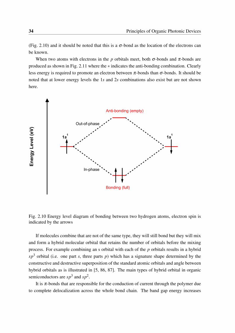
34 Principles of Organic Photonic Devices
(Fig. 2.10) and it should be noted that this is a σ -bond as the location of the electrons canbe known.
When two atoms with electrons in the p orbitals meet, both σ -bonds and π-bonds areproduced as shown in Fig. 2.11 where the ∗ indicates the anti-bonding combination. Clearlyless energy is required to promote an electron between π-bonds than σ -bonds. It should benoted that at lower energy levels the 1s and 2s combinations also exist but are not shownhere.
En
erg
y L
ev
el
(eV
)
1s1
1s1
Out-of-phase
In-phase
Anti-bonding (empty)
Bonding (full)
Fig. 2.10 Energy level diagram of bonding between two hydrogen atoms, electron spin isindicated by the arrows
If molecules combine that are not of the same type, they will still bond but they will mixand form a hybrid molecular orbital that retains the number of orbitals before the mixingprocess. For example combining an s orbital with each of the p orbitals results in a hybridsp3 orbital (i.e. one part s, three parts p) which has a signature shape determined by theconstructive and destructive superposition of the standard atomic orbitals and angle betweenhybrid orbitals as is illustrated in [5, 86, 87]. The main types of hybrid orbital in organicsemiconductors are sp3 and sp2.
It is π-bonds that are responsible for the conduction of current through the polymer dueto complete delocalization across the whole bond chain. The band gap energy increases
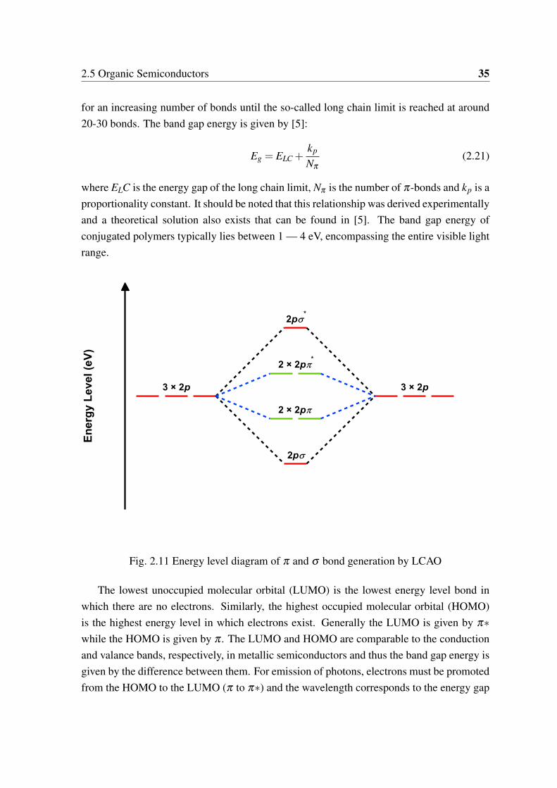
2.5 Organic Semiconductors 35
for an increasing number of bonds until the so-called long chain limit is reached at around20-30 bonds. The band gap energy is given by [5]:
Eg = ELC +kp
Nπ
(2.21)
where ELC is the energy gap of the long chain limit, Nπ is the number of π-bonds and kp is aproportionality constant. It should be noted that this relationship was derived experimentallyand a theoretical solution also exists that can be found in [5]. The band gap energy ofconjugated polymers typically lies between 1 — 4 eV, encompassing the entire visible lightrange.
En
erg
y L
ev
el
(eV
)
3 × 2p 3 × 2p
2 × 2pp*
2 × 2pp
2ps
2ps*
Fig. 2.11 Energy level diagram of π and σ bond generation by LCAO
The lowest unoccupied molecular orbital (LUMO) is the lowest energy level bond inwhich there are no electrons. Similarly, the highest occupied molecular orbital (HOMO)is the highest energy level in which electrons exist. Generally the LUMO is given by π∗while the HOMO is given by π . The LUMO and HOMO are comparable to the conductionand valance bands, respectively, in metallic semiconductors and thus the band gap energy isgiven by the difference between them. For emission of photons, electrons must be promotedfrom the HOMO to the LUMO (π to π∗) and the wavelength corresponds to the energy gap
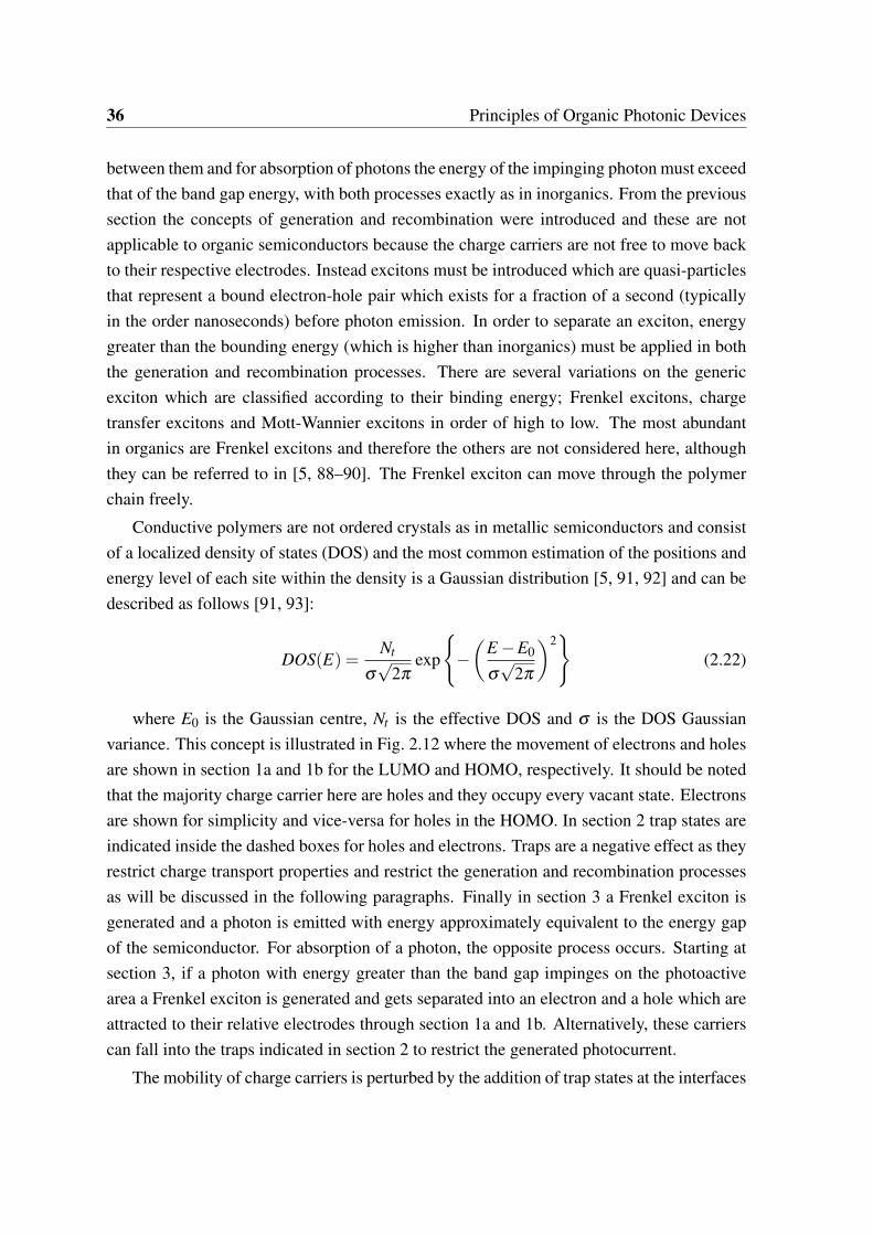
36 Principles of Organic Photonic Devices
between them and for absorption of photons the energy of the impinging photon must exceedthat of the band gap energy, with both processes exactly as in inorganics. From the previoussection the concepts of generation and recombination were introduced and these are notapplicable to organic semiconductors because the charge carriers are not free to move backto their respective electrodes. Instead excitons must be introduced which are quasi-particlesthat represent a bound electron-hole pair which exists for a fraction of a second (typicallyin the order nanoseconds) before photon emission. In order to separate an exciton, energygreater than the bounding energy (which is higher than inorganics) must be applied in boththe generation and recombination processes. There are several variations on the genericexciton which are classified according to their binding energy; Frenkel excitons, chargetransfer excitons and Mott-Wannier excitons in order of high to low. The most abundantin organics are Frenkel excitons and therefore the others are not considered here, althoughthey can be referred to in [5, 88–90]. The Frenkel exciton can move through the polymerchain freely.
Conductive polymers are not ordered crystals as in metallic semiconductors and consistof a localized density of states (DOS) and the most common estimation of the positions andenergy level of each site within the density is a Gaussian distribution [5, 91, 92] and can bedescribed as follows [91, 93]:
DOS(E) =Nt
σ√
2πexp
−(
E −E0
σ√
2π
)2
(2.22)
where E0 is the Gaussian centre, Nt is the effective DOS and σ is the DOS Gaussianvariance. This concept is illustrated in Fig. 2.12 where the movement of electrons and holesare shown in section 1a and 1b for the LUMO and HOMO, respectively. It should be notedthat the majority charge carrier here are holes and they occupy every vacant state. Electronsare shown for simplicity and vice-versa for holes in the HOMO. In section 2 trap states areindicated inside the dashed boxes for holes and electrons. Traps are a negative effect as theyrestrict charge transport properties and restrict the generation and recombination processesas will be discussed in the following paragraphs. Finally in section 3 a Frenkel exciton isgenerated and a photon is emitted with energy approximately equivalent to the energy gapof the semiconductor. For absorption of a photon, the opposite process occurs. Starting atsection 3, if a photon with energy greater than the band gap impinges on the photoactivearea a Frenkel exciton is generated and gets separated into an electron and a hole which areattracted to their relative electrodes through section 1a and 1b. Alternatively, these carrierscan fall into the traps indicated in section 2 to restrict the generated photocurrent.
The mobility of charge carriers is perturbed by the addition of trap states at the interfaces
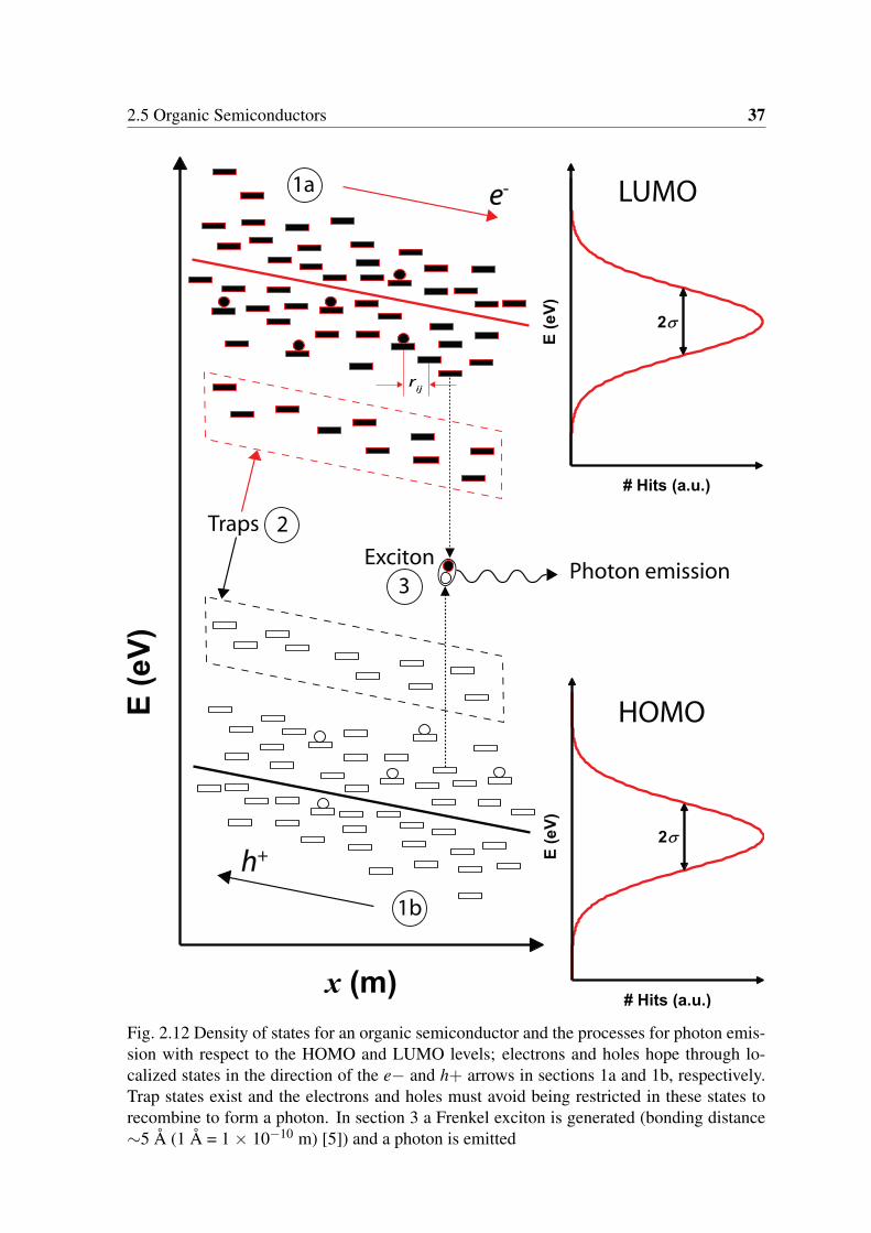
2.5 Organic Semiconductors 37
rij
e-
h+
LUMO
HOMO
Traps
ExcitonPhoton emission
1a
1b
3
2
Fig. 2.12 Density of states for an organic semiconductor and the processes for photon emis-sion with respect to the HOMO and LUMO levels; electrons and holes hope through lo-calized states in the direction of the e− and h+ arrows in sections 1a and 1b, respectively.Trap states exist and the electrons and holes must avoid being restricted in these states torecombine to form a photon. In section 3 a Frenkel exciton is generated (bonding distance∼5 Å (1 Å = 1 × 10⁻¹⁰ m) [5]) and a photon is emitted
38 Principles of Organic Photonic Devices
(intrinsic traps) and due to defects in the layers and production processes (extrinsic traps).Both types of trap impede transport properties of organics as they interfere with the recom-bination and generation processes by introducing new energy levels that have energy levelsbetween the HOMO and LUMO levels meaning charge carriers must drop into the traps asthey propagate across the device [94], refer to Fig. 2.12. Clearly if a charge carrier is con-fined inside a trap, it cannot assist with the overall generation of photons or photocurrent.Besides organic photonic devices, traps are also known to cause a shift in turn-on thresholdvoltage in organic field effect transistors (OFETs) [94]. The issue of trapping is one of thekey challenges facing physical chemists who are researching organics.
Charge carriers (and therefore current flow) can be considered to be ‘hopping’ fromstate to state in the localized densities previously mentioned. The hopping rate υi j betweenlocalized states i and j is known as the Miller-Abrahams rate [95]:
υi j = υ0 exp(−2γri j
)exp(
E j−EikBT
)if E j ≥ Ei
1 if E j ≤ Ei
(2.23)
where υ0 is a pre-factor, γ is the inverse localization length, ri j is the distance betweenlocalized states and E j −Ei is the energetic barrier that the charge carrier must overcome (asin Fig. 2.12).
2.6 The Bulk Heterojunction
In terms of PDs, in order to separate excitons into individual charge carriers, a larger energyis required than inorganics due to the high binding energy as mentioned in the previous sec-tion. To offer a solution to this problem, the concepts of electron donor and electron acceptormust be introduced. Electron donors have lower electron affinity (the difference between theband edge and the vacuum energy) than electron acceptors. It should be noted that a highelectron affinity is desirable for electron acceptors and vice-versa for electron donors. It ispossible to disassociate the exciton at the interface of an electron donor/acceptor configu-ration due to the unbalanced electron affinities (i.e. the unbalanced energy levels). In thisthesis only radiative decay of excitons is considered (non-radiative decay is also possibleas previous) and with the influence of an external voltage the generated electrons and holesare attracted to their respective electrodes. The bulk heterojunction (BHJ) is an interpene-trated blend of electron donor and electron acceptor that provides such an interface that isdistributed across the entire photoactive area of the organic photonic device as illustrated inFig. 2.13. The reason for interpenetration is due to the fact that radiative decay of excitons

2.6 The Bulk Heterojunction 39
depends on the distance of exciton generation from the electron acceptor-electron donorborder (for distances > 10 nm the exciton will not offer radiative decay [5]). BHJs werefirst introduced in [96] and are popular in OPVs and OPDs due to the fact that they aresoluble and provide extremely low cost processing [54].
Cathode
Anode
O H
O
CH 3
S
C H 3
S
C H 3
S
CH 3
S
C H 3
SCH 3 C H 3
n
Electron donor
Electron acceptor
hv+
-
Fig. 2.13 The bulk heterojunction concept made up of electron acceptor and electron donorincluding electron acceptor and electron donor materials, PCBM and P3HT, respectively
As illustrated in 2.13 the materials selected for electron acceptor and electron donorare [6,6]-phenyl-C61-butyric acid methyl ester (PCBM) and P3HT, respectively. PCBMis a Buckminsterfullerene derivative (the 1996 Nobel Prize in Chemistry was awarded forthe discovery of Buckminsterfullerene) that offers the advantage of having high electronaffinity to produce efficient electron transfer. PCBM is also soluble. P3HT is a conductivepolymer (the 2000 Nobel Prize in Chemistry was awarded for its discovery) consisting ofπ–conjugated orbitals which are advantageous for photoactive devices. In this thesis, theOPDs are based on the BHJ principle and are manufactured by Siemens AG, CorporateTechnology. Top and bottom view photographs of the OPD are provided in Fig. 2.14 and2.15, respectively.
The bottom view features most of the features that are important to the OPD and adigitally produced model of the OPD highlights these key aspects in Fig. 2.16.
The OPDs share the aluminium electrode (the cathode) and have an individually struc-tured anode that allows each diode to read out an independent data stream. The anode ismade from indium tin oxide (ITO) which is a transparent conductive metal. The fact that

40 Principles of Organic Photonic Devices
Fig. 2.14 Top view of the OPD used in this thesis
Fig. 2.15 Bottom view of the OPD used in this thesis (four 1 cm2 diodes)
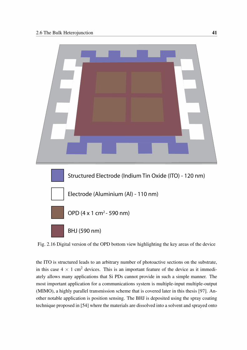
2.6 The Bulk Heterojunction 41
Structured Electrode (Indium Tin Oxide (ITO) - 120 nm)
Electrode (Aluminium (Al) - 110 nm)
OPD (4 x 1 cm2 - 590 nm)
BHJ (590 nm)
Fig. 2.16 Digital version of the OPD bottom view highlighting the key areas of the device
the ITO is structured leads to an arbitrary number of photoactive sections on the substrate,in this case 4 × 1 cm2 devices. This is an important feature of the device as it immedi-ately allows many applications that Si PDs cannot provide in such a simple manner. Themost important application for a communications system is multiple-input multiple-output(MIMO), a highly parallel transmission scheme that is covered later in this thesis [97]. An-other notable application is position sensing. The BHJ is deposited using the spray coatingtechnique proposed in [54] where the materials are dissolved into a solvent and sprayed onto
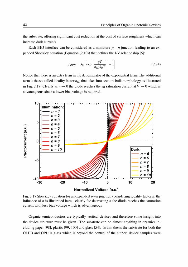
42 Principles of Organic Photonic Devices
the substrate, offering significant cost reduction at the cost of surface roughness which canincrease dark currents.
Each BHJ interface can be considered as a miniature p – n junction leading to an ex-panded Shockley equation (Equation (2.10)) that defines the I-V relationship [5]:
JMPN = J0
[exp[
qVnIDkBT
]−1]
(2.24)
Notice that there is an extra term in the denominator of the exponential term. The additionalterm is the so-called ideality factor nID that takes into account bulk morphology as illustratedin Fig. 2.17. Clearly as n → 0 the diode reaches the J0 saturation current at V → 0 which isadvantageous since a lower bias voltage is required.
-10
-5
0
5
10
Ph
oto
cu
rre
nt
(a.u
.)
-30 -20 -10 0 10 20
Normalized Voltage (a.u.)
Illumination: n = 1 n = 2 n = 3 n = 4 n = 5 n = 6 n = 7 n = 8 n = 9 n = 10 Dark:
n = 5 n = 6 n = 7 n = 8 n = 9 n = 10
Fig. 2.17 Shockley equation for an expanded p – n junction considering ideality factor n; theinfluence of n is illustrated here - clearly for decreasing n the diode reaches the saturationcurrent with less bias voltage which is advantageous
Organic semiconductors are typically vertical devices and therefore some insight intothe device structure must be given. The substrate can be almost anything in organics in-cluding paper [98], plastic [99, 100] and glass [54]. In this thesis the substrate for both theOLED and OPD is glass which is beyond the control of the author; device samples were

2.7 Summary 43
received from project partners and hence the material stacks are presumed to be optimizedon the glass substrate. It would be extremely interesting to perform measurements with aflexible device in order to examine the effects on the communications performance underdifferent flex stresses. The anode is generally made from transparent ITO although there is agrowing argument for using graphene due to the emergence of high efficiency devices withgraphene anodes [101]. The next layers are the organic layers. In state-of-the-art OLEDdevices the organic layers are made up of (from bottom to top) a hole injection layer, a holetransport layer, an emissive layer, an electron transport layer, an electron injection layerfollowed by the cathode which is generally aluminium since it is cheap and not necessaryto be transparent. There are many devices that offer an increase in performance at the costof increased complexity such as multiple photon emitters that are not covered here but arereferred to in [71]. In BHJ OPDs the stack structure is significantly less complex; requiringonly the two electrodes, the BHJ and an optional interlayer; selected as P3HT in this thesisbecause it offers the highest bandwidth [61]. The interlayer is not covered here, howeverit can have a profound effect on the performance of critical parameters of the device suchas bandwidth; for a detailed analysis, refer to [61]. As mentioned, the BHJ is an interpene-trated blend of P3HT:PCBM which are extremely popular materials in BHJ devices due totheir relatively high efficiency and solubility. The band gap energy of P3HT:PCBM is ∼ 2eV which is ideal for VLC applications as the cut-off wavelength is ∼ 650 nm which cuts aportion of the red wavelengths that would possibly be useful for WDM. By introducing a fur-ther, low band gap material into the BHJ blend such as poly[2,6-(4,4-bis-(2-ethylhexyl)-4H-cyclopenta[2,1-b;3,4-b’]dithiphene)-alt-4,7-(2,1,3-benzothiadiazole)] (PCPDTBT) the BHJband gap can be reduced so the absorption spectrum extends into the NIR region and allowsthe absorption of such wavelengths. The working principles of P3HT:PCBM and similarBHJs are well covered in literature and the reader is encouraged to refer to [5, 54, 96] sinceno details are given here.
2.7 Summary
In this chapter, the prerequisite theoretical knowledge for organic semiconductors is out-lined, starting with the essential band theory from inorganic semiconductors, including thegeneration and absorption of photons. This is subsequently related to the dislocated cloudsof charge carriers that exist in organic semiconductors due to the linear combination of or-bitals. The HOMO and LUMO energy levels are introduced and are related to inorganicsfor the readers understanding. Finally details of the OPDs used in this work are provided.


Chapter 3
Principles of Visible LightCommunications
3.1 Introduction
In this chapter the basic theory of VLC is outlined plus the theory of the modulationschemes. There are a number of possible link configurations as illustrated in Fig. 3.1. Firstlythere is the directed line-of-sight (LOS) method where the LED is pointed directly at thereceiver with no offset in order to maximize SNR and hence increase the data rate untilthere the bandwidth limitations are met. Another LOS configuration is the non-directed linkwhich essentially provides the system with mobility and aims to flood the receiving planewith optical power. There are also some non-LOS (NLOS) configurations shown wherethe link relies on reflections from the walls and ceiling to receive the data. The differencebetween the directed and non-direct configurations is just the focusing of the beam; thatis to say that the directed NLOS method requires either beam tracking or no mobility inorder to recover the data and the non-directed NLOS configuration (often called diffuse)does not care about the position of the PD on the receiving plane. This thesis focuses on thedirected LOS topology since it offers the highest SNR and is the most popular VLC topol-ogy. Further, as was shown in the previous chapter the bandwidth of the OPD is directlyproportional to the incident light density and it is desirable to maximize this constraint inorder to maximize the system capacity.
The block diagram of a typical VLC system is shown in Fig. 3.2. A pseudorandombinary sequence (PRBS) xi is generated either by MATLAB or by a field programmablegate array (FPGA) using shift registers. The data must then be formatted into an appropriatemodulation scheme di, generally non-return-to-zero OOK and Lth order PPM are used in
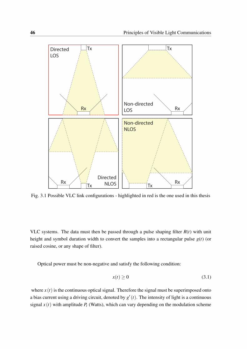
46 Principles of Visible Light Communications
Tx Tx
Tx Tx
Rx Rx
Rx Rx
Directed
LOS
Non-directed
LOS
Directed
NLOS
Non-directed
NLOS
Fig. 3.1 Possible VLC link configurations - highlighted in red is the one used in this thesis
VLC systems. The data must then be passed through a pulse shaping filter R(t) with unitheight and symbol duration width to convert the samples into a rectangular pulse g(t) (orraised cosine, or any shape of filter).
Optical power must be non-negative and satisfy the following condition:
x(t)≥ 0 (3.1)
where x(t) is the continuous optical signal. Therefore the signal must be superimposed ontoa bias current using a driving circuit, denoted by g′ (t). The intensity of light is a continuoussignal x(t) with amplitude Pt (Watts), which can vary depending on the modulation scheme
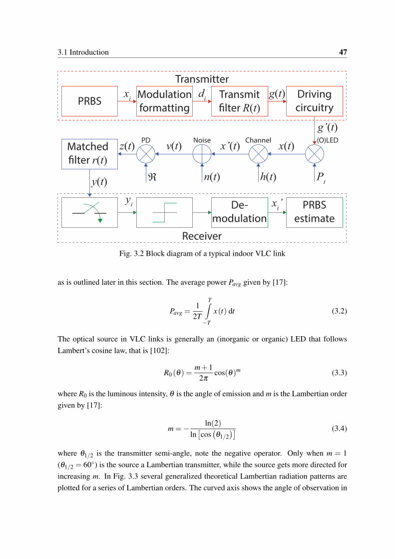
3.1 Introduction 47
PRBSModulation
formatting
Transmit
lter R(t)
Driving
circuitry
(O)LEDChannelNoisePDMatched
lter r(t)
Receiver
De-
modulation
PRBS
estimate
Pt
h(t)n(t)ℜ
Transmitter
xi
di
g(t)
g’(t)
x(t)x’(t)v(t)z(t)
y(t)
yi x
i’
Fig. 3.2 Block diagram of a typical indoor VLC link
as is outlined later in this section. The average power Pavg given by [17]:
Pavg =1
2T
T∫−T
x(t) dt (3.2)
The optical source in VLC links is generally an (inorganic or organic) LED that followsLambert’s cosine law, that is [102]:
R0 (θ) =m+1
2πcos(θ)m (3.3)
where R0 is the luminous intensity, θ is the angle of emission and m is the Lambertian ordergiven by [17]:
m =− ln(2)ln[cos(θ1/2
)] (3.4)
where θ1/2 is the transmitter semi-angle, note the negative operator. Only when m = 1(θ1/2 = 60) is the source a Lambertian transmitter, while the source gets more directed forincreasing m. In Fig. 3.3 several generalized theoretical Lambertian radiation patterns areplotted for a series of Lambertian orders. The curved axis shows the angle of observation in

48 Principles of Visible Light Communications
degrees while the flat axis is the normalized emission intensity. Lambertian emitters (m = 1)have the same perceived intensity at any observation angle, unlike any other value for m. Itis assumed that m = 1 for WPLEDs and OLEDs as has widely been reported [103, 104].
0 0.2 0.4 0.6 0.8 1-90
-80
-70
-60
-50
-40
-30-20
-10 0 1020
30
40
50
60
70
80
90
Angle (°)
Normalized Emission Power
m = 0.1 m = 0.5 m = 1.0 m = 2.0 m = 3.0 m = 4.0 m = 5.0
Fig. 3.3 Lambertian emission profiles of several Lambertian orders
In order to maximize the luminous intensity it is necessary to set θ = 0 and thus directedLOS link will provide the best signal quality. While it is possible to use external modulationmethods such as a Mach-Zander modulator (MZM) in fibre optic links, to date VLC hasexclusively used intensity modulation, where the electrical signal amplitude is reflected inthe intensity of the optical power. Each device has a transfer function known as the L–Icurve, where L is the optical power and I is the drive current) and an example of intensitymodulation is illustrated in Fig. 3.4. The operating point is selected due to its linearity. Eachdevice has a pseudo-linear and safe operating region where extended operation can occur.If the drive current is pushed into the roll-over region or beyond signal distortion can occurin conjunction with significant device degradation. Next, the indoor channel h(t) must betaken into account. The intensity of the optical power transmitted over the channel drops bya factor of 1/d2, where d is the distance to the receiving plane.

3.1 Introduction 49
1.0
0.8
0.6
0.4
0.2
0.0
No
rma
lize
d O
pti
ca
l P
ow
er
(a.u
.)
43210
Drive Current (A)
SignalBias Current
Optical Source Example
Fig. 3.4 Example L-I curve for intensity modulation of an optical source
The channel can be described either in terms of the impulse or frequency response, i.e.:
H ( f ) =∞∫
−∞
h(t)e−2π f t dt (3.5)
The frequency response is the most popular choice, as the channel H ( f ) represents a DCgain less than unity [17, 26]:
H (0) =Ar
d2 R0 (θ)cos(ϕ) (3.6)
where Ar is the photoactive area of the PD and ϕ is the angle of incidence to the PD.
50 Principles of Visible Light Communications
The main source of noise n(t) in VLC links is shot noise which is independent of anduncorrelated to the signal. IR and thermal noise also contribute but they are considerednegligible in comparison to the shot noise. The additive white Gaussian noise (AWGN)model can be adopted with single sided power spectral density N0 [17, 105]:
N0 = 2qID (3.7)
where q is the charge of an electron and ID is the PD dark current. The noise and channelperturbed signal, v(t) = x(t)⊗ h(t) + n(t), (refer to Fig. 3.2) is detected by a PD withresponsivity ℜ which is less than unity for PIN PD.
The received optical power Pr impinging on the PD is given by:
Pr = H (0)Pt (3.8)
Clearly neither the wavelength nor the signal frequency influences the average received opti-cal power and there are no non-linear affects for the wavelengths and frequencies concerned.It is not clear where this assumption breaks down and non-linear effects occur because ingeneral the bandwidths of the components are significantly lower than the channel. The pho-tocurrent denoted z(t) is generally converted into a voltage by a transimpedance amplifier(TIA) which is not shown in Fig. 3.2. The SNR at the receiver is given by [17, 105]:
SNR =(ℜPr)
2
RbN0=
ℜ2H (0)2 P2t
RbN0(3.9)
It is well known that PDs are square law detectors, hence the square term. It is clear that theSNR is a function of the transmission speed. A higher transmission speed causes a reductionin SNR due to an enhancement of noise [17]. The reason for this is due to the additionalbandwidth requirement causing a higher susceptibility to noise.
Typically a matched filter r (t) is used in order to maximize the SNR at the receiver.The matched filter can only be used when the pulse shape is known at the receiver, i.e. inOOK and L-PPM links. The matched filter is simply a tool to ensure that the signal is atits maximum amplitude at the sampling instance and aims to undo the dispersion caused bythe channel or bandwidth limitations. There are numerous methods including the use of theautocorrelation function, a transversal linear filter or the ‘integrate and dump’ method [106],which is the most simple and is outlined here. For the mathematical proof of the matchedfilter, refer to [106, 107].
The signal SNR is defined by the level of received power in comparison to the levelof AWGN noise. The integrate and dump is a special case of the matched filter which

3.1 Introduction 51
improves the SNR by performing the cumulative sum of the amplitude over the bit period,then returning to zero and repeating for the next symbol period. Therefore the amplitude atthe output of the filter at end of the symbol period is much larger than the amplitude at anypoint before the filter, as can be seen in Fig. 3.5. The decision on the symbol can be madeusing a sampler that samples at the rate of the symbol duration when the amplitude is at itspeak as indicated by the dashed line. Subsequently an average level threshold can be usedto decide the absolute level of the bits.
-1.0
-0.5
0.0
0.5
1.0
Am
pli
tud
e (
a.u
.)
0 Tb 2Tb 3Tb 4Tb 5Tb 6Tb 7Tb 8Tb 9Tb 10Tb
Time (s)
-1.0
-0.5
0.0
0.5
1.0
Am
pli
tud
e (
a.u
.)
-5.0
-2.5
0.0
2.5
5.0
Am
pli
tud
e (
a.u
.)
Fig. 3.5 Operation of matched filter; the data (top) is perturbed by noise (middle) and theoutput of the matched filter (bottom) is much larger in magnitude in comparison to the noiselevel than the noisy signal (note the y-axis magnitude), which is reflected in an increasedSNR
The data is then de-mapped from the modulation format and the BER performance is

52 Principles of Visible Light Communications
measured, either by Q-factor or by exact comparisons between transmitted and receiveddata. Typically in VLC, BER = 10−6 is deemed sufficient [59]. Q-factor is given by:
Q =υH −υL
σH +σL(3.10)
where υH and υL are the mean received voltages and σH and σL are the standard deviationsof the 1-level and 0-level signals before being sliced, respectively. There are a number ofmodulation schemes in common use for VLC systems; the most popular are M-PAM andL-PPM. M-PAM offers unrivalled bandwidth efficiency while L-PPM is the most powerefficient scheme. A block diagram for each modulation scheme is also presented with thevarious receiver topologies. The mathematical theory of each of the modulation schemes iscovered here in order to understand their bandwidth, power requirements and probability oferror performance and thus their suitability for future OVLC links.
3.2 Modulation Schemes
The reason no further modulation schemes other than M-PAM and L-PPM are selected isbecause of their bandwidth and power requirement characteristics, respectively. PAM isthe most bandwidth digital modulation scheme (aside from QAM) while PPM is the mostpower efficient. This is reflected in Fig. 3.6 which shows the spectral efficiency of a numberof modulation schemes at a BER target of 10−6 including phase shift keying (PSK) andfrequency shift keying (FSK) which have characteristics closest to those of the modulationschemes under test. Every other digital modulation scheme offers performance somewherebetween PAM and PPM so are not tested in this thesis. M-PAM/QAM approaches thecapacity limit as M →∞ while L-PPM approaches the power limit under the same condition.
By far the most popular modulation scheme is OOK due to the simplicity of implemen-tation and bandwidth efficiency [58]. OOK is the lowest order of M-ary pulse amplitudemodulation where the order of modulation is M = 2k for k > 0. OOK is based on two levelsso M = 2.
3.2.1 M-ary Pulse Amplitude Modulation
The intensity of the optical power is made proportional to the amplitude of the electricalcurrent. Therefore in the case of unipolar OOK, in order to transmit a binary 1-level a pulseof energy is transmitted over the symbol period Tb. To transmit a binary 0-level there is an
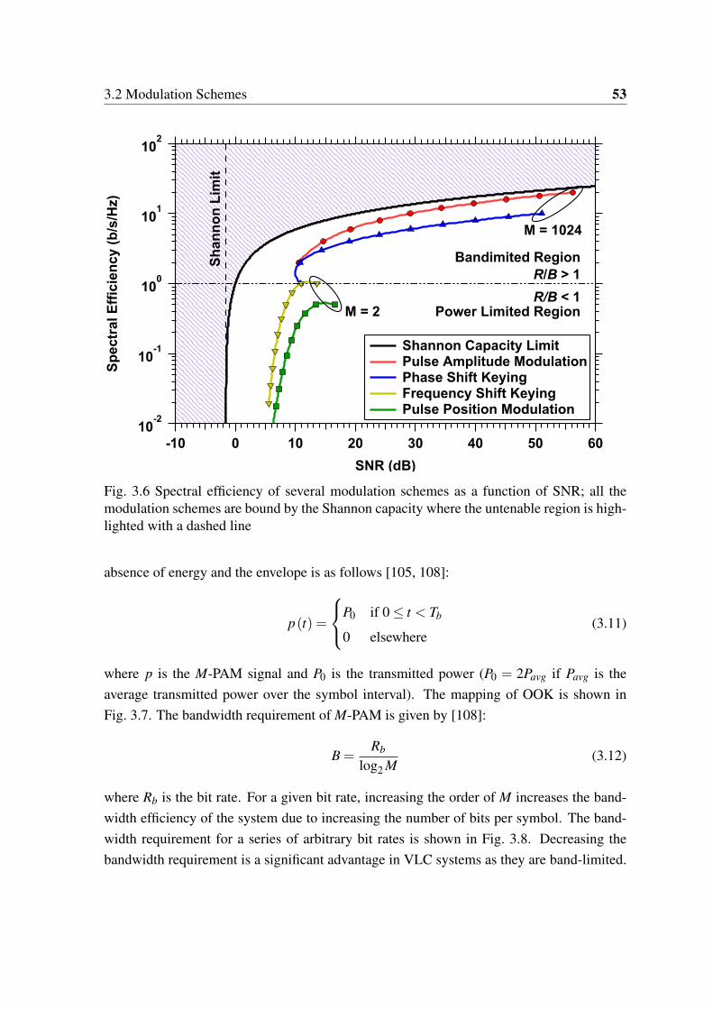
3.2 Modulation Schemes 53
10-2
10-1
100
101
102
Sp
ec
tra
l E
ffic
ien
cy
(b
/s/H
z)
6050403020100-10
SNR (dB)
R/B > 1
R/B < 1
M = 1024
Power Limited Region
Bandimited Region
M = 2
Sh
an
no
n L
imit
Shannon Capacity Limit Pulse Amplitude Modulation Phase Shift Keying Frequency Shift Keying Pulse Position Modulation
Fig. 3.6 Spectral efficiency of several modulation schemes as a function of SNR; all themodulation schemes are bound by the Shannon capacity where the untenable region is high-lighted with a dashed line
absence of energy and the envelope is as follows [105, 108]:
p(t) =
P0 if 0 ≤ t < Tb
0 elsewhere(3.11)
where p is the M-PAM signal and P0 is the transmitted power (P0 = 2Pavg if Pavg is theaverage transmitted power over the symbol interval). The mapping of OOK is shown inFig. 3.7. The bandwidth requirement of M-PAM is given by [108]:
B =Rb
log2 M(3.12)
where Rb is the bit rate. For a given bit rate, increasing the order of M increases the band-width efficiency of the system due to increasing the number of bits per symbol. The band-width requirement for a series of arbitrary bit rates is shown in Fig. 3.8. Decreasing thebandwidth requirement is a significant advantage in VLC systems as they are band-limited.

54 Principles of Visible Light Communications
0
P0
x(t
)
0 Tbt
0
P0
x(t
)
0 Tbt
Pavg
NRZ OOK 1-level NRZ OOK 0-level
Fig. 3.7 Transmitted waveforms for NRZ-OOK for the 1- and 0-levels
10
8
6
4
2
0
Ban
dw
idth
Req
uir
em
en
t (H
z)
54321
log2(M) (bit/sym)
10987654321
Data Rate (b/s)
Fig. 3.8 Bandwidth efficiency of M-PAM, recalling that 2-PAM is OOK

3.2 Modulation Schemes 55
The power spectral densities (PSDs) P( f ) of M-PAM are given by [105, 106]:
P( f ) = (Pavgℜ)2 Tb
(sin(π f Tb)
π f Tb
)2
[1+Rbδ ( f )] (3.13)
recalling that ℜ is the PD responsivity, f is the frequency and δ ( f ) is the Dirac delta func-tion. The PSDs of several orders of M-PAM are plotted in Fig. 3.9. The x-axis (frequency)
4
3
2
1
0
Po
we
r S
pe
ctr
al
De
ns
ity
(a
.u.)
1.21.00.80.60.40.20.0
Frequency (a.u.)
Tb(OOK)Tb(4-PAM)Tb(8-PAM)
PSD: M = 2 M = 4 M = 8
Fig. 3.9 Power spectral densities of M-PAM with box axes normalized to OOK
is normalized to an OOK bit rate of 1 arbitrary unit for M = 2 and the y-axis (PSD) isalso normalized to OOK. Therefore it is clear that as the order of M increases, the powerrequirement also increases while the required symbol period a decrease, assuming that thetransmission speed is the same and the distance between symbols is also equal in each case.Also noteworthy from Fig. 3.9 is there are significant spectral contributions around the DCand low frequency regions which can introduce the baseline wander phenomenon (that isdescribed later in this Chapter) and make threshold detection impossible [41].
A system block diagram for M-PAM is shown in Fig. 3.10. The NRZ coded PRBS dataxi is passed through a rectangular unit-amplitude pulse shaping filter with a symbol periodimpulse response in order to produce a continuous signal. The output of the transmit filter
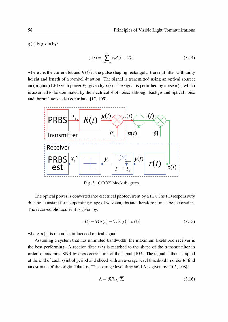
56 Principles of Visible Light Communications
g(t) is given by:
g(t) =∞
∑i=−∞
xiR(t − iTb) (3.14)
where i is the current bit and R(t) is the pulse shaping rectangular transmit filter with unityheight and length of a symbol duration. The signal is transmitted using an optical source;an (organic) LED with power P0, given by x(t). The signal is perturbed by noise n(t) whichis assumed to be dominated by the electrical shot noise; although background optical noiseand thermal noise also contribute [17, 105].
PRBS R(t)
ℜn(t)
g(t)
yi
xi’
r(t)t = ts
PRBSest
P0
xi
x(t) v(t)
z(t)
y(t)
Transmitter
Receiver
Fig. 3.10 OOK block diagram
The optical power is converted into electrical photocurrent by a PD. The PD responsivityℜ is not constant for its operating range of wavelengths and therefore it must be factored in.The received photocurrent is given by:
z(t) = ℜυ (t) = ℜ [x(t)+n(t)] (3.15)
where υ (t) is the noise influenced optical signal.Assuming a system that has unlimited bandwidth, the maximum likelihood receiver is
the best performing. A receive filter r (t) is matched to the shape of the transmit filter inorder to maximize SNR by cross correlation of the signal [109]. The signal is then sampledat the end of each symbol period and sliced with an average level threshold in order to findan estimate of the original data x′i. The average level threshold Λ is given by [105, 108]:
Λ = ℜP0√
Tb (3.16)
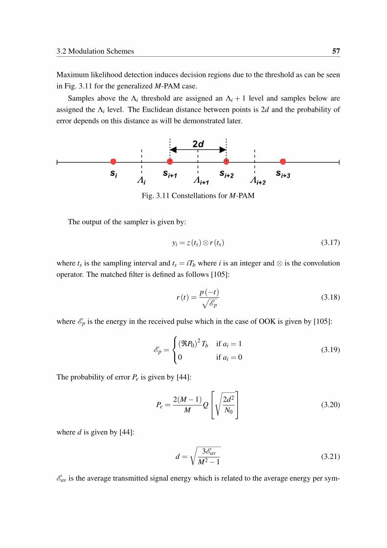
3.2 Modulation Schemes 57
Maximum likelihood detection induces decision regions due to the threshold as can be seenin Fig. 3.11 for the generalized M-PAM case.
Samples above the Λi threshold are assigned an Λi + 1 level and samples below areassigned the Λi level. The Euclidean distance between points is 2d and the probability oferror depends on this distance as will be demonstrated later.
Fig. 3.11 Constellations for M-PAM
The output of the sampler is given by:
yi = z(ts)⊗ r (ts) (3.17)
where ts is the sampling interval and ts = iTb where i is an integer and ⊗ is the convolutionoperator. The matched filter is defined as follows [105]:
r (t) =p(−t)√
Ep(3.18)
where Ep is the energy in the received pulse which in the case of OOK is given by [105]:
Ep =
(ℜP0)2 Tb if ai = 1
0 if ai = 0(3.19)
The probability of error Pe is given by [44]:
Pe =2(M−1)
MQ
√2d2
N0
(3.20)
where d is given by [44]:
d =
√3Eav
M2 −1(3.21)
Eav is the average transmitted signal energy which is related to the average energy per sym-
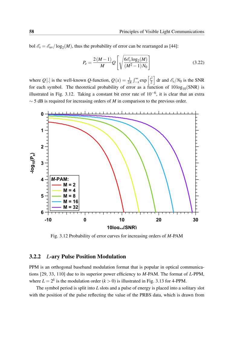
58 Principles of Visible Light Communications
bol Es = Eav/ log2(M), thus the probability of error can be rearranged as [44]:
Pe =2(M−1)
MQ
[√6Es log2(M)
(M2 −1)N0
](3.22)
where Q [.] is the well-known Q-function, Q(x) = 12π
∫∞
−x exp[
t2
2
]dt and Es/N0 is the SNR
for each symbol. The theoretical probability of error as a function of 10log10(SNR) isillustrated in Fig. 3.12. Taking a constant bit error rate of 10−6, it is clear that an extra∼ 5 dB is required for increasing orders of M in comparison to the previous order.
6
5
4
3
2
1
0
-lo
g10(P
e)
3020100-10
10log10(SNR)
M-PAM: M = 2 M = 4 M = 8 M = 16 M = 32
Fig. 3.12 Probability of error curves for increasing orders of M-PAM
3.2.2 L-ary Pulse Position Modulation
PPM is an orthogonal baseband modulation format that is popular in optical communica-tions [29, 33, 110] due to its superior power efficiency to M-PAM. The format of L-PPM,where L = 2k is the modulation order (k > 0) is illustrated in Fig. 3.13 for 4-PPM.
The symbol period is split into L slots and a pulse of energy is placed into a solitary slotwith the position of the pulse reflecting the value of the PRBS data, which is drawn from

3.2 Modulation Schemes 59
the set i = 0, . . . ,L˘1. The rest of the slots are left empty. The slot duration TL is found asfollows [105]:
TL = TbiL
(3.23)
The L-PPM envelope is given by [111]:
s(t) =
1 if (i−1)TL ≤ t < kTL
0 elsewhere(3.24)
The L-PPM signal x(t) is therefore given by [111]:
x(t) = LP0
L−1
∑l
ClR(t − lTL) (3.25)
where the L-PPM code word Cl = [C0, C1, . . . , CL−1].
OO
K
Time (a.u.)
4-P
PM
TS TL
0 1 1 0 1 1 0 0 1 0 0 1
1 2 3 0 2 1
Data
Fig. 3.13 Raw data code into the 4-PPM format with a comparison to OOK
The pulse shaping function R(t) once more has unity height and duration TL and LPavg
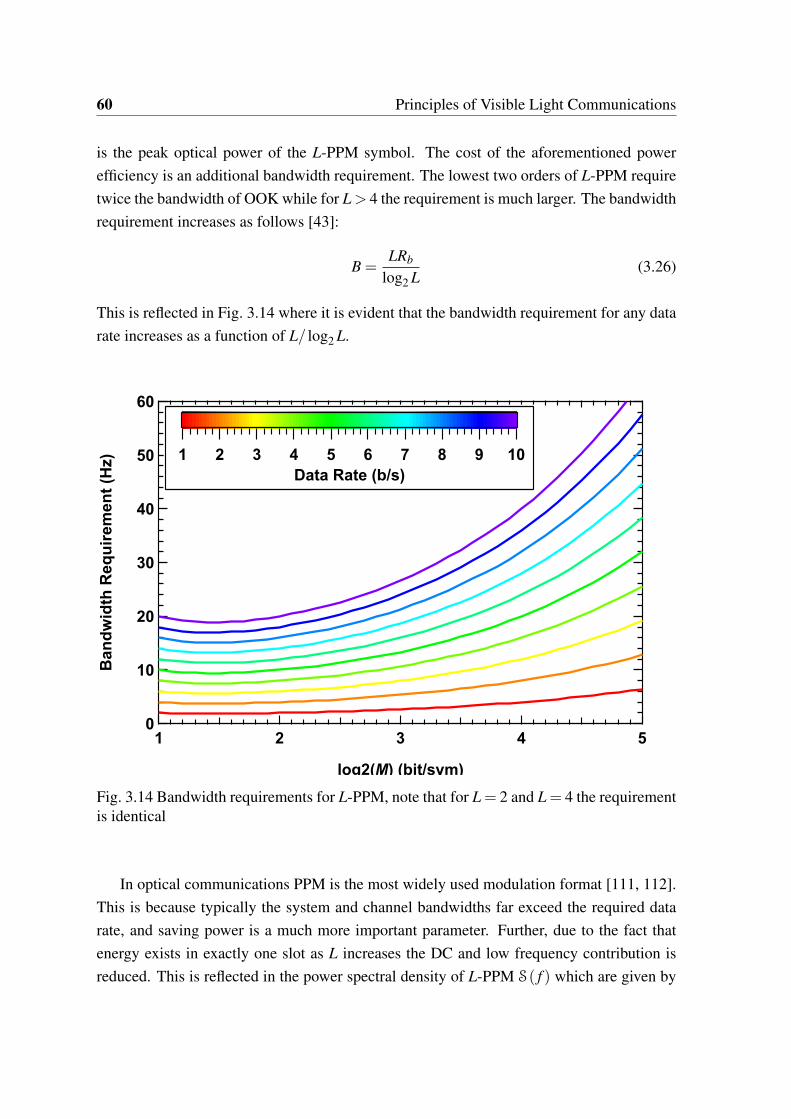
60 Principles of Visible Light Communications
is the peak optical power of the L-PPM symbol. The cost of the aforementioned powerefficiency is an additional bandwidth requirement. The lowest two orders of L-PPM requiretwice the bandwidth of OOK while for L > 4 the requirement is much larger. The bandwidthrequirement increases as follows [43]:
B =LRb
log2 L(3.26)
This is reflected in Fig. 3.14 where it is evident that the bandwidth requirement for any datarate increases as a function of L/ log2 L.
60
50
40
30
20
10
0
Ba
nd
wid
th R
eq
uir
em
en
t (H
z)
54321
log2(M) (bit/sym)
10987654321
Data Rate (b/s)
Fig. 3.14 Bandwidth requirements for L-PPM, note that for L = 2 and L = 4 the requirementis identical
In optical communications PPM is the most widely used modulation format [111, 112].This is because typically the system and channel bandwidths far exceed the required datarate, and saving power is a much more important parameter. Further, due to the fact thatenergy exists in exactly one slot as L increases the DC and low frequency contribution isreduced. This is reflected in the power spectral density of L-PPM S( f ) which are given by

3.2 Modulation Schemes 61
[111]:
S( f ) = |R|2 [Sc ( f )+Sd ( f )] (3.27)
where R( f ) is the Fourier transform of the pulse shape and Sc ( f ) and Sd ( f ) are as follows[111]:
Sc ( f ) =1
LTL
[(1− 1
L
)+
2L
L−1
∑l
(lL−1)
cos(2π f lTL)
](3.28)
Sd ( f ) =2π
(LTL)2
∞
∑l=−∞
δ
(f − l
TL
)(3.29)
The bit rate is 1 arbitrary unit. It is clear that the bandwidth requirements increase as theorder of L increases. Also it is important to notice that the spectral components aroundDC and the low frequencies are insignificant in comparison to M-PAM. This has severaladvantages including protection from baseline wander and artificial light interference due tohigh pass filtering [40, 41]. The PSDs are illustrated in Fig. 3.15.
3.0
2.5
2.0
1.5
1.0
0.5
0.0
Po
wer
Sp
ectr
al D
en
sit
y (
a.u
.)
543210
Frequency (a.u.)
PSD: L = 2 L = 4 L = 8
Fig. 3.15 PSDs of L-PPM; note that 2-PPM and 4-PPM have the same bandwidth require-ment
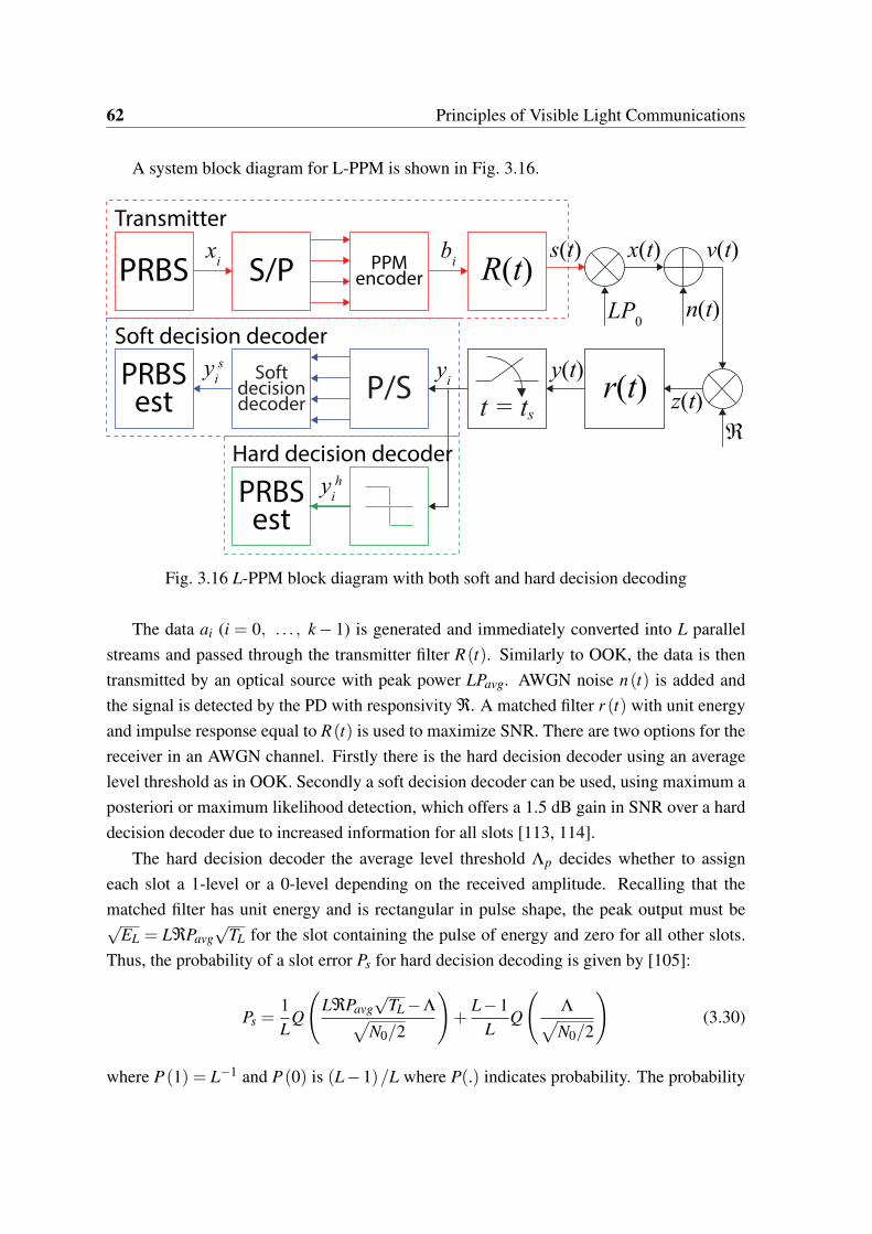
62 Principles of Visible Light Communications
A system block diagram for L-PPM is shown in Fig. 3.16.
PRBS R(t)
ℜ
n(t)
s(t)
yi
yis
r(t)t = ts
PRBSest
LP0
xi
x(t) v(t)
z(t)
y(t)
Transmitter
Soft decision decoder
S/PPPM
encoder
PRBSest
Softdecisiondecoder
P/S
Hard decision decoder
bi
yih
Fig. 3.16 L-PPM block diagram with both soft and hard decision decoding
The data ai (i = 0, . . . , k− 1) is generated and immediately converted into L parallelstreams and passed through the transmitter filter R(t). Similarly to OOK, the data is thentransmitted by an optical source with peak power LPavg. AWGN noise n(t) is added andthe signal is detected by the PD with responsivity ℜ. A matched filter r (t) with unit energyand impulse response equal to R(t) is used to maximize SNR. There are two options for thereceiver in an AWGN channel. Firstly there is the hard decision decoder using an averagelevel threshold as in OOK. Secondly a soft decision decoder can be used, using maximum aposteriori or maximum likelihood detection, which offers a 1.5 dB gain in SNR over a harddecision decoder due to increased information for all slots [113, 114].
The hard decision decoder the average level threshold Λp decides whether to assigneach slot a 1-level or a 0-level depending on the received amplitude. Recalling that thematched filter has unit energy and is rectangular in pulse shape, the peak output must be√
EL = LℜPavg√
TL for the slot containing the pulse of energy and zero for all other slots.Thus, the probability of a slot error Ps for hard decision decoding is given by [105]:
Ps =1L
Q
(LℜPavg
√TL −Λ√
N0/2
)+
L−1L
Q
(Λ√N0/2
)(3.30)
where P(1) = L−1 and P(0) is (L−1)/L where P(.) indicates probability. The probability

3.2 Modulation Schemes 63
of a pulse is generally far exceeded by that of the probability of an empty slot by a factorof L−1 so selecting Λ =
√EL/2 is not optimal but is a good approximation [105, 111]and
one that simplifies the slot error probability to [111]:
Ps = Q(√
EL
2N0
)(3.31)
This can be converted into the bit error probability in order to make a like-for-like compari-son with OOK as follows [111]:
Pe =
(L
2(L−1)
)− (1−Ps)
L (3.32)
The probability of a bit error is illustrated in Fig. 3.17. It is clear that for increasing ordersof L and a fixed probability of error (i.e. 10−6) the power requirement is required, whichis contrary to the M-PAM modulation format where the power requirement increases forhigher orders of M.
6
5
4
3
2
1
0
-lo
g10(P
e)
20151050-5-10
10log10(SNR)
L-PPM L = 2 L = 4 L = 8 L = 16 L = 32
Fig. 3.17 Probability of error curves for increasing orders of L-PPM
Soft decision decoding treats the PPM signal as a block code. The output of the matched
64 Principles of Visible Light Communications
filter is rearranged into an L-column matrix and selects the highest value as the 1-level andthe remaining values as a 0-level, removing the reliance on a threshold as follows [115]:
ys =
1 0 0 0
0 1 0 0
0 0 1 0
0 0 0 1
[yi yi+1 yi+2 yi+3
]=
yi
yi+1
yi+2
yi+3
(3.33)
Thus, a decision is made on which bit should be correctly assigned the 1-level. This methodhas been demonstrated to offer at least 1.5 dB gain in electrical SNR in non-directed LOSlinks such as the one implemented in this thesis.
3.2.3 Summary of Modulation Schemes
The modulation schemes used in this thesis, M-PAM and L-PPM have been outlined indetail and are summed up as follows. The key advantages are as follows: the bandwidthrequirement of M-PAM is lower than any other modulation scheme other than M-QAMwhich requires an imaginary channel. An imaginary channel is not possible in VLC andtherefore QAM cannot be implemented easily. Since OVLC systems are highly bandlimitedit is desirable to aim for a modulation scheme that can transmit more symbols per bit witha bandwidth that is as small as possible. The next closest modulation scheme is M-PSK;however the bandwidth requirement for PSK is twice that of PAM. Furthermore, PSK isa pass-band modulation while PAM is a baseband modulation which is more suitable forthe low-pass transfer functions exhibited in OVLC systems. The other modulation schemeunder test is L-PPM which is the most power efficient scheme. This is also importancedue to the electro-optic characteristics of OLEDs; i.e. commercial devices are not as ef-ficient as inorganic LEDs yet and thus the lower optical modulation index must be takeninto account. Therefore a power efficient modulation must be considered and there is nomodulation scheme more power efficient than L-PPM currently. M-FSK is similar to PSKin that it is a pass-band modulation scheme. However, the power requirement is twice thatof PPM. Therefore only PAM and PPM are considered in this thesis.
3.3 Equalization Theory
In this section the fundamental theory of equalizers is given. First equalization as an in-formation theory problem and potential solutions are outlined. Then a different view is
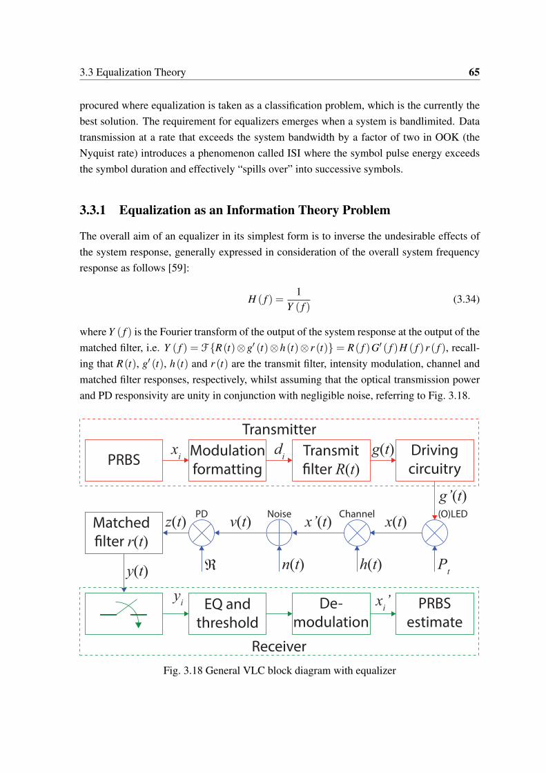
3.3 Equalization Theory 65
procured where equalization is taken as a classification problem, which is the currently thebest solution. The requirement for equalizers emerges when a system is bandlimited. Datatransmission at a rate that exceeds the system bandwidth by a factor of two in OOK (theNyquist rate) introduces a phenomenon called ISI where the symbol pulse energy exceedsthe symbol duration and effectively “spills over” into successive symbols.
3.3.1 Equalization as an Information Theory Problem
The overall aim of an equalizer in its simplest form is to inverse the undesirable effects ofthe system response, generally expressed in consideration of the overall system frequencyresponse as follows [59]:
H ( f ) =1
Y ( f )(3.34)
where Y ( f ) is the Fourier transform of the output of the system response at the output of thematched filter, i.e. Y ( f ) = FR(t)⊗g′ (t)⊗h(t)⊗ r (t) = R( f )G′ ( f )H ( f )r ( f ), recall-ing that R(t), g′ (t), h(t) and r (t) are the transmit filter, intensity modulation, channel andmatched filter responses, respectively, whilst assuming that the optical transmission powerand PD responsivity are unity in conjunction with negligible noise, referring to Fig. 3.18.
PRBSModulation
formatting
Transmit
lter R(t)
Driving
circuitry
(O)LEDChannelNoisePDMatched
lter r(t)
Receiver
De-
modulation
PRBS
estimate
Pt
h(t)n(t)ℜ
Transmitter
xi
di
g(t)
g’(t)
x(t)x’(t)v(t)z(t)
y(t)
yi x
i’EQ and
threshold
Fig. 3.18 General VLC block diagram with equalizer

66 Principles of Visible Light Communications
Equalizers are typically used to equalize the channel response which can be dispersiveor have fading properties in the outdoor environment. In this thesis the channel response isnot being equalized as it is independent of wavelength and frequency, see equations (3.5)–(3.5). Therefore H ( f ) is just a constant. The output of the matched filter can be listed asfollows [116]:
y(t) =∞
∑k=−∞
ak p(t − kTb)+n(t) (3.35)
where p(t) = R(t)⊗ g′ (t)⊗ h(t)⊗ r (t) and ak is the kth OOK symbol. Assuming y(t) isbeing sampled at a rate of ts = iTb then the output of the matched filter becomes [116]:
y(ts) =∞
∑k=−∞
ak p [(i− k)Tb]+n(ts) (3.36)
which can be expanded to [116]:
y(ts) = ai +∞
∑k=−∞
k =i
ak p [(i− k)Tb]+n(ts) (3.37)
where ai indicates the amplitude of the ith received symbol. The summand indicates thecontribution of ISI from the preceding and subsequent symbols to the system, and it istherefore possible to state that in order to achieve zero ISI, the following must be realised[116]:
p [(i− k)Tb] =
1 if i = k
0 if i = k(3.38)
which would mean that the receiver output would become [116]:
y(ts) = ai (3.39)
i.e. the system is not affected by ISI.
Considering the system response p(t), the factor that is deteriorating the overall systemresponse and introducing ISI is the low pass transfer functions of the organic devices aswas demonstrated in Chapter 2. Equalizing the low pass response will allow the data rateto be increased significantly in the presence of a high SNR. It should also be noted that theequalizers do not equalize the effects of noise.

3.3 Equalization Theory 67
The system response is found by pilot signal and careful filter design is required in orderto maximize the effectiveness of the equalizer. There are two main types of filter; analogueand digital. In the analogue domain a high pass filter RC equalizer is the only real choicewhile in the digital domain the zero forcing (ZF) and the decision feedback (DF) equalizersare the most popular. Both types have intrinsic advantages and disadvantages which aredocumented here.
3.3.2 RC Equalizer
An RC equalizer consists of a resistor and capacitor arranged into a high pass filter that isplaced between the data source and the optical source (pre equalizer), or the receiver andthe terminal (post equalizer). The frequency response of the RC equalizer HRC ( f ) is givenby [39]:
HRC ( f ) = k−1 1+ j2π f τ
1+ j2π f τ
k
(3.40)
where k−1 = RL/(R+RL) is the DC co-efficient of the RC equalizer, R is the equalizerresistor value, RL is the load resistor (typically 50 Ω) and τ = RC is the RC time constant.The magnitude response is given by [39]:
|HRC ( f )|= k−1
√√√√ 1+4π2 f 2τ2
1+(
4π2 f 2τ2
k2
) (3.41)
In order to equalize the low pass frequency response, the high pass slope must be opposite,i.e. SL =−SH where SL and SH are the low and high pass filter slope responses, respectively,where SH is given by [39]:
SH =6πτ√
11−[2/k2]
(3.42)
Which leads to an approximate bandwidth B of [39]:
B ≤ 20log10 (k)SH
(3.43)
Clearly, the bandwidth is dependent on k. Selection of k decides the margin of equalizationfor the system; a high value of k allows for more equalization and vice-versa. There is arestriction on the selection of k, however, it cannot be increased indefinitely. The restriction

68 Principles of Visible Light Communications
is caused by the dynamic input range of the receiver ∆P = Pmax −Psense, where Pmax is thesaturation power of the receiver and Psense is the minimum power the receiver can sensecontrolled by the NEP. The restriction is given by [39]:
20 log10 (k)≤ ∆P (3.44)
The advantages of the RC equalizer are that it is extremely simple to implement and has beendemonstrated experimentally to offer a significant improvement in data rate in VLC systems[39], however as is shown in Chapter 2, the improvement is not as large as can be providedwith a classifying equalizer. The disadvantages are major. By introducing a high pass filter,there is an exponential power penalty that is introduced around the low frequencies. Thisis compounded by the fact that introducing that power penalty leads directly to the baselinewander effect due to the removal of the low frequencies.
The Baseline Wander Phenomena
BLW is a phenomenon whereby the signal randomly deviates from the DC level caused bythe attenuation of the low frequency components by a high pass filter or coupling capacitor.The shape of BLW is can be expressed as an exponentially decaying tail of an isolated pulseis as follows [117]:
y(t) =
A2 exp−2π fct if 0 ≤ t < Tb
−A2 (exp−2π fcTb−1)exp−2π fct if Tb ≥ t
(3.45)
where A is the signal amplitude and fc is the cut-on frequency of the high pass filter. Theorigin of the wander is clear; the contribution of each individual pulse is added at the outputof the receiver by the principle of linear superposition as follows:
y(t) =∞
∑i=1
Ai
2(1− exp−2π fct)(exp−2π fct)i−1 (3.46)
Increasing the cut-on frequency increases the portion of the frequencies that are removedand the exponential decay becomes more severe. This concept is illustrated in Fig. 3.19 witheye diagrams inset for cut-on frequencies of Rb/100 fs, Rb/10 fs and Rb/2 fs, respectively.The BLW phenomenon has an approximately Gaussian distribution [41, 111], as shown inFig. 3.20, for fc = Rb/10 fs, which shows the vertical histogram.
The normalized optical power penalty for varying fc is shown in Fig. 3.21 which alsoshows 4-PPM and 8-PPM. Since BLW can be treated as non-white Gaussian noise [41, 111]
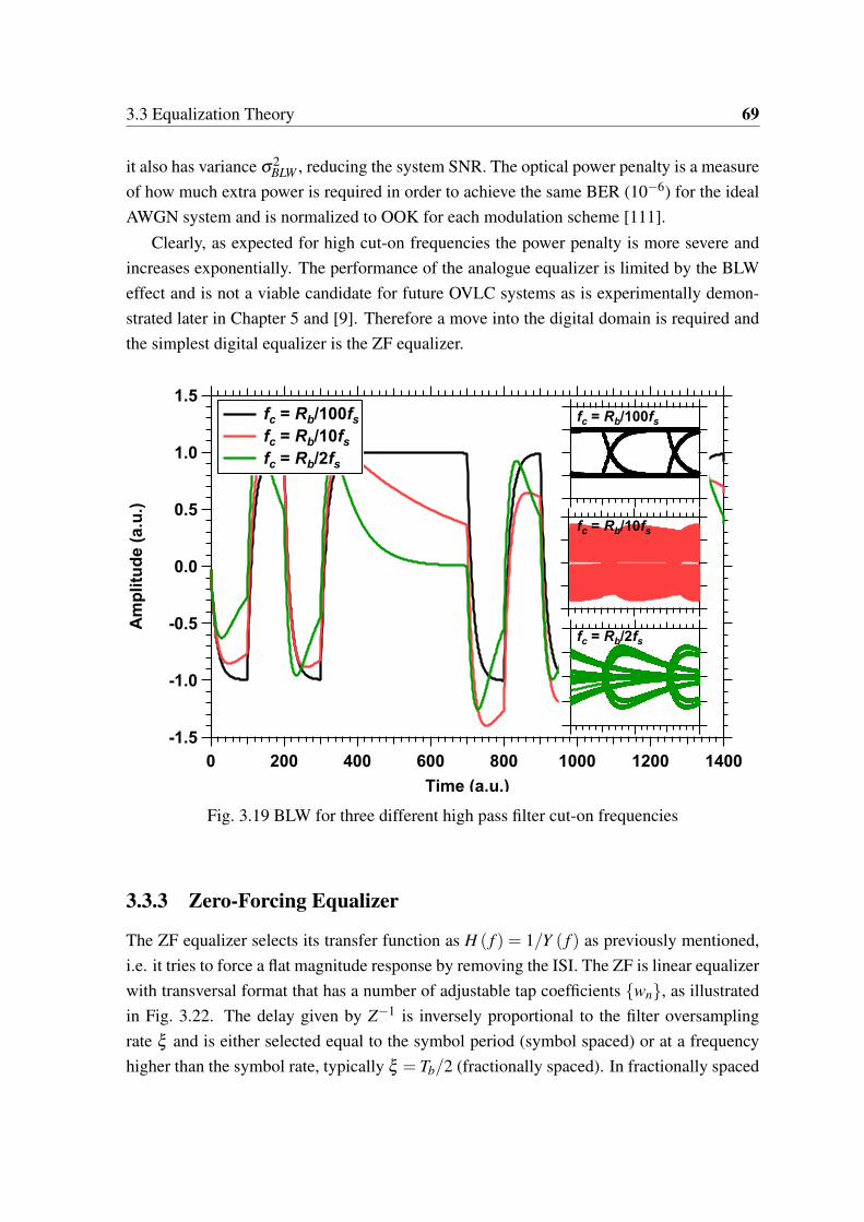
3.3 Equalization Theory 69
it also has variance σ2BLW , reducing the system SNR. The optical power penalty is a measure
of how much extra power is required in order to achieve the same BER (10−6) for the idealAWGN system and is normalized to OOK for each modulation scheme [111].
Clearly, as expected for high cut-on frequencies the power penalty is more severe andincreases exponentially. The performance of the analogue equalizer is limited by the BLWeffect and is not a viable candidate for future OVLC systems as is experimentally demon-strated later in Chapter 5 and [9]. Therefore a move into the digital domain is required andthe simplest digital equalizer is the ZF equalizer.
-1.5
-1.0
-0.5
0.0
0.5
1.0
1.5
Am
plitu
de (
a.u
.)
1400120010008006004002000
Time (a.u.)
fc = Rb/100fs
fc = Rb/10fs
fc = Rb/2fs
fc = Rb/100fs fc = Rb/10fs fc = Rb/2fs
Fig. 3.19 BLW for three different high pass filter cut-on frequencies
3.3.3 Zero-Forcing Equalizer
The ZF equalizer selects its transfer function as H ( f ) = 1/Y ( f ) as previously mentioned,i.e. it tries to force a flat magnitude response by removing the ISI. The ZF is linear equalizerwith transversal format that has a number of adjustable tap coefficients wn, as illustratedin Fig. 3.22. The delay given by Z−1 is inversely proportional to the filter oversamplingrate ξ and is either selected equal to the symbol period (symbol spaced) or at a frequencyhigher than the symbol rate, typically ξ = Tb/2 (fractionally spaced). In fractionally spaced
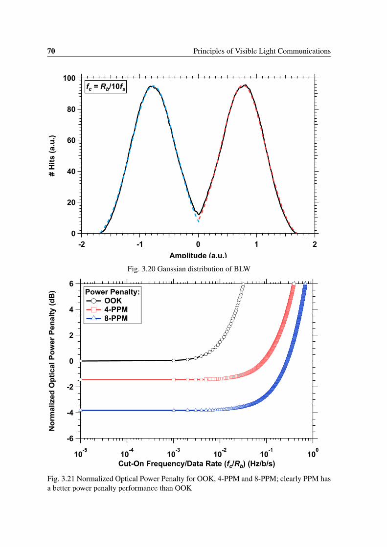
70 Principles of Visible Light Communications
100
80
60
40
20
0
# H
its (
a.u
.)
-2 -1 0 1 2
Amplitude (a.u.)
fc = Rb/10fs
Fig. 3.20 Gaussian distribution of BLW
-6
-4
-2
0
2
4
6
No
rma
lize
d O
pti
ca
l P
ow
er
Pe
na
lty
(d
B)
10-5
10-4
10-3
10-2
10-1
100
Cut-On Frequency/Data Rate (fc/Rb) (Hz/b/s)
Power Penalty: OOK 4-PPM 8-PPM
Fig. 3.21 Normalized Optical Power Penalty for OOK, 4-PPM and 8-PPM; clearly PPM hasa better power penalty performance than OOK

3.3 Equalization Theory 71
configuration the output of the filter is also sampled at this rate, as opposed to the symbolrate.
The impulse response of the ZF is given by [44]:
q(t) =N
∑n=−N
wnY(t −nξ ) (3.47)
where Y (t) is the incoming impulse response and is built up into an N ×N matrix in orderto find the transfer function of the system. The number of taps must be selected in order tospan the entire length of the ISI and is must be symmetrical around the current sample totake into account the previous and next samples, i.e. L ≤ 2N +1 where L is the number ofsamples that the ISI spans and N is introduced as a factor in order to make the number oftaps symmetrical around the current sample.
The condition to force zero ISI is given in Equation (3.38) and can be equated to q(t).Sampling the output at the symbol rate t = mTb leads to [44]:
q(mTb) =N
∑n=−N
wnY(mTb −nξ ) =
1 if m = 0
0 if m =±1, ±2, . . . , ±N(3.48)
The output of the filter can be displayed in matrix form as follows:
y0 · · · y−N · · · y−2N
.... . .
... . .. ...
yN · · · y0 · · · y−N
... . .. ...
. . ....
y2N · · · yN · · · y0
w−N
...
w0
...
wN
=
0...
1...
0
(3.49)
Therefore the tap coefficients are found by training the equalizer. A known sequence (i.e. asingle pulse) is transmitted over the system in order to formulate the channel response. Inthe ZF method all of the weights are updated at the same time as follows:
w = Y−1q (3.50)
where q represents the impulse response observation vector of the system. When all of thesymbols in the observation vector are considered for calculating the weights and error, thisis known as the least squares method.

72 Principles of Visible Light Communications
The filter coefficients are then convoluted into the system and periodically updated incase the system response has been modified in some way. Clearly a training sequence isrequired here in order to build up the impulse response of the system; the longer the trainingsequence is the better the representation of the system response becomes.
It is crucial to notice that the ZF is clearly very susceptible to the effects of noise asany random noise in the training sequence will cause an inaccurate picture of the systemresponse. VLC systems generally exhibit very large SNRs; however the power penalty forexceeding the system bandwidth is significant, thus the ZF is not the optimal equalizer forVLC systems.
yn
qn
dn
× × ×× ×
Z-1Z-1Z-1Z-1
wn
wn+1
wn+2
wn-1
wn-2
Equalizer
Σ
Fig. 3.22 Zero forcing equalizer in linear transversal filter format; it should be noted that thenomenclature yn is exactly the same as y(n)
3.3.4 Adaptive Linear Equalizer
An increase in performance can be obtained if an adaptive algorithm is introduced to findthe tap weights as illustrated by Fig. 3.23. There are several adaptive algorithms, mostnotable are the least mean squares (LMS) and recursive least squares (RLS) and the othersare typically variations of these algorithms. In order to find the tap weights the adaptivealgorithm requires training against a header sequence of data symbols that is known at thereceiver.
Least Mean Squares
The LMS algorithm is a gradient vector descent (based on the minimum square error crite-rion) on an error cost function E
e2(n)
and is very simple to implement due to the lack of
matrix inversions or correlation function calculations. The tap weights are given by [2]:
w(n+1) = w(n)+12
µ[−∇
(E
e2 (n))]
(3.51)
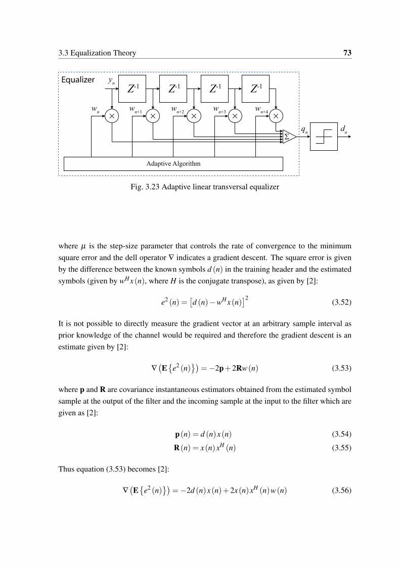
3.3 Equalization Theory 73
yn
qn
dn
× × ×× ×
Z-1Z-1Z-1Z-1
Adaptive Algorithm
wn+2
wn+3
wn+4
wn+1
wn
Equalizer
Σ
Fig. 3.23 Adaptive linear transversal equalizer
where µ is the step-size parameter that controls the rate of convergence to the minimumsquare error and the dell operator ∇ indicates a gradient descent. The square error is givenby the difference between the known symbols d (n) in the training header and the estimatedsymbols (given by wHx(n), where H is the conjugate transpose), as given by [2]:
e2 (n) =[d (n)−wHx(n)
]2(3.52)
It is not possible to directly measure the gradient vector at an arbitrary sample interval asprior knowledge of the channel would be required and therefore the gradient descent is anestimate given by [2]:
∇(E
e2 (n))
=−2p+2Rw(n) (3.53)
where p and R are covariance instantaneous estimators obtained from the estimated symbolsample at the output of the filter and the incoming sample at the input to the filter which aregiven as [2]:
p(n) = d (n)x(n) (3.54)
R(n) = x(n)xH (n) (3.55)
Thus equation (3.53) becomes [2]:
∇(E
e2 (n))
=−2d (n)x(n)+2x(n)xH (n)w(n) (3.56)

74 Principles of Visible Light Communications
Hence, the tap weight update equation is modified to [2]:
w(n+1) = w(n)+µx(n)[−d (n)x(n)+ xH (n)w(n)
](3.57)
Thus, the LMS algorithm can be summed up in three key equations, the filter output, esti-mation error and tap weight update equation, respectively [2]:
y(n) = wH (n)x(n) (3.58)
e(n) = d (n)− y(n) (3.59)
w(n+1) = w(n)+µx(n)[−d (n)x(n)+ xH (n)w(n)
](3.60)
At n = 0 the weight values are arbitrary and are traditionally set as zero and the step-sizeparameter is selected as 0 < µ < 1.
The RLS algorithm is now introduced and a comparison of LMS and RLS will follow.
Recursive Least Squares
The major difference between the RLS and LMS algorithms is that the RLS algorithm recur-sively reduces the linear least squares weighted error cost function while the LMS algorithmaims to reduce the mean square error.
A weighting factor β (i,n) (where i is the length of observable data in the filter and n isstill the sampling instance) must be introduced to the RLS error cost function ε (i) [2]:
ε (i) =i
∑n
β (i,n) |e(n)|2 (3.61)
where e(n) is the same as equation (3.59), i.e. the difference between desired and estimatedresponses. The vector input to the filter is given by [2]:
x(n) = [x(n) , x(n−1) , . . . , x(n−M+1)]T (3.62)
where T is the vector transpose and M is the number of taps. The weight vector is given by[2]:
w(i) = [w0 (i) , w1 (i−1) , . . . , wM−1 (i−M+1)]T (3.63)
The weighting factor is also known as the forgetting factor (0 < β (i,n)≤ 1) is generallyexpressed in exponential terms and is used to control the influence of previous data sampleson the current sample which is advantageous in a time varying environment. The forgetting

3.3 Equalization Theory 75
factor is given exponentially by [2]:
β (i,n) = λi−n (3.64)
The error cost function is therefore updated to [2]:
ε (n) =i
∑n
λi−n |e(n)|2 (3.65)
Before minimizing the error cost, the so-called normal equations are introduced which es-tablish the input correlation matrix Φ(n) and the cross-correlation matrix z(n) to find theoptimum tap weight values [2]:
Φ(i)w(i) = z(i) (3.66)
where the (M×M) input correlation matrix is given by [2]:
Φ(i) =i
∑n
λi−nx(n)x(n)H (3.67)
The cross-correlation vector finds the agreement between the input samples to each tap andthe desired response and is defined by [2]:
z(i) =i
∑n
λi−nx(n)d (n) (3.68)
Reformulating equation (3.67) to sum every term except n = i yields [2]:
Φ(i) =
[i−1
∑n
λi−1−nx(i)x(i)H
]λ +x(i)x(i)H (3.69)
which is an important result as the expression inside the brackets is the previous input cor-relation matrix and can therefore be rewritten to show a clear recursion [2]:
Φ(i) = λΦ(i−1)+x(i)x(i)H (3.70)
The term to the right of the addition operand is known as the correction term when updatingthe taps. The cross-correlation matrix can be shown recursively following the same method
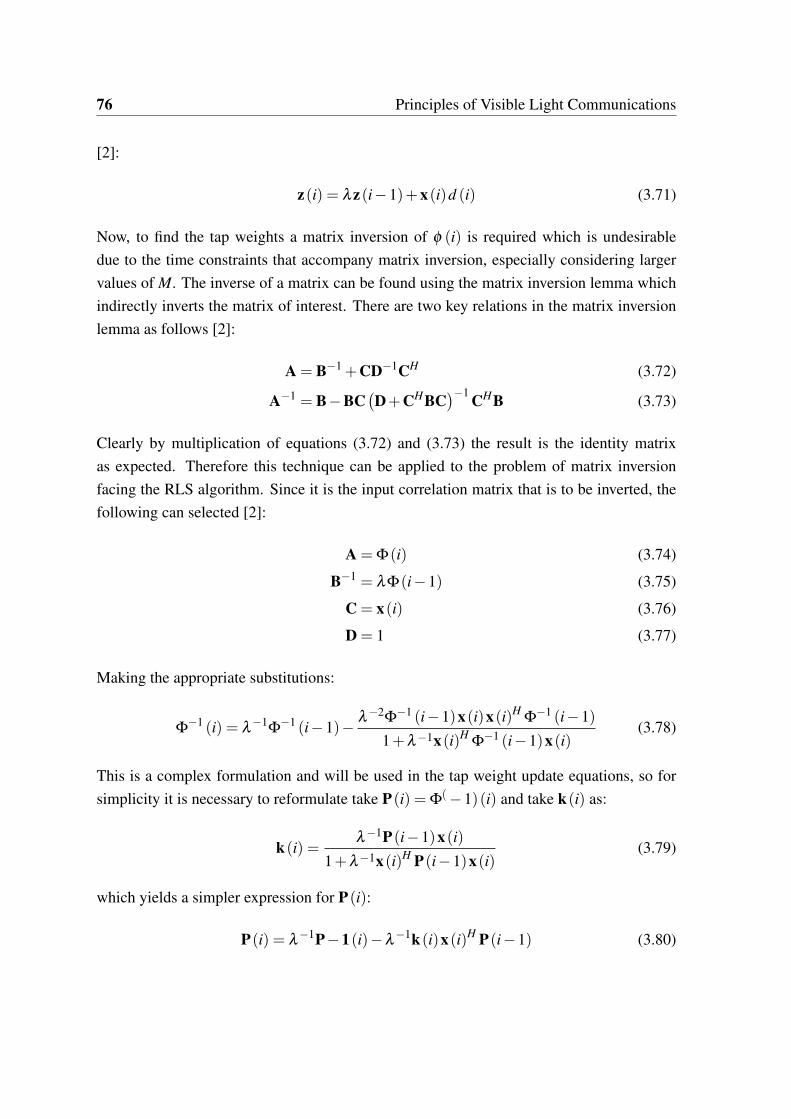
76 Principles of Visible Light Communications
[2]:
z(i) = λz(i−1)+x(i)d (i) (3.71)
Now, to find the tap weights a matrix inversion of φ (i) is required which is undesirabledue to the time constraints that accompany matrix inversion, especially considering largervalues of M. The inverse of a matrix can be found using the matrix inversion lemma whichindirectly inverts the matrix of interest. There are two key relations in the matrix inversionlemma as follows [2]:
A = B−1 +CD−1CH (3.72)
A−1 = B−BC(D+CHBC
)−1 CHB (3.73)
Clearly by multiplication of equations (3.72) and (3.73) the result is the identity matrixas expected. Therefore this technique can be applied to the problem of matrix inversionfacing the RLS algorithm. Since it is the input correlation matrix that is to be inverted, thefollowing can selected [2]:
A = Φ(i) (3.74)
B−1 = λΦ(i−1) (3.75)
C = x(i) (3.76)
D = 1 (3.77)
Making the appropriate substitutions:
Φ−1 (i) = λ
−1Φ
−1 (i−1)− λ−2Φ−1 (i−1)x(i)x(i)H
Φ−1 (i−1)
1+λ−1x(i)HΦ
−1 (i−1)x(i)(3.78)
This is a complex formulation and will be used in the tap weight update equations, so forsimplicity it is necessary to reformulate take P(i) = Φ
(−1)(i) and take k(i) as:
k(i) =λ−1P(i−1)x(i)
1+λ−1x(i)H P(i−1)x(i)(3.79)
which yields a simpler expression for P(i):
P(i) = λ−1P−1(i)−λ
−1k(i)x(i)H P(i−1) (3.80)
3.3 Equalization Theory 77
Rearranging equation (3.79) to show that k(i) is a function of P(i) yields:
k(i) = x(i)[λ−1P(i−1)−λ
−1k(i)x(i)H P(i−1)]= P(i)x(i) (3.81)
Thus the so-called gain vector which is the transformation of the filter input by the correla-tion matrix and is given by [2]:
k(i) = Φ(i)x(i) (3.82)
Updating the taps requires knowledge of the input correlation matrix and cross-correlationmatrix as the update is based on the previous values, thus the previous mathematics is crucialto updating the taps and it is trivial to notice that the RLS algorithm is significantly morecomplex than the LMS. The tap weight updates as follows, using equation (3.66) and (3.71)by [2]:
w(i) = Φ−1 (i)z(i) = P(i) [λz(i−1)+x(i)d (i)] (3.83)
Substituting equation (3.80) for P(i) and recalling equation (3.82), a recursive update can bedemonstrated [2]:
w(i) = w(i−1)+k(i)ξ (i) (3.84)
where ξ (i) = d (i)−wH (i−1)x(i) is the a priori estimation error where the product ofwH (n−1)x(n) is the estimate of the symbol using the previous tap weights. The a priorierror is cascaded back into the algorithm to update the taps while there is also the a posteriorierror which is the error out of the filter based on the current set of weights, i.e. e(i) =d (i)−wH (i)x(i).
To sum up, in order to implement the RLS algorithm, the following equations are re-quired in this order:
k(i) =λ−1P(i−1)x(i)
1+λ−1x(i)H P(i−1)x(i)(3.85)
ξ (i) = d (i)−wH (i−1)x(i) (3.86)
w(i) = w(i−1)+k(i)ξ (i) (3.87)
P(i) = λ−1P−1(i)−λ
−1k(i)x(i)H P(i−1) (3.88)
Then repeated this sequence for each sample until an acceptable error level is met or thetraining interval ends.
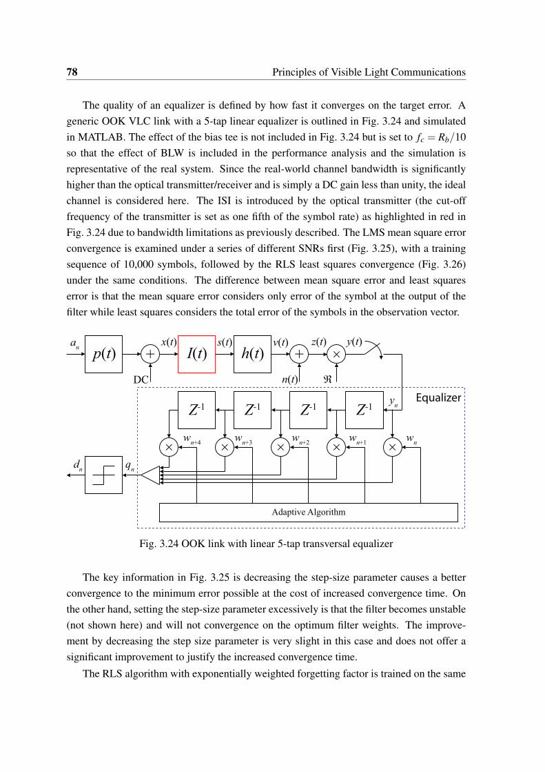
78 Principles of Visible Light Communications
The quality of an equalizer is defined by how fast it converges on the target error. Ageneric OOK VLC link with a 5-tap linear equalizer is outlined in Fig. 3.24 and simulatedin MATLAB. The effect of the bias tee is not included in Fig. 3.24 but is set to fc = Rb/10so that the effect of BLW is included in the performance analysis and the simulation isrepresentative of the real system. Since the real-world channel bandwidth is significantlyhigher than the optical transmitter/receiver and is simply a DC gain less than unity, the idealchannel is considered here. The ISI is introduced by the optical transmitter (the cut-offfrequency of the transmitter is set as one fifth of the symbol rate) as highlighted in red inFig. 3.24 due to bandwidth limitations as previously described. The LMS mean square errorconvergence is examined under a series of different SNRs first (Fig. 3.25), with a trainingsequence of 10,000 symbols, followed by the RLS least squares convergence (Fig. 3.26)under the same conditions. The difference between mean square error and least squareserror is that the mean square error considers only error of the symbol at the output of thefilter while least squares considers the total error of the symbols in the observation vector.
p(t) I(t) h(t) ++
×
ℜn(t)DC
x(t) s(t) v(t) z(t) y(t)an
yn
qn
dn
××× ××
Z-1Z-1Z-1Z-1
Adaptive Algorithm
Equalizer
wn+2
wn+1
wn
wn+3
wn+4
Fig. 3.24 OOK link with linear 5-tap transversal equalizer
The key information in Fig. 3.25 is decreasing the step-size parameter causes a betterconvergence to the minimum error possible at the cost of increased convergence time. Onthe other hand, setting the step-size parameter excessively is that the filter becomes unstable(not shown here) and will not convergence on the optimum filter weights. The improve-ment by decreasing the step size parameter is very slight in this case and does not offer asignificant improvement to justify the increased convergence time.
The RLS algorithm with exponentially weighted forgetting factor is trained on the same

3.3 Equalization Theory 79
dataset and generally demonstrates much faster convergence than LMS as illustrated inFig. 3.26, although not always to a lower error in the case of small forgetting factors (notethe difference in range on the y-axis). An increasing forgetting factor offers a faster conver-gence to the least squares error than the LMS equalizer at a lower error value and there islittle difference in performance in each SNR case.
As illustrated by Fig. 3.25 and Fig. 3.26, the RLS algorithm is much faster to convergethan the LMS which comes at the cost of increased complexity. The DF equalizer can betrained with both the LMS and RLS algorithms and offers an improvement in performanceover the linear equalizer.
3.3.5 Decision Feedback Equalizer
The performance of an equalizer is directly related to the severity of the ISI experiencedin the system. In heavy ISI linear equalizers will fail due to their inability to produce non-linear relationships between input and output. Further, if a system transfer function exhibitsa deep spectral null a linear equalizer will struggle to compensate as it will set some ofthe tap coefficients to be excessively high [44]. Therefore it is necessary to introduce thenon-linear DF equalizer which works on the principle of estimating the influence of ISI inthe current symbol based upon the previously detected symbol. Two filters are required, thefeedforward and feedback filters. The feedforward filter is exactly the same as the adaptivelinear filters in the previous section and operates in the same way while the feedback filter ismade up of past symbols in order to estimate the contribution of ISI on the current symbol.The output of each filter is subtracted and a decision is made as follows:
qm =N1
∑i=0
cnym−n −N2
∑i=1
bndm−n (3.89)
where cn is coefficient value of the ith feedforward tap and ym−n is the current symbol. Theestimate of the previous symbol is given by dm−n and the feedback filter tap coefficients aregiven by bn.
The DF equalizer is not examined in this thesis but is briefly introduced since it shouldoffer a level of performance somewhere between the linear equalizer and the ANNs that areintroduced in the next section.
3.3.6 Equalization as a Classification Problem
While traditional equalizers such as the ones shown in the previous section are very popularthey do not offer the best performance. ANN classifiers were first introduced in by McCul-
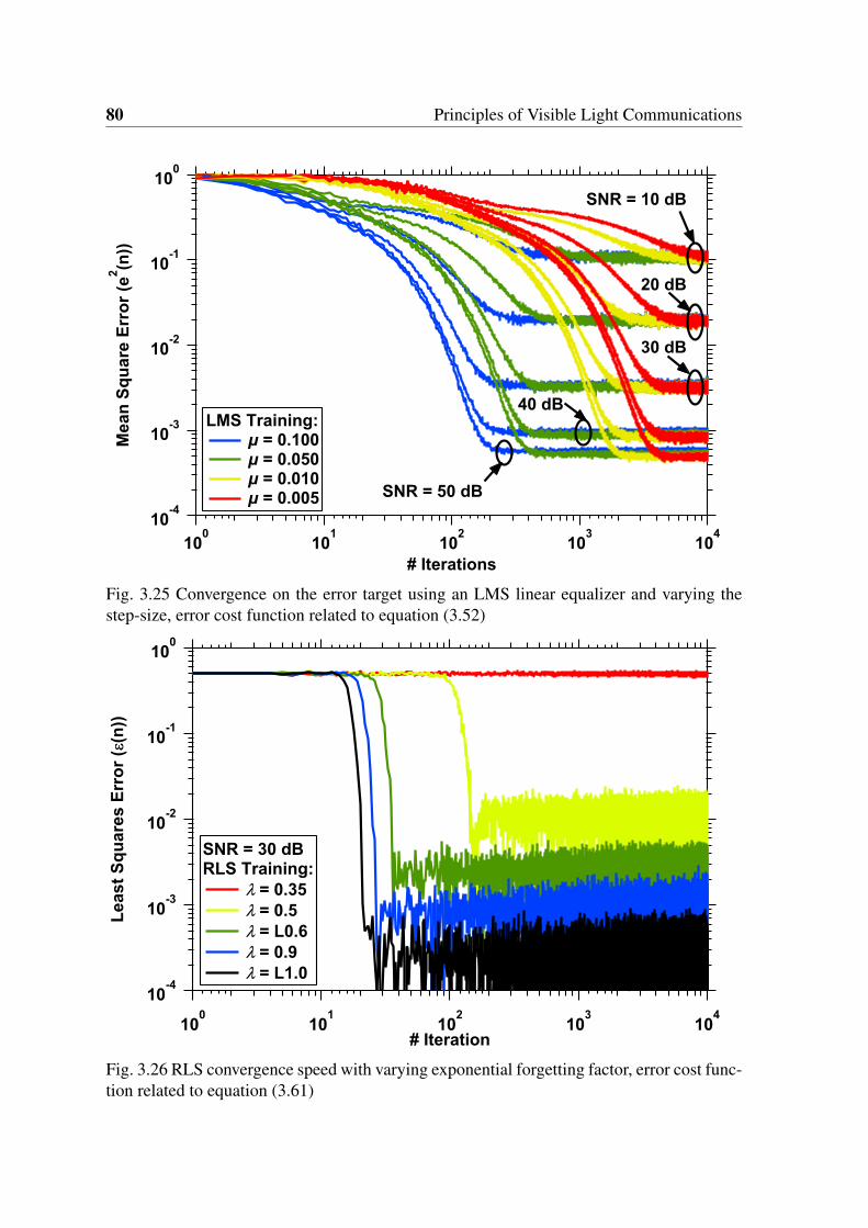
80 Principles of Visible Light Communications
10-4
10-3
10-2
10-1
100
Me
an
Sq
ua
re E
rro
r (e
2(n
))
100
101
102
103
104
# Iterations
SNR = 10 dB
SNR = 50 dB
20 dB
30 dB
40 dBLMS Training:
µ = 0.100 µ = 0.050 µ = 0.010 µ = 0.005
Fig. 3.25 Convergence on the error target using an LMS linear equalizer and varying thestep-size, error cost function related to equation (3.52)
10-4
10-3
10-2
10-1
100
Least
Sq
uare
s E
rro
r (e
(n))
100
101
102
103
104
# Iteration
SNR = 30 dBRLS Training:
l = 0.35
l = 0.5
l = L0.6
l = 0.9
l = L1.0
Fig. 3.26 RLS convergence speed with varying exponential forgetting factor, error cost func-tion related to equation (3.61)
3.3 Equalization Theory 81
loch and Pitts in 1943 [118] but did not gain popularity for a number of years due to theirhigh computational complexity that was simply not available at the time. ANNs were theneffectively forgotten until a re-emergence in the 1960s due to advances in perceptrons [119].Based on the results in [119] which showed that perceptrons do not always converge on thecorrect pattern due to some theoretical limits, a further lull was experienced in the popular-ity of ANNs for another two decades. Research interest has been renewed somewhat withadvances in signal processing and computational technologies. A complete ANN historycan be found in [120] and there are many applications for ANNs across many industriesincluding finance [121], medical imaging [122] and pattern recognition [123].
One of the most common applications is as equalizers in communications systems whichoperate based on forming decision boundaries based on a training scheme. This is in oppo-sition to calculating the contribution of ISI from each received symbol such as transversalequalizers. The decision boundaries formed aim to classify the received symbols into groupsthat belong to the desired symbol value. The boundaries are formed using neurons whichcan be thought of as being similar to those found in the human brain (see Table 3.1 fora comparison between computer and biological systems) and adjust their size in reactionto the training sequence such as tap weights in transversal filters. The major difference be-tween ANNs and transversal equalizers is the structure; the former are arranged into a highlyparallel form that allows non-linear mapping as each input is connected to each neuron. Thelatter are obviously highly linear (not considering DF) since each input is connected only toits corresponding weight. The schematic of a single neuron is shown in Fig. 3.27.
Each neuron in the network has a number of associated weights. The contribution fromeach input that is scaled by the weight is then summed. The summation can be biased usingan external input but in this thesis there is no bias so it is not considered any further. Theoutput of the summation uk is given by [124]:
uk = bk +N
∑i=1
x jwk j (3.90)
where the Nth input is given by xN and the weight associated with the Nth input is given bywkN . The output of the activation function is given by [124]:
yk = ϕ (uk) (3.91)
The activation function can be any differentiable function but is most commonly one ofthree; the threshold function, the piecewise-linear function (see Fig. 3.28) and the (log)

82 Principles of Visible Light Communications
Table 3.1 Table comparing computer systems such as microprocessors or sequential logicwith biological (and pseudo-biological) systems such as the neural networks; adopted from[6, 13]
Computer System Biological System
Processor Complex SimpleHigh speed (ns) Low speed (ns)One A large number
Memory Localized DistributedAddressable Addressable
Computing Centralized DistributedSequential ParallelStored programs Supervised/self
Learning
Reliability Vulnerable Robust
Power Consumption High Low
sigmoid function, given by [124]:
ϕ =1
1+ e−αuk(3.92)
where α is the so-called slope parameter which has been varied as α = 0.1 : 0.1 : 5 inFig. 3.29, which shows the log-sigmoid function, one of the most popular activation func-tions for multilayer perceptrons.
This is due to its inherently non-linear structure which allows highly non-linear map-ping. Clearly as α → 0 the slope becomes increasingly linear and as α → ∞ the log-sigmoidfunction first approximates to the piecewise linear function, then to the threshold function.
There are many ANN architectures that can be used as equalizers in communicationssystems; including single and multilayer feedforward networks, and feedback networks.The topologies of each network are shown in Fig. 3.30, Fig. 3.31 and Fig. 3.32 for single,multilayer and DF networks, respectively.
The number of layers does not include the input layer since no processing occurs, soin single layer networks the neurons and activation function make up the output layer aspreviously in Fig. 3.27 while the inputs are generated using tap delay lines. Single layernetworks cannot extract higher order statistics from the data and there is requirement formultilayer networks that can (assuming there is a sufficient amount of neurons) form arbi-trarily complex decision boundaries, see Fig. 3.33.

3.3 Equalization Theory 83
x1
x2
xN
b
Σ ϕ(.)
wk1
wk2
wkN
uk
yk
....................
....................
WeightsInputs
Activation function
Fig. 3.27 Simple overview of a neuron
Multilayer networks consist of at least two layers (not including the input layer as men-tioned) where any layers between the input and output layers are so-called hidden layerswhich simply contain neurons. In general a two layer feedforward network is sufficient forequalization [59, 105, 125].
DF-ANNs are similar to multilayer networks except the output is fed back into one ormore inputs which offer a performance increase in the same way DF equalizers offer animprovement over linear transversal equalizers. It is clear from comparison of Fig. 3.31 andFig. 3.32 that there is no difference in computational complexity between the DF-ANN andmultilayer ANN.
For equalization using classification, ANNs require training similar to transversal equal-izers. The training sequence simply allows the ANN to adjust the neuron weights accordingto a gradient descent on the error cost function is satisfied. There are a number of train-ing methods including LMS and RLS and scaled conjugate gradient (SCG) learning but themost popular is the Levenberg-Marquardt back propagation (LMBP) algorithm because itis simple to implement in hardware due to low complexity but requires the most memory.SCG training should converge to a lower error value but requires a longer training periodand is more complex for hardware implementation so is not examined here. Having a shorttraining sequence is of paramount importance because it reduces the amount of redundancyin the system, especially if the system is non-stationary and therefore requires frequent re-training to update the input-output map.

84 Principles of Visible Light Communications
1.0
0.8
0.6
0.4
0.2
0.0
Acti
vati
on
Fu
ncti
on
Ou
tpu
t (a
.u.)
-2 -1 0 1 2
Activation Function Input (a.u.)
Threshold Piecewise Linear
Fig. 3.28 Normalized threshold and piecewise linear activation functions
Fig. 3.29 Log-sigmoid activation function with α = 0.1 : 0.1 : 5

3.3 Equalization Theory 85
Input Layer Output Layer
x1
x2
x3
y1
y2
Fig. 3.30 Single layer ANNInput Layer Output Layer
x1
x2
x3
y1
Hidden Layer
Fig. 3.31 Multilayer ANN
Levenberg-Marquardt Back Propagation Algorithm
The error cost function (e(n)) is no different to the same function described in the LMS andRLS algorithms; i.e. the difference between the desired symbols and the received symbols.The neuron weights are updates as follows [124]:
wk j (n+1) = wk j (n)−η∂E (n)
∂wk j (n)(3.93)
where E (n) is the error cost function and η is the learning rate parameter. Immediately itis noticeable that the weight updates have an important difference between the previouslyoutlined algorithms; that is there is no matrix inversion which reduces the training com-
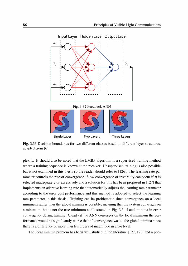
86 Principles of Visible Light Communications
Input Layer Output Layer
x1
x2
x3
y1
Hidden Layer
Fig. 3.32 Feedback ANN
Single Layer Two Layers Three Layers
Fig. 3.33 Decision boundaries for two different classes based on different layer structures,adapted from [6]
plexity. It should also be noted that the LMBP algorithm is a supervised training methodwhere a training sequence is known at the receiver. Unsupervised training is also possiblebut is not examined in this thesis so the reader should refer to [126]. The learning rate pa-rameter controls the rate of convergence. Slow convergence or instability can occur if η isselected inadequately or excessively and a solution for this has been proposed in [127] thatimplements an adaptive learning rate that automatically adjusts the learning rate parameteraccording to the error cost performance and this method is adopted to select the learningrate parameter in this thesis. Training can be problematic since convergence on a localminimum rather than the global minima is possible, meaning that the system converges ona minimum that is not the true minimum as illustrated in Fig. 3.34 Local minima in errorconvergence during training. Clearly if the ANN converges on the local minimum the per-formance would be significantly worse than if convergence was to the global minima sincethere is a difference of more than ten orders of magnitude in error level.
The local minima problem has been well studied in the literature [127, 128] and a pop-
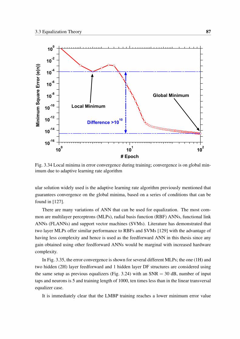
3.3 Equalization Theory 87
10-16
10
-14
10-12
10
-10
10-8
10-6
10-4
10-2
100
Min
imu
m S
qu
are
Err
or
(e(n
))
100
101
102
# Epoch
Local Minimum
Global Minimum
Difference >1010
Fig. 3.34 Local minima in error convergence during training; convergence is on global min-imum due to adaptive learning rate algorithm
ular solution widely used is the adaptive learning rate algorithm previously mentioned thatguarantees convergence on the global minima, based on a series of conditions that can befound in [127].
There are many variations of ANN that can be used for equalization. The most com-mon are multilayer perceptrons (MLPs), radial basis function (RBF) ANNs, functional linkANNs (FLANNs) and support vector machines (SVMs). Literature has demonstrated thattwo layer MLPs offer similar performance to RBFs and SVMs [129] with the advantage ofhaving less complexity and hence is used as the feedforward ANN in this thesis since anygain obtained using other feedforward ANNs would be marginal with increased hardwarecomplexity.
In Fig. 3.35, the error convergence is shown for several different MLPs; the one (1H) andtwo hidden (2H) layer feedforward and 1 hidden layer DF structures are considered usingthe same setup as previous equalizers (Fig. 3.24) with an SNR = 30 dB, number of inputtaps and neurons is 5 and training length of 1000, ten times less than in the linear transversalequalizer case.
It is immediately clear that the LMBP training reaches a lower minimum error value
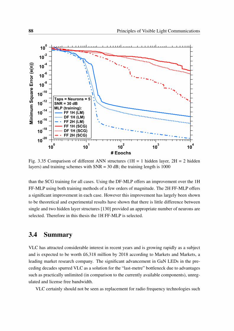
88 Principles of Visible Light Communications
10-20
10
-18
10-16
10
-14
10-12
10
-10
10-8
10-6
10-4
10-2
100
Min
imu
m S
qu
are
Err
or
(e(n
))
100
101
102
103
104
# Epochs
Taps = Neurons = 5SNR = 30 dBMLP (training):
FF 1H (LM) DF 1H (LM) FF 2H (LM) FF 1H (SCG) DF 1H (SCG) FF 2H (SCG)
Fig. 3.35 Comparison of different ANN structures (1H = 1 hidden layer, 2H = 2 hiddenlayers) and training schemes with SNR = 30 dB; the training length is 1000
than the SCG training for all cases. Using the DF-MLP offers an improvement over the 1HFF-MLP using both training methods of a few orders of magnitude. The 2H FF-MLP offersa significant improvement in each case. However this improvement has largely been shownto be theoretical and experimental results have shown that there is little difference betweensingle and two hidden layer structures [130] provided an appropriate number of neurons areselected. Therefore in this thesis the 1H FF-MLP is selected.
3.4 Summary
VLC has attracted considerable interest in recent years and is growing rapidly as a subjectand is expected to be worth £6,318 million by 2018 according to Markets and Markets, aleading market research company. The significant advancement in GaN LEDs in the pre-ceding decades spurred VLC as a solution for the “last-metre” bottleneck due to advantagessuch as practically unlimited (in comparison to the currently available components), unreg-ulated and license free bandwidth.
VLC certainly should not be seen as replacement for radio frequency technologies such
3.4 Summary 89
as Wi-Fi, but as a complimentary technology that can provide access in places where Wi-Ficannot such as hospitals and airplanes. Further VLC has a wider bandwidth (around 10,000times) than radio frequencies and therefore has the potential to significantly improve thetransmission speed to the end user.
A substantial amount of research has been conducted into intensity modulation schemesfor both VLC and indoor IR communications. The most popular are OOK because it isvery simple to implement and bandwidth efficient and L-PPM due to its power efficiencywhich often has more importance than bandwidth efficiency in optical links due to the highbandwidths. In general this thesis only investigates M-PAM and L-PPM for these reasons,however there are a number of standard techniques such as DMT and a plethora of noveltechniques that could equally be used in place of M-PAM and L-PPM.

Chapter 4
Visible Light Communications withOrganic Light Emitting Diodes
4.1 Introduction
In the next four chapters, four communications systems are analysed; VLC with an SMOLEDtransmitter and Si PIN PD receiver in this chapter, VLC with a WPLED transmitter and OPDas receiver in Chapter 5. In Chapter 6, a VLC link with an SMOLED transmitter and OPDreceiver is examined and finally in Chapter 7 a PLED transmitter and Si PD receiver link isexamined.
The general working principles of organic devices were given in Chapter 2 and are there-fore not covered here. The first commercial SMOLED used was an Osram Orbeos CMW-031 with 79 mm diameter and a luminous efficacy of 23 lm/W. The normalized measuredoptical spectrum is shown in Fig. 4.1 illustrating that the device is made from individualRGB components with peaks at 610 (R), 514 (G) and 480 (B) nm. The peak at 480 nm isnot as pronounced as the other peaks and this is attributed to the poor conversion efficiencyof blue materials in comparison to red and green [131, 132].
The empirically measured normalized azimuth emission profile of the SMOLED isshown in Fig. 4.2 along with the theoretical normalized Lambertian emission profile. Itis clear that the plots closely match and the OLED is approximately Lambertian in emissionwhich is supported in the literature [104, 133–135].
The OLED L-I-V curve was measured using the setup shown in Fig. 4.3 under au-tonomous LabVIEW control.
The measured intensity is a unit-less quantity which is relative to the integration timeand the sensitivity of the pixels. The integration time is set to 30 ms which was found

92 Visible Light Communications with Organic Light Emitting Diodes
1.0
0.8
0.6
0.4
0.2
0.0
Inte
nsit
y (
no
un
it)
800700600500400
Wavelength (nm)
SaturationCCD
480 nm
514 nm
610 nm
5.0
4.5
4.0
3.5
3.0
Vb
ias
(V)
Fig. 4.1 Optical spectrum of the Osram Orbeos CMW-031 SMOLED under test with peakwavelengths marked
0 0.2 0.4 0.6 0.8 1-90
-80
-70
-60
-50
-40
-30
-20-10 0 10
20
30
40
50
60
70
80
90
Emission Profile: OLED Lambertian
Angle (°)
Normalized Emission Power
Fig. 4.2 Polar plot showing the normalized measured emission profile of the SMOLED,which is in close agreement to the normalized Lambertian emission profile (m = 1)

4.1 Introduction 93
IOLED
LabVIEW
Control V
AgilentE3631A
ThorLabsCCS200
Fig. 4.3 Measurement setup for obtaining the SMOLED L-I-V curve
empirically. The measured intensity would be integrated over the active wavelengths forevery bias voltage if it were a continuous signal; however the discrete samples are summedin order to find the total light output as follows:
L =1n
n
∑λ=1
I (λ ) (4.1)
Then the L-I-V curve is produced as in Fig. 4.4. First note that the OLED goes througha transition phase where the optical power and voltage both drop as a function of time inthe first few hours of operation. This could be due to the thermal destruction of unstablemolecules and processing defects such as short circuits. This is a common feature of newSMOLEDs and PLEDs and is colloquially known as ‘burning-in’. The device then reachesa steady state region. Note that the data shown in Fig. 4.4 was for the first twelve hoursof seven days of continuous measurements. The device remains in the steady state for theremaining time.
The SMOLED bandwidth is measured using the setup in Fig. 4.5. A swept since wave(1 Vpp) is transmitted over the free space link. The bias tee has a cut-on frequency of 7kHz and the receiver used is a ThorLabs PDA36A-EC with in-built TIA set to 10 dB gain;reducing the Si PD bandwidth to 5 MHz. The entire system including the voltage source(Agilent E3631A) supplying the SMOLED bias voltage is controlled by LabVIEW.
The measured spectrum (measured at point X in Fig. 4.5) is shown in Fig. 4.6 and itsnormalized version is in Fig. 4.7 where the bias voltage is varied for each spectrum mea-surement. The injection current can be measured from the I-V curve in Fig. 4.4. The rangeof bias voltages is from 2.9 – 5 V. For voltages below 2.9 V, the SMOLED is effectively notswitched on, as can be inferred from Fig. 4.4
The ESA is not sensitive to frequencies below 9 kHz and therefore the attenuation ofthe low frequencies caused by the bias tee cannot be noticed. The output light intensity
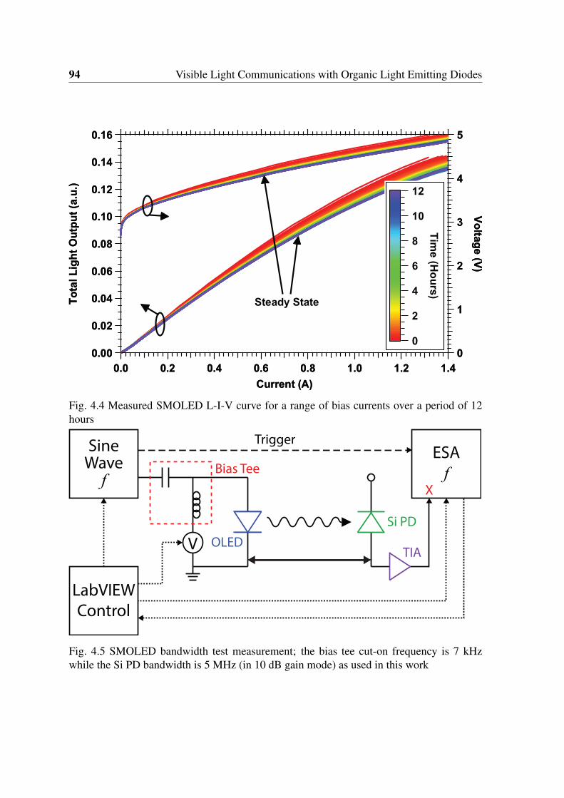
94 Visible Light Communications with Organic Light Emitting Diodes
Fig. 4.4 Measured SMOLED L-I-V curve for a range of bias currents over a period of 12hours
SineWavef
V
ESA
f
Trigger
Bias Tee
Si PD
OLEDTIA
LabVIEW
Control
X
Fig. 4.5 SMOLED bandwidth test measurement; the bias tee cut-on frequency is 7 kHzwhile the Si PD bandwidth is 5 MHz (in 10 dB gain mode) as used in this work
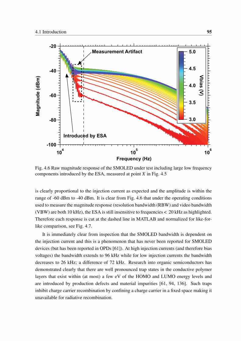
4.1 Introduction 95
Measurement Artifact
Ma
gn
itu
de
(d
Bm
)
Fig. 4.6 Raw magnitude response of the SMOLED under test including large low frequencycomponents introduced by the ESA, measured at point X in Fig. 4.5
is clearly proportional to the injection current as expected and the amplitude is within therange of -60 dBm to -40 dBm. It is clear from Fig. 4.6 that under the operating conditionsused to measure the magnitude response (resolution bandwidth (RBW) and video bandwidth(VBW) are both 10 kHz), the ESA is still insensitive to frequencies < 20 kHz as highlighted.Therefore each response is cut at the dashed line in MATLAB and normalized for like-for-like comparison, see Fig. 4.7.
It is immediately clear from inspection that the SMOLED bandwidth is dependent onthe injection current and this is a phenomenon that has never been reported for SMOLEDdevices (but has been reported in OPDs [61]). At high injection currents (and therefore biasvoltages) the bandwidth extends to 96 kHz while for low injection currents the bandwidthdecreases to 26 kHz; a difference of 72 kHz. Research into organic semiconductors hasdemonstrated clearly that there are well pronounced trap states in the conductive polymerlayers that exist within (at most) a few eV of the HOMO and LUMO energy levels andare introduced by production defects and material impurities [61, 94, 136]. Such trapsinhibit charge carrier recombination by confining a charge carrier in a fixed space making itunavailable for radiative recombination.
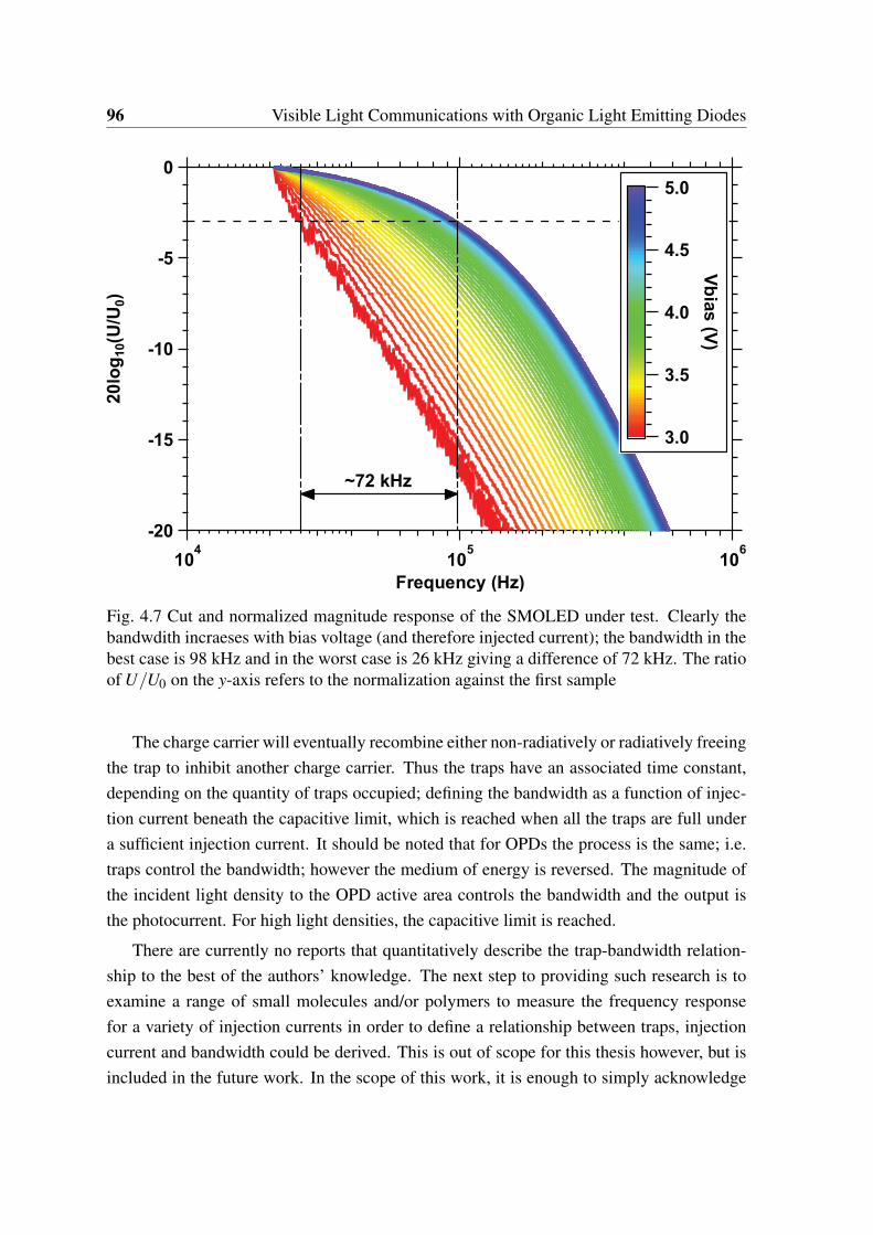
96 Visible Light Communications with Organic Light Emitting Diodes
Fig. 4.7 Cut and normalized magnitude response of the SMOLED under test. Clearly thebandwdith incraeses with bias voltage (and therefore injected current); the bandwidth in thebest case is 98 kHz and in the worst case is 26 kHz giving a difference of 72 kHz. The ratioof U/U0 on the y-axis refers to the normalization against the first sample
The charge carrier will eventually recombine either non-radiatively or radiatively freeingthe trap to inhibit another charge carrier. Thus the traps have an associated time constant,depending on the quantity of traps occupied; defining the bandwidth as a function of injec-tion current beneath the capacitive limit, which is reached when all the traps are full undera sufficient injection current. It should be noted that for OPDs the process is the same; i.e.traps control the bandwidth; however the medium of energy is reversed. The magnitude ofthe incident light density to the OPD active area controls the bandwidth and the output isthe photocurrent. For high light densities, the capacitive limit is reached.
There are currently no reports that quantitatively describe the trap-bandwidth relation-ship to the best of the authors’ knowledge. The next step to providing such research is toexamine a range of small molecules and/or polymers to measure the frequency responsefor a variety of injection currents in order to define a relationship between traps, injectioncurrent and bandwidth could be derived. This is out of scope for this thesis however, but isincluded in the future work. In the scope of this work, it is enough to simply acknowledge
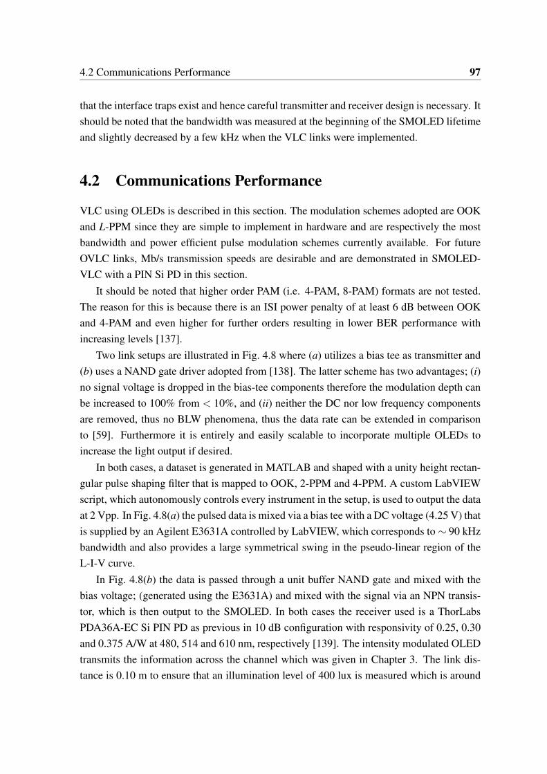
4.2 Communications Performance 97
that the interface traps exist and hence careful transmitter and receiver design is necessary. Itshould be noted that the bandwidth was measured at the beginning of the SMOLED lifetimeand slightly decreased by a few kHz when the VLC links were implemented.
4.2 Communications Performance
VLC using OLEDs is described in this section. The modulation schemes adopted are OOKand L-PPM since they are simple to implement in hardware and are respectively the mostbandwidth and power efficient pulse modulation schemes currently available. For futureOVLC links, Mb/s transmission speeds are desirable and are demonstrated in SMOLED-VLC with a PIN Si PD in this section.
It should be noted that higher order PAM (i.e. 4-PAM, 8-PAM) formats are not tested.The reason for this is because there is an ISI power penalty of at least 6 dB between OOKand 4-PAM and even higher for further orders resulting in lower BER performance withincreasing levels [137].
Two link setups are illustrated in Fig. 4.8 where (a) utilizes a bias tee as transmitter and(b) uses a NAND gate driver adopted from [138]. The latter scheme has two advantages; (i)no signal voltage is dropped in the bias-tee components therefore the modulation depth canbe increased to 100% from < 10%, and (ii) neither the DC nor low frequency componentsare removed, thus no BLW phenomena, thus the data rate can be extended in comparisonto [59]. Furthermore it is entirely and easily scalable to incorporate multiple OLEDs toincrease the light output if desired.
In both cases, a dataset is generated in MATLAB and shaped with a unity height rectan-gular pulse shaping filter that is mapped to OOK, 2-PPM and 4-PPM. A custom LabVIEWscript, which autonomously controls every instrument in the setup, is used to output the dataat 2 Vpp. In Fig. 4.8(a) the pulsed data is mixed via a bias tee with a DC voltage (4.25 V) thatis supplied by an Agilent E3631A controlled by LabVIEW, which corresponds to ∼ 90 kHzbandwidth and also provides a large symmetrical swing in the pseudo-linear region of theL-I-V curve.
In Fig. 4.8(b) the data is passed through a unit buffer NAND gate and mixed with thebias voltage; (generated using the E3631A) and mixed with the signal via an NPN transis-tor, which is then output to the SMOLED. In both cases the receiver used is a ThorLabsPDA36A-EC Si PIN PD as previous in 10 dB configuration with responsivity of 0.25, 0.30and 0.375 A/W at 480, 514 and 610 nm, respectively [139]. The intensity modulated OLEDtransmits the information across the channel which was given in Chapter 3. The link dis-tance is 0.10 m to ensure that an illumination level of 400 lux is measured which is around
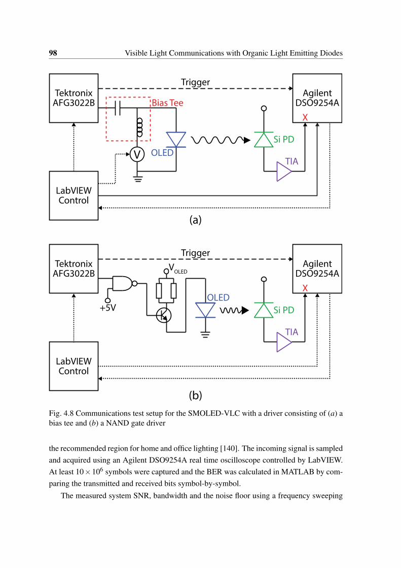
98 Visible Light Communications with Organic Light Emitting Diodes
TektronixAFG3022B
AgilentDSO9254A
LabVIEWControl
V
Trigger
Bias Tee
Si PD
OLEDTIA
TektronixAFG3022B
AgilentDSO9254A
LabVIEWControl
Trigger
Si PD
OLED
TIA
VOLED
(a)
(b)
+5V
X
X
Fig. 4.8 Communications test setup for the SMOLED-VLC with a driver consisting of (a) abias tee and (b) a NAND gate driver
the recommended region for home and office lighting [140]. The incoming signal is sampledand acquired using an Agilent DSO9254A real time oscilloscope controlled by LabVIEW.At least 10×106 symbols were captured and the BER was calculated in MATLAB by com-paring the transmitted and received bits symbol-by-symbol.
The measured system SNR, bandwidth and the noise floor using a frequency sweeping

4.2 Communications Performance 99
sine wave and an Agilent MXA N9010A electrical spectrum analyser as can be seen inFig. 4.9.
Fig. 4.9 Measured SNR (red) (left), system bandwidth (BW) (blue) (right) and receiver noise(black) (right)
The bandwidth and noise amplitudes referred to the right hand axis were measured di-rectly by the electrical spectrum analyser with the OLED on (bandwidth) and off (noise).The SNR was measured by subtracting the bandwidth and noise amplitudes and indicates ahigh quality signal with SNR > 30 dB for frequencies < 1 MHz. For frequencies > 1 MHzthe SNR quickly degrades. Note that at ∼ 2.7 MHz the SNR drops to ∼ 10 dB and at∼ 3 MHz the signal has descended into the noise floor.
4.2.1 On-Off Keying
The BER performance of both driving circuits is shown in Fig. 4.10. An improvement inachievable data rate of > 100 kb/s can be observed with the NAND driver over the bias-teedriver which can offer transmission speeds of 250 and 75 kb/s, respectively. Some insightinto the data rate increase can be provided by considering the frequency spectrum of eachdriver. In the bias-tee driver, the selection of capacitor is crucial as it has an associatedcut-on frequency fco. If the capacitor value is selected too high the cut-off frequency is

100 Visible Light Communications with Organic Light Emitting Diodes
reduced (which is desirable) but more power is dissipated meaning that the modulationdepth decreases. Improperly selecting too low means fco increases, inducing the BLWphenomena as the DC and low frequency components below fco are significantly attenuated.This is reflected in the magnitude response as illustrated in Fig. 4.11 which clearly showsthree sections of an arbitrary system with a bias tee driver that has similar characteristics toa band pass filter.
6
5
4
3
2
1
0
-lo
g1
0(B
ER
)
5004003002001000
Bit Rate (kb/s)
Driving Circuit: Coupling Capacitor NAND Gate Buffer
Fig. 4.10 BER performance of each driving circuit; data rates of 250 and 75 kb/s can beachieved using the NAND gate and bias tee drivers, respectively
In section A the low frequency components are attenuated, which is the root of the BLW.Sections B and C show a normal low pass response where all frequencies in section C areoutside the system modulation bandwidth. The difference in drivers is further reflected in theeye diagrams produced from the received symbols at 100 kb/s data rate shown in Fig. 4.12and Fig. 4.13 as in Fig. 4.11 there is a clearly a dominating BLW effect caused by the biastee driver. There have been studies to try and eliminate BLW such as the quantized feedbackbaseline restoration [141], which aims to restore the missing frequency components with afeedback filter, or using a subcarrier frequency in order to avoid the signal attenuation. Thismethod in particular is not ideal as it wastes the available bandwidth, thus reducing systemcapacity. It is noteworthy that BLW is approximately a random Gaussian process [41] so it
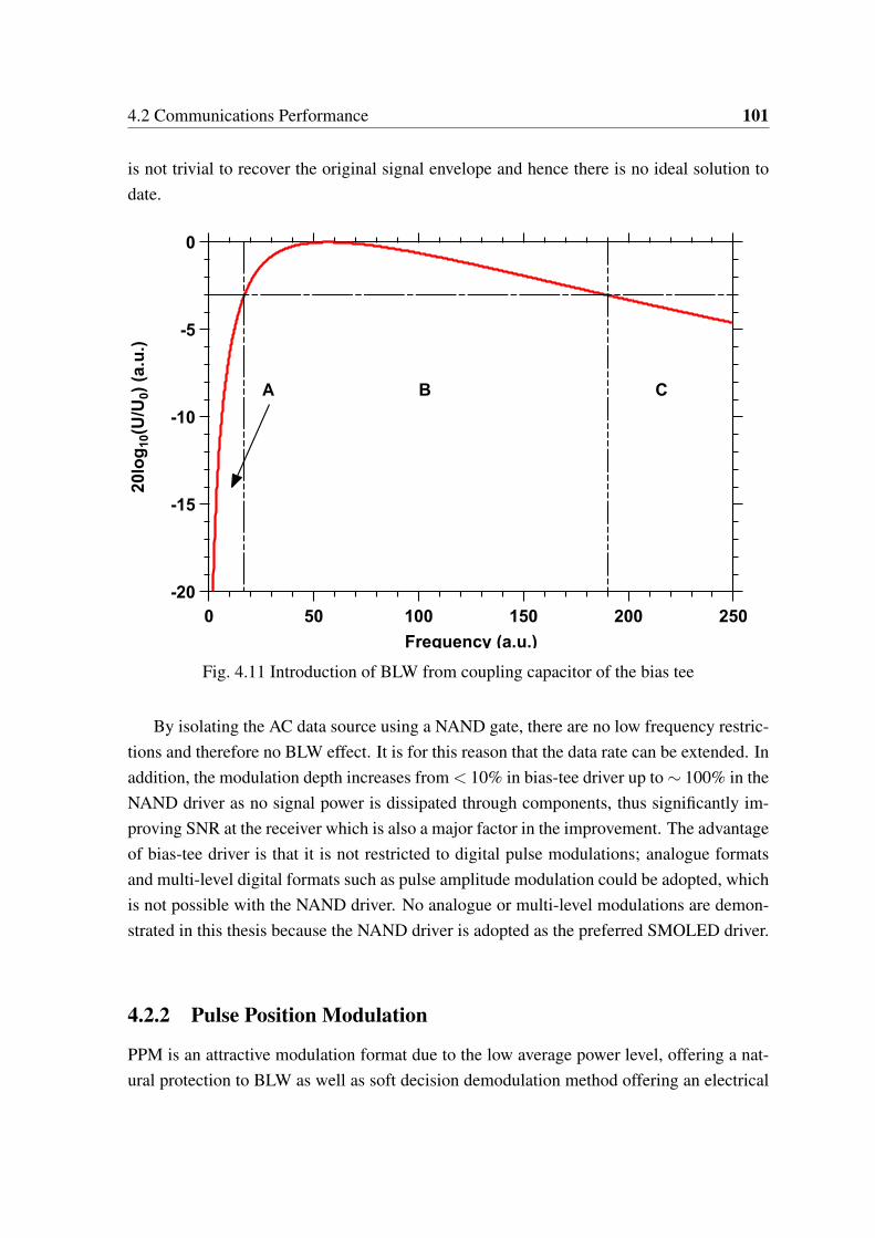
4.2 Communications Performance 101
is not trivial to recover the original signal envelope and hence there is no ideal solution todate.
-20
-15
-10
-5
0
20
log
10(U
/U0)
(a.u
.)
250200150100500
Frequency (a.u.)
A B C
Fig. 4.11 Introduction of BLW from coupling capacitor of the bias tee
By isolating the AC data source using a NAND gate, there are no low frequency restric-tions and therefore no BLW effect. It is for this reason that the data rate can be extended. Inaddition, the modulation depth increases from < 10% in bias-tee driver up to ∼ 100% in theNAND driver as no signal power is dissipated through components, thus significantly im-proving SNR at the receiver which is also a major factor in the improvement. The advantageof bias-tee driver is that it is not restricted to digital pulse modulations; analogue formatsand multi-level digital formats such as pulse amplitude modulation could be adopted, whichis not possible with the NAND driver. No analogue or multi-level modulations are demon-strated in this thesis because the NAND driver is adopted as the preferred SMOLED driver.
4.2.2 Pulse Position Modulation
PPM is an attractive modulation format due to the low average power level, offering a nat-ural protection to BLW as well as soft decision demodulation method offering an electrical

102 Visible Light Communications with Organic Light Emitting Diodes
Fig. 4.12 Eye diagram for bias tee driving circuit at 100 kb/s; there is a clear BLW effectperturbing the link quality
-1.5
-1.0
-0.5
0.0
0.5
1.0
1.5
Am
pli
tud
e (
a.u
.)
20151050
Time (µs)
Fig. 4.13 Eye diagram for the NAND gate driving circuit with a clear improvement over thebias tee driver

4.2 Communications Performance 103
SNR gain of 1.5 dB [115], however at the cost of increased bandwidth requirement [44].Therefore in this thesis only the lower orders of PPM (i.e. 2 and 4-PPM) are used. The slotrate and amplitude of 4-PPM is set to twice that of 2-PPM; which is in turn set to twice thatof OOK in order to provide the same transmission speeds. Therefore 4-PPM will requiretwice the bandwidth of 2-PPM (and four times that of OOK; since this system is bandlim-ited, no higher orders of PPM are tested i.e. 8-PPM because of the eight times bandwidthrequirement of OOK. Soft decision demodulation is not covered here as it is well-knownand can be referred to in [115]. The performance of all other pulse modulation formats layssomewhere between the bandwidth efficient OOK and the power efficient PPM [40] and thisis the reason that only OOK and PPM are examined.
The BER performance of 2 and 4-PPM with hard decision decoding using a thresholddetector is illustrated in Fig. 4.14 demonstrating transmission of 150 and 50 kb/s data ratesalong with the 250 kb/s OOK link for reference. In comparison to the ∼ 90 kHz systembandwidth bottleneck introduced by the SMOLED it was expected that OOK would offerthe best performance with no equalization as it has half the bandwidth requirement of 2-PPM and four times less than 4-PPM. Furthermore, as expected 2-PPM also outperforms4-PPM and this is also attributed to the lower bandwidth requirements.
6
5
4
3
2
1
0
-lo
g1
0(B
ER
)
0.50.40.30.20.10.0
Bit Rate (Mb/s)
Threshold: 2-PPM 4-PPM OOK
Fig. 4.14 Unequalized BER performance of each modulation

104 Visible Light Communications with Organic Light Emitting Diodes
The system BER performance using soft decision demodulation as a function of the bitrate is shown in Fig. 4.15. It is not possible to use the soft decision algorithm with OOK soonly 2 and 4-PPM with bit rates of 400 kb/s and 200 kb/s, respectively are used in this work.There is still a disparity between 2-PPM and 4-PPM caused by their respective bandwidthrequirements. Using soft decision demodulation offers a significant improvement in theavailable data rate in comparison to threshold detection. More specifically, the improvementin data rates for 2 and 4-PPM are 250 kb/s and 150 kb/s, respectively. This means that 2-PPM has been able to double its capacity while 4-PPM has improved by four times, whichis remarkable. These data rates obviously outperform OOK with threshold detection are justslightly short of the 550 kb/s as reported in [59] using an MLP-ANN equalizer.
In order to ensure that it is the filters that are being examined, a DSP board was selectedwhere the synchronization can be performed in the MATLAB domain. The clock speed ofthe DSP is 225 MHz, which is clearly well in excess of the requirements for this system.The DSP board is programmed using the TI Code Composer Studio (CCS) software andthe signal processing is implemented with the same features (i.e. number of taps in theequalizer case, or algorithm in soft demodulation case) as in the offline case for a like-for-like comparison. Since the adaptive algorithm was used it is not possible to give a generalfigure. The output of the DSP board is then recovered and transferred to the MATLABdomain for comparison with the offline DSP. It should also be noted that the data used in theoffline and online cases is not the same data in order to ensure the thorough examination ofthe online filters and ensure the comparisons are not influenced by the data sequence; thusensuring that the data is not biasing the result. This is reflected in Fig. 4.15 and Fig. 4.16,which show minor differences between the offline and online cases.
4.3 Equalization
As was outlined in Chapter 3 it is possible to observe equalization as a classification prob-lem rather than an information theory problem and thus using an ANN as a system responseequalizer. ANNs are the best performing transversal linear equalizer for both channel andsystem equalization [142]. This is because they are capable of mapping any input-outputsequence (linear or otherwise) and nullifying the negative effects that other equalizers strug-gle to cope with such as large spectral nulls. The MLP ANN is implemented here in order tomaximize the available data rates. The MLP is not the best performing ANN; however it isthe least complex and supports the Levenberg-Marquardt back-propagation (LMBP) algo-rithm, which is very popular due to the ease of hardware implementation [142]. The LMBPalgorithm is a supervised training method based on a gradient descent on the error cost func-
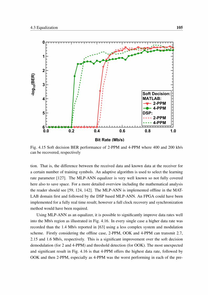
4.3 Equalization 105
6
5
4
3
2
1
0
-lo
g1
0(B
ER
)
1.00.80.60.40.20.0
Bit Rate (Mb/s)
Soft Decision:MATLAB:
2-PPM 4-PPM
DSP: 2-PPM 4-PPM
Fig. 4.15 Soft decision BER performance of 2-PPM and 4-PPM where 400 and 200 kb/scan be recovered, respectively
tion. That is, the difference between the received data and known data at the receiver fora certain number of training symbols. An adaptive algorithm is used to select the learningrate parameter [127]. The MLP-ANN equalizer is very well known so not fully coveredhere also to save space. For a more detailed overview including the mathematical analysisthe reader should see [59, 124, 142]. The MLP-ANN is implemented offline in the MAT-LAB domain first and followed by the DSP based MLP-ANN. An FPGA could have beenimplemented for a fully real time result; however a full clock recovery and synchronizationmethod would have been required.
Using MLP-ANN as an equalizer, it is possible to significantly improve data rates wellinto the Mb/s region as illustrated in Fig. 4.16. In every single case a higher data rate wasrecorded than the 1.4 Mb/s reported in [63] using a less complex system and modulationscheme. Firstly considering the offline case, 2-PPM, OOK and 4-PPM can transmit 2.7,2.15 and 1.6 Mb/s, respectively. This is a significant improvement over the soft decisiondemodulation (for 2 and 4-PPM) and threshold detection (for OOK). The most unexpectedand significant result in Fig. 4.16 is that 4-PPM offers the highest data rate, followed byOOK and then 2-PPM, especially as 4-PPM was the worst performing in each of the pre-
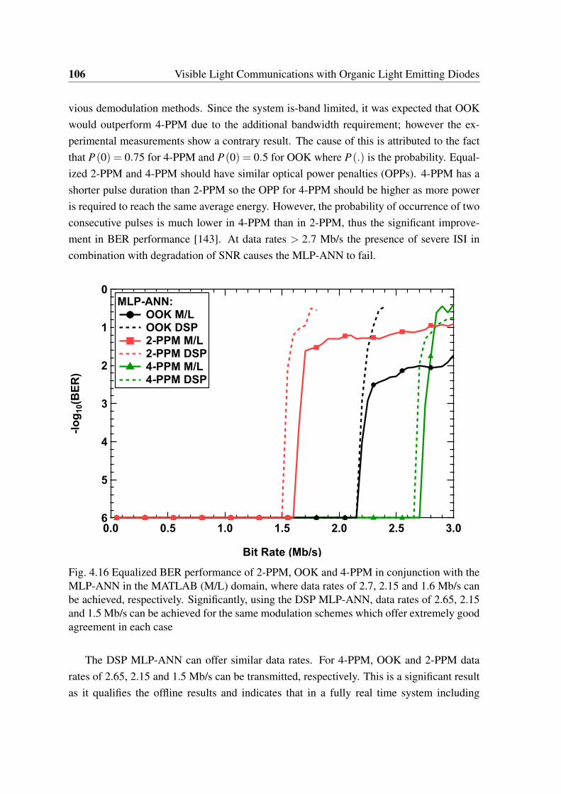
106 Visible Light Communications with Organic Light Emitting Diodes
vious demodulation methods. Since the system is-band limited, it was expected that OOKwould outperform 4-PPM due to the additional bandwidth requirement; however the ex-perimental measurements show a contrary result. The cause of this is attributed to the factthat P(0) = 0.75 for 4-PPM and P(0) = 0.5 for OOK where P(.) is the probability. Equal-ized 2-PPM and 4-PPM should have similar optical power penalties (OPPs). 4-PPM has ashorter pulse duration than 2-PPM so the OPP for 4-PPM should be higher as more poweris required to reach the same average energy. However, the probability of occurrence of twoconsecutive pulses is much lower in 4-PPM than in 2-PPM, thus the significant improve-ment in BER performance [143]. At data rates > 2.7 Mb/s the presence of severe ISI incombination with degradation of SNR causes the MLP-ANN to fail.
6
5
4
3
2
1
0
-lo
g1
0(B
ER
)
3.02.52.01.51.00.50.0
Bit Rate (Mb/s)
MLP-ANN: OOK M/L OOK DSP 2-PPM M/L 2-PPM DSP 4-PPM M/L 4-PPM DSP
Fig. 4.16 Equalized BER performance of 2-PPM, OOK and 4-PPM in conjunction with theMLP-ANN in the MATLAB (M/L) domain, where data rates of 2.7, 2.15 and 1.6 Mb/s canbe achieved, respectively. Significantly, using the DSP MLP-ANN, data rates of 2.65, 2.15and 1.5 Mb/s can be achieved for the same modulation schemes which offer extremely goodagreement in each case
The DSP MLP-ANN can offer similar data rates. For 4-PPM, OOK and 2-PPM datarates of 2.65, 2.15 and 1.5 Mb/s can be transmitted, respectively. This is a significant resultas it qualifies the offline results and indicates that in a fully real time system including

4.4 Summary 107
clock recovery it would be feasible to achieve Mb/s data rates. The difference betweeneach case is 0.05, 0 and 0.1 Mb/s for 4-PPM, OOK and 2-PPM, respectively which in termsof percentage is 1.85%, 0% and 6.25%, indicating a very small difference in each case. Itshould also be noted that in each case the MATLAB MLP-ANN outperforms the DSP basedMLP-ANN.
4.4 Summary
In this chapter the optoelectronic characteristics of the SMOLED are outlined. Subse-quently, a 2.7 Mb/s VLC link with the SMOLED as transmitter and a Si PD as receiverhas been examined using an ANN equalizer in both offline and online (2.65 Mb/s) configu-rations. In comparison to previously reported works, the record data rate has been improvedby two fold, from 1.4 Mb/s [63] up to 2.7 Mb/s for any state-of-the art organic VLC sys-tem. In terms of pulse modulation the improvement is four fold from 550 kb/s [59] to 2.15Mb/s (for OOK) and five times from 550 kb/s to 2.7 Mb/s (for 4-PPM). The reason forthis is due to the significantly reduced probability of occurrence of two consecutive pulsesin 4-PPM in comparison to OOK. Furthermore, it is the first time online filtering has beendemonstrated for any VLC system, offering good agreement with the offline results.


Chapter 5
Visible Light Communications withOrganic Photodetectors
5.1 Introduction
This chapter will concentrate on VLC systems with an inorganic WPLED as the transmitterwith an OPD receiver. The OPD under test is a P3HT:PCBM device with P3HT inter-layer. It is a custom device that was manufactured under collaboration by Siemens AG,Corporate Technology. The external quantum efficiency of the P3HT:PCBM blend is out-lined in Fig. 5.1, while in Fig. 5.2 the responsivity is shown in comparison to the ThorLabsPDA36A-EC Si PD.
From Fig. 5.2 it is clear that the OPD has some significant advantages over Si PDs.Firstly, the large ∼ 2 eV band gap energy means that the cut-off wavelength is around 620nm (red wavelengths) and no IR noise is absorbed. Secondly, the OPD responsivity is muchhigher (more than twice in some cases) than the Si PD at a significantly lower bias voltage(> 20 V) across the entire active region. This is important for VLC systems, especiallyconsidering the common reliance on GaN (blue) based WPLEDs that often require bluefiltering to recover their fast transient responses. The peak wavelength in such LEDs istypically 445 nm (see Fig. 1.4 in Chapter 1), which corresponds to a responsivity of ∼0.1 A/W for Si PDs and 0.25 A/W for the OPD under test meaning a better quality signal isobtained at the receiver. The major disadvantage is that the red wavelengths are not absorbedas mentioned which means that OVLC WDM capacity is reduced considering that a red lightis required to contribute to the white balance and no information could be recovered fromthese wavelengths.
As reported in [61] the OPD bandwidth is heavily dependent on the incident light density

110 Visible Light Communications with Organic Photodetectors
Fig. 5.1 EQE of the P3HT:PCBM OPD under test
Fig. 5.2 Responsivity of the P3HT:PCBM OPD under test in comparison to a Si PD

5.2 Communications Performance 111
(W/m2) due to traps at the interface. Under a high light intensity (> 300 µW/cm2) thenumber of charge carriers generated exceeds the number of traps at the interface and thetime constant of the plate capacitance controls the overall cut-off frequency as in Si PDs.Conversely, at low light intensities the number of traps exceeds the number of charge carriersmeaning that the BW is controlled by the time constant of the interface traps and this canbe illustrated in the bode plot of Fig. 5.3. The OPD is tested with a GaN WPLED as thetransmitter, which has a BW that is around one order of magnitude higher than the organicdevices (∼ 4 MHz); ensuring that the equalizers under test are extending the operationalrange of the organic devices.
-18
-15
-12
-9
-6
-3
0
20
log
10(U
/U0)
(dB
)
104
105
106
Frequency (Hz)
56 kHz
10 mW/cm2
76 kHz
50 mW/cm2
160 kHz
300 mW/cm2
110 kHz
270 mW/cm2
Fig. 5.3 OPD BWs for four light densities, varying from 10 to 300 µWcm−2 corresponds toBWs ranging between 56−−160 kHz, giving ∼ 100 kHz range
5.2 Communications Performance
OPDs are not expected to replace Si PDs in the near future in optical communications due totheir strong market position and wide user base. On the other hand, OPDs can be of interestfor applications where Si PDs are not suitable and therefore are an exciting technology forthe future, also considering the significant cost reduction offered by spray-coating at room
112 Visible Light Communications with Organic Photodetectors
temperature. Due to the low charge carrier mobility in organic semiconductors which areorders of magnitude lower than in Si, the BWs of OPDs are usually much lower than theBWs of Si devices; which is a major challenge.
The OPDs under test are produced under collaboration by Siemens AG Corporate Tech-nology and are based on the BHJ principle [96]. Four diodes with 1 cm2 active area eachare fabricated on a single 5× 5 cm2 transparent glass substrate as previously illustrated inFig. 2.14 and Fig. 2.15 in Chapter 2.
The thin film (∼500 nm) organic semiconductor layer, a blend of P3HT as the donormaterial and PCBM as the acceptor material, is deposited by spray-coating from a xylenesolution as in [54], which leads to extremely low material cost devices (∼£0.17 cm−2).This simple fabrication technique is extremely attractive for VLC systems. The OPD BWis dynamic and dependent on the incident light intensity, as reported in [61]. In high lightdensities, the number of charge carriers is greater than the number of interface traps andtherefore the BW is proportional to the time constant of the plate capacitance. Conversely inlow light densities, the number of interface traps outnumbers the number of charge carriersso the BW is proportional to the traps time constant.
Further, the OPD is also attractive for VLC systems due to its superior responsivitycompared to Si photodetectors in the visible range under a much smaller reverse bias asshown in Fig. 5.2. It also has a sharp cut-off wavelength at ∼620 nm due to the larger bandgap of P3HT (∼2 eV) in comparison to Si (∼1.16 eV). It should be noted that a band gapof 2 eV is relatively high and has a cut-off wavelength around 620 nm (red wavelengths)which could be a problem for VLC applications that take advantage of wavelength divisionmultiplexing (WDM). The cut-off wavelength can be shifted to the NIR region by replacingP3HT in the BHJ blend with a low band gap material such as PCPDTBT as in [144, 145].
In this chapter BER measurements are made by varying the light densities between 10and 300 µW/cm2; obtaining a BW ranging between ∼ 50− 160 kHz. Furthermore, bothOOK and 4-PPM are investigated. 2-PPM is not examined due to the fact that it has ahigher spectral content around the DC and low frequencies regions while having the sameBW requirements as 4-PPM. No higher orders of PPM are investigated due to the significantadditional BW requirements as mentioned in the previous chapter. At the receiver an ANNequalizer is required to recover the data as in [59] since the required high data rates aremuch higher than the system BW.
5.2.1 Test Setup and Artificial Neural Network
The test setup is shown in Fig. 5.4. The PRBS in the OOK data format is generated inMATLAB and translated into the 4-PPM code. The data is output by a Tektronix AFG3022B
5.2 Communications Performance 113
function generation controlled by LabVIEW (LV in Fig. 5.4) and buffered by a NAND gatewith a high output impedance, then mixed with a DC level prior to intensity modulationof the LED (Philips Luxeon Rebel, BW 4.4 MHz). The white light is transmitted over thelinearly attenuating line-of-sight channel h as given by [17]:
h(0) =Ad2 R0 (θ)cos(ϕ) (5.1)
where A is the OPD active area (1 cm2), d is the distance between the transmitter (LED) andreceiver (OPD), θ is the angle of light emission, ϕ is the angle of incidence and R0 is theLambertian radiation pattern of the LED, given by [17]:
R0 (θ) =m+1
2πcos(ϕ)m (5.2)
where m is the Lambertian order.
At the receiver, the output of the photodetector is passed through an Analog DevicesAD8015 (noise current density 2.4 pA Hz−1/2) transimpedance amplifier the output ofwhich is acquired by an Agilent DSO9254A oscilloscope.
The OPD was reverse biased at -5 V as in [61] using an Agilent 3631A controlled byLabVIEW. Then light was applied to the OPD through the transparent anode electrode. Theapplied light density was measured using a ∼1 cm diameter thermopile disk (14BT, LaserInstrumentation Ltd). In order to gain insight into the OPD performance under differentlight densities, the applied light intensity was varied by varying the transmission (LED-OPD) distance. Incident light densities of 10, 50, 270 and 300 µW/cm2 were generated,and correspond to measured BWs of 56, 76, 110 and 160 kHz, respectively, as illustratedin Fig. 5.3. The BW difference between the lowest and highest light density is ∼100 kHz,which is a significant difference.
OOK is the most common modulation scheme for VLC systems due to its ease of im-plementation and BW efficiency [59]. Data is inferred by the presence or absence of a pulseof energy in the symbol period, see [108, 111]. Conversely PPM is the most power efficientmodulation scheme, requiring half the power of OOK at the expense of a two-fold increasein BW requirement that follows [115]:
PPPM
POOK=
√2
L log2 L(5.3)
where L is the order of PPM. This comes at the cost of decreased BW efficiency, following

114 Visible Light Communications with Organic Photodetectors
LV
VOLED
VPDLED
OPD TIA
Data
Received Data
Fig. 5.4 Schematic system block diagram
[115]:
BWL−PPM =LRb
log2 L(5.4)
where Rb is the bit rate. The spectral signature of 4-PPM contains little or no DC and lowfrequency components thus is ideal for reducing the high-pass filter induced BLW phenom-ena that occurs in indoor optical wireless communication links [59]. Soft demodulation canalso be used with 4-PPM, offering an electrical SNR gain of more than 1.5 dB in the pres-ence of signal distortion. Hence, threshold detection is not considered here for 4-PPM sinceit will yield an inferior result [115].
DMT is a popular option for increasing data rates in VLC systems and extremely highdata rates have been demonstrated. In order to really maximize the bandwidth of such aDMT system three equalizers are required; a pre-equalizer, a time domain equalizer anda post-equalizer. Each of these equalizers requires knowledge of the system and channelresponses (as stated in [146]). So far no widely accepted feedback channel has been usedin VLC systems and therefore such as a system is not currently preferable as it may not beviable in the future.
Instead, a high performance equalizer such as the ANN can be used that does not requireany knowledge of the channel because it acquires this information from a training sequencethat consists of a known header file that is transmitted before the useful information. TheMLP ANN is selected due to its superior performance in symbol error rate to transversallinear equalizers [125]. In theory, the MLP is not the optimal classifier, the DF or RBFANNs should outperform the MLP, however these configurations have significantly highercomputational intensity and complexity for only a slight increase in data rate [142]. TheMLP consists of three layers; an input layer x, a hidden layer and an output layer y with
5.3 Results 115
a single node. The N-input layer is the equivalent of an N-tap delay line in conventionalfilters; the number of nodes in the hidden layer is also made equal to N and is where theprocessing occurs. The output of the MLP is given by:
y = f
(b+∑
iwixi
)(5.5)
where i = 0, . . . , N if a bias b exists and i = 1, . . . , N otherwise. The filter weights aregiven by wi and are adjusted during the ANN training in order to find the correct coefficientsto map the system response.
The ANN is trained by the Levenberg-Marquardt back propagation algorithm with anadaptive learning rate [127], which is supervised training that works on the basis of mini-mizing the error cost function E of a known bit sequence at the receiver and the transmitteddata as follows [124]:
E (n) = |y(n)−d (n)|2 (5.6)
where d is the desired sample and y is the received sample. The back propagation algorithmupdates the weights as follows [124]:
wi j (n+1) = wi j (n)−η∂E (n)
∂wi j (n)(5.7)
Once the ANN is fully trained it can be used to correct the received data.The ANN is capable of generalizing, which is another advantage over linear equalizers.
This means that if the sequence contains transitions that are unknown to the equalizer due tonot being present in the training sequence, the ANN has a higher probability of recoveringthe data than any other linear equalizer [124]. The downside of this is that an excessivenumber of neurons tend to lead to over-fitting, a big problem with ANNs. Therefore it iscrucial to select the correct number of neurons for the system. The ANN is implemented inMATLAB.
5.3 Results
In Fig. 5.5 the BER performance for OOK using both threshold detection (denoted T/H)and the ANN equalizer is shown in high light density conditions with 160 kHz system BW.Furthermore the performance of 4-PPM with soft demodulation and the ANN equalizer isalso shown. First considering the unequalized case, data rates of 500 and 300 kb/s can be

116 Visible Light Communications with Organic Photodetectors
achieved with 4-PPM and OOK, respectively (1000 and 300 kHz BW requirement, respec-tively), showing that 4-PPM significantly outperforms OOK by offering ∼66% additionaldata rate.
6
5
4
3
2
1
0
-lo
g1
0(B
ER
)
43210
Bit Rate (Mb/s)
OOK T/H 4-PPM Soft OOK ANN 4-PPM ANN
Fig. 5.5 BER performance for OOK and 4-PPM with and without ANN equalization
The reason for this is attributed to the fact that soft demodulation depends on the signalgradient. As opposed to threshold detection, where the bit levels are assigned with refer-ence to an average value, soft demodulation reshapes the incoming signal into an L columnmatrix. The highest value is assigned a 1-level and the rest are assigned 0-levels. Failure ofsoft decoded 4-PPM is therefore caused by the rapid transmission of alternative states wherethe transient response of the OPD is not sufficient and the signal gradient cannot becomenegative to be assigned a 0-level.
Considering the ANN equalizer performance, 4-PPM and OOK can offer 3.75 and 2.8Mb/s, respectively. As with the unequalized case, 4-PPM significantly outperforms OOK.Over ∼1 Mb/s extra data rate can be recovered with 4-PPM than OOK. The BW require-ments are 7.5 and 2.8 MHz, respectively. The reason for the additional performance is thatthe ANN can easily differentiate between single pulses of energy followed by long streamsof 0-levels in a highly multipath induced ISI environment. While in OOK each level is

5.3 Results 117
equiprobable and there is therefore too much signal distortion in order to accurately esti-mate of the system response that is required for the ANN to undo the ISI effect.
It is established that 4-PPM outperforms OOK in high light density conditions. There-fore now the BER performance of 4-PPM with the ANN equalizer is investigated over thefour BWs (56, 76, 110 and 160 kHz) that are obtained by using four different light densities(10, 50, 270 and 300 µW/cm2), see Fig. 5.6. The case of the 160 kHz BW has alreadybeen covered and can support 3.75 Mb/s. Data rates up to 2.4, 1.45 and 1.15 Mb/s can besupported for the BW in the descending order.
6
5
4
3
2
1
0
-lo
g10(B
ER
)
43210
Bit Rate (Mb/s)
4-PPM BER: 56 kHz 76 kHz 110 kHz 160 kHz
Fig. 5.6 BER performance of 4-PPM across the system with varying light density - in eachcase, over 1 Mb/s can be supported
Each of the system BWs are separated by between ∼ 20−40 kHz and the performancedecreases proportionally to the difference between them as expected. For example, thereis a drop of 1.45 Mb/s between the 160 and 110 kHz cases (40 kHz difference) which issignificant. Furthermore there are drops of ∼1 Mb/s between the 110 and 76 kHz cases (34kHz difference) while between 76 and 56 kHz the drop in data rate is only 0.3 Mb/s (20kHz). Therefore the performance is clearly related to the decrease in SNR with decreasinglight density and the increasing influence of ISI, thus making the data unrecoverable. Never-theless, data rates >1 Mb/s can be recovered across the entire system, which is an important
118 Visible Light Communications with Organic Photodetectors
result for OPD-VLC systems as MHz devices are starting to emerge [147] that could usethis technology in order to provide high speed and low cost VLC systems.
5.4 Multiple-Input Multiple-Output
5.5 Introduction
MIMO systems based on the concept of channel matrix inversion [148] are an excellentway to increase the aggregate bit rates in visible light communications (VLC) systems. Asa result they have garnered a significant amount of interest in the research community withmany different methods of implementing the MIMO technique being proposed [148–153].For example, different modulation schemes are reported in [149] and [152] while [151]offers a spatially diverse scheme where only one transmitter is active at any given time.Furthermore, based on the simulation results in [150] there is a strong claim that a compleximaging receiver is required in order to receive an error free link [148–150] due to an ill-conditioned channel matrix rank.
This is not the case, however and here verification that it is possible to recover a 4× 4MIMO link without employing a complex imaging receiver is presented. A data rate of 1.8Mb/s is achieved using this technique.
While the benefits of using WPLEDs for VLC and SSL are well known (high outputpower, bandwidths of several MHz [26]), using OPDs as the receiver for VLC systems isa subject in its infancy. Single-input single-output (SISO) links have been covered in theprevious chapters and an ANN equalizer has been used to increase the data rate to 3.75Mb/s from a system bandwidth of 160 kHz. In this section, a MIMO system based on fourindividual commercial WPLEDs and four OPDs that are mounted on the same substrate.
The OPD used is based on the BHJ concept [96], which is an interpenetrated blendof electron donor and electron acceptor, as opposed to the common p-n junction that SiPDs utilizes. It was manufactured by Siemens AG Corporate Technology by the spraydeposition technique as reported in [54]. When comparing organic technologies with their Sicounterparts, the real advantage is the price. The total bill of materials for the P3HT:PCBMsystem implemented here is ∼£0.17 cm−2, which is very inexpensive. The materials canbe processed into a solution that can be sprayed onto the substrate, allowing very low costand straightforward manufacturing. Besides spray coating there are other ways to producedevices, see [154] for further details on a number of methods. Additionally, the OPD BWis dynamic [61], and its performance is controlled by the incident light intensity. Under ahigh light intensity (> 300 µW/cm2) the number of charge carriers generated is greater than
5.6 MIMO Theory 119
the number of traps at the interface meaning that the time constant of the plate capacitancecontrols the cut-off frequency as in Si PDs. Conversely at low light intensities the numberof traps is greater than the number of charge carriers, meaning that the BW is controlled bythe time constant of the interface traps.
A further advantage of the OPD under test is that is has four independent diodes spaced1.2 cm apart each with 1 cm2 photoactive area meaning that 4× 4 (4-transmitters and 4-receivers) MIMO is a natural progression on SISO links. No additional electronics or pho-todetectors are required at the receiver as in Si based MIMO, and therefore there is noadditional cost. Since there are four diodes on the OPD substrate, 4×4 MIMO is investi-gated in this Chapter. While the theory of demodulating a MIMO link is extremely simple(outlined mathematically in Section 5.6), a series of pilot tones are transmitted from the firsttransmitter to all receivers in order to find the channel response (while keeping the rest of thetransmitters off) and repeating for each transmitter. A matrix of channel coefficients is pro-duced, inverted and multiplied with the received data in order to find the transmitted data.In practice this is a significant challenge for bandlimited systems due to the ISI induceddistortion of the reference signals [59] that make up the channel matrix coefficients.
MIMO systems are typically implemented in the radio frequency domain where a mul-tipath environment is inherent. There are many reports of using an ANN to find the channelresponse [155, 156]; however to the best of the author’s knowledge there are no reports ofapplying an ANN at all in VLC MIMO systems. This is because they are mostly used forcorrecting ISI at the receiver. One cause of ISI is transmitting data outside of the modulationBW, which is not a problem that is observed in MIMO systems explicitly, since the qualityof the channel coefficient matrix has more impact in recovering the data than the ISI. In thisChapter it is demonstrated that not only is it possible to implement the ANN to equalize thereceived signal but it is also possible to use the ANN to set a new record data rate basedupon the ANN for a large coverage area beneath the transmitter array.
5.6 MIMO Theory
The concept of MIMO is outlined in Fig. 5.7. Over the next few subsections the transmitter,channel and receiver are outlined.
5.6.1 Transmitters
A pseudorandom binary sequence is generated and shaped into an OOK signal in MAT-LAB. Two arbitrary function generators (AFGs) with a peak-to-peak output voltage of 5 V
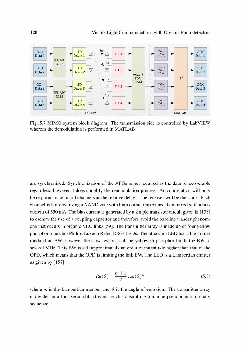
120 Visible Light Communications with Organic Photodetectors
LabVIEW MATLAB
OOK Data 1
LED Driver 1
LED Driver 2
LED Driver 3
LED Driver 4
OOK Data 2
OOK Data 3
OOK Data 4
TIA 1
TIA 2
TIA 3
TIA 4
Agilent DSO
9254AH-1
OOK Data 1
OOK Data 2
OOK Data 3
OOK Data 4
TEK AFG 3022
TEK AFG 3252
h11
h12
h13
h14
Fig. 5.7 MIMO system block diagram: The transmission side is controlled by LabVIEWwhereas the demodulation is performed in MATLAB
are synchronized. Synchronization of the AFGs is not required as the data is recoverableregardless; however it does simplify the demodulation process. Autocorrelation will onlybe required once for all channels as the relative delay at the receiver will be the same. Eachchannel is buffered using a NAND gate with high output impedance then mixed with a biascurrent of 350 mA. The bias current is generated by a simple transistor circuit given in [138]to eschew the use of a coupling capacitor and therefore avoid the baseline wander phenom-ena that occurs in organic VLC links [59]. The transmitter array is made up of four yellowphosphor blue chip Philips Luxeon Rebel DS64 LEDs. The blue chip LED has a high ordermodulation BW; however the slow response of the yellowish phosphor limits the BW toseveral MHz. This BW is still approximately an order of magnitude higher than that of theOPD, which means that the OPD is limiting the link BW. The LED is a Lambertian emitteras given by [157]:
R0 (θ) =m+1
2cos(θ)m (5.8)
where m is the Lambertian number and θ is the angle of emission. The transmitter arrayis divided into four serial data streams, each transmitting a unique pseudorandom binarysequence.
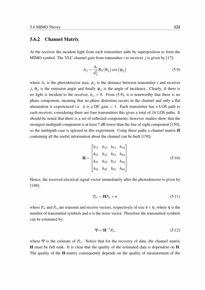
5.6 MIMO Theory 121
5.6.2 Channel Matrix
At the receiver the incident light from each transmitter adds by superposition to form theMIMO symbol. The VLC channel gain from transmitter i to receiver j is given by [17]:
hi j =Ar
d2i j
R0(θi j)
cos(ϕi j)
(5.9)
where Ar is the photodetector area, di j is the distance between transmitter i and receiverj, θi j is the emission angle and finally ϕi j is the angle of incidence. Clearly, if there isno light is incident to the receiver, hi j = 0. From (5.9), it is noteworthy that there is nophase component, meaning that no phase distortion occurs in the channel and only a flatattenuation is experienced i.e. it is a DC gain < 1. Each transmitter has a LOS path toeach receiver; considering there are four transmitters this gives a total of 16 LOS paths. Itshould be noted that there is a set of reflected components; however studies show that thestrongest multipath component is at least 7 dB lower than the line of sight component [150],so the multipath case is ignored in this experiment. Using these paths a channel matrix Hcontaining all the useful information about the channel can be built [150]:
H =
h11 h12 h13 h14
h21 h22 h23 h24
h31 h32 h33 h34
h41 h42 h43 h44
(5.10)
Hence, the received electrical signal vector immediately after the photodetector is given by[148]:
Prx = HPtx +n (5.11)
where Ptx and Prx are transmit and receive vectors, respectively of size 4×η , where η is thenumber of transmitted symbols and n is the noise vector. Therefore the transmitted symbolscan be estimated by:
Ψ = H−1Prx (5.12)
where Ψ is the estimate of Ptx. Notice that for the recovery of data, the channel matrixH must be full rank. It is clear that the quality of the estimated data is dependent on H.The quality of the H-matrix consequently depends on the quality of measurement of the

122 Visible Light Communications with Organic Photodetectors
individual channel coefficients. The channel coefficient hi j is controlled by d2i j as (θi j and
ϕi j change as a function of modifying d2i j) while Ar is a constant. A further consideration is
that Ψ is dependent on the noise n. So far, no studies have been carried out on the impact ofthe noise on H. Tracking d2
i j in real time to build the H-matrix would be very problematicexperimentally as it would involve a feedback channel - something not implemented in thiswork.
A far more simplistic approach is a histogram method. One LED transmits data overthe channel while the remaining receivers are not active. The DC level is removed fromthe signal and the electrical signal levels are found. Recalling Vpp = 5 V, removing the DCcorresponds to signal levels of ±2.5 V. Therefore it is easy to rapidly find the DC gain ofthe given channel with a simple division. The method is then repeated for each LED in thetransmitter to build H - see Fig. 5.8 and 5.9 for an example.
There is a drawback to this method; when transmitting outside the BW of the OPD,the influence of ISI will be significant, degrading the peaks of the histogram meaning theestimate of the signal will not be optimal. In the presence of severe ISI the histogram will failcompletely since the histogram will not find any distinction between the two levels. In thistest, the histogram measurement is only performed once for the each channel because thereceiver is not moving continuously. For a real time measurement, H would be periodicallyupdated.
5.6.3 Receiver
The x−z and x−y plane geometries are illustrated in Fig. 5.10(a)and (b), respectively whereFig. 5.10(a) demonstrates the previously outlined concepts and Fig. 5.10(b) shows the re-ceiver plane geometry. Only one quarter of the possible area is tested, since the performanceis expected to be symmetrical around the centre. This area is separated into nine sections of5 cm2 (S1:S9) to give an outline of the position-dependent performance. However beforethe performance is analysed, it is necessary to characterize the OPD under test.
As mentioned, there are four diodes on the substrate, as illustrated in Fig. 5.11, whichalso shows the spatial characteristics of the OPD. The distance di j between the transmitterand receiver is set to maximize the light density while maintaining full coverage by all otherLEDs. Within the receiving plane, the maximum light density is found directly beneath oneof the LEDs, i.e. section S3, which corresponds to a light density of > 300 µW/cm2 anda BW of 177 kHz. The minimum is found in the centre of the receiving plane; section S7where the light density is ∼ 300 µW/cm2 and the BW is 133 kHz, see Fig. 5.12.
The light density is measured with a thermopile of area 12 cm2 and the bandwidth isfound by performing a fast Fourier transform on a short pulse (duration 1 µs with rise and
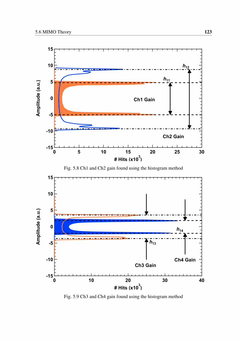
5.6 MIMO Theory 123
-15
-10
-5
0
5
10
15
Am
pli
tud
e (
a.u
.)
302520151050
# Hits (x103)
Ch1 Gain
Ch2 Gain
h11
h12
Fig. 5.8 Ch1 and Ch2 gain found using the histogram method
-15
-10
-5
0
5
10
15
Am
pli
tud
e (
a.u
.)
403020100
# Hits (x103)
Ch3 GainCh4 Gain
h13
h14
Fig. 5.9 Ch3 and Ch4 gain found using the histogram method

124 Visible Light Communications with Organic Photodetectors
LED
x
z
(a)
5 cm
5 cm
x
y
S1 S2
S4 S5
S7 S8
10 cm
10 cm
S6
S3
S9
(b)
OPD
10 cm
Fig. 5.10 (a) x− y plane and (b) x− y plane: the receiver plane divided into sections S1-S9for BER measurements
fall times of 2 ns) transmitted over all 4-LEDs. The BW decreases from a maximum of 177kHz to 133 kHz as the receiver approaches the centre of the receiving plane. This differenceis quite large in relation to the magnitude of the BW. However, in terms of a MIMO signalat the centre of the receiving plane the contribution from each LED is much greater, so it isexpected that this position will offer the largest data rate. Normally it would be predictedthat the largest BW would offer the greatest data rate, yet since the bit rate will exceedthe BW in all sections, ISI will distort the signals significantly thus causing the histogrammethod to fail.
The data is transferred in each section and sampled with an Agilent DSO9254A real timescope controlled by LabVIEW. In the histogram method, data demodulation and estimationare all performed in MATLAB. While an FPGA could have been implemented for a realtime result, there was a strong indication from the literature that the experiment would notprove conclusive without an imaging lens. Therefore to avoid the costly development timeMATLAB is selected for this first demonstration.

5.6 MIMO Theory 125
1 cm
1 cm
1.2 cm
Fig. 5.11 Bottom view photograph of the OPD showing the spatial characteristics
-40
-30
-20
-10
0
No
rmal
ized
Am
plit
ud
e (d
B)
104
2 3 4 5 6 7 8 9
105
2 3 4 5 6 7 8 9
106
Frequency (Hz)
S7: 133 kHz
S3: 177 kHz
Fig. 5.12 BW in the highest and lowest light densities on the receiving plane
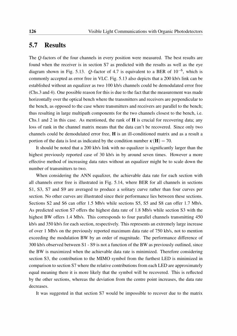
126 Visible Light Communications with Organic Photodetectors
5.7 Results
The Q-factors of the four channels in every position were measured. The best results arefound when the receiver is in section S7 as predicted with the results as well as the eyediagram shown in Fig. 5.13. Q–factor of 4.7 is equivalent to a BER of 10−6, which iscommonly accepted as error free in VLC. Fig. 5.13 also depicts that a 200 kb/s link can beestablished without an equalizer as two 100 kb/s channels could be demodulated error free(Chs.3 and 4). One possible reason for this is due to the fact that the measurement was madehorizontally over the optical bench where the transmitters and receivers are perpendicular tothe bench, as opposed to the case where transmitters and receivers are parallel to the bench;thus resulting in large multipath components for the two channels closest to the bench, i.e.Chs.1 and 2 in this case. As mentioned, the rank of H is crucial for recovering data; anyloss of rank in the channel matrix means that the data can’t be recovered. Since only twochannels could be demodulated error free, H is an ill-conditioned matrix and as a result aportion of the data is lost as indicated by the condition number κ (H) = 70.
It should be noted that a 200 kb/s link with no equalizer is significantly larger than thehighest previously reported case of 30 kb/s in by around seven times. However a moreeffective method of increasing data rates without an equalizer might be to scale down thenumber of transmitters to two.
When considering the ANN equalizer, the achievable data rate for each section withall channels error free is illustrated in Fig. 5.14, where BER for all channels in sectionsS1, S3, S7 and S9 are averaged to produce a solitary curve rather than four curves persection. No other curves are illustrated since their performance lies between these sections.Sections S2 and S6 can offer 1.5 Mb/s while sections S5, S5 and S8 can offer 1.7 Mb/s.As predicted section S7 offers the highest data rate of 1.8 Mb/s while section S3 with thehighest BW offers 1.4 Mb/s. This corresponds to four parallel channels transmitting 450kb/s and 350 kb/s for each section, respectively. This represents an extremely large increaseof over 1 Mb/s on the previously reported maximum data rate of 750 kb/s, not to mentionexceeding the modulation BW by an order of magnitude. The performance difference of300 kb/s observed between S1 - S9 is not a function of the BW as previously outlined, sincethe BW is maximized when the achievable data rate is minimized. Therefore consideringsection S3, the contribution to the MIMO symbol from the furthest LED is minimized incomparison to section S7 where the relative contributions from each LED are approximatelyequal meaning there it is more likely that the symbol will be recovered. This is reflectedby the other sections, whereas the deviation from the centre point increases, the data ratedecreases.
It was suggested in that section S7 would be impossible to recover due to the matrix
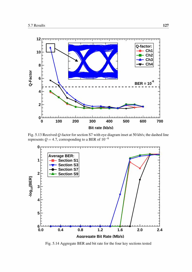
5.7 Results 127
12
10
8
6
4
2
0
Q-F
acto
r
7006005004003002001000
Bit rate (kb/s)
BER = 10-6
Q-factor: Ch1 Ch2 Ch3 Ch4
Fig. 5.13 Received Q-factor for section S7 with eye diagram inset at 50 kb/s; the dashed linerepresents Q = 4.7, corresponding to a BER of 10−6
6
5
4
3
2
1
0
-lo
g10
(BE
R)
2.42.01.61.20.80.40.0
Aggregate Bit Rate (Mb/s)
Average BER: Section S1 Section S3 Section S7 Section S9
Fig. 5.14 Aggregate BER and bit rate for the four key sections tested
128 Visible Light Communications with Organic Photodetectors
correlation; however the data could be recovered in these tests. While in theory, if thechannel paths and transmission power are identical, the matrix will correlate. In practice,however this situation is extremely unlikely to occur due to the combination of the additivewhite Gaussian noise (AGWN) that exists in the system plus the fact that the LEDs are notperfectly identical so will have slightly different output characteristics.
In the worst case scenario, 1.4 Mb/s could be achieved, which still denotes a sizeableimprovement as mentioned. This result is important not only for this reason, but because itmeans that data can be demodulated at all positions on the receiving plane indicating thatMIMO is a valid technique for future organic VLC systems. It is important not to forgetthat in all cases an ANN was required to equalize the errors induced throughout the system.Without the ANN, only 100 kb/s could be transmitted over two channels. While not closeto the 1.8 Mb/s reported above, in comparison to other unequalized LED to OPD links, thisis still an increase over previously published work.
5.8 Conclusion
In this Chapter an experimental demonstration of a MIMO system for an organic VLCsystem is presented. Whilst providing this demonstration, the record data rate of 750 kb/sfor VLC systems with Si LEDs and OPDs as transmitter and receiver, respectively hasbeen well broken, as 1.8 Mb/s can now be transmitted, which is a significant step in theprogression of organic VLC. The major challenge in this Chapter was to overcome thepoorly conditioned matrix to recover the data at the receiver. In order to achieve this, anANN equalizer was proposed to map the input-output sequence and correct the errors, whichresulted in achieving extremely high data rates. The feasibility of VLC-MIMO without theuse of an imaging receiver was demonstrated for the first time.
Future work on this topic considers what is missing from this preliminary experiment.Firstly, an FPGA development is required to provide a real time link which can fully ex-plore the influence of white noise on H, which will allow the derivation of new theory onthe recovery of MIMO symbols for VLC links. Secondly, in order to provide a full scaledemonstration, the number of OLEDs needs to be scaled up to provide full illuminationof a small room. It would be expected that the link has the same performance as in thesmall scale link that is presented here, and so far a full scale demonstration has not beendemonstrated.
Chapter 6
Visible Light Communications with AllOrganic Optoelectronic Components
6.1 Introduction
To date a VLC link employing exclusively organic optoelectronic components has not beendemonstrated, despite enormous interest in both the organic based devices [67, 70, 100]and VLC [158–160] in the research community. This can be attributed to two main rea-sons; firstly there is a lack of commercially available organic devices - just a handful ofSMOLEDs are available to purchase off-the-shelf while no OPDs are commercially avail-able and must be custom made. Secondly, OVLC has only recently emerged as a serioustopic for research and all of the reports so far have focused on either the transmitter [160]or receiver [158], as opposed to a full system evaluation. In spite of this it is necessary toperform such an evaluation because organics have outstanding properties that are ideallysuited to the VLC domain. For instance, they can be processed into mechanically flexible,arbitrarily shaped panels with large photoactive areas. Such devices are processed by solu-tion based processing at room temperature offering a real cost reduction; unlike inorganicswhich must be processed with epitaxial methods resulting in brittle crystals that do not scalewell. Further, by careful selection of the semiconducting polymer it is possible to tune theemission or absorption wavelength to visible light as polymers and small molecules withband gap energies of 1 - 4 eV are abundant.
Even considering a forecasted market value of ∼£200 billion by 2027 [60], it is notanticipated that organic devices will become dominant over inorganics in optical communi-cations and there are several reasons why. Firstly, a widespread infrastructure already existsfor inorganics, which is well established and maintained. Secondly inorganic devices can be
130 Visible Light Communications with All Organic Optoelectronic Components
easily and homogenously produced without defects or impurities. On the other hand, organ-ics have the potential for applications in areas where inorganics are not perfectly suited orno optimized infrastructure exists. This could be in the screens and chassis of future mobiledevices for device-to-device communications where OLEDs have already started appearing.Finally and most importantly, charge transport characteristics are orders of magnitude lowerin organics and the direct result of this is that the bandwidths available for organics are inthe kHz region (in comparison to MHz for inorganics). This is an open and timely challengefor OVLC links because the bandwidth is the most important factor for increasing capacity.The other is the SNR, which has an upper bound limit caused by the lighting requirementsin VLC (max ∼400 lux) and also the quantum efficiencies and noise performance of thedevices. However, having a low bandwidth is not necessarily a fatal perturbation for OVLC.In [159] a 10 Mb/s link was achieved using an organic polymer LED with 270 kHz band-width and a least mean squares equalizer. Although this report is a significant landmark forOVLC, a silicon photodetector was used instead of an OPD. Digital equalization techniquesare an attractive option to increase transmission speeds as they restore link performance inthe presence of ISI caused by the bandwidth limitation. The modulation format selected inthis work is OOK due to its simplicity and popularity in the VLC domain [58, 158, 160].Furthermore, OOK is compatible with transversal equalizers such as the MLP ANN whichoffer the best BER performance of any equalizer [142].
Aside from the bandwidth magnitude there is a further challenge in this setup. In [61] adetailed investigation was undertaken that reported OPD bandwidths can vary over severalorders of magnitude from a few kHz to hundreds of kHz according to the incident lightdensity (W/cm2) due to interface charge traps. In high light density conditions, the numberof charge carriers generated exceeds the number of interface traps, and therefore the BW isproportional to the time constant of the plate capacitance as with inorganic detectors (maxbandwidth available ∼150 kHz [97]). Alternatively, in low light density conditions, thenumber of charge traps surpasses the number of charge carriers; so the overall bandwidthis proportional to the time constant of the traps, which varies with the ratio of empty/filledtraps. In this work the worlds’ first OVLC link operating at a link speed > 1 Mb/s is pro-posed and demonstrated. In order to achieve this, the ANN equalizer is required to removethe effect of ISI. Furthermore, by varying the bias current of the OLED, the incident lightdensity is reduced, thus reducing the bandwidth. Three cases are examined; a high (135kHz), medium (100 kHz) and low bandwidth case (65 kHz) in order to find out the limita-tions of such links.

6.2 Organic Optoelectronic Devices 131
6.2 Organic Optoelectronic Devices
In this work the same SMOLED is used as in previous chapters as the transmitter and thesame OPD as the receiver. While specific material details are not available for the OLED, theOPD is based on the bulk heterojunction concept - an interpenetrated blend of electron donorand electron acceptor (P3HT:PCBM) [96], which is dissolved into a solvent and sprayedonto the substrate.
P3HT:PCBM OPDs have higher responsivity than that of silicon detectors across thevisible range whilst requiring a significantly lower reverse bias voltage of ∼3 - 5 V. Fur-thermore, P3HT:PCBM OPDs are infrared blind due to the higher band gap energy of ∼2eV (∼1.1 eV for silicon), which results in a sharp cut-off wavelength of ∼620 nm (∼1100nm for silicon). It should be noted that the 2 eV band gap is relatively high for VLC ap-plications, which would benefit from a longer cut-off wavelength for applications such aswavelength division multiplexing, which can achieved by careful selection of the polymer[145]. On the other hand, as can be inferred from Fig. 6.1 (inset) the majority of the warm-white OLED optical power is absorbed by the OPD under test. The L-I-V is the main featureof Fig. 6.1 and the measured response shows good linearity up to 1 A, which is well beyondthe 540 mA recommended operating limit set by the manufacturer.
In order to make bandwidth measurements and select an appropriate operating point, theDC level is varied between 0.1-0.8 A. The bandwidth of the system under test is shown inFig. 6.2, which varies from 38 kHz to 146 kHz. It should be noted that in order to achieve146 kHz a bias current of up to 0.8 A is required. Reducing the current to ∼0.5 A gives aslightly reduced bandwidth of ∼135 kHz while operating within the recommended region.Three bandwidths (bias currents) are selected for this work; 135 kHz (0.5 A) as the highbandwidth case, 100 kHz (0.35 A) as the mid-range case and 65 kHz (0.175 A) as thelow case. A lower bandwidth was not selected because a symmetrical swing could not beachieved and the AC signal would therefore be clipped at the 0-level.
6.3 Test Setup
The experimental test setup is illustrated by the block diagram in Fig. 6.3. An arbitrary func-tion generator (TEK AFG3022B) is loaded with a 210-1 (PRBS-10) generated in MATLABand passed through a unit height rectangular pulse shaping filter p(t). The rectangular sig-nal is then mixed with a DC current using a bias tee to ensure operation in the linear regionof the transmitter. The DC-biased signal then intensity modulates the OLED. The channelh is a less-than-unity DC gain that is not frequency selective for the required bandwidth in

132 Visible Light Communications with All Organic Optoelectronic Components
5
4
3
2
1
0
Vo
ltag
e (V
)
1.41.21.00.80.60.40.20.0
Bias Current (A)
1.0
0.8
0.6
0.4
0.2
0.0
No
rma
lize
d O
pti
ca
l P
ow
er
(a.u
.)
1.0
0.8
0.6
0.4
0.2
0.0
No
rma
lize
d R
es
po
ns
e
800700600500400
Wavelength (nm)
Maximum safe
operating point
Fig. 6.1 The L-I-V curve of the OLED under test with linear fitting; normalized emissionand absorption spectra of the OLED (blue) and OPD (red) respectively, noting that the vastmajority of optical power is absorbed before the cut-off wavelength
-10
-8
-6
-4
-2
0
20lo
g(U
/U0)
200150100500
Frequency (kHz)
38 kHz
146 kHz
108 kHz
0.8
0.6
0.4
0.2
0.0
IBia
s (A)
Fig. 6.2 Normalized and measured bandwidths of the OPD under test under different currentbias conditions of the OLED, which control the light density
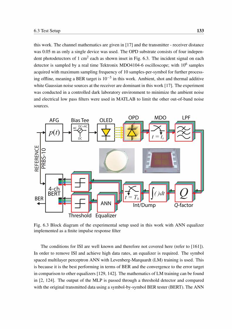
6.3 Test Setup 133
this work. The channel mathematics are given in [17] and the transmitter - receiver distancewas 0.05 m as only a single device was used. The OPD substrate consists of four indepen-dent photodetectors of 1 cm2 each as shown inset in Fig. 6.3. The incident signal on eachdetector is sampled by a real time Tektronix MDO4104-6 oscilloscope; with 106 samplesacquired with maximum sampling frequency of 10 samples-per-symbol for further process-ing offline, meaning a BER target is 10−5 in this work. Ambient, shot and thermal additivewhite Gaussian noise sources at the receiver are dominant in this work [17]. The experimentwas conducted in a controlled dark laboratory environment to minimize the ambient noiseand electrical low pass filters were used in MATLAB to limit the other out-of-band noisesources.
4-chBERT
ANNANNANN
∫( )dtt = Tb ∫( )dtt = Tb ∫( )dtt = Tb
t = tsp(t)
AFG OLED
QQQANN
BER
DC
ACDC+AC
RE
FE
RE
NC
E
t = tst = tst = ts
∫( )dt Qt = Tb
OPD MDO LPFBias Tee
Int/Dump
Equalizer
Q-factor
Threshold
PR
BS
-10
Fig. 6.3 Block diagram of the experimental setup used in this work with ANN equalizerimplemented as a finite impulse response filter
The conditions for ISI are well known and therefore not covered here (refer to [161]).In order to remove ISI and achieve high data rates, an equalizer is required. The symbolspaced multilayer perceptron ANN with Levenberg-Marquardt (LM) training is used. Thisis because it is the best performing in terms of BER and the convergence to the error targetin comparison to other equalizers [129, 142]. The mathematics of LM training can be foundin [2, 124]. The output of the MLP is passed through a threshold detector and comparedwith the original transmitted data using a symbol-by-symbol BER tester (BERT). The ANN
134 Visible Light Communications with All Organic Optoelectronic Components
and BERT are implemented in MATLAB.
6.4 Results
The unequalized BER and Q-factor performance of the link for a range of bandwidth willbe illustrated in descending order followed by the equalized BER performances. Fig. 6.4 il-lustrates the BER envelope for the four diodes without equalization for 135 kHz bandwidth.The BER envelope is produced by analyzing the performance of each of the four diodes andselecting the maximum and minimum at each data rate. The average BER is calculated andused to represent the overall link performance. The average error free (BER= 10−5) achiev-able transmission speed is 350 kb/s without equalization. Considering the BER envelope,the minimum and maximum available speeds are 350 and 450 kb/s, respectively, showinga different of 100 kb/s. As the light intensity striking each diode is equal, the reason forthis difference can be attributed to the physical differences in the OPDs. The Q-factor (dB)profile for each diode is also shown for each individual channel; channels 1, 3 and 4 (red,gold, black) each offer a similar profile, while channel 2 (green) is the worst performing ateach data rate. The reason for this is due to physical variations in the diodes as in the 135kHz bandwidth case. It should be noted that the Q-factor peaks at a data rate of 150 kb/s.The reason for such a peak in the profile is due to the power penalty caused be the couplingcapacitor in the bias tee of the transmitter, which has an associated cut-on frequency fc.The power penalty decreases exponentially with decreasing fc/Rb [41], hence the Q-factorpeak. Subsequently, the Q-factor decreases with increasing data rate due to a separate powerpenalty introduced by the attenuation of high frequencies by the organic components (i.e.the ISI penalty), which is expected for such bandlimited components.
In Fig. 6.5 the BER and Q-factor performance for the 100 kHz link is shown in the sameformat as in the previous case. The available average data rate at a BER of 10−5 is reduced to250 kb/s (300 kb/s is available at a BER ∼ 2×10⁻⁵). The minimum available data rate was250 kb/s and the maximum was 350 kb/s. Thus it is possible to determine that the 100 kHzcase is operating at a similar level to the previous case; in both cases the achieved spectralefficiency is 350 kb/s/135 kHz ≈ 250 kb/s/100 kHz ≈ 2.5 b/s/Hz. This is slightly outsideof the Nyquist limit and hence a slight reduction of transmission speed could be expectedin real time applications. The Q-factor profile for each of the four channels is shown, whichhas the same characteristic peak as previously at ∼100 kb/s.
The 65 kHz case (Fig. 6.6) can support an error free (10−5) link data rate of 150 kb/s. Themaximum and minimum data rates are both 150 kb/s meaning that there is little variationacross the four received channels and a similar envelope shape and Q-factor profile can be
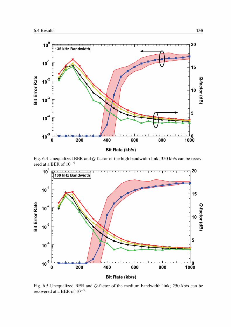
6.4 Results 135
Fig. 6.4 Unequalized BER and Q-factor of the high bandwidth link; 350 kb/s can be recov-ered at a BER of 10−5
Fig. 6.5 Unequalized BER and Q-factor of the medium bandwidth link; 250 kb/s can berecovered at a BER of 10−5
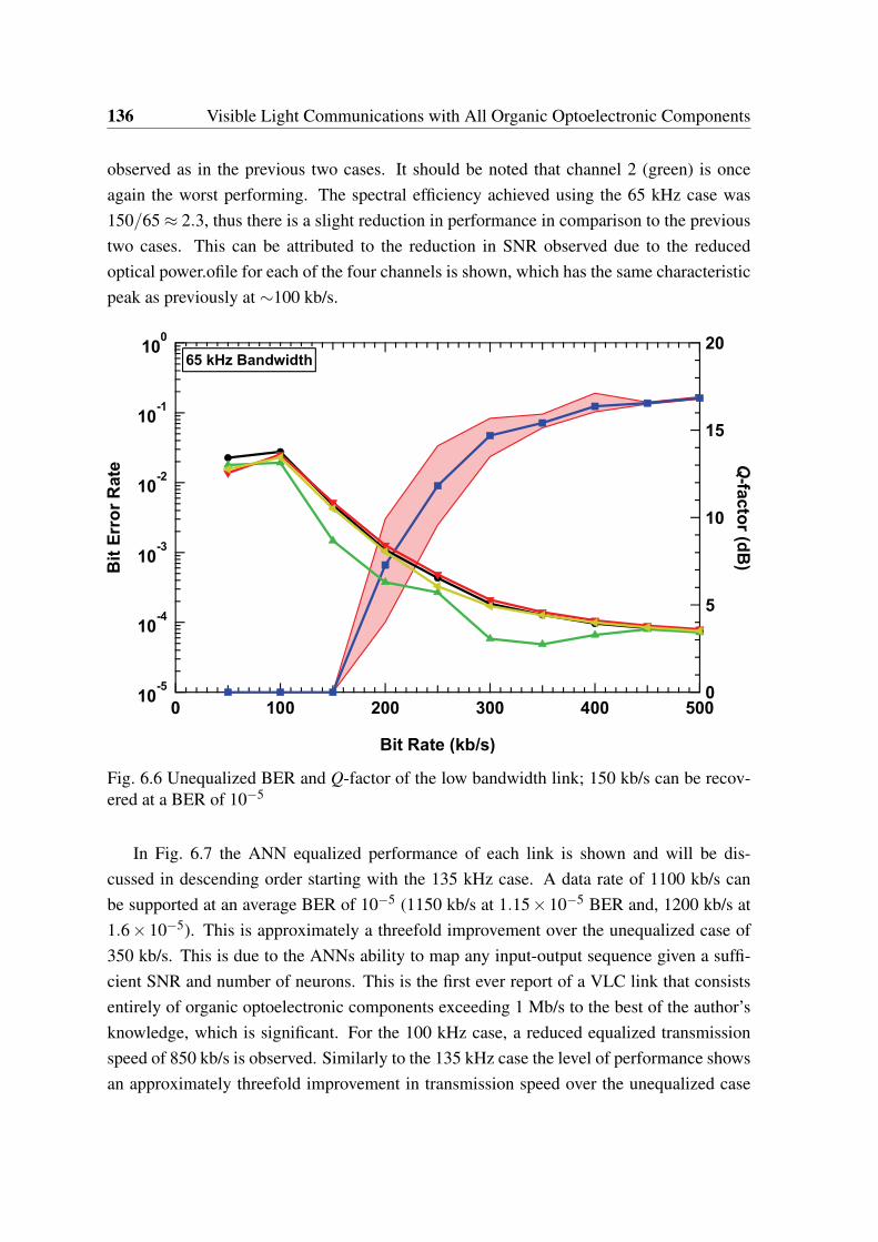
136 Visible Light Communications with All Organic Optoelectronic Components
observed as in the previous two cases. It should be noted that channel 2 (green) is onceagain the worst performing. The spectral efficiency achieved using the 65 kHz case was150/65 ≈ 2.3, thus there is a slight reduction in performance in comparison to the previoustwo cases. This can be attributed to the reduction in SNR observed due to the reducedoptical power.ofile for each of the four channels is shown, which has the same characteristicpeak as previously at ∼100 kb/s.
Fig. 6.6 Unequalized BER and Q-factor of the low bandwidth link; 150 kb/s can be recov-ered at a BER of 10−5
In Fig. 6.7 the ANN equalized performance of each link is shown and will be dis-cussed in descending order starting with the 135 kHz case. A data rate of 1100 kb/s canbe supported at an average BER of 10−5 (1150 kb/s at 1.15×10⁻⁵ BER and, 1200 kb/s at1.6× 10−5). This is approximately a threefold improvement over the unequalized case of350 kb/s. This is due to the ANNs ability to map any input-output sequence given a suffi-cient SNR and number of neurons. This is the first ever report of a VLC link that consistsentirely of organic optoelectronic components exceeding 1 Mb/s to the best of the author’sknowledge, which is significant. For the 100 kHz case, a reduced equalized transmissionspeed of 850 kb/s is observed. Similarly to the 135 kHz case the level of performance showsan approximately threefold improvement in transmission speed over the unequalized case

6.5 Summary 137
(250 kb/s). Finally in the 65 kHz case, an equalized data rate of 450 kb/s can be achieved;once more offering similar performance improvement statistics as the previous two cases.
Fig. 6.7 Equalized BER performance of each of the three cases; data rates of 1100, 850and 450 kb/s can be recovered at a BER of 10−5 for the 135, 100 and 65 kHz bandwidths,respectively
6.5 Summary
In this chapter the first ever OVLC link at a transmission speed exceeding 1 Mb/s has beendemonstrated. The modulation format used was OOK due to its simplicity and compatibilitywith digital equalizers. The equalizer used to achieve such a transmission speed was theANN due to its superiority over other equalizers. As mentioned, organic devices can beproduced with low cost manufacturing methods such as spray coating (as in the OPDs usedhere) which are extremely attractive for implementation in future mobile devices. The final1 Mb/s data rate is a significant result for the field of VLC as organic devices offer significantpromise for applications that are not ideally suited for conventional devices such as mobiledevice communications.


Chapter 7
Visible Light Communications withPolymer Light-Emitting Diodes
7.1 Introduction
PLEDs have been gaining substantial attention in recent years due to their outstanding po-tential for future lighting and display applications [162]. Advantages of PLEDS includelow-cost solvent-based processing, which in turn means large area devices are palpable withrelative ease in comparison to inorganic LEDs.
As with white LEDs, white PLEDs are also seen as a viable source in VLC offeringsimultaneous illumination and data communications within rooms/offices environment. Inboth organic and inorganic VLC there is a common desire to drive up the data rate and thisis reflected in the literature; PLEDs have reached 2.7 Mb/s transmission speeds using OOKand an ‘offline’ multi-layer perceptron ANN based equalizer [163]. On the other hand, in-organic VLC offers data rates up to 3.4 Gb/s [47] using discrete multi-tone modulation andwavelength division multiplexing of red, green and blue wavelengths. Thus it is clear thatthe state-of-the-art transmission speed in OLED-VLC currently lags LED-VLC by aroundthree orders of magnitude. The reason for this disparity is because organic semiconduc-tors are characterized by lower charge mobility than inorganic LEDs by several orders ofmagnitude. Typical hole mobilities of the semiconductors used in PLEDs are in the range10−6-10−2 cm2/Vs, and similar or lower mobilities are found for electrons. Therefore,upon device switch off, extraction of the charge and extinction of the electroluminescenceis therefore slow, despite an exciton lifetime of (typically) less than a nanosecond. Thebandwidth is therefore several orders of magnitude smaller than for inorganic devices. Inthis chapter an increase in the transmission speed is reported for PLED-VLC up to 10 Mb/s;

140 Visible Light Communications with Polymer Light-Emitting Diodes
using a custom designed PLED with a bandwidth of 270 kHz as the transmitter and a PINphotodetector as the receiver is reported. Such a data rate is achieved using a LMS adaptiveequalizer implemented as a finite impulse response (FIR) filter on a Xilinx Virtex 6 ML605FPGA in real time. All the previous literature on increasing data rates in organic VLC usingequalizers has relied on offline processing in MATLAB [163] and hence this is the first timea real time system is reported.
7.2 Production and Characterization of the PLEDs
A schematic of the PLEDs used in this work is illustrated in Fig. 7.1. PLEDs were preparedstarting with a transparent anode comprised of a thin layer (∼120 nm) of ITO deposited viaa sputtering process on a glass substrate. The ITO surface was cleaned in an acetone and iso-propanol sonication bath followed by an oxygen plasma treatment [9, 12]. Immediately afterthe oxygen plasma treatment, a dispersion 2.8% w/w in H2O of the polymer PEDOT:PSS(Sigma-Aldrich) is spin coated (4,500 rpm for 60 s plus 5,000 rpm for 10 s in air) to obtaina highly conductive polymeric film approximately 80 nm thick. The sample was then an-nealed at 140C for 600 s in a nitrogen atmosphere. A solution 2% w/w in p-xylene of thepolymer TFB (American Dye Source) with a molecular weight Mw = 68,000 is then spincoated (2,500 rpm for 60 s under nitrogen atmosphere) on the sample followed by annealing(140C for ∼1 hour) and slow cooling to increase the crystallinity of the TFB layer. Theamorphous portion of TFB is then removed via spin rinsing (1,000 rpm for 30 s and 4,500rpm for 10 s) with p-xylene in which the solvent was added drop-by-drop while spinning.
To deposit the active layer a solution of poly[2-methoxy-5-(3’,7’-dimethyloctyloxy)-1,4-phenylenevinylene] (MDMO-PPV) with a Mn of ∼ 23,000 g/mol (Sigma-Aldrich) 1%w/w in toluene was spin coated (1,800 rpm for 60 s). A metallic calcium cathode 30 nmthick was evaporated onto the active layer and subsequently covered with a 150 nm layerof aluminium as a protection against oxidation. For the evaporation of the cathode a maskto produce eight different pixels was used, see Fig. 7.1. The active area of each pixel is ofabout 3.5 mm2 and it is given by the intersection between the ITO stripe and the calciumlayer. The corresponding energy levels are shown in Fig. 7.2.
The normalized optical emission intensity for each polymer were measured using anAndor spectrometer (Shamrock 163 spectrograph with an Andor Newton EMCCD cam-era) and are shown in Fig. 7.3. The PLEDs have a peak wavelength of 630 nm, with apronounced shoulder at ∼595 nm. The voltage-current density and voltage-optical power(JLV) relationships were measured using a Keithley 2400 voltage source, which suppliedand measured the drive voltage and current. A Keithley 2000 digital multi-meter is used

7.2 Production and Characterization of the PLEDs 141
Calcium
MDMO-PPV
TFB
PEDOT:PSS
ITO
Glass
OCH3
O CH3
CH3CH3
n
N
C8H17 C8H17
n
S
O O
n
SO2H
m
Fig. 7.1 A schematic of the PLED used in this work; the devices are composedof a stack of several thin polymeric layers encapsulated between two planar elec-trodes. The anode is a transparent conductive layer of ITO deposited on a glass sub-strate via a sputtering process. A hole injection layer made of a conjugated poly-mer poly(3,4-ethylenedioxythiophene) and poly(styrenesulfonate) (the mix is referred toas PEDOT:PSS) is in contact with the anode. On top of it, the conjugated polymerpoly[(9’9’-dioctylfluorene-alt-N-(4-butylphenyl)diphenylamine] (TFB) acts as electron-blocking/hole-transporting interlayer [7–9]. The emissive polymer poly[2-methoxy-5-(3’,7’-dimethyloctyloxy)-1,4-phenylenevinylene] (MDMO-PPV) is deposited on top of theTFB and is in direct contact with the metallic calcium cathode which is in turn covered bya layer of aluminium as a protection against oxidation
to measure the voltage from the photodetector, which was converted to the received opticalpower in MATLAB using the responsivity curve of the silicon photodetector. The JLV re-sponse was measured from 0 to 8 V as shown in Fig. 7.4. The operating voltage during thetransmission tests was set at 8 VDC as this value is well above the turn-on for luminescence,therefore offering a milder non-linearity and less distortion to the transmission signal. Al-though at the limit of the range shown in Fig. 7.4, no significant degradation in the deviceoperation was observed during the experiments.
The equalization of the Fermi levels of the electrodes generates a built-in voltage (VBI)across the semiconductor layers inside the device. When the voltage supplied to the device

142 Visible Light Communications with Polymer Light-Emitting Diodes
Fig. 7.2 The energy-level diagram, relative to vacuum, of the isolated materials used in thefabrication of the PLED. HOMO and LUMO stand for ’highest occupied molecular orbital’and ’lowest unoccupied molecular orbital’ respectively. They indicate the two energy levelsof the molecule that are responsible for its semiconductor behavior in the same way asvalence and conduction bands in inorganic semiconductors. The HOMO and LUMO valuesfor TFB and MDMO-PPV are measured by a combination of cyclic voltammetry and opticalabsorption [10, 11]. The Fermi levels of the electrodes are also reported [12]
is above VBI a bipolar injection into the emitting polymer occurs and electroluminescenceensues. The device used in this work shows a peak external quantum efficiency of 1.9%when driving the LED with 72 mA/cm2 current density and an applied voltage of 7.2 Vas shown in Fig. 7.5. Finally, the device bandwidth was measured by transmission of afrequency swept sinusoid (20 kHz - 1 MHz) under the following operating conditions: 8VDC, 4 VAC. At the receiver an Agilent N9010A electrical spectrum analyser measured themagnitude response of the received sinusoid over the given frequency range. Subsequentlythe light was switched off and a noise measurement was made over the same range. Thebandwidth and noise measurements are illustrated in Fig. 7.6 along with the 270 kHz 3-dBpoint for the 270 kHz, which is the bandwidth under the operating conditions listed.
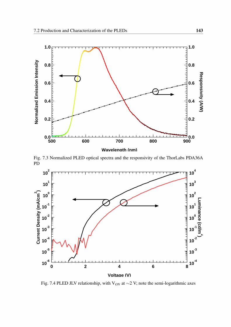
7.2 Production and Characterization of the PLEDs 143
1.0
0.8
0.6
0.4
0.2
0.0
No
rmal
ized
Em
issi
on
Inte
nsi
ty
900800700600500
Wavelength (nm)
1.0
0.8
0.6
0.4
0.2
0.0
Resp
on
sivity (A/W
)
Fig. 7.3 Normalized PLED optical spectra and the responsivity of the ThorLabs PDA36APD
10-6
10-5
10-4
10-3
10-2
10-1
100
101
102
Cu
rren
t D
ensi
ty (
mA
/cm
2 )
86420
Voltage (V)
10-4
10-3
10-2
10-1
100
101
102
103
104
Lu
min
ance (cd
/m2)
Fig. 7.4 PLED JLV relationship, with VON at ∼2 V; note the semi-logarithmic axes
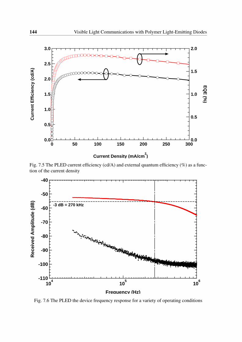
144 Visible Light Communications with Polymer Light-Emitting Diodes
2.0
1.5
1.0
0.5
0.0
EQ
E (%
)
300250200150100500
Current Density (mA/cm2)
3.0
2.5
2.0
1.5
1.0
0.5
0.0
Cu
rren
t E
ffic
ien
cy (
cd/A
)
Fig. 7.5 The PLED current efficiency (cd/A) and external quantum efficiency (%) as a func-tion of the current density
-110
-100
-90
-80
-70
-60
-50
-40
Rec
eive
d A
mp
litu
de
(dB
)
104
105
106
Frequency (Hz)
-3 dB = 270 kHz
Fig. 7.6 The PLED the device frequency response for a variety of operating conditions
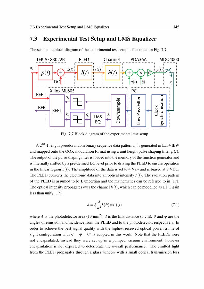
7.3 Experimental Test Setup and LMS Equalizer 145
7.3 Experimental Test Setup and LMS Equalizer
The schematic block diagram of the experimental test setup is illustrated in Fig. 7.7.
p(t) I(t) h(t) ++
×
ℜn(t)DC
x(t) s(t) y(t)ai
yi
qi
ki
BERT
TEK AFG3022B PLED Channel PDA36A MDO4000
Xilinx ML605
BER
LMSEQ D
ow
nsa
mp
le
PC
Clo
ckS
yn
chro
nis
ati
on
Low
Pa
ss F
ilte
rREF di
G
di
Fig. 7.7 Block diagram of the experimental test setup
A 210-1 length pseudorandom binary sequence data pattern ai is generated in LabVIEWand mapped onto the OOK modulation format using a unit height pulse shaping filter p(t).The output of the pulse shaping filter is loaded into the memory of the function generator andis internally shifted by a pre-defined DC level prior to driving the PLED to ensure operationin the linear region x(t). The amplitude of the data is set to 4 VAC and is biased at 8 VDC.The PLED converts the electronic data into an optical intensity I (t). The radiation patternof the PLED is assumed to be Lambertian and the mathematics can be referred to in [17].The optical intensity propagates over the channel h(t), which can be modelled as a DC gainless than unity [17]:
h = ξAd2 I (θ)cos(ϕ) (7.1)
where A is the photodetector area (13 mm2), d is the link distance (5 cm), θ and ϕ are theangles of emission and incidence from the PLED and to the photodetector, respectively. Inorder to achieve the best signal quality with the highest received optical power, a line ofsight configuration with θ = ϕ = 0 is adopted in this work. Note that the PLEDs werenot encapsulated, instead they were set up in a pumped vacuum environment; howeverencapsulation is not expected to deteriorate the overall performance. The emitted lightfrom the PLED propagates through a glass window with a small optical transmission loss

146 Visible Light Communications with Polymer Light-Emitting Diodes
(∼ 10%). Therefore ξ is introduced as a proportionality factor to account for the silicawindow.
No focusing optics were used in the measurements and the distance between PLED anda ThorLabs PDA36A PIN photodetector (with 5.5 MHz bandwidth with an inbuilt tran-simpedance gain of 10 dB) was ∼0.05 m. This is a very short distance in comparison toa full room scale and the reason is because the experiment was performed using singularpixels (∼3.5 mm2) where the brightness was relatively low. To increase the transmissiondistance (>1 m) for future applications, the solution is to simply scale up the amount ofPLEDs until the minimum desired optical power is collected at the receiver. There areseveral sources of noise n(t) including ambient, thermal and shot noise. To minimize theambient noise, the experiment was conducted in a pitch black laboratory. The thermal andshot noise sources are assumed to be AWGN as stated in [17, 111].
The received signal y(t) = Gℜ [h(t)⊗ s(t)+n(t)] is captured and sampled by a Tek-tronix MDO4104-6 real time oscilloscope with the output given by:
yi = Gℜ
yih0 +∞
∑j=−∞
j =i
y jhi− j +ni
(7.2)
where ℜ is the photodiode responsivity, G is the 10 dB transimpedance gain, hi is the sam-pled channel impulse response, i is the current sampling instance, j represents the con-tributions of the ISI and ni is a zero mean Gaussian random variable with variance N0/2representing the noise at each sample. The data yi is acquired by a PC via a LabVIEWscript where synchronization with the transmitted data (clock synchronisation in Fig. 7.7) iscarried out before being passed through a low pass filter (LPF) to remove the high frequencynoise components. Both synchronisation and LPF are not performed in the FPGA domain;this is to ensure that any errors introduced in the system are due to the equalizer in this firstdemonstration of such a link.
To combat ISI, equalizers are the most effective solution; they are typically implementedas digital FIR transversal filters with adjustable coefficients. The adjustment of the equal-izer coefficients is usually carried out adaptively during the transmission process. Duringthe start-up period a short known training sequence is transmitted for the purpose of initialadjustment of the tapped weight coefficients of the filter. The accuracy of the channel esti-mation, which essentially resolves the convergence and performance of equalization, can beaffected either by the length of the training or pilot sequence, or the period between channelestimations. Typically using a higher number of taps will result in better system responseestimation. Likewise, a long training sequence will also result in a better estimation since
7.3 Experimental Test Setup and LMS Equalizer 147
the impact of noise is reduced. On the other hand a high number of taps require more com-putational resources while a long training sequence introduces more redundancy into thesystem due to the requirement for retraining. The tap coefficients are determined using aniterative procedure. The most popular algorithms for determining the tap coefficients arethe LMS, RLS and its derivatives, fast RLS, and gradient RLS. Here the LMS method isemployed in conjunction with the (symbol spaced) linear transversal FIR filter since it is theleast computationally complex of the training algorithms and requires no matrix inversionunlike RLS algorithms. The received samples di are streamed from a PC to the FPGA viaa JTAG Ethernet connection and subsequently down-sampled to one sample-per-bit usinga mid-point sampler before being passed through the filter. Down-sampling, equalization,threshold detection and BERT are all implemented on the FPGA board (Xilinx Virtex 6ML605). The Xilinx ISE software is used to download the synthesized VHDL codes ontothe board. The tap coefficients are updated as follows [161]:
wi+1 (m) = wi (m)+µeidi (7.3)
where di is the incoming noise and interference perturbed downsampled symbol, wi (m) isthe mth filter weight at sample instant i, and µ is the learning rate parameter (set to 0.001) forevery experiment in this work. Setting µ excessively will lead to instability in the equalizer(i.e. never converging) while setting µ insufficiently will result in slow convergence. Thevalue selected for µ is relatively small; however the training length is set to the first 100,000samples thus providing ample time for convergence. Reducing the training sequence lengthwill deteriorate the channel estimation but reduces the SNR penalty and improves the datathroughput.
Once the system response is estimated, the inverse of the system response is applied tothe received symbols by means of tapped weight coefficients in order to recover the originalsymbols. The system is stationary meaning that training only occurs once at the start ofeach measurement. For non-stationary systems it would be expected that a shorter trainingsequence with a larger learning rate parameter would be used due to the need to retrain thetap coefficients when the system response is changing. The output of the equalizer is givenas [161]:
qi =N
∑m=0
wi (m)di−m (7.4)
where N is the number of taps; N = 3; 5; 7; 10; 15; 20; 25. The maximum number oftaps available for this LMS transversal equalizer is 25. The bottleneck is clearly in the IOBs,
148 Visible Light Communications with Polymer Light-Emitting Diodes
which are fully utilized with a 25-tap LMS filter. The rest of the resources are not close tothe capacity (the next most utilized feature is the DSP48s at 27%).
7.4 Results
The BER performance of the system without an equalizer and measured with a symbol-by-symbol threshold detector is shown in Fig. 7.8. Also shown is the Q-factor. It is possibleto transmit up to 3 Mb/s without the use of an equalizer in the real time scenario. Thisis a faster data rate than is currently available in the state-of-the-art organic VLC; which iscurrently limited to 2.7 Mb/s using a highly computationally complex ANN equalizer [163].Aside from the device materials, which can’t be controlled, the key difference betweenthe devices is the bandwidth (∼270 kHz in this work and ∼90 kHz in [163]) due to thephotoactive areas; ∼3.5 mm2 here and ∼4,900 mm2 in [163]. The measured, smoothed andexponentially fitted SNR are shown in Fig. 7.9; the measurement was made by subtractingthe system magnitude response from the system noise floor (refer to Fig. 7.6) between 20kHz - 1 MHz. At 4 MHz the predicted SNR is ∼14 dB, which is sufficient for an OOKlink at a BER of 10−6. Thus it is possible to infer that the link fails as result of higherISI contributions due to the transmission data rate far exceeding the modulation bandwidth.Also shown in inset are the captured eye diagrams.
In order to further improve the available data rate in PLED-VLC systems, it is necssaryto utilise an equalizer as mentioned above. The LMS equalizer with N-taps as previouslydescribed is implemented on the ML605 FPGA board with the BER measurements repeatedfor a range of data rates. The BER performance of the FPGA filter in real time is depictedin Fig. 7.10 showing an improvement with an the increase in the number of taps. For N =
3; 5; 7; 10; 15 taps and at a BER of 10−6 it is possible to increase the data rate by 3 Mb/sto 6 Mb/s compared to the simple threshold detection scheme. For N = 20; 25 taps theavailable error free transmission speed is up to 7 Mb/s at the same BER. This is a significantincrease in the available data rate not only in relation to the threshold detector case (>100%)but also in comparison to the literature [163] with a significantly less complex offline ANNequalizer and also in real time using the FPGA. For data rates >7 Mb/s symbols cannotbe recovered with an acceptable BER. For example, at 8 Mb/s and referring to Fig. 7.9 thepredicted SNR is ∼5 dB and it is for this reason that the equalizer fails because it cannotfilter uncorrelated, and unbounded AWGN.
Thus it is necessary to introduce a BER limit for forward error correction (FEC) at4.6× 10−3, at the cost of 7% increase in the overhead [164], as is a common practice inhigh speed VLCs [47, 58]. The limit is indicated by the dashed line in Fig. 7.10 and it
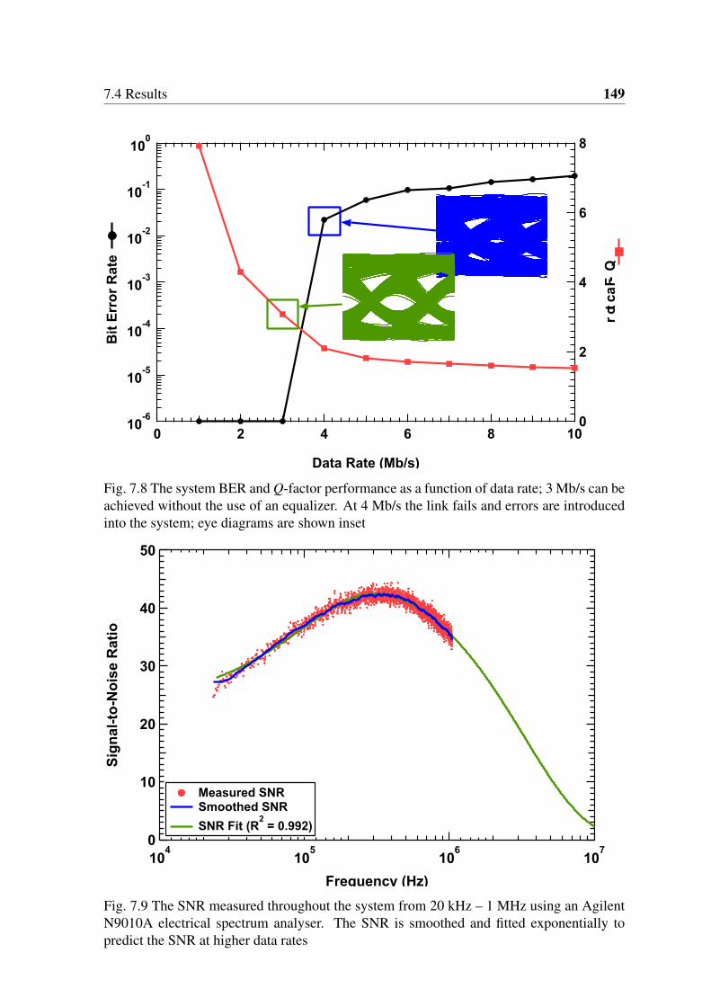
7.4 Results 149
10-6
10-5
10-4
10-3
10-2
10-1
100
Bit
Err
or
Ra
te
1086420
Data Rate (Mb/s)
8
6
4
2
0
Q-F
ac
tor
Fig. 7.8 The system BER and Q-factor performance as a function of data rate; 3 Mb/s can beachieved without the use of an equalizer. At 4 Mb/s the link fails and errors are introducedinto the system; eye diagrams are shown inset
50
40
30
20
10
0
Sig
na
l-to
-No
ise
Ra
tio
104
105
106
107
Frequency (Hz)
Measured SNR Smoothed SNR
SNR Fit (R2 = 0.992)
Fig. 7.9 The SNR measured throughout the system from 20 kHz – 1 MHz using an AgilentN9010A electrical spectrum analyser. The SNR is smoothed and fitted exponentially topredict the SNR at higher data rates

150 Visible Light Communications with Polymer Light-Emitting Diodes
10-6
10-5
10-4
10-3
10-2
Bit
Err
or
Ra
te
1098765
Data Rate (Mb/s)
7% FEC Limit
# Taps: 25 20 15 10 7 5 3
Fig. 7.10 BER performance of the PLED-VLC system with the FPGA based LMS equalizer;clearly there as an increase in performance with an increasing number of taps as expected;the key result is that the 10 Mb/s link has a BER within the FEC limit; meaning that the datacan be recovered with an overhead of just 7%
is clear that data rates can be increased to 10 Mb/s using N = 20 and 25 tapped weightcoefficients. The performance of an equalizer with N = 5; 7; 10; 15 taps show BER of∼0.006 - 0.007 and thus slightly exceeding the FEC limit, while N = 3 taps fails to convergeto the target value. The predicted SNR at a frequency of 10 MHz is <5 dB, where theperformance is descending into the noise floor, which is benefiting from the long traininglength with numerous tapped weight coefficients in order to compose an accurate accountof the channel. Having a FEC overhead of 7% means that the line rate of 10 Mb/s would bereduced to 9.3 Mb/s.
Overall this demonstration of a real time PLED-VLC system operating at an overall datarate of 10 Mb/s is the first real landmark in high speed organic based VLC systems. Thiswork represents three separate increases in the current state-of-the-art data rates over the2.7 Mb/s reported in [163]. Firstly by using a custom produced PLED with ∼3 times largerbandwidth a data rate of 3 Mb/s was possible with simple threshold detection. Secondlyusing the FPGA based LMS equalizer at a BER target of 10−6 a data rate of 7 Mb/s can
7.5 Conclusion 151
be readily achieved. Finally by introducing the FEC BER limit of 4.6× 10⁻³ an overalltransmission speed of 10 Mb/s could be achieved. Removing the 7% redundancy gives anoverall information rate of 9.3 Mb/s, or an increase over [163] by ∼3.5 times whilst using asignificantly less computationally complex equalizer.
7.5 Conclusion
In this work a 10 Mb/s VLC link was implemented using a PLED for the very first time.This transmission speed was achieved at the FEC BER target of 4.6×10⁻³ at the cost of a7% overhead. An LMS equalizer was also adopted and implemented on the Xilinx Virtex 6ML605 FPGA board with 20 and 25 taps. Using 15-tap or fewer does not provide sufficientperformance to achieve such a transmission speed. This is a significant step for the futureof PLED-VLC systems as such a data rate is sufficient for an Ethernet connection.


Chapter 8
Conclusions and Future Work
8.1 Conclusions
The main objective of this thesis was to establish small molecule and polymer OVLC sys-tems into the research community. VLC is an outstanding technology for future the future"last-metre" bottleneck caused by (a) the high capacity ubiquitous backbone networks pro-vided by optical fibre links and (b) considerable overcrowding of the RF spectra. VLCpossesses several serious advantages over RF such as license free use, no electromagneticinterference meaning deployment is possible in sensitive locations such as aircraft and hos-pitals and a wide 400 THz bandwidth (around 10,000 times larger than RF). Thus, VLCis worthy of further research to fulfil its potential. Normally this research has focused onusing inorganic WPLEDs/RGBLEDs as the transmitters and Si PDs as the receivers due toseveral advantages: (i) high optical power output (transmitters) and (ii) reasonable band-widths in the MHz region. On the other hand, such devices also have drawbacks. A few ofthe most noteworthy are scalability due to brittle crystals produced using epitaxial high vac-uum processing methods (transmitters) and low responsivity in the visible range (receivers).Combine these disadvantages with the fact that PLEDs and SMOLEDs are emerging asserious candidates for future lighting systems due to extremely low cost solution-based pro-cessing methods and high electrical efficiencies and the main motivation for this thesis isestablished. Using organic components in general, however, is not an ideal solution. Dueto highly disordered structures with low aggregation charge transport inside the semicon-ductor is roughly three orders of magnitude lower than amorphous Si which causes severelyrestricted bandwidths. Such is the desire of VLC to increase the capacity available to theend-user; the bandwidth limitation is the single most important problem facing OVLC dom-inance. As a result, equalizers are required which permit high transmission speeds by re-moval of ISI either via iterative procedures or by classification. In Chapter 1 this is firmly
154 Conclusions and Future Work
established and aims/objectives are proposed.
In order to fully understand the proposed OVLC field, it was first necessary to estab-lish the fundamental principles of inorganic and organic semiconductor photon generation,emission and absorption which are outlined in Chapter 2. The relationships established inChapter 2 are important because they allow understanding into the behaviour of the deviceswhich is beneficial for later understanding how to establish the best possible transmissionsystem. Simplest-form equivalent circuits are derived from these principles along with gov-erning equations.
Following this, Chapter 3 reviews the theory of optical communications using a math-ematical approach. A full system model is presented including complete analysis of theoptical emission patterns of the transmitters, channel model, reception methods and noisesources. The modulation formats under test in this thesis; OOK and L-PPM are examinedin terms of their probability of error with varying SNR and also their bandwidth, power andspectral efficiency. Finally Chapter 3 covers equalization theory, starting with analogue RCequalization implemented as a passive HPF. It is shown that RC equalization is unsuitablefor low bandwidth applications such as OVLC due to the high power penalty introduced bythe capacitor that causes the BLW phenomenon. As such digital equalizers are introducedthat offer an increase in performance alongside an increase in computational complexity.Digital equalizers can be divided into linear (adaptive and non-adaptive) and non-linear(adaptive) categories and the theory for both is outlined and compared. Finally ANNs areconsidered, in particular the MLP implementation which acts as a universal classifier be-tween input and output sequences. The MLP is established as the best performing equalizerwhilst being the most complex and hence is primarily used in this work.
The objectives of this thesis focus on analysing the performance of several links; aSMOLED to Si PD link and a WPLED to OPD link in the first instance. This allows theestablishment of the BER performance limitations of the individual devices and as such,Chapter 4 marks the beginning of the authors’ original contributions to knowledge. The fullBER analysis of the SMOLED system is outlined. The modulation formats used are OOKand L-PPM. The target BER was set to 10−6 and unequalized (MLP equalized) transmissionspeeds achieved were 50 (2.7), 150 (2.15) and 250 (1.6) kb/s (Mb/s) for 4-PPM, 2-PPM andOOK, respectively. These results were confirmed using a TI TMS320C6713 DSP board thatimplemented the ANN equalizer in real time.
The WPLED/OPD link is analysed in Chapter 5 using OOK and 4-PPM. A further chal-lenge in using OPDs emerges such that the available bandwidth is not constant and dependson the optical power impinging on the active area. The reason for this is due to chargetraps at the interface at energy levels close to those of the HOMO and LUMO. Charge car-
8.1 Conclusions 155
riers propagating through the device may occupy the traps which have an associated timeconstant, which is slower than both the exciton lifetime and the capacitive limit. The timeconstant varies depending on the quantity of filled traps; hence if the impinging light densityis high, the whole population of traps are filled and hence the bandwidth becomes propor-tional to the capacitance which has an upper limit ∼150 - 160 kHz for the devices used inthis thesis. Otherwise the bandwidth is set by the number of traps filled. It should be notedthat the upper bandwidth limitation can be improved by reducing the thickness of the BHJ(∼500 nm in this work); however this is not done here. Therefore Chapter 5 also comparesthe performance of each modulation scheme for a number of incident light densities. Thebandwidths achieved (light densities required) were 160 (300), 110 (270), 76 (50) and 56(10) kHz (µW/cm2). The maximum BER performance of the link with a bandwidth of 160kHz was 500 and 300 kb/s for 4-PPM and OOK, respectively. Using the MLP equalizer and4-PPM, transmission speeds above 1 Mb/s could be achieved in all light densities; (i) 160kHz bandwidth: 3.75 Mb/s transmission speed; (ii) 110 kHz: 2.4 Mb/s; (iii) 76 kHz: 1.45Mb/s and (iv) 56 kHz: 1.15 Mb/s.
The next objective in this thesis was to establish a fully OVLC system that makes useof organic components at each optoelectronic node and this is carried out in Chapter 6. Thelink consisted of the same SMOLED and OPD used in the previous two chapters. The mod-ulation format used was OOK and the unequalized and MLP equalized cases are presentedacross three separate link bandwidths (135, 100 and 65 kHz). The bandwidth is varied bycontrolling the light density of the SMOLED by varying the bias current. The maximumunequalized (equalized) transmission speeds are 350 (1150), 250 (850) and 150 (450) kb/sfor 135, 100 and 65 kHz bandwidths, respectively. This is the first demonstration of a freespace OVLC system and it is remarkable that with such low bandwidths, speeds above 1Mb/s can be supported, which shows a considerable potential for future systems that willoffer improvement on this work.
PLEDs are introduced in Chapter 7 with a view to future solution-processed lightingsolutions that are deployable with extremely low costs. The idea behind the PLEDs used inthis work is to integrate them into active matrices and embed them into display technologiesfor smart homes. Therefore a real time system using an FPGA is proposed and demonstratedwith an LMS linear adaptive equalizer. An error free (10−6) transmission speed of 9.3 Mb/scould be recovered, considering a 7 % FEC code. The gross transmission speed was 10Mb/s which is approaching Ethernet speeds for the first time. Subsequently a remarkableimprovement up to 20 Mb/s could be achieved using the better performing and more com-plex MLP equalizer. A transmission speed of 20 Mb/s is of the upmost importance to theVLC research community because it demonstrates that Ethernet-speed connectivity can be

156 Conclusions and Future Work
achieved using extremely cheap devices which is truly an exciting prospect.
8.2 Future Work
As the author has introduced an entirely new domain for research, it was never intended thatthis work would finish with a complete standalone product. As such there is a huge scopefor future work. The main suggestions of the author are as follows:
8.2.1 Discrete Multi-tone Modulation
DMT has shown remarkable improvements in throughput in the inorganic VLC domain,where transmission speeds at ∼3.4 Gb/s region have been experimentally demonstratedover RGB using links that have bandwidths ∼30 MHz/channel. Therefore DMT is worthyof further investigation for OVLC systems and is not covered at all in this thesis. A detailedinvestigation of the various DMT implementations (asymmetrical, DC-offset, flip) wouldbe advantageous, followed by analysis of the adaptive bit- and power-loading algorithms inorder to further drive up transmission speeds.
8.2.2 Pixel Combining for SNR Improvement
In Chapter 7 PLEDs are introduced for the first time. Despite there being six individualpixels on each substrate only a solitary pixel is used for communications at any given time.The reason for this was due to a shared ITO electrode that means the pixels are not indepen-dent. A lack of independence means a MIMO system is impossible to produce and henceno further measurements were made. The author recommends that a detailed investigationis necessary in order to establish the bandwidth/SNR trade-off that occurs with a varyingnumber of active pixels. If the entire device can simultaneously provide six active pixelsat a minimal bandwidth cost, it is expected that a substantial improvement could be madeon the 20 Mb/s transmission speed reported in Chapter 7 which would be of considerableinterest to the research community.
8.2.3 Reduction of Pixel Size
Considering that the PLEDs used have active area of 3 mm2 they are in an intermediatestate where they are, realistically, too large for smart displays and too small for full roomillumination. A reduction in pixel size would demonstrate an intention to move towardssmart display technologies and would also result in greatly increased bandwidths, estimated

8.2 Future Work 157
to be in the MHz region, thus rivalling WPLEDs. If such devices could be produced, in-dependent of each other on the same substrate then this would be an extremely importantdevelopment for future OVLC systems. Massively MIMO systems could be implementedto offer device-to-device communications in the context of smart homes. Furthermore, theprevious two suggestions can be replicated using the new high-speed independent deviceswith a Gb/s transmission speed target.


References
[1] ThorLabs.
[2] S. Haykin, Adaptive Filter Theory. New Jersey, USA: Prentice Hall International,2001.
[3] “American society for testing and materials (astm) terrestrial reference spectra forphotovoltaic performance evaluation.”
[4] W. Popoola, Subcarrier intensity modulated free-space optical communication sys-tems. Thesis, 2009.
[5] S. Tedde, Design, Fabrication and Characterization of Organic Photodiodes for In-dustrial and Medical Applications. Walter Schottky Institut, Technische UniversitatMunchen, 2009.
[6] A. K. Jain, M. Jianchang, and K. M. Mohiuddin, “Artificial neural networks: a tuto-rial,” Computer, vol. 29, no. 3, pp. 31–44, 1996. 0018-9162.
[7] G. M. Lazzerini, F. Di Stasio, C. Flechon, D. J. Caruana, and F. Cacialli,“Low-temperature treatment of semiconducting interlayers for high-efficiency light-emitting diodes based on a green-emitting polyfluorene derivative,” Applied PhysicsLetters, vol. 99, no. 24, pp. –, 2011.
[8] J.-S. Kim, R. H. Friend, I. Grizzi, and J. H. Burroughes, “Spin-cast thin semicon-ducting polymer interlayer for improving device efficiency of polymer light-emittingdiodes,” Applied Physics Letters, vol. 87, no. 2, pp. –, 2005.
[9] N. Johansson, F. Cacialli, K. Z. Xing, G. Beamson, D. T. Clark, R. H. Friend, andW. R. Salaneck, “A study of the ITO-on-PPV interface using photoelectron spec-troscopy,” Synthetic Metals, vol. 92, no. 3, pp. 207–211, 1998.
[10] O. Fenwick, S. Fusco, T. N. Baig, F. Di Stasio, T. T. Steckler, P. Henriksson, C. Flé-chon, M. R. Andersson, and F. Cacialli, “Efficient red electroluminescence from dike-topyrrolopyrrole copolymerised with a polyfluorene,” APL Materials, vol. 1, no. 3,pp. –, 2013.
[11] B. W. D’Andrade, S. Datta, S. R. Forrest, P. Djurovich, E. Polikarpov, and M. E.Thompson, “Relationship between the ionization and oxidation potentials of molec-ular organic semiconductors,” Organic Electronics, vol. 6, no. 1, pp. 11–20, 2005.

160 References
[12] T. M. Brown and F. Cacialli, “Contact optimization in polymer light-emitting diodes,”Journal of Polymer Science Part B: Polymer Physics, vol. 41, no. 21, pp. 2649–2664,2003.
[13] D. Mange and M. Tomassini, Bio-inspired computing machines: towards novel com-putational architectures. PPUR presses polytechniques, 1998.
[14] R. M. R. Ltd, “Uk radio frequency allocations chart,” 2013.
[15] Y. Ito, “A new paradigm in optical communications and networks,” IEEE Communi-cations Magazine, vol. 51, no. 3, pp. 24–26, 2013.
[16] L. Hanzo, H. Haas, S. Imre, D. O’Brien, M. Rupp, and L. Gyongyosi, “Wirelessmyths, realities, and futures: From 3g/4g to optical and quantum wireless,” Proceed-ings of the IEEE, vol. 100, no. Special Centennial Issue, pp. 1853–1888, 2012.
[17] J. Kahn and J. Barry, “Wireless infrared communications,” Proceedings of the IEEE,vol. 85, no. 2, pp. 265–298, 1997.
[18] J. R. Barry, Wireless Infrared Communications. Boston: Kluwer Academic Publish-ers, 1994.
[19] F. K. Yam and Z. Hassan, “Innovative advances in led technology,” MicroelectronicsJournal, vol. 36, no. 2, pp. 129–137, 2005.
[20] R. D. Dupuis and M. R. Krames, “History, development, and applications of high-brightness visible light-emitting diodes,” Lightwave Technology, Journal of, vol. 26,no. 9, pp. 1154–1171, 2008.
[21] A. Laubsch, M. Sabathil, J. Baur, M. Peter, and B. Hahn, “High-power and high-efficiency ingan-based light emitters,” Electron Devices, IEEE Transactions on,vol. 57, no. 1, pp. 79–87, 2010.
[22] Y. Tanaka, S. Haruyama, and M. Nakagawa, “Wireless optical transmissions withwhite colored led for wireless home links,” in Personal, Indoor and Mobile RadioCommunications, 2000. PIMRC 2000. The 11th IEEE International Symposium on,vol. 2, pp. 1325–1329 vol.2.
[23] Y. Tanaka, T. Komine, S. Haruyama, and M. Nakagawa, “Indoor visible communi-cation utilizing plural white leds as lighting,” in Personal, Indoor and Mobile RadioCommunications, 2001 12th IEEE International Symposium on, vol. 2, pp. F–81–F–85 vol.2.
[24] Y. Tanaka, T. Komine, S. Haruyama, and M. Nakagawa, “A basic study of opticalofdm system for indoor visible communication utilizing plural white leds as lighting,”Proceeding of 8th International Symposium on Microwave and Optical Technology(ISMOT), pp. 303–306, 2001.
[25] K. Fan, T. Komine, Y. Tanaka, and M. Nakagawa, “The effect of reflection on indoorvisible-light communication system utilizing white leds,” in Wireless Personal Multi-media Communications, 2002. The 5th International Symposium on, vol. 2, pp. 611–615 vol.2.
References 161
[26] T. Komine and M. Nakagawa, “Fundamental analysis for visible-light communica-tion system using led lights,” Consumer Electronics, IEEE Transactions on, vol. 50,no. 1, pp. 100–107, 2004.
[27] IEEE, “IEEE standard for local and metropolitan area networks–part 15.7: Short-range wireless optical communication using visible light,” 2012.
[28] K. Lee and H. Park, “Modulations for visible light communications with dimmingcontrol,” IEEE Photonics Technology Letters, vol. 23, no. 16, pp. 1136–1138, 2011.
[29] B. Bo, X. Zhengyuan, and F. Yangyu, “Joint led dimming and high capacity visiblelight communication by overlapping ppm,” in Wireless and Optical CommunicationsConference (WOCC), 2010 19th Annual, pp. 1–5.
[30] K. Jae Kyun, “Inverse source coding for dimming in visible light communicationsusing nrz-ook on reliable links,” IEEE Photonics Technology Letters, vol. 22, no. 19,pp. 1455–1457, 2010.
[31] G. Ntogari, T. Kamalakis, J. Walewski, and T. Sphicopoulos, “Combining illumina-tion dimming based on pulse-width modulation with visible-light communicationsbased on discrete multitone,” IEEE/OSA Journal of Optical Communications andNetworking, vol. 3, no. 1, pp. 56–65, 2011.
[32] C. Joon-ho, C. Eun-byeol, K. Tae-Gyu, and L. Chung Ghiu, “Pulse width modula-tion based signal format for visible light communications,” in OptoeElectronics andCommunications Conference (OECC), 2010 15th, pp. 276–277.
[33] J. Hyung-Joon, C. Joon-Ho, Z. Ghassemlooy, and L. Chung Ghiu, “PWM-based PPMformat for dimming control in visible light communication system,” in Communica-tion Systems, Networks & Digital Signal Processing (CSNDSP), 2012 8th Interna-tional Symposium on, pp. 1–5.
[34] A. Mirvakili and V. J. Koomson, “High efficiency LED driver design for concurrentdata transmission and pwm dimming control for indoor visible light communication,”in Photonics Society Summer Topical Meeting Series, 2012 IEEE, pp. 132–133.
[35] C. Eunbyeol, C. Joon-Ho, P. Chulsoo, K. Moonsoo, S. Seokjoo, Z. Ghassemlooy, andL. Chung Ghiu, “NRZ-OOK signaling with LED dimming for visible light communi-cation link,” in Networks and Optical Communications (NOC), 2011 16th EuropeanConference on, pp. 32–35.
[36] T. Borogovac, M. B. Rahaim, M. Tuganbayeva, and T. D. C. Little, “"lights-off"; vis-ible light communications,” in GLOBECOM Workshops (GC Wkshps), 2011 IEEE,pp. 797–801.
[37] H. Le Minh, D. O’Brien, G. Faulkner, L. Zeng, K. Lee, D. Jung, and Y. Oh, “80 mbit/svisible light communications using pre-equalized white LED,” in Optical Communi-cation, 2008. ECOC 2008. 34th European Conference on, pp. 1–2, IEEE.
[38] H. Le Minh, D. O’Brien, G. Faulkner, L. Zeng, K. Lee, D. Jung, and Y. Oh, “High-speed visible light communications using multiple-resonant equalization,” PhotonicsTechnology Letters, IEEE, vol. 20, no. 14, pp. 1243–1245, 2008.
162 References
[39] H. Le Minh, D. O’Brien, G. Faulkner, L. Zeng, K. Lee, D. Jung, Y. Oh, and E. Won,“100-mb/s NRZ visible light communications using a postequalized white LED,”Photonics Technology Letters, IEEE, vol. 21, no. 15, pp. 1063–1065, 2009.
[40] Z. Ghassemlooy, “Investigation of the baseline wander effect on indoor optical wire-less system employing digital pulse interval modulation,” IET Communications,vol. 2, no. 1, pp. 53–60, 2008. 1751-8628.
[41] A. M. Street, K. Samaras, D. C. Obrien, and D. J. Edwards, “Closed form expressionsfor baseline wander effects in wireless IR applications,” Electronics Letters, vol. 33,no. 12, pp. 1060–1062, 1997.
[42] A. R. Hayes, Z. Ghassemlooy, N. L. Seed, and R. McLaughlin, “Baseline-wandereffects on systems employing digital pulse-interval modulation,” IEE Proceedings -Optoelectronics, vol. 147, no. 4, pp. 295–300, 2000.
[43] J. R. Barry, E. A. Lee, and D. Messerschmitt, Digital Communication. Boston:Kluwer Academic Publishers, 3rd ed., 2003.
[44] J. G. Proakis and M. Salehi, Fundamentals of communication systems. Pearson Pren-tice Hall, 2005.
[45] A. M. Khalid, G. Cossu, R. Corsini, P. Choudhury, and E. Ciaramella, “1-Gb/s trans-mission over a phosphorescent white LED by using rate-adaptive discrete multitonemodulation,” IEEE Photonics Journal, vol. 4, no. 5, pp. 1465–1473, 2012.
[46] R. A. Shafik, S. Rahman, and R. Islam, “On the extended relationships among EVM,BER and SNR as performance metrics,” in Electrical and Computer Engineering,2006. ICECE ’06. International Conference on, pp. 408–411.
[47] G. Cossu, A. M. Khalid, P. Choudhury, R. Corsini, and E. Ciaramella, “3.4 Gbit/s vis-ible optical wireless transmission based on RGB LED,” Opt Express, vol. 20, no. 26,pp. B501–6, 2012.
[48] E. Biglieri, J. Proakis, and S. Shamai, “Fading channels: information-theoretic andcommunications aspects,” IEEE Transactions on Information Theory, vol. 44, no. 6,pp. 2619–2692, 1998.
[49] H. Li, X. Chen, B. Huang, D. Tang, and H. Chen, “High bandwidth visible lightcommunications based on a post-equalization circuit,” Photonics Technology Letters,IEEE, vol. 26, no. 2, pp. 119–122, 2014.
[50] P. A. Haigh, Z. Ghassemlooy, S. Rajbhandari, I. Papakonstantinou, and W. Popoola,“Visible light communications: 170 mb/s using an artificial neural network equalizerin a low bandwidth white light configuration,” Journal of Lightwave Technology,vol. 32, no. 9, pp. 1807–1813, 2014.
[51] J. H. Burroughes, D. D. C. Bradley, A. R. Brown, R. N. Marks, K. Mackay, R. H.Friend, P. L. Burns, and A. B. Holmes, “Light-emitting diodes based on conjugatedpolymers,” Nature, vol. 347, no. 6293, pp. 539–541, 1990. 10.1038/347539a0.
References 163
[52] C. W. Tang and S. A. VanSlyke, “Organic electroluminescent diodes,” AppliedPhysics Letters, vol. 51, no. 12, pp. 913–915, 1987.
[53] C. D. Muller, A. Falcou, N. Reckefuss, M. Rojahn, V. Wiederhirn, P. Rudati,H. Frohne, O. Nuyken, H. Becker, and K. Meerholz, “Multi-colour organic light-emitting displays by solution processing,” Nature, vol. 421, no. 6925, pp. 829–833,2003. 10.1038/nature01390.
[54] S. F. Tedde, J. Kern, T. Sterzl, J. Furst, P. Lugli, and O. Hayden, “Fully spray coatedorganic photodiodes,” Nano Lett, vol. 9, no. 3, pp. 980–3, 2009.
[55] J. Shinar, Organic Light-Emitting Devices: A Survey. Springer, 2003.
[56] Y. Zhao, L. Duan, D. Zhang, L. Hou, J. Qiao, L. Wang, and Y. Qiu, “Small molec-ular phosphorescent organic light-emitting diodes using a spin-coated hole blockinglayer,” Applied Physics Letters, vol. 100, no. 8, p. 083304, 2012.
[57] F. Villani, P. Vacca, G. Nenna, O. Valentino, G. Burrasca, T. Fasolino, C. Minarini,and D. della Sala, “Inkjet printed polymer layer on flexible substrate for oled appli-cations,” The Journal of Physical Chemistry C, vol. 113, no. 30, pp. 13398–13402,2009.
[58] J. Vucic, C. Kottke, S. Nerreter, K. Habel, A. Buttner, K. D. Langer, and J. W.Walewski, “230 Mbit/s via a wireless visible-light link based on OOK modulationof phosphorescent white LEDs,” in Optical Fiber Communication (OFC), collocatedNational Fiber Optic Engineers Conference, 2010 Conference on (OFC/NFOEC),pp. 1–3.
[59] P. A. Haigh, Z. Ghassemlooy, H. L. Minh, S. Rajbhandari, F. Arca, S. F. Tedde,O. Hayden, and I. Papakonstantinou, “Exploiting equalization techniques for improv-ing data rates in organic optoelectronic devices for visible light communications,”Journal of Lightwave Technology, vol. 30, no. 19, pp. 3081–3088, 2012.
[60] R. Das and P. Harrop, “Organic and printed electronics - forecasts, players and op-portunites 2007-2027,” report, IDTechEx, 2010.
[61] F. Arca, S. F. Tedde, M. Sramek, J. Rauh, P. Lugli, and O. Hayden, “Interface trapstates in organic photodiodes,” Sci Rep, vol. 3, p. 1324, 2013.
[62] R. Noriega, J. Rivnay, K. Vandewal, F. P. V. Koch, N. Stingelin, P. Smith, M. F.Toney, and A. Salleo, “A general relationship between disorder, aggregation andcharge transport in conjugated polymers,” Nat Mater, vol. 12, no. 11, pp. 1038–1044,2013.
[63] P. A. Haigh, Z. Ghassemlooy, and I. Papakonstantinou, “1.4-Mb/s white organic LEDtransmission system using discrete multitone modulation,” IEEE Photonics Technol-ogy Letters, vol. 25, no. 6, pp. 615–618, 2013.
[64] N. P. Vlannes and T. M. Lu, “Organic photonics: materials and devices strategy forcomputational and communication systems,” in Telesystems Conference, 1992. NTC-92., National, pp. 9/7–915.
164 References
[65] J. Clark and G. Lanzani, “Organic photonics for communications,” Nat Photon,vol. 4, no. 7, pp. 438–446, 2010. 10.1038/nphoton.2010.160.
[66] S. Valouch, M. Nintz, S. W. Kettlitz, N. S. Christ, and U. Lemmer, “Thickness-dependent transient photocurrent response of organic photodiodes,” IEEE PhotonicsTechnology Letters, vol. 24, no. 7, pp. 596–598, 2012.
[67] B. Arredondo, C. de Dios, R. Vergaz, G. del Pozo, and B. Romero, “High-bandwidthorganic photodetector analyzed by impedance spectroscopy,” IEEE Photonics Tech-nology Letters, vol. 24, no. 20, pp. 1868–1871, 2012.
[68] L. Salamandra, G. Susanna, S. Penna, F. Brunetti, and A. Reale, “Time-resolved re-sponse of polymer bulk-heterojunction photodetectors,” IEEE Photonics TechnologyLetters, vol. 23, no. 12, pp. 780–782, 2011.
[69] E. S. Zaus, S. Tedde, J. Furst, D. Henseler, and G. H. Dohler, “Dynamic and steadystate current response to light excitation of multilayered organic photodiodes,” Jour-nal of Applied Physics, vol. 101, no. 4, pp. 044501–044501–7, 2007.
[70] I. A. Barlow, T. Kreouzis, and D. G. Lidzey, “High-speed electroluminescence modu-lation of a conjugated-polymer light emitting diode,” Applied Physics Letters, vol. 94,no. 24, pp. 243301–3, 2009.
[71] H. Sasabe, J.-i. Takamatsu, T. Motoyama, S. Watanabe, G. Wagenblast, N. Langer,O. Molt, E. Fuchs, C. Lennartz, and J. Kido, “High-efficiency blue and white organiclight-emitting devices incorporating a blue iridium carbene complex,” Advanced Ma-terials, vol. 22, no. 44, pp. 5003–5007, 2010.
[72] T. Chiba, Y.-J. Pu, R. Miyazaki, K.-i. Nakayama, H. Sasabe, and J. Kido, “Ultra-high efficiency by multiple emission from stacked organic light-emitting devices,”Organic Electronics, vol. 12, no. 4, pp. 710–715, 2011.
[73] S. Sze and K. Ng, Physics of semiconductor devices. John Wiley & Sons Inc., 3rd ed.,2007.
[74] S. Pimputkar, J. S. Speck, S. P. DenBaars, and S. Nakamura, “Prospects for LEDlighting,” Nat Photon, vol. 3, no. 4, pp. 180–182, 2009. 10.1038/nphoton.2009.32.
[75] F. A. Ponce and D. P. Bour, “Nitride-based semiconductors for blue and green light-emitting devices,” Nature, vol. 386, no. 6623, pp. 351–359, 1997. 10.1038/386351a0.
[76] B. Saleh and M. Teich, Fundamentals of Photonics. John Wiley & Sons, 2007.
[77] E. Schubert, Light-Emitting Diodes. Boston Univ., 2002.
[78] S. Chuang, Physics of Photonic Devices. Wiley, 2012.
[79] U. Ozgur, H. Liu, L. Xing, X. Ni, and H. Morkoc, “Gan-based light-emitting diodes:Efficiency at high injection levels,” Proceedings of the IEEE, vol. 98, no. 7, pp. 1180–1196, 2010.
[80] W. Shockley, “The theory of p-n junctions in semiconductors and p-n junction tran-sistors,” The Bell System Technical Journal, vol. XXVIII, pp. 335–600, 1949.

References 165
[81] F. Trager, Springer Handbook of Lasers and Optics. Springer, 2012.
[82] H. Le Minh, Z. Ghassemlooy, A. Burton, and P. A. Haigh, “Equalization for organiclight emitting diodes in visible light communications,” 2011.
[83] A. Fox, Optical Properties of Solids. Oxford University Press, 2001.
[84] K. Myny, E. van Veenendaal, G. H. Gelinck, J. Genoe, W. Dehaene, and P. Heremans,“An 8-bit, 40-instructions-per-second organic microprocessor on plastic foil,” Solid-State Circuits, IEEE Journal of, vol. 47, no. 1, pp. 284–291, 2012.
[85] G. E. Moore, “Cramming more components onto integrated circuits,” Proceedings ofthe IEEE, vol. 86, no. 1, pp. 82–85, 1998.
[86] J. Clayden, N. Greeves, and S. Warren, Organic Chemistry. OUP Oxford, 2012.
[87] P. Atkins and J. de Paula, Physical Chemistry. W. H. Freeman, 2009.
[88] J. Frenkel, “On the transformation of light into heat in solids. i,” Physical Review,vol. 37, no. 1, pp. 17–44, 1931. PR.
[89] J. Frenkel, “On the transformation of light into heat in solids. ii,” Physical Review,vol. 37, no. 10, pp. 1276–1294, 1931. PR.
[90] G. H. Wannier, “The structure of electronic excitation levels in insulating crystals,”Physical Review, vol. 52, no. 3, pp. 191–197, 1937. PR.
[91] W. Brutting, Physics of Organic Semiconductors. Wiley, 2006.
[92] M. Pope and C. Swenberg, Electronic processes in organic crystals and polymers.Oxford University Press, 1999.
[93] Y. Roichman and N. Tessler, “Generalized einstein relation for disorderedsemiconductors—implications for device performance,” Applied Physics Letters,vol. 80, no. 11, pp. 1948–1950, 2002.
[94] L. G. Kaake, P. F. Barbara, and X. Y. Zhu, “Intrinsic charge trapping in organicand polymeric semiconductors: A physical chemistry perspective,” The Journal ofPhysical Chemistry Letters, vol. 1, no. 3, pp. 628–635, 2010.
[95] A. Miller and E. Abrahams, “Impurity conduction at low concentrations,” PhysicalReview, vol. 120, no. 3, pp. 745–755, 1960. PR.
[96] C. Brabec, N. Sariciftci, and J. Hummelen, “Plastic solar cells,” Adv. Funct. Mater.,vol. 11, no. 15, 2001.
[97] P. A. Haigh, Z. Ghassemlooy, I. Papakonstantinou, F. Arca, S. F. Tedde, O. Hayden,and S. Rajbhandari, “A MIMO-ANN system for increasing data rates in organic vis-ible light communications systems,” in IEEE ICC 2013 - Wireless CommunicationsSymposium (ICC’13 WCS).
[98] F. Eder, H. Klauk, M. Halik, U. Zschieschang, G. Schmid, and C. Dehm, “Organicelectronics on paper,” Applied Physics Letters, vol. 84, no. 14, pp. 2673–2675, 2004.
166 References
[99] T. Someya, “Flexible electronics: Tiny lamps to illuminate the body,” Nat Mater,vol. 9, no. 11, pp. 879–880, 2010. 10.1038/nmat2886.
[100] Z. B. Wang, M. G. Helander, J. Qiu, D. P. Puzzo, M. T. Greiner, Z. M. Hudson,S. Wang, Z. W. Liu, and Z. H. Lu, “Unlocking the full potential of organic light-emitting diodes on flexible plastic,” Nat Photon, vol. 5, no. 12, pp. 753–757, 2011.
[101] T.-H. Han, Y. Lee, M.-R. Choi, S.-H. Woo, S.-H. Bae, B. H. Hong, J.-H. Ahn, andT.-W. Lee, “Extremely efficient flexible organic light-emitting diodes with modifiedgraphene anode,” Nat Photon, vol. 6, no. 2, pp. 105–110, 2012.
[102] J. Lambert, Photometria sive de mensura et gradibus luminis colorum et umbrae.Vidvae Eberhardi Klett, 1760.
[103] D. C. O’Brien, L. Zeng, H. Le-Minh, G. Faulkner, J. W. Walewski, and S. Randel,“Visible light communications: Challenges and possibilities,” in Personal, Indoorand Mobile Radio Communications, 2008. PIMRC 2008. IEEE 19th InternationalSymposium on, pp. 1–5.
[104] C. L. Mulder, K. Celebi, K. M. Milaninia, and M. A. Baldo, “Saturated and efficientblue phosphorescent organic light emitting devices with lambertian angular emis-sion,” Applied Physics Letters, vol. 90, no. 21, p. 211109, 2007.
[105] S. Rajbhandari, Application of wavelets and artificial neural network for indoor op-tical wireless communication systems. Thesis, 2010.
[106] L. Couch, Digital and Analog Communication Systems. Prentice Hall, 2007.
[107] A. Carlson, P. Crilly, and P. Crilly, Communication Systems. McGraw-Hill HigherEducation, 2009.
[108] J. Proakis, Digital Communications. New York: McGraw-Hill, 2004.
[109] G. L. Turin, “An introduction to matched filters,” Information Theory, IRE Transac-tions on, vol. 6, no. 3, pp. 311–329, 1960.
[110] S. Sheikh Muhammad, T. Javornik, I. Jelovcan, Z. Ghassemlooy, and E. Leitgeb,“Comparison of hard-decision and soft-decision channel coded m-ary ppm perfor-mance over free space optical links,” European Transaction on Telecommunications,pp. 12, DOI: 10.1002/ett.1343, 2008.
[111] Z. Ghassemlooy, W. Popoola, and S. Rajbhandari, Optical Wireless Communications:System and Channel Modelling. CRC PressINC, 2012.
[112] J. Proakis, Wiley encyclopedia of telecommunications. Wiley-Interscience, 2003.
[113] T. Ohtsuki, “Turbo-coded atmospheric optical communication systems,” in Commu-nications, 2002. ICC 2002. IEEE International Conference on, vol. 5, pp. 2938–2942vol.5.
[114] A. J. Phillips, R. A. Cryan, and J. M. Senior, “An optically preamplified intersatel-lite ppm receiver employing maximum likelihood detection,” Photonics TechnologyLetters, IEEE, vol. 8, no. 5, pp. 691–693, 1996.

References 167
[115] S. Rajbhandari, Z. Ghassemlooy, and M. Angelova, “Bit error performance of diffuseindoor optical wireless channel pulse position modulation system employing artifi-cial neural networks for channel equalisation,” IET Optoelectronics, vol. 3, no. 4,pp. 169–179, 2009.
[116] S. Haykin, Communication Systems, 4th Ed. Wiley India Pvt. Limited, 2008.
[117] K. Samaras, A. M. Street, D. O”Brien, and D. J. Edwards, “Error rate evaluation ofwireless infrared links,” in Communications, 1998. ICC 98. Conference Record. 1998IEEE International Conference on, vol. 2, pp. 826–831 vol.2.
[118] W. S. McCulloch and W. Pitts, “A logical calculus of the ideas immanent in nervousactivity,” The Bulletin of Mathematical Biophysics, vol. 5, no. 4, pp. 115–133, 1943.
[119] F. Rosenblatt, “Principles of neurodynamics,” 1962.
[120] J. Anderson, E. Rosenfeld, and A. Pellionisz, Neurocomputing. MIT Press, 1993.
[121] L. J. Cao and F. E. H. Tay, “Support vector machine with adaptive parameters infinancial time series forecasting,” Neural Networks, IEEE Transactions on, vol. 14,no. 6, pp. 1506–1518, 2003.
[122] S. C. B. Lo, S. L. A. Lou, L. Jyh-Shyan, M. T. Freedman, M. V. Chien, and S. K. Mun,“Artificial convolution neural network techniques and applications for lung noduledetection,” Medical Imaging, IEEE Transactions on, vol. 14, no. 4, pp. 711–718,1995.
[123] B. Widrow and R. Winter, “Neural nets for adaptive filtering and adaptive patternrecognition,” Computer, vol. 21, no. 3, pp. 25–39, 1988.
[124] S. Haykin, Neural networks: A comprehensive foundation. New Jersey, USA: Pren-tice Hall, 2nd ed., 1998.
[125] K. Hornik, M. Stinchcombe, and H. White, “Multilayer feedforward networks areuniversal approximators,” Neural Networks, vol. 2, no. 5, pp. 359 – 366, 1989.
[126] S.-I. Amari and A. Cichocki, “Adaptive blind signal processing-neural network ap-proaches,” Proceedings of the IEEE, vol. 86, no. 10, pp. 2026–2048, 1998.
[127] L. Behera, S. Kumar, and A. Patnaik, “On adaptive learning rate that guarantees con-vergence in feedforward networks,” IEEE Transactions on Neural Networks, vol. 17,no. 5, pp. 1116–1125, 2006.
[128] A. Toledo, M. Pinzolas, J. J. Ibarrola, and G. Lera, “Improvement of the neighbor-hood based levenberg-marquardt algorithm by local adaptation of the learning coef-ficient,” IEEE Trans Neural Netw, vol. 16, no. 4, pp. 988–92, 2005.
[129] S. Rajbhandari, J. Faith, Z. Ghassemlooy, and M. Angelova, “Comparative studyof classifiers to mitigate intersymbol interference in diffuse indoor optical wirelesscommunication links,” Optik - International Journal for Light and Electron Optics,no. 0, 2013.

168 References
[130] S. Trenn, “Multilayer perceptrons: Approximation order and necessary number ofhidden units,” Neural Networks, IEEE Transactions on, vol. 19, no. 5, pp. 836–844,2008. 1045-9227.
[131] H. Zhang, W. Choy, and K. Li, “Blue organic LEDs with improved power efficiency,”IEEE Transactions on Electron Devices, vol. 57, no. 1, pp. 125–128, 2010.
[132] H. Sasabe, K. Minamoto, Y.-J. Pu, M. Hirasawa, and J. Kido, “Ultra high-efficiencymulti-photon emission blue phosphorescent OLEDs with external quantum efficiencyexceeding 40%,” Organic Electronics, vol. 13, no. 11, pp. 2615–2619, 2012.
[133] C. Waechter, D. Michaelis, and N. Danz, “Approaches for tailoring organic LEDemission patterns by microoptics arrays,” in Solid-State and Organic Lighting, Opti-cal Society of America.
[134] T. Bocksrocker, J. B. Preinfalk, J. Asche-Tauscher, A. Pargner, C. Eschenbaum,F. Maier-Flaig, and U. Lemme, “White organic light emitting diodes with enhancedinternal and external outcoupling for ultra-efficient light extraction and lambertianemission,” Optics Express, vol. 20, no. 106, pp. A932–A940, 2012.
[135] P. Freitag, A. A. Zakhidov, B. Luessem, A. Zakhidov, and K. Leo, “Lambertian whitetop-emitting organic light emitting device with carbon nanotube cathode,” Journal ofApplied Physics, vol. 112, no. 11, pp. 114505–114505–5, 2012.
[136] H. T. Nicolai, M. Kuik, G. A. Wetzelaer, B. de Boer, C. Campbell, C. Risko, J. L.Bredas, and P. W. Blom, “Unification of trap-limited electron transport in semicon-ducting polymers,” Nat Mater, vol. 11, no. 10, pp. 882–7, 2012.
[137] K. Szczerba, P. Westbergh, E. Agrell, M. Karlsson, P. A. Andrekson, and A. Lars-son, “Comparison of intersymbol interference power penalties for OOK and 4-PAMin short-range optical links,” Journal of Lightwave Technology, vol. 31, no. 22,pp. 3525–3534, 2013.
[138] A. R. Hayes, Digital Pulse Interval Modulation for Indoor Optical Wireless Commu-nication Systems. Phd, 2002.
[139] ThorLabs, “PDA36A Si switchable gain detector,” 2012.
[140] D. Dilaura, K. Houser, R. Mistrick, and G. Steffy, IES Lighting Handbook. Illumi-nating Engineering.
[141] F. D. Waldhauer, “Quantized feedback in an experimental 280-Mb/s digital repeaterfor coaxial transmission,” IEEE Transactions on Communications, vol. 22, no. 1,pp. 1–5, 1974.
[142] K. Burse, R. N. Yadav, and S. C. Shrivastava, “Channel equalization using neuralnetworks: A review,” IEEE Transactions on Systems, Man, and Cybernetics, Part C(Applications and Reviews), vol. 40, no. 3, pp. 352–357, 2010.
[143] S. Rajbhandari, Z. Ghassemlooy, and D. Lee, “Wavelet-artificial neural network re-ceiver for indoor optical wireless communications,” Journal of Lightwave Technol-ogy, vol. 29, no. 17, pp. 2651–2659, 2011.
References 169
[144] C. Soci, I.-W. Hwang, C. Yang, D. Moses, Z. Zhu, D. Waller, R. Gaudiana, C. J.Brabec, and A. J. Heeger, “Charge carrier photogeneration and transport propertiesof a novel low-bandgap conjugated polymer for organic photovoltaics,” pp. 63340D–63340D, 2006. 10.1117/12.680781.
[145] F. Arca, M. Sramek, S. F. Tedde, P. Lugli, and O. Hayden, “Near-infrared organicphotodiodes,” IEEE Journal of Quantum Electronics, vol. 49, no. 12, pp. 1016–1025,2013.
[146] A. H. Azhar, T. Tran, and D. O’Brien, “A gigabit/s indoor wireless transmission usingMIMO-OFDM visible-light communications,” IEEE Photonics Technology Letters,vol. 25, no. 2, pp. 171–174, 2013.
[147] W.-W. Tsai, Y.-C. Chao, E.-C. Chen, H.-W. Zan, H.-F. Meng, and C.-S. Hsu, “In-creasing organic vertical carrier mobility for the application of high speed bilayeredorganic photodetector,” Applied Physics Letters, vol. 95, no. 21, p. 213308, 2009.
[148] K. Dambul, D. O’Brien, and G. Faulkner, “Indoor optical wireless MIMO systemwith an imaging receiver,” IEEE Photonics Technology Letters, vol. 23, no. 2, pp. 97–99, 2011.
[149] A. Azhar, T.-A. Tran, and D. O’Brien, “Demonstration of high-speed data transmis-sion using MIMO-OFDM visible light communications,” IEEE GLOBECOM 2010Workshops (GC Wkshps), pp. 1052 –1056, 2010.
[150] L. Zeng, D. O’Brien, H. Minh, G. Faulkner, K. Lee, D. Jung, Y. Oh, and E. Won,“High data rate multiple input multiple output (MIMO) optical wireless communica-tions using white led lighting,” IEEE Journal on Selected Areas in Communications,vol. 27, no. 9, pp. 1654–1662, 2009.
[151] R. Mesleh, R. Mehmood, H. Elgala, and H. Haas, “Indoor MIMO optical wire-less communication using spatial modulation,” in IEEE International Conference onCommunications (ICC) 2010, pp. 1–5.
[152] T. Fath, M. Di Renzo, and H. Haas, “On the performance of space shift keying foroptical wireless communications,” in IEEE GLOBECOM 2010 Workshops (GC Wk-shps), pp. 990–994.
[153] Y. A. Alqudah and M. Kavehrad, “MIMO characterization of indoor wireless opticallink using a diffuse-transmission configuration,” IEEE Transactions on Communica-tions, vol. 51, no. 9, pp. 1554–1560, 2003.
[154] H. Klauk, Organic Electronics: Materials, Manufacturing, and Applications. Wiley,2006.
[155] K. K. Sarma and A. Mitra, “Ann based rayleigh multipath fading channel estima-tion of a mimo-ofdm system,” in First Asian Himalayas International ConferenceonInternet, 2009. AH-ICI 2009, pp. 1–5.
[156] L. Zhang and X. Zhang, “Mimo channel estimation and equalization using three-layer neural networks with feedback,” Tsinghua Science and Technology, vol. 12,no. 6, pp. 658–662, 2007.
170 References
[157] J. Barry, J. Kahn, W. Krause, E. Lee, and D. Messerschmitt, “Simulation of multipathimpulse response for indoor wireless optical channels,” IEEE Journal on SelectedAreas in Communications, vol. 11, no. 3, pp. 367 – 379, 1993.
[158] Z. Ghassemlooy, P. A. Haigh, F. Arca, S. F. Tedde, O. Hayden, I. Papakonstantinou,and S. Rajbhandari, “Visible light communications: 3.75 mbits/s data rate with a160 khz bandwidth organic photodetector and artificial neural network equalization[invited],” Photon. Res., vol. 1, no. 2, pp. 65–68, 2013.
[159] P. A. Haigh, F. Bausi, Z. Ghassemlooy, I. Papakonstantinou, H. Le Minh, C. Fléchon,and F. Cacialli, “Visible light communications: real time 10 mb/s link with a lowbandwidth polymer light-emitting diode,” Optics Express, vol. 22, no. 3, pp. 2830–2838, 2014.
[160] P. A. Haigh, Z. Ghassemlooy, S. Rajbhandari, and I. Papakonstantinou, “Visible lightcommunications using organic light emitting diodes,” IEEE Communications Maga-zine, vol. 51, no. 8, pp. 148–154, 2013.
[161] S. U. H. Qureshi, “Adaptive equalization,” Proceedings of the IEEE, vol. 73, no. 9,pp. 1349–1387, 1985.
[162] S. Reineke, F. Lindner, G. Schwartz, N. Seidler, K. Walzer, B. Lussem, andK. Leo, “White organic light-emitting diodes with fluorescent tube efficiency,” Na-ture, vol. 459, no. 7244, pp. 234–238, 2009. 10.1038/nature08003.
[163] P. A. Haigh, Z. Ghassemlooy, I. Papakonstantinou, and H. L. Minh, “2.7 mb/s witha 93-khz white organic light emitting diode and real time ANN equalizer,” IEEEPhotonics Technology Letters, vol. 25, no. 17, pp. 1687–1690, 2013.
[164] F. Chang, K. Onohara, and T. Mizuochi, “Forward error correction for 100 G trans-port networks,” IEEE Communications Magazine, vol. 48, no. 3, pp. S48–S55, 2010.
Related Documents