Germanium profile design options for SiGe LEC HBTs Michael Schroter a, * , Hung Tran a , Wolfgang Kraus b a Department of Electron devices and Integrated Circuits, University of Technology Dresden, Mommsenstr. 13, D-01062 Dresden, Germany b Atmel Germany, Theresienstr. 2, D-7100 Heilbronn, Germany Received 1 June 2003; received in revised form 1 September 2003 The review of this paper was arranged by Prof. S. Cristoloveanu Abstract Silicon–Germanium (SiGe) heterojunction bipolar transistors (HBTs) with a low emitter doping concentration (LEC) are investigated with respect to their electrical characteristics in dependence of the Germanium profile shape. The study is based on one-dimensional (1D) device simulation using a realistic doping and Ge profile as baseline. While keeping the doping profile unchanged the Ge profile is modified to evaluate its impact on major electrical figure of merits such as transit frequency, ideality factor, early voltage, noise figure, as well as on process control monitors (PCMs) such as internal base sheet resistance and area specific depletion capacitances. The variations in electrical characteristics and PCMs are briefly explained on a theoretical basis with regard to the impact on compact and sta- tistical modeling. Ó 2003 Elsevier Ltd. All rights reserved. 1. Introduction SiGe/SiGeC HBTs are becoming available in many high-performance BiCMOS processes thus entering mainstream applications. Presently, two types of vertical device designs are being pursued. The first and by far most popular of those contains a ‘‘conventional’’ base– emitter doping profile with a moderately doped base and a highly-doped emitter as well as a triangular-shaped Ge profile. The latter creates an aiding drift field for the electrons traversing the base, while the bandgap differ- ence at the BE junction is fairly small. The second type is similar to III–V HBTs and contains a fairly high base doping concentration and a low emitter concentration (LEC). Sufficient current gain is realized here by a sig- nificant bandgap difference at the BE junction that is created through a significant step of the Ge contents. Although LEC HBTs are––from their basic con- cept––in many respects electrically advantageous over conventional designs, their performance seems to be lagging behind. Reasons for this are that (i) aggressive vertical profile optimization as well as lateral scaling through advanced CMOS lithography have not been applied yet to LEC HBTs and (ii) just a single foundry so far has made such a process manufacturable [1]. The present process version contains a box-shaped base doping and Ge profile and achieves a peak transit fre- quency f T of about 45 GHz [1]. In this paper, therefore, possible improvements in the vertical device design for the next generation (f T 90 GHz) of LEC HBTs are investigated. An important goal is also to provide a feeling for the sensitivity of the electrical transistor per- formance with respect to the Ge profile shape. This is of high interest both for compact transistor model devel- opment (such as HICUM [8]), which requires to make simplifying assumptions based on the relative impor- tance of various influence factors, and for statistical modeling, which requires knowledge about the impact of Ge profile variations on key electrical characteristics as well as on process control monitors (PCMs). * Corresponding author. Tel.: +49-351-463-37686; fax: +49- 351-463-37260. E-mail address: [email protected] (M. Schroter). 0038-1101/$ - see front matter Ó 2003 Elsevier Ltd. All rights reserved. doi:10.1016/j.sse.2003.12.004 Solid-State Electronics 48 (2004) 1133–1146 www.elsevier.com/locate/sse

Welcome message from author
This document is posted to help you gain knowledge. Please leave a comment to let me know what you think about it! Share it to your friends and learn new things together.
Transcript
Solid-State Electronics 48 (2004) 1133–1146
www.elsevier.com/locate/sse
Germanium profile design options for SiGe LEC HBTs
Michael Schroter a,*, Hung Tran a, Wolfgang Kraus b
a Department of Electron devices and Integrated Circuits, University of Technology Dresden, Mommsenstr. 13,
D-01062 Dresden, Germanyb Atmel Germany, Theresienstr. 2, D-7100 Heilbronn, Germany
Received 1 June 2003; received in revised form 1 September 2003
The review of this paper was arranged by Prof. S. Cristoloveanu
Abstract
Silicon–Germanium (SiGe) heterojunction bipolar transistors (HBTs) with a low emitter doping concentration
(LEC) are investigated with respect to their electrical characteristics in dependence of the Germanium profile shape. The
study is based on one-dimensional (1D) device simulation using a realistic doping and Ge profile as baseline. While
keeping the doping profile unchanged the Ge profile is modified to evaluate its impact on major electrical figure of
merits such as transit frequency, ideality factor, early voltage, noise figure, as well as on process control monitors
(PCMs) such as internal base sheet resistance and area specific depletion capacitances. The variations in electrical
characteristics and PCMs are briefly explained on a theoretical basis with regard to the impact on compact and sta-
tistical modeling.
� 2003 Elsevier Ltd. All rights reserved.
1. Introduction
SiGe/SiGeC HBTs are becoming available in many
high-performance BiCMOS processes thus entering
mainstream applications. Presently, two types of vertical
device designs are being pursued. The first and by far
most popular of those contains a ‘‘conventional’’ base–
emitter doping profile with a moderately doped base and
a highly-doped emitter as well as a triangular-shaped Ge
profile. The latter creates an aiding drift field for the
electrons traversing the base, while the bandgap differ-
ence at the BE junction is fairly small. The second type is
similar to III–V HBTs and contains a fairly high base
doping concentration and a low emitter concentration
(LEC). Sufficient current gain is realized here by a sig-
nificant bandgap difference at the BE junction that is
created through a significant step of the Ge contents.
* Corresponding author. Tel.: +49-351-463-37686; fax: +49-
351-463-37260.
E-mail address: [email protected] (M. Schroter).
0038-1101/$ - see front matter � 2003 Elsevier Ltd. All rights reserv
doi:10.1016/j.sse.2003.12.004
Although LEC HBTs are––from their basic con-
cept––in many respects electrically advantageous over
conventional designs, their performance seems to be
lagging behind. Reasons for this are that (i) aggressive
vertical profile optimization as well as lateral scaling
through advanced CMOS lithography have not been
applied yet to LEC HBTs and (ii) just a single foundry so
far has made such a process manufacturable [1]. The
present process version contains a box-shaped base
doping and Ge profile and achieves a peak transit fre-
quency fT of about 45 GHz [1]. In this paper, therefore,
possible improvements in the vertical device design for
the next generation (fT � 90 GHz) of LEC HBTs are
investigated. An important goal is also to provide a
feeling for the sensitivity of the electrical transistor per-
formance with respect to the Ge profile shape. This is of
high interest both for compact transistor model devel-
opment (such as HICUM [8]), which requires to make
simplifying assumptions based on the relative impor-
tance of various influence factors, and for statistical
modeling, which requires knowledge about the impact of
Ge profile variations on key electrical characteristics as
well as on process control monitors (PCMs).
ed.
1134 M. Schroter et al. / Solid-State Electronics 48 (2004) 1133–1146
So far, device design studies for LEC HBTs have
received relatively little attention. There has been quite a
variety of work dealing with analytical studies regarding
the ‘‘optimum’’ Ge profile shape that minimizes the base
transit time at low current densities, often resulting in
impractical profiles from a manufacturability point of
view. In a more adequate study [2], the transit and
maximum oscillation frequency were investigated for a
triangular and box Ge profile shape. In [3], a device
simulation study for optimizing the Ge profile with re-
spect to minimizing the noise figure was presented, that
was based on a conventional, i.e. not a LEC, doping
profile. So far, the most comprehensive study on the
dependence of a variety of figures of merits (FoMs),
including ideality, early effect and transit frequency, in
LEC HBTs can be found in [4]. The study dealt with the
Ge (box-)profile variation at the BE junction and was
based on a very early version of the process in [1], that
since then has been significantly modified to make it
manufacturable. In general, for application-specific
process optimization there are many aspects of impor-
tance, that include (i) a variety of FoMs such as transit
frequency, ideality, early effect, noise; (ii) the bias
dependence and high-current behavior; and (iii) the
spatial alignment and variation of the Ge profile with
respect to both junctions. Therefore, this paper focuses
on the impact of the Ge profile design on the above
mentioned aspects, including the relevant PCMs. In
addition, explanations for the observed electrical varia-
tions are provided based on theory, which has to be
somewhat limited though due to the lack of space.
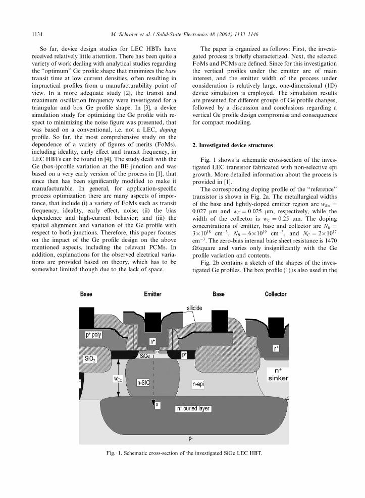
Fig. 1. Schematic cross-section of th
The paper is organized as follows: First, the investi-
gated process is briefly characterized. Next, the selected
FoMs and PCMs are defined. Since for this investigation
the vertical profiles under the emitter are of main
interest, and the emitter width of the process under
consideration is relatively large, one-dimensional (1D)
device simulation is employed. The simulation results
are presented for different groups of Ge profile changes,
followed by a discussion and conclusions regarding a
vertical Ge profile design compromise and consequences
for compact modeling.
2. Investigated device structures
Fig. 1 shows a schematic cross-section of the inves-
tigated LEC transistor fabricated with non-selective epi
growth. More detailed information about the process is
provided in [1].
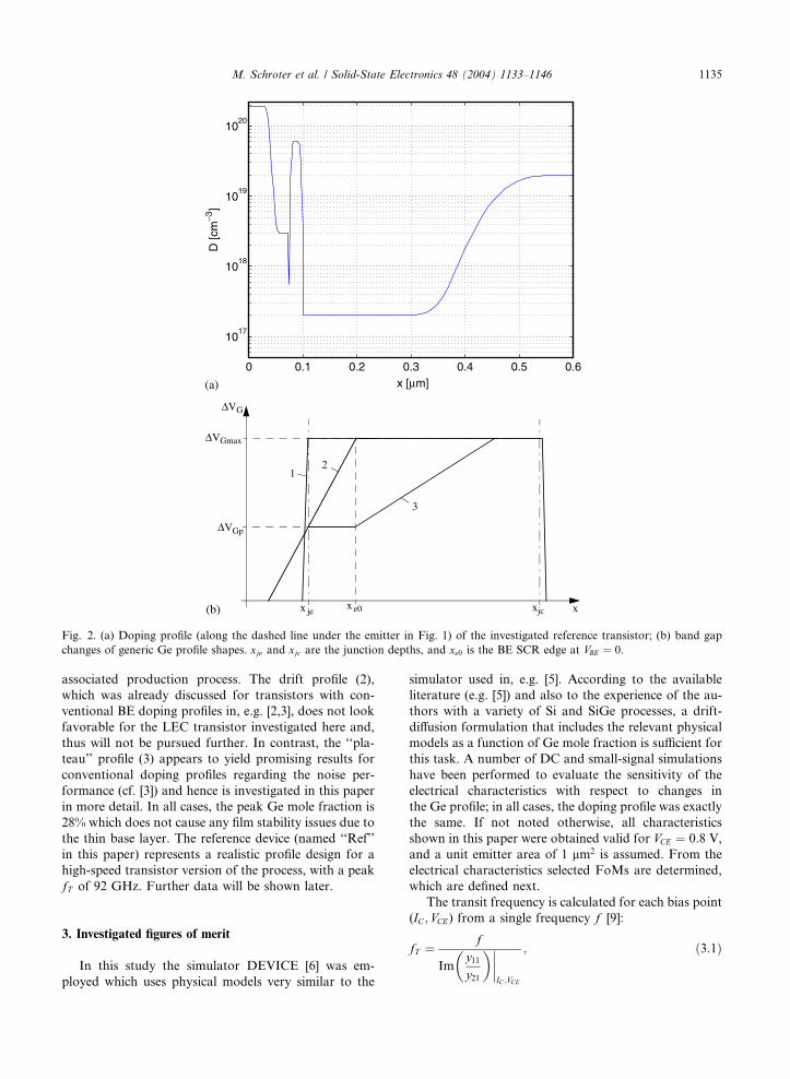
The corresponding doping profile of the ‘‘reference’’
transistor is shown in Fig. 2a. The metallurgical widths
of the base and lightly-doped emitter region are wBm ¼0:027 lm and wE ¼ 0:025 lm, respectively, while the
width of the collector is wC ¼ 0:25 lm. The doping
concentrations of emitter, base and collector are NE ¼3 · 1018 cm�3, NB ¼ 6 · 1019 cm�3, and NC ¼ 2 · 1017cm�3. The zero-bias internal base sheet resistance is 1470
X/square and varies only insignificantly with the Ge
profile variation and contents.
Fig. 2b contains a sketch of the shapes of the inves-
tigated Ge profiles. The box profile (1) is also used in the
e investigated SiGe LEC HBT.
0 0.1 0.2 0.3 0.4 0.5 0.6
1017
1018
1019
1020
D [c
m−3
]
x [µm]
xxjc
∆VG
∆VGmax
x e0
2
3
x je
1
∆VGp
(a)
(b)
Fig. 2. (a) Doping profile (along the dashed line under the emitter in Fig. 1) of the investigated reference transistor; (b) band gap
changes of generic Ge profile shapes. xje and xjc are the junction depths, and xe0 is the BE SCR edge at VBE ¼ 0.
M. Schroter et al. / Solid-State Electronics 48 (2004) 1133–1146 1135
associated production process. The drift profile (2),
which was already discussed for transistors with con-
ventional BE doping profiles in, e.g. [2,3], does not look
favorable for the LEC transistor investigated here and,
thus will not be pursued further. In contrast, the ‘‘pla-
teau’’ profile (3) appears to yield promising results for
conventional doping profiles regarding the noise per-
formance (cf. [3]) and hence is investigated in this paper
in more detail. In all cases, the peak Ge mole fraction is
28% which does not cause any film stability issues due to
the thin base layer. The reference device (named ‘‘Ref’’
in this paper) represents a realistic profile design for a
high-speed transistor version of the process, with a peak
fT of 92 GHz. Further data will be shown later.
3. Investigated figures of merit
In this study the simulator DEVICE [6] was em-
ployed which uses physical models very similar to the
simulator used in, e.g. [5]. According to the available
literature (e.g. [5]) and also to the experience of the au-
thors with a variety of Si and SiGe processes, a drift-
diffusion formulation that includes the relevant physical
models as a function of Ge mole fraction is sufficient for
this task. A number of DC and small-signal simulations
have been performed to evaluate the sensitivity of the
electrical characteristics with respect to changes in
the Ge profile; in all cases, the doping profile was exactly
the same. If not noted otherwise, all characteristics
shown in this paper were obtained valid for VCE ¼ 0:8 V,and a unit emitter area of 1 lm2 is assumed. From the
electrical characteristics selected FoMs are determined,
which are defined next.
The transit frequency is calculated for each bias point
(IC; VCE) from a single frequency f [9]:
fT ¼ f
Imy11y21
� �����IC ;VCE
; ð3:1Þ
1136 M. Schroter et al. / Solid-State Electronics 48 (2004) 1133–1146
with y21 and y11 as transconductance and input admit-
tance in common-emitter configuration, respectively.
Note, that fT can also be calculated as 1=ð2pdQp=dICÞwith Qp as hole charge entering the base. The maximum
value fT ;p has been selected as the first FoM; in addition,
the corresponding current, IC;p, is also determined, since
it provides useful information about the current drive
capability and power consumption (at high speed oper-
ation) of a process. Since fT is a compound variable, the
transit time sf 0 at low current densities is calculated
from fT using the same method as for measurements
(e.g. [11]). This provides more detailed information on
the cause of variations in fT around the peak.
The ideality of the ICðVBEÞ characteristics determines,e.g., the maximum achievable transconductance, and
depends strongly on the Ge profile at the BE junction as
will be explained later. Thus, a useful FoM is the ideality
factor
mCf ¼ ICVT gm
����ðIC0 ;VCE0Þ
; ð3:2Þ
with the low-frequency transconductance gm and the
thermal voltage VT . Since the ideality factor is slightly biasdependent at low current densities, it is calculated at a
given bias point ðIC0; VCE0Þ ¼ ð0:1 mA; 0:8 VÞ. Note thatdue to the exponential transfer characteristics relatively
small changes in mCf can cause large variations in IC .Another important FoM for analog circuit design is
the early voltage VA, defined as
VA ¼ ICgo
����ðIC0 ;VCE0Þ
ð3:3Þ
with go as output conductance. Since VA is bias depen-
dent, it is defined here at the bias point given before.
For RF circuit design, noise plays an important role.
For the purpose of this work, the high-frequency noise
factor was calculated from small-signal simulations
according to [10]
Fmin ¼ 1þ ICVT jy21j2
ffiffiffiffiffiffiffiffiffiffiffiffiffiffiffiffiffiffiffiffiffiffiffiffiffiffiffiffiffiffiffiffiffiffiffiffiffiffiffiffiffiffiffiffiffiffiffiffiffiffiffiffiffiffiffiffiffiffiffiffiffiffiffiffiffiffiffiffiffiffiffiffiffiffiffiffiffiffiffiffiffiffiffiffiffiffiffiffiffiffiffiffiffiffiffiffiffiffiffiffiffiffiffiffiffiffiffiffiffiffiffiffiffiIBIC
jy21j2 þ jy11j2� �
1þ 2VT jy21j2ðrE þ rBÞIC
!� Im2fy11g
vuut0@ þRefy11g
1A ð3:4Þ
which is well suited to observe trends and predicts
absolute values with reasonable accuracy. As FoM, here
the minimum value of the noise figure, NFmin ¼10 logðFminÞ, has been selected that is obtained from a
collector current sweep at f ¼ 2 and 6 GHz. In order to
obtain realistic values, a representative transistor with
an emitter window size of 0.5 · 20 lm2 was assumed
using typical values for the emitter (rE) and external base(rBx) resistance, respectively, while the internal base
resistance rBi was calculated directly from the simulated
sheet resistance under the emitter.
Finally, also the DC current gain,
B ¼ ICIB
����ðIC0 ;VCE0Þ
ð3:5Þ
is considered as FoM. Its absolute value depends on
many effects and the process recipe for, e.g., the emitter
formation. Therefore, 1D simulation cannot be expected
to provide correct absolute values, but can predict
trends and, in particular, the relative impact of bandgap
variations.
In some investigations based on a 1D analysis (e.g.,
[3]), a maximum oscillation frequency fmax is also con-
sidered as FoM. First of all and fundamentally, fmax isnot a clearly defined variable as there are various defi-
nitions, that are more or less useful for circuit design
applications. Second, since in a 1D analysis fmax can
only be calculated based on analytical equations,
assuming a fictitious emitter size, more or less arbitrary
numbers are obtained. Third, using the simple standard
equation for fmax (as in [3]) can result in errors as much
as 100% depending on, e.g., the transistor substrate
network. As a consequence, evaluating fmax for an
investigation of the intrinsic transistor does not provide
any new information.
The PCMs of the intrinsic transistor include the zero-
bias internal base sheet resistance rSBi0, the area specificzero-bias base–emitter depletion capacitance CjE0 and
base–collector depletion capacitance CjC0. Their values
are calculated directly by DEVICE, and their variation
as a function of the Ge profile changes will be discussed
in terms of its physical cause.
4. Results
The results are divided into groups targeting a spe-
cific ‘‘topic’’. Table 1 gives an overview on the major
electrical data and results. In addition to the realistic
doping and Ge profiles shown here, ideal profile shapes
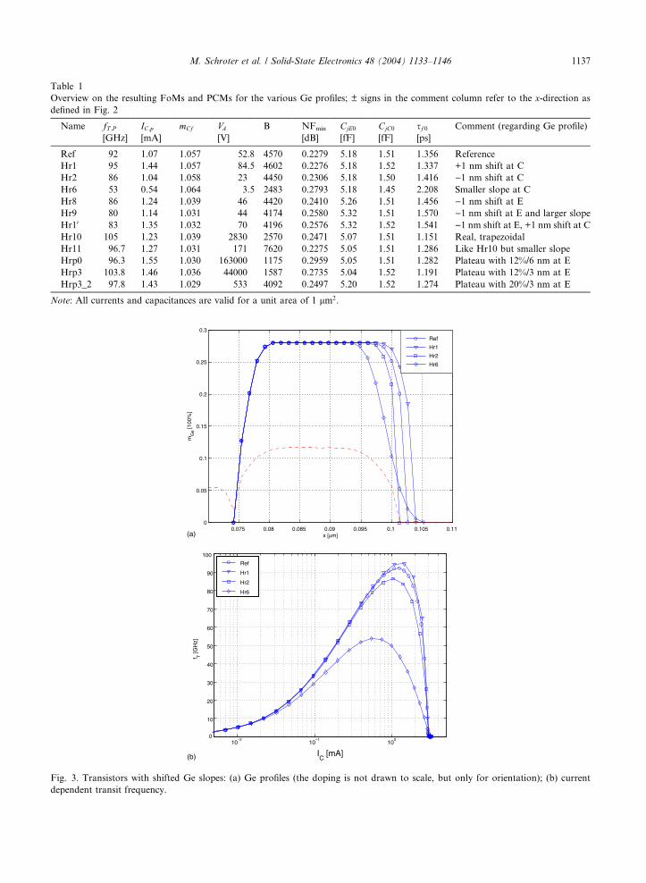
Table 1
Overview on the resulting FoMs and PCMs for the various Ge profiles; ± signs in the comment column refer to the x-direction as
defined in Fig. 2
Name fT ;P[GHz]
IC;p[mA]
mCf VA[V]
B NFmin
[dB]
CjE0
[fF]
CjC0
[fF]
sf 0[ps]
Comment (regarding Ge profile)
Ref 92 1.07 1.057 52.8 4570 0.2279 5.18 1.51 1.356 Reference
Hr1 95 1.44 1.057 84.5 4602 0.2276 5.18 1.52 1.337 +1 nm shift at C
Hr2 86 1.04 1.058 23 4450 0.2306 5.18 1.50 1.416 )1 nm shift at C
Hr6 53 0.54 1.064 3.5 2483 0.2793 5.18 1.45 2.208 Smaller slope at C
Hr8 86 1.24 1.039 46 4420 0.2410 5.26 1.51 1.456 )1 nm shift at E
Hr9 80 1.14 1.031 44 4174 0.2580 5.32 1.51 1.570 )1 nm shift at E and larger slope
Hr10 83 1.35 1.032 70 4196 0.2576 5.32 1.52 1.541 )1 nm shift at E, +1 nm shift at C
Hr10 105 1.23 1.039 2830 2570 0.2471 5.07 1.51 1.151 Real, trapezoidal
Hr11 96.7 1.27 1.031 171 7620 0.2275 5.05 1.51 1.286 Like Hr10 but smaller slope
Hrp0 96.3 1.55 1.030 163000 1175 0.2959 5.05 1.51 1.282 Plateau with 12%/6 nm at E
Hrp3 103.8 1.46 1.036 44000 1587 0.2735 5.04 1.52 1.191 Plateau with 12%/3 nm at E
Hrp3_2 97.8 1.43 1.029 533 4092 0.2497 5.20 1.52 1.274 Plateau with 20%/3 nm at E
Note: All currents and capacitances are valid for a unit area of 1 lm2.
0.075 0.08 0.085 0.09 0.095 0.1 0.105 0.110
0.05
0.1
0.15
0.2
0.25
0.3
mG
e [100
%]
x [µm]
Ref
Hr1
Hr2
Hr6
10–2
10–1
100
0
10
20
30
40
50
60
70
80
90
100
IC [mA]
f T [G
Hz]
Ref
Hr1
Hr2
Hr6
(a)
(b)
Fig. 3. Transistors with shifted Ge slopes: (a) Ge profiles (the doping is not drawn to scale, but only for orientation); (b) current
dependent transit frequency.
M. Schroter et al. / Solid-State Electronics 48 (2004) 1133–1146 1137
1138 M. Schroter et al. / Solid-State Electronics 48 (2004) 1133–1146
were simulated in order to develop and confirm a the-
oretical understanding for both compact and statistical
modeling. Detailed theoretical treatment for LEC tran-
sistors will be published in a later paper.
4.1. Shift of Ge slope at the BC junction
It is well known that the drop of the Ge mole fraction
at the BC junction creates a barrier for holes and, at
high current densities, also for electrons (e.g. [16]).
Depending on the Ge mole fraction and profile, the
electron barrier can cause a very sharp drop in fT ðICÞ,which forces circuit designers to take into account
additional margins, thus limiting the benefit of improved
speed for a process. As a consequence, Ge profiles with
variations at the BC junction are investigated here first;
Fig. 3a shows an enlarged view of the Ge profiles.
Transistors Hr1 and Hr2 differ from transistor Ref only
by a 1 nm variation of the Ge slope at the BC junction; in
Hr6, the Ge starts to decrease already at the end of the
neutral base resulting overall in shallower slope (and
smaller total integrated Ge contents).
Fig. 3b shows the resulting transit frequency curves.
It is obvious that moving the Ge into the collector (Hr1)
increases the speed without much change in peak current
density. On the other hand, moving the Ge slope closer
to the junction (Hr2) or a portion of it even into the base
(Hr6) significantly degrades the speed. In the latter case,
fT drops by almost 50%! As a consequence, for avoidinglarge process variations during production it is manda-
tory that even under worst-case processing conditions
the Ge drop stays entirely in the collector. This can be
achieved at the expense of a larger total contents of the
Ge, with the possible risk of film instability or limiting
0 0. 5 1 1.0
0. 1
0. 2
0. 3
0. 4
0. 5
0. 6
0. 7
0. 8
0. 9
1
IC
[m
g mV
T/I C
[1/V
]
Fig. 4. Forward transconductance gmVT =JCð¼ 1=
the maximum value of Ge. However, due to the fact that
in present and future technology generations the base
width decreases without a significant increase in the
peak Ge mole fraction, film instability issues are ex-
pected to disappear. In fact, it has already become fea-
sible to move the Ge drop fairly far into the collector.
An additional simulation, in which the Ge slope was
moved 50 nm into the collector, showed results very
similar to those of Hr1.
Further electrical data obtained for the above vari-
ations are listed in Table 1. The first two columns
summarize the key results of Fig. 3b. Moving the Ge
slope at the BC junction also causes significant varia-
tions in IC;p, B and VA, while the impact on CjC0 is
moderate (about 4%); NFmin changes only little, except
for Hr6. The change in peak fT is largely reflected in the
low-current transit time sf 0. The ideality factor at low
current densities degrades somewhat for Hr6. From a
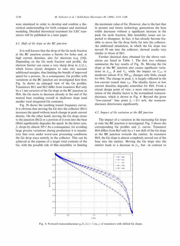
circuit design point of view, a more relevant represen-
tation of the ideality factor is the normalized transcon-
ductance, which is shown in Fig. 4: Beyond the given
‘‘low-current’’ bias point IC ¼ 0:1 mA, the transcon-
ductance deteriorates significantly.
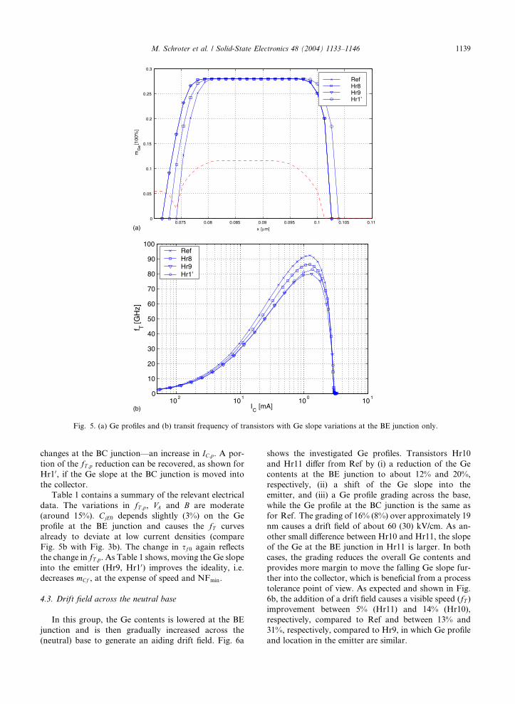
4.2. Impact of Ge variation at the BE junction
The impact of a variation in the increasing Ge slope
at only the BE junction is investigated. Fig. 5 shows the
corresponding Ge profiles and fT curves. Transistor
Hr8 differs from Ref only by a 1 nm shift of the Ge slope
at the BE junction towards the emitter. In transistor
Hr9, the Ge slope is almost completely moved out of the
base into the emitter. Moving the Ge slope into the
emitter leads to a decrease in fT ;p but––in contrast to
5 2 2. 5 3
A]
Ref
Hr1
Hr1´
Hr2
Hr6
mCf Þ of transistors with shifted Ge slopes.
0.075 0.08 0.085 0.09 0.095 0.1 0.105 0.110
0.05
0.1
0.15
0.2
0.25
0.3
mG
e [100
%]
x [µm]
RefHr8Hr9Hr1’
102
101
100
101
0
10
20
30
40
50
60
70
80
90
100
IC
[mA]
f T [GH
z]
RefHr8Hr9Hr1’
(a)
(b)
Fig. 5. (a) Ge profiles and (b) transit frequency of transistors with Ge slope variations at the BE junction only.
M. Schroter et al. / Solid-State Electronics 48 (2004) 1133–1146 1139
changes at the BC junction––an increase in IC;p. A por-
tion of the fT ;p reduction can be recovered, as shown for
Hr10, if the Ge slope at the BC junction is moved into
the collector.
Table 1 contains a summary of the relevant electrical
data. The variations in fT ;p, VA and B are moderate
(around 15%). CjE0 depends slightly (3%) on the Ge
profile at the BE junction and causes the fT curves
already to deviate at low current densities (compare
Fig. 5b with Fig. 3b). The change in sf0 again reflects
the change in fT ;p. As Table 1 shows, moving the Ge slopeinto the emitter (Hr9, Hr10) improves the ideality, i.e.
decreases mCf , at the expense of speed and NFmin.
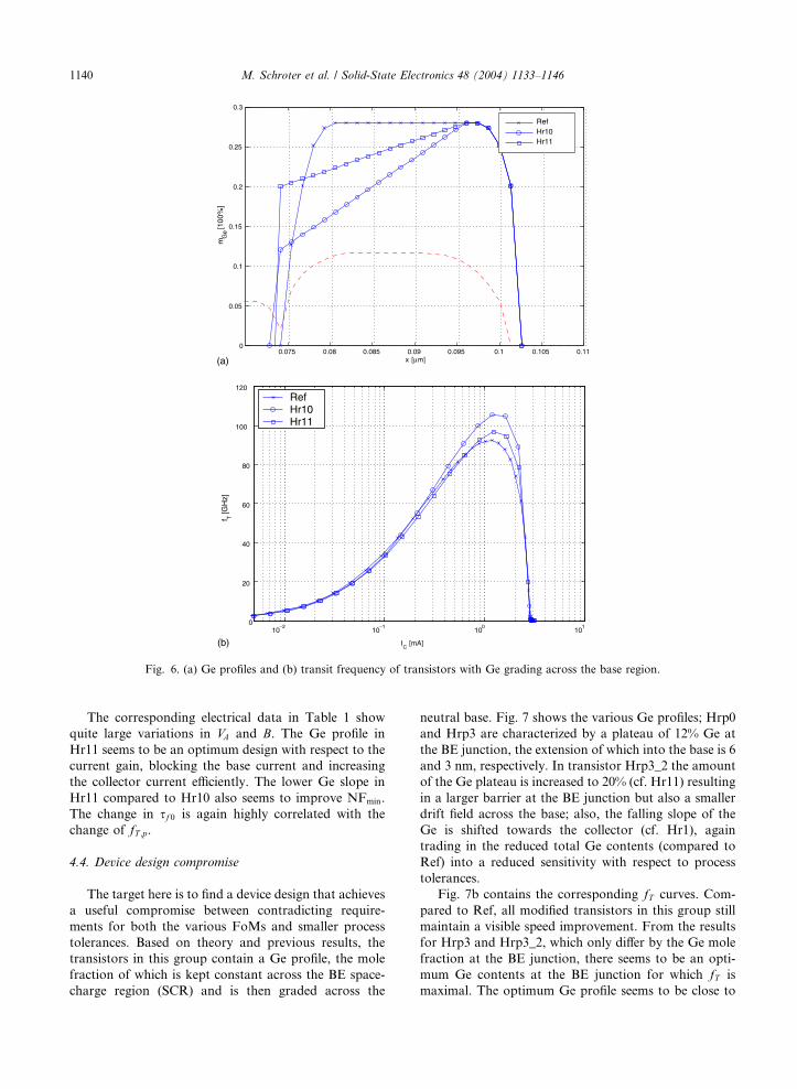
4.3. Drift field across the neutral base
In this group, the Ge contents is lowered at the BE
junction and is then gradually increased across the
(neutral) base to generate an aiding drift field. Fig. 6a
shows the investigated Ge profiles. Transistors Hr10
and Hr11 differ from Ref by (i) a reduction of the Ge
contents at the BE junction to about 12% and 20%,
respectively, (ii) a shift of the Ge slope into the
emitter, and (iii) a Ge profile grading across the base,
while the Ge profile at the BC junction is the same as
for Ref. The grading of 16% (8%) over approximately 19
nm causes a drift field of about 60 (30) kV/cm. As an-
other small difference between Hr10 and Hr11, the slope
of the Ge at the BE junction in Hr11 is larger. In both
cases, the grading reduces the overall Ge contents and
provides more margin to move the falling Ge slope fur-
ther into the collector, which is beneficial from a process
tolerance point of view. As expected and shown in Fig.
6b, the addition of a drift field causes a visible speed (fT )improvement between 5% (Hr11) and 14% (Hr10),
respectively, compared to Ref and between 13% and
31%, respectively, compared to Hr9, in which Ge profile
and location in the emitter are similar.
0.075 0.08 0.085 0.09 0.095 0.1 0.105 0.110
0.05
0.1
0.15
0.2
0.25
0.3
mG
e [100
%]
x [µm]
RefHr10Hr11
10–2
10–1
100
101
0
20
40
60
80
100
120
IC
[mA]
f T [GH
z]
RefHr10Hr11
(a)
(b)
Fig. 6. (a) Ge profiles and (b) transit frequency of transistors with Ge grading across the base region.
1140 M. Schroter et al. / Solid-State Electronics 48 (2004) 1133–1146
The corresponding electrical data in Table 1 show
quite large variations in VA and B. The Ge profile in
Hr11 seems to be an optimum design with respect to the
current gain, blocking the base current and increasing
the collector current efficiently. The lower Ge slope in
Hr11 compared to Hr10 also seems to improve NFmin.
The change in sf 0 is again highly correlated with the
change of fT ;p.
4.4. Device design compromise
The target here is to find a device design that achieves
a useful compromise between contradicting require-
ments for both the various FoMs and smaller process
tolerances. Based on theory and previous results, the
transistors in this group contain a Ge profile, the mole
fraction of which is kept constant across the BE space-
charge region (SCR) and is then graded across the
neutral base. Fig. 7 shows the various Ge profiles; Hrp0
and Hrp3 are characterized by a plateau of 12% Ge at
the BE junction, the extension of which into the base is 6
and 3 nm, respectively. In transistor Hrp3_2 the amount
of the Ge plateau is increased to 20% (cf. Hr11) resulting
in a larger barrier at the BE junction but also a smaller
drift field across the base; also, the falling slope of the
Ge is shifted towards the collector (cf. Hr1), again
trading in the reduced total Ge contents (compared to
Ref) into a reduced sensitivity with respect to process
tolerances.
Fig. 7b contains the corresponding fT curves. Com-
pared to Ref, all modified transistors in this group still
maintain a visible speed improvement. From the results
for Hrp3 and Hrp3_2, which only differ by the Ge mole
fraction at the BE junction, there seems to be an opti-
mum Ge contents at the BE junction for which fT is
maximal. The optimum Ge profile seems to be close to
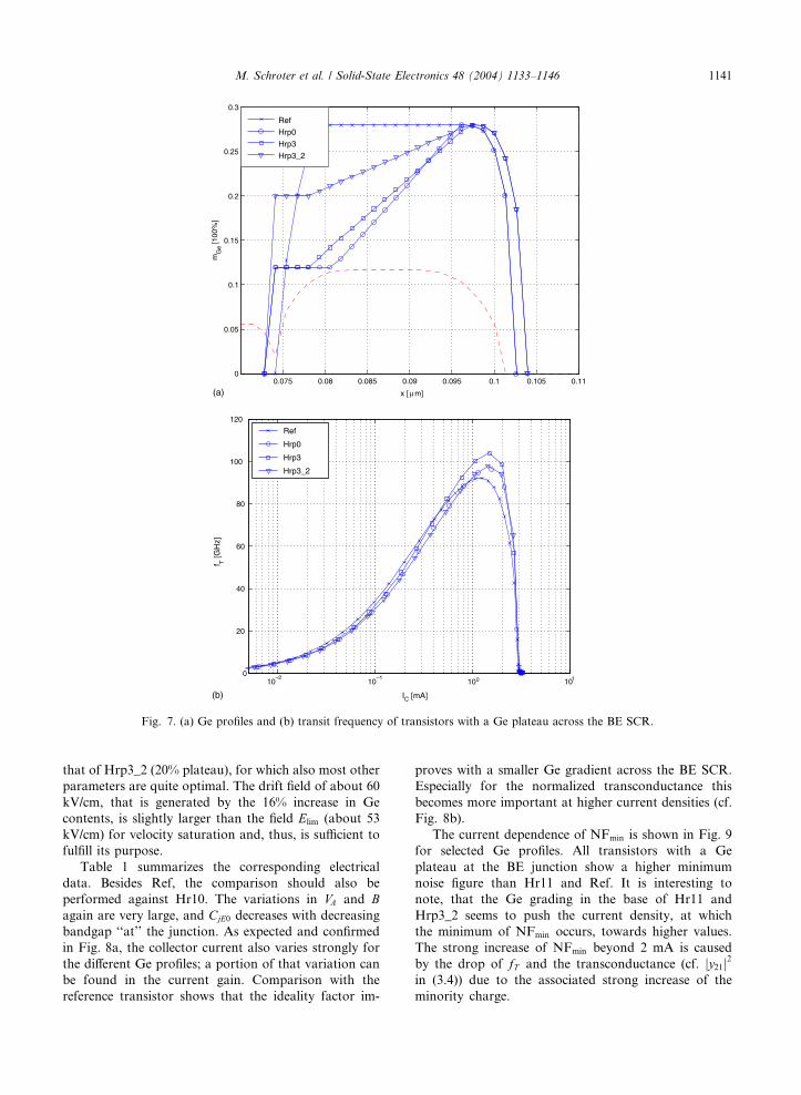
0.075 0.08 0.085 0.09 0.095 0.1 0.105 0.110
0.05
0.1
0.15
0.2
0.25
0.3
mG
e [100
%]
x [µm]
Ref
Hrp0
Hrp3
Hrp3_2
10–2
10–1
100 1010
20
40
60
80
100
120
IC [mA]
f T [G
Hz]
Ref
Hrp0
Hrp3
Hrp3_2
(a)
(b)
Fig. 7. (a) Ge profiles and (b) transit frequency of transistors with a Ge plateau across the BE SCR.
M. Schroter et al. / Solid-State Electronics 48 (2004) 1133–1146 1141
that of Hrp3_2 (20% plateau), for which also most other
parameters are quite optimal. The drift field of about 60
kV/cm, that is generated by the 16% increase in Ge
contents, is slightly larger than the field Elim (about 53
kV/cm) for velocity saturation and, thus, is sufficient to
fulfill its purpose.
Table 1 summarizes the corresponding electrical
data. Besides Ref, the comparison should also be
performed against Hr10. The variations in VA and Bagain are very large, and CjE0 decreases with decreasing
bandgap ‘‘at’’ the junction. As expected and confirmed
in Fig. 8a, the collector current also varies strongly for
the different Ge profiles; a portion of that variation can
be found in the current gain. Comparison with the
reference transistor shows that the ideality factor im-
proves with a smaller Ge gradient across the BE SCR.
Especially for the normalized transconductance this
becomes more important at higher current densities (cf.
Fig. 8b).
The current dependence of NFmin is shown in Fig. 9
for selected Ge profiles. All transistors with a Ge
plateau at the BE junction show a higher minimum
noise figure than Hr11 and Ref. It is interesting to
note, that the Ge grading in the base of Hr11 and
Hrp3_2 seems to push the current density, at which
the minimum of NFmin occurs, towards higher values.
The strong increase of NFmin beyond 2 mA is caused
by the drop of fT and the transconductance (cf. jy21j2in (3.4)) due to the associated strong increase of the
minority charge.
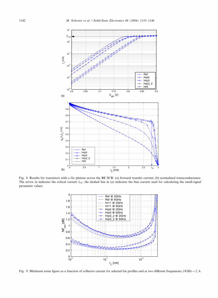
0.6 0.65 0.7 0.75 0.8 0.85 0.910
10
10
10
100
101
VBE
[V]
I C [m
A]
RefHrp0Hrp3Hrp3_2Hr6
ICK
0 0.5 1 1.5 2 2.5 30
0.1
0.2
0.3
0.4
0.5
0.6
0.7
0.8
0.9
1
IC
[mA]
g mV
T/I C [1
/V]
RefHrp0Hrp3Hrp3_2Hr6
ICK
(a)
(b)
−4
−3
−2
−1
Fig. 8. Results for transistors with a Ge plateau across the BE SCR: (a) forward transfer current; (b) normalized transconductance.
The arrow in indicates the critical current ICK ; the dashed line in (a) indicates the bias current used for calculating the small-signal
parameter values.
102
101
100
0
0.2
0.4
0.6
0.8
1
1.2
1.4
1.6
1.8
2
IC
[mA]
NF m
in [d
B]
Ref @ 2GHzRef @ 6GHzHr11 @ 2GHzHr11 @ 6GHzHrp0 @ 2GHzHrp0 @ 6GHzHrp3_2 @ 2GHzHrp3_2 @ 6GHz
Fig. 9. Minimum noise figure as a function of collector current for selected Ge profiles and at two different frequencies f /GHz¼ 2, 6.
1142 M. Schroter et al. / Solid-State Electronics 48 (2004) 1133–1146
M. Schroter et al. / Solid-State Electronics 48 (2004) 1133–1146 1143
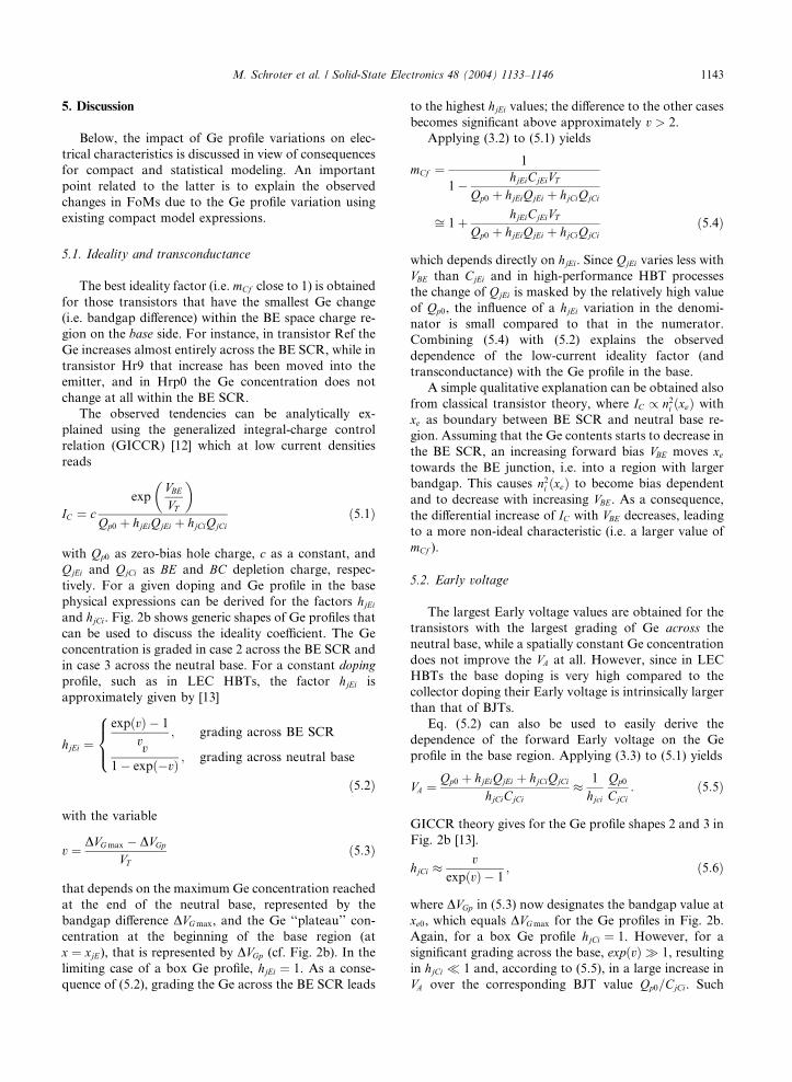
5. Discussion
Below, the impact of Ge profile variations on elec-
trical characteristics is discussed in view of consequences
for compact and statistical modeling. An important
point related to the latter is to explain the observed
changes in FoMs due to the Ge profile variation using
existing compact model expressions.
5.1. Ideality and transconductance
The best ideality factor (i.e. mCf close to 1) is obtained
for those transistors that have the smallest Ge change
(i.e. bandgap difference) within the BE space charge re-
gion on the base side. For instance, in transistor Ref the
Ge increases almost entirely across the BE SCR, while in
transistor Hr9 that increase has been moved into the
emitter, and in Hrp0 the Ge concentration does not
change at all within the BE SCR.
The observed tendencies can be analytically ex-
plained using the generalized integral-charge control
relation (GICCR) [12] which at low current densities
reads
IC ¼ cexp
VBEVT
� �Qp0 þ hjEiQjEi þ hjCiQjCi
ð5:1Þ
with Qp0 as zero-bias hole charge, c as a constant, and
QjEi and QjCi as BE and BC depletion charge, respec-
tively. For a given doping and Ge profile in the base
physical expressions can be derived for the factors hjEiand hjCi. Fig. 2b shows generic shapes of Ge profiles thatcan be used to discuss the ideality coefficient. The Ge
concentration is graded in case 2 across the BE SCR and
in case 3 across the neutral base. For a constant doping
profile, such as in LEC HBTs, the factor hjEi is
approximately given by [13]
hjEi ¼expðvÞ � 1
v; grading across BE SCR
v1� expð�vÞ ; grading across neutral base
8><>:
ð5:2Þ
with the variable
v ¼ DVGmax � DVGpVT
ð5:3Þ
that depends on the maximum Ge concentration reached
at the end of the neutral base, represented by the
bandgap difference DVGmax, and the Ge ‘‘plateau’’ con-
centration at the beginning of the base region (at
x ¼ xjE), that is represented by DVGp (cf. Fig. 2b). In the
limiting case of a box Ge profile, hjEi ¼ 1. As a conse-
quence of (5.2), grading the Ge across the BE SCR leads
to the highest hjEi values; the difference to the other casesbecomes significant above approximately v > 2.
Applying (3.2) to (5.1) yields
mCf ¼ 1
1� hjEiCjEiVTQp0 þ hjEiQjEi þ hjCiQjCi
ffi 1þ hjEiCjEiVTQp0 þ hjEiQjEi þ hjCiQjCi
ð5:4Þ
which depends directly on hjEi. Since QjEi varies less with
VBE than CjEi and in high-performance HBT processes
the change of QjEi is masked by the relatively high value
of Qp0, the influence of a hjEi variation in the denomi-
nator is small compared to that in the numerator.
Combining (5.4) with (5.2) explains the observed
dependence of the low-current ideality factor (and
transconductance) with the Ge profile in the base.
A simple qualitative explanation can be obtained also
from classical transistor theory, where IC / n2i ðxeÞ withxe as boundary between BE SCR and neutral base re-
gion. Assuming that the Ge contents starts to decrease in
the BE SCR, an increasing forward bias VBE moves xetowards the BE junction, i.e. into a region with larger
bandgap. This causes n2i ðxeÞ to become bias dependent
and to decrease with increasing VBE. As a consequence,
the differential increase of IC with VBE decreases, leadingto a more non-ideal characteristic (i.e. a larger value of
mCf ).
5.2. Early voltage
The largest Early voltage values are obtained for the
transistors with the largest grading of Ge across the
neutral base, while a spatially constant Ge concentration
does not improve the VA at all. However, since in LEC
HBTs the base doping is very high compared to the
collector doping their Early voltage is intrinsically larger
than that of BJTs.
Eq. (5.2) can also be used to easily derive the
dependence of the forward Early voltage on the Ge
profile in the base region. Applying (3.3) to (5.1) yields
VA ¼ Qp0 þ hjEiQjEi þ hjCiQjCi
hjCiCjCi� 1
hjci
Qp0
CjCi: ð5:5Þ
GICCR theory gives for the Ge profile shapes 2 and 3 in
Fig. 2b [13].
hjCi �v
expðvÞ � 1; ð5:6Þ
where DVGp in (5.3) now designates the bandgap value at
xe0, which equals DVGmax for the Ge profiles in Fig. 2b.
Again, for a box Ge profile hjCi ¼ 1. However, for a
significant grading across the base, expðvÞ 1, resulting
in hjCi � 1 and, according to (5.5), in a large increase in
VA over the corresponding BJT value Qp0=CjCi. Such
1144 M. Schroter et al. / Solid-State Electronics 48 (2004) 1133–1146
increases have been observed in drift-type SiGe HBTs
with conventional doping profiles.
Note that a reverse Early voltage can be calculated
similarly and is directly related to mCf .
5.3. Depletion capacitances
The larger the bandgap difference is between the
edges of the space-charge region the larger is the deple-
tion capacitance of a heterojunction; i.e. the variation in
the zero-bias depletion capacitances CjE0 and CjC0 is
caused by the variation of the bandgap at the SCR edges
on the p-and n-side of the respective junction. Thus, thearea specific zero-bias capacitance of a heterojunction
can be approximated by
C�j0 ffi Cj0
1
1� DVg;pn=VD0
� �1=z; ð5:7Þ
in which Cj0, VD0 and z, respectively, are the corre-
sponding area specific capacitance, built-in voltage, and
exponent factor, respectively, of the reference material
(e.g. Si) without intentional bandgap change but possi-
bly containing high-doping effects, while DVg;pn is the
intentional bandgap voltage difference at the depletion
region boundaries with respect to the reference material.
For instance, the higher CjE0 of transistor Hr9 compared
to transistor Hrp0 is due to the larger Ge contents at the
base-end of the BE SCR. Similarly, CjC0 of transistor
Hr6 decreases since the grading causes the bandgap at
the base-end of the BC SCR to already increase towards
the (Si) value in the collector.
5.4. Transit time and transit frequency
Two different operating regions need to be consid-
ered for discussing the variation in the transit frequency.
At low collector current densities, fT changes are causedmostly by changes of the depletion capacitances, while
at high current densities (peak and beyond) fT changes
are due to variations in the transit time. The fT peak
value is strongly correlated to the low-current transit
time sf0 which in LEC HBTs consists of a base com-
ponent sBf 0 and a BC SCR component sBC . The latter
depends very little on the Ge profile. The dependence of
sBf 0 on Ge changes can be examined using the general
equation [7]
sBf ¼Z wb
0
n2ip
Z wb
x
pVTlnn
2idx0
� �dx: ð5:8Þ
Since in LEC HBTs the base is highly doped (p ¼ NB)
the neutral base width as well as the electron mobility
are almost bias independent. According to (5.8), the
box profile (n2i ¼ constant) will not improve sBf 0 com-
pared to a BJT, so that the main reason for the higher
fT of the LEC HBT is the suppression of the emit-
ter minority charge. The variation observed for sf 0(cf. Table 1) with changing Ge slope at the BC junc-
tion is caused by the partial decrease of the Ge
concentration already in the metallurgical base region.
On the other hand, the sf 0 increase observed for
the positive Ge slope moving towards the emitter is
caused by an increasing minority charge in the base–
emitter transition region with the modified (lower)
bandgap.
The decrease of fT at high current densities is caused
by an increase in the transit time sf , once the electric
field at the BC junction has dropped to about Elim ¼ vs=lnC0, with vs as electron saturation velocity and lnC0 as
low-field mobility in the collector. Thus, the corre-
sponding critical current ICK that indicates the onset of
such high-current effects can still be determined from the
same theory as applied to BJTs (e.g. [8,14]). However, in
contrast to BJTs, the valence band barrier prevents holes
from entering the collector, but rather causes a dipole
layer to form [16] that acts as a retarding field for elec-
trons at the location where the Ge drops (e.g., at the BC
junction). The consequence is a rapid increase of the
electron density in the base, and the associated sf in-
crease can be modeled as described in, e.g. [15]. As a
computationally more simple and less physical ap-
proach, the presently existing equations in HICUM
[8,14] can still be used by assigning the sf increase pre-
dominantly to the base region rather than to the col-
lector region, i.e. setting the model parameter FTHC to
a very small value.
From both the fT and IC characteristics in Section 4,
it seems that for all transistors at high injection ICsaturates at the same current. This is due to the effects
described above. Calculating from the doping and
width of the collector the parameters entering the ICKequation used in [14] gives ICK ¼ 2:8 mA, which is a
reasonably good estimate for the onset of high current
and barrier effects (cf. Fig. 8). Compared to BJTs, fT (sf )at ICK has dropped (increased) to a smaller (larger) value
due to the additionally forming barrier for electrons,
which in HBTs causes a more rapid increase of the
electron charge with current density.
5.5. Current gain
The current gain depends strongly on both the Ge
concentration at (or before) the BE junction and the Ge
profile within the base. The first determines the barrier
for back injection of holes into the emitter, while the
latter determines the collector current. For statistical
modeling both variations need to be taken into account.
A ‘‘peaky’’ shape (i.e. a visible but relatively slow drop
towards higher current densities) of the low-injection
current gain can be caused by an increased non-ideality
factor due to Ge grading across the BE SCR (cf. earlier
M. Schroter et al. / Solid-State Electronics 48 (2004) 1133–1146 1145
discussion). At high current densities, the sharp current
gain drop is mostly due to the high-current effects dis-
cussed for the transit time and can be analytically
modeled as a function of the Ge contents via the GICCR
[12].
The current gain can be calculated from the ratio of
the (weighted) doping integrals of emitter and base.
Assuming that the difference of the (average) bandgap
reduction DV Ge;BE between base and emitter region, that
is due to the Ge contents, is entirely appearing in the
valence band, the bandgap dependence of the current
gain is roughly given by
B / expDV gB � DV gE
VT
� �
� expDV BGN ;B � DV BGN ;E þ DV Ge;BE
VT
� �; ð5:9Þ
where DV BGN ;B and DV BGN ;E are the average bandgap
reductions in base and emitter due to bandgap nar-
rowing. Since DV Ge;BE decreases with increasing Ge
contents in the emitter, B decreases, too, for e.g. tran-
sistors Hr8 and Hr9.
5.6. Minimum noise figure
Fig. 9 shows a comparison of the current dependent
minimum noise figure determined at 2 and 6 GHz. Note
that the calculated NFmin values in Table 1 and Fig. 9
indicate the trend and relative differences but not nec-
essarily the exact values achievable with the final pro-
cess. Overall, the Ge box profile turns out to be the best
choice, especially compared to the Ge profile with a long
plateau across the BE junction (in Hrp0). The difference
diminishes somewhat towards higher frequencies. It
seems though that for graded Ge profiles the minimum
of NFmin (like peak fT ) is shifted towards higher current
densities, where Hr11 yields slightly better results than
transistor Ref, but still with higher overall NFmin values.
Ge profiles similar to those in Ref, Hr6, Hr11, and
Hrp3_2 have also been investigated in [3] with respect
to high-frequency noise. While in our paper a similar
trend is obtained for Hr6 and Hrp3_2, the results for the
box and trapezoidal Ge profiles show the opposite ten-
dency. One reason for this observation can be the dif-
ferent doping profiles and maximum Ge mole fraction,
that influence the carrier transport and charge storage
at the end of the base and within both space-charge
regions.
6. Conclusions
SiGe HBT device designs with low-emitter doping
concentration have been investigated based on a realistic
reference doping and Ge profile. Case studies for the
sensitivity of important electrical characteristics and
typical process monitor values as a function of the Ge
profile have been performed. From a device design point
of view, the following conclusions can be drawn:
• The Ge profile design at the BC junction is of crucial
importance for transistor speed and Early voltage.
For a ‘‘useful’’ process, the Ge drop––even under
worst-case conditions––must always occur in the col-
lector. Otherwise, significant fT reductions (up to
50%) are possible. This assumption for a practically
‘‘useful’’ process allows significant simplifications in
statistical compact modeling.
• An aiding drift field in the base can significantly in-
crease the speed. For a given base–emitter doping
profile, an optimum mole fraction at the BE junction
and a maximum value of the Ge exist with respect to
speed, Early voltage, collector current ideality (i.e.
transconductance), and noise figure.
• A constant Ge contents across the BE SCR improves
the ideality (of IC and current gain) and transconduc-
tance especially at medium current densities for tran-
sistors with graded Ge profiles.
• The variation of the Ge profile slope at the BE junc-
tion has only a moderate impact on fT but can have alarge influence on the current gain.
• A reduction of a change in the maximum Ge mole
fraction has little impact on device performance, at
least for box-type profiles. There seems to exist an
optimum maximum mole fraction though.
Overall, for the given doping profile assumed in this
paper the optimum Ge profile seems to be close to
transistor Hrp3_2, possibly with a little lower Ge step at
the BE junction, a lower peak concentration to allow
some Ge extension into the collector for alleviating the
sharp drop in fT and current gain.
From a compact modeling point of view, the con-
clusions are
• the critical current density JCK , which indicates the
onset of high-current effects in the collector of homo-
junction bipolar transistors (BJTs) can still be used
for HBTs. However, the sf (fT ) value at JCK is for
SiGe HBTs usually larger (lower) than for BJTs
due to the barrier effect;
• the causes for the observed changes in electrical char-
acteristics can be explained from existing transistor
theory, mainly from GICCR and transit time theory;
• modeling the process tolerances due to a Ge drop al-
ready within the end of the base region should not be
relevant for statistical modeling of a practically use-
ful process;
• the simulated results are very useful for theory devel-
opment and extensions of HICUM specifically to-
wards the LEC HBT process type.
1146 M. Schroter et al. / Solid-State Electronics 48 (2004) 1133–1146
Additional transistors with ideal doping and Ge profiles
have been simulated to support and confirm the theo-
retical explanations for the observed variations in the
electrical characteristics.
The main differences between intrinsic conventional
and LEC HBTs are the shape and concentration of the
base and emitter doping. As a consequence, compared to
a conventional HBT the electrical behavior of LEC
HBTs is much more affected by the profiles within the
lightly doped emitter region. Furthermore, all presently
fabricated conventional SiGe HBTs known to the
authors have non-box base doping profiles with the
maximum of the boron concentration shifted towards
the BE junction, thus causing already a drift field for the
electrons towards the collector. Therefore, the shape of
the Ge profile within the base has a larger impact on the
intrinsic speed in LEC HBTs compared to conventional
SiGe HBTs.
Acknowledgements
The authors would like to thank J. Berntgen and L.
Kornau for providing process information and sup-
porting device simulations.
References
[1] Berntgen J et al. SiGe technology bears fruits. Mater Sci
Eng B 2002;89:13–20.
[2] Burghartz A et al. APCVD-grown self-aligned SiGe-base
HBTs. In: Proc IEEE Bipolar and BiCMOS Circuits and
Technology Meeting, 1993. p. 55–8.
[3] Ansley W, Cressler J, Richey D. Base-profile optimization
for minimum noise figure in advanced UHV/CVD SiGe
HBTs. IEEE Trans Microwave Theory Tech 1998;46:653–
60.
[4] Gruhle A. The influence of emitter–base junction design on
collector saturation current, ideality factor, early voltage
and device switching speed of Si/SiGe HBTs. IEEE Trans
Electron Dev 1994;41:198–203.
[5] Johnson J. Process and device simulation for SiGe
technology development. In: Short course at the IEEE
Bipolar and BiCMOS Circuits and Technology Meeting,
Minneapolis, 2001.
[6] Schr€oter M. Transient and small-signal high-frequency
simulation of numerical device models embedded in an
external circuit. COMPEL 1991;10(4):377–8;
see also: DEVICE––a mixed/mode device-circuit simula-
tor for DC, transient, and small-signal (hf) operation.
In: Proc NASECODE VII, Copper Mountain, USA, 1991.
p. 193–5.
[7] Kroemer H. Two-integral equations pertaining to the
electron transport through a bipolar transistor with non-
uniform energy gap in the base region. Solid-State Electron
1985;28:1101–3.
[8] Schr€oter M. HICUM, a geometry scalable physics-based
compact bipolar transistor model, December 2001. Avail-
able from: http://www.iee.et.tu-dresden.de/iee/eb.
[9] Gummel HK. On the definition of the cutoff frequency fT .Proc IEEE 1969;57:2159.
[10] Voinigescu S, Maliepaard M, Schr€oter M, Schvan P,
Harame D. A scaleable high-frequency noise model
for bipolar transistors and its applications in low-noise
amplifier design. IEEE J Solid-State Circuits 1997;32:
1430–9.
[11] Rein H-M. Proper choice of the measuring frequency for
determining fT of bipolar transistors. Solid-State Electron
1983;26:75–83, 929.
[12] Schr€oter M, Friedrich M, Rein H-M. A generalized
integral charge-control relation and its application to
compact models for silicon based HBT’s. IEEE Trans
Electron Dev 1993;40:2036–46.
[13] Schroter M, Tran H. Application of the generalized
integral-charge control relation to Si/SiGe bipolar transis-
tor compact modeling. To be submitted.
[14] Schr€oter M, Lee T-Y. A physics-based minority charge and
transit time model for bipolar transistors. IEEE Trans
Electron Dev 1999;46:288–300.
[15] Wilms S, Rein H-M. Analytical high-current model for the
transit time of SiGe HBTs. In: Proc IEEE Bipolar and
BiCMOS Circuits and Technology Meeting, 1998. p. 199–
203.
[16] Tiwari S. A new effect at high currents in heterostruc-
ture bipolar transistors. IEEE Electron Dev Lett 1988;9:
142–4.
Related Documents