Reprinted from NUCLEAR INSTRUMENTS & METHODS IN PHYSICS RESEARCH Section A Nuclear Instruments and Methods in Physics Research A 342 (1994) 83-89 North-Holland Gallium arsenide charged particle detectors; trapping effects RD8 Collaboration S.P. Beaumont d, R Bertin b, C.N. Booth i, C. Buttar i, L. Carraresi c, F. Cindolo a, M. Colocci c, F.H. Combley i, S. D'Auria a, C. del Papa a, M. Dogru i, M. Edwards -, F. Foster f, A. Francescato c, R Gray ', G. Hill '. Y. Hou i, P. Houston i, G. Hughes f, B.K. Jones f,*, J.G. Lynch e, B. Lisowski a, J. Matheson e, F. Nava g, M. Nuti c, V. O'Shea a, P.G. Peifer c, C. Raine c, J. Santana f, P.H. Seller h, K. Shankar c, P.H. Sharp ". 1.0. Skillicorn e, T. Sloan f, K.M. Smith e, N. Tartoni c, 1. ten Have e, RM. Turnbull e, U. Vanni c, A. Vinattieri c, K. Zdansky k, A. Zichichi b a Dipartimento di Fisica dell'Uniuersita and INFN, Bologna, Italy b CERN, Geneva, Switzerland C Dipartimento di Fisica dell'Unioersita and INFN, Florence, Italy d Department of Electrical and Electronic Engineering, University of Glasgow, UK e Department of Physici and Astronomy, University of Glasgow, UK f Department of Physics, University of Lancaster, UK e Dipartimento di Fisica dell'Unioersita and INFN, Modena, Italy h Rutherford Appleton Laboratory, Chilton, Didcot, Oxon, UK i Department of Physics, University of Sheffield, UK j Department of Electrical Engineering, University of Sheffield, UK k Institute of Radio-technology and Electronics, Prague, Czech Republic I ElSEVIER

Welcome message from author
This document is posted to help you gain knowledge. Please leave a comment to let me know what you think about it! Share it to your friends and learn new things together.
Transcript
Reprinted from
NUCLEARINSTRUMENTS&METHODSIN PHYSICSRESEARCH
Section A
Nuclear Instruments and Methods in Physics Research A 342 (1994) 83-89North-Holland
Gallium arsenide charged particle detectors; trapping effects
RD8 Collaboration
S.P. Beaumont d, R Bertin b, C.N. Booth i, C. Buttar i, L. Carraresi c, F. Cindolo a,M. Colocci c, F.H. Combley i, S. D'Auria a, C. del Papa a, M. Dogru i,M. Edwards -,F. Foster f, A. Francescato c, R Gray ', G. Hill '. Y. Hou i, P. Houston i, G. Hughes f,
B.K. Jones f,*, J.G. Lynch e, B. Lisowski a, J. Matheson e, F. Nava g, M. Nuti c, V. O'Shea a,P.G. Peifer c, C. Raine c, J. Santana f, P.H. Seller h, K. Shankar c, P.H. Sharp ".1.0. Skillicorn e, T. Sloan f, K.M. Smith e, N. Tartoni c, 1. ten Have e, RM. Turnbull e,U. Vanni c, A. Vinattieri c, K. Zdansky k, A. Zichichi b
a Dipartimento di Fisica dell'Uniuersita and INFN, Bologna, Italyb CERN, Geneva, SwitzerlandC Dipartimento di Fisica dell'Unioersita and INFN, Florence, Italyd Department of Electrical and Electronic Engineering, University of Glasgow, UKe Department of Physici and Astronomy, University of Glasgow, UKf Department of Physics, University of Lancaster, UKe Dipartimento di Fisica dell'Unioersita and INFN, Modena, Italyh Rutherford Appleton Laboratory, Chilton, Didcot, Oxon, UKi Department of Physics, University of Sheffield, UKj Department of Electrical Engineering, University of Sheffield, UKk Institute of Radio-technology and Electronics, Prague, Czech Republic
IElSEVIER
Nuclear Instruments and Methods-in Physics Research A 342 (1994) 83-89North-Holland
NUCLEARINSTRUMENTS& METHODSIN PHYSICSRESEARCH
Section A
Gallium arsenide charged particle detectors; trapping effects
RD8 Collaboration
S.P. Beaumont d, R Bertin b, C.N. Booth i, C. Buttar i, L. Carraresi c, F. Cindolo a,M. Colocci c, F.H. Cornbley i, S. D'Auria a, C. del Papa a, M. Dogru i, M. Edwards h,
F. Foster ', A. Francescato c, R Gray ', O. Hill '. Y. Hou '. P. Houston '. O. Hughes ',B.K Jones f,*, J.O. Lynch e, B. Lisowski a, J. Matheson e, F. Nava g, M. Nuti c, V. O'Shea a,
P.O. Pelfer c, C. Raine c, J. Santana '. P.H. Seller ''. K Shankar c, P.H. Sharp h,1.0. Skillicorn e, T. Sloan f, KM. Smith e, N. Tartoni c, 1. ten Have e, RM. Turnbull e,U. Vanni c, A. Vinattieri c, K Zdansky k, A. Zichichi b
a Dipartimento di Fisica dell'Uniuersita and INFN, Bologna, Italyb CERN, Geneva, SwitzerlandC Dipartimento di Fisica dell'Unioersita and INFN, Florence, Italyd Department of Electrical and Electronic Engineering, University of Glasgow, UKe Department of Physics and Astronomy, University of Glasgow, UKf Department of Physics, University of Lancaster, UKg Dipartimento di Fisica dell'Unioersita and INFN, Modena, Italyh Rutherford Appleton Laboratory, Chilton, Didcot, Oxon, UKi Department of Physics, University of Sheffield, UKj Department of Electrical Engineering, University of Sheffield, UKk Institute of Radio-technology and Electronics, Prague, Czech Republic
The progress on the development of gallium arsenide particle detectors is reviewed. The limitation to the performance is thepresence of traps. Studies of the trap properties using exparticle DLTS measurements and C-V measurements are described.
1. Introduction somewhat variable charge collection efficiencies. Theloss of charge collection efficiency has been attributedto the presence of traps in the material. In this paperwe describe work which is currently in progress toinvestigate the traps in the gallium arsenide materialand their effect on the design and properties of detec-tors.
In previous publications [1-4) we have demon-strated that it is possible to make charged particledetectors from gallium arsenide. Such detectors havebeen routinely made as microstrip devices as would berequired for a large area detector at the proposedLHC accelerator. Such a large area detector is cur-rently being designed for use by the ATLAS collabora-tion [5). The advantages of gallium arsenide over sili-con as a medium for charged particle detection are itsspeed due to the higher carrier mobility and its radia-tion hardness. The latter is a particular advantage inthe hostile, high radiation environment at the LHC.
In our previous publications [2-4) the speed and theradiation hardness of the devices were demonstrated.However, they -were found to be intrinsically morecomplicated than similar devices made in silicon with
The requirements of a detector include fast speed,high conversion efficiency and good radiation damageresistance. The fast speed can be obtained if the lengthof the depleted area is short and the carrier mobilities,or their saturation velocities if a high field can bedeveloped, are high. For a high conversion efficiencyfor minimum ionising particles the length of the de-pleted area should be long and all the free carrierscreated should leave this area rapidly. The damage
2. The detectors
* Corresponding author.
0168-9002/94/$07.00 © 1994 - Elsevier Science B.V. All rights reservedSSDI0168-9002(93)Ell18-H
I.DESIGN, FABRICATION
S.P. Beaumont et al. / Nucl. Instr. and Meth. in Phys. Res. A 342 (1994) 83-89
by radiation should not be such that the freecarriers are prevented from operating efficiently. Ofthe many practical considerations perhaps the mostrmportant are that the leakage current must be small50 that power dissipation is low and that any substrate,0: non-active thickness, is thin to reduce multiple scat-rermg and conversion of neutral particles.
Ideally the material would be very pure, with fewfree carriers and impurity levels, donors or acceptors,"fl:h a Schottky contact and an ohmic contact. Thepunry levels of GaAs are not high. In practice theavailable high resistivity material is semi-insulating andhas defects and impurities to form energy levels nearmid-gap which trap most free carriers. Commercialmaterial is variable in its properties since it is made fordevice substrate material and only simple inert charac-teristics are required for that use. The system is thuscomplex and one must be careful about the assump-tions made in even a device with a Schottky and anohmic contact.
The presence of deep levels, donor or acceptorenergy levels near mid-gap, can have several conse-quences. If full they can be ionised by the incomingradiation to release free carriers to create a signal. Ifempty they provide traps to capture the free carriers ofa signal to reduce the efficiency and if the free carriers31"ethen released slowly they can lengthen the signalpulse. Their charge state, or occupation, also alters thedepletion region width and hence the active volumeand the details of the charge capture.
Although it has been demonstrated that these de-
-9xl0 a
~ 0.1
~ 0.09
§ 0.08
0.07
0.06
0.05
0.04
0.03
0.02
0.010 20 40 100
REVERSE BIAS (V)
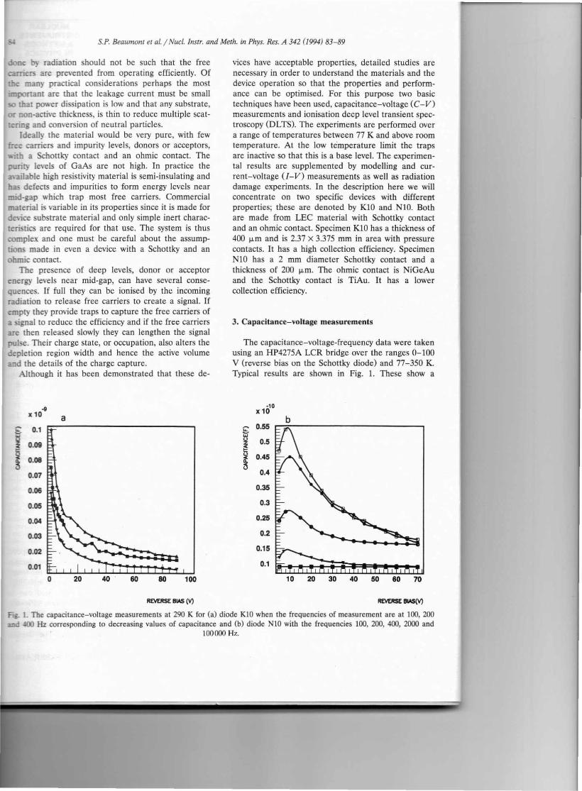
vices have acceptable properties, detailed studies arenecessary in order to understand the materials and thedevice operation so that the properties and perform-ance can be optimised. For this purpose two basictechniques have been used, capacitance-voltage (C-V)measurements and ionisation deep level transient spec-troscopy (DLTS). The experiments are performed overa range of temperatures between 77 K and above roomtemperature. At the low temperature limit the trapsare inactive so that this is a base level. The experimen-tal results are supplemented by modelling and cur-rent-voltage (I-V) measurements as well as radiationdamage experiments. In the description here we willconcentrate on two specific devices with differentproperties; these are denoted by KlO and NlO. Bothare made from LEe material with Schottky contactand an ohmic contact. Specimen KlO has a thickness of400 urn and is 2.37 X 3.375 mm in area with pressurecontacts. It has a high collection efficiency. SpecimenNIO has a 2 mm diameter Schottky contact and athickness of 200 urn, The ohmic contact is NiGeAuand the Schottky contact is TiAu. It has a lowercollection efficiency.
3. Capacitance-voltage measurements
The capacitance-voltage-frequency data were takenusing an HP4275A LCR bridge over the ranges 0-100V (reverse bias on the Schottky diode) and 77-350 K.Typical results are shown in Fig. 1. These show a
·10xl0
~ 0.55I;:j'
~0.5
~0.45
0.4
0.35
0.3
0.25
0.2
0.15
0.1
10 20 30 40 50 60 70
REVERSE 8IAS(V)
fig. 1. The capacitance-voltage measurements at 290 K for (a) diode KI0 when the frequencies of measurement are at 100, 2003Ld 400 Hz corresponding to decreasing values of capacitance and (b) diode N10 with the frequencies 100, 200, 400, 2000 and
100000 Hz.

S.P. Beaumont et al. / Nucl. Instr. and Meth. in Phys. Res. A 342 (1994) 83-89
decrease as the voltage increases, corresponding to anincrease in the depletion width. There is a large fre-quency dependence at this temperature with a de-crease in the capacitance (increase in depletion width)as the frequency increases. As the temperature in-creases the capacitance increases as the depletion widthdecreases.
Although the system is complex and corrections areneeded, a simple and consistent approximate analysisof the main features can be made by assuming that thematerial is a simple n-type semiconductor. This modelcan then be extended to include several trapping levels.
With this assumption the capacitance per unit areafor a Schottky diode made of a semiconductor withuniform carrier concentration n
(1)
where d is the depletion width, €r€O the dielectricconstant and Vbi the built-in voltage. For a semicon-ductor with a significant number of deep impuritylevels the quantity measured is not equal to the carrierdensity, n, or the ionised donor density but someeffective space charge Neff' At small voltages this is ofless importance. We also assume no current flow. Re-arranging this gives
(2)
so that the slope of the 1jC2-V curve gives the carrierconcentration.
A typical curve of 1jC2-V at low voltage is shownin Fig. 2. It can be seen that these could be straightline sections with decreasing slope as the depletion isincreased. We will return to this later. If we use Eq. (1)we can obtain a plot of the depletion width againstvoltage and this is shown in Fig. 3 over a larger rangeof bias voltage for the two specimens. It can be seenthat the slopes and the absolute values vary betweenspecimens depending on the material and the trapdetails.
The significant feature of traps is that they fill at a.rate, usually fast, dependent on the free carrier densityand the trap cross-section, (J', and they empty by ther-mal activation to the conduction (or valence) band at arate given by the Boltzmann factor exp( - EAj kT),where EA is the trap energy depth. Each trap there-fore has a characteristic response time, T. If the mea-surement is performed at a slower rate the trap re-sponds, if at a faster rate then it is inactive. As thetemperature is changed different traps will becomeactive at the experimental frequency or, if the experi-ment is kept at one temperature, the traps becomeactive as the experimental frequency is changed. Fig. 4shows a typical plot of dVjd(ljC2), taken at a low
,.....7:,
2.3[t' 2.275<,
2.25
2.225
2.2
2.175
2.15
2.125
2.1
•
REVERSE BIAS (V)
Fig. 2. The plot of I/C2 against voltage V for specimen KIOat 290 K and frequencies 100, 200, 400 Hz corresponding todecreasing values of capacitance. The reciprocal slope mea-
sures the carrier density.
applied voltage, against the measurement frequencyand a fit to the Debye curve which is expected. Thefrequency of the transition gives the characteristic traptime and the amplitude between the low and highfrequency limits gives a measure of the number ofactive traps via Eq. (1). The fit to theory is good andthe apparent number of traps is constant with tempera-ture, which gives confidence in the analysis. These datawill be presented later and compared with values ob-tained by DLTS. This frequency analysis means that
LOG REVERSE BIAS(V)
Fig. 3. Depletion width against voltage at 290 K for diodesKlO (e) and NIO (.).
1. DESIGN, FABRICATION
85

0.3
86 S.P. Beaumont et al. / Nucl. Instr. and Meth. in Phys. Res. A 342 (1994) 83-89
frequency and temperature are related variables andconsiderable time can be saved by taking data at onlyone frequency. The basic features of the results in Fig.1 can now be understood. It should be noted thatbecause of the large effect of traps the speed at whichall measurements, of all quantities, are made needs tobe stated as well as the temperature so that it can beknown which traps are active.
We will now return to the 1/C2-V curve of Fig. 2and discuss the changes of slope as the voltage in-creases. This corresponds to apparent increases in thecarrier density. For this material it is expected thatthere will be several deep and shallow levels and this isverified by the measurements presented here and later.This results in a complicated structure for the bandsbent in the semiconductor depletion region. Aschematic diagram is shown in Fig. 5 for the case ofone electron trap and one shallow donor.It can be seen that the bands are bent so that the
different traps intersect the Fermi energy at differentdepths into the semiconductor. The trap is assumed tobe donor-like and it is full and uncharged if it is belowthe Fermi energy but is charged if above. Each trap hasits own characteristic time depending on its energydepth and the temperature. The basic structure is oneof layers parallel to the metal electrode with the layerscontaining more trap levels ionised as they are closerto the metal. We thus see the. basic features of ourresults. As the frequency or temperature is changedthe traps which contribute may change from those atthe edge of one of these layers to include those at
7" 0.65E.p'0 0.6-7'~ 0.55<,~'i 0.5.,......N 0.45....,
0.4
0.35
LOG FREQUENCY (Hz)
Fig. 4. The variation of dVjd(ljC2) with frequency forspecimen KID at temperatures of 290,310 and 340 K and 1 V.The curves are fits to the Debye function, 1(1+ ",2'1'2), wherew is the measurement of frequency and '1' is the trap charac-
teristic time constant.
Electrontenergy ;1
Metal
-------Ey
f . e(Nt +'1t)u......-------.J e(Nd)-Charge
density
Distance_
Fig. 5. A schematic diagram of the bands bent at the Schottkydiode boundary. It is drawn for a shallow donor and one deepdonor trap. The shaded areas of the charge density representthe charge taking part in the AC capacitance measurement if
the trap can respond.
another edge, with a different density. Similarly at onefrequency and temperature one trap will be active atlow voltages. As the voltage is increased the bandsbend and successive layers form with more trapsionised. This alters the internal field distribution andthe capacitance and depletion width voltage curves[6,7].
This C-V measurement also has the potential fordetermining the number and properties of the trapsfrom the breaks and slopes. However the analysis isnot straightforward and the experiment is complicatedby the presence of three characteristic frequencies: theAC modulation of the capacitance measurement, theramp rate of the C-V data and the time the specimenhas had to reach equilibrium in its trap occupationafter any change in the conditions.
4. DLTS measurements
Deep level transient spectroscopy (DLTS) is a wellestablished technique to study the properties of traps.There are many possible variants depending on thesample being studied. In the basic technique the trapsare filled by moving the Fermi level or by some otherexcitation and then some property of the sample, suchas the conductance or depletion capacitance, is moni-tored as the traps empty by thermal excitation. Theamplitude of the transient gives a measure of thenumber of traps while the temperature dependence ofthe time constant gives the activation energy EA andthe trap cross-section, a .

SP. Beaumont et al. / Nucl. Instr. and Meth. in Phys. Res. A 342 (J994) 83-89
ideal behaviourOtt) trapless diode ...... 2.25;;
0._..2w
0
E 1.75..Ja.~ 1.5w~ 1.25:>a.
0.25
0.75
......................
time
0.5Bias supply
1 MOhm IntegratingAmplifier
~Digital1 pF Scope
o 0.1 0.2 0.3 0.4 0.5 0.6 0.7 0.8 0.9X 19.5
TIME (.)Fig. 7. A typical charge transient pulse from the circuit of Fig.6. Specimen KlO at 290K using e-particle excitation into the
Schottky contact end of the diode.
particles-Detector
Fig. 6. The circuit diagram of the (X·DLTSmeasuring circuitand a schematic diagram of the transient seen in the charge
amplifier. The device is biased as a particle detector undercurrent bias and the signal is passed into an integratingamplifier to produce a charge pulse. The circuit isshown in the inset to Fig. 6 which also shows the signalobtained. For an ideal device and amplifier there is arapid rise after the incoming radiation pulse and thecharge level remains constant. With real amplifiers theoutput droops over long times. The rise time is deter-mined by the transit time of the ionised carriers andthe amplifier response time. In our detectors a compo-nent of the rise is exponential and determined by some
The depletion capacitance transient can be studiedbut normally for devices made from semi-insulatingmaterial the transient in the device conductance isstudied after an optical pulse to excite the carriers. Wehave developed a new technique which has the advan-tage of being very versatile and also reflecting theparticle detection capabilities to which the devices be-ing studied will be used.
......~ /... a b~ 14 14
C c..J ..J
12 12
10 10
8 8
6 /' 6 /'4 4
2 I / 2 ///0 0
·2 JLL11l1 11 1 I I I I I I I I I I ·2 II I I I _l 1_l 1 I I2 4 6 8 10 12 2 4 6 8 10 12
1000/T(K) 1000/T(K)
Fig. 8. The Arrhenius plot for the traps seen in the diodes. The solid lines are from the DLTS experiments, the broken lines arefrom the C-V data and the data points are from the recovery time constant. (a) diode KIO, (b) diode NIO.
I.DESIGN, FABRICATION
87

88 S.P. Beaumont et al.j Nucl. lnstr. and Meth. in Phys. Res. A 342 (1994) 83-89
10OO/T (K) 1000/T(K)
Fig. 9. The trap concentrations found using the C - V data for the traps shown in Fig. 8. (a) diode KlO, (b) NIO. The concentrationof the trap providing the recovery time constant (shaded region) was deduced from the DLTS data.
trap time constant. This trapping slows the response,and if slow compared with the amplifier droop, reducesthe pulse height and hence the detector efficiency. Atypical experimental curve is shown in Fig. 7.
We fit the response to a function of the form
A = {Ao+ LAHl-exp( -At)]} exp(-A3t), (3)t
where Ao is the primary ionisation step, Al is theamplitude proportional to the number of traps, (A2)-1
is the trap time constant and (A3)-1 is the amplifierdroop time constant which does not vary during theexperiment. A number, i, of traps can be fitted.
At low temperatures no traps are active but as thetemperature is raised the traps speed up to becomefaster than the amplifier droop rate and hence becomemeasurable. At higher temperatures they become fasterthan the amplifier rise time and then add to the fastprimary response Ao so that the charge collectionefficiency increases. From the temperature depend-ence of the trap transients we can obtain the trapactivation energy EA and cross section, (J'.
The Arrhenius plot for the C-V and DLTS data isshown in Fig. 8a for specimen KlO and in Fig. 8b forspecimen NlO.
It can be seen that there is excellent agreementbetween the two methods for EA (the slope of thecurve) and (J' (the intercept). These measurements thushave the capability of completely characterising thetraps within the devices. Modelling of the band bend-ing is then possible using these data in Poisson's equa-tion.
The trap densities for the same specimens mea-sured using the C-V method are shown in Fig. 9.
These DLTS results were obtained by using a-par-ticles injected into the Schottky gate side. The smalldepth of penetration results in the ionisation occurringin the depletion region. Data have been obtained withthe a's injected through the ohmic contact. Measure-ments are in progress using minimum ionising signalsfrom a (3 source. Short light pulses with photon energyabove and below the band gap energy, so that there isshort and deep penetration, have also been used todemonstrate the versatility of the technique and toverify the ionising radiation results. There is completeconsistency.
The results of all these measurements are sum-marised in Table 1 which shows the trap parametersand possible trap identification [8,9]. It appears that
Table 1Measured properties of the traps found from the C - V data
Trapenergy (eV)
Capture crosssection (cm-2)
LabelTrapdensity (em -3)
KIO; CCE for alphas 80% at room temperature0.70 1.6E-14 1.65E16 EL20.61 1.9E-10 2.01E150.24 7.12E-16 7.2E14
NIO; CCE for alphas 30% at room temperature0.70 1.6E-14 1.9E16 EL20.62 2.07E-I0 1.91E150.32 4.2E- 15 1.2El5 ET20.119 l.32E -17 7E14

S.P. Beaumont et al. / Nucl. Instr. and Meth. in Phys. Res. A 342 (1994) 83-89
the low efficiency and other undesirable propertiesshown by NlO is due to the lower-energy traps, sincethese are the observed difference between it and thegood diode KlO.
We would like to report an encouraging result whichsuggests that samples with poor efficiency, and perhapsthose that have had their performance degraded byradiation damage, may have their efficiency increased.At low temperatures a device showing an efficiency ofabout 70% can be treated to give a nearly ideal charac-teristic with approaching 100% efficiency by applying ashort forward bias pulse to fill all the traps.
The inefficiency recovers with an exponential timeconstant corresponding to a trap. This time constant isplotted on the Arrhenius plot of Fig. 8b. This is thusevidence that trap removal, compensation or filling canbe used to improve the device performance. The accu-racy of the recovery data using this present method isnot yet high enough to identify the trap involved.
5. Discussion
The results presented show that GaAs detectorshave an acceptable performance. However there arestill aspects of devices made from a maturing technol-ogy which require investigation to aid understanding sothat consistent high quality and reliable devices may befabricated. One aspect is the need to understand andcharacterise the material which is needed for the fabri-cation and can be expected to be available.
The results presented here for the analysis andmeasurement of the properties of the traps in thedevices show that much is known about the traps in thelow temperature region. However there are no obviousexplanations available for some of the effects seen in
the specimens at room temperature and above, wherethe devices will be expected to work.
The C-V results at room temperature for somespecimens, with poor efficiency, show a capacitancemaximum at very low voltages. This is shown in Fig. lb.The trap densities measured from the a-DLTS tran-sients also show unexpected variations near room tem-perature in the same samples. The behaviour of thesesamples needs to be understood so that all devices canbe made to the standard of the good devices.
Acknowledgements
We wish to thank SERe (UK) and INFN (Italy) forfinancial support.
References
[1] R. Bertin et al., Nuci. Instr. and Meth. A 294 (1990) 211.[2] S.P. Beaumont et ai., Nucl. Instr. and Meth. A 321 (1992)
172.[3] S.P. Beaumont et aI., Nucl. Instr. and Meth. A 322 (1992)
472.[4] S.P. Beaumont et aI., Nucl. Instr. and Meth. A 326 (1993)
313.[5] ATLAS Letter of Intent CERN LHCC 92/4 LHCC/12
(1992).[6] P. Blood and J.W. Orton, Electrical Characterisation of
Semiconductors: Majority Carriers and Electron States(Academic Press, 1992).
[7] Z. Li and H.W. Kraner, IEEE Trans. Nucl. Sci. NS-38(1991) 244.
[8] G.M. Martin, A. Mitonneau and A. Mircea, Electron.Lett. 13 (1977) 191.
[9] A. Mitonneau, G.M. Martin and A. Mircea, Electron.Lett. 13 (1977) 666.
I. DESIGN, FABRICATION
89
I!
II
Ii
Ii
II
•
Related Documents