Process Development and Device Modelling of Gallium Arsenide Heterojunction Bipolar Transistors Anssi Hovinen Dissertation for the degree of Doctor of Science in Technology to be presented with due permission for public examination and debate in Auditorium S4 at Helsinki University of Technology (Espoo, Finland) on the 1 st of June, 2001, at 12 o’clock noon. Helsinki University of Technology Department of Electrical and Communications Engineering Electron Physics Laboratory Teknillinen korkeakoulu Sähkö- ja tietoliikennetekniikan osasto Elektronifysiikan laboratorio

Welcome message from author
This document is posted to help you gain knowledge. Please leave a comment to let me know what you think about it! Share it to your friends and learn new things together.
Transcript
Process Development and Device Modelling of Gallium
Arsenide Heterojunction Bipolar Transistors
Anssi Hovinen
Dissertation for the degree of Doctor of Science in Technology to be presented with duepermission for public examination and debate in Auditorium S4 at Helsinki Universityof Technology (Espoo, Finland) on the 1st of June, 2001, at 12 o’clock noon.
Helsinki University of TechnologyDepartment of Electrical and Communications EngineeringElectron Physics Laboratory
Teknillinen korkeakouluSähkö- ja tietoliikennetekniikan osastoElektronifysiikan laboratorio

A. Hovinen: Process Development and Device Modelling of Gallium Arsenide Heterojunction Bipolar...
Helsinki University of Technology Electron Physics Laboratory
i
Distribution:
Helsinki University of Technology
Electron Physics Laboratory
P.O. Box 3000
FIN-02015 HUT
Finland
Tel. +358-9-451-2322
Fax. +358-9-451 5008
ISBN 951-22-5438-7
ISSN 0781-4984
Otamedia Oy
Espoo 2001

HELSINKI UNIVERSITY OF TECHNOLOGYP.O. BOX 1000, FIN-02015 HUT
http://www.hut.fi
ABSTRACT OF DOCTORAL DISSERTATION
Author
Name of the dissertation
Date of manuscript Date of the dissertation
Monograph Article dissertation (summary + original articles)
Department
Laboratory
Field of research
Opponent(s)
Supervisor
(Instructor)
Abstract
Keywords
UDC Number of pages
ISBN (printed) ISBN (pdf)
ISBN (others) ISSN
Publisher
Print distribution
The dissertation can be read at http://www.hut.fi/Yksikot/Kirjasto/Diss/

A. Hovinen: Process Development and Device Modelling of Gallium Arsenide Heterojunction Bipolar...
Helsinki University of Technology Electron Physics Laboratory
ii
Abstract
This thesis discusses the processing and analysis of high speed semiconductor devices with
emphasis on GaAs-based heterojunction bipolar transistors. The heterojunction transistor
process is developed as an essential part of this thesis. Device physics is first reviewed in depth
to construct a solid basis for physical one dimensional simulation of heterojunction bipolar
junction transistors. Theory is then applied to a simulation platform in a way which facilitates
device design and evaluation at practical level. The simulation platform was used in designing
epitaxial layers for a transistor structure with heavily doped base layer and current gain target at
50. The developed transistor process relies on wet chemical isolation etching, and takes into
account the restrictions that arise from the academic perspective of the processing environment.
The process development goal was educational robustness.
The development effort for HBT process is explained in detail, and processing steps are
illustrated with scanning electron microscope images. The most critical processing steps were
for defining isolation depths. Isolation is based on slow citric acid wet chemical etching
monitored with a high precision profilometer. Active devices form isolated hills or “mesas” on
the semi-insulating substrate. Because of the rather tall etched structures the lithography is of
planarizing type. The process includes a unique double layer planarising lithography for AZ
5214E resist, developed within the framework of this thesis. The lithography is doubly
functional such that it also allows two resist layers to be patterned separately on top of each
other, which is utilised in defining shallow air bridges in the transistor structures.
The most important measurement results are explained. Degradation of transistor performance
after excessive heating or current stress is also demonstrated, and a method for processing
devices with minimal amount of heating is introduced as a means to takcle the problem.
Measured collector characteristics of various types of HBTs are given. Best DC characteristics
were achieved with a transistor structure including non-alloyed contacts and Schottky diode
collector. This thesis focused on process development and DC analysis of the transistor.
Frequency characteristics were measured only for completeness. It is shown that even the non-
optimized process was capable of producing transistors with power gain cut off frequency
exceeding 1 GHz.
Keywords: heterojunction, aluminum gallium arsenide, simulation, low thermal
budget, double layer lithography, process development

A. Hovinen: Process Development and Device Modelling of Gallium Arsenide Heterojunction Bipolar...
Helsinki University of Technology Electron Physics Laboratory
iii
Preface
Laboratory scale process development using compound semiconductors as starting material
may be an endless source of inspiration and joy for a researcher. For another, it may become a
nightmare. Processing steps on gallium arsenide are demanding. Samples may be extra fragile
with appreciable price tag. Proper way of doing the job is crucial. In laboratory scale efforts,
process development on compound semiconductors turns very easily into learning by doing
mistakes. Picking up tweezers of wrong material would be a mistake. Using force would be
another. For that matter, any treatment other than predetermined by the process schedule on the
sample would be a provocation towards pain. It becomes obvious that completion of any
process run on gallium arsenide is next to heroic as compared to silicon processing.
I have been privileged to have the opportunity to practise compound semiconductor research for
several years with Electron Physics Laboratory of Helsinki University of Technology. The
laboratory offers facilities for both silicon and compound semiconductor processing studies.
My generation of students was the last to enjoy the famous Old Clean Room of Wing C with its
3” MOS line. Today, our students in the semiconductor field may have more modern equipment
in their new clean rooms, but perhaps because of that may also start to loose the inspiring touch
of the pioneering atmosphere that once was among the new comer trying to wade through the
very first steps of semiconductor practise. I thank my supervisor, Professor Pekka Kuivalainen,
and the Head of Electron Physics Laboratory, Professor Juha Sinkkonen for my education in
semiconductor physics, devices and technology in the way which respects our civilizational
history of technology as much as the modern aspects of semiconductor research.
This work has benefitted from the input of numerous individuals. Some of them are introduced
in Chapter 6, Acknowledgements. After all, the most valuable criticism about the substance of
this work was supplied by my children and my wife, with their justified arguments about
occupying their gaming platforms with my Matlab simulations and text editors.

A. Hovinen: Process Development and Device Modelling of Gallium Arsenide Heterojunction Bipolar...
Helsinki University of Technology Electron Physics Laboratory
iv
List of Symbols
A* Richardson constant
A First coefficient of the Joyce-Dixon approximation
B Second coefficient of the Joyce-Dixon approximation
C Third coefficient of the Joyce-Dixon approximation
D Fourth coefficient of the Joyce-Dixon approximation
D(x) Electric flux
D(X) Transparency function with argument X
D0(X) Transparency function of an abrupt junction with argument X
Dn Minority carrier diffusion coefficient in n-type semiconductor
Dnb Electron diffusion coefficient in base
Dp Minority carrier diffusion coefficient in p-type semiconductor
Dpc Hole diffusion coefficient in collector
Dpe Hole diffusion coefficient in emitter
E0 Vacuum energy level
E00 Activation energy of tunneling through a Schottky barrier
E* Lower boundary of integration for transparency calculation
Ec Energy level of the bottom of conduction band
Ef Fermi level of energy
Ef1 Fermi level of base layer
Ef2 Fermi level of emitter layer
Eg Width of the forbidden band gap in energy
Eg,emitter Width of the forbidden band gap in energy of emitter
Eg1 Width of the forbidden band gap in energy of p-side of the junction
Eg2 Width of the forbidden band gap in energy of n-side of the junction
Eg,base Width of the forbidden band gap in energy of base
Eg,collectorWidth of the forbidden band gap in energy of collecotr
Em,abrupt Energy difference between conduction band tip level and conduction band edge of
neutral AlGaAs in an abrupt heterojunction
Em,graded Energy difference between conduction band tip level and conduction band edge of
neutral AlGaAs in a graded heterojunction

A. Hovinen: Process Development and Device Modelling of Gallium Arsenide Heterojunction Bipolar...
Helsinki University of Technology Electron Physics Laboratory
v
Ev Energy level of the top of valence band
∆Ec Conduction band energy difference
∆Eg Amount of the change in band gap width
∆Ev Valence band energy difference
F1/2 Fermi-Dirac integral
F(x) Electric field
fN Joyce-Dixon approximation function for n-type semiconductor
fP Joyce-Dixon approximation function for p-type semiconductor
h Plank’s constant
IB Base current
IE Emitter current
IC Collector current
J0 Saturation current density
J12* Electron current density from GaAs to AlGaAs of abrupt heterojunction due to Schottky
junction analogy
J21* Electron current density from AlGaAs to GaAs of abrupt heterojunction due to Schottky
junction analogy
Jb Total base current density
Jc Total collector current density
Jc,diff Collector diffusion current density
Jc,drift Collector drift current density
Je Total emitter current density
JgC Base-collector depletion region generation current density
Jn Total electron current density across AlGaAs/GaAs junction
Jnb Electron current density from GaAs to AlGaAs
Jnf Electron current density from AlGaAs to GaAs
Jne Emitter electron current density
JNE Coefficient for the calculation of emitter electron current density
Jp Hole current density
JPC Coefficient for the calculation of collector hole current density
Jpe Emitter hole current density
JPE Coefficient for the calculation of emitter hole current density

A. Hovinen: Process Development and Device Modelling of Gallium Arsenide Heterojunction Bipolar...
Helsinki University of Technology Electron Physics Laboratory
vi
Jr Neutral base layer recombination current density
Jre Emitter-base depletion region recombination current density
JShockley Current density of a pn-junction diode due to Shockley
Jsm Current density from the flow of electrons from semiconductor to metal
J*thermionic emission Total current density of abrupt heterojunction due to Schottky junction
analogy
k Boltzmann constant
K Ratio of the permittivity-doping density product of either side of the junction
Ln Minority carrier diffusion length in n-type semiconductor
Lnb Electron diffusion length in base
Lp Minority carrier diffusion length in p-type semiconductor
Lpc Hole diffusion length in collector
Lpe Hole diffusion length in emitter
Mc Number of equivalent minima of the conduction band
mde Density of states effective mass of electron
mdh Density of states effective mass of hole
me* Conductivity effective mass of electron
me1* Conductivity effective mass of electron in base layer
n Free electron concentration
∆n Excess electron density
n0 Thermal equilibrium electron concentration in p-type semiconductor
n0b Thermal equilibrium electron concentration in base layer
N+ Density of ionized donors
N - Density of ionized acceptors
NA Acceptor doping density
NB Base doping density
nc Mobile electron concentration in collector depletion region
NC Collector doping density
Nc Conduction band density of states
Ncb Conduction band density of states of base layer
Ncc Conduction band density of states of collector layer
Nce Conduction band density of states of emitter layer

A. Hovinen: Process Development and Device Modelling of Gallium Arsenide Heterojunction Bipolar...
Helsinki University of Technology Electron Physics Laboratory
vii
ND Donor doping density
NE Emitter doping density
nhot Concentration of electrons with enough energy to surmount the conduction band spike
by thermionic emission
ni Intrinsic carrier concentration
ni1 Intrinsic carrier concentration of p-side of the junction
ni2 Intrinsic carrier concentration of n-side of the junction
np Minority electron concentration
np0 Minority electron equilibrium concentration
Nt Trap state density
Nv Valence band density of states
Nvb Valence band density of states of base layer
Nve Valence band density of states of emitter layer
Nvc Valence band density of states of collector layer
p Free hole concentration
∆p Excess hole density
p0 Thermal equilibrium hole concentration in n-type semiconductor
p0c Thermal equilibrium hole concentration in collector layer
p0e Thermal equilibrium hole concentration in emitter layer
Rth0 Thermal resistance of the substrate
q Unit charge
Q Total charge density of the base layer
Rn Simplifying coefficient without dimension used in excess electron density calculation
Rp Simplifying coefficient without dimension used in excess hole density calculation
T Device temperature
U Recombination rate
V(x) Potential
Va Applied potential
Va1 Portion of applied potential over the p-side of the junction
Va2 Portion of applied potential over the n-side of the junction
Vbc Applied voltage over base-collector junction
VBE Potential difference between base terminal and emitter terminal
Vbe Applied voltage over base-emitter junction

A. Hovinen: Process Development and Device Modelling of Gallium Arsenide Heterojunction Bipolar...
Helsinki University of Technology Electron Physics Laboratory
viii
Vbi Built-in potential
Vb1 Portion of built-in potential over base side depletion region
Vb2 Portion of built-in potential over emitter side depletion region
Vcb Potential difference between collector terminal and base terminal
Vce Potential difference between collector terminal and emitter terminal
Vj Potential over the junction
Vj1 Portion of junction potential over the p-side
Vj2 Portion of junction potential over the n-side
Vjc Potential over base-collector junction
Vje Potential over base-emitter junction
vn* Richardson-Dushman velocity
vs Electron saturation velocity
vth Thermal velocity of electrons
Wbase Neutral region thickness of base layer
Wemitter Neutral region thickness of emitter layer
Wcollector Neutral region thickness of collector layer
WdC Width of the base-collector junction depletion region
Wgr Width of the grading layer of graded heterojunction
x AlAs mole fraction
X Argument of the transparency function
XB p-layer thickness of a long diode
XC Coordinate of the collector side edge of the base-emitter junction depletion region
XE n-layer thickness of a long diode
X1 Coordinate of the base side edge of the base-emitter junction depletion region
X2 Coordinate of the emitter side edge of the base-emitter junction depletion region
X3 Coordinate of the base side edge of the base-collector junction depletion region
X4 Coordinate of the collector side edge of the base-emitter junction depletion region
Xje Coordinate of the base-emitter metallurgical junction
Xjb Coordinate of the collector contact junction
Xjc Coordinate of the base-collector metallurgical junction
β Large signal current gain
γ Emitter injection efficiency

A. Hovinen: Process Development and Device Modelling of Gallium Arsenide Heterojunction Bipolar...
Helsinki University of Technology Electron Physics Laboratory
ix
ε0 Permittivity of vacuum
εr Permittivity relative to vacuum
εs Permittivity of the semiconductor
εs1 Permittivity of the base layer
εs2 Permittivity of the emitter layer
εs3 Permittivity of the collector layer
ηn Simplifying coefficient without dimension used in excess electron density calculation
ηp Simplifying coefficient without dimension used in excess hole density calculation
Θ1 Energy difference between Fermi level and GaAs valence band edge
Θ2 Energy difference between AlGaAs conduction band edge and Fermi level
σ Capture cross section of a trap state
σn Electron capture cross section of a trap state
σp Hole capture cross section of a trap state
τ Minority carrier lifetime
τn Electron lifetime in p-type semiconductor
τp Hole lifetime in n-type semiconductor
φB Schottky barrier height
φB* Energy difference between Fermi level and the tip of conduction band spike

A. Hovinen: Process Development and Device Modelling of Gallium Arsenide Heterojunction Bipolar...
Helsinki University of Technology Electron Physics Laboratory
x
Abbreviations
Al Aluminum
AlAs Aluminum arsenide
AlGaAs Aluminum gallium arsenide
AlN Aluminum nitride
As Arsene
ASCII American Standard Code for Information Interchange
BJT Bipolar Junction Transistor
CPE Chemical plasma etching
Ga Gallium
GaAs Gallium arsenide
GaAsSb Gallium arsene antimonide
GaN Gallium nitride
HBT Heterojunction Bipolar Transistor
HEMT High Electron Mobility Transistor
In Indium
InGaAs Indium Gallium Arsenide
InGaP Indium Gallium Phosphide
InP Indium phosphide
MBE Molecular Beam Epitaxy
MOCVD Metallo-Organic Chemical Vapor Deposition
MOVPE Metallo-organic Vapor Phase Epitaxy
PECVD Plasma enhanced chemical vapor deposition
RBS Rutherford Back Scattering

A. Hovinen: Process Development and Device Modelling of Gallium Arsenide Heterojunction Bipolar...
Helsinki University of Technology Electron Physics Laboratory
xi
Contents
1 Introduction ............................................................................. 12 Basic Device Operation........................................................... 6
2.1 Nomenclature and Definitions...............................................................................6
2.2 Band Gap Tailoring .............................................................................................16
2.3 Electrode Currents of a transistor ........................................................................19
2.4 Abrupt Heterojunction under thermal equilibrium..............................................21
2.5 AlGaAs / GaAs –Heterojunction Under Applied Voltage ..................................29
2.6 Current through abrupt AlGaAs / GaAs –Heterojunction ...................................31
2.7 Current through graded AlGaAs / GaAs –Heterojunction...................................35
2.8 Transistor Base Layer as a Charge Storage ........................................................36
2.9 Large Signal Current Gain of a Heterojunction Bipolar Transistor.....................42
2.10 Modeling of the transistor terminal currents ...................................................44
2.11 Recombination and Generation currents in Depletion Regions ......................67
2.12 Band Gap Narrowing.......................................................................................73
2.13 Bias Conditions for Simulations......................................................................77
3 Experimental ......................................................................... 803.1 Epitaxial Structure ...............................................................................................80
3.2 Current Gain Simulation of the Example Structure.............................................82
3.3 Epitaxial Layers in Detail ....................................................................................86
3.4 Crystal Orientation...............................................................................................89
3.5 Processing Steps ..................................................................................................92
3.5.1 Alignment marks .........................................................................................93
3.5.2 Emitter Mesa Pattern ...................................................................................94
3.5.3 Base Mesa Pattern .......................................................................................95
3.5.4 Emitter and Collector Ohmic Metal ............................................................95
3.5.5 Base Ohmic Metal .......................................................................................98
3.5.6 Collector Mesa Pattern ................................................................................98
3.5.7 Insulation .....................................................................................................99
3.5.8 Contact Holes ..............................................................................................99
3.5.9 Wiring Metallisation..................................................................................100
A. Hovinen: Process Development and Device Modelling of Gallium Arsenide Heterojunction Bipolar...
Helsinki University of Technology Electron Physics Laboratory
xii
3.5.10 Passivation.................................................................................................101
3.5.11 Pad Opening ..............................................................................................101
3.6 Naming Convention of the Processed Devices..................................................101
3.7 Test Structure with Loose Tolerance Design.....................................................102
3.8 Choice of Contact Metallisation Material .........................................................103
3.9 Self Heating Effect ............................................................................................106
4 Practical Measurements ..................................................... 1104.1 Analysis environment ........................................................................................110
4.2 Connecting the Device to measurement ............................................................111
4.3 Extracting Equivalent Circuit Parameters from Measurements ........................111
4.4 Conclusive Remarks on the Process Run ..........................................................116
4.5 Stability of the Measured Transistor Performance ............................................119
4.6 Evaluation of the Frequency Response of the Processed Devices.....................125
5 Conclusions .......................................................................... 1276 Acknowledgements.............................................................. 1297 References ............................................................................ 130

A. Hovinen: Process Development and Device Modelling of Gallium Arsenide Heterojunction Bipolar...
Helsinki University of Technology Electron Physics Laboratory
xiii
“We used GaAs despite its technology, not because of it, and the threat was never far away that
Si devices, with their much simpler and more highly developed technology, would catch up with
GaAs performance, the fundamental advantages of GaAs notwithstanding.”
-Herbert Kroemer 1981

A. Hovinen: Process Development and Device Modelling of Gallium Arsenide Heterojunction Bipolar...
Helsinki University of Technology Electron Physics Laboratory
1
1 Introduction
The opening quote for this thesis was taken from Dr. Kroemer’s introduction into
Heterostructure Bipolar Transistors and Integrated Circuits [r01]. Dr. Kroemer was awarded
the Nobel Price in Physics 2000, together with Dr. Zhores I. Alferov “for their invention and
development of fast opto- and microelectronic components based on layered semiconductor
structures, termed semiconductor heterostructures” [r02]. Kroemer proved theoretically in
1957 that a transistor with wide band gap emitter overcomes “conventional” transistors for
current amplification and high speed operation [r03]. In 1963 he proposed the principle of the
heterojunction laser, at the same time but independently with Dr. Zhores I. Alferov. During the
invention Kroemer was with Varian in Palo Alto, California while Dr. Alferov was with A. F.
Ioffe Physico-Technical Institute, St. Petersburg, former Leningrad.
Dr. Alferov was also the first to successfully grow lattice matched AlGaAs compound
semiconductor on top of GaAs crystal with clear interface in 1967 [r04]. The first patent that
was set forth about heterojunction bipolar transistors was by William Shockley, filed 26 June
1948, within his patent application for the “conventional” transistor [r05]. Shockley was
awarded the Nobel Prize in Physics already in 1956 with his co-workers Bardeen and Brattain
for the development of the semiconductor transistor [r06]. The basic work on information and
communication technology that was honoured once again by the Nobel Prize in Physics has
made possible the wide use of communication links, e.g., for internet and telephony, the actual
skeleton of the modern information society.
As the need for mass produced compound semiconductor devices have increased, progress has
been made also on wafer size and integration level. Portable communication systems need to be
small, light weight and cheap. To fulfill mass production needs, gallium arsenide industry has
moved forward to 6” wafer sizes. Traditional small scale GaAs-processing with mesa isolation
techniques have been accompanied by “high integration” GaAs-processes for VLSI-scale
production that resemble more closely traditional silicon processing and thus benefit from the
available silicon industry equipment. Since the very early efforts towards good quality
heterointerfaces at late 60’s, the science of heterojunction bipolar technology has matured to a
well respected commercial level. In the beginning of year 2000 it was already easy to find over
30 commercial manufactures for ,e.g., heterojunction bipolar transistors (HBT’s). Among the
others,

A. Hovinen: Process Development and Device Modelling of Gallium Arsenide Heterojunction Bipolar...
Helsinki University of Technology Electron Physics Laboratory
2
one could choose between EiC Corporation, Fujitsu FCSI, Matsushita, Motorola, NEC,
Philips, RF Micro Devices, Raytheon, Rockwell, Siemens, TRW, Thomson, Toshiba, or TriQuint
to contact with. Even the high voltage applications are no longer a bottle neck for HBT’s [r07].
Today the leading research groups in the field of high speed semiconductor technology are
competing against technology oriented challenges in the frequency region not far from 1 THz
[r08]. The tools used to reach the higher frequencies include reduction of device dimensions by
electron beam lithography for the sub-micron patterning, substrate transfer process to remove
the active component from the substrate and subsequent bonding to conductive ground to
remove serial resistance of the lower part of the device, and usage of Schottky diode collector
contacts to remove the parasitic collector resistance. Household communication technology of
the year 2020 may well be in dept for those research efforts at their own time.
The purpose of this thesis is more close to the technology challenges that are faced in our own
time and space. The basic attitude of Dr. Kroemer still holds. We use GaAs despite its
technology, not because of it, and the threat is never far away that Si devices, with their much
simpler and more highly developed technology, would catch up with GaAs performance, the
fundamental advantages of GaAs notwithstanding. The maturity level of silicon-germanium
(SiGe) technology is also acknowledged. Today we may use indium phosphide (InP) or gallium
nitride (GaN) to emphasize the fundamental material advantages.
In the present thesis the processing and modelling of “conventional” heterojunction bipolar
transistors are studied. A conventional HBT technology refers to mesa isolation technique in
the electrical separation of active devices, which produces a transistor structure as shown in
Figure f1. The subject of compound semiconductor processing technology is very vast.
Practically every processing step should have devoted by its own thesis, and thus profound
treatment of the overall subject of device processing was not possible. The substance of this
work has three corner stones. First, physical one dimensional modelling of AlGaAs/GaAs
heterojunction bipolar transistor is discussed and the model equations are converted to a uselful
form to constitute a Matlab simulation platform for the device. Second, a representative
device is designed using the Matlab simulations as guidance. Third, a heterojunction bipolar
transistor process is developed and measured device parameters are evaluated against the
simulations.

A. Hovinen: Process Development and Device Modelling of Gallium Arsenide Heterojunction Bipolar...
Helsinki University of Technology Electron Physics Laboratory
3
The work towards bipolar transistor processing that will be introduced in this thesis has its
origin in early 90’s when I had the opportunity to study the processing of modulation doped
heterojunction field effect transistors (MODFET’s) with Electron Physics Laboratory of
Helsinki University of Technology [r09]. Many of the processing methods that are used in the
HBT process were originally developed during those efforts. The very high fidelity wet
chemical etching method for mesa isolation was among the most useful legacy of my early
studies on compound semiconductor processing. Among others there is the double layer
lithography method that I was now able to utilise at full benefit in forming air bridge structures
for wiring metallisations. Air bridge metallisation technique is a prerequisite for high speed
device processing in general. Later I focused on the processing of crystalline silicon solar cells
for a few years [r10]. The legacy of that work for this thesis was on the understanding of the
importance of feedback from process room back to development desk via numerous
measurements and device simulation. Some of the Matlab simulation practices and code that
were once used for evaluation of silicon solar cells found new service in this work for
evaluation of measurement results.
To be able to interpret the measured performance of a transistor a solid understanding of the
basic operation of the device is needed. There is plenty of commercial sofware and service
available for routine treatment of an HBT with a predetermined set of equations [r11]. In the
present thesis the need for flexible simulations with full access to device equations constituted
the driving force towards proprietary code generation. The physical equations that govern over
HBT operation were encoded into a set of Matlab files for easy access. It became soon
evident that the encoded HBT simulation platform served its purpose more than well in
demonstration of the operation of an ideal heterojunction transistor under bias. The simulation
equations are almost solely based on the physical parameters of the device so that the link to
physical reality is conserved, and the user is not left with choosing proper set of artificial fitting
parameters. Yet the equations were kept as simple as adequate in order not to forget the purpose
of the tool as a robust educational introduction into the physics of traditional heterojunction
bipolar technology. Additionally, the development work with the simulation code served as a
“learning by doing” experiment, revealing many practical points in basic device physics that
were not properly recognized by the author before. Because of the free access to the code files,
new ideas about

A. Hovinen: Process Development and Device Modelling of Gallium Arsenide Heterojunction Bipolar...
Helsinki University of Technology Electron Physics Laboratory
4
HBT modelling may now be readily tested out by modifying the equations and definitions
accordingly. In practical use under the present thesis the simulation platform proved to be an
ideal tool in studying, e.g., the simple questions like “what if the numerical value of electron
thermal velocity is doubled”, “what if the transparency of conduction band spike is increased
by 10%”, “what if the band gap narrowing effect is ignored”, or “what if hole currents are
ignored”. The simulation data analysis is flexible, as the user may encode his own Matlab
files for graphical studies about the results. Most of the illustrative graphs in this thesis are
generated using the HBT simulation platform developed by the author.
Because of the importance of physical background to the process development and evaluation,
the equations that govern over the electrical operation of a heterojunction bipolar transistor are
derived in length, occupying about 50 pages. It was tempting to leave the equations away
completely from the text. However, forming the basis of the HBT simulation platform, exlusion
of the equations would not have been fair for the possible reader who otherwise might get more
interested in the field of HBT physics and perhaps find his own use for the simulation platform.
Modification of the simulation code for future needs is made easy by extensive use of
commenting in plain english inside the Matlab files. The files are in ASCII format and thus
editable in almost any text editor. The basic level of education in algebra with Matlab should
be enough to understand the composition of the simulation files. The code is not included in the
printed version of this thesis, as the present set of files would occupy about 30 pages. Instead,
the code is distributed in electronic form by the author for educational and non-commercial
purposes on request.
Figure f1: Cross section of a mesa isolated heterojunction bipolar transistor.

A. Hovinen: Process Development and Device Modelling of Gallium Arsenide Heterojunction Bipolar...
Helsinki University of Technology Electron Physics Laboratory
5
The present thesis is organized in the same precise way as is the conventional, mesa isolated
heterojunction bipolar transistor itself:
Chapter 1, Introduction, serves as “a low resistivity contact layer” into the rather involved
subject of heterojunction bipolar technology.
Chapter 2, Basic Device Operation, serves as the actual “emitter” for the physical background
and equations governing HBT operation. The basic device physics is reviewed at a level that
allows the physical equations to be implemented in one-dimensional simulations. The equations
were also transferred into a series of Matlab coded m-files that consitute a complete
simulation platform for one dimensional HBT evaluation. In order to maintain applicability to
simple device characterisation without extensive use of computer iterations, the treatment
concentrates mainly on ideal transistor characteristics. Series resistance losses and two
dimensional potential variations are not included in the core equations. However, the
importance of series resistance losses is acknowledged, and a simple resistivity model is
included into simulation code that calculates first estimates on resistive losses across transistor
layers for the user. These refinements are not included in the text of this thesis.
Chapter 3, Experimental, forms the practical “base layer” for this thesis. The heterojunction
material related issues are studied, and the processing steps are introduced in detail.
Chapter 4, Practical Measurements, serves as a “lightly doped collector layer” that is used to
gain feedback from the processing phase for preliminary critical evaluation.
Chapter 5, Conclusions, serves the purpose of a “heavily doped sub-collector” with conclusive
evaluation of the subject.
Chapter 6, References, finally forms an organised “low resistivity collector contact” to the
outer circuitry.

A. Hovinen: Process Development and Device Modelling of Gallium Arsenide Heterojunction Bipolar...
Helsinki University of Technology Electron Physics Laboratory
6
2 Basic Device Operation
2.1 Nomenclature and Definitions
The electron tube was the basic building block for electrical amplifying circuits before
bipolar transistor era. [r12]. The tube is still used in applications that need extremely
high power levels, such as radio transmitter power stages. Tube equivalent for a
transistor is a triode which in its basic form constitutes of an electrically heated cathode
filament or “emitter”, a metallic anode plate or “collector”, and a metallic mesh or
“grid” in between emitter and collector. All the electrodes are encapsulated into a sealed
cylinder that maintains vacuum condition. The external electrical connections to the
electrodes are accomplished with metallic feed-throughs. In operation, the emitter
filament is heated by current until the electrons in filament material gain enough energy
to escape to vacuum. The heated emitter filament is surrounded by a cloud of free
electrons. The escape process is called “thermionic emission” of electrons. The
minimum energy needed for emission is equal to the work function of the filament
material. If there was a potential difference between emitter filament and collector plate
such that the collector was made more positive than emitter, the emitted electrons would
start to drift towards collector. Before reaching the collector plate the electrons need to
pass the grid. If there was an applied potential on the grid such that electron travel
towards collector is disturbed, the collector plate current would be controlled by the grid
potential. Usually the grid is biased negative with respect to emitter.
The basic operation principle of a “semiconductor triode” or a bipolar junction transistor
(BJT) is not as self-explanatory as was the vacuum tube triode, although many of the
definitions are adopted from the vacuum tube literature [r06]. In a BJT the vacuum is
replaced by purified semi-conductive solid state material, e.g., silicon. The first
discrepancy between “solid state semiconductor triode” and vacuum tube comes from
the fact that in a semiconductor there are two kinds of charge carriers that can constitute
electrical current flow. Semiconductor crystal can conduct electrical current either by

A. Hovinen: Process Development and Device Modelling of Gallium Arsenide Heterojunction Bipolar...
Helsinki University of Technology Electron Physics Laboratory
7
,2innp =
means of free electrons, or by moving vacancies of electrons that are called “holes”.
Both of the charge carrier types are present in any semiconductor. The product of the
carrier concentrations in thermal equilibrium is constant. If n [cm-3] is the electron
concentration and p [cm-3] is the hole concentration, then
(e1)
where ni [cm-3] is the “intrinsic carrier concentration” of the semiconductor [r13]. In an
undoped, or “intrinsic” semiconductor, the charge carrier concentrations are equal. The
type of majority charge carriers of a semiconductor is controlled by intentionally doping
of an otherwise pure semiconductor crystal with a definite amount of atoms that either
have more valence electrons or less valence electrons than the crystal atoms. Electron-
type conduction is referred as “n-type” and hole-type conduction as “p-type”. The “npn-
type junction transistor“ structure constitutes of a p-type semiconductor layer
sandwiched between two n-type layers. Importantly, the pn-junctions are
monocrystalline in nature maintaining the periodicity of the crystal lattice at the atomic
level. A “npn”-structure that is made by mechanically compressing a stack of
semiconductors of proper doping together would not constitute a proper transistor
because of the broken crystal bonds on the interfaces.
The first n-type layer is the “emitter” of a npn-type junction transistor. The second n-
type layer is the “collector”. Because there is no physical grid in between, the p-type
layer is called “base” instead. Historically the name refers to the first germanium
transistors where “base” was the actual basis of the construction [r06]. In principle, the
npn-transistor is symmetrical, and one could expect some transistor action even if the
“emitter” and “collector” electrodes were reversed. The electron tube triode would not
work at all in “reverse mode” because of the need for a heated emitter filament.
Similarly to the electron tube triode, the main function of the transistor is to emit charge
carriers from the emitter through base layer, and collect the charge carriers in the
collector layer to produce external collector current. The base electrode should have an

A. Hovinen: Process Development and Device Modelling of Gallium Arsenide Heterojunction Bipolar...
Helsinki University of Technology Electron Physics Laboratory
8
( ) ,0kT
qVbe
pdp enxxn ==
action such that the collector current will be controlled by the base. In a semiconductor
the force that can move charge carriers is induced either by an electric or magnetic
fields, or by a spatial concentration gradient of charge carriers. The spatial concentration
gradient generates movement by diffusion. The bipolar junction transistor operation is
based on controlling the minority carrier concentration gradient across the base region.
In a npn-type junction transistor, the base layer minority carriers are electrons. The
control over the electron concentration across the base is achieved by utilizing the
voltage dependence of minority carrier concentrations in depletion region edges of base-
emitter pn-junction. According to the pn-diode law, the minority carrier concentrations
in the depletion region edges of a junction depend exponentially on the voltage over the
junction [r13]. For the base side depletion region edge at point x = xd of the emitter-base
junction of a npn-transistor the electron concentration np(x=xd) is thus
(e2)
where np0 electron equilibrium concentration in base, q is the electron charge, Vbe is the
bias voltage across the junction, k is the Boltzmann constant, and T is the junction
temperature. The electron concentration deeper in the base decreases exponentially with
distance to the depletion region edge. If the base layer is very thick, the electron
concentration reaches again the equilibrium concentration value of np0. A npn-structure
with a thick p-layer forms merely two pn-junction diodes back to back with no transistor
action. For the proper operation of the bipolar transistor the base thickness should be
small to avoid such condition. Usually the base thickness is small enough to justify
approximation of the exponential decay of minority carrier concentration by a straight
line. In Figure f2 the minority carrier concentrations in different areas of the npn-
transistor are drawn in the normal operation condition, where base-emitter junction is
forward biased and base-collector junction is reverse biased. The condition is referred to
as “forward active mode”. The pn-junction law forces the electron concentration in the
base side of the base-collector depletion region to a very low value because of the

A. Hovinen: Process Development and Device Modelling of Gallium Arsenide Heterojunction Bipolar...
Helsinki University of Technology Electron Physics Laboratory
9
reverse junction bias. The minority carrier concentration across the base has now
roughly triangular shape, and the peak value of np(x=xd) is controlled by external bias
voltage Vbe. The bias voltage Vbc across the base-collector junction does not have
noticeable contribution to the base minority carrier concentration in this picture if the
reverse bias condition is kept valid. When the transistor is biased such that emitter-base
junction is reverse biased and collector-base junction is forward biased, the condition is
referred to as “ reverse active mode”. In this mode, the base minority carrier distribution
is controlled by Vbc.
Figure f2: Minority carrier concentrations across a npn-transistor biased in forward active mode. n01 is
minority electron concentration in neutral base, p02 is minority hole concentration in neutral emitter, and
p03 is minority hole concentration in neutral collector.
The benefit of using a solid state material instead of vacuum tube arrangement comes
from the energy needed to transfer an electron from emitter region to collector region.
There is no need to remove the electron from the crystal to vacuum level during the
transfer. As a consequence, the power consumption of the transistor is only a small
fraction of that of the electron tube triode. Typical value of VBE for a silicon bipolar
junction transistor in forward active mode is about 0,7V.

A. Hovinen: Process Development and Device Modelling of Gallium Arsenide Heterojunction Bipolar...
Helsinki University of Technology Electron Physics Laboratory
10
Besides possessing two types of charge carriers, a bipolar transistor and an electron
tube triode has another discrepancy. In a vacuum tube the free electrons travel at
vacuum energy level. The charge carriers in a BJT are allowed to move on definite
energy bands inside the semiconductor crystal. Holes are free to move in “valence”
bands of energy, and electrons are free to move in “conduction” bands of energy.
Valence band and conduction band are separated by a “forbidden band gap”. In order to
create free charge carriers into an intrinsic semiconductor, electrons in the filled energy
states of valence band has to be given enough energy to “jump over the forbidden band
gap” thus forming vacancies of electron, or “holes”, into the valence band of energy, and
free electrons into the conduction band of energy. Another way to introduce free charge
carriers into the crystal is the aforementioned intentional doping of the semiconductor.
The free charge carriers on the valence and conduction bands tend to preserve minimum
energy. Excess energy is transferred to the crystal lattice as heat until the charge carrier
is on its lowest possible energy state. For electrons, the lowest energy is found on the
“bottom of the conduction band”, and for holes it is on the “top of the valence band”. A
simplified schematic picture about the crystal seen by charge carriers can be drawn by
representing the energy band boundaries as lines separated by a forbidden band gap in
energy versus distance coordinate system, or the energy band diagram.
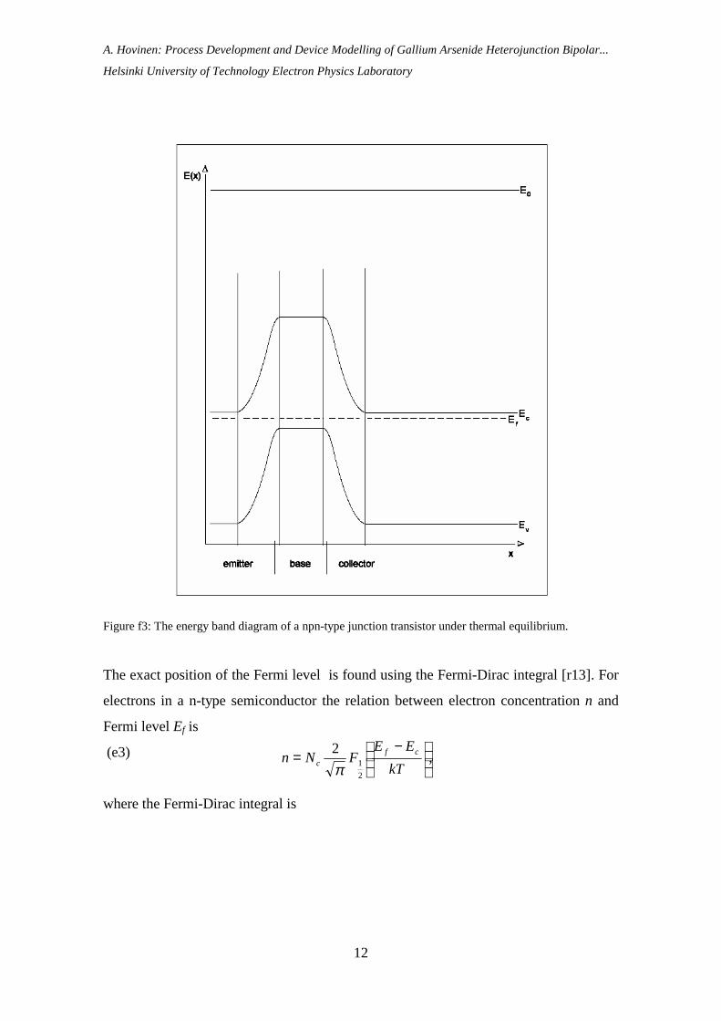
The energy band diagram of a npn-type junction transistor under thermal equilibrium is
presented in Figure f3. The energy level for vacuum E0 is included for convenience.
Vacuum energy level is always a straight line, as there is never spatial energy derivatives
associated with the vacuum level. If there was, one could emit electrons to the vacuum
level and absorp them back after a distance thus creating energy from nothing. The
dashed line inside the forbidden band gap is the “Fermi level” of energy Ef. The fermi
level concept comes from statistical physics and governs the flow of particles, such as
electrons and holes, in a same pictorial manner as temperature governs the flow of
energy. The electrons wish to move from the areas of higher Fermi level to the areas
where the Fermi level is lower. The energy separation between vacuum level E0 and

A. Hovinen: Process Development and Device Modelling of Gallium Arsenide Heterojunction Bipolar...
Helsinki University of Technology Electron Physics Laboratory
11
Fermi level Ef is the work function of the semiconductor material, or the amount of
energy in average that has to be supplied to the electron to remove it from the
semiconductor. Under thermal equilibrium, the Fermi level is constant throughout the
crystal.
The Fermi level energy and charge carrier concentrations are thus interdependent. The
Fermi level resides near conduction band edge on emitter and collector layers of the
npn-transistor because there the semiconductor crystal was doped n-type. On the p-type
base the Fermi level resides near the valence band edge. Figure f3 reveals that under
thermal equilibrium the energy band edges have to bend to keep the Fermi level
constant. The bending represents electric fields inside the crystal that have depleted free
electrons and holes from the region of bending. The aforementioned depletion region
edges are the points where the band derivative returns to zero. The regions with no
electrical field are the “neutral regions” of the semiconductor.
A. Hovinen: Process Development and Device Modelling of Gallium Arsenide Heterojunction Bipolar...
Helsinki University of Technology Electron Physics Laboratory
12
,2
2
1
−=
kT
EEFNn cf
c π
Figure f3: The energy band diagram of a npn-type junction transistor under thermal equilibrium.
The exact position of the Fermi level is found using the Fermi-Dirac integral [r13]. For
electrons in a n-type semiconductor the relation between electron concentration n and
Fermi level Ef is
(e3)
where the Fermi-Dirac integral is

A. Hovinen: Process Development and Device Modelling of Gallium Arsenide Heterojunction Bipolar...
Helsinki University of Technology Electron Physics Laboratory
13
,2
22
3
2 cde
c Mh
kTmN
=
π
,2
2
1
−=
kT
EEFNp fv
v π
,2
22
3
2
=
h
kTmN dh
v
π
,ln
432
⋅+
⋅+
⋅+
⋅+
=
−
ccccc
cf
N
nD
N
nC
N
nB
N
nA
N
n
kT
EE
( ) ( )∫∞
−+=
02
1 ,1
ηη
η ηη de
Ff
f
and Nc is the effective density of states in the conduction band, or
(e4)
where mde is the “density of states” effective mass for electrons, h is the Planck´s
constant, and Mc is the number of equivalent minima in the conduction band. For holes
in p-type material the relation is
(e5)
where Nv is the effective density of states in the valence band, or
(e6)
where mdh is the “density of states” effective mass for holes.
The Fermi-Dirac integral is mathematically involved. In practical calculations of this
thesis the relation between electron concentration n and Fermi level in n-type
semiconductor is obtained from the Joyce-Dixon approximation [r14],
(e7)
where A = 0,353553, B = -4,95009.10-3, C = 1,48386.10-4, and D = -4,42563.10-6. For
A. Hovinen: Process Development and Device Modelling of Gallium Arsenide Heterojunction Bipolar...
Helsinki University of Technology Electron Physics Laboratory
14
,ln
432
⋅+
⋅+
⋅+
⋅+
=
−
vvvvv
fv
N
pD
N
pC
N
pB
N
pA
N
p
kT
EE
.kT
EE
c
cf
eNn−
=
.kT
EE
v
fv
eNp−
=
hole concentration p in p-type semiconductor the Joyce-Dixon approximation is
(e8)
where the coefficients A, B, C and D are the same as previously. When the doping level
of the semiconductor is moderate, the Fermi Dirac integral can be approximated further.
The Boltzmann formula for n-type semiconductor is
(e9)
For p-type semiconductors the formula is
(e10)
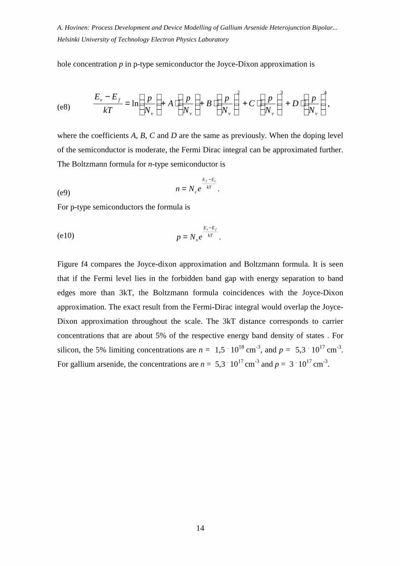
Figure f4 compares the Joyce-dixon approximation and Boltzmann formula. It is seen
that if the Fermi level lies in the forbidden band gap with energy separation to band
edges more than 3kT, the Boltzmann formula coincidences with the Joyce-Dixon
approximation. The exact result from the Fermi-Dirac integral would overlap the Joyce-
Dixon approximation throughout the scale. The 3kT distance corresponds to carrier
concentrations that are about 5% of the respective energy band density of states . For
silicon, the 5% limiting concentrations are n = 1,5 . 1018 cm-3, and p = 5,3 . 1017 cm-3.
For gallium arsenide, the concentrations are n = 5,3 . 1017 cm-3 and p = 3 . 1017 cm-3.

A. Hovinen: Process Development and Device Modelling of Gallium Arsenide Heterojunction Bipolar...
Helsinki University of Technology Electron Physics Laboratory
15
,2kT
E
vci
g
eNNn−
=
Figure f4: Comparison of Boltzmann approximation (dashed line) and Joyce-Dixon approximation (solid
line) of the Fermi-Dirac integral. The exact value of the integral would almost overlap the solid line as
verified in, e.g., [r14], page 34.
From equations (e1) , (e9), and (e10) the intrinsic carrier concentration ni can be
obtained,
(e11)
where Eg = (Ec - Ev ) is the width of the forbidden band gap. Because the calculation
included Maxwell-Boltzmann statistics, the formula for ni needs not to be valid with
heavily doped samples. It is seen from the formula that the intrinsic carrier concentration
of a semiconductor decreases exponentially as Eg increases. In practice, this has
application in the case of heterointerfaces, where semiconductive layers of different
band gaps are joined together in a manner that the crystal periodicity is maintained. The
electrical properties of the material change in a very short distance around the interface
allowing the design of modern semiconductor devices such as High Electron Mobility
Transistors (HEMTs) and Heterojunction Bipolar Transistors (HBTs).

A. Hovinen: Process Development and Device Modelling of Gallium Arsenide Heterojunction Bipolar...
Helsinki University of Technology Electron Physics Laboratory
16
2.2 Band Gap Tailoring
Figure f3 represented the energy band diagram of a conventional bipolar junction
transistor in thermal equilibrium. The forbidden band gap was of constant width
throughout the device. With modern processing methods, such as Molecular Beam
Epitaxy (MBE) or Metallo-Organic Chemical Vapour Deposition (MOCVD) it is
possible to make semiconductor crystals that include spatial modulation in the forbidden
band gap width. In epitaxial processing, the monocrystalline semiconductor material is
grown by stacking semiconductor atoms with almost molecular accuracy. The electrical
properties of the semiconductor are controlled by adding a specific amount of dopant
atoms and even varying the atoms that constitute the main crystal.
The heterojunction bipolar transistor gets its name from the composition of the
transistor structure. In a single heterojunction structure the emitter layer of the transistor
is made of material that has wider forbidden bad gap than base or collector layers. The
possible material choices are dictated by proper crystal lattice match between the layers.
Ideally, lattice constants between adjacent layers should be identical, thus no strain is
generated during epitaxial growth of the structure. Excess strain would break the bonds
between lattice atoms in the vicinity of heterojunction, yielding to imperfect crystal and
poor functionality of the transistor.
Figure f5 shows the lattice constant mapping of different semiconductor materials. As
can be seen, AlAs and GaAs have almost the same lattice constant, so any composition
of single crystal AlxGa1-x As is possible to be grown on top of GaAs crystal. The band
gap of the ternary compound adjusts with the AlAs mole fraction x. InGaP lattice
matched to GaAs is also possible. Other choices could be, e.g., GaAsSb lattice matched
to InP or GaInAs lattice mathed to InP. The traditional choice for a heterostructure
material pair has been AlxGa1-x As on top of GaAs, where AlAs mole fraction is kept
below 0,3 to avoid complications that arise from the AlxGa1-x As energy band diagram
shifting from direct band gap structure to indirect gap structure when x approaches 0,45
[r13].

A. Hovinen: Process Development and Device Modelling of Gallium Arsenide Heterojunction Bipolar...
Helsinki University of Technology Electron Physics Laboratory
17
GaAs/AlxGa1-xAs structure is the most studied material in high speed compound
semiconductor research, and its applications have matured to commercial level. In
recent years the compound semiconductor research has been bending towards studies on
GaN-AlN combination. It is seen in Figure f5 that the lattice match is good, and both the
energy gaps and their relative difference is appreciable. Nitrogen based compounds will
probably find their use in high temperature and high power applications in the future.
Figure f5: The lattice constant mapping of different III-V semiconductor materials. Silicon and
germanium values are also shown (red dots). Numerical data is collected from [r13] and [r15].
Band Gap Energies and Lattice Constants of Selected III-V Semiconductors
4
4.5
5
5.5
6
6.5
7
0 1 2 3 4 5 6 7
Band Gap Energy [eV]
Lat
tice
Co
nst
ant
[Å]
Al compounds
Ga compounds
In compounds
N compounds
P compounds
Sb compounds
As compounds
GaAs
Si
Ge
InSb
InAs
GaSb AlSb
AlAs
GaP
AlP
AlNGaN
InN
InP

A. Hovinen: Process Development and Device Modelling of Gallium Arsenide Heterojunction Bipolar...
Helsinki University of Technology Electron Physics Laboratory
18
.,, basegemittergg EEE −=∆
Figure f6: Energy band diagram of an abrupt heterojunction bipolar transistor. Numerical parameter
values that were used in the enegy band simulation are introduced in chapter 3.2.
The energy band diagram of a typical heterojunction bipolar transistor in thermal
equilibrium is shown in Figure f6. The device is npn-type with Al0,25Ga0,75As emitter,
GaAs base and GaAs collector. There are some differences to the conventional bipolar
transistor picture of Figure f3. Forbidden energy band gap width changes abruptly in the
base-emitter junction, as the emitter band gap is wider than in base or collector. This
generates the spike on the conduction band that is seen in the Figure f6. The difference
in band gap widths ∆Eg is
(e12)
The AlxGa1-xAs/GaAs heterojunction shares the bandgap difference ∆Eg between
conduction band difference ∆Ec and valence band difference ∆Ev so that
Energy Band Diagram for the Structure with Abrupt Heterojuntionin Thermal Equilibrium
-2
-1.5
-1
-0.5
0
0.5
1
1.5
2
0 1000 2000 3000 4000 5000 6000 7000 8000 9000
Distance from Surface [Å]
Energy [eV]
Conduction Band Edge
Valence Band Edge
Fermi Level

A. Hovinen: Process Development and Device Modelling of Gallium Arsenide Heterojunction Bipolar...
Helsinki University of Technology Electron Physics Laboratory
19
( ) ( )( )
≤<++
≤≤−=∆
1,0x0,45 ,143,00,55-0,1250,476
0,45x0 ,55,0247,12xx
xxEc
( )
( ) ( ) ( )xExExE
xxE
vcg
v
∆+∆=∆
≤≤=∆ 1x0 ,55,0
(e13)
where x is the AlAs mole fraction of the emitter and the energy unit is eV [r14]. The
equation for conduction band spike is deliberately presented in a form that emphasizes
its dependence on x with reference to valence band. Numerical values of band gap
discontinuities for practical calculations of this thesis rely on equations (e13).
2.3 Electrode Currents of a transistor
The main purpose of a transistor is to serve as a controllable conduit of charge carriers
from its emitter electrode to its collector electrode. The overall picture inside the conduit
includes also leaks and obstacles of various kind. One of the most important
relationships inside a transistor is how efficiently the base controls over the collector
current. Figure f6 gives a collection of relevant definitions and parameters for the
calculation of the electrode currents of a heterojunction bipolar transistor. The figure
represents a transistor in forward active mode as emitter-base junction is forward biased
and base-collector junction is reverse biased.
Figure f6: A collection of relevant definitions and parameters for the calculation of the electrode currents
of a heterojunction bipolar transistor.
A. Hovinen: Process Development and Device Modelling of Gallium Arsenide Heterojunction Bipolar...
Helsinki University of Technology Electron Physics Laboratory
20
perenee JJJJ ++=
.rgCrepeb JJJJJ +−+=
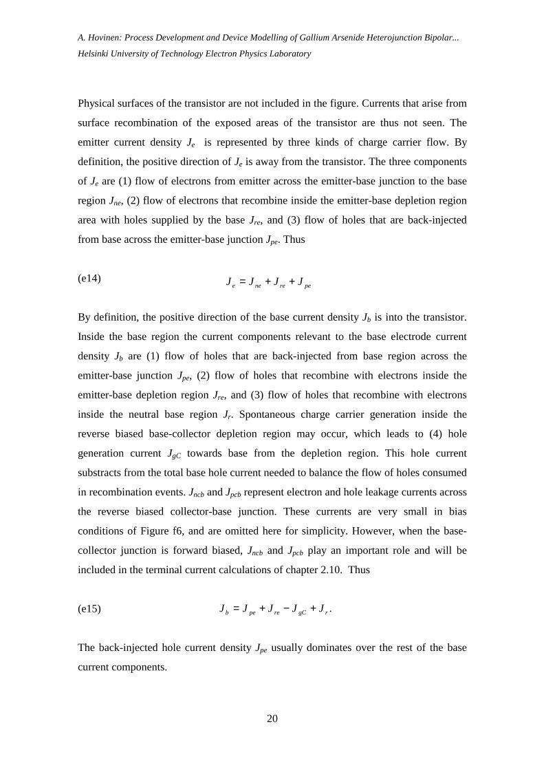
Physical surfaces of the transistor are not included in the figure. Currents that arise from
surface recombination of the exposed areas of the transistor are thus not seen. The
emitter current density Je is represented by three kinds of charge carrier flow. By
definition, the positive direction of Je is away from the transistor. The three components
of Je are (1) flow of electrons from emitter across the emitter-base junction to the base
region Jne, (2) flow of electrons that recombine inside the emitter-base depletion region
area with holes supplied by the base Jre, and (3) flow of holes that are back-injected
from base across the emitter-base junction Jpe. Thus
(e14)
By definition, the positive direction of the base current density Jb is into the transistor.
Inside the base region the current components relevant to the base electrode current
density Jb are (1) flow of holes that are back-injected from base region across the
emitter-base junction Jpe, (2) flow of holes that recombine with electrons inside the
emitter-base depletion region Jre, and (3) flow of holes that recombine with electrons
inside the neutral base region Jr. Spontaneous charge carrier generation inside the
reverse biased base-collector depletion region may occur, which leads to (4) hole
generation current JgC towards base from the depletion region. This hole current
substracts from the total base hole current needed to balance the flow of holes consumed
in recombination events. Jncb and Jpcb represent electron and hole leakage currents across
the reverse biased collector-base junction. These currents are very small in bias
conditions of Figure f6, and are omitted here for simplicity. However, when the base-
collector junction is forward biased, Jncb and Jpcb play an important role and will be
included in the terminal current calculations of chapter 2.10. Thus
(e15)
The back-injected hole current density Jpe usually dominates over the rest of the base
current components.

A. Hovinen: Process Development and Device Modelling of Gallium Arsenide Heterojunction Bipolar...
Helsinki University of Technology Electron Physics Laboratory
21
.gCrnEc JJJJ +−=
.gCpe
gCne
gCrrepe
gCrne
B
C
JJ
JJ
JJJJ
JJJ
I
I
−+
<−++
+−==β
By definition, the direction of the collector current density Jc is towards the transistor.
Inside the transistor the current components for Jc are (1) flow of electrons that originate
from emitter and have survived the travel without recombination, and (2) flow of
electrons that have been spontaneously generated inside the reverse biased base-
collector region. Thus
(e16)
The large signal current gain β of a transistor is defined as the ratio of the collector
current IC and base current IB [29]. With equal areas of emitter, base and collector
(e17)
This is the large signal current gain of the transistor. Small signal current gain is
obtained by dividing the differential increase of Ic with respective differential increase in
Ib. JgC is a weak function of base-collector voltage, and may be neglected in the
calculation. It is seen from the formula that the gain is maximized when the back
injected hole current across emitter-base junction is minimized.
2.4 Abrupt Heterojunction under thermal equilibrium
The equations governing electrical behaviour of the emitter-base heterojunction are
crucial in calculations of the analytical equations for transistor electrode currents. To
have the convenience of associating numerical values for the relevant parameters for
illustrative purposes, the case of an abrupt heterojunction of n-type Al0,3Ga0,7As and p-
type GaAs is chosen here. The energy band diagram of the structure in thermal
equilibrium is given in Figure f7. The depletion region with its immobile space charge
that originates from the ionized dopant atoms is also included, as is the respective
electrical field. X1 is the depletion region edge in base side, and X2 is the emitter side
depletion region edge. Xje represents the metallurgical junction. The rest of the variables
are defined as they occur in the analysis of the structure.
To verify that the picture may be correct, a hypothetical experiment can be carried out.

A. Hovinen: Process Development and Device Modelling of Gallium Arsenide Heterojunction Bipolar...
Helsinki University of Technology Electron Physics Laboratory
22
In a infinite bar of intrinsic GaAs in thermal equilibrium at temperature of 300K the
Fermi level resides approximately in the middle of the forbidden band gap. Carrier
concentrations n and p equal the intrinsic carrier concentration ni or 2,6.106 cm-3
throughout the bar. Then, half of the bar is changed for intrinsic Al0,3Ga0,7As without
breaking the crystal periodicity on the junction. On the junction, the conduction band
and valence band would be discontinuous, with an amount given in equation (e13). Far
apart from junction the Fermi level still resides around the middle of the band gap. For
Al0,3Ga0,7As the intrinsic carrier concentration is about 1,7.103 cm-3. Initially, the free
electrons in AlGaAs-side of the junction see the lower Fermi level of GaAs and jump
over the junction. The electron leaves a positively charged immobile crystal ion behind,
and after recombining with a hole in the GaAs side another, negatively charged
immobile ion is formed. The immobile ions constitute an electrical dipole with electric
field that points from AlGaAs towards GaAs.
Figure f7: The energy band diagram of an abrupt heterojunction of n-type Al0,3Ga0,7As and p-type GaAs in
thermal equilibrium.
A. Hovinen: Process Development and Device Modelling of Gallium Arsenide Heterojunction Bipolar...
Helsinki University of Technology Electron Physics Laboratory
23
),( −+ −+−= NNnpq
dx
dF
sε
( ) ).(xFxD sε=
.)()2(2
1∫
−
−=X
X
dxxFXV
The direction of the field is such that it repels electrons from further movement across
the junction. The movement of electrons continue until the cumulative repulsive force
of the space charge region is strong enough to maintain an equilibrium. When the
equilibrium is reached, Fermi level would be constant all over the bar.
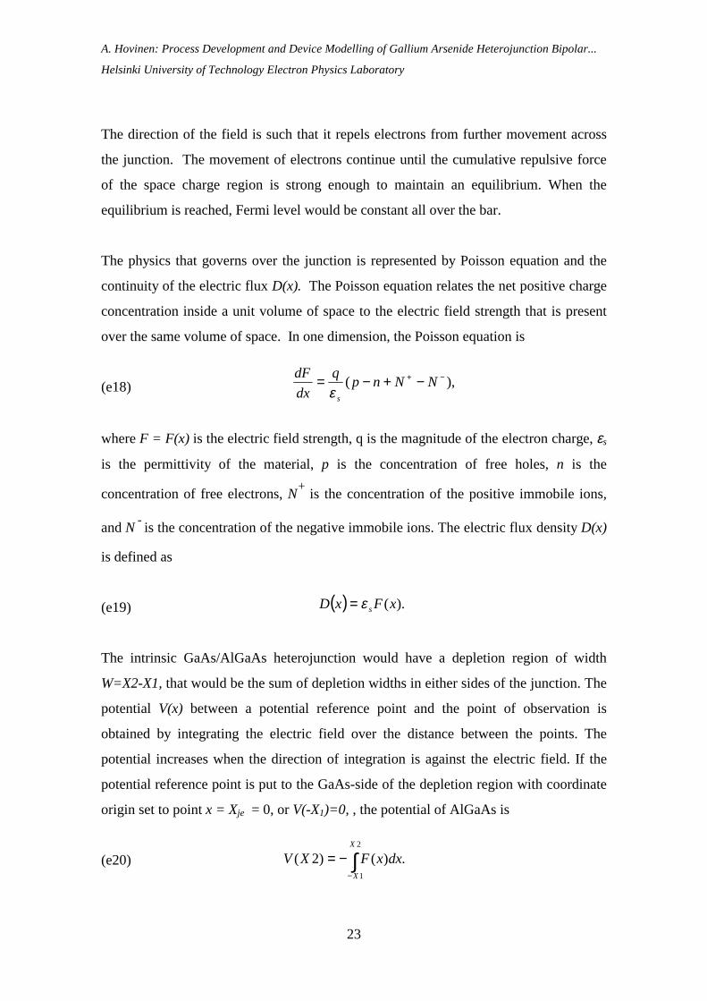
The physics that governs over the junction is represented by Poisson equation and the
continuity of the electric flux D(x). The Poisson equation relates the net positive charge
concentration inside a unit volume of space to the electric field strength that is present
over the same volume of space. In one dimension, the Poisson equation is
(e18)
where F = F(x) is the electric field strength, q is the magnitude of the electron charge, εs
is the permittivity of the material, p is the concentration of free holes, n is the
concentration of free electrons, N+ is the concentration of the positive immobile ions,
and N - is the concentration of the negative immobile ions. The electric flux density D(x)
is defined as
(e19)
The intrinsic GaAs/AlGaAs heterojunction would have a depletion region of width
W=X2-X1, that would be the sum of depletion widths in either sides of the junction. The
potential V(x) between a potential reference point and the point of observation is
obtained by integrating the electric field over the distance between the points. The
potential increases when the direction of integration is against the electric field. If the
potential reference point is put to the GaAs-side of the depletion region with coordinate
origin set to point x = Xje = 0, or V(-X1)=0, , the potential of AlGaAs is
(e20)
A. Hovinen: Process Development and Device Modelling of Gallium Arsenide Heterojunction Bipolar...
Helsinki University of Technology Electron Physics Laboratory
24
,21
)2( 121 q
EEVVXVV cg
bbbi
Θ−Θ−∆+=+==
. X2]x[0
0]x[-X1
22
11
<<=
<<−=
is
is
nq
dx
dF
nq
dx
dF
ε
ε
( ).)1)(1
11
11
∫−
+−=
−=
x
X
is
is
Xxnq
dxnq
xFεε
,)0()0()(0
22
22
∫ +=
+= ++
x
is
is
xnq
Fdxnq
FxFεε
).0()0()0()0( 21++−− === FDFD ss εε
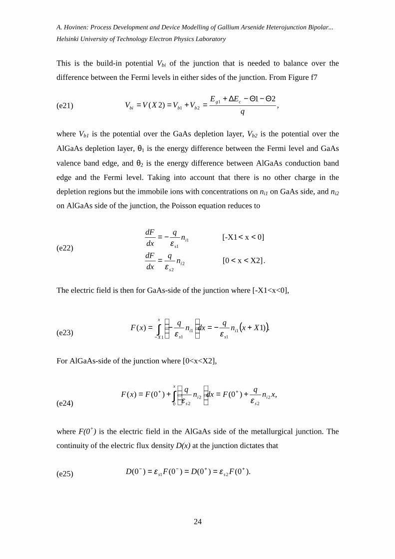
This is the build-in potential Vbi of the junction that is needed to balance over the
difference between the Fermi levels in either sides of the junction. From Figure f7
(e21)
where Vb1 is the potential over the GaAs depletion layer, Vb2 is the potential over the
AlGaAs depletion layer, θ1 is the energy difference between the Fermi level and GaAs
valence band edge, and θ2 is the energy difference between AlGaAs conduction band
edge and the Fermi level. Taking into account that there is no other charge in the
depletion regions but the immobile ions with concentrations on ni1 on GaAs side, and ni2
on AlGaAs side of the junction, the Poisson equation reduces to
(e22)
The electric field is then for GaAs-side of the junction where [-X1<x<0],
(e23)
For AlGaAs-side of the junction where [0<x<X2],
(e24)
where F(0+) is the electric field in the AlGaAs side of the metallurgical junction. The
continuity of the electric flux density D(x) at the junction dictates that
(e25)

A. Hovinen: Process Development and Device Modelling of Gallium Arsenide Heterojunction Bipolar...
Helsinki University of Technology Electron Physics Laboratory
25
( ) ,10 12
Xnq
F isε
−=+
( ) ( ).1 212
xnXnq
xF iis
−−=ε
,21 21 XnXn ii =
( ) ( ) ( ) .12
.1 21
11
11
Xxnq
Xxnq
xV is
x
X
is
+=
+−−= ∫
− εε
( ) .12
0 21
11 Xn
qxVV i
sb ε
=== −
( ) ( ).22
2 xXqn
xFs
i −−=ε
( ) ( ) .2
222
2
21
0 2
21
−+=
−−−= ∫
xxX
qnVdxxX
qnVxV
s
ib
x
s
ib εε
Substituting F(0+) from equation (e23) it is found that
(e26)
which after substitution into equation (e24) gives for [0<x<X2]
(e27)
At the depletion region edge X2 the electric field F(X2) is zero. This underscores the
charge conservation relationship over the depletion region,
(e28)
and gives for [0<x<X2]
(e29)
The potential V(x) can now be calculated by integrating the electric field over the
depletion layer. For GaAs side [-X1<x<0] with the boundary condition that V(-X1)=0,
(e30)
The potential over GaAs side depletion region obeys parabolic curvature. The potential
at the junction is
(e31)
Similarly, after taking into account that potential is continuous at the junction, potential
over AlGaAs [0<x<X2] is
(e32)

A. Hovinen: Process Development and Device Modelling of Gallium Arsenide Heterojunction Bipolar...
Helsinki University of Technology Electron Physics Laboratory
26
( ) .22
12
2 22
2
21
121 Xn
qXn
qVVXxVV i
si
sbbbi εε
+=+===
22
112
12
221
1
2
1
2
si
si
is
is
b
b
n
n
Xn
Xn
V
V
εε
εε
==
.11 122
111
1
2b
si
sib
b
bbi V
n
nV
V
VV
+=
+=
εε
( ) ( ) ,083.0067.0 0mxxmde +=
The build-in potential over the depletion region is thus
(e33)
The unknown depletion region widths X1 and X2 can be solved by taking the ratio of
Vb1 and Vb2 and substituting the charge conservation equation (e28) to get
(e34)
which is then substituted to the equation (e33) of Vbi,
(e35)
Equation (e21) relates the build-in potential to the Fermi levels θ1 and θ2. Equations
(e9) and (e10) relate the Fermi levels to free electron and hole concentrations. For θ1 =
Ef - Ev in GaAs neutral region the numerical values of p = ni1 = 2,6.106cm-3 and Nv =
7.1018cm-3 give from equation (e10) θ1=0,74 eV. For θ2=Ec-Ef in AlGaAs neutral region
the numerical value of n equals ni2 = 1,7.103cm-3. To determine a numerical value of
effective density of states Nc for AlxGa1-xAs conduction band, the effective electron
mass mde has to be known in equation (e4). For material with AlAs mole fraction x
below 0,45, the effective electron mass mde = mde(x) is [r14]
(e36)
where m0 is the free electron mass. For Al0,3Ga0,7As the numerical value of Nc from
equation (e4) is then Nc = 7.1017cm-3. From equation (e9), Fermi level position in the
neutral region of AlGaAs is θ2 = 0,87 eV. The conduction band discontinuity ∆Ec for
equation (e21) is found from equation (e13), and is ∆Ec = 0,2091 eV. The forbidden
energy bang gap width of GaAs in room temperature is Eg1 = 1,424 eV, and the AlGaAs
forbidden energy bang gap width from equation (e13) is then Eg2 = 1,798 eV.
Substituting the numerical values to equation (e21) the build in potential Vbi of an
intrinsic Al0,3Ga0,7As/GaAs heterostructure is 23,82 mV. To get Vb1 from equation (e35)

A. Hovinen: Process Development and Device Modelling of Gallium Arsenide Heterojunction Bipolar...
Helsinki University of Technology Electron Physics Laboratory
27
( ) 1,0x0 ,12,318,13 02 ≤≤⋅−= εε xs
the permittivities εs1 and εs2 need to be known. For GaAs, εs1 is 13,18. ε0, where ε0 is
the permittivity of vacuum. For AlxGa1-xAs the permittivity varies approximately
linearly with x [r14],
(e37)
which for x=0,3 gives εs2 = 12,24. ε0. Equation (e35) gives then Vb1 = 14,46µV.
Practically all of the build-in potential is over the AlGaAs depletion layer. The depletion
region widths as obtained from equation (e33) are X1 = 90 µm and X2 = 0,137 meters. It
is seen from equation (e28) that X1 and X2 conserve the total charge across the depletion
region of the junction.
The hypothetical GaAs/AlGaAs bar is now ready to be doped with impurities in order to
create a pn-heterojunction. Dopant atoms are thus being supplied uniformly into the two
bar halves in a way that GaAs gets carbon atoms that are p-type dopants or acceptors,
and AlGaAs gets silicon atoms that are n-type dopants or donors. The doping atoms are
such that in normal operation temperatures practically all of the dopant atoms are
ionized so that added hole concentration p will be approximately equal to carbon doping
concentration NA, and added electron concentration n will be approximately equal to
silicon doping concentration ND.
Excess electrons are thus introduced in AlGaAs and excess holes into GaAs. In AlGaAs
side the Fermi level starts to drift upwards in energy, and in GaAs side downwards in
energy. In the vicinity of the junction the excess electrons in AlGaAs see again the
lower Fermi level on GaAs side and wish to fill the holes in GaAs side. In every
movement of electron, a positive and immobile space charge is formed in the AlGaAs
side and negative and immobile space charge is formed in the GaAs side. The space
charges continue forming electrical dipoles that cumulative strengthen the electric field
across the junction.

A. Hovinen: Process Development and Device Modelling of Gallium Arsenide Heterojunction Bipolar...
Helsinki University of Technology Electron Physics Laboratory
28
As the typical doping levels are several orders of magnitude higher than intrinsic
concentrations, the intentional doping soon dominates the electrical behaviour of the
material at room temperature. The field direction is still from AlGaAs towards GaAs
representing a repulsive force against further movement of electrons. Depending on the
doping levels, more or less electrons move across the junction until equilibrium is again
formed by the repulsive electric field of the space charge dipole. At equilibrium, the
Fermi level is again constant throughout the structure. The calculations that were done
for an intrinsic heterosructure can now be repeated, taking into account that the
immobile space charge now consitutes almost entirely by the ionized dopant atoms. If
the doping consentrations exceed the validity limit of the Boltzmann equation (e9) and
(e10), the Joyce-Dixon approximation of equation (e7) and (e8) should be used.
With doping concentrations of NA = 1.1019cm-3 and ND = 1.1017cm-3 the Fermi level
positions accroding to equations (e7) and (e8) are Θ2 = +48,948 meV and Θ1 = -22,019
meV. The negative Fermi level position indicates that Fermi level is now below valence
band edge in p-doped GaAs. From equation (e21) the built-in potential is found to be
Vbi = 1,606 V. Potential across GaAs side of the junction is from equation (e35) Vb1 =
14,78 mV, and the GaAs-side depletion region width from equation (e31) is X1 = 14,67
Å. For AlGaAs, the calculation gives Vb2 = 1,59136 V, and X2 = 14,67 µm. Again, the
total charge is conserved. The huge difference in doping levels make the junction
practically one sided. Schematically, the energy band diagram looks like that of Figure
f7, although the narrow depletion region in GaAs side would not be visible.

A. Hovinen: Process Development and Device Modelling of Gallium Arsenide Heterojunction Bipolar...
Helsinki University of Technology Electron Physics Laboratory
29
,21 jjAbij VVVVV +=−=
2.5 AlGaAs / GaAs –Heterojunction Under Applied Voltage
The heterojunction of Figure f7 forms a diode structure. If external voltage VA is applied
such that GaAs is forced more positive than AlGaAs, the thermal equilibrium is
disturbed as illustrated in Figure f8. The applied potential difference is seen by the
junction as a shift between Fermi levels in each side of the depletion region. In AlGaAs-
side the level shifts upwards in energy, and in GaAs-side downwards.
Figure f8: Heterojunction under applied voltage.
The overall potential Vj across the junction is now
(e38)
where Vj1 is the potential over GaAs-side depletion layer, and Vj2 is the potential over
AlGaAs-side depletion layer. Again, the electrons in AlGaAs wish to jump over the

A. Hovinen: Process Development and Device Modelling of Gallium Arsenide Heterojunction Bipolar...
Helsinki University of Technology Electron Physics Laboratory
30
,21
21
222
111
bbbi
AAA
Abj
Abj
VVV
VVV
VVV
VVV
+=+=
−=
−=
.1 122
11j
si
siAbij V
n
nVVV
+=−=
εε
( ) ( ) .2
2
2
1
2
22
1
21
221121s
s
s
sAbAbjjj
XqnXqnVVVVVVV
εε+=−+−=+=
junction to reach the lower Fermi level region. For every electron that leaves AlGaAs,
an electron is supplied by the negative terminal of the voltage supply that is connected
to the AlGaAs side of the diode. In GaAs side, the electron recombines with a hole,
which is then replaced by another hole that is generated by an electron leaving the bar to
the positive terminal of the voltage supply, that is connected to the GaAs side of the
diode. Electrical current flows through the diode indicating that the diode is forward
biased. If the polarity of the voltage supply is reversed, the Fermi level in AlGaAs shifts
downwards, and upwards in GaAs. The potential Vj would increase by an amount of
VA.
The applied potential VA is shared between the junction sides such that
(e39)
where VA1 is the portion of applied voltage VA over GaAs-side depletion region and VA2
is the portion of applied voltage over AlGaAs-side depletion region. Vbi = Vb1 + Vb2 is
the build-in potential of the junction under thermal equilibrium. Equation (e35) can now
be rewritten in applied bias condition
(e40)
Equation (e33) under applied bias is
(e41)
It is seen from equation (e41) that when forward applied voltage equals Vbi the depletion
region width goes zero. At that point, the energy band diagram of the junction is flat as
there is no space charge present. Band edges and the Fermi level then alter stepwise at
the metallurgical junction.

A. Hovinen: Process Development and Device Modelling of Gallium Arsenide Heterojunction Bipolar...
Helsinki University of Technology Electron Physics Laboratory
31
.densitycurrent hole emitteddensitycurrent electron emitted
densitycurrent electron emitted
+=γ
2.6 Current through abrupt AlGaAs / GaAs –Heterojunction
The discontinuities of energy bands in an abrupt AlGaAs/GaAs -heterojunction serve as
potential barriers against charge carrier movement across the junction. The discontinuity
of valence band ∆Ev impedes hole injection from GaAs to AlGaAs. The conduction
band spike ∆Ec impedes electron injection from AlGaAs to GaAs. From equation (e17)
it was seen that transistor current gain β depends on the ratio of injected electrons and
back-injected holes. It is customary to characterize the transistor emitter function by
“emitter efficiency” γ,
(e42)
The valence band discontinuity improves emitter efficiency by reducing back-injection
of holes. The conduction band discontinuity is more problematic. While the spike
reduces electron current and emitter efficiency it filters the electrons in energy such that
there is a considerable portion of high energy electrons included in the electron flow
[r48]. The high energy electrons are those that have enough energy to surmount the
spike from AlGaAs to GaAs. The excess energy is kinetic, and the base transit time is
smaller than with electrons at the edge of the conduction band. The transistor can thus
operate faster. For applications where high energy electron emission is not important,
the AlGaAs/GaAs junction is spatially graded, such that the AlAs mole fraction x is
altered gradually over a distance instead of having an abrupt profile. In a properly
graded junction the conduction band spike is absent, and the structure resembles a
homojunction with the exception of having different band gaps.
The generation of high energy electrons in an abrupt heterojunction is an example of
“thermionic emission”. It is the solid state counterpart of the electron tube triode emitter
function. Additionally, quantum mechanics gives the electrons behind the spike yet
another way to reach the GaAs side. The potential spike is thin enough to allow the
electron to have a finite probability to tunnel through the potential barrier. With

A. Hovinen: Process Development and Device Modelling of Gallium Arsenide Heterojunction Bipolar...
Helsinki University of Technology Electron Physics Laboratory
32
,2*sm
kT
qV
kT
q AB
eeTAJφ−
=
.4
3
2**
h
kqmA eπ
=
,22* Θ+= bB qVφ
approximately triangular shape of the spike there is always tunneling present to some
extent. The flow of electrons that tunnel through the spike constitute “field emission”
current across the junction. The emission modes are illustrated in Figure f9. Also
included in the figure are recombination currents that arise from recombination in the
depletion region and in the neutral region of AlGaAs. The total emitter current is a sum
of recombination currents and the combination of thermionic and field emission
currents.
Figure f9 has some similarity to the ideal metal-semiconductor Schottky-junction of
Figure f11. If the p-side was heavily doped almost all of the junction voltage is across
the AlGaAs depletion region. This allows to estimate the heterojunction thermionic
emission current with an analogy to the analysis of a Schottky junction. The Schottky
barrier height φB is defined as the separation of the metal Fermi level and the edge of the
conduction band spike. The current density from the flow of electrons from
semiconductor to metal with the ideal Schottky junction Jsm is [r13]
(e43)
where φB is in electron volts, VA is the applied bias voltage and A* is the effective
Richardson constant
(e44)
Here me* is the “conductivity” effective electron mass. At zero bias Jsm has a value that
balances against the current flow from metal to semiconductor such that net current is
zero. With the heterojunction of Figure f9 the Schottky barrier height φB is replaced by
φB*, or the Fermi level separation from the edge of the conduction band spike in AlGaAs
side,
(e45)
where Vb2 is the portion of the built-in potential Vbi that is over AlGaAs-side depletion
layer and θ2 is the energy difference between AlGaAs conduction band edge and the
Fermi level.

A. Hovinen: Process Development and Device Modelling of Gallium Arsenide Heterojunction Bipolar...
Helsinki University of Technology Electron Physics Laboratory
33
Figure f9: Emission modes and recombination currents of a heterojunction barrier.
Figure f11: Ideal metal-semiconductor Schottky-junction.

A. Hovinen: Process Development and Device Modelling of Gallium Arsenide Heterojunction Bipolar...
Helsinki University of Technology Electron Physics Laboratory
34
,1
121*
K
KEE cgB +
Θ−Θ+∆+=φ
.1
2
As
Ds
N
NK
εε
=
.1
12 K
V
K
VV jj
j +==
.11
11
2**21
21
K
V
kT
qK
KEE
kTjcg
eeTAJ +−
+
Θ−Θ+∆+−
=
.111
11
2**emission thermionic
21
−= +
−
+
Θ−Θ+∆+−
K
V
kT
qK
KEE
kTjcg
eeTAJ
The potential over Schottky junction VA is replaced by the potential drop over AlGaAs
Vj2. Replacing intrinsic concentrations with intentional doping concentrations NA and ND
in equations (e34) and (e35), and using equation (e21) φB* would be
(e46)
where
(e47)
The equation for Vj2 from equation (e40), after replacing intrinsic concentrations with
intentional doping concentrations NA and ND, is then
(e48)
The equation for thermionic emission current density from the flow of electrons from
AlGaAs to GaAs with an abrupt heterojunction and heavy p-doping is then
(e49)
At zero bias the electron current J21* balances the current J12
* which flows from GaAs to
AlGaAs. The total current density across the junction would be the sum of the current
flows J21* and J12
* , or
(e50)

A. Hovinen: Process Development and Device Modelling of Gallium Arsenide Heterojunction Bipolar...
Helsinki University of Technology Electron Physics Laboratory
35
.122
12
−
+= kT
qV
An
n
Dp
pShockley
j
ii eN
n
L
qD
N
n
L
qDJ
It has to be kept in mind that the ideal Schottky junction current equation (e43) is
derived under the following assumptions [r13]:
1) Schottky barrier height is much larger than kT
2) Thermal equilibrium is established at the plane that determines emission
3) The existence of a net current flow does not affect this equilibrium, so that the
opposite current fluxes can be superimposed.
The collector current density JC of a transistor with graded heterojunction emitter is
limited by the electron diffusion through the neutral base. If the heterojunction was
abrupt, the picture includes high energy, high velocity electrons in base that have either
tunneled through the spike or had enough energy to surmount it completely. In this case
the collector current density is not entirely related to the diffusion properties in the base.
Only if the height of the conduction band spike was small enough such that the electrons
loose their excess kinetic energy completely far before they reach the collector, the
transistor collector current is again limited by the diffusion of electrons with energies at
the conduction band edge level.
2.7 Current through graded AlGaAs / GaAs –Heterojunction
In a graded heterojunction the electron flow across the depletion region is not affected
by a potential spike. The ideal current equation follows that of Shockley equation of a
pn-homojunction [r13]. After taking into account that the material type changes from
GaAs to AlGaAs at the junction altering the intrinsic carrier density ni and therefore
minority carrier concentrations at thermal equilibrium pn0 and np0, the Shockley equation
for a graded, long heterojunction diode structure reads
(e51)
Here ni1 is intrinsic carrier density in GaAs, ni2 is intrinsic carrier density in AlGaAs, Dp
is the hole diffusion coefficient in n-type AlGaAs, Dn is the electron diffusion
coefficient in p-type GaAs, Lp is the hole diffusion length in n-type AlGaAs, and Ln is
the electron diffusion length in p-type GaAs.

A. Hovinen: Process Development and Device Modelling of Gallium Arsenide Heterojunction Bipolar...
Helsinki University of Technology Electron Physics Laboratory
36
.,
2,
,np
npnp D
L=τ
( ) ( ) .112
22
12
−
−+
−= kT
qV
AB
n
DE
pShockley
j
ii eN
n
XX
qD
N
n
XX
qDJ
( ),
dx
xdnqDJ nn =
By definition, the diffusion coefficient and diffusion length is bound together by the
minority carrier lifetime τ,
(e52)
A long diode structure is such that the diode extends over three times the diffusion
length in either direction away from the metallurgical junction. If the diode is short, the
diffusion lengths in equation (e51) are replaced by the neutral region thicknesses of
either side. If XE is the thickness n-AlGaAs layer and XB is the thickness p-GaAs layer,
the equation for a graded, short heterojunction diode would be
(e53)
2.8 Transistor Base Layer as a Charge Storage
Estimates on transistor terminal currents can be calculated by treating the base neutral
region as a storage volume of minority carrier charge. The storage is being filled on
emitter side by electron emission, and dynamic equilibrium is maintained by electrons
escaping the storage to collector side. Some electron are lost from the storage by
recombination processes that adds to total base current. Across the storage a gradient in
minority carrier concentration has to be present such that there is more electrons in
emitter side than in collector side of the storage volume.
The gradient of minority carrier concentration of electrons n(x) induces diffusion of
electrons in p-type GaAs base. The current density Jn from diffusion of electrons is
(e54)
where q is the magnitude of electron charge and Dn is the electron diffusion coefficient
in p-type GaAs. Because the concentration gradient decreases towards collector, the
direction of the diffusion current density Jn is towards emitter. Under steady state

A. Hovinen: Process Development and Device Modelling of Gallium Arsenide Heterojunction Bipolar...
Helsinki University of Technology Electron Physics Laboratory
37
( ) ( ) ( ) ( ),)(
+−=+−=
dx
dxxdn
dx
xdnqDdxxJxJxdJ nnnn
.)(
)( 0
n
nxnxU
τ−
=
( )
( ).
)(
)(
2
20
dx
xndD
nxn
dx
xdJxqU
nn
n
=−
⇔
=
τ
condition the net electron concentration inside an infinitesimal volume element of width
dx is constant in time. If there was any recombination event inside the volume element,
not all of the incoming electrons reach the collector side. The portion of electron flow
that does not come out at collector side of the volume element is
(e55)
which equals the electron flow into recombination events.
The minority carrier recombination lifetime τ is defined as the average time that is
needed by a volume element with excess minority carriers to reach again the
equilibrium by recombination. The recombination rate U measures the average
recombination process in [cm-3s-1]. For electrons in p-type GaAs
(e56)
where n0 is the minority electron concentration in p-type GaAs at thermal equilibrium.
In steady state the current density from recombinations inside the volume element
balances the diffusion current loss giving
(e57)

A. Hovinen: Process Development and Device Modelling of Gallium Arsenide Heterojunction Bipolar...
Helsinki University of Technology Electron Physics Laboratory
38
.0)()(
22
2
=−nL
xn
dx
xnd
,)0(21
0kT
qV
A
ikT
qV
b
jeje
eN
nenn ==+
,)(21
0kT
qV
A
ikT
qV
bc
jcjc
eN
nenXn ==−
In order to solve n(x) boundary conditions have to be set. Let the neutral base layer be
limited by the emitter-base depletion region edge at x = 0+ and the base-collector
depletion region edge at x = Xc-. Assuming a graded heterojunction the pn-junction law
of equation (e2) should hold, and
(e58)
where Vje is the potential difference of the base and emitter neutral regions that
approximately equals base-emitter voltage VBE, and n0b is the minority electron
concentration in base at thermal equilibrium. On collector side the pn-junction law reads
(e59)
where Vjc is the potential difference of the base and collector neutral regions that
approximately equals base-collector voltage VBC.
With a heavily doped base the thermal equilibrium electron concentration n0b is very
low. With NA =1.1019cm–3 and ni1 = 2,6.106cm-3 n0b = 6,76.10-7cm–3. For a transistor
operating in forward active mode Vje > 0V and Vjc < 0V. With Vje = 1 V and Vjc = -1 V
n(0+) = 4,3.1010cm–3 and n(Xc-) = 1,1.10 -23 cm–3, which is practically zero.
A very simple formula for the the diffusion current density Jn across the base can be
derived if it is postulated that the minority electron concentration n(x) across the neutral
base layer of a transistor biased into forward active mode is always much more than the
thermal equilibrium value n0b. With equation (e52) equation (e57) would then reduce to
(e60)

A. Hovinen: Process Development and Device Modelling of Gallium Arsenide Heterojunction Bipolar...
Helsinki University of Technology Electron Physics Laboratory
39
( ) ( ),
0
−
−
=−
−−
−
+n
base
n
base
n
base
n
base
L
xW
L
xW
L
W
L
Wee
ee
nxn
( ) ( ) .10
−≈ +
baseW
xnxn
.)0()( 2
1,
kT
qV
A
i
base
n
basen
Xxndiffc
je
c
eN
n
W
qD
W
nqD
dx
xdnqDJ ===
+
= −
The solution for n(x) that satisfies boundary conditions of equation (e58) and n(Xc-)=0 is
(e61)
where Wbase = Xc-
- 0+ is the thickness of the neutral base region. With small values of z
the exponential function ez is approximately equal to 1+z. It is seen from equation (e61)
that the equation of n(x) when Wbase<<Ln reduces further to
(e62)
The electron concentration has a linear dependence on the distance from the emitter side
of the neutral base, and goes zero at the collector side of the neutral base. From (e54)
the current density from diffusion of electrons across the base is then constant over the
base. The collector current density from diffusion of electrons across the base Jc,diff
would then be
(e63)
The necessary condition for equation (e63) to hold is that Wbase<<Ln. Typical values for
recombination lifetime and diffusion coefficient of electrons in heavily doped p-GaAs
are τn ~ 1 ns and Dn ~25 cm2s-1, giving diffusion length Ln of about 1,5 µm. Typical
base thicknesses are around 0,1 µm or less, indicating that equation (e63) is applicable.
What was also assumed was that the heterojunction was graded, and the pn-junction law
gives the minority carrier concentration at the emitter side of the neutral region of base.
With abrupt heterojunctions the electron concentration is determined by the combination
of thermal and field emission. In that case the derivation of collector current equation is
somewhat more involved, giving for the total collector current JC [r14]

A. Hovinen: Process Development and Device Modelling of Gallium Arsenide Heterojunction Bipolar...
Helsinki University of Technology Electron Physics Laboratory
40
( ),1
0000 coth1
0
−=
−
+
kT
qV
kT
EEK
qV
C
je
je
eeJJ
.4 2
*00
se
D
m
NqhE
επ=
,, scdriftc vqnJ =
( ) ( )s
diffcccc qv
JnXnXn ,=== +−
(e64)
where J0 is a constant and
There was many approximations involved with equation (e61). In reality, the carrier
concentration at the collector depletion region edge is far from zero when the transistor
is biased to forward active mode. The current density through base-collector junction
should be continuous. After reaching the base-collector depletion region the electrons
are accelerated by the strong electric field of the reverse biased junction until they
achieve the saturation velocity vs. The corresponding current density from electrons
Jc,drift would be [r51]
(e65)
where nc is the mobile electron concentration inside the base-collector depletion region.
It was assumed with equation (e59) that under forward active mode the electron
concentration at the collector side of the neutral base drops to practically zero. To
maintain the current continuity, the approximation needs to be refined to give
(e66)
With a typical value of vs = 1.107 cm/s and current density of 1kA/cm2 nc ~ 6,2.1014 cm-3.
With neutral base thickness of 1000Å and Dn = 25 cm2s-1, this would demand from
equation (e63) that n(0+) = 2,5.1015 cm-3. With base doping of NA =1.1019cm–3 and ni1 =
2,6.106cm-3 the emitter-base bias potential should be Vje = 1,28 V.

A. Hovinen: Process Development and Device Modelling of Gallium Arsenide Heterojunction Bipolar...
Helsinki University of Technology Electron Physics Laboratory
41
.n
r
QJ
τ=
( ) ( )( ) .10 cbase
c nW
xnnxn +
−−≈ +
( ) ( )[ ].020
cbase
W
nnWq
dxxnqQbase
+== +∫
( ) .20
12
22
, n
basec
n
base
diffcb D
W
n
n
D
W
J
Q ≈
+== +τ
( ) ( )
.
.022
2
=∆−∆
nL
xn
dx
xnd
To correct the picture of minority carrier concentration profile across the charge storage
in order to maintain current continuity at x = Xc, equation (e62) may be rewritten as
(e67)
The total charge density Q of the base layer under forward active mode is obtained by
integrating n(x) over the neutral base and multiplying by electron charge q,
(e68)
The definition of recombination lifetime of equation (e56) and equation (e68) gives the
base current density from recombinations inside the neutral base Jr as
(e69)
The base transit time τb of a charge carrier population is the time needed to drain the
stored charge by the collector current,
(e70)
For accurate characterization of the transistor behaviour equation (e57) need to be
solved with more accurate boundary condition for x = Xc. It is common to rewrite the
continuity equation (e57) for the excess charge carrier concentration ∆n = n(x) - no,
where no is the thermal equilibrium electron concentration in the base layer. Equation
(e57) then reads
(e71)
A. Hovinen: Process Development and Device Modelling of Gallium Arsenide Heterojunction Bipolar...
Helsinki University of Technology Electron Physics Laboratory
42
( ) ,22
22
0
kT
qV
D
i
emitter
pkT
qV
D
i
E
pp
jeje
eN
n
W
qDe
N
n
XX
qDJ =
−= −
( ) ,
sinh
sinh)0(sinh)(
)(xn 0
−∆−
∆
=−=∆−
−+−
n
c
n
c
nc
L
X
L
Xxn
L
xXn
nxn
The solution for ∆n(x) that satisfies boundary conditions of equation (e58) and (e59) is
(e72)
where ∆n(0+) = n(0+)-n0 and ∆n(Xc- ) = n(Xc
-)-n0.
2.9 Large Signal Current Gain of a Heterojunction Bipolar Transistor
The current gain of a transistor was introduced with equation (e17) as the ratio of
collector and base currents. The gain was limited by the ratio of forward injected
electrons to back-injected holes in the forward biased base-emitter junction. With a
graded heterojunction emitter the flow of electrons and holes is limited by diffusion and
Shockley equation of (e53) holds. With abrupt heterojunction the flow of electrons is
not necessarily limited by diffusion because of the conduction band spike.
The flow of holes is not impeded by any spike but only a valence band difference of
∆EV. Hole current is limited by diffusion and Shockley equation is valid, such that the
back-injected hole current density in a short base-emitter diode in either type of
heterojunction is
(e73)
where XE is emitter contact, X0- is emitter side depletion region edge, Wemitter = XE –X0
-
is the thickness of the neutral emitter. Substituting (e73) and (e63) into (e17) gives for a
graded heterojunction transistor

A. Hovinen: Process Development and Device Modelling of Gallium Arsenide Heterojunction Bipolar...
Helsinki University of Technology Electron Physics Laboratory
43
.22
21
i
i
Abasep
Demittern
n
n
NWD
NWD≤β
(e74)
The influence of a heterojunction emitter on transistor gain is clearly visible in equation
(e74). In a homojunction transistor the intrinsic carrier concentrations are the same in
either side of the base-emitter junction. The design of a homojunction transistor for
optimum large signal gain includes maximizing the “DWN” product in the numerator of
equation (e74) while minimizing the “DWN” product in the denominator. In the case of
heterojunction the designer has additional freedom to manipulate the intrinsic carrier
consentration ratio. From equation (e11) it is seen that ni decreases exponentially as the
forbidden band gap width Eg is increased. For GaAs the intrinsic concentration is ni1 =
2,6.106cm-3 and for Al0,3Ga0,7As ni2 = 1,7.103cm-3. Assuming that equation (e74) gives
the actual device gain accurately, and neglecting the small variations in other material
parameters, the graded heterojunction boosts the transistor gain by a factor of 2.106.
With abrupt heterojunction the conduction band spike makes the effect less dramatic by
holding off the forward injected electrons, but high gain is still obtained even after
heavy base doping NA, that in homojunction case would not be practical.

A. Hovinen: Process Development and Device Modelling of Gallium Arsenide Heterojunction Bipolar...
Helsinki University of Technology Electron Physics Laboratory
44
( ) ( ) ,00 *nn vqnJ =
,3
48
6
1
6 *1
*1
*
ee
thn m
kT
m
kTvv
ππππ===
2.10 Modeling of the transistor terminal currents
In order to give an analytical expression for the transistor electrode currents Je , Jb and Jc
of section 2.3, the electron and hole current densities into and out of different portions
of the transistor need to be sorted out and summed properly. It is convenient to start the
analysis by studying the net electron flow across base-emitter heterojunction of Figure
f12 at point x = 0 such that emitter is left and base is right from the origin.
Figure f12: net electron flow across base-emitter
heterojunction.
Exploiting again the Schottky-junction analogy, the maximum diffusion current that can
be drawn from AlGaAs to GaAs, Jn(0), can be modeled by Richardson-Dushman
emission [r17]
(e75)
where n(0) is electron concentration at the junction and vn* is the Richardson-Dushman
velocity,
(e76)

A. Hovinen: Process Development and Device Modelling of Gallium Arsenide Heterojunction Bipolar...
Helsinki University of Technology Electron Physics Laboratory
45
( ) ( ) .00 kT
E
hot
c
enn∆
−++ =
( ) ( ) ( ) .006
0
−−=∆
−+− kT
Eth
n
c
ennqv
Jπ
where the conductivity effective mass me1* is that of GaAs-side. The total current Jn(0)
is a superposition of two opposite electron fluxes, Jnf (0
-) from AlGaAs to GaAs and
Jnb
(0+) from GaAs to AlGaAs such that Jn(0) = Jnf (0
-)+ Jn
b (0+). Both fluxes are
considered to be Richardson-Dushman currents of equation (e75). It is assumed that
electron concentration at heterojunction obeys Maxwellian distribution in energy such
that the concentration of electrons with energy equal to the tip level at the GaAs-side of
the junction nhot(0+) is found from the concentration of the electrons at conduction band
edge level n(0+) by [r18]
(e77)
The current density Jn(0) is then
(e78)
For convenience, the negative sign of the current equation is visible to assure that Jn(0)
will have correct sign when compared with the diffusion current in the neutral base
region in mechanical calculations below. This convention leads to transistor terminal
current equations that give negative values for emitter and collector currents when the
transistor is biased in forward active mode, indicating that the direction of the diffusion
current is negative to the direction of decreasing concentration gradient of electrons.
Current graphs are usually plotted with positive signs.
Equation (e78) counts only those electrons that have enough energy to surmount the
potential barrier of the conduction band spike. Grinberg et al. [r19] introduced a
thermionic-field-diffusion model for the heterojunction emitter to take into account the
electron tunneling through the barrier by transparency D, that depends on the electron
energy. The transparency of an arbitrary potential barrier is a quantum mechanical
problem by nature. The exact solution of D needs to be calculated numerically, but in
some special cases the transparency may be approximated by analytical formulas.

A. Hovinen: Process Development and Device Modelling of Gallium Arsenide Heterojunction Bipolar...
Helsinki University of Technology Electron Physics Laboratory
46
( ) ( )( ) ( )
,11lnln
2
11
000
,
−+−+−−
==XXXXX
E
E abruptm
eXDXD
2, jabruptm qVE =
For a triangular potential barrier the transparency was found to be [r19]
(e79)
where Em,abrupt is the potential energy difference of the conduction band tip level to the
conduction band edge of neutral AlGaAs, or with abrupt heterojunction
with Vj2 from equation (e39). The energy reference E00 is
where the material parameters refer to GaAs-side. Unfortunately the square root sign
with the equation of E00 was missing in the original article of [r19] and the printing error
is not always recognized. The transparency D approaches unity as the junction bias
voltage Vje approcahes built-in potential Vbi of the base-emitter junction making Vj2 to
approach zero. Also, when the argument X approaches unity, D(X) approaches unity.
The meaning of argument X will become apparent shortly. In mechanical calculations it
will represent the ratio of the energy of incident electron to the upper energy boundary
of integration.
The condution band spike vanishes with ideally graded heterojunctions. In practice, the
grading is often only partial such that some of the spike is still effective. The
transparency of a partially graded heterojunction is also possible to evaluate analytically
in some special cases. If the grading layer is such that the AlAs mole fraction varies
linearly over the grading layer of width Wgr while the doping is kept constant, the
transparency D is [r19]
,4 2
*2
00
se
D
m
NqhE
επ=

A. Hovinen: Process Development and Device Modelling of Gallium Arsenide Heterojunction Bipolar...
Helsinki University of Technology Electron Physics Laboratory
47
( ) ( )( )( )( ) ( ) ( ) ( )
,
11
1ln11
000
,
−++
−−−+−−
= Xf
X
Xf
XXfXXfX
E
E gradedm
eXDXD
( ) ,114
1 2
2
2
2
−
∆−
−
∆+=
grm
c
grm
c
W
X
E
E
W
X
E
EXXf
( ) ,22
2
2
2
, grs
Agradedm WX
NqE −=
ε
(e80)
where D0 is the transparency if the junction was abrupt and
and X2 is the thickness of the depletion region in AlGaAs-side, that is found from
equations (e40) and (e41). The energy dependence of the transparency of an abrupt
Al0,3Ga0,7As/GaAs heterojunction with 1V bias according to equation (e79) is shown in
Figure f13.
Figure f13: The energy dependence of the transparency of of an abrupt Al0,3Ga0,7As/GaAs heterojunction
with 1V bias. Doping concentrations were was Ne = 5.1023 m–3, Nb = 1.1025 m–3, and Nc = 4.1022 m–3. The
calculation was based on equaiton (e79).

A. Hovinen: Process Development and Device Modelling of Gallium Arsenide Heterojunction Bipolar...
Helsinki University of Technology Electron Physics Laboratory
48
( ) ( ) ( ) ,006
0 nkT
Eth
n
c
ennqv
J γπ
−−=∆
−+−
.1
1*
xkT
EE
E m
xkT
E
n dEeE
ED
kTe
xmm −
∫
+=γ
≤∆−
<∆−<∆−=
.0en wh 0
0 when ,
2
,22*
cj
gradedmcjcj
EqV
EEqVEqVE
∆≤
∆>∆−=
.en wh 0
when ,
2
22*
cj
cjcj
EqV
EqVEqVE
Taking into account the transparency of the conduction band spike, the equation (e78)
for electron current from AlGaAs to GaAs is modified to [r19]
(e81)
where the multiplying factor γn integrates together the electrons that leak through the
barrier with different energies
For abrupt heterojunction case
For graded heterojunction case the lower boundary of integration E* is
Here the last condition is different from, e.g. Grinberg et al. [r19] in order to keep the
region of integration inside the actual energy spike. The referenced condition is
The definition of E* adjusts the lower boundary of integration such that when the notch
of the conduction band edge in GaAs-side of the heterojunction at x = 0+ is lower than
the energy level of conduction band edge of the neutral AlGaAs, the integration starts
from the neutral AlGaAs conduction band edge level. Otherwise the integration starts
from the level of the notch at x = 0+. E* is always less than Em in the calculation of γn.
When the bias is such that E* > Em, the conduction band spike vanishes and
conventional diffusion model applies.
≥∆−
<∆−∆−=
.en wh 0
when ,
2
,22*
mcj
gradedmcjcj
EEqV
EEqVEqVE
A. Hovinen: Process Development and Device Modelling of Gallium Arsenide Heterojunction Bipolar...
Helsinki University of Technology Electron Physics Laboratory
49
( )
( ) .1
,
21
22
21
21
+
−−=
+−=
sDsA
sDbebij
sDsA
sDbebij
NN
NVVV
NN
NVVV
εεε
εεε
( ) ( )
( ) ( ) .10
201
2
kT
qV
kT
qV
j
j
eXnn
eXnn
++
−−
=
−=
The multiplication factor γn equals unity when the emission is purely of thermionic
emission type. It was later verified by Das et al. [r20] by comparison of their more
accurate quantum mechanical calculations to those of Grinberg et al. [r19], that the
approximate equation (e81) gives current densities that are within 40% of the correct
values. For an abrupt AlGaAs / GaAs heterojunction with AlAs-mole fraction x=0,3 the
approximation underestimates the transparency of lower electron energies but
overestimates the transparency of higher energy electrons. After integration, the error is
partially canceled and the equation (e81) proves useful.
The electron concentrations n(0+) and n(0-) in equation (e81) are found from the pn-
diode law,
(e82)
The potentials over the depletion regions are found from equation (e40) after
substitution of the intentional doping concentrations NA and ND,
(e83)
Heterojunction bipolar transistors are often designed such that NA is much more than
ND. Vj1 is then only a small fraction of Vj2. Minority electron concentration in the base
side of the junction n(0+) does not easily approach majority hole concentration, and
depletion region approximation is applicable.
A. Hovinen: Process Development and Device Modelling of Gallium Arsenide Heterojunction Bipolar...
Helsinki University of Technology Electron Physics Laboratory
50
( ) ( )( ) ( )
,
sinh
cosh1
13
1
∆−∆
+=∆+==
n
base
n
base
n
n
Xxnn
L
W
L
WXnXn
L
qD
dx
xndqDXJ
,cosh1
sinh
6
1
kT
E
n
basenn
n
basenthn
nn
cjn
n
eL
WR
L
WLv
D
EqVE
∆−
+=
=
∆−=∆
η
γ
πη
( ) ( ) .12 00kT
EqV cbi
eXnXn∆−
=−
( ) ( ) ( ) ( ) ( ) ( ) ,1231
111 00
2
−−+∆=−=∆∆−−∆
−XneXneXn
RXnXnXn kT
EqV
kT
E
nn
njn
η
If the electric field across the base is zero, the current conduction mechanism is
diffusion in the neutral base layer. The diffusion current density Jn(X1) at point x = X1
in Figure f12 is found from equation (e72),
(e84)
where the material parameters refer to those of base layer. Forcing Jn(X1) and Jn(0) to be
equal, the equation for excess electron concentration at x=X1 can now be solved,
(e85)
where
and n0(X1) represents the electron concentration with zero bias at the depletion region
edge x=X1. For clarity, n0(X1) needs not to be associated with the bulk minority carrier
equilibrium concentration n01. Equation (e85) should go zero without external bias, as
should ∆n(X3). It follows that
(e86)
A. Hovinen: Process Development and Device Modelling of Gallium Arsenide Heterojunction Bipolar...
Helsinki University of Technology Electron Physics Laboratory
51
.1
2
1
2
1
2
01
02211122
kT
EqV
c
ckT
EE
c
ckT
EEEE
c
ccbicccfcf
eN
Ne
N
Ne
N
N
n
n ∆−−+−−
===
.49,1107,4
107317
317
1
2 =⋅
⋅= −
−
cm
cm
N
N
c
c
( ) .2 01020kT
EqV cbi
ennXn∆−
≈≈−
( ).
)1(
2
012
021
0
0
nN
nNe
Xn
Xn
c
ckT
EqV cbi
==− ∆−
This should be compared with the equilibrium electron concentrations far inside the
neutral regions. Equilibrium electron concentration in neutral base far from the
depletion region edge, n01, may be represented by its dependence on equilibrium
electron concentration in neutral emitter, n02, and built-in potential Vbi. From equation
(e9) it is found that if the semiconductor was not degenerate such that Boltzmann
formula holds, under thermal equilibrium
(e87)
It is tempting to approximate the ratio of densities of states as 1,0 in the calculations
above, to give
(e88)
The density of states ratio in the Al0,3Ga0,7As / GaAs heterojunction is
The approximation is thus not always fair. Combining equations (e86) and (e87) gives
(e89)
Equation (e89) was derived under assumption of non-degenerate semiconductor. It is
not uncommon to have degenerate doping especially in the base layer of a
heterojunction bipolar transistor. Joyce-Dixon approximation of Fermi-Dirac integral is
then used instead of Boltzmann equation in defining the Fermi level position against the
band edge.

A. Hovinen: Process Development and Device Modelling of Gallium Arsenide Heterojunction Bipolar...
Helsinki University of Technology Electron Physics Laboratory
52
,
432
,,
⋅+
⋅+
⋅+
⋅=
−=
cccc
BfJf
N
nD
N
nC
N
nB
N
nA
kT
EEfN
,
432
,,
⋅+
⋅+
⋅+
⋅=
−=
vvvv
JfBf
N
pD
N
pC
N
pB
N
pA
kT
EEfP
,,
fNBoltzmann
fNkT
EE
c eneeNncBf
⋅=
=−
.,
fPBoltzmann
fPkT
EE
v epeeNpBfv
⋅=
=−
( ).21,
1 fPfNq
kTV
q
EEV Boltzmannbi
cgbi ++=
Θ−Θ−∆+=
From equations (e7) and (e8) it is seen that the difference between the Boltzmann
equation based Fermi level position Ef,B and the Joyce-Dixon based position Ef,J is
(e90)
for n-type semiconductor, and
for p-type semiconductor. fN and fP are positive quantities. Equations (e9) and (e10)
may be rewritten as
(e91)
In mechanical calculations with degenerate semiconductors the Boltzmann
concentration value should be reduced by the amount of exponential term in order to
obtain the correct free carrier concentration. The correct value for n or p is found by
iteration for specific nBoltzmann or pBoltzmann. The built-in voltage of equation (e21) adjusts
accordingly,
(e92)
The condition for vanishing current with zero bias then reduces back to equation (e89)
even with degenerate doping, and the current equations remain useful.

A. Hovinen: Process Development and Device Modelling of Gallium Arsenide Heterojunction Bipolar...
Helsinki University of Technology Electron Physics Laboratory
53
( ) ( )( )
( ).
sinh
1
,1cosh1
31
0
0
=
−
−∆=∆
n
basen
nNE
kT
qVbe
n
base
n
NE
L
WL
XnqDJ
eL
W
Xn
Xn
R
JXn
( ) ,2 cbebinj EVVqEqV ∆+−−=∆−−
( ) .1cosh11
−+
−+=
−kT
qV
n
basekT
qVbe
n
NEn
cb
eL
We
R
JXJ
( ) ( ) ,33 0kT
qVcb
eXnXn−
=
( ) ( )
.1sinhcosh1
3
2
3
−−
+
−+
=∆+=
∆−−
=
kT
qVbe
kT
E
n
basen
n
basekT
qV
n
NE
Xxnn
eeL
W
L
We
R
J
dx
xndqDXJ
ncb
η
Substituting (e89) into equation (e85), after taking into account that
gives the excess electron concentration at the base depletion region edge,
(e93)
Electron concentration at the collector side depletion layer edge n(X3) can be found
from the pn-junction law of equation (e2),
(e94)
where n0(X3) is electron concentration at the collector depletion region edge at thermal
equilibrium. VCB is the magnitude of the collector-base bias in forward active mode.
Substitution of equations (e93) and (e94) into equation (e84) gives
(e95)
Similarly, the electron current density at the collector depletion region edge Jn(X3) is
(e96)
Hole current density across base-emitter junction Jp(0) is determined in a same way as
was done with electrons. Equation (e78) for holes reads
A. Hovinen: Process Development and Device Modelling of Gallium Arsenide Heterojunction Bipolar...
Helsinki University of Technology Electron Physics Laboratory
54
( ) ,1122
22
2
1
−
−−
+= kT
qV
D
i
DBbi
Ds
Asbi
B
eN
n
qN
kTVV
N
NV
εε
( ) ( ) ( ) ,216
0
−−−= −∆−−
+ XpeXpqv
J kT
EqVp
p
vj
π
( ) ( )
( ) ( ) .10
201
2
kT
qV
kT
qV
j
j
eXpp
eXpp
−+
+−
=
−=
(e97)
where vp is thermal velocity of holes, p(-X2-) represents the holes flowing towards base
from left and p(X1+) represents the holes flowing towards emitter from right. In thermal
equilibrium the flow of holes that have enough energy to surmount the potential barrier
of qVj + ∆Ev from GaAs side is exactly compensated by the thermal flow of holes from
AlGaAs, which do not suffer from any potential barrier.
Equation (e82) for holes reads
(e98)
Assuming again that NA is much more than ND, Vj1 will be only a small fraction of Vj2.
There is appreciable probability that minority hole concentration in the emitter side of
the junction p(0-) will approach majority electron concentration even in thermal
equilibrium. This violates the depletion region approximation in the emitter side of the
bipolar transistor [r21]. When solving the electric field inside the emitter depletion
region using Poisson equation (e18), the mobile minority hole concentration should not
be neglected. Taking the holes into account, the equation for built-in potential Vbi would
be [r14]
(e99)
from which the emitter side potential VB2 is found by iteration, as Vbi is also found from
equation (e21). With practical numerical values the additional term in equation (e99) is
in the order of 1% of total built-in potential. In applications where such discrepancies in
potentials are accepted the depletion region approximation may be considered valid.

A. Hovinen: Process Development and Device Modelling of Gallium Arsenide Heterojunction Bipolar...
Helsinki University of Technology Electron Physics Laboratory
55
( ) ( ),0
2
2
2=∆−∆
dx
xpd
L
xp
p
( ) ( )
( ) ( ) ,cosh2
sinh
22
−∆−−∆
=
=∆−=−−=
pe
ee
pe
epe
p
Xxpp
L
WXpXp
L
WL
qD
dx
xpdqDXJ
( )( ) ( )
,
sinh
sinh22
sinh
+−∆−
+−∆
−=∆
pe
e
pe
e
pee
L
W
L
XxXp
L
XxXp
xp
( ) ( )( ) ( ),22
,
XpXp
XpXp ee
−∆=−∆−∆=−∆
The hole concentration in neutral emitter area is found from the diffusion equation
(e100)
where Lp is the hole diffusion length in emitter. With boundary conditions of
where -Xe is the coordinate of the emitter contact, and keeping the origin at the junction
as previously, the solution for ∆p(x) is
(e101)
where valid x values are between –Xe and –X2. The negative sign is visible to maintain
the proper direction of hole diffusion current density in mechanical calculations. The
hole diffusion current density Jp(-X2) at point x=-X2 is then
(e102)
where We =Xe - X2 the neutral emitter thickness. The excess hole concentration is solved
by forcing Jp(-X2) and Jp(0) to be equal. The equation for ∆p(-X2) is then

A. Hovinen: Process Development and Device Modelling of Gallium Arsenide Heterojunction Bipolar...
Helsinki University of Technology Electron Physics Laboratory
56
.
sinh
6
,cosh1
=
+=
pe
epep
pep
pe
epp
L
WLv
D
L
WR
πη
η
( ) ,cosh12
−−=−
pe
ekT
qV
p
PEp L
We
R
JXJ
be
( ).
sinh
20
−
=
pe
epe
pePE
L
WL
XpqDJ
( )( ) .
2
1
102
201
0
0
v
vkT
EqV
Np
Npe
Xp
Xp vbi
==−
∆+
( ) ( ) ( ) ( ),
212 0
p
kT
EqV
ep
R
XpeXpXpXp
vj
−−+−∆=−∆
∆−−
η(e103)
where
The constant Rp here is different from, e.g. [r19] because equation (e97) was
constructed in a way that equation (e98) is avoided.
The necessary condition for vanishing excess hole concentration ∆p(-X2) with zero bias
is
(e104)
Substitution of equation (e104) and (e103) into (e102) with ∆p(-We) = 0 gives
(e105)
where
The collector junction of a basic heterojunction bipolar transistor is not a heterojunction.
The hole diffusion current density at the collector depletion region edge x=X4 is similar
to equation (e105),

A. Hovinen: Process Development and Device Modelling of Gallium Arsenide Heterojunction Bipolar...
Helsinki University of Technology Electron Physics Laboratory
57
( ) ,cosh14
−=
−
pc
ckT
qV
PCp L
WeJXJ
cb
( ).
sinh
40
=
pc
cpc
pcPC
L
WL
XpqDJ
( ) ( )
.1
1coshcosh
21
−
+
+
−
−
−
=−+=
−kT
qV
n
NE
kT
qV
p
e
p
PE
n
base
n
NE
pnE
cb
be
eR
J
eL
W
R
J
L
W
R
J
XJXJJ
( ) ( )
.1coshsinhcosh
1
43
2
−
+
+
+
+
−
−
=+=
−∆
−kT
qV
pc
cPC
kT
E
n
basen
n
base
n
NE
kT
qV
n
NE
pnC
cbn
be
eL
WJe
L
W
L
W
R
J
eR
J
XJXJJ
η
(e106)
where
The neutral collector width Wc = Xc – X4, and the material parameters refer to collector
neutral region.
The total electrode currents of an ideal transistor can now be collected from above. Total
emitter current density JE is
(e107)
Total collector current density of an ideal transistor is
(e108)

A. Hovinen: Process Development and Device Modelling of Gallium Arsenide Heterojunction Bipolar...
Helsinki University of Technology Electron Physics Laboratory
58
The total base current density of an ideal transistor is JB = JE – JC. Equations (e107) and
(e108) relate the ideal heterojunction bipolar transistor current-voltage characteristics to
the material parameters of the transistor in a convenient manner such that the basic
device operation may be studied using common calculators. Different biasing conditions
affect the neutral widths We and Wb according to equation (e41), and a similar equation
for neutral collector width is easy to derive. Taking into account that material
parameters may change with different AlAs mole fractions x, the equations also allow to
study how the AlAs mole fraction affects transistor electrical behaviour. For this thesis
the equations were encoded into a series of Matlab files to help in evaluation of the
various effects of material parameters to the transistor action. Typical simulation run
consists of about 1 million floating point operations and takes about 30 seconds in a
300MHz PII desktop computer. The parameters, control swithes and material constants
that are used in calculations of the AlGaAs/GaAs-heterojunction bipolar transistor are
collected into Tables I, II and III. The numerical values of simulation parameters in
Table I should be considered as examples only. It is left for the user of the simulator to
determine the exact numerical values.

A. Hovinen: Process Development and Device Modelling of Gallium Arsenide Heterojunction Bipolar...
Helsinki University of Technology Electron Physics Laboratory
59
Table I: User defineable parameters used in calculation of a AlGaAs/GaAs npn-heterojunction bipolar
transistor with respective Matlab symbols in the HBT simulation platform header file.
USER DEFINED PARAMETERS: MATLAB
SYMBOL:
TYPICAL
VALUE:
UNIT:
AlAs mole fraction x 0,25 -
Base-Emitter Voltage Vbe scalar:
1,45
V
Collector-Emitter Voltage Vce vector:
[0:0.01:5]
V
Base Voltage decrement decr 0.01 V
Emitter doping Ne 5e23 m-3
Base doping Nb 1e25 m-3
Collector doping Nc 2e23 m-3
Emitter Area Ae 4e-10 m-3
Collector Area Ac 4e-10 m-3
Emitter junction distance from surface Xje 1e-7 m
Collector junction distance from surface Xjc 2e-7 m
Collector contact distance from surface Xjb 8e-7 m
Device temperature T 300 K
Trap density of emitter depletion region Nt 2e22 m-3
Trap density of collector depletion region Ntc 2e22 m-3
Trap capture cross section sigman 4e-21 m2
minority carrier lifetime in emitter lifepe 1e-8 s
minority carrier lifetime in base lifenb 2e-9 s
minority carrier lifetime in collector lifepc 1e-8 s
Emitter surface recombination velocity S0 1e4 m/s
First estimate for mobility in emitter myye_ref 800e-4 m2/Vs
First estimate for mobility in base myyb_ref 800e-4 m2/Vs
First estimate for mobility in collector myyc_ref 800e-4 m2/Vs
minimum minority carrier density in emitter poemin 0 m-3
minimum minority carrier density in base nobmin 0 m-3
minimum minority carrier density in collector pocmin 0 m-3

A. Hovinen: Process Development and Device Modelling of Gallium Arsenide Heterojunction Bipolar...
Helsinki University of Technology Electron Physics Laboratory
60
Table II: Swithes used in controlling over the calculation of a AlGaAs/GaAs npn-heterojunction bipolar
transistor with respective Matlab symbols in the HBT simulation platform header file.
MATLAB SYMBOL: TYPICAL VALUE:
Switches for controlling the simulation:
1=enabled, other=disabled
Enable the Kirk effect calculation enable_Kirk 1
Disable band gap effects default_Eg 0
Use Joyce-Dixon instead of Boltzmann use_Joyce 1
Enable conduction band peak transparency transparency 1
Enable correction for resistive losses correct_for_res 0
Disable hole currents holedis 0
Educational disturbance coefficients:
multiply total transparency by amount of: boost_transparency 1
multiply emitter diffusion coefficient by: adjust_Dpe 1
multiply base diffusion coefficient by: adjust_Dnb 1
multiply collector diffusion coefficient by: adjust_Dpc 1
multiply device epitaxial layer thicknesses by: Magnification 1
multiply electron thermal velocity by: vn_coeff 1
multiply hole thermal velocity by: Vp_coeff 1

A. Hovinen: Process Development and Device Modelling of Gallium Arsenide Heterojunction Bipolar...
Helsinki University of Technology Electron Physics Laboratory
61
Table III: Physical parameters used in the calculation of a AlGaAs/GaAs npn-heterojunction bipolar
transistor with respective Matlab symbols in the HBT simulation platform header file.
Static parameter: Matlab
symbol:
Value of equation: Unit:
Boltzmann constant k 1,380658E-23 J/K
unit charge q 1,6021773e-19 C
Planck’s constant hP 6,6260755E-34 Js
Emitter layer electron affinity KhiiC2 4,07-1,1*x eV
Base layer electron affinity KhiiC1 4,07 eV
Collector layer electron affinity KhiiC3 4,07 eV
Conduction band discontinuity deltaEc q*1,1*x J
Emitter band gap in room temperature EgC2 q*(1,424+1,247x) J
Base band gap in room temperature EgC1 q*1,424 J
Collector band gap in room temperature EgC3 q*1,424 J
free electron mass me 9,1093897E-31 kg
electron effective mass mn 0,067*me kg
hole effective mass mh 0,5*me kg
permittivity of vacuum eps0 8,85419E-12 F/m
emitter permittivity at room temperature epse (13,18-3,12*x)*eps0
base permittivity at room temperature epsb 13,18*eps0
collector permittivity at room temperature epsc 13,18*eps0
temperature adjusted emitter permittivity epseT epse*(1+1e-4*(T-300))
temperature adjusted base permittivity epsbT epsb*(1+9*e-5*(T-300))
temperature adjusted collector permittivity epscT epsc*(1+9e-5*(T-300))
Emitter conduction band density of states Nce 6,3E23 m-3
Base conduction band density of states Ncb 4,4E23 m-3
Collector conduction band density of states Ncc 4,4E23 m-3
Emitter valence band density of states [r22] Nve Nce/0,04934 m-3
Base valence band density of states [r22] Nvb Ncb/0,034 m-3
Collector valence band density of states [r22] Nvc Ncc/0,034 m-3
Temperature adjusted densities of states:
see [r11]
Carrier mobilities see [r11]

A. Hovinen: Process Development and Device Modelling of Gallium Arsenide Heterojunction Bipolar...
Helsinki University of Technology Electron Physics Laboratory
62
Figure f14 shows the simulated collector characteristics of an ideal conventional GaAs bipolar
transistor in common emitter configuration. Material parameters were those of Table I, and the
calculation was based on Boltzmann approximation of Fermi-Dirac integral. Emitter thickness
was 1000Å, base thickness was 1100Å and collector thickness was 6 000 Å. Emitter doping
was Ne = 2.1023 m–3, base doping was Nb = 1.1023 m–3, and collector doping was Nc = 4.1022 m–3.
Base voltages during the collector voltage sweeps were Vbe = 1,0 V, 0,98 V, 0,96 V, and 0,94 V.
In Figure f15 the emitter is changed for Al0,3Ga0,7As without altering the biasing conditions.
The same Vbe stepping induces somewhat less collector current because of the increase in built-
in potential Vbi. Figures 15 and 16 compare the DC current gains of the transistors. The
conventional GaAs transistor gain was about 2000. With heterojunction the gain increased to
over 4,6.107.
Figure f18 shows how the gain of a conventional bipolar transistor would suffer from excessive
base doping. Emitter doping was Ne = 5.1023 m–3, base doping was Nb = 1.1025 m–3, and collector
doping was Nc = 4.1022 m–3. Boltzmann approximation was again used in the calculation. The
current gain barely exceeds unity. Figure f19 shows the same simulation with heterojunction
emitter. The gain is about 1200 despite the high base doping. The collector current with Vbe =
1,0 V or less keeps collector current in microampere level. Figure f20 shows the transistor
collector characteristics with constant base voltage Vbe = 1,35V, 1,33V, 1,31V and 1,29V as
calculated from thermionic emission model, thus excluding electrons that would tunnel through
the conduction band spike. Figure f21 gives the same characteristics as calculated from
thermionic-field-diffusion model. The collector current level is increased over 100 times by the
tunneling electrons. It is seen that collector current goes zero at about +300mV collector
voltage. This is the offset voltage Voffset of the transistor. At offset voltage the collector electron
current component Jn(X3) of equation (e96) is exactly canceled by the collector hole current
component Jp(X4) of equation (e106). Low values of Vce turn base-collector junction forward
biased as the base bias voltage is kept constant, and hole current component increases
exponentially according to equation (e106). Thermionic-field-diffusion model gives slightly
lower Voffset. Solving Voffset from equations (e96) and (e106) with numerical values gives Voffset =
299 mV from thermionic emission model and Voffset = 218 mV from thermionic-field-diffusion
model.

A. Hovinen: Process Development and Device Modelling of Gallium Arsenide Heterojunction Bipolar...
Helsinki University of Technology Electron Physics Laboratory
63
Figure f14: Simulated collector characteristics of an ideal GaAs homojunction transistor in common
emitter configuration and constant base voltages of Vbe = 1,0 V, 0,98 V, 0,96 V, and 0,94 V.
Figure f15: Simulated collector characteristics of an ideal Al0,3Ga0,7As/GaAs heterojunction transistor in
common emitter configuration with the same biasing conditions as in Figure f14.

A. Hovinen: Process Development and Device Modelling of Gallium Arsenide Heterojunction Bipolar...
Helsinki University of Technology Electron Physics Laboratory
64
Figure f16: Current gain of the GaAs homojunction bipolar transistor of Figure f14.
Figure f17: Current gain of the Al0,3Ga0,7As/GaAs heterojunction bipolar transistor of Figure f15.

A. Hovinen: Process Development and Device Modelling of Gallium Arsenide Heterojunction Bipolar...
Helsinki University of Technology Electron Physics Laboratory
65
Figure f18: Conventional GaAs bipolar transistor with high base doping. Emitter doping was Ne = 5.1023
m–3, base doping was Nb = 1.1025 m–3, and collector doping was Nc = 4.1022 m–3.
Figure f19: Al0,3Ga0,7As/GaAs heterojunction transistor with emitter doping of Ne = 5.1023 m–3, base
doping Nb = 1.1025 m–3, and collector doping Nc = 4.1022 m–3.
.

A. Hovinen: Process Development and Device Modelling of Gallium Arsenide Heterojunction Bipolar...
Helsinki University of Technology Electron Physics Laboratory
66
Figure f20: Collector characteristics with constant base voltage Vbe = 1,35V, 1,33V, 1,31Vand 1,29V for an
Al0,3Ga0,7As/GaAs heterojunction transistor with emitter doping of Ne = 5.1023 m–3, base doping Nb =
1.1025 m–3, and collector doping Nc = 4.1022 m–3. Calculation was based on thermionic emission model.
Figure f21: The same simulation as in Figure f20, but with the calculation based on thermionic-field-
diffusion model.
A. Hovinen: Process Development and Device Modelling of Gallium Arsenide Heterojunction Bipolar...
Helsinki University of Technology Electron Physics Laboratory
67
( ),11
2ith
kT
EE
in
kT
EE
ip
t nnpv
enpenn
NU
itit−
++
+
=−
−−
σσ
[ ] [ ]( ),
112ith
in
ip
t nnpvnpnn
NU −
+++=
σσ
[ ] ( ).2
2ith
i
tn nnpvnpn
NU −
++=
σ
2.11 Recombination and Generation currents in Depletion Regions
Thermal equilibrium inside a semiconductor volume element is restored by carrier
recombination in the case of excess carriers, and carrier generation in the case of lack of
carriers in order to maintain the thermal equilibrium condition of equation (e1). The
recombination-generation event is either a band to band transition of electron or assisted
by a trap level inside the forbidden band gap. Depending on how the released energy is
dispatched after a band to band transition the event is classed to either radiative or
Auger recombination [r13]. In the trap assisted case the event may include electron
capture or emission by the trap with conduction band, and electron emission or capture
by the trap with valence band. The trap state is neutral after electron emission to either
conduction or valence band. The recombination rate U in [cm-3/s] of a single, uniformly
distributed trap level assisted recombination-generation event is [r13]
(e109)
where Nt is the trap density, σp and σn are the “capture cross sections” of holes and
electrons in units of area, p and n are the hole and electron concentrations, ni is the
intrinsic carrier concentration, Et is trap level in energy, Ei is the intrinsic Fermi level,
and vth is thermal velocity. For a trap level that coincidences with the intrinsic Fermi
level,
(e110)
and if also the capture cross sections were equal for holes and electrons,
(e111)

A. Hovinen: Process Development and Device Modelling of Gallium Arsenide Heterojunction Bipolar...
Helsinki University of Technology Electron Physics Laboratory
68
( ) ,dxxUqJB
A
ionrecombinat ∫=
,)(2
pp
nnn i <<−=∆
.)(2
nn
npp i <<−=∆
( ) ,02
p
ithtp
pp
n
npvNU
τσ −=
−=
( ) ,02
n
ithtn
nn
p
nnvNU
τσ −=
−=
.2 kT
qV
i
j
ennp =
Under low injection conditions the excess minority carrier concentration is much less
than the majority carrier concentration such that in p-type semiconductor
and in n-type semiconductor
Equation (e111) then reduces to
(e112)
for n-type semiconductor, and
(e113)
for p-type semiconductor. In the case of excess carriers equation (e111) gives a positive
value of recombination rate. If there was lack of carriers, U would be negative in sign to
indicate carrier generation. In thermal equilibrium U equals zero.
The recombination current density inside a volume element is found by integrating U
over the volume and multiplying by the unit charge. In one dimension,
(e114)
where A and B are the boundaries of the region under study. Inside the depletion region
of a pn-junction diode the thermal equilibrium value of the pn-product is amplified
exponentially by the applied bias voltage Vj, and equation (e1) reads [r13]
(e115)
A. Hovinen: Process Development and Device Modelling of Gallium Arsenide Heterojunction Bipolar...
Helsinki University of Technology Electron Physics Laboratory
69
( ) ( ) ( )[ ] .12
2
−
++=
kT
qV
ithi
tn
j
envnxpxn
NxU
σ
( ) ( )( ) ,2
11
2
2
dxnxpxn
nevNqJ
X
X i
ikT
qV
thtre
j
∫− ++
−= σ
( ) ( ) .2kT
qV
imm
j
enxpxn ==
( ) .2
2max
kT
qV
ithtn
m
j
envN
xUUσ==
,2
2max kT
qV
dithtnre
j
eWnvNq
Jσ=
Equation (e111) is then
(e116)
Equation (e116) has a maximum value in the point x = xm where
The maximum recombination rate Umax when the applied bias is such that
is then
(e117)
In section 2.3 the major recombination currents of a bipolar transistor biased in forward
active mode were introduced. The base-emitter space charge region recombination
current Jre for equations (e14) and (e15) is now
(e118)
where the integral is best solved piecewise. The upper limiting value of Jre is found by
replacing U(x) with Umax over the whole depletion region giving
(e119)
where Wd is the thickness of the depletion region.
1>>kT
qV j
e

A. Hovinen: Process Development and Device Modelling of Gallium Arsenide Heterojunction Bipolar...
Helsinki University of Technology Electron Physics Laboratory
70
( ) ,22
2
2
2
2 kT
qV
s
jbd
ithtnsidenj
ree
q
kT
VVqN
nvNqJ
−
=−
ε
σπ
( ) ( ) ,12
2
11 kT
qV
p
ithtnsidep
re
j
eWN
nvNqeJ
σ−≈
−
.sidepre
sidenrere JJJ −− +=
.perenee JJJJ ++=
.2
thtni vNnU
σ−≈
( ) ( ) ,12
2
11 kT
qV
p
ithtnsidep
re
j
eWN
nvNqeJ
σ−≈
−
More rigorous integration of equation (e118) over the n-side depletion region of the pn-
junction with p>n and Vj >> (kT/q ) gives [r23]
(e120)
where Vb2 = Vbi - Vb1 is the built-in potential over the n-side of the junction, and is
found from equation (e35). For the p-side depletion region of the pn-junction with p>n
and Vj >> (kT/q ) the integration would give [r14]
(e121)
where Wp is the p-side depletion region width, and is found from equation (e41). The
total depletion region recombination current of a pn-junction is
(e122)
Equation (e122) can be applied in determining the recombination current inside the
base-emitter junction depletion region of a heterojunction bipolar transistor. The total
emitter current is according to equation (e14)
The collector junction of a transistor under forward active mode is reverse biased.
Equation (e115) indicates that the pn-product is less than the thermal equilibrium value,
and carrier generation occurs in the base collector depletion region. Strong enough
reverse bias forces both n and p much less than ni, such that equation (e111) reduces to
(e123)
( ) ( ),1
211 kT
qV
pa
ithtnsidepre
j
eWN
nvNqeJ
σ−≈−

A. Hovinen: Process Development and Device Modelling of Gallium Arsenide Heterojunction Bipolar...
Helsinki University of Technology Electron Physics Laboratory
71
( ) ( ),2211
133
3
3ab
A
sab
d
sdC VV
qNVV
qNW −+−=
εε
,2 dC
thtnigC W
vNqnJ
σ=
Generation rate is constant over the reverse biased depletion region. Generation current
density in the base-collector depletion region is found by integration,
(e124)
where WdC = X4-X3 is the total depletion region width of the reverse biased base-
collector junction,
where equation (e39) was used to divide the built-in potential Vbi and applied voltage Va
over the depletion region sides. Typical numerical values for single trap level
recombination event modeling in gallium arsenide is given in Table I. Figures f22 and
f23 show Gummel plots of an Al0,3Ga0,7As/GaAs heterojunction transistor with emitter
doping of Ne = 5.1023 m–3, base doping Nb = 1.1025 m–3, and collector doping Nc =
4.1022 m–3 with and without the recombination effects. The current gain plot with
recombination effects is shows in Figure f24.
Figure f22: Gummel plot of an Al0,3Ga0,7As/GaAs heterojunction transistor with emitter doping of Ne =
5.1023 m–3, base doping Nb = 1.1025 m–3, and collector doping Nc = 4.1022 m–3. Calculation was based
thermionic-field-diffusion model without recombination effects. Line = Ic, x-line = Ib.

A. Hovinen: Process Development and Device Modelling of Gallium Arsenide Heterojunction Bipolar...
Helsinki University of Technology Electron Physics Laboratory
72
Figure f23: The same simulation as in Figure f22 with recombination effects. Line = Ic, x-line = Ib.
Figure f24: Current gain plot of the transistor of Figure f23.
It is seen that the base-emitter depletion region recombination lowers transistor current
gain in low current levels. The transistor with recombination parameters of Table I
would not perform well in collector current levels below 100 µA.

A. Hovinen: Process Development and Device Modelling of Gallium Arsenide Heterojunction Bipolar...
Helsinki University of Technology Electron Physics Laboratory
73
.
1
11
2
101
A
kT
E
vc
A
i
N
eNN
N
nn
g−
==
( ) ( )
( ) ( )[ ] ,1
,
min
max
0
0
dEEEFEEp
dEEEFEEn
F
E
E
VV
F
E
E
cc
V
c
−−⋅−=
−⋅−=
∫
∫
ρ
ρ
.1
1,1kT
E
ieffectivei
g
enn∆
−=
2.12 Band Gap Narrowing
Transistor terminal current equations (e107) and (e108) show that currents depend linearly on
the product of diffusion coefficient and minority carrier equilibrium concentration, embedded
inside coeffiecients Jne, Jpe and Jpc. Combining equations (e1) and (e11) with p = NA in the
heavily doped base, the equilibrium electron concentration in neutral base is
(e125)
Minority carrier concentration is thus very sensitive on variations in forbidden band gap width
Eg. In section 2.2 the gap was shown to vary with AlAs mole fraction x, wich induces
appreciable variation in ni. Another mechanism that alters ni is heavy doping. Dopant atoms
introduce statistical variation in the periodicity of the potential encountered by the charge
carriers inside the semiconductor crystal, which together with carrier-carrier interaction
transfers to rigid shrinkage of the band gap that may be a sizeable fraction of ∆Ec of equation
(e13) [r24]. On the other hand, doping levels that exceed density of states Nv in the base fill the
hole states completely in the top of valence band edge and force the Fermi level to enter deeper
into the valence band. This degeneracy effect tends to widen the optical band gap of the base.
Finally, the heavy doping disturbs the parabolicity of the density of states function ρc in energy
scale such that calculation of carrier concentration p0 or n0 directly by integration over energy
of the density of states function weighted by the occupation probability F of the state,
(e126)
becomes involved. The p0n0 product follows equation (e125) only if the density of states
function is assumed parabolic and the semiconductor is not degenerate. If the energy gap is
changed by ∆Eg1, the impact for ni would be
(e127)

A. Hovinen: Process Development and Device Modelling of Gallium Arsenide Heterojunction Bipolar...
Helsinki University of Technology Electron Physics Laboratory
74
,16
3 2
122
,
=∆
kT
NqqE
s
doping
ssilicong επε
.1
1,1kT
G
ieffectivei enn∆−
=
,nbnb q
kTD µ=
( ) ),(in 101.3 3
18 eVNG B
−⋅≈∆
,
1
minminmax µµµµ α +
+
−=
ref
b
nb
N
N
For silicon, the rigid energy band reduction due to majority-minority carrier pair interaction is
given by [r13]
(e128)
where material parameters refer to silicon. The emitter of a conventional silicon bipolar
transistor is heavily doped, and the band gap narrowing makes the device effectively a
heterojunction transistor with emitter as the more narrow band gap material. According to
equation (e74), this reduces the transistor current gain as ni2 increases by heavy doping.
Equation (e128) does not hold for GaAs-based heterojunction bipolar transistors, but the
effective intrinsic carrier concentration may still be represented in a similar fashion as in
equation (e127), by introducing an “effective band gap shrinkage” ∆G, such that [r24]
(e129)
Under low doping, and assuming parabolicity of the density of states function ρ, the effective
band gap shrinkage ∆G reduces back to the rigid band gap shrinkage ∆Eg. For modeling
purposes the band gap narrowing effect in heavily doped p-type GaAs may be evaluated
experimentally, as was done by Klausmeier-Brown, Lundstrom and Melloch [r24]. Extracting
(ni,effective)2 .Dnb product from measured collector current data and defining numerical values for
Dnb using Einstein relationship
where µnb is the mobility of minority electrons in base, they found that effective band gap
shrinkage for p-type GaAs may be fitted to function [r24]
(e130)
where Nb is in dimension of [cm-3]. Electron mobility µnb was determined from an empirical
formula [r24]
(e131)
with numerical values of

A. Hovinen: Process Development and Device Modelling of Gallium Arsenide Heterojunction Bipolar...
Helsinki University of Technology Electron Physics Laboratory
75
.1084,2
,943
,8000
316
2
min
2
max
−⋅=
=
=
cmN
Vs
cm
Vs
cm
ref
µ
µ
( ) ( ),ln1055.22
13
18
fvfv
A EEkT
EEFkTNG −−
−⋅+⋅=∆ −
( ) ( ),ln1023.32
13
18
cfcf
D EEkT
EEFkTNG −−
−⋅+⋅=∆ −
( ) ,1055.2 3
18 fPkTNG b ⋅−⋅=∆ −
( ) ,1023.3 3
18 fNkTNG e ⋅−⋅=∆ −
It is seen that effective band gap shrinkage ∆G in p-type GaAs varies as (Nb)1/3 . As pointed out
in [r24], equation (e130) is applicable up to doping levels Nb = 1.1019 cm–3, after which the
equation may overestimate the effective band gap shrinkage. With Nb = 1.1019 cm–3 equation
(e130) gives ∆G = 66,8 meV, which may be compared to conduction band difference ∆Ec =
330 meV of Al0,3Ga0,7As / GaAs junction. After adopting the effect of degeneracy to he fitting
procedure the numerical values were fine tuned by Harmon, Melloch and Lundstrom [r25] to
read
(e132)
for p-type GaAs, and
(e133)
for n-type GaAs. The Fermi-Dirac integral F1/2 was introduced in equation (e3). For modeling
purposes in this thesis the band gap shrinkage is calculated using definitions of equation (e90),
or
(e134)
for the base layer of the transistor, and
(e135)
for the emitter layer of the transistor. Figures 21a and 21b compare transistor current gain
dependence on band gap narrowing effect. Doping concentrations in the simulation were
chosen such that, after taking into account the degeneracy effects, emitter majority electron
concentration was n0e = 5 . 1023 m–3 , base majority hole concentration p0b = 1 . 1025 m–3 and
majority electron concentration in collector n0c = 4 . 1022 m–3.

A. Hovinen: Process Development and Device Modelling of Gallium Arsenide Heterojunction Bipolar...
Helsinki University of Technology Electron Physics Laboratory
76
Figure f25 gives transistor gain without band gap narrowing effects, and Figure f26 shows the
gain with the band gap narrowing effects included. It is seen that transistor gain is
underestimated severely if the band gap narrowing effect is not taken into account in
simulations.
Figure f25: Transistor gain as calculated without band gap narrowing effects.
Figure f26: Transistor gain as calculated with band gap narrowing effects included.
A. Hovinen: Process Development and Device Modelling of Gallium Arsenide Heterojunction Bipolar...
Helsinki University of Technology Electron Physics Laboratory
77
2.13 Bias Conditions for Simulations
In order to gain full benefit from the basic transistor current equations some limiting conditions
must be recognized. The excessive collector current density under strong bias conditions
induces base push out or the “Kirk effect”. Beyond a certain current level the mobile charge
inside collector depletion region becomes comparable to the doping concentration Nc, and
calculation of electric field with Poisson equation (e18) needs to be done mobile charge
inclusive. Inside the collector depletion region the electrons travel at saturation velocity vs of
the order of 107 cm/s. The mobile charge inside the depletion region that is needed to maintain
current flow is found from equation (e66). As collector current density increases, the mobile
charge reduces the total space charge and forces the collector depletion region to become wider.
If the base-collector bias VCB is kept constant, the integral over electric field over the depletion
region remains constant forcing the peak electric field to become lower.
At a definite current level the depletion region edge reaches the back side of the collector layer
preventing further widening with increasing collector current. Instead, the shape of the electric
field curve becomes pentagonal while the peak value at base-collector junction continues to
decrease maintaining the constant area. At the onset of the Kirk effect the electric field at the
junction goes zero. The majority holes at base layer are then allowed to spill into collector side,
and the neutral base layer gets wider. As a consequence, the transistor current gain is reduced
as indicated by equation (e74), and the base transit time is increased as indicated by equation
(e70).
The Kirk effect is included into the simulation code used in this thesis in order to gain an
estimate on the severity of the Kirk effect under the biasing conditions under study. However,
the implementation is incomplete, modeling the effect only by rigid shifts of the base collector
junction and the depletion region edges. After the onset of Kirk effect, the code will not
produce strictly physically correct terminal currents. An example of transistor terminal
characteristics with Kirk effects is shown in Figure f27. Doping concentrations were Ne = 1 .
1024 m–3, Nb = 5 . 1023 m–3 and Nc = 4 . 1022 m–3.

A. Hovinen: Process Development and Device Modelling of Gallium Arsenide Heterojunction Bipolar...
Helsinki University of Technology Electron Physics Laboratory
78
Base punch through is another possible bias-induced effect that affects the simulations.
Heterojunction bipolar transistor design contains usually rather narrow layers of
semiconductor, and it is relatively easy to choose doping and bias conditions such that the
depletion regions occupy the whole base layer. Figure f28 shows how base width narrowing
affects the transistor collector characteristics. Emitter thickness was 1000Å, base thickness was
1100Å, and collector thickness was 6000Å. Doping concentrations were Ne = 5 . 1023 m–3 , Nb =
3 . 1023 m–3 and Nc = 4 . 1022 m–3. Base voltage bias was 1,1 V, 1,08 V, 1,06 V and 1,04 V during
the collector sweeps. Figure f29 shows the neutral base layer width of the transistor during the
simulation. The base is almost punched through by the collector depletion region under high
reverse base-collector voltage. In IV-curves the punch-through effect is seen by strong increase
in collector current level.
The final limitation of the usage of the current equations come from the fact that base current is
not a freely variable parameter in simulations. Collector characteristics of a transistor are
measured with fixed base current, letting Vbe drift during measurement. In order to directly plot
current to voltage simulations with constant base current, the respective base voltage need to be
determined by iteration in every point of observation. The simulation platform for this thesis
includes the iterative procedures, but the code proved slow in giving reasonable accuracy. That
is why the constant base current analysis was excluded from this thesis.
Figure f27: A transistor with Kirk effects included in the simulation. It is seen that current gain is reduced
considerably after the collector current reaches the onset of Kirk effect.

A. Hovinen: Process Development and Device Modelling of Gallium Arsenide Heterojunction Bipolar...
Helsinki University of Technology Electron Physics Laboratory
79
Figure f28: Transistor collector characteristics affected by base width narrowing effect. Emitter thickness
was 1000Å, base thickness was 1100Å, and collector thickness was 6000Å. Doping concentrations were
Ne = 5 . 1023 m–3 , Nb = 3 . 1023 m–3 and Nc = 4 . 1022 m–3. Base voltage bias was 1,1 V, 1,08 V, 1,06 V
and 1,04 V during the collector sweeps. AlAs mole fraction was x= 0,3.
Figure f29: The neutral base layer width of the transistor during the simulation of Figure f28.

A. Hovinen: Process Development and Device Modelling of Gallium Arsenide Heterojunction Bipolar...
Helsinki University of Technology Electron Physics Laboratory
80
3 Experimental
In the experimental section of this thesis the focus is on the processing of traditional
AlGaAs/GaAs heterojunction bipolar devices. The description of processing steps and the
adopted methods follow those that are in use at Electron Physics Laboratory of Helsinki
University of Technology. The process relies on proper device orientation with the substrate
crystal, and utilises wet chemical etching on the mesa isolation steps. All the processing steps
are manually controlled with common laboratory equipment. As such, the process is not
intended to be used on large scale integration, nor it is directly applicable to high volume
production. The described process is more suitable on laboratory scale experiments and hands-
on education of basic device processing. Laboratory scale processing of compound
semiconductor devices contains many distinctive details that one needs to be familiar with. One
of the most important facts is the ease how a gallium arsenide wafer can be split to pieces after
any scratch on the wafer periphery. While describing the processing steps, the proper methods
as adopted in Electron Physics Laboratory are explained where ever possible. Optical
lithography practise for this thesis is based on the special processes developed in the laboratory
during several years of research. One of the most distinctive details of the adopted lithography
is the usage of AZ5214E resist in multilayer sheme, in a way that allows the multi layer resist to
be patterned in a layer by layer basis [r26]. Some of the basic research that led to first
measurable heterojunction bipolar transistors made in Electron Physics Laboratory is explained
in [r27].
3.1 Epitaxial Structure
Figure f30 shows a typical structure for a single heterojunction bipolar transistor. The basic
device is a npn-transistor with “emitter up” design having abrupt junctions between the
epitaxially grown layers. The cross section of a transistor with epitaxial layers as in Figure f30
was shown in Figure f1. In practise, several modifications to the basic structure are made to
boost up the transistor speed and to make ohmic contacts more perfect. Figure f31 shows the
heterojunction bipolar transistor with the most common modifications. The collector layer is
divided to moderately doped and highly doped parts to reduce the base-collector capacitance.
Emitter layer is graded to smoothen out the potential spike on the base-emitter boundary that
would otherwise hinder electron injection from emitter. The emitter is capped with a heavily
doped GaAs layer. This layer shields the oxygen sensitive emitter while serving as a contact
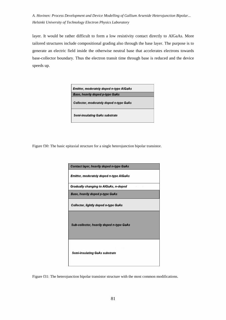
A. Hovinen: Process Development and Device Modelling of Gallium Arsenide Heterojunction Bipolar...
Helsinki University of Technology Electron Physics Laboratory
81
layer. It would be rather difficult to form a low resistivity contact directly to AlGaAs. More
tailored structures include compositional grading also through the base layer. The purpose is to
generate an electric field inside the otherwise neutral base that accelerates electrons towards
base-collector boundary. Thus the electron transit time through base is reduced and the device
speeds up.
Figure f30: The basic epitaxial structure for a single heterojunction bipolar transistor.
Figure f31: The heterojunction bipolar transistor structure with the most common modifications.

A. Hovinen: Process Development and Device Modelling of Gallium Arsenide Heterojunction Bipolar...
Helsinki University of Technology Electron Physics Laboratory
82
The epitaxial HBT structure is usually grown either using molecular beam epitaxy (MBE) or
metallo-organic vapour phase epitaxy (MOVPE). Traditional MOVPE uses silicon as donor
type dopant in GaAs, and zinc as acceptor type dopant in GaAs. MBE uses typically beryllium
for acceptor type doping in GaAs. Both zinc and beryllium diffuse relatively rapidly in GaAs,
and Zn redistribution during epitaxial growth with MOVPE has been a concern especially when
highly silicon doped layers are involved [r28]. When acceptor atoms diffuse from base to
emitter side, the pn-junction is shifted away from the heterojunction and the electrical structure
is destroyed. Also, it has been difficult to achieve electrically active acceptor concentrations
over 5.1018 cm–3 with MBE. During the last decade MBE technology has adopted carbon as the
acceptor type dopant in GaAs to suppress the diffusion problem. With carbon it is also possible
to dope the base up to 1020 cm–3 level. When beryllium or zinc is used as p-type dopant, a
spacer layer is usually added before heterojunction to prevent pn-junction shift. The spacer
layer width is determined empirically and is usually about 10 .. 20 nm.
3.2 Current Gain Simulation of the Example Structure
The optimisation of a spesific HBT structure for layer thickness and doping concentrations is
usually done with commercial computer sofware [r11]. If the transistor process is not well
parameterized like often is the case in laboratory experiments, basic one dimensional
calculations serve the purpose. One can then utilize simulation programs like PC-1D [r22], or
rely on semiconductor text books, e.g., [r29]. All the simulation examples in this thesis are done
with the matlab code generated by the author. Figure f32 shows an example of a real HBT
structure. The vertical dimensions of the layers are in scale to illustrate their relative
thicknesses. The dimensions are those that were used for the epitaxy of wafer “HBT02”
processed during the experimental part of this thesis. Other properties of the layers are
explained in Section 3.3.
The device in Figure f32 is a representation of an HBT in one dimension without external
electrical connections to the actual device terminals. Simulation is needed in determining the
proper doping concentrations for the layers before one could grow the epitaxial structure. For
initial simulations, the structure of Figure f32 was reduced to three layers by removing the
contact layers above emitter. The heterojunction grading was also removed, and the protective
layer was joined with base. The active area of the device was put to 400 µm2. The emitter AlAs
mole fraction x was put to 0,25. Bulk recombination lifetimes were τpe = 0,076 µs for emitter,
τnb = 0,0001 µs for base, and τpc = 0,34 µs for collector. Layer thicknesses for emitter, base and

A. Hovinen: Process Development and Device Modelling of Gallium Arsenide Heterojunction Bipolar...
Helsinki University of Technology Electron Physics Laboratory
83
collector were 1000 Å, 1100 Å and 6000 Å, respectively. Emitter doping was Ne = 5.1017 cm-3
and collector doping was Nc = 4.1016 cm-3 . With base doping of Nb = 3.1019 cm-3 the base-
collector depletion region edge was about 218 nm into collector. The energy band diagram of
the reduced structure with base doping of Nb = 3.1019 cm-3 was shown in Figure f6 with
discussion on band gap tailoring.
Figure f33 shows the simulated current gain of the transistor with base doping of 3.1017 cm-3.
Base-collector voltage was kept zero during simulation. Recombination effects were not
included. With this doping level the base is not yet degenerate. The current gain is over 500
although the base narrowing effect reduces gain as Vbe increases. Figure f34 shows the
simulated effect for increasing the base majority carrier concentration by two orders of
magnitude to 3.1019 cm-3. The simulated current gain is reduced to 50, which is still an
acceptable value for device application in amplifier circuits.
The actual epitaxial structure contains a grading layer between emitter and base that smoothens
the energy spike. The presence of a spike in conduction band increases the turn-on voltage of
the base-emitter diode. Vbe for 1kA/cm2 forward current density was about 1,35 V for the
structure of Figure f34. Proper smoothening of the spike should reduce the turn-on voltage for
about 150 mV [r16]. The effect of spike smoothening may be simulated by, e.g., giving a very
high value for the spike transparency γ in equation (e81) during simulations. Magnifying the
transparency for about 500 times or more during calculations yielded to turn on voltage of
about 1,245 V for the structure of Figure f34, with a slightly increased current gain.
Series resistance losses and two dimensional potential variations are not included in the core
equations. However, the importance of series resistance losses is acknowledged, and a simple
resistivity model is included into simulation code that calculates first estimates on resistive
losses across transistor layers for the user. These refinements are not included in the text of this
thesis.

A. Hovinen: Process Development and Device Modelling of Gallium Arsenide Heterojunction Bipolar...
Helsinki University of Technology Electron Physics Laboratory
84
Figure f32: An example of a real HBT structure.

A. Hovinen: Process Development and Device Modelling of Gallium Arsenide Heterojunction Bipolar...
Helsinki University of Technology Electron Physics Laboratory
85
Figure f33: Simulated current gain of the abrupt heterojunction structure with base doping of Nb = 3.1017
cm-3.
Figure f34: Simulated current gain of the abrupt heterojunction structure with base majority carrier
concentration increased by two orders of magnitude to 3.1019 cm-3. The gain is still over 50.

A. Hovinen: Process Development and Device Modelling of Gallium Arsenide Heterojunction Bipolar...
Helsinki University of Technology Electron Physics Laboratory
86
3.3 Epitaxial Layers in Detail
The early experimental work for this thesis was done with samples that were epitaxially grown
by H.U.T. Optoelectronics Laboratory. Samples that contained beryllium as base layer doping
were grown by A. F. Ioffe Physico-Technical Institute in St. Petersburg. Various epitaxial
constitutions were tried out during the process development while practical processing
knowledge was being gained. The epitaxial structure of wafer “HBT02”, represented in Figure
f32, is chosen here as an example. Although the layers are explained in detail, the overall
structure was not optimised to any spesific purpose but demonstration of the basic process. The
base layer was deliberately doped to very high level to avoid complications that may have
occurred due to excessive series resistance of the base contact. It was clear from previous
studies that ohmic contact optimisation may be tedious and time consuming [r09]. As a result of
high base doping, the current gain of the transistors was not expected to be higher than shown
in Figure f34. The emitter layer contained InGaAs capping to facilitate low emitter contact
resistance without extensive process optimisation. It was also recognized during the early stages
of process development that it would be rather difficult to achieve good ohmic contacts for both
emitter and collector simultaneously if the contact metal was kept the same for both terminals,
as was assumed during mask design [r27]. However, perfect ohmic contact in collector was not
essential for this thesis, and the collector contact was realised by a Schottky barrier which is
forward biased during forward active operation of the transistor. The layers that consitute the
processed HBT wafer are explained in detail below.
n+ (Si-doped) InGaAs contact layer, 5E18 cm-3, x=50%, 200 Angstroms
This layer is heavily doped and contains indium. Some ohmic contact processes introduce
indium to the contact during ohmic metallisation and the following heat treatment. InGaAs
capping introduces indium to the contact without alloying [r53]. Low resistivity contact
between the emitter and contact metal will be presumably due first to high silicon doping
enhancing the electron tunneling through the interfacial potential barrier and second because of
indium lowering the barrier by pinning the Fermi-level on the interface. In GaAs the pinning
position is roughly 0,8 eV below conduction band edge, and in pure InAs it is about 0,1 eV
inside the conduction band. With 50% of indium one has the pinning position in somewhere
between [r30].

A. Hovinen: Process Development and Device Modelling of Gallium Arsenide Heterojunction Bipolar...
Helsinki University of Technology Electron Physics Laboratory
87
n+ (Si-doped) InGaAs grading layer, 5E18 cm-3, graded roughly linearly, x=0.05 on
bottom, x= 50% on top, 500 Angstroms
This layer smoothens out the potential spike of In0,5Ga0,5As / GaAs interface and helps ruling
out the strain induced by the lattice mismatch. Without this layer the lattice mismatch would be
too much for epitaxial growth. Even with the grading layer present, In0,5Ga0,5As will be more or
less multicrystalline in nature [r52].
n+ (Si-doped), 5E18 cm-3, GaAs contact layer, 200 Angstroms
This layer also helps ruling out the spike. In simpler structures this layer is the contact layer for
metal, but then it would be much thicker to prevent ohmic metallisation penetration into
heterojunction area especially if gold-germanium based ohmic metallisation is used. For
shallow contacts, a Pd-In metallisation scheme could be used where InGaAs is formed to the
semiconductor surface during anneal [r31].
n+-AlGaAs grading layer, 2E18 cm-3, graded roughly linearly, x=25% on bottom,
x= 0.05 on top, 200 Angstroms
This layer smoothens out the potential spike in the interface between capping layer and emitter.
n-AlGaAs emitter, x=25%, 5E17 cm-3, 1000 Angstroms
This layer is the actual emitter.
n-AlGaAs grading layer, 5E17 cm-3, graded roughly linearly, x=0.05 on
bottom, x= 25% on top, 200 Angstroms
This layer helps smoothing out the potential spike between emitter and base. Without the
smoothing layer, the transistor emitter-base junction would need more forward bias to inject
electrons from emitter to base.

A. Hovinen: Process Development and Device Modelling of Gallium Arsenide Heterojunction Bipolar...
Helsinki University of Technology Electron Physics Laboratory
88
protective layer of undoped GaAs, 100 Angstroms
This layer prevents beryllium diffusion from base to heterojunction during epitaxial growth of
the upper layers. If the structure is heated excessively during the transistor processing or use,
this layer helps to minimise the performance reduction.
p+(Be-doped) GaAs base, 3E19 cm-3, 1000 Angstroms
This layer is the actual base. It is relatively thin to reduce electron transit time from emitter to
collector and heavily doped to keep the series resistance low. The doping level is enough to
turn the base degenerate. Although simple simulations in section 3.2. suggested that the doping
should be reduced for better current gain, it was kept high to make sure a tunneling contact
would be formed with base ohmic metal without need for high temperature alloying. With
thickness of 1000Å, the base transit time for an electron with saturation velocity of 2.105 m/s
would be about 0,5 ps. The diffusion transit time with a typical diffusivity of Db = 30 cm2/s
would be about 1,7 ps.
n- (Si-doped) GaAs collector, 4E16 cm-3, 6000 Angstroms
This layer is the collector. It is lightly doped to allow the pn-junction depletion region to be
wide thus reducing the base-collector capacitance. The maximum frequency of oscillation fmax
(or the power gain cut off frequency) of the transistor depends on the product of base series
resistance and base-collector capacitance. Reducing both will increase the transistor high
frequency performance. According to section 3.2., the depletion region depth in thermal
equilibrium will be about 218 nm. With a 400 µm2 device active are this gives base-collector
depletion capacitance of Cbc = 0,2 pF. Assuming a series resistance of 1 Ω, the charging time
constant of the capacitance would be 0,2 ps. To keep the charging time less than the diffusion
transit time of base, the collector series resistance should not exceed 10 Ω. Under normal
operation conditions of the transistor, b-c junction would be reverse biased and electrons are
accelerated to saturation velocity in the depletion region. An electron with saturation velocity
of 2.105 m/s would have the depletion region transit time of about 0,6 ps.

A. Hovinen: Process Development and Device Modelling of Gallium Arsenide Heterojunction Bipolar...
Helsinki University of Technology Electron Physics Laboratory
89
n+(Si-doped) GaAs sub-collector, 5E18 cm-3, 8000 Angstroms
This layer serves as the contact layer for collector.
Undoped GaAs buffer layer 2000 Angstroms
This layer helps keeping the defect density of the actual epitaxial structure low.
S.I. GaAs substrate 100 oriented
The substrate is semi-insulating. Crystal orientation is 100 to allow proper orientation of
transistor mesa isolation patterns with connection metal patterns. The correctly oriented mesa
hills will have positive slopes in the direction where metal connection wires enter the mesa hill.
This increases the reliability of the process as metal breaks are avoided.
3.4 Crystal Orientation
During conventional transistor processing the separate devices are electrically isolated from
each other by removing the conductive epitaxial layers between the devices. In Figure f30 this
means etching away the emitter, base and collector layers. The active devices look like hills, or
“mesas”, on a semi-insulating substrate. The height of a mesa is typically 1 ... 2 micrometers.
The mesas can be etched either by dry etching or wet chemical etching. In either case the two
important characteristics that need to be controlled over are the etching depth and the profile of
the etched mesa. In this HBT process the etching is based on citric acid and hydrogen peroxide.
The citric acid etching solution is made by adding 121 g of anhydrous citric acid crystals to
every 100 ml of deionised water [r09]. The crystals dissolve to water rather slowly, so the
solution is made preferably many days in advance the actual etching steps. The etching speed
for GaAs is controlled by adding a specific amount of hydrogen peroxide to the solution. 1 ml
of 31% H2O2 to every 100 ml of citric acid solution would give etching speed of roughly one
monolayer per second. The etchant temperature was kept on 20 0C.

A. Hovinen: Process Development and Device Modelling of Gallium Arsenide Heterojunction Bipolar...
Helsinki University of Technology Electron Physics Laboratory
90
The etchant is anisotropic in nature making the profile of a mesa hill to depend on its
orientation according to the wafer crystal lattice. Figure f35 shows how the mesa side slopes
are etched on a 100 oriented GaAs wafer with respect to the orientation flats. As a rule of
thumb, the direction of a smooth step over and thus the preferential entrance direction for a
metal wire to a mesa hill is perpendicular to the major flat of the 100 GaAs wafer.
During the processing of experimental HBT structures it is sometimes preferred to cut the wafer
to smaller entities before the actual processing to make several samples out of one wafer. It is
then important to be able to verify the correct orientation of the sample before the alignment
marks are made on the surface. An easy way to accomplish this is to etch rectangular test
patterns to the boundary areas of the sample by using, e.g. citric acid and hydrogen peroxide in
dilution of 10 : 1. Figure f36 shows the result after 15 min of etching. The etching depth was
about four micrometers. The proper orientation for metal wires would be on horizontal
direction for this sample. A small pin hole in the protecting layer would yield to a structure like
in Figure f37.
Figure f35: The mesa hill side slopes as etched on a 100 oriented GaAs wafer with respect to the
orientation flats.

A. Hovinen: Process Development and Device Modelling of Gallium Arsenide Heterojunction Bipolar...
Helsinki University of Technology Electron Physics Laboratory
91
Figure f36: Orientation etching result after 15 min on citric acid : H2O2 with 10 : 1 dilution. The proper
orientation for metal wires would be in horizontal direction.
Figure f37: Orientation etching through a pin hole in the protecting layer. The direction of the sample was
the same as in Figure f7.

A. Hovinen: Process Development and Device Modelling of Gallium Arsenide Heterojunction Bipolar...
Helsinki University of Technology Electron Physics Laboratory
92
3.5 Processing Steps
The processing steps for traditional HBT structures are explained in the following section. The
process is tailored for the set of equipment that were in use at Electron Physics Laboratory of
Helsinki University of Technology at the time of writing. Among the common laboratory
equipment, the most crucial apparatus was a properly calibrated profilometer (Dektak 3 by
Sloan Technology). It was used in verifying the correct etching depths for mesa patterns. Most
important for successful GaAs processing is to avoid any sources of unintentional scratches on
the periphery of the sample. If a scratch was there, a GaAs sample barely holds its own weight
when lifted up from corner. That is why every processing step was done using plastic tweezers
only. Fixing the sample to evaporation holder for metallisation or into a quartz boat for heat
treatment was done with extreme care. Any unnecessary “treatment” of the samples during the
process was avoided.
The basic HBT process developed for this thesis contains 9 mask levels including a mask for
alignment marks, 3 levels for mesa patterning, 3 levels for different kinds of metallisations, a
contact hole mask and a mask for passivation nitride pad openings. Additional mask levels that
were included to increase the process applicability were a mask level for patterning metal cross
overs in more complicated devices, and a mask level for patterning air bridge structures. The
basic lithography that was used for processing is explained in a separate booklet [r26]. The
design of a mask set should take into account that connection metal wiring is allowed to enter
the device mesa hill from the direction of smooth slopes of mesa hills only to avoid
metallisation breaks. Alternatively, air bridges should be used for entering the mesa hill.
The processing involves surface cleaning prior to any wet chemical etch or metal deposition. If
the surface contained any residuals prior to a wet chemical etch, the etching depth would differ
throughout the sample area. After storing an initially clean gallium arsenide sample for 4 days
in a shelf, the surface would contain about 30 Ångströms of different oxides of gallium and
arsenide [r32]. Arsenic oxides dissolve readily to water, and gallium oxides dissolve to alkaline
solutions but relatively slowly to acids [r33]. In this process uniform and repetitive wet
chemical etching was initiated by the following treatment:

A. Hovinen: Process Development and Device Modelling of Gallium Arsenide Heterojunction Bipolar...
Helsinki University of Technology Electron Physics Laboratory
93
Dip in deionised water for 5 seconds for wetting the surface.
Dip in mild ammonium for 30 seconds to attack gallium oxides. The dip contains one part of
25% ammonia solution (M=17,03g/mol, 1L = 0.91 kg) to 85 parts of deionized water.
Dip in deionised water for 5 seconds to dilute out ammonium from the sample.
Dip in 1:1 solution of hydrochloric acid and deionised water for 30 seconds.
Dip in deionised water for 5 seconds to dilute out HCl.
Wet chemical etching is then started immediately after the rinse. Another way of preparing the
surface would be to dip it on a strong HCl solution until the surface is hydrophobic.
3.5.1 Alignment marks
After verification of the correct alignment of the sample with respect to the mask, alignment
marks are patterned using the lift-off method tailored for AZ5214E-resist and AZ400K
developer. A Cr/Au-metallisation with 100Å of chromium and 500 ... 1000 Å of gold serves the
purpose. Chromium is used as an adhesion promoting layer between the surface and gold. This
mask level can be used also for patterning emitter contact metallisation for self-aligned base
metallisation scheme (SABM). Self aligned bases use emitter metallisation as etching mask of
emitter mesas. With wet chemical etching the emitter metal influences the etching process
(“galvanic effect”) making the method less controllable. In self aligned methods, dry etching is
preferred. The mask set for this thesis contained several SABM structures with emitter contact
metal depending on the choice of alignement metallisation. Galvanic effect seemed not to be a
concern with with Cr/Au emitter metal. Just prior to evaporation of metal, the sample surface
was cleaned by the method described above. If the cleaning was not successful, the alignment
pattern adhesion will fail either in ultrasonic cleaning during liftoff or successive processing
steps.

A. Hovinen: Process Development and Device Modelling of Gallium Arsenide Heterojunction Bipolar...
Helsinki University of Technology Electron Physics Laboratory
94
3.5.2 Emitter Mesa Pattern
The patterning is done with lithography tailored for AZ5214E and AZ 351B developer. The
lithography is finalised by a mild post bake in 120 0C for 30 min to make the resist boundaries
adhere more tightly to the surface. Without baking, the etchant would occasionally find its way
under the resist making the mesa periphery imperfect.
The emitter etching is initiated with the dip cleaning sequence described above. The etchant
solution consitutes of 1 ml of H2O2 in every 100 ml of citric acid solution. The etchant
temperature was 20 0C. This solution will attack the sample roughly one monolayer per second.
The etchant was made from pre-diluted citric acid liquid every time as it was needed, as the
actual amount of hydrogen peroxide would not have been controllable if the etchant was stored
long periods of time. It was proven very important to mix the etchant properly before use. The
citric acid liquid is rather viscous, and the hydrogen peroxide does not mix unless the etchant is
thoroughly stirred. The adhesion of AZ5214E resist would not hold against direct contact to
hydrogen peroxide. With epitaxial structure like in Figure f32, the target is to remove about
2400 Å of capping and emitter material while the underlying base layer is only about 1000 Å
thick. As the etchant is not selective between emitter and base layers, one has to be rather
careful not to etch excessively deep or to stay too low. Etching is best done in two steps,
making an intermediate measurement about the etching depth with profilometer from definite
check points, and adjusting the second etching time accordingly. After the resist removal, the
final etching depth is verified for future reference. Successful depth measurements call for
proper calibration standards with the profilometer apparatus. In this process the measurements
were done against a nominally 943 Å calibration standard with a certified systematic error of 15
Å at the day of calibration, December 19, 1996. The etching depth may be verified locally by
checking the breakdown voltage of a mechanical probe needle contact with exposed
semiconductor. Lightly doped n-type emitter would give a breakdown voltage in the order of 10
V, but heavily p-type doped base would be practically a short circuit [r14].
A. Hovinen: Process Development and Device Modelling of Gallium Arsenide Heterojunction Bipolar...
Helsinki University of Technology Electron Physics Laboratory
95
3.5.3 Base Mesa Pattern
The lithographic process for base mesa patterning is the same as for emitter mesas. The 2400 Å
emitter mesas are shallow as compared to the resist AZ5214E nominal thickness of 1,4
micrometers, so no planarisation is not yet needed. Post baking step should again be included.
Referring to Figure f32, the base mesa etch depth should be about 7000 Å, if the emitter mesa
etch was done accurately. Any discrepancies on emitter mesa depth should be taken into
account when etching the base mesa so that the sub-collector region is fully penetrated.
3.5.4 Emitter and Collector Ohmic Metal
After base mesa etch, the overall mesa hill will be about 8400 Å high with the structure as in
Figure f32. That is about half the nominal thickness of AZ5214E resist in the standard
lithography. The sample surface is planarised with the method described in reference [r26]
during the lithography to allow smooth step coverage and controlled line widths over mesa
regions. Post baking is not needed here. Prior to evaporation of ohmic metal, the surface oxides
need to be removed. The dipping as described before may be used, preferably assisted with a
short ion milling step prior to evaporation.
One of the important figures of merit of an HBT is the maximum frequency of oscillation fmax .
It is maximised if the transistor active area is kept minimal. This calls for a very small area
emitter. Typically, the emitter may be just a few micrometer square. Still, the emitter should be
able to supply the transistor bias current without excessive series resistance loss. This translates
to an extremely low resistance ohmic contact. With specific contact resistance of 1.10-6 Ωcm2,
an emitter with one square micrometer area would have a series resistance of 100 Ω. With a
bias current of 10 mA this would generate voltage drop of 1 V. For this thesis the emitter and
collector ohmic metallisations were done simultaneously. The contact needs to be shallow in
nature to prevent ohmic metal from penetrating the heterojunction. In GaAs-MESFET
technology n-type layers are often contacted using eutectic gold-germanium (AuGe) based
alloyed contacts that may penetrate several thousands of Ångströms into GaAs [r34]. AuGe is
thus avoided in HBT designs with shallow emitters.

A. Hovinen: Process Development and Device Modelling of Gallium Arsenide Heterojunction Bipolar...
Helsinki University of Technology Electron Physics Laboratory
96
HBT structures without InGaAs-capping layer in emitter may use, e.g., Pd-In-based contact
metallisations [r31]. With InGaAs layer included, a tri-layer of nonalloyed Ti/Pt/Au is often
used to form a tunnelling contact. Ti serves as an adhesive and Pt prevents gold from diffusing
into the semiconductor. The evaporation may be preceded by in-situ Ar+ ion bombardment to
remove the interfacial oxides from the surface. Specific contact resistances in 10-8 Ωcm2 range
have been achieved with the ion bombardment method [r35]. Using a Pd/Ge bilayer, shallow
contacts to InGaAs with specific contact resistances in 10-7 Ωcm2 range have been
demonstrated [r36]. For simple needs, a Cr/Au contact metal might be enough [r37], [r38]. Here
chromium serves as an adhesion promoter between the sample surface and gold layer.
Additionally, it should prevent gold and gallium from intermixing during subsequent heat
treatments. Gold and gallium form liquid phases at temperatures over about 340 0C, as can be
seen from the Au-Ga phase diagram in Figure f38 [r39]. With arsenic a liquid phase is found at
about 640 0C. It is thus of crucial importance that direct contact with Au and GaAs surface is
avoided if one wishes to maintain shallow ohmic contacts during any heat treatment.
The collector contact has typically much more area than emitter, and low contact resistance is
not as important. Sometimes the collector contact is accomplished by a Schottky diode. A
Schottky diode in transistor collector junction would be forward biased during the normal
operation of transistor. GaAs-based Schottky diodes are very fast and do not affect the
transistor high frequency performance [r08]. In this thesis, both emitter and collector contact
areas were defined in a single mask step, and the collector contact formed a Schottky diode
with properties that were dependent on the metallisation choice done in favour for reducing
emitter contact resistivity. Electron beam evaporation of metals like Pt, Ti, or Pd may need a
rather heavy beam current. In that case there is a risk of burning the resist while evaporating.
Burned resist could in principle be removed with oxygen plasma, but at least with the
equipment in our laboratory that took a very long time, and the sample was generally heated
strongly during the treatment. Especially with fast diffusing dopant atoms like zinc or beryllium
in the HBT base layer, heating over a few hundred degrees Celsius for extended period of time
would be bad for the heterostructure. Usually, if the resist burned, the sample was considered to
be lost. In some extreme cases a quick recovery trial may be applicable. Treating the sample
with undiluted AZ400K developer in ultrasonic bath may lift off the resist in some minutes. If
so, the sample surface is then finished with a relatively short oxygen plasma etch.

A. Hovinen: Process Development and Device Modelling of Gallium Arsenide Heterojunction Bipolar...
Helsinki University of Technology Electron Physics Laboratory
97
Figure f38: The phase diagrams of Au-As and Au-Ga systems [r39].

A. Hovinen: Process Development and Device Modelling of Gallium Arsenide Heterojunction Bipolar...
Helsinki University of Technology Electron Physics Laboratory
98
The ohmic metallisation is usually finalised by rapid thermal anneal. If the anneal was similar
to the base ohmic metallisation, they are then preferably done simultaneously. While annealing
GaAs, one should recall that GaAs surface decomposes in temperatures exceeding about 6000C. To prevent arsenic atoms from escaping the surface during anneal, a silicon nitride capping
layer is sometimes used with high temperature anneals. For this thesis the annealing
temperatures were kept lower than 550 0C to minimise the decomposition problem.
3.5.5 Base Ohmic Metal
The base ohmic metal patterns are defined before etching collector mesas to benefit from the
more shallow mesa hill. Lithography is of planarising type and similar to the previous step.
Prior to evaporation of ohmic metal, the surface oxides need to be removed. With heavily p-
type doped GaAs base, a typical choice for contact metallisation is Ti/Pt/Au [r35], [r40]. If the
base layer was graded to reduce the carrier transit time, a Pt/Ti/Pt/Au metallisation may be
adopted to facilitate contact formation to presumably oxidised AlGaAs surface of base [r41]. If
the base layer was thick enough, also AuBe or AuZn alloys have been used. On evaporation of
alloy material one should recall that resistive evaporation will not yield to homogenous metal
film with material ratio of the source because of difference in evaporation rates of metals.
Resistive evaporation may be applicable only if all of the source material is evaporated at once
and the metal film was remixed during subsequent anneal. Alloyed source material is best
evaporated using electron beam evaporation method. As an example, e-beam evaporation of
AuZn alloy with 5 %wt Zn from a carbon crucible resulted a film of AuZn with 3,9 %wt Zn
according to RBS measurement. Because of the carbon crucible, the film contained also about
5%at carbon.
3.5.6 Collector Mesa Pattern
Lithography here is of planarising type, and tailored for mesa etching. Post baking is again used
to prevent the etchant from finding its way under the resist pattern making the mesa periphery
imperfect. From Figure f32, the etching depth would be 8000 Å. After etching the devices
should become isolated electrically. This may be verified by probe measurement on defined test
points on the chip.

A. Hovinen: Process Development and Device Modelling of Gallium Arsenide Heterojunction Bipolar...
Helsinki University of Technology Electron Physics Laboratory
99
3.5.7 Insulation
After collector mesa etch the sample is ready to be coated with insulating material. In this
process the insulation is accomplished by plasma enhanced chemical vapour deposited
(PECVD) silicon nitride. During deposition the sample is kept at 300 0C temperature. The
thickness of deposited insulation was typically 150 nm.
3.5.8 Contact Holes
In this process the contact hole pattern in the mask consists of 2 µm x 2 µm holes with 2 µm
separation. The area that is to be contacted is filled with the dot pattern. Lithography is again of
planarising type, tailored for contact hole patterning. After development, the contact holes on
the resist will look like round circles. The hole pattern is then transferred to silicon nitride
insulation layer by chemical plasma etching (CPE) with sulfur hexa fluoride (SF6). Figure f39
shows a SEM picture of an HBT just after opening the contact holes through nitride. The grainy
contact metal is seen through the contact holes.
Figure f39: An HBT after contact hole etching step.

A. Hovinen: Process Development and Device Modelling of Gallium Arsenide Heterojunction Bipolar...
Helsinki University of Technology Electron Physics Laboratory
100
3.5.9 Wiring Metallisation
Wiring metallisation connects the device terminals with their contact pads. In some processes
the semiconductor surface is planarised by, e.g., polyimide coating before wiring lithography.
In this process the planarisation for wiring lithography is accomplished by a double layer of
resist AZ5214E. Both resist layers may be patterned separately to form, e.g. air bridge
structures. Similar kind of double layer lithography scheme was used with MPR1470 resist by
Kazuhiko, T., et al. in reference [r42]. Wiring metallisation patterning is the most demanding
lithography step on this process. While being planarising, the lithography has to maintain good
line width control simultaneously on mesa regions (shallow resist) and field areas (thick resist).
Yet the resist profile has to maintain a shape that is suitable for lift-off metallisation. In this
process the metallisation is typically Cr/Au with 100 Å of chromium and 3000 Å of gold. For
applications where the resistance of connector wiring is a concern, the wiring metal is made
thicker. Preliminary tests on using electroless plating of copper in strengthening of the wiring
metallisations were also examined as future addition to the process with encouraging results.
Plating studies were not included in this thesis to avoid excessive divergence of the subject.
Figure f40 gives an example of wiring into a transistor structure. The base contact in this
example was split in two and connected together with a wiring metal crossover. Entrance to
mesa hill was done by air bridges for emitter and base.
Figure f40: A transistor with a split base contact and air bridges in wiring metal.

A. Hovinen: Process Development and Device Modelling of Gallium Arsenide Heterojunction Bipolar...
Helsinki University of Technology Electron Physics Laboratory
101
3.5.10 Passivation
The insulation formed in step (3.5.7) shields the devices against contamination while forming
the dielectric for capacitor structures. The final passivation step is included here to give the
wiring metallisation in field areas of the sample mechanical shield against scratches. The
passivation layer is again of silicon nitride. It should be noted that the scratch shield is not
enough to protect the active areas of the sample, especially if the structures include air bridges.
Care has to be taken in order not to ruin the samples mechanically before encapsulation. The
samples do not survive if they were occassionnally flipped over on a flat surface.
3.5.11 Pad Opening
This step forms openings over contact pads and is made the same way as contact holes were
made in step (3.5.8). After this step the sample is ready for probe measurements or wire
bonding and packaging.
3.6 Naming Convention of the Processed Devices
All the processed devices were named with a self consistent manner in order to keep track of
the various measurements and experiments that were done to the processed devices. The
process runs were numbered cumulatively, and sample in runs were named alphabetically, e.g.,
A, B, and C. The chips on each processed samples were numbered by position on the sample,
and each structure on the chip was number by the position in the chip. The name of a specific
structure was then constructed by run, chip and structure type. For example, name HBT02-
C:2403 refers to process run 2, sample C, chip 24 and structure 3. To maintain consistency, the
naming convention is preserved in the Figures of this thesis for easy identification of the
structure under study.

A. Hovinen: Process Development and Device Modelling of Gallium Arsenide Heterojunction Bipolar...
Helsinki University of Technology Electron Physics Laboratory
102
3.7 Test Structure with Loose Tolerance Design
Transistor geometry has to be optimised for high speed operation. Any stray capacitance and
series resistance or inductance should be minimised. Figure f41 shows an illustrative example
of an HBT layout with no special optimisation. This is the “loose tolerance” test structure from
the basic HBT mask set. The emitter mesa size was 20 µm x 20 µm. There is no air bridge
under the emitter wire for smooth entrance to emitter mesa over the boundaries. Only the
preferential slope on mesa boundaries prevents the wire from breaking up.
The active region of the transistor is under the emitter mesa. Electrical path between the base
contact and active region is relatively long and resistive. Self aligned base metallisation
processes (SABM) would help reducing this parasitic base series resistance. A trial SABM
process is included in the mask set. Also, the base surface is vastly exposed provoking surface
recombination. Usually, if the base surface was exposed, it would be passivated, e.g., using a p-
doped AlGaAs capping layer that repels charge carriers from the surface [r30]. As the surface
recombination current is suppressed, the total base current that is needed for transistor biasing
to operation point is reduced.
Not shown in the picture are the respective contact pads for emitter, base and collector.
Additional series resistance will be generated by the resistivity of wiring itself. Although of
gold, the wiring metal has to be thick and wide enough to minimise the series resistances. In our
experience, the measured resistivity of e-beam evaporated gold wiring of 100 nm thickness was
about four times the bulk value of gold. A 10 µm wide wire of 100 µm length and 100 nm
thickness would then have a series resistance of 9,4 Ω. Finally, base and emitter wires have to
travel on top of collector mesa for quite a long way with 150 nm of nitride isolation in between.
Thus a considerable capacitance is formed between the legs of the transistor in addition to the
intrinsic capacitances. Although of no use in applications, this example structure is good in
checking out the parasitics of the transistor process. Loose alignment tolerances allow the
structure to function electrically even with relatively huge alignment errors during the process.
As a consequence, it has been usually the first structure that is tested out after an experimental
HBT process.

A. Hovinen: Process Development and Device Modelling of Gallium Arsenide Heterojunction Bipolar...
Helsinki University of Technology Electron Physics Laboratory
103
Figure f41: SEM picture of an HBT structure with loose tolerance design.
3.8 Choice of Contact Metallisation Material
Various ohmic metal compositions were examined during the early efforts of process
development [r27]. The first transistor structures were with Zn-doped base layer and Pd/In-
ohmic contacts for emitter and collector. InGaAs emitter capping was not yet present. The base
contact was AuZn-based. The first structures showed rather poor DC characteristics with
current gain barely exceeding unity. It was found out that the samples were very sensitive to
heat treatment, and emitters were typically corrupted before ohmic contacts were formed during
rapid thermal anneal. The emitter layers were then redesigned to include InGaAs capping, and
any heat treatment other than implicit in, e.g., PECVD nitridation and e-beam evaporation was
avoided. A very simple metallisation with Cr/Au on every contact was chosen as a base line
reference (sample A). The epitaxial structure was as described in section 3.3. It was expected
that emitter should have a fairly good ohmic contact with Cr/Au because of InGaAs capping.
The Cr/Au -base contact should also become ohmic because of tunneling effect. Collector
contact would be a more or less leaky Schottky diode which should not hinder the transistor
operation, as the diode would be forward biased in normal transistor operation. Reverse
Gummel plots would be severely affected because of the diode.
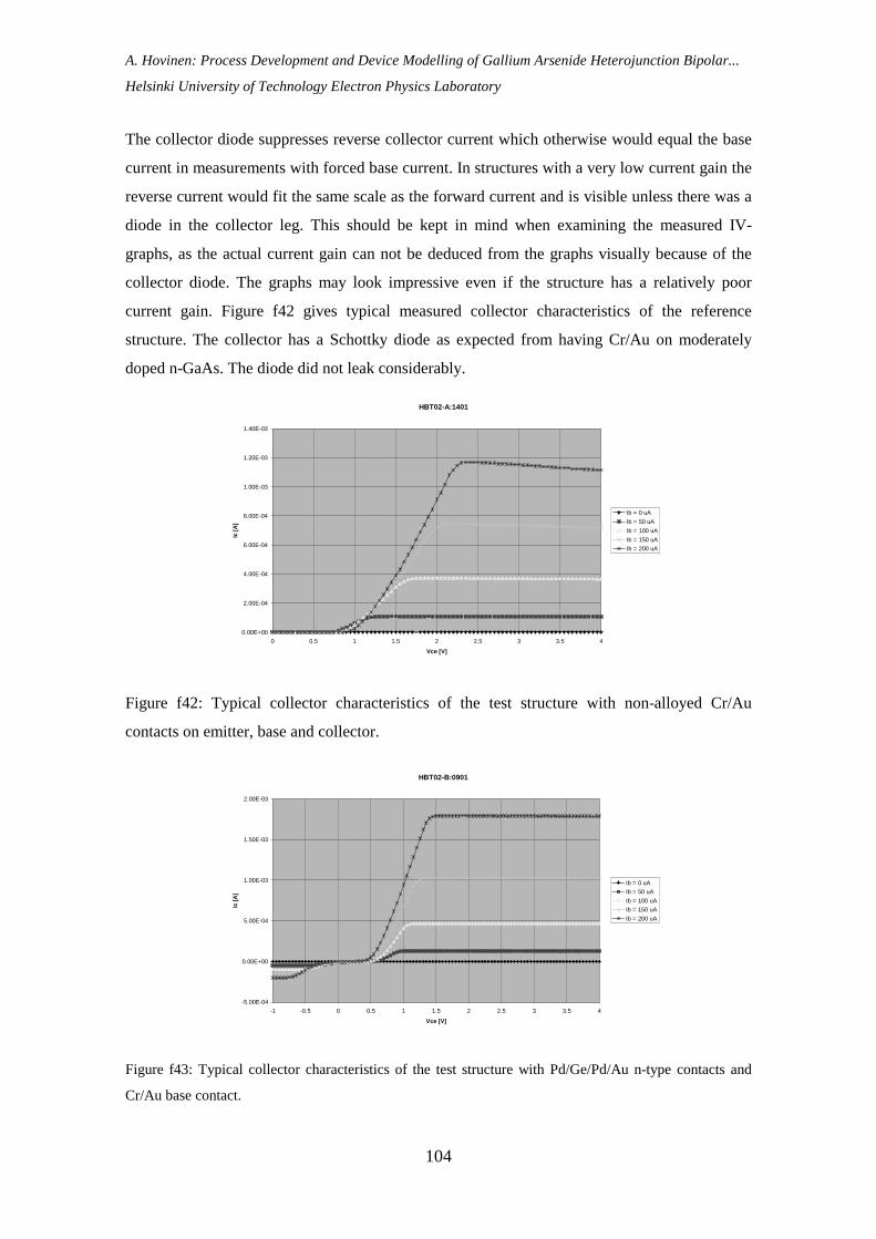
A. Hovinen: Process Development and Device Modelling of Gallium Arsenide Heterojunction Bipolar...
Helsinki University of Technology Electron Physics Laboratory
104
The collector diode suppresses reverse collector current which otherwise would equal the base
current in measurements with forced base current. In structures with a very low current gain the
reverse current would fit the same scale as the forward current and is visible unless there was a
diode in the collector leg. This should be kept in mind when examining the measured IV-
graphs, as the actual current gain can not be deduced from the graphs visually because of the
collector diode. The graphs may look impressive even if the structure has a relatively poor
current gain. Figure f42 gives typical measured collector characteristics of the reference
structure. The collector has a Schottky diode as expected from having Cr/Au on moderately
doped n-GaAs. The diode did not leak considerably.
Figure f42: Typical collector characteristics of the test structure with non-alloyed Cr/Au
contacts on emitter, base and collector.
Figure f43: Typical collector characteristics of the test structure with Pd/Ge/Pd/Au n-type contacts and
Cr/Au base contact.
HBT02-B:0901
-5.00E-04
0.00E+00
5.00E-04
1.00E-03
1.50E-03
2.00E-03
-1 -0.5 0 0.5 1 1.5 2 2.5 3 3.5 4
Vce [V]
Ic [
A]
Ib = 0 uA
Ib = 50 uA
Ib = 100 uA
Ib = 150 uA
Ib = 200 uA
HBT02-A:1401
0.00E+00
2.00E-04
4.00E-04
6.00E-04
8.00E-04
1.00E-03
1.20E-03
1.40E-03
0 0.5 1 1.5 2 2.5 3 3.5 4
Vce [V]
Ic [
A]
Ib = 0 uA
Ib = 50 uA
Ib = 100 uA
Ib = 150 uA
Ib = 200 uA

A. Hovinen: Process Development and Device Modelling of Gallium Arsenide Heterojunction Bipolar...
Helsinki University of Technology Electron Physics Laboratory
105
Another sample was prepared with Pd/Ge/Pd/Au n-type contacts and Cr/Au base contact
(sample B). The typical collector characteristics is shown in Figure f43. The negative currents
were already partially visible, although the contacts were not fully ohmic. It is probable that a
moderate anneal for this structure before PECVD step would have formed an ohmic contact to
collector. Typical current gain was about 10. Some transistors on the sample showed current
gains exceeding 30 because of process variations.
An effort to make a sample with Pd/AuGe/Ag/Au n-type contacts and Ni/AuZn base contact
was also done (sample C). During e-beam evaporation of nickel the sample was over heated to
an undetermined temperature and the resist was burned. The temperature exceeded AZ5214E
resist burning limit of 120OC for several minutes. The sample was treated with the AZ400K
method as described in paragraph 4.4. As a co-incident, the collector ohmic metal adhesion was
found to be rather poor and it was ripped off during ultrasonic bath. Thus, even though there
was no separate mask levels for emitter and collector ohmic contacts, it was possible to test out
a method of making the collector contact directly with wiring metal Cr/Au through contact
holes, presumably with some residuals of Pd on the collector surface. Also, the emitter contact
had been unintentionally moderately heated by the failed Ni deposition. The opportunity
encouraged to proceed the experiment forward even though the sample was considered lost.
The typical collector characteristics of the test structure is shown in Figure f44. The structures
performed very good as compared to basic structure of Figure f42. From the Figure f44 it is
seen that the slope of the curves are very steep, suggesting acceptably small series resistance on
emitter and collector contacts. The collector contact was a diode. In the current range of Figure
f44 the measured current gain was again about 10. The current gain of an HBT may increase
with the collector current density. Low series resistance in this sample allowed the
measurements to be done with more heavy current level without excessive resistive voltage
drops. Figure f45 shows the transistor collector characteristics for base current up to 600 µA.
The current gain approached 40 with collector current level of 20 mA.
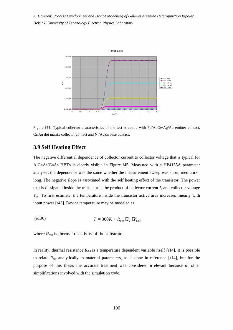
A. Hovinen: Process Development and Device Modelling of Gallium Arsenide Heterojunction Bipolar...
Helsinki University of Technology Electron Physics Laboratory
106
,300 0 CEcth VIRKT ⋅⋅+=
Figure f44: Typical collector characteristics of the test structure with Pd/AuGe/Ag/Au emitter contact,
Cr/Au dot matrix collector contact and Ni/AuZn base contact.
3.9 Self Heating Effect
The negative differential dependence of collector current to collector voltage that is typical for
AlGaAs/GaAs HBTs is clearly visible in Figure f45. Measured with a HP4155A parameter
analyser, the dependence was the same whether the measurement sweep was short, medium or
long. The negative slope is associated with the self heating effect of the transistor. The power
that is dissipated inside the transistor is the product of collector current Ic and collector voltage
Vce. To first estimate, the temperature inside the transistor active area increases linearly with
input power [r43]. Device temperature may be modeled as
(e136)
where Rth0 is thermal resistivity of the substrate.
In reality, thermal resistance Rth0 is a temperature dependent variable itself [r14]. It is possible
to relate Rth0 analytically to material parameters, as is done in reference [r14], but for the
purpose of this thesis the accurate treatment was considered irrelevant because of other
simplifications involved with the simulation code.
HBT02-C:2601
0.00E+00
5.00E-04
1.00E-03
1.50E-03
2.00E-03
2.50E-03
-1 -0.5 0 0.5 1 1.5 2 2.5 3 3.5 4
Vce [V]
Ic [
A]
Ib = 0 uA
Ib = 50 uA
Ib = 100 uA
Ib = 150 uA
Ib =200 uA

A. Hovinen: Process Development and Device Modelling of Gallium Arsenide Heterojunction Bipolar...
Helsinki University of Technology Electron Physics Laboratory
107
Figure f45 shows the measurement result of a transistor with constant base current stimulus.
Device simulations should also be done in constant base current mode, letting base voltage to
drift as the device heats up. The voltage drop over collector Schottky diode should also be
taken into accunt in the simulation to properly estimate power load of the actual transistor. In
paragraph 2.13 it was briefly mentioned that constant base current simulations constitute of
massive iteration of the device equations, as the equations are not analytically solvable for Vbe.
Figure f46 shows the result of constant base current simulation for a transistor with doping
concentrations and layer thicknesses as in the actual measured transistor, and with numerical
value of Rth0 = 500 K/W. Base current level was stepped according to the insert of figure f45.
The numerical value of the thermal resistance was chosen after some initial iteration for proper
slope in the IV-curve, and represents a typical value [r14], [r56]. The simulation was based on
thermionic emission theory, excluding the electrons that would tunnel through the conduction
band spike. To include the spike transparency calculation within the iteration loop, the
simulation code needs still some refinement not to overload the computer memory. Also
included in the simulation was a rough model for the observed collector diode to take into
account the diode voltage drop in the collector current path. Diode model parameters were IS =
1.10-12 A for saturation current, n = 2 for ideality factor, RS = 1 Ω for series resistance and RSH =
1MΩ for shunt resistance. The self heating effect in collector current is readily seen from the
simulation result of Figure f46. More accurate fit to the measured curve may be obtained after
inclusion of thermionic field-emission theory into calculations, after which a better diode
modelling may also become relevant. It is seen from Figure f46 that simple thermionic model
gives qualitative information on the self heating effect of the transistor under study. It is worth
mentioning that the simulated effect relies on proper modelling of band discontinuities between
emitter and base. Equations (e13) were used in determining the band structure in the
simulations for this thesis.

A. Hovinen: Process Development and Device Modelling of Gallium Arsenide Heterojunction Bipolar...
Helsinki University of Technology Electron Physics Laboratory
108
Figure f45: The transistor of Figure f44 with base current levels up to 600 uA. The resulting current gain
was about 40 with collector current level of 20 mA.
Figure f46: One dimensional constant base current simulation of the transistor with temperature effects,
showing clearly the negative differential dependence of collector current to collector voltage. Doping
concentrations and layer thicknesses were as in the actual measured transistor. Numerical value for
thermal resistance was Rth0 = 500 K/W. Base current level was stepped according to the insert of figure
f45.
HBT02-C:2601 April 1, 2000 A. Hovinen
0.00E+00
5.00E-03
1.00E-02
1.50E-02
2.00E-02
2.50E-02
0 1 2 3 4 5 6
Vce [V]
Ic [
A]
Ib = 0 uA
Ib = 150 uA
Ib = 300 uA
Ib =450 uA
Ib = 600 uA
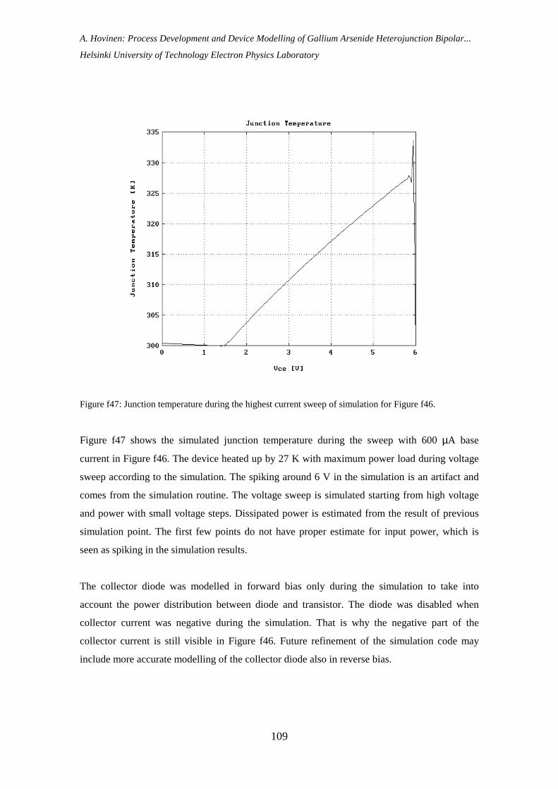
A. Hovinen: Process Development and Device Modelling of Gallium Arsenide Heterojunction Bipolar...
Helsinki University of Technology Electron Physics Laboratory
109
Figure f47: Junction temperature during the highest current sweep of simulation for Figure f46.
Figure f47 shows the simulated junction temperature during the sweep with 600 µA base
current in Figure f46. The device heated up by 27 K with maximum power load during voltage
sweep according to the simulation. The spiking around 6 V in the simulation is an artifact and
comes from the simulation routine. The voltage sweep is simulated starting from high voltage
and power with small voltage steps. Dissipated power is estimated from the result of previous
simulation point. The first few points do not have proper estimate for input power, which is
seen as spiking in the simulation results.
The collector diode was modelled in forward bias only during the simulation to take into
account the power distribution between diode and transistor. The diode was disabled when
collector current was negative during the simulation. That is why the negative part of the
collector current is still visible in Figure f46. Future refinement of the simulation code may
include more accurate modelling of the collector diode also in reverse bias.

A. Hovinen: Process Development and Device Modelling of Gallium Arsenide Heterojunction Bipolar...
Helsinki University of Technology Electron Physics Laboratory
110
4 Practical Measurements
4.1 Analysis environment
The main apparatus for direct current measurements of the test structures was HP 4155A
parameter analyser with ICS Interactive Characterization Software by Metrics Technology.
The apparatus was situated inside the H.U.T. clean room, which in essence is a Faraday cage
with several high power radio frequency transmitters like PECVD inside. The measurements
that needed low levels of environmental noise were done with HP4145 measurement setup
outside the clean room.
Light sensitivity of the structures under “on wafer” study were examined as part of device
probe measurements. Illuminated HBT is a photodetection device. The applicability of
heterojunction devices in the field of high speed photodetection has gained growing interest
during last decade. It was shown by Suematsu and Ogawa in [r44] that HBT–based
photodetection is a competitive alternative to PIN-diode based photodetection in high speed
applications. The absorption coefficient of intrinsic GaAs at room temperature for photons with
energy exceeding the forbidden band gap width of 1,42 eV is about 104 cm-1 [r45]. This
corresponds to absorption depth of about one micrometer. On the exposed areas of Figure f41
the photons are thus absorbed effectively by the base layer of 1000Å thickness and collector
layer of 6000Å thickness. There is a finite spatial collection probability of generated electron-
hole pairs for the reverse biased collector-base junction beneath the neutral base layer [r46].
Absorption in the neutral base layer increases the excess minority electron concentration,
which reduces electron emission through heterojunction in low bias conditions reducing the
phototransistor gain performance [r47]. Some of the electrical measurements were repeated
under illumination to gain information on the severity of light pollution on the device
measurements.

A. Hovinen: Process Development and Device Modelling of Gallium Arsenide Heterojunction Bipolar...
Helsinki University of Technology Electron Physics Laboratory
111
4.2 Connecting the Device to measurement
DC measurements were performed on manual probe stations with Tungsten needles. The series
resistance over a needle tip during measurements was typically 4 Ω per needle according to
short circuit measurements that were routinely performed before any transistor testing.
Measurement pad connections were 100 µm x 100 µm squares. The pad metallisation was the
same as used in wiring layer, typically 300 nm gold on 10 nm chromium. Scratching a contact
pad during needle probing is inavoidable with the metal thicknesses of 300 nm or less. A device
could typically be needle probed two or three times before the pad connection failed.
Some of the devices were wire bonded for more permanent study. Model UZS.M-2.5 ultrasonic
welding machine with 25 µm diameter aluminum wire was used. Processing of the
measurement pad metallisation was not yet optimised for ultrasonic bonding, which allowed the
bonding operation to become rather destructive. Typical bonding associated failure was metal
rip off under the area of bonding, which could have been avoided by thicker pad metallisation.
In some cases it was seen that improper cleaning of the silicon nitride surface prior to pad
metallisation resulted in adhesion failure of the pad. The surface under bonding pads was not
pretreated to promote adhesion. In forecoming processing efforts the pad metallisation should
be refined to make wire bonding feasible. In this thesis the low yield of wire bonding step was
not a concern, and transistors in a chip were ruined rather nonchalantly until a satisfactory
bonding was achieved. Typically 5 devices were lost for every succesfully wire bonded device.
4.3 Extracting Equivalent Circuit Parameters from Measurements
Gummel plot is a tool for extracting transistor DC parameters for base and collector current.
The Gummel measurement is performed by sweeping VBE across the safe operation area of the
device while keeping VCB zero, and measuring terminal currents. Light sensitivity of the device
may be seen from the low current region of the Gummel plot. Figure f48 compares room
temperature measurement results of a device in dark and as illuminated by probe station
microscope light. The non-zero measured current level of 30 pA in dark at zero base-emitter
voltage is an indication of the systematic measurement error level of the measurement
apparatus, not actual device current. It is seen that illumination generated about 3 nA “short
circuit” current in the base-collector circuit.

A. Hovinen: Process Development and Device Modelling of Gallium Arsenide Heterojunction Bipolar...
Helsinki University of Technology Electron Physics Laboratory
112
Also shown in Figure f48 is the result of exponential fit of the base and collector currents of the
transistor under study. According to the fit, base current obeys ideal diode law with saturation
current Is,base = 4.10-15 A and ideality factor nbase = 1,935. Device emitter area was 10 x 50 µm.
Collector saturation current was Is,collector = 2.10-23 A and ideality factor ncollector = 1,067. The
ideality factors indicate that base current was mainly of space charge recombination current
type, and collector current was of diffusion current type [r13]. The measurement also reveals
that the device gain barely exceeded unity at current levels of 1 mA. This was because the
rectifying collector contact was not forward biased during the measurement with VCB = 0V.
Figure f49 shows a collection of Gummel plot measurement data of another transistor from the
same chip. Device are emitter area was 6 x 26 µm. This time the base-collector voltage VCB was
varied according to the insert of Figure f49. It was observed during measurements that
illumination did not affect considerably the collector current when VCB was over 1V. However,
currents measured in dark were seemingly swapped. Dark base current curve matched with the
collector current curves with VCB offset at high VBE, and dark collector current matched with
base current curves, although not as smoothly. The seemingly confusing result was related to
non-ohmic collector contact, and was later verified with Spice-based simulations. The constant
collector current with low VBE bias came from leakage between base and collector. The leakage
current dominated over “photocurrent” when VCB was over 1 V. The distance between flat parts
of the current sweeps is roughly constant in logarithmic scale, indicating that the leakage
current obeys exponential law. Fit to measurement data at VBE = 0,6 V gave leakage diode
parameters Is,leakage = 5.10-11 A for saturation current, and nleakage = 11,316 for ideality factor. The
high value of n indicates that voltage was actually not constant over the area of leakage, but in
average only a small fraction of VCB. High values of n are sometimes also justified, e.g., with
recombination by series effect of tunneling through a potential barrier and recombination via
junction interface recombination centers rising tunneling-recombination leakage current with
ideality factor n approaching 4 in room temperature [r14].

A. Hovinen: Process Development and Device Modelling of Gallium Arsenide Heterojunction Bipolar...
Helsinki University of Technology Electron Physics Laboratory
113
Figure f48: Gummel plot measurement of a transistor acting as a “photodetector”. Note that negative
current data from measurement under illumination is converted to absolute value in order to be seen in
logaritmic scale. Device emitter area was 10 x 50 µm
Figure f49: A collection of Gummel plot measurement data of transistor HBT02-B:2403. Device emitter
area was 6 x 26 µm. The leakage of base-collector diode is readily identified from the plot.
HBT02-B:2403Gummel plot dependence on Vcb offset voltage
and microscope light
y = 1E-15e20.565x
y = 2E-23e36.2x
1.00E-11
1.00E-10
1.00E-09
1.00E-08
1.00E-07
1.00E-06
1.00E-05
1.00E-04
1.00E-03
1.00E-02
0 0.5 1 1.5 2 2.5
Vbe [V]
Ib, I
c [A
]
Ib (dark)
Ic (dark)
Ib (offset 1 V)
Ic (offset 1 V)
Ib (offset 2 V)
Ic (offset 2 V)
Ib (offset 3 V)
Ic (offset 3 V)
Ib (offset 4 V)
Ic (offset 4 V)
Ib ( light on)
Ic (light on)
Ib dark fit 1
Ic dark fit
Expon. (Ib dark fit 1)
Expon. (Ic dark fit)
HBT02-B:2402Gummel with Vcb offset = 0 V. Light dependence.
y = 2E-23e36.26x
y = 4E-15e19.987x
1.00E-12
1.00E-11
1.00E-10
1.00E-09
1.00E-08
1.00E-07
1.00E-06
1.00E-05
1.00E-04
1.00E-03
1.00E-02
1.00E-01
1.00E+00
0 0.5 1 1.5 2 2.5
Vbe [V]
Ib, I
c [A
]
Ib (dark)
Ic (dark)
abs(Ib) with light on
abs(Ic) with light on
Ic fit
Ib fit
Expon. (Ic fit)
Expon. (Ib fit)

A. Hovinen: Process Development and Device Modelling of Gallium Arsenide Heterojunction Bipolar...
Helsinki University of Technology Electron Physics Laboratory
114
Attempts to model the leakage current as reverse leakage across base-collector junction failed
because of the distributed nature of the leak. The exponential dependence of leakage current on
applied voltage VCB ruled out generation current JgC in the junction depletion region as a
possible cause, although the direction of leakage current could support the assumption.
Presumably the leak originated from surface effects. PECVD deposited silicon nitride does not
passivate GaAs surface efficiently, and it is conceivable that base minority electrons and
collector minority holes in the vicinity of base periphery may leak by the sides of the pn-
junction using the surface channels in the periphery [r48]. The observed “photocurrent” in
nanoampere scale may also be considered as periphery leak current instead of short circuit
current of collector junction acting as a solar cell, for the simple reason that series resistances
in the circuit blocked out the concept of a short circuit. Instead, the illumination increased the
potential difference between base and collector layers by solar cell action to approximately 1 V
level, which in turn made leaking to occur under illumination. The measurement apparatus kept
external VCB at 0V, while the light-induced voltage difference was over the reverse biased
rectifying contact of collector. It may be concluded that the device process should include
effective surface passivation if devices with perimeter of 6 x 26 µm or less are to be processed
with intention to reach controllable collector operation under 100 µA level at VCB of several
volts.
Also shown in Figure f49 is the result of fitting the base and collector currents to ideal diode
law. The base current may be modeled with Is,base = 1.10-15 A and ideality factor nbase = 1,881.
Emitter diode characteristics were also measured separately and fitted to a diode model
including series resistance Rs [r49]. Extracted diode parameters were Is,base = 1,299.10-15 A and
nbase = 1,8941 with Rs = 453,415 Ω, including both emitter and base resistances. Emitter
resistance Re was extrated independently from end resistance measurement data giving Re =
379,22 Ω. Base resistance was then Rb = 74,195 Ω . From the fit in Figure f49, collector
saturation current was Is,collector = 2.10-23 A and ideality factor ncollector = 1,069. Separate collector
diode measurements suggested that the base-collector circuit contained diodes in back to back
arrangement, the first being transistor collector diode and the second being the rectifying
collector contact. It was not possible to deduce diode parameters from the separate collector
diode measurement. Instead, the parameters of the collector rectifying contact were extracted
from transistor common emitter collector characteristics, shown in Figure f50. Transistor
geometry suggested that the collector diode could be represented by two parallel diodes, as the
transistor was of double side contacted type shown in Figure f40.
A. Hovinen: Process Development and Device Modelling of Gallium Arsenide Heterojunction Bipolar...
Helsinki University of Technology Electron Physics Laboratory
115
It was also found out that good fit was obtained only if the rectifying contact was modeled by
two diodes in series. After splitting the collector diode, fit to measurement data was obtained
with diode parameters Is,contact = 1,183.10-12 A and ncontact = 1,9321 with collector series
resistance Rc = 11,684 Ω.
The measured device parameters were input to a pSpice simulation to confirm the numerical
values. A demonstration copy of Orcad pSpice Student Version 9.1 was chosen as simulation
platform. The circuit that was used in simulation is shown in Figure f51. Voltage and current
sources and swithces SW1, SW2 and SW3 were arranged such that basic transistor
measurements could be simulated with the same schematic page easily. The simulation goal
was to match measured Gummel plot of Figure f49 and common emitter collector
characteristics of the same device, shown in Figure f50.
The pSpice parameters for passive components that satisfy Figures f49 and f50 are shown in
Figure f51. Figure f52 shows the simulated collector characteristics, and Figure f53 shows the
simulated Gummel plot. Resistance values were rounded, and emitter resistance was lowered
slightly from the measured Re = 379,22 Ω in order to match simulation more perfectly to the
measurement with high collector currents. The end resistance measurement seemingly over-
estimated the emitter resistance by 10%. A 750 MΩ shunt resistor was included over base-
collector junction to simulate the observed leakage in Gummel plot of Figure f49. Attempt to
model the leakage behaviour more rigorously suggested that the shunt resistor should have been
replaced by a voltage controlled current channel between collector and base. The resistivity of
the current path should have reduced exponentially with increasing VCB, reaching 10 MΩ level
with VCB = 4 V. However, such a refinement was not included in the final simulation for
simplicity. The transistor was modeled by a pSpice silicon NPN device with DC gain of 23, IS
= 2e-23, NF = 1.069, ISE = 1,299E-15 and NE = 1.8941. The junction built in potentials had
their default silicon values of 0,75 V, because they do not contribute to the direct current
calculation in pSpice simulation. ISE and NE properly modeled the current gain degradation
due to space charge recombination in low current levels, as observed in Figure f50. It was not
possible to join measurement data directly on top of simulation curves with the demonstration
version of pSpice used, but visual comparison of Figures f50 and f52 suggests that the
parameters were adequate.

A. Hovinen: Process Development and Device Modelling of Gallium Arsenide Heterojunction Bipolar...
Helsinki University of Technology Electron Physics Laboratory
116
4.4 Conclusive Remarks on the Process Run
The device under measurement was from a process with Pd/Ge/Pd/Au n-type contacts and
Cr/Au base contact (sample B). Emitter areas for self aligned base metallization (SABM)
structures were defined by Cr/Au contact layer. The device HBT02-B:2403 was a SABM
device with Cr/Au emitter contact, Cr/Au base contact and Pd/Ge/Pd/Au collector contact. The
contacts were not intentionnally heat treated, besides during the PECVD nitridation in 300 0C.
The emitter resistance of a 6 x 26 µm device was 350 ohm, corresponding to contact resistivity
of ρc,emitter = 1,82 . 10–4 Ωcm 2. The contact resistivity was about 100 times higher than
acceptable for a high performance HBT emitter. The collector included series resistance of
about 10 Ω, with total collector contact area of 2 x 16 x 42 µm. The base series resistance was
75Ω, including contact and bulk resistance. The base resistance value is acceptable for an HBT.
The collector current under low voltage bias obeyed ideal diode law only if it was modeled by
two diodes in series with identical parameters. The model diode ideality factor approached 2
indicating that space charge recombination was the main conduction mechanism across the
contact. Having two diodes in series was a necessity to simulate the observed high value of
Voffset. It is conceivable that along the path of collector current there was in reality two regions
in series where the conduction mechanism was through recombination centers, e.g. collector
contact and some of the epitaxial interfaces in the current path. It has to be noted that the
simulation result may be repeated after moving the other diode to the emitter leg of the
transistor, indicating process-oriented problems with either the emitter epitaxy or with the
emitter contact. In that case more refined simulation would have probably given difference in
the diode parameters. The proper position of the nonlinearity may be judged by monitoring VBE
while measuring the device with constant base current stimulus. A diode in emitter leg would
rise VBE accordingly. For the transistor under study the measured VBE was less than 2,8 V
throughout the measurement of Figure f50, and accorded within 15% with values obtained from
the pSpice simulation. This did not encourage moving the additional diode to emitter side of the
transistor.

A. Hovinen: Process Development and Device Modelling of Gallium Arsenide Heterojunction Bipolar...
Helsinki University of Technology Electron Physics Laboratory
117
Figure f50: Measured common emitter collector characteristics of device HBT02-B:2403.
Figure f51: A simple DC model of transistor HBT02-B:2403.
Figure f52: Simulated common emitter collector characteristics of HBT02-B:2403 using the pSpice model
of Figure f50. This simulation should be compared with measurement results of Figure f51.
HBT02-B:2403June 29, 2000 A. Hovinen
0.00E+00
5.00E-04
1.00E-03
1.50E-03
2.00E-03
2.50E-03
3.00E-03
3.50E-03
4.00E-03
4.50E-03
5.00E-03
0 0.5 1 1.5 2 2.5 3 3.5 4 4.5 5
Vce [V]
Ic [
A]
Ib = 0 uA
Ib = 200 uA
Ib = 400 uA
Ib = 600 uA

A. Hovinen: Process Development and Device Modelling of Gallium Arsenide Heterojunction Bipolar...
Helsinki University of Technology Electron Physics Laboratory
118
(a)
(b)
Figure f53: Simulated Gummel plot as obtained from transistor equivaled circuit of Figure f51. (a): VCB =
0 V. (b) VCB = 1V. Transistor did not have positive current gain unless VCB was reverse biased because of
the rectifying contact in collector.
Figure f53 alleviates the choice of proper biasing conditions for the processed devices.
Application of transistors from process run “B“ in electrical circuits should take into account
that in order to have current gain, the transistors need to be biased such that the rectifying
diodes are forward biased in all circumstances. Typical operation point bias would be VCE = 5V
for the HBT02-B series.
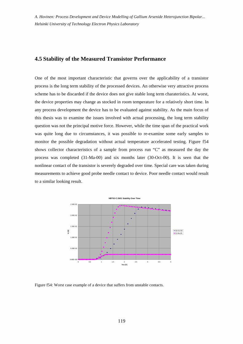
A. Hovinen: Process Development and Device Modelling of Gallium Arsenide Heterojunction Bipolar...
Helsinki University of Technology Electron Physics Laboratory
119
4.5 Stability of the Measured Transistor Performance
One of the most important characteristic that governs over the applicability of a transistor
process is the long term stability of the processed devices. An otherwise very attractive process
scheme has to be discarded if the device does not give stable long term charateristics. At worst,
the device properties may change as stocked in room temperature for a relatively short time. In
any process development the device has to be evaluated against stability. As the main focus of
this thesis was to examine the issues involved with actual processing, the long term stability
question was not the principal motive force. However, while the time span of the practical work
was quite long due to circumstances, it was possible to re-examine some early samples to
monitor the possible degradation without actual temperature accelerated testing. Figure f54
shows collector characteristics of a sample from process run “C” as measured the day the
process was completed (31-Ma-00) and six months later (30-Oct-00). It is seen that the
nonlinear contact of the transistor is severely degraded over time. Special care was taken during
measurements to achieve good probe needle contact to device. Poor needle contact would result
to a similar looking result.
Figure f54: Worst case example of a device that suffers from unstable contacts.
HBT02-C:2601 Stability Over Time
0.00E+00
5.00E-03
1.00E-02
1.50E-02
2.00E-02
2.50E-02
0 0.5 1 1.5 2 2.5 3 3.5 4
Vce [V]
Ic [
A] 30-Oct-00
31-Ma-00

A. Hovinen: Process Development and Device Modelling of Gallium Arsenide Heterojunction Bipolar...
Helsinki University of Technology Electron Physics Laboratory
120
The instability is understandable with reference to the process diary of the sample. During the
processing of sample C the surface preparation prior to metal depositions may have been
inadequate. The lift-off lithography was not finalised by oxygen plasma removal of resist
residuals because of the wish to avoid heating effect from the plasma reactor. Lithography was
finalized only by rinsing in deionised water for a predetermined time to dilute out the residual
developer from the sample, followed by NH4OH and HCl dips prior to metallisation.
It is very probable that not all of the residual developer or resist was removed. As a result, the
sample surface was probably not clean enough for a high quality contact formation.
Additionally, the evaporation of ohmic metals for emitter and collector were far from succesfull
according to process diary. From Figure f54 it is also seen that the current gain of the device
was not affected by ageing, which suggests that the actual epitaxial composition of the device
did not alter over time.
Figure f55 shows how the stress introduced by device measurements may affect the degraded
contacts. A transistor from the process run “C” that had degraded for six months showing
similar symptoms as in Figure f54 was stressed by repeated measurement sweeps for collector
characteristics. The 4145 parameter analyzer with “medium” integration time was used in the
experiment. One measurement sweep completed in about 10 seconds. Special care was taken to
achieve good probe needle contacts to device.
The measurement was left running in a loop for definite time to monitor possible changes.
Figure f55 gives collector characteristics of the device at the beginning of the experiment (blue
diamonds), after one hour (pink squares) and after 20 hours (yellow triangles). It is seen from
the figure that the repeated measurement stress affected both the contact region and current
gain of the device. Most of the change occurred within 1 hours. The 20 hours result diverges
from 1 hour result in high current region mainly due to probe needle contact degradation.
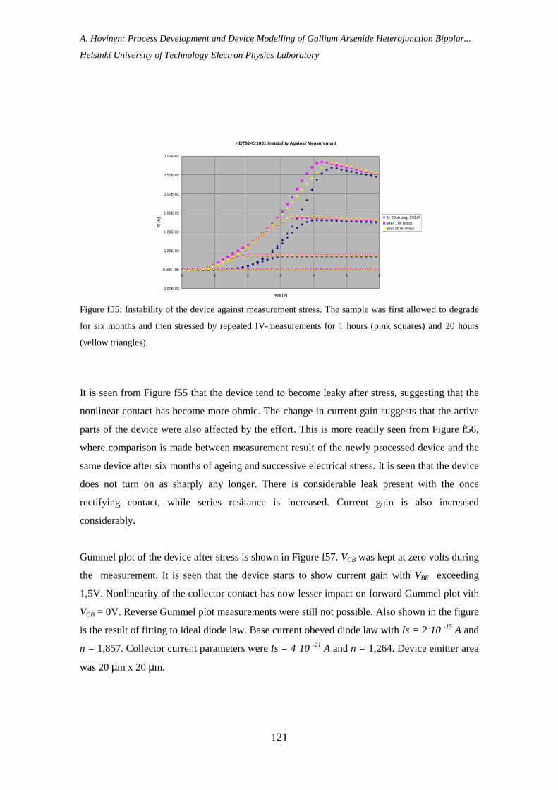
A. Hovinen: Process Development and Device Modelling of Gallium Arsenide Heterojunction Bipolar...
Helsinki University of Technology Electron Physics Laboratory
121
Figure f55: Instability of the device against measurement stress. The sample was first allowed to degrade
for six months and then stressed by repeated IV-measurements for 1 hours (pink squares) and 20 hours
(yellow triangles).
It is seen from Figure f55 that the device tend to become leaky after stress, suggesting that the
nonlinear contact has become more ohmic. The change in current gain suggests that the active
parts of the device were also affected by the effort. This is more readily seen from Figure f56,
where comparison is made between measurement result of the newly processed device and the
same device after six months of ageing and successive electrical stress. It is seen that the device
does not turn on as sharply any longer. There is considerable leak present with the once
rectifying contact, while series resitance is increased. Current gain is also increased
considerably.
Gummel plot of the device after stress is shown in Figure f57. VCB was kept at zero volts during
the measurement. It is seen that the device starts to show current gain with VBE exceeding
1,5V. Nonlinearity of the collector contact has now lesser impact on forward Gummel plot vith
VCB = 0V. Reverse Gummel plot measurements were still not possible. Also shown in the figure
is the result of fitting to ideal diode law. Base current obeyed diode law with Is = 2 .10 -15 A and
n = 1,857. Collector current parameters were Is = 4 .10 -21 A and n = 1,264. Device emitter area
was 20 µm x 20 µm.
HBT02-C:1001 Instability Against Measurement
-5.00E-03
0.00E+00
5.00E-03
1.00E-02
1.50E-02
2.00E-02
2.50E-02
3.00E-02
0 1 2 3 4 5 6
Vce [V]
IC [
A] Ib: 50uA:step 250uA
after 1 hr stress
after 20 hr stress

A. Hovinen: Process Development and Device Modelling of Gallium Arsenide Heterojunction Bipolar...
Helsinki University of Technology Electron Physics Laboratory
122
Figure f56: Device characteristics after six months of ageing and electrical stress.
Figure f57: Gummel plot of the device after stress experiment.
HBT02-C:1001 Gummel Plots After Electrical Stress. (Vcb = 0V)
y = 2E-15e20.833x
y = 4E-21e30.608x
1E-13
1E-12
1E-11
1E-10
1E-09
1E-08
1E-07
1E-06
1E-05
0.0001
0.001
0.01
0.1
1
-0.5 0 0.5 1 1.5 2 2.5 3
Vbe [V]
Ic, I
b [
A]
Ic
Ib
Ic fit
Ib fit
Expon. (Ib fit)
Expon. (Ic fit)
HBT02-C:1001 Collector Characteristics: As processed result versus aged and electrically stressed result
-5.00E-04
0.00E+00
5.00E-04
1.00E-03
1.50E-03
2.00E-03
-1 -0.5 0 0.5 1 1.5 2 2.5 3 3.5 4
Vce [V]
Ic [
A]
Ib = 0 uA
Ib = 50 uA
Ib = 100 uA
Ib = 150 uA
Ib = 200 uA
afte 7 months & reviving

A. Hovinen: Process Development and Device Modelling of Gallium Arsenide Heterojunction Bipolar...
Helsinki University of Technology Electron Physics Laboratory
123
( ) .ln eCebBs
BBE RIRRI
I
I
q
nkTV +++
=
It is worth to note that transistor measurements with forced base current implicitly force VBE to
vary accordingly in order to maintain constant base current over the entire sweep of VCE. Figure
f58 shows the VBE variation as observed during the measurements for Figure f56. IB values with
dotted labels refer to the measurement after ageing and electrical stress. It is seen that external
base voltage for a given base current was increased considerably, and VBE for low VCE values is
no longer constant because of the leak currents. In that respect, the as-processed measurement
result is pathologically neat, suggesting that the VBE result may be interpreted with simple
arguments. Considering VBE being affected by resistive loss across base resitance Rb and emitter
resistance Re , and emitter diode obeying diode law, and assuming that all of the base current
eventually flow through emitter resistance, VBE should be calculated by
(e137)
Figure f58: VBE that was needed to maintain the constant base current condition during measurements for
Figure f56.
HBT02-C:1001 Comparison of Vbe during IV measurement.
0.7
0.9
1.1
1.3
1.5
1.7
1.9
2.1
-0.5 0 0.5 1 1.5 2 2.5 3 3.5 4
Vce [V]
Vbe [V
Ib=50 uA
Ib =100 uA
Ib = 150 uA
Ib = 200 uA
Ib' = 50 uA
Ib' = 100 uA
Ib' = 150 uA
Ib' = 200 uA

A. Hovinen: Process Development and Device Modelling of Gallium Arsenide Heterojunction Bipolar...
Helsinki University of Technology Electron Physics Laboratory
124
Trial to fit the as-processed measurement data into equation (e137) was not satisfactory unless
the emitter resistance value was allowed to drift. Equation (e137) fitted to measurement data
with diode ideality factor n = 2 and Rb = 50 Ω when Re and Is depended on base current as
shown in Table IV. It is seen that the heterojunction emitter had a nonlinear character left
despite the compositional grading of the epitaxial structure of the device, which is reflected into
the necessity to vary the value of Re in the simple fitting equation of the as-processed device.
The stress experiment may have affected the device emitter heterojunction in a way that the
residual conduction band spike was lowered while the ohmic losses in the emitter volume
increased yielding to the observed results of Figure f56 for gain and turn on characteristics. In
normal operation at junction temperatures below 2500C HBTs are known to degrade by
increase in the number of point defects with a current assisted mechanism [r50], [r54], [r55].
Rapid degradation was associated with a dark line defect that was identified with
electroluminescence imaging method.
It may be concluded that the emitter heterojunction design need to be re-evaluated for future
applications. One of the weakest design parameters was the thickness of spacer layer that was
to prevent Be diffusion into emitter heterojunction, which should have been determined
experimentally. Also, the grading distances in either side of the emitter may not have been at
optimum. It seems that the observed high numerical values of emitter resistances were only
partially due to ohmic contacts, and the possibility of the existence of the conduction band
spike has to be taken into account in the Spice simulations. For the devices processed within
this thesis the series resistances were themselves high, such that the device DC performance
was possible to be modeled through a simple pSpice transistor equivalent circuit as the finer
aspects of heterojunction were screened out.
Ib = 50 µA Ib = 100 µA Ib = 150 µA Ib = 200 µA
Is 8.10–15 A 4.10–15 A 3.10–15 A 2.10–15 A
Re 950 Ω 400 Ω 250 Ω 150 Ω
TABLE IV: Saturation current and emitter resistance as obtained from VBE fit to measurement data of the
as-processed device.

A. Hovinen: Process Development and Device Modelling of Gallium Arsenide Heterojunction Bipolar...
Helsinki University of Technology Electron Physics Laboratory
125
4.6 Evaluation of the Frequency Response of the Processed Devices
The purpose of this thesis was to study the processing of new semiconductor devices such as
heterojunction bipolar transistors. Optimisation for high speed device performance is relevant
as soon as the processing itself is at routine level. This thesis contained just about enough
process runs to set up the minimum level of practise for routine processing of conventional
mesa isolated heterojunction devices for DC and low frequency purposes. It was beyond the
scope of this thesis to raise up a process flow that could be directly applied to high volume
production of commercially relevant devices. The optimisation for high speed is about
minimising parasitic resistances and reactances in device design to minimise RC delays in the
circuit. Matching the device to the signal line is crucial beyond frequencies over a few
gigahertz. It would not have been practical to jump over to high speed optimisation with this
thesis, due to the lack of previous knowledge on process parameters. The high speed
performance of the processed devices was thus of secondary importance.
However, as a demonstration of the capabilities of heterojunction bipolar technology, frequency
characteristics of a device from process run “B” was measured for future reference. The device
emitter area was 10 µm x 50 µm with sigle sided base contact. The original device was of DC
design with measurement pads in a conventional 100 µm x 100 µm matrix. The device wiring
metallisation was redesigned and reprocessed to facilitate on-wafer RF-probing with G-S-G
type probes in 150 µm pitch. As a useful addendum to the processing skills in the laboratory, a
simple electron beam process was set up for lithographical mask making, and the device wiring
metallisation was reprocessed by add-on method to adopt G-S-G probing.
Scattering parameter measurement was performed by Microwave Engineering Laboratory of
Technical University of Berlin. The bias condition was VCE = 6,0V and VBE = 1,7 V for IC = 12
mA and IB = 650 µA in common emitter configuration. Frequency was swept from 100MHz to
6900MHz during S-parameter measurement. Scattering parameter S21 gives the forward
transfer characteristics from base-emitter input port to collector-emitter output port. Small
signal current gain of the device is obtained after converting scattering parameters to hybrid or
h-parameters. The magnitude of parameter h21 gives device current gain. There are several
tools available for doing the mechanical conversion automatically.

A. Hovinen: Process Development and Device Modelling of Gallium Arsenide Heterojunction Bipolar...
Helsinki University of Technology Electron Physics Laboratory
126
For this thesis the conversion was done with a demonstration version of Smith -software
programmed in University of Applied Sciences, Berne, Switzerland, and distributed at the time
of writing as freeware by RFGlobalnet at www.rfglobalnet.com site. Figure f59 shows the
frequency dependence of the small signal gain for the measured device. The current gain cuts
off at ft = 2,3 GHz. According to data analysis with Smith-software the maximum oscillation
frequency fmax, or the maximum power gain cut off frequency, was about 1,1 GHz. In a well
designed HBT the current gain rolls off at a rate of 20 dB per decade increase of frequency.
Tenfold increase in frequency should reduce gain tenfold. In Figure f59 the decrease is only
fourfold, or 12 dB/decade. It is known that excessive back injection current in base-emitter
junction causes the slope to reduce to 10dB/decade [r14]. The explanation is adequate for the
transistor under measurement, and is an indication that the valence band discontinuity was not
holding off holes efficiently at the used bias conditions for measurement.
It may be concluded that even the basic process that was designed for DC device
characterisation with apparent emitter resistances of about hundred times more than preferable
was capable of introducing power gain in gigahertz range. This is an encouraging result for the
future refinement of the process towards applicable high speed device processing.
Figure f59: Small signal gain versus frequency of the measured transistor. The current gain cut off
frequency was ft = 2,3 GHz.
HBT02-B:1402 Current Gain versus frequency
0.1
1
10
100 1000 10000
Frequency [MHz]
Cu
rren
t G
ain
(|h
21|)
A. Hovinen: Process Development and Device Modelling of Gallium Arsenide Heterojunction Bipolar...
Helsinki University of Technology Electron Physics Laboratory
127
5 Conclusions
Processing and characterization of high speed compound semiconductor devices was studied
with emphasis on the conventional wet chemically isolated AlGaAs/GaAs heterojunction
bipolar transistor. The aim was to develop a laboratory scale process for research and
educational purposes. Physical one dimensional device simulation and practical work on
process development together resulted in a feasible process scheme. Excluding the numerous
separate experiments on the individual process steps, the process development contained three
complete process runs. The current gain and DC performance of the last processed samples
accorded with the simulation predictions showing that the process is applicable to reach
controlled device performance. The measurement results were possible to fit into a simple
pSpice equivalent circuit with appreciable confidence.
At early stage of process development it was observed that the first devices were easily
destroyed by excessive heating during ohmic contact formation. The process was then modified
towards low thermal energy budget, avoiding any source of heat but implicit to the PECVD
nitridation. Different contact metal choices were tested for applicability in non-alloyed contact
formation against a reference of a Cr/Au based non-alloyed scheme. It was verified that for
short term testing purposes Cr/Au may serve as a basic contact metal if InGaAs-capped emitter
is used. Collector contact will then be a rectifying diode. Substitution of Cr/Au with
Pd/Ge/Pd/Au resulted in ohmic contacts in both emitter and collector. It was also observed that
a device with Pd/AuGe/Ag/Au with InGaAs capping layer as emitter contact scheme, Ni/AuZn
as base contact scheme and Cr/Au rectifying collector diode contact yielded to very good
transistor performance with respect to DC characteristics. However, it was left open whether
the actual collector contact contained residuals of palladium, which is a true possibility with
reference to the process diary. Palladium is known on its capability to penetrate native oxides,
which may have helped in collector contact formation. Future refinement of the process should
include re-examination of the collector metallisation comparing Cr/Au and Pd/Cr/Au. Finally, it
was observed that the processed devices were rather unstable with time and with electrical
stress. This is conceivable to occur with low thermal budget processing. The long term
reliability is a concern if the process if further refined towards device applications.
A. Hovinen: Process Development and Device Modelling of Gallium Arsenide Heterojunction Bipolar...
Helsinki University of Technology Electron Physics Laboratory
128
Shallow air bridges and metal cross-overs were included to facilitate process application for
the future needs in high speed compound semiconductor device processing. Passive structures
such as coils, capacitors and resistors are possible with the process. Electrochemical plating of
wiring metallization should be further examined to turn the process more applicable with
respect to low resistivity wiring and mechanically stronger air bridging. Preliminary tests on
copper plating were made, but not included in the text of this thesis in length. The tests showed
that the plating process should not possess a problem, if the adhesion of initial wiring metal is
good enough. Otherwise the plated metal contains bumps of loose metal film. A perhaps useful
note for future reference about the plating experiment was that also the back side of the GaAs
wafer got plated by copper during the experiment seemingly smoothly. This should facilitate
the process refinement towards high speed devices with ground metallizations carried through
via holes in the thinned GaAs substrate.
Although the processing steps were demonstrated with AlGaAs/GaAs-based material, most of
the processing methods that were adopted are applicable also for, e.g., GaInAs/InP-material
with some adjustment in etching processes and metallisation choices. As such, the process is
ready to be used as a tool for laboratory scale research and education on HBT technology.

A. Hovinen: Process Development and Device Modelling of Gallium Arsenide Heterojunction Bipolar...
Helsinki University of Technology Electron Physics Laboratory
129
6 Acknowledgements
I wish to thank Dr. Alexei Malinin and Janne Kylmäluoma for assistance with PECVD
nitrides, and Dr. Anni Seppälä from Helsinki University for the Rutherford back scattering
measurements during the studies of e-beam evaporated metal layers. The staff with the
Laboratory of Electronics Production Technology of Helsinki University of Technology was of
great help in the plating experiments and with the interpretation of phase diagrams of metal
compounds. Dr. Mikko Taskinen and Dr. Lauri Knuuttila deserve a special thank for making
my early HBT samples with Zn-base doping with their MOCVD at Optoelectronics laboratory
of Helsinki University of Technology. I appreciate the contribution of EMCEC Oy to this work
by donation of the HP4145A parameter measurement apparatus with associated fixtures for
Electron Physics Laboratory.
I express my gratitude to Dr. Darrell Hill with TriQuint Semiconductor for his warm
encouragement and sympathy during my early efforts in process development of HBT’s. I also
express my appreciation to Dr. Nikolai Maleev with A. F. Ioffe Physico-Technical
Institute, St. Petersburg, for his fruitful comments on the design of the epitaxial structure of the
HBT and growing the final samples with beryllium base doping with their MBE. I wish also to
acknowledge the help of Dr. Kai Schmidt von Behren with Microwave Engineering Laboratory
of Technical University of Berlin, with the scattering parameter measurements of the
transistors. Most of all, I wish to hail the contribution of Mr. Risto Salo to my work by his
uncompromising devotion to the cause of modernisation of the clean room facilities in our
university.

A. Hovinen: Process Development and Device Modelling of Gallium Arsenide Heterojunction Bipolar...
Helsinki University of Technology Electron Physics Laboratory
130
7 References
[r01] Kroemer H: Heterostructure Bipolar Transistors and Integrated Circuits, Proc. IEEE,
Vol. 70, No. 1, 1982, pp. 13-25
[r02] The Royal Academy of Sciences Press Release on the Nobel Prize in Physics 2000,
October 10, 2000
[r03] Kroemer, H.: Theory of a Wide-Gap Emitter for Transistors, Proc. IRE, Vol. 45, No.
11, 1957, pp. 1535-1537
[r04] Morozov, Y. V.: Personalia Zhores Ivanovich Alferov (on his seventieth birthday),
Physics – Uspekhi, Vol. 43, no. 3, 2000, pp. 307-08
[r05] U.S. Patent No. 2569347 to W. Shockley, Filed 26 June 1948, expired 24 September
1968
[r06] Bardeen J., Brattain W. H.: The Transistor, a Semi-Conducting Triode, Phys. Rev.,
Vol. 74, June 25, 1948, pp. 230-331
[r07] Hill, D.: High Voltage HBT Technology, IEEE 20th GaAs IC Symposium 1998
Technical digest, 1998, pp. 149 - 52
[r08] Lee, Q., Martin, S. C., Mensa, D., Smith, R. P., Guthrie, J., Rodwell, M. J. W.:
Submicron Transferred-Substrate Heterojunction Bipolar Transistors, IEEE Eletron.
Dev. Lett., Vol. 20, No. 8, 1999 pp. 396-98
[r09] Hovinen, A.: Fabrication of a Heterojunction Transistor, Master’s Thesis, Electron
Physics Laboratory, Helsinki University of Technology, Espoo 1992 (in Finnish)
[r10] Hovinen A.: Fabrication of a Crystalline Thin Film Solar Cell, Licentiate’s Thesis,
Electron Physics Laboratory, Helsinki University of Technology, Espoo 1995 (in
Finnish)
[r11] Anholt R., Electrical and Thermal Characterization of MESFETs, HEMTs, and HBTs, ,
Artech House, Boston, 1995
[r12] Seely, S.: Electron Tube Circuits, McGraw-Hill, N.Y., 1958
[r13] Sze, S. M., Physics of Semiconductor Devices, 2nd ed., John Wiley & Sons, New York,
1981
[r14] Liu, W., Handbook of III-V Heterojunction Bipolar Transistors, John Wiley & Sons,
New York, 1998
[r15] Wood, D.: Optoelectronic Semiconductor Devices, Prentice Hall, Hertfordshire, 1994
A. Hovinen: Process Development and Device Modelling of Gallium Arsenide Heterojunction Bipolar...
Helsinki University of Technology Electron Physics Laboratory
131
[r16] Das, M. B. in Ali, F., Gupta, A.: HEMTs and HBTs : Devices, Fabrication, and
Circuits, Artech House, Boston (MA), 1991
[r17] Böer, K.W., Survey of Semiconductor Physics, Vol II: Barriers, Junctions, Surfaces
and Devices, Van Nostrand Reinhold, New York, 1992
[r18] Alonso, M., Finn, E. J.: Fundamental University Physics, Vol 1: Mechanics and
Thermodynamics, 2nd ed., Addison-Wesley, 1980
[r19] Grinberg, A. A., Shur, M. S., Fischer, R. J., Morkoc, H.: An Investigation of the Effect
of Graded Layers and Tunneling on the Performance of AlGaAs / GaAs Heterojunction
Bipolar Transistors, IEEE Trans. El. Dev., vol. ED-31, no. 12, December 1984
[r20] Das, A., Lundstrom, M. S., Numerical Study of Emitter-Base Junction Design for
AlGaAs/GaAs Heterojunction Bipolar Transistors, IEEE Trans. El. Dev., vol. 35, no. 7,
July 1988
[r21] Kennedy, D. P.: The Potential and Electric Field at the Metallurgical Boundary of an
abrupt p-n semiconductor junction, IEEE Trans. Electr. Dev., 22, 1975, 988-994
[r22] Basore P. A. et al.: PC-1D Version 2: Enhanced Numerical Solar Cell Modeling,
Proceedings of the 20th IEEE Photovoltaic Specialists Conference, pp. 389-96, 1988
[r23] Shur, M.: Recombination Current in Forward Biased p-n junctions, IEEE Trans. El.
Dev., vol. 35, no. 9, September 1988
[r24] Klausmeier-Brown, M. E., Lundstrom, M. S., Melloch, M. R.: The effects of Heavy
Impurity Doping on AlGaAs/GaAs Bipolar Transistors, IEEE Trans. El. Dev., Vol. 36,
no. 10, 1989
[r25] Harmon, E. S., Melloch, M. R., Lundstrom, M. S.: Effective Band Gap Shrinkage in
GaAs, Appl. Phys. Lett., Vol. 64, no. 4, 1994
[r26] Hovinen, A., Malinin, A., Lipsanen A.: Lithography in Experimental Environment,
Reports in Electron Physics 2000/21, Helsinki University of Technology, Espoo 2000
[r27] Hovinen, A., Lipsanen A.: Processing of AlGaAs-GaAs Heterojunction Bipolar
Transistors, Reports in Electron Physics 2000/22, Helsinki University of Technology,
Espoo 2000
[r28] Kurishima, K. et al., Growth, Design and Performance of InP-based Heterostructure
Bipolar Transistors, K. IEICE Trans. Electron., vol. E78-C, no. 9, pp. 1171-80, 1995
[r29] Shur, M., GaAs Devices and Circuits, M. Plenum Press, New York, 1987
[r30] Tiwari, S., Wright, S.L., Frank, D. J.: Compound Semiconductor Heterostructure
Bipolar Transistors, IBM J. Res. Develop. vol. 34, no. 4, 1990

A. Hovinen: Process Development and Device Modelling of Gallium Arsenide Heterojunction Bipolar...
Helsinki University of Technology Electron Physics Laboratory
132
[r31] Wang, L. C., Wang, X. Z., Lau, S. S., Sands, T., Chan, W. K., Kuech, T. F.: Stable
and Shallow PdIn ohmic Contacts to n-GaAs, Appl. Phys. Lett., vol 56, no. 21, pp.
2129-31, 1990
[r32] Pruniaux, B. R., Adams, A. C.: Dependence of Barrier Height of Metal Semiconductor
(Au-GaAs) on Thickness of Semiconductor Surface Layers, J. Appl. Phys., vol. 43, pp.
1980-03, 1972
[r33] Mukherjee, S. D., Woodard, D. W.: Etching and Surface Preparation of GaAs for
Device Fabrication, in Howes, M. J., Morgan D. V. (ed.): Gallium Arsenide Materials,
Devices and Circuits, New York, 1985, John Wiley & Sons, pp. 119-60
[r34] Shih, Y.-C., Murakami, M., Wilkie, E. L., Callegari A. C.: Effects of Interfacial
Microstructure on Uniformity and Thermal Stability of AuNiGe Ohmic Contact to N-
type GaAs, J. Appl. Phys., vol 62, no. 2, pp. 582-9, 1987
[r35] Stareev, G., Künzel, H.: A Controllable Mechanism of Forming Extremely Low-
resistance Nonalloyed Ohmic Contacts to Group III-V Compound Semiconductors, J.
Appl. Phys., vol. 74, no. 12, pp. 7344-56, 1993
[r36] Yeh, Y.-H., Lai, J.-T., Lee, J. Y.: Low Contact–Resistance and Shallow Pd/Ge Ohmic
Contacts to n- In0.53Ga0.47As on InP Substrate Formed by Rapid Thermal Annealing,
Jpn. J. Appl. Phys., vol. 35, pp. L 1569-71, 1996
[r37] Huelsman, A. D., Fonstad, C. G.: Compositional Changes during Alloying of Ohmic
Contacts to In0.53Ga0.47As, J. Electrochem. Soc. Solid-State Science and Technology,
vol. 132, no. 12, pp. 2989-92, 1985
[r38] Wakita, A., Moll, N., Ficher-Colbrie, A.: Design and Surface Chemistry of Nonalloyed
Ohmic Contacts to Pseudomorphic InGaAs on n+GaAs, J. Appl. Phys., vol. 68, no. 6,
pp. 2833-8, 1990
[r39] Massalski, T.B.: Binary Alloy Phase Diagrams, ASM International, 1996
[r40] Stareev, G.: Formation of Extremely low Resistance Ti/Pt/Au ohmic Contacts to p-
GaAs, Appl. Phys. Lett. vol. 62, no. 22, pp. 2801-03, 1993
[r41] Sugiyama T. et al..: Ultra-Low Resistance Base Ohmic Contact with Pt/Ti/Pt/Au for
High-fmax AlGaAs / GaAs Heterojunction Bipolar Transistors, Jpn. J. Appl. Phys., vol.
33. part 1, no. 1B, pp. 786-9, 1994
[r42] Kazuhiko, T., Masaru, S., Koichi, K.: Submicrometer Optical Lithography Using a
Double-Layer Resist by a single Development Technology, IEEE Trans. on El. Dev.,
vol. ED-31, no. 12, 1984
A. Hovinen: Process Development and Device Modelling of Gallium Arsenide Heterojunction Bipolar...
Helsinki University of Technology Electron Physics Laboratory
133
[r43] Liou, Juin J., Huang, Chern I., Bayraktaroglu, B.: A Physics Based, Analytical
Heterojunction Bipolar Transistor Model Including Thermal and High Current Effects,
IEEE Trans. El. Dev., Vol. 40, no. 9, 1993
[r44] Suematsu, E., Ogawa, H.: Frequency Response of HBT’s as Photodetectors, IEEE
Microwave and Guided Wave Letters, Vol. 3., no. 7, 1993
[r45] Blakemore, J. S.: Semiconducting and Other Major Properties of Gallium Arsenide, J.
Appl. Phys., vol 53, no. 10, 1982
[r46] Sinkkonen, J., Ruokolainen J., Uotila P., Hovinen A.: Spatial Collection Efficiency of a
Solar Cell, Appl. Phys. Lett., vol. 66., no. 2, 1995
[r47] Roenker, K. P., Frimel, S. M., Cahay, M. M.: Effects of Optical Absorption on the
Quasi Fermi Level Splitting at the Emitter-Base Junction in npn Heterojunction
Bipolar Phototransistors, IEEE Trans. El. Dev., Vol. 46., no. 4, 1999
[r48] Grove, A.S.: Physics and Technology of Semiconductor Devices, J. Wiley & Sons, New
York, 1967
[r49] Hovinen, A.: Fitting of the Solar Cell IV-curve to the Two Diode Model, Physica
Scripta, Vol. T54, 1994 pp. 175 – 76
[r50] Henderson, T.: Model for Degradation of GaAs/AlGaAs HBTs Under Temperature and
Current Stress, 1995 IEEE International Electron Devices Meeting Digest, pp. 811-14
[r51] Das, M. B. in Ali, F., Gupta, A.: HEMTs and HBTs : Devices, Fabrication and
Circuits, Artech House, Boston, 1991
[r52] Morkoc, H, Sverdlov, B., Gao, Guang-Bo: Strained Layer Heterostructures and their
Applications to MODFET’s, HBT’s and Lasers, Proc. IEEE, vol. 81, no. 4, 1993, pp.
493 – 56
[r53] Nagata, K. et al.: Self-aligned AlGaAs/GaAs HBT with Low Emitter Resistance
Utilizing InGaAs Cap Layer, IEEE Trans. El. Dev., vol. ED-35, no. 1, 1988, pp.2-7
[r54] Bovolon, N., et al.: Analysis of the Short-Term DC-Current Gain Variation During
High Current Density-Low Temperature Stress of AlGaAs/GaAs Heterojunction
Bipolar Transistors, IEEE Trans. El. Dev., vol. 47, no. 2, 2000, pp. 274 – 81
[r55] Adlerstein, M. G., Gering, J. M.: Current Induced Degradation in GaAs HBT’s, IEEE
Trans. El. Dev., vol. 47, no. 2, 2000, pp. 434 – 39
[r56] Marsh, S. P.: Direct ExtractionTechnique to Derive the Junction Temperature of HBT’s
Under High Self-Heating Bias Conditions, IEEE Trans. El. Dev., vol. 47, no. 2, 2000,
pp. 288 – 91
Related Documents