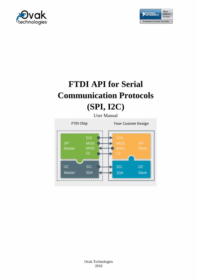
Ovak Technologies 2016 FTDI API for Serial Communication Protocols (SPI, I2C) User Manual

Welcome message from author
This document is posted to help you gain knowledge. Please leave a comment to let me know what you think about it! Share it to your friends and learn new things together.
Transcript
Ovak Technologies
2016
FTDI API for Serial
Communication Protocols
(SPI, I2C) User Manual
2
Contents 1. Introduction ................................................................................................................................... 4
1.1. Definitions and Acronyms ...................................................................................................... 4
1.2. The Purpose ............................................................................................................................ 4
1.3. Overview ................................................................................................................................. 4
2. Transfer Library and License Files to NI Linux Real-Time ..................................................... 5
3. How to use FTDI API for Serial Communication Protocols ..................................................... 5
3.1. Open.vi .................................................................................................................................... 6
3.2. Write-Read.vi .......................................................................................................................... 7
3.3. Close.vi ................................................................................................................................... 8
3.4. D2XX Driver .......................................................................................................................... 8
4. FT4222H Programming Interface (API) ................................................................................ 9
4.1. FT4222 General Functions...................................................................................................... 9
4.1.1. Open and Close ............................................................................................................... 9
4.1.2. Un-initialize .................................................................................................................... 9
4.1.3. Set Clock ......................................................................................................................... 9
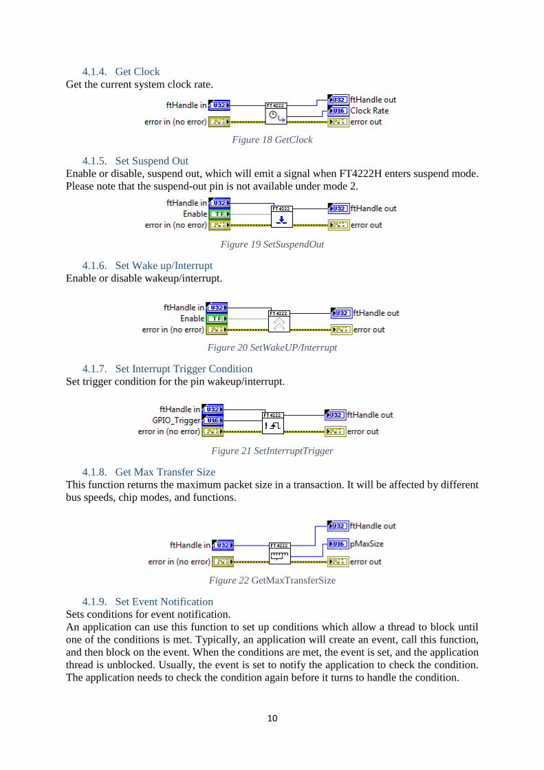
4.1.4. Get Clock ...................................................................................................................... 10
4.1.5. Set Suspend Out ............................................................................................................ 10
4.1.6. Set Wake up/Interrupt ................................................................................................... 10
4.1.7. Set Interrupt Trigger Condition ..................................................................................... 10
4.1.8. Get Max Transfer Size .................................................................................................. 10
4.1.9. Set Event Notification ................................................................................................... 10
4.2. SPI Master Functions ............................................................................................................ 11
4.2.1. SPI Master Init .................................................................................................................. 11
4.2.2. SPI Master Set Lines ......................................................................................................... 12
4.2.3. SPI Master Single Read .................................................................................................... 12
4.2.4. SPI Master Single Write ................................................................................................... 12
4.2.5. SPI Master Single Read and Write.................................................................................... 12
4.2.6. SPI Master Multi Read and Write ..................................................................................... 13
4.3. SPI Slave Functions .............................................................................................................. 13
4.3.1. SPI Slave Init ................................................................................................................ 13
4.3.2. SPI Slave Get Rx Status ................................................................................................ 13
4.3.3. SPI Slave Read .............................................................................................................. 14
4.3.4. SPI Slave Write ............................................................................................................. 14
4.4. SPI General Functions .......................................................................................................... 14
4.4.1. SPI Reset Transaction ....................................................................................................... 14
4.4.2. SPI Reset ........................................................................................................................... 14
4.4.3. SPI Set Driving Strength ................................................................................................... 14

3
4.5. I2C Master Functions ............................................................................................................ 15
4.5.1. I2C Master Init .............................................................................................................. 15
4.5.2. I2C Master Read ........................................................................................................... 15
4.5.3. I2C Master Write .......................................................................................................... 15
4.5.4. I2C Master Write Extension ......................................................................................... 15
4.5.5. I2C Master Read Extension .......................................................................................... 16
4.5.6. I2C Master GetStatus .................................................................................................... 16
4.5.7. I2C Master Reset ........................................................................................................... 16
4.6. I2C Slave Functions .............................................................................................................. 16
4.6.1. I2C Slave Init ................................................................................................................ 16
4.6.2. I2C Slave Get Address .................................................................................................. 16
4.6.3. I2C Slave Set Address................................................................................................... 17
4.6.4. I2C Slave Get Rx Status ................................................................................................ 17
4.6.5. I2C Slave Read.............................................................................................................. 17
4.6.6. I2C Slave Write ............................................................................................................. 17
4.6.7. I2C Slave Reset ............................................................................................................. 17
4.7. GPIO Functions .................................................................................................................... 18
4.7.1. GPIO Init ....................................................................................................................... 18
4.7.2. GPIO Read .................................................................................................................... 18
4.7.3. GPIO Write ................................................................................................................... 18
4.7.4. GPIO Set Input Trigger ................................................................................................. 19
4.7.5. GPIO Get Trigger Status ............................................................................................... 19
4.7.6. GPIO Read Trigger Queue ............................................................................................ 19
5. Examples ...................................................................................................................................... 19
5.1. SPI – Single Slave Example.................................................................................................. 19
5.2. SPI – Multiple Slaves Example Circuit ................................................................................ 20
5.3. FT4222 SPI Master Example ................................................................................................ 21
5.4. FT4222 SPI Slave Example .................................................................................................. 22
5.5. I2C – Single Slave Example Circuit ..................................................................................... 22
5.6. I2C – Multiple Slaves ........................................................................................................... 23
5.7. FT4222 I2C Master Example ................................................................................................ 23
5.8. FT4222 I2C Slave Example .................................................................................................. 23
6. System Requirements ................................................................................................................. 24
7. Suggested connections................................................................................................................. 25
8. Support Information ................................................................................................................... 25

4
1. Introduction
1.1. Definitions and Acronyms MPSSE – Multi-Protocol Synchronous Serial Engine
RAM – Random-Access Memory
CS – Chip Select
GPIO – General-Purpose input/output
SPI – Serial Peripheral Interface
CLK – Clock Frequency
MOSI – Master Output, Slave Input
1.2. The Purpose
The purpose of this manual is to outline the basics in configuring the MPSSE for use
and demonstrate some of the available modes of operation.
1.3. Overview
This API provides high-level building blocks to communicate with FTDI Multi-
Protocol Synchronous Serial Engine based on D2XX and FT4222H drivers.
The API enables users to write applications and communicate with the FTDI Chip’s
I2C/SPI/JTAG/GPIO devices without needing to understand the low-level D2XX and FT4222
drivers and theirs command sets. MPSSE provides a flexible means of interfacing
synchronous serial devices to a USB port. Being “Multi-Protocol”, the MPSSE allows
communication with many different types of synchronous devices; the most popular are SPI
and I2C. Data formatting and clock synchronization can be configured in a variety of ways to
satisfy almost any requirement. In addition to the serial data pins, additional GPIO signals are
available. The API support Windows and NI Linux RT. The Linux version of LibFT4222 has
D2XX built-in.
The FT4222H supports 4 operation modes to allow various I2C/SPI devices to be connected to
USB bus. The attachable device configuration for each mode is listed below:
Mode 0 (2 USB interfaces):
SPI master, SPI slave, I2C master, or I2C slave device
• GPIO device
• Mode 1 (4 USB interfaces):
• SPI master connects up to 3 SPI slave devices
• GPIO device
• Mode 2 (4 USB interfaces):
• SPI master connects up to 4 SPI slave devices
• Mode 3 (1 USB interface):
• SPI master, SPI slave, I2C master, or I2C slave device
In mode 0 and 3 the connected device can be a SPI/I2C master or slave, depending on how an
application developer initializes the FT4222H chip. Mode 1 and mode 2 are designed to
connect to multiple SPI slave devices.
The FT4222H can be configured with up to 4 GPIO pins for user applications in mode 0 and
mode 1, but each pin is multiplexed with interrupt/suspend out/SPI slave select/I2C functions
as listed below:
• gpio0 / ss1o / scl
5
• gpio1 / ss2o / sda
• gpio2 / ss3o / suspend out
• gpio3 / wakeup/intr
If the FT4222H is initialized as I2C device, with pins as mentioned above, the pins of gpio0
and gpio1 will be switched to scl and sda, and cannot be used as GPIO.
The pin for gpio2 is by default configured as suspend out, and the pin for gpio3 is configured
as wakeup/intr. Only these configured GPIO pins can support GPIO read/set operation
through the corresponding endpoint.
2. Transfer Library and License Files to NI Linux Real-Time There are many ways of transferring .so and license files to NI Linux RT. For example SSH,
WebDAV and FileZilla.
The NI Linux Real-Time OS offers full Linux shell support so you can perform complex
administrative tasks to manage real-time targets more easily. To access the shell, you need a
terminal client. If you use Windows 7 and later, then PuTTY is a popular and free client.
In addition to a terminal client, you must select the Enable Secure Shell Server (sshd) option
on the real-time target running the NI Linux Real-Time OS. You can use NI Measurement &
Automation Explorer (MAX).
NI real-time targets support WebDAV file transfer. WebDAV is an industry-standard protocol
that is based on top of HTTP. You can easily secure it to transfer libFT4222.so and
FTDI_license.ini files. WebDAV is the default file transfer mechanism for real-time targets
running NI Linux Real-Time.
After installing package you can find the libFT4222.so library in C:\Program Files
(x86)\National Instruments\LabVIEW 2013\vi.lib\Ovak Technologies\FTDI API for
LabVIEW\Supporting files path. We recommend to transfer these library and
FTDI_license.ini files to /usr/local/lib/ then reboot the controller. For deployment license you
need target's Serial Number.
3. How to use FTDI API for Serial Communication Protocols FTDI API is installed under “Instrument I/O” palette. The palette consists of high-level
MPSSE Polymorphic VIs “D2XX Drivers” and “FT4222H library” sub palette with low-
level VIs for D2XX and FT4222H driver call.
Figure 1 FTDI Driver API for Serial Communication Protocol (SPI, I2C)

6
3.1. Open.vi
Use “Open.vi” to configure the FTDI MPSSE for SPI I2C or JTAG protocols.
Just select Device ->Serial Protocol->Connection from Polymorphic drop-down menu.
Note: The MPSSE always acts as a master controller for the selected synchronous
interface.
Figure 2 FT2232H_SPI
Figure 3 Configure SPI.vi
This VI configures the FTDI MPSSE for SPI protocol. Sets the SPI CLK Frequency, SPI
Mode (only Mod0 and Mod2 are supported) and CS pins for slave device. The MPSSE can
be placed in loop-back mode for diagnostic purposes (data transmitted out of the DO pin,
is also internally connected to the DI pin).
Note: The MPSSE always acts as a master controller for the selected synchronous interface.
Figure 4 SPI - Multi Slaves.vi
This VI configures the FTDI MPSSE for SPI protocol. Sets the SPI CLK Frequency, SPI
Mode (only Mod0 and Mod2 are supported) and CS pins for slave devices. The MPSSE can
be placed in loop-back mode for diagnostic purposes (data is transmitted out of the DO pin,
is also internally connected to the DI pin).
This VI should be used when multiple slaves are connected to the bus.
Figure 5 Configure I2C.vi
This VI configures the FTDI MPSSE for I2C protocol. It sets the I2C CLK Frequency.
Registers the I2C Slave Device Address (7-bit address) interconnected to the bus.

7
Figure 6 Configure I2C - Multi Slaves.vi
This VI configures the FTDI Multi-Protocol Synchronous Serial Engine (MPSSE) for I2C
protocol. It sets the I2C CLK Frequency. Registers the I2C Slave Device Address (7-bit
address) interconnected to the bus.
This VI should be used when multiple slaves are connected to the bus.
3.2. Write-Read.vi
Performs Write/Read operations according to serial protocol you specify. The instances of
this polymorphic VI specify the data format to operate with, as well as a single or multiple
slaves are used on bus topology.
Figure 7 SPI_Single Slave
Figure 8 SPI_SingleSlave_ByteData.vi
This VI performs a full-duplex transfer of data with the slave device. In this case, data
("Write Data" bytes) is both sent to the slave and received from the slave at once.
Figure 9 SPI_MultipleSlaves_ByteData.vi
This VI performs a full-duplex transfer of data with the slave devices. In this action, data
("Write Data" bytes) is both sent to the slave and received from the slave at once.
This VI should be used when multiple slaves are connected to the bus.
Figure 10 SPI_MultipleSlaves_BitData.vi
This VI performs a full-duplex transfer of data with the slave devices. In this action, data
("Bit Data Out" bits) is both sent to the slave and received from the slave at once.
This VI should be used when multiple slaves are connected to the bus.
8
Figure 11 SPI_ SingleSlave_BitData.vi
This VI performs a full-duplex transfer of data with the slave device. In this action, data ("Bit
Data Out" bits) is both sent to the slave and received from the slave at once.
This VI should be used when multiple slaves are connected to the bus.
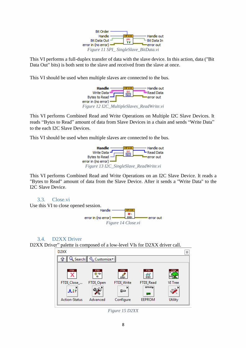
Figure 12 I2C_MultipleSlaves_ReadWrite.vi
This VI performs Combined Read and Write Operations on Multiple I2C Slave Devices. It
reads “Bytes to Read” amount of data from Slave Devices in a chain and sends “Write Data”
to the each I2C Slave Devices.
This VI should be used when multiple slaves are connected to the bus.
Figure 13 I2C_SingleSlave_ReadWrite.vi
This VI performs Combined Read and Write Operations on an I2C Slave Device. It reads a
"Bytes to Read" amount of data from the Slave Device. After it sends a "Write Data" to the
I2C Slave Device.
3.3. Close.vi Use this VI to close opened session.
Figure 14 Close.vi
3.4. D2XX Driver D2XX Driver” palette is composed of a low-level VIs for D2XX driver call.
Figure 15 D2XX

9
4. FT4222H Programming Interface (API) LibFT4222 supports SPI, I2C and GPIO communication using high-level APIs. In addition, it
provides chip configuration APIs, such as FT4222_SetClock.
After calling FT_Open, the FT4222H is required to be initialized by one of the following initial
functions:
• FT4222_SPIMaster_Init
• FT4222_SPISlave_Init
• FT4222_I2CMaster_Init
• FT4222_I2CSlave_Init
• FT4222_GPIO_Init
The initialization functions help developers to switch the FT4222H into a specific mode. At
the end of the application, FT4222_Uninitialize should be called to release allocated resources,
before calling FT_Close. All the APIs return FT4222_STATUS, which extends FT_STATUS
that is defined in the D2XX driver. FT4222_STATUS defines additional values to report
FT4222H specific status.
4.1. FT4222 General Functions The functions listed in this section are system-wise configuration functions.
4.1.1. Open and Close
An application of LibFT4222 should open the device and get a handle for subsequent accesses
by calling FT_Open or FT_OpenEx. Both are D2XX API. Please note that the FT4222H
assigns different functions to different interfaces. For example, under mode 0, interface A is
assigned as SPI or I2C interface, and interface B is assigned as GPIO interface.
After finishing using the device, FT_Close should be called to release the device.
4.1.2. Un-initialize
Release allocated resources. FT4222_Uninitialize should be called before calling FT_Close.
Figure 16 UnInitialize
4.1.3. Set Clock
Set the system clock rate. The FT4222H supports 4 clock rates: 80MHz, 60MHz, 48MHz, or
24MHz. By default, the FT4222H runs at 60MHz clock rate.
Figure 17 SetClock
10
4.1.4. Get Clock
Get the current system clock rate.
Figure 18 GetClock
4.1.5. Set Suspend Out
Enable or disable, suspend out, which will emit a signal when FT4222H enters suspend mode.
Please note that the suspend-out pin is not available under mode 2.
Figure 19 SetSuspendOut
4.1.6. Set Wake up/Interrupt
Enable or disable wakeup/interrupt.
Figure 20 SetWakeUP/Interrupt
4.1.7. Set Interrupt Trigger Condition
Set trigger condition for the pin wakeup/interrupt.
Figure 21 SetInterruptTrigger
4.1.8. Get Max Transfer Size
This function returns the maximum packet size in a transaction. It will be affected by different
bus speeds, chip modes, and functions.
Figure 22 GetMaxTransferSize
4.1.9. Set Event Notification
Sets conditions for event notification.
An application can use this function to set up conditions which allow a thread to block until
one of the conditions is met. Typically, an application will create an event, call this function,
and then block on the event. When the conditions are met, the event is set, and the application
thread is unblocked. Usually, the event is set to notify the application to check the condition.
The application needs to check the condition again before it turns to handle the condition.
11
Figure 23 SetEventNotification
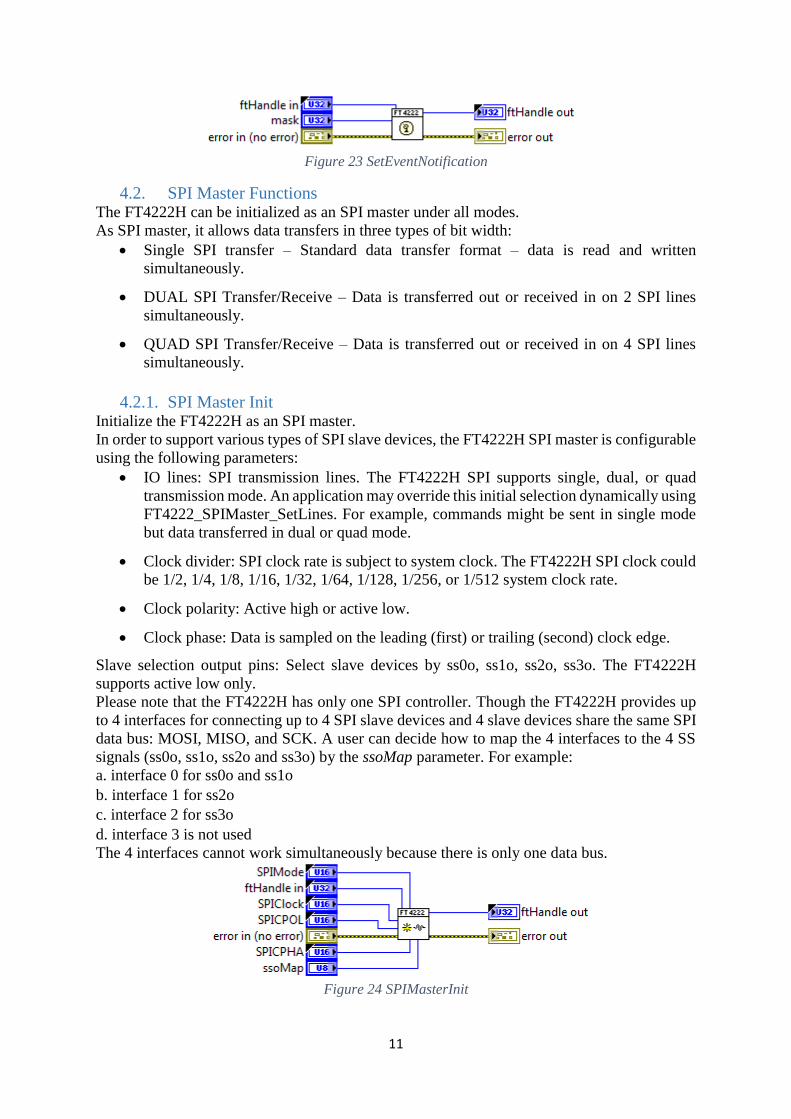
4.2. SPI Master Functions The FT4222H can be initialized as an SPI master under all modes.
As SPI master, it allows data transfers in three types of bit width:
• Single SPI transfer – Standard data transfer format – data is read and written
simultaneously.
• DUAL SPI Transfer/Receive – Data is transferred out or received in on 2 SPI lines
simultaneously.
• QUAD SPI Transfer/Receive – Data is transferred out or received in on 4 SPI lines
simultaneously.
4.2.1. SPI Master Init Initialize the FT4222H as an SPI master.
In order to support various types of SPI slave devices, the FT4222H SPI master is configurable
using the following parameters:
• IO lines: SPI transmission lines. The FT4222H SPI supports single, dual, or quad
transmission mode. An application may override this initial selection dynamically using
FT4222_SPIMaster_SetLines. For example, commands might be sent in single mode
but data transferred in dual or quad mode.
• Clock divider: SPI clock rate is subject to system clock. The FT4222H SPI clock could
be 1/2, 1/4, 1/8, 1/16, 1/32, 1/64, 1/128, 1/256, or 1/512 system clock rate.
• Clock polarity: Active high or active low.
• Clock phase: Data is sampled on the leading (first) or trailing (second) clock edge.
Slave selection output pins: Select slave devices by ss0o, ss1o, ss2o, ss3o. The FT4222H
supports active low only.
Please note that the FT4222H has only one SPI controller. Though the FT4222H provides up
to 4 interfaces for connecting up to 4 SPI slave devices and 4 slave devices share the same SPI
data bus: MOSI, MISO, and SCK. A user can decide how to map the 4 interfaces to the 4 SS
signals (ss0o, ss1o, ss2o and ss3o) by the ssoMap parameter. For example:
a. interface 0 for ss0o and ss1o
b. interface 1 for ss2o
c. interface 2 for ss3o
d. interface 3 is not used
The 4 interfaces cannot work simultaneously because there is only one data bus.
Figure 24 SPIMasterInit

12
4.2.2. SPI Master Set Lines Switch the FT4222H SPI master to single, dual, or quad mode. This overrides the mode passed
to FT4222_SPIMaster_init. This might be needed if a device accepts commands in single mode
but data transfer should use dual or quad mode.
Figure 25 SPIMasterSetLines
4.2.3. SPI Master Single Read Under SPI single mode, read data from SPI slave.
Figure 26 SPIMasterSingleRread
4.2.4. SPI Master Single Write Under SPI single mode, write data to SPI slave.
Figure 27 SPIMasterSingleWrite
4.2.5. SPI Master Single Read and Write Under SPI single mode, full-duplex write data to and read data from SPI slave. The standard
SPI protocol simultaneously sends data onto the MOSI data line and receives data from the
MISO line.
Figure 28 SPIMasterSingleReadWrite

13
4.2.6. SPI Master Multi Read and Write Under SPI dual or quad mode, write data to and read data from SPI slave. The dual-SPI protocol
supported by the FT4222H SPI master is a mixed protocol initiated with a single write
transmission, which may be an SPI command and dummy cycles, and followed by dual-write
and dual-read transmission that use 2 signals in parallel for the data. All three parts of the
protocol are optional. For example, developers can ignore the multi-read part by setting
multiReadBytes=0.
The Quad-SPI protocol supported by the FT4222H SPI master is the same as the dual-protocol.
It is a mixed protocol initiated with a single write transmission and followed by quad-write and
quad-read transmission that use 4 signals in parallel for the data.
Figure 29 SPIMasterMultiReadWrite
4.3. SPI Slave Functions The FT4222H can be initialized as an SPI slave under mode 0 to mode 3. As SPI slave, the
FT4222H supports only the standard single SPI transfer.
A USB-SPI bridge usually faces the challenge that USB cannot guarantee the throughput for
each endpoint, but SPI requires data transmission at a steady rate. It is highly possible when an
SPI master starts to request data from a USB-SPI slave bridge device, the data has not arrived
from the USB host side yet. In addition, SPI does not have a standard protocol to allow the
master side to check the status of the slave side. The protocol is usually provided by an SPI
slave device on its own, which makes the SPI master device communicate with the slave device
by its specified commands.
The FT4222H and LibFT4222 design have implemented an SPI slave protocol which must be
used to handle the integrity of data transmission.
It starts with Sync word: 0x5A, and followed by a Command field:
4.3.1. SPI Slave Init
Initializes the FT4222H as SPI slave
Figure 30 SPISlaveInit
4.3.2. SPI Slave Get Rx Status
Gets number of bytes in the receive queue.
Figure 31 SPISlaveInit

14
4.3.3. SPI Slave Read
Reads data from the receive queue of the SPI slave device.
Figure 32 SPISlaveRead
4.3.4. SPI Slave Write
Writes data to the transmits queue of the SPI slave device.
Figure 33 SPISlaveWrite
4.4. SPI General Functions
4.4.1. SPI Reset Transaction Resets the SPI transaction.
Figure 34 SPIResetTransaction
4.4.2. SPI Reset Resets the SPI master or slave device.
Figure 35 SPIReset
4.4.3. SPI Set Driving Strength For the FT4222H SPI, sets the driving strength of clk, io, and sso pins.
Figure 36 SPISetDrivingStrength
15
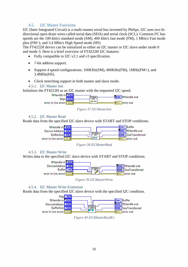
4.5. I2C Master Functions I2C (Inter Integrated Circuit) is a multi-master serial bus invented by Philips. I2C uses two bi-
directional open-drain wires called serial data (SDA) and serial clock (SCL). Common I²C bus
speeds are the 100 kbit/s standard mode (SM), 400 kbit/s fast mode (FM), 1 Mbit/s Fast mode
plus (FM+), and 3.4 Mbit/s High Speed mode (HS)
The FT4222H device can be initialized as either an I2C master or I2C slave under mode 0
and mode 3. Here is a brief overview of FT4222H I2C features:
• Fully compatible to I2C v2.1 and v3 specification.
• 7-bit address support.
• Support 4 speed configurations: 100KHz(SM), 400KHz(FM), 1MHz(FM+), and
3.4MHz(HS).
• Clock stretching support in both master and slave mode.
4.5.1. I2C Master Init
Initializes the FT4222H as an I2C master with the requested I2C speed.
Figure 37 I2CMasterInit
4.5.2. I2C Master Read
Reads data from the specified I2C slave device with START and STOP conditions.
Figure 38 I2CMasterRead
4.5.3. I2C Master Write
Writes data to the specified I2C slave device with START and STOP conditions.
Figure 39 I2CMasterWrite
4.5.4. I2C Master Write Extension
Reads data from the specified I2C slave device with the specified I2C condition.
Figure 40 I2CMasterReadEx
16
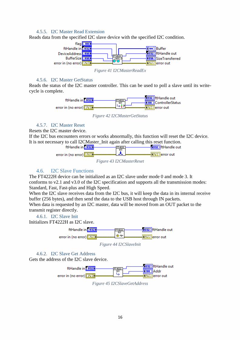
4.5.5. I2C Master Read Extension
Reads data from the specified I2C slave device with the specified I2C condition.
Figure 41 I2CMasterReadEx
4.5.6. I2C Master GetStatus
Reads the status of the I2C master controller. This can be used to poll a slave until its write-
cycle is complete.
Figure 42 I2CMasterGetStatus
4.5.7. I2C Master Reset
Resets the I2C master device.
If the I2C bus encounters errors or works abnormally, this function will reset the I2C device.
It is not necessary to call I2CMaster_Init again after calling this reset function.
Figure 43 I2CMasterReset
4.6. I2C Slave Functions The FT4222H device can be initialized as an I2C slave under mode 0 and mode 3. It
conforms to v2.1 and v3.0 of the I2C specification and supports all the transmission modes:
Standard, Fast, Fast-plus and High Speed.
When the I2C slave receives data from the I2C bus, it will keep the data in its internal receive
buffer (256 bytes), and then send the data to the USB host through IN packets.
When data is requested by an I2C master, data will be moved from an OUT packet to the
transmit register directly.
4.6.1. I2C Slave Init
Initializes FT4222H as I2C slave.
Figure 44 I2CSlaveInit
4.6.2. I2C Slave Get Address
Gets the address of the I2C slave device.
Figure 45 I2CSlaveGetAddress

17
4.6.3. I2C Slave Set Address
Sets the address of the I2C slave device.
Figure 46 I2CSlaveSetAddress
4.6.4. I2C Slave Get Rx Status
Gets number of bytes in the receive queue.
Figure 47 I2CSlaveGetRxStatus
4.6.5. I2C Slave Read
Reads data from the buffer of the I2C slave device.
Figure 48 I2CSlaveRead
4.6.6. I2C Slave Write
Writes data to the buffer of I2C slave device.
Figure 49 I2CSlaveWrite
4.6.7. I2C Slave Reset
Resets the I2C slave device.
Figure 50 I2CSlaveReset

18
4.7. GPIO Functions The FT4222H contains 4 GPIO. When the USB GPIO interface is supported, chip mode 0 and
mode 1, LibFT4222 helps application developers to control GPIO directly. However, each
GPIO pin is multiplexed with interrupt/suspend out/SPI slave select/I2C functions as listed
below:
• gpio0 / ss1o / scl
• gpio1 / ss2o / sda
• gpio2 / ss3o / suspend out
• gpio3 / wakeup/intr
The number of GPIO pins available depends on the mode of the chip. For example, if the
FT4222H is initialized as an I2C device, as shown above, the pins of gpio0 and gpio1 will be
switched to scl and sda, and cannot be used as GPIO. If suspend out and remote wakeup are
enabled gpio2 and gpio3 cannot be used as GPIO.
The FT4222H supports GPIO on the second USB interface in mode 0 or on the fourth interface
in mode 2 (Please refer table 2.1 for chip mode and interface).
4.7.1. GPIO Init
Initializes the GPIO interface of the FT4222H.
Please note the GPIO interface is available on the 2nd USB interface in mode 0 or on the 4th
USB interface in mode 1.
Figure 51 GPIOInit
4.7.2. GPIO Read
Reads the value from the specified GPIO pin.
Figure 52 GPIORead
4.7.3. GPIO Write
Writes value to the specified GPIO pin.
Figure 53 GPIOWrite

19
4.7.4. GPIO Set Input Trigger
Set software trigger conditions on the specified GPIO pin.
This function allows developers to monitor value changes of the GPIO pins. Values that satisfy
the trigger condition will be stored in a queue. For example, if GPIO_TRIGGER_RISING is
set on GPIO0, and GPIO0 then changes value from 0 to 1, the event GPIO_TRIGGER_RISING
will be recorded into the queue. Developers can query the queue status by
FT4222_GPIO_GetTriggerStatus, and FT4222_GPIO_ReadTriggerQueue.
Figure 54 GPIOSetInputTriggers
4.7.5. GPIO Get Trigger Status
Gets the size of trigger event queue.
Figure 55 GPIOGetTriggerStatus
4.7.6. GPIO Read Trigger Queue
Gets events are recorded in the trigger event queue. Trigger conditions are set by a call to
FT4222_GPIO_SetInputTrigger. After calling this function, all events will be removed from
the event queue.
Figure 56 GPIOReadTriggerQueue
5. Examples
The package installs an example VIs into the Example Finder.
In order to open VIs using the NI Example Finder, please select "Browse according to
Directory Structure" and navigate to the “Ovak Technologies” folder.
5.1. SPI – Single Slave Example
Figure 57 SPI - Single Slave Example

20
With a single SPI slave device, it is connected with a 1:1 relationship between signals. Some
SPI devices do not have both data in and data out signals. For example an analogue to digital
converter may not have a MOSI data input, and a digital to analogue converter may not have
a MISO data output. The signals on the FTx232D/H chips have internal pull-ups, so they
may be left unconnected if they are not used. The CS signal is used to enable the slave device’s
interface. With only one device, it may be acceptable to tie the chip select to always-active
state.
Figure 58 SPI Single Slave Example
“SPI Single Slave” example VI implements a Single Slave SPI bus connection. It
performs a full-duplex transfer of data with the slave device. Data (an array of bytes) is
both sent to the slave and received from the slave at once.
5.2. SPI – Multiple Slaves Example Circuit
Figure 59 SPI - Multiple Slaves Example Circuit

21
Multiple SPI slaves share data in, data out and clock signals; however, each requires a
unique CS signal. Any of the available GPIO signals, in addition to the MPSSE CS signal
can be used as additional chip selects. In this case only one slave device can be active. The
application program must keep track of which SPI slave device is enabled. As with the
single-slave connection, unused DIO signals can be left unconnected.
Figure 60 SPI Multiple Slaves Example
“SPI Multiple Slaves” example VI implements a Multiple Slave SPI bus connection. It
performs a full-duplex transfer of data with the slave devices. Data is both sent to the slave
and received from the slave at once.
For applications those have uncommon register sizes (not a multiple of 8 bits), “Bit Data”
mode can be selected from “Write-Read.vi” Polymorphic VI’s drop-down menu.
5.3. FT4222 SPI Master Example Initializes device’s clock, mode, and strengths. Builds buffers, sends to SPI Slave and reads
received buffers and uninitializes.
Figure 61 FT4222 SPI Master Example

22
5.4. FT4222 SPI Slave Example Initializes device. When buffer is received it reads and displays. Then it uninitializes and closes
all references.
Figure 62 FT4222 SPI slave Example
5.5. I2C – Single Slave Example Circuit
Figure 63 I2C - Single Slave Example Circuit
I2C is a bidirectional, half-duplex communication scheme. Although the full specification
allows for multiple-masters, the MPSSE can only interface with I2C slave devices. The I2C
interface can be implemented with the connection shown in Figure above In addition, the
application software will need to include steps to change the direction of the MPSSE DO signal
in order to eliminate any bus contention.
Figure 64 I2C Single Slave Example
“I2C Single Slave” example VI implements a combined write and read operations in a single
slave I2C bus configuration.
23
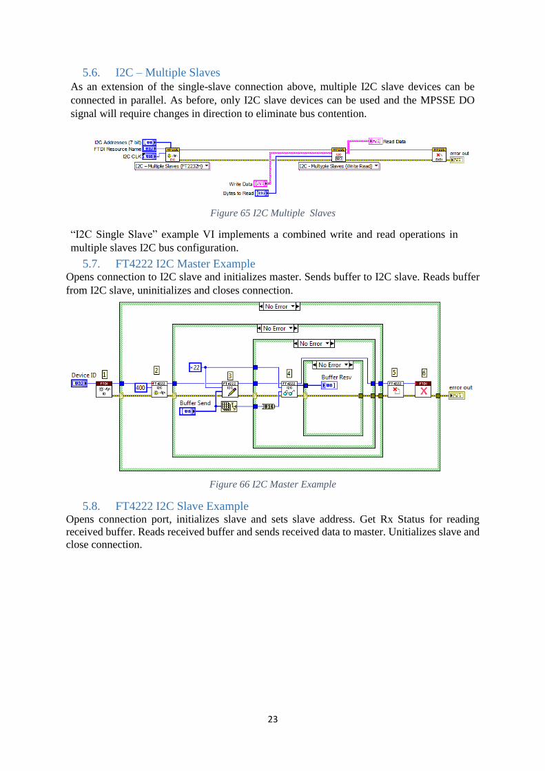
5.6. I2C – Multiple Slaves
As an extension of the single-slave connection above, multiple I2C slave devices can be
connected in parallel. As before, only I2C slave devices can be used and the MPSSE DO
signal will require changes in direction to eliminate bus contention.
Figure 65 I2C Multiple Slaves
“I2C Single Slave” example VI implements a combined write and read operations in
multiple slaves I2C bus configuration.
5.7. FT4222 I2C Master Example Opens connection to I2C slave and initializes master. Sends buffer to I2C slave. Reads buffer
from I2C slave, uninitializes and closes connection.
Figure 66 I2C Master Example
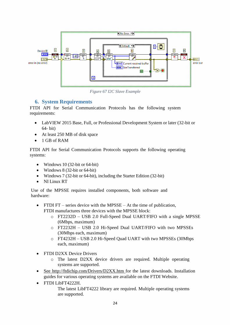
5.8. FT4222 I2C Slave Example Opens connection port, initializes slave and sets slave address. Get Rx Status for reading
received buffer. Reads received buffer and sends received data to master. Unitializes slave and
close connection.
24
Figure 67 I2C Slave Example
6. System Requirements FTDI API for Serial Communication Protocols has the following system
requirements:
• LabVIEW 2015 Base, Full, or Professional Development System or later (32-bit or
64- bit)
• At least 250 MB of disk space
• 1 GB of RAM
FTDI API for Serial Communication Protocols supports the following operating
systems:
• Windows 10 (32-bit or 64-bit)
• Windows 8 (32-bit or 64-bit)
• Windows 7 (32-bit or 64-bit), including the Starter Edition (32-bit)
• NI Linux RT
Use of the MPSSE requires installed components, both software and
hardware:
• FTDI FT – series device with the MPSSE – At the time of publication,
FTDI manufactures three devices with the MPSSE block:
o FT2232D – USB 2.0 Full-Speed Dual UART/FIFO with a single MPSSE
(6Mbps, maximum)
o FT2232H – USB 2.0 Hi-Speed Dual UART/FIFO with two MPSSEs
(30Mbps each, maximum)
o FT4232H – USB 2.0 Hi-Speed Quad UART with two MPSSEs (30Mbps
each, maximum)
• FTDI D2XX Device Drivers
o The latest D2XX device drivers are required. Multiple operating
systems are supported.
• See http://ftdichip.com/Drivers/D2XX.htm for the latest downloads. Installation
guides for various operating systems are available on the FTDI Website.
• FTDI LibFT4222H.
The latest LibFT4222 library are required. Multiple operating systems
are supported.

25
• Documentation
o Datasheet for the FTDI FT-series device with the MPSSE
o D2XX Programmers Guide
o AN_108 Command Processor for MPSSE and MCU Host Bus Emulation
Modes
7. Suggested connections Each type of interface has some unique circuitry requirements. With such a diverse
selection of peripheral devices, not every interface can be covered here. The
implementations below ill serve as a starting point for each popular interfaces.
For the FTDI USB Hi-Speed devices (FT2232H and FT4232H), the I/O interface operates at
3.3V. The pins are 5V-tolerant, so it is possible to directly connect 5V devices to the
interface. For the FTDI USB Full-Speed device (FT2232D), the I/O interface operates at
the voltage applied to VCCIO.
Note: Care should be taken to review all datasheets for the devices to
ensure I/O threshold and maximum voltages are met.
8. Support Information For technical support, please, contact Ovak Technologies at:
Phone: + 374 10 21-97-68
Email: [email protected]
Web: www.ovaktechnologies.com
Related Documents


