University of Benghazi بنغازي جامعةFaculty of Education Al marj جية التربية المر كلGlobal Libyan Journal لعالميةليبية اة المجل اللسابعد ا العد– مايو1026 1 Frequency modulation and demodulation using digital phase locked loop. ــــــــــــــــــــــــــــــــــــــــــــــــــــــــــــــ ــــــــــــــــــــــــــــــــــــــــــــــــــــــDear * Khadija Rajab Al Shari ** Ahmed El barsha. (Benghazi University, Faculty of Engineering, Electrical and Electronic Engineering Department – Libya)

Welcome message from author
This document is posted to help you gain knowledge. Please leave a comment to let me know what you think about it! Share it to your friends and learn new things together.
Transcript
University of Benghazi جامعة بنغازي
Faculty of Education Al marj كلية التربية المر ج Global Libyan Journal المجلة الليبية العالمية
1026 مايو – العدد السابع
1
Frequency modulation and demodulation using digital
phase locked loop.
ــــــــــــــــــــــــــــــــــــــــــــــــــــــــــــــــــــــــــــــــــــــــــــــــــــــــــــــــــــ Dear * Khadija Rajab Al Shari ** Ahmed El barsha.
(Benghazi University, Faculty of Engineering, Electrical and Electronic Engineering
Department – Libya)
University of Benghazi جامعة بنغازي
Faculty of Education Al marj كلية التربية المر ج Global Libyan Journal المجلة الليبية العالمية
1026 مايو – العدد السابع
2
Frequency modulation and demodulation using digital phase locked loop.
By:
Khadija Rajab Al Shari, Ahmed El barsha.
Benghazi University, Faculty of Engineering, Electrical and Electronic Engineering
Department.
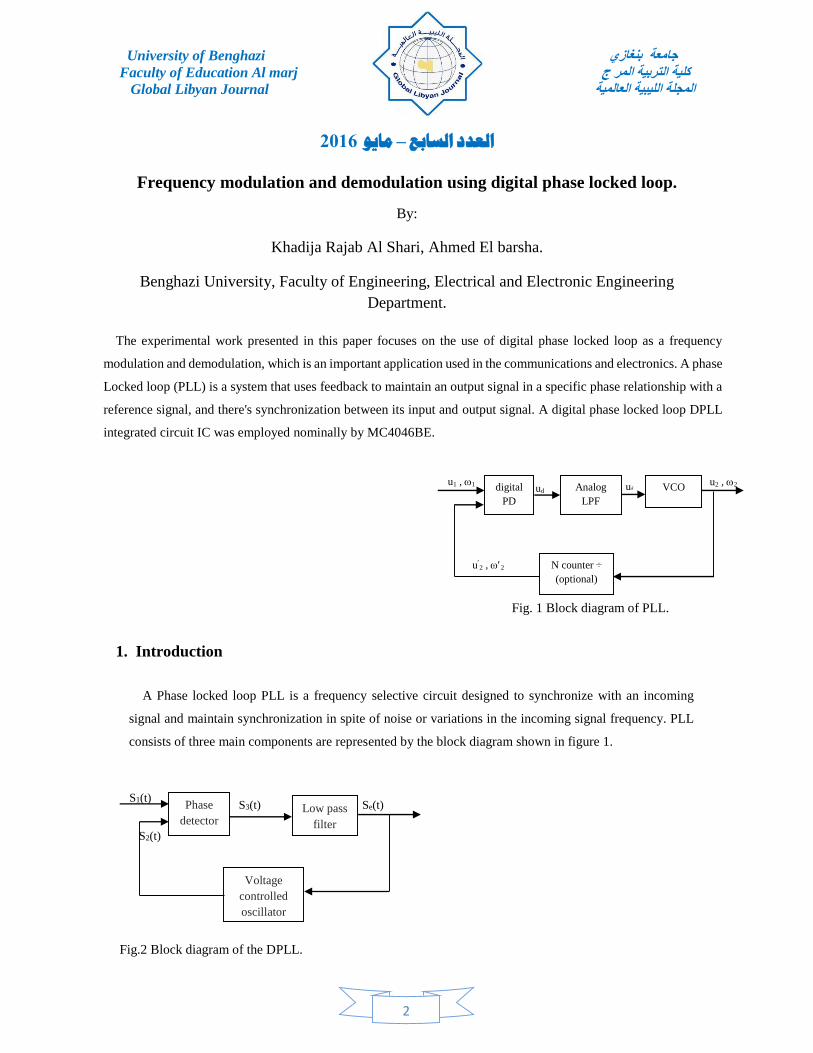
The experimental work presented in this paper focuses on the use of digital phase locked loop as a frequency
modulation and demodulation, which is an important application used in the communications and electronics. A phase
Locked loop (PLL) is a system that uses feedback to maintain an output signal in a specific phase relationship with a
reference signal, and there's synchronization between its input and output signal. A digital phase locked loop DPLL
integrated circuit IC was employed nominally by MC4046BE.
Fig. 1 Block diagram of PLL.
1. Introduction
A Phase locked loop PLL is a frequency selective circuit designed to synchronize with an incoming
signal and maintain synchronization in spite of noise or variations in the incoming signal frequency. PLL
consists of three main components are represented by the block diagram shown in figure 1.
Fig.2 Block diagram of the DPLL.
Se(t) S3(t)
S2(t)
S1(t) Phase
detector Low pass
filter
Voltage
controlled
oscillator
uf ud u2 , 2
u2 , 2
u1 , 1 digital
PD
Analog
LPF
VCO
N counter ÷
(optional)
University of Benghazi جامعة بنغازي
Faculty of Education Al marj كلية التربية المر ج Global Libyan Journal المجلة الليبية العالمية
1026 مايو – العدد السابع
3
1.1 Digital phase locked loop
The digital phase locked loop (DPLL) has the same construction of the linear phase locked loop except that
the DPLL consists of digital and analog components (Hybrid system). The only digital component is the phase
comparator and the other components are linear, and contains also an additional block component is a digital
counter as shown in figure 2.
In the digital phase locked loop, the phase comparator is one of three types: EXOR gate, JK flip-flop and
phase frequency detector (PFD). [1][2].
2. PLL characteristics
2.1 Free running frequency (fo, o)
Also called the center frequency, this is the frequency which the loop (VCO) operates when not locked to
an input signal.
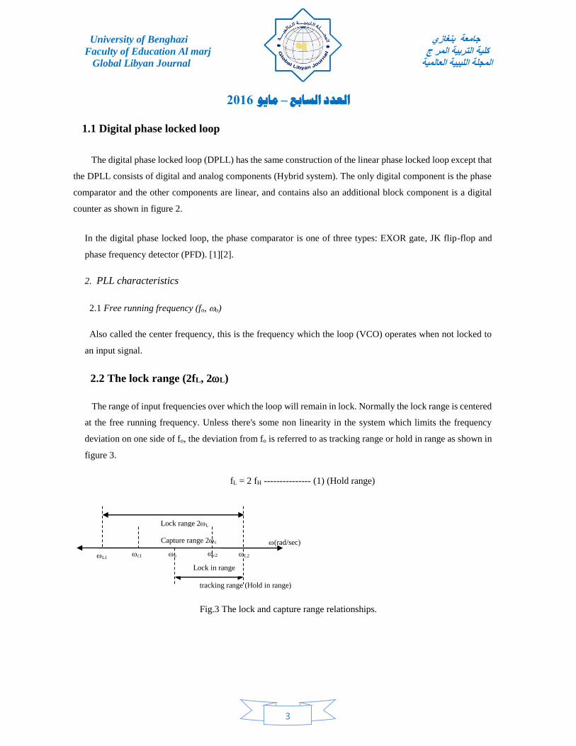
2.2 The lock range (2fL, 2L)
The range of input frequencies over which the loop will remain in lock. Normally the lock range is centered
at the free running frequency. Unless there's some non linearity in the system which limits the frequency
deviation on one side of fo, the deviation from fo is referred to as tracking range or hold in range as shown in
figure 3.
fL = 2 fH --------------- (1) (Hold range)
Fig.3 The lock and capture range relationships.
o c2 L2 L1 c1
tracking range (Hold in range)
Lock range 2L
Capture range 2c (rad/sec)
Lock in range
University of Benghazi جامعة بنغازي
Faculty of Education Al marj كلية التربية المر ج Global Libyan Journal المجلة الليبية العالمية
1026 مايو – العدد السابع
4
4.3 Capture range (2fc, 2c)
Sometimes the loop may not be able to acquire lock at the tracking range extremes because of the selectivity
afforded by the low pass filter. The capture range is also centered at fo with equal deviation the capture range
is also called the pull-in range . The capture range can never exceed the lock range. [2].
5. Experimental work
The MC4046BE is one of the most versatile CMOS chips, among the many application of the 4046 are
those in frequency modulation, voltage to frequency conversion, frequency synthesis, tone decoding, FSK
demodulation and frequency multiplication. The 4046 is studied along with its characteristics and
applications. Some of these applications have been carried out experimentally. [4].
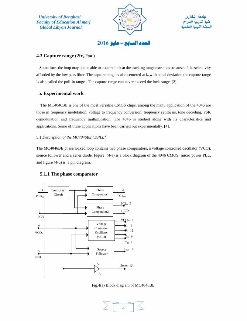
5.1 Description of the MC4046BE "DPLL"
The MC4046BE phase locked loop contains two phase comparators, a voltage controlled oscillator (VCO),
source follower and a zener diode. Figure (4-a) is a block diagram of the 4046 CMOS micro power PLL,
and figure (4-b) is a pin diagram.
5.1.1 The phase comparator
Fig.4(a) Block diagram of MC4046BE.
INH
VCOin
PCBin
3
PCAin
14
Zener 15
SFout 10
C1B 7
C1A 6
R2 12
R1 11
VCOout 4
1 LD
PC2ou13
PC1out
2
5
9
Self Bias
Circuit
Phase
Comparator1
Phase
Comparator2
Voltage
Controlled
Oscillator
(VCO)
Source
Follower
University of Benghazi جامعة بنغازي
Faculty of Education Al marj كلية التربية المر ج Global Libyan Journal المجلة الليبية العالمية
1026 مايو – العدد السابع
5
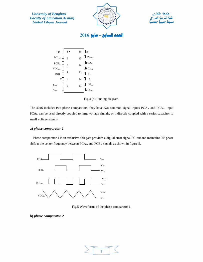
Fig.4 (b) Pinning diagram.
The 4046 includes two phase comparators, they have two common signal inputs PCAin and PCBin. Input
PCAin can be used directly coupled to large voltage signals, or indirectly coupled with a series capacitor to
small voltage signals.
a) phase comparator 1
Phase comparator 1 is an exclusive-OR gate provides a digital error signal PC1out and maintains 90o phase
shift at the center frequency between PCAin and PCBin signals as shown in figure 5.
Fig.5 Waveforms of the phase comparator 1.
b) phase comparator 2
Zener
VCOin
SFout
R1
R2
PC2out
PCAin
VDD
VSS
C1B
C1A
INH
VCOout
PCBin
PC1out
LD 1 16
2 15
3 14
4 13
5 12
6 11
7 10
PC1out
PCBin
PCAin
VCOin
VOL
VOL
VOH
VOL
VSS
VOH
VOH
University of Benghazi جامعة بنغازي
Faculty of Education Al marj كلية التربية المر ج Global Libyan Journal المجلة الليبية العالمية
1026 مايو – العدد السابع
6
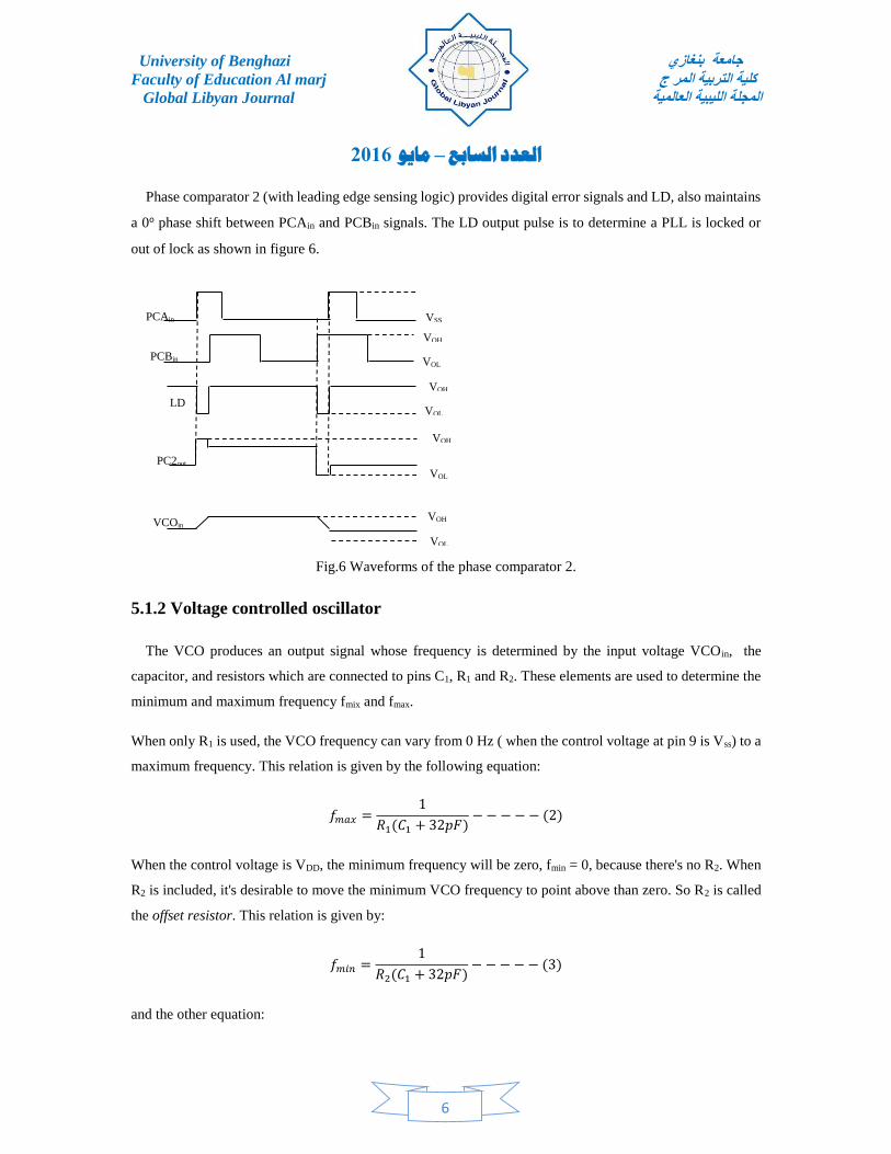
Phase comparator 2 (with leading edge sensing logic) provides digital error signals and LD, also maintains
a 0o phase shift between PCAin and PCBin signals. The LD output pulse is to determine a PLL is locked or
out of lock as shown in figure 6.
Fig.6 Waveforms of the phase comparator 2.
5.1.2 Voltage controlled oscillator
The VCO produces an output signal whose frequency is determined by the input voltage VCOin, the
capacitor, and resistors which are connected to pins C1, R1 and R2. These elements are used to determine the
minimum and maximum frequency fmix and fmax.
When only R1 is used, the VCO frequency can vary from 0 Hz ( when the control voltage at pin 9 is Vss) to a
maximum frequency. This relation is given by the following equation:
𝑓𝑚𝑎𝑥 =1
𝑅1(𝐶1 + 32𝑝𝐹)− − − − − (2)
When the control voltage is VDD, the minimum frequency will be zero, fmin = 0, because there's no R2. When
R2 is included, it's desirable to move the minimum VCO frequency to point above than zero. So R2 is called
the offset resistor. This relation is given by:
𝑓𝑚𝑖𝑛 =1
𝑅2(𝐶1 + 32𝑝𝐹)− − − − − (3)
and the other equation:
VOH
VOL
VOL
VOH
VOL
VOH
VOL
VOH
VCOin
PC2out
LD
PCBin
PCAin
VSS
University of Benghazi جامعة بنغازي
Faculty of Education Al marj كلية التربية المر ج Global Libyan Journal المجلة الليبية العالمية
1026 مايو – العدد السابع
7
𝑓𝑚𝑎𝑥 =1
𝑅1(𝐶1 + 32𝑝𝐹)+ 𝑓𝑚𝑖𝑛 − − − −− (4)
5.1.3 The source follower
The source follower output SFout is used with external resistor, where the input voltage of VCO is needed
but no loaded can be tolerated. The inhibit input INH (when it's high), disables the VCO and the source
follower to minimize standby power consumption. The zener diode can be used to assist in power supply
regulation. The self bias circuit adjusts small voltage signals in the linear region of the amplifier.
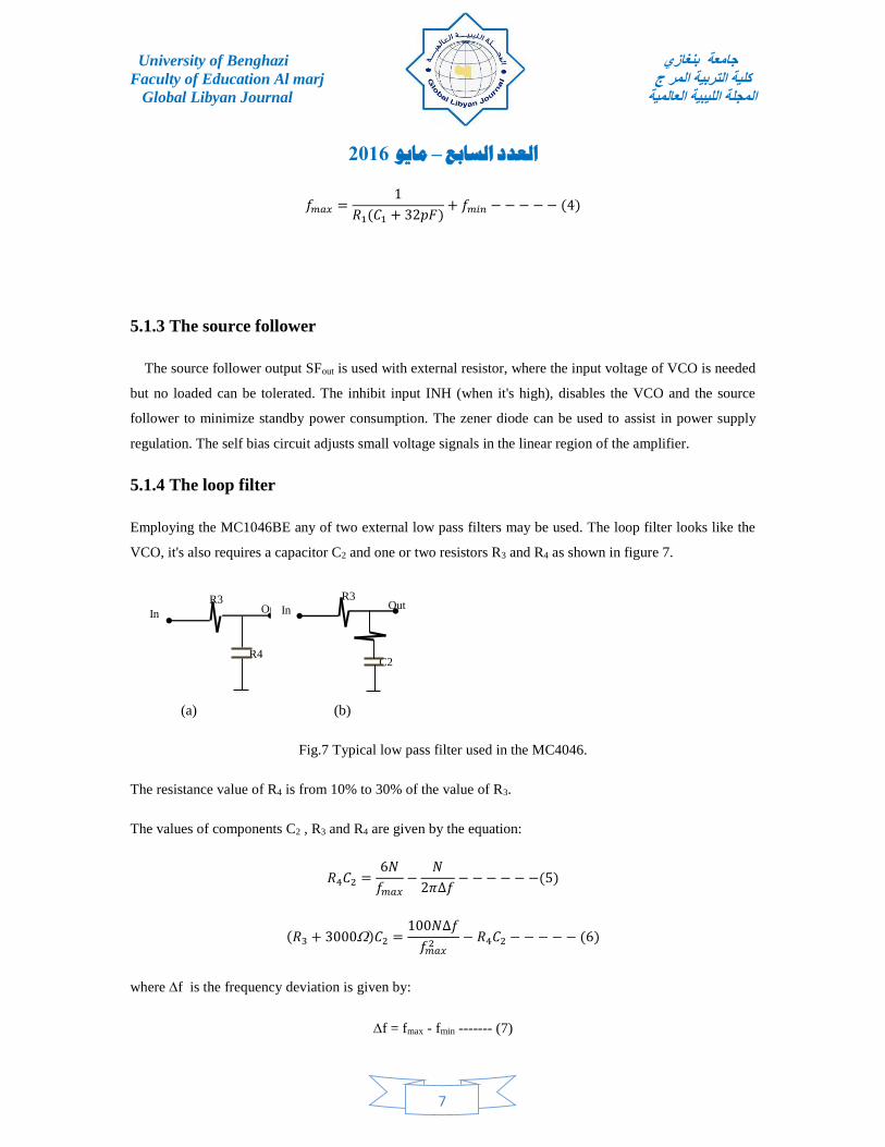
5.1.4 The loop filter
Employing the MC1046BE any of two external low pass filters may be used. The loop filter looks like the
VCO, it's also requires a capacitor C2 and one or two resistors R3 and R4 as shown in figure 7.
(a) (b)
Fig.7 Typical low pass filter used in the MC4046.
The resistance value of R4 is from 10% to 30% of the value of R3.
The values of components C2 , R3 and R4 are given by the equation:
𝑅4𝐶2 =6𝑁
𝑓𝑚𝑎𝑥
−𝑁
2𝜋∆𝑓− −− − − −(5)
(𝑅3 + 3000)𝐶2 =100𝑁∆𝑓
𝑓𝑚𝑎𝑥2
− 𝑅4𝐶2 − − −− − (6)
where f is the frequency deviation is given by:
f = fmax - fmin ------- (7)
R4
C2
In Out R3
C2
In Out R3
University of Benghazi جامعة بنغازي
Faculty of Education Al marj كلية التربية المر ج Global Libyan Journal المجلة الليبية العالمية
1026 مايو – العدد السابع
8
N is the total deviation ratio in feedback loop. [2] [3]
5.2 Experimental work with MC4046BE "DPLL"
Some of the important applications are realized practically using the MC4046BE are frequency modulation
and demodulation.
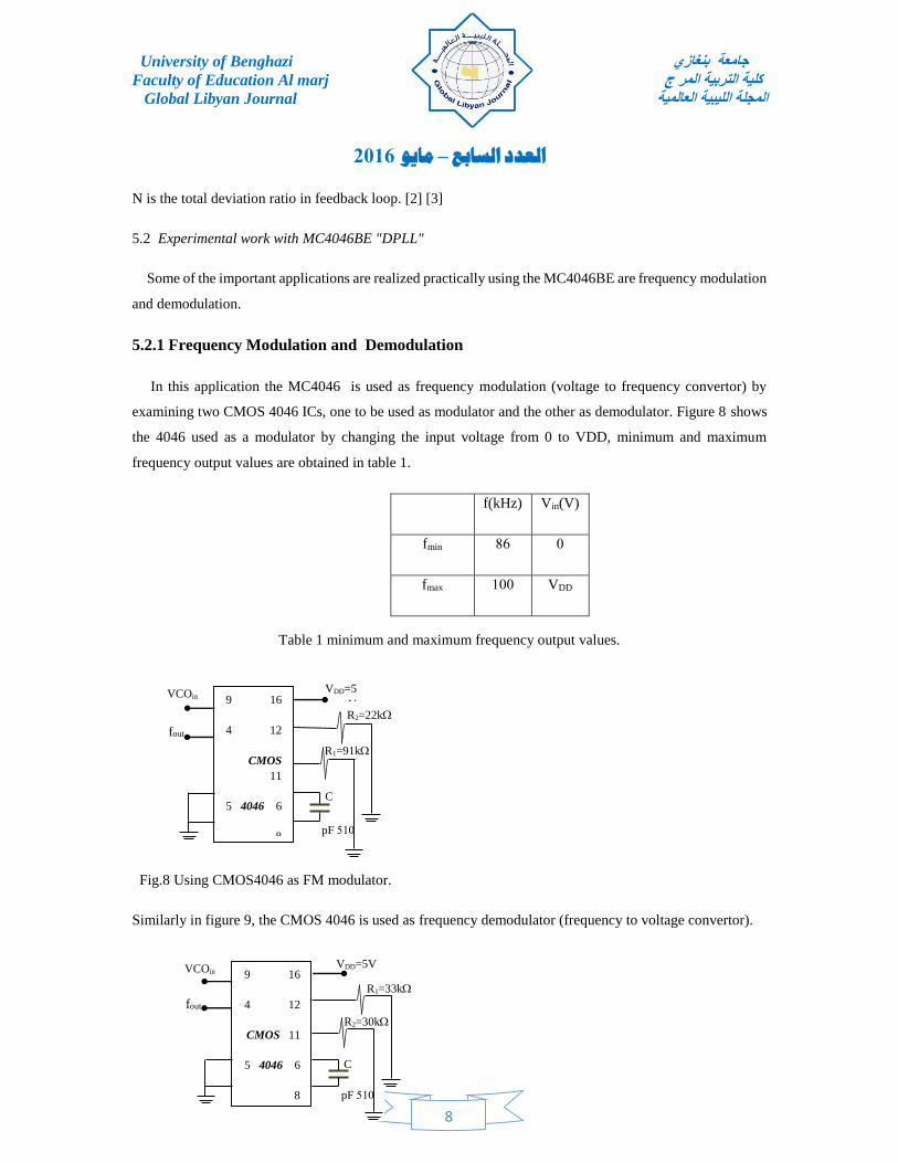
5.2.1 Frequency Modulation and Demodulation
In this application the MC4046 is used as frequency modulation (voltage to frequency convertor) by
examining two CMOS 4046 ICs, one to be used as modulator and the other as demodulator. Figure 8 shows
the 4046 used as a modulator by changing the input voltage from 0 to VDD, minimum and maximum
frequency output values are obtained in table 1.
Table 1 minimum and maximum frequency output values.
Fig.8 Using CMOS4046 as FM modulator.
Similarly in figure 9, the CMOS 4046 is used as frequency demodulator (frequency to voltage convertor).
Vin(V) f(kHz)
0 66 fmin
VDD 100 fmax
C
VDD=5
V
R1=91k
pF 510
fout
VCOin 9 16
4 12
CMOS
11
5 4046 6
8
R2=22k
C
VDD=5V
R2=30k
pF 510
fout
VCOin 9 16
4 12
CMOS 11
5 4046 6
8
R1=33k
University of Benghazi جامعة بنغازي
Faculty of Education Al marj كلية التربية المر ج Global Libyan Journal المجلة الليبية العالمية
1026 مايو – العدد السابع
9
Fig.9 Using CMOS4046 as FM demodulator.
Table 2 minimum and maximum frequency output values.
Fig.10 Frequency modulator and demodulator.
Vin(V) f(kHz)
0 77 fmin
VDD 111 fmax
ch2
2Vpp
51
1kHz
VCO
9 4046 4
12 11 6 7
Modulator stage
Demodulator stage
FM
0.02F
620
510pF
30k
33k
VCO
9 4046 4
12 11 6 7
10
10k
SF
14 PC
CMOS 3
4046 2
ch1
demodulator
ch2
ch1
5ms/div
ch1
ch2
5ms/div
ch2
ch1
5ms/div
University of Benghazi جامعة بنغازي
Faculty of Education Al marj كلية التربية المر ج Global Libyan Journal المجلة الليبية العالمية
1026 مايو – العدد السابع
10
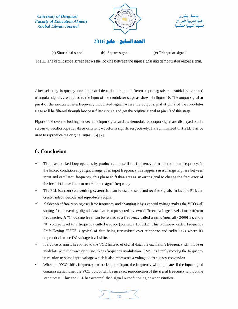
(a) Sinusoidal signal. (b) Square signal. (c) Triangular signal.
Fig.11 The oscilloscope screen shows the locking between the input signal and demodulated output signal.
After selecting frequency modulator and demodulator , the different input signals: sinusoidal, square and
triangular signals are applied to the input of the modulator stage as shown in figure 10. The output signal at
pin 4 of the modulator is a frequency modulated signal, where the output signal at pin 2 of the modulator
stage will be filtered through low pass filter circuit, and get the original signal at pin 10 of this stage.
Figure 11 shows the locking between the input signal and the demodulated output signal are displayed on the
screen of oscilloscope for three different waveform signals respectively. It's summarized that PLL can be
used to reproduce the original signal. [5] [7].
6. Conclusion
The phase locked loop operates by producing an oscillator frequency to match the input frequency. In
the locked condition any slight change of an input frequency, first appears as a change in phase between
input and oscillator frequency, this phase shift then acts as an error signal to change the frequency of
the local PLL oscillator to match input signal frequency.
The PLL is a complete working system that can be used to send and receive signals. In fact the PLL can
create, select, decode and reproduce a signal.
Selection of free running oscillator frequency and changing it by a control voltage makes the VCO well
suiting for converting digital data that is represented by two different voltage levels into different
frequencies. A "1" voltage level can be related to a frequency called a mark (normally 2000Hz), and a
"0" voltage level to a frequency called a space (normally 1500Hz). This technique called Frequency
Shift Keying "FSK" is typical of data being transmitted over telephone and radio links where it's
impractical to use DC voltage level shifts.
If a voice or music is applied to the VCO instead of digital data, the oscillator's frequency will move or
modulate with the voice or music, this is frequency modulation "FM". It's simply moving the frequency
in relation to some input voltage which it also represents a voltage to frequency conversion.
When the VCO shifts frequency and locks to the input, the frequency will duplicate, if the input signal
contains static noise, the VCO output will be an exact reproduction of the signal frequency without the
static noise. Thus the PLL has accomplished signal reconditioning or reconstitution.
University of Benghazi جامعة بنغازي
Faculty of Education Al marj كلية التربية المر ج Global Libyan Journal المجلة الليبية العالمية
1026 مايو – العدد السابع
11
The VCO is exactly synchronized with an incoming signal, it can be amplified, filtered and used to
"Clock" the signal or give synchronizing information necessary to lock at the input signal. [1] [4].
References
[1] R. E. Best, "Phase locked loop: Design, Simulation and applications", 3rd Ed., Mc Graw- Hill, New
York, 1997.
[2] P. Horowitz and W. Hill, "The art of electronics", 2nd Ed., Cambridge 1998.
[3] S. Franco, "Design with operational amplifiers an analog integrated circuits", 2nd Ed., Mc Graw- Hill,
New York, 1997.
[4] Comer D. J., "Electronic design with integrated circuits", Addison Wesley publishing company, 1998.
[5] P. H. Young, Electronic communication techniques", 3rd Ed., Prentice Hill, 1990.
[6] "An overview of phase locked loop", Application note AN-177, Philips Semiconductors, Dec. 1998.
[7] "Phase locked loop design fundamentals", Application note AN-535, Motorola Inc., 1994.
Related Documents